1
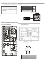
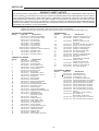
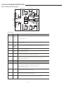
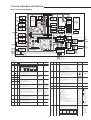
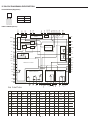
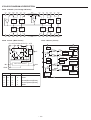
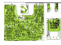
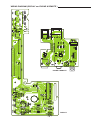
FILE NO.
Service Manual
Micro Component System
CONTENTS
DC-MCR50 (XE)
PRODUCT CODE No.
129 664 02
Laser beam safety precaution .......................................... 1
Block diagram .................................................................. 1, 7
Tuner Adjustment ............................................................. 2
Exploded View (Cabinet & Chassis) ................................ 3
Parts List .......................................................................... 4
Schematic Diagram (Main) .............................................. 12
Wiring Diagram (CD Main, CD Door Sw, LED1, LED2,
and Audio) ......................................... 14
Wiring Diagram (Display and Phone & Remote) ............ 16
Wiring Connection ........................................................... Rear
REFERENCE No. SM5810404
LASER BEAM SAFETY PRECAUTION
• Pick-up that emits a laser beam is used in this CD player section.
CAUTION – INVISIBLE LASER RADIATION WHEN OPEN AND
INTERLOCKS DEFEATED. AVOID EXPOSURE TO BEAM.
ADVARSEL – USYNLIG LASER STRÅLING VED ÅBNING, NÅR
SIKKERHEDSAFBRYDERE ER UDE AF FUNKTION, UNDGÅ UDS ÆTTELSE
FOR STRÅLING.
VARNING – OSYNLIG LASER STRÅLNING NÄR DENNA DEL ÄR ÖPPNAD
OCH SPÄRR ÄR URKOPPLAD. STRÅLEN ÄR FARLIG.
VORSICHT – UNSICHTBARE LASERSTRAHLUNG TRITT AUS, WENN
DECKEL GEÖFFNET UND WENN SICHERHEITSVERRIEGELUNG
ÜBERBRÜCKT IST. NICHT, DEM STRAHL AUSSETZEN.
VARO – AVATTAESSA JA SUOJALUKITUS OHITETTAESSA OLET ALTTIINA
NÄKYMÄTTÖMÄLLE LASERSÄTEILYLLE. ÄLÄ KATSO SÄTEESEEN.
CAUTION :
USE OF CONTROLS OR ADJUSTMENTS
OR PERFORMANCE OF PROCEDURES
OTHER THAN THOSE SPECIFIED HEREIN
MAY RESULT IN HAZARDOUS RADIATION
EXPOSURE
LASER OUTPUT .......... 0.6 mW Max. (CW)
WAVELENGTH ............. 790 nm
IC BLOCK DIAGRAM & DESCRIPTION
11
10
AM
IF
FM
IF
12
AGC
AM
DET
FM
S-METER
9
GND1
7
6
IF
BUFFER
8
ST
SD
TRIG
VCO
ST SW
MUTE
DECODER
FF
FF
FF
FM
DET
PILOT
DET
PHASE
COMP
IC102 LC72131 (PLL)
19
18
17
16
15
14
13
IC101 LA1823 (FM/AM MIX.)
VCC1
4
REG
2
3
1
1
AM
MIX
AM
RF
AM
OSC
OSC
BUFFER
5
FM
MIX
FM
OSC
VCC2
GND2
FM
RF
24
23
22
21
20
IC401 KIA7808 (Regulator)
- 1 -
2
3
Pin No.
Function
1
INPUT
2
COMMON
3
OUTPUT
TUNER ADJUSTMENTS
Use a plastic screw driver for adjustments.
Adjust the intermediate frequency of AM and FM to the frequency of ceramic filter.
Supply voltage
:
DC 12.0V
Phones impedance
:
32 ohms
Function switch
:
RADIO
a. Parts Location
b. AM Adjustment
Step Adjusting
circuit
BAND SELECT SWITCH: AM.
Tuning
Input Connection
Frequency Measurement
Input
Output Connection
Measurement
Output
Adjustment
Parts
VTVM Oscilloscope
OR VT. VOLT.
IC101PIN19(H)
1
IF
999 kHz
(450 KHz)
2
Tuning
3
Coverage
4
5
Genertor
1611 kHz
1404 kHz
b. FM Adjustment
Ste p Adjusting
circuit
1
2
3
4
5
Tuning
Frequency
Generator
Loop ANT
Input Connection
Measurement
Input
FM Sweep
IC101(5)H
Genertor
IC101(6) E
87.5 MHz
108 MHz
90.0 MHz
Tracking
AM Signal
VTVM
Oscilloscope
106.0 MHz
FM Signal
Generator
C110 (H)
IC101(6)E
IC101PIN6(E)
Digital
C131(H),
Voltmeter
C131(E)
VTVM
Oscilloscope
BAND SELECT SWITCH: FM.
IF
98.0 MHz
(10.70 MHz)
Tuning
Coverage
Loop ANT
522 KHz
603 kHz
Tracking
AM Sweep
C146TU(L)
IC101 pin6(E)
T102
T101
1.50V+/- 0.05 V
Confirm 7.8V+/-0.8 V
L106
TC101
Maximum
FM Dummy Antenna : 75 ohm unbalance
Output Connection
Measurement
Output
VTVM
Oscilloscope
IC101PIN6(E)
C105(H)
Voltmeter
C105(E)
- 2 -
VTVM Oscilloscope
Parts
IC101PIN19(H)
Digital
VTVM
Oscilloscope
Adjustment
C146TU(L)
IC101 pin6(E)
(Non-adjustment)
L103
2.0V+/- 0.2V
Confirm6,5V+/- 0.8V
L102
TC102
Maximum
49
50
52
51
53
54
S21
55
62
S22
56
S23
59
57
60
58
34
- 3 S14
46
45
S24
61
6
43
47
10
5
19
42
21
S18
S10
25
20
8
S2 S3 9
7
S17
S14
S16
40
26
44
39
S9
28
29
15
48
S11
S11
17
18
16
11
S1
3
1
S8
S4
29
13
4
36
51
S7
S5
31
14
53
35
50
52
32
27
62
12
49
33
S13
S14
49
2
54 55
S21
30
S6
56
S22
S23
63
59
60
57
58
S24
61
EXPLODED VIEW(CABINET & CHASSIS)
PARTS LIST
PRODUCT SAFETY NOTICE
EACH PRECAUTION IN THIS MANUAL SHOULD BE FOLLOWED DURING SERVICING. COMPONENTS IDENTIFIED WITH
THE IEC SYMBOL ! IN THE PARTS LIST AND THE SCHEMATIC DIAGRAM DESIGNATE COMPONENTS IN WHICH SAFETY
CAN OF SPECIAL SIGNIFICANCE. WHEN REPLACING A COMPONENT IDENTIFIED , USE ONLY THE REPLACEMENT
PARTS DESIGNATED, OR PARTS WITH THE SAME RATINGS OF RESISTANCE, WATTAGE OR VOLTAGE THAT ARE
DESIGNATED IN THE PARTS LIST IN THIS MANUAL. LEAKAGE-CURRENT OR RESISTANCE MEASUREMENTS MUST
BE MADE TO DETERMINE THAT EXPOSED PARTS ARE ACCEPTABLY INSULATED FROM THE SUPPLY CIRCUIT BEFORE
RETURNING THE PRODUCT TO THE CUSTOMER.
CAUTION :
Regular type resistors and capacitors are not listed. To know those values, refer to the schematic diagram.
Regular type resistors are less than 1/4W carbon type and 0 ohm chip resistors.
Regular type capacitors are less than 50V and less than 1000µF of Ceramic type and Electrolytic type.
PACKING & ACCESSORIES
FIXING PARTS
REF.NO.
REF.NO.
S10
S11
!
62
63
PART NO.
645 062 1918
645 027 2073
645 044 1943
645 062 2014
645 062 2007
645 062 2021
645 062 2083
645 023 3463
645 061 6280
645 061 6297
645 062 0652
645 062 0669
DESCRIPTION
INSTRUCTION MANUAL
POLY BAG,PWR CORD
POLY BAG,I/B
POLY BAG,UNIT
POLY BAG,SPK
POLY FOAM,KIT
CARTON CASE
POWER CORD
REMOTE CTL,RC29-100000-010
ANTENNA LOOP
SPK BOX L,LEFT
SPK BOX R,RIGHT
CABINET & CHASSIS
REF.NO.
1
2
3
4
6
7
8
9
11
12
15
16
17
18
19
20
21
26
27
28
29
30
PART NO.
645 062 1659
645 062 1437
645 062 1567
645 062 0591
645 062 1383
645 062 1284
645 062 1376
645 062 1420
645 062 1611
645 062 1628
645 062 1338
645 062 1321
645 062 1369
645 062 1505
645 062 1512
645 062 1352
645 062 1574
645 062 1345
645 062 1208
645 033 3446
645 027 1373
645 062 1635
31
33
34
35
36
40
43
45
46
47
48
49
645 062 1222
645 062 1307
645 062 1482
645 062 1499
645 062 1406
645 033 0391
645 055 7514
645 062 1598
645 062 1314
645 062 1536
645 062 1642
645 062 0584
DESCRIPTION
CD DOOR
CD DOOR BKT
CD DOOR LENS
ASSY CABINET TOP
PULLEY WORM GEAR
CD DOOR GEAR
MOTOR PULLEY
MOTOR BKT
TRANSPARNT LENS L
TRANSPARNT LENS R
KNOB BASS
KNOB TUNING
KNOB PRESS
KNOB CD DOOR,OPEN
KNOB FUNCTION
KNOB SW,MONO/STEREO
CD DISPLAY LENS
KNOB VOLUME
CD DECK MECHANISM
RUBBER SILICON,HARDNESS
WASHER METAL
CAB REAR COVER,
HEAT SINK COVER
HEAT SINK
CABINET MIDDLE
PANEL SIDE L,LEFT
PANEL SIDE R,RIGHT
AC SOCKET BKT
AC SKT COVER
REMOTE RECEIVER BKT
DECOR FRANT LENS
CABINET BOTTOM
REMOTE LENS
CABINET TOP
ASSY CABINET BOTTOM
PART NO.
DESCRIPTION
645 023 6594 SCREW ST 3X8,DISPLAY BD
645 023 6594 SCREW ST 3X8,ANT JACK,
OPTICAL JACK
645 023 6594 SCREW ST 3X8,AUX JACK,
RCA JACK
645 062 1116 SCR 3X15,CAB BTM TO CAB TOP
645 023 6617 SCREW ST 3X10,AC SOCKET
645 023 6594 SCREW ST 3X8,H/JACK BD
645 023 6594 SCREW ST 3X8,MAIN BD
645 062 1086 SCR 2X5,CD DOOR LENS
645 062 1109 SCR 2.6X4,MOTOR
645 023 6594 SCREW ST 3X8,MOTOR BKT
645 027 1168 SCR 3X8,CD DOOR SW
645 062 1116 SCR 3X15,
PWR TRANS TO CAB BTM
645 023 6594 SCREW ST 3X8,
H/S COVER TO CD TRAY
645 023 6587 SCREW ST 3X8,IC TO H/S
645 023 6594 SCREW ST 3X8,AUDIO BD
645 033 0247 SCR 2.6X8,CD DECK
S13
S14
S16
S17
S18
S1
S2
S3
S4
S5
S6
S7
S8
S9
ELECTRICAL-PARTS
REF.NO.
5
14
39
- 4 -
!
PART NO.
645 062 1215
645 062 0683
645 032 9760
645 062 0928
645 042 9569
645 062 1000
645 062 1017
645 062 1024
645 062 1031
645 062 1048
645 062 1055
645 062 1062
DESCRIPTION
CD DOOR MOTOR
PWR TRANS,9023FS
AC SOCKET S-1-1225
2P CONNECTOR,SPEAKER
HSG 6P,MAIN CN902 TO CD DECK
HSG 2P,MAIN CN706 TO LED BD
HSG 4P,MAIN CN704 TO CN804
HSG 4P,MAIN CN303 TO CN305
HSG 5P,MAIN CN301 TO CN801
HSG 7P,MAIN CN302 TO CN304
HSG 14P,MAIN CN703 TO CN708
HSG 5P,
MAIN CN903 TO CD DOOR SW
645 062 1079 FFC CABLE 16P,
MAIN CN901 TO CD DECK
645 062 1185 HSG 12P,MAIN CN701 TO CN709
645 062 1192 HSG 13P,MAIN CN702 TO CN707
PARTS LIST
LED 1 P.W.BOARD ASSY
REF.NO.
10
LED01
PART NO.
DESCRIPTION
614 327 0034 ASSY,PWB,LED 1(Only initial)
645 062 0881 LED
CD DOOR SW P.W.BOARD ASSY
REF.NO.
13
SW001
SW002
PART NO.
DESCRIPTION
614 327 0058 ASSY,PWB,CD DOOR SW
(Only initial)
645 062 0836 MICRO SW
645 062 0836 MICRO SW
DISPLAY P.W.BOARD ASSY
REF.NO.
25
LD701
LE701
LE702
SW701
SW702
SW703
SW704
SW705
SW706
SW707
SW708
SW709
SW710
SW711
SW712
SW713
SW714
SW715
SW716
SW717
VR701
PART NO.
614 327 0010
645 062 0843
645 062 0881
645 062 0881
645 062 0829
645 062 0829
645 062 0829
645 062 0829
645 062 0829
645 062 0829
645 062 0829
645 062 0829
645 055 7064
645 055 7064
645 055 7064
645 055 7064
645 055 7064
645 055 7064
645 055 7064
645 055 7064
645 055 7064
645 055 7309
645 062 1413
645 062 1444
DESCRIPTION
ASSY,PWB,DISPLAY(Only initial)
LCD DISPLAY,LCD701
LED,LED701
LED,LED702
SW TACT,POWER
SW TACT,MO/ST
SW TACT,INTRO
SW TACT,AUX
SW TACT,TU/BAND
SW TACT,MODE
SW TACT,STOP
SW TACT,CD P/P
SW TACT,OPEN/CLOSE
SW TACT,MEMORY
SW TACT,RENDOM
SW TACT,REPEAT
SW TACT,B-SKIP
SW TACT,F-SKIP
SW TACT,MUTE
SW TACT,X-BASS
SW TACT,EQ
ROTARY ENCODER,VOL701
DISPLAY BKT PLATE
DISPLAY BKT
AUDIO P.W.BOARD ASSY
REF.NO.
32
CN304
CN305
IC301
Q0301
Q0302
PART NO.
614 327 0003
645 062 0959
645 027 3803
645 062 0799
645 033 3538
645 033 3538
DESCRIPTION
ASSY,PWB,AUDIO(Only initial)
7P HEADER
WAFER 4P
IC LA4725
TR 2SD1936S AC
TR 2SD1936S AC
PHONE & REMOTE P.W.BOARD ASSY
REF.NO.
42
CN801
JK303
L0801
L0802
L0803
RM701
SW718
PART NO.
614 327 0027
645 062 0942
645 062 1147
645 044 1721
645 044 1721
645 044 1721
645 033 3477
645 055 7064
DESCRIPTION
ASSY,PWB,H/JACK(Only initial)
5P HEADER
ST PHONEJACK
FERRITE BEAD
FERRITE BEAD
FERRITE BEAD
DIODE RPM-6938-V4,REM701
SW TACT,RESET
CD MAIN P.W.BOARD ASSY
REF.NO.
44
ANT01
BF101
C0111
C0118
C0119
C0122
C0147
C0148
C0303
C0304
C0328
C0404
PART NO.
614 326 9991
645 062 1161
645 051 6467
403 056 7908
403 057 0403
403 057 0403
645 055 6791
403 058 8200
403 058 8200
403 059 5901
403 059 5901
403 058 5209
403 125 5507
DESCRIPTION
ASSY,PWB,CD MAIN(Only initial)
ANTENNA JACK,FM ANT
BAND PASS FILTER
POLYESTER 1000P K 50V
POLYESTER 0.01U K 50V
POLYESTER 0.01U K 50V
POLY CAP 390PF
POLYESTER 1800P K 50V
POLYESTER 1800P K 50V
POLYESTER 0.022U K 50V
POLYESTER 0.022U K 50V
POLYESTER 0.15U K 50V
ELECT 1000U M 16V
REF.NO.
C0509
C0510
C0511
C0512
C0513
C0514
C0524
C0525
C0719
C0901
C0902
C0907
C0908
C0909
C0914
C0915
C0916
C0917
C0922
C0924
C0926
C0933
C1105
C1107
CF101
CF102
CF103
CF104
CN701
CN702
CN703
CN704
CN706
CN901
CN903
D0101
D0102
D0103
D0104
D0105
D0301
D0302
D0303
D0304
D0701
D0703
D0709
D0710
D0711
D0713
D0714
D0715
D0716
D0717
D0718
D0719
D0722
D0723
D1101
D1102
D1103
D1104
F1101
IC101
IC102
IC401
IC501
IC701
IC702
IC703
IC901
IC902
IC903
IC904
- 5 -
PART NO.
403 058 5209
403 058 5209
403 058 5209
403 058 5209
403 059 3600
403 059 3600
403 056 7908
403 056 7908
645 055 6784
403 057 2803
403 060 8205
403 060 6102
403 062 0306
403 057 2803
403 057 2803
403 058 3205
403 058 9900
403 060 6102
403 060 6102
403 059 3600
403 060 8205
403 062 0306
403 121 2807
403 135 0004
645 062 0751
645 062 0768
645 062 0768
645 055 6920
645 062 0966
645 062 0973
645 062 0980
645 042 9552
645 034 6798
645 055 7163
645 051 6535
645 055 6821
645 055 6821
645 055 6821
645 055 6821
645 055 6821
645 055 6821
645 055 6821
645 055 6821
645 055 6821
645 055 6821
645 055 6821
645 055 6821
645 055 6821
645 055 6821
645 055 6821
645 055 6821
645 055 6821
645 055 6821
645 055 6821
645 055 6821
645 055 6821
645 055 6821
645 055 6821
645 027 0932
645 027 0932
645 027 0932
645 027 0932
645 062 0935
645 055 6975
645 055 7019
645 055 6982
645 055 7026
645 062 0805
645 055 6951
645 055 6968
645 055 8436
645 033 4740
645 033 4702
645 062 0782
DESCRIPTION
POLYESTER 0.15U K 50V
POLYESTER 0.15U K 50V
POLYESTER 0.15U K 50V
POLYESTER 0.15U K 50V
POLYESTER 2200P K 50V
POLYESTER 2200P K 50V
POLYESTER 1000P K 50V
POLYESTER 1000P K 50V
GOLD CAP DX-5R5H104,GOLD CAP
POLYESTER 0.1U K 50V
POLYESTER 0.033U K 50V
POLYESTER 3300P K 50V
POLYESTER 0.047U K 50V
POLYESTER 0.1U K 50V
POLYESTER 0.1U K 50V
POLYESTER 0.015U K 50V
POLYESTER 0.018U K 50V
POLYESTER 3300P K 50V
POLYESTER 3300P K 50V
POLYESTER 2200P K 50V
POLYESTER 0.033U K 50V
POLYESTER 0.047U K 50V
ELECT 6800U M 16V
ELECT 2200U M 25V
CERAMIC FILTER
CERAMIC FILTER
CERAMIC FILTER
CERAMIC FILTER
12P HEADER
13P HEADER
14P HEADER
HEADER 4PINS
HEADER 2PINS
16P FFC HEADER
5P HEADER
DIODE 1N4148
DIODE 1N4148
DIODE 1N4148
DIODE 1N4148
DIODE 1N4148
DIODE 1N4148
DIODE 1N4148
DIODE 1N4148
DIODE 1N4148
DIODE 1N4148
DIODE 1N4148
DIODE 1N4148
DIODE 1N4148
DIODE 1N4148
DIODE 1N4148
DIODE 1N4148
DIODE 1N4148
DIODE 1N4148
DIODE 1N4148
DIODE 1N4148
DIODE 1N4148
DIODE 1N4148
DIODE 1N4148
RECTIFIER 1N-5401
RECTIFIER 1N-5401
RECTIFIER 1N-5401
RECTIFIER 1N-5401
GLASS FUSE,FS1101
IC LA1823ESIA
IC LC72131
IC KIA7808P
IC LC75342
IC LC587008 1P46
IC PST600C
IC PST600L
IC LA9242M
IC LC78622E
IC LA6541D
IC LB1641
PARTS LIST
REF.NO.
JK301
JK302
JK501
L0102
L0103
L0104
L0105
L0106
L0107
L0108
L0301
L0302
L0303
L0304
L0305
L0306
L0501
L0502
L0503
L0701
L0901
L0903
Q0101
Q0102
Q0103
Q0104
Q0303
Q0304
Q0305
Q0306
Q0307
Q0308
Q0309
Q0310
Q0401
Q0402
Q0403
Q0404
Q0407
Q0408
Q0409
Q0410
Q0705
Q0706
Q0707
Q0712
Q0713
Q0714
Q0715
Q0901
Q0903
R0409
T0101
T0102
T0801
TC101
TC102
VD101
VD102
VD103
X0101
X0701
X0702
X0901
ZD101
ZD102
ZD302
ZD401
ZD402
ZD901
PART NO.
DESCRIPTION
645 062 1178 SPEAKER TERMINAL
645 057 2449 OPTICAL TRANSMITTING,
SUBWOOFER
645 062 1154 RCA JACK
645 062 0812 FM COIL
645 027 0345 VHF COIL
645 062 0874 CHOKE COIL 39MH
645 062 0874 CHOKE COIL 39MH
645 062 0775 IFT,OSC OA10-871104
645 027 0352 CHOKE COIL 100UH
645 044 7013 FM COIL 3.5T
645 062 0867 CHOKE COIL 10UH 2A
645 062 0867 CHOKE COIL 10UH 2A
645 062 0867 CHOKE COIL 10UH 2A
645 062 0867 CHOKE COIL 10UH 2A
645 033 3637 CHOKE COIL 10UH
645 033 3637 CHOKE COIL 10UH
645 033 3637 CHOKE COIL 10UH,FCC
645 033 3637 CHOKE COIL 10UH,FCC
645 033 3637 CHOKE COIL 10UH,FCC
645 027 0352 CHOKE COIL 100UH
645 042 0108 CHOKE COIL 26UH
645 027 0352 CHOKE COIL 100UH
645 027 3797 TR 9018H
645 034 7078 TR 2SC3330U
645 027 0420 TR 8050C
645 055 6876 TR 9018F
645 032 9890 TR KTC-9015C
645 033 3538 TR 2SD1936S AC
645 033 3538 TR 2SD1936S AC
645 034 7078 TR 2SC3330U
645 023 6129 TR 9014C
645 023 6129 TR 9014C
645 032 9890 TR KTC-9015C
645 023 6129 TR 9014C
645 055 6883 TR KSA928A
645 027 0420 TR 8050C
645 023 6129 TR 9014C
645 027 0420 TR 8050C
645 023 6129 TR 9014C
645 023 6129 TR 9014C
645 055 6869 TR 8550B C
645 055 6883 TR KSA928A
645 055 6890 TR 2SC3400AC
645 055 6890 TR 2SC3400AC
645 055 6890 TR 2SC3400AC
645 023 6129 TR 9014C
645 023 6129 TR 9014C
645 023 6129 TR 9014C
645 023 6129 TR 9014C
645 061 8246 TR 2SA608NFNPAAT
645 033 3514 TR 2SB764D
402 071 1304 FUSIBLE RES 2.2 JA 1/4W
645 055 6944 IFT,OSC 1A612R
645 033 3866 AM COIL,IF 2070
645 027 0307 BIAS COIL,IFT 3630
645 023 6310 TRIMMER 10PF
645 023 6310 TRIMMER 10PF
645 062 0713 DIODE ISV101
645 062 0713 DIODE ISV101
645 055 6814 DIODE SVC348
645 062 0904 CRYSTAL
645 062 0898 CRYSTAL
645 062 0911 CRYSTAL 32.768KHZ
645 061 9915 RESONATOR 16.9344MHZ
645 055 6838 ZENER 5.6V
645 062 0744 ZENER 9.1V
645 062 0720 ZENER 3.6V
645 062 0737 ZENER 6.2V
645 055 6838 ZENER 5.6V
645 023 6105 ZENER DIODE
645 035 0511 FUSE HOLDER MW1010K,FS1101
645 062 0997 HSG 1P,FM ANT
645 042 0344 CONTACT PIN,FM RT-01T-1.0B
LED 2 P.W.BOARD ASSY
REF.NO.
62
LED02
PART NO.
DESCRIPTION
614 327 0041 ASSY,PWB,LED 2(Only initial)
645 062 0881 LED
SPEAKER SYSTEM
REF.NO.
49
50
51
52
53
54
55
56
57
58
59
60
61
62
63
S21
S22
S23
S24
- 6 -
PART NO.
645 062 1550
645 062 1277
645 062 1468
645 062 1543
645 062 1529
645 062 1604
645 062 1475
645 062 0690
645 062 0706
645 062 1291
645 062 1888
645 062 1451
645 062 1994
645 062 0652
645 062 0669
645 062 1116
645 062 1093
645 027 1168
645 062 1130
DESCRIPTION
HIGH SPK RING,ORNAMETAL
SPK CLOTH
SPK NET HOLDER
LOW SPK RING,ORNAMETAL
SCREW PLASTIC,DECORATION
SPK PANEL LENS
SPK PANEL
SPK 2
SPK 3.5
SPK BOX PLASTIC PIPE
SPK BOX STAND
SPK AVOID QUAKE RING
SPK BOX
SPK BOX L,LEFT
SPK BOX R,RIGHT
SCR 3X15,SPK PANEL
SCR 2X10,SPK RING
SCR 3X8,SPK
SCR 3.5X15,SPK STAND
IC BLOCK DIAGRAM & DESCRIPTION
IC501 LC75342 (2 band equalizer)
LSELO LIN LTRE
10
9
LBASS1 LBASS2
8
7
6
LOUT
5
L4 11
L3 12
4
L2 13
LVref
CONTROL
CIRCUIT
L1 14
NC 15
LOGIC
CIRCUIT
NC 16
CCB
INTERFACE
TEST
3
VSS
2
CE
1
DI
30 CL
R1 17
CONTROL
CIRCUIT
RVref
R2 18
29 VDD
R3 19
28 Vref
R4 20
27 NC
21
22
23
24
RSELO RIN RTRE
25
RBASS1 RBASS2
26
ROUT
Pin functions
Pin Number
Pin
14
13
12
11
17
18
19
20
L1
L2
L3
L4
R1
R2
R3
R4
10
21
RSEL0
7
6
24
25
LBA SS1
LBA SS2
RBA SS1
RBA SS2
LSEL0
Description
Input signal connections
Input selector outputs
Connections for the resistors and capacitors that form the bass band filters.
9
22
LIN
RIN
5
26
LO U T
ROUT
Volume and equalizer outputs
8
23
LTRE
RTRE
Connections for the capacitors that form the treble band filters.
28
Vref
Volume control and equalizer input
Connection to the 0.5xVDD voltage generator circuit used asthe analog signal ground.
Applications must connect a c apacitor of about 10 uFbetween this pin and Vss
to exclude power supply ripple .
3
Vss
Ground
29
VDD
Power supply
Chip enable
2
CE
Data is written to the internal latch when thispin goes from high to low.
The internal analog switches operate at this point.Data transfer is
enabled when thispin is high.
1
DI
30
CL
4
Vss
Electronic volume and tone control testing
Thispin must be tied to Vss during normal operation .
NC
These pins must be left open or connected
15
16
27
Serial data and clock inputs used for IC control.
Unused.
- 7 -
to Vss during normal operation .
IC BLOCK DIAGRAM & DESCRIPTION
Address
IC701 LC587008 (4bit MICON)
Continued from preceding page.
Function
Pin No.
V DD
V SS
24
23
Option
At reset
Pin
I/O
QIP-80
Pin No.
Power supply
LCD drive power supply
NON
V DD 1
V DD 2
22
21
1/1 bias
1/2 bias
So1
So2
So3
So4
1/3 bias
VDD
I/O
7
8
9
10
VDD1
VDD2
3
4
CFIN
CFOUT
XTIN
XTOUT
S1
S2
S3
S4
K1
K2
K3
K4
Input
25
Output
26
Input
A1
A2
A3
A4
P1
P2
P3
P4
Referenc e calculation(cl ock specification s,LCD alternain g frequency),
system clock oscillator
32 kHz crystal resonator connection
65 kHz crystal resonator connection
This oscillator is stopped by the execution of aSTOP instruction.
N1
N2
N3
N4
INT
32k specifications
65k specifications
38k specifications
Input
27
28
29
30
Input-only ports
Input pins used to read data into RAM
Built-in 7.8 ms and 1.95 ms chatter rejection circuits
Built-in pull-up/pull-down resistors
Note: The 7.8 ms and 1.95 ms times are the times when f 0 is
32.768kHz.
Transistor to hold
a low or high level
Selection of either
pull-up or pulldown resistor
31
32
33
34
I/O ports
Input pins used to output read data into RAM
Output pins used to output data from RAM
Built-in 7.8 ms and 1.95 ms input-mode chatter rejection circuits.
The selection of 7.8 or 1.95 ms is linked to that for the S ports.
Note: The 7.8 ms and 1.95 ms times are the times when f 0 is
32.768 kHz.
The pull-up or pulldown resistors are
on.
Transistors to hold
a low or high level Note: The se pins go
to the floatin g
Selection of either
sta te when
pull-up or pullres et is cleare d.
down resistor
Input mode
Outpu t latch data is
set high.
I/O
35
36
37
38
I/O ports
Input pins used to read data into RAM
Output pins used to output data from RAM
The same as K1 to
K4
M4 is used as the external clock input pin in Tm2 mode 3.
*The minimum period for the external clock is twice the cycle time.
Built-in pull-up/pull-down resistors
The same as K1 to
K4
I/O
11
12
13
14
I/O ports
Input pins used to read data into RAM
Output pins used to output data from RAM
Built-in pull-up/pull-down resistors
The same as K1 to
K4
I/O
15
16
17
18
I/O ports
Function: The same as pins A1 to A4
Output-only ports
Output pins used to output data from RAM
An alarm signal can be output from pin N4.(Note that this is only
when the N4 output latch is low.)
An alarm signal modulated at 1,2 or 4 kHz can be output.(These
frequencies are output when f 0 is 32.768 kHz.)
A carrier signal can be output from N3.(Note that this is only
when the N3 output latch is low.)
6
Input ports
External interrupt request inputs
Input pins used to read data into RAM
Input detection can be performed on either rising or falling edges.
Built-in pull-up/pull-down resistors
Input
Not used
19
I/O
Output
39
40
41
42
CF specifications
RC specifications
External
Specifications
Not used
Output
M1
M2
M3
M4
20
Switching pin used to supply the LCD drive voltage to the VDD1 and
V DD 2 PINS
Connect a nonpolarized capacitor between CUP1 and CUP2 when
1/2 or 1/3 bias is used
Leave open when a bias other than 1/2 or 1/3 is used.
System clock oscillator connections
Ceramic resonator connection (CF specifications)
RC component connection (RC specifications)
External signal input pin (CFOUT is left open)
This oscillator is stopped by the execution of aSTOP or SLOW
instruction.
Option
The serial clock pin can be switched between internal and external,
and between rising edge output and falling edge output.
VSS
CUP1
CUP2
Function
I/O ports
Function: The same as for pins A1 to A4
Pins So1 to So3 area also used for the serial interface.
Use of these pins inserial mode can be selected under program
cotrol.
Pin functions: SO1:Serial input pin
SO2:Serial output pin
SO3:Serial clock pin
The same as K1 to
K4
The same as K1 to
K4
The pull-up or pulldown resistor are
on.
Note: These pins go
to the floatin g
sta te when
res et is cleare d.
RES
Input
5
LSI internal reset input
The reset input level can be selected to be either high or low.
Built-in pull-up/pull-down resistors
Note: The reset pulse must be at least 500us.
TST
Input
43
Test input
QIP80 products: Connect to Vss.
Chip products : Leave open or connect to Vss.
Tra nsis tors to hold
a low or high leve l
Sel ecti on of eith er
pull -up or pulldow n resis tors
Inte rna l seria l clock
divi sor selecti on
I
II
III
Seg1,
Seg2 to
Seg35
Output
44,
45 to
78
The same as K1 to
K4
LCD panel drive common polarity outputs
The table below shows how these pins are used depen ding on the duty
used.( values for alterna ting freque ncy reflect a typical specif ication of
32.768 MHz for f 0.)
COM1
COM2
COM3
COM4
Output
2
1
80
79
Static duty
1/2 duty
1/3 duty
1/4 duty
32 Hz
32 Hz
42.7 Hz
32 Hz
COM1
COM2
COM3
COM4
Alternation
frequency
Note: A cross( X ) indicates that the pin is not used with that duty type.
- 8 -
The same as for K1
to K4
1/1
1/2
1/4
Pins N1 to N4
outpu t circuit type:
Pins N1 to N4
output level
The outp ut level s on
pins N1 to N4 can be
spec ified as an opti on
Tran sistors to hold
a low or high level
Select ion of either
pull-up or pulldown resist ors
Signal convers ion
(rising/f alling)
selectio n
*Onl y when the
inpu t resisto r open
spec ificat ion is
selec ted
LCD driver/
general-purpose
output switching
LCD panel drive/general-purpose output
LCD panel drive
STATIC
1/2 bias-1/2 duty
1/2 bias-1/3 duty
1/2 bias-1/4 duty
1/3 bias-1/3 duty
1/3 bias-1/4 duty
Types I to V can be specified as mask options.
General-purpose output mode
CMOS
P-channel open drain
N-channel open drain
Types I to III can be specified as mask options.
LCD/g eneral -purpo se output contro l is handle d by the segme nt PLA,
and thus program control is not required.
These pins support output latch control on reset and in standby
states when the oscillators are stopped.
Arbit rary combinat ions of LCD drive and gene ral-p urpos e output s can
be used.
At reset
LCD drive type
switching
STATIC
1/2 bias-1/2
duty
1/2 bias-1/3
duty
1/2 bias-1/4
duty
1/3 bias-1/3
duty
1/3 bias-1/4
duty
General-purpose
output circuit
switching
CMOS
P-channel
open drain
N-channel
open drain
Outpu t latc h con trol
in standb y mode s
LCD drive
All segment s on
All segments off
*:Determined by
mask options
General purpose
outputs
High level
Low level
Determined by
mask options
Note:When a
comb inatio n of
LCD drive and
gene ralpurpo se
outpu ts,the
outpu t state is
eithe r:
All lit/hig h level
All off/low level.
These pins go to
the static drive
mode during the
reset period.
The static drive
waveform is output
during the reset
period.
*There are cases
where the
alternati ng
frequenc y stops for
the CF,RC and
external clock
specifica tions.
(These cases differ
dependi ng on option
specifica tions.)
IC BLOCK DIAGRAM & DESCRIPTION
IC702 PST600 (Regulator)
1
1
2
VCC
2
GND
3
Vout
3
PH1
LF2
VR
REF1
61
60
59
58
57 56
DEF
BH1
62
CLK
LDD
63
55 54 53 52 51 50
49
DAT
CL
LDS
64
FSS
DRF
CE
VCC1
VCC2
IC901 LA9242 (Servo)
REF
APC
RF DET
48
NC
47
TBC
FIN2 1
FIN1 2
VCA
I/V
E 3
46 FSC
U-COM
BAL
VCA
SLC
45 DGND
INTER FACE
F 4
+
-
44
5
TE-
6
TE
7
43 SLC
+
-
42 RFS-
TE
+
-
TB
SLI
SCI
41 RFSM
RF Amp
TESI 8
40 CV+
9
39
T.SERVO & T.LOGIC
CV-
38 SLOF
TH 10
37 HFL
36 TES
TA 11
35 TOFF
34 TGL
TD- 12
+
-
SPINDLE SERVO
F.SERVO & F
. LOGIC
TD 13
33
SLED SERVO
JP+
+
-
+
-
+
-
+
-
+
-
JP 14
TO 15
30 31 32
SPD
SLEQ
SLD
SL-
JP-
29
SL+
28
SPG
SP-
27
SP
PIN FUNCTION
24 25 26
NC
21 22 23
FE-
20
AGND
19
FE
18
FA-
FD-
17
FA
FD 16
1
FIN2
11
TA
21
FE-
31
SL+
41
RFSM
51
CL
61
BH1
2
FIN1
12
TD-
22
AGND
32
JP-
42
RFS-
52
DAT
62
LDD
3
E
13
TD
23
NC
33
JP+
43
SLC
53
CE
63
LDS
4
F
14
JP
24
SP
34
TGL
44
SLI
54
DRF
64
Vcc1
5
TB
15
TO
25
SPG
35
TOFF
45
DGND
55
FSS
6
TE-
16
FD
26
SP-
36
TES
46
FSC
56
Vcc2
7
TE
17
FD-
27
SPD
37
HFL
47
TBC
57
REF1
8
TESI
18
FA
28
SLEQ
38
SLOF
48
NC
58
VR
9
SCI
19
FA-
29
SLD
39
CV-
49
DEF
59
Lf2
10
TH
20
FE
30
SL-
40
CV+
50
CLK
60
Ph1
- 9 -
IC BLOCK DIAGRAM & DESCRIPTION
IC902 LC78622 (Digital Signal Processor)
EFMO
VVDD VVSS
9
DEFI 1
4
Slice level
Control
EFMIN 10
FSEQ 22
6
PDO ISET FR
3
5
7
PCK
21
TST11 TEST2 TEST4
TAI TEST1 TEST3 TEST5
2 59 64 11 32 33 62
2KÅ~8bit
RAM
VCO Clock Oscillator
& Clock Control
Syncrnous Detect
EFM Demodulation
VDD VSS
23 8
RAM Address
Generatorl
Interpolalation Mute
30 C2F
Billingual
Digital Out
CLV+ 12
CLV
Digital Servo
CLV- 13
C1 C2 Error Detect &
Correct Control Flag
31 DOUT
Digital Attenuator
V/P 14
PW
SBCK
SBSY
SFSY
49
51
47
50
Subcode Dxract
QCRC
Quadruple Over Sampling
Digital Filter
CS 63
WRQ 53
34 (NC)
µCOM
Inter Fase
SQOUT 55
1bit DAC
CQCK 57
COIN 56
X'tal Root
Timing Generator
General Ports
Servo Commander
RWC 54
15 16 17 20 19 58
HFL TES TOFF JP- JP+ RES
18
TGL
24 25 26 27 28
29
48
CONT1 CONT3 CONT5 EMPH EFLG
CONT2 CONT4
60 61 46 52 45 44 43
16M 4.2M
FSX XIN
XVDD
XVSS
XOUT
No. Pin Name I/O
Function
1
DEFI
I Input terminal for detect signal of defect
2
TAI
I Input terminal for test.
3
PDO
O The phase comparison output terminal for
external VCO control.
4
VVSS
- Ground terminal for built-in VCO
5
ISET
I Resistance connection terminal for
electric current adjustment of PDO output.
6
VVDD
- Built-in VCO power supply terminal.
7
FR
I VCO frequency range adjustment.
8
VSS
- Ground for Digital
9
EFMO
O EFM signal output terminal for slice level control.
10
EFMIN
I EFM signal input terminal for slice level control.
11
12
13
TEST2
CLV+
CLV-
14
V/P
15
16
HFL
TES
17
18
19
TOFF
TGL
JP+
O Output terminal of tracking off.
O Output terminal for change of tracking gain.
O Output terminal for tracking jump control.
20
21
JPPCK
O Output terminal for tracking jump control.
O Clock monitor output terminal for EFM data
playback. (4.3218 MHz)
O Output terminal for detect of SYNC signal.
22
FSEQ
23
24
25
26
27
28
29
DVDD
CONT1
CONT2
CONT3
CONT4
CONT5
EMPH
30
C2F
31
DOUT
I TEST pin. Normal time is non connection.
O Output terminal for Disc motor control.
O Output terminal for Disc motor control.
O Change of rough servo / phase control
Rough servo : "H", Phase control : "L"
I Input terminal of track search signal.
I Input terminal of tracking error signal.
I/O
I/O
I/O
I/O
I/O
O
+5V
This output can control at serial control from
micro processor.
Output terminal of de-emphasis monitor .
"H" : de-emphasis
O Output terminal of C2 flag
L.P.F
39 41 42
40
RVDD
RCHO
RVSS MUTER
37
35 38 36
LCHO MUTEL
LVDD
LVSS
No. Pin Name I/O
Function
32
TEST3
I Test pin.
33
TEST4
I Test pin.
34
NC
- Non connection.
35
MUTEL
O Mute output terminal for L-ch
36
LVDD
- Power supply for L-ch
37
LCHO
O Output terminal for L-ch
38
LVSS
- GND for L-ch
39
RVSS
- GND for R-ch
40
RCHO
O Output terminal for R-ch
41
RVDD
- Power supply for R-ch
42
MUTER O Mute output terminal for R-ch
43
XVDD
- Power supply of crystal oscillation
44
XOUT
O Connection terminal of crystal oscillation (16.9344MHz)
45
XIN
I Connection terminal of crystal oscillation (16.9344MHz)
46
XVSS
- GND of crystal oscillation
47
SBSY
O Output terminal for synchronizing signal of
sub-cord block
48
EFLG
O Output terminal for correction monitor of C1, C2,
Single and Double
49
PW
O Output terminal for sub-cord of P, Q, R, S, T, U and W
50
SFSY
O Output terminal for synchronizing signal of
sub-cord frame
51
SBCK
I Input terminal for readout clock of sub-cord
52
FSX
O Output terminal of Synchronizing signal (7.35kHz)
53
WRQ
O Output terminal for standby of sub-cord Q output
54
RWC
I Input terminal of read / write control
55
SQOUT
O Output terminal of sub-cord Q
56
COIN
I Input terminal of command from micro processor
57
CQCK
I Clock input for reading sub-cord from SQOUT
58
RES
I Reset (turn on : L)
59
TST11
O Test pin
60
16M
O 16.9344MHz
61
4.2M
O 4.2336MHz
62
TEST5
I Test pin
63
CS
I Chip select terminal
64
TEST1
I Test pin
O Output terminal of digital out
- 10 -
IC BLOCK DIAGRAM & DESCRIPTION
IC903 LC6541D (4 ch. Bridge CD Driver)
Vcc
Vref
VIN4
VG4
Vo8
Vo7
24
23
22
21
20
19
GND
Vo6
Vo5
VG3
VIN3
CD
RES
18
17
16
15
14
13
Vcc
11k Ω
11k Ω
Level
Sift
BTL
Driver
BTL
Driver
Level
Sift
RESET
Level
Sift
BTL
Driver
BTL
Driver
Level
Sift
Regulator
11k Ω
11k Ω
1
2
3
4
5
6
Vcc
Mute
VIN1
VG1
Vo1
Vo2
GND
IC904 LC1641 (Motor Driver)
7
8
9
Vo3
Vo4
VG2
2
8
10
11
12
IC301 LA4725 ( Power)
P1 OUT1 VCC2 OUT2 P2 VCC
3
10
VIN2 Reg OUT Reg IN
9
2
7
14
Outputpin-to-V CC
shortprotector
Ripple
filter
PREDRIVE
4
VZ
Predriver
+
1
ñ
Loadshort
protector
IN
Predriver
IN1
5
GND
1
INPUT LOGIC CIRCUIT
6
3
BIAS
circuit
4
Standby
SW
IN2
+
ñ
Input
Output
IN1 IN2 OUT1 OUT2
0
0
0
0
1
0
1
0
0
1
0
1
1
1
0
0
5
Brake
Normal(Reverse)Rotary
Reverse(Normal)Rotary
Brake
- 11 -
VCC
Outputpin-to-GND
shortprotector
Outputpin-to-GND
shortprotector
9
Power
Loadshort
protector
IN
Power
10
GND2
8
Power
Outputpin-to-V CC
shortprotector
Popnoise
prevention
circuit
Action
11
Thermal
shutdown
Predriver
12
Power
Overvoltage/
surgeprotector
Predriver
6
13
Power
7
SCHEMATIC DIAGRAM (MAIN)
This is a basic schematic diagram.
- 12 -
- 13 -
WIRING DIAGRAM (CD MAIN, CD DOOR SW, LED1, LED2 and AUDIO)
CD DOOR SW
LED2
LED1
CD MAIN
AUDIO
- 14 -
- 15 -
WIRING DIAGRAM (DISPLAY and PHONE & REMOTE )
PHONE & REMOTE
DISPLAY
- 16 -
WIRING CONNECTION
This is a basic wiring connection .
SANYO Electric Co., Ltd.
Apr./ '03 BB
Printed in Japan
OSAKA, JAPAN