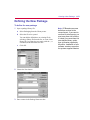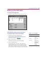
1
MicroSim PCBoards
PC Board Design Software
User’s Guide
MicroSim Corporation
20 Fairbanks
Irvine, California 92618
(714) 770-3022
Version 8.0, June, 1997.
Copyright 1997, MicroSim Corporation. All rights reserved.
Printed in the United States of America.
TradeMarks
Referenced herein are the trademarks used by MicroSim Corporation to identify its products. MicroSim
Corporation is the exclusive owners of “MicroSim,” “PSpice,” “PLogic,” “PLSyn.”
Additional marks of MicroSim include: “StmEd,” “Stimulus Editor,” “Probe,” “Parts,” “Monte Carlo,” “Analog
Behavioral Modeling,” “Device Equations,” “Digital Simulation,” “Digital Files,” “Filter Designer,” “Schematics,”
“PLogic,” ”PCBoards,” “PSpice Optimizer,” and “PLSyn” and variations theron (collectively the “Trademarks”)
are used in connection with computer programs. MicroSim owns various trademark registrations for these marks in
the United States and other countries.
SPECCTRA is a registered trademark of Cooper & Chyan Technology, Inc.
Microsoft, MS-DOS, Windows, Windows NT and the Windows logo are either registered trademarks or trademarks
of Microsoft Corporation.
Adobe, the Adobe logo, Acrobat, the Acrobat logo, Exchange and PostScript are trademarks of Adobe Systems
Incorporated or its subsidiaries and may be registered in certain jurisdictions.
EENET is a trademark of Eckert Enterprises.
All other company/product names are trademarks/registered trademarks of their respective holders.
Copyright Notice
Except as permitted under the United States Copyright Act of 1976, no part of this publication may be reproduced
or distributed in any form or by any means, or stored in a data base or retrieval system, without the prior written
permission of MicroSim Corporation.
As described in the license agreement, you are permitted to run one copy of the MicroSim software on one
computer at a time. Unauthorized duplication of the software or documentation is prohibited by law. Corporate
Program Licensing and multiple copy discounts are available.
Technical Support
Internet
[email protected]
Phone
FAX
WWW
(714) 837-0790
(714) 455-0554
http://www.microsim.com
Customer Service
Internet
Phone
[email protected]
(714) 770-3022
Contents
Before You Begin
Welcome to MicroSim . . . . . . .
MicroSim PCBoards Overview . .
What Is MicroSim PCBoards?
Standard Features . . . . . . .
How to Use this Guide . . . . . . .
Typographical Conventions . .
Related Documentation . . . . . .
Online Help . . . . . . . . . .
What’s New in Release 8 . . . . .
.
.
.
.
.
.
.
.
.
.
.
.
.
.
.
.
.
.
.
.
.
.
.
.
.
.
.
.
.
.
.
.
.
.
.
.
.
.
.
.
.
.
.
.
.
.
.
.
.
.
.
.
.
.
.
.
.
.
.
.
.
.
.
.
.
.
.
.
.
.
.
.
.
.
.
.
.
.
.
.
.
.
.
.
.
.
.
.
.
.
.
.
.
.
.
.
.
.
.
.
.
.
.
.
.
.
.
.
.
.
.
.
.
.
.
.
.
.
.
.
.
.
.
.
.
.
.
.
.
.
.
.
.
.
.
.
.
.
.
.
.
.
.
.
.
.
.
.
.
.
.
.
.
.
.
.
.
.
.
.
.
.
.
.
.
.
.
.
.
.
.
.
.
.
.
.
.
.
.
.
.
.
.
.
.
.
.
.
.
.
.
.
.
.
.
.
.
.
.
.
.
.
.
.
.
.
xix
. xx
. xx
xxi
xxiv
xxiv
xxv
xxvi
xxvii
Overview . . . . . . . . . . . . . . . . . . . . . . . . . . . . . . . .
Layout Editor . . . . . . . . . . . . . . . . . . . . . . . . . . . . .
Configuring the PCBoards Environment . . . . . . . . . . . . .
Initializing and Editing the Design . . . . . . . . . . . . . . . .
Validating the Design . . . . . . . . . . . . . . . . . . . . . . .
Library Editing of Package, Footprint, and Padstack Definitions
Producing Manufacturing Output . . . . . . . . . . . . . . . . .
Layout Database . . . . . . . . . . . . . . . . . . . . . . . . . . . .
The Layout Editor Window . . . . . . . . . . . . . . . . . . . . . .
Menu Bar . . . . . . . . . . . . . . . . . . . . . . . . . . . . .
Toolbar Buttons . . . . . . . . . . . . . . . . . . . . . . . . . .
Toolbar Drop-Down Lists . . . . . . . . . . . . . . . . . . . . .
Work Area . . . . . . . . . . . . . . . . . . . . . . . . . . . . .
Coordinate System . . . . . . . . . . . . . . . . . . . . . .
Grid . . . . . . . . . . . . . . . . . . . . . . . . . . . . . .
Status Bar . . . . . . . . . . . . . . . . . . . . . . . . . . . . .
Cursor Styles . . . . . . . . . . . . . . . . . . . . . . . . . . .
Full-screen crosshair . . . . . . . . . . . . . . . . . . . . .
Selecting Objects . . . . . . . . . . . . . . . . . . . . . . . . . . .
.
.
.
.
.
.
.
.
.
.
.
.
.
.
.
.
.
.
.
.
.
.
.
.
.
.
.
.
.
.
.
.
.
.
.
.
.
.
.
.
.
.
.
.
.
.
.
.
.
.
.
.
.
.
.
.
.
.
.
.
.
.
.
.
.
.
.
.
.
.
.
.
.
.
.
.
. 1-1
. 1-3
. 1-3
. 1-3
. 1-4
. 1-4
. 1-5
. 1-6
. 1-7
. 1-7
. 1-8
. 1-9
. 1-11
. 1-11
. 1-11
. 1-11
. 1-12
. 1-12
. 1-14
Chapter 1 Using the Layout Editor
iv Contents
Selecting Objects One at a Time . . . . . . . .
Selecting Groups of Objects . . . . . . . . . .
Using the Selection Filter . . . . . . . . . . .
Using the Find Command . . . . . . . . . . .
Using the Keyboard . . . . . . . . . . . . . . . .
Changing Views . . . . . . . . . . . . . . . . . .
Panning . . . . . . . . . . . . . . . . . . . . .
Zooming . . . . . . . . . . . . . . . . . . . .
Redrawing the Display . . . . . . . . . . . . .
Defining, Modifying, and Deleting Styles . . . . .
Line and Arc Styles . . . . . . . . . . . . . .
Text Styles . . . . . . . . . . . . . . . . . . .
To Delete . . . . . . . . . . . . . . . . .
Trace Styles . . . . . . . . . . . . . . . . . .
To Define or Modify . . . . . . . . . . .
To Delete . . . . . . . . . . . . . . . . .
Padstack Styles . . . . . . . . . . . . . . . . .
Adding and Changing
Object Attributes . . . . . . . . . . . . .
Adding Attributes . . . . . . . . . . . . . . .
Changing Attribute Values . . . . . . . . . . .
Changing the Display Parameters of Attributes
Using the Message Viewer . . . . . . . . . . . . .
Using Online Help . . . . . . . . . . . . . . .
Locating the Source of a Message . . . . . . .
Understanding the Indicated Severity . . . . .
Additional Information . . . . . . . . . . . .
Closing the Message Viewer . . . . . . . . . .
Using Design Rule Check (DRC) . . . . . . . . .
.
.
.
.
.
.
.
.
.
.
.
.
.
.
.
.
.
.
.
.
.
.
.
.
.
.
.
.
.
.
.
.
.
.
.
.
.
.
.
.
.
.
.
.
.
.
.
.
.
.
.
.
.
.
.
.
.
.
.
.
.
.
.
.
.
.
.
.
.
.
.
.
.
.
.
.
.
.
.
.
.
.
.
.
.
.
.
.
.
.
.
.
.
.
.
.
.
.
.
.
.
.
.
.
.
.
.
.
.
.
.
.
.
.
.
.
.
.
.
.
.
.
.
.
.
.
.
.
.
.
.
.
.
.
.
.
.
.
.
.
.
.
.
.
.
.
.
.
.
.
.
.
.
.
.
.
.
.
.
.
.
.
.
.
.
.
.
.
.
.
.
.
.
.
.
.
.
.
.
.
.
.
.
.
.
.
.
.
.
.
.
.
.
.
.
.
.
.
.
.
.
.
.
.
.
.
.
.
.
.
.
.
.
.
.
.
.
.
.
.
.
.
.
.
.
.
.
.
.
.
.
.
.
.
.
.
.
.
1-14
1-14
1-15
1-17
1-18
1-19
1-19
1-20
1-21
1-24
1-24
1-25
1-26
1-27
1-27
1-29
1-29
.
.
.
.
.
.
.
.
.
.
.
.
.
.
.
.
.
.
.
.
.
.
.
.
.
.
.
.
.
.
.
.
.
.
.
.
.
.
.
.
.
.
.
.
.
.
.
.
.
.
.
.
.
.
.
.
.
.
.
.
.
.
.
.
.
.
.
.
.
.
.
.
.
.
.
.
.
.
.
.
.
.
.
.
.
.
.
.
.
.
.
.
.
.
.
.
.
.
.
.
.
.
.
.
.
.
.
.
.
.
.
.
.
.
.
.
.
.
.
.
.
.
.
.
.
.
.
.
.
.
.
.
.
.
.
.
.
.
.
.
.
.
.
.
.
.
.
.
.
.
.
.
.
.
1-30
1-30
1-31
1-31
1-33
1-33
1-34
1-34
1-34
1-36
1-37
Overview . . . . . . . . . . . . . . . . . . . . . . . . .
Starting the Layout Editor . . . . . . . . . . . . . . . .
Opening Additional Layouts . . . . . . . . . . . . .
Starting a New Layout . . . . . . . . . . . . . . . . . .
Loading a Netlist . . . . . . . . . . . . . . . . . . .
Importing a Netlist from MicroSim Schematics
Importing a PADS format netlist . . . . . . . .
Using Interactive Netlist Readin . . . . . . . .
Modifying an Existing Layout . . . . . . . . . . . .
Creating a Layout On-the-Fly . . . . . . . . . . . .
.
.
.
.
.
.
.
.
.
.
.
.
.
.
.
.
.
.
.
.
.
.
.
.
.
.
.
.
.
.
.
.
.
.
.
.
.
.
.
.
.
.
.
.
.
.
.
.
.
.
.
.
.
.
.
.
.
.
.
.
.
.
.
.
.
.
.
.
.
.
.
.
.
.
.
.
.
.
.
.
.
.
.
.
.
.
.
.
.
.
.
.
.
.
.
.
.
.
.
.
.
.
.
.
.
.
.
.
.
.
Chapter 2 Starting a New Layout
.
.
.
.
.
.
.
.
.
.
2-1
2-3
2-3
2-4
2-4
2-5
2-6
2-6
2-9
2-9
Contents
v
Saving Your Layout Automatically . . . . . . . . . . . . . . . . . . . . . . . 2-10
Hints and Tips . . . . . . . . . . . . . . . . . . . . . . . . . . . . . . . . . . 2-11
Chapter 3 Defining the Circuit Board
Overview . . . . . . . . . . . . . . . . . . .
Setting the Unit of Measure . . . . . . . . .
Setting Styles . . . . . . . . . . . . . . . .
Line and Arc Styles . . . . . . . . . . .
Text Styles . . . . . . . . . . . . . . . .
Defining Grids . . . . . . . . . . . . . . . .
Setting the Spacing . . . . . . . . . . .
Turning On the Snap Grid . . . . . . . .
Displaying the Grid . . . . . . . . . . .
Graphic Objects . . . . . . . . . . . . . . .
Arc . . . . . . . . . . . . . . . . . . . .
Circle . . . . . . . . . . . . . . . . . .
Line . . . . . . . . . . . . . . . . . . .
Polyline . . . . . . . . . . . . . . . . .
Rectangle . . . . . . . . . . . . . . . .
More Graphics . . . . . . . . . . . . . .
Arc-Thru 3 points . . . . . . . . . .
Arc-coord. & radius . . . . . . . . .
Arc-center & radius . . . . . . . . .
Line-coord . . . . . . . . . . . . .
Rect.-coord. . . . . . . . . . . . . .
Rect.-coord. & deltas . . . . . . . .
Rect.-corner & deltas . . . . . . . .
Text Objects . . . . . . . . . . . . . . . . .
Adding Text . . . . . . . . . . . . . . .
Creating the Board Outline . . . . . . . . .
Drawing the Board Outline . . . . . . .
Importing a DXF File . . . . . . . . . .
Layer control and association . . . .
Entity Considerations . . . . . . . .
Text . . . . . . . . . . . . . . . . .
Messages . . . . . . . . . . . . . .
Adding Holes . . . . . . . . . . . . . . . .
Adding Unplated Holes . . . . . . . . .
Adding Plated Holes . . . . . . . . . .
Drawing a Board Signal Keepin . . . . . . .
Editing a Board Signal Keepin Boundary
.
.
.
.
.
.
.
.
.
.
.
.
.
.
.
.
.
.
.
.
.
.
.
.
.
.
.
.
.
.
.
.
.
.
.
.
.
.
.
.
.
.
.
.
.
.
.
.
.
.
.
.
.
.
.
.
.
.
.
.
.
.
.
.
.
.
.
.
.
.
.
.
.
.
.
.
.
.
.
.
.
.
.
.
.
.
.
.
.
.
.
.
.
.
.
.
.
.
.
.
.
.
.
.
.
.
.
.
.
.
.
.
.
.
.
.
.
.
.
.
.
.
.
.
.
.
.
.
.
.
.
.
.
.
.
.
.
.
.
.
.
.
.
.
.
.
.
.
.
.
.
.
.
.
.
.
.
.
.
.
.
.
.
.
.
.
.
.
.
.
.
.
.
.
.
.
.
.
.
.
.
.
.
.
.
.
.
.
.
.
.
.
.
.
.
.
.
.
.
.
.
.
.
.
.
.
.
.
.
.
.
.
.
.
.
.
.
.
.
.
.
.
.
.
.
.
.
.
.
.
.
.
.
.
.
.
.
.
.
.
.
.
.
.
.
.
.
.
.
.
.
.
.
.
.
.
.
.
.
.
.
.
.
.
.
.
.
.
.
.
.
.
.
.
.
.
.
.
.
.
.
.
.
.
.
.
.
.
.
.
.
.
.
.
.
.
.
.
.
.
.
.
.
.
.
.
.
.
.
.
.
.
.
.
.
.
.
.
.
.
.
.
.
.
.
.
.
.
.
.
.
.
.
.
.
.
.
.
.
.
.
.
.
.
.
.
.
.
.
.
.
.
.
.
.
.
.
.
.
.
.
.
.
.
.
.
.
.
.
.
.
.
.
.
.
.
.
.
.
.
.
.
.
.
.
.
.
.
.
.
.
.
.
.
.
.
.
.
.
.
.
.
.
.
.
.
.
.
.
.
.
.
.
.
.
.
.
.
.
.
.
.
.
.
.
.
.
.
.
.
.
.
.
.
.
.
.
.
.
.
.
.
.
.
.
.
.
.
.
.
.
.
.
.
.
.
.
.
.
.
.
.
.
.
.
.
.
.
.
.
.
.
.
.
.
.
.
.
.
.
.
.
.
.
.
.
.
.
.
.
.
.
.
.
.
.
.
.
.
.
.
.
.
.
.
.
.
.
.
.
.
.
.
.
.
.
.
.
.
.
.
.
.
.
.
.
.
.
.
.
.
.
.
.
.
.
.
.
.
.
.
.
.
.
.
.
.
.
.
.
.
.
.
.
.
.
.
.
.
.
.
.
.
.
.
.
.
.
.
.
.
.
.
.
.
.
.
.
.
.
.
.
.
.
.
.
.
.
.
.
.
.
.
.
.
.
.
.
.
.
.
.
.
.
.
.
.
.
.
.
.
.
.
.
.
.
.
.
.
.
.
.
.
.
.
.
.
.
.
. 3-1
. 3-3
. 3-4
. 3-4
. 3-4
. 3-6
. 3-6
. 3-7
. 3-8
. 3-9
. 3-9
. 3-10
. 3-10
. 3-11
. 3-12
. 3-12
. 3-12
. 3-13
. 3-13
. 3-14
. 3-15
. 3-15
. 3-16
. 3-17
. 3-17
. 3-18
. 3-18
. 3-18
. 3-18
. 3-19
. 3-20
. 3-21
. 3-24
. 3-24
. 3-24
. 3-25
. 3-25
vi Contents
Configuring Layers . . . . . . . . . . . . .
Layer Types . . . . . . . . . . . . . .
Signal Layers . . . . . . . . . . .
Graphic layers . . . . . . . . . . .
Layer Tag Assignments . . . . . . . .
Layer Properties . . . . . . . . . . . .
Layer Pairs . . . . . . . . . . . . . . .
Creating a User-Defined Layer . . . .
Editing an Existing Layer . . . . . . .
Repositioning User-Defined Layers
Deleting a User-Defined Layer . . . .
Creating a Layer Pair . . . . . . . . .
Deleting a Layer Pair . . . . . . . . .
Changing the Layer Display . . . . . . . .
Turning Specific Layers On . . . . . .
Changing Layer Color . . . . . . . . .
Making a Layer Current . . . . . . . .
Hints and Tips . . . . . . . . . . . . . . .
.
.
.
.
.
.
.
.
.
.
.
.
.
.
.
.
.
.
.
.
.
.
.
.
.
.
.
.
.
.
.
.
.
.
.
.
.
.
.
.
.
.
.
.
.
.
.
.
.
.
.
.
.
.
.
.
.
.
.
.
.
.
.
.
.
.
.
.
.
.
.
.
.
.
.
.
.
.
.
.
.
.
.
.
.
.
.
.
.
.
.
.
.
.
.
.
.
.
.
.
.
.
.
.
.
.
.
.
.
.
.
.
.
.
.
.
.
.
.
.
.
.
.
.
.
.
.
.
.
.
.
.
.
.
.
.
.
.
.
.
.
.
.
.
.
.
.
.
.
.
.
.
.
.
.
.
.
.
.
.
.
.
.
.
.
.
.
.
.
.
.
.
.
.
.
.
.
.
.
.
.
.
.
.
.
.
.
.
.
.
.
.
.
.
.
.
.
.
.
.
.
.
.
.
.
.
.
.
.
.
.
.
.
.
.
.
.
.
.
.
.
.
.
.
.
.
.
.
.
.
.
.
.
.
.
.
.
.
.
.
.
.
.
.
.
.
.
.
.
.
.
.
.
.
.
.
.
.
.
.
.
.
.
.
.
.
.
.
.
.
.
.
.
.
.
.
.
.
.
.
.
.
.
.
.
.
.
.
.
.
.
.
.
.
.
.
.
.
.
.
.
.
.
.
.
.
.
.
.
.
.
.
.
.
.
.
.
.
.
.
.
.
.
.
Overview . . . . . . . . . . . . . . . . . . . . . . . .
Understanding Connectivity . . . . . . . . . . . . . .
Logical Connections . . . . . . . . . . . . . . . .
Rats and ratsnests . . . . . . . . . . . . . . .
Physical Connections . . . . . . . . . . . . . . .
Nets . . . . . . . . . . . . . . . . . . . . . . . .
Floating copper . . . . . . . . . . . . . . . .
Managing Rats . . . . . . . . . . . . . . . . . . . . .
Optimizing Rats . . . . . . . . . . . . . . . . . .
Changing the Ratsnest Display . . . . . . . . . .
Cross Probing . . . . . . . . . . . . . . . . . . . . .
Moving Objects . . . . . . . . . . . . . . . . . . . .
Changing Object Orientation . . . . . . . . . . .
Moving Components . . . . . . . . . . . . . . . .
Moving components by delta values . . . . .
Moving Components by Reference Designator
Adding Components . . . . . . . . . . . . . . . . . .
Cutting, Copying, and Pasting Components . . . . . .
Cutting Components . . . . . . . . . . . . . . . .
Copying Components . . . . . . . . . . . . . . .
Pasting Components . . . . . . . . . . . . . . . .
.
.
.
.
.
.
.
.
.
.
.
.
.
.
.
.
.
.
.
.
.
.
.
.
.
.
.
.
.
.
.
.
.
.
.
.
.
.
.
.
.
.
.
.
.
.
.
.
.
.
.
.
.
.
.
.
.
.
.
.
.
.
.
.
.
.
.
.
.
.
.
.
.
.
.
.
.
.
.
.
.
.
.
.
.
.
.
.
.
.
.
.
.
.
.
.
.
.
.
.
.
.
.
.
.
.
.
.
.
.
.
.
.
.
.
.
.
.
.
.
.
.
.
.
.
.
.
.
.
.
.
.
.
.
.
.
.
.
.
.
.
.
.
.
.
.
.
.
.
.
.
.
.
.
.
.
.
.
.
.
.
.
.
.
.
.
.
.
.
.
.
.
.
.
.
.
.
.
.
.
.
.
.
.
.
.
.
.
.
.
.
.
.
.
.
.
.
.
.
.
.
.
.
.
.
.
.
.
.
.
.
.
.
.
.
.
.
.
.
.
.
.
.
.
.
.
.
.
.
.
.
.
.
.
.
.
.
.
.
.
.
.
.
.
.
.
.
.
.
.
.
.
3-28
3-28
3-28
3-29
3-29
3-32
3-33
3-35
3-37
3-38
3-38
3-39
3-40
3-41
3-41
3-42
3-42
3-43
Chapter 4 Arranging Components
.
.
.
.
.
.
.
.
.
.
4-1
4-3
4-3
4-3
4-4
4-5
4-6
4-8
4-8
4-9
4-11
4-12
4-12
4-13
4-13
4-14
4-15
4-18
4-18
4-18
4-19
Contents vii
Deleting Components
Adding Connections .
Deleting Connections
Hints and Tips . . . .
.
.
.
.
.
.
.
.
.
.
.
.
.
.
.
.
.
.
.
.
.
.
.
.
.
.
.
.
.
.
.
.
.
.
.
.
.
.
.
.
.
.
.
.
.
.
.
.
.
.
.
.
.
.
.
.
.
.
.
.
.
.
.
.
.
.
.
.
.
.
.
.
.
.
.
.
.
.
.
.
.
.
.
.
.
.
.
.
.
.
.
.
.
.
.
.
.
.
.
.
.
.
.
.
.
.
.
.
.
.
.
.
.
.
.
.
. 4-20
. 4-21
. 4-22
. 4-23
Overview . . . . . . . . . . . . . . . . . . . . .
Modifying the Layer Configuration . . . . . . .
Creating a User-Defined Layer . . . . . . .
Editing an Existing Layer . . . . . . . . . .
Repositioning User-Defined Layers . .
Deleting a User-Defined Layer . . . . . . .
Creating a Layer Pair . . . . . . . . . . . .
Deleting a Layer Pair . . . . . . . . . . . .
Drawing and Editing Areafills for Plane Layers
Drawing Areafills . . . . . . . . . . . . . .
Specifying the areafill net . . . . . . . .
Editing Areafill Attributes . . . . . . . . . .
Editing areafill boundaries . . . . . . .
Thermal relief . . . . . . . . . . . . . .
Creating Plane Layers . . . . . . . . . . . .
Adding a Keepout . . . . . . . . . . . . . . . .
Editing a Keepout Boundary . . . . . . . .
Using Design Rule Check (DRC) . . . . . . . .
Electrical Rules Handling . . . . . . . . . .
Setting minimum manufacturing values
Setting Clearance Values . . . . . . . . . .
Setting trace segment clearances . . . .
Setting areafill clearances . . . . . . . .
Setting pad clearances . . . . . . . . .
Using Online DRC . . . . . . . . . . . . .
Using Batch DRC . . . . . . . . . . . . . .
.
.
.
.
.
.
.
.
.
.
.
.
.
.
.
.
.
.
.
.
.
.
.
.
.
.
.
.
.
.
.
.
.
.
.
.
.
.
.
.
.
.
.
.
.
.
.
.
.
.
.
.
.
.
.
.
.
.
.
.
.
.
.
.
.
.
.
.
.
.
.
.
.
.
.
.
.
.
.
.
.
.
.
.
.
.
.
.
.
.
.
.
.
.
.
.
.
.
.
.
.
.
.
.
.
.
.
.
.
.
.
.
.
.
.
.
.
.
.
.
.
.
.
.
.
.
.
.
.
.
.
.
.
.
.
.
.
.
.
.
.
.
.
.
.
.
.
.
.
.
.
.
.
.
.
.
.
.
.
.
.
.
.
.
.
.
.
.
.
.
.
.
.
.
.
.
.
.
.
.
.
.
.
.
.
.
.
.
.
.
.
.
.
.
.
.
.
.
.
.
.
.
.
.
.
.
.
.
.
.
.
.
.
.
.
.
.
.
.
.
.
.
.
.
.
.
.
.
.
.
.
.
.
.
.
.
.
.
.
.
.
.
.
.
.
.
.
.
.
.
.
.
.
.
.
.
.
.
.
.
.
.
.
.
.
.
.
.
.
.
.
.
.
.
.
.
.
.
.
.
.
.
.
.
.
.
.
.
.
.
.
.
.
.
.
.
.
.
.
.
.
.
.
.
.
.
.
.
.
.
.
.
.
.
.
.
.
.
.
.
.
.
.
.
.
.
.
.
.
.
.
.
.
.
.
.
.
.
.
.
.
.
.
.
.
.
.
.
.
.
.
.
.
.
.
.
.
.
.
.
.
.
.
.
.
.
.
.
.
.
.
.
.
.
.
.
.
.
.
.
.
.
.
.
.
.
.
.
.
.
. 5-1
. 5-2
. 5-2
. 5-4
. 5-5
. 5-6
. 5-6
. 5-7
. 5-8
. 5-8
. 5-9
. 5-9
. 5-11
. 5-13
. 5-13
. 5-15
. 5-15
. 5-16
. 5-16
. 5-16
. 5-17
. 5-18
. 5-18
. 5-19
. 5-20
. 5-21
.
.
.
.
.
.
.
.
.
.
.
.
.
.
.
.
.
.
.
.
.
.
.
.
.
.
.
.
.
.
.
.
.
.
.
.
.
.
.
.
.
.
.
.
.
.
.
.
.
.
.
.
.
.
.
.
.
.
.
.
.
.
.
.
.
.
.
.
.
.
.
.
.
.
.
.
.
.
.
.
.
.
.
.
.
.
.
.
.
.
.
.
.
.
.
.
.
.
.
.
.
.
.
.
.
.
.
.
.
.
.
.
Chapter 5 Preparing the Layout for Routing
Chapter 6 Routing Interactively
Overview . . . . . . . . . . . .
Highlighting Nets . . . . . . .
Selecting the Net(s) First .
Selecting the Net(s) Last .
Clearing Highlighted Nets .
Routing Traces . . . . . . . . .
Trace Placement Mode . .
.
.
.
.
.
.
.
.
.
.
.
.
.
.
.
.
.
.
.
.
.
.
.
.
.
.
.
.
.
.
.
.
.
.
.
.
.
.
.
.
.
.
.
.
.
.
.
.
.
.
.
.
.
.
.
.
.
.
.
.
.
.
.
6-1
6-3
6-3
6-3
6-4
6-5
6-7
viii Contents
Understanding the Smart Functions .
Understanding Smart Snap . . . .
Snap threshold . . . . . . . .
Using Automatic Loop Removal
Understanding Smart Select . . .
Understanding Smart Move . . .
Understanding Pins and Vias . . . . .
Pins . . . . . . . . . . . . . . . .
Vias . . . . . . . . . . . . . . .
Placing a via . . . . . . . . .
Working with Areafills . . . . . . . .
SMT Considerations . . . . . . .
Split Power and Grounds . . . .
Voids . . . . . . . . . . . . . . .
Editing void boundaries . . .
Islands . . . . . . . . . . . . . .
Automatic Spoke Removal . . .
Hints and Tips . . . . . . . . . . . .
.
.
.
.
.
.
.
.
.
.
.
.
.
.
.
.
.
.
.
.
.
.
.
.
.
.
.
.
.
.
.
.
.
.
.
.
.
.
.
.
.
.
.
.
.
.
.
.
.
.
.
.
.
.
.
.
.
.
.
.
.
.
.
.
.
.
.
.
.
.
.
.
.
.
.
.
.
.
.
.
.
.
.
.
.
.
.
.
.
.
.
.
.
.
.
.
.
.
.
.
.
.
.
.
.
.
.
.
.
.
.
.
.
.
.
.
.
.
.
.
.
.
.
.
.
.
.
.
.
.
.
.
.
.
.
.
.
.
.
.
.
.
.
.
.
.
.
.
.
.
.
.
.
.
.
.
.
.
.
.
.
.
.
.
.
.
.
.
.
.
.
.
.
.
.
.
.
.
.
.
.
.
.
.
.
.
.
.
.
.
.
.
.
.
.
.
.
.
.
.
.
.
.
.
.
.
.
.
.
.
.
.
.
.
.
.
.
.
.
.
.
.
.
.
.
.
.
.
.
.
.
.
.
.
.
.
.
.
.
.
.
.
.
.
.
.
.
.
.
.
.
.
.
.
.
.
.
.
.
.
.
.
.
.
.
.
.
.
.
.
.
.
.
.
.
.
.
.
.
.
.
.
.
.
.
.
.
.
.
.
.
.
.
.
.
.
.
.
.
.
.
.
.
.
.
.
.
.
.
.
.
.
.
.
.
.
.
.
.
.
.
.
.
.
.
.
.
.
.
.
.
.
.
.
.
.
.
.
.
.
.
.
.
.
.
.
.
.
.
.
.
.
.
.
.
.
.
.
.
.
.
.
.
.
.
.
.
.
.
.
.
.
.
.
.
.
.
.
. 6-8
. 6-8
6-10
6-11
6-12
6-13
6-16
6-16
6-16
6-17
6-19
6-19
6-19
6-20
6-20
6-23
6-24
6-25
Chapter 7 Routing with the CCT SPECCTRA Autorouter
Overview . . . . . . . . . . . . . . . . . . .
Setting up for Autorouting . . . . . . . . . .
Verifying Advanced Net Rules . . . . . . . .
Starting the Autorouter . . . . . . . . . . . .
Reading the route file automatically .
Reading the route file interactively .
Hints and Tips . . . . . . . . . . . . . . . .
.
.
.
.
.
.
.
.
.
.
.
.
.
.
.
.
.
.
.
.
.
.
.
.
.
.
.
.
.
.
.
.
.
.
.
.
.
.
.
.
.
.
.
.
.
.
.
.
.
.
.
.
.
.
.
.
.
.
.
.
.
.
.
.
.
.
.
.
.
.
.
.
.
.
.
.
.
.
.
.
.
.
.
.
.
.
.
.
.
.
.
.
.
.
.
.
.
.
.
.
.
.
.
.
.
.
.
.
.
.
.
.
.
.
.
.
.
.
.
.
.
.
.
.
.
7-1
7-3
7-6
7-8
7-8
7-9
7-10
.
.
.
.
.
.
.
.
.
.
.
.
.
.
.
.
.
.
.
.
.
.
.
.
.
.
.
.
.
.
.
.
.
.
.
.
.
.
.
.
.
.
.
.
.
.
.
.
.
.
.
.
.
.
.
.
.
.
.
.
.
.
.
.
.
.
.
.
.
.
.
.
.
.
.
.
.
.
.
.
.
.
.
.
.
.
.
.
.
.
.
.
.
.
.
.
.
.
.
.
.
.
.
.
.
.
.
.
.
.
.
.
.
.
.
.
.
.
.
.
.
.
.
.
.
.
.
.
.
.
.
.
.
.
.
.
.
.
.
.
.
.
.
.
.
.
.
.
.
.
.
.
.
.
.
.
.
.
.
.
.
.
.
.
.
.
.
.
.
.
.
.
.
.
.
.
.
.
.
.
.
.
.
.
.
.
.
.
.
.
.
.
.
.
.
.
.
.
.
.
.
.
.
.
.
.
.
.
.
.
.
.
8-1
8-2
8-2
8-4
8-5
8-6
8-7
8-8
8-11
8-11
8-11
8-12
Chapter 8 Editing Traces
Overview . . . . . . . . . . . . . . .
Understanding the Smart Functions .
Understanding Smart Snap . . . .
Snap threshold . . . . . . . .
Using Automatic Loop Removal
Understanding Smart Select . . .
Understanding Rubberbanding .
Understanding Smart Move . . .
Cutting, Copying, and Pasting Traces
Cutting Traces . . . . . . . . . .
Copying traces . . . . . . . . . .
Pasting traces . . . . . . . . . . .
.
.
.
.
.
.
.
.
.
.
.
.
.
.
.
.
.
.
.
.
.
.
.
.
.
.
.
.
.
.
.
.
.
.
.
.
.
.
.
.
.
.
.
.
.
.
.
.
Contents ix
Deleting Trace Segments and Vias
Adding Connections . . . . . . . .
Deleting Connections . . . . . . .
Hints and Tips . . . . . . . . . . .
.
.
.
.
.
.
.
.
.
.
.
.
.
.
.
.
.
.
.
.
.
.
.
.
.
.
.
.
.
.
.
.
.
.
.
.
.
.
.
.
.
.
.
.
.
.
.
.
.
.
.
.
.
.
.
.
.
.
.
.
.
.
.
.
.
.
.
.
.
.
.
.
.
.
.
.
.
.
.
.
.
.
.
.
.
.
.
.
. 8-13
. 8-14
. 8-16
. 8-17
Chapter 9 Creating and Editing Pin and Via Padstacks
Overview . . . . . . . . . . . . . . . . . . . . . . .
Understanding Padstack Definitions . . . . . . . . .
Understanding the Library Structure . . . . . . . .
Library Definitions . . . . . . . . . . . . . . .
Managing Padstack Libraries . . . . . . . . . . . .
Setting Up the Padstack Library . . . . . . . .
Loading Padstacks . . . . . . . . . . . . . . . .
Exporting Padstacks . . . . . . . . . . . . . . .
Creating Padstacks . . . . . . . . . . . . . . . . . .
Beginning the Definition . . . . . . . . . . . .
Assigning Default Properties . . . . . . . . . .
Defining Drill Parameters . . . . . . . . . . . .
Defining Mask Properties . . . . . . . . . . . .
Removing Non-Functional Pads on Inner Layers
Saving the Definition . . . . . . . . . . . . . .
Editing Padstacks . . . . . . . . . . . . . . . . . .
Deleting Padstacks . . . . . . . . . . . . . . . . . .
Changing Padstack Assignments . . . . . . . . . .
Hints and Tips . . . . . . . . . . . . . . . . . . . .
.
.
.
.
.
.
.
.
.
.
.
.
.
.
.
.
.
.
.
.
.
.
.
.
.
.
.
.
.
.
.
.
.
.
.
.
.
.
.
.
.
.
.
.
.
.
.
.
.
.
.
.
.
.
.
.
.
.
.
.
.
.
.
.
.
.
.
.
.
.
.
.
.
.
.
.
.
.
.
.
.
.
.
.
.
.
.
.
.
.
.
.
.
.
.
.
.
.
.
.
.
.
.
.
.
.
.
.
.
.
.
.
.
.
.
.
.
.
.
.
.
.
.
.
.
.
.
.
.
.
.
.
.
.
.
.
.
.
.
.
.
.
.
.
.
.
.
.
.
.
.
.
.
.
.
.
.
.
.
.
.
.
.
.
.
.
.
.
.
.
.
.
.
.
.
.
.
.
.
.
.
.
.
.
.
.
.
.
.
.
.
.
.
.
.
.
.
.
.
.
.
.
.
.
.
.
.
.
.
.
.
.
.
.
.
.
.
.
.
.
.
.
.
.
.
.
.
.
.
.
.
.
.
.
.
.
.
.
.
.
.
.
.
.
.
.
.
. 9-1
. 9-3
. 9-4
. 9-5
. 9-7
. 9-7
. 9-8
. 9-9
. 9-10
. 9-11
. 9-12
. 9-14
. 9-15
. 9-15
. 9-16
. 9-17
. 9-18
. 9-19
. 9-20
.
.
.
.
.
.
.
.
.
.
.
.
.
.
.
.
.
.
.
.
.
.
.
.
.
.
.
.
.
.
.
.
.
.
.
.
.
.
.
.
.
.
.
.
.
.
.
.
.
.
.
.
.
.
.
.
.
.
.
.
.
.
.
.
.
.
.
.
.
.
.
.
.
.
.
.
.
.
.
.
.
.
.
.
.
.
.
.
.
.
.
.
.
.
.
.
.
.
.
.
.
.
.
.
.
.
.
.
.
.
.
.
.
.
.
.
.
.
.
.
.
.
.
.
.
.
.
.
.
.
.
.
.
.
.
.
.
.
.
.
.
.
.
.
.
.
.
.
.
.
.
.
.
.
.
.
.
.
.
.
.
.
.
.
.
.
.
.
.
.
.
.
.
.
.
.
.
.
.
.
.
.
. 10-1
. 10-3
. 10-3
. 10-5
. 10-5
. 10-7
. 10-8
. 10-8
. 10-9
10-10
10-10
10-11
10-11
10-12
Chapter 10 Creating and Editing Footprints
Overview . . . . . . . . . . . . . . . . . . . . .
Understanding the Library Structure . . . . . .
Library Definitions . . . . . . . . . . . . .
Managing Footprint Library Files . . . . . . . .
Adding a Footprint Library . . . . . . . . .
Rearranging the Search Order . . . . . . . .
Creating a New Footprint . . . . . . . . . . . .
Starting the Footprint Editor . . . . . . . .
Setting the Name of the Footprint Definition
Setting Unit of Measure . . . . . . . . . . .
Setting Grid Spacing . . . . . . . . . . . .
Turning the Snap Grid On . . . . . . . . . .
Displaying the Grid . . . . . . . . . . . . .
Assigning a Padstack . . . . . . . . . . . .
.
.
.
.
.
.
.
.
.
.
.
.
.
.
.
.
.
.
.
.
.
.
.
.
.
.
.
.
x Contents
Drawing Pins . . . . . . . . . . . . . . . . . . . . . . . . . . . . . . .
Drawing pins individually or automatically . . . . . . . . . . . . .
Drawing pin arrays . . . . . . . . . . . . . . . . . . . . . . . . .
Drawing radial pins . . . . . . . . . . . . . . . . . . . . . . . . .
Drawing the Part Outline . . . . . . . . . . . . . . . . . . . . . . . .
Marking the Footprint Orientation . . . . . . . . . . . . . . . . . . . .
Identifying the Footprint Origin . . . . . . . . . . . . . . . . . . . . .
Drawing the Footprint Boundary . . . . . . . . . . . . . . . . . . . .
Identifying the Machine Placement Center . . . . . . . . . . . . . . .
Defining the Reference Designator and Component Type_Name Style
Setting text styles . . . . . . . . . . . . . . . . . . . . . . . . . .
Positioning the templates . . . . . . . . . . . . . . . . . . . . . .
Changing Pin-Padstack Assignments . . . . . . . . . . . . . . . . . .
Adding Holes . . . . . . . . . . . . . . . . . . . . . . . . . . . . . .
Adding unplated holes . . . . . . . . . . . . . . . . . . . . . . . .
Adding plated holes . . . . . . . . . . . . . . . . . . . . . . . . .
Saving the Footprint Definition to a Footprint Library File . . . . . . .
Editing an Existing Footprint . . . . . . . . . . . . . . . . . . . . . . . .
Copying Footprints . . . . . . . . . . . . . . . . . . . . . . . . . . . . . .
Removing Footprints . . . . . . . . . . . . . . . . . . . . . . . . . . . . .
Printing the Footprint . . . . . . . . . . . . . . . . . . . . . . . . . . . . .
Updating Placed Footprints . . . . . . . . . . . . . . . . . . . . . . . . .
Changing Footprint Assignments . . . . . . . . . . . . . . . . . . . . . .
Hints and Tips . . . . . . . . . . . . . . . . . . . . . . . . . . . . . . . .
.
.
.
.
.
.
.
.
.
.
.
.
.
.
.
.
.
.
.
.
.
.
.
.
10-12
10-13
10-14
10-17
10-18
10-18
10-19
10-19
10-22
10-23
10-23
10-25
10-26
10-27
10-28
10-28
10-28
10-30
10-32
10-34
10-35
10-37
10-38
10-39
.
.
.
.
.
.
.
.
.
.
.
.
.
.
.
11-1
11-3
11-3
11-5
11-5
11-7
11-8
11-8
11-9
11-10
11-12
11-13
11-14
11-16
11-17
Chapter 11 Creating and Editing Packages
Overview . . . . . . . . . . . . . . . . . . . . .
Understanding the Library Structure . . . . . . .
Library Definitions . . . . . . . . . . . . . .
Managing Package Libraries . . . . . . . . . . .
Adding a Package Library . . . . . . . . . .
Rearranging the Search Order . . . . . . . .
Creating a New Package . . . . . . . . . . . . .
Checking the MicroSim Footprint Library .
Defining the New Package . . . . . . . . . .
Specifying package definition properties
Saving the definition . . . . . . . . . . .
Creating AKO Package Definitions . . . . .
Editing an AKO Package Definition . . . . .
Editing a Package Definition . . . . . . . . . . .
Hints and Tips . . . . . . . . . . . . . . . . . .
.
.
.
.
.
.
.
.
.
.
.
.
.
.
.
.
.
.
.
.
.
.
.
.
.
.
.
.
.
.
.
.
.
.
.
.
.
.
.
.
.
.
.
.
.
.
.
.
.
.
.
.
.
.
.
.
.
.
.
.
.
.
.
.
.
.
.
.
.
.
.
.
.
.
.
.
.
.
.
.
.
.
.
.
.
.
.
.
.
.
.
.
.
.
.
.
.
.
.
.
.
.
.
.
.
.
.
.
.
.
.
.
.
.
.
.
.
.
.
.
.
.
.
.
.
.
.
.
.
.
.
.
.
.
.
.
.
.
.
.
.
.
.
.
.
.
.
.
.
.
.
.
.
.
.
.
.
.
.
.
.
.
.
.
.
.
.
.
.
.
.
.
.
.
.
.
.
.
.
.
.
.
.
.
.
.
.
.
.
.
.
.
.
.
.
.
.
.
.
.
.
.
.
.
.
.
.
.
.
.
Contents xi
Chapter 12 Applying Forward and Backward ECOs
Overview . . . . . . . . . . . . .
Understanding the ECO Process .
Working with Backward ECOs .
.bco File . . . . . . . . . . .
.blg Log File . . . . . . . . .
Applying Backward ECOs .
Working with Forward ECOs . .
.flg Log File . . . . . . . . .
Applying Forward ECOs . .
Comparing Netlists . . . . . . .
Hints and Tips . . . . . . . . . .
.
.
.
.
.
.
.
.
.
.
.
.
.
.
.
.
.
.
.
.
.
.
.
.
.
.
.
.
.
.
.
.
.
.
.
.
.
.
.
.
.
.
.
.
.
.
.
.
.
.
.
.
.
.
.
.
.
.
.
.
.
.
.
.
.
.
.
.
.
.
.
.
.
.
.
.
.
.
.
.
.
.
.
.
.
.
.
.
.
.
.
.
.
.
.
.
.
.
.
.
.
.
.
.
.
.
.
.
.
.
.
.
.
.
.
.
.
.
.
.
.
.
.
.
.
.
.
.
.
.
.
.
.
.
.
.
.
.
.
.
.
.
.
.
.
.
.
.
.
.
.
.
.
.
.
.
.
.
.
.
.
.
.
.
.
.
.
.
.
.
.
.
.
.
.
.
.
.
.
.
.
.
.
.
.
.
.
.
.
.
.
.
.
.
.
.
.
.
.
.
.
.
.
.
.
.
.
.
.
.
.
.
.
.
.
.
.
.
.
.
.
.
.
.
.
.
.
.
.
.
.
.
.
.
.
.
.
.
.
.
.
.
.
.
.
.
.
.
.
.
.
.
.
. 12-1
. 12-2
. 12-4
. 12-4
. 12-4
. 12-5
. 12-7
. 12-7
. 12-7
12-10
12-12
Overview . . . . . . . . . . . . . . . . . . . . . . . . . .
Reannotating the Reference Designators . . . . . . . . .
Editing REFDES and Type_Name Attribute Text Display
Setting Areafill Fill and Island Properties . . . . . . . . .
Setting Up Test Points . . . . . . . . . . . . . . . . . . .
Checking for Unrouted Nets and Pins . . . . . . . . . . .
Verifying Design Rules . . . . . . . . . . . . . . . . . .
Running Online DRC . . . . . . . . . . . . . . . . .
Running Batch DRC . . . . . . . . . . . . . . . . .
Examining DRC Errors . . . . . . . . . . . . . . . .
Formatting Drill Symbols . . . . . . . . . . . . . . . . .
.
.
.
.
.
.
.
.
.
.
.
.
.
.
.
.
.
.
.
.
.
.
.
.
.
.
.
.
.
.
.
.
.
.
.
.
.
.
.
.
.
.
.
.
.
.
.
.
.
.
.
.
.
.
.
.
.
.
.
.
.
.
.
.
.
.
.
.
.
.
.
.
.
.
.
.
.
.
.
.
.
.
.
.
.
.
.
.
.
.
.
.
.
.
.
.
.
.
.
.
.
.
.
.
.
.
.
.
.
.
. 13-1
. 13-3
. 13-4
. 13-6
. 13-8
13-10
13-11
13-11
13-12
13-13
13-15
.
.
.
.
.
.
.
.
.
.
.
.
.
.
.
.
.
.
.
.
.
.
.
.
.
.
.
.
.
.
.
.
.
.
.
.
.
.
.
.
.
.
.
.
.
.
.
.
.
.
.
.
.
.
.
.
.
.
.
.
.
.
.
.
.
.
.
.
.
.
.
.
.
.
.
.
.
.
.
.
.
.
.
.
.
.
.
.
.
.
.
.
.
.
.
.
.
.
.
.
.
.
.
.
.
.
.
.
.
.
.
.
.
.
.
.
.
.
.
.
.
.
.
.
.
.
.
.
.
.
. 14-1
. 14-3
. 14-3
. 14-6
. 14-8
. 14-9
. 14-9
14-10
14-12
14-12
14-13
14-13
14-13
Chapter 13 Finalizing the Design
Chapter 14 Postprocessing
Overview . . . . . . . . . . . . . . . . . . . . . . . .
Setting up Jobs . . . . . . . . . . . . . . . . . . . . .
Automatically Adding New Jobs . . . . . . . . .
Interactively Adding New Jobs . . . . . . . . . .
Adding New Jobs from an Existing Job Definition
Updating Existing Jobs . . . . . . . . . . . . . .
Exporting Job Definitions . . . . . . . . . . . . .
Importing Job Definitions . . . . . . . . . . . . .
Printing . . . . . . . . . . . . . . . . . . . . . . . .
Setting up the Job . . . . . . . . . . . . . . . . .
Choosing the Output Device . . . . . . . . . . .
Setting the Output for Color or Monochrome . . .
Choosing the Print Method . . . . . . . . . . . .
.
.
.
.
.
.
.
.
.
.
.
.
.
.
.
.
.
.
.
.
.
.
.
.
.
.
xii Contents
Photoplotting . . . . . . . . . . . . . . . . . . . . . . . . . .
Setting up the Job . . . . . . . . . . . . . . . . . . . . .
Setting up the Aperture Table . . . . . . . . . . . . . . .
Automatically creating new aperture definitions . . .
Interactively creating new aperture definitions . . . .
Modifying or deleting existing aperture definitions . .
Exporting aperture definitions . . . . . . . . . . . . .
Importing aperture definitions . . . . . . . . . . . . .
Setting up the Format . . . . . . . . . . . . . . . . . . .
Verifying Gerber Output . . . . . . . . . . . . . . . . . .
Generating NC Drill Files . . . . . . . . . . . . . . . . . . .
Setting up the Job . . . . . . . . . . . . . . . . . . . . .
Setting up the Drill Table . . . . . . . . . . . . . . . . .
Automatically creating new tool definitions . . . . .
Interactively creating new tool definitions . . . . . .
Modifying or deleting existing tool definitions . . . .
Exporting tool definitions . . . . . . . . . . . . . . .
Importing tool definitions . . . . . . . . . . . . . . .
Setting up the Format . . . . . . . . . . . . . . . . . . .
Generating Reports . . . . . . . . . . . . . . . . . . . . . . .
Bill of Materials . . . . . . . . . . . . . . . . . . . . . .
Component Locations Report . . . . . . . . . . . . . . .
Aperture Information Report . . . . . . . . . . . . . . .
Hole-Drill Schedule Report . . . . . . . . . . . . . . . .
Example 1: Drill schedule with normal vias . . . . .
Example 2: Drill schedule with blind and buried vias
Footprint Statistics Report . . . . . . . . . . . . . . . . .
Unrouted Nets Report . . . . . . . . . . . . . . . . . . .
DRC Errors Report . . . . . . . . . . . . . . . . . . . . .
Attributes Report . . . . . . . . . . . . . . . . . . . . . .
Statistics Report . . . . . . . . . . . . . . . . . . . . . .
Testpoints Report . . . . . . . . . . . . . . . . . . . . .
Autorouter Report . . . . . . . . . . . . . . . . . . . . .
Exporting a DXF File . . . . . . . . . . . . . . . . . . . . .
Deliverables . . . . . . . . . . . . . . . . . . . . . . . . . .
Files Required for Board Fabrication . . . . . . . . . . .
Files Required for Automated Assembly . . . . . . . . .
Hints and Tips . . . . . . . . . . . . . . . . . . . . . . . . .
.
.
.
.
.
.
.
.
.
.
.
.
.
.
.
.
.
.
.
.
.
.
.
.
.
.
.
.
.
.
.
.
.
.
.
.
.
.
.
.
.
.
.
.
.
.
.
.
.
.
.
.
.
.
.
.
.
.
.
.
.
.
.
.
.
.
.
.
.
.
.
.
.
.
.
.
.
.
.
.
.
.
.
.
.
.
.
.
.
.
.
.
.
.
.
.
.
.
.
.
.
.
.
.
.
.
.
.
.
.
.
.
.
.
.
.
.
.
.
.
.
.
.
.
.
.
.
.
.
.
.
.
.
.
.
.
.
.
.
.
.
.
.
.
.
.
.
.
.
.
.
.
.
.
.
.
.
.
.
.
.
.
.
.
.
.
.
.
.
.
.
.
.
.
.
.
.
.
.
.
.
.
.
.
.
.
.
.
.
.
.
.
.
.
.
.
.
.
.
.
.
.
.
.
.
.
.
.
.
.
.
.
.
.
.
.
.
.
.
.
.
.
.
.
.
.
.
.
.
.
.
.
.
.
.
.
.
.
.
.
.
.
.
.
.
.
.
.
.
.
.
.
.
.
.
.
.
.
.
.
.
.
.
.
.
.
.
.
.
.
.
.
.
.
.
.
.
.
.
.
.
.
.
.
.
.
.
.
.
.
.
.
.
.
.
.
.
.
.
.
.
.
.
.
14-15
14-16
14-16
14-17
14-17
14-19
14-19
14-20
14-20
14-22
14-24
14-24
14-25
14-25
14-27
14-29
14-29
14-30
14-30
14-32
14-33
14-35
14-36
14-36
14-37
14-37
14-39
14-39
14-39
14-39
14-40
14-40
14-40
14-41
14-43
14-43
14-44
14-45
Contents xiii
Appendix AUsing the Keyboard
Appendix BTutorial
Overview . . . . . . . . . . . . . . . . . . . . . . . . . . . . . . .
Tutorial 1 . . . . . . . . . . . . . . . . . . . . . . . . . . . . . .
Loading a Netlist from Schematics into PCBoards . . . . . . .
Hints and Tips . . . . . . . . . . . . . . . . . . . . . . . . . .
Tutorial 2 . . . . . . . . . . . . . . . . . . . . . . . . . . . . . .
Defining the Circuit Board . . . . . . . . . . . . . . . . . . .
Hints and Tips . . . . . . . . . . . . . . . . . . . . . . . . . .
Tutorial 3 . . . . . . . . . . . . . . . . . . . . . . . . . . . . . .
Arranging Components . . . . . . . . . . . . . . . . . . . . .
Moving components using selection techniques . . . . . .
Moving components by delta increments . . . . . . . . . .
Moving components by RefDes . . . . . . . . . . . . . .
Copying components . . . . . . . . . . . . . . . . . . . .
Hints and Tips . . . . . . . . . . . . . . . . . . . . . . . . . .
Tutorial 4- Routing Interactively . . . . . . . . . . . . . . . . . .
Routing Traces . . . . . . . . . . . . . . . . . . . . . . . . .
Creating & Editing Areafills . . . . . . . . . . . . . . . . . .
Hints and Tips . . . . . . . . . . . . . . . . . . . . . . . . . .
Tutorial 5- Autorouting with CCT SPECCTRA . . . . . . . . . .
Hints and Tips . . . . . . . . . . . . . . . . . . . . . . . . . .
Tutorial 6- Editing traces in PCBoards . . . . . . . . . . . . . . .
Guidelines . . . . . . . . . . . . . . . . . . . . . . . . . . . .
Hints and Tips . . . . . . . . . . . . . . . . . . . . . . . . . .
Tutorial 7 - Creating A Footprint and Editing Padstack Definitions
Creating a new footprint . . . . . . . . . . . . . . . . . . . . .
Editing a padstack . . . . . . . . . . . . . . . . . . . . . . . .
Hints and Tips . . . . . . . . . . . . . . . . . . . . . . . . . .
Tutorial 8 - ECOs Between Schematics and PCBoards . . . . . . .
Forward Annotation . . . . . . . . . . . . . . . . . . . . . . .
Backward Annotation . . . . . . . . . . . . . . . . . . . . . .
Hints and Tips . . . . . . . . . . . . . . . . . . . . . . . . . .
Tutorial 9 - Post-Processing in PCBoards . . . . . . . . . . . . . .
Gerber RS-274-X format . . . . . . . . . . . . . . . . . . . .
Gerber RS-274-D format . . . . . . . . . . . . . . . . . . . .
NC Drill files . . . . . . . . . . . . . . . . . . . . . . . . . . . .
Hints and Tips . . . . . . . . . . . . . . . . . . . . . . . . . .
.
.
.
.
.
.
.
.
.
.
.
.
.
.
.
.
.
.
.
.
.
.
.
.
.
.
.
.
.
.
.
.
.
.
.
.
.
.
.
.
.
.
.
.
.
.
.
.
.
.
.
.
.
.
.
.
.
.
.
.
.
.
.
.
.
.
.
.
.
.
.
.
.
.
.
.
.
.
.
.
.
.
.
.
.
.
.
.
.
.
.
.
.
.
.
.
.
.
.
.
.
.
.
.
.
.
.
.
.
.
.
.
.
.
.
.
.
.
.
.
.
.
.
.
.
.
.
.
.
.
.
.
.
.
.
.
.
.
.
.
.
.
.
.
.
.
.
.
.
.
.
.
.
.
.
.
.
.
.
.
.
.
.
.
.
.
.
.
.
.
.
.
.
.
.
.
.
.
.
.
.
.
.
.
.
.
.
.
.
.
.
.
.
B-1
B-3
B-3
B-3
B-4
B-4
B-5
B-7
B-7
B-7
B-9
B-9
B-9
B-10
B-12
B-12
B-15
B-17
B-18
B-18
B-20
B-20
B-22
B-23
B-23
B-27
B-27
B-29
B-29
B-29
B-30
B-31
B-31
B-31
B-33
B-33
xiv Contents
Glossary
Index
Figures
Figure 1-1
Figure 2-1
Figure 4-1
Figure 4-2
Figure 4-3
Figure 4-4
Figure 4-5
Figure 6-1
Figure 9-1
Figure 10-1
Figure 10-2
Figure 10-3
Figure 10-4
Figure 10-5
Figure 10-6
Figure 10-7
Figure 10-8
Figure 11-1
Layout Editor Window . . . . . . . . . . . . . . .
PCB Design Flow Using PCBoards with Schematics
Logical Connections (rats) Between Pins . . . . . .
A Trace Replaces a Rat . . . . . . . . . . . . . . .
Net Names . . . . . . . . . . . . . . . . . . . . . .
A Merged Net . . . . . . . . . . . . . . . . . . . .
Selective Display of Nets . . . . . . . . . . . . . .
An Island in an Areafill. . . . . . . . . . . . . . . .
MicroSim Library Structure . . . . . . . . . . . . .
MicroSim Library Structure . . . . . . . . . . . . .
Footprint Diagram . . . . . . . . . . . . . . . . . .
Footprint Editor Window . . . . . . . . . . . . . .
Simple Pin Pattern . . . . . . . . . . . . . . . . . .
Pin Grid Array . . . . . . . . . . . . . . . . . . . .
Offset Pin Grid Array . . . . . . . . . . . . . . . .
Marking the Footprint Orientation . . . . . . . . . .
Subset of the S08 SOIC l . . . . . . . . . . . . . .
MicroSim Library Structure . . . . . . . . . . . . .
.
.
.
.
.
.
.
.
.
.
.
.
.
.
.
.
.
.
.
.
.
.
.
.
.
.
.
.
.
.
.
.
.
.
.
.
.
.
.
.
.
.
.
.
.
.
.
.
.
.
.
.
.
.
.
.
.
.
.
.
.
.
.
.
.
.
.
.
.
.
.
.
.
.
.
.
.
.
.
.
.
.
.
.
.
.
.
.
.
.
.
.
.
.
.
.
.
.
.
.
.
.
.
.
.
.
.
.
.
.
.
.
.
.
.
.
.
.
.
.
.
.
.
.
.
.
.
.
.
.
.
.
.
.
.
.
.
.
.
.
.
.
.
.
.
.
.
.
.
.
.
.
.
.
.
.
.
.
.
.
.
.
.
.
.
.
.
.
.
.
.
.
.
.
.
.
.
.
.
.
.
.
.
.
.
.
.
.
.
.
.
.
.
.
.
.
.
.
.
.
.
.
.
.
.
.
.
.
.
.
.
.
.
.
.
.
.
.
.
.
.
.
.
.
.
.
.
.
.
.
.
.
.
.
. 1-7
. 2-2
. 4-3
. 4-4
. 4-5
. 4-6
. 4-6
. 6-23
. 9-6
. 10-4
. 10-8
. 10-9
10-14
10-16
10-16
10-19
10-21
. 11-4
Tables
Table 1-1
Table 1-2
Table 1-3
Table 1-4
Table 1-5
Table 2-1
Table 2-2
Table 3-1
Table 3-2
Table 3-3
Table 3-4
Table 4-1
Table 5-1
Table 5-2
Table 6-1
Table 6-2
Table 6-3
Table 7-1
Table 14-1
Table 14-2
Table 14-3
Table A-1
Toolbar Buttons . . . . . . . . . . . . . . . . . . . . . . . . . .
Toolbar Drop-down Lists . . . . . . . . . . . . . . . . . . . . .
Cursor Styles . . . . . . . . . . . . . . . . . . . . . . . . . . . .
Zoom Commands . . . . . . . . . . . . . . . . . . . . . . . . .
Indicated Severity . . . . . . . . . . . . . . . . . . . . . . . . .
Configure Layout Editor Commands in Schematics . . . . . . .
Typical Netlist Footprint Errors . . . . . . . . . . . . . . . . . .
Layer Tag Assignments . . . . . . . . . . . . . . . . . . . . . .
Layer Properties . . . . . . . . . . . . . . . . . . . . . . . . . .
Implicit Layer Pairs . . . . . . . . . . . . . . . . . . . . . . . .
Layer Flag Codes . . . . . . . . . . . . . . . . . . . . . . . . .
PCBoards-Schematics Object Relationships when Cross Probing
Layer Flag Codes . . . . . . . . . . . . . . . . . . . . . . . . .
Minimum Manufacturing Values . . . . . . . . . . . . . . . . .
Trace Attributes Available for Edit . . . . . . . . . . . . . . . .
Trace Placement Modes . . . . . . . . . . . . . . . . . . . . . .
Editable Via Properties . . . . . . . . . . . . . . . . . . . . . .
Board-wide Default Rules . . . . . . . . . . . . . . . . . . . . .
Drill Symbol Orders . . . . . . . . . . . . . . . . . . . . . . . .
Files for Board Fabrication . . . . . . . . . . . . . . . . . . . .
Files for Automated Assembly . . . . . . . . . . . . . . . . . .
Keyboard Shortcuts . . . . . . . . . . . . . . . . . . . . . . . .
.
.
.
.
.
.
.
.
.
.
.
.
.
.
.
.
.
.
.
.
.
.
.
.
.
.
.
.
.
.
.
.
.
.
.
.
.
.
.
.
.
.
.
.
.
.
.
.
.
.
.
.
.
.
.
.
.
.
.
.
.
.
.
.
.
.
.
.
.
.
.
.
.
.
.
.
.
.
.
.
.
.
.
.
.
.
.
.
.
.
.
.
.
.
.
.
.
.
.
.
.
.
.
.
.
.
.
.
.
.
.
.
.
.
.
.
.
.
.
.
.
.
.
.
.
.
.
.
.
.
.
.
. 1-8
. 1-10
. 1-12
. 1-20
. 1-34
. 2-3
. 2-7
. 3-29
. 3-32
. 3-34
. 3-35
. 4-11
. 5-3
. 5-17
. 6-6
. 6-7
. 6-18
. 7-3
14-25
14-43
14-44
. A-1
Before You Begin
Welcome to MicroSim
Welcome to the MicroSim family of products. Whichever
programs you have purchased, we are confident that you will
find that they meet your circuit design needs. They provide an
easy-to-use, integrated environment for creating, simulating and
analyzing your circuit designs from start to finish.
xx
Before You Begin
MicroSim PCBoards
Overview
What Is MicroSim PCBoards?
MicroSim PCBoards is PCB layout software that allows you to
specify printed circuit board structure as well as the
components, metal (e.g., copper), and graphics required for
fabrication. After defining the layout, PCBoards aids you in the
production of artwork used by the manufacturing process,
including information about the electrical and physical
characteristics of the PCB layout.
To take advantage of all PCBoard’s features, use it with
MicroSim Schematics as a front-end. MicroSim Schematics
reads circuit designs directly into PCBoards, providing a smooth
flow of critical design information between the two
applications. For example, circuit design and/or board layout
changes are automatically tracked, and forward and backward
annotation capabilities help maintain design consistency. These
features, and many more, provide a board layout package far
superior to stand-alone products not having a schematic capture
front-end.
Using PCBoards as a stand-alone program (without MicroSim
Schematics), you can either create designs from scratch, or you
can start a layout by importing a PADS-compatible layout
netlist.
MicroSim PCBoards Overview xxi
Standard Features
Used as a stand-alone product, PCBoards provides these
capabilities:
Libraries
•
Footprint Library with thousands of components.
•
Component Package Library with thousands of parts.
Input
•
Design input from MicroSim Schematics.
•
DXF import for mechanical information.
•
PADS netlist import.
Design
•
Board designs that you can configure with any shape and
structure.
•
SMT designs.
•
Interactive placement of components, graphics, text, holes,
keepouts, and rats (logical connections).
•
Interactive trace routing (trace segments, areafills, and
vias).
•
Shape-based, adaptive autorouting—fully integrated
interface to Cooper and Chyan Technology’s SPECCTRA
autorouter.
•
Cross-probing with MicroSim Schematics.
•
Automatic (online) and batch validation of clearances
between electrical connections. PCBoards supports
different clearance values on individual trace segments
within a given net.
xxii
Before You Begin
Editing
•
Graphical editing with no extra steps. You can select and
drag components, traces, or text, to a new location, as well
as reshape trace geometries using the same techniques. In
addition, PCBoards offers dynamic neck up/down,
rubberbanding, and automatic-connect for pasted traces.
•
Full undo and redo functions to back edits out step-by-step
to the last save of the design.
•
Integrated component footprint editing (Footprint Editor)
with automatic generation of simple patterns, pin arrays,
and radial pins.
•
Integrated component package editing.
•
Integrated padstack editing.
Design Change Tracking
•
Tracking of Engineering Change Orders (ECOs) from the
schematic design created in Schematics (forwardannotation).
•
Tracking of ECOs from the board layout for application to
the design in Schematics (back-annotation).
Output
•
Flexible generation of fabrication artwork and
informational reports for use by the manufacturer.
•
AutoCAD DXF output for dimensional fabrication
drawings.
MicroSim PCBoards Overview
symbols
packages
MicroSim
Schematics
MicroSim
PCBoards
packages
footprints
padstacks
MicroSim
PLSyn
MicroSim PSpice
Optimizer
MicroSim
PSpice A/D
PSpice
PLogic
MicroSim
Parts
MODEL
+B F
=
models
MicroSim
Probe
PLD
device
database
SPECCTRA®
Autorouter
reports
drill files
Gerber files
xxiii
xxiv
Before You Begin
How to Use this Guide
This guide is designed so you can quickly find the information
you need to use PCBoards.
This guide assumes that you are familiar with Microsoft
Windows (NT or 95), including how to use icons, menus and
dialog boxes. It also assumes you have a basic understanding
about how Windows manages applications and files to perform
routine tasks, such as starting applications and opening and
saving your work. If you are new to Windows, please review
your Microsoft Windows User’s Guide.
Typographical Conventions
Before using PCBoards, it is important to understand the terms
and typographical conventions used in this documentation.
This guide generally follows the conventions used in the
Microsoft Windows User’s Guide guide. Procedures for
performing an operation are generally notated with the
following typographical conventions.
Notation
Examples
Description
C+r
Press C+r
A specific key or key stroke
on the keyboard.
monospace
font
Type VAC... or
Literal commands/text
entered from the keyboard, or
file names.
monospace
font
The format is width
value [units]
analog.slb
Variable text or filenames
entered from the keyboard.
The [ ]s indicate optional
parameters.
Tip providing advice or
different ways to do things.
Related Documentation
xxv
Related Documentation
Documentation for MicroSim products is available in both hardcopy and online. To access an online manual instantly, you can
select it from the Help menu in its respective program (for
example, access the Schematics User’s Guide from the Help
menu in Schematics).
Note
The documentation you receive depends on the
software configuration you have purchased.
The following table provides a brief description of those
manuals available in both hardcopy and online.
Manual Name
Description
MicroSim Schematics
User’s Guide
Provides information about how to use MicroSim Schematics, which is a
schematic capture front-end program with a direct interface to other
MicroSim programs and options.
MicroSim PCBoards
User’s Guide
Provides information about MicroSim PCBoards, which is a PCB layout
editor that allows you to specify printed circuit board structure, as well as
the components, metal and graphics required for fabrication.
MicroSim PSpice A/D & Basics+
User’s Guide
Describes the capabilities of PSpice A/D, Probe, Stimulus Editor, and
Parts utility, which are circuit analysis programs that allow you to create,
simulate and test circuit designs. It provides examples for demonstrating
the process of specifying simulation parameters, analyzing simulation data
results, editing device stimuli, and creating models.
MicroSim PSpice & Basics
User’s Guide
Provides information on MicroSim PSpice & MicroSim PSpice Basics
which are circuit analysis programs that allow you to create, simulate and
test circuit designs containing analog components.
MicroSim PSpice Optimizer
User’s Guide
Provides information for using the PSpice Optimizer for analog
performance optimization.
MicroSim PLSyn
User’s Guide
Provides information for using programmable logic synthesis.
MicroSim FPGA
User’s Guide
Provides information for using MicroSim FPGA—the interface between
MicroSim Schematics and XACTstep—with MicroSim PSpice A/D to
enter designs for Xilinx field programmable gate array devices.
MicroSim Filter Designer
User’s Guide
Provides information about designing electronic frequency selective
filters.
xxvi
Before You Begin
The following table provides a brief description of those
manuals available online only.
Manual Name
Description
MicroSim PSpice A/D
Online Reference Manual
Provides reference material for PSpice A/D. Also included: detailed
descriptions of the simulation controls and analysis specifications, start-up
option definitions, and a list of device types in the analog and digital model
libraries. User interface commands are provided to instruct you on each of the
screen commands.
MicroSim Application Notes
Online Manual
Provides a variety of articles that show you how a particular task can be
accomplished using MicroSim‘s products, and examples that demonstrate a
new or different approach to solving an engineering problem.
Online Library List
Provides a complete list of the analog and digital parts in the model and symbol
libraries.
MicroSim PCBoards Online
Reference Manual
Provides reference information for MicroSim PCBoards, such as: file name
extensions, padstack naming conventions and standards, footprint naming
conventions, the netlist file format, the layout file format and library expansion
and compression utilities.
MicroSim PCBoards Autorouter
Online User’s Guide
Provides information on the integrated interface to Cooper & Chyan
Technology’s (CCT) SPECCTRA autorouter in MicroSim PCBoards.
Online Help
Selecting Search for Help On from the Help menu brings up an
extensive online help system.
The online help includes:
•
step-by-step instructions on how to use PCBoards features
•
reference information about PCBoards
•
Technical Support information
If you are not familiar with the Windows (NT, or 95) Help
System, select How to Use Help from the Help menu.
What’s New in Release 8 xxvii
What’s New in Release 8
New features for this release are:
•
editable boundaries for all polygonal types
•
DXF import for mechanical outlines
•
part browser in the layout and footprint editors
•
Interactive Netlist Readin for resolving netlist problems
•
floating copper identification
•
autorouting rules report
Using the Layout Editor
1
Overview
This chapter briefly describes the layout editor and layout
database, then presents user interface features specific to using
PCBoards.
This chapter has the following sections:
Layout Editor on page 1-3 discusses configuring the PCBoards,
initializing the design, validating the design, libraries, and the
production output.
Layout Database on page 1-6 describes the layout database and
its functions.
The Layout Editor Window on page 1-7 describes the layout
editor window and all of its components.
Selecting Objects on page 1-14 discusses the methods for
selecting objects.
Defining, Modifying, and Deleting Styles on page 1-24
describes how to define, modify, and delete line, arc, text, trace,
and padstack styles.
1-2
Using the Layout Editor
Adding and Changing Object Attributes on page 1-30 tells you
how to add or change object attributes for your particular design.
Using the Message Viewer on page 1-33 describes the message
viewer functions and how you can respond to errors.
Using Design Rule Check (DRC) on page 1-37 summarizes the
DRC function. DRC is discussed in detail in Chapter
5,Preparing the Layout for Routing.
Layout Editor
Layout Editor
The layout editor provides central control for all board layout
activities. PCBoards divides layout editor activities into five
areas:
•
configuring the PCBoards environment
•
initializing and editing the design
•
validating the design
•
library editing of non-graphic definitions maintained in the
package, footprint, and padstack definitions
•
producing manufacturing output
Configuring the PCBoards
Environment
You can configure the PCBoards environment for both layout
objects and editor operation.
Layout object configuration items include object styles,
validation rules (e.g., clearances), and drill symbols.
Editor operation configuration items include window control
commands (e.g., pan, zoom), editing functions (e.g., snap grid),
and database control functions (e.g., autosave interval).
The layout database maintains configuration preferences.
Initializing and Editing the
Design
The layout editor lets you define all aspects of the layout
including board outline, components, metal trace routing and
areafills, padstacks, solder and paste masks, board graphics, and
other manufacturing information. You do this by placing objects
1-3
1-4
Using the Layout Editor
When you customize an object
instance, other objects of the
same type remain unchanged.
that are defined in library files or by using editor commands to
define new objects, such as traces, lines, and arcs.
When you place a layout object, it inherits attributes which you
may customize for that specific instance of the object. You do
the customization by using the layout editor’s full set of editing
features.
Validating the Design
The layout editor has three built-in functions to insure both
correctness and consistency of the layout:
•
Design Rule Check (DRC)—verifies the layout adheres to
specified metal clearances and board outline constraints.
•
Engineering Change Orders (ECO)—manages backannotation of layout changes to the schematic, and forwardannotation of schematic changes to the layout.
•
Netlist Comparison—checks for consistency between the
layout netlist output by the layout editor and the latest
version of the schematic netlist.
Library Editing of Package,
Footprint, and Padstack
Definitions
The layout editor provides facilities to create and edit the
component package and padstack definitions maintained in the
package and padstack libraries (see Chapter 9,Creating and
Editing Pin and Via Padstacks and Chapter 11,Creating and
Editing Packages). You can also activate the footprint editor
(from the layout editor) to edit footprint definitions in the
footprint library (see Chapter 10,Creating and Editing
Footprints). The definitions contained in these libraries are
available to any PCBoards layout.
Layout Editor
When you create a layout, the layout editor saves a local copy of
all library definitions used. Thus, if you change a library
definition after using it to create layouts, those layouts are not
directly affected.
Producing Manufacturing
Output
The final result of any layout editor must be the necessary
deliverables to a manufacturer. The layout editor provides
commands to simply and quickly produce photoplot files, NC
drill files, checkplots, reports, and DXF files (see Chapter
14,Postprocessing).
1-5
To change existing layout local
definitions, you must deliberately
apply new library definitions.
1-6
Using the Layout Editor
Layout Database
The layout database is a self-contained repository for all
electrical and physical information describing a board layout. It
also contains user-defined configuration preferences for layout
construction and editor operation.
PCBoards updates the layout database as the design evolves,
including local copies of any related package, footprint, and
padstack definitions retrieved from the libraries.
The layout database is maintained as an ASCII file (.pca
extension), making it portable between computing platforms.
The Layout Editor Window
1-7
The Layout Editor
Window
When first activated, PCBoards automatically opens a layout
editor window.
Menu
Bar
Toolbar
Drop-Down
Lists
Work Area
Grid Markers
Cursor Coordinates
Current Status
Figure 1-1 Layout Editor Window
From this layout editor window, you can open additional work
areas, each for a different layout database. Standard Microsoft
Window features—title bars, scroll bars, minimize buttons,
etc.—apply.
Menu Bar
You can access all PCBoards commands from the menu bar.
Many commands have keyboard shortcuts (see Appendix A,
Using the Keyboard).
Last Command
1-8
Using the Layout Editor
Toolbar Buttons
Toolbar buttons provide shortcuts for initiating common layout
and footprint editing activities. Choosing a toolbar button
initiates the same response as would selecting the corresponding
menu item.
Note The toolbar is
stationary and cannot be
docked to the sides of the
screen.
The toolbar buttons shown below apply to both the layout editor
and the footprint editor except where noted.
Table 1-1 Toolbar Buttons
Button
Equivalent Menu Item or Action
File/New
File/Open
File/Save
File/Print
Edit/Cut
Edit/Copy
Edit/Paste
Edit/Undo
Edit/Redo
View/Redraw
View/In
View/Out
View/Area
View/Fit
Draw/Polyline
Draw/Arc
The Layout Editor Window
Table 1-1
1-9
Toolbar Buttons (continued)
Draw/Trace (layout editor)
As noted in the table, the
icon serves two separate
functions. In the layout editor,
use it to add a via. In the footprint
editor, use it to add a pin to the
footprint definition.
Draw/Via (layout editor), immediate pin
placement (footprint editor)
Edit/Attributes
Toolbar Drop-Down Lists
Drop-down lists provide shortcuts for setting current layout
properties and styles. To change the setting of an property or
style, select a value from the applicable drop-down list.
Grid
Layer
Style
1-10
Using the Layout Editor
Table 1-2 Toolbar Drop-down Lists
Snap Grid in the Configure menu
defines the selections in the grid
drop-down list.
List
Use
Grid
Sets the current grid spacing.
Layer
Sets the work area to a new board layer or
layer pair. This drop-down list changes
context depending on the focus of the
current task.
Clicking
cycles the context
between single layers and layer
pairs, in the Layer drop-down list
(see Configuring Layers on
page 3-28).
When in single layer mode, the displayed
value is the name of the current board
layer. Layers in the Configure menu
defines the name and properties of each
board layer in the drop-down list selectionset.
When in layer pair mode, the displayed
value is the name of the current layer pair.
Layer Pairs in the Configure menu defines
the name and properties of each layer pair
in the drop-down list selection-set.
Clicking
cycles the context
among types of styles in the
Style drop-down list. See
Defining, Modifying, and
Deleting Styles on page 1-24 for
defining the styles shown in the
drop-down list.
Style
Sets the default properties of graphics
(lines and arcs), text, traces (layout editor),
vias, and pins (Footprint Editor) when
interactively placing or drawing them. This
drop-down list changes context depending
the current task. For instance, when using
Text from the Draw menu, the Style dropdown list displays the name of the current
text style definition that will be applied to
each new instance of text.
The displayed value is the name of the
current style definition.
The Layout Editor Window 1-11
Work Area
The work area is the display region used to create and edit either
the layout (layout editor) or component footprint (footprint
editor). At any given time, some portion of the layout or
footprint design is visible in the work area. The visible portion
can be moved by panning or resized by zooming.
Coordinate System
As you position objects in the work area, PCBoards assigns
them Cartesian coordinate values relative to the absolute origin
(0,0). In a new layout work area, the layout editor indicates (0,0)
with a large plus sign and places it near the lower, left corner.
You cannot relocate the absolute origin.
Coordinates are displayed in the
current units of measure—either
mils or millimeters—as defined
under Options in the Tools
menu.
Grid
The layout editor provides a grid to let you place objects
uniformly. The grid appears as a dot matrix within the work
area. You can configure the grid spacing, display, and snap
characteristics using Snap Grid from the Configure menu. As
with coordinate values, the layout editor displays the grid in the
current units of measure.
Status Bar
The status bar is located at the bottom of the window. It provides
information about the current layout activities including:
•
X and Y coordinates of the current cursor position
(displayed at far left)
•
instructions (for example, when drawing graphic objects)
•
the last executed command. You can repeat the last
command by pressing s.
You can repeat the last
command by pressing s.
Using the Layout Editor
Cursor Styles
The mouse pointer shape changes depending upon the function
being performed.
Table 1-3 Cursor Styles
Cursor
➘
1-12
Function
selecting menu or dialog items; objects in the
design
drawing commands
dragging selected objects in any direction; no
smart move behavior
dragging trace vertex in any direction; no
smart move behavior
dragging segment in any direction; horizontal
smart move assistance
dragging segment in any direction; vertical
smart move assistance
drawing or placement commands that include
object snap
drawing commands for graphic objects
Autopan cursor. Displays in one of eight
directions, depending on direction of autopan:
horizontal, vertical, diagonal
Full-screen crosshair
When editing or moving objects, the layout editor displays a
full-screen crosshair at the reference point for positioning. You
have a choice of turning the crosshair on or off.
The Layout Editor Window 1-13
To turn the full-screen crosshair on
1
From the Tools menu, select Options
2
Select Crosshair.
Shortcut: 8
1-14
Using the Layout Editor
Selecting Objects
PCBoards provides several methods for selecting objects to
perform a function. You can:
•
select objects one at a time or in groups.
•
use the selection filter to restrict certain types of objects
from the selection.
•
use Find in the Edit menu to perform a qualified groupselect (find only objects that satisfy specified search
criteria).
Selecting Objects One at a Time
To select one object
You can deselect objects by:
Click on the object.
• clicking on a region away
from the selected object.
• holding Sdown and
clicking on the selected
object.
Selecting Groups of Objects
To select multiple objects, you can use either of the following
techniques.
To drag an outline border
1
Click and hold the mouse button in a region of the work area
that is not on an object.
2
Drag the mouse to form a rectangle around the items of
interest.
3
Release the mouse button to select the items.
Selecting Objects
1-15
To extend an existing selection
•
S-click on individual items to add them one at a
time.
•
Draw an outline border around multiple objects, while
holding Sdown.
Using the Selection Filter
Use the Selection Filter to restrict the kinds of objects that can
be selected.
To filter selections
1
From the Configure menu, select Selection Filter.
2
Select options in this dialog box by clicking in the box next
to the option.
If you select Placement Center, the machine placement
center becomes the reference point during interactive
movement of components.
Note
3
An exception to this rule is if you select one or
more pins of a component and try to move them,
the entire component moves and the pin you
clicked on becomes the placement reference
point.
Select or clear the Auto-Extend check box.
With Auto-Extend Selection selected, the layout editor
selects the entire object even when you click only on a
Shortcut: 5
If you want only a few items
included:
1 Click Exclude All.
2 Click only those few items
you want included.
If you want only a few items
excluded:
1 Click Include All.
2 Clear only those few items
you want excluded.
1-16
Using the Layout Editor
constituent element of the object. Auto-Extend Selection
affects object selection as follows:
•
Selects an entire component when you click on a pin,
reference designator label, or component type name
label.
•
Selects an entire net when you click on a rat, trace
segment, via, or areafill.
•
Selects any entire object when you click on a displayed
attribute.
Using A-click to make selections momentarily
reverses the current setting of Auto-Extend Selection as
follows:
4
•
With Auto-Extend Selection disabled,
A-click extends the selection as described earlier.
•
With Auto-Extend Selection selected, using
A-click selects only the constituent object which is
the focus of the action.
Select or clear Limit to Current Layer.
Limit to Current Layer constrains object selection to the
current layer. When disabled, you can select objects from
any visible layer.
Using C-click to make selections momentarily reverses
the current setting of Limit to Current Layer as follows:
When filtering is enabled, only
selected objects are included in
a subsequent select operation.
5
•
When Limit to Current Layer is disabled,
C-click selects objects from the current layer.
•
When Limit to Current Layer is selected, using
C-click selects only the objects on any displayed
layer.
Enable the selection filter by clicking Enable.
Enable turns the selection filter function on and off. Using
Enable as an on/off switch allows you to maintain your filter
arrangement, but makes it effective only at appropriate
times.
6
Click OK.
Selecting Objects
Using the Find Command
Using Find in the Edit menu allows you to select layout objects
whose attributes match a listed search criteria. You can narrow
the search by defining as many attribute name/value pairs as
needed. All conditions must be true for an object to be found.
To select objects using Find
1
From the Edit menu, select Find.
2
Enter an attribute name.
See the Index to locate specific attributes for specific
objects.
3
Enter an attribute value.
If Value is a text string, you can use wild cards to generalize
the search pattern. An asterisk (*) matches string fragments
of zero or more characters (e.g., a search on R* will find
both R1 and R22). A question mark (?) matches any single
character (e.g., a search on R? will find R1 but not R22).
If Value is a number, it must include units to find an exact
match.
4
Click Add to place the attribute name/value into the list box.
5
Repeat steps 2 through 4 for all the attribute name/value
pairs you want to narrow the search.
6
Choose:
•
Select All to find the complete set of object instances
that satisfy the search criteria.
•
Select Next to find the next object instance that satisfies
the search criteria.
Shortcut: C+Q
1-17
1-18
Using the Layout Editor
7
Select or clear Clear Current Selection.
If you selected an object(s) and it is highlighted, and you
define another set of attribute name/value pairs to select a
different object(s), enabling Clear Current Selection
deselects the first object(s) when the layout editor selects the
new object(s).
Disabling Clear Current Selection keeps all previously
selected objects selected.
8
Click OK to report the total number of objects satisfying the
search in the status bar at the bottom of the display.
To perform related searches by modifying
attributes used in the previous search
1
Select existing attribute name/value pairs.
2
Change their values.
3
Click Change.
To delete attribute name/value pairs
1
Select the attribute name/value pairs you want to delete.
2
Click Delete.
Using the Keyboard
PCBoards provides keyboard shortcuts for many of the layout
editor commands. In this guide, many of them appear in the side
bar area for your convenience. For a complete list of keyboard
shortcuts, see Appendix A, Using the Keyboard.
Changing Views
Changing Views
You can assign the work area to any portion of the design by
panning, and you can change the size of the work area by
zooming in or out.
Panning
Panning moves the work area vertically or horizontally. There
are three methods for panning.
To Pan with the Scrollbar
1
Click on the horizontal or vertical scrollbar, on either side of
the slider, to make a coarse (larger) movement.
2
Click on the up/down or right/left arrows to make a fine
(smaller) movement.
To Tailor the Scrollbar Movement
1
From the Tools menu, select Options.
2
Define the percentage of axis movement when clicking on
the scroll bar (on either side of the slider) by specifying a
Coarse Delta value in the Pan section.
3
Define the percentage of axis movement when clicking on
the up/down or right/left arrow keys (in the scroll bar) by
specifying a Fine Delta value in the Pan section.
To Pan to a New Centerpoint
1
From the View menu, select Pan-New Center.
2
Select the point within the work area you want at the center
of the display.
This makes the point you selected move to the center of the
screen.
Shortcut: @
1-19
1-20
Using the Layout Editor
To Autopan
1
Move the cursor to the work area border on the side to which
you would like to shift.
The cursor changes to a straight arrow.
Turn Autopanning on or off, and
set the sensitivity and width of
the hot zone by using Options in
the Tools menu. The default
setting is Off.
2
Use Options in the Tools menu to configure Autopan
properties.
You can specify how far the visible portion shifts when you
trigger autopan, and the sensitivity and width of the hot zone
along the work area border.
Zooming
Reduce or enlarge objects in the work area using the commands
in the View menu.
Table 1-4 Zoom Commands
or C+I
or C+A
Zoom Command
Function
In (View menu)
Magnifies objects while maintaining
the position of the objects relative to the
work area centerpoint. Select Options
from the Tools menu and change the
Zoom Scale value to set the
magnification factor.
Area (View menu)
Magnifies objects using an outline
border. The layout editor positions the
centerpoint of the outline border in the
center of the screen.
Changing Views
Table 1-4
Zoom Commands (continued)
Out (View menu)
Reduces object size while maintaining
the position of the objects relative to the
work area centerpoint. Select Options
from the Tools menu and change the
Zoom Scale value to set the reduction
factor.
or C+O
Fit (View menu)
Adjusts the size of all objects so that
the entire layout is visible in the work
area. Select Options from the Tools
menu and change the Zoom Fit value to
control the scale of the work area.
or C+N
Previous (View
menu)
Incrementally steps back through the
previous zoom states (up to twenty).
C+U
To zoom the display
Select the zoom command of your choice from the View menu,
toolbar button, or shortcut keys.
To magnify an object or area
Drag an outline border around the object (or area) you want
magnified.
Redrawing the Display
You have control of the way the layout editor displays solid
objects (solid or outline) and whether it redraws layers randomly
or in a bottom-to-top sequence.
To redraw the display
Select Redraw from the View menu.
Shortcut:
To set redraw options
1
From the Tools menu, select Options.
Shortcut: 8
or C+L
1-21
1-22
Using the Layout Editor
2
Choose (in the Repaint frame):
•
Fill to display solid objects such as traces, areafills, and
pins in solid colors, with their actual dimensions.
•
Outline to display solid objects as an outline.
Though Outline reduces redraw time of a large layout,
it does not depict trace width. This feature is most useful
for preparing check or pen plots.
3
Choose:
•
One Pass to redraw objects in the order it reads them
from the layout database.
Though One Pass reduces redraw time of a large layout,
it gives no assurance that objects on one layer are
consistently redrawn before objects on other layers.
•
4
Formal to redraw the display sequentially from the
bottom-most to the top-most layer.
Select or clear Current Last.
Selecting Current Last causes the layout editor to redraw the
current layer (shown in the Layers drop-down list) last.
5
Click OK to exit.
Changing Views
Note
When combined, One Pass and Current Last
provide the recommended compromise between
performance and aesthetics.
1-23
1-24
Using the Layout Editor
Defining, Modifying, and
Deleting Styles
PCBoards comes standard with default styles for line and arc,
text, trace, and via object types. However, it also provides the
option to create your own styles, and to change any of the default
styles.
If you change the properties of a
style after you add objects, only
subsequent objects you add
inherit the modified properties.
The objects you previously
added retain the original style
definition. To change those
objects, you must intentionally
select and edit their attributes.
The Style drop-down list in the toolbar displays the style
currently in effect for the object type you selected. Clicking the
drop-down list arrow provides a list of styles from which you
can select a different style to become current. As you add objects
to the layout, properties of the current style are applied to the
objects.
The following sections demonstrate how to define new styles,
modify existing styles for lines and arcs, text, traces and vias;
and how to delete them.
Line and Arc Styles
To Define or Modify
1
Point to Styles in the Configure menu and select Lines and
Arcs.
2
In the Styles text box, type the name of the line/arc style or
select a name from the list.
3
In the Width text box, enter a dimension.
Width defines the line or arc width. The format is width
value[units].
4
Add or modify the definition by:
•
clicking the Add button to add a new style.
•
clicking the Change button to modify an existing style
When exiting, the definition in the Styles text box becomes the
current style for lines and arcs.
Defining, Modifying, and Deleting Styles
To Delete
1
Point to Styles in the Configure menu and select Lines and
Arcs.
2
In the Styles text box, type the name of the line/arc style or
select a name from the list.
3
Click Delete.
Text Styles
To Define or Modify
1
Point to Styles in the Configure menu and select Text.
2
In the Styles text box, type the name of the text style or
select a name from the list.
3
In the Height text box, enter a dimension.
Height defines the rise of the text character. The format is
height value[units].
4
In the Angle text box, enter a dimension.
Angle defines the amount of rotation in a counterclockwise
direction. The format is angle in degrees.
5
In the Weight text box, enter a dimension.
Weight defines width of the lines that form the text
characters. The format is weight[units].
6
Set the justification property by clicking the button that
reflects the desired justification.
Justification defines the point of reference, or justification
point, for the box that bounds the text string in terms of
vertical position (top/middle baseline/bottom) and
horizontal position (left/center/right).
When placing or moving text, the justification point defines
the point at which the text rectangle repositions to the grid
(if enabled).
7
Add or modify the definition by:
Shortcut: 6
1-25
1-26
Using the Layout Editor
•
clicking Add to add a new style
•
clicking Change to modify an existing style
When exiting, the definition in the Styles text box becomes the
current style for text.
To Delete
1
Point to Styles in the Configure menu and select Text.
2
In the Styles text box, type the name of the text style or
select a name from the list.
3
Click Delete.
Defining, Modifying, and Deleting Styles
1-27
Trace Styles
To Define or Modify
1
Point to Styles in the Configure menu and select Trace.
2
In the Styles text box, type the name of the trace style or
select a name from the list.
3
In the Trace Width text box, enter a dimension
Shortcut: 7
Trace Width defines the trace thickness. The format is
width value[units].
4
In the DRC text box, enter a dimension.
DRC defines the required clearance between the trace and
other layout objects. The format is clearance
value[units].
5
Choose a padstack definition by:
•
selecting Padstacks from the Configure menu where
you define padstacks
•
selecting Load Padstacks from the Library menu where
you import padstack definitions
Note
6
The Via Padstack property dictates the padstack
definition that the layout editor applies when the
trace routes between layers.
Add or modify the definition by:
•
clicking the Add button to add a new style
•
clicking the Change button to modify an existing style
When exiting, the definition in the Styles text box becomes the
current style for traces.
Note Only round padstacks
suitable for vias are listed.
1-28
Using the Layout Editor
Note
If a trace doesn’t have a NETTRACE_WIDTH
attribute, the current trace style determines the
width. If a net does’t have a NET_CLEARANCE
attribute, the current style determines clearances
assigned to trace segments as they are drawn.
However, DRC flags any trace width less than the
manufacturing minimum trace width and any
electrical object closer than the manufacturing
minimum copper clearance to a trace segment.
Defining, Modifying, and Deleting Styles
To Delete
1
Point to Styles from the Configure menu and select Trace.
2
In the Styles text box, type the name of the trace style or
select a name from the list.
3
Click the Delete button.
Padstack Styles
See Chapter 9,Creating and Editing Pin and Via Padstacks.
1-29
1-30
Using the Layout Editor
Adding and Changing
Object Attributes
Objects have attributes that, when placed in the layout, are
initialized with values based on current styles (e.g., line width)
and library file definitions (e.g., footprint). After you place an
object, you can update its attributes.
For example, a component pin has a PIN_PADSTACK attribute
whose value is the name of its assigned padstack definition. You
can change the padstack assignment by changing the value of
the attribute to a different padstack name.
You can also add your own (user-defined) and special system
attributes (e.g. Net_Fixed, Net_Clearance).
Adding Attributes
To add attributes
or !
1
Select the object in the layout.
2
From the Edit menu, select Attributes.
3
Click New.
4
In the Name text box, type an attribute name.
5
In the Value text box, type a value.
6
Click OK to exit the New Attributes dialog box.
7
Repeat steps 3 through 6 for each attribute you want to add.
8
Click OK to exit the Attributes dialog box.
Adding and Changing Object Attributes
1-31
Changing Attribute Values
To modify attributes for a single object
1
Select the object for which you want to change attributes.
2
From the Edit menu, select Attributes.
3
Select the name of the attribute to be modified.
4
In the Value text box, type in a new value.
5
Click Change.
6
Repeat steps 3 through 5 until all relevant attributes have
been changed.
7
Click OK.
Changing the Display
Parameters of Attributes
Some attributes have values which can be displayed in the work
area. For example, component instance has a REFDES attribute
which defines a unique identifier.
To modify display parameters
1
From the Edit menu, select Attributes.
2
Choose an attribute.
3
Click the Display button.
4
In the Layer list box, select a layer.
Note The Display button is
disabled if the chosen
attribute cannot be displayed.
1-32
Using the Layout Editor
5
Set the text display parameters in the Parameters section by
either selecting a text style in the Styles list, entering custom
values in the Height, Angle, Weight, and Justification
controls, or a combination of both.
6
Choose:
•
Assign to Layer to assign the current text properties to
the current layer selection.
•
Clear from Layer to void the text parameter controls and
indicate the attribute is not to be visible on the currently
selected layer.
7
Repeat steps 4 through 6 for each layer affected.
8
Click OK to return to the Attributes dialog box.
9
Click OK to exit.
Using the Message Viewer 1-33
Using the Message
Viewer
Occasionally while editing the layout, PCBoards displays the
Message Viewer with text describing status, warnings, errors, or
fatal errors. For example, warnings and error messages
occurring during netlist read-in appear in the Message Viewer.
Using Online Help
The Message Viewer has an online help feature that allows you
to view a help message directly relating to the currently selected
message.
To view a context-sensitive help message
You can also view a contextsensitive help message by:
1
In the Message Viewer window, select the message.
1 Right-clicking the message
2
Press 1.
line to display a drop-down
menu.
2 Clicking Help On.
1-34
Using the Layout Editor
Locating the Source of a
Message
A message displayed in the Message Viewer contains a
hypertext link that points to the source of the message. This
allows you to go to the location in the design that caused the
message to be generated.
To locate the source of a message
You can also locate the source
by:
Double-click the message in the Message Viewer window.
1 Right-clicking the message
line to display a drop-down
menu.
2 Clicking Find In Design.
Understanding the Indicated
Severity
Each message is preceded by a
marker. The color of the
marker indicates the severity of the message.
Table 1-5 Indicated Severity
Color
Indication
blue
informational message; no user action is required
yellow
warning message; may require user action
red
error message; indicates non-fatal errors (e.g., syntax
errors) that prevent the program from producing
intended results
black
fatal error message; indicates a non-recoverable error
condition
Additional Information
By default, the Message Viewer displays the first line of each
message. If a message includes more than one line, the Message
Viewer displays a plus sign within the severity marker
preceding the line. The More Info toolbar icon is also active.
Using the Message Viewer 1-35
To view additional information about a message
1
Click the plus sign in the line of text.
2
Click OK.
Or use the
toolbar.
icon in the
1-36
Using the Layout Editor
Another way to view additional information is
1
Right-click the message line to display a drop-down menu.
2
Click Additional Info to display the Additional Info dialog
box.
Closing the Message Viewer
To close the Message Viewer do one of the following:
•
from the File menu, select Exit
•
double-click the Control-menu box in the upper left corner
of the Message Viewer window
Using Design Rule Check (DRC) 1-37
Using Design Rule
Check (DRC)
The electrical integrity of a design can be checked at any time
using Design Rules Check (DRC) function. The DRC scans the
design for:
•
short circuits
•
clearance violations between two electrical objects (trace
segments, pins, vias, areafills), and between an electrical
object and a hole or text
•
signal keepout violations—trace segments, vias, and
areafills that are totally or partially inside
•
signal keepin violations—trace segments, vias, and areafills
that are totally or partially outside
•
trace width violations
As violations are detected, PCBoards displays informative
messages in the status bar and an ‘X’ at the location where the
violation is detected. Later, violation messages can be browsed
and corrected.
See Using Design Rule Check (DRC) on page 5-16 for a
detailed explanation of DRC.
Starting a New Layout
2
Overview
This chapter presents the basic steps and techniques required to
create a board layout using the layout editor.
Topics covered are:
Starting the Layout Editor on page 2-3 describes the various
methods for starting the layout editor.
Starting a New Layout on page 2-4 discusses various ways to
begin a new layout.
Saving Your Layout Automatically on page 2-10 explains how
you can have PCBoards automatically save your layout.
Figure 2-1 shows the PCB design flow when using PCBoards
with MicroSim Schematics.
2-2
Starting a New Layout
Add layout rules to schematic
Create missing component
package & footprint definitions
Read schematic netlist
Draw or import a DXF
PCB outline & signal keepin
component changes
Place components
net changes
Route traces
Verify design integrity
(Design Rules Check — DRC)
Verify layout and schematic
consistency (apply ECOs)
Produce fabrication artwork
& documentation
Figure 2-1 PCB Design Flow Using PCBoards with Schematics
Starting the Layout Editor
2-3
Starting the Layout
Editor
When you activate PCBoards, it opens a layout editor window.
The various methods by which to start PCBoards are described
below:
From within Schematics
Select Run PCBoards from the Tools menu.
Stand-alone
1
On the Task bar, click Start.
2
Point to Programs.
3
Point to your MicroSim program entry.
4
Select MicroSim PCBoards.
Note If Schematics is not yet
configured for PCBoards
(menu selection reads Tools/
Run Layout Editor), do so by
selecting Configure Layout
Editor from the Tools menu,
and set the dialog controls as
follows:
Table 2-1 Configure Layout
Editor Commands in
Schematics
Opening Additional Layouts
Command
Setting
Layout Netlist
PCBoards
After you open a PCBoards layout (layout database), you can
open additional layouts by selecting the Open or New option
from the File menu.
Netlist File Extension
.nlf
ECO File Extension
.bco
Layout Editor
Command Line
pcboards
Note
PCBoards does not support multiple windows for
one layout.
Close an active layout editor window by selecting the Close
option from the Window menu.
2-4
Starting a New Layout
Starting a New Layout
There are several ways to begin a layout. You can:
•
load a netlist (MicroSim Schematics or PADS-compatible)
into a default layout
•
load a netlist (MicroSim Schematics or PADS-compatible)
into a structured layout (template concept)
•
modify an existing layout and rename it
•
place components and connections interactively (on-thefly)
Loading a Netlist
Netlist files contain a collection of component and connectivity
declarations, and provide a convenient method for loading the
layout. The netlists that PCBoards allows for input are as
follows:
•
MicroSim Schematics netlist (.nlf extension)—describes
the parts and connectivity as defined in the functional design
created in Schematics. This file initializes component
placement and connections in PCBoards.
•
PADS netlist (.pad extension)—describes the parts and
connectivity of a design in the PADS-compatible format
generated by many external schematic capture and layout
programs. This file initializes component placement and
connections in PCBoards.
Reading in a PADS netlist uses MicroSim’s PADS mapping
files (pads.ymp and pads.ypk). The pads.ymp file relates
PADS component names to MicroSim library package and
footprint names. The pads.ypk file relates PADS decal
names to MicroSim footprint names.
Starting a New Layout
2-5
Importing a Netlist from MicroSim Schematics
The simplest way to begin a layout is to load the components
and connections specified in a MicroSim Schematics design into
a two-layer board design (PCBoards default).
To prepare and generate a netlist from
Schematics
Prepare the drawing for layout in Schematics (refer to the
MicroSim Schematics User’s Guide).
In the schematics editor:
1
Define layout rules on components (location and rotation
attributes) where desired.
2
Define layout rules on nets (trace width and clearance
attributes).
3
From the Tools menu, package the schematic by selecting
the Package command.
4
From the Tools menu, select Run PCBoards.
PCBoards loads the netlist into the layout. It positions those
components with location and rotation attributes defined in
Schematics into the layout accordingly. It places
components lacking location or rotation definition in a
matrix for easy identification and selection. It also displays
logical connections (rats).
If your netlist readin is error-free, you can now define the board
(see Chapter 3,Defining the Circuit Board). If you encounter
footprint errors, see Using Interactive Netlist Readin on
page 2-6.
Note If you are importing a
Schematics netlist and you
add symbols after initializing
the layout, you can repackage
only the new symbols:
1 From the Tools menu, select
Package.
2 In the Package dialog box,
select Only Unpackaged in
the Set Values for frame.
2-6
Starting a New Layout
To load an existing Schematics netlist from
PCBoards
1
From the File menu in PCBoards, point to Netlist and select
Load.
PCBoards loads the components into the layout. It positions
those components with location and rotation attributes defined
in Schematics into the layout accordingly. It places components
lacking location or rotation definition in a matrix for easy
identification and selection. It also displays logical connections
(rats).
If your netlist readin is error-free, you can now define the board
(see Chapter 3,Defining the Circuit Board). If you encounter
footprint errors, see Using Interactive Netlist Readin on
page 2-6.
Importing a PADS format netlist
You can also load PADS-compatible netlists produced by
external board layout packages or schematic capture programs
into PCBoards.
To import a PADS format netlist
1
From the File menu, point to Netlist and select Import
PADS.
If your netlist readin is error-free, you can now define the board
(see Chapter 3,Defining the Circuit Board). If you encounter
footprint errors, see Using Interactive Netlist Readin on
page 2-6.
Using Interactive Netlist Readin
Interactive Netlist Readin guides you through solving footprint
errors so you have a working layout on the first attempt at
reading in the netlist.
If footprint errors are encountered when you are loading or
importing a netlist, Interactive Netlist Readin logs the errors to
the Message Viewer and then takes action (based on specific
errors) to complete reading in the netlist. The result is a layout
that you can use to correct the errors.
Starting a New Layout
Typical footprint errors and the actions Interactive Netlist
Readin takes are listed below:
Table 2-2
Typical Netlist Footprint Errors
If you get this error...
The Interactive Netlist
Readin does this...
And you do this...
Package name not found in
Package library; footprint not
specified; package name
matches an existing footprint
definition.
Creates a new package definition
based on the existing footprint
definition.
Accept the new definition or
browse for a different one.
Package name not found in
Package library; footprint
name not found in Footprint
library.
*Creates
a temporary package and
footprint definition using the
package and footprint names.
Browse for an existing valid
footprint or create a new one.
Package name not found in
Package library; footprint not
specified.
*Creates a temporary package and
footprint definition using the
package name.
Browse for an existing valid
footprint or create a new one.
Package found in Package
library; Footprint name not
found in Footprint library.
**Uses
the first footprint assigned
in the package definition that exists
in the Footprint library.
Accept the default footprint or
browse for a different one.
Package found in Package
library; Footprint found in
Footprint library; Footprint
not listed as a valid alternate
for specified package.
**Uses the first footprint assigned
in the package definition that exists
in the Footprint library.
Accept the default footprint or
browse for a different one.
*. Temporary package and footprint definitions are synthesized by the system to complete the netlist readin. You must
choose the correct definitions to replace these temporary assignments.
**. If no footprints assigned in the package can be found in the Footprint library, a temporary package and footprint are
created. You can browse for an existing valid footprint or create a new one.
2-7
2-8
Starting a New Layout
To use Interactive Netlist Readin
1
Activate the Message Viewer.
2
Double-click on the error that you want to correct.
Interactive Netlist Readin presents a dialog box, based on
the specific error, explaining the problem and the options
for resolving the problem.
3
Make choices and follow the instructions given for each
error.
4
Repeat steps 1 through 3 until all errors are resolved.
If you are using the netlist from Schematics as input to
PCBoards, any changes or substitutions made during the netlist
readin process are recorded as engineering changes for back
annotation to the schematic (.bco file). See Working with
Backward ECOs on page 12-4.
If the netlist was imported from a PADS format, you can choose
to have Interactive Netlist Readin update the PADS .ymp
mapping file. By updating the .ymp file, fewer problems will be
encountered when reading in similar netlists in the future.
Starting a New Layout
Modifying an Existing Layout
If you have an existing design that is close in structure and
design to the new layout you need to create, you may want to
modify the existing design and rename it.
To modify and rename an existing design
1
2
Open the existing design you want to modify:
a
From the File menu, select the Open option.
b
Select the file name.
Save the layout using a new name:
a
From the File menu, select the Save As command.
b
Type in a new name.
c
Click Save
3
Modify the structure and content as needed.
4
Save the layout.
Creating a Layout On-the-Fly
If a schematic netlist is not available, you can design a board
layout from scratch. The following chapters lead you through
defining the board, placing and arranging components and
connections, routing, and generating output files and reports.
2-9
2-10
Starting a New Layout
Saving Your Layout
Automatically
It is a good idea to save your layout frequently as the design
progresses. You can have PCBoards automatically save it for
you at an interval you specify.
When PCBoards saves the layout, it saves it to a file named
layout name.pcv. When you open a layout, PCBoards searches
for a .pcv file having the selected layout name. If it detects that
a .pcv file was automatically saved with a more recent date than
the manually saved version, it asks you if you want to open the
.pcv version.
To automatically save your layout
Shortcut: 8
1
From the Tools menu, select Options.
2
In the Every: Min. text box, enter a time interval.
3
Select the Enable check box to turn the automatic save
function on.
Hints and Tips
Hints and Tips
•
You can load any circuit diagram drawn in MicroSim
Schematics into PCBoards. If the corresponding package
and footprint definitions are not available for each symbol,
Interactive Netlist Readin will assist you in solving the
problems.
•
To generate a netlist from Schematics for a layout system
other than PCBoards, click on Configure Layout Editor
from the Tools menu and select the appropriate file format.
Then click on Create Layout Netlist from the Tools menu.
•
You can import netlists from other schematic capture
programs if they are in the PADS format. To load a PADS
netlist, in PCBoards point to Netlist from the File menu and
select Import PADS.
2-11
Defining the Circuit Board
3
Overview
This chapter gives you procedures for defining the circuit board
in preparation for placing components by loading a netlist, or by
doing it on-the-fly.
This chapter has the following sections:
Setting the Unit of Measure on page 3-3 describes how to set the
unit of measure to mils or mm.
Setting Styles on page 3-4 describes how to define and modify
line, arc, text, trace, and padstack styles as part of board
definition.
Defining Grids on page 3-6 discusses grid spacing and other
options, as well as turning the Snap function on and off.
Graphic Objects on page 3-9 explains the various drawing
objects available to you, and how to use them.
Text Objects on page 3-17 explains how to add text as an object
onto layers.
3-2
Defining the Circuit Board
Creating the Board Outline on page 3-18 describes how to draw
a board outline.
Adding Holes on page 3-24 discusses what a hole is in
PCBoards and how to place them.
Configuring Layers on page 3-28 discusses PCBoards layers
and how to configure them for your design.
Changing the Layer Display on page 3-41 describes how you
can change the layer display to see only the specific layers you
want.
Hints and Tips on page 3-43 gives you suggestions concerning
material covered in this chapter.
Setting the Unit of Measure
Setting the Unit of
Measure
To set the unit of measure
1
From the Tools menu, select Options.
2
Click either the mil or mm option button:
3
•
mil sets the unit of measure to thousandths of an inch
•
mm sets the unit of measure to millimeters
Select or clear Best Rep.
Best Rep. displays numeric values in units showing the least
number of decimal places.
4
Click OK to exit.
Shortcut: 8
3-3
3-4
Defining the Circuit Board
Setting Styles
Line and Arc Styles
To Define or Modify
1
Point to Styles from the Configure menu and select Lines
and Arcs.
2
In the Styles text box, type the name of the line/arc style or
select a name from the list.
3
In the Width text box, enter a width value.
Width defines the line or arc thickness. The format is width
value[units].
4
Add or modify the definition by:
•
clicking the Add button to add a new style
•
clicking the Change button to modify an existing style
When exiting, the definition in the Styles text box becomes the
current style for lines and arcs.
Text Styles
To Define or Modify
Shortcut: 6
1
Point to Styles from the Configure menu and select Text.
2
In the Styles text box or select a name from the list, type the
name of the text style.
3
In the Height text box, enter a height for the text.
Height defines the rise of the text character. The format is
<height value>[units].
4
In the Angle text box, enter an angle.
Setting Styles
Angle defines the amount of rotation in a counterclockwise
direction. The format is angle in degrees.
5
In the Weight text box, enter a weight.
Weight defines line thickness. The format is
weight[units].
6
Set the justification property by clicking on the option
button that reflects the desired justification.
Justification defines the point of reference, or justification
point, for the box that bounds the text string in terms of
vertical position (top/middle baseline/bottom) and
horizontal position (left/center/right). When placing or
moving text, the justification point defines the point at
which the text rectangle repositions to the snap grid (if
enabled).
7
Add or modify the definition by:
•
clicking the Add button to add a new style
•
clicking the Change button to modify an existing style
When exiting, the definition in the Styles text box becomes the
current style for text.
3-5
3-6
Defining the Circuit Board
Defining Grids
Snap grid dimensions are
displayed in the current units of
measure.
A grid is available so you can place objects uniformly. It
appears as a dot matrix within the work area. You can control the
grid spacing, display, and snap characteristics.
Setting the Spacing
To set the spacing for the grid
Shortcut: 2
1
From the Configure menu, select Snap Grid.
2
From the Grid Spacing selection list, select a value.
Grid Spacing defines the current grid spacing value and
units.
To add a new value
If the value you want to use isn’t in the selection list:
1
In the Grid Spacing text box, type a value and units.
2
Click the Add button.
Defining Grids
3-7
To change an existing value
If you want to change a value in the selection list without adding
to the list:
1
From the selection list, select the value.
2
In the Grid Spacing text box, type a value and units.
3
Click the Change button.
4
Click the OK button.
When exiting the dialog box, the
Grid Spacing value becomes the
current grid spacing when Snap
is enabled.
Turning On the Snap Grid
To turn the snap grid on
1
Select the Snap check box.
Enabling the snap grid causes objects subsequently placed in the
work area to be positioned on the nearest grid point.
When Snap is cleared, the snap grid is ignored.
To set the Object Placement point
If Snap is selected, an object is placed on the grid point
according to the status of the Placement Center option in the
Selection Filter.
1
From the Configure menu, select Selection Filter.
2
Select or clear Placement Center.
Selecting the Placement Center check box, positions the
object by placing the Machine Placement Center on the grid
point.
Clearing Placement Center positions the object according to
the point where you selected it.
Shortcut: 5
3-8
Defining the Circuit Board
Displaying the Grid
You can display the grid with or without the snap function
enabled.
To display the grid
1
Select Display.
Display, when selected, enables display of the grid during
layout activities. When cleared, the grid is not visible, even
if the snap function is enabled.
Graphic Objects
Graphic Objects
In PCBoards you can place graphical objects—arcs, circles,
lines, and rectangles—on all graphic layers except the
[DrillSymbol], [DRC], and [Ratsnest] layers.
Arc
Arc from the Draw menu lets you draw an arc and define the
centerpoint, radius, startpoint, and endpoint.
To draw an arc
1
From the Draw menu, select Arc.
2
Click on a centerpoint position for the arc.
3
Establish the radius and startpoint:
a
Move the cursor away from the centerpoint, the distance
of the desired radius.
A vector extends from the centerpoint through the
cursor.
b
Click to establish the radius and startpoint.
A circle (arc perimeter) is displayed as established by
the radius.
To undo this step, press B.
4
Establish the endpoint.
a
Move the cursor counter-clockwise to create the desired
arc angle.
The circle disappears and an arc the length of cursor
movement replaces it.
b
Click to establish the endpoint (arc angle).
5
Repeat steps 2 through 4 to place additional arcs.
6
Click-right to end draw mode.
3-9
3-10
Defining the Circuit Board
After placing an arc(s) you can change the line width (see
Adding and Changing Object Attributes on page 1-30).
Circle
Circle from the Draw menu lets you draw a circle and define the
centerpoint and radius.
To draw a circle
1
From the Draw menu, select Circle.
2
Click on a centerpoint.
3
Move the cursor the distance of the desired radius.
A circle expands as you move away from the centerpoint.
4
Click to establish the radius.
5
Repeat steps 2 through 4 to place additional circles.
6
Click-right to end draw mode.
After placing a circle(s) you can change the line width (see
Adding and Changing Object Attributes on page 1-30).
Line
Line from the Draw menu lets you draw a line and define the
startpoint and endpoint.
To draw a line
1
From the Draw menu, select Line.
2
Click on the startpoint position.
3
Move the cursor the desired length of the line.
A rubberband line appears from the startpoint to the cursor.
4
Click to establish the endpoint.
5
Repeat steps 2 through 4 to place additional lines.
Graphic Objects 3-11
6
Click-right to end draw mode.
After placing a line(s) you can change the line width (see
Adding and Changing Object Attributes on page 1-30).
Polyline
Polyline in the Draw menu lets you draw a joined multi-segment
line and define the segment startpoint and endpoint.
To draw a polyline
1
From the Draw menu, select Polyline.
2
Click on the startpoint position.
3
Move the cursor the desired length of the first line segment.
A rubberband line appears.
4
Click to establish the vertex (endpoint of the first segment
and startpoint of the second segment).
5
Repeat steps 2 through 4 to place additional joined line
segments.
6
Click-right to end draw mode.
Note
Pressing B incrementally deletes the line
segments in reverse placement order.
After placing a polyline(s) you can change the line width (see
Adding and Changing Object Attributes on page 1-30).
3-12
Defining the Circuit Board
Rectangle
Rectangle from the Draw menu lets you draw a rectangle and
define the startpoint and endpoint.
To draw a rectangle
1
From the Draw menu, select Rectangle.
2
Click on the first vertex (startpoint) position.
3
Move the cursor diagonally from the startpoint to the
terminating vertex (endpoint) position.
A rubberband box appears.
4
Click to establish the endpoint.
5
Repeat steps 2 through 4 to place additional rectangles.
6
Click-right to end draw mode.
Note
Rectangles are treated as four individual line
segments.
After placing a rectangle(s) you can change the line width of all
four lines individually, or as a group if you group select them
(see Adding and Changing Object Attributes on page 1-30).
More Graphics
More Graphics from the Draw menu provides alternate methods
of defining and drawing arcs, lines, and rectangles.
Arc-Thru 3 points
Arc-Thru 3 Points lets you draw an arc by defining a startpoint,
an endpoint, and a point on the arc to define its curvature.
To draw an Arc-Thru 3 Points
1
Point to More Graphics from the Draw menu and select ArcThru 3 Points.
Graphic Objects 3-13
2
Draw the arc startpoint and endpoint.
a
Click on the startpoint.
b
Move the cursor to the desired endpoint.
c
Click to establish the endpoint.
When you move the cursor, a rubberband arc appears.
3
Define the curvature.
a
Move the cursor to the desired position.
b
Click to establish the curvature.
After placing an arc(s) you can change the line width (see
Adding and Changing Object Attributes on page 1-30).
Arc-coord. & radius
Arc-Cood. & Radius lets you define an arc by specifying the
centerpoint x,y coordinates, and typing the radius, start angle,
and end angle values.
To draw an Arc-Cood. & Radius arc
1
Point to More Graphics from the Draw menu and select ArcCoord. & Radius.
2
Type values for the X and Y coordinates.
The x,y coordinates are measured from the layout origin
(0,0).
3
Type a radius value.
4
Type the start angle and end angle values.
The start and end angles are measured counter-clockwise,
starting at 0 degrees, from the positive X axis.
After placing an arc(s) you can change the line width (see
Adding and Changing Object Attributes on page 1-30).
Arc-center & radius
Arc-Center & Radius lets you draw arcs by typing the radius,
start angle, and end angle values and defining the centerpoint
graphically.
3-14
Defining the Circuit Board
To draw an Arc-Center & Radius arc
1
Point to More Graphics from the Draw menu and select ArcCenter & Radius.
2
Type a radius value.
3
Type the start and end angle values.
The start and end angles are measured counter-clockwise,
starting at zero degrees, from the positive X axis.
4
Move the cursor to the desired centerpoint position in the
work area.
As you move the cursor, the arc also moves relative to the
cursor position (separated by the radius distance).
5
Click to place the arc.
6
Repeat steps 2 through 5 to place additional arcs.
7
Click-right to end draw mode.
After placing an arc(s) you can change the line width (see
Adding and Changing Object Attributes on page 1-30).
Line-coord
Line-Coord lets you draw a line by specifying the start and end
coordinates.
To draw a Line-Coord line
1
Point to More Graphics from the Draw menu and select
Line-Coord.
2
Type the x,y coordinates for the startpoint.
3
Type the x,y coordinates for the endpoint.
Note
4
All coordinate values are measured from the layout
origin (0,0).
Click OK to exit and draw the line.
After placing a line(s) you can change the line width (see
Adding and Changing Object Attributes on page 1-30).
Graphic Objects 3-15
Rect.-coord.
Rect.-Coord. lets you draw a rectangle by specifying the
coordinates for two diagonal vertices.
To draw a Rect.-Coord. rectangle
1
Point to More Graphics from the Draw menu and select
Rect.-Coord.
2
Type the x,y coordinates for the first vertex.
3
Type the x,y coordinates for the diagonally opposite vertex.
Note
4
All coordinate values are measured from the layout
origin (0,0).
Click OK to exit and draw the rectangle.
Rectangles are treated as four individual line segments.
After placing a rectangle(s) you can change the line width of all
four lines individually, or as a group if you group select them
(see Adding and Changing Object Attributes on page 1-30).
Rect.-coord. & deltas
Rect.-Coord. & Deltas lets you draw a rectangle by specifying
the left corner coordinates, and a diagonally opposite vertex
using delta coordinates measured from the left corner.
To draw a Rect.-Coord. & Deltas rectangle
1
Point to More Graphics from the Draw menu and select
Rect.-Coord. & Deltas.
2
Type the x,y coordinates for the left corner.
3
Type the x,y delta coordinates.
4
Click OK to exit and draw the rectangle.
Rectangles are treated as four individual line segments.
After placing a rectangle(s) you can change the line width of all
four lines individually, or as a group if you group select them
(see Adding and Changing Object Attributes on page 1-30).
3-16
Defining the Circuit Board
Rect.-corner & deltas
Rect.-Corner & Deltas lets you draw a rectangle by specifying
the rectangle’s width, height, and position.
To draw a Rect.-Corner & Deltas rectangle
1
Point to More Graphics from the Draw menu and select
Rect.-Corner & Deltas.
2
Type the width (X) value.
3
Type the height (Y) value.
4
Click OK to exit.
The rectangle displays in the work space.
5
Move the cursor to the desired placement position.
6
Click to place the rectangle.
7
Repeat steps 2 through 6 to place additional rectangles.
8
Click-right to end the placement mode.
Rectangles are treated as four individual line segments.
After placing a rectangle(s) you can change the line width of all
four lines individually, or as a group if you group select them
(see Adding and Changing Object Attributes on page 1-30).
Text Objects
3-17
Text Objects
Text objects can be placed on all signal and graphic layers
except the [DrillSymbol], [DRC], [BoardOutline], and
[Ratsnest] layers. Text is characterized by height, width, weight,
alignment, and angle.
Adding Text
You can add one or more instances of a text string on a graphic
or signal layer. If you add text to a signal layer, it is treated as a
keepout area.
To add text
1
From the Draw menu, select Text.
2
In the Text text box, enter the text string.
3
Click OK to exit.
4
Move the cursor to the position where you want to place the
text.
As the cursor moves, a bounding box defines the area
occupied by the text string.
5
Click to place the text.
To undo this step, press B.
6
Repeat steps 2 through 5 to place additional instances of the
text string.
7
Click-right to end the placement mode.
After placing the text, you can change:
•
the text string
•
the clearance value
•
height
•
angle
•
weight
•
justification
See Adding and Changing Object Attributes on page 1-30.
When placed on a signal layer,
PCBoards treats text objects as
a keepout area.
3-18
Defining the Circuit Board
Creating the Board
Outline
You can draw the board outline using PCBoards drawing tools,
or import a board outline from a DXF file.
Drawing the Board Outline
Place graphics representing the physical board outline on the
[BoardOutline] layer.
To draw the board outline
Note You can import a DXF
mechanical outline by using
the DXF import feature in the
File menu.
1
From the Layer drop-down list in the toolbar, select
BoardOutline.
2
From the Draw menu, use Line, Polyline, and Arc to draw
the shape of the board outline.
More Graphics in the Draw menu provides additional ways
to draw arcs and lines.
See Graphic Objects on page 3-9 for drawing functions.
Importing a DXF File
You can import DXF files to define the outline of a printed
circuit board. Any source capable of producing a DXF file,
including PCBoards, can be used.
Layer control and association
To set up importing a DXF file into PCBoards you must select
which DXF layers will be processed and associate a those layers
with a PCBoards destination layer. This is done through the
DXF Layer Assignment dialog box.
Creating the Board Outline
3-19
Initially, all destination layers are named NONE, unless a layer
in the current PCBoards layout matches a DXF layer name being
imported. If there are matching names, the PCBoards
destination layer assumes that name.
Note
If you want to associate a DXF layer with a
destination layer, you must change the destination
layer name so it is no longer NONE. Any DXF layer
that is associated with a PCBoards destination
layer named NONE is not imported.
Entity Considerations
Types PCBoards supports six DXF entity types:
•
arc
•
circle
•
line
•
polyline
•
text
•
insert (and block/endblock)
All other entity types are ignored and processing continues.
You can associate more than
one DXF layer with one
destination layer, but you cannot
associate more than one
destination layer with one DXF
layer.
3-20
Defining the Circuit Board
All imported entities are given PCBoards entity attributes. The
result is that polyline segments with non-zero width have
rounded line ends. Entities with zero width are given a width of
1 mil.
3-D Entities
PCBoards does not support 3-D graphics. Any
entities or polylines which contain two or more points with
different Z coordinate values will be ignored. Only entities on
the x,y plane (or a plane parallel to the x,y plane) are imported.
Extruded Entities Entities that have an extrusion
direction which is not identical to the positive world Z axis will
be ignored.
Insert Entities PCBoards ignores certain attributes of
Insert entities.
•
PCBoards ignores Insert entities with different x and y scale
factors. A warning message is posted to the Message
Viewer for each Insert entity that is ignored for this reason.
•
Z scale factors in Insert entities are ignored.
•
PCBoards has no mechanism of associating drawing entities
into a group or block. When blocks are imported, they lose
their block structure and hierarchy, though the entities are
still imported. The result is the same as if all blocks had been
exploded before import.
PCBoards ignores recursive Insert entities in blocks that have
them. PCBoards will post a warning to the Message Viewer for
each block containing an ignored recursive Insert.
External reference Blocks are not supported. When an external
reference Block is found a warning is posted to the Message
Viewer and the external reference is ignored. Any other
information within the block is imported, however.
Text
Text is imported in the font native to PCBoards, regardless of
what font the DXF file specifies. All Text entities are interpreted
as having a uniform weight consistent with its vertical size.
Creating the Board Outline
PCBoards maintains the following characteristics:
•
correct orientation
•
vertical size
•
placement angle
•
inversion
•
justification
PCBoards does not support the following characteristics:
•
varying fonts
•
oblique angles
•
varying horizontal scaling
•
vertical text (letters arranged one on top of another)
When vertical text is encountered normal text is inserted and
rotated 90 degrees clockwise so that it lies in the same space
that the vertical text occupied. When this happens a
warning message is posted to the Message Viewer.
ASCII control characters within text are left in their expanded
form (for example, Control-G or BEL are written as ^G).
Messages
Each time PCBoards detects an error within the DXF file, it
posts a message to the Message Viewer, but continues
processing the file. It is possible to encounter several file errors
and still retrieve all of the necessary data to import the drawing.
3-21
3-22
Defining the Circuit Board
If the file is opened, but no supported entities are detected, the
DXF Layer Assignment dialog box appears with a blank DXF
Source Layer list box. You can select either OK or Cancel to
terminate the operation.
To import a DXF file
1
From the File menu, point to Import and select DXF.
The common File dialog box appears.
2
In the File dialog box, select the file you want to open.
If the file cannot be opened or read PCBoards posts an
appropriate message to the Message Viewer.
Only DXF source layers that contain at least one supported
entity are displayed in the DXF Source Layer box.
When you select a valid file, the DXF Layer Assignment
dialog box appears.
You can associate more than
one DXF layer with one
destination layer, but you cannot
associate more than one
destination layer with one DXF
layer.
Note DXF layers associated
with a destination layer
named NONE are not
imported.
3
Select the layers that you want imported and assign them a
destination layer.
You can:
•
select one or more layers individually
•
click the Select All button to select all layers
•
click the Clear All button to clear all selected layers
If you want to select only a few layers from a list of many,
clearing all layers and then selecting the few is a convenient
method.Click the arrow beside the Destination Layer text
box and select the layer name to which you want to assign
the selected DXF layer.
Initially, all destination layers are named NONE, unless a
layer in the current PCBoards layout matches a DXF layer
name. If there are matching names, the destination layer
assumes that name.
Creating the Board Outline
4
Set the DXF unit and value.
Because information is not available to automatically
determine the unit at which the DXF file was created, you
must provide the units in which the DXF file was produced.
The default unit and value is one inch (1”).
5
Click OK.
3-23
3-24
Defining the Circuit Board
Adding Holes
You can place unplated and plated holes in the layout. The
layout editor automatically places a circle reflecting the
specified diameter on the uppermost displayed signal layer. It
also automatically places corresponding drill symbol graphics
on the [DrillSymbols] layer.
Adding Unplated Holes
To place unplated holes
1
From the Draw menu, select Hole.
2
In the Diameter text box, enter diameter and unit values.
3
In the DRC text box, enter clearance and unit values.
DRC defines the required clearance between the hole and
other layout objects.
After placing a hole, you can edit the Diameter and DRC
properties. See Adding and Changing Object Attributes on
page 1-30.
Adding Plated Holes
Plated holes are vias in PCBoards. Create or select a trace style
with the appropriate padstack definition for the diameter and
plating characteristics of the hole. Ensure the Always Through
check box is selected in the padstack definition.
Place a plated hole by positioning a via object on a board layer.
See Vias on page 6-16 for a detailed explanation and placement
procedures.
Drawing a Board Signal Keepin
3-25
Drawing a Board Signal
Keepin
Board Signal Keepin is a polygonal boundary used by the DRC
and autorouter functions. It defines the region that traces, vias,
and areafills must stay within.
The layout editor automatically places the Board Signal Keepin
graphics on the [BoardSigKeepin] layer.
Note Defining a Board Signal
Keepin is critical for proper
operation of both the DRC
and the autorouter functions.
To define a Board Signal Keepin
1
From the Draw menu, select Board Signal Keepin.
The cursor changes to a pencil.
2
Click the position where you want to start the boundary (the
first vertex).
3
Move the cursor to the location for the next vertex.
A rubberband polygon appears.
4
Click to establish the vertex point.
5
Repeat Steps 3 and 4 until you have all sides of the polygon
defined.
6
Right-click to complete the boundary and exit the draw
mode.
Editing a Board Signal Keepin
Boundary
You can change the shape of an board signal keepin by moving,
adding, and deleting vertices. Best results occur when the
boundary forms a simple closed shape. With a bit of strategy,
you can perform sophisticated editing.
Pressing B incrementally
deletes vertex points in reverse
placement order.
3-26
Defining the Circuit Board
To move a vertex
Ensure no other objects are currently selected.
1
Drag a selection rectangle around the vertex.
2
Click and drag the vertex to a new position.
To add vertices
When adding vertices:
1
From the Draw menu, select Board Signal Keepin.
• If you want to remove a
vertex you just created, press
B.
2
Select the edge on which you want to add a vertex.
• If you aren’t satisfied with
your changes, you can
quickly abort them by
pressing s. This
immediately discards any
pending changes and restarts
Areafill.
• You can click on other edges
and create more vertices, in
the same or a different
areafill, without leaving the
Draw mode.
The edge rubberbands allowing you to drag and click to
establish as many vertices as needed.
3
Right-click to end the draw mode when you are finished
adding vertices.
To delete vertices
You can delete vertices by using B. The order in which the
vertices are removed is most often the reverse of the of the order
in which they were initially placed, so selecting the proper edge
is significant. Based on the direction of board signal keepin
creation, you should select the edge that is in front of or behind
the vertex you want to delete.
1
Click on the edge in front of or behind the vertex you want
to delete.
2
Press B.
3
Continue pressing B until you delete all the vertices
needed.
To move an edge
You can move an edge by simultaneously capturing both its
vertices within a region selection rectangle. This method moves
the edge and its vertices to the new position.
1
Drag a selection rectangle around two or more vertices that
define the edge you want to move.
You can add to the set of selected objects by holding down
S while you are making the selection.
Drawing a Board Signal Keepin
2
Drag the vertex (and the edge) to the new position.
When you move one vertex, all selected vertices (objects)
move the same distance and direction.
You can also move an edge by clicking on the boundary edge
you want to move. This method of moving an edge leaves the
original defining vertices at their current position and
establishes new vertices at the new position.
1
Click on the edge you want to move.
2
Drag one of the vertices to a new position.
New vertices are created at the new position and the original
(defining vertices) are left where they are.
3-27
3-28
Defining the Circuit Board
Configuring Layers
PCBoards partitions a design into layers of functionally related
layout objects. For example, one layer contains all of the silk
screen graphics that appear on the top of the board. Another
layer depicts the component boundaries on the top of the board.
One or more additional layers may depict routed traces. There
can even be a layer that contains notes specifying the
manufacturing process and materials.
Treating the board layout as a collection of layers has distinct
advantages. It allows you to:
•
control and limit the scope of editor operations to a
workable and functionally-related subset of layout objects
in the design.
•
select any combination of layers for artwork production.
Layer Types
Layers are characterized by type, signal and graphic. The layer
type implies the specific purpose for the layer. Therefore,
objects pertaining to that layer can only be placed on a layer
according to its type.
Signal Layers
Electrical objects such as traces and areafills can be placed on
signal layers and are interpreted as metal. Text can also be
placed and is interpreted as a keepout. Graphic objects other
than text cannot be placed on signal layers.
Plane layers are signal layers that have, by default, 80% or
greater coverage with areafills.
Mixed layers are also signal layers that have, by default, greater
than 0% and less than 80% coverage with areafills.
This determination is made when autorouting. This is when
routing is forbidden on plane layers and inhibited on mixed
layers.
Configuring Layers
3-29
Graphic layers
Layers such as the silkscreen, paste, and mask layers are graphic
layers. You can place graphic objects and text on graphic layers,
but you cannot place electrical objects on them.
If you attempt to place an electrical object, you are warned that
electrical objects cannot be placed on a non-signal layer.
Layer Tag Assignments
PCBoards identifies layers with a tag (such as [Top], [Bottom],
[UserDefined], etc.). These are system-generated names that are
used for processing. There are 20 layer tags that PCBoards
applies to every board layout.
Layer tags are different than layer names. Where you cannot
change a layer tag, you can assign any name to a layer that you
want. For instance, [Top] is the system-defined tag for the top
signal layer. The default name for that layer is “Component.”
You can change the default name, and name user-defined layers
whatever you like.
Table 3-1 lists the layer tag assignments and gives a functional
description of each layer.
Table 3-1
Layer Tag Assignments
System Layer Tag
Description
[UserDefined]
Either graphic objects (graphic layer) or
electrically significant layout objects for
signal routing (signal layer). There may be
zero or more [UserDefined] layers per
layout.
[BoundaryTop]
Physical extent of the component footprint
on the top surface of the PCB.
[SMTAssyDrwTop]
Surface mount component graphics for the
top surface of the PCB. SMT components
can be defined such that placement of the
component on the [Top] layer will cause the
footprint graphics to be placed on the
[SMTAssyDrwTop] layer.
The rules governing layer tag
assignments for any given layout
are as follows:
• Except for [UserDefined]
layers, every layout is
composed of one layer for
each of the system layer tags
described in Table 3-1.
• You can create up to 45 userdefined layers. After you
create layers, you can move
them to different relative
positions without changing
the signal/graphic properties.
Signal layers must always
reside between the [Top] and
[Bottom] layers.
3-30
Defining the Circuit Board
Table 3-1 Layer Tag Assignments
System Layer Tag
Description
[AssyDrwTop]
Graphic layout objects for the top surface of
the PCB. Components can be defined such
that placement of the component on the
[Top] layer will cause the footprint graphics
to be placed on the [AssyDrwTop] layer.
[SilkTop]
Silk screen graphics for the top surface of
the PCB. Components can be defined such
that placement of the component on the
[Top] layer will cause the footprint graphics
to be placed on the [SilkTop] layer.
[SolderMaskTop]
Solder mask for the top surface of the PCB.
The information on this layer is determined
by (1) graphic objects placed directly on the
layer, and (2) mask shapes derived from
padstack definitions associated with
components (pins) and vias placed in the
layout.
[PasteMaskTop]
Paste mask for the top surface of the PCB.
The information on this layer is determined
by (1) graphic objects placed directly on the
layer, and (2) mask shapes derived from
padstack definitions associated with
components (pins) and vias placed in the
layout.
[Top]
Top surface of the PCB. This layer is a
signal layer.
[Bottom]
Bottom surface of the PCB. This layer is a
signal layer. Note that components
positioned on the [Bottom] layer are
mirrored when placed.
[PasteMaskBottom]
Paste mask for the bottom surface of the
PCB. The information on this layer is
determined by (1) graphic objects placed
directly on the layer, and (2) mask shapes
derived from padstack definitions associated
with components (pins) and vias placed in
the layout.
Configuring Layers
Table 3-1
Layer Tag Assignments
System Layer Tag
Description
[SolderMaskBottom]
Solder mask for the bottom surface of the
PCB. The information on this layer is
determined by (1) graphic objects placed
directly on the layer, and (2) mask shapes
derived from padstack definitions associated
with components (pins) and vias placed in
the layout.
[SilkBottom]
Silk screen graphics for the bottom surface
of the PCB. Components can be defined
such that placement of the component on the
[Bottom] layer will cause the footprint
graphics to be mirrored and placed on the
[SilkBottom] layer.
[AssyDrwBottom]
Graphic layout objects for the bottom
surface of the PCB. Components can be
defined such that placement of the
component on the [Bottom] layer will cause
the footprint graphics to be mirrored and
placed on the [AssyDrwBottom] layer.
[SMTAssyDrwBottom]
Surface mount component graphics for the
bottom surface of the PCB. SMT
components can be defined such that
placement of the component on the
[Bottom] layer will cause the footprint
graphics to be placed on the
[SMTAssyDrwBottom] layer.
[BoundaryBottom]
Physical extent of the component footprint
on the bottom surface of the PCB.
[BoardOutline]
PCB outline graphics. Graphic objects
placed on this layer define the perimeter of
the board.
[BoardSiglKeepin]
Area defining where electrical objects
(traces, vias, and areafills) are allowed.
3-31
3-32
Defining the Circuit Board
Table 3-1 Layer Tag Assignments
System Layer Tag
Description
[DrillSymbol]
Drill hole graphics. Layout objects cannot
be placed directly on this layer. The
information on this layer is derived from
component pins, holes, and vias placed in
the design as well as derived padstack
positions. Different graphic symbols
represent drill holes of varying diameter.
[Ratsnest]
Logical electrical connections (rats). Layout
objects cannot be placed directly on this
layer. The information on this layer is
derived from connections or rats placed in
the design.
[DRC]
Design Rule Check violations. Layout
objects cannot be placed directly on this
layer. The layout editor performs a layout
integrity check; any violations are recorded
on the [DRC] layer.
Layer Properties
Each layer has the properties defined in Table 3-2. With the
exception of Tag and Type, you can edit all properties.
Table 3-2 Layer Properties
Characteristic
Description
TAG
System-assigned layer tag name, e.g., [Top]
NAME
User-assigned name for the layer, e.g.,
Component
TYPE
Signal or Graphic (graphic) defining the
kinds of objects (metal or non-metal,
respectively) that can be placed on the layer;
TYPE is fixed for system-defined layers, but
can be set for [UserDefined] layers.
DISPLAY
User-assigned control which enables/disables
display of a layer within the work area
Configuring Layers
Table 3-2
Layer Properties
Characteristic
Description
PROTECT
User-assigned control that enables/disables
interactive placement of objects on a layer
Layers can be defined as protected meaning
that objects cannot be interactively placed on
them. For instance, setting the [Top] layer
to protected will disallow trace routing on
that layer.
BIAS
User-assigned predominant autorouting
direction (Horz, Vert, and None) for traces
on signal layers (tagged [UserDefined],
[Top], or [Bottom])
COLOR
User-assigned color representation for
objects on a layer
Layer Pairs
Layer pairs are two functionally related layers with one layer
representing layout objects in the upper portion and one the
lower portion of the board (i.e., the [SilkTop] and [SilkBottom]
layers).
3-33
3-34
Defining the Circuit Board
The layout editor recognizes implicit pairing between layers
with the system layer tags shown in Table 3-3. You can
configure additional layer pairs when creating user-defined
layers.
Layers are configured as pairs and assigned a name in the
format: upper layer name/lower layer name.
Table 3-3 Implicit Layer Pairs
Top Surface Tag
Bottom Surface Tag
[Top]
[Bottom]
[BoundaryTop]
[BoundaryBottom]
[AssyDrwTop]
[AssyDrwBottom]
[SMTAssyDrwTop]
[SMTAssyDrwBottom]
[SilkTop]
[SilkBottom]
[SolderMaskTop]
[SolderMaskBottom]
[PasteMaskTop]
[PasteMaskBottom]
You can make specific use of signal and graphic layer pairs. For
instance, if you placed a surface-mount component on the
Component layer, its corresponding footprint graphics is on the
SMTAssemblyTop layer, and its reference designator is on the
SilkTop layer, you can change the mounting to the Bottom layer
simply by choosing Flip Sides from the Edit menu. The layout
editor flips the footprint graphics, and reference designator to
their corresponding layer pair partners and mirrors the display.
Another use for layer pairs is to easily define the start and end
layers of vias when you are routing traces interactively. Using
the Component/Solder layer pair as an example, you can start
the trace on the Component layer and press T to create a via
at the point where you need to traverse to the Solder layer. When
you create the via, the layout editor automatically ends it on the
Solder layer because it recognizes the layer pair, and makes the
Solder layer current . You can then continue the trace on the
Solder layer.
Configuring Layers
3-35
Creating a User-Defined Layer
Though the configuration order for system-defined layers is
fixed, you can insert user-defined signal layers between the
Component and Solder layers, and graphics layers anywhere.
To create a user-defined layer
1
From the Configure menu, select Layers.
Table 3-4 Layer Flag Codes
Code
Meaning
*
Current layer
S
Signal layer
Select the existing layer where you want to insert the new
layer.
G
Graphic layer
D
Display
The new layer appears below the selected layer.
P
Protect
The Configure Layers dialog box allows you access to layer
functions and displays layer statistics.
2
You can reposition user-defined layers after initial
placement by using the t and b keys. The following rules
apply:
•
Position graphic layers anywhere in the list.
•
Position [UserDefined] signal layers between the
Component and Solder layers.
3
Click the New button.
4
Enter a layer name.
3-36
Defining the Circuit Board
5
Set the layout object display color by clicking the Set
button.
Display Color defines your preferred color for displaying
layout objects on a specific layer.
You can create custom colors by choosing the Define
Custom Colors button and filling in the RGB, hue,
saturation, and luminosity values. Refer to the Microsoft
Windows User’s Guide for more information.
6
This control is used primarily for
autorouting and therefore does
not apply to graphic layers.
Choose the routing bias.
Routing Bias defines the preferred direction for trace
routing. Valid values are Horiz (horizontal), Vert (vertical),
or None (no preference). System-defined layers are
initialized with None.
Routing layers (any signal layers not defined as plane
layers) should alternate Horiz and Vert routing bias.
Layer Type governs whether the
layer is used for routing and
metal, or for graphic objects.
• Signal designates the layer
as a signal layer meaning that
electrical objects such as
traces, vias, and areafills can
be placed on the layer. Text
can also be placed and is
treated as a keepout—
graphic objects cannot. Such
layers are annotated with ‘S’
in the Flags list.
• Graphic designates the layer
as a graphic layer meaning
lines, rectangles, arcs,
circles, and text can be
placed on the layer—
electrical objects, such as
traces, vias, and areafills
cannot.
7
Choose the layer type.
8
Select or clear Display.
Selecting Display causes the objects on the layer to be
displayed in the work area. When you set a layer to be
displayed, it is marked with ‘D’ in the Flags list.
9
Select or clear Protect .
Selecting Protect disallows interactive placement or
modification of objects on the layer. When you protect a
layer, it is marked with ‘P’ in the Flags list.
10 In the New Layer dialog box, click OK.
11 In the Configure Layers dialog box, click OK.
Configuring Layers
3-37
Editing an Existing Layer
To edit properties
1
From the Configure menu, select Layers.
2
From the Layers list, select a layer.
3
Click the Edit button.
4
Edit the appropriate properties.
See Creating a User-Defined Layer on page 3-35 for dialog
box field explanations.
5
In the Layer Settings dialog box, click OK.
6
In the Configure Layers dialog box, click OK.
To change layer display colors
1
From the Configure menu, select Layers.
2
From the Layers list, select a layer.
3
Click Color.
4
Choose a color from the color palette
You can create custom colors by choosing the Define
Custom Colors button and filling in the RGB, hue,
saturation, and luminosity values. Refer to the Microsoft
Windows User’s Guide for more information.
5
In the Color dialog box, click OK.
6
In the Configure Layers dialog box, click OK.
To make a layer current
1
From the Configure menu, select Layers.
2
From the Layers list, select a layer.
3
Click the Current button.
4
Click OK.
Shortcut: Select a layer from the
Layers drop-down list in the
toolbar.
3-38
Defining the Circuit Board
Repositioning User-Defined Layers
You can reposition user-defined layers in the layer list after
initial placement by using the t and b keys. The following
rules apply:
•
position graphic layers anywhere in the list
•
position [UserDefined] signal layers between the
Component and Solder layers
To reposition a user-defined layer
1
From the Configure menu, select Layers.
2
From the Layers list, select a user-defined layer.
3
Use the Up or Down buttons to reposition the layer.
4
Click OK.
Deleting a User-Defined Layer
To delete a user-defined layer
You cannot delete a systemdefined layer.
1
From the Configure menu, select Layers.
2
Select the user-defined layer that you want to delete.
3
Click the Delete button.
4
Click OK.
Configuring Layers
Creating a Layer Pair
To create a layer pair
1
From the Configure menu, select Layer Pairs.
The way in which layers can be paired is dependent upon the
configuration order of the layers in the Layers dialog box
under the Configure menu. A layer that is selected as an
upper layer can only be paired with a layer appearing below
it in the Configure/Layers sort order. Likewise, a layer that
is selected as a lower layer can only be paired with a layer
appearing above it in the Configure/Layers sort order.
If layer order is changed thus invalidating layer pair
configurations, the offending layer pair definitions are
automatically deleted.
2
From the Upper list box, select one entry.
3
From the Lower list box, select one entry.
4
Click the Add button.
5
Click OK.
3-39
3-40
Defining the Circuit Board
Deleting a Layer Pair
To delete a layer pair
1
From the Configure menu, select Layer Pairs.
2
From the Layer Pair list, select one entry.
Layer Pair (Upper/Lower) lists the set of configured layer
pairs. The current layer pair is shown in the Layer Pair text
box.
3
Click the Delete button.
4
Click OK.
Changing the Layer Display
Changing the Layer
Display
Throughout the course of your design, you may want to turn
specific layers on and off, or change a layer color to enhance the
work area. You do this by using Layer Display from the
Configure menu.
Using Layer Display, you can:
•
turn the display for specific layers on and off
•
change display color for specific layers
•
set the current layer
Turning Specific Layers On
To turn the display for specific layers on or off
1
From the Configure menu, select Layer Display.
2
Select the layer(s) you want displayed.
If you want most layers displayed, click Select All and
deselect the layers you do not want displayed. Clicking on a
layer when it is highlighted deselects it.
If you want most layers not displayed, click Unselect All
and select the layers you want displayed.
3
Click OK to exit and make the display configuration
effective.
Shortcut: 3
3-41
3-42
Defining the Circuit Board
Changing Layer Color
To change the color of specific layers
1
From the Configure menu, select Layer Display.
2
Select the layer for which you want to change the color.
If the layer is highlighted for display when you select it for
a color change, it is automatically deselected and you must
reselect it to make it eligible for display.
3
Click the Color button.
4
From the color palette, choose a color.
5
Click OK to return to the Layer Display dialog box.
6
Click OK to exit and make the color change effective.
Making a Layer Current
To make a layer current
Shortcut: Use the Layer Style
drop-down list.
1
From the Configure menu, select Layer Display.
2
Select the layer you want to be current.
Shortcut: Double-click on the
layer name.
3
Click the Make Current button.
An asterisk (*) appears to the left of the layer name in the
list.
4
Click OK to exit and make the change effective.
Hints and Tips
Hints and Tips
•
Use Layers from the Configure menu, to add or delete
layers.
To turn a specific layer display on or off, use Layer Display
from the Configure menu.
You can change layer color in either dialog box.
If you simply want to change to a different layer and make
it the current layer, click on the Layer drop-down list and
select the desired layer.
•
The autorouter uses the Signal Keepin boundary to contain
trace routing within the board outline. The autorouter will
not start if the Signal Keepin is missing. Any traces or
components outside the Signal Keepin generate DRC errors.
•
The thickness of a line or circle comes from the current style
shown in the Style box. You can change or add style
thicknesses by pointing to Styles in the Configure menu and
selecting Lines & Arcs.
The current line style is shown in the Style drop-down list.
This same Style drop-down list is used to select trace and
text styles, as well as the padstack type for placing pins,
depending on the current mode.
•
By definition, holes are non-plated drills passing through all
layers of the design. To place a plated through-hole with an
annular ring, you must place a specific padstack using Add
Via from the Draw menu (or the Add Via toolbar button,
second from the left on the bottom toolbar).
•
You can draw complex board outlines using any
combination of Circle, Arc, Rectangle, or More Graphics
from the Draw menu.
3-43
Arranging Components
4
Overview
This chapter discusses issues relevant to arranging your
components into the layout that satisfies the board requirements.
It has the following sections:
Understanding Connectivity on page 4-3 describes connectivity
as it pertains to PCBoards.
Managing Rats on page 4-8 discusses logical connections.
Cross Probing on page 4-11 discusses techniques for cross
probing between PCBoards and Schematics.
Moving Objects on page 4-12 explains how to move objects
around the board design.
Adding Components on page 4-15 describes how to add
components on-the-fly.
Cutting, Copying, and Pasting Components on page 4-18
explains how to perform these functions as they are
implemented in PCBoards.
4-2
Arranging Components
Deleting Components on page 4-20 describes how to delete
components in the layout.
Adding Connections on page 4-21 discusses how to add
connections if you are adding components or creating a layout
on-the-fly.
Deleting Connections on page 4-22 explains how to disconnect
a connection.
Hints and Tips on page 4-23 gives you helpful suggestions
concerning material discussed in this chapter.
Understanding Connectivity
Understanding
Connectivity
Logical Connections
A logical connection is a connection between two pins.
Rats and ratsnests
A logical connection is a rat. You create rats in one of two ways:
•
automatically as they are loaded in from the schematic
netlist
•
interactively using the mouse
A collection of rats is a ratsnest.
The following illustration shows rats between pins.
Figure 4-1 Logical Connections (rats) Between Pins
Before routing, a rat appears on the layer tagged [Ratsnest]
corresponding to each logical electrical connection in the
design. Layout objects cannot be directly placed on the
[Ratsnest] layer.
When your layout gets full and complex, it can be difficult to
follow the rats from connection to connection. You can make
them easier to follow by optimizing them.
4-3
4-4
Arranging Components
Optimizing the rats recalculates the ratsnest for the entire board
so that connections are displayed showing the most efficient
path among components. See Optimizing Rats on page 4-8 for
procedures.
Physical Connections
Physical connections (traces, vias, and areafills) between two
logically connected pins turn off the display of the rat. When
you complete the connection between objects by drawing a
trace, the rat disappears from the layout.
Even though you don’t see a rat, the connection is still made
logically, and if you remove the trace, the rat appears again.
Figure 4-2 illustrates that a trace replaces a rat when you
complete the route.
Figure 4-2 A Trace Replaces a Rat
Understanding Connectivity
Nets
A net is two or more pins logically connected, plus any trace
segments, vias, or areafills attached to those pins.
When you load a netlist, PCBoards gives all nets a name. If you
create a net interactively, PCBoards suggests a name, but gives
you a chance to give a name of your choosing, before making the
connection. In either case, you can change the name after it is
placed in the layout.
Figure 4-3 shows the names for the nets displayed.
Figure 4-3 Net Names
If a connection is added between pins 8 and 12 of U1, nets
NET_0006 and NET_0002 are combined into one net. In a case
such as this, PCBoards gives the choice of naming the newly
formed net NET_0006 or NET_0002, or you can change the
name completely.
Figure 4-4 shows the newly formed net (named NET_0002).
4-5
4-6
Arranging Components
Figure 4-4 A Merged Net
Besides optimizing the rats for easier connection tracing, you
can selectively display nets. You can display all nets, a selected
few, a single net, or no nets.
Figure 4-5 shows only Net_0002 displayed.
Figure 4-5 Selective Display of Nets
See Changing the Ratsnest Display on page 4-9 for procedures
to manage the ratsnest display.
PCBoards has two kinds of nets, determined by net connectivity:
•
Non-floating
•
Floating
Floating copper
Copper can exist as part of a net (traces, vias, and areafills,
connected to pins). However, when trace segments, vias, or
Understanding Connectivity
areafills are left unconnected, it creates an undesirable situation
called floating copper.
Floating copper can be difficult to visually identify on a
complex board. Additionally, the DRC function does not check
for floating copper. However, you can find and delete floating
copper by using the Find command in the Edit menu.
To delete floating copper
1
From the Edit menu, select Find.
2
In the Attribute Name box, type NET_FLOATING.
3
In the Attribute Value box, type YES.
4
Click the Select All button.
All floating traces and floating vias are highlighted.
5
Click Delete.
Note
For procedures to remove islands from areafills,
see Setting Areafill Fill and Island Properties on
page 13-6.
4-7
4-8
Arranging Components
Managing Rats
As your board becomes more complex, rats can become difficult
to trace from connection to connection. They can also become
so numerous that they dominate the display. You can alleviate
much of this confusion by optimizing the rats and selectively
displaying only the nets you want to see.
Optimizing Rats
Optimizing rats recalculates the ratsnest for the entire board so
that connections are displayed showing the most efficient path
among components.
There are two methods for optimizing rats:
•
interactively, when you choose to do so
•
automatically, as the you move components and place new
connections
To optimize rats interactively
1
From the Tools menu, select Optimize Rats.
To use the automatic feature for optimizing rats
Shortcut: 8
1
From the Tools menu, select Options.
Managing Rats
2
Select Optimize Rats.
3
Click OK.
Changing the Ratsnest Display
The ratsnest display is used to tailor the visibility of logical
electrical connections within the work area. All nets within the
layout database are shown in the Net Names list box. All, or a
subset can be selected for viewing.
To select logical connections for viewing
1
From the Configure menu, select Ratsnest Display.
4-9
4-10
Arranging Components
2
Select the logical connections you want to view according
to the options below:
•
If you want to see all logical connections in the
database, click the Select All button.
Subsequent clicks on the
deselected items reselects them.
•
If you want to omit only one or a few connections, click
the Select All button, then click the ones in the Net
Names list you want to deselect.
Subsequent clicks on the
selected items deselects them.
•
If you want to select only one or a few connections,
click the Unselect All button, then click the ones in the
Net Names list you want to view.
Cross Probing
Cross Probing
If you created your PCBoard layout by loading a Schematics
netlist, you can easily find nets and components by cross
probing. Cross probing allows you to select an object in the
PCBoards layout and see its corresponding object highlighted in
Schematics. It also works from Schematics to PCBoards.
Table 4-1 shows which objects are highlighted in Schematics
when you cross-probe selected objects in PCBoards.
.Table 4-1 PCBoards-Schematics Object Relationships when
Cross Probing
Select this PCBoards
object:
To highlight this Schematics
object:
component graphic
whole component (all gates in a
multi-gate part)
net segment, rat, via, or
areafill
entire net, throughout hierarchy and
across schematic pages
pin
gate to which the pin belongs
There are two methods for cross-probing:
• select first
selects one or more objects, then activates the
menu command
• select last
activates the menu command, then selects one
object
To cross probe using the select first method
1
In the work area, select one or more layout objects.
2
From the Tools menu, select Cross Probe Schematic.
3
Switch to Schematics to view the highlighted corresponding
object(s).
To cross-probe using the select last method
1
From the Tools menu, select Cross Probe Schematic.
2
In the work area, select one layout object.
3
Switch to Schematics to view the corresponding object.
Shortcut: C+k
4-11
4-12
Arranging Components
Moving Objects
Changing Object Orientation
Once placed, objects can be selected and reoriented (flipped to
the opposite surface, rotated, or mirrored). The keyboard
controls for doing so depend on whether the objects are
statically placed or are in the process of being dragged to a new
location. Also, allowed operations depend on the object type.
To reorient static objects
1
Select one or more objects of the appropriate type.
2
Perform the reorientation option of your choice as follows:
Shortcut: C+f
a
To flip SMT components, select Flip Sides from the
Edit menu.
Components are repositioned and mirrored onto the
opposite surface of the board.
Shortcut: C+r
b
To rotate any objects, select Rotate from the Edit menu.
Objects are turned counter-clockwise about the center
of the object or object set, in an increment specified
under Options dialog box from the Tools menu.
c
To mirror text or graphic, select Mirror from the Edit
menu.
Text and/or graphics are reflected about a vertical axis.
To reorient objects while dragging
1
Select one or more objects of the appropriate type.
2
Drag the object(s) and perform the reorientation option of
your choice as follows:
a
To flip SMT components while dragging, press C+f
or f.
Components are repositioned and mirrored onto the
opposite surface of the board.
Moving Objects
b
To rotate components or text while dragging, press
C+r or r.
Objects are turned counter-clockwise about the center
of the object or object set, in a degree increment
specified in the Options dialog box under the Tools
menu.
Moving Components
This section provides some tips when selecting and moving
components.
•
When moving a component a long distance, with trace
segments connected to its pins, break physical electrical
connections by disabling Rubberbanding in the Options
dialog box from the Tools menu.
•
Select a component either by grabbing it at one pin, the
machine placement center, or by using Move By RefDes in
the Edit menu (see below).
•
Independently move a component text label by clicking on
a reference designator or component type name.
Moving components by delta values
Moving by delta values allows you to move selected objects an
exact delta distance relative to their current position. The values
entered override the snap grid so you can place components
between grid points with accuracy.
To move components by delta values
1
Select the object you want to move.
2
From the Edit menu, select Attributes.
Note the current coordinates.
3
Click OK to exit the Attributes dialog box.
4
From the Edit menu, select Move Delta.
5
In the Delta X text box., enter a value.
Shortcut: C+d
4-13
4-14
Arranging Components
This is the value for movement in the horizontal direction.
Enter a negative value for movement to the left.
6
The values entered override the
snap grid so you can place
components between grid points
with accuracy.
In the Delta Y text box, enter a value.
This is the value for movement in the vertical direction.
Enter a negative value for movement down.
7
Click OK.
Moving Components by Reference Designator
A simple way to select and position individual components in
one operation is by using Move By RefDes from the Edit menu.
This is especially useful on complex boards where components
are not easily found.
To move components by reference designator
Shortcut: C+E
1
From the Edit menu, select Move by RefDes.
2
In the Reference Designator text box, enter a reference
designator, or in the Components list box, double-click on
an entry.
This selects the component and positions it at the current
cursor location.
3
Drag the component to the new location.
4
Click to place it.
5
Press s to redisplay the Move By RefDes dialog box,
and repeat steps 2 through 5 until all components have been
positioned.
Adding Components 4-15
Adding Components
You can place components on the component [Top] or solder
[Bottom] layers, by specifying either a component (package) or
a footprint name. You can also Rotate and Flip Sides when
placing components. However, connections to the components
are not created. See Adding Connections on page 4-21 for
procedures to add connections.
To select the component
1
Set the current board layer to Component or Solder.
2
From the Draw menu, select Component.
3
Click:
•
List Components button for a list of components with
packaging information
•
List Footprints button for a list of generic footprints.
All configured libraries for the list you select display in the
Libraries box.
Shortcut: C+g
4-16
Arranging Components
4
Select the libraries that contain the components or footprints
you need.
All libraries in the Libraries box are initially selected. You
can:
•
deselect the ones you aren’t interested in
•
click the Unselect All button and individually select the
ones you want to work with
All components or footprints in the libraries you selected are
displayed in the In Library list.
5
If you
selected...
*List
Components
*List
Footprints
You can...
In the Component Name box (Footprint Name if you select
the List Footprints button), enter the component or footprint
you want to add to the layout.
You can use a wildcard (*) to narrow the list to a group of
components.
Edit the package
definition by
clicking the Edit
Package button. See
Example
Results
x*
Editing a
Package
Definition on
page 11-16 for
lists all component or footprint names that start
with x
*x*
lists all component or footprint names
containing x
details.
*x
lists all component or footprint names ending
with x
x*x
lists all component or footprint names that start
and end with x
*
provides a complete listing of all parts
contained in the selected libraries
Edit the footprint
definition by
clicking the Edit
Footprint button.
See Editing an
Existing
Footprint on
page 10-30 for
details.
*. Editing either a package or footprint
definition affects only library definitions.
To change the package or footprint in a
layout, first modify the library definition
then use the Update Packaging or Update
Note You view see statistics
for selected footprints by
clicking the Statistics button.
Statistics for the footprint are
immediately displayed in the
MicroSim Text Editor.
x is any letter or number contained in component and footprint names
Press R after typing the wildcard pattern to view the
list of components.
Note
If a component or footprint has parentheses
around it, it indicates it is a duplicate and would be
loaded from an unselected library.
Available footprint names are listed in the Footprints for
This Component box. The footprint library is listed in the In
Library box, in the footprint area of the dialog box. The
graphics box displays the footprint.
Adding Components 4-17
To place the component
1
Click Place and Close to place the component or footprint.
If needed, flip or rotate the component instance.
•
C+f or f to flip
•
C+r or r to rotate
2
Click within the work area to position the object.
3
Repeat steps and 2 to place as many instances of the
component as required.
4
To add a different component, press sto display the
Add Component dialog box.
5
Click-right to end the place mode.
E
4-18
Arranging Components
Cutting, Copying, and
Pasting Components
Cutting Components
When you cut a component, PCBoards removes it from the
layout and copies it to the paste buffer for subsequent pasting
action. You can cut components individually or in groups.
Note
When you cut a component with connected pins,
PCBoards disconnects the pins from their nets.
PCBoards also creates backward ECO entries for the part
deletion and connectivity changes. See Working with Backward
ECOs on page 12-4 for an explanation of the backward ECO
file.
To cut a component
Shortcut:
or C+x
1
Select the component(s) you want to cut.
2
From the Edit menu, select Cut.
Copying Components
The copy function leaves the selected component(s) in the
layout and places a copy in the paste buffer for later pasting
action. You can copy components either individually or in
groups.
Note
PCBoards does not copy a component’s
connectivity.
To copy a component
Shortcut:
or
C+c or C+Z
1
Select the component(s) you want to copy.
2
From the Edit menu, select Copy.
Cutting, Copying, and Pasting Components 4-19
Pasting Components
Components, have underlying definitions (e.g., package,
footprint, and padstack properties) which are initially copied
from library files into the layout database when you place a
component. Only one copy of each referenced definition is
maintained in the database.
When copying components from one layout to another (different
layout editor windows), the layout editor checks whether the
underlying definitions already exist (i.e., have the same name)
in the recipient layout database. If so, the existing local copy is
used when you paste the component. If not, the underlying
definitions are copied along with the component.
The rules that apply to paste operations are as follows:
•
When pasting between designs, layer structure must be
identical.
•
New reference designators are automatically generated.
•
You cannot cut or paste rats or polygonal objects.
•
You can paste lines and arcs to the current layer by holding
the C key while clicking the mouse.
To Paste a Component
1
From the Edit menu, select Paste.
Shortcut:
If the Placement Center option in the selection filter is clear,
you can press B to change the placement origin for the
highlighted component(s).
C+v or V+Z
2
If needed, flip and/or rotate the objects: press C+f or f
to flip C+r or r to rotate.
3
Click to place the objects.
4
Repeat steps 1 through 3 until you have placed as many
copies of the component as desired.
5
Click-right to end paste mode.
or
4-20
Arranging Components
Deleting Components
Deleting a component removes it from the layout, but does not
place it in the paste buffer. You can cut components individually
or in groups.
Note
When you delete a component with connected
pins, PCBoards disconnects the pins from their
nets.
PCBoards also creates backward ECO entries for the part
deletion and connectivity changes. See Working with Backward
ECOs on page 12-4 for an explanation of the backward ECO
file.
To delete a component
Shortcut: X or D
1
Select the component you want to delete.
2
From the Edit menu., select Delete.
Adding Connections
4-21
Adding Connections
If you are creating your layout without loading a netlist, or if you
are adding components, you will want to add connections to the
components.
Connections (rats) are logical
connections between two pins.
To add connections
1
Set the current board layer.
You must use a signal layer such as [Top], [Bottom], or an
inner layer for routing.
2
From the Draw menu, select Connection.
The cursor changes shapes to resemble a pencil.
3
Select the first pin to which you want to connect.
A rubberbanding rat appears.
4
Select the second pin to which you want to connect.
5
Assign a net name.
•
If the connection is to a single existing net, the existing
net name is used.
•
If the connection is for a new net, a system-generated
name is provided. You can change the name, but the
name you assign must be unique.
•
If the connection joins two nets, both net names are
listed. Choose one of these names as the new name for
the net.
6
Repeat steps 3 through 5 to place as many connections as
required.
7
Click-right to end draw mode.
Shortcut: C+w
4-22
Arranging Components
Deleting Connections
You cannot delete a connection (rat). You must select a pin and
disconnect it from the net. PCBoards removes the pin from its
corresponding net. If there were only two pins on the net,
PCBoards removes the net.
To disconnect a pin
1
Select one or more pins from which you want to remove
connections.
2
From the Edit menu, select Disconnect.
Hints and Tips
Hints and Tips
•
Adding and deleting components affects connectivity. See
Chapter 12,Applying Forward and Backward ECOs for
methods of handling connectivity changes.
•
To change the rotation angle, click on Options from the
Tools menu, and enter a new angle in the Rotation
Increment box. Any value is allowed, including decimals.
•
To facilitate the selection of components in a crowded
design, one recommendation is to change the settings in the
Selection Filter. Click on Selection Filter from the
Configure menu (or press 5), click on Exclude All, select
only Pins and enable Auto-extend Selection. This will allow
you to pick up a component by merely clicking on any pin
of that component. Remember to reset the Selection Filter if
you need to select other objects later.
•
You can add or delete components to the group of selected
items by holding down S while clicking with left
mouse button.
•
Components can be placed by snapping their placement
center to the grid, or by snapping the pick point to the grid.
The default is set to pick up components by their placement
center. To change this, click on Selection Filter from the
Configure menu (or press 5) and clear the Placement
Center.
•
Remember that PCBoards offers full, unlimited Undo and
Redo functions. These are accessible three ways: the curved
left and right arrow toolbar buttons; Undo and Redo under
the Edit menu; hotkeys C+z and C+y. These
functions can be very helpful when experimenting with
different placement configurations.
4-23
4-24
Arranging Components
•
To improve the display of the ratsnest connections, click on
Optimize Rats from the Tools menu after relocating parts.
This simplifies the ratsnest display. If you wish to have this
function enabled permanently, click on Options from the
Tools menu and select the Optimize Rats box. This is the
recommended setting during parts placement.
•
Move Delta is ideal for placing off-grid components, such
as critical connector locations or mounting holes. Select the
component, place it at the origin (0,0), select Move Delta
from the Edit menu, then type in the exact placement
coordinate for that part.
Preparing the Layout for
Routing
5
Overview
This chapter provides information for preparing your layout for
routing, whether you intend to route interactively or with the
CCT SPECCTRA Autorouter.
The following sections are in this chapter:
Modifying the Layer Configuration on page 5-2 reviews how to
modify the layer configuration.
Drawing and Editing Areafills for Plane Layers on page 5-8
discusses areafills and their uses.
Adding a Keepout on page 5-15 explains how to add areas
where electrical objects cannot be placed.
Using Design Rule Check (DRC) on page 5-16 gives a detailed
discussion of DRC.
5-2
Preparing the Layout for Routing
Modifying the Layer
Configuration
You can modify the set of system-defined and user-defined
layers comprising a given layout. Every layout is comprised of
one instance of each system-defined layer type. These are
described in Table 3-1 on page 3-29.
The configuration order for system-defined layers is fixed. The
twelve layers (tagged [BoundaryTop] through
[BoundaryBottom]) are also characterized by having a partner
layer thus forming a layer pair that reflects an implicit
association between upper and lower surfaces of the board (e.g.,
[SilkTop] and [SilkBottom]). A complete list of implicit layer
pairs is shown in Table 3-3 on page 3-34.
Creating a User-Defined Layer
Though the configuration order for system-defined layers is
fixed, you can insert user-defined signal layers between the
Component and Solder layers, and graphics layers anywhere.
To create a user-defined layer
1
From the Configure menu, select Layers.
Modifying the Layer Configuration
5-3
Table 5-1 Layer Flag Codes
Code
Meaning
*
Current layer
S
Signal layer
Select the existing layer where you want to insert the new
layer.
G
Graphic layer
D
Display
The new layer appears below the selected layer.
P
Protect
The Configure Layers dialog box allows you access to layer
functions and displays layer statistics.
2
You can reposition user-defined layers after initial
placement by using the t and b keys. The following rules
apply:
•
Position graphic layers anywhere in the list.
•
Position [UserDefined] signal layers between the
Component and Solder layers.
3
Click the New button.
4
Enter a layer name.
5
Set the layout object display color by clicking the Set
button.
Display Color defines your preferred color for displaying
layout objects on a specific layer.
You can create custom colors by choosing the Define
Custom Colors button and filling in the RGB, hue,
saturation, and luminosity values. Refer to the Microsoft
Windows User’s Guide for more information.
5-4
Preparing the Layout for Routing
6
This control is used primarily for
autorouting and therefore does
not apply to graphic layers.
Choose the routing bias.
Routing Bias defines the preferred direction for trace
routing. Valid values are Horiz (horizontal), Vert (vertical),
or None (no preference). System-defined layers are
initialized with None.
Routing layers (any signal layers not defined as plane
layers) should alternate Horiz and Vert routing bias.
Layer Type governs whether the
layer is used for routing and
metal, or for graphic objects.
• Signal designates the layer
as a signal layer meaning that
electrical objects such as
traces, vias, and areafills can
be placed on the layer. Text
can also be placed and is
treated as a keepout—
graphic objects cannot. Such
layers are annotated with ‘S’
in the Flags list.
• Graphic designates the layer
as a graphic layer meaning
lines, rectangles, arcs,
circles, and text can be
placed on the layer—
electrical objects, such as
traces, vias, and areafills
cannot.
7
Choose the layer type.
8
Select or clear Display.
Selecting Display causes the objects on the layer to be
displayed in the work area. When you set a layer to be
displayed, it is marked with ‘D’ in the Flags list.
9
Select or clear Protect.
Selecting Protect disallows interactive placement or
modification of objects on the layer. When you protect a
layer, it is marked with ‘P’ in the Flags list.
10 In the New Layer dialog box, click OK.
11 In the Configure Layers dialog box, click OK.
Editing an Existing Layer
To edit properties
1
From the Configure menu, select Layers.
2
From the Layers list, select a layer.
3
Click the Edit button.
4
Edit the appropriate properties.
See Creating a User-Defined Layer on page 5-2 for dialog
box field explanations.
5
In the Layer Settings dialog box, click OK.
6
In the Configure Layers dialog box, click OK.
Modifying the Layer Configuration
5-5
To change layer display colors
1
From the Configure menu, select Layers.
2
From the Layers list, select a layer.
3
Click Color.
4
Choose a color from the color palette.
You can create custom colors by choosing the Define
Custom Colors button and filling in the RGB, hue,
saturation, and luminosity values. Refer to the Microsoft
Windows User’s Guide for more information.
5
In the Color dialog box, click OK.
6
In the Configure Layers dialog box, click OK.
To make a layer current
1
From the Configure menu, select Layers.
2
From the Layers list, select a layer.
3
Click the Current button.
4
Click OK.
Repositioning User-Defined Layers
You can reposition user-defined layers in the layer list after
initial placement by using the t and b keys. The following
rules apply:
•
position graphic layers anywhere in the list
•
position [UserDefined] signal layers between the
Component and Solder layers
To reposition a user-defined layer
1
From the Configure menu, select Layers.
2
From the Layers list, select a user-defined layer.
3
Use the UUp or Down buttons to reposition the layer.
4
Click OK.
Shortcut: Select a layer from the
Layers drop-down list in the
toolbar.
5-6
Preparing the Layout for Routing
Deleting a User-Defined Layer
To delete a user-defined layer
You cannot delete a systemdefined layer.
1
From the Configure menu, select Layers.
2
Select the user-defined layer that you want to delete.
3
Click the Delete button.
4
Click OK.
Creating a Layer Pair
To create a layer pair
1
From the Configure menu, select Layer Pairs.
The way in which layers can be paired is dependent upon the
configuration order of the layers in the Layers dialog box in
the Configure menu. A layer that is selected as an upper
layer can only be paired with a layer appearing below it in
the Configure/Layers sort order. Likewise, a layer that is
selected as a lower layer can only be paired with a layer
appearing above it in the Configure/Layers sort order.
Modifying the Layer Configuration
If layer order is changed thus invalidating layer pair
configurations, the offending layer pair definitions are
automatically deleted.
2
From the Upper list box, select one entry.
3
From the Lower list box, select one entry.
4
Click the Add button.
5
Click OK.
Deleting a Layer Pair
To delete a layer pair
1
From the Configure menu, select Layer Pairs.
2
From the Layer Pair list, select one entry.
Layer Pair (Upper/Lower) lists the set of configured layer
pairs. The current layer pair is shown in the Layer Pair text
box.
3
Click the Delete button.
4
Click OK.
5-7
5-8
Preparing the Layout for Routing
Drawing and Editing
Areafills for Plane
Layers
Drawing Areafills
PCBoards allows you to create solid conductive regions called
areafills, on signal layers. They are useful for creating common
regions for power and ground connections.
As you create areafills, PCBoards performs certain requirements
automatically:
The areafill clearance value only
establishes the required
clearance from other areafills on
different nets.
•
If you place areafills where objects already exist, PCBoards
automatically pours the areafills around those objects,
providing proper clearances.
•
After you identify the net to which you want the areafill
connected, PCBoard makes connections between the
areafill and affected component pads as defined in the
padstack definition (using the padstack thermal relief
settings).
•
When new objects or traces are introduced, PCBoards
automatically readjusts the areafills to provide necessary
clearances and pad connections.
•
PCBoards automatically detects floating conductive
regions, or islands, where the areafill is divided and a
portion of it is not connected to its net. You can then
redesign the area and reconnect the areafill.
You define the shape of an areafill by drawing a border with
segments and vertices. Initially, PCBoard uses the clearance
value for the current trace style as the clearance value for the
areafill boundary segment. After you place the areafill,
however, you can edit the boundary clearance and other areafill
properties using Attributes from the Edit menu. You can also
modify the boundary shape (see Editing areafill boundaries on
page 5-11).
Drawing and Editing Areafills for Plane Layers
5-9
To draw an areafill
1
Make the layer where you want the areafill, the current
layer.
2
From the Draw menu, select Areafill.
3
Click on the first vertex position.
4
Move the cursor to the location for the second vertex.
A rubberband polygon appears.
5
Click to establish the second vertex point.
6
Repeat steps 3 through 5 to place additional sides of the
polygon.
7
Click-right when you have defined all the vertices you need.
PCBoards completes the areafill.
Pressing B incrementally
deletes vertex points in reverse
placement order; the drawing
sequence begins again with step
1.
You must define at least three
vertices for the areafill to be
completed.
Specifying the areafill net
After placing your areafill, if it encompasses only one net, you
are warned that the areafill will be merged with that net.
If the areafill encompasses more than one net, PCBoards
displays the Choose Net dialog box listing all net names
encompassed.
To specify an areafill net
1
From the Net Names list box, select a net name.
2
Click Close.
Editing Areafill Attributes
Use Attributes from the Edit menu to edit areafill properties.
To edit areafill attributes
1
From the Edit menu, choose Attributes.
Shortcut: Double-click on any
boundary segment.
5-10
Preparing the Layout for Routing
2
Change one of the properties you need according to the
following definitions.
NetName
Displays the net name to which the
areafill is connected. The net to which the
areafill is assigned is not changeable in
this dialog box. However, you can
reassign it by using the Editing areafill
boundaries procedures.
Net_Fixed
Options are Yes or No. If you choose Yes
PCBoards prevents the areafill (and the
rest of the net) from being moved and the
boundary from being resized.
Fill_Clearance
DRC uses this value to check that any two
areafills clear each other by at least the
larger of the respective areafill clearance
values.
Fill_Display_
Mode
Options are Draft and Solid. Select Draft
to display the areafill as a boundary
without a fill pattern. This avoids
recalculation of internal geometries and
the extra time it takes to redraw fill
patterns.
Select Solid when creating output
fabrication files.
Fill_Show_
Islands
3
Click Change.
Options are Yes and No. If you choose No
islands will not be displayed. When
islands are not displayed, they will not be
part of the output fabrication files.
Drawing and Editing Areafills for Plane Layers
4
Repeat steps 2 and 3 until you are finished editing
properties.
5
Click OK to exit.
5-11
Fill_Layer displays the layer name on which the areafill resides.
It is not editable.
Editing areafill boundaries
You can change the shape of an areafill by moving, adding, and
deleting vertices. Best results occur when the boundary forms a
simple closed shape. With a bit of strategy, you can perform
sophisticated editing.
To move a vertex
Note When you are finished
editing the areafill using
Areafill from the Edit menu,
the areafill net is verified and
you can assign the areafill to a
different net if needed.
Ensure no other objects are currently selected.
1
Drag a selection rectangle around the vertex.
2
Click and drag the vertex to a new position.
To add vertices
1
From the Draw menu, select Areafill.
2
Select the edge on which you want to add a vertex.
The edge rubberbands allowing you to drag and click to
establish as many vertices as needed.
3
Right-click to end the draw mode when you are finished
adding vertices.
When adding vertices:
• If you want to remove a
vertex you just created, press
B.
• If you aren’t satisfied with
your changes, you can
quickly abort them by
pressing s. This
immediately discards any
pending changes and restarts
Areafill.
• You can click on other edges
and create more vertices, in
the same or a different
areafill, without leaving the
Draw mode.
5-12
Preparing the Layout for Routing
To delete vertices
You can delete vertices by using B. The order in which the
vertices are removed is most often the reverse of the of the order
in which they were initially placed, so selecting the proper edge
is significant. Based on the direction of areafill creation, you
should select the edge that is in front of or behind the vertex you
want to delete.
1
Click on the edge in front of or behind the vertex you want
to delete.
2
Press B.
3
Continue pressing B until you delete all the vertices
needed.
To move an edge
You can move an edge by simultaneously capturing both its
vertices within a region selection rectangle. This method moves
the edge and its vertices to the new position.
1
Drag a selection rectangle around two or more vertices that
define the edge you want to move.
You can add to the set of selected objects by holding down
S while you are making the selection.
2
Drag the vertex (and the edge) to the new position.
When you move one vertex, all selected vertices (objects)
move the same distance and direction.
You can also move an edge by clicking on the boundary edge
you want to move. This method of moving an edge leaves the
original defining vertices at their current position and
establishes new vertices at the new position.
1
Click on the edge you want to move.
2
Drag one of the vertices to a new position.
New vertices are created at the new position and the original
(defining vertices) are left where they are.
Drawing and Editing Areafills for Plane Layers
Thermal relief
Pin and via pads connected to an areafill are connected with a
series of metal spokes and air gaps that provide relief from
thermal dissipation. The dimensions and orientation of the
spokes are controlled by the individual pad definitions. The size
of the air gaps is inversely related to the surface area of the
spokes.
You can mimic solid connections to areafills by placing a
carefully sized trace segment at the site of the pin or via. Choose
a width value and establish a length, somewhat larger than the
pad plus clearance dimensions, so as to provide a reasonable
overlap with the surrounding areafill.
Creating Plane Layers
By default, plane layers are defined as signal layers that are 80%
or more covered by areafills. This can be modified by updating
the CCTPlanePCT line in the msim.ini file (see PCBoards
Reference Manual).
To create a plane layer
1
If not already defined, create a signal layer specifically for
this plane. Be sure to choose Signal in the Layer Type
section (see Creating a User-Defined Layer on page 5-2).
2
Create one or more areafills to cover the msim.ini-defined
minimum amount of area required for plane layers (by
default, 80% of the board signal keepin area). For each
areafill:
a
Select Areafill from the Draw menu to define the metal
area on the layer (Drawing Areafills on page 5-8).
b
If the areafill contains nets, select a net name from the
Net Names list, in the Choose Nets dialog box, to define
which net the areafill connects to.
For example, a power plane could connect to a net
named +5v; a ground plane could connect to a net
named GND.
5-13
5-14
Preparing the Layout for Routing
Note While editing, set the
FILL_DISPLAY_MODE
attribute to DRAFT. This
reduces the redraw time by
skipping the recalculation of
internal geometries and
eliminating the fill pattern;
only boundaries will be
drawn. Be sure to reset this
attribute (to SOLID) before
generating artwork.
c
Click Close.
d
Double-click on any boundary segment of the areafill to
display the Attributes dialog box.
e
Set the areafill attributes as required (see Editing
Areafill Attributes on page 5-9).
To change the areafill coverage percentage
1
From the File menu, select Exit to quit PCBoards.
2
Use a text editor to open msim.ini (e.g., Notepad).
3
In the PCBoards section, find the statement using the
CCTPlanePCT keyword and set a new value for minimum
areafill coverage, using the format:
CCTPlanePCT = <new value>
4
Save and close msim.ini.
Adding a Keepout
5-15
Adding a Keepout
Keepouts are special purpose, electrically inert areas used to
define regions in which other electrical object types—areafills,
segments, holes, and vias—must be excluded.
Text objects placed on signal
layers are treated as keepouts.
The shape of the keepout is defined by creating segments and
vertices.
To define a keepout
1
From the Draw menu, select Keepout.
2
Click on the first vertex position.
3
Move the cursor to the location for the second vertex.
A rubberband polygon appears.
4
Click to establish the second vertex point.
5
Repeat steps 3 and 4 to place additional sides of the polygon.
6
Click-right to complete the keepout boundary.
7
Click-right to end draw mode.
Editing a Keepout Boundary
The procedures for editing a keepout boundary are the same as
for editing areafill boundaries. See Editing areafill boundaries
on page 5-11.
Pressing B incrementally
deletes vertex points in reverse
placement order.
You must define at least three
vertices to complete a keepout.
5-16
Preparing the Layout for Routing
Using Design Rule
Check (DRC)
The electrical integrity of a design can be checked at any time
using Design Rules Check (DRC). DRC scans the design for:
•
short circuits
•
clearance violations between two electrical objects (trace
segments, pins, vias, areafills), and between an electrical
object and a hole or text
•
signal keepout violations—trace segments, vias, and
areafills that are totally or partially inside
•
signal keepin violations—trace segments, vias, and areafills
that are totally or partially outside
•
trace width violations
•
minimum manufacturing requirement violations
As violations are detected, PCBoards displays informative
messages in the status bar and an ‘X’ at the location where the
violation is detected. Later, violation messages can be browsed
and corrected.
Electrical Rules Handling
PCBoards accepts two levels of design rules:
•
board-wide manufacturing minimums (DFM rules)
•
per layout object rules (individual trace segments, areafills,
and vias)
DFM rules take precedence.
Setting minimum manufacturing values
PCBoards allows you to set minimum clearances, trace widths,
and other values compatible with manufacturing limitations—
the DFM rules.
Using Design Rule Check (DRC) 5-17
To set minimum manufacturing values
1
From the Configure menu, select Mfg Minimum Rules.
2
Enter values for the text boxes as follows:
Table 5-2
Minimum Manufacturing Values
DFM Setting
Meaning
drill to copper clearance
minimum clearance between a
hole and any metal (trace
segment, areafill, or pad)
copper to copper clearance
minimum clearance between
any metal from different nets
trace width
minimum trace segment width
annular ring
minimum thickness of the
annular ring around a throughpin or a via
drill diameter
minimum hole diameter for a
through-pin or via
spoke width
minimum thickness of the metal
connecting to a thermal pad
3
Click OK.
Setting Clearance Values
PCBoards supports several methods to initialize required
clearance values for trace elements. Once initialized, these
values can be edited for individual trace segments, areafills, and
holes.
5-18
Preparing the Layout for Routing
Setting trace segment clearances
When you draw trace segments, their clearance requirements are
initialized from on of two sources:
Net clearances override the
current trace style showing in the
Style drop-down list (in the
toolbar).
•
If a clearance has been set for the net (either from
Schematics or the CCT:Net Rule dialog box), the segment
values will take on the net value.
•
If no clearance has been set for the net, clearances are set
according to the current trace style showing in the Styles
drop-down list in the toolbar.
To change the clearance value for individual trace
segments
Shortcut: double-click on a trace
or
type !.
1
Select one or more trace segments.
2
From the Edit menu, select Attributes.
3
Change the SEG_CLEARANCE attribute value.
4
Click OK.
Note
The clearance value assigned will not override the
minimum manufacturing copper-to-copper
clearance. The minimum manufacturing clearance
is the smallest value used (see Setting minimum
manufacturing values on page 5-16).
Setting areafill clearances
When you draw areafills, their clearance requirements are
initialized from on of two sources:
Net clearances override the
current trace style showing in the
Style drop-down list (in the
toolbar).
•
If a clearance has been set for the net (either from
Schematics or the CCT:Net Rule dialog box), the areafill
values will take on the net value.
•
If no clearance has been set for the net, clearances are set
according to the current trace style showing in the Styles
drop-down list in the toolbar.
Using Design Rule Check (DRC) 5-19
To change the clearance value for individual
areafills
1
Select one or more areafills.
2
From the Edit menu, select Attributes.
3
Change the FILL_CLEARANCE attribute value.
4
Click OK.
Note
The clearance value assigned will not override the
minimum manufacturing copper-to-copper
clearance. The minimum manufacturing clearance
is the smallest value used (see Setting minimum
manufacturing values on page 5-16).
Setting pad clearances
Individual pad clearance requirements are initialized within
padstack definitions.
Padstack definitions are created using New in the Padstacks
dialog box in the Configure menu. Within each definition, pad
clearances can be defined for each signal layer in the design.
Every component pin or via is set up with a default association
to a padstack definition. Thus, when either a component or via
is added to the design, the appropriate padstack definition is
automatically applied.
The default padstack association is defined as follows:
•
For component pins, padstack associations are defined
within footprint definitions (see Assigning a Padstack on
page 10-12).
•
For vias, padstack associations are defined in two ways:
•
when routing, from trace style definitions, or
•
when placing vias using Add Via from the Draw menu,
by the current via style defined in the Style box in the
toolbar.
See Vias on page 6-16 for further information.
Shortcut: double-click on a trace
or
type !.
5-20
Preparing the Layout for Routing
To change pad clearances for all pins and vias
referencing a given padstack definition
Note Every pin or via
instance is associated with a
padstack definition. Thus,
changes to the definition
affects all pin and via
instances referencing that
definition.
Edit the padstack definition, changing the pad clearance value as
needed for each layer (see Editing Padstacks on page 9-17).
1
Select the desired pins and vias.
Shortcut: double-click on a trace
or
type !.
2
From the Edit menu, select Attributes Select Attributes.
3
Change the PIN_PADSTACK (or VIA_PADSTACK)
attribute value so that it references a different padstack
definition.
To change the assigned padstack for individual
pins and vias
a
Select PIN_PADSTACK (or VIA_PADSTACK).
b
Type a new definition name into the Value text box.
If the required padstack definition does not already exist,
create a new definition with the required pad clearances (see
Creating Padstacks on page 9-10).
4
Click OK.
Using Online DRC
When online DRC is enabled, design rules are checked
whenever an electrical object is placed or moved in the design.
To enable online DRC
1
From the Tools menu, select Options.
Using Design Rule Check (DRC) 5-21
2
Select Online DRC.
3
Click OK to exit.
Using Batch DRC
Running DRC in batch means that you activate DRC by
selecting DRC from the Tools menu. If you are not running
DRC in the online mode, you must run it in batch mode if you
want a DRC on your layout.
At any time, batch DRC may be run on either the entire design
or a selected subset of the design. Batch DRC should be used
when updating padstacks or footprints using Padstack from the
Configure menu or Load Padstack and Update Footprint from
the Library menu. These operations delete the markers for prior
violations but do not trigger an automatic check.
5-22
Preparing the Layout for Routing
To run batch DRC
1
2
Either:
•
Group-select the portion of the layout to be considered
for DRC
•
Or select nothing to check the full board
From the Tools menu, select DRC.
To abort in-progress DRC
1
Press S.
Routing Interactively
6
Overview
This chapter discusses the information you need to know for
routing interactively (not using the autorouter).
The following sections are in this chapter:
Highlighting Nets on page 6-3 tells you how to highlight one or
more nets for easy viewing.
Routing Traces on page 6-5 discusses trace segments, their
properties, and associated objects, as well as how to place them
in the layout.
Understanding the Smart Functions on page 6-8 conceptually
describes how the system handles certain trace editing
situations.
Understanding Pins and Vias on page 6-16 describes the
differences between pins and vias as they pertain to PCBoards.
Working with Areafills on page 6-19 discusses how they
associate with other electrical elements, and other
considerations for their use.
6-2
Routing Interactively
Hints and Tips on page 6-25 gives you helpful suggestions
concerning material covered in this chapter.
Highlighting Nets
Highlighting Nets
You can highlight selected nets within the work area.
Highlighted nets are marked with a dashed line in the configured
highlight color.
You can highlight nets in two ways:
•
Select the net(s), or segment of the net(s) first, then select
the menu command.
•
Select the menu command, then choose the net(s) from a
list.
Selecting the Net(s) First
To select the net(s) first
1
Select rats and/or trace segments within the design.
2
Select Highlight Net(s) from the View menu.
Selecting the Net(s) Last
To select the net(s) last
1
Select Highlight Net(s) from the View menu.
A dialog box displays a listing all of the nets within the
layout database.
6-3
6-4
Routing Interactively
The Highlight Nets dialog box
Net Names list and buttons
perform as follows:
• Net Names lists the complete
set of nets contained in the
layout database. You can
select one or more nets.
• Select All selects all of the
nets in the Net Names list
box. Subsequent clicks on
highlighted entries deselects
them.
• Unselect All deselects all of
the nets in the Net Names list
box. Subsequent clicks on
highlighted entries reselects
them.
2
Click on the net names of interest (entry is highlighted when
selected).
3
Click OK.
Clearing Highlighted Nets
To clear highlighted nets, select Clear Highlights from the View
menu.
Routing Traces
6-5
Routing Traces
Traces define conductive paths connecting two component pins.
Traces can be routed either using the layout editor’s trace
drawing capabilities, or automatically (autorouting) based on
the layout’s ratsnest configuration and chosen routing rules.
Regardless of the routing method, routed traces can be modified
using graphical trace editing capabilities.
Trace routing is affected by trace style (default width, clearance,
and via padstack association), layer bias (when autorouting),
and configurations for rubberbanding , snap grid, and pin-snap
threshold. A trace segment can be placed at any angle.
To route traces interactively
1
Select Trace from the Draw menu.
2
Select the trace style from the Styles drop-down list.
or C+T
You can change styles at any time while routing.
3
4
Select the starting trace segment position by clicking at
either a pin, existing trace segment, via, areafill, or at an
arbitrary cursor position.
Move the cursor to the end-point of the trace segment.
You have control over the three methods for placing trace
segments:
•
orthogonal (press 9)
•
orthogonal and 45 degrees (press 4)
•
any direction (press 0)
You can change modes at any time while routing.
See Trace Placement Mode on page 6-7 for a full
explanation.
5
Click to form a single trace segment on the same layer, or
press T to create a via to the current layer pair partner.
After pressing T, click or draw an adjoining trace
segment to establish the via.
If the starting point is:
• on a pin, existing trace
segment, or via, the new
segment is assigned to the
existing net
• an arbitrary cursor position,
the net is undefined. When
selecting an arbitrary cursor
position with the snap grid
enabled, the starting point is
the nearest grid point
6-6
Routing Interactively
The via inherits the padstack definition from the current
trace style.
To create a via to other signal layers:
a
Press + or - to move up or down, respectively,
through the signal layers.
The current layer changes accordingly.
b
Trace segments and vias can be
deleted by pressing B.
Click or draw an adjoining trace segment to establish
the via.
6
Repeat steps 3 through 5 to place additional joined trace
segments.
7
Complete trace placement using one of two methods:
•
Click-right.
•
Click on or near a pin (no further away than the pin snap
threshold value specified in the Options dialog box in
the Tools menu), trace segment, or via which is on the
current net.
If no current net is established PCBoards assigns the
trace to the terminating pin’s net.
8
Repeat steps 3 through 7 to place additional traces.
9
Click-right to end the draw-trace mode.
Once routed, you can interactively edit traces by selecting
the desired trace, trace segments, or segment vertices, and
either dragging them to a new location or reshaping them.
You can also change the following trace segment properties
(see Adding and Changing Object Attributes on page 1-30).
Table 6-1 Trace Attributes Available for Edit
Attribute
Syntax
SEG_WIDTH
thickness for trace
segment[units]
SEG_CLEARANCE
DRC clearance for trace
segment[units]
SEG_PROTECTED
<YES | NO>
Routing Traces
Trace Placement Mode
You have control over how to place the next trace segment when
routing. A rubberband display reflects the current trace
placement mode.
Table 6-2
Trace Placement Modes
Mode
Shortc
ut
orthogonal
9
constrains trace segments to
horizontal or vertical placement.
ortho/45
4
constrains trace segments to
orthogonal or 45 degree placement.
any angle
0
allows traces to be placed at any
angle.
Action
6-7
6-8
Routing Interactively
Understanding the
Smart Functions
Understanding Smart Snap
In addition to snapping to vertices, pins, and vias, Smart Snap
allows you to create stubless, precise junctions when routing to
or from an existing trace segment. This is true even if the snap
grid is enabled and the trace you are routing to or from lies
between grid points. You can also place vias with the same
accuracy.
Smart Snap works with the following conditions, even if the
snap grid is enabled.
Begin a trace segment When you begin a trace so the
center line of an existing segment passes through the snap-ring,
PCBoards locates the starting point of the new segment at the
intersection of the existing segment and an imaginary line that is
normal to the existing segment and passes through the center of
the snap-ring.
Startpoint to the left of existing trace.
Existing trace is between grid points.
Grid Snap is enabled.
before starting new trace
segment
Trace startpoint
Smart Snapped to
existing trace
endpoint.
after starting new trace
segment
Understanding the Smart Functions
End a segment When you end a trace segment so that the
center line of an existing segment passes through the snap-ring,
PCBoards locates the endpoint of the new segment at the
intersection of the existing segment and an imaginary line that is
normal to the existing segment and passes through the center of
the snap-ring.
Endpoint to the left of existing trace.
Existing trace is between grid points.
Grid Snap is enabled.
before ending new trace segment
Stubless end
of new trace.
after ending new trace segment
Drag a segment When you drag a trace segment and
complete the move so that the center line of an existing segment
passes through the snap-ring, PCBoards locates the moved
segment endpoint nearest to the center of the snap-ring, at the
intersection of the existing segment and an imaginary line that is
normal to the existing segment and passes through the center of
the snap-ring.
Segment selected
to be moved. End nearest snap-ring
when dragged.
Trace segment moved
to new position.
Intended new
position.
before moving trace segment
after moving trace segment
6-9
6-10
Routing Interactively
Place or drag a via When you place a new via, or drag an
existing via so that the center line of an existing segment passes
through the snap-ring, PCBoards locates the center of the via at
the intersection of the existing segment and an imaginary line
that is normal to the existing segment, and passes through the
center of the snap-ring.
Snap-ring above existing trace in
preparation to add via. Existing trace is
between grid points. Grid Snap is On.
before adding new via
Note
New via added.
after adding new via
If the snap grid is active and an active grid point
also falls within the snap-ring, then the imaginary
line passes through the grid point rather than the
center point of the snap-ring.
Snap threshold
The SnapThreshold defines the maximum distance at which a
connection is automatically completed when you locate a trace
vertex near a pin or other electrical object on the current net.
To set the Snap Threshold
The snap-ring radius graphically
indicates the SnapThreshold
setting.
1
Select Options from the Tools menu.
2
Enter a value in the Snap-to-Pin text box located in the
Interaction Preferences section of the dialog box.
The format for entering a value is threshold
value[units].
3
Click OK to exit the dialog box.
Understanding the Smart Functions
Using Automatic Loop Removal
A simple path is a contiguous chain of trace segments, and
possibly vias, between two distinct vertices. If existing trace
segments and vias create a single, simple path, and you create an
alternate single, simple path between the same two vertices, you
create a loop. Automatic loop removal removes the original
path in favor of the alternate path.
Segment with which a loop will be made.
Intended new trace segment.
before looping trace segment
Loop removed automatically.
after looping trace segment
To activate Automatic Loop Removal
1
Select Options from the Tools menu.
2
Select Auto Loop Removal.
6-11
6-12
Routing Interactively
3
Click OK to exit the dialog box.
Understanding Smart Select
When you move an individual trace segment, or the vertex of
multiple segments or other objects, Smart Select automatically
extends selection to all traces and objects affected by the move.
There are two distinct behaviors, depending on the object you
select and where you select it.
Single trace selected in the middle
When you
select a single trace element in the middle of the trace and move
it to a new location, PCBoards automatically selects all traces
and other objects attached to either end of the selected trace and
moves or stretches them accordingly.
Segment selected in the middle
for dragging.
Segment, connecting
traces, and objects
moved to the new
location.
All connecting
traces and objects
are highlighted also.
during trace segment move
after trace segment move
Trace or object selected at vertex
When you select
a trace or object at a vertex where multiple traces or objects
converge, and perform a move operation, PCBoards
automatically selects all traces and objects connected to the
vertex and moves or stretches them accordingly.
Understanding the Smart Functions
All converging traces and
objects are selected.
6-13
Converging move complete.
Converging traces
and objects being
moved.
during trace segment move
after trace segment move
Understanding Smart Move
Smart Move lets you move trace elements orthogonally without
losing the x-axis or y-axis positions of the trace ends, depending
on trace orientation and direction of movement. This is true even
if the snap grid is enabled and the trace you selected lies between
grid points.
There are four situations in which smart move is effective when
the snap grid is enabled.
Horizontal trace in a vertical direction
When you
select and move a horizontal trace in a vertical direction,
PCBoards maintains the x-axis positions of both ends of the
trace, even if the trace lies between grid points.
Note You must select in the
middle of the trace you are
moving.
6-14
Routing Interactively
X-axis coordinates
maintained even
though they lie
between grid points.
Segment move completed.
Horizontal segment
being moved
vertically.
during vertical move
after vertical move
Vertical trace in a horizontal direction When you
select and move a vertical trace in a horizontal direction,
PCBoards maintains the y-axis positions of both ends of the
trace, even if the trace lies between grid points.
Y-axis coordinates
maintained even
though they lie
between grid points.
Segment move completed.
Vertical segment
being moved
horizontally.
during horizontal move
after horizontal move
Oblique angle with a horizontal trace
When you
select and move a trace that is at an oblique angle and has a
horizontal trace connected at either or both ends, PCBoards
maintains the y-axis positions of both ends of the oblique trace,
even if the trace lies between grid points.
Understanding the Smart Functions
Y-axis coordinates Oblique segment being
maintained even moved horizontally.
though they lie
between grid
points.
during oblique horizontal
Segment move completed.
after oblique horizontal
Oblique angle with a vertical trace When you select
and move a trace that is at an oblique angle and has a vertical
trace connected at either or both ends, PCBoards maintains the
x-axis positions of both ends of the oblique trace, even if the
trace lies between grid points.
X-axis coordinates
maintained even
though they lie
between grid points.
Oblique segment
being moved
vertically.
during oblique vertical move
Note
Segment move
completed.
after oblique vertical move
Note: If you select and move a trace that is at an
oblique angle with a horizontal trace at one end
and a vertical trace at the other, PCBoards can
only maintain the x-axis and y-axis positions at the
ends of the oblique trace if the ends lie on a grid
point. If the ends lie between grid points,
PCBoards snaps them to the nearest grid point.
You can override Smart Move by moving a horizontallyoriented trace in a horizontal direction a distance approximately
equal to the current grid setting, or a vertically-oriented trace in
a vertical direction the same distance.
6-15
6-16
Routing Interactively
Understanding Pins and
Vias
Pins
Pins are defined within the footprint editor and are always
associated with a particular footprint definition (see Chapter
10,Creating and Editing Footprints). They are identified with a
number which is used to define the specific connectivity in the
netlist. They are compound objects that always have an
associated padstack definition. When you place a pin, PCBoards
generates pad and mask graphics on their own respective layers.
Pins are plated holes used to connect traces between layers.
They are designated as either surface mount or through-hole.
Pins can:
•
extend from one surface to another (through-hole pin)
•
begin on one surface and end at an internal layer
Vias
Vias are plated holes used to connect traces between layers.
Vias can:
•
extend from one surface to another (through-hole via)
•
begin on one surface and end at an internal layer (blind via)
•
begin and end on internal layers (buried via)
You can place vias:
The underlying properties of the
padstack definition associated
with the via, and the current layer
pair determine the extent of the
layer transition (whether
through-hole, blind or buried)
•
directly, by positioning a via object on a board layer.
•
indirectly, during trace routing
Vias are compound objects that always have an associated
padstack definition as defined by the current trace style. When
Understanding Pins and Vias
you place vias, PCBoards generates pad and mask graphics on
their own respective layers.
Placing a via
To place a via directly
1
Select Add Via from the Draw menu.
2
Click at the position where you want the via.
The via starts on the current layer and ends on the layer pair
partner. If the padstack has been defined Always Through,
the start and end layers are [Top] and [Bottom].
To place a via while routing traces
1
Start a trace segment from a pin, trace segment, or via.
2
Move the cursor to where you want to place a via and click
to end the segment.
3
Transition to another layer:
•
Press T to transition to the current layer pair partner.
•
Make a different signal layer current by using the Layer
drop-down list.
4
Click to place the via and continue the trace.
5
Repeat steps 1 through 4 to place as many vias as you need.
6-17
6-18
Routing Interactively
After you place vias, you can edit the following properties (see
Adding and Changing Object Attributes on page 1-30).
Table 6-3 Editable Via Properties
Attribute
Syntax
VIA_PADSTACK
padstack definition name
VIA_TESTPOINT
<TOP | BOTTOM | BOTH> specifying which
surface is used for probing
VIA_PROTECTED
<YES | NO>
Working with Areafills
6-19
Working with Areafills
When working with areafills it is very important that you be
aware of how they associate with other electrical elements of the
design.
An areafill is always either physically connected to a net that
appears in the design netlist, or else it is floating. For an areafill
to be physically connected there must be an unbroken
conductive path between the interior of the areafill to a pin or via
that appears in the design netlist.
PCBoards determines to which net the areafill should be
connected at the time the areafill is defined. It is therefore
important that you establish a suitable pin or via site, for the
correct net, and on the proper layer, before you create a new
areafill.
It is also vitally important that you establish the correct net
assignments for all areafills in the design before using the
autorouter. This is especially true for areafills that are used to
form internal planes.
SMT Considerations
In designs that make heavy or exclusive use of SMT
components it may actually be necessary to partially route traces
(from pins) and drop vias to or through layers where areafills
reside.
Split Power and Grounds
You can define multiple areafills on a single layer and associate
each areafill with a different net (such as PWR and GND).
A physical connection to an
areafill can only be established
at the site of a pin or via.
6-20
Routing Interactively
Take care to not overlap areafills on different nets. DRC flags
the violation if you do. The FILL_CLEARANCE attribute for
areafills controls the clearance requirement between it and other
areafills.
The default value of 80% can be
changed by modifying the
CCTPLANEPCT entry in the
msim.ini file.
The autorouter treats any layer that has the total area of all its
areafills exceeding 80% of the total signal keepin area, as a
plane layer. If the layer’s areafills total less that 80%, the
autorouter treats the layer as a mixed layer.
Voids
Voids are polygonal cutouts (clear regions with no metal) within
an areafill. You define the shape of a void by positioning
vertices. You must establish at least three vertices to define a
void.
To draw a void
1
Click on the first vertex position.
2
Move the cursor to the location for the next vertex.
A rubberband polygon appears.
3
Click to establish another vertex point.
4
Repeat steps 2-3 to place additional sides of the polygon.
Pressing B incrementally deletes vertex points in
reverse placement order.
5
Click-right to complete the void.
6
Click-right to end draw mode.
Editing void boundaries
You can change the shape of a void by moving, adding, and
deleting vertices. Best results occur when the boundary forms a
simple closed shape. With a bit of strategy, you can perform
sophisticated editing.
Working with Areafills
6-21
To move a vertex
Ensure no other objects are currently selected.
1
Drag a selection rectangle around the vertex.
2
Click and drag the vertex to a new position.
To add vertices
1
From the Draw menu, select Void.
2
Select the edge on which you want to add a vertex.
The edge rubberbands allowing you to drag and click to
establish as many vertices as needed.
3
Right-click to end the draw mode when you are finished
adding vertices.
To delete vertices
You can delete vertices by using B. The order in which the
vertices are removed is most often the reverse of the of the order
in which they were initially placed, so selecting the proper edge
is significant. Based on the direction of void creation, you
should select the edge that is in front of or behind the vertex you
want to delete.
1
Click on the edge in front of or behind the vertex you want
to delete.
2
Press B.
3
Continue pressing B until you delete all the vertices
needed.
To move an edge
You can move an edge by simultaneously capturing both its
vertices within a region selection rectangle. This method moves
the edge and its vertices to the new position.
1
Drag a selection rectangle around two or more vertices that
define the edge you want to move.
You can add to the set of selected objects by holding down
S while you are making the selection.
When adding vertices:
• If you want to remove a
vertex you just created, press
B.
• If you aren’t satisfied with
your changes, you can
quickly abort them by
pressing s. This
immediately discards any
pending changes and restarts
Areafill.
• You can click on other edges
and create more vertices, in
the same or a different
areafill, without leaving the
Draw mode.
6-22
Routing Interactively
2
Drag the vertex (and the edge) to the new position.
When you move one vertex, all selected vertices (objects)
move the same distance and direction.
You can also move an edge by clicking on the boundary edge
you want to move. This method of moving an edge leaves the
original defining vertices at their current position and
establishes new vertices at the new position.
1
Click on the edge you want to move.
2
Drag one of the vertices to a new position.
New vertices are created at the new position and the original
(defining vertices) are left where they are.
Working with Areafills
Islands
PCBoards automatically detects floating conductive regions, or
islands, where the areafill is divided and a portion of it is not
connected to its net.
The white area inside the black areafill in Figure 6-1 shows an
island.
Island
Figure 6-1 An Island in an Areafill.
You have a choice to display or not display islands. Displaying
the island means that metal fills the island and the areafill
appears as one solid area. Not displaying the island means the
metal is removed from the island and the areafill appears as
above.
Note
Since displaying islands means that they are filled
with metal, generating a Gerber file with islands
displayed produces metal in those areas.
6-23
6-24
Routing Interactively
Automatic Spoke Removal
Pin and via pads connected to an areafill are connected with a
series of metal spokes and air gaps that provide relief from
thermal dissipation. The dimensions and orientation of the
spokes are controlled by the individual pad definitions. The size
of the air gaps is inversely related to the surface area of the
spokes.
The contribution of every spoke
is always considered when
physical connectivity is
evaluated.
There are up to four thermal relief spokes per pad, and when you
regenerate (pour) an areafill, PCBoards evaluates every spoke
independently, in each pad. If a spoke falls within a void or
outside the areafill, the automatic spoke removal function
removes it.
Hints and Tips
Hints and Tips
•
You can turn off the display of certain nets, or only display
one net at a time, by using Ratsnest Display from the
Configure menu.
•
You can highlight a specific net or trace by using Highlight
Net(s) from the View menu.
•
The display mode for areafills can be set to Draft (the
default) or Solid. The Draft mode is best for editing and
general design work because it reduces the amount of time
required to redraw the image. Use Solid to verify the
finished areafill image, and for post-processing. The
areafills must be displayed in the Solid mode when
generating Gerber files.
•
You can use Void from the Draw menu to surround a via and
remove its thermal spokes.
6-25
Routing with the CCT
SPECCTRA Autorouter
7
Overview
PCBoards provides an integrated interface to Cooper & Chyan
Technology’s (CCT) SPECCTRA autorouter. The number of
board layers and autorouting features available to you depends
on the package you purchased. MicroSim PCBoards with
Autorouter is available in four configurations:
•
2 layer/1000 pins
•
4 layer/4000 pins
•
6 layer/unlimited pins
•
unlimited layers/unlimited pins
Note
“Layers” refers to routing/signal layers only. Any
number of plane layers may be defined. “Pins”
refers to component pins only.
These layer and pin restrictions apply only to the
SPECCTRA Autorouter; not to the PCBoards
layout editor.
7-2
Routing with the CCT SPECCTRA Autorouter
You can run an autorouting session directly from PCBoards
without additional setup. You can also define layout rules that
constrain SPECCTRA’s operation.
This chapter covers setting up and running the autorouter and
contains the following sections:
Setting up for Autorouting on page 7-3 discusses the board-wide
default rules parameters.
Verifying Advanced Net Rules on page 7-6 explains how to
define layout rules specific to nets and groups of nets.
Starting the Autorouter on page 7-8 describes how to start the
autorouter and read the subsequent routing file into PCBoards.
Setting up for Autorouting
Setting up for
Autorouting
This section describes the board-wide default rules for the
following parameters.
Table 7-1
Board-wide Default Rules
Parameter
Description
trace width
defines the trace width.
trace clearance
defines the required space between the trace and
other layout objects. The initial value is the
greater of the current trace style clearance and
the manufacturing minimum copper clearance
values.
Format: width value [units]
via/pin
clearance
defines the required space between:
• traces and padstacks associated with vias and
pins
• vias and pins
• vias
The initial value is the largest pad or drill
clearance of all pin and via padstacks in the
design, or the manufacturing minimum copper
clearance, whichever is greater.
Format: clearance value[units]
via padstack
defines the padstack definition to be used for
vias unless there is an overriding net rule. This
list contains only the round padstack definitions
that are currently available for use. Initially it is
set to the via padstack of the current trace style.
Format: clearance value[units]
trace grid
defines the default grid spacing for routing.
Either a single board-wide grid can be set, or
different grids can be used for different layers.
via grid
defines the minimum grid spacing for via
placement applied to all routing passes after the
first three.
7-3
7-4
Routing with the CCT SPECCTRA Autorouter
Table 7-1 Board-wide Default Rules (continued)
routing control
defines how trace segments are established for a
given net—i.e., placement order and position on/
off the trace grid.
pin/via control
defines the constraints for connecting trace
segments to other metal.
net control
defines the limits and rules governing trace
geometry.
For customizing these settings and using more advanced routing
techniques, see the online MicroSim PCBoards Autorouter
User’s Guide.
To set up for autorouting
1
Select CCT: Setup from the Tools menu.
Setting up for Autorouting
2
Review the default settings in each dialog box section.
You can route using these values, or change them as
appropriate to the design requirements. For detailed
explanation of the various parameters, see the online
MicroSim PCBoards Autorouter User’s Guide.
3
Click OK to accept the rules you defined.
7-5
7-6
Routing with the CCT SPECCTRA Autorouter
Verifying Advanced Net
Rules
Use CCT: Net Rules to define layout rules specific to nets and
groups of nets (classes). The rules that you can set are similar to
the board-wide defaults provided in the
CCT: Setup dialog box, in the Tools menu.
The values for trace width, trace clearance, whether or not traces
are fixed, and whether or not they are protected may reflect
routing rules defined previously in MicroSim Schematics or the
layout editor.
To review the default values for advanced net
rules
1
Select CCT:NetRules from the Tools menu.
2
Review the default settings in each dialog box section.
You can route using these values, or change them as
appropriate to the design requirements. For detailed
explanation of the various parameters and advanced
autorouting commands (ADV, DFM, HYB, and FST), see
the online MicroSim PCBoards Autorouter User’s Guide.
Verifying Advanced Net Rules
3
Click OK to accept all values.
7-7
7-8
Routing with the CCT SPECCTRA Autorouter
Starting the Autorouter
The autorouter evaluates the design based on the rules defined
during setup. From the evaluation, it determines the best
strategy for fanout, routing, and cleanup. It then performs the
routing using the SmartRoute algorithm.
In most cases routing is completed without further interaction
from the designer.
To start the autorouter
Select CCT:Autoroute from the Tools menu.
After autorouting, you can choose the method for reading the
route file (.rte) from SPECCTRA into PCBoards. You can:
•
have PCBoards read the file automatically
•
read the file in interactively
Reading the route file automatically
To have PCBoards automatically read the route
file from SPECCTRA every time you run the
autorouter
1
Select Options from the Tools menu.
Starting the Autorouter
2
Select Auto-complete CCT.
3
Click OK.
Reading the route file interactively
To read the route file into PCBoards only when
you are ready
1
Prior to beginning the autoroute session, ensure Autocomplete CCT (Options dialog box from the Tools menu) is
cleared.
Clearing this box causes SPECCTRA to maintain control
after autorouting is finished. You must interactively exit
SPECCTRA. You must also interactively read the route file
into PCBoards.
2
In SPECCTRA, select Quit from the File menu.
SPECCTRA displays a confirmation box.
3
Click Quit.
4
Activate the layout editor, if it is not active.
5
Select CCT:Read Routes from the Tools menu.
7-9
7-10
Routing with the CCT SPECCTRA Autorouter
Hints and Tips
•
When autorouting is completed, the routing information
will be read back into PCBoards automatically. To disable
this feature, select Options from the Tools menu and clear
Auto-complete CCT. If this is disabled, you must use
CCT:Read Routes from the Tools menu to read in the routes
after SPECCTRA is finished.
Editing Traces
8
Overview
After routing, you may want to edit traces and fine tune your
design. This chapter discusses trace editing features and
commands you can use.
Understanding the Smart Functions on page 8-2 conceptually
describes how the system handles certain trace editing
situations.
Cutting, Copying, and Pasting Traces on page 8-11 explains
these functions as they pertain to PCBoards.
Deleting Trace Segments and Vias on page 8-13 explains how
to do these functions.
Adding Connections on page 8-14 discusses how to add
connections if you are adding components on-the-fly.
Deleting Connections on page 8-16 explains how to disconnect
a connection.
Hints and Tips on page 8-17 gives you helpful suggestions
concerning material covered in this chapter.
8-2
Editing Traces
Understanding the
Smart Functions
Understanding Smart Snap
In addition to snapping to vertices, pins, and vias, Smart Snap
allows you to create stubless, precise junctions when routing to
or from an existing trace segment. This is true even if the snap
grid is enabled and the trace you are routing to or from lies
between grid points. You can also place vias with the same
accuracy.
Smart Snap works with the following conditions, even if the
snap grid is enabled.
Begin a trace segment When you begin a trace so the
center line of an existing segment passes through the snap-ring,
PCBoards locates the starting point of the new segment at the
intersection of the existing segment and an imaginary line that is
normal to the existing segment and passes through the center of
the snap-ring.
Startpoint to the left of existing
trace. Existing trace is between
grid points. Grid Snap is enabled.
before starting new trace segment
Trace startpoint
Smart Snapped
to existing trace
endpoint.
after starting new trace segment
Understanding the Smart Functions
End a segment When you end a trace segment so that the
center line of an existing segment passes through the snap-ring,
PCBoards locates the endpoint of the new segment at the
intersection of the existing segment and an imaginary line that is
normal to the existing segment and passes through the center of
the snap-ring.
Endpoint to the left of existing trace.
Existing trace is between grid
points. Grid Snap is enabled.
before ending new trace segment
Stubless end
of new trace.
after ending new trace segment
Drag a segment When you drag a trace segment and
complete the move so that the center line of an existing segment
passes through the snap-ring, PCBoards locates the moved
segment endpoint nearest to the center of the snap-ring, at the
intersection of the existing segment and an imaginary line that is
normal to the existing segment and passes through the center of
the snap-ring.
Segment selected to be moved.
End nearest snap-ring when dragged.
Trace segment moved
to new position.
Intended new
position.
before moving trace segment
after moving trace segment
8-3
8-4
Editing Traces
Place or drag a via When you place a new via, or drag an
existing via so that the center line of an existing segment passes
through the snap-ring, PCBoards locates the center of the via at
the intersection of the existing segment and an imaginary line
that is normal to the existing segment, and passes through the
center of the snap-ring.
Snap-ring above existing trace in
preparation to add via. Existing trace
is between grid points. Grid Snap is
On.
New via added.
before adding new via
Note
after adding new via
If the snap grid is active and an active grid point
also falls within the snap-ring, then the imaginary
line passes through the grid point rather than the
center point of the snap-ring.
Snap threshold
The SnapThreshold defines the maximum distance at which a
connection is automatically completed when you locate a trace
vertex near a pin or other electrical object on the current net.
To set the Snap Threshold
The snap-ring radius graphically
indicates the SnapThreshold
setting.
1
Select Options from the Tools menu.
2
Enter a value in the Snap-to-Pin text box located in the
Interaction Preferences section of the dialog box.
The format for entering a value is threshold
value[units].
3
Click OK to exit the dialog box.
Understanding the Smart Functions
Using Automatic Loop Removal
A simple path is a contiguous chain of trace segments, and
possibly vias, between two distinct vertices. If existing trace
segments and vias create a single, simple path, and you create an
alternate single, simple path between the same two vertices, you
create a loop. Automatic loop removal removes the original
path in favor of the alternate path.
Segment with which a loop will be made.
Intended new trace segment.
before looping trace segment
Loop removed automatically.
after looping trace segment
To activate Automatic Loop Removal
1
Select Options from the Tools menu.
2
Select Auto Loop Removal.
8-5
8-6
Editing Traces
3
Click OK to exit the dialog box.
Understanding Smart Select
When you move an individual trace segment, or the vertex of
multiple segments or other objects, Smart Select automatically
extends selection to all traces and objects affected by the move.
There are two distinct behaviors, depending on the object you
select and where you select it.
Single trace selected in the middle
When you
select a single trace element in the middle of the trace and move
it to a new location, PCBoards automatically selects all traces
and other objects attached to either end of the selected trace and
moves or stretches them accordingly.
Segment selected in the middle
for dragging.
Segment, connecting
traces, and objects
moved to the new
location.
All connecting traces
and objects are
highlighted also.
during trace segment move
after trace segment move
Trace or object selected at vertex
When you select
a trace or object at a vertex where multiple traces or objects
converge, and perform a move operation, PCBoards
automatically selects all traces and objects connected to the
vertex and moves or stretches them accordingly.
Understanding the Smart Functions
All converging traces and
objects are selected.
8-7
Converging move complete.
Converging traces
and objects being
moved.
during trace segment move
after trace segment move
Understanding Rubberbanding
When objects and traces are connected and you want to move
one or the other, you have a choice to either maintain the
connections or move the objects and traces independent of the
connections.
The action of maintaining the connections is called
rubberbanding, and you can turn it on or off by selecting Options
from the Tools menu.
When Rubberbanding is selected, you can see the traces stretch
and move on the display, as you move the object or trace. When
it is cleared, the objects and traces move independently and the
connections are broken.
Logical connections (rats) are
always rubberbanded.
To turn on Rubberbanding
1
Select Options from the Tools menu.
2
Select Rubberbanding.
3
Click OK to exit.
Shortcut: 8
8-8
Editing Traces
Understanding Smart Move
Note You must select in the
middle of the trace you are
moving.
Smart Move lets you move trace elements orthogonally without
losing the x-axis or y-axis positions of the trace ends, depending
on trace orientation and direction of movement. This is true even
if the snap grid is enabled and the trace you selected lies between
grid points.
There are four situations in which smart move is effective when
the snap grid is enabled.
Horizontal trace in a vertical direction
When you
select and move a horizontal trace in a vertical direction,
PCBoards maintains the x-axis positions of both ends of the
trace, even if the trace lies between grid points.
X-axis coordinates
maintained even
though they lie
between grid points.
Segment move completed.
Horizontal
segment being
moved vertically.
during vertical move
after vertical move
Vertical trace in a horizontal direction When you
select and move a vertical trace in a horizontal direction,
PCBoards maintains the y-axis positions of both ends of the
trace, even if the trace lies between grid points.
Understanding the Smart Functions
Y-axis coordinates
maintained even
though they lie
between grid points.
Segment move completed.
Vertical segment
being moved
horizontally.
during horizontal move
after horizontal move
Oblique angle with a horizontal trace
When you
select and move a trace that is at an oblique angle and has a
horizontal trace connected at either or both ends, PCBoards
maintains the y-axis positions of both ends of the oblique trace,
even if the trace lies between grid points.
Y-axis coordinates Oblique segment being
maintained even moved horizontally.
though they lie
between grid
points.
during oblique horizontal move
Segment move completed.
after oblique horizontal move
Oblique angle with a vertical trace When you select
and move a trace that is at an oblique angle and has a vertical
trace connected at either or both ends, PCBoards maintains the
x-axis positions of both ends of the oblique trace, even if the
trace lies between grid points.
8-9
8-10
Editing Traces
X-axis coordinates
maintained even
though they lie
between grid points.
Oblique segment
being moved
vertically.
during oblique vertical move
Note
Segment move
completed.
after oblique vertical move
If you select and move a trace that is at an oblique
angle with a horizontal trace at one end and a
vertical trace at the other, PCBoards can only
maintain the x-axis and y-axis positions at the ends
of the oblique trace if the ends lie on a grid point. If
the ends lie between grid points, PCBoards snaps
them to the nearest grid point.
You can override Smart Move by moving a horizontallyoriented trace in a horizontal direction a distance approximately
equal to the current grid setting, or a vertically-oriented trace in
a vertical direction the same distance.
Cutting, Copying, and Pasting Traces 8-11
Cutting, Copying, and
Pasting Traces
Cutting Traces
When you cut a trace, PCBoards removes it from the layout and
copies it to the paste buffer for subsequent pasting action. You
can cut traces individually or in groups.
To cut a trace
1
Select the trace(s) you want to cut.
2
Select Cut from the Edit menu.
Shortcut:
or C+x
Shortcut:
, or C+c,
or C+Z
Copying traces
The copy function leaves the selected trace(s) in the layout and
places a copy in the paste buffer for later pasting action. You can
copy traces either individually or in groups.
To copy a trace
1
Select the trace(s) you want to copy.
2
Select Copy from the Edit menu.
8-12
Editing Traces
Pasting traces
The rules that apply to paste operations are as follows:
•
When pasting between designs, layer structure must be
identical.
•
Traces may only be pasted to layers where they may legally
exist.
To Paste a trace
Shortcut:
, or C+v
or S+Z
1
Select Paste from the Edit menu.
2
If needed, flip and/or rotate the trace: press f to flip or r
to rotate.
3
Click to place the trace.
4
Repeat steps 1 through 3 until you have placed as many
copies of the trace as desired.
5
Click-right to end paste mode.
Deleting Trace Segments and Vias 8-13
Deleting Trace
Segments and Vias
Deleting a trace or via removes it from the layout, but does not
place it in the paste buffer.
To delete a trace
1
Select the trace segment(s) or via(s) you want to delete.
2
Select Delete from the Edit menu.
Shortcut: X or D
8-14
Editing Traces
Adding Connections
Connections (rats) are logical
connections between two pins.
If you are creating your layout without loading a netlist, or if you
are adding components, you may want to add connections to the
components.
To add connections
1
Set the current board layer.
You must use a signal layer such as Component, Solder, or
a user-defined signal layer for routing.
Shortcut: C+w
2
Select Connection from the Draw menu.
The cursor changes shapes to resemble a pencil.
3
Select the first pin to which you want to connect.
A rubberbanding rat appears.
4
Select the second pin to which you want to connect.
5
Assign a net name:
•
If the connection is to a single existing net, the existing
net name is used.
•
If the connection is for a new net, a system-generated
name is provided. You can change the name, but the
name you assign must be unique.
•
If the connection joins two nets, net names are listed.
Choose one of these names as the new name for the net.
Adding Connections
6
Repeat steps 3 through 5 to place as many connections as
required.
7
Click-right to end draw mode.
8-15
8-16
Editing Traces
Deleting Connections
You cannot delete a connection (rat). You must select a pin and
disconnect it from the net. PCBoards removes the pin from its
corresponding net. If there were only two pins on the net,
PCBoards also removes the net.
To disconnect a pin
1
Select one or more pins from which you want to remove
connections.
2
Select Disconnect from the Edit menu.
Hints and Tips
Hints and Tips
•
Use tblr on the keyboard to move a selected trace (or
traces) one grid at a time.
•
By careful selection of specific segments, traces can be
shifted or relocated easily. For instance, selecting two
joined trace segments allows you to move the corner.
•
The Smart Functions are all available anytime you are
editing traces. They require no special command or mode.
•
Remember to take advantage of the ability to add or delete
objects to the group of selected items by holding down
S while clicking with the left mouse button.
•
When copying and pasting traces, the copies automatically
assume the net names of the nets at the new pin locations.
8-17
Creating and Editing Pin and
Via Padstacks
9
Overview
This chapter discusses padstack libraries and gives you
procedures for working with padstack definitions.
The following sections are contained in this chapter:
Understanding Padstack Definitions on page 9-3 discusses
padstack concepts and uses.
Understanding the Library Structure on page 9-4 discusses the
default padstack and user-defined libraries.
Managing Padstack Libraries on page 9-7 explains how to set up
the default library. It also discusses how to load and export
libraries.
Creating Padstacks on page 9-10 explains how to create a
padstack if a definition does not exist.
Editing Padstacks on page 9-17 tells you how to change an
existing padstack.
Deleting Padstacks on page 9-18 explains how to delete a
padstack definition from a library.
9-2
Creating and Editing Pin and Via Padstacks
Changing Padstack Assignments on page 9-19 discusses how to
change the padstack associated with a pin or via.
Hints and Tips on page 9-20 gives you helpful suggestions
concerning the material covered in this chapter.
Understanding Padstack Definitions
9-3
Understanding
Padstack Definitions
Pads, also known as lands, are square, rectangular, round, or
oval-shaped metal areas on a given layer surrounding a
component pin or via. Since a component pin or via can extend
through multiple layers, pads must be defined for each relevant
layer. Taken together, these form a padstack definition.
A padstack definition defines the properties of the metal (pad)
and drill dimensions for a pin or via on each relevant signal
layer. This definition also defines the properties of solder and
paste masks using swell and shrink values (as applied to a given
pad), respectively.
Padstack definitions are used within footprint definitions to
define pads and masks for the system-defined signal and mask
layers only: [Top], [Bottom], [SolderMaskTop],
[SolderMaskBottom], [PasteMaskTop], and
[PasteMaskBottom]. When a component is placed in a design,
the padstack definition for any additional user-defined signal
layers in the board structure is adjusted.
The layout editor automatically adjusts an assigned padstack
definition to changes in the layer structure as follows:
•
If a padstack definition has pad data for layers that do not
exist in a design, the extra data is ignored.
•
If a design uses layers for which there is no specific pad
data, then default pad data is used. Each padstack definition
has a configurable template pad that is used as this default.
Padstacks for pins either reside on a single surface or extend
completely through the board. Padstacks for vias may begin
and/or end on internal layers (buried and blind vias). You can
use a single padstack for all of these purposes. A padstack must
be round to be used as a via for autorouting.
Every pin and via instance in the
layout database must have a
corresponding padstack
definition.
9-4
Creating and Editing Pin and Via Padstacks
Understanding the
Library Structure
PCBoards comes with one padstack library named std.psl. It
is the default library and is named in the msim.ini file in the
[PCBOARDS PADSTACKS] section (see the online PCBoards
Reference Manual).
The library consists of many system-defined padstack
definitions characterized by:
•
an alphanumeric name
•
description
•
template shape, dimension, and clearance properties
•
layer shape, dimension, and clearance for each layer in the
design
•
drill hole parameters
•
solder and paste mask size defaults (swell and shrink,
respectively)
When you activate PCBoards, it loads the std.psl padstack
library and uses it to search for definitions when you place
components into the layout.
PCBoards allows you to name a user-defined library as the
default library if you choose. The Setting Up the Padstack
Library section in this chapter lists the procedures for doing that.
No matter which library you use as the default, you can also
import other user-defined definitions from external files into
each layout. PCBoards saves these definitions with the current
layout and lists them in the padstack definitions list, but because
they are not an actual part of the default library, they will not be
listed in the padstack definition list in a different layout. The
Loading Padstacks section in this chapter lists the procedures for
importing external definitions.
Understanding the Library Structure
9-5
However, PCBoards gives you a method for retaining any
combination of the default library and user-defined files, for use
in other layouts. You can export all of the definitions in a layout
into a separate library file that you create (it must have the .psl
extension). You can then name that library file as the default in
the msim.ini file. PCBoards then loads that library for all
layouts. The Exporting Padstacks section in this chapter lists the
procedures for exporting definitions.
Since padstack definitions get assigned to component pins and
vias, the padstack library must also work with the footprint
libraries.
Library Definitions
Library definitions for padstacks are maintained in the padstack
libraries. The layout editor copies all padstack definitions into
the layout database, and they become local copies. When you
place an object in the layout, the local definition is used.
Figure 9-1 shows how the MicroSim libraries relate to each
other and to the programs that use them.
Every pin of every component,
and every via, references a
padstack definition.
9-6
Creating and Editing Pin and Via Padstacks
Schematics
Layout Netlist
PCBoards
package name
footprint name
nets
Symbol
Library
[.slb]
symbol name
part
pkg type
pin name
Package
Library
[.plb]
Footprint
Library
[.flb]
package name
pkg type
pin name = pin no.
footprint name
pin no.
padstack
Gates
A
B
Y
A
1
2
3
B
4
5
6
C
9
10
8
D
12
13
11
Figure 9-1 MicroSim Library Structure
Padstack
Library
[.psl]
padstack name
Managing Padstack Libraries
9-7
Managing Padstack
Libraries
You can configure only one default padstack library for global
access. This library is specified through the Setup dialog box in
the Library menu and loaded into the layout database when the
design is first created. You can import other padstack library
files into the layout database using Load Padstacks from the
Library menu.
Note
If you change a padstack definition in your layout,
PCBoards overwrites the original library definition
with your changes, when you save the layout. To
maintain the integrity of the std.psl library, make
a copy of it and save the copy with a different
name. Use the new name as the default library.
Subsequent definition changes then affect only the
copied library. You should do the same for other
imported libraries that you want to remain
unchanged.
Setting Up the Padstack Library
Use Setup in the Library menu to specify and order the files
contained in the Package and Footprint Libraries, and to specify
the one default padstack library. The layout editor searches
these library files in configuration order whenever a new
component type is placed in the layout. If found, it copies the
package, footprint, and padstack definitions to the layout
database.
To specify the default padstack library
1
Select Setup from the Library menu.
An imported padstack definition
will replace any identicallynamed definition that previously
existed in the layout database
(e.g., that was read in from the
global padstack library file).
9-8
Creating and Editing Pin and Via Padstacks
Padstack Library defines the
library file (.psl extension) to be
searched for padstack
definitions. This library appears
in the msim.ini file in the
[PCBOARDS PADSTACKS]
section.
2
Type the directory path to the padstack library in the Library
Path text box, or append a path using a semicolon (;) as a
separator.
3
Type the name of the new padstack library file (including
the .psl extension) in the Padstack Library text box.
4
Click OK to return to the layout editor.
The next time the layout editor is enabled, it loads the
padstack definitions contained in this file.
Loading Padstacks
After setting up the padstack library that is searched when
placing components, you can load other padstack definitions
residing in external files into the layout database.
Load Padstacks in the Library menu allows padstack definitions
maintained in an external file to be copied into the layout
database for the current design. Definitions are selected from a
padstack library file (.psl extension) which is opened using a
standard Open dialog box.
An imported padstack definition replaces any identically-named
definition that previously existed in the footprint editor session.
Managing Padstack Libraries
Before copying over a definition, a prompt requests
confirmation of the import operation.
Exporting Padstacks
Export Padstacks in the Library menu allows new or changed
padstack definitions (maintained locally with the current design)
to be copied to an external padstack library file (.psl
extension). A padstack library file must first be designated as
the recipient for the exported definitions. A standard Save As
dialog box allows either a new file or an existing file to be
opened.
Care must be taken when opening an existing file. The contents
of the file will be replaced by the new definitions, thus
destroying all of the pre-existing definitions.
An exported padstack library file can be used in another design
by either:
•
importing the file using Load Padstacks
•
or, configuring the file within msim.ini for automatic
search using Setup from the Library menu
To make a new padstack definition automatically
available to the layout and footprint editors
1
Select Export Padstacks from the Library menu to save the
definition to a padstack library file.
A standard Open dialog box is displayed.
2
Type in the name of a new file to contain all of the padstack
definitions.
3
Click OK.
The Export Padstacks dialog box is displayed.
4
Select all of the padstack definitions you would like to
include in the new file. (By default, all definitions are
selected.)
5
Click OK.
9-9
9-10
Creating and Editing Pin and Via Padstacks
Creating Padstacks
When a design requires a padstack that is not provided in the
standard library, you must create a new padstack definition.
You should do this in the footprint editor for pin padstacks and
in the layout editor for via padstacks.
Note
For greatest efficiency, you
should create new definitions
prior to adding board layers.
Thus, as pin and via instances
are added to the design,
PCBoards automatically creates
pads for all user-defined layers
based on correct Template pad
properties specified in the
padstack definition.
PCBoards saves new definitions as local to the
current layout. If you want to use them in other
layouts, you must save them into a library. For
them to be automatically available to all layouts
without having to import them, save them into the
library named in the msim.ini file. To not overwrite
this library with program updates, ensure the name
is different from the std.psl library.
When you create new padstacks in the footprint editor,
PCBoards prompts you to save the definition to an external
library file. If you create a new definition in the layout editor, it
does not prompt you. You must export the definition using
Export Padstacks.
New padstack definitions require assigning pad shapes and
dimensions to the system-defined signal and mask layers. When
creating a definition where all signal layers use the same pad
shape and dimensions, the Template pad values should be
defined first. The remaining signal layers can then have these
default values assigned to them. Lastly, solder and paste masks
are derived from the [Top] or [Bottom] layer pad properties as
follows:
•
[SolderMaskTop] layer mask values are derived from [Top]
layer pads expanded by the swell value.
•
[SolderMaskBottom] mask values are derived from
[Bottom] layer pads expanded by the swell value.
•
[PasteMaskTop] mask values are derived from [Top] layer
pads reduced by the shrink value.
•
[PasteMaskBottom] mask values are derived from [Bottom]
layer pads reduced by the shrink value.
Creating Padstacks 9-11
Beginning the Definition
To start the new padstack definition process
1
Select Padstack from the Configure menu.
This dialog box is used to select existing padstack
definitions for modification (Edit) or deletion (Delete), or
new padstack definitions can be created from scratch (New).
2
Click the New button.
3
Assign a padstack name.
Shortcut: 4
9-12
Creating and Editing Pin and Via Padstacks
The suggested format is:
shape-type-pad size-drill size-additional
descriptor
Where:
•
shape is round, square, rectangular, or oval
•
type is either through-hole (through) or surface mount
(SMT)
•
pad size is one dimension for round and square, or two
dimensions (separated by an x) for oval and rectangular
•
drill size is the size of the drill
•
additioinal descriptor is any additional comments or
descriptions you want
For example:
4
rnd-065-031
rnd, thru, .065 pad, .031 drill
oval-100x025
oval, smt, .100 x .025 pad
sq-080-040-060
square, thru, .080 pad, .040 drill, .060 inner
pad
Enter a padstack description.
Assigning Default Properties
To assign default properties
1
Define the Template pad
Every definition has a Template layer. The Template layer
is used to define default pad properties that are applied to
signal layers that are not accounted for in the padstack
definition. Also, when creating or editing a padstack
definition, a given layer can be set to match the pad
properties of the Template layer.
Creating Padstacks 9-13
Within the Pad Definition frame:
a
Click Template in the On Layer list box.
On Layer lists the signal layers for the current design.
When selecting an entry in this list, corresponding
values are displayed in the pad property dialog box
controls.
b
Select the pad shape from the Shape drop-down list.
Shape defines the geometrical form of a normal pad.
Valid shapes are round, oval, square, and rectangular.
c
Enter pad width in the Width text box.
Width defines the breadth of the pad shape. Format is
width value[units].
d
Enter pad height in the Height text box.
Height defines the rise of the pad for rectangular and
oval shapes. Format is height value[units].
e
Enter DRC clearance in the Clearance text box.
Clearance defines the space required between the pad
and other layout objects. Format is clearance
value[units].
f
Enter Spoke Width and Orientation properties for
areafill connections in the Thermal Relief frame.
Spoke Width defines the width of the metal connecting
to the areafill. Format is spoke width[units].
Orientation defines an angular offset in degrees (45 or
90) for spoke placement relative to one of the following:
2
• For pins
the corresponding component angle
• For vias
the horizontal axis
Thermal Relief Parameters are
used to set properties for up to
four connections (spokes) to
areafills, placed at 90° angles to
each other. Individual spokes
are present if they connect with
an areafill of the same net. If
there is no available connection
for the spoke, the spoke is
eliminated.
Define the Component [Top] layer pad:
a
Select the layer name for the [Top] layer (Component,
by default) in the On Layer list box.
b
Click on Match Template to assign the Template pad
properties to the [Top] layer.
Match Template, when clicked,
sets all of the pad definition
properties for the currently
selected layer to values defined
for the Template layer.
9-14
Creating and Editing Pin and Via Padstacks
3
Define the Solder [Bottom] layer pad:
a
Select the layer name for the [Bottom] layer (Solder, by
default) in the On Layer list box.
b
Click on Match Template to assign the Template pad
properties to the [Bottom] layer.
Defining Drill Parameters
To define drill parameters
1
Define the drill diameter.
a
Enter drill dimensions in the Diameter text box.
Diameter defines the finished hole diameter. Format is
diameter value[units].
2
Define a clearance value for DRC.
a
Enter a clearance value in the Clearance text box.
Clearance defines the required space between the drill
hole and layout objects other than those associated with
the padstack. Format is DRC value[units].
3
Select or clear Always Through.
When selected, Always Through initializes the start and
end layers for vias to the layers tagged [Top] and
[Bottom]—i.e., through-hole vias.
Note Pins have their start
and end layers defined in the
footprint editor as determined
by the type of pin: throughhole, SMT on the [Top] layer,
or SMT on the [Bottom] layer.
When cleared, a via’s start and end layers are set from
either the current layer pair, or extent of a trace segment
being routed between layers.
Depending on the start and end layers involved, the via
is either blind (inner-to-surface), buried (inner-toinner), or through-hole (surface-to-surface).
Creating Padstacks 9-15
Defining Mask Properties
To define mask properties
1
Define SolderMask Swell.
a
Enter a SolderMask Swell value in the Masks frame.
Solder Swell defines the amount that the pad shape on
the [Top] or [Bottom] layer should be expanded when
applied to corresponding mask shapes on layers tagged
[SolderMaskTop] and [SolderMaskBottom],
respectively.
Format is swell value[units].
Pins always have an image on the [SolderMaskTop]
and/or [SolderMaskBottom] layer(s). Vias only do if
they are used as test points (VIA_TESTPOINT attribute
set to either TOP, BOTTOM, or BOTH).
2
Define the PasteMask Shrink.
a
Enter a PasteMask Shrink value in the Masks frame.
Paste Shrink defines the amount that the pad shape on
the [Top] or [Bottom] layer should be reduced when
applied to corresponding mask shapes on layers tagged
[PasteMaskTop] and [PasteMaskBottom], respectively.
Format is shrink value[units].
Removing Non-Functional Pads
on Inner Layers
To remove non-functional pads on inner layers
Select or clear Remove Non-Functional Pads on Inner Layers.
When selected, Remove Non-Functional Pads on Inner Layers
causes pads on layers, where the pads do not connect to other
metal, to be removed. Holes will still exist.
This setting affects how areafills will clear around such a pad.
When selected, and the pad is removed, an areafill will clear the
9-16
Creating and Editing Pin and Via Padstacks
hole by the drill Clearance value. Otherwise, the areafill will
clear by the clearance defined in the pad definition.
Saving the Definition
To save the definition
1
Click OK to save all changes to save this definition.
2
In the Configure Padstacks dialog box, click OK to save the
changes to the set of padstacks.
3
Use Export Padstacks in the Library menu to save the
definition to disk.
Editing Padstacks 9-17
Editing Padstacks
To edit a padstack definition
1
Select Padstack from the Configure menu.
2
Click Edit.
3
Follow the procedures outlined for creating a new padstack
definition, beginning with Assigning Default Properties on
page 9-12.
Shortcut: 4
Shortcut: Double-click on the
padstack entry in the Configure
Padstacks dialog box.
9-18
Creating and Editing Pin and Via Padstacks
Deleting Padstacks
To delete a padstack definition
Shortcut: 4
1
Select Padstack from the Configure menu.
2
Select the padstack name you want to delete.
3
Click the Delete button.
Changing Padstack Assignments
Changing Padstack
Assignments
Once components and vias are placed (either interactively or, in
the case of vias, by autorouting), it can be necessary to
customize associated padstacks. For example, test points often
use larger pads on the probing layers.
To change the padstack used for a pin or via
1
Double-click on a via or component pin.
2
Change the relevant padstack attribute:
3
•
For a via, click on VIA_PADSTACK.
•
For a pin, click on PIN_PADSTACK.
Enter a new definition name in the Value text box.
If the padstack definition that you need does not exist, create
a new padstack definition using the procedures outlined in
Creating Padstacks on page 9-10.Click the Change button.
4
Click OK.
9-19
9-20
Creating and Editing Pin and Via Padstacks
Hints and Tips
•
To define a via for blind or buried use, ensure Always
Through in the Padstack Definition dialog box is not
selected.
•
If you change a padstack definition in your layout,
PCBoards overwrites the original library definition with
your changes, when you save the layout. To maintain the
integrity of the std.psl library, make a copy of it and save
the copy with a different name. Use the new name as the
default library. Subsequent definition changes then affect
only the copied library. You should do the same for other
libraries that you want to remain unchanged.
•
PCBoards saves new definitions locally to the current
layout. If you want to use them in other layouts, you must
save them into a library. For them to be automatically
available to all layouts without having to import them, save
them into the library named in the msim.ini file.
Creating and Editing
Footprints
10
Overview
When a design requires a component that is not provided in the
standard libraries, both package and corresponding footprint
definitions must be created. This chapter presents the steps
required to create a component footprint using the footprint
editor.
The following sections are in this chapter:
Understanding the Library Structure on page 10-3 discusses the
default footprint and user-defined libraries.
Managing Footprint Library Files on page 10-5 explains how to
set up the default library. It also discusses how to load and
export libraries.
Creating a New Footprint on page 10-8 describes how to create
a new footprint if a definition you need doesn’t exist.
Editing an Existing Footprint on page 10-30 gives you the
procedures for editing footprints.
Note PCBoards saves new
definitions as local to the
current layout. If you want to
use them in other layouts, you
must save them into a library.
It is best if you save them to a
user-defined library, rather
than to libraries supplied by
MicroSim. Installation of new
software versions overwrites
the system-supplied libraries.
10-2
Creating and Editing Footprints
Copying Footprints on page 10-32 gives you the procedures for
copying footprints.
Removing Footprints on page 10-34 explains how to remove
footprint definitions from the current library.
Printing the Footprint on page 10-35 explains how you can
output graphics and photoplot data for the footprint to the
current printer or file device.
Updating Placed Footprints on page 10-37 describes how to
update footprints you have already placed in the layout.
Changing Footprint Assignments on page 10-38 discusses how
you can change the footprint definition that a component
references.
Hints and Tips on page 10-39 gives you helpful suggestions
concerning the material covered in this chapter.
Understanding the Library Structure
Understanding the
Library Structure
A footprint library (.psl extension) is a single file repository
containing system-supplied and user-defined footprint
definitions.
Library Definitions
Library definitions for footprints, are maintained in the footprint
libraries. When a component is placed, the layout editor copies
each uniquely referenced footprint definition into the layout
database. If another object is placed that references the same
definition, the original local copy is used.
Figure 10-1 shows how the MicroSim libraries relate to each
other and to the programs that use them.
10-3
10-4
Creating and Editing Footprints
Schematics
PCBoards
Layout Netlist
package name
footprint name
nets
Package
Library
[.plb]
Footprint
Library
[.flb]
package name
pkg type
pin name = pin no.
footprint name
pin no.
padstack
Symbol
Library
[.slb]
symbol name
part
pkg type
pin name
Gates
A
B
Y
A
1
2
3
B
4
5
6
C
9
10
8
D
12
13
11
Figure 10-1 MicroSim Library Structure
Padstack
Library
[.psl]
padstack name
Managing Footprint Library Files
10-5
Managing Footprint
Library Files
When a component is placed in a layout, the layout editor
searches through the configured footprint library files for a
corresponding footprint definition. A new footprint library file is
not automatically available to the layout editor until it is
configured into this list using Setup from the Library menu.
When adding a footprint, placement in the list is important. If
there are duplicate footprint names, the footprint editor uses
only the first one it encounters (see Rearranging the Search
Order on page 10-7 for procedures).
Adding a Footprint Library
To add footprint library files to the search list
1
Select Setup from the Library menu.
The Library Setup dialog box is used to specify and order
the files contained in the Package and footprint libraries,
and to specify the one Padstack Library file, available to the
layout editor when searching for component information.
The layout editor searches these library files in
configuration order whenever a new component type is
placed in the layout. If found, the component definition is
copied to the layout database.
Note When adding a
footprint, placement in the
search list is important. If
there are duplicate footprint
names, the footprint editor
uses only the first one it
encounters. See Rearranging
the Search Order on page 10-7.
10-6
Creating and Editing Footprints
Library Path defines the directory path containing the
library files.
2
Click the Setup Footprint Libraries button.
3
Select the position in the list above where the new library
file should be located. To append to the end of the list, click
on the blank entry after the last file name in the list.
4
Either:
Managing Footprint Library Files
5
•
type the name of the footprint library file (including the
.flb extension) in the Library Name text box
•
click the Browse button and select the footprint library
file name from the list
Click the Add button.
The library file is added to the [PCBOARDS
FOOTPRINTS] section of msim.ini.
6
Click OK to exit the Setup Footprint Libraries dialog box.
7
Click OK again to return to the layout editor.
Rearranging the Search Order
When adding a footprint, placement in the search list is
important. If there are duplicate footprint names, the footprint
editor uses only the first one it encounters.
To rearrange the search order for files
1
Perform steps 1 and 2 as shown in Adding a Footprint
Library on page 10-206.
2
Select the entry to be moved and click the Delete button to
remove it.
3
Select the position in the list above which the library file
should be located.
4
Type the file name in the Footprint text box (or use Browse).
5
Click the Add button.
10-7
10-8
Creating and Editing Footprints
Creating a New
Footprint
There are three distinct design phases when creating a footprint:
•
The footprint editor environment should be configured to
have appropriate values for grid spacing, text styles, and
default padstacks.
•
Pins, graphics, and other physical properties of the footprint
must be defined using drawing techniques.
•
Refine the footprint for custom padstacks and mounting
holes.
Footprint properties are derived from component specifications
provided in standard data books. Figure 10-2 shows a diagram
of a completed footprint and its constituent features.
orientation markpins
footprint outline
reference designator
template
component type
name template
footprint center
(machine placement)
footprint origin
footprint boundary
Figure 10-2 Footprint Diagram
Starting the Footprint Editor
To start the footprint editor
1
Select Footprint Editor in the Library menu.
A new footprint editor window is displayed for footprint
editing.
Creating a New Footprint
Figure 10-3 Footprint Editor Window
Multiple footprint editor windows can be created from a
layout editor window in this manner. You can also select
Open or New in the File menu from within a footprint editor
window.
Terminate a footprint editor window by selecting Close
from the Window menu.
Setting the Name of the Footprint
Definition
To set the name of the footprint definition
1
Select Set Name from the Footprint menu.
2
Enter the footprint definition name in the Enter Name Text
box.
3
Click OK.
10-9
10-10
Creating and Editing Footprints
Setting Unit of Measure
Data books present component properties in either units of
millimeters (mm) or thousandths of an inch (mil).
To set the unit of measure
Shortcut: 8
If a measurement is entered in
units other than the current units,
the footprint editor automatically
converts the value to the current
units. For example, if the current
units are mil, and you enter
1.27mm, the measurement is
converted to 50 mil.
1
Select Options from the Tools menu.
2
In the Units of Measure group, click on either mil or mm, as
appropriate.
Setting Grid Spacing
The snap grid should be enabled, and set to have spacing equal
to the pin spacing in the component footprint.
To set grid spacing
1
Select Snap Grid from the Configure menu.
2
Set the Grid Spacing text box to the pin-to-pin distance. (If
specified in other than the current units of measure, be sure
to specify the units.)
Format is space between grid points[units].
Creating a New Footprint 10-11
To modify existing definitions
1
Select the appropriate entry in the list.
2
Change the spacing value.
3
Click Change.
To add snap grid definitions to the list
1
Type the spacing value and units in the Grid Spacing text
box.
2
Click the Add button.
To remove definitions from the list
1
Select an entry.
2
Click Delete.
Turning the Snap Grid On
To turn the snap grid on
Select or clear Snap (X indicates enabled).
When selected, Snap causes objects placed in the work area to
be positioned to the nearest grid point. The object’s current
reference point is placed on the grid.
When Snap is cleared, the snap grid is ignored.
Displaying the Grid
To display the grid
Select or clear Display (x indicates enabled).
When selected, Display enables display of the snap grid during
footprint editing activities.
When Display is cleared, the snap grid is not visible.
10-12
Creating and Editing Footprints
Assigning a Padstack
Every pin should have a padstack assigned to it. If you don’t
assign a specific padstack style, the current padstack drop-down
list style is assigned.
If you don’t want to use the drop-down list style, you can assign
your choice of styles.
To assign a padstack style
Shortcut: Select a new style from
the padstack drop-down list.
1
Point to Styles from the Configure menu and select
Padstacks.
2
Click on the appropriate padstack definition in the list.
The Current Padstack text box is updated accordingly.
3
Click OK to exit.
If the padstack you need does not exist, create a new definition
(see Creating Padstacks on page 9-10).
Drawing Pins
You can position pins interactively or have the footprint editor
assist you. By default, pins are positioned on the [Top] layer.
Note
It is important to place pins accurately. If the pin
placement is incorrect, the physical part(s) will not
fit on the board after it is fabricated.
You can draw pins using the following methods:
•
individually
•
simple patterns
•
pin arrays
•
radial pins
After placing pins, you can change the PIN_PADSTACK
assignment using Attributes from the Edit menu (see Adding
and Changing Object Attributes on page 1-30).
Creating a New Footprint 10-13
Drawing pins individually or automatically
Choose Pins from the Draw menu.
•
SMT, when enabled, defines all pins as surface mount pins
which reside on only the [Top] board layer. If disabled, all
pins are through-hole which extend through all layers of the
board.
•
Top/Bottom—Governs on which board surface (top or
bottom) pins are connected. In general, the Top default is
used.
Note
Always define standard SMT components as they
would appear on the [Top] layer. PCBoards
automatically makes the changes necessary when
you flip an instance of the component to the
[Bottom] board surface.
Only when designing edge connectors should pins
be designated [SMTBottom]. Edge connectors are
a special case because they effectively have SMT
pins on both surfaces of the board simultaneously.
To Draw individual pins
1
In the Starting Pin text box, specify the pin number for the
first pin.
Starting Pin defines the pin number for the first pin in the
sequence. Any alphanumeric value is valid.
2
Click OK to exit the dialog box.
3
Click on the desired pin position in the footprint editor.
4
Repeat step 3 for as many pins as need positioning.
5
Click-right to end placement mode.
As new pins are positioned, pin
numbers are automatically
incremented, even if they are
alphabetic.
10-14
Creating and Editing Footprints
To Draw pins in a simple pattern automatically
1
Select Enable in the Auto-Complete section.
2
Specify the total pin count in the Number of Pins text box.
Number of Pins defines the total pin count for automatic
generation of the pins. This count includes the three pins
which must be interactively positioned.
3
Manually position three pins to define sequence and pattern.
The Auto-Complete feature replicates the pattern until pins
totaling the specified Number of Pins is reached. Figure 10-2
illustrates how the first three pins can be positioned to generate
different pin patterns. Other patterns can also be generated.
second sequence
14 13 12 11 10 9 8
1 2 3 4 5 6 7
2
1
4
3
6
5
8
7
9
first sequence
DIP14
CONN9
(top view)
(top view)
Figure 10-4 Simple Pin Pattern
Drawing pin arrays
To interactively position pins in an array
1
Choose Pin Array from the Draw menu.
•
Row Start defines the integer row position ID for
the first pin in the sequence.
•
Column Start defines the integer column position
ID for the first pin in the sequence.
•
SMT, when enabled, defines all pins as surface mount
pins which reside on only the [Top] board layer. If
disabled, all pins are through-hole which extend
through all layers of the board.
Creating a New Footprint 10-15
Auto-Complete Parameters:
•
Number of Rows defines the total number of rows in the
matrix.
•
Number of Cols defines the total number of columns in
the matrix.
•
Skip I/O/S/X/Y/Z, when selected, eliminates the
specified letter (e.g., ‘I’) from the pin ID sequence.
•
Enable, when selected, turns on the Auto-Complete
feature.
2
Specify the Row Start value for the first pin.
3
Specify the Column Start value for the first pin.
4
Click OK.
5
Click on the desired pin position.
6
Repeat step 4 for as many pins as need positioning. As new
pins are positioned, pin numbers are automatically
incremented.
7
Click-right to end positioning mode.
To automatically position pins in the matrix
1
Choose Pin Array from the Draw menu.
See To interactively position pins in an array on page 10-14
for dialog box control descriptions.
2
Select Enable in the Auto-Complete section.
3
Specify the total number of rows in the Number of Rows
text box.
4
Specify the total number of columns in the Number of
Columns text box.
5
Optionally eliminate I, O, S, X, Y, and Z column identifiers.
6
Manually position three pins to define sequence and pattern
as follows (refer to Figure 10-3 and Figure 10-4):
a
Place the first pin in column 1.
b
Place the second pin in column 1.
c
Place the third pin in column 2.
Pins are interactively positioned
in a manner similar to using Pins
from the Draw menu. However,
pin numbers are a composite of
the form column position row
position. For example, the
matrix in Figure 10-5 generates
pin numbers such as A1, A2, B1,
etc.
10-16
Creating and Editing Footprints
The Auto-Complete feature replicates the pattern until pins fill
the specified matrix.
1 2 3 4 5 6 7 8 9 1011121314
A1
A2
B1
Manually drawn pins
PGA132
(top view)
A
B
C
D
E
F
G
H
J
K
L
M
N
P
Figure 10-5 Pin Grid Array
1 2 3 4 5 6 7 8 9 101112131415
A1
B2
C1
Manually drawn pins
PGA391
(top view)
A
B
C
D
E
F
G
H
J
K
L
M
N
P
Q
Figure 10-6 Offset Pin Grid Array
Creating a New Footprint 10-17
Drawing radial pins
Use Radial Pins to automatically position a circle of pins in the
footprint.
Pins are positioned by establishing the circle centerpoint, circle
radius/starting point, and relative pin positions.
To draw radial pins
1
Choose Pin Array from the Draw menu.
•
Reference Pin (on grid) defines the pin number for the
pin which will be positioned on the grid to establish
circle radius and the starting point for generating other
pins.
•
Angle Between Pins defines the relative position of
neighboring pins. Format is angle offset in
degrees.
•
SMT, when enabled, defines all pins as surface mount
pins which reside on only the [Top] board layer. If
disabled, all pins are through-hole which extend
through all layers of the board.
2
In the Reference Pin (on grid) text box, specify the pin
number for the pin which will be positioned on the grid.
Note that only numeric values may be used for pin numbers.
3
In the Angle Between Pins text box, specify the angle in
degrees between neighboring pins.
4
Click on the centerpoint of the circle.
5
Click on the appropriate grid point to establish the reference
pin.
Once placed, pin properties can
be changed using Attributes from
the Edit menu.
10-18
Creating and Editing Footprints
Drawing the Part Outline
The part outline provides a graphical representation of the
component shape. Part outline graphics are typically placed on
the [SilkTop] layer.
To draw the part outline
To add another value, use Snap
Grid from the Configure menu.
1
Select the [SilkTop] layer (named SilkTop by default) in the
Layer drop-down list in the toolbar.
2
Select the desired grid spacing from the Grid drop-down list
in the toolbar.
If necessary, reset the snap grid to avoid overlapping the
part outline with component pins.
Pressing s repeats the last
command.
3
Draw an element of the part outline using commands from
the Draw menu.
4
Position the element in the footprint and click to place.
5
Repeat steps 3 and 4, joining graphic elements until the
outline is complete.
Marking the Footprint
Orientation
It is good practice to mark the footprint orientation, using
graphic selections in the Draw menu. Two examples are shown
below:
•
a square drawn proximal to pin 1 within the part outline
•
a notch adjoining the part outline in the vicinity of
pin 1
Creating a New Footprint 10-19
pin 1
pin 1 mark
pin 1 mark
pin 1
Figure 10-7 Marking the Footprint Orientation
Identifying the Footprint Origin
The footprint origin defines the footprint’s (0, 0) coordinate
reference point. All footprints provided in the standard footprint
library have pin 1 designated as the origin.
To identify the footprint origin
1
Select Footprint Origin from the Draw menu.
2
Click on pin 1.
The origin crosshair repositions on pin 1.
Drawing the Footprint Boundary
The footprint boundary defines the physical extent of the
component on the board. This requires calculating the
placement grid or maximum boundary dimensions from
information given in the data book. Then a boundary rectangle
can be drawn with the specified proximity to the footprint.
Footprint boundary graphics are placed on the [BoundaryTop]
layer.
10-20
Creating and Editing Footprints
There are many ways to draw a boundary rectangle. The
following procedure describes how to do so by starting from
corner coordinates and establishing the rectangle sides using ∆X
and ∆Y values.
Using data book information, compute corner coordinates,
width, and height for the boundary rectangle.
To calculate boundary parameters
1
Select the [BoundaryTop] layer from the Layer drop-down
list in the toolbar.
2
Calculate the footprint boundary rectangle width (∆X) and
height (∆Y) from the placement grid or other dimension
information.
3
Calculate the (X, Y) coordinates for the cornerpoint of the
footprint boundary rectangle nearest to the footprint origin
(which is usually with coordinates (0,0). See the example
that follows this procedure.
4
Point to More Graphics from the Draw menu and select
Rect.-Coord. & Deltas.
5
Enter the values computed for Corner X and Y coordinates.
6
Enter the values computed for Delta X and Y distances—
rectangle width and height, respectively.
7
Click OK.
Example: Computing Footprint Boundary Parameters for the
S08 SOIC Component.
Creating a New Footprint 10-21
Placement Grid: 12x16
Grid Element: 0.5x0.5 mm
C: 5 mm
D: 3.81 mm
Height
(DY)
D
C
Grid Placeme
Courtyard
1
Computed Corner
Reference (-X, -Y)
Width
(DX)
Figure 10-8 Subset of the S08 SOIC l
Figure 10-8 shows the S08 SOIC component dimensions that
are relevant to computing the footprint boundary. Measurements
are taken from the IPC-SM-782A standard. The boundary
rectangle dimensions are computed from the placement grid and
grid element values as follows:
∆X(boundary) = ∆X(placement grid) * ∆X(grid element) =
12 * 0.5 = 6 mm
∆Y(boundary) = ∆Y(placement grid) * ∆Y(grid element) =
16 * 0.5 = 8 mm
These are the values entered into the Delta X and Y controls of
the Rect.-Coord. & Deltas dialog box.
The corner reference is the lower left-hand corner of the
boundary rectangle which is proximal to pin 1. Using the
outside-pin-to-outside-pin distances (C and D) from the data
sheet, and knowing that pin 1 is the footprint origin (0, 0), you
can compute the coordinates for this corner reference from the
footprint center (D/2, C/2) as follows:
X(corner) = D/2 - ∆X/2 = -1.095 mm
Y(corner) = C/2 - ∆Y/2 = -1.5 mm
These are the values entered into the Corner X and Y text boxes
of the Rect.-Coord. & Deltas dialog box.
10-22
Creating and Editing Footprints
Identifying the Machine
Placement Center
To accurately insert the component onto the board, Automatic
Component Insertion (ACI) machinery must know the position
of the center of the component. The footprint editor provides
two methods for marking the center. When the center of the
footprint is obvious and can be placed on the grid, the center
mark can be interactively positioned. If not, the center mark can
be placed by coordinate value.
To position the center mark interactively
1
Select Machine Placement Center from the Draw menu.
A circle appears.
2
Drag the circle to the grid position at the center of the
footprint.
3
Release to place the circle.
To position the center mark by coordinates
Depending upon the pin pattern,
center coordinates can be
derived from data book
information or pin spacing
values.
1
Calculate the X and Y coordinates for the center of the
footprint relative to the footprint origin (pin 1) defined
earlier (see To calculate boundary parameters on
page 10-20).
For example, the S08 SOIC component land pattern
diagram in Figure 10-8 on page 10-21 specifies the
horizontal and vertical outside-pin-to-outside-pin distances;
i.e., D=3.81 mm and C=5.00 mm, respectively. The center
mark coordinates are (D/2, C/2) = (1.905 mm, 2.500 mm).
2
Select Machine Center by Coord from the Draw menu.
3
Enter the computed coordinate values into the X and Y text
boxes.
4
Click OK.
A circle appears at the center of the footprint.
Creating a New Footprint 10-23
Defining the Reference
Designator and Component
Type_Name Style
Setting text styles
For each template, the character presentation, text string
justification within the text bounding box, and page orientation
must be defined.
To set text styles
1
Point to Styles from the Configure menu and select Text.
Text is used to manage the creation and editing of text style
definitions composed of name, height, weight, and
justification.
•
When exiting the dialog box, the definition named in the
Styles text box becomes the current style that will be
applied to text subsequently placed in the footprint.
•
Height defines the height of the text character. Format
is height value[units].
•
Angle defines the amount of rotation in a
counterclockwise direction. Format is angle in
degrees.
•
Weight defines line width. Format is weight[units].
•
Justification defines the point of reference, or
justification point, for the box that bounds the text string
Shortcut: 6
10-24
Creating and Editing Footprints
in terms of vertical position (top/base/bottom) and
horizontal position (left/center/right). When placing or
moving text, the justification point defines the point at
which the text bounding box will reposition to the snap
grid (if enabled).
To set this, click on the desired justification point. For
instance, click the middle button to ensure that the text
bounding box always has its centerpoint positioned on
the snap grid (if enabled).
2
3
Define the reference designator text style to be rotated 90
degrees and centered in the text bounding box:
a
Enter REFDES in the Styles text box.
b
Enter 90 in the Angle text box to rotate
(counterclockwise) the text to read sideways.
c
Optionally set the Height and Weight text boxes.
d
Click on the center button in the Justification section.
Define component type name text style to be centered in the
text bounding box:
a
Enter COMPTYPENAME in the Styles text box.
b
Enter zero in the Angle text box.
c
Optionally set the Height and Weight text boxes.
d
Click on the center button in the Justification section.
e
Click OK.
Creating a New Footprint 10-25
Positioning the templates
REFDES Template
The reference designator is typically placed
to the left of the footprint boundary. Once placed, the reference
designator attribute for character width
(REFDES_TEMPLATE) can be modified. To do so, either
double-click on the reference designator template, or select the
template and select Attributes from the Edit menu.
Note
If not already done so, it is advisable to create a
text style called REFDES (see Defining, Modifying,
and Deleting Styles on page 1-24) prior to placing the
reference designator template. In the standard
footprint library, the text style is usually rotated 90
degrees and the text bounding box is centerjustified on the snap grid (when enabled).
To position the REFDES template
1
Change the current layer to [SilkTop] using the Layer dropdown list in the toolbar.
2
Change the current text style to REFDES using the Style
drop-down list in the toolbar.
3
Select REFDES Template from the Draw menu.
4
Drag the text box to the left side of the footprint just outside
of the footprint boundary and near pin 1.
5
Click to position the template.
TYPE_NAME Template The component type name is placed
either on the top of the footprint boundary, or centered within
the footprint boundary. Once placed, the component type name
attribute for character width (TYPE_NAME_TEMPLATE) can
be modified. To do so, either double-click on the component
type name template, or select the template and select Attributes
from the Edit menu.
10-26
Creating and Editing Footprints
Note
If not already done so, it is advisable to create a
text style called COMPTYPENAME (see Defining,
Modifying, and Deleting Styles on page 1-24) prior to
placing the component type name template. In the
standard footprint library, the text style is usually
specified with the text bounding box center justified
on the snap grid (when enabled.
To position the component type name template
1
Change the current layer to [AssyDrwTop] using the Layer
drop-down list in the toolbar.
2
Change the current text style to COMPTYPENAME using
the Style drop-down list in the toolbar.
3
Click OK.
4
Select TYPE_NAME Template from the Draw menu.
5
Drag the text box to either the top-center side of the
footprint just outside of the footprint boundary, or centered
within the footprint boundary.
6
Click to position the template.
Changing Pin-Padstack
Assignments
Sometimes it is desirable to assign a padstack definition to a pin
that is different from those assigned to all other pins in the
footprint. Each pin has a PIN_PADSTACK attribute that can be
modified to change this assignment.
To change assignments for one pin
or !
1
Double-click on the pin to be modified.
Creating a New Footprint 10-27
2
Click on the PIN_PADSTACK attribute in the list.
3
Change the Value text box to a padstack definition name
that has been configured for the footprint editor.
4
Click Change.
5
Click OK.
To change assignments for multiple pins
1
Draw an outline border around all of the pins to be modified.
2
Select Attributes from the Edit menu.
3
Change the Value text box to a padstack definition name
that has been configured for the footprint editor.
4
Click Change.
5
Click OK.
Adding Holes
You can place unplated and plated holes in the layout. A circle
reflecting the specified diameter is placed on the uppermost
displayed signal layer. A corresponding drill symbol graphic is
placed on the [DrillSymbols] layer.
or !
10-28
Creating and Editing Footprints
Adding unplated holes
To place unplated holes:
1
Select Add Hole from the Draw menu.
2
Enter diameter and unit values in the Diameter text box.
3
Enter clearance and unit values in the DRC text box.
After placing a hole, you can edit
the Diameter and DRC
properties using Attributes from
the Edit menu.
DRC defines the required clearance between the hole and
other layout objects.
Adding plated holes
Plated holes in footprints must be through-hole pins.
To add a plated hole
1
Select a padstack with the appropriate hole diameter and pad
style.
2
Place one pin.
Saving the Footprint Definition
to a Footprint Library File
Thus far, the footprint definition resides only in memory. You
can either save it to a new footprint library file, or append it to
an existing footprint library file.
Note PCBoards saves new
definitions locally to the
current layout. If you want to
use them in other layouts, you
must save them into a library.
It is best if you save them to a
user-defined library, rather
than to libraries supplied by
MicroSim. Installation of new
software versions overwrites
the system-supplied libraries.
To save a footprint definition to a new library file
1
Select Save As from the File menu.
Before saving, the footprint editor verifies that you have
defined all required footprint entities, and checks for
duplicate pin names. If you have not yet assigned a name to
the definition, the footprint editor requests entry of a name.
It displays any other conflicts in an error log.
2
Correct any footprint definition errors and return to step 1.
If there are no errors, proceed to step 3.
Creating a New Footprint 10-29
3
Enter a name for the new library file in the File Name text
box. By convention, the file extension is .flb.
4
Click OK to exit the dialog box.
Note
To add the new library to the list of libraries
PCBoards searches when placing a component,
see Adding a Footprint Library on page 10-5.
To append a footprint definition to an existing
library file
1
Select Save to Library from the File menu.
Before saving, the footprint editor verifies that you have
defined all required footprint entities, and checks for
duplicate pin names. If you have not yet assigned a name to
the definition, the footprint editor requests entry of a name.
It displays any other conflicts in an error log.
2
Correct any footprint definition errors and return to step 1.
If there are no errors, proceed to step 3.
3
Either click on the name of the file to which the new
definition should be appended, or type the name in the File
Name Text box.
4
Click OK to exit the dialog box.
10-30
Creating and Editing Footprints
Editing an Existing
Footprint
You can edit all entities of an existing footprint by selecting it
from its library and using the Edit, Draw, and Footprint menus
from the footprint editor.
To edit a footprint
Shortcut: 9
1
Select Footprint Editor from the Library menu.
2
Select Open from the File menu.
3
Select the library that contains the footprint you want to edit.
4
Select Get from the footprint menu.
•
Footprint name defines the name of the currently
selected footprint.
•
No. Pins defines the number of pins on the footprint
definition.
•
Technology defines the mounting technology used for
the footprint (THRU, SMT, or ALL).
Editing an Existing Footprint
5
10-31
Select the footprint you want to edit.
You can search for components by properties, or by using a
wildcard.
a
In the No. Pins box, type the number of pins for the
footprint you want to find.
b
In the Technology box, select the mounting technology
used for the footprint.
c
Do one of the following:
•To search by properites, click the Search button.
•To search by wildcard, in the Footprint Name box, type
an asterisk (*) and press Enter.
6
Use the commands available in the Edit, Draw, and
Footprint menus to modify the footprint.
7
Save the edited footprint definition to the library.
a
Select Save from the File menu to save the footprint to
an existing library.
If the library file has not yet been created, the Save As
dialog box is displayed.
Corresponding footprint graphics
are displayed in the graphics
area of the footprint browser.
You can also see statistics for
each footprint definition by
clicking the Statistics button.
or C+S
10-32
Creating and Editing Footprints
Copying Footprints
You can copy an existing footprint definition to be used as the
starting point for a new definition.
To copy a footprint
1
Select Copy from the Footprint menu.
Library shows the name of the currently opened footprint
library file.
2
Click the Select Lib button to select the appropriate library
if it is not already open.
Select Lib displays a dialog box where you can open a new
footprint library file.
3
Enter the name of the footprint to be copied by either typing
an existing footprint name into the text box, or selecting an
entry from the New Footprint Name list.
4
Enter a new footprint name either by typing a unique name
or selecting an entry in the New Footprint Name list and
modifying the text.
The New Footprint Name listbox lists the footprint
definitions existing in the currently opened library file.
Copying Footprints
5
Click OK to exit.
Note
6
The footprint does not actually reside in the library
until you save the library file.
Save the copied footprint definition to the a library.
a
Select Save from the File menu to save the footprint to
an existing library.
If the library file has not yet been created, the Save As
dialog box is displayed.
or C+S
10-33
10-34
Creating and Editing Footprints
Removing Footprints
You can delete footprint definitions from the currently open
footprint library file.
To remove a footprint from a library
1
Select Open from the File menu.
2
Select the library that contains the footprint you want to
remove.
3
Select Remove from the footprint menu.
•
Remove defines the name of the footprint definition
chosen for deletion.
•
Current footprints lists the names of all footprint
definitions available to the current editing session.
4
Either type a footprint name in the Remove text box or
select an entry from the Current Footprints list.
5
Click OK to exit.
Note
6
or C+S
The footprint is not actually removed from the
library until you save the library file.
Save the library file.
a
Select Save from the File menu.
Printing the Footprint
10-35
Printing the Footprint
You can output graphics and photoplot data for the footprint to
the current printer or file device configured for the host
environment. You have a choice to print the entire job or just the
current view.
To print a job
1
Select Print from the File menu.
2
Select the job that you want to print, from the Job
Description list box.
3
Click the Job Setup button if you have not already set up the
job.
See Setting up Jobs on page 14-3.
4
Click the Printer button to set the output device you want.
5
Select or clear Black & White.
Selecting Black & White generates monochrome output.
6
Choose the print method.
To print the entire job:
a
click the Print The Job button.
Printer activates the standard
Printer Select dialog box used to
choose the current output device
for the host environment.
Selecting Setup from this dialog
box invokes the standard Printer
Setup dialog box used to
configure new or existing printers
for output. Attributes can include
resolution, paper size, paper
source, memory, cartridges,
paper orientation, number of
copies, and fonts.
Changes made within the Printer
Select and Printer Setup dialog
boxes affect other applications
running under Microsoft
Windows. Please refer to the
Control Panel printer
configuration discussion in the
Microsoft Windows User’s
Guide.
10-36
Creating and Editing Footprints
To print only the current view:
a
Click either the Fit or 1 to 1 button from the Current
View section.
Fit scales the work area to fit the output page.
1 to 1 prints the work area with the same scale as shown
on the display.
b
Click the Print View button.
Updating Placed Footprints
Updating Placed
Footprints
After editing footprints and returning to your layout, you may
want to update footprints you already placed on the board.
To update footprints already placed in the layout
1
Select Update Footprints from the Library menu in the
layout editor.
This dialog box lists all of the footprint definitions
contained in the current layout. Entries can be selected and
deselected by clicking on them.
•
Select All selects (highlights) all of the definitions in the
list box. Subsequent clicks on entries will deselect
them.
•
Clear All deselects all of the definitions in the list box.
Subsequent clicks on entries will reselect them.
2
Select the footprint you want to update.
3
Click OK.
10-37
10-38
Creating and Editing Footprints
Changing Footprint
Assignments
Within the layout, you can change the footprint definition that a
component references.
To change a footprint assignment
or !
The new definition must be one
of the footprints (package types)
specified in the package
definition for this component, or
the change will be ignored.
1
Double-click on the component.
2
Click on the FOOTPRINT attribute.
3
Change the Value text box to a new definition name.
4
Click Change.
5
Click OK.
If not already done so, the new definition is copied from the
library file to the layout database.
Hints and Tips
Hints and Tips
•
PCBoards saves new padstack definitions locally to the
current layout. If you want to use them in other layouts, you
must save them into a library. It is best if you save them to
a user-defined library, rather than to libraries supplied by
MicroSim. Installation of new software versions overwrites
the system-supplied libraries.
•
To append a new footprint definition to an existing library,
use Save to Library from the footprint menu. To save the
definition to an entirely new file, use Save As from the File
menu.
•
Using Save from the File menu updates the existing
footprint library file.
•
When adding a footprint library to the layout search list,
placement in the list is important. If there are duplicate
footprint names, the footprint editor uses only the first one
it encounters.
•
Always define standard SMT components as they would
appear on the [Top] layer. PCBoards automatically makes
the changes necessary when you flip an instance of the
component to the [Bottom] board surface.
Only when designing edge connectors should pins be
designated [SMTBottom]. Edge connectors are a special
case because they effectively have SMT pins on both
surfaces of the board simultaneously.
•
When drawing graphics, ensure the appropriate layer is
current. For instance, if you are drawing silkscreen outlines,
the SilkTop layer should be the current layer.
•
If you don’t see what you expect to see on the screen, select
Layer Display from the Configure menu and turn off all
unnecessary layers. Objects on other layers may be masking
out the image you are working with on the current layer.
•
Pressing the s repeats nearly any command in both
the footprint editor and the layout editor.
10-39
Creating and Editing
Packages
11
Overview
When a design requires a component that is not provided in the
standard libraries, both a package and corresponding footprint
definition must be created.
Package definitions contain the list of gates that comprise each
device, one or more pin assignment lists, and gate and pin
swapping information. This information is used for PCB layout
and included in layout netlists created by Schematics.
A pin assignment list is a set of physical pin numbers for each
gate. Since a device may be available in several package types
(DIP14, LCC20, etc.), each of which may have different pin
number assignments, a single package definition can contain
more than one pin assignment list. Each pin assignment list is
associated with a list of package types (footprints) for which the
pin number assignments are valid.
Note It is best if you save
new package definitions to a
user-defined library, rather
than to libraries supplied by
MicroSim. Installation of new
software versions overwrites
the system-supplied libraries.
11-2
Creating and Editing Packages
Package definitions are optional for some layout tools, but
required for PCBoards. Package definitions should always be
specified when the device has multiple gates and/or multiple
package types.
This chapter discusses package libraries and gives you
procedures for working with package definitions. Topics
covered are:
Understanding the Library Structure on page 11-3 discusses the
default package and user-defined libraries.
Managing Package Libraries on page 11-5 explains how to set
up the default library. It also discusses how to load and export
libraries.
Creating a New Package on page 11-8 describes how to create a
new package if a definition you need doesn’t exist.
Editing a Package Definition on page 11-16 explains how to edit
an existing package definition.
Hints and Tips on page 11-17 gives you helpful suggestion
concerning material covered in this chapter.
Understanding the Library Structure
Understanding the
Library Structure
A component package is the parent object describing the
functional elements of a component object. The package library
is the repository for both system-defined and user-defined
package definitions. Each package definition is characterized
by:
•
component name
•
package type/footprint name (defined in the footprint
library)
•
gate names
•
pin names and numbers
•
shared pins
•
gate and pin swapping information
Library Definitions
Library definitions for packages are maintained in the package
libraries. When a component is placed, the layout editor copies
each uniquely referenced package definition into the layout
database. If another object is placed that references the same
definition, the local copy is used.
Package library files normally have the same name as the
corresponding symbol library files used by Schematics, but with
a different file extension (.plb). Package library files must be
configured into the list of library files that are searched by the
layout editor.
Figure 11-1 shows how the MicroSim libraries relate to each
other and to the programs that use them.
11-3
11-4
Creating and Editing Packages
Schematics
PCBoards
Layout Netlist
package name
footprint name
nets
Package
Library
[.plb]
Footprint
Library
[.flb]
package name
pkg type
pin name = pin no.
footprint name
pin no.
padstack
Symbol
Library
[.slb]
symbol name
part
pkg type
pin name
Gates
A
B
Y
A
1
2
3
B
4
5
6
C
9
10
8
D
12
13
11
Figure 11-1 MicroSim Library Structure
Padstack
Library
[.psl]
padstack name
Managing Package Libraries 11-5
Managing Package
Libraries
When a component is placed in a layout, the layout editor
searches through the package library files for a corresponding
package definition. A new package library file is not
automatically available to the layout editor until it is configured.
Note
In general, installations running both PCBoards
and Schematics should have a new symbol library
file corresponding to the new package library file.
File name prefixes are the same; only the
extensions differ— .slb for symbol library files,
.plb for package library files.
Adding a Package Library
To add package library files to the search list
1
Select Setup from the Library menu.
The Library Setup dialog box is used to specify and order
the files contained in the Package and Footprint Libraries,
and to specify the one Padstack Library file, available to the
layout editor when searching for component information.
The layout editor searches these library files in
configuration order whenever a new component type is
placed in the layout. If found, the package and footprint
definitions are copied to the layout database.
Note When adding a
package, placement in the
search list is important. If
there are duplicate package
names, PCBoards uses only
the first one it encounters.
S
11-6
Creating and Editing Packages
Library Path defines the directory path containing the
library files.
2
Click the Setup Package Libraries button.
3
Select the position in the list, above where the new library
file should be located. To append to the end of the list, click
on the blank entry after the last file name in the list.
4
Either:
•
type the name of the package library file (no .plb
extension) in the Library Name text box
•
click the Browse button and select the package library
file name from the list
Managing Package Libraries 11-7
5
Select Symbol if there is a corresponding symbol library
file.
6
Select Package.
7
Click the Add button.
The library file is added to the [PART LIBS] section of
msim.ini.
8
Click OK to exit the Setup Package Libraries dialog box.
9
Click OK again to return to the layout editor.
Rearranging the Search Order
When adding a package, placement in the search list is
important. If there are duplicate package names, PCBoards uses
only the first one it encounters.
To rearrange the search order for files
1
Perform steps 1 and 2 as shown in Adding a Package
Library on page 11-5.
2
Select the entry to be moved and click the Delete button to
remove it.
3
Select the position in the list above which the library file
should be located.
4
Type the file name in the Package text box (or use Browse).
5
Click the Add button.
11-8
Creating and Editing Packages
Creating a New Package
New package definitions are usually created from scratch, but
before you create the new package, you can search the footprint
library for footprints (package types) that are matching or
equivalent to the footprint name in the data book.
Checking the MicroSim
Footprint Library
To check the MicroSim Footprint Library
1
Select Footprint Editor from the Library menu.
2
Select Open from the File menu to open the appropriate
library file.
3
File names are representative of the types of footprints
contained in the file.
4
Double-click on the appropriate library file name in the File
Name list.
5
Select Reports from the File menu to generate a listing of all
footprints.
6
Select Footprint Statistics.
7
Select Entire Library.
8
Select View Results.
9
Click OK to generate the report.
10 A file, named footprint library file name.fpr, is
always written regardless of the enabled output device.
11 Browse the report for relevant footprints.
Make note of them.
12 Select Close from the File menu to close the footprint editor
and return to the layout editor.
Creating a New Package
11-9
Defining the New Package
To define the new package
1
Open a package library file:
a
Select Packaging from the Library menu.
b
Select the file to be opened.
You can add the definition to an existing file by
selecting a library file from the list, or create a new
library file, by typing in a new name (with the .plb
extension) in the File Name text box.
c
Click OK.
2
Choose the New button.
3
Enter a name in the Package Name text box.
Note PCBoards saves new
definitions as local to the
current layout. If you want to
use them in other layouts, you
must save them into a library.
It is best if you save them to a
user-defined library, rather
than to libraries supplied by
MicroSim. Installation of new
software versions overwrites
the system-supplied libraries.
11-10
Creating and Editing Packages
Specifying package definition properties
To define packages with one gate type
1
A package may have alternate
footprints, so more than one can
be defined. To define additional
package types, click the Add
button.
Define the package type (footprint):
a
Click Edit Package Types.
b
Select the default DIP14 name.
c
Type the new package type name or select it from the
drop-down list.
d
Click Change.
A package may have alternate footprints, so more than
one can be defined. To define additional package types,
click the Add button.
e
2
Click OK.
Define pin assignments:
a
Click Edit Pins.
b
Type the pin name in the Pin Name text box.
Creating a New Package
Note
If you are using MicroSim Schematics netlist as the
input to PCBoards, the pin name in the package
definition must match the pin name used in the
symbol.
c
Type the pin number in the Pin No. text box.
d
Click Save Assignment.
e
Repeat steps b through d for each pin in the footprint.
f
Click OK.
To define packages with more than one gate type
Normally, packages consist of a number of gates of the same
type. However, for packages that consist of more than one type
of gate, do the following.
1
Define the gate types:
a
Click Edit Gate Types.
b
Type the number of the gate type in the Gate Type text
box (for example, type 1 is a NOR, and type 2 is an
ORNOR).
c
Type the gate designators (A, B, C...) in the Gate text
box.
d
Click the Add button.
e
Repeat steps b through d until you have defined all gate
types.
f
Click OK.
11-11
11-12
Creating and Editing Packages
To define packages with shared pins
1
Define shared pins:
a
Click Edit Shared Pins.
b
Type the pin name in the Pin Name text box.
Note
If you are using MicroSim Schematics netlist as the
input to PCBoards, the pin name in the package
definition must match the pin name used in the
symbol.
c
Type the pin number in the Pin No. text box.
d
Click Save Assignment.
e
Repeat steps b through d for each pin in the footprint.
f
Click OK.
Saving the definition
To save the new package definition
1
Click OK to exit the New Package Definition dialog box.
2
Click OK to exit package library dialog box.
Creating a New Package
Creating AKO Package
Definitions
You can link package definitions to a base definition. By
linking, you can change all linked definitions by changing the
base definition. A linked definition is called an AKO (A Kind
Of).
However, to create an AKO definition, specific conditions must
first be met.
To create an AKO package definition
1
Ensure that the new definition and the base definition have
the:
•
same number of gates
•
same number of pins and pin names
•
same pin name to pin number assignments
•
same available package types
•
same allowable gate and pin swaps
Note
A package definition can not be based on another
definition unless all of these conditions are met.
2
Select Packaging from the Library menu and open a
package library file for editing.
3
Choose New within the Package Library dialog box.
11-13
11-14
Creating and Editing Packages
4
Enter a name for the definition in the Package Name text
box.
5
Click Change AKO and select the base definition.
6
Select OK to save the definition.
Note
No information can be modified except for the
name of the base definition. However, if you
modify the base definition itself, this and all other
AKO definitions using the same base definition will
show the changes.
Editing an AKO Package
Definition
To make changes to an AKO package definition only, first
unlink it from the base definition. This creates a stand-alone
instance of the AKO definition. You can then edit the new standalone definition as required.
Creating a New Package
To edit an AKO package definition
1
Select Packaging from the Library menu and open a
package library file for editing.
2
Select the appropriate AKO part.
3
Choose Edit.
4
Click Create Instance.
5
Edit the package properties as needed.
6
Click OK to save the edits and return to the Package Library
dialog box.
7
Click OK to save the library file.
11-15
11-16
Creating and Editing Packages
Editing a Package
Definition
To edit a package definition
1
Open a package library file:
a
Select Packaging from the Library menu.
b
Select the file to be edited.
c
Click OK.
2
Click Edit.
3
Follow the same procedures listed for creating a new
package definition (see Creating a New Package on
page 11-8).
Hints and Tips
Hints and Tips
•
PCBoards saves new definitions locally to the current
layout. If you want to use them in other layouts, you must
save them into a library. It is best if you save them to a userdefined library, rather than to libraries supplied by
MicroSim. Installation of new software versions overwrites
the system-supplied libraries.
11-17
Applying Forward and
Backward ECOs
12
Overview
When using MicroSim Schematics as the input to PCBoards,
you can use the Engineering Change Order (ECO) process to
track and make changes between the two programs.
This chapter covers the ECO process throughout the following
sections:
Understanding the ECO Process on page 12-2 explains the ECO
process and the conditions that must exist.
Working with Backward ECOs on page 12-4 gives you
procedures for performing a Backward ECO.
Working with Forward ECOs on page 12-7 gives you
procedures for performing a Forward ECO.
Comparing Netlists on page 12-10 describes how you can check
for an out-of-sync condition between Schematics and
PCBoards.
Hints and Tips on page 12-12 gives you helpful suggestions
concerning material covered in this chapter.
Note You can use the ECO
process only if you are using
MicroSim Schematics as the
input to PCBoards.
12-2
Applying Forward and Backward ECOs
Understanding the ECO
Process
Changes made to Schematics after its netlist was input to
PCBoards are tracked and applied to PCBoards through the
forward ECO process. Changes made to PCBoards after the
Schematics netlist was input are tracked and applied back to
Schematics through the backward ECO process.
Changes that qualify for the ECO process include:
•
addition and deletion of components and nets (connections)
•
addition and deletion of pins from nets
•
renaming of nets and reference designators
•
modification of component packaging attributes
You can have PCBoards automatically track changes, or have it
check for changes only when you tell it to.
To have PCBoards automatically track changes
1
Select Options from the Tools menu.
Understanding the ECO Process
2
Select Auto Netlist.
3
Click OK to exit.
If you turn Auto Netlist off, you can still compare netlists and
use the ECO process manually. See Comparing Netlists on
page 12-10 for procedures.
12-3
12-4
Applying Forward and Backward ECOs
Working with Backward
ECOs
The backward ECO employs two files:
•
.bco
file
•
.blg
log file
.bco File
Every time changes are made to the layout that affects the list of
parts in the design or changes connections, PCBoards writes
them to the backward ECO file (.bco), when you save the
layout.
The next time you run Schematics, it reads the .bco file and (if
there are differences between the schematic and the layout)
starts the back-annotation process. You can apply all changes
back to the schematic, or you can selectively apply some
changes and tell Schematics to ignore the remainder.
When you have made a decision on all changes, PCBoards
marks the .bco file as complete and considers it up-to-date.
When you apply the changes, Schematics handles certain
changes automatically, but you must manually apply others.
.blg Log File
The .blg log file provides an audit trail of the decisions you
made when applying the .bco changes. It keeps a record of:
•
changes made
•
changes ignored
•
pending changes (no decision made)
Working with Backward ECOs
12-5
Applying Backward ECOs
The following procedure assumes that Schematics and
PCBoards are run from the same installation, and that the
schematic and layout are in the same directory.
To apply backward ECOs
1
Select Save from the File menu to save the design and write
changes to the backward ECO file.
2
Select Schematics from the Tools menu to start the
Schematic Editor (if it is not already active).
3
Activate the appropriate schematic file.
Schematics detects the .bco file as it opens the schematic
and displays the Back Annotate Preview dialog box. This
dialog box lists all of the part and connectivity changes
made to the layout.
Cancel closes the dialog box,
aborts the backward ECO
process, and returns to the
schematic.
Output parameters direct the
back-annotation summary either
to disk (File chosen) or to a hard
copy device (Printer chosen).
4
Accept all the highlighted changes or select a subset.
By default, all of the changes are selected. To select a subset
of changes:
a
Click Unselect All.
b
Click on (highlight) the entries in the Delete, Add, and
Change lists that are to be applied to the layout.
Note Print generates the
output summary to the
specified device. When File is
chosen, a standard Open
dialog box prompts for the
name of the output file.
12-6
Applying Forward and Backward ECOs
5
The log file can be redisplayed at
any time using Browse Back
Annotation Log in the Tools
menu.
Note Step 7 is critical!
Without updating the
schematics netlist, an
outdated netlist is compared.
Click Apply to have Schematics make all of the selected
changes that can be completed automatically. All unselected
changes are discarded.
When done, Schematics displays the backward ECO log file
which lists the completed changes together with the changes
that must be manually applied.
6
Edit the schematic to satisfy the manual changes specified
in the backward ECO log, if any.
7
Select Create Layout Netlist from the Tools menu to create
an updated netlist.
8
Save the schematic to ensure that the changes are saved to
disk.
9
Start PCBoards and compare netlists again.
Working with Forward ECOs
Working with Forward
ECOs
Changes made to the schematic are communicated to PCBoards
through the schematic netlist file. The netlist file must be
deliberately written to disk from within Schematics to make sure
it is up to date.
If the Auto Netlist Check feature is enabled (Options in the
Configure menu) when you invoke PCBoards or bring it to the
foreground, it automatically compares the latest schematic
netlist to the current layout and displays the differences—the
pending forward annotations.
.flg Log File
An audit trail of ECO decisions (whether changes are
incorporated or ignored) is maintained in the forward ECO log
file (.flg).
Applying Forward ECOs
The following procedure assumes that Schematics and
PCBoards are run from the same installation, and that the
schematic and layout are in the same directory.
Note
Auto Netlist Check must be enabled in the Options
dialog box from the Tools menu in PCBoards.
When you modify a schematic and create a netlist that reflects
those changes, a forward ECO condition exists.
To process forward ECOs
1
Activate Schematics if it is not activated.
12-7
12-8
Applying Forward and Backward ECOs
Note Step 2 is a critical step.
Without updating the
schematics netlist, an
outdated netlist is compared.
2
Select Create Layout Netlist from the Tools menu to
generate the latest schematic netlist.
3
Select Run PCBoards from the Tools menu to start the
layout editor (if it is not already active).
When you activate PCBoards
or bring the layout editor to the
foreground, it automatically
determines the differences
between the schematic netlist
and the current layout and
displays the Forward ECO
dialog box.
•
Apply, when chosen, updates the layout database with
the pending forward ECO changes.
•
Cancel, when chosen, closes the dialog box and returns
to the layout editor.
•
Select All selects all of the forward ECOs in the Delete,
Add, and Change list boxes. Subsequent clicks on
highlighted entries deselect them.
•
Unselect All deselects all of the forward ECOs in the
Delete, Add, and Change list boxes. Subsequent clicks
on highlighted entries reselect them.
•
Output parameters direct the forward annotation
summary either to disk (File chosen) or to a hard copy
device (Printer chosen).
If there are changes in both the
schematic and layout, the
Compare to Netlist dialog box
appears automatically.
Note
Print generates the output summary to the
specified device. When File is chosen, a standard
Open dialog box prompts for the name of the
output file.
The View PCB Changes button
is only available when there are
unprocessed backward
changes.
•
If Cancel is chosen forward
ECOs are not incorporated and
are still pending. If only forward
annotations are pending (i.e.,
there are no new layout
changes), the Forward ECO
dialog box reappears the next
time the layout is loaded or
brought to the foreground, and
every time thereafter until Apply
is chosen.
Conversely, if there are only
backward annotations pending,
the Back Annotation dialog box
automatically reappears until
Save is chosen.
View PCB Changes, when chosen, invokes the
configured editor and lists the changes that have been
made in the layout since the last save.
Working with Forward ECOs
4
12-9
Accept all the highlighted changes or select a subset.
By default, all of the changes are selected. To select a subset
of changes:
5
a
Click the Unselect All button.
b
Click on (highlight) the entries in the Delete, Add, and
Change lists that are to be applied to the layout.
Click Apply to have PCBoards make all of the selected
changes.
When done, PCBoards displays the forward ECO log file
which lists the completed changes.
You can view the .flg log file at
any time by selecting Browse
Forward ECO Log from the Tools
menu.
12-10
Applying Forward and Backward ECOs
Comparing Netlists
If you don’t have the Auto Netlist Check command enabled, you
can still compare the schematic netlist for an out-of-sync
condition, and use the ECO process manually.
To compare the layout to the netlist
1
Select Compare to Netlist from the Tools menu.
2
Enter the netlist file to be compared in response to the
standard Open dialog box.
When the comparison is complete, the Compare to Netlist
dialog box is displayed summarizing the results of the
comparison.
If differences are found, this dialog box provides the starting
point for regaining consistency between the layout and
schematic.
Note
•
If PCBoards, when first brought to the foreground,
detects that the schematic netlist has changed, it
automatically initiates the Compare to Netlist
command (Tools menu).
Use the Preview button to inspect ECOs. If there are
changes to both the schematic and layout, you can
decide the best approach for synchronization (apply
changes to the layout or to the schematic).
Comparing Netlists
•
Layout Database section shows the name of the layout
database file and the date and time of the last save.
•
Layout Netlist section shows the name of the netlist file
generated from Schematics and the date and time of the
last save.
•
Comparison Results section describes the relative state
of the layout and schematic.
•
Output parameters direct the netlist-compare summary
either to disk (File chosen) or to a hard copy device
(Printer chosen).
•
Print generates the output summary to the specified
device. When File is chosen, a standard Open dialog
box prompts for the name of the output file.
•
Perspective Options define the synchronization
approach to use.
•
Apply Schematic Changes to PCB, when selected,
defines a forward-annotation perspective. When
Preview is chosen, the Forward ECO dialog box is
displayed.
•
Apply PCB Changes to Schematic, when selected,
defines a back-annotation perspective. When Preview
is chosen, the Backward Annotation dialog box is
displayed.
3
Select a perspective.
4
Click on the Preview button.
Preview displays either the Forward ECO or Backward
Annotation dialog box, depending on the chosen
Perspective. The decision to continue or cancel the ECO
process is made here.
To apply a forward ECO, see Applying Forward ECOs on
page 12-7 for procedures.
To apply a backward ECO, see Applying Backward ECOs on
page 12-5 for procedures.
12-11
12-12
Applying Forward and Backward ECOs
Hints and Tips
•
All ECOs made in Schematics and applied to PCBoards
(forward annotation) will be made automatically to the
layout.
ECOs made in PCBoards and applied to Schematics (back
annotation) must be made manually, based on the report file
that is generated. The only ECOs that are made
automatically to the schematic are resequencing of the
reference designators and updates to the component values.
•
The ECO/annotation process is based on the netlist file
(.nlf) generated from Schematics. Any time a change is
made to the schematic, you must select Create Layout
Netlist from the Tools menu in order to update the netlist file
with the new information. Once in PCBoards, the netlist
comparison function will determine what, if any,
differences exist between the current layout and the current
netlist file.
Changes made to the layout are continually recorded in a log
file. (.blg) which is then checked by Schematics.
•
To disable the automatic netlist comparison function in
PCBoards, select Options from the Tools menu and clear
Auto Netlist Check.
Finalizing the Design
13
Overview
This chapter discusses the tasks and procedures to perform to
finalize your design in preparation for generating the fabrication
artwork and artwork control files.
Sections included in this chapter are:
Reannotating the Reference Designators on page 13-3 explains
how to reannotate the reference designators if needed.
Editing REFDES and Type_Name Attribute Text Display on
page 13-4 discusses editing REFDES and Type_Name text
display in case you need to adjust the residing layer or
appearance of the text.
Setting Areafill Fill and Island Properties on page 13-6 tells you
how to make final preparations to areafills and islands.
Setting Up Test Points on page 13-8 gives you procedures for
setting up test points.
Checking for Unrouted Nets and Pins on page 13-10 describes
how to check for unrouted nets and pins.
13-2
Finalizing the Design
Verifying Design Rules on page 13-11 explains running DRC to
verify design rules have been adhered to.
Formatting Drill Symbols on page 13-15 tells you how you can
format drill symbols to your specifications.
Reannotating the Reference Designators
13-3
Reannotating the
Reference Designators
Reannotation automatically resequences reference designators
in a specified order starting with the [Top] layer then the
[Bottom] layer.
Each family of components is assigned reference designators of
the form family’s reference designator prefix, next
sequence number where sequence number is initialized with
the value of one. For example, the Unnn reference designators
renumber from one; the Rnnn reference designators also
renumber from one.
To reannotate components
1
Select Reannotate from the Tools menu.
Starting Corner is used to define
the corner from which
renumbering should begin.
Sequence By Row/Column
commands define the sweep
pattern used to move through the
board:
2
Click the option button corresponding to the corner of the
board where you want to start reannotating.
3
Click the Row or Column option button to choose the
direction of sweep.
4
Select the reference designator families you want PCBoards
to reannotate.
5
Click OK.
• Row, when chosen, steps
through the board row-by-row
always starting each row
sweep from the left or right
edge as defined by Starting
Corner.
• Column, when chosen, steps
through the board column-bycolumn, always starting each
column sweep from the top or
bottom edge as defined by
Starting Corner.
Ref. Des. Family is used to
select one or more families of
reference designators to be
resequenced.
13-4
Finalizing the Design
Editing REFDES and
Type_Name Attribute
Text Display
To edit the REFDES and Type_Name displays
Shortcut:
or !
1
Select Attributes from the Edit menu.
For a detailed explanation of the Attributes dialog box, see
Changing Object Attributes on page 1-44.
2
Select REFDES or TYPE NAME.
3
Click the Display button.
Display allows the currently selected attribute to be
customized for:
•
the layer(s) on which the attribute value is to be visible
•
the display parameters of the text on each given layer.
Editing REFDES and Type_Name Attribute Text Display
4
Select a layer from the Layer list box.
5
Set the text display parameters:
a
Select a Style.
The Styles list displays all of the style names configured
using Styles and Text from the Configure menu.
Selecting an entry initializes the Height, Angle, Weight,
and Justification parameters accordingly.
6
b
Enter a Height value if you want a different value than
the one displayed.
c
Enter an angle value if you want a different value than
the one displayed.
d
Enter a Weight value if you want a different value than
the one displayed.
e
Select a Justification if you want a different value than
the one displayed.
Choose to assign the text properties to a layer or prevent it
from displaying:
•
Click Assign to Layer to assign the current text
properties to the current layer selection.
•
Click Clear from Layer to prevent the indicated text
properties from appearing on the selected layer.
7
Repeat Steps 3 through 6 for each layer that you want the
changes to be effective.
8
Click OK.
13-5
13-6
Finalizing the Design
Setting Areafill Fill and
Island Properties
Areafills must be set with the
appropriate fill pattern and island
properties before generating
fabrication artwork.
Before generating fabrication artwork, areafills must be set with
the appropriate fill pattern and island properties.
To use the same fill pattern and remove islands
for all areafills in the design
1
Shortcut: 3
2
Shortcut: 5
Ensure all signal layers that contain areafills are displayed:
a
Select Layer Display from the Configure menu.
b
Click all signal layer entries that contain areafills (if
they are not already selected).
c
Click OK.
Select all areafills:
a
Select Selection Filter from the Configure menu.
Setting Areafill Fill and Island Properties 13-7
b
Click Exclude All.
c
Select Areafills.
d
Ensure the Enable box is selected.
e
Click OK.
f
Drag an outline border around the entire design.
3
Choose Attributes from the Edit menu.
4
Set the fill pattern:
5
6
a
Click FILL_DISPLAY_MODE.
b
In the Value text box, enter SOLID.
c
Click Change.
Remove islands from the areafill:
a
Click FILL_SHOW_ISLANDS.
b
In the Value text box, enter NO.
c
Click Change.
Click OK.
If necessary, click
so that
the entire design is visible.
Shortcut:
or !
13-8
Finalizing the Design
Setting Up Test Points
Test points can be established in two ways:
•
Using the PCBoards layout editor to define test point
attributes on existing pins and vias using Attributes from the
Edit menu (described in this section).
•
Using the SPECCTRA autorouter to establish an optimal set
of test points according to specified constraints. See the
Autorouter User’s Guide.
To establish test points using the PCBoards
layout editor
1
Double-click on one or more existing pins or vias.
If several pins and/or vias are to
be used as test points, groupselect the appropriate pins/vias.
The Attributes dialog box is displayed.
2
Choose New.
3
Enter one of the following attribute names in the Name text
box:
•
For a pin, enter PIN_TESTPOINT.
•
For a via, enter VIA_TESTPOINT.
4
Enter BOTTOM, TOP, or BOTH in the Value text box to
indicate the probing side of the board.
5
Click OK to add the attribute.
Setting Up Test Points
6
Click OK again to exit the dialog box.
13-9
13-10
Finalizing the Design
Checking for Unrouted
Nets and Pins
You can run a report listing all net names and pins that are
physically unconnected.
1
Select Reports from the File menu.
2
Select Unrouted Nets.
3
Select or clear View Results.
If you select View Results, PCBoards outputs the report on
your monitor.
4
Select or clear Print Results.
If you select Print Results, PCBoards outputs the report to
the printer.
5
Click OK.
PCBoards writes a report to a single file named layout
database name.ucr in the same directory as the layout
database.
If you selected the View Results and/or Print Results boxes,
PCBoards outputs the report to the monitor and/or the printer.
Verifying Design Rules
Verifying Design Rules
The electrical integrity of a design can be checked at any time
using PCBoards’ Design Rules Check (DRC) function. The
DRC scans the design for:
•
short circuits
•
clearance violations between two electrical objects (trace
segments, pins, vias, areafills), and between an electrical
object and a hole or text
•
signal keepout violations—trace segments, vias, and
areafills that are totally or partially inside
•
signal keepin violations—trace segments, vias, and areafills
that are totally or partially outside
•
trace width violations
As violations are detected, PCBoards displays informative
messages in the status bar and an X at the location where the
violation is detected. Later, violation messages can be browsed
and corrected.
The DRC can be run in either of two modes: online or batch.
Running Online DRC
When online DRC is enabled, design rules are checked
whenever an electrical object is placed or moved in the design.
All DRC errors are graphically reflected on the [DRC] layer.
The DRC post-processor is also automatically invoked.
To enable online DRC
1
Select Options from the Tools menu.
Shortcut: 8
13-11
13-12
Finalizing the Design
2
Ensure Online DRC in the Interaction Preferences section is
selected.
3
Click OK.
DRC notifies you if a violation occurs as the design proceeds.
Running Batch DRC
At any time, batch DRC may be run on either the entire design
or a selected subset of the design. Batch DRC should be used
when updating padstacks or footprints using Padstack from the
Configure menu, or Load Padstack and Update Footprint s from
the Library menu. These operations delete the markers for prior
violations but do not trigger an automatic check.
To run batch DRC:
1
Press S to abort an inprogress DRC.
2
Either:
•
group-select the portion of the layout to be considered
for DRC
•
select nothing to check the full board
Select DRC from the Tools menu.
Verifying Design Rules
Examining DRC Errors
After running DRC, you can run a report listing every design
rule violation in the current layout, error type, layer on which the
error occurred, the (X, Y) location of the DRC marker, and the
two objects involved in the error.
Objects are identified as
•
reference designator.pin #
•
net name.[segment | via | areaFill]
•
Keepin or Keepout.
To run a DRC Errors report
1
Select Reports from the File menu.
2
Select DRC Errors.
3
Select or clear View Results.
If you select View Results, PCBoards outputs the report on
your monitor.
4
Select or clear Print Results.
If you select Print Results, PCBoards outputs the report to
the printer.
5
Click OK.
13-13
13-14
Finalizing the Design
PCBoards writes a report to a single file named layout
database name.drc in the same directory as the layout
database.
If you selected the View Results and/or Print Results boxes,
PCBoards outputs the report to the monitor and/or the printer.
Formatting Drill Symbols
Formatting Drill
Symbols
For every physical hole instance, a corresponding drill symbol
appears on the [DrillSymbol] layer.
Drill symbols are a composite of a crosshair symbol and a letter
where the crosshair symbol is one of the following:
plated holes
unplated holes
You can use the crosshair symbol without a letter for a given
hole diameter, and represent other hole diameters with unique
combinations and placement of the symbol-letter pair.
To establish the symbol-letter relationship
1
Select Drill Symbols from the Configure menu.
The Display Format dialog box allows you to define the
location of the letter symbol relative to the + sign. You can
also define the scale and weight of the + sign, and the height
of the letter symbol.
2
Define a text height.
3
Select the relationship of the letter to the + sign.
4
Define the scale of the + sign.
5
If the scale of the + sign is 1, it appears on the drill layer the
exact size of the specified drill diameter. Any scale size you
enter changes the size of the + sign by that scale factor.
6
Define the weight of the + sign.
Weight defines the stroke width for the lines used to draw
the + sign.
13-15
Postprocessing
14
Overview
This chapter discusses the artwork, control files, and reports
associated with PCBoards output.
The following sections are in this chapter:
Setting up Jobs on page 14-3 explains how to set up print,
photoplot, and NC drill files for output.
Printing on page 14-12 describes the procedures for outputting
a print a job.
Photoplotting on page 14-15 gives you the procedures for
outputting a photoplot job.
Generating NC Drill Files on page 14-24 describes the
procedures to output an NC drill file.
Generating Reports on page 14-32 explains the types of reports
you can produce and how to generate them.
Exporting a DXF File on page 14-41 describes how to export an
AutoCAD DXF file.
14-2
Postprocessing
Deliverables on page 14-43 gives you a listing of the output files
generated by PCBoards that should be sent to the fabrication
shop when the board is ready to be built.
Hints and Tips on page 14-45 gives you helpful suggestions
concerning material covered in this chapter.
Setting up Jobs
Setting up Jobs
Output tasks, or jobs (print, photoplot, NC drill), can be defined
either through dialog boxes, or imported from external job files.
Once defined, job definitions are maintained in the layout
database. These can be exported to external job files for use in
other designs.
Each job consists of one or more pages. All pages in a job are
described by the same set of scale, coordinate offsets, and
rotation properties. Each page is also described by one or more
PCB layers and the layout objects to be included in the output.
Select Job Setup from the File menu. If you have not created
jobs for this design previously, Job Setup creates them
automatically.
Automatically Adding New Jobs
If you have previously created jobs for the current design, but
you want to create a new set of jobs, you can have PCBoards do
it automatically. The following procedures describe how to
automatically add print, NC drill, and photoplot jobs. You can
add all three or any combination of the three.
14-3
14-4
Postprocessing
To automatically add a new job definition to the
jobs list
1
Click Auto.
Auto adds default print, NC drill, and photoplot jobs to the
jobs list. The output jobs default to the following page
combinations.
Print jobs:
•
a separate page per layer + [Board Outline]
NC drill jobs:
•
one page containing all signal layers
Photoplot jobs:
•
AssemblyTop + BoardOutline
•
SMTAssemblyTop + BoardOutline
•
PasteTop + BoardOutline
•
MaskTop + BoardOutline
•
SilkTop + BoardOutline
•
separate page for each signal layer + BoardOutline
•
SilkBot + BoardOutline
•
MaskBot + BoardOutline
•
PasteBot + BoardOutline
•
SMTAssemblyBot + BoardOutline
•
Drill + BoardOutline
Setting up Jobs
2
Select Generate Print Job.
When selected, Generate Print Job creates a default print job
with the properties chosen in the Print Job section. In the
Job Setup dialog box, the print job appears as Auto Print
Jobn (Print) where n is the sequence number.
a
Choose the Print Job Parameters you want to use.
All Layers creates a print job that includes the entire
design.
Current View creates a print job that limits output to the
portion of the design and layers currently displayed in
the work area.
Current Selection Filter further restricts the Current
View print job to include only those objects selected in
the Selection Filter dialog box under the Configure
menu.
3
Select Generate NCD Job.
Generate NCD Job creates a default NC drill job. In the Job
Setup dialog box, it appears as Auto NCD Jobn (Drill)
where n is the sequence number.
4
Select Generate Photoplot Job.
Generate Photoplot Job creates a default photoplot job. In
the Job Setup dialog box, it appears as Auto Photoplot Jobn
(Photo Plot) where n is the sequence number.
5
Click OK to exit the Automatic Job Generation dialog box.
6
Click OK to exit the Job Setup dialog box.
14-5
14-6
Postprocessing
Interactively Adding New Jobs
To interactively add a new job definition to the
jobs list
1
On the right side of the dialog box, click the New button.
2
In the Current Job Name box, type the name of the job.
3
Indicate the type of job in the Type box.
Type defines the job type—either Print (graphics), Photo
(photoplot) or Drill.
Entering Job Settings
1
2
Enter the plot origin in the X and Y text boxes.
•
(Plot Origin) X defines the horizontal distance to shift
the printable area of each page using the format
horizontal delta[units].
•
(Plot Origin) Y defines the vertical distance to shift the
printable area of each page. Format is vertical
delta[units].
Enter a center of rotation in the X and Y text boxes.
•
(Center of Rotation) X defines the X coordinate value
around which a rotate-page and/or mirror-page
operation must take place. Format is
X coordinate[units].
Setting up Jobs
•
3
14-7
(Center of Rotation) Y defines the Y coordinate value
around which a rotate-page and/or mirror-page
operation must take place. Format is
Y coordinate[units].
Select or clear Rotate 90.
Rotate 90 causes all pages to be reoriented 90 degrees in a
counter-clockwise direction.
4
Enter a scale value in the Scale text box.
Scale defines a percentage scale factor for enlarging or
reducing the presentation of layout objects on all pages.
Format is scale factor in percent.
Configuring Job Pages
1
In the Job Pages frame, configure the pages for the job.
Job Pages manages page configuration associated with a
given job, including the layout objects to appear on each
page.
a
Click New to begin a new page definition.
The next available page number is automatically added
to the list. When defining a new job, the Page list box is
blank and the number added is 1.
b
Choose the layers to be included on the new page from
the Layers list box.
Layers lists all of the current design layers available for
output.
To select multiple layers for output, click on each entry
(highlight). To deselect a layer, click again.
c
In the Filter frame, select the layout objects you want
included on the new page.
d
Repeat Steps a through c to define as many pages as you
need.
Finishing the Job Setup
1
Click OK to exit the Job Setup dialog box.
Note You must define the
pages for the job. The job will
not print if you don’t define the
pages.
14-8
Postprocessing
Adding New Jobs from an
Existing Job Definition
To create a new job definition from an existing
definition
1
Select the existing job from which you want to create a new
definition.
2
Click Copy.
Copy creates a new job definition that is a copy of the
currently selected job definition. The new job name is
automatically set to copied job description unique
integer number.
3
In the Current Job Name box, type the name you want to
give the copied job.
4
Press T to put the new name into the job list.
5
Enter job settings if needed (see Entering Job Settings on
page 14-6 for procedures).
6
Configure job pages if needed (see Configuring Job Pages
on page 14-7).
7
Click OK to exit the Job Setup dialog box.
Setting up Jobs
Updating Existing Jobs
To update an existing definition
1
Select the existing job from which you want to create a new
definition.
2
Enter job settings if needed (see Entering Job Settings on
page 14-6 for procedures).
3
Configure job pages if needed (see Configuring Job Pages
on page 14-7).
4
Click OK to exit the Job Setup dialog box.
Exporting Job Definitions
Export allows job definitions maintained in the layout database
of the current design to be copied to an external jobs file (.job
extension). A job file must first be designated as the recipient for
the exported definitions. A standard Save As dialog box allows
either a new file or an existing file to be opened.
To export a job file
1
From the File menu, select Job Setup.
14-9
14-10
Postprocessing
2
Select the job you want to export in the Job Setup dialog
box.
3
Click Export.
A standard Export Job Definitions dialog box is displayed.
4
Enter a job file name.
PCBoards assigns the .job extension automatically.
5
Define the directory where you want the job to reside.
6
Click Save.
Importing Job Definitions
An imported job definition
replaces any identically-named
definition that previously existed
in the layout database. Before
copying over the definition, a
prompt will request confirmation
of the import operation.
Import allows job definitions that you have previously exported
to be copied into the layout database for the current design.
Definitions are selected from a job file (.job extension) which
is opened via a standard Open dialog box. An imported job
definition replaces any identically-named definition that
previously existed in the layout database. Before copying over
the definition, a prompt requests confirmation of the import
operation.
Setting up Jobs
To import a job definition
1
From the File menu, select Job Setup.
2
Click Import.
A standard Open dialog box is displayed.
3
Choose the directory where the job file resides.
4
Enter a file name.
5
Click Open.
14-11
14-12
Postprocessing
Printing
You can output graphics and photoplot data for the current
layout to the current printer or file device configured for the host
environment. You have a choice to print the entire job or just the
current view.
To print a job
1
Select the Print option from the File menu.
If you have not previously created a photoplot job for the
current design, PCBoards creates one automatically.
2
Select the job that you want to print, from the Job
Description list box.
Setting up the Job
To set up a print job
Click the Job Setup button if you have not already set up the job.
See Setting up Jobs on page 14-3 for procedures describing how
to set up a job.
Printing
Choosing the Output Device
To choose the output device
Click the Printer button to set the output device you want.
Printer invokes the standard Printer Select dialog box used to
choose the current output device for the host environment.
Selecting Setup from this dialog box invokes the standard
Printer Setup dialog box used to configure new or existing
printers for output. Attributes can include resolution, paper size,
paper source, memory, cartridges, paper orientation, number of
copies, and fonts.
Changes made within the Printer Select and Printer Setup dialog
boxes affect other applications running under Microsoft
Windows. Refer to the Control Panel printer configuration
discussion in the Microsoft Windows User’s Guide.
Setting the Output for Color or
Monochrome
To set the output color
Select or clear Black & White.
Selecting Black & White generates monochrome output.
Choosing the Print Method
To choose the print method
1
Choose the print method (entire job or current view).
To print the entire job:
a
Click the Print The Job button.
14-13
14-14
Postprocessing
To print only the current view:
a
Click either the Fit or 1 to 1 button from the Current
View section.
Fit scales the work area to fit the output page.
1 to 1 prints the work area with the same scale as shown
on the display.
b
Click the Print View button.
Photoplotting
Photoplotting
Gerber formatted jobs You can configure and generate
photoplot output jobs which produce Gerber-formatted data
files containing statements to control photoplotter devices.
Gerber, statements include Draft Codes (DCodes)
corresponding to aperture shapes, coordinate positions, plot
mechanism (drawn, flashed, or both), and other instructions to
generate photoplots for board fabrication.
Separate files for each job A separate file is output for
each page in the job in the same directory as the layout database.
File names are of the form layout database name.gnn where
nn is the page number within the job definition. For example,
the first page of a photoplot job for a layout database named
MyDesign.pca would be MyDesign.g01.
.glg file
An additional .glg file is created which contains a
description of the job: job name, number of pages, layers
included on each page, etc. This file is not in Gerber format as
are the others. The .glg file is in ASCII format and can be
browsed for information. Do not try to import this file.
To output a photoplot
1
Point to Photoplot in the File menu and select Plot.
If you have not previously created a photoplot job for the
current design, PCBoards creates one automatically.
14-15
14-16
Postprocessing
2
Select the job you want to photoplot, from the Job
Description list box.
Setting up the Job
To set up a photoplot job
Click the Job Setup button if you have not already set up the job.
See Setting up Jobs on page 14-3 for procedures describing how
to set up a job.
Setting up the Aperture Table
To set up the aperture table
1
Click the Apertures button.
Apertures define the layout object to photoplotter aperture
mapping. This information is used to generate the photoplotter
output data used in the fabrication process.
Photoplotting
Automatically creating new aperture definitions
For laser plotters which support the Gerber RS-274X format, the
mappings are not critical and can be set up automatically. For
mechanical photoplotters, the DCode assignments are critical
and cannot be set up automatically.
To automatically create aperture definitions
1
Click Auto.
2
Click OK.
Resulting DCodes are arbitrary and you can assign them to
objects in the layout database.
Interactively creating new aperture definitions
If you have a pre-existing list from a company standard or
photoplotting vendor, you may want to create aperture
definitions interactively. You can interactively create them
using one of two methods:
•
Create them first using the Auto button and then modifying
each DCode assignment as needed.
•
Do not use the Auto button first. Instead, select each entry
individually and enter the aperture data manually.
14-17
14-18
Postprocessing
To set up DCode definitions using the Auto
button
1
Click Auto.
2
Select individual entries and modify the DCodes as needed.
3
Click Change for each modification.
4
Click OK when all modifications are complete.
To individually (not using the Auto button) map
layout objects in the design to the aperture
definitions
1
Select an entry item in the Layout Items/Assignments
section.
2
Set corresponding Usage.
Usage defines the mechanism used to generate the shape in
a photoplot for the current aperture definition. Valid values
are FLASHED, DRAWN, and BOTH.
3
Select the desired Shape.
Shape defines the object shape for the current aperture
definition. For drawn objects, Shape is always set to Round.
For flashed objects, Shape can take on the value Round,
Oval, Square, or Rectangular.
Note It is the user’s
responsibility to ensure that
entered Dcodes are accepted
by the target plotter.
4
Enter the correct DCode.
DCode defines the device-specific aperture code to which
the current shape and dimensions are mapped. The format is
Dn where n is an integer number starting with 10.
5
Enter a Height value.
Height defines the rise of the shape. The format is
shape height[units] or select an aperture definition.
Photoplotting
6
Enter a Width value
Width defines the breadth of the shape. The format is shape
width[units] or select an aperture definition.
7
Enter an Angle
Angle defines the rotation of an aperture shape relative to
another aperture shape definition which is identical in all
other respects. To set this, either type the value into the text
box using the format angle in degrees or select an
aperture definition.
8
Click Add.
Modifying or deleting existing aperture
definitions
To modify existing definitions
1
Select the appropriate entry in the list.
2
Change the aperture parameters according to the procedures
covered in Interactively creating new aperture definitions.
3
Click OK.
To delete a definition
1
Select an entry.
2
Click Delete.
Exporting aperture definitions
Export allows job definitions maintained in the layout database
of the current design to be copied to an external aperture file
(.adf extension). An aperture file must first be designated as the
recipient for the exported definitions. A standard Save As
dialog box allows either a new file or an existing file to be
opened.
To export an aperture definition
1
Select the aperture definition you want to export.
2
Click Export.
14-19
14-20
Postprocessing
3
Enter an aperture file name.
PCBoards assigns the .adf extension automatically.
4
Define the directory where you want the aperture file to
reside.
5
Click Save.
Importing aperture definitions
An imported aperture definition
replaces any identically-named
definition that previously existed
in the layout database. Before
copying over the definition, a
prompt will request confirmation
of the import operation.
Import allows aperture definitions that you have previously
exported to be copied into the layout database for the current
design. Definitions are selected from an aperture file (.job
extension) which is opened via a standard Open dialog box. An
imported aperture definition replaces any identically-named
definition that previously existed in the layout database. Before
copying over the definition, a prompt will request confirmation
of the import operation.
To import an aperture definition
1
Click Import.
2
Choose the directory where the aperture file resides.
3
Enter a file name.
4
Click Open.
Setting up the Format
Setting up the format defines properties required to generate
device-specific control statements.
Note
You should contact your fabrication vendor to
determine any formatting concerns.
Photoplotting
14-21
To set up the format
1
Point to Photoplot in the File menu and select Format.
2
Select the output file format from the Output Standard dropdown list.
Output Standard defines the photoplot formatting standard
(RS-274-D or RS-274-X) to be used when generating the
photoplot output file.
3
Select a zero suppression option.
Zero Suppression is used to either exclude leading or
trailing zeros, or to include all zeros in the output.
4
Select the number of integer digits to be used in coordinate
values.
(Digits) Integer defines the number of digits (1-5) in the
integer portion of a coordinate’s decimal number value.
5
Select the number of decimal digits to be used in coordinate
values.
(Digits) Decimal defines the number of digits (1-5) in the
fractional portion of a coordinate’s decimal number value.
6
Select or clear G54 Before Aperture Change.
Selecting G54 Before Aperture Change produces DCodes of
the form G54DCode when generating aperture change
statements in the photoplot output file.
7
Select or clear Include Comment Blocks (G04).
Note It is advisable to set this
to 3 or higher when Use
Metric Units is selected.
14-22
Postprocessing
Include Comment Blocks (G04), when selected,
incorporates comments reflecting the specified formatting
properties into the photoplot output file.
8
Select or clear Use Metric Units.
Use Metric Units governs which units of measure will be
used to represent numerical values. When selected,
numerical values are in mm. When cleared, numerical
values are in inches.
9
Click the Save Settings button.
Clicking the Save Settings button writes the current
formatting selections to the msim.ini initialization file.
Verifying Gerber Output
Photoplot output can be loaded back into the layout to verify that
the Gerber graphics match the metal on the surface layer(s).
To verify photoplot output
1
Create a graphic layer for the imported graphics:
a
Select Layers from the Configure menu.
b
Choose New.
c
Enter Layer Name (e.g., Gerber).
d
Set color to something different than the surface layers
(e.g., magenta).
e
Choose Graphic in the Layer Type section.
f
Click OK.
Photoplotting
2
14-23
Hide all layers except the new photoplot layer and the
surface layer(s):
a
Select Layer Display from the Configure menu.
b
Click Clear All.
c
Select the photoplot layer and the surface layer(s)—
named Component and/or Solder by default.
3
Click OK.
4
Set the Layer drop-down list in the toolbar to the new
photoplot layer.
5
Point to Photoplot from the File menu and select Import
Graphics.
6
Select the appropriate filename to import.
The photoplot layer objects should superimpose the surface
layer objects.
Note
Other layout program gerber files may not read in
correctly. Verifying Gerber Output is intended only
for MicroSim PCBoards.
Note Though object-editing
is permitted on the new
photoplot layer, care should
be taken. Doing so will create
inconsistencies between this
layer and what is generated
by a photoplot output job.
14-24
Postprocessing
Generating NC Drill Files
Numerically controlled (NC) drill files contain statements to
control NC drill machines. Statements include Tool Codes
(TCodes) corresponding to drill diameters, coordinate positions,
and other instructions to generate drill information for board
fabrication.
To output an NC drill file
1
Point to NC Drill from the File menu and select Output.
If you have not previously created an NC drill job for the
current design, PCBoards creates one automatically.
2
Select the job you want to output, from the Job Description
list box.
Setting up the Job
To set up an NC drill job
Click the Job Setup button if you have not already set up the job.
See Setting up Jobs on page 14-3 for procedures describing how
to set up a job.
Generating NC Drill Files
14-25
Setting up the Drill Table
To set up tool assignments
1
Point to NC Drill from the File menu and select Tools.
Automatically creating new tool definitions
To automatically create tool definitions
1
Define the drill symbol assignment order.
Assign symbols to drill sizes/tool codes based on the
information contained in Table 14-1.
2
Order by
Function
count
orders by
quantity
diameter
orders by drill
size
tool code
orders by tool
code (tool codes
are assigned
simultaneously
with the
symbols).
Select or clear Reverse.
Selecting Reverse makes the order descending.
3
Table 14-1 Drill Symbol
Select or clear Start with + .
Selecting Start with + forces the + drill symbol to be
assigned to the first hole size in the sorted list, without a
letter symbol. Assignments to the remainder of the hole
sizes will include a letter (A through Z) with a drill symbol.
14-26
Postprocessing
4
Click the Format button.
Format allows you to define the location of the letter symbol
relative to the + sign. You can also define the scale and
weight of the + sign, and the height of the letter symbol.
a
Define a text height.
b
Select the relationship of the letter to the + sign.
c
Define the scale of the + sign.
If the scale of the + sign is 1, it appears on the drill layer
the exact size of the drill diameter. Any scale size you
enter changes the size of the + sign by that scale factor.
d
Define the weight of the + sign.
Weight determines the thickness of the lines used to
draw the + sign.
5
Click the Auto button.
If the symbol assignments are not satisfactory:
a
Click Clear.
b
Make appropriate changes.
c
Click Assign.
The Assign button reassigns the symbols only, not the
TCodes.
6
Click OK to exit the NCD Tool Definitions dialog box.
7
Click OK to exit the Drill Output dialog box.
Exiting this dialog box causes the PCBoards to create the
NC drill file.
Generating NC Drill Files
14-27
Interactively creating new tool definitions
If you have a pre-existing tool table from a company standard or
fabrication vendor, you may want to create tool definitions
interactively. You can interactively create them using one of two
methods:
•
Create them first using the Auto button and then modifying
each drill parameter as needed.
•
Do not use the Auto button first. Instead, select each entry
individually and enter the drill parameters manually.
To set up tool definitions using the Auto button
1
Follow the procedure listed in Automatically creating new
tool definitions above.
2
Select individual entries and modify the drill parameters as
needed.
3
Click Change for each modification.
4
Click OK when all modifications are complete.
To individually (not using the Auto button) set up
tool definitions
1
Select an entry item.
2
Enter a diameter.
Diameter defines the width of the hole. To set this, either
type the value into the text box using the format hole
diameter[units] or select a tool definition.
3
Enter a TCode
TCode defines the device-specific NC drill code to which
the current hole diameter is mapped. To set this, either
select a valid code from the drop-down list or select a tool
definition.
Note Ensure the selected
codes are accepted by the
target NC drill tool.
14-28
Postprocessing
4
Enter the Feed value.
Feed defines the Z-axis infeed rate on machines equipped
with automatic feed, using the format rate compatible
with target drill, e.g., inches/minute if default units are
mils or mm/second if default units are mm.
5
Enter a Speed value.
Speed defines the spindle revolutions per minute on
machines with automatic feed using the format
integer RPMs in units compatible with target
drill, e.g., thousands of RPMs.
6
Click the Format button.
Format allows you to define the location of the letter symbol
relative to the + sign. You can also define the scale and
weight of the + sign, and the height of the letter symbol.
a
Define a text height.
b
Select the relationship of the letter to the + sign.
c
Define the scale of the + sign.
If the scale of the + sign is 1, it appears on the drill layer
the exact size of the drill diameter. Any scale size you
enter changes the size of the + sign by that scale factor.
d
Define the weight of the + sign.
Weight determines the thickness of the lines used to
draw the + sign.
Note Exiting the Drill Output
dialog box causes the
PCBoards to create the NC
drill file.
7
Click OK to exit the Format dialog box.
8
Click OK to exit the NCD Tool Definitions dialog box.
9
Click OK to exit the Drill Output dialog box.
Generating NC Drill Files
14-29
Modifying or deleting existing tool definitions
To modify existing definitions
1
Select the appropriate entry in the list.
2
Change the tool parameters according to the procedures
covered in Interactively creating new tool definitions.
3
Click OK.
To delete a definition
1
Select an entry.
2
Click Delete.
Exporting tool definitions
Export allows tool definitions maintained in the layout database
of the current design to be copied to an external tool definition
file (.tdf extension). A standard Save As dialog box allows
either a new file or an existing file to be opened.
To export a tool definition
1
Select the tool definition you want to export.
2
Click Export.
3
Enter a tool definition file name.
PCBoards assigns the .tdf extension automatically.
4
Define the directory where you want the tool definition file
to reside.
5
Click Save.
Note A tool definition file
must first be designated as
the recipient for the exported
definitions.
14-30
Postprocessing
Importing tool definitions
An imported tool definition
replaces any identically-named
definition that previously existed
in the layout database. Before
copying over the definition, a
prompt will request confirmation
of the import operation.
Import allows tool definitions that you have previously exported
to be copied into the layout database for the current design.
Definitions are selected from a tool definition file (.tdf
extension) which is opened via a standard Open dialog box. An
imported tool definition replaces any identically-named
definition that previously existed in the layout database. Before
copying over the definition, a prompt will request confirmation
of the import operation.
To import an tool definition
1
Click Import.
2
Choose the directory where the tool file resides.
3
Enter a file name.
4
Click Open.
Setting up the Format
Setting up the format defines format properties required to
generate device-specific control statements.
To set up the format
1
Point to NC Drill from the File menu and select Format.
2
Define the number of digits to the left and right of a
coordinate’s decimal point.
Generating NC Drill Files
3
•
Integer defines the number of digits (1 to 5) to the left
(integer portion). Select the appropriate numeric value
from the drop-down list.
•
Decimal defines the number of digits (1 to 5) to the right
(fractional portion). Select the appropriate value from
the drop-down list.
Set the zero suppression parameter.
Zero Suppression excludes leading or trailing zeros, or
includes all zeros in the output. Select Leading, Trailing, or
None, respectively, from the drop-down list.
4
Select or clear Use Metric Units .
Use Metric Units governs which units of measure will be
used to represent numerical values. When selected,
numerical values are in mm. When cleared, numerical
values are in inches.
5
Select or clear Sort By X Before Y.
Sort By X Before Y governs the vertical/horizontal order in
which drill holes are made. When selected, holes are drilled
in a vertical progression, column by column. When cleared,
holes are drilled in a horizontal progression, row by row.
6
Select or clear Save Setting .
Save Settings writes the current formatting selections to the
msim.ini initialization file.
7
Click OK.
14-31
Note It is advisable to set
Integer to 3 or higher when
using metric units.
14-32
Postprocessing
Generating Reports
You can generate reports for all the items listed in the dialog box
below. Each report is written to a single file named layout
database name.report extension in the same directory as the
layout database.
You can output reports to the monitor and/or printer device.
To generate reports
1
Select Reports from the File menu.
2
Select the reports to be generated.
Note
3
If you are generating a Bill of Materials report, see
Bill of Materials on page 14-33.
Select or clear View Results.
Selecting the View Results box causes the layout editor to
display the report on the screen.
4
Select or clear Print Results.
Selecting the Print Results box causes the layout editor to
send the report to the designated printer.
5
Click OK.
Each selected report type is written to a different file using
the convention layout database name.report type
extension.
Generating Reports
Bill of Materials
The default Bill of Materials (.bom file extension) lists,
component type (part number), the quantity of each type, and
respective reference designators for each component in the
layout. You can specify that other part instance attribute values
(e.g., VALUE, TOLERANCE) be reported as well. You can also edit
the component description file (user.cdf), where you can
specify any information you want, such as cost, supplier name,
in-house order numbers, etc.
PCBoards is shipped with a user.cdf file that you can edit to
create a custom component description file.
Note
For reference, a comps.ref file is also shipped
along with the software. This file contains
component and footprint names (in the standard
.cdf file format) for most of the parts provided in
the standard libraries.
For PCBoards to access information from the component
description file, each entry must be in comma-separated format
as follows:
component name, footprint name,
manufacturing ID, attribute name,
attribute value
When specifying more than one user-defined property for a
given component type, each entry must have identical
component name, footprint name, and manufacturing ID
values. For example, two entries for the LM124 component
might appear as:
LM124,DIP14,LM124J-ND,COST, $4.05
LM124,DIP14,LM124J-ND,SUPPLIER,National
Semiconductor
Resistors and capacitors are a special case. Because differentvalued resistors and capacitors do not have unique
manufacturing IDs, a VALUE entry must immediately precede
the corresponding set of entries containing user-defined
properties for a given device.
14-33
14-34
Postprocessing
For example, COST entries for 10K and 1K resistors could
appear in the component description file as follows:
R,RC05,R1,VALUE,10K
R,RC05,R1,COST,.05
R,RC05,R2,VALUE,1K
R,RC05,R2,COST,.03
To run a Bill of Materials report
1
Select Reports from the File menu.
2
Select Bill of Materials.
3
Click Setup.
In the Report Setup dialog box, specify a list of attributes
and descriptive text to be included in the bill of materials
report for each component type.
4
Specify attributes you want displayed in the report in the
Format text box.
Specify each attribute using the syntax:
[descriptive text]@attribute name
where the report prints [descriptive text] verbatim and
substitutes the ‘@’ sign with the value for the named
attribute.
Generating Reports
Specify multiple attributes using the above syntax in a commaseparated list. For example, to specify that the standard VALUE
attribute, and the user-defined attributes (COST and ADDR) be
reported, enter the following into the Format text box:
value = @VALUE, cost = @COST, address =
@ADDR
5
Enter the name of the component description file (.cdf) that
PCBoards should use, in the Component Description File
box.
6
Specify how you want the report to be output, in the Print
Output Format section:
•
Text formats the bill of materials list in ASCII format
with one entry per component type.
•
Database formats the bill of materials list with one
attribute name/value pair per entry; thus, there will be
multiple entries for component types with multiple
attributes.
7
Click OK to exit the Report Setup dialog box.
8
Choose to View and/or Print the report, in the Reports
dialog box.
9
Click OK to run the report.
Component Locations Report
Component Locations (.loc file extension) lists for each
component instance its reference designator, layer name, origin
and machine placement center ({x,y} coordinates), and rotation
angle.
14-35
14-36
Postprocessing
Aperture Information Report
Aperture Information (.apr file extension) lists for each layout
object in the design its photoplotter mechanism (drawn and/or
flashed), shape, assigned aperture code (DCode), height (where
applicable), width, and pad rotation angle (where applicable).
Hole-Drill Schedule Report
The Hole-Drill Schedule (.hdr file extension) takes two
different forms, depending on the presence or absence of blind
and buried vias. If there are no blind or buried vias, the report
lists the total hole count in the layout, and for each hole:
•
the drill diameter
•
the assigned tool code (TCode)
•
the total number of holes corresponding to a specific tool
definition
•
the drill symbol associated with the tool definition
•
spindle speed
•
feed
•
whether it is plated (Plt) or non-plated (Npt)
For layouts that use blind & buried vias, the Hole-Drill Schedule
is a more specific listing broken down by the particular layer
stacks that constitute the start and finish layers for each type of
blind or buried via.
Generating Reports
The following tables show an example of each format.
Example 1: Drill schedule with normal vias
Diamet
er
Symbo
l
T1
20mil
B
18
18
T2
34mil
A
20
20
T3
35mil
+
90
90
T4
40mil
C
10
10
T5
125mil
D
Tool
Feed
Spee
d
Totals:
Plt
138
NP
t
Total
3
3
3
141
Example 2: Drill schedule with blind and buried
vias
Layers Component to Solder:
Spee
d
NP
t
Tool
Diamet
er
Symbo
l
T1
21mil
B
T2
35mil
+
T3
40mil
A
80
T4
125mil
C
4
4
403
4
407
Plt
NP
t
Total
Feed
Plt
Total
3
320
Totals:
320
Layers Component to Inner1:
Tool
Diamet
er
Symbo
l
T1
21mil
B
Totals
Layers Inner1 to Solder:
Feed
Spee
d
7
7
7
7
14-37
14-38
Postprocessing
Tool
Diamet
er
Symbo
l
T1
21mil
B
Feed
Spee
d
Totals
Plt
NP
t
14
14
14
14
Layers Component to Inner2:
Tool
Diamet
er
Symbo
l
T1
21mil
B
Feed
Spee
d
Totals
Plt
NP
t
Total
8
8
8
8
Layers Inner2 to Solder:
Tool
Diamet
er
Symbo
l
T1
21mil
B
Feed
Spee
d
Totals
Plt
NP
t
Total
5
5
5
5
Layers Inner1 to Inner2:
Tool
Diamet
er
Symbo
l
T1
21mil
B
Feed
Spee
d
Totals
Plt
NP
t
Total
8
8
8
8
Totals for all layers:
Tool
Diamet
er
Symbo
l
T1
21mil
B
45
45
T2
35mil
+
320
320
T3
40mil
80
80
T4
125mil
Totals
Feed
Spee
d
Plt
445
Total
NP
t
Total
4
4
4
449
Generating Reports
Footprint Statistics Report
Footprint Statistics (.fpr file extension) lists pin properties for
each footprint used in the design.
Unrouted Nets Report
Unrouted Nets (.ucr file extension) lists any net names and pins
which are physically unconnected (floating).
DRC Errors Report
DRC Errors (.drc file extension) lists, for every design rule
violation in the current layout, error type, layer on which the
error occurred, the (X, Y) location of the DRC marker, and the
two objects involved in the error. Objects are identified as
reference designator.pin # or net name.[segment | via
| areaFill] or Keepin or Keepout. If needed, a full board
DRC is run before the report is generated.
All DRC errors are graphically reflected on the [DRC] layer.
The DRC post-processor is also automatically invoked (see
Verifying Design Rules on page 13-11).
Attributes Report
Attributes (.atr file extension) lists for each component and net
instance its user-defined attributes and corresponding values.
14-39
14-40
Postprocessing
Statistics Report
Statistics (.sta file extension) lists general information about
the layout database such as layer name, board dimensions, and
description and quantity of object types in the design.
Testpoints Report
Testpoints (.tpt file extension) lists all testpoints, the nets they
are associated with, their XY coordinates, their type (via or
component pin), and the layer(s) from which they are accessible.
This report is used for bare-board test setup and post layout
documentation.
Autorouter Report
Autorouter (.rul file extension) lists all the routing rules
defined for use with the CCT SPECCTRA autorouter.
This report allows you to verify the rules used for your layout
and can also be used for post layout documentation.
Exporting a DXF File
Exporting a DXF File
The DXF (Design Exchange Format) file contains information
that describes the objects in the layout. The DXF file is used as
input to AutoCAD, which can be used to generate fabrication
artwork with dimensional data.
To generate an AutoCAD DXF file
1
From the File menu, point to Export and select DXF.
2
Define the layers to be included in the output:
You can:
•
select one or more layers individually
•
click the Select All button to select all layers
•
click the Clear All button to clear all selected layers
If you want to select only a few layers from a list of many,
clearing all layers and then selecting the few is a convenient
method.
3
In the Output Text As frame, choose the method for
outputting text entitites.
•
The TEXT Entities option maintains text as editiable
entities in the DXF file.
•
The LINE SEGMENTS option coverts text into
individual line segments in the DXF file.
14-41
14-42
Postprocessing
4
In the Rounded Line Ends frame, choose the line end
processing method.
•
Output as BLOCKs
Trace:
one polyline
•
Output as separate entities
Trace:
one polyline
•
Endpoints:
one polyline
Do not output
Trace:
one polyline
5
Endpoints:
one block
Endpoints:
not output
In the DXF unit box, enter the unit values.
The DXF file is defined only in units, rather than in inches,
millimeters, etc. It may be necessary to define a different
unit equivalent, depending on the CAD tool.
6
Click OK.
The DXF Export dialog box appears so you can name the
file and specify a path.
Deliverables
Deliverables
Certain electronic files are required to generate the artwork and
drill instructions that are needed for fabricating a printed circuit
board. These files, the output from PCBoards, are the
deliverables to the fabrication shop.
Following is a listing of the output files that are generated by
PCBoards. These files should be collected and sent to the
fabrication shop when you are ready to begin building the circuit
board.
Files Required for Board
Fabrication
Table 14-2
Files for Board Fabrication
File Name
Description
filename.gnn
Gerber laserplotting file(s) required for
producing final artwork
filename.glg
Descriptive log file for Gerber laserplotting
file(s)
filename.apr
Aperture table report file containing sizes, dcodes, etc. in readable format
filename.adf
Separate aperture file required for plotting
Gerber files in RS-274-D format
filename.dnn
NC Drill file(s) required for operating
automated drill machine
filename.dlg
Descriptive log file for NC Drill file(s)
filename.hdr
Hole definition report file containing drill
quantities, sizes, etc. in readable format
14-43
14-44
Postprocessing
Files Required for Automated
Assembly
Table 14-3 Files for Automated Assembly
File Name
Description
filename.loc
Component locations report listing the (x,y)
placement coordinates for each component
filename.bom
Bill of Materials report for identifying and
ordering parts
In addition, you may need to export certain images of the layout
database into the DXF format for use in creating documentation
drawings for fabrication and assembly. These files have the
name filename.dxf and may need to be shipped along with the
other deliverables.
Hints and Tips
Hints and Tips
•
The Gerber files can be processed in two formats: RS-274D or RS-274-X. The 274-D format is an earlier version and
requires a separate aperture table file (.adf). The 274-X
format includes the aperture definitions within the Gerber
files themselves.
•
To confirm the accuracy of the Gerber output, use the
Gerber readin function in PCBoards. Create a new graphics
layer using Layers from the Configure menu and make that
the current layer. Then point to Photoplot from the File
menu and select Import Graphics, to read in a particular
Gerber file. This can then be superimposed on the
corresponding layer in the layout to check for accuracy.
•
Note that the current version of PCBoards does not provide
auto-dimensioning features or sophisticated drafting tools
for creating fabrication and assembly drawings. By using
the .dxf export function with particular layers displayed
(File/Export/DXF), the data from the layout can be
converted to a .dxf file for use in third-party mechanical
drafting CAD software.
•
To generate accurate areafill images, ensure you change the
Fill_Display_Mode attribute to SOLID for every areafill,
prior to processing the photoplot files. The current display
mode of the areafills determine how they appear in the
Gerber file.
14-45
Using the Keyboard
A
You can use single keys and key sequences to invoke the most
commonly used PCBoards functions. The table below lists
shortcut keys and key sequences, their equivalent menu item,
and the function they perform.
Table A-1 Keyboard Shortcuts
Shortcut Key(s)
Equivalent Menu Item
Function
1
Help/Contents
Run online help
2
Configure/Snap Grid
Enable/disable the snap grid and set
required spacing
3
Configure/Layer Display
Change displayed layers
4
Configure/Padstacks
Create/edit a padstack definition
5
Configure/Selection Filter
Define criteria for selecting layout objects
6
Configure/Styles/Text
Change current text style
Menu Accelerators
A- 2
Using the Keyboard
Table A-1
Keyboard Shortcuts (continued)
Shortcut Key(s)
Equivalent Menu Item
Function
7
Configure/Styles/Trace
Change current trace style
7
(Footprint Editor)
Configure/Styles/Pin
Change current pin-padstack association
8
Tools/Options
Set global editing controls
9
Library/Footprint Editor
Activate the Footprint Editor
File/New
Activate a new Footprint Editor windows
0
File/View Messages
Display the message log for browsing
!
Edit/Attributes
Edit the properties of the current selection
@
View/Pan-New Center
Change the center of the visible portion of
the layout
C+a
View/Area
Magnify the items bounded by the ROI
box
C+c
Edit/Copy
Copy current selection to the paste buffer
C+d
Edit/Move Delta
Reposition the current selection by a
relative change in coordinates from their
current position.
C+e
Edit/Move By RefDes
Select a component by specifying its
reference designator.
C+f
Edit/Flip Sides
Flip current component selection to
opposite side of the board
C+g
Draw/Add Component
Add a component
C+I
View/In
Magnify the items around the center-point
of the work area
C+L
View/Redraw
Refresh the work area display.
(Layout Editor)
(Layout Editor)
9
(Footprint Editor)
C+I
(Layout Editor)
A-3
Table A-1
Keyboard Shortcuts (continued)
Shortcut Key(s)
Equivalent Menu Item
Function
C+N
View/Fit
Scale complete design to fit into the work
area.
C+O
View/Out
Reduce the items around the center-point
of the work area
C+P
File/Print
Output current design to the configured
printer.
C+Q
Edit/Find
Select objects with attributes that match
the listed search criteria
Edit/Rotate
Rotate current selection
C+S
File/Save
Write current design to the Layout
Database file (Layout Editor) or Footprint
Library file (Footprint Editor)
C+T
Draw/Trace
Add a trace segment
C+U
View/Previous
Display layout at the last zoom setting
C+V
Edit/Paste
Paste the buffer contents into the work
area
C+W
Draw/Add Connection
Draw a logical connection (rat) between
two pins
C+X
Edit/Cut
Copy the current selection to paste buffer
and remove from the work area
C+Y
Edit/Redo
Restore action removed by last Edit/
Undo; repeated use will step
consecutively forward through Edit/Undo
actions
C+Z
Edit/Undo
Remove last action; repeated use will step
consecutively backward through earlier
actions
(Layout Editor)
C+R
R
S+I
s
Repeat last command shown in status bar
A- 4
Using the Keyboard
Table A-1
Keyboard Shortcuts (continued)
Shortcut Key(s)
Equivalent Menu Item
Function
Menu Navigation
A menu letter
Display a Windows menu where menu
letter is underlined in the menu item name
command letter
Activate command where command letter
is underlined in the menu item name
r
Go to the next menu item
il
Go back one menu item
t
Scroll up through menu items
b
Scroll down through menu items
R
Display highlighted menu (from menu
bar) or activate highlighted menu item
(from drop-down list)
Dialog
T
Next field
S+T
Previous field
E
Cancel dialog
R
Execute the currently selected or default
command button
General Layout/Footprint Editing
r, il,
t, b
Edit/Move Delta
Move the selected objects in the direction
of the pressed arrow key by the amount
indicated by the current grid spacing
A-5
Table A-1
Keyboard Shortcuts (continued)
Shortcut Key(s)
Equivalent Menu Item
Function
B
When pasting objects, change reference
point for the selection-set so that objects
can be precisely placed at that point
S
Abort either:
Redraw of areafills
Or, in-progress DRC
r
Rotate component when in placecomponent mode (Draw/Add Component)
C+r
Rotate component after placement
f
Flip component to opposite surface when
in place-component mode (Draw/Add
Component)
C+f
Flip component to opposite surface after
placement
Interactive Trace Routing
T
Layers drop-down list
(toolbar) or Configure/Layers
When trace routing, change board layer to
the partner layer in the current layer pair
+
Layers drop-down list
(toolbar) or Configure/Layers
Change layers to the next signal layer up
-
Layers drop-down list
(toolbar) or Configure/Layers
Change layers to the next signal layer
down
B
0, 4, 9
Delete last drawn segment and/or via
Configure/
Trace Placement Mode
Route with any angle (<0>), orthogonal or
45 degree angles (<4>), or orthogonal
only (<9>)
Tutorial
B
Overview
The tutorials outlined below are intended to give you a basic
understanding of the MicroSim programs and their functions.
They cover the basic steps involved in completing a printed
circuit layout. Each one builds on the previous exercise, so it’s
best to do them in order.
After working through the tutorials, we encourage you to create
your own designs and experiment to learn more about the power
of Schematics and PCBoards. Please reference the appropriate
sections of the user’s guide for more detailed information about
procedures outlined in these tutorials.
The sample design files are constructed specifically to work
within the limitations of the Evaluation versions of the
programs. They are not necessarily useful circuits, but are only
intended as demonstration and learning tools.
B- 2
Tutorial
Certain functions (such as reading in new footprints) that cannot
be done with the Evaluation program can be executed in the
production version of PCBoards.
These tutorials contain cross-references to the main body text in
this user’s guide. The book icon (
) refers you to areas in
the guide that provide detailed information on specific topics.
Tutorial 1
B-3
Tutorial 1
Loading a Netlist from
Schematics into PCBoards
Tutorial 1 demonstrates how to generate a netlist in Schematics
and load it directly into PCBoards.
1
Double-click on the Schematics icon.
2
Select Open from the File menu.
3
Select the file path eval\examples\pcboards in your working
directory.
4
Select filename eval_1.sch.
5
Select Run PCBoards from the Tools menu.
6
Select Save As from the File menu and type in the filename
tutor1.pca.
Hints and Tips
•
You can load any circuit diagram drawn in Schematics into
PCBoards provided that the corresponding package and
footprint definitions are available for each symbol.
•
To generate a netlist from Schematics for a pcb layout
system other than PCBoards, click on Configure Layout
Editor from the Tools menu and select the appropriate file
format. Then click on Create Layout Netlist from the Tools
menu.
•
You can import netlists from other schematic capture
programs into PCBoards, provided they are in the PADS
format. To load a PADS netlist, in PCBoards point to Netlist
from the File menu and select Import PADS.
Starting a New Layout on
page 2-4
B- 4
Tutorial
Tutorial 2
Defining the Circuit Board
Chapter 3,Defining the
Circuit Board
Tutorial 2 demonstrates how to set up the work environment and
the layering stackup for the layout.
If you did not continue from Tutorial 1 and exited PCBoards,
select Open from the File menu and select tutor1.pca.
Shortcut: 3
1
Configuring Layers on
page 3-28
Creating the Board Outline
on page 3-18
2
Configure the layer display:
a
Select Layer Display from the Configure menu.
b
Click Unselect All.
c
Select layers BOARDOUTLINE,
BOARDSIGKEEPIN, SILKTOP, COMPONENT,
SOLDER, RATSNEST.
d
Click OK.
Draw the board outline:
a
Click on the Layer drop-down list and select the
BOARDOUTLINE layer to make it current.
b
Select Out from the View menu.
c
Select Polyline from the Draw menu (or click on the
third toolbar button from the right).
d
Draw the board outline at the following coordinates:
(0,0) (250,0) (250,-450) (1650,-450) (1650,0) (1850,0)
(1850,2250) (0,2250) (0,0).
Note
At this stage, it is okay to draw the outline through
the parts. The components will be selected later in
Tutorial 3.
e
Right-click to end Draw mode.
f
Select Fit from the View menu.
Tutorial 2
3
4
5
Add mounting holes:
a
Select Add Hole from the Draw menu.
b
Define 125mil diameter.
c
Define a 15mil DRC clearance.
d
Click OK.
e
Place holes at the following coordinates: (100,100)
(100, 2150) (1750,2150).
f
Right-click to end the Place mode.
Draw the signal keepin:
a
Click on the Layer drop-down list and select the
COMPONENT layer to make it current.
b
Select Board Signal Keepin from the Draw menu.
c
Draw the keepin boundary 50mil inside the
boardoutline, starting at (050, 050).
d
Right-click to close the polygon and end the Draw
mode.
Select Save from the File menu.
Hints and Tips
•
B-5
To add or delete layers, use Layers from the Configure
menu.
To turn a specific layer display on and off, use Layer
Display from the Configure menu.
You can change layer color in either dialog box.
If you simply want to change to a different layer and make
it the current layer, click on the Layer drop-down list and
select the desired layer.
Adding Holes on page 3-24
Drawing a Board Signal
Keepin on page 3-25
B- 6
Tutorial
•
The autorouter uses the Signal Keepin boundary to contain
trace routing within the board outline. The autorouter will
not start if the Signal Keepin is missing. Any traces or
components outside the Signal Keepin generate DRC errors.
•
You can change line thicknesses, or add new ones, by
pointing to Styles in the Configure menu and selecting Lines
& Arcs.
The current line style is shown in the Style drop-down list.
This same Style drop-down list is used to select Trace &
Text styles, as well as the Padstack type for placing pins,
depending on the current mode.
•
By definition, holes are non-plated drills passing through all
layers of the design. To place a plated through-hole with an
annular ring, you must place a specific padstack using Add
Via from the Draw menu (or the Add Via toolbar button,
second from the left on the bottom toolbar).
•
You can draw oddly shaped board outlines using Circle,
Arc, Rectangle, or More Graphics from the Draw menu.
Tutorial 3
Tutorial 3
Arranging Components
Tutorial 3 demonstrates how to place parts, and copy and paste
groups of parts.
If you did not continue from Tutorial 2 and exited PCBoards,
select Open from the File menu and select tutor1.pca.
Use the figure below as a guide to component arrangement.
Though the tutorial doesn’t lead you step-by-step into this
arrangement, you should use the techniques given to arrange the
components to approximate this layout.
Moving components using selection techniques
1
Select Options from the Tools menu.
Chapter 4,Arranging
Components
B-7
B- 8
Tutorial
2
Select Optimize Rats.
3
Click OK.
4
Click and drag U1 to a new location.
To rotate the component, press R while the component is
attached to the cursor. To flip it to the opposite side, press
F.
To see components on the Solder side, turn on the SilkBot
layer by selecting it in the Layer drop-down list.
Shortcut: 5
5
Continue to pick up components and relocate them, using
the rotation and flip functions, until you feel comfortable
moving the parts around.
6
Select Selection Filter from the Configure menu:
a
Click the Exclude All button.
b
Select Pins.
c
Select Auto-Extend.
d
Click OK.
7
Select Out from the View menu.
8
Rotating each one so they are all vertical, line up U1, U2,
U3, and U4 in a horizontal row, starting with pin 1 of U1 at
coordinate (2700,2000).
The square pin is pin 1 on these parts.
a
Select U1 by clicking on pin 1.
b
Drag U1 to coordinate (2700, 2700).
c
Place U1 by releasing the mouse button.
Since Placement Center is disabled in the Selection
Filter, PCBoards uses pin 1 as the placement reference
point and positions it on coordinate (2700, 2700).
d
9
Repeat steps a through c for U2, U3, and U4, using any
coordinates you want.
Window select U1-U4 by dragging the cursor around all
four parts.
10 Click anywhere on one of the highlighted parts to pick up
and drag the whole group to a new location.
Tutorial 3
B-9
Experiment with this group selection and move feature,
using other components. You can also apply the rotate and
flip functions to a group of components.
11 Right-click to end the selection process.
12 Select Fit from the View menu.
Moving components by delta increments
The following steps assume you have not moved P1 previously.
If you have, click the Undo button until P1 is back in its original
position.
1
Select P1 by holding down the A key and clicking on the
center of one of the pins.
2
Select Move Delta from the Edit menu.
3
Type 350 in the Delta-X box.
4
Type -750 in the Delta-Y box.
5
Click OK.
6
Experiment with Move Delta to accurately place other parts.
Moving components by RefDes
1
Select Move by RefDes from the Edit menu (or press CtrlE).
2
Select R6 by highlighting its RefDes in the list (or by typing
R6 in the Reference Designator box).
3
Click OK.
Moving components by
delta values on page 4-13
Moving Components by
Reference Designator on
page 4-14
PCBoards highlights R6 and attaches it to the cursor for
relocation.
4
Move the cursor to a new position and click to place R6.
5
Press s to repeat Move by RefDes and type in the next
refdes.
Copying components
1
Window select U1-U4.
Copying Components on
page 4-18
B-10
Tutorial
2
Click on the Copy toolbar button.
3
Click on the Paste toolbar button.
The new pasted components are ghosted to assist you in
placing them at a new location.
4
Click to place the new components at a new location.
5
Right-click to end the Paste function.
Note that the netlist connections are not copied with the new
components and the new components all have new
reference designators assigned to them automatically.
6
Click Undo to remove the copied components.
Continue to place the parts in this design file until the ratsnest
connections are optimized as best as possible to permit efficient
trace routing. Verify your placement by comparing it to the
layout eval_1p.pca (shown at the beginning of this tutorial).
7
Select Save As from the file menu and type in the filename
tutor1p.pca.
Hints and Tips
•
To change the rotation angle, click on Options from the
Tools menu, and enter a new angle in the Rotation
Increment box. Any value is allowed, including decimals.
•
To facilitate the selection of components in a crowded
design, one recommendation is to change the settings in the
Selection Filter. Click on Selection Filter from the
Configure menu (or press F5), click on Exclude All, check
only Pins and enable Auto-extend Selection. This will allow
you to pick up a component by merely clicking on any pin
of that component. Remember to reset the Selection Filter if
you need to select other objects later.
•
You can add or delete components to the group of selected
items by holding down the Shift key while clicking with the
left mouse button.
•
Components can be placed by snapping their placement
center to the grid, or by snapping the pick point to the grid.
Tutorial 3
The default is set to pick up components by their placement
center. To change this, select Selection Filter from the
Configure menu (or press F5) and clear Placement Center.
•
Remember that PCBoards offers full, unlimited Undo and
Redo functions. These are accessible three ways: the curved
left and right arrow toolbar buttons; Undo and Redo in the
Edit menu; hotkeys Ctrl-Z & Ctrl-Y. These functions can be
very helpful when experimenting with different placement
configurations.
•
To improve the display of the ratsnest connections, click on
Optimize Rats from the Tools menu after relocating parts.
This simplifies the ratsnest display. If you wish to have this
function enabled permanently, click on Options from the
Tools menu and select the Optimize Rats box. This is the
recommended setting during parts placement.
•
Move Delta is ideal for placing off-grid components, such
as critical connector locations or mounting holes. Select the
component, place it at the origin (0,0), click on Move Delta
from the Edit menu, then type in the exact placement
coordinate for that part.
B-11
B-12
Tutorial
Tutorial 4- Routing
Interactively
Tutorial 4 demonstrates how to route traces interactively, and
how to create areafills for plane layers.
Chapter 6,Routing
Interactively
Routing Traces
1
Select Open from the File menu and select eval_1p.pca.
2
Click on the View Area toolbar button and zoom in on the
area around U1 & U2 (lower left corner).
3
Draw a trace between U2 pin 1 and U1 pin 1:
a
Click on the Draw Trace toolbar button.
b
Click on U2 pin1.
c
Drag the cursor to (350, 1050) and click once.
d
Drag and click at (400, 1000) to make a diagonal
segment.
e
Drag and click the cursor at the center of U1 pin 1.
The trace runs between the pins of R2 & R3.
Tutorial 4- Routing Interactively
4
5
Draw a trace between U2 pin 2 and U1 pin 2:
a
Click on the Draw Trace toolbar button.
b
Click on U2 pin2.
c
Drag the cursor to (350, 950) and click once.
d
Drag and click at (400, 900) to make a diagonal
segment.
e
Drag and click the cursor at the center of U1 pin 2.
f
Right-click to end the Draw mode.
Copy traces for U2 pins 3 and 4 to U1 pins 3 and 4:
a
Select Selection Filter from the Configure menu.
b
Click Exclude All.
c
Select Trace Segments.
d
Select Auto-Extend Selection.
e
Click OK.
f
Window select the two traces at U2 pins 1 & 2.
Shortcut: 5
All the trace segments should be highlighted.
6
7
g
Click on the Copy toolbar button, then on the Paste
button.
h
Click at U2 pin 4 to paste the traces at pins 3 & 4.
i
Click at U2 pin 7 to paste traces at pins 6 and 7.
j
Right-click to end the Paste mode.
Select Selection Filter from the Configure menu:
a
Clear Auto-Extend.
b
Click Include All.
c
Click OK.
Draw a trace from R2 pin 2 on the Component layer to R1
pin 1 on the Solder layer (the Component and Solder layers
are a default layer pair):
a
Ensure the Component layer is current.
b
Click the Trace draw toolbar button.
Shortcut: 5
B-13
B-14
Tutorial
c
Click R2 pin 2 (bottom pin).
d
Draw a horizontal trace towards the right through the
pins of U2, starting diagonally up to (600, 600), then
across horizontally.
e
Click at coordinate (1150,600) in vertical alignment
with the bottom pin (pin 1) of R1.
f
Press T to switch to the Solder layer.
g
Click on R1 pin 1 to complete the trace.
Note that the via is inserted automatically.
8
9
Experiment with additional trace routing and stitching
between the two routing layers.
Select Save As from the file menu and type in the filename
tutor1r.pca.
Tutorial 4- Routing Interactively
Creating & Editing Areafills
1
2
3
Creating Plane Layers on
page 5-13
Create a new layer named GND:
a
Click on the View Fit toolbar button.
b
Select Layers from the Configure menu.
c
Select the COMPONENT layer.
d
Click New.
e
Change the layer name to GND.
f
Click Set to change the color.
g
Click OK to exit the color dialog box.
h
Click OK to save.
Create a new layer named PWR:
a
Repeat Step 1, name the layer PWR, and use a different
color.
b
Click OK to exit the Configure Layers dialog box.
Create an areafill on the PWR layer:
a
Make the PWR layer current.
b
Select Layer Display from the Configure menu.
c
Click Unselect All.
d
Select only the BOARDOUTLINE,
BOARDSIGKEEPIN, and PWR layers.
e
Click OK.
f
Select Areafill from the Draw menu.
g
Digitize the boundary 50mils inside the Signal Keepin
boundary.
h
Click the right mouse button to close the boundary.
i
Select the net DIG_PWR in the Choose Net dialog box
to assign to the areafill.
j
Click Close to exit the dialog box.
k
Click OK.
l
Right-click to end the Draw Areafill process.
B-15
Shortcut: 3
B-16
Tutorial
m Double-click on the areafill boundary.
If you cannot select the areafill boundary, check the
settings in Selection Filter from the Configure menu.
4
n
Select the attribute FILL_DISPLAY_MODE.
o
Change the value to SOLID
p
Click Change.
q
Click OK.
Create an areafill on the GND layer.
a
Shortcut: 5
5
6
Repeat step 3 using the BOARDOUTLINE,
BOARDSIGKEEPIN, and GND layers, and assigning
the net DIG_GND.
Select Selection Filter in the Configure menu.
a
Click Exclude All.
b
Select Areafills.
c
Click OK.
Observe how PCBoards automatically adjusts connections
relevant to defined components.
a
Window select the side and top boundaries of the
areafill, on the GND layer.
b
Move the top down to the middle of the top row of
capacitor pins (one grid at a 50mil setting).
c
Click on the View Area toolbar button.
d
Zoom in on capacitors C5 and C4 (top, left corner of the
board).
Notice how the spokes on the thermal relief pads have
been reduced automatically to two from the original
four.
Shortcut: 3
7
Click the Undo toolbar button and the Redraw toolbar
button to compare the two versions.
8
Click the View Fit toolbar button.
9
Select Layer Display from the Configure menu.
Tutorial 4- Routing Interactively
10 Select the SILKTOP, COMPONENT, SOLDER,
RATSNETS, and DRC layers.
11 Make the COMPONENT layer current.
12 Click OK.
13 Select Save from the File menu.
Hints and Tips
•
You can turn off the display of certain nets, or only display
one net at a time, by using Ratsnest Display from the
Configure menu.
•
You can highlight a specific net or trace by using Highlight
Net(s) from the View menu.
•
The display mode for areafills can be set to DRAFT (the
default) or SOLID. The draft mode is best for editing and
general design work because it reduces the amount of time
required to redraw the image. Use SOLID to verify the
finished areafill image, and for post-processing. The
areafills must be displayed in the SOLID mode when
generating Gerber files.
B-17
B-18
Tutorial
Tutorial 5- Autorouting
with CCT SPECCTRA
Tutorial 5 demonstrates how to setup the autorouting parameters
and autoroute a layout.
Chapter 7,Routing with
the CCT SPECCTRA
Autorouter
1
Select Open from the File menu and select eval_2p.pca.
2
Review CCT:Setup parameters:
3
4
a
Select CCT:Setup from the Tools menu to review the
routing parameters such as routing grid, trace width and
clearance, etc.
b
Click Cancel to exit without changing.
Review advanced autorouting rules:
a
Select CCT:NetRules from the Tools menu to review
the more advanced autorouting rules.
b
Click Cancel to exit without changing.
Run the autorouter using the default rules:
a
Select CCT:Autoroute from the Tools menu.
After routing is completed, the routes will be read back
into PCBoards automatically.
See the online AutoRouter
User’s Guide.
5
Select Save As from the File menu and type in the filename
tutor2r.pca.
6
Experiment with different routing rules to learn more about
how the SPECCTRA autorouter connects the traces under
differing conditions and constraints. Use the Advanced
options and experiment with the various rules for refining
the autorouting process.
Hints and Tips
•
The Evaluation software comes with all four advanced
routing options (ADV, DFM, HYB, FST) and the EditRoute
Tutorial 5- Autorouting with CCT SPECCTRA
option. These allow for the definition of more advanced
routing rules and are offered at extra cost for the production
software.
ADV = ADVanced: provides more rigorous and
detailed rule definition on a net-by-net or layer-by-layer
basis
DFM = Design For Manufacturability: provides
mitering of trace corners, addition of test points, and
improved cleanup of final routing patterns
HYB = HYBrid: provides use of blind and buried vias
FST = FaST: provides noise, parallelism and delay rules
definition on a net-by-net or layer-by-layer basis, for
use in high speed circuit design
EditRoute: interactive autorouting functions for manual
routing using the power of the autorouter algorithms
•
When autorouting is completed, the routing information
will be read back into PCBoards automatically. To disable
this feature, select Options from the Tools menu and clear
Auto-complete CCT. If this is disabled, you must use
CCT:Read Routes from the Tools menu to read in the routes
after SPECCTRA is finished.
B-19
B-20
Tutorial
Tutorial 6- Editing traces
in PCBoards
Tutorial 6 gives guidelines on how to edit traces manually in
PCBoards.
Review the following guidelines and the Hints and Tips, then
experiment with each of the techniques using the file
eval_1r.pca.
Chapter 8,Editing Traces
Guidelines
1
PCBoards supports an object/action paradigm; select one or
more objects and then choose an action. A common action
for trace editing is movement.
Movement of selected trace elements is typically invoked
by one of four methods. The two most common ways to
move trace elements are dragging with the mouse and
nudging with the cursor keys. Move Delta and Rotate from
the Edit menu are other ways to move selected elements of
the design. All selected elements will respond equally to
whatever movement command is invoked.
2
The most useful method of object selection during trace
editing is region selection. Select vertices by dragging a
rectangle around endpoints of segments rather than by
clicking on or near the endpoints of the segments.
3
Avoid using a small snap grid spacing, especially while
using Draw Trace . The grid space value is used to control
automatic suppression of segment stubs for orthogonal and
ortho/45 trace placement modes.
In these modes PCBoards is designed to suppress the second
segment if it is less than one half of the current grid space
value. If the grid space is very small, say less than 10mil,
unwanted stubs are not effectively suppressed.
Tutorial 6- Editing traces in PCBoards B-21
Leave the grid spacing set to a value that reflects the
nominal center-to-center trace spacing for the design you
are working on.
4
Use Options from the Tools menu to configure the Snap-ToPin Threshold to adjust the snap ring so that during normal
use the ring does not span two or more pin centers or trace
segment end points. If the snap ring encompasses more than
one object at a time, then this ambiguity will cause
unpredictable behavior.
5
Mastery of object snap is key to effective trace drawing and
editing. Object snap is also available while pasting objects.
While pasting, use the backspace key to cycle through the
possible snap to reference points.
Experiment with this and become familiar with its use.
6
Turn off the snap grid when editing off-grid traces such as
those placed by the autorouter (see Hints and Tips below).
7
Use cut and paste to draw repeating patterns. Fan outs for
connectors and SMT pins are efficiently accomplished with
cut and paste.
8
When pasting trace elements that contain one or more vias,
use a combination of the backspace key and cursor
movement to position the snap ring around the pin or trace
segment to which you want the pasted elements to connect.
9
The Smart Functions provide powerful time saving ways to
select, move, and route traces. Once you become familiar
with Smart Function behavior, trace editing becomes much
more predictable and efficient.
Understanding the Smart
Functions on page 8-2
B-22
Tutorial
Hints and Tips
•
For efficient editing of off-grid traces after autorouting:
using Snap Grid in the Configure menu, disable the Snap
setting and select a reasonable spacing such as 25mil. Then
in Options from the Tools menu, set the Snap-to-Pin
Threshold to a reasonable spacing such as 15mil. This
should allow you to move and edit off-grid traces
efficiently.
•
Use the tblr on the keyboard to move a selected trace
(or traces) one grid at a time.
•
By careful selection of specific segments, traces can be
shifted or relocated easily. For instance, selecting two
joined trace segments allows you to move the corner.
•
The Smart Functions are all available anytime you are
editing traces. They require no special command or mode.
•
Remember to take advantage of the ability to add or delete
objects to the group of selected items by holding down
S while clicking with the left mouse button.
•
When copying and pasting traces, the copies automatically
assume the net names of the nets at the new pin locations.
Tutorial 7 - Creating A Footprint and Editing Padstack Definitions
B-23
Tutorial 7 - Creating A
Footprint and Editing
Padstack Definitions
Tutorial 7 demonstrates how to create a new footprint definition
(DIP20) and save it in a user-defined library file. It also shows
how to edit an existing padstack definition.
If you did not continue from Tutorial 6 and exited PCBoards,
select Open from the File menu and select tutor2r.pca.
Note
This is an exercise to help you become familiar
with how footprints are created. The Evaluation
software does not support new footprint definitions
or changes to existing ones.
Creating a new footprint
1
Select Footprint Editor from the Library menu.
2
Select the pin padstack:
a
b
3
Select Padstacks context from the tool bar drop-down
list (default rnd-040-020: a round 040 pad with a 020
drill).
Scroll down and select rnd-065-035.
Draw the pin configuration using Autocomplete:
a
Select Pins from the Draw menu.
b
Enter 10 in the Number of Pins box in Autocomplete.
c
Click OK.
d
Click on coordinate (0,0), then on (100,0), then on
(200,0).
(You can see the coordinate values on the status bar).
PCBoards places the remaining seven pins
automatically.
Creating a New Footprint
on page 10-8
PCBoards Reference Manual,
Padstack Naming
Convention and Standard
List
B-24
Tutorial
e
Press s to repeat the command.
f
Click OK.
g
Click on coordinates (900,300), (800,300), (700,300).
PCBoards places pins 14-20.
Changing Padstack
Assignments on page 9-19
Graphic Objects on
page 3-9
4
Change the PIN_PADSTACK attribute:
a
Double-click on pin 1.
b
Select the PIN_PADSTACK attribute.
c
Type sq-065-035, in the Value text box.
d
Click Change.
e
Click OK.
5
Ensure the Layer drop-down list shows SilkTop as the
current layer.
6
Draw the component outline on the SilkTop layer.
Objects on the SilkTop layer are used for the silkscreen
legend.
7
8
a
Select Rectangle from the Draw menu.
b
Click on coordinates (-100,50) and (1000,250).
c
Right-click to end Draw mode.
Mark the footprint orientation:
a
Select Polyline from the Draw menu.
b
Click on coordinates (-100,200), (-50,150), and
(-100,100).
c
Right-click to end the Polyline mode.
d
Right-click to end the Draw mode.
Draw the component outline on the AssemblyTop layer.
Objects on the AssemblyTop layer are used for the assembly
drawing.
a
Click on the Layer drop-down list and make the
AssemblyTop layer current.
b
Repeat steps 6 and 7.
Tutorial 7 - Creating A Footprint and Editing Padstack Definitions
9
B-25
Draw the Type Name template.
a
Select TYPE_NAME Template from the Draw menu.
b
Click on coordinate (450,150) to place the template.
10 Draw the reference designator on the SilkTop layer.
a
Click on the Layer drop-down list and make the SilkTop
layer current.
b
Select Out from the View menu.
c
Select REFDES Template from the Draw menu.
d
Click on coordinate (-250,150) to place the REFDES.
e
Select Fit from the View menu.
11 Duplicate the reference designator onto the AssemblyTop
layer:
a
Double click on the RefDes.
b
Click on Display.
c
Select the AssemblyTop layer.
d
Click on the Style TEXT_STD to select it.
e
Click on Assign to Layer.
f
Click OK to exit the Display Parameters dialog box.
g
Click OK to exit the Attributes dialog box.
12 Rotate and move the RefDes on the SilkTop layer:
a
Select the RefDes on the SilkTop layer.
b
Press R to rotate the RefDes 90 degrees.
c
Drag the RefDes to coordinate (-150,150).
d
Click the Redraw tool bar button.Rotate and move the
RefDes on the AssemblyTop layer.
a
Select the RefDes on the AssemblyTop layer.
b
Press R to rotate the RefDes 90 degrees.
c
Drag the RefDes to coordinate (-150,150).
Editing REFDES and
Type_Name Attribute
Text Display on page 13-4
B-26
Tutorial
13 Draw the component boundary.
a
Click on the Layer drop-down list and make the
BoundaryTop layer current.
Objects on the BoundaryTop layer are used for
guidance in placing the footprints.
b
Select Rectangle from the Draw menu.
c
Click on the coordinates (-150,-50) and (1050,350) to
draw the boundary.
d
Right-click to end the Draw mode.
14 Identify the Machine Placement Center.
Saving the Footprint
Definition to a Footprint
Library File on page 10-28
a
Select Machine Placement Center from the Draw menu.
b
Click on coordinate (450,150).
15 Save the footprint.
a
Select Save As from the File menu.
b
Type DIP20 for the footprint name.
c
Click OK.
d
Enter the filename user1.flb.
Note
The file is saved but you cannot configure the new
footprint for use in the Eval program.
16 Close footprint editor window.
a
Select Close from the File menu.
b
Answer Yes to the prompt Save all changes to DIP20?.
Tutorial 7 - Creating A Footprint and Editing Padstack Definitions
Editing a padstack
Note
This exercise familiarizes you with editing
padstacks. The Evaluation software does not
support new padstack definitions or changes to
existing ones.
You can configure padstacks in either the layout editor or the
footprint editor. For this exercise, we’ll use the layout editor.
1
Select Padstacks from the Configure menu.
2
Select the rnd-060-030 padstack.
You may have to scroll through the listing.
3
Click on Edit.
4
Change the Pad Clearance from 8mil to 10mil.
5
Select the Solder layer from the On Layer list.
6
Change the Pad Clearance from 8mil to 10mil.
7
Select the Template from the On Layer list.
8
Change the Pad Clearance from 8mil to 10mil.
9
Click OK to exit the Padstack Definition dialog box.
10 Click OK to save the changes and exit the Configure
Padstacks dialog box.
Hints and Tips
•
When drawing graphics, be sure the appropriate layer is
current. For instance, if you are drawing silkscreen outlines,
the SilkTop layer should be the current layer.
•
If you don’t see what you expect to see on the screen, select
Layer Display from the Configure menu and turn off all
unnecessary layers. Objects on other layers may be masking
out the image you are working with on the current layer.
Editing Padstacks on
page 9-17
B-27
B-28
Tutorial
•
Pressing s repeats nearly any command in both the
footprint editor and the layout editor.
•
In the footprint editor, to append a new footprint definition
to an existing library, use Save to Library from the Footprint
menu. To save the definition to an entirely new file, use
Save As from the File menu.
•
Using Save from the File menu overwrites the existing
footprint library file (.flb) with whatever happens to be in
the current editing session.
Tutorial 8 - ECOs Between Schematics and PCBoards
B-29
Tutorial 8 - ECOs
Between Schematics
and PCBoards
Tutorial 8 demonstrates how to incorporate ECOs from the
schematic to the layout, and how to back-annotate the
renumbering of reference designators.
Forward Annotation
1
In PCBoards, select Open from the File menu and select
eval_2.pca.
2
In Schematics, select Open from the File menu and select
eval_2.sch.
3
Select R2 and R5 (use S for multiple select).
4
Select Delete from the Edit menu.
5
Select Create Layout Netlist from the Tools menu.
6
Click in the PCBoards window to make it active.
7
Click Preview, in the Compare Netlist dialog box.
8
In the Forward ECO dialog box, click Apply.
9
Close the text editor showing the Forward ECO Report.
Backward Annotation
1
In PCBoards, select Reannotate from the Tools menu.
2
Click on upper left Starting Corner.
3
Deselect Ref. Des. Family P.
4
Click OK.
5
Select Compare to Netlist from the Tools menu.
Working with Forward
ECOs on page 12-7
Working with Backward
ECOs on page 12-4
B-30
Tutorial
6
Enter the filename eval_2.nlf.
7
Click on Preview, in the Compare to Netlist dialog box.
8
Click Save.
9
Click in the Schematics window to make it active.
10 Click Apply, in the Back Annotate Preview dialog box.
11 Close the text editor showing the Backward ECO Report.
Hints and Tips
•
All ECOs made in Schematics and applied to PCBoards
(forward annotation) will be made automatically to the
layout.
ECOs made in PCBoards and applied to Schematics (back
annotation) must be made manually, based on the report file
that is generated. The only ECOs that are made
automatically to the schematic are resequencing of the
reference designators and updates to the component values.
•
The ECO/annotation process is based on the netlist file
(.nlf) generated from Schematics. Any time a change is
made to the schematic, you must select Create Layout
Netlist from the Tools menu in order to update the netlist file
with the new information. Once in PCBoards, the netlist
comparison function will determine what, if any,
differences exist between the current layout and the current
netlist file.
Changes made to the layout are continually recorded in a log
file. (.blg) which is then checked by Schematics.
•
To disable the automatic netlist comparison function in
PCBoards, select Options from the Tools menu and clear
Auto Netlist Check.
Tutorial 9 - Post-Processing in PCBoards B-31
Tutorial 9 - PostProcessing in PCBoards
Tutorial 9 demonstrates how to prepare a finished layout for
post-processing, and generate laserplot files and manufacturing
reports.
Gerber RS-274-X format
For Gerber RS-274-X format using system defaults:
1
Select Open from the File menu and select eval_1f.pca.
2
Point to Photoplot from the File menu and select Plot.
3
Click OK in the information box.
4
Click Apertures.
5
Click Auto.
6
Click OK to exit the Apertures dialog box.
7
Click OK to exit the Photoplot dialog box.
Photoplotting on
page 14-15
This initiates the Gerber photoplot file processing.
Gerber RS-274-D format
For Gerber RS-274-D format with changes to defaults:
1
Point to Photoplot from the File menu and select Plot.
2
Click OK in the information box.
3
Click Apertures.
4
Click Auto.
5
Click Export.
6
Type the file name for the aperture (.adf) file.
Photoplotting on
page 14-15
B-32
Tutorial
7
Click OK to exit the Apertures dialog box.
8
Click Format.
9
Select RS-274-D in Output Standard drop-down list.
10 Click OK.
11 Click Job Setup.
12 Select Auto Photoplot Job.
13 Click Define Pages.
14 Select Page 2.
15 Click Delete.
16 Repeat this for Pages 3 and 10 through 14.
17 Click OK.
18 Click Settings.
19 Select Rotate 90.
20 Click OK to exit Job Setup - Settings.
21 Click OK to exit Job Setup.
22 Click OK to exit Photoplot.
This initiates the Gerber photoplot file processing.
NC Drill files B-33
NC Drill files
1
Point to NCDrill from the File menu and select Output.
2
Click OK in the information box.
3
Click Tools.
4
Click Auto.
5
Click Export.
6
Type the filename for the tool definition (.tdf) file.
7
Click OK to exit the NCD Tool Definition dialog box.
8
Click OK to exit the Drill Output dialog box.
Generating NC Drill Files
on page 14-24
This initiates the NC drill file processing.
Hints and Tips
•
The Gerber files can be processed in two formats: RS-274D or RS-274-X. The 274-D format is an earlier version and
requires a separate aperture table file (.adf). The 274-X
format includes the aperture definitions within the Gerber
files themselves.
•
The following checklist identifies the files that will be
generated from PCBoards which are typically required for
the fabrication of the printed circuit board:
filename.g01 .gnn
Gerber files: extension is the page
number.
filename.glg
Gerber Log File: report of formatting
information.
filename.adf
Aperture Definition File: required with
RS-274-D format.
Deliverables on
page 14-43
B-34
Tutorial
filename.d01
Drill file.
filename.tdf
Tool Definition File: maps drill sizes
with tool codes.
filename.hdr
Hole/Drill Report: gives drill quantities
& plating information.
Verifying Gerber Output
on page 14-22
•
To confirm the accuracy of the Gerber output, use the
Gerber readin function in PCBoards. Create a new graphics
layer using Layers from the Configure menu and make that
the current layer. Then point to Photoplot from the File
menu and select Import Graphics, to read in a particular
Gerber file. This can then be superimposed on the
corresponding layer in the layout to check for accuracy.
Exporting a DXF File on
page 14-41
•
Note that the current version of PCBoards does not provide
auto-dimensioning features or sophisticated drafting tools
for creating fabrication and assembly drawings. By using
the .dxf export function with particular layers displayed
(File/Export/DXF), the data from the layout can be
converted to a .dxf file for use in third-party mechanical
drafting CAD software.
Editing Areafill Attributes
on page 5-9
•
To generate accurate areafill images, ensure you change the
Fill_Display_Mode attribute to SOLID for every areafill,
prior to processing the photoplot files. The current display
mode of the areafills determines how they appear in the
Gerber file.
Glossary
accordian
air gap
A type of routing pattern that increases the trace length between
pins of a connection by causing the trace to traverse
perpendicularly to the favored direction of travel.
Nonconductive space between metal. Defined as a trace
segment or pad clearance value used by the DRC.
AKO
(A Kind Of) Library definition based on an existing definition in
the same library file. The AKO definition inherits all of the
properties of the base definition except where override values
are provided.
aperture definition
Shape, dimension, angle, and aperture (station) code for a given
specific image to be photoplotted.
areafill
A polygonal metal area that is either solid or hatched; sometimes
referred to as copper pour or copper flooding.
artwork
Set of precisely scaled photographic images used in PCB
fabrication.
Glossary-2
ASCII
attribute
board signal keepin
American Standard Code for Information Interchange basic
English text format standard for files; readable by any system.
An object tag of the form <name>=<value> that describes a
property of the object instance relevant to layout processing.
(see keepin)
boundary
(see footprint)
clearance
Spacing between electrical objects and other objects in the
design.
component
conflict
A part on a PCB described by its package, footprint, and
padstack properties.
Routing violations when autorouting. These are:
1. crossover, or short, where two traces intersect on a layer
2. clearance, where one object is positioned too close to another
object
3. crosstalk, where length, gap, or maximum noise rules are
violated
4. length, where length limits and matched tolerances are
violated
5. placement, where rules such as spacing, board surface,
orientation, and keepouts are violated
crosstalk
Electrical interference between traces in close proximity. The
autorouter checks for crosstalk violations between parallel
segments on the same layer, parallel segments on adjacent
layers, and interference due to accumulated noise. The
MicroSim Polaris option can also be used to predict and correct
sources of crosstalk.
current grid
Grid spacing in use in the work area. Value is set using the Grid
drop-down list in the toolbar.
current layer
current objects
current style
Board layer selected for object placement, drawing, or edit.
Value is set using the Layer drop-down list in the toolbar.
Set of layout objects selected for edit. (See also group-select
and single-select.)
Trace, graphic, text, or pin properties used to initialize
corresponding objects as they are added to the layout. Styles are
set using the Style drop-down list and
button in the toolbar.
Glossary-3
decal
DIP
PADS term for footprint.
Dual In-line Package; through-hole leaded package for ICs.
drill symbol
Combined graphic and alphabetic representation of a hole in the
layout. Standard graphic symbols are:
for plated holes and
for unplated holes.
DRC
Design Rules Check which verifies the electrical and structural
integrity of the design given clearance rules for trace segments,
pads, holes, and board outline.
ECO
Engineering Change Order containing schematic updates
(backward-annotation) or layout updates (forward-annotation).
etching
Electrochemical process of removing metal from the PCB using
a chemical bath.
fanout
Breakout trace segments and vias connecting to SMT pads.
Used to route to SMT components from signal layers other than
the surface on which components reside.
fixed trace
A trace that cannot be moved; when autorouting, it cannot be
modified.
flip sides
Operation to move and mirror an object from one surface of the
board to the other.
footprint
The definition of the mechanical outline, pad pattern,
identifiers, and physical extent (boundary) for a given
component type.
gap
Gerber Format
(see clearance)
An industry standard code for supplying data to a photoplotter.
Two common variations of the format are RS-274D and
RS-274X.
graphic layer
A layer which accepts only graphic- and text-based objects.
Traces and areafills cannot be placed on a graphic layer.
group-select
Action of selecting more than one layout object for edit using an
ROI box (see below), or by extending an existing selection using
<Shift>-click to add objects one at a time or <Shift>-drag-anddrop to form an ROI box to add multiple objects.
hole
A physical through-hole in the design with a corresponding drill
symbol; hole information is used to set up NC drill output files.
IPC-SM-782A
A standard used for defining footprints in the MicroSim library;
IPC-SM-782A specifications provide pad dimensions.
island
Disconnected piece of areafill that can capacitively charge.
Glossary-4
JEDEC 95
A standard used for defining footprints in the MicroSim library;
JEDEC 95 specifications provide package dimensions.
job
Defines file or hard copy output of layout graphics, photoplots,
or NC drill data for a design. A job is composed of one or more
pages each of which can contain information from any
combination of board layers.
keepin
A polygonal boundary used to define a region on the PCB inside
of which all traces, vias, and areafills must reside. Often
referred to as the board signal keepin.
keepout
laser plotter
layer
A polygonal area used to define a region on the PCB where
metal is not allowed.
(see photoplotter)
Physical and conceptual divisions of a PCB used to facilitate
layout of objects and generation of fabrication artwork.
layer pairs
Groupings of two functionally related layers representing layout
objects on upper and lower layers of the board. Used for hole,
via, and trace placement, as well as flip operations between the
[Top] / [Bottom] layer pair.
layer tag
System-defined identifier for a given layer indicating the layer’s
type and purpose. A layer’s tag determines which object
placements are legal on that layer.
Layout Database
File (“.pca” extension) containing all electrical and physical
information describing a PCB.
logical connection
(see rat)
Manhattan length
The sum of the X and Y distances between a pair of pins. The
Manhattan length is the minimum wire length if a pin pair is
orthogonally routed.
mil
mirror
NC drill device
netlist
0.001 inch
Operation to reflect an object around a vertical axis on a given
board layer.
Numerically-Controlled device used to drill holes of varying
diameter into the PCB.
Collection of formatted device declarations defining the
components making up an electrical circuit and the electrical
connections. Layouts and schematics can each be represented
by a netlist.
Glossary-5
object
object instance
package
pad
An entity class from which an instance can be created in a
layout. Object classes include: arcs, circles, lines, rectangles,
text, components, holes, areafills, connections, trace segments,
keepouts, signal keepins, and voids.
Physical representation of an object class within the layout.
There may be multiple instances of any given object class.
Component object instances each have a unique identifier
(reference designator); nets each have net names.
The definition of the gates, pin assignments, and pin swapping
information for a given component type.
Metal surrounding a pin or via. Also referred to as a land.
pad template
Default pad properties assigned to pads on layers for which there
is not an explicit assignment in the padstack definition.
padstack
Collection of pad and mask definitions, each corresponding to a
different board layer; a padstack is always associated with a pin
or via instance.
paste mask
A stencil used during PCB fabrication with openings
corresponding to the pads of SMT components. Solderimpregnated paste is applied through the openings in the paste
mask.
PCB
Printed Circuit Board typically composed of thin sheets of
fiberglass clad with copper or other metal foil on one or both
surfaces. Rigid construction supports the mounting of
electronic components and hardware; metal foil is used to create
conductive path patterns for the electrical connection between
all of the components.
PGA
Pin Grid Array; type of through-hole package for high-density
ICs.
photoplot
photoplotter
pin
placement origin
Artwork transparencies used for PCB fabrication.
A computer-controlled imaging machine that reproduces the
layout (from a CAD database) one layer at a time by exposing
photographic film with a focused light source. Laser plotters
use a laser beam as the light source to produce higher resolution
images in less time.
Device terminal defining a point of electrical and physical
connection.
When pasting objects, the reference point used to position the
object(s) relative to the cursor position and snap grid.
Glossary-6
plating
protected net
rat
ratsnest
reannotation
reference designator
region-select
ROI box
routing
Electrochemical process of applying metal to features on the
PCB such as through-holes.
When autorouting, a net whose routed portions cannot be moved
but to which other segments can be routed. Routing can also be
completed on the unrouted portions of the protected net.
An electrical connection between pins of components that has
not yet been physically routed.
A collection of rats.
Resequencing of reference designators within each component
family.
Unique identifying name for a component instance in a
schematic or layout. Standard designators include: U<n> for
ICs, R<n> for resistors, and C<n> for capacitors.
Action of selecting more than one object for edit by using an
ROI box (see ROI box).
A Region-of-Interest box created by dragging the mouse to form
a rubberband rectangle around a group of objects.
The process of defining conductive paths in the PCB design
composed of trace segments, area fills, and vias.
RS-274D
An older version of the Gerber photoplotter format.
RS-274X
A modern version of the Gerber photoplotter format.
rubberbanding
Stretching of rats and traces when moving objects in the layout.
selection filter
Mechanism to restrict the kinds of objects that can be selected.
shape
(see footprint)
shrink
Required reduction in size of a pad when generating a
corresponding mask. The shrink value is used to derive paste
masks.
signal keepin
(see keepin)
signal layer
A layer which accepts metal-based objects (traces, areafills, and
pads) and text.
silk screen layer
PCB layer containing graphics which will be silk screened onto
the top or bottom surface of the PCB during fabrication.
Information typically includes part outlines and reference
designators.
single-select
Action of selecting one object for edit by clicking on it.
Glossary-7
SMT
snap grid
SOIC
Surface Mount Technology; components and pins reside
entirely on the top or bottom surface of the board without the use
of through-holes for mounting. The SPECCTRA autorouter Do
file command syntax uses SMD (Surface Mount Device) to
mean the same thing.
Placement grid used for uniform positioning of objects in the
layout.
Small Outline Integrated Circuit; SMT package for ICs.
solder mask
A photographic stencil which describes areas that are to remain
exposed to the soldering process during fabrication. Typically,
a coating is applied to the entire PCB surface, then exposed to
light which passes through the transparent areas of the solder
mask; results are chemically developed and exposed sections are
etched away to reveal the desired metal areas.
spoke
A filled metal rectangle connecting a via or pin to an areafill on
the same net.
stub
Trace segment leading from the edge of a pad or pin to a junction
on the same net.
style
Definition used to initialize the properties of graphics (lines and
arcs), text, traces (Layout Editor), or pins (Footprint Editor)
when they are added to the layout.
swell
Required enlargement in size of a pad when generating a
corresponding mask. The swell value is used to derive solder
masks.
template
test point
through-holes
T-junction
tool definition
trace
(see pad template)
A pin or via assigned to a net for the purpose of testing the PCB
during manufacturing. When autorouting, test points can be
positioned on a specified test grid; through-hole pins can also be
used. Test points cannot be covered by components.
Physical holes which extend through all layers of the board.
A T-shaped intersection of three trace segments belonging to the
same net.
Tool code for a given hole diameter as it relates to a given
vendor’s NC drill device.
A conductive path on a PCB composed of one or more
segments.
Glossary-8
trace bias
Preferred direction for trace routing; used primarily for
autorouting.
trace grid
Uniform spacing used to position traces when autorouting.
trombone
A type of routing pattern that increases the trace length between
pins of a connection by causing the trace to reverse or fold back
on itself.
via
A conductive transition or plated hole between layers of the
PCB. Blind vias extend between a surface layer and an internal
layer. Buried vias extend between two internal layers.
via grid
Uniform spacing used to position vias when autorouting.
void
A polygonal area used to define a clear region (no metal) within
an areafill.
work area
Graphic region within the PCBoards window used to create and
edit either the layout (Layout Editor) or component footprint
(Footprint Editor).
Index
A
adding
a keepout, 5-15
a new grid spacing value, 3-6
components, 4-15
connections, 4-21, 8-14
footprint library, 10-5
holes, 3-24
new jobs, automatically, 14-3
new jobs, from an existing definition, 14-8
new jobs, interactively, 14-6
object attributes, 1-30
package library, 11-5
plated holes, 10-28
text objects, 3-17
unplated holes, 10-28
AKO package definitions, 11-13
aperture definitions
creating automatically, 14-17
exporting, 14-19
importing, 14-20
interactively creating, 14-17
modifying or deleting, 14-19
Aperture Information report (.apr), 14-36
aperture table, setting up, 14-16
appending a footprint definition to a library, 10-29
applying backward ECOs, 12-5
applying forward ECOs, 12-7
arc styles, defining or modifying, 3-4
arc, drawing, 3-9
arc-center & radius, drawing, 3-13
arc-coord & radius, drawing, 3-13
arc-thru 3 points, drawing, 3-12
areafill
drawing, 5-8
editing attributes, 5-9
editing boundaries, 5-11
islands, 6-23
net, 5-9
setting clearance values, 5-18
setting Fill and Island properties, 13-6
SMT considerations, 6-19
split power and ground, 6-19
thermal relief
voids, drawing, 6-20
working with, 6-19
Index-2
areafill properties
Fill_Clearance, 5-10
Fill_Display_Mode, 5-10
Fill_Show_Islands, 5-10
Net_Fixed, 5-10
NetName, 5-10
artwork
using AutoCAD, 14-41
ASCII format job description file (.glg), 14-15
assigning default padstack properties, 9-12
AssyDrwBottom layer, 3-31
AssyDrwTop layer, 3-30
attributes
adding, 1-30
areafill, editing, 5-9
changing values, 1-31
display parameters, changing, 1-31
objects, 1-30
Attributes Report (.atr), 14-39
attributes, trace
SEG_CLEARANCE, 6-6
SEG_PROTECTED, 6-6
SEG_WIDTH, 6-6
attributes, via
VIA_PADSTACK, 6-18
VIA_PROTECTED, 6-18
VIA_TESTPOINT, 6-18
audit file
backward ECO, .blg, 12-4
forward ECO, .flg, 12-7
Auto Netlist Check command, 12-10
AutoCAD DXF file, 14-41
auto-extend check box, 1-15
automated assembly files, 14-44
Automatic Loop Removal, 6-11, 8-5
Automatic Spoke Removal, 6-24
automatically
adding new jobs, 14-3
creating new aperture definitions, 14-17
creating tool definitions, 14-25
reading the route file, 7-8
saving layouts, 2-10
Autopanning, 1-20
autorouting
board-wide default rules, 7-3
setting up, 7-3
starting the autorouter, 7-8
verifying net rules, 7-6
B
backward ECO
applying, 12-5
Batch DRC, 5-21
running, 13-12
Best Rep. check box, 3-3
bias, routing, 3-36, 5-4
Bill of Materials
.bom, 14-33
user-defined properties
resistors and capacitors, 14-33
blind via, 6-16
board fabrication files, 14-43
board outline
drawing, 3-18
layer, 3-18
board signal keepin
drawing, 3-25
editing boundaries, 3-25
BoardOutline layer, 3-31
BoardSigKeepin layer, 3-31
Bottom layer, 3-30
boundaries, editing
areafill, 5-11
board signal keepin, 3-25
keepout, 5-15
void, 6-20
BoundaryBottom layer, 3-31
BoundaryTop layer, 3-29
browser
footprint, 10-30
buried via, 6-16
C
CCT Net Rules command, 7-6
CCT Setup command, 7-4
CCTPlanePCT, msim.ini file, 5-13
centerpoint, new, panning, 1-19
changing
an existing grid spacing value, 3-7
attribute display parameters, 1-31
attribute values, 1-31
existing aperture definitions, 14-19
footprint assignments, 10-2, 10-38
layer configuration, 5-2
layer display, 3-41
layer display color, 3-42
Index-3
layout object display colors, 3-37, 5-5
line and arc styles, 3-4
object attributes, 1-30
object orientation, 4-12
padstack assignments, 9-19
padstack definitions, 9-17
pin-padstack assignments, 10-26
plane layer coverage percentage, 5-14
scrollbar movement, 1-19
text styles, 3-4
the ratsnest display, 4-9
tool definition, 14-29
views, 1-19
checking for unrouted nets and pins, 13-10
choosing
print method, 14-13
printer output device, 14-13
circle, drawing, 3-10
Clear Current Selection box, 1-18
clearance
manufacturing minimums, 5-16
setting areafill, 5-18
setting pad, 5-19
setting trace segment, 5-18
clearing highlighted nets, 6-4
codes
DCode, 14-17
TCode, 14-24
colors
setting output, 14-13
comparing netlists, 12-10
Component Description file (.cdf), 14-33
Component Locations report (.loc), 14-35
components
adding, 4-15
copying, 4-18
cutting, 4-18
deleting, 4-20
pasting, 4-19
Configure Styles command, 3-4
configuring layers, 3-28
Connection command, 4-21, 8-14
connections
adding, 4-21, 8-14
deleting, 4-22, 8-16
logical, 4-3
physical, 4-4
connectivity, 4-3
context-sensitive help, 1-33
control codes
DCode, 14-17
TCode, 14-24
controls, keyboard, A-1
coordinate system, 1-11
copying
components, 4-18
footprints, 10-32
trace segments, 8-11
Create Layout Netlist command, 12-6
creating
a layout on-the-fly, 2-9
a new footprint, 10-8
a new package, 11-8
a padstack definition, 9-11
a via to other signal layers while routing, 6-6
AKO package definitions, 11-13
layer pairs, 3-39, 5-6
new aperture definitions automatically, 14-17
new aperture definitions interactively, 14-17
plane layers, 5-13
tool definitions automatically, 14-25
tool definitions interactively, 14-27
User-Defined layers, 3-35, 5-2
cross probing, 4-11
Current Last check box, 1-22
current layer, 3-37, 3-42, 5-5
current settings
grid toolbar drop-down list, 1-10
layer toolbar drop-down list, 1-10
styles toolbar drop-down list, 1-10
Cursor Styles, 1-12
cutting
components, 4-18
trace segments, 8-11
D
DCode, 14-17
default
padstack library (.psl), 9-7
rules for autorouting, 7-3
defining
a new package, 11-9
drill parameters for padstacks, 9-14
line and arc styles, 1-24, 3-4
padstack mask properties, 9-15
text styles, 1-25, 3-4
Index-4
the reference designator and Type_Name style, 10-
23
trace styles, 1-27
deleting
aperture definitions, 14-19
components, 4-20
connections, 4-22, 8-16
layer pairs, 3-40, 5-7
line and arc styles, 1-25
padstack definitions, 9-18
text styles, 1-26
tool definitions, 14-29
trace segments, 8-13
trace styles, 1-29
User-Defined layers, 3-38, 5-6
vias, 8-13
deliverables, 14-43
delta values, moving objects, 4-13
Design Rule Check (DRC), 1-37, 5-16
destination
layer, 3-19
DFM, 5-16
disconnecting pins, 4-22, 8-16
display
layout object colors, changing, 3-37, 5-5
redrawing, 1-21
displaying the Grid, 3-8, 10-11
drawing
arc-center & radius, 3-13
arc-coord & radius, 3-13
arcs, 3-9
arc-thru 3 points, 3-12
areafills, 5-8
board outline, 3-18
board signal keepin, 3-25
circles, 3-10
footprint boundary, 10-19
footprint outline, 10-18
keepouts, 5-15
line-coord, 3-14
lines, 3-10
polyline, 3-11
rectangles, 3-12
rect-coord, 3-15
rect-coord & deltas, 3-15
rect-corner & deltas, 3-16
voids, 6-20
drawing pins
in a radial pattern, 10-17
individually, 10-13
DRC, 1-37, 5-16
Batch, 13-12
error, examining, 13-13
manufacturing minimums, 5-16
On-Line, 13-11
setting areafill clearances, 5-18
setting pad clearances, 5-19
setting trace segment clearances, 5-18
using Batch, 5-21
using On-Line, 5-20
DRC Errors Report (.drc), 13-13, 14-39
DRC layer, 3-32
drill symbols, formatting, 13-15
drill table, 14-25
DrillSymbol layer, 3-32
DXF
entity considerations, 3-19
entity types, 3-19
importing, 3-18, 3-22
layer, 3-19
messages, 3-21
E
ECO
applying, backward, 12-5
applying, forward, 12-7
backward (.bco), 12-4
forward, 12-7
editing
AKO package definitions, 11-14
an existing footprint, 10-30
areafill attributes, 5-9
existing layer properties, 3-37, 5-4
line and arc styles, 1-24
package definitions, 11-16
padstack definitions, 9-17
REFDES and Type_Name text display, 13-4
text styles, 1-25
trace styles, 1-27
editing boundaries
Index-5
areafill, 5-11
board signal keepin, 3-25
footprint, 10-19
keepout, 5-15
voids, 6-20
electrical rules handling, 5-16
entity, DXF
considerations, 3-19
types, 3-19
error
handling, 1-33
severity, 1-34
errors
footprint, netlist readin, 2-7
examining DRC errors, 13-13
Export Padstacks command, 9-9
exporting
an AutoCad DXF file, 14-41
aperture definitions, 14-19
job definitions, 14-9
padstacks, 9-9
tool definitions, 14-29
extending an existing selection, 1-15
F
fabrication files, 14-43
file
.apr, 14-36
.atr, 14-39
.bco, 12-4
.blg, 12-4
.bom, 14-33
.drc, 14-39
.dxf, 3-18, 14-41
.flg, 12-7
.fpr, 14-39
.glg, 14-15
.hdr, 14-36
.loc, 14-35
.nlf, 2-4
.pad, 2-4
.psl, 9-7
.sta, 14-40
.ucr, 14-39
Find command, 1-17
flipping SMT components
while dragging, 4-12
while static, 4-12
footprint
appending a definition to a library, 10-29
boundary, drawing, 10-19
browser, 10-30
changing assignments, 10-2, 10-38
copying, 10-32
creating, 10-8
editing, 10-30
getting, 10-30
machine placement center, identifying, 10-22
netlist errors, 2-7
orientation, marking, 10-18
origin, identifying, 10-19
outline, drawing, 10-18
printing, 10-35
removing from a library, 10-34
saving a definition to a library, 10-28
updating already placed, 10-37
Footprint Editor
multiple windows, 10-9
starting, 10-8
window, 10-9
footprint library
adding, 10-5
browser, 10-30
definitions, 10-3
rearranging the search order, 10-7
Footprint Statistics report (.fpr), 14-39
format, photoplotting, setting up, 14-21
formatting drill symbols, 13-15
forward ECO, 12-7
applying, 12-7
full-screen crosshair, 1-12
G
gate type definitions
more than one, 11-11
one, 11-10
generating
an AutoCad DXF file, 14-41
NC drill files, 14-24
reports, 14-32
Gerber output, verifying, 14-22
Gerber RS-274X format, 14-17
getting a footprint, 10-30
graphic layers, 3-29
graphic objects
arc, 3-9
Index-6
arc-center & radius, 3-13
arc-coord & radius, 3-13
arc-thru 3 points, 3-12
circle, 3-10
line, 3-10
line-coord, 3-14
polyline, 3-11
rectangle, 3-12
rect-coord, 3-15
rect-coord & deltas, 3-15
rect-corner & deltas, 3-16
grid, 1-11
displaying, 3-8, 10-11
snap-to-pin threshold, 6-10, 8-4
grid spacing
adding a new value, 3-6
changing an existing value, 3-7
setting, 3-6, 10-10
grid toolbar drop-down list, 1-10
input
PADS format (.pad file), 2-4
schematic (.nlf file), 2-4
Interactive Netlist Readin, 2-6
interactively
adding new jobs, 14-6
creating new aperture definitions, 14-17
creating tool definitions, 14-27
reading the route file, 7-9
invoking commands using the toolbar, 1-8
islands, 6-23
J
job
adding automatically, 14-3
adding from an existing definition, 14-8
adding interactively, 14-6
ASCII description file (.glg), 14-15
exporting definitions, 14-9
importing definitions, 14-11
printing definitions, 14-12
setup, 14-3
updating an existing definition, 14-9
H
help, context-sensitive, 1-33
highlighting nets, 6-3
highlights, clearing, 6-4
hole
adding, 3-24
plated, 3-24
plated, adding, 10-28
unplated, 3-24
unplated, adding, 10-28
Hole-Drill Schedule (.hdr), 14-36
I
identifying
footprint origin, 10-19
machine placement center, 10-22
importing
a netlist from Schematics, 2-5
a PADS format netlist, 2-6
aperture definitions, 14-20
DXF file, 3-18, 3-22
job definitions, 14-11
tool definitions, 14-30
K
keepin, board signal
drawing, 3-25
keeping, board signal
editing boundaries, 3-25
keepout
editing boundaries, 5-15
keepout, adding, 5-15
keyboard controls (shortcuts), A-1
L
lands. See pins
laser plotters, 14-17
layer, 3-30
AssyDrwBottom, 3-31
AssyDrwTop, 3-30
board outline, 3-18
Index-7
BoardOutline, 3-31
BoardSigKeepin, 3-31
Bottom, 3-30
BoundaryBottom, 3-31
BoundaryTop, 3-29
changing the configuration, 5-2
configuring, 3-28
destination, 3-19
display color, changing, 3-42
DRC, 3-32
DrillSymbol, 3-32
DXF, 3-19
editing properties, 3-37, 5-4
graphic, 3-29
making current, 3-37, 3-42, 5-5
pairs, 3-33
PasteMaskBottom, 3-30
PasteMaskTop, 3-30
plane, creating, 5-13
properties
Bias, 3-33
Color, 3-33
Display, 3-32
Name, 3-32
Protect, 3-33
Tag, 3-32
Type, 3-32
Ratsnest, 3-32
routing bias, 3-36, 5-4
signal, 3-28
SilkBottom, 3-31
SilkTop, 3-30
SMTAssyDrwBottom, 3-31
SMTAssyDrwTop, 3-29
SolderMaskBottom, 3-31
tag assignments, 3-29
toolbar drop-down list, 1-10
Top, 3-30
turning display On, 3-41
types, 3-28
User-Defined, 3-29
creating, 3-35, 5-2
deleting, 3-38, 5-6
limit, 3-29
repositioning, 3-38, 5-5
layer display, changing, 3-41
layer pair
creating, 3-39, 5-6
deleting, 3-40, 5-7
layout database, 1-6
Layout Editor
starting, 2-3
layout editor, 1-3
layouts
creating on-the-fly, 2-9
modifying existing, 2-9
opening additional, 2-3
saving automatically, 2-10
starting a new, 2-4
library definitions
footprint, 10-3
package, 11-3
padstack, 9-5
limits
number of User-Defined layers, 3-29
plane layer coverage percentage, 5-13
line styles, defining or modifying, 3-4
line, drawing, 3-10
line-coord, drawing, 3-14
Load Padstacks command, 9-8
loading
a netlist, 2-4
padstack libraries, 9-8
locating the source of a message, 1-34
logical connections, 4-3
loop. See Automatic Loop Removal
M
machine placement center, 10-22
making a layer current, 3-37, 3-42, 5-5
managing rats, 4-8
manufacturing minimums, 5-16
markers, error severity, 1-34
marking the footprint orientation, 10-18
mechanical photoplotters, 14-17
message viewer, 1-33
Index-8
closing, 1-36
messages
DXF, 3-21
locating the source, 1-34
minimums, manufacturing, 5-16
modifying
an existing layout, 2-9
existing aperture definitions, 14-19
layer configuration, 5-2
line and arc styles, 1-24, 3-4
text styles, 1-25, 3-4
tool definitions, 14-29
trace styles, 1-27
monochrome, setting output, 14-13
More Graphics command, 3-12
Move, Smart function, 6-13, 8-8
msim.ini file
CCTPlanePCT, 5-13
PCBOARDS PADSTACKS section, 9-8
multiple Footprint Editor windows, 10-9
N
naming convention
suggested padstack, 9-11
NC drill
files, generating, 14-24
setting up the file format, 14-30
tool assignments, 14-25
net, 4-5
areafill, specifying, 5-9
checking for unrouted, 13-10
clearing highlights, 6-4
highlighting, 6-3
netlist
footprint errors, 2-7
netlist file
Interactive Readin, 2-6
PADS (.pad), 2-4
schematic (.nlf), 2-4
netlists
comparing, 12-10
importing from Schematics, 2-5
importing PADS format, 2-6
O
Object Placement Point, setting, 3-7
objects
attributes, changing, 1-30
finding, 1-17
moving by delta values, 4-13
moving by reference designator, 4-14
orientation, changing, 4-12
rotating
while dragging, 4-13
while static, 4-12
selecting groups, 1-14
selecting single items, 1-14
text, adding, 3-17
On-Line DRC, 5-20
running, 13-11
On-line help, 1-33
on-the-fly, creating a layout, 2-9
opening
a new layout, 2-4
additional layouts, 2-3
optimizing rats, 4-8
out-of-sync condition, 12-10
P
package
creating, 11-8
creating from AKOs, 11-13
defining, 11-9
editing AKOs, 11-14
editing definitions, 11-16
library definitions, 11-3
more than one gate type definition, 11-11
one gate type definition, 11-10
shared pin definition, 11-12
package library
adding, 11-5
rearranging the search order, 11-7
PADS
footprint mapping file (pads.ypk), 2-4
input file (.pad), 2-4
package mapping file (pads.ymp), 2-4
pads
Index-9
setting clearance values, 5-19
pads.ymp file, 2-4
pads.ypk file, 2-4
padstack
assigning default properties, 9-12
changing assignments, 9-19, 10-26
creating a new definition, 9-11
default library (.psl), 9-7
defining
drill parameters, 9-14
mask properties, 9-15
deleting definitions, 9-18
editing definitions, 9-17
exporting, 9-9
library definitions, 9-5
loading libraries, 9-8
styles, 1-29
suggested naming conventions, 9-11
paired layers, 3-33
creating, 3-39, 5-6
deleting, 3-40, 5-7
Pan-New Center command, 1-19
panning, 1-19
to a new centerpoint, 1-19
using autopan, 1-20
with the scrollbar, 1-19
PasteMaskBottom layer, 3-30
PasteMaskTop layer, 3-30
pasting
components, 4-19
trace segments, 8-12
PCBoards
starting stand-alone. See Layout Editor
photoplot
outputting a job, 14-15
setting up the format, 14-21
physical connections, 4-4
pin arrays
automatic positioning, 10-15
interactive positioning, 10-14
pins, 6-16
changing padstack assignments, 10-26
checking for unrouted, 13-10
disconnecting, 4-22, 8-16
drawing, in a radial pattern, 10-17
drawing, individually, 10-13
Placement Center checkbox, 3-7
plane layer
changing the coverage percentage, 5-14
coverage limits, 5-13
creating, 5-13
plated holes, 3-24
polyline, drawing, 3-11
positioning
reference designator template, 10-25
Type_Name template, 10-25
print method, 14-13
printing
a footprint, 10-35
job definitions, 14-12
properties
areafill, 5-10
areafill Fill and Island, setting, 13-6
assigning default, padstack, 9-12
editing, layer, 3-37, 5-4
layer, 3-32
Protect check box, 3-36, 5-4
R
radial pins, 10-17
rats, 4-3
managing, 4-8
optimizing, 4-8
ratsnest, 4-3
display, changing, 4-9
Ratsnest layer, 3-32
Ratsnet Display command, 4-9
reading the route file
automatically, 7-8
interactively, 7-9
rectangle, drawing, 3-12
rect-coord & deltas, drawing, 3-15
rect-coord, drawing, 3-15
Index-10
rect-corner & deltas, drawing, 3-16
Redraw command, 1-21
redrawing
setting options, 1-21
the display, 1-21
REFDES text display, editing, 13-4
reference designator
moving objects, 4-14
positioning the template, 10-25
reannotating, 13-3
style, 10-23
Remove Non-Functional Pads on Inner Layers check box,
9-15
removing
a footprint from a library, 10-34
spokes automatically, 6-24
reorienting
objects while dragging, 4-12
static objects, 4-12
report
Aperture Information, 14-36
Attributes, 14-39
Bill of Materials, running, 14-34
Component Locations, 14-35
DRC Errors, 14-39
Footprint Statistics, 14-39
generating, 14-32
Hole-Drill Schedule, 14-36
Statistics, 14-40
Unrouted Nets, 14-39
repositioning User-Defined layers, 3-38, 5-5
resistors and capacitors
Bill of Materials, user-defined properties, 14-33
rotating objects
while dragging, 4-13
while static, 4-12
route file
reading automatically, 7-8
reading interactively, 7-9
routing
bias, 3-36, 5-4
traces interactively, 6-5
rubberbanding, 8-7
rules
design, verifying, 13-11
electrical, 5-16
examining DRC errors, 13-13
running
a Bill of Materials report, 14-34
DRC automatically. See On-Line DRC
DRC Batch, 13-12
DRC interactively. See Batch DRC
DRC On-Line, 13-11
S
Schematics, input (.nlf file), 2-4
scrollbar movement, changing, 1-19
scrollbar, panning, 1-19
search order
rearranging, footprint library, 10-7
rearranging, package library, 11-7
segments
copying, 8-11
cutting, 8-11
deleting, 8-13
pasting, 8-12
routing interactively, 6-5
setting clearance values, 5-18
Select, Smart function, 6-12, 8-6
selecting objects
auto-extend, 1-15
extending an existing selection, 1-15
Find command, 1-17
groups, 1-14
single, 1-14
selection filter, 1-15
Setup command
footprint library, 10-5
package library, 11-5
padstack library, 9-7
severity markers, 1-34
shared pin package definitions, 11-12
shortcut keys, A-1
signal keepin, 3-25
signal layers, 3-28
creating a via while routing, 6-6
SilkBottom layer, 3-31
SilkTop layer, 3-30
Smart
Move, 6-13, 8-8
Select, 6-12, 8-6
Snap, 6-8, 8-2
SMT components
flipping while dragging, 4-12
flipping while static, 4-12
SMT considerations, areafill, 6-19
Index-11
SMTAssyDrwBottom layer, 3-31
SMTAssyDrwTop layer, 3-29
Snap check box, 3-7
snap grid, turning on, 3-7, 10-11
Snap, Smart function, 6-8, 8-2
snap-to-pin, threshold, 6-10, 8-4
SolderMaskBottom layer, 3-31
SolderMaskTop, 3-30
SolderMaskTop layer, 3-30
specifying, 5-9
split power and ground areafills, 6-19
spoke removal, 6-24
spokes. See thermal relief
Statistics report (.sta), 14-40
status bar, 1-11
styles
Configure/Styles command, 3-4
line and arc
defining or modifying, 1-24
deleting, 1-25
padstacks, 1-29
setting, 3-4
text
defining or modifying, 1-25
deleting, 1-26
trace
defining or modifying, 1-27
deleting, 1-29
styles toolbar drop-down list, 1-10
creating interactively, 14-27
deleting, 14-29
exporting, 14-29
importing, 14-30
modifying, 14-29
toolbar, 1-8
Top layer, 3-30
trace placement mode
Any Angle, 6-7
Ortho/45, 6-7
Orthogonal, 6-7
traces
attribute, SEG_CLEARANCE, 6-6
attribute, SEG_PROTECTED, 6-6
attribute, SEG_WIDTH, 6-6
copying, 8-11
cutting, 8-11
deleting, 8-13
pasting, 8-12
routing interactively, 6-5
setting clearance values, 5-18
tutorials, B-1
Type_Name
positioning the template, 10-25
style, 10-23
text display, editing, 13-4
types of layers, 3-28
T
unit of measure, setting, 3-3, 10-10
unplated holes, 3-24
unrouted nets and pins, 13-10
Unrouted Nets report (.ucr), 13-10, 14-39
updating
already placed footprints, 10-37
existing job definition, 14-9
User-Defined layer, 3-29
creating, 3-35, 5-2
deleting, 3-38, 5-6
limit, 3-29
repositioning, 3-38, 5-5
tag assignments, layer, 3-29
TCode, 14-24
test points, 6-18, 9-15
setting, 13-8
text objects, adding, 3-17
text styles, defining or modifying, 3-4
thermal relief, 5-13
threshold, snap-to-pin, 6-10, 8-4
through-hole via, 6-16
tool
assignments, 14-25
tool codes, 14-24
tool definitions
creating automatically, 14-25
U
Index-12
V
via
blind, 6-16
deleting, 8-13
through-hole, 6-16
VIA_PADSTACK attribute, 6-18
VIA_PROTECTED attribute, 6-18
VIA_TESTPOINT attribute, 6-18
View
Area command, 1-20
Fit command, 1-21
In command, 1-20
Out command, 1-21
Previous command, 1-21
viewing error messages, 1-33
views, changing, 1-19
voids
drawing, 6-20
editing boundaries, 6-20
W
work area, 1-11