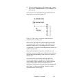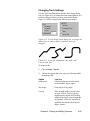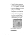
1
CircuitMaker 2000
®
the virtual electronics lab
™
TraxMaker User Manual
professional pcb layout
built-in autorouting
Revision A
Software, documentation and related materials:
Copyright © 1993-2000 Protel International Limited.
All Rights Reserved. Unauthorized duplication of the software, manual or related materials by
any means, mechanical or electronic, including translation into another language, except for brief
excerpts in published reviews, is prohibited without the express written permission of Protel
International Limited.
Unauthorized duplication of this work may also be prohibited by local statute. Violators may be
subject to both criminal and civil penalties, including fines and/or imprisonment.
TraxMaker, CircuitMaker, Protel and Tango are registered trademarks of Protel International
Limited. SimCode, SmartWires and The Virtual Electronics Lab are trademarks of Protel
International Limited.
Microsoft and Microsoft Windows are registered trademarks of Microsoft Corporation. Orcad is
a registered trademark of Cadence Design Systems. PADS is a registered trademark of PADS
Software. All other trademarks are the property of their respective owners.
Printed by Star Printery Pty Ltd
ii
Table of Contents
Chapter 1: Getting Started
Introduction............................................................................................ 1-1
TraxMaker Capabilities .................................................................... 1-1
Differences with Other Applications ..................................................1-2
Getting Ready to Install ..........................................................................1-2
Read the README File ................................................................... 1-2
System Requirements ......................................................................1-3
Installing TraxMaker ............................................................................... 1-3
Installing TraxMaker on a LAN ..........................................................1-3
Technical Support ..................................................................................1-4
About the Documentation ......................................................................1-5
User Manual Contents ......................................................................1-5
Manual Conventions ........................................................................1-7
Using On-line Help ...........................................................................1-7
Chapter 2: Overview of TraxMaker
Introduction............................................................................................ 2-1
Connectivity .....................................................................................2-1
About TraxMaker Layers .................................................................. 2-2
TraxMaker Conventions ................................................................... 2-3
Starting TraxMaker ...........................................................................2-3
The TraxMaker Workspace ................................................................... 2-3
Board Layers ...................................................................................2-4
What is the Current Layer? ...............................................................2-4
Layers: A Closer Look ......................................................................2-5
Using the Mouse .............................................................................. 2-6
Units, Grids & Coordinates .................................................................... 2-6
Changing the Units of Measure ........................................................ 2-6
Snap Grid vs. Visible Grid................................................................2-7
The Coordinate System ................................................................... 2-7
Absolute vs. Relative Origin .............................................................2-8
Finding the Origin ............................................................................2-8
Contents
iii
Finding a Location ...........................................................................2-8
Tool Bar ................................................................................................2-9
Shortcut Keys ........................................................................................2-9
TraxMaker Files .................................................................................. 2-11
Library (.LIB) Files .........................................................................2-12
Autotrax Compatibility ....................................................................2-12
TraxMaker Preferences .......................................................................2-12
Loading a Different Preferences File .............................................2-13
Saving Preferences to a New File ..................................................2-13
Restoring Factory Defaults .............................................................2-13
Basic PCB File Management ..............................................................2-14
Starting, Saving & Closing a PCB File ...........................................2-14
Opening and Reopening a PCB File ..............................................2-14
Reverting to Previously Saved File .................................................2-14
Merging Files.................................................................................2-15
Chapter 3: Tutorials
Tutorial 1: Manual Board Creation .........................................................3-1
Step 1: Getting Started .....................................................................3-2
Step 2: Setting Up the Board Layers ................................................3-2
Step 3: Defining a Board Outline ...................................................... 3-4
Step 4: Placing Components ...........................................................3-6
Step 5: Connecting the Components ................................................3-8
Step 6: Checking Your Work ..........................................................3-13
Tutorial 2: Automated Board Creation ..................................................3-13
Step 1: Creating a Netlist in CircuitMaker .......................................3-14
Step 2: Defining a Keep Out Layer .................................................3-16
Step 3: Loading a Netlist ................................................................3-16
Step 4: Using AutoPlacement .........................................................3-17
Step 5: Using the Auto Router ........................................................3-18
Tutorial 3: Creating New Components .................................................3-19
Step 1: Creating a component from scratch....................................3-20
Step 2: Creating a Component Based on an Existing One .............3-20
iv
Contents
Chapter 4: Placing and Editing Features
The Full Screen Cross Cursor ...............................................................4-1
The Measurement Tool ..........................................................................4-2
The Arrow Tool ......................................................................................4-2
Selecting an Item .............................................................................4-3
Selecting Multiple Items ................................................................... 4-3
Moving Items ...................................................................................4-5
Cut, Copy, Paste, & Delete.................................................................... 4-6
Cutting Items ....................................................................................4-6
Copying Items ..................................................................................4-7
Pasting Items ...................................................................................4-7
Deleting Items ..................................................................................4-7
Refreshing the Screen .....................................................................4-8
Duplicating an Item or Group of Items ...............................................4-8
Panning ........................................................................................... 4-9
The Place Component Tool .................................................................4-10
Editing a Component ..................................................................... 4-11
Finding Components .....................................................................4-13
The Rotate 90 Button...........................................................................4-13
Rotating Items While Moving ..........................................................4-13
Rotating Text ..................................................................................4-14
The Mirror Button .................................................................................4-14
Mirroring Items While Moving .........................................................4-14
The Place Pad Tool .............................................................................4-14
Linear Copy of a Pad .....................................................................4-16
Radial Copy of a Pad ....................................................................4-17
Rotating a Pad...............................................................................4-17
Finding a Pad ................................................................................4-18
Editing a Pad.................................................................................4-18
The Route Pad-to-Pad Without Net Tool ..............................................4-23
The Place Track Tool ...........................................................................4-24
Changing Track Settings ................................................................4-25
Editing a Track...............................................................................4-26
The Break Track Tool...........................................................................4-28
The Re-Route Track Tool .....................................................................4-28
Contents
v
The Place Via Tool ..............................................................................4-29
Editing a Via ..................................................................................4-29
The Place Text Tool .............................................................................4-31
Finding Text ...................................................................................4-32
Editing Text ....................................................................................4-32
Setting Text Size Defaults ..............................................................4-34
The Place Arc Tool ..............................................................................4-35
Editing an Arc ................................................................................4-36
The Place Fill Tool ...............................................................................4-36
Editing Fills ....................................................................................4-37
The Place External Plane Tool .............................................................4-37
Anatomy of an External Plane ........................................................4-37
Changing External Plane Settings ..................................................4-38
Placing an External Plane ..............................................................4-38
Editing External Planes ..................................................................4-39
The Zoom Tool ....................................................................................4-40
The Select Area and Zoom Tool .....................................................4-40
The Fit Board to Window Tool ........................................................4-40
Setting Up the Draw Mode ..................................................................4-41
Chapter 5: Managing Libraries
Managing Component Libraries ............................................................5-1
About Components ..........................................................................5-2
Browsing Component Libraries ....................................................... 5-2
Adding a New Component ...............................................................5-3
Deleting a Component from the Library ............................................5-4
Compacting the Component Library.................................................5-5
Creating a New Component Library .................................................5-5
Opening a Different Component Library ........................................... 5-5
Merging Component Libraries .........................................................5-6
Managing Pad Libraries ........................................................................5-6
About Pads .....................................................................................5-7
Browsing Pad Libraries ................................................................... 5-8
Creating or Editing a Pad ................................................................5-8
Deleting a Pad from the Library .....................................................5-10
Creating a New Pad Library ...........................................................5-10
vi
Contents
Opening a Different Pad Library..................................................... 5-11
Copying Pads from Library to Library ............................................. 5-11
Chapter 6: Nets and Netlists
What is a Net? .................................................................................6-1
What is a Netlist? .............................................................................6-2
TraxMaker Netlist Format .................................................................6-2
Other Netlist Formats .......................................................................6-3
Viewing and Editing Netlists ............................................................6-4
Netlist Limits ....................................................................................6-4
Loading a Netlist ...................................................................................6-5
Making a Netlist ....................................................................................6-8
AutoPlacement .....................................................................................6-9
Before You Run AutoPlacement ....................................................... 6-9
Defining a Keep Out Layer .............................................................6-10
Setting Up Grids and Clearances ................................................... 6-11
Working with Power/Ground Planes ...............................................6-12
AutoPlacement Strategies .............................................................6-14
Using AutoPlacement ..........................................................................6-14
Moving Components to Grid ..........................................................6-15
AutoPlacement Tips .......................................................................6-15
Multiple Libraries with AutoPlacement ............................................6-16
Showing/Hiding Nets .....................................................................6-17
Finding a Net .................................................................................6-18
Identifying a Net .............................................................................6-19
Getting Information About the Board ...............................................6-19
Chapter 7: Routing
Setting Up the Router ............................................................................7-1
Layer Routing Setup ........................................................................7-2
Routing Passes ............................................................................... 7-4
Smoothing .......................................................................................7-9
Variables .......................................................................................7-10
Clearances ....................................................................................7-10
Grid/Clearance Tips .......................................................................7-10
Contents
vii
Using the Autorouter ............................................................................ 7-11
Autorouting the Entire Board ..........................................................7-12
Routing Manually With Net..............................................................7-13
Autorouting Pad-to-Pad Without Net ..............................................7-14
Autorouting a Net ...........................................................................7-14
Autorouting a Net by Name ............................................................7-15
Autorouting a Connection ...............................................................7-15
Unrouting All ...................................................................................7-16
Unrouting a Net ..............................................................................7-16
Unrouting a Connection ..................................................................7-16
Netlists and AutoRouting ................................................................7-16
Getting the Best Result from Autorouting ........................................7-17
Optimizing Netlists .........................................................................7-18
TRAXEDIT.LOG .............................................................................7-20
Design Rules Checking .......................................................................7-20
DRC Error Messages ....................................................................7-22
Chapter 8: Printing and Plotting
Printing PCB Artwork ............................................................................8-1
PostScript Printers ..........................................................................8-1
Photoplotting ...................................................................................8-2
Before You Print a PCB .........................................................................8-2
Setting Up the Printer .......................................................................8-2
Printing the PCB ...................................................................................8-3
Setting Up Print Options .................................................................. 8-4
The Plot Layers ................................................................................8-7
Producing Quality Printouts ..............................................................8-9
Postscript Printing .........................................................................8-10
Chapter 9: Importing and Exporting Files
AutoCAD DXF Files (.DXF) .................................................................. 9-1
Importing DXF files ..........................................................................9-2
Exporting DXF files ..........................................................................9-4
Protel Text PCB Files (.PCB) ................................................................9-6
Pick and Place Report ..........................................................................9-7
Bill of Materials Report ..........................................................................9-8
viii
Contents
Gerber and N/C Drill Files .....................................................................9-9
The Gerber Photoplotting Process .................................................9-10
Creating Gerber Photoplot Files .................................................... 9-11
Naming Gerber Files .....................................................................9-14
Using a Photoplot Bureau ..............................................................9-15
About the Gerber File Format ........................................................9-16
About Aperture Files ......................................................................9-18
Creating Custom Aperture Files .....................................................9-20
Setting Up Aperture Matching ........................................................9-20
Matching Apertures ........................................................................9-21
Numeric Control Drilling ......................................................................9-22
About the .DRL and .TXT Files .......................................................9-23
About Drilling Tools and the .TOL File ............................................. 9-24
Creating N/C Drill Files .................................................................. 9-25
ASCII to Hex Translation ................................................................9-26
Glossary
Index
Contents
ix
x
Contents
CHAPTER 1
Getting Started
Introduction
Welcome to TraxMaker, the most powerful, affordable
printed circuit board layout program available! This proven
layout tool combines professional features with an easy-touse and intuitive interface. And all at a fraction of the cost of
“high-end” software.
Used by itself, TraxMaker offers a complete PCB layout and
autorouting environment with most of the features you’d
find in a program costing thousands more. When combined
with the CircuitMaker® schematic capture and simulation
package, TraxMaker becomes the second half of a tightly
integrated, start-to-finish electronic design system called
CircuitMaker® 2000.
TraxMaker Capabilities
TraxMaker generates through-hole and SMD (surface mount
device) designs of up to six signal layers, plus power and
ground planes, silk screen overlays and solder and paste
masks. Board size can be as large as 32 inches (or 81cm)
square. Placement accuracy is to 1 mil (.001 inch or .025 mm).
A metric/imperial grid system allows you to work accurately
in both measurement systems and the grid can be “toggled”
between metric and imperial modes as you design. The
number of components you can include in your design is
limited only by the memory on your computer.
Full support is included for most popular netlist formats.
Importing a PCB netlist from schematic products allows you
to take full advantage of TraxMaker’s auto component
placement, rip-up and retry autorouting and design rule
checking features. The program will print to Windowscompatible printers and plotters, and outputs Gerber RS274X
files, Excellon™ N/C drill files, Pick and Place files, Bill of
Materials and DXF.
Chapter 1: Getting Started
1-1
Differences with Other Applications
TraxMaker looks and runs like other Windows applications,
and it’s as flexible as you are. However, you should be
aware that TraxMaker is different from other Windows
drawing applications in some fundamental areas.
First, a PCB design is a series of layers, such as the Top and
Bottom signal layers or the silkscreen Overlay layer.
TraxMaker displays and manages these layers independently and some operations, such as track placement, are
layer dependent, that is, you must first select the layer, then
place the track. TraxMaker print/plot options also reflect the
layered design.
Second, PCB design differs from other drawing tasks in its
requirement for extreme precision. As a result, TraxMaker is
more a “placing” environment than a freehand “drawing”
environment. So you may find that some TraxMaker tools
will operate differently from similar tools in other Windows
drawing applications.
Another fundamental difference is connectivity—TraxMaker
has the ability to recognize connections between track
segments, tracks and component pads through netlists
(imported or created internally). TraxMaker also allows you
to retain connections when moving a component, without
breaking its track-to-pad segments. You will be using
connectivity on several levels as you design with
TraxMaker.
Getting Ready to Install
Before installing and using TraxMaker, take a few moments
to read the Software License Agreement at the beginning of
this manual.
Read the README File
Read the README file included with the TraxMaker
program. It has updated information about the current
version of TraxMaker, prepared since this manual went to
press.
1-2
Chapter 1: Getting Started
System Requirements
In order to run TraxMaker properly, you will need:
•
Microsoft® Windows NT4, 95, 98 or 2000
•
PC with Pentium class processor
•
32MB of RAM
•
40MB hard disk space
•
Desktop Area 800 x 600 pixels
•
Color Palette 256 colors minimum
•
CD ROM drive
•
Mouse or compatible pointing device
•
Any Windows-compatible printing device
Installing TraxMaker
To install TraxMaker,
1
Start your Windows operating system.
2
Insert the installation CD into your computer’s drive.
3
From the Taskbar choose Start > Run.
4
Browse to the drive containing the installation disk,
select the Setup file, then choose Open, then choose
OK.
5
Follow the prompts until TraxMaker is installed.
Installing TraxMaker on a LAN
TraxMaker is designed for both single-user and multi-user
operation, so the program can be installed on a LAN for
sharing or exchange files and libraries with other users.
Before installing TraxMaker on a network, you should be
aware that the Software License Agreement (at the front of
the manual) restricts the use of the package to only the
number of users you have purchased licenses for. A singleuser copy, for example, only allows operation of the software
on a single computer at a time.
Chapter 1: Getting Started
1-3
For multi-user operation, each TraxMaker user must be in
possession of his/her own licensed TraxMaker package, or
you must own a Multi-User Site License.
Each network user can have their own library and pad files.
Each user will have a Traxmakr.ini file which will determine
the paths for their library and pad files, their work files, and
all other user-defined preferences.
Technical Support
Protel is dedicated to producing only the finest quality
software and this means supporting the customer after the
purchase. This manual contains detailed information to
answer most questions. Please look it over before contacting
us for technical support. If you encounter other problems
while using TraxMaker or just need general help, contact us
via phone, FAX or Email and we’ll provide prompt and
courteous support.
NOTE: Please be prepared to provide your name and
registration number (found on the back of the User Manual
or on the CD jacket) when contacting us.
Telephone:
801-224-0433
FAX:
801-224-0545
Internet:
http://www.circuitmaker.com
Email:
[email protected]
Future versions of TraxMaker are planned so please feel free
to write and let us know what features or additions you
would like to see. Our goal is to provide a product that will
meet your needs and expectations and feedback from you is
essential if we are to achieve this goal!
1-4
Chapter 1: Getting Started
About the Documentation
TraxMaker comes with two manuals, a User Manual and a
Footprint Library Guide. This User Manual has been
designed to guide you through TraxMaker’s many features
and to simplify the retrieval of specific information once you
have a working knowledge of the product. The Footprint
Library Guide lists all the component footprints in the
TraxMaker libraries, and shows actual size examples of these
footprints.
Professional Edition
Some of the information and features found in the User
Manual are only available with the Professional Edition.
These features will be highlighted by the banner shown at
the left.
The User Manual assumes that you are familiar with the
Windows desktop and its use of icons, menus, windows and
the mouse. It also assumes a basic understanding about how
Windows manages applications (programs and utilities) and
documents (data files) to perform routine tasks such as
starting applications, opening documents and saving your
work.
User Manual Contents
If you are new to Windows, please start with your Windows
system software documentation. TraxMaker is similar in
operation to most other Windows applications. Once you
have mastered a few Windows basics, you’ll be ready to
learn TraxMaker. The TraxMaker User Manual contains the
following sections:
Chapter 1: Getting Started
This chapter gives you a general introduction to the
TraxMaker program. As you read further, you will find
guidelines for installing and configuring TraxMaker.
Chapter 2: Overview
This chapter provides an overview of the TraxMaker design
environment, including many of the tools and features that
you will be using, key concepts and terminology used in
printed circuit board design.
Chapter 1: Getting Started
1-5
Chapter 3: Tutorials
A short “guided tour” of basic TraxMaker design operations; setting up the layers, placing components, connecting
components with tracks, loading a netlist created in CircuitMaker, auto placing components, using the autorouter, and
checking your work.
Chapter 4: Placing and Editing Features
This chapter describes in detail the various placing and
editing tools, most of which are found on the Toolbar and
provide direct access to key TraxMaker design features.
Chapter 5: Managing Libraries
TraxMaker comes with a comprehensive set of libraries of
the most common component footprints, boardblanks and
pads. This chapter shows you how to add new items, list
them, and manage the libraries.
Chapter 6: Nets and Netlists
Information about TraxMaker’s design automation features;
generating and importing circuit netlists, auto component
placement, autorouting and design rule checking.
Chapter 7: Routing
You can route connections on a Board manually, or you can
use any of TraxMaker’s various autorouting options. This
chapter explains all routing options and tells you how to
optimize router settings for best results.
Chapter 8: Printing and Plotting
Complete instructions for using printers and plotters for
generating PCB artwork.
Chapter 9: Importing and Exporting Files
This chapter details TraxMaker’s import and export options,
including the preparation of Gerber format photoplot and
Excellon format Numeric Control drill files.
Glossary
This contains a list of terms used in this manual, and their
definitions.
A comprehensive Index of manual topics follows the
Glossary.
1-6
Chapter 1: Getting Started
Manual Conventions
The following conventions are used to identify information
needed to perform TraxMaker tasks:
Step-by-step instructions for performing an operation are
generally numbered as in the following examples:
1
Choose File > Save.
This means “choose the File menu, then the Save command.”
2
Select the Arrow Tool from the Toolbar.
Menu names, menu commands, and Toolbar options are
displayed in bold type as are text strings to be typed:
3
Notes, Tips, and Warnings
are written here in the margin
for greater visibility.
Type the component name: AXIAL0.5.
The manual also includes some special terminology—words
that are either unique to PCB manufacturing or have some
specific meaning within the TraxMaker design system. Such
terms will be italicized when first introduced. Definitions for
many of these key words will be found in the Glossary, at
the end of the manual.
Using On-line Help
TraxMaker’s on-line Help file (TMHELP.HLP) can be accessed in several ways.
From the Help Menu
To access Help from the Help menu,
1
Choose Help > TraxMaker Help Topics.
2
Choose the Contents tab to see an overview of all Help
topics arranged hierarchically.
OR
Choose the Index tab, then enter a keyword to look up a
specific Help topic.
OR
Choose the Find tab to find Help topics that contain the
word you are looking for.
Chapter 1: Getting Started
1-7
From a Dialog Box
To access context-sensitive Help,
1
Open a dialog box, then press F1 to display Help
specifically tailored for that dialog box.
Double-Clicking the Help file
Even when TraxMaker is not running, you can view the Help
file by double-clicking its icon in the TraxMaker program
group.
1-8
Chapter 1: Getting Started
CHAPTER
2
Overview of TraxMaker
Introduction
Building a TraxMaker PCB design is a straightforward
process of:
•
Defining the physical outline of the PCB.
•
Selecting and placing the required component patterns
from a component library. Or, if working from a schematic netlist, importing and placing (manually or with
the auto placement feature) the components onto the
predefined board.
•
Connecting the component pads with tracks, manually,
with the autorouter, or a combination of manual and
automatic track routing.
•
Checking your work using TraxMaker’s built-in design
rules check tool.
•
Printing, plotting or outputting the required manufacturing artwork or files.
•
Checking Gerber files using a Gerber viewer/editor.
Unlike generic CAD drafting packages, TraxMaker provides
special features that address the unique requirements of PCB
artwork, such as the ability to edit and print or plot the
individual layers that correspond to the manufactured board.
Whether your design is a simple single-sided PCB, or a
multilayer board with power and ground planes, you will be
able to layout every item exactly as it will be assembled.
Connectivity
A key feature of TraxMaker is the way electrical connections
between the elements in your design are recognized.
Chapter 2: Overview of TraxMaker
2-1
This concept of connectivity is the basis of automatic
component placement, autorouting and design rule checking.
The program stores connection information in the form of a
netlist generated by a schematic program or created internally in TraxMaker. TraxMaker accepts netlists directly from
CircuitMaker and imports and exports most other popular
netlist formats, including Protel, Tango, OrCAD PCB II and
others. See Chapter 6: Nets and Netlists for more information.
TraxMaker provides layer support and library component
patterns for both through-hole and surface mount (SMD)
components.
About TraxMaker Layers
TraxMaker stores each design as a series of layers which
correspond, in a general sense, to the layers that make up an
actual printed circuit board. For example, the Top Overlay
layer is used to produce a top layer silkscreen with component outlines and text.
This concept of multilayered design distinguishes TraxMaker from other drawing or design applications. Although
all the layers in your design can be viewed simultaneously,
you will need to select an individual layer in order to place
those items which “belong” to that layer, such as tracks, fills
or text. Figure 2.1 illustrates a basic layout that includes two
layers.
component text
(Top Overlay)
component outline
(Top Overlay)
pad (Multi Layer)
track (Top Layer)
via (Multi Layer)
Figure 2.1. A simple multilayer example.
2-2
Chapter 2: Overview of TraxMaker
track (Bottom Layer)
TraxMaker also includes some special “display layers”
which do not directly correspond to final manufactured
board layers. One example is the Multi Layer. In TraxMaker,
pads and vias can occupy a single layer or be “through
hole,” meaning they can occupy all layers of your PCB. The
Multi Layer allows you to display these items together,
distinct from single layer objects such as tracks.
To simplify editing of your design, TraxMaker allows you to
select the specific layers required for your design and to turn
the display of these layers “on” or “off” as needed.
TraxMaker Conventions
TraxMaker conforms to standard Windows user interface
guidelines. If you are experienced with other Windows
applications, you already know how to start and quit
TraxMaker, save your work, navigate through the file system
to locate and organize your documents and how to make
menu selections using the mouse. If you aren’t familiar with
these basic procedures, see Basic PCB File Management
later in this chapter.
TraxMaker has special features that are not common to other
Windows applications. These options let TraxMaker perform
some of the special tasks unique to PCB design. Most of
these are introduced in this chapter and in Chapter 4:
Placing and Editing Features.
Starting TraxMaker
Once you have installed TraxMaker on your hard disk,
simply launch it from the Taskbar (choose Start > Programs
> TraxMaker 2000 > TraxMaker). You can also create a
short cut for TraxMaker and have the icon display on your
desktop all the time.
The TraxMaker Workspace
When you start TraxMaker the Board window is displayed.
This is where components, tracks, text, fills, and so on are
placed. The maximum board area is 32 x 32 inches (81 cm
square). The TraxMaker workspace also includes the Tool
Bar, Menu Bar, and Status Bar. The Status Bar includes a
special Layer selection list to the left. The Layer selection
Chapter 2: Overview of TraxMaker
2-3
box displays the color assigned to the currently defined
layers. The current filename is displayed above in the Title
Bar.
Board Layers
TraxMaker displays your design as a system of layers that
correspond (with some special exceptions) to the artwork
used to create a PCB. These layers can be displayed or
hidden, as needed. Use the Setup Layers dialog box (choose
Setup > Layers) to display or hide and assign individual
colors to each layer. Figure 2.2 shows the major parts of the
workspace.
Title bar
Tool bar
Menu bar
Board window
Layer selection
Status bar
Figure 2.2. The TraxMaker Workspace
What is the Current Layer?
One layer is always the “current” layer at any given time.
The name and color assigned to this layer is displayed in the
Layer selection box to the left of the Status Bar. Tracks, fills,
external planes, arcs, signal layer pads and text are placed on
a single (the current) layer. You can place components,
2-4
Chapter 2: Overview of TraxMaker
multilayer pads and vias without regard to the current layer
selection; however, selecting, moving, deleting, cutting,
pasting, and copying is layer dependent. Only selecting
with the selection rectangle is layer independent. Once
something is selected, it can be cut, copied, pasted, and
deleted without regard to layer.
Layers: A Closer Look
This section describes each layer in more detail. All layers
are viewed from the top side of the board.
Layer or Plane
Top Layer
Definition
The component side signal (or top
“copper”) layer.
Mid Layers
Any of up to four inner signal layers
(numbered Mid-layer 1, Mid-layer 2,
and so on).
Bottom Layer
Solder side signal layer.
Top Overlay
Top “silkscreen” layer that displays
component shapes/text.
Bottom Overlay
“Silkscreen” for bottom-side components, if any.
Ground Plane
Copper ground plane mid layer
(assigned ground pins connect to this
layer).
Power Plane
Copper power plane mid layer
(assigned power pins connect to this
layer).
Board Layer
A special reference layer, provided for
placement of alignment targets, board
outline tracks or mechanical details.
Board layer details can be printed/
plotted with other layers.
Keep Out Layer
A display only layer which defines the
auto component placement and
autorouter perimeter and “no go”
areas.
Chapter 2: Overview of TraxMaker
2-5
Multi Layer
Displays through-hole pads and vias
which occupy all layers.
While not true layers, the Background and Selections may
have colors assigned to them so you can distinguish
between them.
Using the Mouse
As in other Windows applications, TraxMaker uses the
mouse for clicking, selecting and dragging. When moving
the mouse, a corresponding selection tool (or cursor)
movement occurs on the screen.
Tip: You can return to the
Arrow Tool at any time, by
simply right-clicking with the
mouse.
The familiar “pointer” Arrow Tool is used for standard
Windows operations, such as choosing from menus and
dialog boxes.
You can return to the standard Arrow Tool by selecting the
tool from the Tool bar, pressing Esc, or clicking the right
mouse button.
Units, Grids & Coordinates
Printed circuit boards are usually manufactured to very close
tolerances. TraxMaker provides an absolute design resolution of 1 mil (.001 inch or .0254 mm) which should provide
sufficient precision for most PCB design tasks.
Not all printed circuit boards use the English or “Imperial”
system of measurement. For this reason, TraxMaker also
lets you use the metric system.
Changing the Units of Measure
You can display the Board window, coordinates and other
dimensional information in either millimeters (mm) or mils
(1mil = .001 inch). When you specify a unit of measure, all
measurements and inputs are made in that system.
To change the units of measure,
2-6
1
Choose Options > Setup and click on the Grid/Draw tab.
2
Select either English (mils) or Metric (mm).
Chapter 2: Overview of TraxMaker
Snap Grid vs. Visible Grid
To allow the designer to fully exploit its built-in accuracy,
TraxMaker provides two independent user definable grid
systems: an invisible Snap grid and a Visible grid.
The Snap Grid controls the position of items placed in the
board window. Objects automatically “snap” to the Snap
Grid when they are placed or moved. The Snap Grid also
defines the autorouter grid. By default, this Snap Grid is set
at 25 mils.
The Visible Grid is displayed as a system of small coordinate dots or “tick” marks in the board window background.
This measurement is larger by default, at 1000 mils.
Changing Snap and Visible Grid Values
To change the snap and visible grid values,
1
Choose Options > Setup and click on the Grid/Draw tab.
2
Specify values in the Snap Grid and Visible Grid text
boxes, then choose OK.
Most of TraxMaker’s editing and placement tools take
advantage of the Snap Grid, which allows for very accurate
placement and adjustments.
The Coordinate System
You can find out the cursor position relative to the Board
window origin by looking at the coordinates displayed in the
Status Bar, at the lower left of the Board window (see Figure
2.3). The coordinates measure the distance from the origin in
mils or millimeters depending on the currently selected units
of measure.
Figure 2.3. The default Board window origin is at the
extreme lower left corner, where the cursor is shown.
Chapter 2: Overview of TraxMaker
2-7
Absolute vs. Relative Origin
The absolute origin (default 0,0 coordinate) is the extreme
lower left corner of the workspace (see the cursor position in
Figure 2.3). The relative origin can be placed anywhere in
the workspace.
Setting a Relative Origin
The relative origin lets you temporarily set a new 0,0
coordinate anywhere in the workspace.
To set a relative origin,
1
Choose Options > Setup.
2
Select Relative from the Cursor Mode section.
3
Choose Set Floating Origin, then click on the desired
origin in the Board window.
You can redefine the relative origin at any time.
Finding the Origin
Use the Find Origin feature to quickly move the cursor to the
origin. While this feature can find the absolute origin, it is
particularly useful for locating a relative origin.
To find the origin,
1
Choose Edit > Find > Origin.
Note that the cursor moves to the absolute or relative origin
(depending on what is currently defined).
Finding a Location
Use the Find Location feature (pictured in Figure 2.4) to
quickly move the cursor to a specific location on the Board.
To find a location,
1
Choose Edit > Find > Location.
2
Type the X and Y coordinates in the appropriate text
boxes, then choose OK.
Note that the cursor moves to the location you specified.
2-8
Chapter 2: Overview of TraxMaker
Figure 2.4. Quickly move the cursor to a specific location
using the Find Location dialog box.
Tool Bar
Designing with TraxMaker revolves around four basic
procedures: 1) placing objects in the workspace such as
components, free pads, vias, text strings, tracks, area fills
and arcs; 2) moving objects; 3) deleting objects; and 4)
editing, or changing object attributes such as the width of a
track or the contents of a text string.
You can perform most of these tasks using the buttons on
the Tool bar, which are fully described in Chapter 4.
Shortcut Keys
Command key or “short cut” keys let you select menu
commands and tools directly. The following table lists the
available short cut keys in TraxMaker. Note that command
key shortcuts are not case sensitive.
Keystroke
A
C
E
F
What it Does
Place Arc
Place Component
Place External Plane
Place Fill
Chapter 2: Overview of TraxMaker
2-9
2-10
P
S
T
V
X
Y
Place Pad
Place Text String
Place Track
Place Via
Mirror items in x axis while dragging
Mirror items in y axis while dragging
Alt+A
Alt+D
Alt+Z
Arrow Tool
Delete Tool
Zoom Tool
Ctrl+C
Ctrl+D
Ctrl+F
Ctrl+I
Ctrl+M
Ctrl+N
Ctrl+O
Ctrl+P
Ctrl+S
Ctrl+V
Ctrl+X
Ctrl+Z
Copy
Duplicate
Refresh Screen
Gets Info
Measure
New
Open
Print
Save
Paste
Cut
Undo
F2
Shift+F2
F3
F4
F5
Show All Nets
Hide All Nets
Normal Size/Position
Fit Board to Window
Setup
End
Esc
Page Up
Page Down
Delete
Spacebar
Refresh Screen
Abort current operation
Zoom In on cursor position
Zoom Out on cursor position
Delete
Rotate items while dragging
Chapter 2: Overview of TraxMaker
Note: The arrow keys are
available for "nudging" even
while the mouse button is
being pressed.
+ and - (keypad)
Sequence through all available layers
*
Sequence through routing layers
(keypad)
Arrow Keys
Nudge items using the Left, Right, Up,
or Down Arrow keys during placement or while repositioning. Each
press of an arrow key will move the
selection according to the current
Snap Grid setting.
TraxMaker Files
TraxMaker includes a number of special purpose files in
addition to the TraxMaker application. The following table
lists the various types of files you will use by file extension.
Extension
.APT
How Used
Aperture files
.BOM
Bill of Materials report files
.DRC
Results of a Design Rules Check
.DRL
Excellon format (binary) N/C drill file
.DXF
AutoCAD DXF file
.INI
Preferences file that stores settings
.LIB
Component libraries
.LOG
Results of autorouting a board
.MAT
Text file that records gerber apertures
assignments
.NET
Netlist files
.PAD
Pad libraries
.PCB
Printed Circuit Board files
.PIK
Pick and Place report files
Chapter 2: Overview of TraxMaker
2-11
.SET
File for mapping DXF layers to
TraxMaker layers (when importing
.DXF files)
.TOL
Tool matching file
.TXT
Reference text version of N/C drill file
Library (.LIB) Files
TraxMaker is delivered with a library of standard throughhole and surface mount (SMD or SMT) component patterns
(or footprints). The standard TRAXSTD.LIB library file is
normally loaded automatically whenever TraxMaker is
opened, provided the library is in the folder with the
TraxMaker application. You can create new components and
add them to the standard library or create custom libraries.
However, only one library can be loaded at a time. Each
library can hold a maximum of 600 components. For more
information about libraries, see Chapter 5: Managing
Libraries.
Autotrax Compatibility
All versions of TraxMaker can read and use Autotrax PCB
files, libraries and components without any special conversion.
However, because of program changes, TraxMaker files,
libraries and components are no longer compatible with
Autotrax.
TraxMaker Preferences
TraxMaker stores many user settings, such as printer/plotter
setups, display colors, grid settings and many other options
in a special file called TraxMaker preferences
(TRAXMAKR.INI). This file is updated every time you exit
TraxMaker. You can use different Preference settings or
reload the factory defaults using the Preferences dialog box
pictured in Figure 2.5.
2-12
Chapter 2: Overview of TraxMaker
Figure 2.5. Use the Preferences dialog box to manage
TraxMaker settings.
Loading a Different Preferences File
1
Choose File > Preferences.
2
To load a different Preferences file, choose Load
Preferences, specify the Preferences filename, then
choose Open.
Saving Preferences to a New File
If you need to have a different set of Preferences for each
TraxMaker project, you can create new Preferences files.
1
Choose File > Preferences.
2
Choose Save Preferences, specify a Preferences
filename (use the .INI extension), then choose Save.
Restoring Factory Defaults
If your Preferences settings have become confused, you can
restore them to the way they were when you first started
TraxMaker.
1
Choose File > Preferences.
2
Choose Restore Factory Defaults.
Warning: If you have changed many settings in TraxMaker,
it is recommended that you save these settings to a different
Preferences filename before you restore factory defaults.
Otherwise, you will lose your custom settings.
Chapter 2: Overview of TraxMaker
2-13
Basic PCB File Management
This section explains the basic TraxMaker file management
procedures.
Starting, Saving & Closing a PCB File
The features you will use most often are New, Save, and
Save As.
1
Choose File > New to start a new file.
2
Choose File > Save if you’ve already established a
filename.
OR
Choose File > Save As to give the file a filename. This is
the way to copy a PCB file.
3
Choose File > Close, then Yes to save and exit a PCB
file without exiting TraxMaker.
OR
Choose File > Exit, then Yes to exit TraxMaker and save
your work.
Opening and Reopening a PCB File
Note: The Open command
will open TraxMaker PCB
files, Autotrax PCB and
Protel Text PCB files.
1
Choose File > Open.
2
Select the file with .PCB extension that you want to
open, then choose Open.
You can open any of the last 4 PCB files you’ve had open.
3
Choose File > Reopen.
4
Select the file you want to open.
Reverting to Previously Saved File
If you made changes to a PCB file that you don’t wish to
save, you may “revert” to the last version of the file you
saved under the same filename.
To revert to the previously saved file,
1
2-14
Choose File > Revert.
Chapter 2: Overview of TraxMaker
Merging Files
Merging files lets you combine two or more PCB files
together as one.
To merge a file into the current file,
1
Choose File > Merge.
2
Select the PCB file that you want to combine with the
currently opened file, then choose Open.
You are presented with an outline representing the size of
the Board that is to be merged.
3
Position the outline, then click to complete the merge.
Chapter 2: Overview of TraxMaker
2-15
2-16
Chapter 2: Overview of TraxMaker
CHAPTER
3
Tutorials
The following tutorials provide step-by-step instructions for
basic manual and automated PCB layout in TraxMaker. For a
more thorough explanation of the specific processes used in
these tutorials, see the other chapters in this User Manual.
There are three tutorials, covering the following topics:
Tutorial 1: Manual Board Creation
Tutorial 2: Automated Board Creation
Tutorial 3: Creating New Components (Footprints)
The step-by-step processes covered in the following
tutorials follow the general order in which they would
normally be performed. Working through the examples will
provide a general understanding of the way TraxMaker
works and will illustrate that there is often more than one
way of doing a given task.
Note: The tutorials in this
chapter are based on
TraxMaker's default settings
and default library. If you
have made changes to
either of these, your results
may vary from the illustrated
examples.
Tutorial 1: Manual Board Creation
The first tutorial covers the following topics:
•
Starting a new TraxMaker file
•
Setting up the board layers
•
Defining the board outline
•
Placing components
•
Connecting the components with tracks
•
Checking your work
Chapter 3: Tutorials
3-1
Step 1: Getting Started
Begin by starting the TraxMaker program and, if necessary,
clearing the workspace by choosing File > New.
Most TraxMaker manual PCB layout operations involve one
of four basic tasks: placing objects (such as components,
tracks or pads) onto your Board; moving these objects;
editing objects (for example, changing the track width or pad
shape) or deleting objects.
Step 2: Setting Up the Board Layers
Normally you will start a project by enabling the layers you
will be using in your design.
Before you can access a layer, that layer must be enabled.
Layers must be enabled before they can be displayed or
edited.
For this tutorial, you will need to enable the Board Layer
using the Setup dialog box, as seen in Figure 3.1.
1
Choose Options > Setup, then click on the Layers tab.
2
Enable the Board Layer check box.
Figure 3.1. The Layers tab of the Setup dialog box not only
assigns which layers are enabled, but also lets you control
layer, background, and selection colors.
3-2
Chapter 3: Tutorials
Note that default active layers (such as the Top Layer,
Bottom Layer, Top Overlay, and Multi-Layer) are enabled.
The Board Layer is a reference layer that serves as a “master
page” for your design. On it you can place trim marks or text,
indicate mounting holes or other mechanical details or any
element that you will want reproduced along with selected
layers in the finished artwork. The Keep Out layer is another
reference layer, used to define auto component placement
and autorouter perimeter and “no-go” areas.
The Layers tab of the Setup dialog box also lets you assign a
unique color to each layer.
To assign a new color or pattern to the board layer,
1
Click the Board Layer color box (to the right of each
layer designation).
2
Select a new color from the dialog box pictured in Figure
3.2, then choose OK.
OR
Choose Define Custom Colors, select a color from the
palette or define it by specifying Hue, Sat, Lum, Red,
Green, and Blue values. Then choose Add to Custom
Colors to include it on the main color palette.
Figure 3.2. Using the Colors dialog box, you can assign
different colors to layers, or create new colors to assign.
Chapter 3: Tutorials
3-3
As you proceed with this tutorial remember that although
several layers can be “active” and displayed simultaneously,
only one layer is the current layer. Single layer items such as
tracks, fills, arcs or text are always placed on the “current”
layer. The current layer name and color is displayed at the
bottom of your screen, in the Layer Selection box to the left
of the Status Bar.
Step 3: Defining a Board Outline
Tracks (or traces) are placed to connect component pads or
free pads on the signal layers (Top Layer, Mid Layers,
Bottom Layer).
However, tracks can also be placed as nonelectrical lines on
the Top or Bottom Overlay, Board Layer and Keep Out
Layer.
For example, tracks are used to define the board outline (the
boundary of the working area). To do this,
Hint: Status Bar messages
provide valuable information
whenever you select a tool
from the Tool Bar or perform
other actions.
3-4
Chapter 3: Tutorials
1
Click the Layer selection list box at the bottom of your
screen, left of the Status Bar.
2
Select the Board Layer (the one that you activated
previously).
3
Select the Place Track tool from the Tool Bar.
Notice the message on the Status Bar: “Click to place
track, right click to exit placement.”
4
Move the cursor close to the lower left corner of the
workspace (0,0 coordinate). This is called the origin of
the Board window.
5
Now carefully position the cursor at X 100, Y 100 mils
and click once.
6
Move the cursor to the X 3100, Y 100 mils position,
and click once.
7
Move the cursor to the X 3100, Y 3100 mils position,
and click once.
8
Move the cursor to the X 100, Y 3100 mils position,
and click once.
9
Now move the cursor to where you began, the X 100, Y
100 mils position, click once, then right-click.
The result of your track placement should look like Figure
3.3.
Figure 3.3. By following the previous steps, you can create
this board outline, which is 3000 by 3000 mils or 3 inches
square.
You have probably noticed by now that track placement in
TraxMaker is different than other Windows drawing applications, which let you draw a line using a simple “click-anddrag” technique. TraxMaker, on the other hand, lets you
precisely mark the starting point, segment breaks and end
points of tracks, providing the precise placement control
required for accurate PCB layout.
Chapter 3: Tutorials
3-5
Step 4: Placing Components
Although each component is stored as a single entity, it is
actually a collection (or “group”) of standard TraxMaker
primitives (tracks, pads, arcs, and text). These component
primitives belong to various layers as described below.
Regardless of the current layer, components are placed on
either the top or bottom side of the PCB.
A component includes an outline (tracks and/or arcs on the
Top or Bottom overlay) to indicate physical shape of the
component. The DIP package component shown in Figure
3.4 contains Multi layer pads.
Designation
Label-Value
Figure 3.4. Component text, which is added during
placement and displayed on either the Top or Bottom
Overlay, includes a Label-Value (DAC0800), and a
Designation (U7).
Creating new components is simply a matter of placing and
grouping primitives, which can then be added to the current
library. You can also create new components based on
existing ones. See Tutorial 3 and Chapter 6: Managing
Libraries for more information on creating custom components.
Component outlines are displayed on the Top or Bottom
overlay (or silkscreen) layer. Component text (designator or
label-value) can be assigned to either the overlay or “copper” layers. Top and Bottom overlay layers are printed onto
the Board surface as an aid to locating components during
and after assembly.
1
3-6
Chapter 3: Tutorials
Click the Place Component tool on the Tool Bar or press
the C shortcut key on the keyboard.
2
Scroll through the Components list box, pictured in
Figure 3.5, until you find the DIP16 package, then select
it.
Figure 3.5 . Use the Component Selection dialog box to
choose and place a component.
3
Click Place.
4
Type U1 in the Designator text box in the dialog shown
in Figure 3.6. Leave the Label-Value text box empty.
Choose OK.
Figure 3.6. For this tutorial, type U1 as the component’s
Designation.
Tip: If you make the snap
grid too small, it becomes
difficult to precisely place
or align items.
5
Press the Spacebar once to rotate the component 90
degrees counterclockwise.
6
Drag the component to X 400 Y 2300, then click once to
place it.
The component will be redrawn using the Top Overlay
Chapter 3: Tutorials
3-7
layer color to display the outline and designation of the
component and the Multi layer color to display the
pads.
7
Repeat steps 1 through 4, except type U2 as the second
component’s designation. Choose OK.
8
Drag the component to X 1400 Y 2000, then click once
to place it.
9
Now select and place an AXIAL0.3. Designate this
component as R1. Place “R1” at X 550 Y 1700.
If you have followed the previous steps carefully, your
components should be laid out like the illustration in Figure
3.7. If not, you can drag the components to recreate the
approximate layout indicated. Remember, as you drag, you
can press Spacebar, x or y to change the component
orientation.
Figure 3.7. This is the way your component layout should
look after completing the steps thus far in the tutorial.
Step 5: Connecting the Components
Tracks (also called traces) may be routed on the Top layer,
any of four Mid layers or on the Bottom layer (also called
the solder side). Vias are placed at the point where tracks
pass from one layer to another.
3-8
Chapter 3: Tutorials
Selecting a New Track Size
When you placed tracks on the Board layer to define the
outline of the PCB you used tracks which had the (default)
width of 12 mils. However, for this example you will select a
larger size of 15 mils.
To change the default track size,
1
Choose Options > Setup. The Track setup options are
located in the upper left corner under the General tab
(see figure 3.8.)
2
Type 15 in the Default Width text box, then choose OK.
Figure 3.8. The Track and Via setup options are found
under the General tab of the Setup dialog box.
Selecting the Via Size
A via is a special type of pad used to pass current from one
layer of a PCB to another. Like through hole pads, TraxMaker vias occupy the Multi Layer. Another setting you’ll
change is the via size (see Figure 3.8.) A larger via size will
work better with the larger track size you just chose.
To change the default via size,
1
Choose Options > Setup. The Via setup options are
located on the left side under the General tab (see Figure
3.8.)
2
Type 60 in the Via Size text box, then choose OK.
Chapter 3: Tutorials
3-9
Identifying Components and Pins
Before you can route your connections, you will need to
identify the components and pin numbers to be connected.
The Find option lets you quickly move the cursor to a
predetermined location. This can save you from having to
constantly zoom in to see the pin numbers and zoom out to
navigate around your design and is particularly useful for
large or complex layouts.
To quickly find components and pin numbers,
1
Choose Edit > Find > Component.
2
Select U1 from the Component list box and 1 from the
Pin list box. Choose OK.
Note that the cursor goes to component U1, pin number 1,
and that the component is selected.
Placing Tracks
Now that you have set up the track and via sizes, and you
know how to find components and pins, you’re ready to
make your first connection. Your objective is to connect U11 to U2-1 by first placing a via. Make sure that you are on
the Top Layer, then follow these steps:
Tip: It’s easier to
place items precisely
when you Zoom in on
the area where you
are working.
Tip: You can toggle
between layers using
the *, + or - keys on
the keypad. When you
toggle between copper
layers while placing a
track, a via is placed
automatically.
3-10
Chapter 3: Tutorials
1
Select the Place Via Tool on the Tool Bar.
2
Position the cursor at X 400 Y 2000, then click to place a
via there. Right-click to turn off the Place Via Tool.
3
Select the Place Track Tool from the Tool Bar.
4
Click once at the center of U1-1.
5
Drag the track to the via you placed earlier. Position the
cursor on the center of the via then click again. Rightclick to turn off the Place Track Tool.
6
From the Layer selection list box on the Status Bar,
select Bottom Layer.
7
Select the Place Track Tool again and click once at the
center of U2-1.
8
Drag a track to the same via as before and connect the
track appropriately.
9
To see an accurate picture of the changes you’ve made,
choose View > Refresh Screen or press the End key on
the keyboard.
Now you have two components that are connected by two
tracks and a via, as shown in Figure 3.9.
Figure 3.9. This is how your Board should look after
completing the preceding steps.
In most cases, the track will snap to the grid position that
corresponds to the center of the pad or via (when you are
manually laying tracks). If you change the grid or select a
very fine grid, it is possible to miss the pad center and fail to
establish connectivity.
Keep grids standardized, if possible, and make sure you
manually lead tracks to pad centers. Otherwise the track may
appear connected (depending on the zoom level) when it is
actually isn’t.
As you moved the cursor during track placement, the
selected track segments “snapped” to either horizontal,
vertical and 45 degree segments. This is called orthogonal
track placement and is considered standard practice,
particularly if the board is to be pen plotted or photoplotted.
See Chapter 4: Placing and Editing Features for more
information about Track settings.
Chapter 3: Tutorials
3-11
Using the Pad-to-Pad Router
One of the tools included on the Tool Bar is the Route Padto-Pad Without Net Tool. This tool uses the Router settings
to automatically route a track between two pads (see
Chapter 7: Routing for more information). These settings
define the grid, track and via sizes used when routing and
the clearances the router will maintain as it makes connections. For this tutorial, you will use the default settings.
To connect components using the Route Pad-to-Pad
Without Net tool,
1
Select the Route Pad-to-Pad Without Net tool on the
Tool Bar.
2
Move the cursor to R1-2, click and hold the mouse
button. Pin 2 of R1 will be highlighted when you place
the tool over it.
3
Drag the cursor to the destination pad U2-1 and release
the mouse. TraxMaker connects the two pads, placing
vias as needed.
4
For practice, complete the following connections: U1-12
to U2-9 and U1-13 to U2-6. Your “routed” PCB should
now look similar to Figure 3.10.
Figure 3.10. The tutorial Board, after using the Route Padto-Pad Without Net tool.
3-12
Chapter 3: Tutorials
Step 6: Checking Your Work
Once your PCB has been laid out and routed, TraxMaker
provides additional features for design verification.
1
Choose Help > Get Info.
2
Read the information in the dialog box pictured in Figure
3.11, choose the buttons to get more detailed information, then choose OK.
Figure 3.11. Find out information about your Board using
the Get Info feature.
If you have worked through the steps in this tutorial, you
have had a good overview of basic TraxMaker operations.
Whether you are placing, selecting , moving, deleting or
editing, the process is much the same.
Tutorial 2: Automated Board
Creation
While you can design everything manually, TraxMaker has
many features that automate the process of designing
printed circuit boards. TraxMaker is compatible with most
Chapter 3: Tutorials
3-13
standard schematic entry programs, and it is tightly integrated with the CircuitMaker® schematic capture and
simulation program. This tight integration between CircuitMaker and TraxMaker makes it possible to go from schematic to PCB by simply clicking a few buttons.
This second tutorial covers the following topics:
•
Creating a netlist in CircuitMaker and automatically
moving to the board layout using the TraxMaker
button.
•
Importing netlists from other schematic programs and
manually:
Defining a Keep Out Layer
Loading the netlist
Using AutoPlacement
•
Using the Autorouter
If you are importing a TraxMaker netlist from CircuitMaker,
begin here with Step 1, then skip over to Step 5. If you are
loading a netlist that is in a format other than TraxMaker
format, or you are loading a netlist without using CircuitMaker, begin with Step 2 and continue sequentially through
the tutorial.
Note: CircuitMaker® is a
companion product to
TraxMaker, for schematic
capture and simulation.
Step 1: Creating a Netlist in CircuitMaker
This step will show you how to convert a CircuitMaker
schematic drawing into a netlist—a series of connected
pads, vias, components, and tracks—and then automatically
move to the board layout using the TraxMaker Button.
1
Start CircuitMaker.
2
Open PCB.CKT. This is a simple voltage regulator
circuit. The Signal Generator and external load are
placed in the circuit for simulation purposes only and
will not be included in the netlist for board layout.
Each device in the circuit has been assigned a LabelValue, Designation, Package and Pin Numbers. These
are required in order to create a netlist. The name in the
Package field of each CircuitMaker part must match one
3-14
Chapter 3: Tutorials
of the component names available in TraxMaker. For
example, if you have a 7400 chip in your schematic, the
Package name for that device should be DIP14 so that
TraxMaker can choose and place the correct component
pattern for that device. See the Footprint Library Guide
for a complete listing of all TraxMaker component
patterns.
3
Click the TraxMaker button in the CircuitMaker toolbar.
When you are exporting a TraxMaker PCB netlist from
CircuitMaker, you can choose to automatically start
TraxMaker, load the netlist, create a keep out layer and
Auto Place the components.
TraxMaker Button
After you’ve clicked the TraxMaker button, the
following CircuitMaker dialog box appears:
Figure 3.12. CircuitMaker’s Export PCB Netlist Dialog
Box. From here you can choose what netlist format you
which to export, and use the automated TraxMaker features
listed.
4
Change the Board Size fields to X 2000 and Y 1000,
then click OK.
5
CircuitMaker will prompt you to save the TraxMaker
netlist, using the circuit’s filename with a .net extension.
Click Save.
6
TraxMaker then opens automatically, a Keep Out layer is
drawn, the netlist loads and a Netlist Load report opens
to show the results of the loaded netlist. Click OK, and
the components are then spread out on the board.
You are now ready to proceed with the routing, so move
ahead directly to Step 5: Using the Autorouter.
Chapter 3: Tutorials
3-15
Step 2: Defining a Keep Out Layer
If you are loading a netlist that is in a format other than
TraxMaker format, or you are loading a netlist without using
CircuitMaker, proceed now with Steps 2 through 5.
One of the most important layers for automated board
creation is the Keep Out layer. Its purpose is to define “keep
out” areas so that the AutoPlacement and Auto Router
features know where to place components and how to route
them. Placing a rectangle of tracks on this layer creates a
perimeter which is never crossed nor touched.
To define a Keep Out boundary,
1
Start TraxMaker and choose File > New to start a new
PCB file.
2
Choose Options > Setup, click on the Layers tab, then
select Keep Out Layer to activate it and choose OK.
3
Click on the Layer selection list at the bottom of your
screen, then select the Keep Out Layer.
4
Select the Place Track tool on the Tool Bar.
5
Place the cursor at X 100 Y 100 and click once.
6
Move the cursor to X 100 Y 1100 and click.
7
Move the cursor to X 2100 Y 1100 and click.
8
Move the cursor to X 2100 Y 100 and click.
9
Finally, move the cursor to where you started (X 100 Y
100), click once, then Right-click to turn off the Place
Tracks tool.
You now have a 2" x 1" rectangular Keep Out boundary.
Step 3: Loading a Netlist
A netlist is a text file listing all the components and connections for an electronic circuit. Netlists allow automated
component placement, automated routing of connections,
and design rule checking. These functions eliminate much
of the tedious manual effort inherent in PCB design.
Your next objective is to load a netlist (this example uses
Pcb.net created in CircuitMaker, which is included with your
copy of TraxMaker).
3-16
Chapter 3: Tutorials
1
Choose Netlist > Load Netlist, and select the type of
netlist you wish to import (in this case, TraxMaker).
2
Select Netlist and Components, then choose OK.
3
Select the netlist file you wish to import (Pcb.net for this
example), then choose Open.
4
You are prompted to click at the location where you
want to place components. Click somewhere inside the
Keep Out area. Notice that the components of the netlist
are piled on top of one another in one place on the
Board. This is normal, as they will be arranged later
using the AutoPlacement feature.
5
Examine the information in the Netlist Load dialog box.
For this tutorial, you’ll accept the default options.
Choose OK.
For more information about netlist options, see Chapter 6:
Nets and Netlists.
Step 4: Using AutoPlacement
AutoPlacement relieves you from having to individually
select components from the library and place them one at a
time in the Board window. AutoPlacement also groups
components using placement strategies to make final
optimization of the layout more efficient. Read more about
AutoPlacement settings and options in Chapter 6: Nets and
Netlists.
The next step is to use AutoPlacement to spread the
components contained in the Netlist you just loaded.
1
Choose Netlist > AutoPlacement > Arrange Components.
Using the autorouter’s Grid settings (specified under the
Grid/Draw tab of the Setup dialog box), AutoPlacement
places the components as best as it can within the Keep Out
layer. For more information about see Setting Up Grids and
Clearances in Chapter 6: Nets and Netlists.
While you could move components to more desirable
locations within the Keep Out Layer, this tutorial assumes
that you will leave the components the way they are spread
using the AutoPlacement. Moving components may produce
different results than what is illustrated in this tutorial.
Chapter 3: Tutorials
3-17
Displaying the “Ratsnest”
Ratsnest usually refers to all the netlist connections
between the components on the board (see Figure 3.13). It
is a picture of the literal connections between components
without any routing.
To show the ratsnest,
1
Choose Netlist > Show Nets > All Nets.
Figure 3.13. This seemingly tangled mess of connections is
called a “ratsnest”—the literal connections before routing.
Step 5: Using the Auto Router
TraxMaker uses a grid-based rip-up-and-retry multi-pass
autorouter, optimized to achieve a high rate of completion at
reasonable costs (for example, via count and total connection distance). The autorouter is extremely flexible, with
many options allowing the user to configure the router for a
variety of design types. You can route an entire board (as
you will in this tutorial), or an individual net or a single
connection. For more information about the autorouter
settings and options, see Chapter 7: Routing.
Your next task is to route the components that you have
placed on the board.
1
Choose Route > Board.
2
Deselect Save Log file, type the full filename of the
netlist in the Netlist Filename text box (Pcb.net), then
choose OK.
While the log file is an important way of checking
autorouting performance, you’ll turn it off for this tutorial.
3-18
Chapter 3: Tutorials
The Status Bar displays information about the router’s
progress. When the router finishes, TraxMaker displays a
connected board, similar to the one pictured in Figure 3.14.
Figure 3.14. When routing a board, results may vary
depending on your settings. This shows how the routing
might look for the example used in this tutorial.
What if the Router Doesn’t Complete 100%?
It’s possible that after you have autorouted a board, the
Router will not have completed all the connections. For
optimization techniques, see Chapter 7: Routing.
For information about outputting your routed PCB, see
Chapters 8 and 9.
Tutorial 3: Creating New
Components
The third tutorial covers the following topics:
•
Creating a new component from scratch.
•
Creating a new component based on an existing one.
You can create components in one of two ways. The first
way is to create individual primitives, group them, then add
them to the library. The other way is to base a new component on an existing one. Both of these methods are described below (this same information can also be found in
Chapter 5: Managing Libraries).
Chapter 3: Tutorials
3-19
Step 1: Creating a component from
scratch
1
Using the tools on the Tool Bar (Place Track, Place
Pad, Place Arc, etc.) create the component as you
would like it to appear. You can use the Duplicate
command from the Edit menu to quickly place rows or
columns of evenly-spaced pads.
Caution: Regardless of how it will be used, draw the
new component as though it were going to be mounted
on the top layer, using through-hole or top layer pads
and top overlay.
Note: Pin 1 of a component
is the reference point,
meaning the rotation axis
and the placement cursor will
be based on the position of
that pin.
2
Give each pad in the new component a pad designation
(pin number). See the Editing a Pad section of Chapter
4: Placing and Editing Features for more details on
pad designations.
3
Choose the Arrow Tool and select all the primitives of
the new component by dragging a selection rectangle
around them.
4
Click the Place Component tool on the Tool Bar.
5
Choose Add, type a package name for the new component, then choose OK.
6
Choose OK to confirm the addition.
7
To view the new component, select the component
name from the list.
Step 2: Creating a Component Based on
an Existing One
Suppose you need a component that is similar to one
already in your library. Instead of creating an entirely new
component from scratch, you can ungroup the existing
component into its primitives then edit the parts. Then you
can save the edited version as a new library component.
This method is also useful if you want to make minor
adjustments to existing library patterns.
3-20
Chapter 3: Tutorials
To base a new component on one that already exists,
1
Select a component that has been placed on the Board.
OR
Click the Place Component tool on the Tool Bar, select a
component, choose Place, place the component
somewhere on the Board, then select it.
2
Choose Edit > Ungroup Component.
3
Choose OK to confirm the ungrouping.
Even though the component appears unaltered (except that
component text has been removed), each element of the
component is now in its primitive state. This means that
instead of a single component, it is now a collection of
tracks, arcs, and pads.
4
Use the tools on the Tool Bar to delete, edit, or add
elements to the component.
5
Select the Arrow Tool from the Tool Bar.
6
Select (group) all the elements of the edited component
by dragging a selection rectangle around them.
7
Select the Place Component tool on the Tool Bar.
8
Choose Add, type a package name for the new component, or use the old name to replace the existing
component with this new one. Choose OK.
9
Choose OK to confirm the addition.
10 To view the new component, select the component
name from the list.
Chapter 3: Tutorials
3-21
3-22
Chapter 3: Tutorials
CHAPTER
4
Placing and Editing Features
Most of TraxMaker’s drawing, placing and editing features
are accessed through the Tool Bar, displayed at the top of
the Board Window. To select a tool, simply click its icon on
the Tool Bar. You can turn off a tool by clicking the right
mouse button or by selecting another tool. In this chapter,
the corresponding Tool Bar icon is shown next to each
editing feature that originates from the Tool Bar.
The Full Screen Cross Cursor
TraxMaker lets you choose between a standard or full screen
cross cursor. The crosshairs of the full screen cross cursor
extend across the entire board, for increased accuracy. This
option is very useful for precisely placing and aligning items
with other parts of the board.
To select the full screen cross cursor,
1
Choose Options > Setup.
2
Enable the Full Screen Cross Cursor check box found
in the Cursor Mode section of the General tab, then click
OK.
Note that the cross cursor (standard or full screen) is only
active when you are placing or moving design objects.
Figure 4.1. The full screen cross cursor extends across the
entire screen, for accurate placement.
Chapter 4: Placing and Editing Features
4-1
The Measurement Tool
Tip: To ensure a precise
start and end point for
measurement, zoom in
on the area you are
measuring.
The built-in point-to-point measurement tool allows you to
precisely measure distances between design objects on your
board, eliminating the need to manually calculate distances
using the coordinates. When measuring between pads, each
pad is highlighted as you move the cursor over the pad.
Hold down the Alt key when you click on a pad to snap to
the center of the pad.
To use the measurement tool,
1
Choose Edit > Measure.
2
Click once on the starting point you wish to measure
from.
3
Click again on the ending point you wish to measure to.
A Measurement dialog box appears, showing the
distance measured, the X distance, and the Y distance
between the two points.
4
Click OK and then measure the next two points. Repeat
steps 2 and 3 for as many measurements as you wish to
make.
5
Right-Click or choose another editing tool to end the
Measurement option.
The Arrow Tool
Use the Arrow Tool to select, move and edit items. You can
double-click (click twice with the mouse in rapid succession)
with the Arrow Tool on most items to edit their specific
properties. Selected items can be moved, deleted, cut,
copied, duplicated, rotated or mirrored.
4-2 Chapter 4: Placing and Editing Features
Selecting an Item
Multilayer components can be selected from any layer. If the
component is a surface mount device (SMD), you must be
on the correct layer.
To select an item,
1
Click the Arrow Tool on the Tool Bar.
2
Position the point of the arrow over the item on your
board.
3
Click the left mouse button once.
You know that an item is selected if it changes color. White
is the default selection color. See Chapter 3: Tutorials to
learn how to change the colors of your board’s layers and
selections.
Selecting Multiple Items
Multiple items can be selected using the Arrow Tool or by
choosing from the various global Select options from the
Edit menu.
To select multiple items using the Arrow Tool,
1
Click the Arrow Tool on the Tool Bar.
2
Drag a box around the group of items you want to
select. Items are selected on all layers of the board.
OR
Hold down the Shift key and click on each item. Only
items on the current layer or multi-layer items can be
selected.
Now you may cut, copy, duplicate, delete, drag, rotate or
mirror the selection items.
Selecting Connections and Nets
Holding the Ctrl or Alt keys while you click with the Arrow
Tool allows you to select connections or entire nets.
Chapter 4: Placing and Editing Features
4-3
Press
Ctrl+Click
To Select
All track segments and vias that form
the single connection between two or
more pads.
Alt+Click
An entire net (or series) of connected
tracks, pads, and vias.
Ctrl+Shift+Click
Multiple connections, one per click.
Alt+Shift+Click
Multiple nets, one per click.
Once selected, you may edit, cut, copy, duplicate, delete,
drag, rotate or mirror the selection items.
Global Select Options
Along with the Arrow Tool select options, there are also
many global select options available from the Edit menu.
To globally select items,
1
Choose Edit > Select.
2
Click one of the following select options
Option
All
To Select
Everything on the entire board.
All on Layer
Everything on a single board layer.
All Tracks
All tracks on the entire board.
All Free Pads
All free pads on the entire board.
All Vias
All vias on the entire board.
All Text Strings
All text strings on the entire board.
All Components
All components on the entire board.
Now you may cut, copy, duplicate, delete, drag, rotate or
mirror the selection items.
Including Different Layers in a Selection
You can specify the layers that are included in an area
selection before you cut, copy, delete, or move a group of
items on the Board.
4-4 Chapter 4: Placing and Editing Features
To include different layers in a selection,
1
Choose Options > Setup and click on the Layers tab.
2
Select one of the following options from the Cut, Copy,
Delete, Move group box, then choose OK.
Option
All Layers
What it Does
Includes all layers in the selection
without confirmation.
Current Layer
Includes only the currently selected
layer, as displayed in the Layer
Selection text box on the Status Bar.
Ask Layers
Prompts you whether you want to
perform an action on all layers. If you
choose No, only the currently
selected layer is affected.
Moving Items
Note: You can abort a
move by pressing the
Esc key before releasing
the mouse button.
1
Select the Arrow Tool from the Tool Bar.
2
Position the cursor over the item you want to move,
then click and hold the mouse button.
OR
Select a group of items as described above, position the
cursor over the group of items, then click and hold the
mouse button.
3
Drag the item(s) to a different location, then release the
button.
Components, pads, text strings and groups of items can be
rotated or mirrored while they are being dragged. Press the
Space bar to rotate, the X key to mirror in the x direction or
the Y key to mirror in the y direction. The center of rotation/
mirroring will be at the cursor position. The layers contained
in the selection that are actually moved depend on the
setting you have made in the Setup Layers dialog box. To
undo a move choose Edit > Undo Move.
Chapter 4: Placing and Editing Features
4-5
Figure 4.2. When you drag a selected component, the
tracks connected to that component can also drag.
Dragging Tracks
The C9 component in the Figure 4.2 has been dragged to a
new location. Notice in this case that the component’s
connected tracks drag with the component and remain
connected. You can specify whether or not connected tracks
drag with the item. See Changing Track Settings later in
this chapter for more information.
Cut, Copy, Paste, & Delete
Use Cut, Copy, Paste and Delete after you have selected
items on the Board. Duplicate (found on the Edit menu)
places a number of copies (that you specify) of any selected
items.
Cutting Items
Cut removes the selection from the Board window and adds
it to the Clipboard.
To cut an item,
1
Select an item or group of items, then click the Cut
button on the Tool Bar. The mouse cursor will be
changed to a crosshair.
2
Click on a reference point of the item being cut. This
reference will be used when the item is pasted.
To undo a cut, choose Edit > Undo Delete.
4-6 Chapter 4: Placing and Editing Features
Copying Items
Copy duplicates the selection onto the Clipboard.
To copy an item,
1
Select an item or group of items, then click the Copy
button on the Tool Bar. The mouse cursor will be
changed to a crosshair.
2
Click on a reference point of the item being copied. This
reference will be used when the item is pasted.
Pasting Items
Paste copies the selection in the Clipboard back to the Board
window.
To paste an item,
1
Click the Paste button on the Tool Bar.
2
Drag the item into position and click with the left mouse
button to place the item.
If nothing is on the Clipboard, the Paste button will be
unavailable. You can abort a paste by pressing the Esc key
before clicking the mouse button. To undo a paste, immediately press the Delete key on the keyboard while the items
are still selected.
Deleting Items
Use the Delete Tool or press the Delete key to remove items
from the board.
To delete an item using the Delete Tool,
1
Make sure the layer containing the item you want to
delete is active.
2
Select the Delete Tool on the Tool Bar.
3
Position the lightning bolt over the item you want to
delete, then click.
Chapter 4: Placing and Editing Features
4-7
To delete items using the Delete key,
1
Select the items you want to delete, using the selection
options described previously.
2
Press the Delete key on the keyboard.
To undo a delete, choose Edit > Undo Delete.
Refreshing the Screen
Sometimes after you move or delete items, the board will
look fragmented. To restore an accurate picture of the board,
choose Edit > Refresh Screen or press the End key on the
keyboard.
Duplicating an Item or Group of Items
Duplicate is similar to the Copy and Paste tools but adds
additional features to automate repetitive placement. This is
useful if you want to place an array of pads, for example (see
Figure 4.3) or to panelize a final layout into multiple copies of
a board for production.
To duplicate an item or group of items,
1
Choose the Arrow Tool from the Tool Bar.
2
Select an item or group of items.
3
Choose Edit > Duplicate.
4
Specify how many times you want to duplicate the item
and where you want to place the duplicated item (see
the following option table), then choose OK.
Note: See also Linear Copy
of a Pad and Radial Copy of
a Pad later in this chapter.
Figure 4.3. Duplicate lets you repeat an item several times
with a defined spacing, like this series of pads.
4-8 Chapter 4: Placing and Editing Features
Option
Count
Lets You
Set the number of duplicates up to a
maximum of 1000.
X and Y offset
Specify the positioning of each
duplicate along either axis. For
example, an X offset setting of 100
and Y offset setting of 0 will duplicate the selected item(s) in 100 mil
increments to the right the number of
times specified in the Count text box.
Duplicate All Layers
Choose whether or not to duplicate
all the layers in the selection. If you
want to duplicate only the selection
on the currently selected layer, then
deselect this option.
Use Same Designators Choose whether or not to use the
same component designations in the
duplicates as in the original. This
should be enabled when panelizing a
final layout for production.
Panning
Panning is the ability to move the viewing area of the screen
as you work on a magnified area of the Board window.
TraxMaker provides automatic panning when placing or
moving selected items.
To pan,
1
Select one of the placement tools on the Tool Bar, such
as Place Component or Place Pad, or select the Arrow
Tool to select a large area of the board.
2
Use the tool as you would normally and try sliding the
tool off of the board window. Notice that the viewing
area shifts as you move the tool.
Chapter 4: Placing and Editing Features
4-9
The Place Component Tool
This tool lets you select from among a library of components
(see Figure 4.4), add text labels to the component, then place
it on the board. See Chapter 5: Managing Libraries for
more information about defining new components and
working with different libraries.
To place a component,
1
Click the Place Component Tool on the Tool Bar.
2
Scroll through the Components list box until you find
the component you want to place.
3
Select the component package name, then click Place to
put the component on the board. You can also click
Place and Return to place the component and automatically return to this dialog box to select another component.
4
Type a label or value (to appear on the board with the
component) in the Label-Value text box. A component
label or value is the component’s electrical value, such
as .01uF, 470k or 1N4002.
5
Type a designation for the component in the Designation text box. A component designation usually consists
of a letter such as U, C, J, or R followed by a number.
You may decide to call an edge connector J3 or a
capacitor C4.
6
Choose OK, and while placing, press the Spacebar to
rotate the component outline counterclockwise in
increments of 90 degrees until it is in the desired
position or press X or Y to mirror the component on its x
or y axis.
7
The reference point for the component is pin 1. Move
the component to the location where you want to place
it, then click once.
4-10 Chapter 4: Placing and Editing Features
Figure 4.4. The Component Selection dialog box lets you
select a component from a list, then place it on the board.
Editing a Component
You can easily edit a component in TraxMaker. Edit options
allow you to rename a component Package, change the
Label-Value, Designation, display or hide component text
and make other changes.
To edit a component,
1
Select the Arrow Tool from the Tool Bar.
2
Double-click on the component that you want to change
(don’t click on a pad).
3
From the Edit Component dialog box (see Figure 4.4),
make the desired changes, then choose OK.
Figure 4.5. The Edit Component dialog box lets you
change the characteristics of a component.
Chapter 4: Placing and Editing Features
4-11
Option
Package
Lets You
Change the component’s Package
name. Renaming a component will
not change the pattern or affect the
library.
Label-Value
Change the component’s Label-Value.
For example, change a capacitor’s
value from 0.1uF to 0.3uF.
Designation
Change the component’s Designation. For example, change a resistor’s
name from R34 to R43.
Height
Change the height of the tracks used
to draw Label-Value and Designation
text.
Line Width
Change the thickness of the tracks
used to draw Label-Value and
Designation text.
Visible
Specify whether the component’s
Label-Value and Designation text
appear with the component.
Top or Bottom
Specify whether the component is
mounted on the top or bottom side of
the board. The default setting is Top.
Locked in Place
Specify whether a component is ‘freeto-move’ or ‘locked-in-place’ when
running the Auto-Placement feature.
See Chapter 6: Nets and Netlists for
more information about the
AutoPlacement feature.
Reference X
Change the location (x coordinate) of
the component by typing a new value
(the coordinate reference is the center
of Pin 1).
Reference Y
Change the location (y coordinate) of
the component by typing a new value
(the coordinate reference is the center
of Pin 1).
4-12 Chapter 4: Placing and Editing Features
Finding Components
Use Find Component to quickly locate any component
placed on your Board.
To find a component,
1
Choose Edit > Find > Component.
2
Select the component and pin you want to locate, then
choose OK.
Note that the cursor moves to the component and pin that
you selected.
The Rotate 90 Button
Use the Rotate 90 button to rotate a selected item counterclockwise in increments of 90 degrees.
To rotate an item,
1
Select the Arrow Tool from the Tool Bar.
2
Select the item you want to rotate.
3
Click the Rotate 90 button on the Tool Bar to rotate the
component counterclockwise in increments of 90
degrees.
Rotating Items While Moving
To rotate a component while you’re placing it,
1
Select the Place Component Tool on the Tool Bar.
2
Select a component from the Component list box.
3
Choose Place or Place and Return .
4
Press the Space Bar to rotate the component outline in
increments of 90 degrees.
5
Click the mouse to place the component in the rotated
position.
Chapter 4: Placing and Editing Features
4-13
Rotating Text
To rotate free text or component text, use the same methods
described above for rotating other items. Note that you must
be on the correct layer to rotate text (component text is
usually on the top overlay).
The Mirror Button
Use the Mirror button to “flip” a selected item horizontally.
To mirror an item,
1
Select the item you want to mirror.
2
Click the Mirror button on the Tool Bar.
Mirroring Items While Moving
To mirror a component while your placing it,
1
Select the Place Component Tool on the Tool Bar.
2
Select a component from the Component list box.
3
Choose Place or Place and Return.
4
Press Y to flip the component on the Y axis; press X to
flip the component on the X axis.
5
Click the mouse to place the component in the mirrored
position.
The Place Pad Tool
Free pads (pads that are not part of a library component) can
be placed manually anywhere in your design. Through-hole
pads (and vias) are Multi Layer objects which occupy each
layer of the PCB.
Single layer pads, like pads in SMD components or edge
connectors, can be placed on the Top or Bottom layers. You
can place a through-hole (multilayer) pad or a via without
regard to the current layer selection.
TraxMaker pad libraries, identified by the .PAD filename
extension, store up to 200 standard pad descriptions.
TraxMaker is shipped with 42 predefined pads. You can edit
4-14 Chapter 4: Placing and Editing Features
the standard pad library or create custom libraries. However,
only one pad library may be opened at a time. See Chapter
5: Managing Libraries for more information.
To place a pad,
1
Click the Place Pad Tool on the Tool Bar to display the
dialog box in Figure 4.6.
2
Scroll through the Select pad list box until you find the
pad you want to place.
3
Select the pad name, then click Place.
4
Position the cursor where you want to place the pad,
then click.
5
Position the cursor in a different place, and click again
to place another pad. Continue doing so until you have
placed all the pads you want. Press the Esc key or rightclick the mouse to turn off the Place Pad Tool.
Figure 4.6. The Pad Selection dialog box lets you select
pads and set up pad libraries.
Chapter 4: Placing and Editing Features
4-15
Linear Copy of a Pad
Linear Copy of a Pad
You can create a string of pads by using the Linear Copy
feature. Components can only be rotated in 90 degree
increments, but that does not mean that they cannot be
created at other angles of rotation. For example, to manually
create a footprint for a 14-pin DIP rotated 60 degrees could
be rather tedious. However, using the Linear Copy command, the process is quite simple.
Option
Number of Linear Pads
Lets You
Specify the total number of pads
in the line.
Distance Between Pads
Specify the pad pitch (the
distance between pad centers).
Angle in Degrees
Specify the angle in which the
line will be placed in 1 degree
increments. 0 degrees is to the
right, 90 degrees is up, etc.
Numbers may be positive or
negative.
To create a 14-pin DIP pattern rotated 60 degrees,
1
Place a single Round pad.
2
Right-click on the pad and select Linear Copy from the
pop-up menu.
3
Enter the number of pads in a row (7), the pitch (100)
and the angle (60), then choose OK.
This created the first line of pads. Next we will create the
first pad of the second line.
14-pin DIP pattern
rotated 60 degrees.
4
Right-click on the original pad and select Linear Copy.
5
Enter the number rows (2), the spacing between rows
(300) and the angle (60+90=150), then choose OK.
6
To create a second line of pads, Right-click on the new
pad and select Linear Copy.
7
Enter the number of pads in the second row (7), the
pitch (100) and the angle (60), then choose OK.
For information on adding new components to the library,
see Chapter 5: Managing Libraries.
4-16 Chapter 4: Placing and Editing Features
Radial Copy of a Pad
You can create a circular pattern of pads by using the Radial
Copy feature. For example, to manually create a footprint for
a 300 mil diameter can with 12 pins could be rather tedious.
However, using the Radial Copy command, the process is
quite simple.
Radial Copy of a Pad
Option
Number of Radial Pads
Lets You
Specify the total number of pads
in the circle.
Radius of Circle
Specify the radius of the circular
pattern.
Offset Angle in Degrees
Specify the location of the
original pad in the circle in 1
degree increments. 0 degrees is at
the top, 90 degrees is halfway
down the right side, etc. Numbers
may be positive or negative.
To create a 12-pin, 300 mil diameter radial pin layout,
1
Place a single Round pad.
2
Right-click on the pad and select Radial Copy from the
pop-up menu.
3
Enter the number of pads (12), the radius (150) and the
offset angle (0), then choose OK.
For information on adding new components to the library,
see Chapter 5: Managing Libraries.
Rotating a Pad
You cannot rotate pads using the Rotate 90 button on the
Tool Bar.
To rotate a pad,
1
Click and hold on the pad you wish to rotate using the
Arrow Tool.
2
While holding, press the Space Bar to rotate the pad 90
degrees.
Chapter 4: Placing and Editing Features
4-17
Finding a Pad
Use Find Pad to quickly locate a pad on the Board.
To find a pad,
1
Choose Edit > Find > Pad.
2
Select the name of the pad you want to locate, then
choose OK or double-click on the pad name.
Note that the pad is highlighted, and the cursor moves
to the pad you selected.
Editing a Pad
Using the Edit Pad dialog box (shown in Figure 4.9), you can
change the characteristics of a pad, such as designation,
layer placement, size, hole size, and shape.
Figure 4.7. Select from several different shapes of pads.
From left, Circular, Rectangular, Octagonal, Rounded
Rectangle, Cross Hair Target, and Moire Target.
You can also assign pads to special Power and Ground
layers. Pads can be connected to these solid copper layers
directly or with a thermal relief plotted as four arc segments
(see Figure 4.8).
Figure 4.8. From left, a Relief to Power Plane, Direct to
Power Plane, Relief to Ground Plane, Direct to Ground
Plane, and Thermal Relief pad.
The colors used for the Power and Ground Plane pads cross
hair lines are the same colors defined for the Power and
Ground layers. When plotted, Relief pads appear as four arc
segments. For more information, see About Thermal Relief
Pads later in this section.
To edit a pad,
1
Select the Arrow Tool from the Tool Bar.
2
Double-click the pad you want to edit.
4-18 Chapter 4: Placing and Editing Features
3
Change the pad’s characteristics as desired (see the
following table) then choose OK.
4
Choose the scope of the pad changes (just this pad, or
other pads as well). See the following table of options.
Figure 4.9. Use the Edit Pad dialog box to change the
attributes of one or more pads.
Option
Designation
Lets You
Assign the pad a designation.
When importing PCB netlists
from schematic programs like
CircuitMaker, the pad designations of a component footprint
must match the pin designations
of the corresponding part in the
netlist.
Shape
Specify a shape for the pad.
Choose Circular, Rectangular,
Octagonal, Rounded Rectangle,
Cross Hair Target, or Moire
Target (see Figure 4.7).
Layer Type
Select whether the pad will be
surface mounted or through-hole.
X-Size
Stretch or contract the pad
relative to the X coordinate.
Chapter 4: Placing and Editing Features
4-19
Y-Size
Stretch or contract the pad
relative to the Y coordinate.
Hole size
Specify a hole size used to create
the Excellon N/C drill guide.
Holes can be defined up to 2 mils
larger than the current pad
diameter. This provides a
convenient way to define a
mechanical hole, with enough
tolerance to ensure that it will be
free of any copper when manufactured. If you try to enter a hole
size that is more than 2 mils larger
than the current pad diameter,
TraxMaker will truncate the value
so that it is exactly 2 mils larger.
The maximum hole size is 1000
mils (1 inch).
X Position
Change the x coordinate of the
pad by typing a value.
Y Position
Change the y coordinate of the
pad by typing a value.
No Connection
Keep the pad as a “free” pad,
unconnected or untagged to
another layer.
Relief to Power Plane
Convert the pad to one that is
connected to the Power Plane
and also provides a thermal relief.
Available when Multi-Layer is
selected. Refer to Figure 4.8.
Direct to Power Plane
Connect the pad directly to the
Power Plane.
Relief to Ground Plane
Convert the pad to one that is
connected to the Ground Plane
and also provides a thermal relief.
Available when Multi-Layer is
selected.
Direct to Ground Plane
Connect the pad directly to the
Power Plane.
4-20 Chapter 4: Placing and Editing Features
Tagged to Power Plane
Tag or “mark” the pad to the
Power Plane for proper routing.
See About Thermal Relief Pads
below for more information.
Tagged to Ground Plane
Tag or “mark” the pad to the
Ground Plane for proper routing.
See About Thermal Relief Pads
below for more information.
Only this pad
Restrict the changes to the
currently selected pad.
Matching pads
in this component
Restrict the changes to matching
pads on the same component as
the original selection. Changes
are made only if the size and
shape attributes match the
selected pad.
All matching pads
same hole size
Apply the attribute changes to
pads with matching hole size, as
well as same size and shape.
All matching pads
Apply the attribute changes to all
component or free pads of the
same size and shape.
About Thermal Relief Pads
Thermal relief pads are used to facilitate quick and easy
soldering and unsoldering of pins that connect to Power or
Ground planes. Because thermal relief pads have sections
that cut away from the surrounding copper (see Figure 4.8),
heat can be concentrated to the small area around the pad
without dissipating across the entire Power or Ground plane.
A through-hole component pad, because of its multilayer
configuration, naturally connects to the Power and Ground
planes. Designating such through-hole pads as thermal
relief pads requires no special techniques besides selecting
the appropriate option in the Edit Pad dialog box.
SMD (surface mounted) component pads, on the other
hand, do require a special technique. Because an SMD pad
Chapter 4: Placing and Editing Features
4-21
cannot penetrate through the Board to the Power or Ground
planes, the pad must be connected to a separate throughhole pad by a “stringer” track. There are two ways to create
the extra stringer track and pad:
•
Place the stringer and through-hole pad manually using
the tools on the Tool Bar.
•
Select the nets that are to be connected using the Pwr/
Gnd Plane Nets option on the Netlist menu (see
Chapter 6: Nets and Netlists for more information), turn
on the SMD to Pwr/Gnd routing option, then route the
Board.
Tagging an SMD Pad to Ground or Power Plane
Suppose you want to designate one of the pads on an SMD
component as a thermal relief pad connected to the Power or
Ground Plane.
To tag a pad to the Power or Ground Plane,
1
Double click on the pad, select Tagged to Power Plane
or Tagged to Ground Plane, then choose OK.
If you want to tag a multilayer pad, you first must
change it to be either a Top or Bottom layer pad, then
you can select one of the tagging options.
2
Choose Options > Setup, then click on the Router tab.
3
Select SMD to Pwr/Gnd, then choose OK.
4
Choose File > Save to save your work.
5
Choose Route > Board to route connections.
Notice that the SMD pad you designated as tagged is now
connected to a relief pad (either Power or Ground) connected
by a stringer as in Figure 4.10.
4-22 Chapter 4: Placing and Editing Features
Figure 4.10. One of the pads on SMD component A4 is
connected to a separate through-hole thermal relief pad
via a stringer.
The Route Pad-to-Pad Without Net
Tool
Use the Route Pad-to-Pad Without Net tool to automatically
complete a connection between any two pads, without using
or affecting a netlist. To automatically route the pads on
your board using the netlist, see Chapter 7: Routing for
more information.
To route pads using this tool,
1
Click the Route Pad-to-Pad Without Net Tool on the
Tool Bar.
2
Position the cursor over a pad until it changes color,
then click and hold the left mouse button.
3
Drag a track to another pad. When the destination pad
changes color, release the mouse button. The pads are
automatically routed, as in Figure 4.11.
Chapter 4: Placing and Editing Features
4-23
Figure 4.11. Autorouting, either with or without nets, is
subject to the settings specified under the Router tab of the
Setup dialog box.
The Place Track Tool
Use the Place Track tool to manually draw tracks on the
board. When tracks (or any other primitives) are placed or
moved they are always located on the current snap grid. If
you move placed objects, you will notice that they snap from
grid point to grid point as they are dragged. If you change
the grid, placed components may be left temporarily off-grid
until moved.
To manually place a track,
Tip: You can toggle between
layers using the , + or keys from the keypad. When
you toggle between copper
layers while placing a track,
a via is placed automatically.
*
1
Click the Place Track Tool on the Tool Bar.
2
Position the cursor where you want to start the track,
then click.
3
Move the cursor to another location. Click again
wherever you want the track to change directions.
4
Right-click where you want to terminate the track.
4-24 Chapter 4: Placing and Editing Features
Changing Track Settings
Use the Track and Drag Mode options of the Setup dialog
box (see Figure 4.12) to change the track shape and how or if
tracks are dragged when you move items on the Board.
Figure 4.13 shows examples the different track shapes.
Figure 4.12. Use the Setup Tracks dialog box to change the
shape of tracks and to choose if and how tracks are
dragged.
Figure 4.13. From left, Orthogonal, Any Angle, and
Curved track style.
To setup tracks,
1
Choose Setup > Tracks.
2
Choose the options that you want (see following table)
then choose OK.
Option
Orthogonal
Lets You
Limit track placement to horizontal,
vertical and 45 degree angles.
Any Angle
Draw tracks of any angle.
Curved
Place straight tracks with curved or
arc style corners. Tracks carrying
high frequency digital or RF analog
signals may require curved segments
to eliminate “reflection” and related
problems associated with 90 and 45
degree corners.
Chapter 4: Placing and Editing Features
4-25
Default Width
Specify the thickness of the track in
mils or millimeters (depending on the
current Grid Unit setting in Setup
Grid).
All Tracks
Drag all tracks which are within the
outline defined by the item being
moved, regardless of whether the
tracks are connected to the item or
not.
Connected Tracks
Drag all connected tracks when
moving a component.
None
Drag no tracks when moving an item,
not even connected tracks.
Ask for Drag
Have TraxMaker ask, after you have
moved an item, if you want to drag the
connected tracks or not.
Editing a Track
To visually edit a specific track,
1
Select the Arrow Tool from the Tool Bar.
2
Click and hold the mouse on either end of the track and
drag the endpoint to a new location. The xy coordinates
and the track length are displayed in the Status Bar.
To change the attributes of a specific track or multiple tracks,
Tip: Remember, you can
quickly select an entire
connection (Ctrl+Click) or an
entire net (Alt+Click). See
Selecting Multiple Items
earlier in this chapter for
more details.
1
Select the Arrow Tool from the Tool Bar.
2
Double-click a single track (or Right-click on a track and
choose Edit Track from the pop-up menu.)
OR
Select multiple tracks, then Right-click on any of the
selected tracks and choose Edit Track from the pop-up
menu.
3
Select the options you wish to change, as described
below, then choose OK.
4-26 Chapter 4: Placing and Editing Features
Figure 4.14. The Edit Track dialog box. From here, you
can edit the attributes of a selected track(s).
Option
Track Width
Lets You
Type in a new value to change the
track width.
Start X
Change the beginning x coordinate of
the track by typing a value.
Start Y
Change the beginning y coordinate of
the track by typing a value.
End X
Change the ending x coordinate of the
track by typing a value.
End Y
Change the ending y coordinate of
the track by typing a value.
Layer
Move the selected track to another
layer by choosing from the drop list.
Change width of
all selected tracks
Make the track width change apply to
all the tracks you’ve selected.
Change layer of
all selected tracks
Make the track layer change apply to
all the tracks you’ve selected.
Chapter 4: Placing and Editing Features
4-27
The Break Track Tool
Use the Break Track tool to insert one or more “breaks” in
previously placed tracks. These breaks divide the track into
connected segments, which can then be easily deleted or
manipulated without disturbing the rest of the track.
To break a track on the current layer,
The Break Track Tool lets you
place one or more breaks in a
track, for easy removal of a
section without disturbing the
rest of the track.
1
Select the Break Track Tool on the Tool Bar.
2
Carefully position the cursor at the point of the break,
then click. Although still connected, the track is now
broken into two segments at the point of the break.
3
Click on other points where you wish to insert a break.
Right-click or select another tool to exit.
Note that if you click and hold the Break Track Tool and
move the mouse, the track will move and “rubberband”
around the break point until you release the mouse button.
The Re-Route Track Tool
Use the Re-Route Track Tool to reroute previously placed
track segments without disturbing the existing connections
to pads or other tracks. This tool lets you “break” multiple
points of a track in one session.
To reroute a track,
1
Select the Re-Route Track Tool on the Tool Bar.
2
Carefully position the cursor at the point you wish to
begin rerouting, then click once.
The Re-Route Tool lets you
reroute an existing track, by
placing new pivot points every
time you click.
Notice that every point where a track changes direction acts as a pivot point. The point where you clicked
with the Re-Route Track Tool also becomes a pivot
point, and the entire length of track between pivot
points now becomes “sticky” and follows the movement
of the cursor.
3
Move the cursor to another location, then click once.
Notice that the track is laid down up to the point where
you clicked, but is still “sticky” along the remaining
lenght of track.
4-28 Chapter 4: Placing and Editing Features
4
Move the cursor to another location, then click again to
lay another section down. Continue moving and
clicking until you are finished rerouting the track.
5
When you have finished, right-click or press Esc.
The Place Via Tool
Use the Place Via tool to add vias to the board. Vias (or
through-holes) are special purpose pads, drilled out when
the board is manufactured to provide an electrical pathway
connecting tracks on separate signal layers. In TraxMaker,
vias always pass through all board layers.
Tip: You can toggle between
layers using the , + or keys on the keypad. When
you toggle between copper
layers while placing a track,
a via is placed automatically.
*
Vias are placed automatically when using the Autorouting
feature (see Chapter 7: Routing for more information) or
while using the Route Pad-to-Pad Without Net Tool.
However, you may also place vias manually using the Place
Via tool.
To place a via,
1
Click the Place Via Tool on the Tool Bar.
2
Position the cursor where you want to place a via, then
click the mouse.
3
Position the cursor in a different place, and click again
to place another via. Continue doing so until you have
placed all the vias you want.
4
Right-click or press the Esc key to turn off the Place Via
Tool.
Editing a Via
Use the Edit Via dialog box (see Figure 4.15) to change the
via diameter or hole diameter of a via in 1 mil (or .025mm)
increments. Changes to either attribute are applied to the
selected vias, or globally using the options on the Edit Via
dialog box.
Chapter 4: Placing and Editing Features
4-29
Figure 4.15. The Edit Via dialog box lets you change the
attributes of the select via or other related vias.
To edit a via,
1
Click the Arrow Tool on the Tool Bar.
2
Double-click the via that you want to edit, or select a
group of vias to edit.
3
Choose the attributes you wish to change, and the
scope of those changes. See the following table. Click
OK.
Option
Via Size
Lets You
Change the size of the via by
typing a value.
Hole Size
Change the size of the via hole
by typing a value.
X Position
Change the x coordinate of the
via by typing a value.
Y Position
Change the y coordinate of the
via by typing a value.
Only This Via
Restrict size and hole size
changes to the via you
originally selected.
Highlighted Vias
Apply the new size and hole
size attributes to all vias which
have been selected.
4-30 Chapter 4: Placing and Editing Features
All Vias Same Hole Size
Apply the size and hole size
attributes to vias with the
same hole size.
All Vias Same Size
Apply the size and hole size
attributes to vias of the same
diameter.
The Place Text Tool
Use the Place Text tool to add short “free” text strings on
any layer of your board. The Text String dialog box, as seen
in Figure 4.16, lets you define text attributes when placing
text. Free text strings can be up to 128 characters long.
Figure 4.16. Use the Text String to present text exactly the
way you want.
To place free text on the board,
Note: Like other objects,
text can be rotated and
mirrored using the buttons
from the tool bar or the
keyboard equivalents
explained in this chapter.
1
Click the Place Text Tool on the Tool Bar.
2
In the text box labeled Text, type the text string.
3
Specify other attributes for the text string (see the
following table of options).
4
Choose OK, move the cursor to the location where you
want to place the text, then click. Figure 4.15 shows
some text that was created with the Place Text tool.
Chapter 4: Placing and Editing Features
4-31
Option
Character Height
Lets You
Change the height of the characters.
Track Width
Adjust the thickness of the characters.
Layer
Select the layer on which to place the
text string.
Rotation
Rotate the text 90, 180, or 270 degrees
in a counterclockwise direction.
Leave the setting as None to not
rotate text.
Mirror
Create a mirror image of the text.
Figure 4.17. Using the text tool, you can create results like
this.
Finding Text
Use the Find Text feature to locate specific text strings on
your Board.
To find text,
1
Choose Edit > Find > Text.
2
Select the text that you want to find, then choose OK.
Note that the cursor moves to the text that you selected.
Editing Text
1
Select the Arrow Tool from the Tool Bar.
2
Double-click the text you want to edit.
3
Choose the text attributes and scope of changes using
the options listed (see below). Click OK.
4-32 Chapter 4: Placing and Editing Features
Option
Text
Lets You
Change the text in the string.
Character Height
Change the height of the characters.
Track Width
Adjust the thickness of the characters.
Layer
Select the layer on which to place the
text string.
Rotation
Rotate the text 90, 180, or 270 degrees
in a counterclockwise direction.
Leave the setting as None to not
rotate text.
Mirror
Create a mirror image of the text.
Only This String
Apply width and height changes only
to a single string
Highlighted Strings
Apply width and height changes to
all the highlighted text strings.
All Strings
Apply width and height changes to
all the text strings on the board.
String Position X
Change the x coordinate of the string
position by typing a value (referenced
at the lower left corner of the text
string).
String Position Y
Change the y coordinate of the string
position by typing a value (referenced
at the lower left corner of the text
string).
Chapter 4: Placing and Editing Features
4-33
Setting Text Size Defaults
By default, TraxMaker text strings are 60 mils in height and
10 mils thick. Using the Text options of the Setup dialog box
(see Figure 4.18), you can change these defaults.
To set up text defaults,
1
Choose Options > Setup.
2
Specify the Character Height and Line Width (thickness) for Free Text, the text that is added when you use
the Place Text tool.
OR
Specify the Character Height and Line Width for
Designation text, the text that identifies a specific
component. For example, a resistor’s designation might
be R34.
OR
Specify Character Height and Line Width for LabelValue text, the text used to signify a component’s value.
For example, a capacitor’s value might be 0.1uF.
3
Choose OK.
Figure 4.18. Use the Text options in the Setup dialog box to
set text defaults for subsequently created text strings.
4-34 Chapter 4: Placing and Editing Features
The Place Arc Tool
Use the Place Arc tool to place arc shaped tracks on the
board. Arcs can be used on the Overlay layers to indicate
component shapes or on the Board layer to indicate mechanical detail, such as mounting holes. Electrical arcs can
be placed on any of the signal layers. Arcs are restricted to
any of four quadrants of 90 degrees each.
Arcs are drawn in the same widths available for tracks,
definable in 1 mil (.025mm) increments.
To place an arc,
1
Click the Place Arc Tool from the Tool Bar.
2
When drawing an arc, the cursor position defines the
arc center. Hold down the mouse button while dragging
to define the arc radius, which is displayed on the
Status Bar.
3
Release the mouse button to open the Edit Arc dialog
box.
4
Select the arc options from the dialog box pictured in
Figure 4.19 (see the following table for option descriptions), then choose OK.
Figure 4.19. Use Edit Arc to define the attributes of an arc.
Chapter 4: Placing and Editing Features
4-35
Option
Radius
Lets You
Make precise adjustments to the arc
radius after you have placed it.
Line Width
Specify the thickness of the arc’s line.
X Position
Change the x coordinate of the arc by
typing a value (referenced at the
center of the arc).
Y Position
Change the y coordinate of the arc by
typing a value (referenced at the
center of the arc).
Layer
Change the layer the arc is on by
choosing from the drop list.
Quadrant
Select the quadrant, represented by
numbers, in which you want the arc to
appear.
Editing an Arc
1
Select the Arrow Tool from the Tool Bar.
2
Double-click the arc you want to edit.
3
Make any changes in the Edit Arc dialog box (see
previous section), then choose OK.
The Place Fill Tool
Use the Place Fill Tool to add fills to the board. Fills (or area
fills) are solid copper rectangles placed on signal layers to
provide shielding or short items together. Fills of varying
sizes can be combined to cover irregularly shaped areas of
the PCB, as is often required for RF design work. Area fills
can be combined with track and arc segments, and will be
recognized as electrically connected when using the
selection functions.
You can place nonelectrical fills on the Overlay (silkscreen)
layers and the Board layer. Fills are also placed on the Keep
Out layer to indicate “no-go areas for autorouting and auto
component placement. See Chapters 6 and 7 for more
information about the Keep Out layer.
4-36 Chapter 4: Placing and Editing Features
To place a fill,
1
Select the Place Fill Tool from the Tool Bar.
2
Position the cursor where you want one corner of the fill
to begin.
3
Click and drag the highlighted rectangle to define the fill
shape.
4
Until the Fill tool is turned off, you may continue
clicking and dragging more fill areas. To turn off the
tool, right-click.
Editing Fills
You can edit fills by simply double-clicking on the fill, and
adjusting the x and y coordinates, as well as the fill layer.
The Place External Plane Tool
Use the Place External Plane tool to place an external ground
plane on the Top or Bottom layer of your design.
External planes have special properties distinct from area
fills. While area fills are always rectangular, external fills can
be complex polygons. When you place an external plane, it
surrounds but does not join or touch tracks, pads, vias, fills
and text. The distance between external planes and other
primitives is determined by the Separation settings in Router
Setup (see Chapter 7: Routing for more information).
Anatomy of an External Plane
External Planes can be created either as a lattice or “crosshatched” or as a solid polygon constructed of parallel track
segments as seen in Figure 4.20.
Chapter 4: Placing and Editing Features
4-37
Figure 4.20 A cross hatch fill (left) compared to a solid
polygon fill (right).
Changing External Plane Settings
Before you create an external plane, you should decide how
you want it to look when you place it on the board.
To adjust the External Plane settings,
1
Choose Options > Setup.
2
In the External Plane section, enter a new value for the
grid size (or the space between grid tracks) in the Grid
Size text box.
3
Enter a new value for the plane’s track size (or line
thickness) in the Track Width text box, then choose
OK.
If the Track Width and Grid Size settings are equal, a solid
grid of parallel tracks will be generated. If the two values are
not equal, a lattice of crossing tracks will be generated.
Placing an External Plane
Because an external plane can be difficult to delete, and
cannot be removed using the Undo command, you should
save your existing board design before placing an external
plane.
To place an external plane,
1
Click the Save tool from the Tool Bar to preserve a copy
of the board in case the external plane is not acceptable.
2
Click the Place External Plane Tool from the Tool Bar.
4-38 Chapter 4: Placing and Editing Features
3
Click at the starting point of the polygon. As you move
the cursor, the perimeter of the plane is indicated by a
highlighted line (see Figure 4.21).
4
Click at each corner of the polygon until the area of the
external plane is defined. Right-click to close the
perimeter of the plane.
Figure 4.21. Using the outline as your guide (left), click to
define the corners on the external plane polygon. Then
close the plane to produce the shape on the right.
As the grid is generated, it wraps around any placed
primitives inside the defined perimeter. The wraparound
clearance is determined by the Separations settings found
on the Setup Router dialog box (see Chapter 7: Routing for
more information).
Once a plane is generated, you may continue creating
another external plane. To turn off the External Plane tool,
press Esc or right-click.
Editing External Planes
Tip: You can usually select an
entire external plane using
Alt+Click with the Arrow Tool.
External planes are simply tracks which may be individually
or globally edited like other tracks.
The ends of horizontal and vertical external planes are
automatically “capped” with a track segment wherever
clearance allows and the track ends are aligned. Diagonal
areas in the plane will not be capped automatically. This is
done by simply placing segments along those areas.
Smaller default plane track and grid sizes will generate
“cleaner” planes but more time will be required to generate
the plane and plot the board.
Chapter 4: Placing and Editing Features
4-39
The Zoom Tool
The Zoom tool lets you expand and contract your view of
the board window. When the Zoom tool is active, the cursor
changes to a magnifying glass image.
To zoom,
1
Click the Zoom Tool from the Tool Bar.
2
Left-click in the board window to zoom in.
3
While holding the Shift key, left-click to zoom out.
4
Right-click the mouse to turn off the Zoom Tool and turn
on the Arrow Tool.
Notice that the magnifying glass has a “+” in it when you
can zoom in, and a “-” when you are zooming out.
The Select Area and Zoom Tool
You can enlarge a selection so that it fills the entire board
window. This is a convenient way of zooming in quickly on
a particular part of the board.
To fit a selection to the Window,
1
Choose the Select Area and Zoom Tool on the Tool Bar.
2
Click and drag a rectangular outline that selects the area
that you want to fit inside the boundaries of the board
window, then release.
OR
1
Select the Arrow Tool from the Tool Bar
2
Click and drag a rectangular outline that selects the area
that you want to fit inside the boundaries of the board
window.
3
Choose View > Fit Selection to Window.
The Fit Board to Window Tool
You can enlarge your view of the board so that it fills the
entire board window. This is a convenient way of zooming
in quickly on the board.
4-40 Chapter 4: Placing and Editing Features
To fit the board to the window,
1
Choose the Fit Board to Window button on the Tool
Bar.
OR
Choose View > Fit Board to Window
Setting Up the Draw Mode
Use the Draw Mode options in the Setup dialog box (see
Figure 4.22) to determine how TraxMaker displays the board
design. Draft mode uses less information and thus has a
faster refresh rate. Figure 4.23 illustrates the differences
between draft, final and transparent modes.
Figure 4.22. You can display primitives in draft or final
mode, and choose whether or not the layers are transparent, and whether or not to show pad holes and pad names.
To set up the draw mode,
1
Choose Options > Setup.
2
Select either Draft or Final for individual primitives
OR
Choose All Draft or All Final to set the drawing mode
for all primitives.
3
Choose other options described below, then click OK.
Chapter 4: Placing and Editing Features
4-41
Note: Because of resolution
limits, you must be zoomed
in to see the pad holes and
names on the screen.
Option
Show Pad Holes
Lets You
See the pad holes in each pad.
Show Pad Names
See the pad names for each pad.
Transparent Mode
See through all the layers of the board
(black background only.)
Tip: Draft mode and Transparent mode allow you to see
things that might otherwise
be hidden. This is especially
useful for reviewing multilayer
board designs where inadvertent tracks or fills can be
covered by other items and
go unnoticed.
Figure 4.23. Examples of draft mode (top), final mode
(middle) and transparent mode (bottom).
4-42 Chapter 4: Placing and Editing Features
CHAPTER
5
Managing Libraries
TraxMaker comes with very comprehensive component and
pad libraries. A separate Footprint Library Guide lists and
illustrates all the component footprints and the libraries
they are located in. However, you may want to add libraries, or change or add components and pads to existing
libraries. In such situations, TraxMaker allows you to
create new components, manage existing libraries and
create new libraries.
Managing Component Libraries
This section explains how to use the Component Selection
dialog box (shown in Figure 5.1) to list, preview, place, add,
delete, copy, move, and rename components. It also shows
you how to manage (create, open, and compact) component
libraries.
Figure 5.1. The Component Selection dialog box lets you
list, preview, place, add, delete, copy, move, and rename
components. It also lets you manage component libraries.
Chapter 5: Managing Libraries
5-1
About Components
TraxMaker comes with a comprehensive library of standard
through-hole and surface mount (SMD) component footprints. Please refer to your Footprint Library Guide for
specific details on all the components and libraries.
Components generally include one or more pads which
correspond to the component pins. Component pads, like
free pads and vias, occupy the Multilayer, Top layer, or
Bottom layer. An outline of the component is normally
displayed on the Top or Bottom Overlay layer.
Component text includes the designation (U1, C9, and so
on) and an optional label-value (generally a part number or
value). Component text is normally located on the Top
Overlay (or silkscreen) layer, but can be moved to either the
Top or Bottom (copper) layers as well.
Component text options may be changed before placement
or edited after placement.
Normally, the library that has been loaded in your previous
work session will load automatically when you start TraxMaker. The standard TraxMaker component library file is
named Traxstd.lib.
Browsing Component Libraries
You can easily open multiple component libraries, and
inspect the footprints in each library.
Note: When loading a netlist,
TraxMaker searches all
loaded (opened) libraries for
components to load.
5-2
To browse the libraries,
1
Click the Place Component tool on the Tool Bar.
2
Open the library(s) you wish to browse. The currently
loaded libraries are listed in the Libraries field of the
Component Selection dialog box.
3
Move the scroll bar on the Components list box to view
the package names of all the components in the
currently selected library.
4
Click Zoom In to get a closer look at the component;
Zoom Out to get the big picture.
Chapter 5: Managing Libraries
Adding a New Component
You can create components in one of two ways. The first
way is to create individual primitives, group them, then add
them to the library as a new component. The other way is to
base a new component on an existing one. Both of these
methods are described below.
Creating a component from scratch
1 Using the tools on the Tool Bar (Place Track, Place
Pad, Place Arc, etc.) create the component as you
would like it to appear. You can use the Duplicate
command from the Edit menu to quickly place rows of
evenly-spaced pads.
Caution: Regardless of how it will be used, draw the
new component as though it were going to be mounted
on the top layer, using through-hole or top layer pads
and top overlay.
Note: Pin 1 of a component
is the reference point,
meaning the rotation axis
and the placement cursor
will be based on the position
of that pin.
2
Give each pad in the new component a pad designation
(pin number). See the Editing a Pad section of Chapter
4: Placing and Editing Features for more details on
pad designations.
3
Choose the Arrow Tool and select all the primitives of
the new component by dragging a selection rectangle
around them.
4
Click the Place Component tool on the Tool Bar.
5
Choose Add, type a package name for the new component, then choose OK.
6
Choose OK to confirm the addition.
7
To view the new component, select the component
name from the list.
Creating a Component Based on Another
Suppose you need a component that is similar to one already
in your library. Instead of creating an entirely new component from scratch, you can ungroup the existing component
into its primitives then edit the parts. Then you can save the
edited version as a new library component. This method is
also useful if you want to make minor adjustments to
existing library patterns.
Chapter 5: Managing Libraries
5-3
To base a new component on one that already exists,
1
Select a component that has been placed on the Board.
OR
Click the Place Component tool on the Tool Bar, select a
component, choose Place, place the component
somewhere on the Board, then select it.
2
Choose Edit > Ungroup Component.
3
Choose OK to confirm the ungrouping.
Even though the component appears unaltered (except that
component text has been removed), each element of the
component is now in its primitive state. This means that
instead of a single component, it is now a collection of
tracks, arcs, and pads.
4
Use the tools on the Tool Bar to delete, edit, or add
elements to the component.
5
Select the Arrow Tool from the Tool Bar.
6
Select (group) all the elements of the edited component
by dragging a selection rectangle around them.
7
Select the Place Component tool on the Tool Bar.
8
Choose Add, type a package name for the new component, or use the old name to replace the existing
component with the new one, then choose OK.
9
Choose OK to confirm the addition.
10 To view the new component, select the component
name from the list.
Deleting a Component from the Library
Once a component has been deleted from the library it is not
recoverable. It is suggested that you make a backup copy of
your library before deleting components.
To delete a component from the library,
5-4
1
Click the Place Component tool on the Tool Bar.
2
Select the component you want to delete.
Chapter 5: Managing Libraries
3
Choose Delete.
4
Click OK to confirm the deletion.
Compacting the Component Library
If you add and delete many components, it’s possible that
the library file will become fragmented. This may become a
problem as it will take up more space than necessary on the
disk.
Compacting the library removes blank space from the library
without removing any component information.
To compact a component library,
1
From the Component Selection dialog box, choose
Compact.
2
Choose Yes to confirm the compact.
Creating a New Component Library
TraxMaker gives you the ability to create new component
libraries. For example, you may want to have a different
library for a specific design project.
To create a new component library,
1
Click the Place Component tool on the Tool Bar.
2
Click New.
3
Type a new name for the library, then click Save. Or,
type the name of an existing library filename to update
or replace an existing library, click Save, then Yes to
confirm the replacement.
The new component library is listed among the other libraries
in the list box.
Note: When loading a netlist,
TraxMaker searches all loaded
(opened) libraries for components to load.
Opening a Different Component Library
You may discover, while placing components on the Board,
that you need a component from a different library. If so,
switching to another library “on the fly” is easy.
Chapter 5: Managing Libraries
5-5
To open a different library,
1
Click the Place Component tool on the Tool Bar.
2
Choose Open on the Component Selection dialog box,
select the name of the different library, then choose
Open.
OR
If you’ve already opened a library, and its name appears
in the Libraries list box, click the name to quickly open
it.
Merging Component Libraries
Use the Copy and Paste features in the Component Selection dialog box to copy a component from one library to
another.
To copy a component between libraries,
1
Click the Place Component tool on the Tool Bar.
2
Select a component from the Components list box.
3
Click Copy.
4
Click Open, select a different component library, then
choose Open.
5
Click Paste then OK to confirm the paste into the
different library and the component is copied to the
different library.
Managing Pad Libraries
This section explains how to use the Pad Selection dialog
box (see Figure 5.2) to list, preview, add, delete, and edit
pads. It also shows you how to manage (create and open)
pad libraries.
Normally, the library that has been loaded in your previous
work session will load automatically when you start TraxMaker. The standard pad library that comes with TraxMaker
is called TRAXSTD.PAD.
5-6
Chapter 5: Managing Libraries
Figure 5.2. Use the Pad Selection dialog box to list,
preview, place, add, delete, copy, move, and rename pads.
You can also manage pad libraries.
About Pads
TraxMaker comes with a comprehensive library of standard
through-hole and surface mount (SMD) pads. A pad library
may contain up to 200 pad definitions. The standard pad
library contains 42 predefined shapes.
Pads, like free pads and vias, occupy the Multilayer, Top
layer, or Bottom layer.
A pad has a unique name, shape, X and Y size, hole size, and
is designated as either a SMD or through-hole. Pad settings
may be chosen before placement or edited after placement.
Pad Hole Sizes
Pad holes are always stored as part of a pad definition, and
can be displayed and printed in TraxMaker. Go to Draw
Mode in the Setup Menu to alter the display options for pad
holes and names.
When plotting PCB artwork, the size of the hole is disregarded, except for producing Excellon format N/C drill file or
Chapter 5: Managing Libraries
5-7
a Drill Drawing. Use the Hole Size option in the Edit Pad
Type dialog box to specify hole sizes. To specify a hole size
for a Gerber plot, choose File > Gerber Setup > Options
then enter a value for a Pad Hole Guide Size.
SMD Pad Holes
Holes can be defined for any SMD pad. This provides
additional flexibility when mixing SMD and through-hole
components, particularly when placing components on both
the Top and Bottom layers.
Browsing Pad Libraries
You can inspect the patterns of pads stored in the library.
To list pads,
1
Click the Place Pad tool on the Tool Bar.
2
Move the scroll bar on the Select pad list box to view
the pad names in the currently selected library.
3
Click Zoom In to get a closer look at the pad; Zoom Out
to get the big picture.
Creating or Editing a Pad
You can create a new pad and add it to the pad library, or
you can edit an existing pad. For more information about
editing pads that have already been placed on the Board,
see Editing Pads under Chapter 4: Placing and Editing
Features.
To create a new pad definition, or edit an existing one,
1
Click the Place Pad tool on the Tool Bar.
2
Choose New, specify the attributes of the new pad
outlined in the following table, then choose Save
Changes.
OR
Select a pad, choose Edit, make changes to the pad’s
attributes on the Edit Pad Type dialog box (see Figure
5.3), then choose Save Changes.
3
5-8
Chapter 5: Managing Libraries
To view the new pad, select the pad name from the list.
Figure 5.3. Use the Edit Pad Type dialog box to create a
new pad or change an existing one in the library.
Option
Name
Lets You
Give the pad a special designation for
future reference. Pad names do not
appear on the Board like component
names.
Shape
Specify a shape for the pad. Choose
Circular, Rectangular, Octagonal,
Rounded Rectangle, Cross Hair
Target, or Moire Target. Examples of
these shapes can be found in Editing
Pads under Chapter 4: Placing and
Editing Features.
Layer Type
Select whether the pad will be surface
mounted or through-hole.
X-Size
Stretch or contract the pad relative to
the X coordinate.
Y-Size
Stretch or contract the pad relative to
the Y coordinate.
Hole size
Specify a hole size used to create the
Excellon N/C drill guide. Holes can be
defined up to 2 mils larger than the
current pad diameter. This provides a
convenient way to define a mechanical hole, with enough tolerance to
ensure that it will be free of any
Chapter 5: Managing Libraries
5-9
copper when manufactured. If you try
to enter a hole size that is more than 2
mils larger than the current pad
diameter, TraxMaker will truncate the
value so that it is exactly 2 mils larger.
The maximum hole size is 1000 mils (1
inch).
Deleting a Pad from the Library
Once a pad has been deleted from the library it is not
recoverable. It is suggested that you make a backup copy of
your library before deleting pads.
To delete a pad from the library,
1
Click the Place Pad tool on the Tool Bar.
2
Select the pad you want to delete.
3
Choose Delete.
OR
To delete all pads, choose Delete All.
4
Click OK to confirm the deletion.
Creating a New Pad Library
It might be to your advantage to have several pad library
files. For example, you may want to have a different pad
library for a particular PCB design.
To create a new pad library,
5-10
1
Click the Place Pad tool on the Tool Bar.
2
Click New Pad File.
3
Type a new name for the library, then click Save. Or,
type the name of an existing library filename to update
or replace an existing library, click Save, then Yes to
confirm the replacement.
Chapter 5: Managing Libraries
Opening a Different Pad Library
You may discover, while placing pads on the Board, that you
need a pad from a different library. If so, switching to another
library is quick and easy.
To open a different library,
1
Click the Place Pad tool on the Tool Bar.
2
Choose Load Pad File on the Pad Selection dialog box,
select the name of the different library, then choose
Open.
Copying Pads from Library to Library
You can copy a pad from one library to another.
To copy a pad between libraries,
1
Click the Place Pad tool on the Tool Bar.
2
Choose Load Pad File to open the “target” pad library,
that is, the library to which you will copy a pad.
OR
Choose New Pad File to begin a new pad library to
which you will copy pads.
3
Click Merge Pad from File.
4
Select the directory and filename of the library that
contains the pad definition you want to copy.
5
Select a pad, then choose Merge.
The pad you selected is copied to the pad library you
opened in step 2.
Chapter 5: Managing Libraries
5-11
5-12
Chapter 5: Managing Libraries
C HAPTE R
6
Nets and Netlists
One of the most useful, timesaving features of TraxMaker is
its ability to automatically route an entire board, a net, or a
connection based on a netlist. Netlists can be imported from
CircuitMaker® or other schematic programs, or generated
within the TraxMaker program itself. Another helpful feature
is the auto placement of components from the information in
a netlist. TraxMaker can intelligently spread the parts out on
the board, making it easier to arrange them for the desired
final design.
Before you can autoroute a board there are a number of
functions and concepts related to netlists which you need to
understand.
What is a Net?
A net is a series of connected tracks, pads, and vias. A net
describes a basic network of primitives that are physically
connected to each other. In Figure 6.1, the thin lines represent nets that have not been routed.
Figure 6.1. Think of a net as a complete electrical pathway.
The termination points of the net are called “nodes.”
Chapter 6: Nets and Netlists
6-1
What is a Netlist?
A netlist is an ASCII text file listing connections which
describe the networks (or nets) of component connections
in an electronic circuit. Widely used in electronics CAD
packages, netlists let you transfer design details between
applications, such as CircuitMaker and TraxMaker. Netlists
generally contain two types of information:
•
Descriptions of the individual components
•
A list of all pin-to-pin connections
Netlists come in various formats but generally they carry
similar data. TraxMaker can import and export a variety of
netlist formats, and is thus compatible with many other
design software tools. The file extension “.NET” is used for
TraxMaker netlist files. DEMO.NET, included with
TraxMaker, is a sample netlist file.
TraxMaker Netlist Format
Some netlists provide separate formats for component
descriptions and connections. Others combine the two sets
of data in a single section. The following describes
TraxMaker’s netlist format.
The first part of a netlist describes each component:
6-2
Character
[
What it Does
Marks the start of each component
description.
U8
Labels the component’s Designation.
DIP16
Identifies the component Package or
footprint. An identical package name
is required in the TraxMaker component library.
74LS138
Shows the component’s Label-Value.
Blank line
Left blank for future provision. There
are usually three blank lines.
]
Marks the end of the component
description.
Chapter 6: Nets and Netlists
The second part of a netlist includes a listing of each net:
Character
(
What it Does
Marks the start of each net.
NETCLK
Names the net.
U8-3
Shows the first component (by
designator) and pin number. Pin
numbers in TraxMaker library
components must be an exact match.
J21-1
Indicates the second node in the net.
U5-5
Indicates another node.
)
Marks the end of the net.
Note that net descriptions are distinguished from component
descriptions by the use of rounded, rather than squared
brackets.
Other Netlist Formats
Netlists from schematic capture packages (other than
CircuitMaker) have many similarities to the netlist format
used by TraxMaker. The order in which component or net
information is displayed may vary, however, and package
names (e.g. DIP16) and Pin identifiers may differ.
TraxMaker’s netlist format is identical to the Tango and
Protel netlist formats. TraxMaker is able to load netlists in
the following formats:
Professional Edition
•
•
•
•
•
•
TraxMaker
Protel®
Tango®
OrCAD® PCB II (Professional Edition)
PADS PCB®
(Professional Edition)
®
Cadnetix
(Professional Edition)
However, in some cases you may need to edit a netlist before
importing it, so that components in the netlist match
TraxMaker component footprints. Package description
names and pin numbers must have exact matches in the
TraxMaker library for all components and connections in the
netlist, in order for a netlist to load properly.
Chapter 6: Nets and Netlists
6-3
Viewing and Editing Netlists
As straightforward ASCII text files, netlists are easily
viewed, created, and modified using a simple text editor or
word processor. Figure 6.2 shows a portion of the
DEMO.NET netlist file (included with TraxMaker) opened in
NotePad.
Note: Because hidden
control characters or codes
can render the netlist
unreadable by TraxMaker,
you should save edited
netlists in an unformatted
or “text only” form.
Figure 6.2. Netlists are ASCII text files that can be created,
viewed, and edited in a text editor like Notepad.
Netlist Limits
Designators and Package Descriptions (types) are limited to
12 alphanumeric characters. Net names can be 20 characters.
Pin numbers in netlists are limited to 4 alphanumeric characters. No blank spaces may be used within these strings.
Up to 2000 nodes can be listed for a given net. TraxMaker
can load up to 2000 nets (or 4,000,000 nodes), memory
permitting.
6-4
Chapter 6: Nets and Netlists
Loading a Netlist
Before you can use any of the netlist-based features of
TraxMaker, you must first load a netlist. TraxMaker accepts
PCB netlists in a variety of formats, including:
•
•
•
•
•
•
Professional Edition
TraxMaker
Protel®
Tango®
OrCAD® PCB II (Professional Edition)
PADS PCB®
(Professional Edition)
®
Cadnetix
(Professional Edition)
When loading a netlist, you can choose to load the netlist
and accompanying components, or load only the netlist
(without components).
To load a netlist,
Note: The file you choose
to load must match the
netlist format you have
selected from the Load
Netlist list. Otherwise,
TraxMaker will be unable to
load the netlist.
1
Choose Netlist > Load Netlist, then select the netlist
format you wish to load from the list.
2
Select Netlist and Components then choose OK.
OR
Select Netlist only to reload the netlist after previously
placing components.
3
Go to the location where you store your netlist files (by
default the main TraxMaker directory), highlight the file,
then choose Open to load the file.
4
Click OK, then click once at the position where you
want to place the “stack” of netlisted components.
A netlist contains no information about component
placement. Therefore, when you load a netlist, it comes
in its raw form: a stack of components piled on top of
one another. Not until you place the components
(manually or automatically) will the components be
arranged on the Board.
The Netlist Load dialog box, pictured in Figure 6.3,
shows important information about the netlist.
Chapter 6: Nets and Netlists
6-5
Figure 6.3. The Netlist Load dialog box gives you information about the netlist just loaded, and contains options for
netlist optimization and display.
5
6-6
Note the information contained in the Netlist results
and Component results group boxes on the Netlist
Load dialog box. Select the options you want (described in the following table), then choose OK.
Option
Nets Loaded
What it Does
Notes the total number of nets in
the netlist that have been loaded.
Missing Components
Shows how many components from
the netlist are missing from the
Board after you use the Netlist and
Components option. For example, if
you place components manually
and then load just the netlist, a
missing component count of two
would indicate that you had not
placed two of the components used
by the netlist.
Chapter 6: Nets and Netlists
Missing Pins
The number of pins in the netlist
which are not matched with placed
component pins.
Components Loaded
The number of components
specified in the netlist which were
actually loaded into memory.
Missing Patterns
A component pattern that is
specified in the netlist with no
match in the currently loaded
component library. Netlist components must include matching
package descriptions for the current
TraxMaker library. To fix this
problem, you can create the missing
patterns or change the patterns
used, then reload the netlist.
Existing Components
Reveals previously placed components whose designators match one
or more netlist components.
Shortest Path
Sorts the netlist to order connected
pins to achieve the shortest total
connection distance.
X Bias
Orders connected pins to achieve
the shortest connection distance
along the X axis.
Y Bias
Orders connected pins to achieve
the shortest connection distance
along the Y axis.
Select Net
Selects a single net (by name) that
you want to display as a ratsnest
after you have placed components.
Nets on Selected
Component
Selects the nets (by name) that you
want to display as a ratsnest after
placing components.
All Nets
Displays all nets as a ratsnest after
you have placed components.
Chapter 6: Nets and Netlists
6-7
None
Loads the netlist without displaying any nets (the default setting).
View details of errors
Displays a netlist report that you
can use to help resolve any errors
contained in the netlist (see Figure
6.4)
Figure 6.4. Using the Netlist report, you can determine
what if any problems there are in your netlist.
Making a Netlist
TraxMaker’s Make Netlist command actually creates a netlist
based on the connections of the current board. This
command is most useful for updating an existing netlist after
you’ve loaded and made changes to it. Or you can use the
Make Netlist command to generate a netlist in a different
format for use in other PCB layout or netlist checking tools.
TraxMaker can make netlists in the following formats:
Professional Edition
6-8
Chapter 6: Nets and Netlists
•
•
•
•
•
•
•
•
TraxMaker
Protel®
Tango®
OrCAD® PCB II
PADS PCB®
Cadnetix®
Calay®
Calay90®
(Professional Edition)
(Professional Edition)
(Professional Edition)
(Professional Edition)
(Professional Edition)
To create a netlist,
1
Choose Netlist >Make Netlist, then select the desired
netlist format from the list.
2
Type a name for the new netlist, then choose Save.
AutoPlacement
Loading a netlist into TraxMaker allows automatic placement
of components into a predefined outline of your PCB. It is
important that you understand something about the
strategies and limitations of the AutoPlacement feature.
The AutoPlacement option is designed to reduce the tedium
involved in individually placing many components on a
board. AutoPlacement also groups components using
special placement strategies to make final optimization of the
component layout more efficient. It does not necessarily
produce the best placement and some “tidying” work
inevitably needs to be done. However, you can expect to
save considerable time over placing components manually.
Before You Run AutoPlacement
Before you load a netlist, you should follow two simple
rules. The first is to manually place any edge connectors or
other components which must be in a particular place on the
board. Placing them manually automatically marks the
component as “Locked in Place” so it will not move when
you run AutoPlacement.
The second rule is to place any “seed” components which
you want to build the board around. An example of a seed
component might be a microprocessor.
Be aware that with very small boards some results may not
be what you’d expect. Nevertheless, it is still generally
quicker to use the AutoPlacement routine and move components as necessary as opposed to placing each component
manually.
Before you can use AutoPlacement, you first must define the
border within which the components are to be placed.
Chapter 6: Nets and Netlists
6-9
Defining a Keep Out Layer
A “Keep Out” area defines the board outlines and “no go”
area for the AutoPlacement and Autorouting features, both
of which attempt to stay within this area when placing and
routing netlists.
You create a Keep Out area by placing a rectangular section
of tracks on the Keep Out layer. In addition, you may also
define “no go” areas within the Keep Out rectangle by
placing area fill (solid) rectangles.
For example, in Figure 6.5 a Keep Out area (the large rectangle) has been defined; however, the smaller areas A, B, C
also need to be defined as “no go” areas. Merely placing
additional Keep Out tracks to define these smaller areas will
not prevent TraxMaker from placing and routing components within them.
Figure 6.5. Not all boards are perfectly rectangular. Often,
as in this case, there are areas on the Board where components cannot be placed.
The correct way to add “no go” sections within a Keep Out
area is to place area fills to define the smaller “no go” areas.
With the Board pictured in Figure 6.6, components will be
placed only in the unshaded areas.
6-10
Chapter 6: Nets and Netlists
Figure 6.6. This example shows how you could define area
fills within a Board to keep out components and routes.
Setting Up Grids and Clearances
The Auto Place Grid and Clearance options under the Grid/
Draw tab of the Setup dialog box (see Figure 6.7) let you
control how AutoPlacement places large and small components.
Figure 6.7. Specify the values that AutoPlacement will use
to position and arrange components relative to one
another.
To set up AutoPlacement Grids and Clearances,
1
Choose Options > Setup, then click on the Grid/Draw
tab.
2
Make the settings described in the following table, then
choose OK.
Chapter 6: Nets and Netlists
6-11
Option
Large X & Y Placement Grids
What it Does
Positions pin 1 of large
components (those having 4
or more pins) on the grid
setting you define.
Small X & Y Placement Grids
Positions pin 1 of small
components (3 or less pins)
on the grid values you
provide.
Large X & Y Clearance
Sets the minimum distance
for large components (4 or
more pins) when they are
placed. The distance
between the outer edges
(including overlay) will be
greater or equal to these
settings.
Small X & Y Clearance
Sets the minimum separation
for small components.
Working with Power/Ground Planes
Power and Ground plane layers are special solid copper
layers. AutoPlacement handles these layers in a unique
way.
When a netlist is loaded, the Power and Ground nets are not
stored in memory, but the appropriate pads are preassigned
to the power and ground planes. These nets are then
regarded as “routed.”
For example, because bypass capacitor pads connect
directly to the Power and Ground planes, they will not be
placed next to the appropriate components if the pads are
preassigned.
To use AutoPlace with these such components,
6-12
1
Define a Keep Out layer.
2
Choose Netlist, then load a netlist.
Chapter 6: Nets and Netlists
3
Choose Netlist > AutoPlacement > Arrange Components. All components, including the bypass capacitors
that use the ground and power planes will be placed.
4
Choose Netlist > Pwr/Gnd Plane Nets, then assign
power or ground nets.
5
Reload the netlist to connect the Power and Ground
pins to the correct plane. Each assigned pin will be
marked to indicate the connection as shown in Figure
6.8.
Figure 6.8. Pads are displayed different ways depending on
their connection to the Power or Ground planes. From left,
a regular pad with no connection, a pad that is connected
as a “thermal relief”, and a pad with a direct connection.
By selecting the SMD to Pwr/Gnd option on the Router
Setup dialog box, TraxMaker connects these pads during
autorouting using “stringers” (short track-to-through pad
connections). See Chapter 7: Routing for more information.
Figure 6.9 shows the effect of pin assignments on solid
copper mid planes.
Figure 6.9. This represents how pins actually connect to
the solid copper planes when the Board is manufactured.
From left, a pin with no connection to a plane, a pin with a
direct connection, and a thermal relief connection.
Chapter 6: Nets and Netlists
6-13
AutoPlacement Strategies
AutoPlacement uses several strategies when placing
netlisted components on the Board.
AutoPlacement attempts to arrange components by first
grouping, then placing the groups using the placement and
clearance grids you’ve specified.
To group components, for example, AutoPlacement first
classifies components as one of three types: Large (those
with four or more pins), Small or discrete (small components
associated with a particularly large component) and bypass
capacitors. Classification is based on the netlisted connections only, not on the package description.
To identify bypass capacitors, TraxMaker finds all components with four or more pins. It then looks for two nets that
go to 70% (or more) of these components. TraxMaker then
looks for any two pin components which connect to these
two nets. These are assumed to be bypass capacitors and
are grouped with the large components.
Small or discrete components, other than bypass capacitors,
are assigned to large components by a simple rule. Ignoring
the 2 identified power nets, a discrete component is assigned to a large component if 50% or more of its pins are
connected to the large component.
When placed, discrete components are grouped with an
associated large component, bypass capacitors are added
and the whole group is placed as a unit on the large X and Y
grids. Any non-assigned small components are then placed
on the small X and Y grids. Grouping and placement of
components will be influenced by the netlist optimization
method (shortest connection distance, X bias, Y bias) that
you specified while loading a netlist.
Using AutoPlacement
To arrange the components within the defined Keep Out, the
AutoPlacement feature uses strategies outlined earlier in
AutoPlacement Strategies.
6-14
Chapter 6: Nets and Netlists
Note: Any components
which cannot be placed
inside the Keep Out area
will be placed outside the
perimeter.
To automatically place a netlist on your Board,
1
Choose Netlist > AutoPlacement.
2
Choose Arrange Components.
Moving Components to Grid
Use the Move all Components to Grid option on the
AutoPlacement menu to shift the placed component pad
centers to a different location based on the grid you
specified earlier in the Setup Grid dialog box. Normally this
will be the grid you intend to use in routing the board.
Ideally, the placement and routing grid will be compatible
with the component pad spacing. For example, standard 100
mil IC pin spacings will allow successful use of 100, 50, 25,
20, 10, and 5 mil placement and routing grids.
If the component has not been created on a compatible grid,
some pad centers may end up off-grid. Keeping component
pads on the routing grid is vital to obtaining good router
performance.
To move components to a specific grid,
1
Choose Netlist > AutoPlacement.
2
Choose Move Components to Grid.
3
Specify a grid value, then choose OK.
TraxMaker tries to place components logically and conveniently to facilitate final placement. In a number of cases,
AutoPlacement will not make the best placement and you
will want to reposition components. For example,
AutoPlacement will not position edge connectors along the
edges of the Board. See “Before you Run AutoPlacement”
earlier in this chapter for tips on edge connectors and other
seed components.
AutoPlacement Tips
Because of the many user-determined variables in
AutoPlacement, some trial and error is usually required to
find a combination of settings which produces the best
result. It is recommended that you save your layout
(including “Keep Out” tracks, pre-placed seed components,
Chapter 6: Nets and Netlists
6-15
connectors, and so on) before using AutoPlacement. Then,
if you are not satisfied with the first result you can reload
the layout, change settings and run AutoPlacement again.
The following guidelines can help you make the most
efficient use of the many AutoPlacement options:
If the design will be dense, allow extra room for
AutoPlacement, then move the board outline into its final
size after all the components have been pre-placed. If
AutoPlacement cannot place all components inside the Keep
Out perimeter, it will place the remaining components outside
the perimeter of the Keep Out area.
The best grouping of components is obtained when the
Keep Out area is reasonably close to the total required area
for the selected grid/clearance settings.
After components are placed by AutoPlacement they are
marked as being locked in place. This means that a second
use of AutoPlacement will not move these components. If
no space can be found for a component then it is placed
outside the Keep Out area and designated as “free to move.”
This means a second use of AutoPlacement will try again to
move the component inside the Board area. The free/locked
status of a component can be changed in the Edit Component dialog box (see Editing a Component in Chapter 4:
Placing and Editing Features for more information).
Remember, AutoPlacement tries to place components
logically and conveniently to facilitate final placement, but
the real design work is left to you the designer.
Multiple Libraries with AutoPlacement
TraxMaker libraries are currently limited to 600 components.
However, there may be times when you need to load and
place components from more than one library.
When loading a netlist, TraxMaker searches all the loaded
(open) libraries for components. If your design uses parts
from multiple libraries, make sure all the required libraries
are open when you load the netlist.
6-16
Chapter 6: Nets and Netlists
Showing/Hiding Nets
Note: A netlist must be
loaded in order to use the
Show Nets or Hide Nets
options.
TraxMaker gives you the ability to view all or various
combinations of nets once a netlist has been loaded, to aid
in routing and unrouting your board.
Use the Show Nets and Hide Nets options to display or hide
some or all nets on the board.
To display or hide nets,
1
Choose Netlist >Show Nets or Hide Nets.
2
Choose the option for the nets you wish to show or
hide (see table below).
Figure 6.10. A ratsnest is a picture of the literal point-topoint connections between components.
Hint: To ensure accurate
information from the Show
Nets/Hide Nets commands,
always route and unroute
using the netlist-based
tools.
Show/Hide Option
Select Net
Lets You
Choose a net by name from
the Choose Net dialog box.
Nets on Selected Components Click on a component(s) to
show/hide nets for the
selected component(s).
All Nets
Show/hide all nets on the
board
Chapter 6: Nets and Netlists
6-17
Unrouted Nets
Show all unrouted nets on
the board
Routed Nets
Show all routed nets on the
board
Note that because the Show Nets and Hide Nets commands
are based on the netlist, only those nets that are routed/
unrouted using netlist-based tools will show as routed or
unrouted.
For example, nets routed using the Place Track tool or the
Route Pad-to-Pad Without Net tool will not show as routed
nets when you choose the Show Routed Nets command.
This is because the Place Track tool and the Pad-to-Pad
Without Net tool are manual routing tools that do not use
the netlist. To ensure accurate information from the Show
Nets/Hide Nets commands, use the autorouter or the other
net-based routing tools.
Similarly, nets that are unrouted using the Delete tool will
not show as unrouted nets, because they were simply
deleted. Instead, use Unroute command which unroutes
based on the netlist. This will ensure that the Show
Unrouted Nets will always be accurate.
Finding a Net
The Choose Net dialog box, shown in Figure 6.11, lets you
select a net name so you can quickly position the cursor on
that net. To use this feature, you must first load a netlist
then use the Show Nets feature to display a ratsnest.
To find a net,
6-18
1
Choose Netlist > Show Nets > All Nets.
2
Choose Edit > Find > Net.
3
Select the name of the net that you want to locate, then
choose OK. Notice that the cursor moves to the
location of the net.
Chapter 6: Nets and Netlists
Figure 6.11. The Choose Net dialog box lets you select the
name of the net you want to find.
Identifying a Net
After you have displayed the ratsnest, use the Identify Net
option to learn the name of any particular net that you can
select.
To identify a net,
1
Choose Netlist > Identify Net.
2
Select a net.
Use the Zoom Tool on the Tool Bar to see a bigger picture of
connections. Zooming in on the Board after you have
displayed the ratsnest can help you identify individual nets.
Getting Information About the Board
Use the Information dialog box (Figure 6.12) to get important
details about the currently opened Board. See facts such as
the number of arcs, components, pads, holes and vias as
well as the amount of available memory. You can also find
out the total connection length which is helpful if you need
to optimize nets or routing.
Chapter 6: Nets and Netlists
6-19
Figure 6.12. Display a wealth of information about the
Board with the Get Info feature on the Help menu.
To get information about the current Board,
6-20
1
Choose Help > Get Info.
2
In addition to seeing the total number of arcs, components, pads, vias and so forth on your Board, you can
also display information about the items in the following
table:
Option
Minimum X and Y
Description
Displays the X and Y coordinates of
the primitive that is nearest to the
absolute origin. It is possible that
these values can be negative. For
example, if a pad is placed at X:0 Y:
500, the left hand side of the pad will
spill over into the negative area.
X and Y Size
Displays the dimensions of the
Board.
Chapter 6: Nets and Netlists
Total Connection
Length
The total length of all connections on
your Board. This information is useful
if you are trying to optimize a Board
for the lowest possible connection
length.
Disk Size
The size of your hard disk.
Free Disk Space
The total amount of remaining hard
disk space.
Nets
The number of nets in the internal
netlist.
Connections
The number of pad-to-pad connections in the internal netlist.
Routed
The number of pad-to-pad connections that have been routed.
List Components
Lists the names of all the components
on the Board.
List Highlighted Pins Lists the pins of a component that
you have previously highlighted.
List Power Pins
Lists all pins connected to the Power
plane.
List Ground Pins
Lists all pins connected to the
Ground plane.
Chapter 6: Nets and Netlists
6-21
6-22
Chapter 6: Nets and Netlists
C HAPTE R
7
Routing
After you have placed components on your board, the next
major step is to route the connections between components.
Routing uses a set of rules to govern the way connecting
tracks are placed on the Board for optimal manufacturing and
performance.
There are various options for routing your board in TraxMaker. You can manually route (with or without net), use the
built-in autorouter, or a combination of the two.
TraxMaker’s autorouter is a grid-based rip-up-and-retry
multi-pass autorouter, optimized to achieve a high rate of
completion at a reasonable cost (that is, via count and total
connection distance). The autorouter is extremely flexible,
with many options to allow you to configure the router for a
variety of design types.
You can route an entire Board, an individual net or a single
connection. Different sets of routing passes and design
rules (track sizes and clearances) can be applied to individual nets or connections. There are also a number of
Unroute commands that allow you to edit and redo previous
routes.
Because TraxMaker provides so many routing options, it is
important that you gain a basic understanding of these
processes in order to achieve the best overall result for a
given layout.
Setting Up the Router
Before running any of the router options, it is important that
the appropriate settings are selected for your Board layout.
Use the Router tab in the Setup dialog box (see Figure 7.1) to
choose the routing strategies that will be applied to the
design. TraxMaker offers a multi-pass router which lets you
select passes each time the router is run.
Chapter 7: Routing
7-1
Figure 7.1. Use the Router tab in the Setup dialog box to
choose the routing strategies that will be applied to the
design.
To set up the Router,
Note: TraxMaker's default
router settings are not
optimal for every situation,
so adjust the various
settings described in this
chapter to achieve higher
routing completion.
1
Choose Options > Setup, then click on the Router tab.
2
Choose the signal layers you want to route (and how
you want to route them) using the settings explained
under Layer Routing Setup following this section.
3
Select the routing passes using the settings explained
under Routing Passes later in this section.
4
Select the smoothing passes using the setting explained
under Smoothing later in this section.
5
Specify the variable settings. See Variables later in this
section.
6
Specify the clearance settings. See Clearances later in
this section.
Layer Routing Setup
There are six layers that can be used by the auto router. This
section describes how to set up the layers for routing. The
routing layers include:
7-2
Chapter 7: Routing
•
•
•
Top Layer
Mid Layer 1
Mid Layer 2
•
•
•
Mid Layer 3
Mid Layer 4
Bottom Layer
Enable Viewing of Routing Layers
Before you setup the routing layers, you should first use the
Layers tab in the Setup dialog box (see Figure 7.2) to enable
viewing of any signal layers you intend to use for routing.
Note: This setting does not control which layers are used in
routing, only which ones are displayed.
Figure 7.2. Enable viewing of the routing layers that you
want to set up using the Layers tab in the Setup dialog box.
To enable layers,
1
Choose Options > Setup and click on the Layers tab.
2
Place a check mark beside each layer that you want to
view.
Assigning Routing Layers and Bias
The connections that are routed on the active routing layers
follow the direction “bias” you assign in the Layer Routing
Setup group box of the Router tab in the Setup dialog box
(see Figure 7.3).
Chapter 7: Routing
7-3
Note: A directional bias tells
TraxMaker which way to route
connections on each layer.
Figure 7.3. You can assign one or more layer pairs for
routing with alternate horizontal and vertical routing
biases.
If you set a layer to Single Layer, all other layers will
automatically be set to “Not Used.” Single layer simply
means that routing will take place on one designated layer
only without bias (allows both horizontal and vertical tracks)
and without vias.
To set up layer routing direction bias,
1
Choose Options > Setup and click on the Router tab.
2
Choose Horizontal, Vertical, or Not Used for the layers
to be routed.
OR
Choose Single Layer to route all tracks on only that
layer.
3
Make other changes to the Router setup, or choose OK.
Routing Passes
Routing passes, displayed in the group box by the same
name, are processed in the order listed. The simpler and
faster passes are run first, followed by the more complex
strategies.
7-4
Chapter 7: Routing
Routing Pass
Pre-Router
What It Does
Before routing begins, the pre-router
checks to see if any connections have
been routed manually by the user and
marks these connections as already
routed.
SMD to Pwr/Gnd
Automates the routing of Surface
Mount component power and/or ground
pins to internal Power and Ground Plane
layers. When this option is selected, the
autorouter places “stringers” or short
track/pad segments, which are connected to the appropriate midplane layer
using a thermal relief. See About SMD
Routing later in this chapter for information about settings to improve completion rates.
SMD Fan Out
Special pass to preserve routing room
around SMD components by routing
each pad in a “fan out” configuration.
Memory
A fast heuristic pattern router that
places short horizontal and vertical
tracks, typically used to connect parallel
rows of memory ICs. Short 45 degree
track segments are placed to “wave”
around blocking pads, clearances
permitting. No vias are placed.
Line Probe
This option enables a number of line
probe and pattern routing passes. These
include the basic L, C or Z shapes, with
zero to three vias. The Line Probe router
is very fast and can provide excellent
results, provided good parts placement
and correct settings are used. However,
it is best suited for lower density boards
and probably won’t provide the same
degree of completion as the more
advanced Maze router.
SMD to Pwr/Gnd
Memory
Line Probe
Chapter 7: Routing
7-5
Professional Edition
Maze
Maze
This is a gridded wave expansion router
with rip-up-and-retry capabilities. The
maze router can take some time to
complete on a complex board, but it will
always provide the highest degree of
completion of any of the routing passes,
provided the correct settings are used.
Maze routing is primarily used for
increasing completion. It will rip-up and
reroute other connections which block
its path. Maze routing places a high
priority on layer biasing. When the
Maze router rips-up an obstacle, it
doesn’t necessarily rip up the entire
connection. In most cases it will only
rip-up and reroute a single track.
Sometimes this reroute will result in
some fairly obvious backtracking, so it
is always best to run at least one
smoothing pass after maze routing. The
Maze router is an iterative router,
meaning that after it has completed one
pass of routing attempts, it can try again
to see if any of the rip-ups from the
previous pass have cleared a way for
any new routes which were previously
unsuccessful. The Maze Passes setting
tells the router how may times it should
go through the list of unrouted connections before giving up.
About SMD Routing
The SMD to Pwr/Gnd option on the Setup Router dialog box
automates the routing of Surface Mount component power
and/or ground pins to internal Power and Ground plane
layers. When this option is selected, the autorouter places
“stringers”—short track/pad segments which are connected
to the appropriate midplane layers, using a thermal relief.
7-6
Chapter 7: Routing
To use the SMD to Pwr/Gnd option,
1
Choose Netlist > Pwr/Gnd Plane Nets.
2
If a netlist has been previously loaded, select Power
plane and Ground plane nets from those listed. If a
netlist hasn’t been previously loaded and you want to
select the Power/Ground plane nets from a list of all
nets, you will have to load a netlist prior to performing
this step.
OR
Stringers are short track
segments connected to a
midplane layer with a
thermal relief.
Type the names of the Power and Ground plane net if
you know which ones they are.
3
Choose OK.
4
Choose Netlist > Load Netlist, then open the netlist into
your design. The nets specified in step 2 will be
designated as already having been routed, so they will
not display in the list of loaded nets or as part of the
ratsnest.
5
Choose Options > Setup and click on the Router tab,
then select the SMD to Pwr/Gnd option.
6
Proceed with routing as usual. Note that short stringer
tracks (a short track and a 40 mil pad) will be autorouted
to the SMD power and/or ground pads and connected
to the appropriate plane using a thermal relief as in
Figure 7.4.
If you want a direct (rather than thermal relief) connection,
you will have to reedit the pads after routing.
Chapter 7: Routing
7-7
Figure 7.4. One of the pads on SMD component A4 is
connected to a separate through-hole thermal relief pad by
way of a stringer.
SMD designs provide additional challenges for autorouting,
because pads can normally only be routed on a single layer.
The following settings can be used to improve completion
rates:
7-8
Chapter 7: Routing
Option
Router Grid
Setting
5 mil
Track Width
8 mil
Via Size
40 mil
Track to Track
8 mil separation
Track to Via
8 mil separation
Via to Pad/Via
8 mil separation
Via/Pad to Pad
8 mil separation
Smoothing
Use the options in the Smoothing Passes group box to clean
up routed connections. Smoothing passes are performed
immediately following the routing passes. They can also be
done at any time, independent of the routing passes to
perform a “clean up only” action.
Tip: Run routing passes
separately from smoothing
passes.
It is recommended that you run the routing passes separately from the smoothing passes. This lets you conveniently revert back to your “routed” file if you don’t like the
result of the smoothing pass.
Smoothing Option
Smooth User Routed
What It Does
Applies the smoothing passes to all
connections, regardless of how or
when they were placed. If not
checked, only the tracks routed by
the netlist-based routing tools will
be smoothed.
Basic
Includes Via Minimization, Diagonal
Remover, Loop Remover, Doubleback Remover, Dual Stub Remover,
Two-Via Remover and Arc Replacer
(if enabled.)
Advanced
The advanced smoother uses the
Maze router to find better routing
paths. Multiple passes with the
advanced smoother will generally
result in better track placement.
Arc Replacer
The Arc Replacer converts 90
degree “corners” to 90 degree arcs,
clearances permitting. You can
specify an arc radius in the Arc
Radius text box. The arc line width
depends on the Track Width router
variable setting. Only tracks of the
same (matching) width will be
modified during a single pass. You
can reset the Track Width variable
and run the arc replacer on other
routed or pre-routed tracks.
Chapter 7: Routing
7-9
Variables
The Variable settings define the grid, track width, via size
and via hole size that are used by the autorouter.
Clearances
The Clearance settings define the minimum separations
maintained between placed and routed primitives such as
tracks to tracks, tracks to vias, vias to vias, vias to pads and
pads to pads. To change a separation value, type it in the
appropriate text box.
Grid/Clearance Tips
The size of your grid has a major impact on router performance. A smaller grid provides more potential paths for
connecting tracks and therefore tends to improve completion rates. However, halving the grid size increases the
potential routing paths by a factor of four with a proportionate increase in routing time.
Tip: Make the Auto Place
Grid an even multiple of the
routing grid.
The grid used by the autorouter is determined by the
Routing Grid setting. The Auto Place Grid (see the Grid/Draw
tab of the Setup dialog box) should be an even multiple of
the Routing Grid. For example, components placed on a 100
mil Auto Place Grid could be successfully routed on a 100,
50, 25, 20, 10 or 5 mil Routing Grid.
It is important to understand that grid and clearance settings
are interdependent. Routing failures can occur where
clearances seem adequate but cannot be used because the
grid position restricts track placement.
For example, there might be sufficient clearance between
pads for two tracks but only a single track can be routed
because the grid is too large, with only one path between
the pads (see Figure 7.6).
7-10
Chapter 7: Routing
Figure 7.6. Adjacent grid points are inside the minimum
Track to Pad clearance.
You can see where the autorouter will attempt to place
routes, by setting the Visible Grid equal to the Routing Grid.
Then zoom in until the grid dots are visible. The router will
attempt to place tracks only where the grid is visible.
Using the Autorouter
Having specified the Router settings, you are ready to
autoroute connections. You can autoroute your Board using
one or more of the automated routing options available in
the Route menu. TraxMaker also gives you various unroute
commands allowing you to easily make changes or adjustments to the routing without starting over.
Route Menu Option
Board
What it Does
Autoroutes the entire board,
using TraxMaker’s built-in
autorouter
Manual With Net
Manually route connections
using the internal nets.
Pad-to-Pad Without Net
Automatically routes pad to pad,
without using nets.
Net
Autoroutes an entire net, by
clicking on a “rat” line.
Net by Name
Autoroutes an entire net, by
choosing the net name from a list.
Connection
Autoroutes a single connection,
by clicking on a “rat” line.
Chapter 7: Routing
7-11
Unroute All
Unroutes all tracks over the
entire board which were routed
using any of the netlist-based
routing tools.
Unroute Net
Unroutes a specific net, by
clicking on a track in that net.
Unroute Connection
Unroutes a specific connection,
by clicking on a track in that
connection.
ReRoute
Manually reroute existing track.
Autorouting the Entire Board
This feature uses TraxMaker’s built-in autorouter to route
the entire board. The autorouter first checks your design for
existing routes or connections, then routes the remaining
unrouted nets over the entire board.
The number of layers used, track width, clearances and other
aspects of the routing can all be adjusted. Because there are
so many variables, you will usually need to adjust these
settings to get the highest routing completion for your
specific board design. Please refer to the setup and optimization methods described previously in this chapter for details.
To autoroute a Board,
Note: TraxMaker's default
router settings are not optimal
for every design, so use the
settings and optimization
methods described in this
chapter to achieve higher
routing completion.
7-12
Chapter 7: Routing
1
Choose Route > Board.
2
Select Save log file to record the results of the
autorouting, then specify a filename with a .LOG
extension.
3
Specify the netlist filename that you will use as a
reference, then choose OK to begin the autorouting.
4
To abort the autorouting at any time, press Esc, then
click OK.
Note that autorouting progress is indicated on the Status
Bar at the bottom of your screen.
Routing Manually With Net
Manual With Net routing lets you manually route a connection based on a single element of the ratsnest. To use the
Manual Route option, you must have loaded a netlist.
To manually route a connection,
1
Select the signal layer (Top, Bottom, Mid1, Mid2, Mid3,
or Mid4 layer) on which you want to begin.
2
Select Netlist > Show Nets > UnRouted Nets if the nets
are not already visible.
3
Choose Route > Manual With Net.
4
Carefully position the cursor on the net you want to
route, then click once.
Notice that the point where you clicked the net becomes
“sticky” and follows the movement of the cursor. The
net turns into an outline of a track, showing the
beginning and end points, and can now be manually
routed.
Tip: You can zoom in or out
as needed during routing by
pressing the Page Up and
Page Down keys.
5
Move the cursor to a desired pivot point, then click
once to lay down track from the starting point to the
click point.
Notice that the track is partially routed to the point
where you clicked, but the remainder is still “sticky.”
Chapter 7: Routing
7-13
Tip: You can toggle between
routing layers using the key
on the keypad. A via will be
placed automatically.
*
6
Move the cursor to other pivot points, and click again
to lay down the next section. If needed, press the
asterisk (*) key on the keypad to switch layers at any
time. A via will automatically be placed each time you
switch layers. Continue moving and clicking until you
are finished routing the track.
7
When you have finished, right-click or press Esc.
Autorouting Pad-to-Pad Without Net
No netlist is required for Pad-to-Pad Without Net
autorouting. The Route Pad-to-Pad Without Net menu item
is the same feature found on the Tool Bar.
To autoroute a connection when no net is available,
1
Choose Route > Pad-to-Pad Without Net or click the
Route Pad-to-Pad Without Net Tool on the Tool Bar.
2
Position the cursor over a pad until it changes color,
then click and hold the left mouse button.
3
Drag a track to another pad. When the destination pad
changes color, release the mouse button. The pads are
automatically routed.
Autorouting a Net
You can autoroute a specific net by clicking on it after
choosing the Route Net command.
To autoroute a specific net,
With the Route Net option,
simply click on a “rat” line.
7-14
Chapter 7: Routing
1
Choose Netlist > Show Nets > UnRouted Nets.
2
Choose Route > Net.
3
Click on a “rat” line that is part of the net that you want
to autoroute.
4
Repeat step 2 for as many nets as you would like to
autoroute, then end by Right-Clicking or pressing Esc.
Autorouting a Net by Name
You can autoroute a specific net that you select from a list as
shown in Figure 7.7.
To autoroute a specific net,
1
Choose Route > Net by Name.
2
Select the net that you want to autoroute from the list,
then choose OK.
Figure 7.7. Use the Choose Net dialog box to specify the
name of the net that you want to autoroute.
Autorouting a Connection
Connection routing requires that you have already loaded a
netlist.
To route a connection,
1
Choose Netlist > Show Nets > UnRouted Nets.
2
Select the Zoom Tool on the Tool Bar, then click in the
Board to enlarge it. Right-click to turn off the Zoom Tool.
3
Choose Route > Connection.
4
Click the desired connection that you want to autoroute.
5
Continue autorouting individual connections by
clicking them. Right-click or press Esc to turn off the
autorouter.
Chapter 7: Routing
7-15
Unrouting All
Note: The Unroute commands only unroute tracks
that were routed using
netlist-based tools.
The Unroute All command allows you to unroute all tracks
on the board that were routed using netlist-based routing
tools. In other words, routing done with any of the routing
tools except the Place Track tool and the Pad-to-Pad
Without Net tool will be unrouted.
To unroute the entire board, choose Route > Unroute All.
Unrouting a Net
The Unroute Net command allows you to unroute an entire
net, by clicking on a track in that net.
To unroute a net,
1
Choose Route > Unroute Net.
2
Click on a track to unroute the entire net associated with
that track.
3
Repeat step 2 for as many nets as you wish to unroute,
then Right-Click or press Esc to end.
Unrouting a Connection
The Unroute Connection command allows you to unroute an
entire connection, by clicking on a track in that connection.
To unroute a connection,
1
Choose Route > Unroute Connection.
2
Click on a track to unroute the entire connection
associated with that track.
3
Repeat step 2 for as many connections as you wish to
unroute, then Right-Click or press Esc to end.
Netlists and AutoRouting
A netlist contains all the connections in a circuit, but has no
information to tell TraxMaker the order in which nets are to
be completed. This is why you are prompted to select an
optimization strategy: shortest connection distance, x bias,
or y bias when you load a netlist.
7-16
Chapter 7: Routing
When you first optimize the netlist, an internal connection
list is generated. A connection is any pair of pads to be
connected. A connection list includes all pad pairs, in the
order of connection, according to the bias selected. This
connection list will be resorted each time you use Optimize
Nets on the Netlist menu. Reordering is done on a net-bynet basis, but only for those nets which have remained
completely un-routed since the netlist was opened.
Therefore, if you complete part of your connections using
the manual Route tools, then use the Route Board option,
the balance of the Board will be completed without disturbing the “manual” routes.
When you save a file, the current set of connection lists,
including the route status of each connection, is saved as
part of the file. The netlist is also “attached” to the PCB file
when saved. This allows you to reload the file and continue
routing without reloading the original (source) netlist or reoptimizing the connection list.
Getting the Best Result from Autorouting
You will nearly always be able to improve the results of the
autorouter. The trade-offs required to meet the primary
objectives of a multipurpose router will not always generate
an “optimum” result for a given design. Not all designs are
appropriate for autorouting. Autorouting should be viewed
as another automation tool which, if used properly, improves
your overall productivity.
While you can view the board as a whole, the router is only
able to “see” one connection at a time. Understanding and
working within the limitations of the autorouter will help you
get the best result in terms of overall productivity.
The variables you define have a significant impact on the
completion rate, quality and speed of the router. The most
important factor is the grid selected. If you halve the grid,
you quadruple the number of potential solutions for each
route; however, routing time increases proportionally. Offgrid pads, component layout, pre-routed connections,
variables and clearance settings, etc. will also impact the
completion rate and route quality obtained.
Chapter 7: Routing
7-17
To improve router performance:
•
Use the Auto Place Grid settings under the Grid/Draw
tab of the Setup dialog box to locate all pins on the
appropriate grid. Make sure that you have chosen a grid
that “fits” all the components used, such as SMDs. The
autorouter grid can only be between 5 and 100 mils.
•
Re-choose Netlist > Optimize Nets prior to autorouting.
This updates the internal “from-to” connection list
resulting in a more direct routing path.
•
Run the Smoothing passes separately from the routing
passes. This will allow you to revert to the “routed”
results if you are not happy with the smoothing.
•
Minimize the connection distances of components,
such as resistors. The visible “ratsnest” that is displayed when you choose Netlist > Show Nets > All
Nets gives you a good opportunity to reposition
components. Choose Help > Get Info (see Figure 7.8) to
monitor the overall connection length as you move
components to optimize the layout. A lower total
connection distance will improve routing.
Figure 7.8. Use the Information dialog box to monitor
overall connection length as you route a Board.
Optimizing Netlists
It’s possible that you will have less-than-desirable results
after autorouting a board. If so, one of your options is to try
7-18
Chapter 7: Routing
a different net optimization. You can apply one of three
different optimization methods (see the list of options below)
to either all nets on the Board, only nets connected to the
components you select, or only nets that you select.
Optimize your netlist before running the autorouter, whenever you have changed the layout.
Nets are automatically optimized when they are loaded. Each
net is checked to determine the shortest path between the
various nodes. If you have changed a number of nets you
may need to optimize again before you route the board.
By specifying an X-bias or a Y-bias when you optimize, you
can make sure that decoupling capacitors and similar
components are not connected in an undesirable way.
To optimize a netlist,
1
Choose Netlist > Optimize Nets.
2
Choose Select Net, select a net name from the list,
choose OK, choose the optimization method, then
choose OK.
OR
Choose Nets On Selected Components, choose the
optimization method, choose OK, then select a component.
OR
Choose All Nets, choose the optimization method, then
choose OK.
Option
Shortest Path
Lets You
Sort the netlist to order connected
pins to achieve the shortest total
connection distance.
X Bias
Order connected pins to achieve the
shortest connection distance along
the X axis.
Y Bias
Order connected pins to achieve the
shortest connection distance along
the Y axis.
Chapter 7: Routing
7-19
TRAXEDIT.LOG
TraxMaker produces a text file (Figure 7.9) report of
autorouter results including a list of any unrouted connections.
Figure 7.9. The Route Log contains a report of autorouter
results.
Design Rules Checking
Use Design Rules Check (or DRC) on every routed Board to
confirm that all clearance settings have been followed and
that no other obvious design violations, such as missed
connections, have occurred during the inevitable “cleanup”
phase of any project.
The Design Rules Check option allows you to check to see
that the tracks, vias and pads have been placed according to
a set of rules which you have nominated.
7-20
Chapter 7: Routing
The process is particularly important after you have laid
some tracks manually. The DRC option first loads the netlist
file, then checks to see that all nodes in each net are
connected. If they are not, an error is generated saying the
net is broken into sub-nets. At this stage it also checks to
see if there are any extra pins.
In the next step, all nodes are highlighted and a check is
made to see if anything which is not highlighted is closer
than the design rule check allows.
The clearances currently set in the Router setup are applied
during the Design Rule Check. Make sure that the current
separations settings are those you wish to apply to the
routed PCB before running the DRC option.
To perform a Design Rules Check,
Note: "Show errors on the fly"
only shows clearance type
error. Other errors are shown in
the report at the completion of
the DRC.
1
Choose Netlist > Design Rules Check.
2
Select the properties you want to check, such as
missing components and pins, extra pins, broken nets,
or clearance violations.
3
Select Save to file, then type the filename (with .DRC
extension) where you want to save the results of the
check.
4
If you are saving the file, select Show saved file to
display the contents of the file after the check has
finished. Figure 7.10 shows an example .DRC file.
5
Select Show errors on the fly to display a dialog box
containing the error at the time DRC finds it.
6
Specify a netlist filename (with .NET extension) that you
want to use to use as a reference during the check.
7
Choose Run Check to begin the check. If you selected
the Show errors on the fly option and DRC finds an
error, the net will be highlighted and the cursor will be
placed at the offending location. Read the information,
then choose Continue to continue the check. Choose
Cancel to end the check.
Chapter 7: Routing
7-21
Figure 7.10. The .DRC file lists the errors that the Design
Rules Check feature finds.
Note that as much information as possible has been included in the .DRC file to make it easier for you to locate and
correct the problem. For example, the name of the affected
net has been included in each error. In addition, clearance
error messages include the X,Y coordinate locations and
layer where the violation is detected.
DRC Error Messages
The error messages presented in the .DRC file alert you to
problems that were found during the Design Rules Check.
7-22
Chapter 7: Routing
Error Message
Component Missing
What it Means
One or more components
specified in the netlist are
missing from the board.
Pin Missing
One or more pins specified in the
netlist are missing from the
board.
Extra Pin
A net on the device listed is
connected to a pin not specified
by the netlist.
Broken Net
A net which is supposed to be
completely connected is broken
into two parts. The two parts are
supposed to be one.
Clearance Violations
Clearances specified by the Setup
Router Separations have not
been maintained. The primitives
creating the violation and their
locations are shown.
Chapter 7: Routing
7-23
7-24
Chapter 7: Routing
CHAPTER 8
Printing and Plotting
TraxMaker has been designed to provide a wide range of
printing and plotting options for producing everything from
reference-quality check prints or plots to high-resolution
prints and Gerber photo plot files for manufacturing production quality PCBs.
Printing PCB Artwork
Printing PCB artwork is usually reserved for “check prints”
which let you confirm the contents of your output files. You
may find printer output suitable for producing simple
prototype PCBs, provided the expectation for level of detail
is fairly coarse. This normally requires a printer scale of
200% or more. The linear distortions inherent in print output
can cause problems with layer registration and pad hole-topin alignment.
You will likely need access to higher-resolution output
devices to achieve the quality necessary for PCB manufacture. Traditionally this has meant the use of inkjet plotters,
pen plotters, or photoplotters. TraxMaker uses the Windows
printer drivers and can thus print to any Windows compatible printer or plotter.
PostScript Printers
High-resolution PostScript output is widely available to
Windows users either directly or from graphic design and
typesetting bureaus. This equipment is capable of producing
output at resolutions as high as 2540 dpi (dots per inch) or
higher and can provide a low-cost alternative to Gerber
plots.
However, users should be aware that there are some
limitations to using this approach for PCB artwork. The
resolution of these systems does not necessarily translate
Chapter 8: Printing and Plotting
8-1
into positional accuracy or linearity, particularly when
measured over a large area. There may also be film size
restrictions.
Photoplotting
Photoplot files, generated by TraxMaker in the Gerber
standard format, provide the best quality artwork for Board
production. Photoplots will be required when the design is
either large or of high-density with considerable fine line
detail. Gerber format photoplotting provides the highest
resolution output option using traditional artwork production methods. See Chapter 9: Importing and Exporting
Files.
Before You Print a PCB
When you start designing, you should have a clear idea of
the output requirements mandated by both the PCB technology and production methods you will be using.
If you intend to use the services of a plotting bureau or PCB
manufacturer, take the time to consult with them before you
start generating artwork. Bureaus and manufacturers often
have specific requirements that must be reflected in the files
or artwork that you submit. Knowing these requirements will
allow you to plan the entire design for efficient and troublefree completion.
Setting Up the Printer
To set up your printer to print a PCB,
8-2
1
Choose File > Print Setup.
2
Make settings for your printer, such as choosing the
printer Name and Properties. Select a Paper Size and
Source, or change the Orientation to Landscape or
Portrait.
3
Choose OK.
Chapter 8: Printing and Plotting
Printing the PCB
When you have selected and set up your printer, you are
ready to print your Board. Before you print, you can make
minor adjustments to the output as shown in Figure 8.1.
Figure 8.1. Use the Print dialog box to make minor
adjustments such as scale, offset, position, and quality
before you print.
To print a PCB,
1
Choose File > Print.
2
In the Adjustments group box, enter values for the X
and Y Scale and Offsets.
You can independently assign a Scale factor to either
axis of your print output. This allows you to apply a
“correction factor” to repeatable inaccuracies in the
target printer. The Offset options let you “fine tune” the
position of the layer on the sheet being printed or
plotted. Offsets can be positive (for example, .050
inches) or negative (for example, -.250 inches).
If you enable the Fit to Single Page option, the scale
and offset will be adjusted automatically so that the
board will exactly fill a single sheet of paper.
3
In the Position group box, select Normal to position the
printed Board according to printer defaults, or select
Auto Center to center the Board on the paper during
printing.
Chapter 8: Printing and Plotting
8-3
4
Select either Draft or Final quality.
5
Choose Print to print the PCB
OR
Choose Options, change the settings explained in the
table under Setting Up Print Options below, choose
OK, then choose Print to begin printing.
Setting Up Print Options
Using the Print Options dialog box pictured in Figure 8.2,
you can control which layers of the Board are printed and
set up other settings such as hole sizes and solder, paste,
and Pwr/Gnd enlargements.
Figure 8.2. The Print Options dialog box lets you set up an
array of defaults for printing.
To set up print options,
1
8-4
Choose File > Print, then choose Options.
Chapter 8: Printing and Plotting
2
Note: Many of the items
cannot be included in a
Check Print. You must
select Batch Print to
print solder masks, drill
drawings, and so on.
Select Check Print to print all active layers at the same
time for evaluation purposes. A check print (or composite print out) shows all selected layers on a single page.
Select Mirrored if you want to print a mirror image for
the Check Print.
OR
Select Batch Print to process more than one print or
plot at a time.
3
Choose Set All to mark all layers for printing, Clear All
to deselect all layers, or Set Used to select only the
layers that are actually used.
4
Select the layers, overlays, or masks that you want to
include in the print, plot, or Gerber file (see the following
table for more information). Select Mirrored for any of
these that you want to be mirrored. See The Plot Layers
for more information.
Depending on the method of manufacture, you may
need to mirror or print the negative of one or more
layers. Check with your Board manufacturer for details.
5
From the Include group box, select the parts of the
Board you want to include or deselect those you don’t
want to include.
Select Board Layers to include all items drawn on the
Board Layer on each layer printed. Select
Path\Filename, Layer to include text to identify the file
and the layer. Or, select Single Layer Pad Holes to
include drill guide holes on single layer (SMD) pads.
6
From the Other Settings group box, specify the
measurements you want to use for the options explained
in the following sections.
7
From the Color Mode group box, select Color for color
printing, B&W for black and white printing, or B&W
Negative to print a black and white negative. Negatives
will not be printed in Draft Mode.
8
Choose OK.
Chapter 8: Printing and Plotting
8-5
Pad Hole Guide Size
This option prints a small hole of the size you specify in the
center of each pad and via, as a guide for starting the drill
bit.
Drill Draw Symbol Size
This option specifies the size of the symbols used in the
Drill Drawing.
Pwr/Gnd, Solder, and Paste Mask Enlargements
Enlargement options let you specify increased clearances in
these special purpose plots, which may be required by your
PCB manufacturer.
pad
plane
pin
The PWR/GND Enlargement option provides a way to
increase the clearance between pins passing through (that
is, unconnected) Power and/or Ground Plane layers. These
planes are special mid layers in a PCB and should not be
confused with solid fill areas on the Top or Bottom layers,
which are also often referred to as “planes.”
The default pin-to-plane clearance depends on the size of
each pad. For example, a 60 mil pad with a 28 mil hole will
have a 16 mil clearance. Any additional enlargement increases the radius of the cleared area. Care must be taken
not to make the enlargement too large as it may affect the
connection of nearby power or ground pins.
Typical PCB manufacturing requirements call for a minimum
pin-to-plane clearance of .4 mm (16 mils) for boards less than
305 mm (12 inches) on a side to prevent shorts due to slight
misalignment during fabrication. The 28 mil hole defined for
a standard 62 mil pad will meet this requirement with the
default enlargement. Larger boards require a clearance of at
least .5mm (28 mils). These values are provided as a guideline only. Your board manufacturer will give you specific
requirements for your design.
You can also specify an enlargement for the Top and Bottom
Solder or Paste mask layers in the same way. The enlargement is the extra clearance, in mils or mm, around each pad
and via. The default value is zero. Paste Mask “enlargements”, if required, will normally be a negative value (for
example, -30 mils).
8-6
Chapter 8: Printing and Plotting
The Plot Layers
The following table gives a brief description of each of the
plots you can generate with TraxMaker, including some of
the important factors to be considered with each plot.
Layer
Check Print
Description
Lets you generate a composite
printout of selected board layers. This
can contain any or all of the layers
listed below with the exception of the
Drill Drawing and Drill Guide. Printout
can be in color or B&W only.
Top Layer
This is a plot of the “component side”
layer. All the tracks, arcs, and fills that
have been placed on this layer are
plotted as well as pads, vias, text
strings, and Board Layer items, if
these options have been selected.
Mid Layers 1-4
There are four mid layers available in
TraxMaker. Tracks, arcs, fills and text
strings can be placed on each of these
layers. Pads, vias and strings will be
included in the plots, as well as Board
layer items, if requested.
Bottom Layer
Also known as the solder side of the
PCB. Components can also be placed
on this layer. All the tracks, arcs, and
fills that have been placed on this
layer are plotted as well as pad, vias,
text strings, and Board Layer items, if
these options have been selected.
Top/Bottom Overlay Also called the silkscreen layers,
these are normally used for component outlines and text.
Ground/Power
Planes
These special mid layers consist
mainly of solid copper in the manufactured board, and are therefore plotted
by default in “reverse” (in the
negative) for efficiency. Fills and
tracks can be placed on this layer
Chapter 8: Printing and Plotting
8-7
wherever you wish to “hold back” or
“split” the solid plane. For example,
many manufacturers recommend that
you place a track around the perimeter
of your board to keep the copper clear
of the trim area.
Additional clearance for pins passing
through these planes is provided
when you use the PWR/GND
Enlargement option. This option
allows you to increase the diameter of
the border clearance around each
unconnected pin passing through the
plane.
8-8
Top/Bottom Solder
Masks
The Solder Masks are plots of all
pads with the holes filled in. No
strings, fills, arcs or tracks are plotted.
As with Ground and Power Plane
plots, Solder Masks by default are
plotted in the reverse of the actual
production tool. Both pads and vias
must be “On” to be included in the
mask. Most manufacturers of printed
circuit boards require that the solder
mask be slightly larger than the actual
pad size to ensure that the mask
adequately clears the pad area. Use
the Solder Mask Enlargement option
to define the additional required
clearance, in mils.
Top/Bottom Paste
Masks
Paste masks are plots of all pads
used to screen solder paste onto the
board for re-flow soldering of SMDs.
Strings, fills, arcs or tracks are not
included in the plot. As with Solder
Masks, Paste Masks by default are
plotted in the reverse of the actual
production tool. Manufacturers may
require a negative “enlargement”
value to keep the paste clear of the
SMD pad (land) perimeter.
Chapter 8: Printing and Plotting
Pad Master
This plot shows each of the pads and
vias on the Board and shows the size
of the hole designated for each pad. It
also helps you check the placement of
components and can act as a guide
for the programming of drill machines
during the manufacturer of the PCB.
Keep Out Layer
The Keep Out layer, a design layer
used for routing and autoplacement
purposes, can include tracks, arcs,
fills and text strings. Pads, vias and
strings will be included in the plots, as
well as Board layer items, if requested.
Drill Drawing
This is a special plot, used as a guide
for programming numerically controlled (N/C) drill equipment. It
consists of a series of symbols at
each hole location, and a table
converting the symbols used into a
decimal hole size.
Drill Guide
This plot gives your PCB manufacturer a guide to the holes that must be
drilled through the board, similar to
the Pad Master. All pads are printed in
their specified shape and size. A hole
of the size specified by the Pad Hole
Guide Size is shown in every pad. If
the hole size is larger than the pad, a
plus sign (+) is printed.
Producing Quality Printouts
Many aspects of producing PCB printouts will have a direct
impact on the finish and reliability of the finished product.
TraxMaker is capable of designing to tolerances of 1 mil (.001
inch). However, if your final output is only accurate to 10
mils, there is little point in using “fine line” clearances in
your design. Consider the available technology for each
stage of production before you design.
Particular care is required when planning the use of internal
and/or ground plane layers. Adequate clearance must be
Chapter 8: Printing and Plotting
8-9
maintained around all non-connected pin holes to ensure
that shorts do not result from slight misalignment of layers
when the Board is manufactured. The recommended
minimum for this clearance is 0.4mm (.016 inch) for Boards
less than 305mm (12 inches) on a side. Larger Boards require
a clearance of at least 0.5mm (.028 inch).
Many manufacturers require a copper free area around the
edge of power/ground mid layers to prevent shorting
between these layers when the board is laminated. You can
place tracks on these mid layers to “hold back” the solid
copper, wherever desired.
Pen and inkjet plotters can be used to produce very sophisticated design artwork, when the many variables affecting
plot quality are understood and applied to the process. But,
there are inherent problems with plotting that need consideration. In many cases there will be distinct advantages, in
terms of final costs (when productivity is considered), in
using the services of a photoplotting bureau, even when
good plotting facilities exist in-house.
The variables that directly effect plot quality include:
•
The accuracy of the plotter, particularly its “repeatability” or ability to return accurately to specific coordinates, over the entire plot area.
•
The type and condition of plotting pens.
•
The plotting film or paper.
•
The type and age of the ink selected.
•
Environmental factors such as temperature and humidity.
Postscript Printing
Modern Postscript printers produce output between 300 and
2540 dpi or higher. Because of the high resolution obtainable
from these devices, many users are interested in producing
artwork quality PostScript prints as a low-cost alternative to
Gerber plots. However, there are a few limitations which
should be considered before printing.
8-10
Chapter 8: Printing and Plotting
While these printers are quite accurate horizontally, they do
not always achieve consistent linearity, particularly on the
long axis as the film or paper moves through the printing
mechanism via a series of rollers.
Printing at a ratio of 2:1 will halve the average linear error, but
you will need to be able to accurately “paste-up” multiple
sheets of “tiled” output, if your printed artwork exceeds the
printer single page size.
To test a printer, create a file with vertical and horizontal
tracks of known length and carefully measure the output
with a rule of known accuracy. This will allow you to apply a
correction factor scale setting to either axis, which should
minimize the problem. The amount of linearity error may not
always be constant, so you should check each final artwork
print for accuracy before manufacture.
Another problem with laser and inkjet printers is the
“overspray” and “bleed” effects created when the toner or
ink is fused to the paper. Small particles adhere to the paper
on either side of lines, creating the potential for unwanted
effects in your artwork.
When designing for printed artwork, you should keep the
clearances generous, and again, print at a reasonable scale
to minimize the effect.
The print quality obtainable with a laser and inkjet printers is
mainly determined by the paper. A number of special papers
are currently available (primarily for the graphics arts trades)
which reduce “bleed” into the paper, hence making the
outline sharper. Some of these special papers are slightly
heavier and treated to resist the waxes and glues used for
paste-up, making them easier to handle.
PostScript compatible phototypesetting equipment, such as
the Linotronic 100/300/500 series have the advantage of
being able to provide output at very high resolutions (2540
dpi or higher). These devices can also print a direct film
positive or negative. However, the concern with linearity,
described above, applies to these devices as well. The
problem of linear accuracy will already be familiar to
imagesetting bureaus who provide color separations to the
graphics arts industry.
Chapter 8: Printing and Plotting
8-11
8-12
Chapter 8: Printing and Plotting
C HAPTE R 9
Importing and Exporting Files
TraxMaker offers a variety of import/export options for
interacting with other software tools and outputting the files
necessary for manufacturing your printed circuit board.
TraxMaker supports the following files and file formats:
Import:
•
AutoCAD DXF files (.DXF)
•
Protel Text PCB files (.PCB)
Export:
Professional Edition
•
AutoCAD DXF files (.DXF)
•
Protel Text PCB files (.PCB)
•
Pick and Place report (.PIK)
•
Bill of Materials report (.BOM)
•
Gerber RS274X files
•
Excellon N/C drill files
AutoCAD DXF Files (.DXF)
TraxMaker’s support of AutoCAD DXF files is very useful
for bringing in specially-shaped objects, new component
designs, custom board outlines, logos or other objects to
enhance your final board design. DXF can also be used to
take entire board designs between TraxMaker and other
layout products, although there are some inherent limitations
of the DXF format that you must keep in mind.
When importing a DXF file into TraxMaker, all poly lines are
converted to tracks, full arcs are converted to pads, and all
partial arcs are converted to 90 degree arcs. You have the
option of mapping the contents of the DXF file onto one
layer in TraxMaker, or you can create a text file (.SET) which
Chapter 9: Importing and Exporting Files
9-1
Professional Edition
will give the mapping information necessary to convert the
individual DXF layers to separate TraxMaker layers.
When exporting a TraxMaker PCB design as a DXF file, all
netlist information is lost. All components of the PCB
design (tracks, pads, vias, etc.) are converted to free
primitives, and can be edited as such. You can choose to
export individual layers to a DXF file, or export the entire
PCB design onto a single DXF layer.
Importing DXF files
To import a DXF file,
1
Choose File > Import > DXF, then type the filename or
click the Browse button to find and select the DXF file
to be imported.
2
Select the import and layer options you want (see the
following table), then click OK.
Figure 9.1. The DXF Import Setup dialog box allows you to
choose the import and layer options
Option
Import in
9-2
Chapter 9: Importing and Exporting Files
Lets You
Specify the units of measure of the
file being imported.
Professional Edition
DXF Layer Options
Map all layers in the DXF file to a
single TraxMaker layer, or map
individual layers to separate
TraxMaker layers using an .SET file
(which you must create) as a reference
Creating an .SET file
When importing a DXF file to multiple TraxMaker layers, you
must first create an .SET file which maps each DXF layer to a
TraxMaker layer. An .SET file is a simple text file that can be
created using any text editor.
standard.set
TL_STR
TL_TRA
TL_ARC
TL_PAD
TL_FIL
ML1_TRA
ML1_STR
ML1_ARC
ML1_FIL
ML2_TRA
ML2_STR
ML2_ARC
TopOverlay
TopOverlay
TopOverlay
TopOverlay
TopOverlay
TopLayer
TopLayer
TopLayer
TopLayer
MidLayer1
MidLayer1
MidLayer1
Figure 9.2. Standard.set, an example of an .SET text file,
which maps each layer in the DXF file you are importing to
a TraxMaker layer.
An .SET file is simply a two-column text file that maps each
layer of the DXF file you are importing to a TraxMaker layer.
The left column is the "from" column, containing the names
of the DXF layers, and the right is the "to" column with the
names of the TraxMaker layers. The columns need only be
separated by a single space.
Chapter 9: Importing and Exporting Files
9-3
Professional Edition
To create an .SET file,
1
Open any text editing program (i.e. MicroSoft Word,
Notepad, etc.).
2
Type the name of the first DXF layer, followed by a
space, then type the name of the TraxMaker layer you
want that information converted to. Hit Return and
repeat for each individual DXF layer.
3
Save the file as text only, with the .SET extension after
the file name.
Exporting DXF files
To export a DXF file,
1
Choose File > Export > DXF.
2
Select the export and layer options you want (see the
following table).
3
Use the Browse button to choose a destination file, or
type in the filename (by default, TraxMaker will use the
original filename with a .DXF extension). Click OK.
Figure 9.3. The DXF Export Setup dialog box allows you to
choose the export and layer options
9-4
Chapter 9: Importing and Exporting Files
Professional Edition
Option
Show Vias
Lets You
Choose whether or not to show vias
in the DXF file
Show Pad Holes
Choose whether or not to show pad
holes in the DXF file
Export In
Select mils, millimeters or inches as
the unit of measurement
X Offset
Give the design an offset position on
the X axis (based on the unit of
measurement chosen in the Export In
field)
Y Offset
Give the design an offset position on
the Y axis (based on the unit of
measurement chosen in the Export In
field)
Scale
Choose the scale multiplier of the
design for the DXF file (1 = actual
size, 2 = 2 times the original size, etc.)
Individual Layers
Export your PCB design as individual
layers
Single Layer
Export your entire PCB design to a
single DXF layer named in the text
field
Set All
Select all TraxMaker layer check boxes
for export
Clear All
Clear all TraxMaker layer check boxes
for export
Set Used
Select only the check boxes for
TraxMaker layers that are being used
Layer Check Boxes
Individually select TraxMaker layers
for export
Chapter 9: Importing and Exporting Files
9-5
Professional Edition
Protel Text PCB Files (.PCB)
TraxMaker can import Protel Text PCB files directly, allowing
you to use all or part of board designs produced in Protel’s
Advanced PCB2 and Advanced PCB3 products. Once in
TraxMaker, these board designs can be modified and saved
as a TraxMaker PCB file or a Protel Text PCB file.
To import a Protel Text PCB file,
1
Choose File > Import > Protel Text PCB.
2
Use the Browse button to navigate to the appropriate
filename
OR
Type in the name of the file to be imported.
Note: You can also use the
Open command to open Protel
Text PCB files directly.
3
Select the appropriate button to either:
• Ignore any Protel layers that are not used by
TraxMaker
OR
• Map the extra Protel layers to a specific TraxMaker
layer (chosen from the drop menu).
To export a Protel Text PCB file,
1
Choose File > Export > Protel Text PCB.
2
Use the Browse button to navigate to the appropriate
filename
OR
Type in the name of the file to be exported.
3
9-6
Click OK.
Chapter 9: Importing and Exporting Files
Professional Edition
Pick and Place Report
TraxMaker will output a Pick and Place report for use with
automatic component placement equipment.
The Pick and Place report can be generated in ASCII or
Comma Separated Value (CSV) formats.
To generate a Pick and Place report,
1
Choose File > Reports > Pick and Place.
2
Use the Browse button to navigate to the appropriate
filename
OR
type in the name of the file to be saved
3
Select ASCII or CSV format by clicking on the appropriate button. Click OK.
Figure 9.4. Example section of a Pick and Place report.
Report Includes
Mid X, Mid Y
Indicating
The midpoint location of each
component (referenced to the current
origin). This is calculated as the mid
point of the set of component pins
Ref X, Ref Y
The reference point location of each
component (referenced to the current
origin)
Chapter 9: Importing and Exporting Files
9-7
Professional Edition
Pad X, Pad Y
The pin 1 location of each component
(referenced to the current origin)
TB
The layer the component is mounted
on (T = top, B = bottom)
Rotation
The rotation of each component
(referenced to the original orientation
in the library)
Bill of Materials Report
TraxMaker will output a Bill of Materials report, which
provides information about all parts used in the board
design.
The Bill of Materials report can be generated in ASCII or
Comma Separated Value (CSV) formats.
To generate a Bill of Materials report,
1
Choose File > Reports > Bill of Materials.
2
Use the Browse button to navigate to the appropriate
filename
OR
type in the name of the file to be saved
3
9-8
Select ASCII or CSV format by clicking on the appropriate button. Click OK.
Chapter 9: Importing and Exporting Files
Figure 9.5. An example of a Bill of Materials text file.
Report Includes
Item
Indicating
A new line number for each part
number (label value) in the list
Label Value
The part number of each part used in
the board design
Package
The package type used for each part
Qty
The number of a specific part used in
the design
Designations
The designations where a specific
part was used in the design
Gerber and N/C Drill Files
This section defines the Gerber and N/C Drill formats,
explains how the files are used to create printed circuit
boards, and shows how to set up TraxMaker to output these
file formats.
Chapter 9: Importing and Exporting Files
9-9
The Gerber Photoplotting Process
Gerber format (RS-274D and RS274X) is a standard plotting
language created specifically for photoplotters.
Photoplotters are similar to pen plotters in many ways, the
primary difference being that photoplotters use light to plot
directly onto photosensitive film. The many advantages of
this approach has led to the widespread adoption of
photoplotting in the electronics industry.
Because the etching of printed circuit boards is generally
based upon photographic techniques, the production of
positive and negative photo-tools (or films) is an inherent
part of the process. When the original artwork is a pen plot,
a number of intermediate steps have to be performed to
produce the final tools. Pen plots are generally plotted at
least 2:1 scale to achieve reasonable accuracy and then
photographically reduced.
Photoplotters provide sufficient accuracy to generate a
precision 1:1 plot in a single operation. Photoplotting bureau
services are widely available and all designers should
carefully consider their advantages. To make the best use of
photoplotting, it’s helpful to understand some key concepts.
Vector vs. Raster Photoplotters
Photoplotters fall into two general categories: vector and
raster.
Vector plotters generally use an aperture “wheel” or “slide”
to create a combination of flashes and strokes to “draw” an
image. Apertures are a collection of defined shapes which
allow the plotters to plot varying track widths, pad shapes,
and so on. Flashes occur when there is no movement of the
light source; strokes occur whenever there is movement
while the light source is on. Some photoplotters use
separate apertures for strokes and flashes in order to
maintain consistent exposure. Others control the light
intensity—all apertures serving for both uses.
Raster plotters, on the other hand, do not use a system of
fixed apertures. Instead, they read the Gerber file, storing an
“image” of the whole plot, which is then scanned onto the
film, line-by-line, much like a television image. Raster
photoplotters can synthesize a virtually unlimited variety of
apertures, providing a great amount of flexibility to the
designer.
9-10
Chapter 9: Importing and Exporting Files
You need to understand the basic function and capabilities
of the photoplotter you are targeting in order to make
efficient use of its capabilities when you design. Contact
your photoplot bureau before starting. By matching available plotting options at the design level with the capabilities
of the Gerber photoplot tools can save considerable time and
expense.
Creating Gerber Photoplot Files
TraxMaker will generate Gerber files in both RS274D and
RS274X formats. The primary difference between these two
formats is that RS274X has the aperture codes embedded in
it, while RS274D does not.
Normally you will want to use the RS274X Gerber format,
because it is easier to transfer information to the manufacturer and there is far less chance for error or missing data.
While setting up a TraxMaker Gerber photoplot file is similar
to setting up regular printing as described in Chapter 8:
Printing and Plotting, it includes a few more steps.
Before You Begin
Before creating Gerber photoplot files, you should target a
specific photoplotter, and understand its output capabilities
and file format requirements.
If you are uncertain about this, review the preceding
information or contact your photoplot bureau or PCB
manufacturer. Plotting bureaus and manufacturers are good
sources of general design advice, which can save hours of
frustration, and prevent costly mistakes.
The Gerber Setup Dialog Box
To create Gerber photoplot files, you will be using the
options on the Gerber Setup (pictured in Figure 9.6) and the
Gerber Options (pictured in Figure 9.7) dialog boxes.
Chapter 9: Importing and Exporting Files
9-11
Figure 9.6. The Gerber Setup dialog box lets you setup
default Gerber settings and name aperture and Gerber files.
The Gerber Setup dialog box lets you set up the parameters
for photoplotter output. The information is sent to a file, so
that you can take a disk to a photoplot bureau to produce
the final artwork.
Adjusting Gerber Defaults
Your next task is to make a few minor adjustments and
settings that will affect how the photoplot will be produced.
To make adjustments, choose File > Create Gerber File to
display the Gerber Setup dialog box, then specify the
settings as explained in the following table.
Option
X and Y Offsets
9-12
Chapter 9: Importing and Exporting Files
Lets You
Position the plot within the film area
by shifting the entire plot by the
values you specify for the X and Y
offset. Consult your bureau about the
required offset.
Software Arcs
Set the chord length for software arcs.
Circles and arcs are drawn as a series
of chords. The smaller the number the
better the circle approximation, and
the longer the process will take. If you
don’t select this option, Hardware
Arcs will be used.
Include G54 Code
Send the special G54 code, required
by some older photoplotters, before
each change of aperture code.
Auto Generate
Aperture File
Automatically generate a precise
match for every primitive on the
board, and saves to an .APT file with
the same filename as the board.
Embedded
Automatically include all the aperture
Apertures (RS274X) information in the Gerber file itself.
Other Aperture
Matching Options
These are grayed-out when you
choose the Auto Generate Aperture
File option. They are only used if you
choose to manually generate and
match apertures (explained later).
Selecting the Photoplot Layers
The next step is to select the layers that you want to
photoplot. You can photoplot an individual layer or generate
a “batch” of multiple layers, each of which will be generated
as a separate photoplot file.
To select the layers to photoplot,
1
Choose File > Open, select the PCB file to be
photoplotted, then choose Open.
2
Choose File > Create Gerber File > More Options.
Chapter 9: Importing and Exporting Files
9-13
Figure 9.7. The Gerber Options dialog box lets you choose
layers and other settings for your Gerber file.
3
From the Print Layers group box in the Gerber Options
dialog box, select the appropriate layers to include in
the photoplot. Select any other setting that are necessary from the Include and Other Settings group boxes.
These options are explained fully in the "Setting Up
Print Options" in Chapter 8: Printing and Plotting.
All batch photoplot setups and options will be applied to
each layer, so you may need to divide the job into two or
more individual batches to accommodate the different
setups required for each layer.
Naming Gerber Files
Now that you have selected the photoplot layers, adjusted
Gerber defaults, and defined how you want aperture
matching to be handled, you are ready to name the Gerber
file(s) that will be created.
9-14
Chapter 9: Importing and Exporting Files
To name the Gerber files, type the filename (without an
extension) of the Gerber file(s) in the Gerber filename text
box, or select one using the Browse button to the right. By
default, TraxMaker will use the board name as the Gerber
filename. Click OK.
TraxMaker will automatically assign unique extensions to
Gerber files that correspond to the layers you selected
earlier. These special extensions make it easy to identify the
many individual files that can be produced. The following
table illustrates how photoplotted layers are named:
Top overlay
.GTO
Ground Plane
.GGD
Top layer
Mid layer 1
.GTL
Power Plane
.GPW
.GM1
Top Solder Mask
.GTS
Mid layer 2
.GM2
Bottom Solder Mask
.GBS
Mid layer 3
.GM3
Top Paste Mask
.GTP
Mid layer 4
.GM4
Bottom Paste Mask
.GBP
Bottom overlay .GBO
Drill Drawing
.GDD
Bottom layer
Drill Guide
.GDG
Pad Master
.GPM
.GBL
Keep Out layer .GKO
Before submitting your Gerber files to your Board manufacturer, it is a good idea to check them using one of the Gerber
previewing programs which are widely available, often at no
charge. TraxMaker includes a free Gerber viewer on the CD
version of TraxMaker, for your convenience. You can also
download a free Gerber viewer from www.circuit-maker.com.
See the online help for information on using the Gerber
viewer.
Using a Photoplot Bureau
The following table lists the files you will normally send to a
photoplot bureau:
Files to Send
Gerber File(s)
Include
All the Gerber files for every layer you
are using.
Drill Files
.DRL and .TXT files (described later in
this chapter).
Tool Files
.TOL files (described later in this
chapter).
Chapter 9: Importing and Exporting Files
9-15
If you have not embedded aperture files in the Gerber file...
Aperture Files
.APT files (described later in this
chapter).
If you have not automatically generated the aperture files...
Matching Files
.MAT files (described later in this
chapter)
The cost of generating photoplots is generally determined
by the time required to plot a given piece of artwork. If you
match, wherever possible, the output capabilities of the
plotter, the cost of the plots will be less.
If you are dealing with a photoplotter that has limited
apertures, you should only use pads, vias and track types
that match the available apertures for the target plotter. By
working from these 100% matches, a number of potential
problems are eliminated from the start and the design can be
exactly duplicated when plotted. This way the artwork will
be free of clearance violations and similar “surprises.”
Secondly, the designer will eliminate the time-consuming and
error-prone process of matching the closest appropriate
aperture to the actual design. Many otherwise unnecessary
strokes and fills can be avoided, resulting in a faster plot.
Some Bureaus may be able to generate Gerber files directly
from your .PCB format files.
About the Gerber File Format
A Gerber format file describes a photoplot as a series of draft
codes (or commands) and coordinates. The draft codes
control the aperture to be used, turning the light “on” or
“off.” Coordinates define the position of the various flashes
and strokes on the plot. This information is stored as an
ASCII text file. Figure 9.8 shows a sample Gerber file for the
Top layer of a Board.
The structure of Gerber files can vary due to a number of
“optimizations” that have been added to the format over
time, to address the changing capabilities of plotting
hardware. Your photoplot bureau may need to know details
regarding TraxMaker’s use of Gerber format, so it has been
described here.
9-16
Chapter 9: Importing and Exporting Files
TraxMaker Gerber files are divided into individual commands, followed by a carriage return then a line feed. Each
record ends with an asterisk (*). All numeric values are
expressed in the “2.3” format and leading zeroes are discarded. This means that there are up to two digits before the
decimal place and three after. Thus, 25.675 inches would be
represented as 25675 and 5.87 inches as 5870.
Figure 9.8. A Gerber file format describes a photoplot as a
series of draft codes (or commands) and coordinates.
The records may refer to an absolute location or a draft code
which changes apertures. Thus a record might be
“X800Y775*” which instructs the photoplotter to move to a
particular coordinate or “D16*” which is a draft code or
command, such as a new aperture selection.
Draft codes D01-D09 are reserved for command purposes.
Some of these commands are:
Draft Code
D01
What it Does
Turns the light source on.
D02
Turns the light source off.
D03
Flashes the light source.
Chapter 9: Importing and Exporting Files
9-17
Some older plotters require the special code “G54” before
each aperture change command. If this is required on your
target photoplotter, select the Include G54 Code option on
the Gerber Setup dialog box to insert the code before each
aperture change. The last line of the Gerber file contains the
“M02” code, signifying the end of the photoplot.
Note: Normally, you would use
TraxMaker’s Auto Generate
Aperture File option (described
earlier) to create the aperture
files. The information here
only applies if you are deliberately choosing not to automatically generate the aperture
files, but want to manually
create and match apertures.
About Aperture Files
The apertures that will be used in creating the Gerber files
are defined in an aperture (.APT) file. TraxMaker can
automatically generate these aperture files, and embed them
into the Gerber file for convenient transfer to your manufacturer (as described earlier in this chapter).
Apertures are similar to plotter pens which include a shape,
such as 50mm square, .050 inch or 50 mils, and use a flash,
stroke or a combination of the two. Figure 9.9 shows the
STANDARD.APT file that comes with TraxMaker
When targeting a vector plotter, the apertures in the .APT
file will correspond to the apertures available on the actual
aperture wheel or slide to be used. Raster plotters will use
the aperture file to translate draft codes directly into an
image “map.” In either case, the aperture file (or table)
defines the shapes which make up the finished film.
If you generate a Gerber file, but choose not to automatically
generate apertures, TraxMaker scans the primitives (tracks,
pads, components, and so forth) in the .PCB file and
matches these with aperture descriptions in an .APT file. So
if you choose this method, you may need to prepare an
aperture file that matches the capabilities of the target
plotter. Your photoplot bureau can supply the required
details.
9-18
Chapter 9: Importing and Exporting Files
Figure 9.9. The STANDARD.APT file included with
TraxMaker.
Chapter 9: Importing and Exporting Files
9-19
Note: Normally, you would use
TraxMaker’s Auto Generate
Aperture File option (described
earlier) to create the aperture
files. The information here
only applies if you are deliberately choosing not to automatically generate the aperture
files, but want to manually
create and match apertures.
Creating Custom Aperture Files
Creating an aperture file is a straight forward process. You
can use a text editor, or word processor capable of saving a
text only file—hidden characters in “formatted” word
processor files will make the .APT file unreadable.
It’s best to start with STANDARD.APT (supplied with
TraxMaker) and edit the listed draft codes. The “use”
parameter can be left blank if aperture use is to be unrestricted. The parameters need only be separated by a single
blank space. Extra spaces can be added for clarity, as in the
sample files.
You can define up to a maximum of 600 different draft codes.
D00-D09 are “reserved” Gerber command codes.
Setting Up Aperture Matching
After creating a custom aperture file, the next task is to set
up aperture matching.
Each primitive on the PCB (tracks, pads, vias) must be
matched with an appropriate aperture. These apertures are
used to either “flash” or “stroke” the image of the plot onto
film. Strokes can be combined to paint a fill area, as well.
“Matching” means accepting an aperture that is close to the
size of the original primitive. For example, suppose you have
Flash (left), stroke (center), and
a round 60 mil pad, but there is no aperture available of the
paint (right) aperture use options
exact same size. If an exact match cannot be found, then a
for vector plotters.
match with some other aperture will have to be made, such
as a 62 mil round flash aperture.
Matching often means accepting an aperture that is close to
the size of the original primitive. Other match options include
stroking or painting the desired shape, as shown in the
illustration. Some photoplotters restrict the use of individual
apertures to either flash or stroke. Other plotters allow
unrestricted use.
undersize
oversize
9-20
To manually set up aperture matching, use the options
(described in the following table) found in the Aperture
Matching group box on the Gerber Setup dialog box.
Chapter 9: Importing and Exporting Files
Option
Oversize
Let’s You
Set the maximum “oversize” match
tolerance or the allowable variance
between a PCB file primitive and an
available aperture.
Undersize
Set the maximum “undersize” value for
aperture-to-PCB primitive matches.
Always Confirm
Matches/Paints
Override the automatic aperture
matching process as your Gerber plot
file is generated. “Paints” are apertures used to fill solid areas which
cannot be matched with a “flash” or
“stroke.” You can accept or override
all matches, or just those used to
“paint” primitives which cannot be
matched with a single flash or stroke.
View .MAT File
When Done
Generate a match report file when
the matching process is complete.
This text file records all the matches
made, automatic or manual. There may
be matches which do not correspond
to specific primitives in your work file.
These include matches used to draw
the perimeter of fills, text, Pwr/Gnd
Enlargements, Solder Mask Enlargements, and so on.
Matching Apertures
If all primitives in your PCB cannot be automatically matched
or if you have previously chosen Always Confirm Matches
or Always Confirm Paints, then you will need to manually
match the available apertures to all of the primitives in your
file.
To match apertures with primitives, you will use the Gerber
Aperture Matching dialog box pictured in Figure 9.10. This
dialog box displays automatically if manual matching is
required.
Chapter 9: Importing and Exporting Files
9-21
Figure 9.10. The Gerber Aperture Matching dialog box lets
you match available apertures with the primitives in your
PCB file.
To manually match apertures,
1
If matching a pad, via, or track, click the drop-down list,
select the best match, then choose Flash or Stroke.
2
If matching a fill, click the drop-down list for the Paint
technique, select the best match, then choose Paint.
The drop down lists for the Flash, Stroke, and Paint options
contain all apertures in the current aperture file. If no match
is available that conforms to the match tolerance setting you
made earlier on the Gerber Setup dialog box, the Gerber
Aperture Matching dialog box will be displayed so that you
can manually assign the best match for the primitive.
Numeric Control Drilling
Among TraxMaker’s output capabilities is the numeric
control (N/C) drill format. This format lets you take advantage of Excellon numeric control drilling equipment, which
drills holes through PCBs for pads and vias.
N/C drilling requires three files that you create in TraxMaker:
a binary “.DRL” file, containing hole coordinate information,
a reference “.TXT” file, and a “.TOL” file that includes
assignments for the tools used to drill holes. These are the
files that you give to your board manufacturer.
9-22
Chapter 9: Importing and Exporting Files
About the .DRL and .TXT Files
Because the .DRL file is coded in binary format specifically
for Excellon equipment, the typical designer will find it
difficult to read. However, you will likely need to confirm the
contents of the .DRL file. For your reference, an ASCII .TXT
file is also automatically created that includes the same
information as the .DRL file in an easy-to-read format. For
information about reading the .DRL file directly, see ASCII to
Hex Translation later in this chapter.
In the example .TXT file shown in Figure 9.11, M48 is the
Excellon format header and % is a standard tape rewind
instruction. The file then lists the tools used, followed by the
coordinates for each hole assigned to that tool.
Figure 9.11. The .TXT file format removes trailing zeros
from coordinates. For example, 3.5 inches is displayed as
035 and 18.555 inches is displayed as 18555.
Chapter 9: Importing and Exporting Files
9-23
About Drilling Tools and the .TOL File
Standard Excellon machines use racks that hold up to eight
different tools. Limiting the tool assignments to eight drill
sizes will let the manufacturer drill your board without
changing the tool rack, helping to lower production costs.
Smaller hole sizes may limit the number of board layers that
can be drilled simultaneously as a production “stack.”
Always check with the board manufacturer prior to generating N/C drill files to determine equipment capabilities and
any manufacturer’s recommendations for drilling.
The .TOL file (shown in Figure 9.12), which stores assignments
for the tools used to drill PCBs, is similar to an aperture table.
When you create an N/C .DRL drill file, the .TOL file is
generated from the holes defined in each pad and via in your
design. This file can contain a maximum of 64 different tool
definitions (numbered T01-T64), each with a separate drill size.
Metric and Imperial tool sizes may be mixed in a single .TOL
file. If UNITS METRIC is included, then UNITS IMPERIAL
must be used to reset for any imperial tools that follow.
Contact your Board manufacturer for details about N/C drill
requirements and options. You can edit the .TOL file using a
text editor or word processor that can read a text-only format.
Figure 9.12. The STANDARD.TOL file stores assignments
for the tools used to drill PCBs, and is similar to an
aperture table.
9-24
Chapter 9: Importing and Exporting Files
Creating N/C Drill Files
Use the N/C Drill Setup dialog box to set up the options
used to create the N/C Drill files.
To set up N/C drill options,
1
Choose File > Create N/C Drill File.
2
Specify the X Offset and Y Offset values based on your
manufacturer’s recommendations.
3
Select Create New Tool File to generate a new tool file
based on your PCB design.
OR
Select Match Existing Tool File to use the information in
a previously created tool file. Specify Match Oversize
and Match Undersize values, the maximum and minimum
allowable variance between PCB file primitives and
available tools. Finally, specify the name of the existing
tool file you want to match in the Match Existing Tool
File text box.
4
Type the name and .DRL extension of the N/C Drill file in
the N/C Drill Filename text box, then choose OK.
Figure 9.13. Use the N/C Drill Setup dialog box to specify
offsets, tolerances, and the tool file.
Chapter 9: Importing and Exporting Files
9-25
The Match Existing Tool File option attempts to locate tools
in an existing tool file of acceptable size to perform the drill
procedure. If a tool of acceptable size cannot be found you
will be prompted to manually select one of the available
tools, or to abort the process of generating the N/C Drill file.
The Match Oversize and Match Undersize amounts instruct
the program of the acceptable tolerance which is used for
tool matching. For example, if the match oversize amount is 8
mils, a tool of 50 mils is required, and a tool of 45 mils is
available, a match would occur. But, if the oversize amount
were 4 mils, no match would occur.
ASCII to Hex Translation
The following is a translation table for N/C drill (.DRL) HEX
to ASCII conversion, for your reference.
ASCII
0
1
2
3
4
5
6
7
8
9
A
B
C
D
E
F
G
H
I
J
K
L
M
N
9-26
Chapter 9: Importing and Exporting Files
HEX
$20
$01
$02
$13
$04
$15
$16
$07
$08
$19
$61
$62
$73
$64
$75
$76
$67
$68
$79
$51
$52
$43
$54
$45
O
P
Q
R
S
T
U
V
W
X
Y
Z
.
,
/
+
–
%
(sp)
$46
$57
$58
$49
$32
$23
$34
$25
$26
$37
$38
$29
$6b
$3b
$3l
$70
$40
$0b
$10
Chapter 9: Importing and Exporting Files
9-27
9-28
Chapter 9: Importing and Exporting Files
Glossary
absolute cursor
A display mode where the displayed cursor coordinates are
measured from the absolute workspace origin (0,0 coordinates) of lower-left corner.
active layer
Any Board window layer which has been activated using the
layer selection pop-up list on the Status Bar.
aperture file
An ASCII text file which includes a description of each of the
apertures used to generate a Gerber photoplot file. These
descriptions are stored in aperture files, also called aperture
tables. Such files generally use .APT extensions.
arc
Circular or semicircular design elements. TraxMaker displays
arcs as a series of chords, or straight line segments.
area fill (or fill)
A solid rectangular area of copper, normally used for
shielding, shorting and other such applications.
AutoPlacement
TraxMaker feature that automatically loads netlisted
components from the current library into a predefined Board
outline.
autoroute
The process of automatically (or interactively) routing the
connections in a PCB.
Batch mode
An option in TraxMaker that allows you to select a number
of plot types (or plot layers) to be generated in a single
operation.
Bill of Materials
A report generated by TraxMaker listing components
(including quantities) used in a PCB. Uses .BOM extension.
Glossary
G-1
Board layer
A special edit layer which holds alignment targets, trim
marks, annotation and other mechanical details of your PCB
file.
Bottom layer
Edit layer for the bottom (or “solder side”) of the PCB.
break
Conversion of a single track segment into two connected
segments.
Check plot
A composite plot of multiple artwork layers, used to verify
overall design of the PCB.
component
A collection of primitives stored as a single entity in a
TraxMaker library. Components consist of one or more
multilayer pads and tracks and/or arcs on the top overlay,
which define the component shape.
component text
Text that is part of a component display. Component text is
created at the time the component is placed. It can be
moved (including rotate and flip) but cannot be deleted
(only hidden). This text remains associated with the
component until the component is deleted.
copper
Any non-etched (conductive) portion of any layer of a
printed circuit Board. Also refers to the Top Layer of the
PCB.
copper pour see external plane
current layer
Board window layer displayed on the Status Bar. Tracks,
text, arcs, or fills will be placed on the current layer only.
cursor
The graphic “pointer” or selection tool used to select or
position objects in the workspace.
G-2
Glossary
default
Program settings or options which remain selected until
changed by the user. Most defaults are stored in a file called
TRAXMAKR.INI.
deselect
Removing the highlighted (selected) condition from an item
in the Board window or deactivating a Tool. De-selection
involves clicking elsewhere in the Board window.
designator
The unique identifier assigned to each component in a
circuit. For example, U1, J2 or R4.
Design Rule Check
A collection of TraxMaker routines that check a routed PCB
file for clearance violations using a netlist to verify connections and user-defined clearance settings.
double-sided
Refers to a PCB with tracks on both sides of a single
laminate layer.
draft code
A code used to identify each aperture in an aperture file or in
a Gerber format photoplotter file. Aperture draft codes are
typically a “D” followed by two or three digits.
draft mode
The display, plotting or printed of primitives (tracks, pads,
arcs, fills, etc.) in outline (rather than “filled-in”) form.
Drill drawing
A special plot that uses coded targets to indicate the
position and tool assignment for numerically controlled (N/
C) drill files.
Drill guide
A special plot, similar to a pad master, that indicates the
position of all holes on a PCB.
external plane
A polygon area of copper, solid or cross-hatched, that is
automatically "held off" from pads, tracks and vias by the
seperations specified in the Setup Router settings.
Glossary
G-3
fill (or area fill)
A solid rectangular area of copper, normally used for
shielding, shorting and other such applications.
free pad
Any pad that does not belong to a library component. Free
pads are identified by the default identifier “0.”
free text
Text placed in the Board window using the Text Tool (not
component text).
Gerber format
The RS-274D or RS-274X Gerber format is the standard file
format adopted for coding photoplot files. A Gerber format
file describes a photoplot in terms of draft codes and
coordinates. The draft codes control the aperture to be used
and the and shutter speed. Coordinates give the position of
flashes and strokes on the plot.
Gerber plot
A photoplot stored in a Gerber format file, also used generically to refer to any photoplot.
grid
A system of visible and invisible points on the TraxMaker
workspace used to locate a precise coordinate position.
Ground plane
Special PCB mid-layer connecting all ground pins.
hardware arc
An arc which is created by the plotter, from coordinate, line
width and radius information. Some plotters support this
option; others depend upon software arc descriptions
generated by TraxMaker.
highlight
A unique display color assigned to selected items on-screen
to aid in identification or editing. TraxMaker uses the
“reverse” of the current color or grayscale shade to indicate
selection. The highlight color is customizable.
imperial measure
Inch-based measurement system. TraxMaker uses the mil
(.001 inch) as its default unit. Measurements are stored in
imperial format regardless of the display mode.
G-4
Glossary
Keep Out layer
Special Board window layer used to define perimeter(s) and
“no go” areas for auto component placement and
autorouting.
layer
Printed circuit boards are constructed with one or more
layers. Photo-tools (or master artwork) used to fabricate
these layers are generated as individual plot or print files.
layer bias
Alternating the principal direction of track routing on PCB
layer pairs.
Match file
A text file (.MAT extension) that records the aperture
assignments generated when creating a Gerber plot file.
metric measure
Metric-based measurement system using mm (millimeter) as
the base unit of measure for PCB design and fabrication.
TraxMaker stores all dimensions in imperial format, regardless of the display mode.
Mid layer
Any of four layers (other than the Top and Bottom layers)
which can be used for routing the connections on a multilayer PCB.
mil
Unit of imperial measure equal to .001 inch.
mm
Millimeter, a unit of measure in TraxMaker. 1mm = 39.37 mils
or .03937 inches.
minimum X, Y
The minimum X or Y coordinate of items in the TraxMaker
workspace. This describes the left-most and bottommost
coordinates used in the file or plot.
Multi layer
The special display layer used for pads and vias. TraxMaker
pads and vias can occupy all signal layers.
Glossary
G-5
multilayer board
A multilayer Board is one made up of two or more sheets of
board laminate, which allows electrical connection to be
made on a choice of several layers. See also layer.
netlist
A text file which lists all the connections of an electronic
circuit. Netlists are used to verify the contents of a design,
or to transfer design information.
offsets
Special corrections applied to the origin (0,0 coordinates) of
a plot (or print), used to position the artwork within the plot
area. Also, the additional X or Y axis spacing used in the
Duplicate option found on the Edit menu.
origin
Location of the 0,0 coordinate in either a PCB file or a plot.
TraxMaker uses the extreme lower left of the workspace as
the default origin.
orthogonal
Drafting standard in which lines are constrained to either
vertical, horizontal or 45 degree placement, a common
practice in PCB design.
Overlay
A special layer of the PCB artwork, also called the silkscreen
layer. Overlays are used to identify components on the top
or bottom of a PCB, and are provided as an aid to manufacturing and maintenance of the PCB.
package
The physical description of a component, for example DIP16,
defined by the number and location of pins, dimensions, and
so on. Also known as a component or pattern.
Pad master
A special plot type that includes all the pads and vias in the
PCB, typically used for drilling pad and via holes in prototype boards.
pad
A design element used to locate and connect tracks to
component pins on a PCB, also called a land.
G-6
Glossary
pan
The ability to move the viewing area of the screen as you
work on a magnified area of the Board window. TraxMaker
provides automatic panning when placing or moving
selected items. The Zoom Tool also pans the Board window.
Paste Mask
A special plot of SMD pads, used to define a mask for
applying solder paste for “hot re-flow” fabrication.
Pick and Place
A report generated by TraxMaker for use with automatic
component placement equipment. Uses the .PIK extension.
ratsnest
A special straight line display of netlisted connections on
the “placed” PCB layout.
rip-up-and-retry
Once a connection has been routed, it may be in the way of
routing other connections. TraxMaker’s Maze router has the
ability of removing a section of track that might be in the
way and rerouting it somewhere else.
schematic capture
A CAD package or feature for circuit design capable of
generating a netlist or report output, allowing the design
information to be transferred to another CAD environment.
CircuitMaker is one such package.
select
To position the cursor over an item and “click” with the
mouse button. Selected items are displayed in a highlighted
color or pattern.
signal layers
Layers available for routing PCB connections in TraxMaker,
specifically the Top, Mid 1-4 and Bottom layers.
silkscreen
See Overlay.
SMD
Surface Mount Device. Also SMT (Surface Mount Technology). Components and special PCB assembly techniques for
components which attach to either the top or bottom of the
PCB without using holes, carriers or mounts.
Glossary
G-7
snap grid
An invisible array of regularly spaced points on the screen
which defines the current cursor position and the available
location for any object in the TraxMaker workspace.
snap to
Special property of track placement in TraxMaker where
tracks will “attach” to pads without blocking the plotted pad
holes, if the track is led to within 10 mils (.010 inch) of the
pad center when manually routed.
software arc
Arcs which are plotted by TraxMaker using straight line
chord segments. See Hardware arcs.
Solder mask
Special plot used to create a mask for the top or bottom
layers of a PCB. The mask is a “resist” layer which leaves
pads and vias exposed to the solder, while protecting any
tracks, etc.
solder side
Refers to the Bottom side layer of a PCB.
Status Bar
The window or area at the bottom of the screen which
displays the current X and Y coordinates of the cursor, as
well as user prompts.
string
An individual element of free text.
through hole
See Via. Also describes PCB technology in which all
component pins pass through the PCB.
Title block
Optional line of text which identifies the filename and plot
layer.
track
Also called traces, used to carry current or signals on a PCB.
vector font
In TraxMaker, a special font that supports pen plotting and
photoplotting where letters are formed from individual
straight track segments.
G-8
Glossary
vector plotting
A vector photoplotter creates a plot by “drawing” each
stroke and flash individually. To create a stroke, the film is
moved relative to the light source. Flashes are made with the
film and light source stationary.
via
A special purpose pad with a drilled (normally plated) hole,
used to connect tracks on different layers. TraxMaker vias
are multilayer (occupy all board layers). See also throughhole.
visible grid
An array of dots on the screen which provides a visual
reference for positioning items accurately.
workspace
The complete TraxMaker editing environment including the
Board window, Tool Bar and Menu Bar.
X, Y size
The difference between the minimum and maximum coordinates used on each axis of a PCB or plot, that is, the height
and width of the Board.
Glossary
G-9
G-10
Glossary
Index
A
About TraxMaker 1-1
Absolute Origin
changing 2-8
vs. relative origin 2-8
Adding
new components to library 5-3
new pads to library 5-8
Advanced Smoothing 7-9
Alignment Targets 2-5
All Layers
selecting 4-5
Always Confirm Matches/Paints 9-21
Any Angle
of tracks 4-25
Aperture Files 9-18
auto generation 9-13
creating custom 9-20
embedding in Gerber file 9-13
Aperture Matching 9-20
always confirm matches 9-21
always confirm paints 9-21
automatic 9-13
oversize 9-21
undersize 9-21
viewing MAT file 9-21
Arc Replacer Smoothing 7-9
Arc Tool 4-35
Arcs
cutting 4-6
duplicating 4-8
editing 4-36
hardware 9-13
line width 4-36
mirroring 4-14
moving 4-5
pasting 4-6
placing 4-35
quadrants 4-36
radius 4-36
rotating 4-13
selecting 4-3
software 9-13
Area Fill. See Fill Tool
Arrow Tool 4-2
selecting an item 4-3
selecting multiple items 4-3, 4-5
ASCII to Hex Conversion Table 9-26
Auto Generate Aperture File 9-13
AutoCAD DXF Files 9-1
AutoPlacement
about 6-9
and Ground Planes 6-12
and "Locked in Place" 6-9
and Power Planes 6-12
before you use 6-9
define the keep out layer 6-10
large component clearance 6-12
large component placement 6-12
moving components to grid 6-15
setting up grids and clearances 6-11
small component clearance 6-12
small component placement 6-12
strategies 6-14
tips 6-15
using 6-14
using (tutorial) 3-17
using multiple libraries 6-16
Autorouter
about 7-1
using 7-11
using (tutorial) 3-18
Autorouting
and netlists 7-16
board 7-12
connection 7-15
net 7-14
net by name 7-15
optimizing 7-17
pad-to-pad without net 7-14
troubleshooting 7-17
Index - 1
Autotrax
compatibility with TraxMaker 2-12
opening files 2-14
B
Basic Smoothing 7-9
Bias for Routing 7-3
Bill of Materials 9-8
Board
and the origin 6-20
autorouting 7-12
dimensions 1-1, 6-20
fitting to window 4-40
getting information about 6-19
total connection length 6-21
Board Layer 2-5
Bottom Layer 2-5, 8-7
Bottom Overlay 2-5, 8-7
Bottom Paste Mask 8-8
Bottom Solder Masks 8-8
Break Track Tool 4-28
Browsing
component libraries 5-2
pad libraries 5-8
Bureaus, Photoplot 9-15
C
Cadnetix netlists
loading 6-5
making 6-8
Calay netlists
making 6-8
Calay90 netlists
making 6-8
Character Height of Text 4-33
Check Print Layer 8-7
CircuitMaker
integration with TraxMaker 3-14
using to create netlist (tutorial) 3-14
Clearances
setting up before AutoPlacement 6-11
tips for routing 7-10
Clearances of Primitives 7-10
Index - 2
Closing a PCB file 2-14
Component Libraries
adding new components 5-3
browsing 5-2
compacting 5-5
creating new libraries 5-5
deleting components 5-4
merging 5-6
opening multiple 5-5
Components
adding 5-3
autoplacing large 6-12
autoplacing small 6-12
bottom layer 4-12
browsing libraries 5-2
change text 4-12
change text height 4-12
change text width 4-12
connecting (tutorial) 3-8
copying 4-6
creating new (tutorial) 3-19
creating new libraries of 5-5
cutting 4-6
deleting from library 5-4
designation 4-12
duplicating 4-8
editing 4-11
existing already on Board 6-7
finding 4-13
identifying pins (tutorial) 3-10
label-value 4-12
listing 6-21
loaded through netlist 6-7
locking in place 4-12
managing libraries 5-1
merging libraries of 5-6
mirroring 4-14
mirroring while placing 4-14
missing in netlists 6-6
moving 4-5
moving to grid 6-15
new based on existing 5-3
opening libraries of 5-5
package names 4-12
parts 5-1
pasting 4-6
placing (tutorial) 3-6
placing large during AutoPlacement 6-12
rotating 4-13
rotating while placing 4-13
selecting 4-3
top layer 4-12
types of 5-1
Connections
autorouting 7-15
selecting 4-4
shortest path using netlist 6-7
unrouting 7-16
Connectivity
definition 1-2, 2-1
Contents of User Manual 1-5
Contracting the Display 4-40
Conventions
TraxMaker 2-3
user manual 1-7
Coordinate System 2-7
Copper Pour. See Fill Tool and External
Plane Tool
Copy Tool 4-6
Copying
arcs 4-7
components 4-7
external planes 4-7
fills 4-7
pads 4-7
pads between libraries 5-11
text strings 4-7
tracks 4-7
vias 4-7
Creating a Board automatically 3-13
Creating a Board manually 3-1
Creating New Components
tutorial 3-19
Current Layer
definition 2-4
selecting 4-5
Cursor
full screen cross cursor 4-1
mode 4-1
Curved
changing tracks to 4-25
Cut Tool 4-6
Cutting
arcs 4-6
components 4-6
external planes 4-6
fills 4-6
pads 4-6
text strings 4-6
tracks 4-6
vias 4-6
D
Defaults
restoring 2-13
Delete Tool 4-6
Deleting
and undeleting 4-8
arcs 4-7
components 4-7
components from library 5-4
fills 4-7
pads 4-7
pads from the library 5-10
text strings 4-7
tracks 4-7
vias 4-7
Design Rules Checking 7-20
error messages 7-22
Designation
editing a pad's 4-19
Direct to Ground Plane 4-20
Direct to Power Plane 4-20
Disk Size 6-21
Dragging Tracks 4-6
when moving component 4-26
Draw Mode
draft 4-41
final 4-41
transparent 4-41
Index - 3
Drill Draw Symbol Size 8-6
Drill Drawing 8-9
Drill Guides 8-9
printing 8-6
Drilling, Numeric Control 9-22
Drilling Tools 9-24
DRL Files 9-23
Duplicate Tool 4-8
count 4-9
number of duplications 4-9
offsets 4-9
use same designators 4-9
Duplicating
all layers 4-9
arcs 4-8
components 4-8
external planes 4-8
fills 4-8
pads 4-8
text strings 4-8
tracks 4-8
vias 4-8
DXF files
creating SET files for importing 9-3
exporting 9-4
importing 9-2
E
Editing
arcs 4-36
components 4-11
external planes 4-39
fills 4-37
netlists 6-4
pads 5-8
text strings 4-32
tracks 4-26
vias 4-29
Embedded Apertures 9-13
Enlargements
paste mask 8-6
pwr/gnd 8-6
solder mask 8-6
Index - 4
Errors
after loading netlist 6-8
Design Rules Checking 7-22
Excellon N/C drill files 9-22. See Numeric
Control Drilling
Existing Routes
and smoothing 7-9
routing 7-12
Expanding the Display 4-40
Exporting
Bill of Materials report 9-8
DXF files 9-4
Gerber RS274X files 9-11
N/C drill files 9-25
Pick and Place report 9-7
Protel Text PCB files 9-6
Extensions for Files 2-11
External Plane Tool 4-37
External Planes
anatomy 4-37
changing settings 4-38
copying 4-7
cutting 4-6
editing 4-39
mirroring 4-14
moving 4-5
pasting 4-7
placing 4-37
rotating 4-13
F
File Extensions 2-11
File Format
Gerber 9-16
other netlists 6-3
TraxMaker netlists 6-2
File management 2-14
Fill Tool 4-36
Fills
copying 4-7
cutting 4-6
duplicating 4-8
editing 4-37
mirroring 4-14
pasting 4-7
placing 4-36
rotating 4-13
Finding
components 4-13
location on Board 2-8
pads 4-18
text 4-32
Fit Board to Window Tool 4-40
Floating Origin 2-8
Format
of Gerber files 9-16
of TraxMaker netlists 6-2
other netlists 6-3
Free Disk Space 6-21
Free Pads 4-20
Full Screen Cross Cursor 4-1
G
G54 Code and Photoplotting 9-13
GBL Files 9-15
GBO files 9-15
GBS Files 9-15
GDD Files 9-15
GDG Files 9-15
Gerber File Format 9-16
draft codes 9-17
RS274D 9-11
RS274X 9-11
Gerber Photoplotting
about 9-10
about Gerber file format 9-16
always confirm matches 9-21
always confirm paints 9-21
and draft codes 9-17
aperture files 9-18
aperture matching 9-20
bureaus 9-15
creating Gerber files 9-11
G54 code 9-13
Gerber file types 9-15
naming Gerber files 9-14
oversize aperture matching 9-21
selecting photoplot layers 9-13
setting up defaults 9-11
software arcs 9-13
undersize aperture matching 9-21
vector vs. raster 9-10
view MAT file after matching 9-21
x and y offsets 9-12
GGD Files 9-15
GKO Files 9-15
Global Select Options 4-4
GM1 Files 9-15
GM2 Files 9-15
GM3 Files 9-15
GM4 Files 9-15
GPM Files 9-15
GPW Files 9-15
Grid
imperial/metric 1-1
moving components to 6-15
setting up 2-7
setting up before autoplacemenet 6-11
tips for routing 7-10
Ground Plane 2-5, 8-7
and AutoPlacement 6-12
direct to 4-20
listing pins connected to 6-21
pad tagged to 4-21
relief to 4-20
tagging SMD to 4-22
Group of items
selecting 4-3, 4-4
GTL files 9-15
GTO files 9-15
GTS Files 9-15
H
Hardware Arcs 9-13
Height of Text 4-33
Help 1-7
from a dialog box 1-8
from the Help file 1-8
from the Help menu 1-7
Index - 5
Hex to ASCII Conversion Table 9-26
Hide
nets options 6-17
pad holes 4-42
pad names (pin numbers) 4-42
Holes
printing pad hole guides 8-6
show pad holes 4-42
size of pad 4-20
I
Imperial Grid 1-1
Importing
DXF files 9-2
Protel Text PCB files 9-6
Include G54 Code 9-13
Information
about the Board 6-19
Installation 1-2
on a LAN 1-4
readme file 1-3
Items
moving 4-5
selecting multiple 4-3
K
Keep Out Layer 2-5, 8-9
defining 6-10
defining (tutorial) 3-16
L
Layer Type of Pads 4-19
Layers
about 2-2
bottom 8-7
check print 8-7
current layer 2-4
defining keep out layer 6-10
displayed in Window 2-4
for routing 7-3
Gerber files for 9-15
ground 8-7
Index - 6
keep out 3-16
plot 8-7
power 8-7
selecting all 4-5
selecting different 4-4
selecting for photoplotting 9-13
top layer 8-7
viewing 7-3
Laying Out a PCB
basic overview 2-1
tutorials 3-1
LIB files 2-12
Libraries
adding to component 5-3
browsing component 5-2
compacting component 5-5
copying pads between pad 5-11
creating new component 5-5
deleting components from 5-4
managing 5-1
merging component 5-6
of components, opening 5-5
of pads 5-6
using multiple component 5-5, 6-16
Limitations
of DXF file format 9-2
of netlists 6-4
TraxMaker 1-1
Line Probe Routing 7-5
Line Width of Arcs 4-36
Loading
a netlist (tutorial) 3-16
netlist with shortest path 6-7
netlist with X and Y bias 6-7
netlists 6-5
Local Area Network
installing TraxMaker on 1-4
Location on Board
finding 2-8
Locked in Place
and AutoPlacement 6-9
components 4-12
LOG Files 7-20
M
Make Netlist command 6-8
Managing
component libraries 5-1
pad libraries 5-6
TraxMaker files 2-14
Manual conventions 1-7
Match Existing Tool File 9-26
Matching Apertures 9-20
always confirm matches 9-21
always confirm paings 9-21
automatically 9-13
oversize 9-21
undersize 9-21
viewing MAT file 9-21
Matching Pads
changing at same time 4-21
Maze Passes 7-6
Maze Routing 7-6
Measurement Tool 4-2
Memory Routes 7-5
Merging
component libraries 5-6
PCB files 2-15
Metric Grid 1-1
Mid Layer 2-5, 8-7
Mil
definition 1-1
Mirror Tool 4-14
Mirroring
arcs 4-14
components 4-14
external planes 4-14
fills 4-14
pads 4-14
text strings 4-14
text strings while placing 4-32, 4-33
tracks 4-14
vias 4-14
while placing components 4-14
Mouse usage 2-6
Moving
arcs 4-5
components 4-5
external planes 4-5
pads 4-5
text strings 4-5
the Board display (see Panning) 4-9
tracks 4-5
tracks and dragging 4-6
vias 4-5
Multi Layer 2-6
about 2-2
Multiple Connections
selecting 4-4
Multiple items
selecting 4-3
Multiple nets
selecting 4-4
N
Netlists
and autorouting 7-16
and existing components 6-7
Cadnetix format 6-5
Calay format 6-8
Calay90 format 6-8
creating in CircuitMaker (tutorial) 3-14
definition 6-2
definition of nets 6-1
displaying 6-17
editing 6-4
limits 6-4
loading 6-5
loading (tutorial) 3-16
loading with X and Y bias 6-7
making 6-8
missing components 6-6
missing patterns 6-7
missing pins in 6-7
number of components loaded 6-7
optimizing 7-18
OrCAD PCB II format 6-5
other formats 6-3
PADS PCB format 6-5
Protel format 6-5
Index - 7
ratsnest 6-17
selecting nets after loading 6-7
shortest connection path 6-7, 7-19
Tango format 6-5
total number loaded 6-6
TraxMaker format 6-2
view errors after loading 6-8
viewing 6-4
x and y bias 7-19
Nets
autorouting 7-14
definition 6-1
definition of netlist 6-2
finding 6-18
hide 6-17
identifying 6-19
selecting 4-4
show 6-17
unrouting 7-16
Numeric Control Drilling 9-22
creating n/c files 9-25
DRL files 9-23
match existing tool file 9-26
TOL Files 9-24
TXT files 9-23
O
Online Help 1-7
Opening
Autotrax PCB files 2-14
component libraries 5-2
pad libraries 5-11
PCB files 2-14
Protel Text PCB files 2-14
Optimizing Netlists 7-18
OrCAD PCB II netlists
loading 6-5
making 6-8
Origin
changing to absolute 2-8
changing to relative 2-8
finding 2-8
Index - 8
Orthogonal
changing tracks to 4-25
Overlays 8-7
Oversize Aperture Matching 9-21
P
Pad Hole Guide Size
printing 8-6
Pad Libraries 5-6
browsing 5-8
copying pads between 5-11
creating new 5-10
opening 5-11
Pad Master 8-9
Pad-to-Pad Router
using 7-14
using (tutorial) 3-12
Pads
about 5-7
browsing libraries of 5-8
changing all matching 4-21
copying between libraries 5-11
creating new 5-8
creating new libraries of 5-10
cutting 4-6
deleting from library 5-10
designation 4-19
duplicating 4-8
editing 5-8
finding 4-18
free pads 4-20
hole size 4-20, 5-7
layer type 4-19
libraries of 5-6
mirroring 4-14
opening libraries of 5-11
pasting 4-6
placing 4-14
rotating 4-13
selecting 4-3
shape 4-19
size 4-19
SMD type 5-8
thermal relief type 4-21
types 5-7
PADS PCB netlists
loading 6-5
making 6-8
Panelizing 4-9
Panning 4-9
Paste Mask Enlargements 8-6
Paste Masks 8-8
Paste Tool 4-6
Pasting
arcs 4-7
components 4-7
external planes 4-7
fills 4-7
pads 4-7
text strings 4-7
tracks 4-7
vias 4-7
Patterns
missing in netlist 6-7
PCB
before you print a 8-2
printing 8-2
PCB files
closing 2-14
merging 2-15
opening 2-14
re-opening 2-14
reverting to previous file 2-14
saving 2-14
starting 2-14
PCB Layout
basic procedure 2-1
tutorials 3-1
Photoplotting
about 9-10
always confirm matches 9-21
aperture files 9-18
aperture matching 9-20
creating Gerber files 9-11
G54 code 9-13
oversize aperture matching 9-21
selecting layers for 9-13
setting up Gerber defaults 9-11
software arcs 9-13
undersize aperture matching 9-21
using bureaus 9-15
vector vs. raster 9-10
viewing MAT file after matching 9-21
X and Y offsets 9-12
Pick and Place Report 9-7
Pin Numbers. See Pads: designation
Pins
identifying (tutorial) 3-10
listing highlighted 6-21
missing in netlists 6-7
Place Arc Tool 4-35
Place Component Tool 4-10
Place External Plane Tool 4-37
Place Fill Tool 4-36
Place Pad Tool 4-14
Place Track Tool 4-24
Place Via Tool 4-29
Placing
components 4-10
components automatically 6-14
components automatically (tutorial) 3-17
components manually (tutorial) 3-6
external planes 4-38
fills 4-36
tracks (tutorial) 3-10
Plane, Direct to Power 4-20
Planes
ground 2-5, 8-7
power 2-5, 8-7
Plot Layers 8-7
bottom layer 8-7
bottom paste mask 8-8
bottom solder mask 8-8
check print 8-7
drill drawing 8-9
drill guide 8-9
ground 8-7
keep out layer 8-9
mid layers 8-7
Index - 9
pad master 8-9
power 8-7
top layer 8-7
top paste mask 8-8
top solder mask 8-8
top/bottom overlay 8-7
Point-to-Point measuring 4-2
Postscript Printing 8-1, 8-10
Power Plane 2-5, 8-7
and AutoPlacement 6-12
direct to 4-20
listing pins connected to 6-21
relief to 4-20
tagged to 4-21
tagging SMD to 4-22
Pre-Router 7-5
Preferences 2-12
loading different settings 2-13
restoring factory defaults 2-13
saving 2-13
Printer Options
setting up 8-4
Printing
before you print 8-2
options 8-4
pad hole guides 8-6
PCB artwork 8-2
producing quality printouts 8-9
setting up 8-2
the Board 8-2
with Postscript printers 8-1
Protel netlists
loading 6-5
making 6-8
Protel Text PCB Files 9-6
exporting 9-6
importing 9-6
Pwr/Gnd Enlargements 8-6
Q
Quadrants of Arcs 4-36
Index - 10
R
Radius of an Arc 4-36
Raster vs. Vector Photoplotting 9-10
Ratsnest 6-17
definition 3-18
displaying (tutorial) 3-18
Re-opening PCB files 2-14
Re-Route Track Tool 4-28
README 1-3
Refreshing the screen 4-8
Registering TraxMaker 1-2
Relative Origin
changing 2-8
Relief Pads
about 4-21
Relief to Ground Plane 4-20
Relief to Power Plane 4-20
Reports
Bill of Materials 9-8
Pick and Place 9-7
Reverting PCB files 2-14
Rotate 90 Button 4-13
Rotating
arcs 4-13
components 4-13
external planes 4-13
fills 4-13
pads 4-13
text 4-14
text string while placing 4-32, 4-33
tracks 4-13
vias 4-13
while placing components 4-13
Route Pad-to-Pad Without Net Tool 4-23
Routing
and existing routes 7-12
and netlists 7-16
automatically (tutorial) 3-18
bias 7-3
board 7-12
clearances 7-10
connection 7-15
layers 7-3
line probe 7-5
manually with net 7-13
maze passes 7-6
maze routes 7-6
memory routes 7-5
net 7-14
net by name 7-15
optimizing 7-17
pad-to-pad 4-23, 7-14
pad-to-pad (tutorial) 3-12
passes 7-4
setting up 7-1
SMD Fan Out 7-5
SMD pads 7-6
SMD to Pwr/Gnd 7-5
smoothing 7-9
tips 7-17
using the autorouter 7-11
variables 7-10
viewing layers for 7-3
with Pre-Router 7-5
RS274X Gerber files 9-11
S
Saving a PCB file 2-14
Screen refresh 4-8
Seeding Components before Autoplacing 6-9
Select Area and Zoom Tool 4-40
Selecting
all 4-4
all components 4-4
all layers 4-5
all on layer 4-4
all pads 4-4
all text strings 4-4
all tracks 4-4
all vias 4-4
arcs 4-3
components 4-3
connections 4-4
current layer 4-5
different layers 4-4
group of items 4-3, 4-4
multiple connections 4-4
multiple items 4-3
multiple nets 4-4
nets 4-4
nets after loading netlist 6-7
pads 4-3
special keystrokes 4-4
specific layers 4-5
text strings 4-3
tracks 4-3
vias 4-3
Selection
fitting to window 4-40
Separations of Primitives 7-10
SET Files
creating for DXF import 9-3
Setting Up
absolute origin 2-8
Board layers (tutorial) 3-2
Board outline (tutorial) 3-4
draw mode 4-41
external planes 4-38
Gerber defaults 9-11
printer options 8-4
relative origin 2-8
snap grid 2-7
the autorouter 7-1
tracks 4-25
units of measure 2-6
visible grid 2-7
Shape
of pads 4-19
Show
nets options 6-17
pad holes 4-42
pad names (pin numbers) 4-42
Silkscreen 2-2, 2-5
Size
of pads 4-19
of text strings 4-34
pad holes 4-20, 5-7
SMD Fan Out Routing Pass 7-5
SMD Pads
hole definition 5-8
Index - 11
SMD Routing 7-6
SMD to Pwr/Gnd Routing Pass 7-5
Smoothing 7-9
advanced 7-9
and existing routes 7-9
arc replacer 7-9
basic 7-9
Snap Grid
changing 2-7
vs. visible Grid 2-7
Software Arcs 9-13
Software registration 1-2
Solder Mask Enlargements 8-6
Starting a PCB file 2-14
Starting TraxMaker 2-3
Strategies for AutoPlacement 6-14
System Requirements 1-3
T
Tagged to Ground Plane 4-21
Tagged to Power Plane 4-21
Tagging SMD
to ground plane 4-22
to power plane 4-22
Tango netlists
loading 6-5
making 6-8
Targets
alignment 2-5
Text Strings
changing character height 4-33
changing track width 4-32, 4-33
copying 4-6
cutting 4-6
duplicating 4-8
editing 4-32
finding 4-32
mirroring 4-14
mirroring while placing 4-32, 4-33
moving 4-5
pasting 4-6
rotating 4-14
rotating while placing 4-32, 4-33
Index - 12
selecting 4-3
setting default size 4-34
Thermal Relief Pads
about 4-21
Through-hole Pads 2-6
Tips
for AutoPlacement 6-15
grid and clearance for routing 7-10
producing quality printouts 8-9
TOL Files 9-24
Tool Bar
about 2-9
arrow tool 4-2
break tracks 4-28
fit board to window 4-40
place arcs 4-35
place component 4-10
place external plane 4-37
place fill 4-36
place pad 4-14
place via 4-29
placing tracks 4-24
re-route tracks 4-28
route pad-to-pad without net 4-23
select area and zoom 4-40
zoom 4-40
Top Layer 2-5, 8-7
Top Overlay 2-2, 2-5
Top/Bottom Overlay 8-7
Top/Bottom Paste Mask 8-8
Top/Bottom Solder Masks 8-8
Total Connection Length 6-21
Tracks
any angle 4-25
breaking 4-28
changing all selected 4-26
changing settings 4-25
changing size of (tutorial) 3-9
copying 4-6
curved 4-25
cutting 4-6
default width 4-26
dragging 4-6
dragging when moving component 4-26
duplicating 4-8
editing 4-26
mirroring 4-14
moving 4-5
orthogonal 4-25
pasting 4-6
placing 4-24
placing (tutorial) 3-10
re-route 4-28
rotating 4-13
selecting 4-3
width of text strings 4-32, 4-33
Transparent draw mode 4-42
TRAXEDIT.LOG 7-20
TraxMaker
about 1-1
Button in CircuitMaker 3-15
compatibility with Autotrax 2-12
conventions 2-3
differences with other programs 1-2
file extensions 2-11
general capabilities 1-1
installation 1-2
layers 2-2
netlist format 6-2
overview 1-1
preferences 2-12
README file 1-3
registration 1-2
starting the program 2-3
using the mouse 2-6
workspace 2-3
Troubleshooting
autoplacement 6-9, 6-15
autorouter 7-10, 7-17
Design Rules Check 7-22
netlists 7-18
Tutorial
changing track size 3-9
checking your work 3-13
connecting components 3-8
creating a Board manually 3-1
creating a netlist in CircuitMaker 3-14
creating Board automatically 3-13
creating new components 3-19
defining a Board outline 3-4
defining keep out layer 3-16
displaying a ratsnest 3-18
identifying components 3-10
loading a netlist 3-16
placing components 3-6
placing tracks 3-10
selecting via size 3-9
setting up Board layers 3-2
using AutoPlacement 3-17
using the Autorouter 3-18
TXT Files 9-23
U
Undelete 4-8
Undersize Aperture Matching 9-21
Undo
cut 4-6
delete 4-8
move 4-5
paste 4-7
Units of Measure
changing 2-6
imperial system 2-6
metric system 2-6
Unroute
all 7-16
connection 7-16
net 7-16
User Manual
contents 1-5
conventions 1-7
V
Variables for Routing 7-10
Vector vs. Raster Photoplotting 9-10
Vias
copying 4-6
cutting 4-6
duplicating 4-8
editing 4-29
Index - 13
mirroring 4-14
moving 4-5
placing 4-29
rotating 4-13
selecting 4-3
selecting size of (tutorial) 3-9
Viewing
errors after loading netlist 6-8
MAT file after matching 9-21
netlists 6-4
Visible Grid
changing 2-7
vs. Snap Grid 2-7
W
Width
of tracks, changing 4-26
Window
panning 4-9
Workspace in TraxMaker 2-3
Index - 14
X
X and Y Offsets for Photoplotting 9-12
X and Y Position
arcs 4-36
components 4-12
pads 4-20
text strings 4-33
tracks 4-27
vias 4-30
Z
Zoom Tool 4-40