1
SERVICE MANUAL
MULTIFUNCTIONAL DIGITAL SYSTEMS
e-STUDIO167/207/237
File No. SME060037A0
R061121D3500-TTEC
Ver01_2007-03
Trademarks
•
•
•
•
•
•
•
•
The official name of Windows 95 is Microsoft Windows 95 Operating System.
The official name of Windows 98 is Microsoft Windows 98 Operating System.
The official name of Windows Me is Microsoft Windows Millennium Edition Operating System.
The official name of Windows 2000 is Microsoft Windows 2000 Operating System.
The official name of Windows XP is Microsoft Windows XP Operating System.
Microsoft, Windows, Windows NT and the brand names and product names of other Microsoft products are trademarks or registered trademarks of Microsoft Corporation in the U.S. and/or other countries.
Molykote is a registered trademark of Dow Corning Corporation.
Other company names and product names in this manual are the trademarks of their respective
companies.
© 2007 TOSHIBA TEC CORPORATION All rights reserved
Under the copyright laws, this manual cannot be reproduced in any form without prior written permission
of TOSHIBA TEC CORPORATION. No patent liability is assumed, however, with respect to the use of the
information contained herein.
GENERAL PRECAUTIONS REGARDING THE SERVICE FOR
e-STUDIO167/207/237
The installation and service should be done by a qualified service
technician.
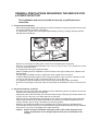
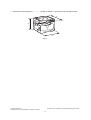
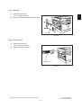
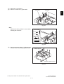
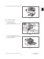
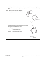
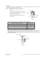
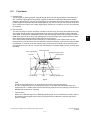
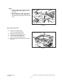
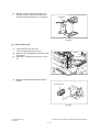
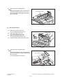
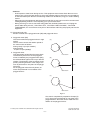
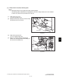
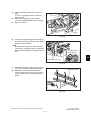
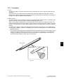
1) Transportation/Installation
- When transporting/installing the equipment, remove the drawer, employ two persons and be sure
to hold the positions as shown in the figure.
The equipment is quite heavy and weighs approximately 32.5 kg (71.65 lb), therefore pay full
attention when handling it.
-
Be sure not to hold the movable parts or units when transporting the equipment.
Be sure to use a dedicated outlet with AC 110 V / 13.2 A, 115 V or 127 V / 12 A, 220-240 V or 240
V / 8 A for its power source.
The equipment must be grounded for safety.
Select a suitable place for installation. Avoid excessive heat, high humidity, dust, vibration and
direct sunlight.
Provide proper ventilation since the equipment emits a slight amount of ozone.
To insure adequate working space for the copying operation, keep a minimum clearance of 80
cm (32”) on the left, 80 cm (32”) on the right and 10 cm (4”) on the rear.
The equipment shall be installed near the socket outlet and shall be easily accessible.
Be sure to fix and plug in the power cable securely after the installation so that no one trips over
it.
2) General Precautions at Service
- Be sure to turn the power OFF and unplug the power cable during service (except for the service
should be done with the power turned ON).
- Unplug the power cable and clean the area around the prongs of the plug and socket outlet once
a year or more. A fire may occur when dust lies on this area.
- When the parts are disassembled, reassembly is the reverse of disassembly unless otherwise
noted in this manual or other related documents. Be careful not to install small parts such as
screws, washers, pins, E-rings, star washers in the wrong places.
- Basically, the equipment should not be operated with any parts removed or disassembled.
- The PC board must be stored in an anti-electrostatic bag and handled carefully using a wristband
since the ICs on it may be damaged due to static electricity.
Caution: Before using the wristband, unplug the power cable of the equipment and
make sure that there are no charged objects which are not insulated in the
vicinity.
-
-
-
-
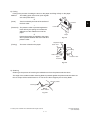
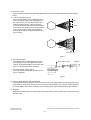
Avoid expose to laser beam during service. This equipment uses a laser diode. Be sure not to
expose your eyes to the laser beam. Do not insert reflecting parts or tools such as a screwdriver
on the laser beam path. Remove all reflecting metals such as watches, rings, etc. before starting
service.
Be sure not to touch high-temperature sections such as the exposure lamp, fuser unit, damp
heater and areas around them.
Be sure not to touch high-voltage sections such as the chargers, developer, high-voltage transformer and power supply unit. Especially, the board of these components should not be touched
since the electric charge may remain in the capacitors, etc. on them even after the power is
turned OFF.
Make sure that the equipment will not operate before touching potentially dangerous places (e.g.
rotating/operating sections such as gears, belts pulleys, fans and laser beam exit of the laser
optical unit).
Be careful when removing the covers since there might be the parts with very sharp edges
underneath.
When servicing the equipment with the power turned ON, be sure not to touch live sections and
rotating/operating sections. Avoid exposing your eyes to laser beam.
Use designated jigs and tools.
Use recommended measuring instruments or equivalents.
Return the equipment to the original state and check the operation when the service is finished.
3) Important Service Parts for Safety
- The breaker, door switch, fuse, thermostat, thermofuse, thermistor, batteries, IC-RAMs including
lithium batteries, etc. are particularly important for safety. Be sure to handle/install them properly.
If these parts are short-circuited and their functions become ineffective, they may result in fatal
accidents such as burnout. Do not allow a short-circuit or do not use the parts not recommended
by Toshiba TEC Corporation.
4) Cautionary Labels
- During servicing, be sure to check the rating plate and cautionary labels such as “Unplug the
power cable during service”, “CAUTION. HOT”, “CAUTION. HIGH VOLTAGE”, “CAUTION.
LASER BEAM”, etc. to see if there is any dirt on their surface and if they are properly stuck to the
equipment.
5) Disposal of the Equipment, Supplies, Packing Materials, Used Batteries and IC-RAMs
- Regarding the recovery and disposal of the equipment, supplies, packing materials, used batteries and IC-RAMs including lithium batteries, follow the relevant local regulations or rules.
Caution:
Dispose of used batteries and IC-RAMs including lithium batteries according to this manual.
Attention:
Se débarrasser de batteries et IC-RAMs usés y compris les batteries en lithium selon ce manuel.
Vorsicht:
Entsorgung der gebrauchten Batterien und IC-RAMs (inclusive der Lithium-Batterie) nach diesem Handbuch.
CONTENTS
e-STUDIO167/207/237
1. SPECIFICATIONS / ACCESSORIES / OPTIONS / SUPPLIES ................................... 1-1
1.1
1.2
1.3
1.4
1.5
Specifications....................................................................................................................... 1-1
Accessories ......................................................................................................................... 1-5
Options ................................................................................................................................ 1-6
Supplies ............................................................................................................................... 1-7
System List .......................................................................................................................... 1-8
2. OUTLINE OF THE MACHINE ....................................................................................... 2-1
2.1
2.2
2.3
2.4
Sectional View ..................................................................................................................... 2-1
Electric Parts Layout............................................................................................................ 2-4
Symbols and Functions of Various Components............................................................... 2-11
General Description ........................................................................................................... 2-15
2.4.1 System block diagram ............................................................................................ 2-15
2.4.2 Construction of boards ........................................................................................... 2-16
2.5 Disassembly and Replacement of Covers......................................................................... 2-18
2.6 Disassembly and Replacement of PC boards ................................................................... 2-23
2.7 Removal and Installation of Options .................................................................................. 2-29
3. COPY PROCESS .......................................................................................................... 3-1
3.1 General Description of Copying Process............................................................................. 3-1
3.2 Details of Copying Process.................................................................................................. 3-2
3.3 Comparison with e-STUDIO230/280 ................................................................................. 3-13
4. GENERAL OPERATION............................................................................................... 4-1
4.1 Overview of Operation ......................................................................................................... 4-1
4.2 Description of Operation ...................................................................................................... 4-2
4.2.1 Warming-up .............................................................................................................. 4-2
4.2.2 Ready state (ready for copying) ............................................................................... 4-2
4.2.3 Drawer feed copying ................................................................................................ 4-3
4.2.4 Bypass feed copying ................................................................................................ 4-4
4.2.5 Interruption copying .................................................................................................. 4-4
4.3 Detection of Abnormality...................................................................................................... 4-5
4.3.1 Types of abnormality ................................................................................................ 4-5
4.3.2 Description of abnormality ........................................................................................ 4-6
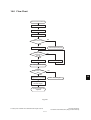
4.4 Flow Chart ......................................................................................................................... 4-11
4.4.1 Immediately after the power is turned ON .............................................................. 4-11
4.4.2 Automatic paper feed copying ................................................................................ 4-13
5. CONTROL PANEL........................................................................................................ 5-1
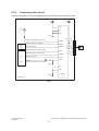
5.1 General Description ............................................................................................................ 5-1
5.2 Items Shown on the Display Panel ...................................................................................... 5-2
5.2.1 Display...................................................................................................................... 5-2
5.2.2 Message ................................................................................................................... 5-3
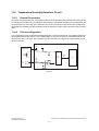
5.3 Relation between Equipment State and Operation.............................................................. 5-4
5.4 Operation ............................................................................................................................. 5-5
5.4.1 Block diagram........................................................................................................... 5-5
5.4.2 LED display circuit .................................................................................................... 5-6
5.5 Disassembly and Replacement ........................................................................................... 5-7
6. SCANNER ..................................................................................................................... 6-1
6.1
6.2
6.3
6.4
General Description ............................................................................................................. 6-1
Construction......................................................................................................................... 6-2
Functions ............................................................................................................................. 6-3
Description of Operation ...................................................................................................... 6-5
© February 2007 TOSHIBA TEC CORPORATION All rights reserved
e-STUDIO167/207/237
CONTENTS
1
6.4.1 Scanning operation .................................................................................................. 6-5
6.4.2 Scan motor drive circuit ............................................................................................ 6-6
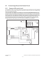
6.5 Contact Image Sensor Unit Control Circuit.......................................................................... 6-8
6.5.1 Exposure LED control circuit .................................................................................... 6-8
6.5.2 CCD control circuit ................................................................................................... 6-9
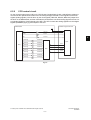
6.6 Automatic Original Size Detection Circuit .......................................................................... 6-12
6.6.1 Principle of original size detection .......................................................................... 6-12
6.6.2 Process of detection of original size ....................................................................... 6-13
6.7 Disassembly and Replacement ......................................................................................... 6-17
7. IMAGE PROCESSING .................................................................................................. 7-1
7.1 General Description ............................................................................................................. 7-1
7.2 Configuration ....................................................................................................................... 7-2
7.3 MAIN Board ......................................................................................................................... 7-3
7.3.1 Features ................................................................................................................... 7-3
7.3.2 Functions of image processing circuit ...................................................................... 7-4
8. LASER OPTICAL UNIT ................................................................................................ 8-1
8.1
8.2
8.3
8.4
8.5
General Description ............................................................................................................. 8-1
Structure .............................................................................................................................. 8-2
Laser Diode Control Circuit.................................................................................................. 8-5
Polygonal Motor Control Circuit ........................................................................................... 8-6
Disassembly and Replacement ........................................................................................... 8-7
9. DRIVE UNIT .................................................................................................................. 9-1
9.1
9.2
9.3
9.4
9.5
General Description ............................................................................................................. 9-1
Configuration ....................................................................................................................... 9-2
Functions ............................................................................................................................ 9-3
Main Motor Control Circuit ................................................................................................... 9-4
Disassembly and Replacement ........................................................................................... 9-6
10. PAPER FEEDING SYSTEM........................................................................................ 10-1
10.1
10.2
10.3
10.4
General Description ........................................................................................................... 10-1
Configuration ..................................................................................................................... 10-2
Functions ........................................................................................................................... 10-3
Operation ........................................................................................................................... 10-5
10.4.1 Drawer .................................................................................................................... 10-5
10.4.2 Bypass tray............................................................................................................. 10-7
10.4.3 General operation................................................................................................... 10-9
10.5 Disassembly and Replacement ....................................................................................... 10-10
11. DRUM RELATED SECTION ....................................................................................... 11-1
11.1
11.2
11.3
11.4
General Description ........................................................................................................... 11-1
Configuration ..................................................................................................................... 11-2
Functions ........................................................................................................................... 11-3
High-Voltage Output Control Circuit .................................................................................. 11-5
11.4.1 General description ................................................................................................ 11-5
11.4.2 Description of Operation......................................................................................... 11-6
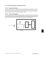
11.5 Drum Temperature Detection Circuit ................................................................................. 11-7
11.5.1 General description ................................................................................................ 11-7
11.5.2 Circuit configuration................................................................................................ 11-7
11.6 Temperature/Humidity Detection Circuit............................................................................ 11-8
11.6.1 General Description................................................................................................ 11-8
11.6.2 Circuit configuration................................................................................................ 11-8
11.7 Disassembly and Replacement ......................................................................................... 11-9
12. DEVELOPMENT SYSTEM.......................................................................................... 12-1
12.1 General Description ........................................................................................................... 12-1
e-STUDIO167/207/237
CONTENTS
© February 2007 TOSHIBA TEC CORPORATION All rights reserved
2
12.2 Construction....................................................................................................................... 12-2
12.3 Functions ........................................................................................................................... 12-3
12.3.1 Function of each unit .............................................................................................. 12-3
12.3.2 Functions of the toner cartridge PC board (CTRG) ................................................ 12-4
12.3.3 Recovered toner supply mechanism ...................................................................... 12-6
12.4 Toner Motor Control Circuit ............................................................................................... 12-7
12.5 Auto-Toner Circuit.............................................................................................................. 12-8
12.5.1 General description ................................................................................................ 12-8
12.5.2 Function of auto-toner sensor ................................................................................ 12-9
12.6 Disassembly and Replacement ....................................................................................... 12-11
13. FUSER / EXIT UNIT .................................................................................................... 13-1
13.1
13.2
13.3
13.4
13.5
General Description ........................................................................................................... 13-1
Configurations.................................................................................................................... 13-2
Functions ........................................................................................................................... 13-3
Operation ........................................................................................................................... 13-5
Fuser Unit Control Circuit .................................................................................................. 13-6
13.5.1 Configuration .......................................................................................................... 13-6
13.5.2 Temperature detection section ............................................................................... 13-7
13.6 Disassembly and Replacement ....................................................................................... 13-12
14. AUTOMATIC DUPLEXING UNIT (ADU) (OPTION: MD-0103) .................................. 14-1
14.1 General Description ........................................................................................................... 14-1
14.1.1 Specifications of MD-0103 ..................................................................................... 14-2
14.2 Construction....................................................................................................................... 14-3
14.3 Functions ........................................................................................................................... 14-4
14.4 Drive of ADU...................................................................................................................... 14-5
14.5 Description of Operation ................................................................................................... 14-6
14.6 Flow Chart ....................................................................................................................... 14-11
14.7 Disassembly and Replacement ....................................................................................... 14-12
15. POWER SUPPLY UNIT .............................................................................................. 15-1
15.1
15.2
15.3
15.4
15.5
15.6
15.7
Construction....................................................................................................................... 15-1
Operation of DC Output Circuit.......................................................................................... 15-2
Output Channel ................................................................................................................. 15-3
Fuse................................................................................................................................... 15-4
Configuration of Power Supply Unit................................................................................... 15-5
Power Supply Sequence ................................................................................................... 15-6
AC Wire Harness ............................................................................................................... 15-7
16. PC BOARDS ............................................................................................................... 16-1
© February 2007 TOSHIBA TEC CORPORATION All rights reserved
e-STUDIO167/207/237
CONTENTS
3
e-STUDIO167/207/237
CONTENTS
© February 2007 TOSHIBA TEC CORPORATION All rights reserved
4
1.
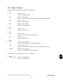
SPECIFICATIONS / ACCESSORIES / OPTIONS / SUPPLIES
1.1
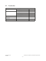
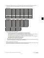
Specifications
Copy process
Type
Original table
!Accepted originals
Indirect electrophotographic process (dry)
Desktop type
Fixed type (the left rear corner used as guide to place originals)
Sheet, book and 3-dimensional object. The automatic document feeder
(ADF) and reversing automatic document feeder (RADF), only accepts paper
which are not pasted or stapled. (Single-sided originals: 50 to 127 g/m2/13 to
34 lb. Bond) Carbon paper are not acceptable either.
Maximum size: A3/LD
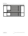
!Copy speed (Copies/min.)
e-STUDIO167
Bypass feed
Paper size
Drawer
Size specified
PFP
Size not
specified
PFU
Upper
drawer
Lower
drawer
A4, B5, LT
16
16
11
16
16
16
A5-R, ST-R
-
16
11
-
16
16
15.5
15.5
11
15.5
15.5
15.5
13
13
11
13
13
13
11
11
11
11
11
11
Size not
specified
PFU
Upper
drawer
Lower
drawer
20
A4-R, B5-R, LT-R
B4, LG, FOLIO,
COMPUTER
A3, LD
e-STUDIO207
Bypass feed
Paper size
PFP
Drawer
Size specified
A4, B5, LT
20
20
20
20
20
A5-R, ST-R
-
-
20
-
20
20
15.5
15.5
15.5
15.5
15.5
15.5
B4, LG, FOLIO,
COMPUTER
13
13
13
13
13
13
A3, LD
11
11
11
11
11
11
Drawer
Size specified
Size not
specified
PFU
Upper
drawer
Lower
drawer
A4, B5, LT
23
23
23
23
23
23
A5-R, ST-R
-
-
23
-
23
23
17.5
17.5
17.5
17.5
17.5
17.5
15
15
15
15
15
15
12.5
12.5
12.5
12.5
12.5
12.5
A4-R, B5-R, LT-R
e-STUDIO237
Bypass feed
Paper size
A4-R, B5-R, LT-R
B4, LG, FOLIO,
COMPUTER
A3, LD
*
*
PFP
“–” means “Not acceptable”.
The copy speed in the above table are available when originals are manually placed for single side,
multiple copying.
© February 2007 TOSHIBA TEC CORPORATION All rights reserved
e-STUDIO167/207/237
SPECIFICATIONS / ACCESSORIES / OPTIONS / SUPPLIES
1-1
1
*
When the ADF and RADF are used, the copy speed of 16/20/23 sheets per minute is only available
under the following conditions:
• Original/Mode:
Single side original/A4/LT size. APS/automatic density are not selected.
• Number of sheets:
16 or more. (e-STUDIO167)
20 or more. (e-STUDIO207)
23 or more. (e-STUDIO237)
• Reproduction ratio: 100%
Copy speed for thick paper (Copies/min.)
e-STUDIO167/207/237
Thick 1 (81 g/m2 to 105 g/m2, 21.3 lb. Bond to 28 lb. Bond): Bypass feed on a sheet by sheet baisis
only
Thick 2 (106 g/m2 to 163 g/m2, 28 lb. Bond to 90 lb. Index): Bypass feed on a sheet by sheet baisis only
!Copy paper
Drawer
PFU
PFP
ADU
Bypass copy
A3 to A5-R, LD to ST-R,
FOLIO, COMPUTER, 13"LG,
8.5" x 8.5", 8K, 16K, 16K-R
(Non-standard or user-specified sizes can be set.)
Remarks
Size
A3, A4, A4-R, B4, B5, B5-R,
A5-R(Only for PFP), LD, LG, LT, LT-R,
ST-R(Only for PFP), FOLIO, COMPUTER,
13"LG, 8K, 16K, 16K-R
Weight
64 to 80 g/m2, 17 lb. Bond to 21.3 lb. Bond
50 to 163 g/m2
(Single paper feeding)
64 to 80 g/m2
(Continuous feeding)
Special
paper
–
Tracing paper, labels, OHP film These special papers
(thickness: 80 µm or thicker),
recommended by
Toshiba Tec
!First copy time ..................... Approx. 7.6 sec.
(A4, 100%, original placed manually, e-STUDIO167/207)
Approx. 7.5 sec.
(A4, 100%, original placed manually, e-STUDIO237)
Approx. 7.7 sec.
(LT, 100%, original placed manually, e-STUDIO167/207)
Approx. 7.5 sec. |
(LT, 100%, original placed manually, e-STUDIO237)
Approx. 7.7 sec.
(LT, 100%, original placed manually)
!Warming-up time.................. Approx. 25 sec. (temperature: 20°C)
!Multiple copying ................... Up to 999 copies; Key in set numbers
!Reproduction ratio ............... Actual ratio: 100±0.5%
Zooming: 25 to 200% in increments of 1%
!Resolution/Gradation ........... Scanning: 600 dpi x 600 dpi
Printing: Equivalent to 2400 dpi x 600 dpi
Gradation: 256 steps
!Eliminated portion ................ Leading edges: 3.0±2.0 mm, Side/trailing edges: 2.0±2.0 mm (copy)
Leading / trailing edges: 5.0±2.0 mm, Side edges: 5.0±2.0 mm (print)
e-STUDIO167/207/237
SPECIFICATIONS / ACCESSORIES / OPTIONS / SUPPLIES
© February 2007 TOSHIBA TEC CORPORATION All rights reserved
1-2
Paper feeding ......................... Standard drawer:
1 drawer (stack height 28 mm, equivalent to 250 sheets; 64 to 80 g/m2
(17 to 22 lb. Bond))
Bypass feeding:
Stack height 11.8 mm: equivalent to 100 sheets; 64 to 80 g/m2 (17 to
22 lb. Bond)
Paper Feed Unit (PFU):
Option (One drawer: stack height 28 mm, equivalent to 250 sheets; 64
to 80 g/m2 (17 to 22 lb. Bond))
Paper Feed Pedestal (PFP):
Option (One drawer or two: stack height 60.5 mm, equivalent to 550
sheets; 64 to 80 g/m2 (17 to 22 lb. Bond))
Capacity of originals in the ADF/RADF (Option)
.................................................. A3 to A5-R, LD to ST-R:
100 sheets / 80 g/m2 (Stack height 16 mm or less)
Automatic duplexing unit (ADU: Option)
.................................................. Stackless, Switchback type
Toner supply ........................... Automatic toner density detection/supply
Toner cartridge replacing method (There is a recovered toner supply
mechanism.)
!Density control ..................... Automatic density mode and manual density mode selectable in 7
steps
!Weight.................................. Approximately 32.5 kg (71.65 lb.) (excluding the developer material
and toner)
!Power requirements...AC 110 V / 13.2 A, 115 V or 127 V / 12 A
220-240 V or 240 V / 8 A (50/60 Hz)
* The acceptable value of each voltage is ±10%.
!Power consumption ...1.5 kW or less (100 V series)
1.6 kW or less (200 V series)
* The electric power is supplied to the ADF/RADF, PFU, PFP and ADU through the equipment.
!Total counter ..............Electronical counter
© February 2007 TOSHIBA TEC CORPORATION All rights reserved
e-STUDIO167/207/237
SPECIFICATIONS / ACCESSORIES / OPTIONS / SUPPLIES
1-3
1
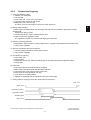
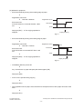
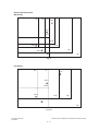
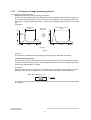
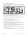
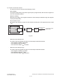
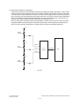
!Dimensions of the equipment .................. W 600 x D 658.6 x H 462.5 (mm): See the figure below
D
H
W
Fig. 1-1
e-STUDIO167/207/237
SPECIFICATIONS / ACCESSORIES / OPTIONS / SUPPLIES
© February 2007 TOSHIBA TEC CORPORATION All rights reserved
1-4
1.2
*
Accessories
1
Unpacking/setup instruction
1 set
Operator’s manual
1 pc.
Operator’s manual pocket
1 pc. (for NAD)
Power cable
1 pc.
CD-ROM
2 pcs.
Rubber cap
6 pcs. (for MJD, ASD, ASU and SAD)
2 pcs. (for NAD, CND, AUD, TWD, KRD and ARD)
Transfer charger wire cleaner
(installed inside of the transfer cover)
1 pc.
Drum (installed inside of the equipment)
1 pc.
Developer material
1 pc.
Nozzle
1 pc. (for NAD)
Toner cartridge
1 pc.
Warranty sheet
1 pc. (for NAD and CND)
Setup report
1 set (for NAD, MJD and CND)
Customer satisfaction card
1 pc. (for MJD)
Packing list
1 pc. (for CND)
Customer survey sheet
1 pc. (for CND)
Certificate of conformance
1 pc. (for CND)
Machine version
NAD:
North America
ASD:
Hong Kong / Latin America
AUD:
Australia
MJD:
Europe
ASU:
Asia / Saudi Arabia
SAD:
Saudi Arabia
ARD:
Latin America
CND:
China
TWD:
Taiwan
KRD:
Korea
JPD:
Japan
© February 2007 TOSHIBA TEC CORPORATION All rights reserved
e-STUDIO167/207/237
SPECIFICATIONS / ACCESSORIES / OPTIONS / SUPPLIES
1-5
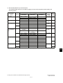
07/03
1.3
Options
Platen Cover
KA-1640PC/C
Automatic Document Feeder (ADF)
MR-2017/C
Reversing Automatic Document Feeder (RADF)
MR-3019/C
Paper Feed Unit (PFU)
MY-1027/C
Paper Feed Pedestal (PFP)
KD-1022/C
Paper Feed Controller (PFC)
GH-1060/C
Drawer Module
MY-1028/C
Automatic Duplexing Unit (ADU)
MD-0103/C
Fax Kit
GD-1220NA/EU/AU/TW/CN/KR
External Keyboard
GJ-1040/C/EU/KR/TW
Network Printer Kit
GA-1190/C/KR/TW
Scanner Upgrade Kit
GA-1200/C/KR/TW
Operator’s manual pocket
KK-1660/C
Damp Heater
MF-1640U/E
Harness Kit
GQ-1130
Desk
MH-1640
Notes:
• When the paper feed pedestal (KD-1022) or automatic duplexing unit (MD-0103) is installed,
the paper feed controller (GH-1060) is also required to be installed.
• The external keyboard (GJ-1040) is necessary for the installation of the fax kit (GD-1220) and
the scanner upgrade kit (GA-1200).
e-STUDIO167/207/237
SPECIFICATIONS / ACCESSORIES / OPTIONS / SUPPLIES
© February 2007 TOSHIBA TEC CORPORATION All rights reserved
1-6
1.4
Supplies
1
Drum
OD-1600 (except for China)
OD-2320 (for China)
Toner cartridge
PS-ZT1640 (4) (for North America)
PS-ZT1640D (4) (for Asia, Central and South America)
PS-ZT1640D5K (4) (for Asia, Central and South America)
PS-ZT1640C (4) (for China)
PS-ZT1640C5K (4) (for China)
PS-ZT1640T (4) (for Taiwan)
PS-ZT1640T5 (4) (for Taiwan)
PS-ZT1640E (1) (for Europe)
PS-ZT1640E5K (1) (for Europe)
Developer material
D-2320 (except for China)
D-2320C (for China)
© February 2007 TOSHIBA TEC CORPORATION All rights reserved
e-STUDIO167/207/237
SPECIFICATIONS / ACCESSORIES / OPTIONS / SUPPLIES
1-7
Fax Kit
GD-1220
Harness Kit
GQ-1130
e-STUDIO167/207/237
SPECIFICATIONS / ACCESSORIES / OPTIONS / SUPPLIES
1-8
Drawer Module
MY-1028
Scanner
Upgrade Kit
GA-1200
Network
Printer Kit
GA-1190
Damp Heater
MF-1640
External Keyboard
GJ-1040
Platen Cover
KA-1640PC
Paper Feed
Pedestal
(PFP)
KD-1022
Automatic
Document Feeder
(ADF)
MR-2017
Desk
MH-1640
Paper Feed Unit
(PFU)
MY-1027
Paper Feed
Controller
(PFC)
GH-1060
Automatic
Duplexing Unit
(ADU)
MD-0103
Reversing Automatic
Document Feeder
(RADF)
MR-3019
1.5
System List
Fig. 1-2
© February 2007 TOSHIBA TEC CORPORATION All rights reserved
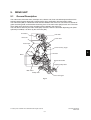
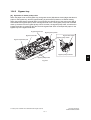
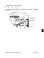
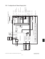
2.
OUTLINE OF THE MACHINE
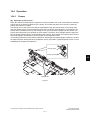
2.1
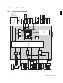
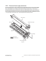
Sectional View
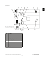
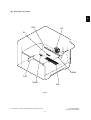
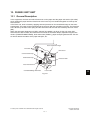
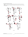
2
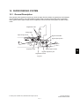
1) Front side
A2 A3
A4
A1
A7
A5
A6
K5
J3
J9
J1
J2
L3
L1
I7
H4
H5
H1
G2
G1
G3
L3
I1
I2
C5
L2
E2
E1
J6 J7 J5 J4 J8
K2 I5 I9 F3 F2 F1
K4
K3
B2
B1
K1
F4 I8 I4
H2 H3
I11 I10 I3 I6 C3
C1 C2 C4 E3
E5
E4
Fig. 2-1
A1
Original glass
A2
ADF original glass
A3
Contact image sensor unit (CIS)
A4
Scanner damp heater (Left side)
DH1
A5
Scanner damp heater (Right side)
DH2
A6
Scanner damp heater thermostat
THMO2
A7
Automatic original detection sensor
S9-S13
B1
Laser optical unit
B2
Polygonal motor
C1
Pickup roller
M4
C2
Separation claw
C3
Paper empty sensor
S7
C4
Registration sensor
S4
C5
Registration roller
E1
Bypass pickup roller
© February 2007 TOSHIBA TEC CORPORATION All rights reserved
e-STUDIO167/207/237
OUTLINE OF THE MACHINE
2-1
E2
Bypass feed roller
E3
Bypass separation pad
E4
Bypass paper sensor
E5
Bypass tray
F1
Needle electrode
F2
Main charger
F3
Main charger grid
F4
Toner cartridge
G1
Transfer charger wire
G2
Separation charger wire
G3
Transfer guide roller
H1
Drum
H2
Discharge LED
H3
Drum cleaning blade
H4
Recovery blade
H5
Drum separation finger
I1
Developer sleeve (Magnetic roller)
I2
Mixer-1
I3
Mixer-2
S8
I4
Mixer-3
I5
Doctor blade
I6
Auto-toner sensor
I7
Toner recovery auger
I8
Toner recycle auger
I9
Drum thermistor
THMS4
I10
Drum damp heater
DH3
I11
Drum damp heater thermostat
THMO3
J1
Fuser roller
J2
Pressure roller
J3
Fuser roller separation finger
J4
Center heater lamp
S6
LAMP1
J5
Side heater lamp
LAMP2
J6
Center/Side/Edge thermistor
THMS1/2/3
J7
Fuser thermostat
THMO1
J8
Exit roller
J9
Exit sensor
S5
K1
Front cover opening/closing switch
SW4
K2
Front cover opening/closing interlock switch
SW3
K3
Temperature/humidity sensor
S3
K4
Switching regulator
K5
ADU cover opening/closing interlock switch
L1
ADU upper transport roller
L2
ADU lower transport roller
L3
ADU paper guide
SW2
e-STUDIO167/207/237
OUTLINE OF THE MACHINE
© February 2007 TOSHIBA TEC CORPORATION All rights reserved
2-2
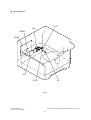
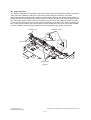
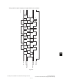
2) Rear side
M1
M5
M7
M2
S2
S1
2
M8
SOL2 CLT1
SOL1 SW5
M3
M6
Fig. 2-2
M1
Scan motor
M2
Toner motor
M3
Main motor
M5
Exhaust fan
M6
Switching regulator cooling fan
M7
Exit motor (Option)
M8
ADU motor (Option)
S1
CIS home position sensor
S2
Platen sensor
SW5
Drawer detection switch
CLT1
Registration clutch
SOL1
Pickup solenoid
SOL2
Bypass pickup solenoid
© February 2007 TOSHIBA TEC CORPORATION All rights reserved
e-STUDIO167/207/237
OUTLINE OF THE MACHINE
2-3
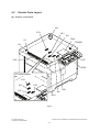
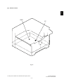
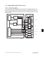
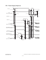
2.2
Electric Parts Layout
[A] Scanner, control panel
M1
S13
S12
S11
DH2
S1
THMO2
S2
LCD
CIS
HPNL
LT series models
S13
S12
S10
S10
S11
S9
DH1
Fig. 2-3
e-STUDIO167/207/237
OUTLINE OF THE MACHINE
© February 2007 TOSHIBA TEC CORPORATION All rights reserved
2-4
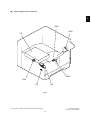
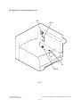
[B] Power supply section, switches
2
SW3
SW2
PS
SW4
SW1
M6
S3
Fig. 2-4
© February 2007 TOSHIBA TEC CORPORATION All rights reserved
e-STUDIO167/207/237
OUTLINE OF THE MACHINE
2-5
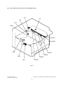
[C] Laser optical unit, fuser unit, toner cartridge section
M7
S5
M2
CTIF
CTRG
LAMP1
LAMP2
SNS
THMO1
THMS1
LDR
THMS2
M4
THMS3
Fig. 2-5
e-STUDIO167/207/237
OUTLINE OF THE MACHINE
© February 2007 TOSHIBA TEC CORPORATION All rights reserved
2-6
[D] Developer unit section
2
ERS
M5
S6
THMS4
FUS
THMO3
DH3
Fig. 2-6
© February 2007 TOSHIBA TEC CORPORATION All rights reserved
e-STUDIO167/207/237
OUTLINE OF THE MACHINE
2-7
[E] Driving section
CLT1
M3
SRAM
MAIN
PFC
S4
SOL1
Fig. 2-7
e-STUDIO167/207/237
OUTLINE OF THE MACHINE
© February 2007 TOSHIBA TEC CORPORATION All rights reserved
2-8
[F] Drawer section
2
SW5
S7
Fig. 2-8
© February 2007 TOSHIBA TEC CORPORATION All rights reserved
e-STUDIO167/207/237
OUTLINE OF THE MACHINE
2-9
[G] Bypass unit, automatic duplexing unit
M8
ADU
S8
SOL2
Fig. 2-9
e-STUDIO167/207/237
OUTLINE OF THE MACHINE
© February 2007 TOSHIBA TEC CORPORATION All rights reserved
2 - 10
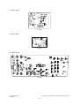
2.3
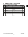
Symbols and Functions of Various Components
The column "P-I" shows the page and item number in the parts list.
1) Motors
Symbol
Name
Function
Remarks
P-I
M1
SCAN-MOT
Scan motor
Driving the CIS
Fig. 2-3
10-1
M2
TNR-MOT
Toner motor
Supplying the toner
Fig. 2-5
12-15
M3
MAIN-MOT
Main motor
Driving the drum, developer unit, registration roller, Pickup roller, feed roller,
cleaner unit
Fig. 2-7
12-2
M4
M/DC-POL
Polygonal motor
Driving the polygonal mirror
Fig. 2-5
5-13
M5
EXT-FAN-MOT
Exhaust fan
Exhausting ozone and cooling down
the equipment inside
Fig. 2-6
11-23
M6
PS-FAN-MOT
Switching regulator cooling fan
Cooling down the switching regulator
Fig. 2-4
5-11
M7
EXIT-MOT
Exit motor
Driving the fuser unit and exit roller
* Option
Fig. 2-5
MD-0103
2-2
M8
ADU-MOT
ADU motor
Driving the automatic duplexing unit
* Option
Fig. 2-9
MD-0103
1-23
© February 2007 TOSHIBA TEC CORPORATION All rights reserved
e-STUDIO167/207/237
OUTLINE OF THE MACHINE
2 - 11
2
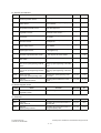
2) Sensors and switches
Symbol
Name
Function
Remarks
P-I
S1
HOME-SNR
CIS home position sensor
Detecting CIS home position
Fig. 2-3
10-106
S2
PLTN-SNR
Platen sensor
Detecting the opening/closing of platen
cover or RADF
Fig. 2-3
9-101
S3
TEMP/HUMI-SNR
Temperature/humidity sensor
Detecting the temperature and humidity
inside the equipment
Fig. 2-4
5-16
S4
RGST-SNR
Registration sensor
Detecting the transporting paper at the
registration roller section
Fig. 2-7
15-107
S5
EXIT-SNR
Exit sensor
Detecting the transporting paper at the
exit section
Fig. 2-5
24-8
S6
ATTNR-SNR
Auto-toner sensor
Detecting the density of toner in the
developer unit
Fig. 2-6
21-46
S7
EMP-SNR
Paper empty sensor
Detecting presence/absence of paper
in the drawer
Fig. 2-8
15-107
S8
SFB-SNR
Bypass paper sensor
Detecting presence/absence of paper
on the bypass tray
Fig. 2-9
13-101
S9-13
APS 1-3, APS-C, APS-R
Automatic original detection sensor
Detecting original size
* S9: only for A4 series models
Fig. 2-3
9-9,
9-19
SW1
MAIN-SW
Main switch
Turning ON/OFF of the equipment
Fig. 2-4
5-4
SW2
ADU-COV-INTLCK-SW
ADU cover opening/closing interlock
switch
Controlling cutoff and supply of the 24V
voltage by opening/closing of the ADU
cover
Fig. 2-4
6-8
SW3
FRNT-COV-INTLCK-SW
Front cover opening/closing interlock
switch
Controlling cutoff and supply of the 24V
voltage by opening/closing of the front
cover
Fig. 2-4
1-5
SW4
FRNT-COV-SW
Front cover opening/closing switch
Detecting the opening/closing of the
front cover
Fig. 2-4
1-101
SW5
CST-SW
Drawer detection switch
Detecting presence/absence of the
drawer
Fig. 2-8
16-110
Remarks
P-I
Fig. 2-7
16-21
Remarks
P-I
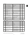
3) Electromagnetic clutch
Symbol
CLT1
Name
RGST-CLT
Registration clutch
Function
Driving the registration roller
4) Solenoids
Symbol
Name
Function
SOL1
CST-SOL
Pickup solenoid
Controlling the power transmission of
the feed roller
Fig. 2-7
16-9
SOL2
SFB-SOL
Bypass pickup solenoid
Controlling the power transmission of
the bypass pickup roller
Fig. 2-9
14-15
e-STUDIO167/207/237
OUTLINE OF THE MACHINE
© February 2007 TOSHIBA TEC CORPORATION All rights reserved
2 - 12
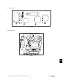
5) PC boards
Symbol
MAIN
Name
Function
Remarks
P-I
7-1
PWA-F-MAIN
Main PC board (MAIN board)
Controlling the whole system and
image processing
Fig. 2-7
PWA-F-SRAM
SRAM PC board (SRAM board)
Storing the setting information of the
equipment
Fig. 2-7
7-33
LDR
PWA-F-LDR
Laser driving PC board (LDR board)
Driving the laser diode
Fig. 2-5
5-13
SNS
PWA-F-SNS
H-sync signal detection PC board
(SNS board)
Detecting the laser beam position
Fig. 2-5
5-13
HPNL
PWA-F-HPNL
Control panel PC board
(HPNL board)
Detecting the button entry and controlling LED and LCD on the control panel
Fig. 2-3
4-20
CTIF
PWA-F-CTIF
Toner cartridge interface PC board
(CTIF board)
Interface for detecting the toner cartridge
(Detecting the CTRG board)
Fig. 2-5
7-30
CTRG
PWA-F-CTRG
Toner cartridge PC board
(CTRG board)
Storing the status of the toner cartridge
Fig. 2-5
103-3
FUS
PWA-F-FUS
Fuse PC board (FUS board)
Supplying power to each damp heater
* Optional for NAD/MJD/CND model,
standard for other models
Fig. 2-6
7-12
PFC
PWA-F-PFC
Paper feed controller PC board
(PFC board)
Controlling the automatic duplexing unit
and paper feed pedestal
* Option
Fig. 2-7
7-35
ADU
PWA-F-ADU
ADU driving PC board (ADU board)
Controlling the automatic duplexing unit
* Option
Fig. 2-9
MD-0103
1-13
Function
Remarks
P-I
SRAM
2
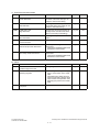
6) Lamps and heaters
Symbol
Name
LAMP1
CNTR-LAMP
Center heater lamp
Heating the center section of the fuser
roller
Fig. 2-5
23-12
LAMP2
SIDE-LAMP
Side heater lamp
Heating the section of both sides of the
fuser roller
Fig. 2-5
23-13
ERS
LP-ERS
Discharge LED
Removing the residual charge from the
drum surface
Fig. 2-6
20-13
DH1
SCN-DH-L
Scanner damp heater (Left)
Preventing condensation in the scanner unit
* Optional for NAD/MJD/CND model,
standard for other models
Fig. 2-3
9-17
DH2
SCN-DH-R
Scanner damp heater (Right)
Preventing condensation in the scanner unit
* Optional for NAD/MJD/CND model,
standard for other models
Fig. 2-3
9-18
DH3
DRM-DH
Drum damp heater
Preventing condensation of the drum
* Optional for NAD/MJD/CND model,
standard for other models
Fig. 2-6
8-6
© February 2007 TOSHIBA TEC CORPORATION All rights reserved
e-STUDIO167/207/237
OUTLINE OF THE MACHINE
2 - 13
7) Thermistors and thermostats
Symbol
Name
Function
Remarks
P-I
THMS1
THMS-C-HTR
Center thermistor
Detecting the surface temperature at
the center of the fuser roller (for controlling the center heater lamp)
Fig. 2-5
23-6
THMS2
THMS-S-HTR
Side thermistor
Detecting the surface temperature at
the rear side of the fuser roller (for controlling the side heater lamp)
Fig. 2-5
23-6
THMS3
THMS-EDG-HTR
Edge thermistor
Detecting the surface temperature at
the edge of the rear side of the fuser
roller (for preventing overheating)
Fig. 2-5
23-6
THMS4
THMS-DRM
Drum thermistor
Detecting the temperature on the drum
surface
Fig. 2-6
21-49
THMO1 THERMO-FSR
Fuser thermostat
Preventing overheating in the fuser unit
Fig. 2-5
23-5
THMO2 THERMO-SCN-DH
Scanner damp heater thermostat
Preventing overheating in the scanner
damp heater
* Optional for NAD/MJD/CND model,
standard for other models
Fig. 2-3
9-20
THMO3 THERMO-DRM-DH
Drum damp heater thermostat
Preventing overheating in the drum
damp heater
* Optional for NAD/MJD/CND model,
standard for other models
Fig. 2-6
8-7
Function
Remarks
P-I
8) Others
Symbol
Name
CIS
CIS
Contact image sensor unit
Reading originals
Fig. 2-3
9-8
PS
PS-ACC
Switching regulator
•
Fig. 2-4
5-2
Fig. 2-3
4-19
•
•
LCD
LCD
LCD panel
Generating DC voltage and supplying it to each section of the equipment
Generating high voltage and supplying it to the main charger, developer, transfer and separation units
Supplying AC power to the heater
lamp
Displaying each information
e-STUDIO167/207/237
OUTLINE OF THE MACHINE
© February 2007 TOSHIBA TEC CORPORATION All rights reserved
2 - 14
AC
© February 2007 TOSHIBA TEC CORPORATION All rights reserved
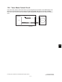
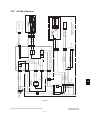
2 - 15
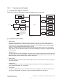
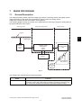
ASIC
PFP
ADU
Thermistors
Fuser unit
Temperature/humidity
sensor
Drum thermistor
Auto-toner sensor
Developer unit
Laser beam sensor
SNS board
Laser diode
LDR board
PFC
DC
(High voltage)
HVPS
Laser optical unit
DC
LVPS
Power supply unit
A/D
converter
D/A
converter
SoC
(System controller)
4 MB
Flash ROM
16
CPU bus (16 bit)
RTC
Battery
SRAM board
SRAM
8
16
8
8
: Option
ASIC
(I/O port)
16
128 kB
64 MB
SDRAM
16 MB
M
32 MB
SDRAM
SDRAM
Scan motor
Driver
16
SDRAM bus (16 bit)
16
AFE
8
USB connector (device)
16
MAIN board
8
Clutches
Bypass unit
Switches
Motors
Copy key card /
Coin controller
PFU
Solenoids
Sensors
I/O
Flash ROM
512 kB
USB connector
(host)
USB connector
(device)
NCU board
TELBOOK board
Download JIG
External keyboard
Control panel
MODEM
Battery
FAX board
Scanner upgrade kit
Network printer kit
LAN connector
(10BASE-T/
100BASE-TX)
2.4.1
CIS
ADF/RADF
2.4
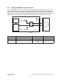
General Description
System block diagram
2
Fig. 2-10
e-STUDIO167/207/237
OUTLINE OF THE MACHINE
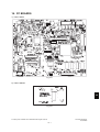
2.4.2
Construction of boards
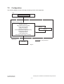
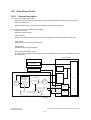
[ 1 ] Construction diagram of boards
This system consists of the following including the MAIN board as a main board.
Scanner unit
Control panel
CIS
HPNL
Toner cartridge
FUS
SRAM
CTIF
Laser optical unit
MAIN
HVPS
AC input
CTRG
PS-ACC
LDR
LVPS
SNS
Main switch
Cover opening/closing
interlock switches
Automatic duplexing unit
: DC power supply line
PFC
: AC power supply line
ADU
: Signal line
Fig. 2-11
[ 2 ] Function of each board
•
MAIN board:
This is the board taking the leading part in all systems. It consists of the SoC, ASIC, memory
(SDRAM, Flash ROM), etc. In the SoC (System control), which is a core of this MAIN board, the
functions of the CPU, image processing, page memory control, CODEC, external interface (USB)
control, etc. are embedded and performed by one chip.
Based on the data input from the control panel, the SoC controls each system, such as the ASIC,
each memory, CIS unit and laser optical unit, and thus permitting the scanning of originals and the
printing of data.
•
SRAM board:
This is the board on which the SRAM for storing the user's setting information and counter value and
its backup function are mounted. When the MAIN board is replaced, attaching this board to the new
MAIN board can assume the data of the previous equipment.
•
HPNL board:
This is the board on which each button switch and LEDs on the control panel, and the LCD control
circuit are mounted.
•
CTRG board:
This is the board on which the IC chip for storing information about the toner cartridge (number of
prints, identification data, etc.) is mounted.
•
CTIF board:
This is the interface board with the CTRG board in the toner cartridge. Information written in the IC
chip on the CTRG board is read into the SoC on the MAIN board through this board.
e-STUDIO167/207/237
OUTLINE OF THE MACHINE
© February 2007 TOSHIBA TEC CORPORATION All rights reserved
2 - 16
•
LDR board:
This is the board on which the laser diode and the ASIC are mounted. The laser is emitted based on
the image data signal output from the SoC on the MAIN board.
•
SNS board:
This is the board on which the light sensor for detecting the radiating position of the laser is
mounted. It outputs the H-sync signal to the SoC on the MAIN board.
•
PS-ACC:
This is the unit to generate each DC (high/low) voltage, which is used in the equipment, from the
external AC electric power input. This is then provided to each electric part.
•
FUS board:
This is the board to provide AC electric power for driving the damp heater.
* Optional for NAD/MJD/CND model, standard for other models.
•
CIS:
This is the unit witch performs optical-to-electrical conversion to convert the light reflected by the
original into the electrical signals. It consists of a light source (LEDs), optical system, CCD sensor,
etc.
•
PFC board:
This is the board to control the optional Automatic Duplexing Unit (ADU) and optional Paper Feed
Pedestal (PFP).
•
ADU board:
This is the board to control the optional Automatic Duplexing Unit (ADU). It detects paper feeding
with a sensor mounted on the ADU board.
© February 2007 TOSHIBA TEC CORPORATION All rights reserved
e-STUDIO167/207/237
OUTLINE OF THE MACHINE
2 - 17
2
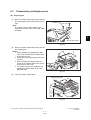
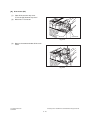
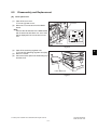
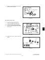
2.5
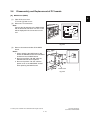
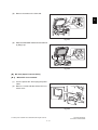
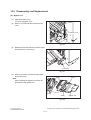
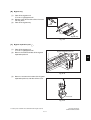
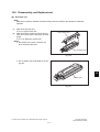
Disassembly and Replacement of Covers
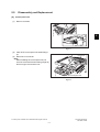
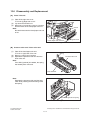
[A] Front cover
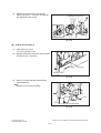
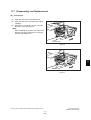
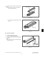
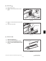
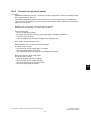
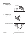
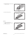
(1)
(2)
(3)
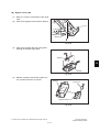
Open the front cover.
Release the upper hinge.
Take off the front cover while lifting it up.
Front cover
Fig. 2-12
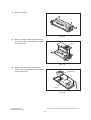
[B] Inner tray
(1)
Remove 2 screws and take off the Inner tray.
Inner tray
Fig. 2-13
e-STUDIO167/207/237
OUTLINE OF THE MACHINE
© February 2007 TOSHIBA TEC CORPORATION All rights reserved
2 - 18
[C] Left cover
(1)
(2)
Take off the Inner tray.
" P.2-18 "[B] Inner tray"
Remove 4 screws and take off the left cover.
2
Left cover
Fig. 2-14
[D] Tray rear cover
(1)
(2)
Take off the left cover.
" P.2-19 "[C] Left cover"
Take off the tray rear cover.
Tray rear cover
Fig. 2-15
© February 2007 TOSHIBA TEC CORPORATION All rights reserved
e-STUDIO167/207/237
OUTLINE OF THE MACHINE
2 - 19
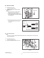
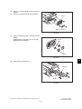
[E] Front right cover
(1)
(2)
(3)
(4)
Take off the front cover.
" P.2-18 "[A] Front cover"
Pull out the toner cartridge.
Open the ADU cover.
Remove 2 screws and take off the front right
cover.
Front right cover
Fig. 2-16
[F] Front upper cover
(1)
Remove 1 screw and take off the front upper
cover.
Front upper cover
Fig. 2-17
e-STUDIO167/207/237
OUTLINE OF THE MACHINE
© February 2007 TOSHIBA TEC CORPORATION All rights reserved
2 - 20
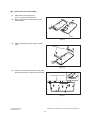
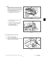
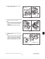
[G] ADU cover
(1)
(2)
(3)
Open the bypass tray.
Open the ADU cover.
Open the transfer unit and release the ADU
stopper on the front side.
(4) Remove 1 screw and take off the ADU stopper on the rear side.
Note:
Be careful not to fall off the ADU cover when
the screws are removed from the ADU stopper.
ADU stopper
ADU stopper
Fig. 2-18
(5)
Take off the ADU cover while sliding it toward
the right.
ADU cover
Fig. 2-19
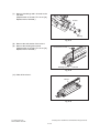
[H] Right front cover
(1)
(2)
(3)
(4)
Take off the front cover.
" P.2-18 "[A] Front cover"
Open the ADU cover.
Pull out the drawer.
Remove 2 screws and take off the right front
cover.
Right front cover
Fig. 2-20
© February 2007 TOSHIBA TEC CORPORATION All rights reserved
e-STUDIO167/207/237
OUTLINE OF THE MACHINE
2 - 21
2
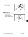
[I]
(1)
(2)
(3)
Right rear cover
Open the ADU cover.
Remove 1 screw and take off the ADU stopper on the rear side.
Take off the 2 screw and take off the right
rear cover.
Right rear cover
Fig. 2-21
[J]
(1)
Rear cover
Remove 5 screws and take off the rear
cover.
Rear cover
Fig. 2-22
e-STUDIO167/207/237
OUTLINE OF THE MACHINE
© February 2007 TOSHIBA TEC CORPORATION All rights reserved
2 - 22
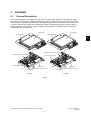
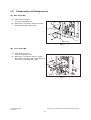
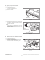
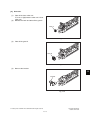
2.6
Disassembly and Replacement of PC boards
[A] MAIN board (MAIN)
2
(1)
Take off the rear cover.
" P.2-22 "[J] Rear cover"
(2) Disconnect 16 connectors.
Note:
Connect the flat harness to the MAIN board
with its electrode side down. An error “CA2”
will be displayed if the connection is incorrect.
Fig. 2-23
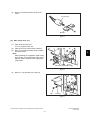
(3)
Remove 6 screws and take off the MAIN
board.
Notes:
1. When replacing the MAIN board, also
attach the SRAM board to the new MAIN
board from the old MAIN board.
2. Be sure to perform “08-389” after the
SRAM board has been replaced.
3. Be sure to perform "05-310" with the
platen cover or the ADF/RADF closed
after replacing the MAIN board.
MAIN board
Fig. 2-24
© February 2007 TOSHIBA TEC CORPORATION All rights reserved
e-STUDIO167/207/237
OUTLINE OF THE MACHINE
2 - 23
[B] SRAM board (SRAM)
(1)
Take off the rear cover.
" P.2-22 "[J] Rear cover"
(2) Release 1 lock support and take off the
SRAM board.
Notes:
1. Be sure to perform “08-388” after the
SRAM board has been replaced.
2. Perform "05-310" with the platen cover
and the ADF/RADF closed after replacing
the SRAM board.
SRAM board
Fig. 2-25
3. Make sure that the direction of the battery
on the SRAM board is correct when
replacing it.
SRAM board
Battery
Fig. 2-26
[C] Fuse PC board (FUS)
Note:
This fuse PC board is copacked with the damp heater unit. (The damp heater unit is optional for
NAD, CND and MJD.)
(1)
(2)
Take off the rear cover.
" P.2-22 "[J] Rear cover"
Remove 2 screws and take off the cover.
Cover
Fig. 2-27
e-STUDIO167/207/237
OUTLINE OF THE MACHINE
© February 2007 TOSHIBA TEC CORPORATION All rights reserved
2 - 24
(3)
Disconnect 2 connectors, remove 1 screw,
and then take off the fuse PC board by lifting
it up.
2
Connector
Fuse PC board
Fig. 2-28
[D] Paper feed controller PC board (PFC)
Note:
This paper feed controller PC board is optional for NAD, CND and MJD.
(1)
Take off the rear cover.
" P.2-22 "[J] Rear cover"
(2) Disconnect 2 connectors, remove 4 screws,
and then take off the paper feed controller
PC board and mylar sheet.
Notes:
• If the ADU (optional) is installed, disconnect 2 connectors of the ADU with other
connectors at the same time before taking off the paper feed controller PC board.
• If the PFP (optional) is installed, disconnect 2 connectors of the PFP with other
connectors at the same time before taking off the paper feed controller PC board.
Connector (ADU)
Mylar
Connector (PFP)
Paper feed controller
PC board
Connector
Fig. 2-29
© February 2007 TOSHIBA TEC CORPORATION All rights reserved
e-STUDIO167/207/237
OUTLINE OF THE MACHINE
2 - 25
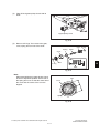
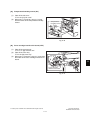
[E] Switching regulator unit (PS)
(1)
Take off the left cover.
" P.2-19 "[C] Left cover"
(2) Disconnect 15 connectors.
Note:
The number of connectors to be disconnected is 15 when the following options are
installed.
A: Paper Feed Controller (GH-1060)
B: Fax Kit (GD-1220)
A
B
Fig. 2-30
Note:
Connect the connectors to the correct faston
terminals on the switching regulator board.
Connector
Harness
F. Red
Black-thick
E. Blue
White-thick
D. White
Black-thin
C. White
Red-thin
B. White
Red-thick
A. White
White-thick
F
E
D
C
B
A
Fig. 2-31
(3)
Remove 2 screws, slide the switching regulator unit with the whole case slightly to the
front, and then lift it up to take it off.
Switching regulator unit
Fig. 2-32
e-STUDIO167/207/237
OUTLINE OF THE MACHINE
© February 2007 TOSHIBA TEC CORPORATION All rights reserved
2 - 26
(4)
(5)
Disconnect 7 connectors.
Remove 1 screw and 1 ground wire.
Connector
Connector
2
Fig. 2-33
Note:
Make sure that the position is correct when
inserting the connector.
Green/Yellow
Black
White
White Gray
2
1
4
3
Black Brown
Fig. 2-34
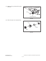
(6)
Remove 8 screws, release 1 locking support,
and take off the switching regulator board.
Locking support
Switching regulator board
Fig. 2-35
© February 2007 TOSHIBA TEC CORPORATION All rights reserved
e-STUDIO167/207/237
OUTLINE OF THE MACHINE
2 - 27
[F] Switching regulator cooling fan (M6)
(1)
(2)
Take off the left cover.
" P.2-19 "[C] Left cover"
Disconnect 1 connector and take off the
switching regulator cooling fan while sliding it
upward.
Switching regulator cooling fan
Connector
Fig. 2-36
e-STUDIO167/207/237
OUTLINE OF THE MACHINE
© February 2007 TOSHIBA TEC CORPORATION All rights reserved
2 - 28
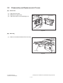
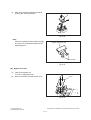
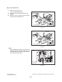
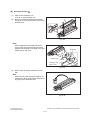
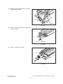
2.7
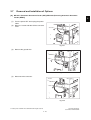
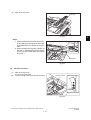
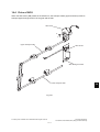
Removal and Installation of Options
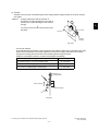
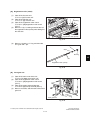
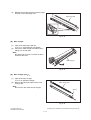
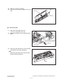
[A] MR-2017 (Automatic Document Feeder (ADF))/MR-3019 (Reversing Automatic Document
Feeder (RADF))
(1)
(2)
Turn the power OFF and unplug the power
cable.
Remove 1 screw and take off the connector
cover.
Fig. 2-37
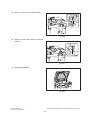
(3)
Remove the ground wire.
Fig. 2-38
(4)
Disconnect the connector.
Fig. 2-39
© February 2007 TOSHIBA TEC CORPORATION All rights reserved
e-STUDIO167/207/237
OUTLINE OF THE MACHINE
2 - 29
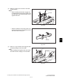
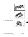
2
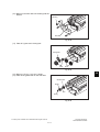
(5)
Remove 1 screw on the rear right side.
Fig. 2-40
(6)
Remove 1 screw and 1 washer on the rear
left side.
Fig. 2-41
(7)
Open the ADF/RADF.
Fig. 2-42
e-STUDIO167/207/237
OUTLINE OF THE MACHINE
© February 2007 TOSHIBA TEC CORPORATION All rights reserved
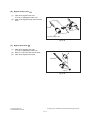
2 - 30
(8)
Remove 2 screws on the front side.
2
Fig. 2-43
(9)
Slide the ADF/RADF backward and take off
by lifting it up.
Fig. 2-44
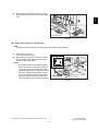
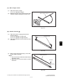
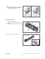
[B] MY-1027 (Paper Feed Unit (PFU))
[B-1]
(1)
(2)
When PFP is not installed
Turn the power OFF and unplug the power
cable.
Remove 1 screw and take off the PFU connector cover.
Fig. 2-45
© February 2007 TOSHIBA TEC CORPORATION All rights reserved
e-STUDIO167/207/237
OUTLINE OF THE MACHINE
2 - 31
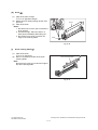
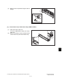
(3)
Remove the ground wire.
Fig. 2-46
(4)
Disconnect the connector.
Fig. 2-47
(5)
Install the PFU connector cover.
Fig. 2-48
e-STUDIO167/207/237
OUTLINE OF THE MACHINE
© February 2007 TOSHIBA TEC CORPORATION All rights reserved
2 - 32
(6)
(7)
Take off the rear cover.
" P.2-22 "[J] Rear cover"
Disconnect 1 connector (optional damp
heater). Release the harness from the harness clamp.
2
Fig. 2-49
(8)
Take off the drawer of the equipment and
PFU drawer.
Fig. 2-50
(9)
Remove 1 screw and take off 1 fixing bracket
on the front left side.
Fig. 2-51
© February 2007 TOSHIBA TEC CORPORATION All rights reserved
e-STUDIO167/207/237
OUTLINE OF THE MACHINE
2 - 33
(10) Remove 1 screw and take off 1 fixing bracket
on the front right side.
Fig. 2-52
(11) Remove 1 screw and take off 1 fixing bracket
on the rear left side.
Fig. 2-53
(12) Remove 1 screw and take off 1 fixing bracket
on the rear right side.
Fig. 2-54
e-STUDIO167/207/237
OUTLINE OF THE MACHINE
© February 2007 TOSHIBA TEC CORPORATION All rights reserved
2 - 34
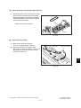
(13) Lift up the equipment and take off the PFU.
2
Fig. 2-55
[B-2]
(1)
(2)
When PFP is installed
Take off the rear cover.
" P.2-22 "[J] Rear cover"
Remove 1 ground wire and 2 connectors.
Fig. 2-56
(3)
(4)
Take off the equipment from the PFU.
" P.2-31 "[B-1] When PFP is not installed"
Take off the PFP drawer.
Fig. 2-57
© February 2007 TOSHIBA TEC CORPORATION All rights reserved
e-STUDIO167/207/237
OUTLINE OF THE MACHINE
2 - 35
(5)
Remove 1 screw and take off 1 fixing bracket
on the front left side.
Fig. 2-58
(6)
Remove 1 screw and take off 1 fixing bracket
on the front right side.
Fig. 2-59
(7)
Remove 1 screw and take off 1 fixing bracket
on the rear left side.
Fig. 2-60
e-STUDIO167/207/237
OUTLINE OF THE MACHINE
© February 2007 TOSHIBA TEC CORPORATION All rights reserved
2 - 36
(8)
Remove 1 screw and take off 1 fixing bracket
on the rear right side.
2
Fig. 2-61
(9)
Take off the PFU while lifting it up.
Fig. 2-62
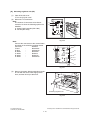
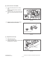
[C] KD-1022 (Paper Feed Pedestal (PFP))
(1)
Take off the equipment and the PFU. Then
take off the PFP.
" P.2-35 "[B-2] When PFP is installed"
Fig. 2-63
© February 2007 TOSHIBA TEC CORPORATION All rights reserved
e-STUDIO167/207/237
OUTLINE OF THE MACHINE
2 - 37
e-STUDIO167/207/237
OUTLINE OF THE MACHINE
© February 2007 TOSHIBA TEC CORPORATION All rights reserved
2 - 38
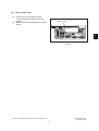
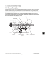
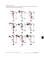
3.
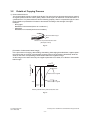
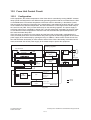
3.1
COPY PROCESS
General Description of Copying Process
Paper exit
(8)
(10)
(2) Data reading(scanning)
CIS
600 dpi,7084 pixel
Image processing
(3)
(9)
Discharging
Discharge LED (red)
Wavelength 660nm x10pcs
(1)
Cleaning
Blade method
Charging
(7)
e-STUDIO167/207:-448V
e-STUDIO237
:-454V
(grid voltage)
Separation
H -107 µADC
C -107 µADC
L
-70 µADC
Data writing
Semiconductive laser
Pw=4.0 nJ/mm 2
(6)
Transfer
H
C
L
(4)
3
Fusing
Lamp heating method
564W x2
Development
Magnetic roller
Bias -340VDC+AC
(5)
Toner
Carrier
340 µADC
369 µADC
282 µADC
Transfer bias
DC
+565V
Bypass feeding
(100 sheets)
Drawer feeding
(250 sheets)
PFU
(250 sheets)
Fig. 3-1
(1)
(2)
(3)
(4)
(5)
(6)
Charging: Applies negative charge on the
surface of the photoconductive drum.
#
Data reading: The images on the original
are converted into electrical signals.
#
Data writing: The electrical signals are converted into light signal (laser emission)
which exposes the surface of the photoconductive drum.
#
Development: Negatively-charged toner
adheres to the photoconductive drum and
forms visible image.
#
Transfer bias: Improves transfer efficiency.
#
Transfer: Transfers the visible toner image
on the photoconductive drum onto paper.
#
(7)
(8)
(9)
(10)
© February 2007 TOSHIBA TEC CORPORATION All rights reserved
Separation: Separates paper with the toner
image from the photoconductive drum.
#
Fusing: Fuses the toner image onto the
paper by applying heat and pressure.
#
Cleaning: Scrapes off the residual toner
from the drum.
#
Discharging: Eliminates the residual negative charge from the surface of the photoconductive drum.
e-STUDIO167/207/237
COPY PROCESS
3-1
3.2
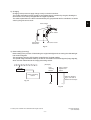
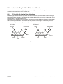
Details of Copying Process
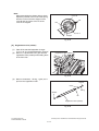
1) Photoconductive drum
The photoconductive drum consists of two layers.The outer layer is a photoconductive layer made of
an organic photoconductive carrier (OPC), and the inner layer is an aluminum conductive base in a
cylindrical form. The photoconductor has the following property: when it is exposed to light, the electrical resistance it possesses increases or decreases according to the strength of the light.
Example:
- Strong light
Resistance is decreased (works as a conductor.)
- Weak light
Resistance is increased (works as an insulator.)
Photoconductive layer
Base
Structure of the photoconductive drum
(Example of OPC)
Fig. 3-2
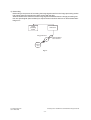
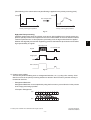
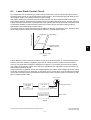
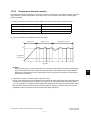
[Formation of electrostatic latent image]
In the processes of charging, data reading, data writing, discharging described later, negative potential of the areas on the drum corresponding to black areas of the original are eliminated, while the
areas on the drum corresponding to white areas retains the negative charge.
As this image on the drum formed by the negative potential is not visible, it is called an “electrostatic
latent image.”
Surface potential (V)
Time (t)
0
Black area of original
-500
White area of original
Discharge Charging
process
process
Electric potential of the photoconductive drum
Fig. 3-3
e-STUDIO167/207/237
COPY PROCESS
© February 2007 TOSHIBA TEC CORPORATION All rights reserved
3-2
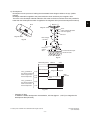
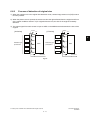
2) Charging
Charging is the process to apply charge evenly on the drum surface.
The needle electrode produces negative corona discharge is controlled by the grid, allowing the
drum surface to be evenly charged with the negative potential.
The surface potential on the drum is determined by the grid potential and is controlled to a certain
value by the grid control circuit.
3
Main charger
Drum rotation
High-voltage
transformer
Grid control circuit
Fig. 3-4
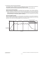
3) Data reading (scanning)
Data reading is the process of illuminating the original with light and converting the reflected light
into electrical signals.
This equipment uses the CIS (Contact Image Sensor) for data reading.
The optical image information read by the CIS is converted into electrical signals (image signals),
which are then transmitted to the image processing section.
(Example)
Light
receiving
amount
CIS
Light
Value of image
signals to be
output
255
Image processing
section
Difference between
"light " and "dark" is
divided into 256 steps.
Fig. 3-5
Dark
0
Fig. 3-6
© February 2007 TOSHIBA TEC CORPORATION All rights reserved
e-STUDIO167/207/237
COPY PROCESS
3-3
4) Data writing
Data writing is the process of converting the image signals sent from the image processing section
into optical signal and exposing the drum surface with the light.
Semiconductive laser element converts image signals transmitted from the image processing section into optical signal (laser emission) to expose the drum surface and form an electrostatic latent
image on it.
Image
processing
section
LDR board
Polygonal mirror
Semiconductive
laser element
Photoconductive
drum
Fig. 3-7
e-STUDIO167/207/237
COPY PROCESS
© February 2007 TOSHIBA TEC CORPORATION All rights reserved
3-4
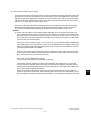
5) Development
Development is the process of making the electrostatic latent images visible to the eye (visible
images).
Developer material is supplied to the photoconductive drum surface by the magnetic roller.
The toner in the developer material adheres to the areas on the drum surface where the potential is
lower than the developer bias which is applied to the magnetic roller (reverse development method).
3
Magnet
Drum
Magnetic roller
Toner
Carrier (always attracted
onto the magnet)
Toner
Magnetic roller
Bias voltage
- 357 VDC
Fig. 3-8
Toner
Photoconductive
drum
Photoconductive layer
Aluminum base
Fig. 3-9
White background
Halftone
Solid
White background
Image not developed
The (-) potential of
- 440V
the photoconductive
drum is higher than
the developer bias. - 340V
Image developed by
toner
- 300V
Bias
potential
The (-) potential of
- 200V
the photoconductive
drum is lower than
the developer bias. - 100V
0
Fig. 3-10
-
Charging AC bias
To obtain the stable development characteristics, AC bias (approx. 1,100 V) is charged to the
development bias (DC bias).
© February 2007 TOSHIBA TEC CORPORATION All rights reserved
e-STUDIO167/207/237
COPY PROCESS
3-5
-
Developer material
The developer material consists of a mixture of the toner and carrier. The toner is charged to the
negative polarity and the carrier to positive polarity due to the friction with each other caused by
mixing.
Toner:
Carrier:
Mainly consists of the resin and carbon.
Consists of the ferrite and resin coating on
its surface to provide consistent frictional
electrification.
Carbon
(5-10%)
5-20 µm
Ferrite
Resin (90-95%)
[Toner]
30-100 µm
[Carrier]
Fig. 3-11
Note:
If the developer material is used for a long time (beyond its normal
life span), the toner is caked onto the carrier.
#
The charging performance of the carrier is lowered.
Symptom:
1. Image density is lowered.
2. Toner scattering occurs.
3. Background fogging occurs.
Solution:
Replace the developer material.
Toner
Carrier
No frictional electrification
occurs on the area where the
toner is caked.
Fig. 3-12
e-STUDIO167/207/237
COPY PROCESS
© February 2007 TOSHIBA TEC CORPORATION All rights reserved
3-6
-
Magnetic roller
Magnetic brush development
The south and north poles are arranged inside the magnetic roller as shown in the right figure.
The developer material forms a brush-like fluff which contacts the photoconductive drum surface.
#
This is caused by the magnetic force lines between the south and north poles.
3
Photoconductive
drum
N
S
S
Magnetic roller
Magnetic force
line
Fig. 3-13
© February 2007 TOSHIBA TEC CORPORATION All rights reserved
e-STUDIO167/207/237
COPY PROCESS
3-7
-
Additional Explanation
The life of the toner cartridge (number of output pages) varies depending on the following conditions.
Coverage of originals (printing image ratio of the original size) and density of original background
Size and density of originals
The existence of solid black when making prints (when a book is copied and the original cover is
partially opened)
Temperature and humidity in the room when making prints.
Prints density and image quality mode
As indicated in the figure below, the life of the toner cartridge varies depending on the copy mode
and coverage of originals.
Is this graph, the toner consumption for copying in TEXT/PHOTO mode using chart “A” is defined
as 100%.
Output pages
140%
24,000 or
5,900 pages
100%
80%
43%
A
36%
B
C
A
TEXT/PHOTO
A
TEXT
PHOTO
Type of originals
A
B
C
Fig. 3-14
e-STUDIO167/207/237
COPY PROCESS
© February 2007 TOSHIBA TEC CORPORATION All rights reserved
3-8
6) Transfer
Transfer is the process of transferring the toner image (visible image) formed on the drum surface
onto paper.
Method:
A paper passing the side of the drum is
charged to the opposite polarity to the that of
toner by the corona discharge of the transfer
charger.
#
The toner moves from the drum surface onto
the paper.
3
Paper
Drum
Transfer
charger
Fig. 3-15
-
For smooth transfer
In the transfer bias processing of this equipment, bias voltage (+565 VDC) is applied to the registration roller and transfer unit transport guide to prevent the charge produced by the transfer
charger from flowing into the transfer unit transport guide through the paper.
Output is controlled as follows to realizes the desirable transfability.
Paper position against transfer point
Transfer output
From leading edge to 11 mm from leading edge
(H) 340 µADC
From 11 mm from leading edge to 5 mm from trailing edge
(C) 369 µADC
From 5 mm from trailing edge to trailing edge
(L) 282 µADC
Direction of
transportation
Drum rotation
Transfer charger
Toner
Fig. 3-16
© February 2007 TOSHIBA TEC CORPORATION All rights reserved
e-STUDIO167/207/237
COPY PROCESS
3-9
7) Separation
Separation is the process of separating paper which is temporarily adhering to the drum due to the
static electricity during the transfer process.
Method:
Apply negative DC bias to the separation
charger.
#
The positive charge on the paper is decreased.
#
The electrostatic adherence force between the
paper and drum becomes weak.
#
The paper is separated from the drum by its
own stiffness.
Drum
rotation
Separation charger
Direction of
transportation
Fig. 3-17
-
Output is controlled as follows to realizes the desirable separability.
Paper position against transfer point
Separation output
From leading edge to 11mm from leading edge
(H) -107 µADC
From 11mm from leading edge to 46mm from leading edge
(L) -70 µADC
From 46mm from leading edge to 48mm from trailing edge
(C) -107 µADC
From 48mm from trailing edge to trailing edge
(L) -70 µADC
Paper may not be separated from the drum surface because of moisture or malfunction of the
transfer/separation charger during printing. As the result, the paper enters into the cleaner and
causes jamming. To prevent this, a separation finger is used to forcibly separate the paper which
was left around the drum.
Separation finger
Paper
movement
Separation
charger
Drum rotation
Fig. 3-18
e-STUDIO167/207/237
COPY PROCESS
© February 2007 TOSHIBA TEC CORPORATION All rights reserved
3 - 10
8) Fusing
Fusing is the process of melting the toner on the paper and fixing it firmly on the paper.
Method:
The melting point of the toner (main ingredient: resin) is 90-100°C.
#
(Heat)
Toner is melted by the heat of the surface of
the fuser roller.
+
(Pressure) The pressure roller is pressed against the
fuser roller by the springs to increase the
adherence of the melted toner onto the
paper.
#
Heat and pressure are applied to the paper
when it passes between the fuser roller and
pressure roller.
#
(Fusing)
The toner is fused on the paper.
Pressure
Fuser roller
Paper
Fig. 3-19
Separation finger
Fuser roller
(Pressure)
Heater lamp
Pressure roller
Paper
movement
Fig. 3-20
9) Cleaning
Cleaning is the process of removing the residual toner from the photoconductive drum.
The edge of the urethane rubber cleaning blade is pressed against the photoconductive drum surface to scrape off the residual toner on it. The toner is then caught by the recovery blade.
Recovery blade
Cleaning blade
Drum rotation
Fig. 3-21
© February 2007 TOSHIBA TEC CORPORATION All rights reserved
e-STUDIO167/207/237
COPY PROCESS
3 - 11
3
10)Discharging
Discharging is the process of eliminating the negative charge remaining on the photoconductive
drum before the next charging process.
If the residual charge is not eliminated, the following phenomenon occurs:
Negative charge remaining on the photoconductive drum surface causes ungiven application of
the charge for the next printing.
#
Discharge LED
Photoconductive
drum
The next print will have a double image. (The
preceding image appears.)
#
Solution:
The entire surface of the photoconductive drum
is illuminated with light by the discharge LED
array.
#
Ground
Fig. 3-22
The photoconductive drum becomes electrically conductive.
#
All of the negative charge remaining on the photoconductive drum is conducted to the ground.
#
Preparation for the next printing is completed.
e-STUDIO167/207/237
COPY PROCESS
© February 2007 TOSHIBA TEC CORPORATION All rights reserved
3 - 12
3.3
Comparison with e-STUDIO230/280
Process
e-STUDIO230/280
e-STUDIO167/207/237
1. Photoconductive drum
• Sensitivity
• Surface potential
OD-1600 (OPC ø30)
Highly sensitized/durable drum
-475 V
$
$
-440 V
2. Charging
• Grid voltage
Scorotron method
-495 V
$
-448 V (e-STUDIO167/207)
-454 V (e-STUDIO237)
Semiconductor laser
(Adjustment not required)
4.0 nJ/mm2
$
One magnetic roller
Magnetic bridge-circuit method
Toner cartridge
Density detection method
T-2320, T-2320E, T-2320D, T-2320C,
T-2320T
D-2320, D-2320C
DC-357 V Adjustable output
(during printing)
AC 1100 V (Adjustment not required,
during printing)
DC+150 V Fixed (others)
$
$
$
$
T-1640, T-1640E, T-1640D
T-1640C, T-1640T
$
DC -340 V Adjustment output (during
printing)
AC 1100 V (Adjustment not required,
during printing)
No DC+ (positive) output
5. Transfer
• Transfer bias
Adjustable output (Constant current)
+600 V (Adjustment not required)
$
+565 V (Adjustment not required)
6. Separation
Adjustable output
(Constant current)
$
Exposure after cleaning
Red LED
$
$
Cleaning blade
Reuse (There is the recovered toner
supply mechanism.)
$
$
Long-life fuser roller method
Fuser roller:
Thin roller coated with fluoroplastic
(ø30)
Pressure roller:
PFA tube roller (ø30)
Cleaning roller for pressure roller (ø16)
Heater lamp
Turned ON/OFF by thermistor
$
$
3. Data writing
• Light source
•
Light amount
4. Development
• Magnetic roller
• Auto-toner
• Toner supply
• Toner-empty detection
• Toner
•
•
Developer material
Developer bias
7. Discharge
• Discharging position
• Discharge LED
8. Cleaning
• Method
• Recovered toner
9. Fusing
• Method
•
•
Cleaning
Heater
© February 2007 TOSHIBA TEC CORPORATION All rights reserved
Pressure roller:
PFA tube roller (ø25)
None
$
e-STUDIO167/207/237
COPY PROCESS
3 - 13
3
e-STUDIO167/207/237
COPY PROCESS
© February 2007 TOSHIBA TEC CORPORATION All rights reserved
3 - 14
4.
GENERAL OPERATION
4.1
Overview of Operation
Operation of equipment
Operation during initializing, pre-running and ready
Drawer feed copying by [START] button
Bypass feed copying
Copying operation
Interrupt copying
© February 2007 TOSHIBA TEC CORPORATION All rights reserved
4
e-STUDIO167/207/237
GENERAL OPERATION
4-1
4.2
4.2.1
Description of Operation
Warming-up
1) Initialization
Power ON
Heater lamp ON
“Please wait” is displayed
Fan motors ON
Initialization of scanning system
- The CIS unit moves to the home position.
- The CIS unit moves to the peak detection position.
- The LED of CIS is turned ON.
- Peak detection (white color is detected by the shading correction plate)
- The LED of CIS is turned OFF.
- The CIS unit moves to the home position.
“READY (WARMING UP)” is displayed
2) Pre-running operation (Only when the temperature is at 16 °C or less)
The pre-running operation is started when the temperature of the fuser roller surface reaches a certain temperature.
!The main motor is turned ON
- Fuser roller rotated.
- Drum rotated.
!Pre-running operation stops after 15 seconds
3) When the surface temperature of the fuser roller becomes sufficient for fusing,
“READY” is displayed
4.2.2
Ready state (ready for copying)
Buttons on the control panel enabled
!When no button is pressed for a certain period of time,
- Set number “1” is displayed. Equipment returns to the normal ready state.
e-STUDIO167/207/237
GENERAL OPERATION
© February 2007 TOSHIBA TEC CORPORATION All rights reserved
4-2
4.2.3
Drawer feed copying
1) Press the [START] button
!“READY” Æ “COPYING”
!CIS LED ON
!Scan motor ON
CIS unit move forward
!Polygonal motor rotates in high speed
!Main motor and exit motor ON
- The drum, fuser unit, developer unit and exit roller are driven.
2) Drawer paper feeding
!Main charger, developer bias and discharge LED ON. Fans are rotated in high speed. Pickup
solenoid ON.
- Pickup roller start to rotate.
!Pickup solenoid OFF after a certain period of time
!Paper reaches the registration roller
- The registration sensor is turned ON and aligning is performed.
3) After the scanning operation:
!Registration clutch ON after a certain period of time % paper is transported to the transfer area
!Copy counter operates
4) After the registration clutch is turned ON:
!Transfer charger ON after a certain period of time
!Copy counter operates
5) Completion of scanning
!Scan motor OFF
!CIS LED OFF
!Registration clutch OFF (after the trailing edge of the paper passed the registration roller)
!Ready state
6) Paper exit
!Exit sensor detects the trailing edge of the paper
!Main charger, developer bias and discharge LED OFF
!Polygonal motor, main motor and exit motor OFF
!Drum, fuser unit and developer unit stop
!Fans return to the ready rotation
!“READY” is displayed and the equipment enters the ready state
7) Timing chart for copying one A4 size sheet fed from the drawer
(Unit : ms)
Main motor
Registration sensor
Registration clutch
MVDEN signal
9400
0
2354
4829
2594
5009
2801
5103
Exit sensor
4615
© February 2007 TOSHIBA TEC CORPORATION All rights reserved
6921
e-STUDIO167/207/237
GENERAL OPERATION
4-3
4
4.2.4
Bypass feed copying
1) Insert a sheet of paper into the bypass tray.
!Bypass paper sensor ON
- Bypass feed priority state.
2) Press the [START] button
!“READY” Æ “COPYING”
!CIS LED ON
!Scan motor ON
CIS unit move forward
!Polygonal motor rotates in high speed
!Main motor and exit motor ON
- The drum, fuser unit, developer unit and exit roller are driven.
3) Bypass feeding
!Main charger, developer bias and discharge LED ON. Fans are rotated in high speed.
!Bypass pickup solenoid ON
- The bypass pickup roller start to rotate.
- The bypass pickup roller is lowered.
- The bypass feed roller start to rotate.
!Paper reaches the registration roller
!Aligning operation
!After a certain period of time, the bypass pickup solenoid OFF
4) Hereafter, the operation 3) through 6) of " P.4-3 "4.2.3 Drawer feed copying" is repeated.
4.2.5
Interruption copying
1) Press the [INTERRUPT] button
!LED “INTERRUPT” ON
!Copying operation in progress is temporarily stopped. CIS unit return to appropriate positions
!“Job interrupted” is displayed
!Automatic density and reproduction ratio 100% are set (The set number remains the same)
2) Select the desired copy condition
3) After the interruption copying is finished:
!LED “INTERRUPT” OFF by pressing the [INTERRUPT] button
!“READY to resume job” is displayed
4) Press the [START] button
!The copying operation before the interruption is resumed
e-STUDIO167/207/237
GENERAL OPERATION
© February 2007 TOSHIBA TEC CORPORATION All rights reserved
4-4
4.3
Detection of Abnormality
When something abnormal has occurred in the equipment, the symbols corresponding to the type of
abnormality are displayed.
4.3.1
Types of abnormality
1) Abnormality cleared without turning OFF the door switch
(A) Add paper
(B) Pick-up failure in bypass
4
2) Abnormality not cleared without turning OFF the door switch
(C) Misfeed in equipment
(D) Replace the toner cartridge
(E) Developer unit not installed properly
3) Abnormality not cleared without turning OFF the main switch
(F) Call for service
© February 2007 TOSHIBA TEC CORPORATION All rights reserved
e-STUDIO167/207/237
GENERAL OPERATION
4-5
4.3.2
Description of abnormality
(A) Add paper
[In cases of the equipment drawer or the PFU / PFP drawer ] (When drawer is not installed)
•
Drawer empty sensor detects the presence or absence of paper.
No drawer detected
#
“Add paper” is displayed
The LED on the control panel corresponding to the drawer blinks (When the drawer is selected)
#
[START] button disabled
[In cases of the equipment drawer or the PFU drawer] (When the drawer is installed)
Drawer detected
#
Paper empty sensor OFF
#
“Add paper” is displayed
The LED on the control panel corresponding to the drawer blinks (When the drawer is selected)
#
[START] button disabled
[In case of the PFP drawer] (When the drawer is installed)
•
When the power is turned ON or the drawer is installed
PFP starts initialization
#
The detection of paper existence starts
Tray-up motor ON – Tray is raised
At this time, the tray-up sensor and paper empty sensor are OFF
% When the tray-up sensor is not turned ON in a fixed period of time
Tray abnormality % “Add paper” is displayed regardless of the existence of paper
% Cleared by turning the power ON and then OFF
% The tray-up sensor is turned ON in a fixed period of time
- The tray-up motor is stopped.
At this time, if the paper empty sensor is
ON: It is judged that there is paper
OFF: It is judged that there is no paper
#
The lamp on the control panel corresponding to the drawer blinks (When
the drawer is selected)
e-STUDIO167/207/237
GENERAL OPERATION
© February 2007 TOSHIBA TEC CORPORATION All rights reserved
4-6
•
When paper becomes almost empty as they fed out during copying,
% The tray-up sensor is turned OFF.
% The tray-up motor is turned ON – the tray is raised.
% The tray-up sensor is turned ON.
% The tray-up motor is stopped.
•
When the paper empty sensor is turned OFF even if the tray-up sensor is ON during copying,
#
The sensor is detecting that no paper exists.
#
The lamp on the control panel corresponding to the drawer blinks (When the drawer is
selected)
#
Copying is stopped
(B) Pick-up failure in bypass
•
During bypass feeding
Bypass pickup solenoid ON
#
Registration sensor is not turned ON in a fixed period of time
#
“Misfeed in bypass“ is displayed : E12
#
Copying operation is disabled
#
Solution: The bypass paper sensor is turned OFF by removing the paper from the bypass tray.
© February 2007 TOSHIBA TEC CORPORATION All rights reserved
e-STUDIO167/207/237
GENERAL OPERATION
4-7
4
(C) Misfeed in equipment
•
Exit sensor detects jamming of the leading edge of paper.
#
Registration clutch ON
ON
#
Less than 1.808 sec.
Registration clutch
Exit sensor ON
If the exit sensor is not turned ON after 1.808
sec.
ON
Exit sensor
Timer
#
0
1.808sec.
Paper jam (E01)!% The copying operation is
stopped.
Paper jam (E01)
Fig. 4-1
•
Exit sensor detects jamming of the tailing edge of paper.
#
Registration clutch OFF
#
Registration clutch
OFF
Less than 1.759 sec.
Exit sensor OFF
If the exit sensor is not turned OFF after 1.759
sec.
Exit sensor
ON
Timer
#
0
Paper jam (E02)!% The copying operation is
stopped.
1.759sec.
Paper jam (E02)
Fig. 4-2
•
Immediately after the power ON
#
Any of all sensors on paper transport path detects paper (ON)
#
Paper jam (E03)
•
Front cover is opened during copying
#
Paper jam (E41)
•
The registration sensor (S4) is not turned ON in a fixed period of time when paper is fed out of the
ADU.
#
Paper jam (E11)
e-STUDIO167/207/237
GENERAL OPERATION
© February 2007 TOSHIBA TEC CORPORATION All rights reserved
4-8
•
The ADU sensor (on the ADU board) does not detect paper in a fixed period of time when the
paper is transported within the ADU.
#
Paper jam (E51)
•
Registration sensor detects jamming of the leading edge of paper:
Registration sensor is not turned ON in a fixed period of time after the feeding starts.
#
4
Paper jam (E12, E13, E21, E30 and E33)
(The error code differs depending on the paper source. Refer to the error code table in Service
Handbook.)
•
The PFU paper feed sensor is not turned ON in a fixed period of time after the pickup solenoid is
turned ON.
#
Paper jam (E14)
•
The PFP upper drawer feed sensor is not turned ON in a fixed period of time after the paper feed
clutch is turned ON when paper is fed out of the PFP.
#
Paper jam (E15 and E36)
•
The PFP lower drawer feed sensor is not turned ON in a fixed period of time after the paper feed
clutch is turned ON when paper is fed out of the PFP.
#
Paper jam (E16)
•
The PFU feed sensor is not turned ON in a fixed period of time after the paper feed clutch is turned
ON when paper is fed out of the PFP.
#
Paper jam (E32 and E35)
(The error code differs depending on its paper source. Refer to the error code list in the Service
Handbook.)
(D) Replace the toner cartridge
•
Toner density becomes low
#
Auto-toner sensor detects the absence of the toner
#
Control circuit % The toner lamp brinks: the copying operation disabled
Solution: Open the front cover and replace the toner cartridge with a new one.
Toner is supplied % copying operation enabled.
© February 2007 TOSHIBA TEC CORPORATION All rights reserved
e-STUDIO167/207/237
GENERAL OPERATION
4-9
(E) Developer unit not installed properly
•
Disconnection of the connectors of the developer unit
#
“Set process unit” is displayed.
[START] button disabled.
#
Solution: Connect the connectors of the developer unit and close the front cover.
(F) Call for service
Error code is displayed instead of the set number by pressing the [CLEAR] button and [8] button
simultaneously when the service call lamp is blinking.
Refer to the error code table in the Service Handbook.
e-STUDIO167/207/237
GENERAL OPERATION
© February 2007 TOSHIBA TEC CORPORATION All rights reserved
4 - 10
4.4
4.4.1
Flow Chart
Immediately after the power is turned ON
Main switch ON
4
DC power ON
Restart
YES
Cover is open?
Heater lamp ON
YES
Registration sensor
ON?
Scan motor ON
NO
YES
Home position
detected?
Exit sensor ON?
NO
YES
YES
ADU sensor ON?
NO
Peak detected?
YES
NO
Paper jam
"E03"
A
B
Call for service
"C26"
13 - 15 seconds
elapsed?
NO
YES
Call for service
"C21"
Fig. 4-3
© February 2007 TOSHIBA TEC CORPORATION All rights reserved
e-STUDIO167/207/237
GENERAL OPERATION
4 - 11
A
Temperature of
the fuser roller ready
for pre-running?
NO
YES
Thermistor
broken?
NO
Heater lamp
broken?
YES
Fuser roller
reached ready
temp.?
NO
YES
NO
Polygonal
motor in abnormal
condition?
NO
YES
Call for service
Call for service
Call for service
“C41”
“C43”
“C44”
“CA1”
YES
B
READY
Fig. 4-4
e-STUDIO167/207/237
GENERAL OPERATION
© February 2007 TOSHIBA TEC CORPORATION All rights reserved
4 - 12
4.4.2
Automatic paper feed copying
Press [START] button
Developer bias ON
Main chargeON
Discharge LED ON
Main motor ON
Polygonal motor ON
Exit motor ON
4
Transport system
control
Processing system
control
Polygonal motor
normal rotation?
YES
Scanning system
control
NO
Call for service
“CA1”
Laser ON
Pickup solenoid ON
CIS move forward
Transfer charger ON
Pickup solenoid OFF
CIS move backward
CIS stopped
Registration clutch ON
Counter ON/OFF
Transfer charger OFF
NO
Registration clutch OFF
H-Sync
OK?
Call for
service
“CA2”
NO
CIS ON
CIS OFF
YES
NO
Remaining set
number=0?
Remaining set
number=0?
YES
Laser OFF
YES
Exit sensor
detected leading
edge of paper?
Scanning system
control completed
NG
OK
Paper jam
Processing system
control completed
C
“E01”
Fig. 4-5
© February 2007 TOSHIBA TEC CORPORATION All rights reserved
e-STUDIO167/207/237
GENERAL OPERATION
4 - 13
C
Paper jam
NG
“E02”
Exit sensor
detected trailing
edge of paper?
OK
Polygonal motor OFF
Main charger OFF
Discharge LED OFF
Developer bias OFF
Exit motor OFF
Drum rotation reversed
Main motor OFF
READY
Fig. 4-6
e-STUDIO167/207/237
GENERAL OPERATION
© February 2007 TOSHIBA TEC CORPORATION All rights reserved
4 - 14
5.
5.1
CONTROL PANEL
General Description
The control panel consists of button switches to operate the equipment and select various modes, and
LEDs and an LCD to display codes, values and the states (including each mode) of the equipment. The
button switches, the LEDs and an LCD are mounted on the control panel PC board (HPNL) and are
installed the inside of the control panel.
When the operator’s attention is required, graphic symbols appear with messages explaining the condition of the equipment in the LCD panel.
5
Fig. 5-1
© February 2007 TOSHIBA TEC CORPORATION All rights reserved
e-STUDIO167/207/237
CONTROL PANEL
5-1
5.2
5.2.1
Items Shown on the Display Panel
Display
1) Basic display
Displays buttons and messages.
READY
100%
ZOOM
1
NONSORT
FINISHING
EDIT
Fig. 5-2
2) Paper jam display
Displays error code, paper jam position and paper jam release guidance.
Misfeed in copier E41
Open side cover
of the copier.
1/ 6
Fig. 5-3
3) Service call display
Displays error code and service call symbol.
Call for service
C01
Fig. 5-4
4) When input values can be changed by the up or down button in the self-diagnosis mode, the LED in
the center of the up, down, left and right buttons is lit.
e-STUDIO167/207/237
CONTROL PANEL
© February 2007 TOSHIBA TEC CORPORATION All rights reserved
5-2
5.2.2
Message
No.
Message
1
Wait warming up
2
READY
3
COPYING
4
Saving energy
5
6
Select original size
-
7
Cassette * empty
8
Toner empty
9
Misfeed in bypass
10
Misfeed in copier
(Copier machine)
Misfeed in doc. Feeder
(ADF)
11
12
Condition of machine
Being warmed up
• Displayed after the main switch is
turned ON up until the machine
becomes ready for copying
•
Standby for copying
• The machine is ready for copying
and operator's instructions on copying conditions can be input
•
• Returns to the default condition if
no key is pressed for the setting
time of auto clear timer
•
Now copying
•
• Displayed by pressing the START
key
• Copy quantity indicator becomes
"ex. 3 2
1 3" and copying is
completed
Energy saver conditions
•
Platen sort copying standby state
Timer off
• No message is displayed in the display panel
Indication of lack of paper
• Indicates when there is no paper in
cassette
• Bypass copying is possible
Indication of lack of toner
• The toner in the toner cartridge
becomes empty
• When this message is displayed, it
is not possible to copy
Bypass paper jamming (SFB)
• Paper jams at the bypass tray
Paper jammed in the machine
Original jammed
• An original is jammed in the ADF
Paper jammed in the ADU
13
Misfeed in duplexer
(ADU)
Call for service
14
Time for maintenance
Indication of PM cycle
• Displayed when it is time for preventive maintenance and inspection
• Capable of copying
Some part of the mechanism, motors,
switches or sensors is abnormal
© February 2007 TOSHIBA TEC CORPORATION All rights reserved
•
-
•
•
•
Notes
Copy quantity indicator shows
"1"When a digital key is pressed,
that number indicates the set quantity
The set quantity can be cleared to
"1" by pressing the CLEAR/ STOP
key
Bypass copying is possible
After completion of copying, the
copy quantity indicator returns to
the initially set number
Reset by pressing the any key
except the ENERGY SAVER key
When using original cover
Supply paper to the selected cassette
Select another cassette
Reset after the toner is supplied
and the front cover is closed
The machine returns to normal conditions automatically when the paper out
is pulled from the bypass tray
Remove the paper jammed in the
copier by following the messages
Open the ADF jam access cover and
the ADF unit, and remove the jammed
original
Remove the paper jammed in the
copier by following the message
Turn OFF the machine, remove the
cause of the fault and turn the machine
back ON
Maintenance and inspection by a qualified service technician
e-STUDIO167/207/237
CONTROL PANEL
5-3
5
5.3
Relation between Equipment State and Operation
[START] [CLEAR [FUNC- [INTER- [ENER
[COPY]
/STOP] TION
RUPT]
GY
CLEAR]
SAVER]
[SCAN]
[FAX]
*1
*2
*3
Other
buttons/
keys
Operation
acceptable
Enters
into
energy
saving
mode or
sleep
mode
---
---
Enters
into
print job
list
screen
Enters
into
SCAN
screen
Enters
into
FAX
screen
---
---
---
---
---
---
---
---
---
---
---
---
---
---
---
Enters
into
print job
list
screen
Enters
into
print job
list
screen
---
Operation
acceptable
---
---
---
---
---
Enters
into
waiting
state
Enters
into
waiting
state
Enters
into
SCAN
screen
Enters
into
FAX
screen
---
Enters
into
waiting
state
Enters
into
waiting
state
---
Enters
into
waiting
state
Enters
into
SCAN
screen
Enters
into
FAX
screen
Enters
into
waiting
state
Cancels
interrupting
copy
---
---
---
---
Waiting
Starts
copying
Clears
copy
quantity
Clears
each
setting
Enters
into
interrupting
copy
Warming
up
Reserve Clears
s auto
copy
start job quantity
Clears
each
setting
---
Copying
---
---
Pausing
copy job
Resume Cancels
s copy
copy
job
job
Clears
each
setting
Downloading firmware
In energy
saving (low
power)
mode
---
---
---
Enters
into
interrupting
copy
Enters
into
interrupting
copy
---
---
---
---
In sleep
mode
Enters
into
waiting
state
Enters
into
waiting
state
Interrupting copy
job
Starts
interrupting
copy
Clears
copy
quantity
Pauses
copy
job
[PRINT]
---
---
Operation
acceptable
---
Enters
into
print job
list
screen
Enters
into
print job
list
screen
Enters
into
print job
list
screen
---
---
---
Operation
acceptable
Operation
acceptable
-----
Cover open ---
Clears
copy
quantity
Cancels
interrupting
copy
Clears
each
setting
Toner
empty
---
---
---
---
---
---
---
---
---
Paper jam --Service call ---
-----
-----
-----
-----
-----
-----
-----
-----
Note:
*1 [PRINTER] button: This button is enabled when GA-1190 is installed and disabled when it is
not installed.
*2 [SCAN] button: This button is enabled when GA-1190 and GA-1200 are installed, and
disabled when they are not installed.
*3 [FAX] button: This button is enabled when GD-1220 is installed and disabled when it is not
installed.
e-STUDIO167/207/237
CONTROL PANEL
© February 2007 TOSHIBA TEC CORPORATION All rights reserved
5-4
5.4
5.4.1
Operation
Block diagram
The control panel which mainly consists of the panel controlling ASIC and LED driver transmits/
receives the control signal to/from the SoC on the MAIN board, controls the LCD, detects the key
pressed, and controls the ON/OFF of the LED and buzzer.
The LCD is controlled by the signal output from the panel controlling ASIC based on the information
output from the SoC via the control panel data bus (OD0 to 7).
The input status of each button is output to the SoC via the data bus (OD0 to 7) by the panel controlling
ASIC and detected.
Each LED is controlled to be lit by the LED driver based on the information of the serial data (OPLDSO)
output from the SoC.
The buzzer is controlled by the buzzer ON signal (BZON) output from the ASIC on the MAIN board.
MAIN board
Control panel
+5V, +5VB, -12V
LCD
Control panel data bus
(OD0-7)
Panel controlling
ASIC
SoC
Hard-key matrix
Serial data
(OPLDSO)
LED
driver
LED
ASIC
Buzzer ON signal
(BZON)
Buzzer
Fig. 5-5
© February 2007 TOSHIBA TEC CORPORATION All rights reserved
e-STUDIO167/207/237
CONTROL PANEL
5-5
5
5.4.2
LED display circuit
<Example> Lighting circuit method of “TEXT/PHOTO lamp”
+5V
C0
Low
Q1
TEXT/PHOTO lamp
(LED27)
LEDM24
Current
R
Low
Fig. 5-6
FET (Q1) is turned ON when the FET control signal (C0) becomes “L” level.
Then when the control signal (LEDM24) of the LED driver changes to “L” level, the current flows to the
cover open lamp (LED27) to turn ON the LED.
Conditions to turn ON the LED
The LED is turned ON only when the two conditions below are met.
1) The FET connected to the LED anode is ON.
2) The cathode side of the LED is “L” level.
e-STUDIO167/207/237
CONTROL PANEL
© February 2007 TOSHIBA TEC CORPORATION All rights reserved
5-6
5.5
Disassembly and Replacement
[A] Control panel unit
(1)
Remove 3 screws.
5
Fig. 5-7
(2)
Take off the control panel unit while lifting it
up.
(3) Disconnect 2 connector.
Note:
When installing the control panel unit, be
sure not to have the harness being caught by
the front right cover and the unit.
Connector
Control panel unit
Fig. 5-8
© February 2007 TOSHIBA TEC CORPORATION All rights reserved
e-STUDIO167/207/237
CONTROL PANEL
5-7
[B] Control panel PC board (HPNL)
(1)
(2)
Take off the control panel unit.
" P.5-7 "[A] Control panel unit"
Remove 2 screws and take off the cover
while sliding it.
Cover
Fig. 5-9
(3)
Take off 2 brackets by removing 2 screws
each.
Bracket
Fig. 5-10
(4)
Remove 11 screws, disconnect 1 connector,
and then take off the control panel PC board.
Control panel PC board
Connector
Fig. 5-11
e-STUDIO167/207/237
CONTROL PANEL
© February 2007 TOSHIBA TEC CORPORATION All rights reserved
5-8
[C] LCD PC board (LCD)
(1)
(2)
Take off the control panel pc board.
" P.5-8 "[B] Control panel PC board
(HPNL)"
Remove 2 screws and take off the LCD PC
board.
LCD PC board
5
Fig. 5-12
© February 2007 TOSHIBA TEC CORPORATION All rights reserved
e-STUDIO167/207/237
CONTROL PANEL
5-9
e-STUDIO167/207/237
CONTROL PANEL
© February 2007 TOSHIBA TEC CORPORATION All rights reserved
5 - 10
6.
6.1
SCANNER
General Description
In the scanning section, this equipment uses a CIS (Contact Image Sensor) for scanning the image.
The surface of an original is irradiated with light from the LED array mounted on the CIS unit and the
reflected light is scanned by the CCD where the optical image data are converted into an analog electrical signal, and then transmitted to the MAIN board. After the binarization and the various image processing operations necessary for image formation are performed on the MAIN board, the data are
transmitted to the writing section.
Original glass
ADF original glass
Original glass
ADF original glass
6
Scan motor
Scan motor
Automatic original detection sensor
Automatic original detection sensor
CIS home position sensor
CIS home position sensor
CIS unit
Damp heater
Damp heater
CIS unit
Automatic original detection sensor
Damp heater
Automatic original detection sensor
Damp heater
A4 series
LT series
Fig. 6-1
© February 2007 TOSHIBA TEC CORPORATION All rights reserved
e-STUDIO167/207/237
SCANNER
6-1
6.2
Construction
Scanning section
Original glass
Original glass
CIS unit (CIS)
CCD
ADF Original glass
YG-LED array
RGB light guiding tube
Rod-lens array
Drive section
Scan motor (M1)
Automatic original detection sensor (S9-S13)
CIS home position sensor (S1)
Others
Damp heater (DH1, DH2)
e-STUDIO167/207/237
SCANNER
© February 2007 TOSHIBA TEC CORPORATION All rights reserved
6-2
6.3
Functions
1) Original glass
This is a glass for placing original. Original (image) placed on the original glass is scanned by the
CIS. The ADF original glass is used when original is read with the Automatic Document Feeder.
Original is transported on the ADF original glass by the Automatic Document Feeder, and the transported original is read under the ADF original glass by the CIS. Do not use such solvents as alcohol
when cleaning the surface of the ADF original glass, because it is coated so as not to be scratched
by originals.
2) CIS unit (CIS)
The CIS unit (CIS) is a sensor unit which consists of an LED array, lens array and CCD sensor array
of the same length as that of the original width in the primary scanning direction closely attached
and unified. The original is irradiated at one time with the LED light source which consists of LEDs of
RGB colors (one for each color), light guiding tube to lead each light to the original and a YG-LED
array, and then the reflected light is scanned by the CCD sensor.
In the CCD method (reduction optical method), the reflected light of the exposure lamp is LED
through mirrors, lens and slit to the CCD where the optical-to-electrical conversion for scanned data
is performed. In contrast, in the CIS method (close-contact sensor method), those operations are
processed only by the CIS unit. The CIS has characteristics of shallow depth of focus and high lightsensitivity.
Micro-lens array
ADF original glass
Shading correction plate
Original glass
CIS unit
YG-LED array
CCD
RGB light guiding tube
Fig. 6-2
-
CCD
Scans the light reflected from an original and converts it to an electrical signal.
In order to realize the same-to-scale optical system of A3 width and 7084 image pixels, the
equipment uses 11 CCDs (each CCD has 644 image pixels per line) to make up a CIS sensor of
600x600 dpi resolution for scanning.
-
YG-LED array
Works as an assistant light for the RGB light guiding tube. This YG-LED array is used to reduce
the shadow of the original when scanning is performed.This LED array produces the output
power of 7.68W.
© February 2007 TOSHIBA TEC CORPORATION All rights reserved
e-STUDIO167/207/237
SCANNER
6-3
6
-
RGB light guiding tube
A light from the LED array mounted on the CIS unit (CIS) goes through the original glass and
lights the original. Then, the reflected light from the original is scanned by the CCD. By adjusting
each amount of R, B and YG-LED light with reference to the amount of G-LED light, it is possible
to attain a light color which has nearly the same color effect as that of the YG xenon light for the
light sensitivity of the CCD sensor. This LED array produces the output power of 0.125W X 3.
3) Scan motor (M1)
This is a two-phase stepping motor which drives the CIS unit (CIS). The rotation of the motor is
transmitted to the CIS unit through the timing belt to move the unit in the secondary scanning direction.
4) CIS home position sensor (S1)
This sensor detects if the CIS unit is at its home position.
5) Automatic original detection sensor (S9-S13)
The size of an original placed on the glass is instantly detected using the APS sensors fixed on the
base frame.
e-STUDIO167/207/237
SCANNER
© February 2007 TOSHIBA TEC CORPORATION All rights reserved
6-4
6.4
6.4.1
•
Description of Operation
Scanning operation
Scanning an original on the original glass
The rotation of the scan motor (M1) is transmitted to the CIS unit through the timing belt to move the
unit to the home position. The home position is detected when the actuator installed on the CIS case
passes the CIS home position sensor (S1).
When the [START] button is pressed, the CIS unit starts scanning the original.
•
Scanning an original on the ADF/RADF
The CIS unit (CIS) stops and stays at the shading position during the shading correction, and at the
scanning position during the scanning operation.
6
© February 2007 TOSHIBA TEC CORPORATION All rights reserved
e-STUDIO167/207/237
SCANNER
6-5
6.4.2
Scan motor drive circuit
The scan motor (M1) is a 2-phase stepping motor and is driven by the motor driver (IC2).
+5V
+24V
VDD
+5V
SG
VSS
GND
Excitation mode setting-2 (Fixed at "H")
SCNMD0: Excitation mode Setting-1
ASIC
MODE1
SCANRST: Resetting
RESETB
IC23
SCNDIR: Motor rotation direction setting
IC53
B
B
B
A
A
A
A
M
CWB
SCNEN: Cutting off of the drive output
SoC
B
MODE2
ENABLE
SCNCLK: Clock input
CLOCK
VREF
SCNMVR:
Voltage to set value for the motor current
GND
PG1
PG2
Driver IC
GND
IC2
MAIN board
Fig. 6-3
e-STUDIO167/207/237
SCANNER
© February 2007 TOSHIBA TEC CORPORATION All rights reserved
6-6
Description of input signal
Clock input
SCNCLK
Input
The scan motor is rotated by inputting the pulses (CLK).
* Internal circuit of the motor driver works when the first
pulse of the input becomes ON.
* The maximum input clock is 9000 PPS.
Motor rotation direction setting
SCNDIR
Input
The direction of the motor rotation is determined by setting
the level of the signal.
“H”: Clockwise direction
“L”: Counterclockwise direction
* The rotation direction within 7 µsec. before the first
pulse of the CLK comes should not be changed ON
and after the last pulse goes OFF.
Cutting off of the drive output
SCNEN
Input
Forcibly turn ON/OFF the excitation drive.
“H”: Normal operation (Excited)
“L”: Excitation drive is forcibly shut off (Not excited)
Excitation mode Setting-1
SCNMD0
Input
Sets the excitation mode.
* The setting should not be changed within 7µsec. after
the first pulse of the CLK comes ON.
Resetting
SCANRST Input
Resets the whole system.
“L” (10 µsec. or more): Internal circuit of the driver is initialized.
* The motor drive circuit is automatically reset when the
power is turned ON.
Voltage to set value for the
motor current
SCNNVR
Sets the reference current value for the constant current
detection.
Motor wire current value can be set in the range of 0 to 2.0
(A)/phase by applying the analog voltage of 0 to 5 (V).
Input
© February 2007 TOSHIBA TEC CORPORATION All rights reserved
e-STUDIO167/207/237
SCANNER
6-7
6
6.5
Contact Image Sensor Unit Control Circuit
6.5.1
Exposure LED control circuit
The cell guide mounted on the contact image sensor (CIS) unit is the main light source of the red/green/
blue LEDs and is used to expose originals. Also mounted is the LED array which is the subsidiary light
source of the yellow-green LEDs.
Turning each light source ON/OFF is controlled by the control signal (SCNLEDR/G/B/ASTOFF-1) output from the ASIC on the MAIN board. According to the amount of each light source, white standard
generation is performed (reading the reflected light amount of the white shading correction plate). Black
standard generation is also performed (reading the light amount when the light source is turned off),
and according to the result, adjustment by the light amount adjustment signal (SCNLEDVR1/2/3-1) output through the D/A converter from the SoC is made. However, the light amount of the green light
source is not changed because it is the standard value of the adjustment. The other light amount is
changed based on the green light source; in this way the total light amount is adjusted.
MAIN board
Contact image sensor unit
+24V
+5V
Red
Green
Blue
Yellow-Green
SCNLEDVR3-1
SoC
Serial data
D/A
converter
SCNLEDVR1-1
SCNLEDVR2-1
+
-
+
-
+4V
+
SCNLEDROFF-1
SCNLEDGOFF-1
ASIC
SCNLEDBOFF-1
SCNLEDASTOFF-1
+
-
Fig. 6-4
e-STUDIO167/207/237
SCANNER
© February 2007 TOSHIBA TEC CORPORATION All rights reserved
6-8
6.5.2
CCD control circuit
On the contact image sensor (CIS) unit, CCD (Charge Coupled Device) with 7,084 effective pixels are
mounted as the optoelectronic element for converting the light reflected on the original into electrical
signals (analog signals). CCD is driven by the clock signals (TRCLCK, MCLCK, RSCLCK) output from
the SoC on the MAIN board, and then it divides the photoelectric-converted analog signals into four output signals (CDIN0 to 3) and outputs to the AFE. The AFE converts the analog signals into 8-bit digital
signals (SCNIMGA [0] to [7]) and outputs to the SoC.
MAIN board
Contact image sensor unit
+5V
SH
TRCLCK
CK2B
MCLCK
RS
RSCLCK
6
IMGDTA[0]
SCNIMGA[0]
IMGDTA[1]
SCNIMGA[1]
CCD
CDIN1
SoC
IMGDTA[2]
SCNIMGA[2]
IMGDTA[3]
SCNIMGA[3]
IMGDTA[4]
SCNIMGA[4]
IMGDTA[5]
SCNIMGA[5]
IMGDTA[6]
SCNIMGA[6]
IMGDTA[7]
SCNIMGA[7]
CDIN2
AFE
CDIN3
CDIN4
Fig. 6-5
© February 2007 TOSHIBA TEC CORPORATION All rights reserved
e-STUDIO167/207/237
SCANNER
6-9
Optoelectronic conversion
As in the same manner as the minification optical systems in other equipments, the CCD of the contact
image sensor (CIS) unit in this equipment performs photoelectronic conversion and charge transfer by
the combination of its shift registers and photodiodes (light-receiving sensors) to output signals for a primary scanning direction.
Pixels of 24.0 "m (primary scanning direction) x 40.0 "m (secondary scanning direction), which can be
scanned by 1 light-receiving sensor, are arranged at 42.3 "m intervals in this 1:1 magnification optical
system CIS. In the CCD, 1 chip consists of 644 pixels and 1 channel consists of 3 chips (only the channel 4 consists of 2 chips), and 1 line of a primary scanning direction consists of 4 channels, as shown in
the figure below.
Each light-receiving sensor photoelectronically converts the received light into charge and transfers the
charge to each shift register. These shift registers then transfer the charge to the direction of the arrows
in the figure at the timing of transfer clocking. This transfer clock pulse is equally input into every chip,
and thus all the shift registers are driven at the same timing. The charge transferred into each chip is
then combined into each channel, and then output in a time division system. Furthermore the 4 channels simultaneously perform this process to output the scanning signals of these 4 systems in parallel.
Analog output (OS1)
Transfer clock
Shift register
Light-receiving
sensor
1
2
3
642 643 644 645 646 647
Chip 1
1286 1287 1288 1289 1290 1291
Chip 2
OS1
Chip 1
Chip 2
Channel 1
Chip 3
Chip 3
OS2
Chip 4
Chip 5
1930 1931 1932
Chip 6
Channel 2
OS3
Chip 7
Chip 8
Channel 3
Chip 9
OS4
Chip 10
Chip 11
Channel 4
Primely scanning: 7084 pixels (1 line)
Fig. 6-6
e-STUDIO167/207/237
SCANNER
© February 2007 TOSHIBA TEC CORPORATION All rights reserved
6 - 10
Shading correction
A variation is caused by the following factors in the CCD output.
1) The light source has a variation in its light distribution.
2) Each of the 7,084 elements varies in optoelectronic conversion efficiency.
These differences need to be corrected and this correction is referred to as a shading correction. The
shading correction is performed by applying a normalization process using the following formula on the
black data and the white data obtained in advance to correct the lighting variance and element variation
of the image data.
I=kx
k:
S:
K:
W:
(S-K)
(W-K)
Coefficient
Image data before correction
Black data (stored in "Black" memory)
White data (stored in "White" memory)
6
© February 2007 TOSHIBA TEC CORPORATION All rights reserved
e-STUDIO167/207/237
SCANNER
6 - 11
6.6
Automatic Original Size Detection Circuit
This circuit detects the size of original (standard sizes only) using the reflection type photosensors
arranged on the base frame of the scanner unit.
6.6.1
Principle of original size detection
Reflection type photosensors are placed on the base frame of the scanner unit as shown in the figure
below. Each sensor consists of an infrared Light Emitting Diode (LED) on the light emitting side, and a
phototransistor on the light receiving side.
When there is an original on the original glass, light beams from the LEDs are reflected by the original
and led to the phototransistors. This means that the presence of the original is detected by the presence of reflection (when scanning black image).
[A4 Series]
[LT Series]
Original
Original glass
Original
Original glass
APS-R
APS-R
APS-3
APS-3
APS-1
APS-2
APS-C
APS-C
APS-2
Fig. 6-7
e-STUDIO167/207/237
SCANNER
© February 2007 TOSHIBA TEC CORPORATION All rights reserved
6 - 12
6.6.2
Process of detection of original size
1) When the equipment is in the original size detection mode, contact image sensor unit (CIS) is set at
its home position.
2) When the platen cover is opened, the sensors receive the light reflected from the original and if one
of the matrix conditions shown in 4) for original sizes are met, the size of the original is instantly
detected.
3) The output signal from each sensor is input to ASIC on the MAIN board to determine the size of the
original.
[A4 Series]
+5VAPS
[LT Series]
+5V
+5VAPS
+5V
APS-R
APS-R
6
APS-C
APS-C
Reflection type
photosensor
Reflection type
photosensor
ASIC
APS-3
ASIC
APS-3
APS-2
APS-2
APS-1
SG
MAIN board
SG
MAIN board
Fig. 6-8
© February 2007 TOSHIBA TEC CORPORATION All rights reserved
e-STUDIO167/207/237
SCANNER
6 - 13
Sensor detection points
[A4 Series]
A5
B5
A4
APS-R
APS-C
A5-R
B5-R
A4-R
APS-3
B4
APS-1
APS-2
A3
Fig. 6-9
[LT Series]
ST
LT
APS-R
APS-C
ST-R
APS-3
LT-R
LG
APS-2
LD
Fig. 6-10
e-STUDIO167/207/237
SCANNER
© February 2007 TOSHIBA TEC CORPORATION All rights reserved
6 - 14
4) Original size is determined by the combination of the signals output from each detection point.
Combination charts for size determination of A4 series and LT series are as follows.
[A4 Series]
Size judgement
APS-C
APS-R
APS-1
APS-2
APS-3
A3
A4
B4
B5
A4-R
A5
B5-R
A5-R
0
0
0
1
0
1
0
0
0
1
0
1
0
1
0
1
0
0
0
0
1
1
1
1
0
0
1
1
1
1
1
1
0
0
0
0
0
0
1
1
6
[LT Series]
Size judgement
APS-C
APS-R
APS-2
APS-3
LD
LT
LG
LT-R
ST
ST-R
0
0
0
0
1
0
0
1
0
1
1
1
0
0
1
1
1
1
0
0
0
0
0
1
Code
Output signal
Original
1
0
H
L
Not available
Available
*
When the platen sensor (S2) is OFF;
• The followings are determined by output signals from the APS sensors.
- Size (The combination of the signals satisfy any in the above chart)
Size is displayed on the control panel and a specific paper or reproduction ratio is selected.
- Size retention (The combination of the signals do not satisfy the above chart)
The latest original size recognized (or no original state) until new paper size is recognized.
- No original (Output from all the sensors are “H”.)
Reproduction ratio and paper are not selected.
• Size change is always observed and detected.
• The contact image sensor unit (CIS) stays at the standby position even if the reproduction ratio
changes corresponding to the change of the original size.
*
When the platen sensor (S2) is ON;
The latest original size (or no original state) recognized right before the platen sensor (S2) is turned
ON is retained regardless of the status the APS sensor output signals.
© February 2007 TOSHIBA TEC CORPORATION All rights reserved
e-STUDIO167/207/237
SCANNER
6 - 15
About reflection type photosensor
The reflection type photosensor is comprised of an infrared light emitting diode and a phototransistor. It
uses pulse modulation to detect an original.
Original
8 µsec
130 µsec
LED
Phototransistor
Fig. 6-11
The light emitting diode is driven by a pulse having a 130 µsec. cycle and an 8 µsec. ON time. When
the phototransistor receives the same signal as this pulse, it is determined that there is an original. The
pulse modulation is performed inside the reflection type phototransistor.
e-STUDIO167/207/237
SCANNER
© February 2007 TOSHIBA TEC CORPORATION All rights reserved
6 - 16
6.7
Disassembly and Replacement
[A] Original glass
(1)
Remove 2 rubber caps and 2 screws, take off
the original glass holder while sliding it to the
right.
Note:
The rubber caps are not installed in the
equipment for NAD, CND, AUD, TWD, KRD
and ARD.
Rubber cap
6
Original glass holder
Fig. 6-12
(2)
Remove 2 rubber caps and 2 screws, take off
the original glass.
Notes:
1. When handling the original glass, take
care not to contaminate the surface with
fingerprints or such.
2. Do not place the original glass directly on
the floor.
3. When installing the original glass, fit 2
guides of the original glass in the groove
of the scanner top cover.
4. The rubber caps are not installed in the
equipment for NAD, CND, AUD, TWD,
KRD and ARD.
Rubber cap
Original glass
Fig. 6-13
(3)
Take off the ADF original glass.
ADF Original glass
Fig. 6-14
© February 2007 TOSHIBA TEC CORPORATION All rights reserved
e-STUDIO167/207/237
SCANNER
6 - 17
07/03
Notes:
1. Install the ADF original glass so that the
attached Mylar sheet is placed on the
front side.
2. When installing the ADF original glass,
place it between 2 small guides with its
left-hand side pushed to the scanner top
cover.
Guide
Mylar
Guide
Fig. 6-15
[B] Scanner top cover
(1)
(2)
(3)
(4)
Take off the original glass.
" P.6-17 "[A] Original glass"
Take off the front upper cover.
" P.2-20 "[F] Front upper cover"
Take off the control panel unit.
" P.5-7 "[A] Control panel unit"
Remove 8 screws and take off the scanner
top cover.
Scanner top cover
Fig. 6-16
e-STUDIO167/207/237
SCANNER
© February 2007 TOSHIBA TEC CORPORATION All rights reserved
6 - 18
[C] Automatic original detection sensor (APS sensor)
[C-1] A4 series (S9-S13)
(1)
Take off the original glass.
" P.6-17 "[A] Original glass"
(2) Disconnect 1 connector and remove 1 screw
for each APS sensor. Take off 5 APS sensors.
Note:
When installing the automatic original detection sensor, connect the connector (yellow)
to the connect one.
Sensor
Connector
6
Connector (Yellow)
Fig. 6-17
[C-2] LT series (S10-S13)
(1)
Take off the original glass.
" P.6-17 "[A] Original glass"
(2) Disconnect 1 connector and remove 1 screw
for each APS sensor. Take off 4 APS sensors.
Note:
When installing the automatic original detection sensor, connect the connector (yellow)
to the connect one.
Sensor
Connector
Connector (Yellow)
Fig. 6-18
© February 2007 TOSHIBA TEC CORPORATION All rights reserved
e-STUDIO167/207/237
SCANNER
6 - 19
[D] Scan motor (M1)
(1)
(2)
Take off the scanner top cover.
" P.6-18 "[B] Scanner top cover"
Disconnect 1 connector.
Connector
Fig. 6-19
(3)
Remove 2 screws and take off the scan
motor.
Scan motor
Fig. 6-20
e-STUDIO167/207/237
SCANNER
© February 2007 TOSHIBA TEC CORPORATION All rights reserved
6 - 20
Notes:
When installing the scan motor, be sure to
adjust the tension of the belt using the belt
tension jig. Also, be sure to take off the right
rear cover when performing the adjustment.
(" P.2-22 "[I] Right rear cover")
The adjustment procedure is as follows.
1. Temporarily fix screw A and B.
A
B
Scan motor
Fig. 6-21
2. Hook the belt tension jig to the motor
bracket and frame.
6
Scan motor
3. The scan motor is pulled by the belt
tension jig. Fix screw A and then B
at the stopped position.
4. Remove the belt tension jig.
Belt tension jig
Fig. 6-22
[E] CIS home position sensor (S1)
(1)
(2)
Take off the original glass.
" P.6-17 "[A] Original glass"
Remove 1 screw and take off the CIS home
position sensor with the bracket.
Bracket
CIS home position sensor
Fig. 6-23
© February 2007 TOSHIBA TEC CORPORATION All rights reserved
e-STUDIO167/207/237
SCANNER
6 - 21
(3)
Release 2 latches, take off the CIS home
position sensor, release the harness from
harness clamp and disconnect 1 connector.
CIS home position sensor
Connector
Fig. 6-24
[F] Platen sensor (S2)
(1)
(2)
(3)
Take off the scanner top cover.
" P.6-18 "[B] Scanner top cover"
Remove 1 screw and take off the sensor with
the bracket.
Disconnect 1 harness clamp and 1 connector.
Bracket
Connector
Fig. 6-25
(4)
Release 2 latches and take off the platen
sensor.
Platen sensor
Fig. 6-26
e-STUDIO167/207/237
SCANNER
© February 2007 TOSHIBA TEC CORPORATION All rights reserved
6 - 22
[G] CIS unit (CIS)
(1)
(2)
Take off the original glass.
" P.6-17 "[A] Original glass"
Move the CIS unit to the right most position.
CIS unit
6
Fig. 6-27
Notes:
• Be sure to hold the CIS unit drive belt-1 to
move the CIS unit.
• When the CIS unit is moved, be sure not
to touch the shaft as the silicon oil is
applied on it.
CIS unit drive belt-1
Fig. 6-28
(3) Remove the seal which fixes the harness.
Note:
Attach the seal by following the procedure
below.
- Place the flat harness along the edge
of the scanner base.
- Align the seal with the two edges of
the scanner base.
Seal
Harness
Fig. 6-29
© February 2007 TOSHIBA TEC CORPORATION All rights reserved
e-STUDIO167/207/237
SCANNER
6 - 23
(4)
Lift up the CIS unit, disconnect 1 connector
on the bottom of the CIS unit, and then take
off the CIS unit.
Notes:
• Take care not to contaminate the CIS unit
surface with fingerprints, dust or such.
• Be sure to perform "05-310" with the
platen cover or the ADF/RADF closed
after replacing the CIS unit.
CIS unit
Connector
Fig. 6-30
(5)
Release 2 latches each to take off 2 original
glass guides from the CIS unit.
Original glass guide
Fig. 6-31
[H] CIS case
(1)
Take off the CIS unit.
" P.6-23 "[G] CIS unit (CIS)"
(2) Remove 1 screw and take off the belt stopper.
Note:
When installing the belt stopper, install it so
that the protrusion of the stopper fits in the Vgroove on the inside of the CIS unit drive
belt-1.
Belt stopper
CIS unit
drive belt-1
Fig. 6-32
e-STUDIO167/207/237
SCANNER
© February 2007 TOSHIBA TEC CORPORATION All rights reserved
6 - 24
(3)
Take off the CIS case.
CIS case
Fig. 6-33
Notes:
1. When installing the CIS case, be sure to
fit the shaft of the equipment in the shaft
guide attached on the bottom of the CIS
case.
2. When installing the CIS case, install it so
that the “L” shaped portion of the bottom
of the CIS case comes under the CIS unit
drive belt-1.
6
L shaped potion
Shaft guide
Shaft
Fig. 6-34
[I]
(1)
(2)
CIS unit drive belt-1
Take off the CIS case.
" P.6-24 "[H] CIS case"
Loosen 1 fixing screw of the tension bracket.
Tension bracket
Fig. 6-35
© February 2007 TOSHIBA TEC CORPORATION All rights reserved
e-STUDIO167/207/237
SCANNER
6 - 25
(3) Take off the CIS unit drive belt-1.
Note:
When assembling the CIS unit drive belt-1,
assemble it while the fixing screw is loosened. Then tighten the fixing screw of the
tension bracket.
CIS unit drive belt-1
Fig. 6-36
[J]
(1)
(2)
(3)
(4)
CIS unit drive belt-2
Take off the scanner top cover.
" P.6-18 "[B] Scanner top cover"
Take off the right rear cover.
" P.2-22 "[I] Right rear cover"
Take off the CIS unit drive belt-1.
" P.6-25 "[I] CIS unit drive belt-1"
Loosen 2 fixing screws of the scan motor.
Scan motor
Fig. 6-37
(5) Take off the CIS unit drive belt-2.
Note:
When assembling the CIS unit drive belt-2,
be sure to perform the tension adjustment for
the scan motor.
" P.6-20 "[D] Scan motor (M1)"
CIS unit drive belt-2
Fig. 6-38
e-STUDIO167/207/237
SCANNER
© February 2007 TOSHIBA TEC CORPORATION All rights reserved
6 - 26
7.
IMAGE PROCESSING
7.1
General Description
The image processing section inputs the image signal from the scanning section and applies various
image processing on the signal, then transmits the output result to the writing section.
Images are processed by the main board in this equipment.
The following diagram shows the process of the equipment from scanning of original to writing data on
the photoconductive drum surface.
Scanning section
Image processing section
Writing section
Original
7
Original glass
Scanning
section
[ CIS ]
Image processing/
scanning control/
writing control
section
[ MAIN]
Laser drive section
[LDR]
Memory
Semiconductive
laser element
Photoconductive
drum
Fig. 7-1
The following is the board used for image processing.
Board
Function
MAIN board
High quality image processing, image memory editing, gamma correction, gradation
processing, scanner high quality image processing, smoothing processing, image
area control, laser related control and printer high quality image processing
© February 2007 TOSHIBA TEC CORPORATION All rights reserved
e-STUDIO167/207/237
IMAGE PROCESSING
7-1
7.2
Configuration
The following diagram shows the image processing section of this equipment.
CIS
Optoelectronic conversion
MAIN board
Image processing section
A/D conversion
Shading correction
High-quality image processing
Image memory editing
Gamma correction
Gradation processing
Scanner high-quality image processing
Smoothing processing
Image area control
Laser related control
Printer high-quality image processing
Memory
Sorting
LDR board
Image data flow
Laser drive
Fig. 7-2
e-STUDIO167/207/237
IMAGE PROCESSING
© February 2007 TOSHIBA TEC CORPORATION All rights reserved
7-2
7.3
7.3.1
MAIN Board
Features
1) The image processing section on the MAIN board is controlled by the CPU on the MAIN board.
2) The image processing section on the MAIN board realizes the following when functioning the equipment:
- High quality image processing
- Image memory editing
- Gamma correction
- Gradation processing
- Scanner high quality image processing
- Smoothing processing
- Image area control
- Laser related control
- Printer high quality processing
7
© February 2007 TOSHIBA TEC CORPORATION All rights reserved
e-STUDIO167/207/237
IMAGE PROCESSING
7-3
7.3.2
Functions of image processing circuit
1) High quality image processing
- Background processing function (Range correction)
This function processes to remove undesirable fog from the background so that the original can
be reproduced appropriately. By using this function, it is possible to cut the background density
down when copying originals which have a certain level of background density, such as newspapers.
<Example>
Dynamic range
width
Larger
Larger
Background
No. of pixels
No. of pixels
Extended dynamic range
width
After range
adjustment
Smaller
Smaller
Text
Lower
Density
Higher
Lower
Density
Higher
Histogram
Fig. 7-3
-
Filtering
This function is enabled by low-pass filter processing and high-pass filter processing.
Low-pass filter processing
This processing removes image/electrical noise and decreases moire by performing averaging
operation between the image signals of the targeted pixel and those of the neighboring pixels to
enhance the reproducibility of original.
<Example>
Density of the targeted pixel position is X. Density of pixel positions at front and back of the targeted pixel are “a” and “b” respectively. X is converted to X’ through the low pass filtering.
When the matrix is (3 x 1):
a
x
b
x' = a+b+x
3
The above averaging operation is performed for all the pixels to accomplish the high reproducibility of original.
e-STUDIO167/207/237
IMAGE PROCESSING
© February 2007 TOSHIBA TEC CORPORATION All rights reserved
7-4
(The following is the case that the low pass filtering is applied on the primary scanning pixel.)
Density
Density
After low-pass filter
0 1 2 3 4 5 6 7 8 9
0 1 2 3 4 5 6 7 8 9
Primary scanning pixel positions
Primary scanning pixel positions
Fig. 7-4
High-pass filter processing
Character outline blurs when the original, such as text, with big difference in density among the
pixels is optically scanned and output from the CCD. Characteristic of the lens and other factors
cause this phenomenon. In this equipment, processing such as edge enhancement is applied
between the targeted pixel and the neighboring pixels to eliminate this phenomenon and realize
high reproducibility of original.
Solid black area
Low contrast area
Original
Image signal
After correction
Fig. 7-5
2) Image memory editing
This function performs editing such as enlargement/reduction, etc., by using a line memory. Pixel
data for one line in the primary scanning direction is stored in the line memory and the memory is
renewed at each line.
-
Enlargement/Reduction
Enlargement/Reduction is accomplished by using the line memory control function in the process
of the image processing operation.
<Example> Enlargement
100%
1
2
3
4
5
6
7
8
9
10
200%
1
1
2
2
3
3
4
4
5
5
© February 2007 TOSHIBA TEC CORPORATION All rights reserved
e-STUDIO167/207/237
IMAGE PROCESSING
7-5
7
<Example> Reduction
100%
1
2
3
4
5
50%
1
3
5
7
9
6
7
8
9
10
Fig. 7-6
3) Gamma correction
This function corrects the input/output characteristics of the scanner/printer and adjusts the image
signals so that the input/output characteristics would match with the copy mode.
4) Gradation processing
This function switches the type of gradation processing depending on the copy mode: A type which
selects the printer characteristics giving the priority to resolution such as for text data, and another
which selects the printer characteristics giving the priority to gradation reproducibility such as for
photographic images.
5) Scanner high quality image processing
This function corrects the image signals scanned by the scanner and reproduces them in a higher
image quality.
6) Smoothing processing
This function reduces jaggy area, and output images after processing the smoothing the character
outline.
7) Image area control
This function sets the effective image area in horizontal and vertical directions to be output.
8) Laser related control
This function performs the APC (Auto Power Control).
9) Printer high quality processing
This function reproduces the image signals output from the printer controller sharper.
e-STUDIO167/207/237
IMAGE PROCESSING
© February 2007 TOSHIBA TEC CORPORATION All rights reserved
7-6
8.
LASER OPTICAL UNIT
8.1
General Description
The laser optical unit radiates the laser beam onto the photoconductive drum responding to the digital
image signals transmitted from the MAIN board. to create the latent image. Image signal is converted
into the light emission signal of the laser diode on the laser driving PC board (LDR), then radiated on
the drum through the optical elements such as cylinder lenses, polygonal mirror and f# lens.
The unit must not be disassembled in the field as they are very sensitive to dust and finely adjusted at
the factory.
8
Fig. 8-1
Laser diode
H-sync returning mirror
SNS board
fθ lens-2
Slit glass
LDR board
Fine focus lens
Aperture (Slit)
fθ lens-1
Cylinder lens
Polygonal motor
Fig. 8-2
© February 2007 TOSHIBA TEC CORPORATION All rights reserved
e-STUDIO167/207/237
LASER OPTICAL UNIT
8-1
8.2
Structure
Laser optical unit (1 beam)
Laser emission unit
Laser diode
Wavelength: Approx.785 nm
Output power rating: 5 mW
Fine focus lens
Aperture (Slit)
Cylinder lens
Laser driving PC board (LDR)
Polygonal motor unit
Polygonal motor (M4)
Polygonal mirror
6 planes
f# lens-1
f# lens-2
H-Sync returning mirror
Slit glass
H-sync signal detection PC board
(SNS)
1) Laser emission Unit
This unit consists of the laser diode, finite focus lens, aperture and cylinder lens.
- Laser diode
This laser diode features low droop, small laser variation and low threshold current.
Aperture determines the shape of the laser beam at laser emission position of the primary scanning and secondary scanning.
Laser diode radiates the laser beams responding to the laser emission control (ON/OFF) signals
from the laser driving PC board (LDR). Laser beams which passed through the finite focus lens
are focused on the drum surface.
-
Laser precautions
A laser diode is used for this equipment and radiates an invisible laser beam.
Since it is not visible, be extremely careful when handling the laser optical unit components, performing operations or adjusting the laser beam. Also never perform the procedure with other than
the specified manuals because you could be exposed to the laser radiation.
The laser optical unit is completely sealed with a protective cover. As long as only the operations
of specified manuals are performed, the laser beam is not leaked and you are in no danger of
being exposed to laser radiation.
The following cautionary label for the laser is attached to the front right cover (inside of the front
cover).
Fig. 8-3
e-STUDIO167/207/237
LASER OPTICAL UNIT
© February 2007 TOSHIBA TEC CORPORATION All rights reserved
8-2
Cautions:
- Avoid expose to laser beam during service. This equipment uses a laser diode. Be sure not to
expose your eyes to the laser beam. Do not insert reflecting parts or tools such as a screwdriver
on the laser beam path. Remove all reflecting metals such as watches, rings, etc. before starting
service.
- When servicing the equipment with the power turned ON, be sure not to touch live sections and
rotating/operating sections. Avoid exposing your eyes to laser beam.
- During servicing, be sure to check the rating plate and cautionary labels such as "Unplug the
power cable during service", "CAUTION. HOT", "CAUTION. HIGH VOLTAGE", "CAUTION.
LASER BEAM", etc. to see if there is any dirt on their surface and if they are properly stuck to the
equipment.
2) Polygonal motor unit
This unit consists of the polygonal motor (M4) and polygonal mirror.
a. Polygonal motor (M4)
This motor rotates the polygonal mirror in high
speed.
The DC motor controls the rotation speed of
the mirror motor as follows:
During ready: 0 rpm (No rotation)
During printing
: 21,521.147 rpm (600dpi)
(A)
Drum
8
b. Polygonal mirror
One laser beam emitted from the laser diode
is reflected by this mirror. As the polygonal
mirror is rotated by the polygonal motor (M4),
the reflected laser light moves in sync with the
rotation. The direction of the movement is the
primary scanning direction of the image. One
scan is performed on one plane of the polygonal mirror.
As the polygonal mirror has six planes, six
scans are performed in one rotation of the
polygonal mirror.
Laser beam
(B)
Drum
Laser beam
(C)
Drum
Laser beam
Fig. 8-4
One scan is completed by completion of steps (A)
to (C). One scan is performed on one plane of the
polygonalmirror. Six scans can be made with one
rotation of the polygonal mirror.
© February 2007 TOSHIBA TEC CORPORATION All rights reserved
e-STUDIO167/207/237
LASER OPTICAL UNIT
8-3
3) f# lenses 1 and 2
These two lenses perform the following adjustment on the laser beams reflected by the polygonal
mirror.
a. Uniform-velocity scanning
Since the polygonal mirror is rotating at a uniform velocity, the laser beam reflected from
the mirror scans over the drum surface at a
uniform angular velocity; namely, the pitch
between the dots on the drum is wider at both
ends than at the center of the scanning range.
The f# lenses help to correct this difference,
making all the dot-to-dot pitches equal on the
drum surface.
Wider
Narrower
Drum
fθ Lens-1
fθ Lens-2
Same intervals
Fig. 8-5
b. Face tilt correction
The reflecting face of the polygonal mirror is
tilted slightly to one side against the perfect
vertical. Horizontal deviation of the laser light
which is caused by the tilt is corrected.
Mirror plane is tilted.
Deviation
c. Sectional shape of laser beam
The shape of the laser beam spotted on the
drum is adjusted.
Fig. 8-6
4) H-Sync signal detection PC board (SNS)
The laser light which is started to be scanned from one of the reflected plane of the polygonal mirror
is reflected by the H-Sync returning mirror and enters the PIN diode on the H-Sync signal detection
PC board (SNS). The primary scanning synchronizing signal is generated based on this reflection.
5) Slit glass
Slit glass is located where the laser beams are output from the laser optical unit, and it protects the
unit from dust.
e-STUDIO167/207/237
LASER OPTICAL UNIT
© February 2007 TOSHIBA TEC CORPORATION All rights reserved
8-4
8.3
Laser Diode Control Circuit
Optical Output (mW)
This equipment uses an AlGaAs type semiconductive laser with 5 mW of optical output power rating.
This laser emits a beam in a single transverse mode in approx. 785 nm wavelength. PIN diode for monitoring optical output in this laser controls the laser intensity.
The relation between the forward current and optical output of a semiconductive laser is as shown
below. Beam emission starts when the forward current exceeds a threshold current, and then the laser
outputs a monitor current which is proportionate to the optical output. Since semiconductive lasers have
an individual variability in their threshold current and monitor current, the optical output needs an
adjustment to be maintained at a certain value.
The optical output of a semiconductive laser decreases as the laser temperature rises. Therefore APC
(Auto Power Control) needs to be performed to maintain a constant optical output.
Regulation
High temp.
Low temp.
Forward current
Monitor current
8
Current (mA)
Threshould current
Fig. 8-7
A block diagram of the semiconductive laser control circuit is shown below. The semiconductive laser
performs a monitor efficiency regulation (a process to control a monitor current for beam emission
amount). The initial beam emission is adjusted to be approx. 1.6 mW (240 µW on the drum surface).
The voltage of the monitor output, which has been regulated by this adjustment, is then fed back to a
laser power comparison circuit.
In the laser power comparison circuit, this voltage fed back and a laser power voltage set for the control
circuit are compared for every scanning. As the result of this, a laser driver circuit increases its forward
current when the laser power is insufficient and decreases it when the laser power is excessive to maintain a constant optical output.
Power source
Laser power
comparison
circuit
Laser driver
circuit
Monitor efficiency
regulation circuit
Semiconductive laser
Constant
optical output
Monitor output
Fig. 8-8
© February 2007 TOSHIBA TEC CORPORATION All rights reserved
e-STUDIO167/207/237
LASER OPTICAL UNIT
8-5
8.4
Polygonal Motor Control Circuit
The polygonal motor is a DC motor rotated by a clock signal (PMTRCLK) output from the SoC. This
motor is controlled under PLL (Phase Locked Loop) to realize an accurate and constant rotation. Its
rotation status is converted to a status signal (PMTRSTS-0) and then output to the ASIC. PMTRSTS-0
signal moves to a low level only when the rotation status of the motor is constant. The SoC detects the
rotation status with this signal, and emits a laser beam only when the rotation status is constant.
MAIN board
+24V
IC24
IC53
PMTRCLK
SoC
PG
IC15
PMTRCLKB
Polygonal motor
PMTR-0A
PMTR-0
IC23
+5V
ASIC
PMTRSTS-0
Fig. 8-9
Signal
Function
PMTR-0
Polygonal motor ON signal
PMTRCLK
Polygonal motor reference clock
PMTRSTS-0
Polygonal motor PLL control signal
e-STUDIO167/207/237
LASER OPTICAL UNIT
Low level
High level
ON
OFF
-
-
Rotating at a constant
speed
Stopping or error
© February 2007 TOSHIBA TEC CORPORATION All rights reserved
8-6
8.5
Disassembly and Replacement
[A] Laser optical unit
(1)
Take off the rear cover.
" P.2-22 "[J] Rear cover"
(2) Disconnect 3 connectors from the MAIN
board.
Note:
Connect the flat harness to the MAIN board
with its erectrode side down. An error “CA2“
will be displayed if the connection is incorrect.
Connector
Connector
Fig. 8-10
(3)
(4)
(5)
Take off the switching regulator unit.
" P.2-26 "[E] Switching regulator unit (PS)"
Remove 1 screw.
Pull out the laser optical unit while lifting it up
and take it off.
8
Laser optical unit
Fig. 8-11
© February 2007 TOSHIBA TEC CORPORATION All rights reserved
e-STUDIO167/207/237
LASER OPTICAL UNIT
8-7
e-STUDIO167/207/237
LASER OPTICAL UNIT
© February 2007 TOSHIBA TEC CORPORATION All rights reserved
8-8
9.
9.1
DRIVE UNIT
General Description
The main motor drives the drum, developer unit, cleaner unit, fuser unit and transport rollers which
transport paper (bypass feed roller, bypass pickup roller, registration roller and pickup roller).
The main motor (M3) is a brushless motor and is installed in the drive unit. The drive unit consists of
gears and timing belts, and transmits the driving force of the main motor (M3) to each unit. The toner
motor (M2) which drives the toner cartridge is also installed in the drive unit.
The exit roller is driven by the main motor (M3). However, when the automatic duplexing unit (ADU:
optional) is installed, it is driven by the exit motor (M7).
Exit motor
Exit roller
Drive unit
Fuser roller
Toner motor
Toner recovery auger
9
Drum
Mixer
Bypass feed roller
Bypass pickup roller
Main motor
Pickup roller
PFU drive gear
Fig. 9-1
© February 2007 TOSHIBA TEC CORPORATION All rights reserved
e-STUDIO167/207/237
DRIVE UNIT
9-1
9.2
Configuration
Unit to be driven
Main motor (M3)
Toner motor (M2)
Drive transmission
Drum
Gears
Developer unit (Mixer)
Gears
Cleaner unit (Toner recovery auger)
Timing belt, gears
Fuser unit (Fuser roller)
Timing belt, gears
Rollers (Pickup roller, Bypass feed roller,
Bypass pickup roller and PFU)
Timing belt, gears
Toner cartridge
Gears
e-STUDIO167/207/237
DRIVE UNIT
© February 2007 TOSHIBA TEC CORPORATION All rights reserved
9-2
9.3
Functions
1) Main motor (M3)
The main motor is a brushless motor which is controlled by control signals output from the MAIN
board. The driving force of the main motor is transmitted to the drum, developer unit, cleaner unit,
fuser unit and the rollers which transport the paper, via gears and timing belts.
2) Toner motor (M2)
The main motor is a DC motor which is controlled by control signals output from the MAIN board.
The driving force of the toner motor is transmitted to the toner cartridge via gears.
9
© February 2007 TOSHIBA TEC CORPORATION All rights reserved
e-STUDIO167/207/237
DRIVE UNIT
9-3
9.4
Main Motor Control Circuit
The main motor, which is a DC motor driven by control signals from the MAIN board, drives the drum,
developer unit, feed roller, transport roller and registration roller. A driving PC board is embedded in this
motor to perform the following controls.
MAIN board
+24VCOV-OFF
Main motor
[PC board section]
FG pulse
[Motor section]
+5V
+5V
SoC
MMTRCKA
Wave
correction
Phase V
Voltage
detection
circuit
Speed
comparator
Difference
MMTRPLL-1
ASIC
+24VCOV-OFF
Difference
Phase
comparator
Excitation
phase
switching
section
Phase W
Phase U
A
B
C
Hall elements
MMTRCCW-1
MMTRBK-0
Rotation
control
MMTR-0
Lock
protection
circuit
Rotor
position
detection
Fig. 9-2
1) The ASIC outputs the control signals for the main motor rotation.
(MMTR-0 signal: Motor rotation command, MMTRCCW-1 signal: Rotation direction)
2) The main motor is rotated by the excitation phase-switching section exciting each phase of the main
motor.
3) Hall elements A, B and C detect the rotation position of the motor (rotor).
4) The excitation phase-switching section switches the excitation of each phase.
(The motor keeps rotating by repeating from 2 to 4.)
5) An FG (Frequency Generator) pulse is generated by the rotation of the motor.
6) The FG pulse and the reference clock (MMTRCKA) from the SoC are compared in terms of the
phase and speed, and the difference is added to the excitation phase-switching section. Fluctuations in the power supply voltage are also added to the value.
7) According to the result of step 6, the switching timing of the excitation phase-switching section is
changed and the FG pulse and the reference clock are controlled to make them equal. This will
make the main motor rotate at a constant speed. (Lock range)
8) When the motor is in the lock range, the excitation phase-switching section outputs the MMTRPLL-1
signal in the "L" level to the ASIC.
9) When MMTRBK-0 signal from the ASIC becomes "L" level, the motor is braked. When the MMTR-0
signal becomes "H" level, the motor is stopped.
e-STUDIO167/207/237
DRIVE UNIT
© February 2007 TOSHIBA TEC CORPORATION All rights reserved
9-4
Control signal of main motor
• MMTR-0 signal:
This signal switches the ON/OFF of the main motor. When this signal becomes "L" level, the motor
starts rotating, and when it becomes "H" level, the motor stops.
•
MMTRCCW-1 signal:
This signal switches the rotation direction of the main motor. When this signal becomes "L" level, the
motor rotates clockwise seen from the rear side, and the drum and developer unit, etc. start driving.
•
MMTRCKA signal:
This signal is a reference clock which keeps the main motor rotation at a constant speed.
•
MMTRPLL-1 signal:
This is a signal to show that the main motor rotation is in the lock range. When the cyclic change of
the FG pulse period against the reference clock is within (6.25%, this is defined as a lock range (the
normal rotation of the motor) in the main motor. When it is within this range, this signal becomes "L"
level.
•
MMTRBK-0 signal:
This signal applies a brake on the main motor. When this signal becomes "L" level, a brake is
applied to the rotation of the motor.
9
© February 2007 TOSHIBA TEC CORPORATION All rights reserved
e-STUDIO167/207/237
DRIVE UNIT
9-5
9.5
Disassembly and Replacement
[A] Main motor (M3)
(1)
(2)
Take off the rear cover.
" P.2-22 "[J] Rear cover"
Disconnect 1 connector, remove 2 screws,
and then take off the main motor.
Connector
Main motor
Fig. 9-3
[B] Toner motor (M2)
(1)
(2)
Take off the rear cover.
" P.2-22 "[J] Rear cover"
Disconnect 1 connector, remove 1 screw,
take off the toner motor with the bracket, and
then remove 1 bushing and 1 gear.
Tonner motor
Bracket
Connector
Bushing
Gear
Fig. 9-4
e-STUDIO167/207/237
DRIVE UNIT
© February 2007 TOSHIBA TEC CORPORATION All rights reserved
9-6
(3)
Remove 2 screws and take off the toner
motor.
Tonner motor
Bracket
Fig. 9-5
[C] Main motor drive unit
(1)
Take off the Process unit.
" P.11-9 "[A] Process unit"
(2) Take off the toner motor with the bracket.
(3) Remove 2 screws and take off the registration roller holder.
Note:
When installing the registration roller holder,
align the arm of the registration roller clutch
with the rotation stopper of the registration
roller holder.
Registration roller holder
9
Rotation stopper
Fig. 9-6
(4)
Remove 1 clip and take off 1 bushing.
Clip
Bushing
Fig. 9-7
© February 2007 TOSHIBA TEC CORPORATION All rights reserved
e-STUDIO167/207/237
DRIVE UNIT
9-7
(5)
Disconnect 1 connector, remove 3 screws
and take off the main motor drive unit.
Connector
Main motor drive unit
Fig. 9-8
(6)
Loosen 1 tensioner fixing screw and remove
the tension spring.
Tensioner spring
Fig. 9-9
e-STUDIO167/207/237
DRIVE UNIT
© February 2007 TOSHIBA TEC CORPORATION All rights reserved
9-8
(7)
Take off the gear and timing belt from the
main motor drive unit.
Timing belt
Gear
Gear
Main motor drive unit
Fig. 9-10
Notes:
• Do not apply more tension to the belt of
the main motor drive unit than that produced by the spring force.
• Follow the procedure bellow to perform
tension adjustment when assembling the
main motor drive unit.
- Align the tensioner with the punch
mark and tighten the tensioner fixing
screw.
- Hook the tensioner spring.
- Install the main motor drive unit to the
equipment.
- Loosen the tensioner fixing screw.
- Let the spring force produce tension
for the belt, and tighten the fixing
screw.
© February 2007 TOSHIBA TEC CORPORATION All rights reserved
Tensioner
9
2
1
Tensioner spring
Fig. 9-11
e-STUDIO167/207/237
DRIVE UNIT
9-9
e-STUDIO167/207/237
DRIVE UNIT
© February 2007 TOSHIBA TEC CORPORATION All rights reserved
9 - 10
10. PAPER FEEDING SYSTEM
10.1 General Description
The purpose of this system is to pick up a sheet of paper from the drawer or bypass tray and transport
it to the transfer position. The paper feeding system mainly consists of the pickup roller, registration
roller, bypass sensor, paper empty sensor, registration sensor and the drive system for these components.
Registration roller
Pickup roller
Paper empty sensor
Bypass feed roller
Bypass pickup roller
Bypass paper sensor
Separation claw
10
Bypass separation pad
Registration sensor
Fig. 10-1
© February 2007 TOSHIBA TEC CORPORATION All rights reserved
e-STUDIO167/207/237
PAPER FEEDING SYSTEM
10 - 1
10.2 Configuration
Paper feeding system
Drawer
Pickup roller
Periodic replacement part
Pickup solenoid (SOL1)
Drawer pickup clutch
Paper empty sensor (S7)
Bypass unit
Bypass pickup roller
Periodic replacement part
Bypass feed roller
Periodic replacement part
Bypass separation pad
Periodic replacement part
Bypass sensor (S8)
Bypass pickup solenoid (SOL2)
Bypass pickup clutch
Bypass feed clutch
Registration roller
Registration roller clutch (CLT1)
Registration sensor (S4)
Drawer detection switch (SW5)
e-STUDIO167/207/237
PAPER FEEDING SYSTEM
© February 2007 TOSHIBA TEC CORPORATION All rights reserved
10 - 2
10.3 Functions
1) Pickup roller
This roller, which has a semicircle shaped roller section, draws out a sheet of paper from the drawer
and transports it to the registration roller. One rotation of the pickup roller transports one sheet of
paper to the registration roller.
2) Pickup solenoid (SOL1)
Starts transmission of the drive to the drawer pickup clutch. The driving force is not transmitted to
the drawer pickup clutch when the pickup solenoid (SOL1) is turned OFF, but is transmitted when it
is turned ON. The pickup roller rotates once for every one ON of the pickup solenoid (SOL1).
3) Drawer pickup clutch
This is a spring-type mechanical one-way clutch used to transmit the drive from the main motor (M3)
to the pickup roller. When the pickup solenoid (SOL1) is turned OFF, the spring tension of the oneway clutch is decreased to cut off the drive.
4) Paper empty sensor (S7)
This is a transmissive-type sensor and detects the availability of paper in the drawer. When there is
no paper in the drawer, the actuator blocks the light path of the sensor, and the sensor determines
that there is no paper.
5) Bypass pickup roller
Draws out a sheet of paper from the bypass tray, and transports it to the bypass feed roller. The
roller goes down and starts rotating when the drive is transmitted.
6) Bypass feed roller
Transports the paper from the bypass pickup roller to the registration roller.
10
7) Bypass separation pad
When two or more sheets of paper are transported from the bypass pickup roller, since the resistance force of the separation pad is larger than the frictional force between the sheets, the lower
sheets are not transported any further.
8) Bypass sensor (S8)
Detects whether paper is set in the bypass tray or not. When paper is set in the bypass tray, bypass
feeding is performed in preference to drawer feeding. And it also detects whether paper has been
transported from the bypass tray or not (i.e. whether the leading/trailing edge of the paper has
passed the bypass feed roller or not.). The sensor is also used to detect jams such as paper missending in the bypass unit.
9) Bypass pickup solenoid (SOL2)
Starts transmission of the drive to the bypass pickup clutch and bypass feed clutch. The driving
force is not transmitted to the bypass pickup clutch and bypass feed clutch when the bypass pickup
solenoid (SOL2) is turned OFF, and is transmitted to move down the pickup roller and rotate the
bypass pickup roller and bypass feed roller when it is turned ON.
10)Bypass pickup clutch
This is a spring-type mechanical one-way clutch used to transmit the drive from the main motor (M3)
to the cam which moves the bypass pickup roller up and down. When the bypass pickup solenoid
(SOL2) is turned OFF, the spring tension of the one-way clutch decreases so that the bypass pickup
roller moves to the upper position (standby position), and moves to the lower position (operation
position) when the solenoid is turned ON.
© February 2007 TOSHIBA TEC CORPORATION All rights reserved
e-STUDIO167/207/237
PAPER FEEDING SYSTEM
10 - 3
11)Bypass feed clutch
This is a spring-type mechanical one-way clutch used to transmit the drive from the main motor (M3)
to the bypass feed roller and bypass pickup roller. When the bypass pickup solenoid (SOL2) is
turned OFF, the spring tension of the one-way clutch decreases to cut off the drive.
12)Registration roller
Paper transported from the pickup roller or bypass feed roller is pushed against the registration
roller which aligns the leading edge of the paper. Then, the registration rollers rotate to transport the
paper to the transfer position.
13)Registration roller clutch (CLT1)
This is an electromagnetic clutch which drives the registration roller. When the registration roller
clutch (CLT1) is turned ON, the drive is transmitted from the main motor (M3) to rotate the registration roller.
14)Registration sensor (S4)
It is used to detect that the leading edge of the paper has reached the registration roller and to control the aligning amount of the paper (the amount of the paper bend before it is transported to the
registration roller). Also, it is used to detect the trailing edge of the paper has passed the registration
roller.
15)Drawer detection sensor (SW5)
The switch to detect whether the drawer is fully inserted or not.
e-STUDIO167/207/237
PAPER FEEDING SYSTEM
© February 2007 TOSHIBA TEC CORPORATION All rights reserved
10 - 4
10.4 Operation
10.4.1
Drawer
[A] Operation of pickup roller
When the drawer is inserted into the equipment, the lock located in the center of the drawer is released,
and the tray in the drawer is lifted up by the spring. This makes the paper set in the tray contact the
pickup roller when it is rotated.
The driving force of the main motor (M3) is transmitted through the pickup clutch to the pickup roller.
Also the drawer pickup clutch transmits the drive when the pickup solenoid (SOL1) is turned ON. The
pickup roller is rotated one turn by this driving force to pull out a sheet of paper from the drawer. The
pickup roller stops at its home position for each rotation. Therefore, when multiple sheets of paper are
fed, the pickup solenoid (SOL1) is turned ON at each rotation. One rotation of the pickup roller, which is
semicircle shaped, can transport a sheet of paper to the registration roller.
This feeding system has no mechanism specific for detecting the transported paper. Therefore, whether
the paper has been transported to the registration sensor (S4) within a specified period of time or not is
substituted for the paper jam detection.
Pickup clutch
Pickup solenoid
10
Pickup roller
Fig. 10-2
© February 2007 TOSHIBA TEC CORPORATION All rights reserved
e-STUDIO167/207/237
PAPER FEEDING SYSTEM
10 - 5
[B] Paper separation
This model is equipped with separation claws which work to prevent multiple paper feeding. Two separation claws are installed to hold the 2 corners of the leading edge of the paper in the drawer.
When feeding starts, the pickup roller rotates. Since the friction between the pickup roller and paper is
greater than the friction between two sheets, the pickup roller tries to send out a sheet of paper from the
top of the stack. Because both corners of the paper stack are held by the separation claws, the paper
on the top of the stack becomes bent and is sent out while the lower paper is not. When the picking up
force of the roller increases, one sheet of paper is finally released from the claws. The sheet released
from the separation claws is directly transported to the registration roller by the pickup roller.
Separation claw
Pickup clutch
Pickup solenoid
Pickup roller
Fig. 10-3
e-STUDIO167/207/237
PAPER FEEDING SYSTEM
© February 2007 TOSHIBA TEC CORPORATION All rights reserved
10 - 6
10.4.2
Bypass tray
[A] Operation of drawer pickup roller
When the paper is set on the bypass tray, the bypass sensor (S8) detects it and judges that there is
paper on the bypass tray, and the bypass feeding is performed in preference to drawer feeding.
When the bypass pickup solenoid (SOL1) is turned ON, the driving force of the main motor (M3) is
transmitted to the bypass pickup clutch and bypass feed clutch. The bypass pickup roller is shifted
down by the drive from the bypass pickup clutch. And then, the bypass pickup roller, as well as the
bypass feed roller, is rotated by the drive from the bypass feed clutch to transport the paper on the
bypass tray to the bypass feed roller.
Bypass feed clutch
Bypass pickup clutch
Bypass feed clutch
Bypass feed roller
Bypass pickup clutch
Bypass separation pad
Bypass pickup solenoid
10
Bypass pickup roller
Fig. 10-4
© February 2007 TOSHIBA TEC CORPORATION All rights reserved
e-STUDIO167/207/237
PAPER FEEDING SYSTEM
10 - 7
[B] Paper separation
This model is equipped with a separation pad which works to prevent multiple paper feeding. The separation pad is pushed to the bypass feed roller by the spring force. The bypass feed roller is rotated synchronously with the bypass pickup roller. When two or more sheets of paper are fed from the bypass
pickup roller, since the friction between two sheets of paper is smaller than that between a sheet and
the separation pad, the lower sheets are not transported any further while the uppermost one is transported by the feed roller.
The paper transported by the bypass feed roller reaches the registration roller. After the paper is
aligned by the registration roller, the bypass pickup solenoid (SOL2) is turned OFF to stop the bypass
pickup roller and bypass feed roller, and the bypass pickup roller returns to its original position.
Bypass feed clutch
Bypass pickup clutch
Bypass feed roller
Bypass feed roller
Bypass separation pad
Spring
Bypass separation pad
Bypass pickup roller
Fig. 10-5
e-STUDIO167/207/237
PAPER FEEDING SYSTEM
© February 2007 TOSHIBA TEC CORPORATION All rights reserved
10 - 8
10.4.3
General operation
[A] From power ON to standby status
• If the drawer is not completely inserted when the equipment is turned ON, it is judged by the drawer
detection switch (SW5) that the drawer has not been inserted. Paper detection in the drawer cannot
be performed unless the drawer is fully inserted.
• When the equipment is turned ON, if the paper empty sensor (S7) is turned OFF (L), it is judged that
there is no paper in the drawer. With the sensor (S7) being ON (H), it is judged that there is paper in
the drawer.
• If either of the sensors; registration sensor (S4) or exit sensor (S5) is ON (meaning there is paper on
the transport path) when the equipment is turned ON, it is determined that a paper jam has occurred
and no operation is enabled until the jammed paper is removed.
[B] Standby status
• After the availability of paper is checked as described above, the equipment enters the standby
state.
[C] Drawer feeding
• When the pickup solenoid (SOL1) is turned ON, the driving force of the main motor (M3) is transmitted to the drawer pickup clutch to rotate the pickup roller one turn. Then, a sheet of paper is fed and
transported to the registration roller.
• The leading edge of the paper turns ON the registration sensor (S4), and then the paper stops at the
registration roller.
• The registration clutch (CLT1) is turned ON and the paper aligned by the registration roller is transported to the transfer unit.
[D] Bypass feeding
• The bypass sensor (S8) detects the availability of paper.
• When the bypass pickup solenoid (SOL2) is turned ON, the bypass pickup clutch arm and bypass
feed clutch arm are pulled away from each clutch.
• The driving force of the main motor (M3) is transmitted to the bypass pickup clutch and bypass feed
clutch to rotate the bypass pickup roller and bypass feed roller. At this time, the bypass pickup roller
rotates and goes down simultaneously.
• Feeding starts and a sheet of paper is transported to the registration roller. The leading edge of the
paper turns ON the registration sensor (S4), and then the paper stops at the registration roller.
• The bypass pickup solenoid (SOL2) is turned OFF, and the bypass pickup clutch arm and bypass
feed clutch arm come in contact with each clutch. The drive for the bypass pickup roller and bypass
feed roller is cut off, and the bypass pickup roller unit is lifted up.
• The registration clutch (CLT1) is turned ON and the paper aligned by the registration roller is transported to the transfer unit.
© February 2007 TOSHIBA TEC CORPORATION All rights reserved
e-STUDIO167/207/237
PAPER FEEDING SYSTEM
10 - 9
10
10.5 Disassembly and Replacement
[A] Bypass unit
(1)
(2)
Take off the ADU cover.
" P.2-21 "[G] ADU cover"
Remove 1 screw and take off the harness
cover.
Screw
Harness cover
Fig. 10-6
(3)
Release the harness from the harness clamp
and disconnect 1 connectors.
Connector
Fig. 10-7
(4)
Remove 2 screws, and take off the bypass
unit by lifting it up.
Note:
When installing the bypass unit, place the
guide behind the transfer unit.
Guide
Screw
Screw
Bypass unit
Fig. 10-8
e-STUDIO167/207/237
PAPER FEEDING SYSTEM
© February 2007 TOSHIBA TEC CORPORATION All rights reserved
10 - 10
[B] Bypass tray
(1)
(2)
(3)
Take off the bypass unit.
" P.10-10 "[A] Bypass unit"
Release each latch to take off the front and
rear tray arms.
Take off the bypass tray.
Latch
Bypass tray
Fig. 10-9
[C] Bypass separation pad
(1)
(2)
Take off the bypass unit.
" P.10-10 "[A] Bypass unit"
Remove 2 screws and take off the bypass
separation pad unit.
Bypass separation pad unit
10
Fig. 10-10
(3)
Remove 1 screw on the bottom of the bypass
separation pad unit, and take off the cover.
Cover
Fig. 10-11
© February 2007 TOSHIBA TEC CORPORATION All rights reserved
e-STUDIO167/207/237
PAPER FEEDING SYSTEM
10 - 11
(4)
Take off the bypass separation pad while
pinching the mounting bracket.
Bypass separation pad
Fig. 10-12
Note:
When the separation pad is replaced, apply
one grain of rice-sized white grease to the
supporting point.
Bypass separation pad
White grease
Fig. 10-13
[D] Bypass roller unit
(1)
(2)
Take off the bypass unit.
" P.10-10 "[A] Bypass unit"
Remove 2 screws, and take off the cover.
Cover
Fig. 10-14
e-STUDIO167/207/237
PAPER FEEDING SYSTEM
© February 2007 TOSHIBA TEC CORPORATION All rights reserved
10 - 12
(3)
Remove 1 spring and 2 screws. Then take
off the bracket.
Notes:
• When installing the bracket, engage the
U-shaped part of each head on both front
and rear arms with each protrusion on the
bypass roller unit.
Spring
Bracket
Fig. 10-15
•
When the bracket is removed, place it as
shown in the figure on the right to prevent
the levers from coming off.
10
Bracket
Fig. 10-16
(4)
Remove 1 clip, and take off the bypass roller
unit while sliding it to the front side.
Note:
When installing the bypass roller unit, insert
the shaft into the coupling on the rear side.
Clip
Bypass roller unit
Coupling
Shaft
Fig. 10-17
© February 2007 TOSHIBA TEC CORPORATION All rights reserved
e-STUDIO167/207/237
PAPER FEEDING SYSTEM
10 - 13
[E] Bypass pickup roller
(1)
(2)
Take off the bypass roller unit.
" P.10-12 "[D] Bypass roller unit"
Take off the bypass pickup roller and the
shaft.
Shaft
Bypass pickup roller
Fig. 10-18
[F] Bypass feed roller
(1)
(2)
(3)
Take off the bypass roller unit.
" P.10-12 "[D] Bypass roller unit"
Remove 1 clip. Then pull out the shaft.
Take off the bypass feed roller.
Bypass feed roller
Shaft
Clip
Fig. 10-19
e-STUDIO167/207/237
PAPER FEEDING SYSTEM
© February 2007 TOSHIBA TEC CORPORATION All rights reserved
10 - 14
[G] Bypass sensor (S8)
(1)
(2)
Remove 1 screw on the bottom of the equipment.
Take off the bypass sensor with the bracket.
Bracket
Fig. 10-20
(3)
Take off the actuator with the spring while
pushing the bracket stays wider.
Actuator
Spring
10
Bracket
Fig. 10-21
(4)
Release 2 latches, take off the bypass sensor, and disconnect the connector.
Bracket
Connector
Bypass sensor
Fig. 10-22
© February 2007 TOSHIBA TEC CORPORATION All rights reserved
e-STUDIO167/207/237
PAPER FEEDING SYSTEM
10 - 15
[H] Bypass pickup solenoid (SOL2)
(1)
(2)
Take off the bypass unit.
" P.10-10 "[A] Bypass unit"
Remove 1 screw.
Bypass unit
Screw
Fig. 10-23
(3)
Release the harness from the harness clamp
and slide the pickup solenoid with the spring
upward to take it off.
Note:
When installing the bypass pickup solenoid,
be sure to place the spring between the arm
and the solenoid.
Spring
Bypass pickup solenoid
Fig. 10-24
[I]
(1)
(2)
Bypass pickup clutch / Bypass feed clutch
Take off the bypass unit.
" P.10-10 "[A] Bypass unit"
Remove 1 E-ring, 1 bushing and 2 screws.
Then take off the 1 bracket and 2 gears.
Gear
Gear
Bracket
E-ring
Bushing
Fig. 10-25
e-STUDIO167/207/237
PAPER FEEDING SYSTEM
© February 2007 TOSHIBA TEC CORPORATION All rights reserved
10 - 16
(3)
Take off the bypass pickup clutch with its
shaft.
Bypass pickup clutch
Fig. 10-26
(4)
Remove 2 E-rings. Then remove the gear,
cover, spring and cam out of the shaft.
Cam
Spring
E-ring
Shaft
Cover
E-ring
10
Gear
Hook
Fig. 10-27
Note:
When assembling the bypass pickup clutch,
be sure to adjust the position of the hook of
the spring and cover so that the center slit of
the cover and the center of the cam are
aligned.
Cam
Cover
Spring
Fig. 10-28
© February 2007 TOSHIBA TEC CORPORATION All rights reserved
e-STUDIO167/207/237
PAPER FEEDING SYSTEM
10 - 17
(5)
Remove 1 E-ring, and take off the bypass
feed clutch.
E-ring
Bypass feed clutch
Fig. 10-29
(6)
Remove the gear, cover, spring and cap.
Cap
Cover
Spring
Gear
Fig. 10-30
e-STUDIO167/207/237
PAPER FEEDING SYSTEM
© February 2007 TOSHIBA TEC CORPORATION All rights reserved
10 - 18
[J]
Damp heater unit (DH3) / Dummy plate
Notes:
• This damp heater unit is optional for NAD, CND and MJD.
• The dummy plate is attached to the equipment in which the damp heater unit is not installed.
To take it off, perform the procedure from step (3).
(1)
(2)
Take off the rear cover.
" P.2-22 "[J] Rear cover"
Release the harness from the harness clamp
and disconnect the connector.
Connector
Fig. 10-31
(3)
(4)
Take off the process unit.
" P.11-9 "[A] Process unit"
Remove 1 screw and take off the damp
heater unit or dummy plate while sliding it to
the rear side and lifting it up.
10
Screw
Damp heater unit or
dummy plate
Fig. 10-32
© February 2007 TOSHIBA TEC CORPORATION All rights reserved
e-STUDIO167/207/237
PAPER FEEDING SYSTEM
10 - 19
[K] Paper empty sensor (S7)
(1)
(2)
(3)
Take off the drawer.
Take off the damp heater unit or dummy
plate.
" P.10-19 "[J] Damp heater unit (DH3) /
Dummy plate"
Disconnect 1 connector, remove 1 screw,
and take off the bracket of the paper empty
sensor.
Bracket
Connector
Fig. 10-33
(4)
Release 2 latches and take off the paper
empty sensor from the bracket.
Bracket
Paper empty sensor
Fig. 10-34
e-STUDIO167/207/237
PAPER FEEDING SYSTEM
© February 2007 TOSHIBA TEC CORPORATION All rights reserved
10 - 20
[L] Pickup roller
(1)
(2)
Take off the drawer.
Rotate the pickup roller shaft counterclockwise to make the rubber surface of the roller
facing down.
Note:
Because the tension is applied to the pickup
roller shaft by the pickup clutch when it is
rotated counter-clockwise, be sure to hold
the shaft while replacing the roller.
Pickup roller
(3)
Push 2 latches each to take off 2 pickup rollers.
Notes:
• Be sure to install the pickup roller in the
correct direction when reassembling it.
•
Fig. 10-35
When it is difficult to take off the pickup
roller, alternatively follow the procedure
below to remove it.
1. Take off the damp heater unit or
dummy plate.
" P.10-19 "[J] Damp heater unit (DH3) /
Dummy plate"
2. Take off 2 pickup rollers by releasing 2
latches each.
10
Pickup roller
Fig. 10-36
[M] Registration roller clutch (CLT1)
(1)
Take off the rear cover.
" P.2-22 "[J] Rear cover"
(2) Remove 2 screws and take off registration
roller holder.
Note:
When installing the registration roller holder,
engage the arm of the registration roller
clutch with the rotation stopper of the registration roller holder.
Registration roller holder
Rotation stopper
Fig. 10-37
© February 2007 TOSHIBA TEC CORPORATION All rights reserved
e-STUDIO167/207/237
PAPER FEEDING SYSTEM
10 - 21
(3)
Release the harness from the harness
clamp, disconnect 1 connector and take off
the registration roller clutch.
Registration roller clutch
Connector
Fig. 10-38
[N] Pickup solenoid (SOL1)
(1)
(2)
Take off the rear cover.
" P.2-22 "[J] Rear cover"
Release the harness from the harness clamp
and disconnect 1 connector.
Connector
Harness clamp
Fig. 10-39
(3)
Remove 1 screw and take off the pickup
solenoid bracket.
Note:
Be sure not to drop the bushing.
Bushing
Screw
Pickup solenoid bracket
Fig. 10-40
e-STUDIO167/207/237
PAPER FEEDING SYSTEM
© February 2007 TOSHIBA TEC CORPORATION All rights reserved
10 - 22
(4)
Remove 1 screw and take off the pickup
solenoid from the bracket.
Pickup solenoid
Fig. 10-41
[O] Drawer pickup clutch
(1)
(2)
(3)
Take off the main motor drive unit.
" P.9-7 "[C] Main motor drive unit"
Take off the pickup solenoid bracket.
" P.10-22 "[N] Pickup solenoid (SOL1)"
Remove 1 E-ring, and take off the drawer
pickup clutch.
10
Drawer pickup clutch
E-ring
Fig. 10-42
(4)
Take off the cover-A, cover-B, spring and
flange.
Flange
Cover-B
Hook
Spring
Cover-A
Fig. 10-43
© February 2007 TOSHIBA TEC CORPORATION All rights reserved
e-STUDIO167/207/237
PAPER FEEDING SYSTEM
10 - 23
Note:
When assembling the drawer pickup clutch,
adjust the position of the hook of the spring
and the covers so that the stopper of the
cover-B and the center of the rib of the
cover-A are aligned.
Cover-B
Slit
Rib
Cover-A
Stopper
Fig. 10-44
[P] Registration roller (rubber)
(1)
(2)
Take off the transfer/separation charger.
" P.11-16 "[L] Transfer/Separation charger"
Remove 1 clip and take off 1 gear and the
registration roller (rubber) while sliding them
to the front side.
Registration roller (rubber)
Clip
Fig. 10-45
(3)
Remove 2 washers, 1 E-ring, 1 gear, and 1
pin from the registration roller.
Washer
Gear
E-ring
Washer
Pin
Registration roller (rubber)
Fig. 10-46
e-STUDIO167/207/237
PAPER FEEDING SYSTEM
© February 2007 TOSHIBA TEC CORPORATION All rights reserved
10 - 24
[Q] Registration roller (metal)
(1)
(2)
(3)
(4)
Take off the Process unit.
" P.11-9 "[A] Process unit"
Take off the transfer unit.
" P.11-17 "[N] Transfer unit"
Take off the registration roller clutch.
" P.10-21 "[M] Registration roller clutch
(CLT1)"
Remove 1 clip, 1 bushing and then take off
the registration roller (metal) while sliding it to
the rear side.
Clip
Bushing
Registration roller (metal)
Fig. 10-47
(5)
Remove 1 bushing, 1 E-ring and then take
off 1 gear and 1 pin.
E-ring
Gear
Bushing
10
Pin
Registration roller (metal)
Fig. 10-48
[R] Feed gear unit
(1)
(2)
(3)
(4)
Take off the main motor drive unit.
" P.9-7 "[C] Main motor drive unit"
Take off the registration roller clutch.
" P.10-21 "[M] Registration roller clutch
(CLT1)"
Take off the pickup solenoid bracket.
" P.10-22 "[N] Pickup solenoid (SOL1)"
Remove 2 screws, and then take off the feed
gear unit.
Feed gear unit
Fig. 10-49
© February 2007 TOSHIBA TEC CORPORATION All rights reserved
e-STUDIO167/207/237
PAPER FEEDING SYSTEM
10 - 25
[S] Drawer detection switch (SW5)
(1)
(2)
Take off the damp heater unit or dummy
plate.
" P.10-19 "[J] Damp heater unit (DH3) /
Dummy plate"
Release the latch, take off the bracket while
lifting it up, and then disconnect the connector.
Latch
Drawer detection
switch bracket
Connector
Fig. 10-50
(3)
Release the latch and take off the drawer
detection switch from the bracket.
Drawer detection switch bracket
Drawer detection switch
Fig. 10-51
[T] Registration sensor (S4)
(1)
(2)
Take off the rear cover.
" P.2-22 "[J] Rear cover"
Release the harness from the harness clamp
and disconnect 1 connector.
Connector
Harness clamp
Fig. 10-52
e-STUDIO167/207/237
PAPER FEEDING SYSTEM
© February 2007 TOSHIBA TEC CORPORATION All rights reserved
10 - 26
(3)
(4)
(5)
Take off the damp heater unit or dummy
plate.
" P.10-19 "[J] Damp heater unit (DH3) /
Dummy plate"
Take off the registration roller (metal).
" P.10-25 "[Q] Registration roller (metal)"
Remove 1 screw.
Screw
Fig. 10-53
(6)
Take off the registration guide while lifting it
up. Release the latch and take off the drawer
detection switch bracket.
Note:
Be careful not to break the harness which
connects the registration guide unit with the
drawer detection switch when taking off the
unit.
Drawer detection
switch bracket
10
Registration guide unit
Fig. 10-54
(7)
(8)
Take off the bracket of paper empty sensor.
" P.10-20 "[K] Paper empty sensor (S7)"
Release the harness from the harness
clamp, disconnect the connector, remove 3
screws, and then take off the registration
guide.
Registration guide
Connector
Fig. 10-55
© February 2007 TOSHIBA TEC CORPORATION All rights reserved
e-STUDIO167/207/237
PAPER FEEDING SYSTEM
10 - 27
(9)
Remove the seal, release 2 latches, and take
off the registration sensor.
Registration sensor
Seal
Fig. 10-56
e-STUDIO167/207/237
PAPER FEEDING SYSTEM
© February 2007 TOSHIBA TEC CORPORATION All rights reserved
10 - 28
11. DRUM RELATED SECTION
11.1 General Description
This chapter explains about the area around the drum, drum itself, image processing, their parts and
control circuits.
Cleaning blade
Discharge LED
Toner recovery auger
Main charger
Drum thermistor
Recovery blade
Post-Transfer guide
Exhaust fan
Separation charger
Transfer charger
Transfer guide roller
Pre-Transfer guide
Ozone filter
Drum
Fig. 11-1
11
© February 2007 TOSHIBA TEC CORPORATION All rights reserved
e-STUDIO167/207/237
DRUM RELATED SECTION
11 - 1
11.2 Configuration
Drum cleaner unit
Drum
PM parts
Drum separation finger
PM parts
Drum cleaning blade
PM parts
Recovery blade
PM parts
Drum thermistor (THM4)
Discharge LED (ERS)
Main charger
Transfer unit
Needle electrode
PM parts
Main charger grid
PM parts
Transfer/Separation charger
Transfer charger wire
PM parts
Separation charger wire
PM parts
Exhaust fan (M5)
Ozone filter
PM parts
Transport guide
Temperature/humidity sensor (S3)
Switching regulator (PS)
e-STUDIO167/207/237
DRUM RELATED SECTION
© February 2007 TOSHIBA TEC CORPORATION All rights reserved
11 - 2
11.3 Functions
1) Drum
The drum is made of a cylindrical aluminum base coated with thin film of organic photoconductive
substance.
The photoconductive object becomes insulative (the electrical resistance is high) when it is not
exposed to the light and electrically conductive (the electrical resistance is low) when it is exposed to
the light. This object is called a photoconductor.
2) Main charger
The main charger in this equipment consists of a metal rod with U-shaped section, insulated blocks
at both ends of the rod and a needle electrode attached between them.
When a high voltage is applied to the needle electrode, the air around it is charged (ionized). The
ionized air then flows into the drum causing it to be charged. This phenomenon is called “corona discharge”. At the same time, a control bias is applied to the main charger grid to control the charging
amount.
In a dark place, negative charge is evenly applied onto the drum surface by the corona discharge
and this grid. In addition, a cleaner is installed to clean up the dust attached on the needle electrode.
- Needle electrode
The needle electrode has aligned needles and their points perform the corona discharge. These
points (electrodes) discharge toward the drum in one direction to realize the more efficient discharging comparing to the charger wire which discharges in a radial direction. Therefore, the
needle electrode enables to reduce the ozone amount.
11
Main charger
Needle electrode
Charge
Fig. 11-2
© February 2007 TOSHIBA TEC CORPORATION All rights reserved
e-STUDIO167/207/237
DRUM RELATED SECTION
11 - 3
3) Drum cleaner
- Cleaning blade
This blade is pressed against the drum surface and scrapes off the residual toner from the drum
surface.
- Recovery blade
This blade catches the toner scraped off by the cleaning blade.
- Toner recovery auger
This auger carries the residual toner scraped off to the developer unit and reuses the toner.
4) Transfer/Separation charger
- Transfer guide
This guide leads the paper transported from the feeding unit to the transfer section.
Positive (+) bias voltage is applied to the registration roller and post-transfer guide to prevent the
transferability from being lowered under conditions such as high humidity.
- Transfer charger
The transfer charger applies a charge (positive (+) charge) which is contrary to the charging
polarity of the toner to the back of the paper. The toner image is transferred electrostatically on
the paper by performing this corona discharge.
- Separation charger
After the transfer process, the corona discharge applies a negative charge (DC) on the back of
the paper to separate the paper adhering to the drum surface by an electrostatic force.
5) Exhaust fan (M5)
The exhaust fan (M5) cools down the inside of the equipment. The air to exhaust includes the ozone
generated by the corona discharge, and this ozone is removed by the ozone filter. The exhaust fan
(M5) also helps the paper separation by absorbing the paper to post-transfer guide.
6) Discharge LED (ERS)
Discharging is a process to decrease or eliminate the electrical potential of the drum surface.
The electrical resistance of the photosensitive layer is decreased by the light irradiation, and the
residual charge on the drum surface is neutralized and eliminated. The electrical potential of the
drum surface is fixed to a certain amount before the drum is charged.
7) Drum thermistor (THMS4)
The drum thermistor (THMS4) detects the drum surface temperature, and thus the rotation speed of
the exhaust fan (M5) is controlled when the equipment is in the ready status.
8) Switching regulator (PS)
This is a board to generate the output control voltage of the main charger, main charger grid, transfer charger, separation charger, developer bias and pre/post-transfer guide bias.
9) Temperature/Humidity sensor (S3)
This sensor and drum thermistors (THMS1,THMS2) detect the temperature and humidity inside of
the equipment since the drum, developer material and paper are affected by environmental elements such as temperature or humidity. Thus the main charger grid, transfer/separation charger,
transfer guide bias, developer bias, laser output and auto-toner output are controlled to be at their
optimum states.
e-STUDIO167/207/237
DRUM RELATED SECTION
© February 2007 TOSHIBA TEC CORPORATION All rights reserved
11 - 4
11.4 High-Voltage Output Control Circuit
11.4.1
General description
In this equipment, the high-voltage generation circuit is included in the switching regulator. It is controlled by the ON/OFF signal of each bias output from the ASIC on the MAIN board and reference voltage Vc of each bias output from the SoC via the D/A converter. It generates the output current and
voltage of each bias according to the +24VCOV-OFF input from the low-voltage generation circuit of the
switching regulator.
MAIN board
Switching regulator
[Low-voltage section]
Digital data
SoC
D/A
converter
+24VCOV-OFF
HVMVR-1
HVDTR-1
HVTVR-1
HVSAV-1
+24VCOV-OFF
[High-voltage section]
Charger bias
Analog data
(Reference voltage: Vc)
HVCLK-0
Adjustment
value
Needle
electrode
bias
Needle electrode
Grid bias
Grid
Developer bias
Flash ROM
Developer
AC
Magnetic roller
Developer
DC
HVTM-0
Transfer
bias
HVTAC-0
Transfer charger
HVTT-0
ASIC
Separation
bias
HVTSP-0
Separation charger
HVTGB-0
Transfer guide
bias
HVSDWN-0
Transfer guide
Leakage detection
Fig. 11-3
© February 2007 TOSHIBA TEC CORPORATION All rights reserved
e-STUDIO167/207/237
DRUM RELATED SECTION
11 - 5
11
11.4.2
Description of Operation
The function and operation of each signal are as follows:
ON/OFF signals (HVTM-0, HVTAC-0, HVTT-0, HVTSP-0, HVTGB-0):
These are for the charge grid (needle electrode / grid), developer bias (AC), transfer charger, transfer
guide bias and separation charger. When these signals become "L" level, the generation circuit of each
bias on the switching regulator is turned ON to generate an output current/voltage.
*
The negative DC component of the developer bias is turned ON/OFF by switching the reference
voltage (HVDTR-0) separately. The positive DC component of the developer bias is output only
when the reference voltage (HVDTR-0) is 0.6 V or less and also the developer bias ON/OFF signal
(HVTAC-0) is ON.
Reference voltages Vc (HVMVR-1, HVDTR-1, HVTVR-1, HVSAV-1):
These are analog voltages which are the reference of each output of the charge grid, developer bias,
transfer charger and separation charger. Each bias output can be linearly changed by switching these
reference voltages.
The output operation of the reference voltage is as follows:
1) The adjustment values of the main charger, developer, transfer and separation bias in the Flash
ROM are output to the SoC.
2) The reference voltage data are output from the SoC to D/A converter.
3) Converted to analog data by the D/A converter
4) The reference voltage Vc of each bias is output to the high-voltage generation circuit.
5) The high-voltage generation circuit generates the output current/voltage which is proportional to
the reference voltage.
*
*
The reference voltage is adjusted in the Adjustment Mode (05).
The output values of the main charger and transfer guide bias are fixed when the high-voltage transformer is shipped from the factory.
Developer bias (AC) generation clock (HVCLK-0):
This clock signal is a reference of the AC component of the developer bias.
High-voltage generation circuit leakage detection signal (HVSDWN-0):
This signal is for leakage detection of the high-voltage generation circuit. This signal becomes "L" level
at the occurrence of such an abnormality.
e-STUDIO167/207/237
DRUM RELATED SECTION
© February 2007 TOSHIBA TEC CORPORATION All rights reserved
11 - 6
11.5 Drum Temperature Detection Circuit
11.5.1
General description
To prevent the print quality from varying depending on the temperature, the temperature of the drum
surface and around the drum is detected by the drum thermistor. Based on the result of the detection,
this circuit corrects the output of the main charger bias, developer bias, transfer bias and separation
bias as well as the output of the auto-toner sensor and the laser.
11.5.2
Circuit configuration
The configuration of the drum surface temperature detection circuit is shown below. The voltage output
from the drum thermistor is converted by the A/D converter in the Main board and is input into the SoC.
The drum thermistor is a device whose resistance decreases as the temperature rises; thus, the voltage input to the A/D converter becomes smaller along with the rise of the temperature.
MAIN board
+5V
DRTH-1A
A/D
converter
Digital
data
SoC
Drum thermistor
SG
SG
11
Fig. 11-4
© February 2007 TOSHIBA TEC CORPORATION All rights reserved
e-STUDIO167/207/237
DRUM RELATED SECTION
11 - 7
11.6 Temperature/Humidity Detection Circuit
11.6.1
General Description
To prevent the print quality from varying depending on the temperature and humidity of the place where
the equipment is installed, the temperature and humidity of the outside air taken into the equipment are
detected. Based on the result of the detection, this circuit corrects the output of the main charger bias,
developer bias, transfer bias and separation bias as well as the output of the auto-toner sensor and the
laser.
11.6.2
Circuit configuration
The configuration of the temperature/humidity detection circuit is shown below. The voltage output from
the temperature/humidity sensor is converted digitally by the A/D converter on the MAIN board and is
input into the SoC. The higher the temperature or the humidity is, the higher the output voltage of this
sensor becomes.
MAIN board
Temperature/
humidity sensor
+5V
+5V
TEM-1A
RTH
(Temp)
SG
A/D
converter
Digital
data
SoC
SG
VRHV
(Hum)
HMS-1A
+
-
SG
SG
Fig. 11-5
e-STUDIO167/207/237
DRUM RELATED SECTION
© February 2007 TOSHIBA TEC CORPORATION All rights reserved
11 - 8
11.7 Disassembly and Replacement
[A] Process unit
(1)
(2)
Open the ADU cover and transfer unit.
Open the front cover and take off the toner
cartridge.
(3) Disconnect 1 connector. Loosen 2 screws
and pull out the process unit.
Note:
When installing the process unit, make sure
that the connector (harness) is not caught
under the developer unit.
for MJD
Process unit
Fig. 11-6
except for MJD
11
Process unit
Fig. 11-7
© February 2007 TOSHIBA TEC CORPORATION All rights reserved
e-STUDIO167/207/237
DRUM RELATED SECTION
11 - 9
07/03
[B] Drum cleaner unit
(1)
(2)
(3)
Take out the process unit.
" P.11-9 "[A] Process unit"
Disconnect 2 connectors and remove 2
screws.
Release 1 latch. Then pull out the process
unit front cover and take it off.
for MJD
Connector
Latch
Process unit front cover
Connector
Fig. 11-8
except for MJD
Connector
Latch
Process unit front cover
Connector
Fig. 11-9
Note:
When installing the process unit front cover,
wire the harness correctly in order not to contact the gears and harness of the process
unit front cover each other.
Harness
Process unit
front cover
Fig. 11-10
e-STUDIO167/207/237
DRUM RELATED SECTION
© February 2007 TOSHIBA TEC CORPORATION All rights reserved
11 - 10
07/03
(4) Lift up the drum cleaner unit and take it off.
Notes:
1. Be careful not to touch or scratch the
drum surface at this time.
Drum cleaner unit
Fig. 11-11
2. Do not deform the guide mylar by touching this.
Guide mylar
11
Fig. 11-12
[C] Discharge LED (ERS)
(1)
Take off the drum cleaner unit.
" P.11-10 "[B] Drum cleaner unit"
(2) Release 1 latch and take off the discharge
LED unit.
Note:
Be careful not to touch or scratch the drum
surface at this time.
Discharge LED unit
Latch
Fig. 11-13
© February 2007 TOSHIBA TEC CORPORATION All rights reserved
e-STUDIO167/207/237
DRUM RELATED SECTION
11 - 11
(3)
Release the harness from the harness clamp
and pull out the discharge LED.
Discharge LED
Fig. 11-14
[D] Main charger
(1)
Take off the discharge LED unit.
" P.11-11 "[C] Discharge LED (ERS)"
(2) Pull out the main charger and take it off by
sliding it to the rear side.
Note:
Be careful not to touch or scratch the drum
surface at this time.
Main charger
Fig. 11-15
[E] Main charger grid
(1)
Take off the main charger.
" P.11-12 "[D] Main charger"
(2) Remove the spring and take off the main
charger grid.
Note:
Do not touch the mesh area of the grid.
Main charger grid
Spring
Fig. 11-16
e-STUDIO167/207/237
DRUM RELATED SECTION
© February 2007 TOSHIBA TEC CORPORATION All rights reserved
11 - 12
[F] Main charger cleaner
(1)
(2)
Take off the main charger.
" P.11-12 "[D] Main charger"
Release the hook of the cleaning shaft. Then
rotate the shaft at 90 degrees to take it off.
Main charger cleaner
Fig. 11-17
[G] Needle electrode
(1)
(2)
Take off the main charger grid and main
charger cleaner.
" P.11-12 "[E] Main charger grid"
" P.11-13 "[F] Main charger cleaner"
Take off the terminal covers of both front and
rear sides.
Terminal cover
11
Fig. 11-18
(3)
Remove the terminal and spring. Then take
off the needle electrode.
Notes:
1. Do not touch the needle electrode directly
with bare hands.
2. Make sure not to hold or bend the needle
electrode.
Needle electrode
Terminal
Spring
Fig. 11-19
© February 2007 TOSHIBA TEC CORPORATION All rights reserved
e-STUDIO167/207/237
DRUM RELATED SECTION
11 - 13
[H] Drum
(1)
Take off the main charger.
" P.11-12 "[D] Main charger"
(2) Rotate the lever while pushing its latch and
pull it out.
(3) Take off the drum.
Notes:
1. Be careful not to touch, spit or scratch the
drum surface.
2. Avoid direct light. Place the drum in a
dark place immediately after taking off.
3. Be careful not to touch or scratch the
edge of the cleaning blade.
Drum
Lever
Fig. 11-20
[I]
Drum cleaning blade
(1)
Take off the drum.
" P.11-14 "[H] Drum"
(2) Remove 2 screws and take off the drum
cleaning blade.
Note:
Be careful not to touch or scratch the edge of
the drum cleaning blade.
Drum cleaning blade
Fig. 11-21
e-STUDIO167/207/237
DRUM RELATED SECTION
© February 2007 TOSHIBA TEC CORPORATION All rights reserved
11 - 14
[J]
Drum separation finger
(1)
Take off the drum.
" P.11-14 "[H] Drum"
(2) Take off 2 drum separation finger units by
removing 1 screw each.
Note:
When replacing the drum separation fingers,
make sure that the drum has been taken off
first since the fingers may scratch the drum
surface.
Drum separation finger unit
Fig. 11-22
(3)
Take off the drum separation finger with the
spring.
Note:
When the drum separation fingers have been
replaced, check if the pressure movement is
normal by moving them with your hands.
Drum separation finger
Spring
Fig. 11-23
[K] Recovery blade
(1)
(2)
Take off 2 drum separation finger units.
" P.11-15 "[J] Drum separation finger"
Remove 2 screws, and take off the whole
recovery blade with the bracket.
Recovery blade
Fig. 11-24
© February 2007 TOSHIBA TEC CORPORATION All rights reserved
e-STUDIO167/207/237
DRUM RELATED SECTION
11 - 15
11
[L] Transfer/Separation charger
(1)
(2)
Open the ADU cover and transfer unit.
Release the latch and take off the transfer
and separation chargers.
Transfer/ Separation charger
Fig. 11-25
[M] Charger wire
* Length: 353 mm (tungsten wire), diameter: 0.06 mm
(1)
(2)
Take off the transfer/separation charger.
" P.11-16 "[L] Transfer/Separation charger"
Release 9 latches and take off the separation
supporter.
Separation supporter
Fig. 11-26
(3)
(4)
Release 2 latches and take off the terminal
cover on the front side.
Release 2 latches and take off the terminal
cover on the rear side.
Terminal cover
Fig. 11-27
e-STUDIO167/207/237
DRUM RELATED SECTION
© February 2007 TOSHIBA TEC CORPORATION All rights reserved
11 - 16
(5)
Remove the terminal and spring. Then take
off the transfer charger wire.
(6) Remove the cushioning material, disconnect
the terminal and remove the spring. Then
take off the separation charger wire.
Notes:
1. Insert the wire securely into the Vgrooves of the front and rear sides.
2. Do not twist the wire.
3. Do not touch the wire directly with bare
hands.
Cushioning material
Terminal
Separation charger wire
Spring
Transfer charger wire
Fig. 11-28
[N] Transfer unit
Note:
When taking off the transfer unit, take off the process unit first to prevent the drum from light.
(1)
(2)
Open off the ADU cover.
Take off 2 guides.
Guide
11
Fig. 11-29
(3)
Take off the transfer unit while pulling the
lever.
Transfer unit
Fig. 11-30
© February 2007 TOSHIBA TEC CORPORATION All rights reserved
e-STUDIO167/207/237
DRUM RELATED SECTION
11 - 17
(4)
Remove 1 screw and take off the harness
cover.
Screw
Harness cover
Fig. 11-31
(5)
Disconnect 1 connector.
Connector
Fig. 11-32
(6)
Take off the transfer unit while lifting it up.
Transfer unit
Fig. 11-33
e-STUDIO167/207/237
DRUM RELATED SECTION
© February 2007 TOSHIBA TEC CORPORATION All rights reserved
11 - 18
[O] Ozone filter
(1)
(2)
Open the ADU cover.
Release 1 latch and take off the rear side
guide.
Guide
Fig. 11-34
(3)
(4)
Remove 1 screw and take off the ozone filter
cover.
Take off the ozone filter.
Ozone filter
Ozone filter cover
11
Fig. 11-35
[P] Exhaust fan (M5)
(1)
(2)
(3)
Take off the transfer unit.
" P.11-17 "[N] Transfer unit"
Take off the transfer/separation charger.
" P.11-16 "[L] Transfer/Separation charger"
Remove 1 screw and take off the post transfer guide.
Post transfer guide
Fig. 11-36
© February 2007 TOSHIBA TEC CORPORATION All rights reserved
e-STUDIO167/207/237
DRUM RELATED SECTION
11 - 19
(4)
Remove 4 screws.
Fig. 11-37
(5)
Remove 1 strap, release the harness from
the harness clamp, and take off the exhaust
fan with the duct.
Duct
Fig. 11-38
(6)
Release the harness from the harness
clamp, remove the two-sided tape and take
off the exhaust fan.
Exhaust fan
Duct
Fig. 11-39
e-STUDIO167/207/237
DRUM RELATED SECTION
© February 2007 TOSHIBA TEC CORPORATION All rights reserved
11 - 20
[Q] Temperature/humidity sensor (S3)
(1)
(2)
Take off the left cover.
" P.2-19 "[C] Left cover"
Disconnect 1 connector, remove 1 screw,
and then take off the temperature/humidity
sensor.
Temperature/
Humidity sensor
Fig. 11-40
[R] Toner cartridge interface PC board (CTIF)
(1)
(2)
(3)
Take off the process unit.
" P.11-17 "[N] Transfer unit"
Take off the inner tray.
" P.2-18 "[B] Inner tray"
Disconnect 1 connector, remove 1 screw and
then take off the toner cartridge interface PC
board.
Connector
11
Toner cartridge
interface PC board
Fig. 11-41
© February 2007 TOSHIBA TEC CORPORATION All rights reserved
e-STUDIO167/207/237
DRUM RELATED SECTION
11 - 21
e-STUDIO167/207/237
DRUM RELATED SECTION
© February 2007 TOSHIBA TEC CORPORATION All rights reserved
11 - 22
12. DEVELOPMENT SYSTEM
12.1 General Description
Development is the process of converting electrostatic latent images into visible images. The developer
material is supplied onto the photoconductive drum surface by the developer sleeve (magnet roller).
Then the toner in the developer material adheres to this drum surface to form images. This process is
performed in the developer unit.
This chapter explains about the units, parts and control circuits related to development.
The developer unit in this equipment has a recovered toner supply mechanism which recycles the
recovered toner scraped off by the drum cleaning blade. The developer unit is driven by the main motor
(M3) to rotate the mixers and the developer sleeve.
Drum thermistor
Drum
Doctor blade
Toner recycling auger
Mixer-3
12
Mixer-2
Auto-toner sensor
Mixer-1
Developer sleeve
Fig. 12-1
© February 2007 TOSHIBA TEC CORPORATION All rights reserved
e-STUDIO167/207/237
DEVELOPMENT SYSTEM
12 - 1
12.2 Construction
Developer unit
Developer material
Periodic replacement required
Mixers-1, -2 and -3
Developer sleeve (Magnet roller)
Doctor blade
Auto-toner sensor
S6
Drum thermistor
THMS4
Recovered toner supply mechanism
(Toner recycling auger)
Toner cartridge
Toner cartridge PC board
CTRG
Toner cartridge interface PC board
CTIF
Toner motor
M2 (Ch. 9)
e-STUDIO167/207/237
DEVELOPMENT SYSTEM
© February 2007 TOSHIBA TEC CORPORATION All rights reserved
12 - 2
12.3 Functions
12.3.1
Function of each unit
[ 1 ] Developer unit
•
Developer material
This consists of carrier and toner. The carrier is electrically conductive ferrite whose particle size is
30-100 "m, and the toner is resin whose particle size is 5-20 "m. The developer material requires a
periodic replacement since it deteriorates with long-term use.
•
Mixers-1, -2 and -3
Mixing the developer material generates a friction of the carrier and the toner. The carrier is then
positively charged and the toner is negatively charged, and the charged carrier and toner adhere on
the drum surface by their static electricity. The mixer-3 is mounted exclusively for the recovered
toner to mix it in a sufficient period of time.
•
Developer sleeve (Magnet roller)
This aluminum roller includes a magnet inside. The developer sleeve absorbs the developer material using this magnet to form a magnetic brush. The magnet is fixed therefore the only sleeve is
rotated. This rotation makes the magnetic brush of the developer sleeve sweep over the drum surface, and thus development is performed.
•
Doctor blade
This controls the amount of the developer material transported from the developer sleeve so that the
magnetic brush of the developer material can properly contact with the drum surface.
•
Auto-toner sensor (S6)
To print out normal images, a constant ratio of the carrier and the toner in the developer material (=
toner density) must be maintained. The auto-toner sensor (S6) detects the content ratio of the toner
in the developer material with its magnetic bridge circuit. When this sensor detects the insufficient
status of the toner, it drives the toner motor (M2) to supply the toner from the toner cartridge.
•
Drum thermistor (THMS4)
This is installed in the developer unit to detect the ambient temperature of the drum.
•
Recovered toner supply mechanism (Toner recycling auger)
The recovered toner, transported from the drum cleaner, is then transported into the developer unit
by the toner recycling auger mounted on the front side of this unit. The drive of the toner recycling
auger is transmitted from the mixer-3.
[ 2 ] Toner cartridge
This is filled with the toner and this supplies the toner to the developer unit by the drive of the toner
motor (M2). The toner cartridge in this equipment mounts the toner cartridge PC board (CTRG), and
the data identifying recommended TOSHIBA toner cartridges and the counter values determining that
the cartridge is nearly empty are written in this board. These data are read out by the toner cartridge
interface PC board (CTIF) in this equipment, and data related to toner supply are also written in the
toner cartridge PC board (CTRG). The toner cartridge interface PC board (CTIF) also detects whether
the toner cartridge is installed or not.
[ 3 ] Toner motor (M2)
This drives the toner cartridge with gears.
© February 2007 TOSHIBA TEC CORPORATION All rights reserved
e-STUDIO167/207/237
DEVELOPMENT SYSTEM
12 - 3
12
12.3.2
Functions of the toner cartridge PC board (CTRG)
The toner cartridge in this equipment mounts the toner cartridge PC board (CTRG). An IC chip is
embedded in this board, and the data identifying the recommended TOSHIBA toner cartridge and
thresholds to determine if the cartridge is nearly empty are written in this chip.
To measure the amount of toner remaining in the cartridge, when the value of counter for period of
toner cartridge rotation time (08-1410) is updated, this equipment writes the updated value into the
toner cartridge PC board (CTRG).
These data written in the toner cartridge PC board (CTRG) enable the functions below, and accordingly
this equipment operates as shown below. Data reading is performed every time the power of this equipment is turned ON and the front cover is closed.
[Data read by the toner cartridge PC board (CTRG)]
• Data to identify recommended TOSHIBA toner cartridges
• Thresholds to determine if the toner cartridge is nearly empty
• Value of counter for period of toner cartridge rotation time
[Functions]
• Cartridge detecting function
This function checks whether the toner cartridge is inserted correctly or not, and whether the recommended toner cartridge is used or not.
• Toner remaining check function
This function notifies the user of the near-empty status of toner. Normally, the message “Toner is
low” is displayed when the toner is running out, and “Toner empty” when the toner cartridge is
empty.
• Toner remaining check notification function
Upon detecting the near-empty status of toner, this function automatically notifies your service representative.
[Operations]
Toner cartridge
Recommended cartridge
Cartridge detecting
function
Enabled
“Toner not recognized” is
displayed when no cartridge
is installed.
Enabled
“Toner is low” is displayed
when the cartridge is nearly
empty.
Enabled
Toner remaining
check function
Toner remaining
check notification
function
Recommended cartridge
refilled with new toner
Enabled
“Toner not recognized” is
displayed when no cartridge is installed.
Disabled
“Toner is low” is displayed
even when a new cartridge
is installed.
Disabled
Non-recommended cartridge
Disabled
“Toner not recognized” is displayed even when the cartridge is installed.
Disabled
This function does not operate.
Disabled
A sign of the status that the toner cartridge is nearly empty (= the behavior of the toner lamp) appears
when the value of counter for period of toner cartridge rotation time has exceeded the thresholds previously written in the toner cartridge PC board (CTRG). When a used cartridge refilled with new toner is
used, that is the value of counter for period of toner cartridge rotation time in the toner cartridge PC
board (CTRG) had already exceeded the threshold to determine the near-empty status of the toner at
this moment, the sign of the near-empty status appears immediately after the installation of this cartridge. When a non-recommended toner cartridge is used, the toner lamp is lit by the cartridge detecting
function because its data cannot be read out.
The toner near-empty status threshold setting (08-971) is provided to adjust the timing for displaying
the toner near-empty status as follows.
e-STUDIO167/207/237
DEVELOPMENT SYSTEM
© February 2007 TOSHIBA TEC CORPORATION All rights reserved
12 - 4
The toner near-empty status threshold setting (08-971)
0: The period from the appearance of the toner near-empty sign to the actual complete
consumption of the toner is set long.
1: Normal (Default)
2: The period from the appearance of the toner near-empty sign to the actual complete
consumption of the toner is set short.
3: The sign of the status that the cartridge is nearly empty does not appear.
Note that the shorter the period described above is set, the more frequently the toner in the cartridge
may run out before the sign of the near-empty status of the toner appears because the way the toner
remains in the cartridge differs every time.
When the value of the toner near-empty status threshold setting (08-971) is set at “3”, the toner remaining check function is disabled.
When the cartridge detecting function is set to OFF (08-695 is set at “0”), the value of the toner nearempty status threshold setting (08-971) is automatically set at “3” and the toner remaining check function is disabled.
When the cartridge detecting function is set to ON (08-695 is set at “1”), the value of the toner nearempty status threshold setting (08-971) is automatically set at “1” and the toner remaining check function is enabled.
12
© February 2007 TOSHIBA TEC CORPORATION All rights reserved
e-STUDIO167/207/237
DEVELOPMENT SYSTEM
12 - 5
12.3.3
Recovered toner supply mechanism
The toner scraped off by the drum cleaning blade is transported by the toner recovery auger and the
toner recycling auger to be recycled, and then returned into the developer unit. Then the recovered
toner in the developer unit is mixed by the developer material using the mixer-3. The mixer-3 is
mounted exclusively for the recovered toner to mix it in a sufficient period of time. On the other hand,
the (fresh) toner transported from the toner cartridge into the developer unit is mixed by the mixer-2.
Then the (fresh) toner and the recovered toner are mixed together and further transported to the mixer1. They are further mixed by the mixer-1 and transported to the developer sleeve.
Drum cleaner
Mixer-1
Mixer-2
Toner recovery auger
Mixer-3
Toner cartridge
Fresh toner
Recovered toner
Toner recycling auger
Fig. 12-2
e-STUDIO167/207/237
DEVELOPMENT SYSTEM
© February 2007 TOSHIBA TEC CORPORATION All rights reserved
12 - 6
12.4 Toner Motor Control Circuit
The toner motor, which a DC motor driven by control signals from the ASIC on the MAIN board, supplies toner to the developer unit by means of rotating the paddle and anger in the toner cartridge.
The toner motor is driven when the ON/OFF signal (TNRMTON-0) output from the ASIC becomes “L”
level.
MAIN board
+24VCOV-OFF
F1
Toner motor
ASIC
TNRMTON-0
Fig. 12-3
12
© February 2007 TOSHIBA TEC CORPORATION All rights reserved
e-STUDIO167/207/237
DEVELOPMENT SYSTEM
12 - 7
12.5 Auto-Toner Circuit
12.5.1
General description
1) Function of the auto-toner circuit
- Detects the toner density in the developer material, and supplies toner when the density is lowered to a certain level.
-
Detects that there is no toner left in the cartridge (toner-empty detection).
2) The auto-toner circuit consists of the following:
- Auto-toner sensor:
Detects the toner density.
-
Control section:
Controls the toner density so that the toner in the developer material is fixed to certain ratio.
-
Toner motor:
Supplies toner to the developer material.
-
Control panel:
Indicates toner-empty information.
-
Recovered toner supply section:
The main motor supplies the recovered toner to the developer unit from the recovered toner supply mechanism.
Control section
Control panel
MAIN board
"Toner Empty"
Flash ROM
Temperature/humidity sensor
Developer unit
Recovered toner
supply section
Main
motor
Recovered
toner
Toner
SoC
ASIC
Toner cartridge
Recovered toner
supply mechanism
Toner
motor
Toner density signal
D/A
converter
Auto-toner sensor
Control voltage signal
Developer material
A/D
converter
Fig. 12-4
e-STUDIO167/207/237
DEVELOPMENT SYSTEM
© February 2007 TOSHIBA TEC CORPORATION All rights reserved
12 - 8
12.5.2
Function of auto-toner sensor
1) Function
- Initialization adjustment function - At the first use of the equipment or when the developer material is replaced with a new one.
Automatically adjusts the output value of the auto-toner sensor responding to humidity (input
value to the A/D converter) for the toner density of the new developer material so that it stays in
range of 2.34 to 2.46 V.
-
Stabilizing the toner density - During the printing operation
Maintains the toner density to a certain ratio as follows.
Toner is consumed.
!The toner density is lowered.
!Change in the auto-toner sensor output responding to humidity is detected.
!The toner motor is driven.
!Toner is supplied from the toner cartridge to the developer unit.
-
Toner-empty detection and recovery:
Detects that there is no toner in the toner cartridge:
The toner motor is driven.
!The auto-toner sensor output does not change.
!The toner density does not change.
!It is determined there is no toner in the cartridge (toner empty).
Recovering from the toner-empty state:
The toner motor is driven.
!Toner is supplied from toner cartridge.
!The auto-toner sensor output changes.
!The toner density returns to normal value.
!The toner-empty state is cleared.
12
© February 2007 TOSHIBA TEC CORPORATION All rights reserved
e-STUDIO167/207/237
DEVELOPMENT SYSTEM
12 - 9
2) Function of auto-toner sensor
- The auto-toner sensor consists of the following circuits:
Drive winding:
A magnetic head (primary side) with a high-frequency magnetic field, which forms a magnetic circuit in the developer material.
Detection winding:
Receives the change in the magnetic resistance of the developer material through the magnetic
circuit (secondary side).
DC conversion circuit:
Converts a high-frequency output from the detection winding into a DC signal (auto-toner output
VATS).
Developer material
Magnetic resistance
Drive
winding
DC
conversion
circuit
Detection
winding
Auto-toner sensor
output
To the A/D converter
(MAIN board)
ATS-1A
Magnetic circuit
Fig. 12-5
-
When the toner density is low
The ratio of the toner against the carrier in the developer material decreases.
!The magnetic resistance decreases.
!The detection output increases.
!The auto-toner output VATS increases.
-
When the toner density is high
The ratio of the toner against the carrier in the developer material increases.
!The magnetic resistance increases.
!The detection output decreases.
!The auto-toner output VATS decreases.
e-STUDIO167/207/237
DEVELOPMENT SYSTEM
© February 2007 TOSHIBA TEC CORPORATION All rights reserved
12 - 10
12.6 Disassembly and Replacement
[A] Developer unit
Note:
Make sure to perform “05-280” and take off the process unit before the developer material is
replaced.
(1)
Take off the Process unit.
" P.11-9 "[A] Process unit"
(2) Take off the drum cleaner unit from the process unit so that only the developer unit will
be left.
" P.11-10 "[B] Drum cleaner unit"
Notes:
1. Be careful not to touch or scratch the
drum surface at this time.
Drum cleaner unit
Developer unit
Fig. 12-6
2. Do not deform the Guide Mylar by touching this.
12
Guide mylar
Fig. 12-7
© February 2007 TOSHIBA TEC CORPORATION All rights reserved
e-STUDIO167/207/237
DEVELOPMENT SYSTEM
12 - 11
[B] Developer material
(1)
(2)
Take out the developer unit
" P.12-11 "[A] Developer unit".
Remove 2 screws and slide the developer
unit upper cover to the direction of the arrow
and take it off.
Developer unit upper cover
Fig. 12-8
Note:
When installing the developer unit upper
cover, make sure that the side seal comes
between the developer unit upper cover and
rubber seal on the cover.
Side seal
Rubber seal
Developer unit
upper cover
Fig. 12-9
(3)
Remove the developer material from rear
side.
Note:
When removing the developer material, be
careful not to drop the developer material on
the gears of the developer unit.
Fig. 12-10
e-STUDIO167/207/237
DEVELOPMENT SYSTEM
© February 2007 TOSHIBA TEC CORPORATION All rights reserved
12 - 12
[C] Filling developer unit with developer material
(1)
Rotate the gear on the rear side of the developer unit to the direction of the arrow while
filling the developer unit with the developer
material. Spread out the developer material
over the developer sleeve.
•
Lid
Attach the nozzle as required.
Nozzle
Fig. 12-11
[D] Auto-toner sensor (S6)
(1)
(2)
Remove the developer material.
" P.12-12 "[B] Developer material"
Place the developer unit upside down.
Disconnect 1 connector, release 1 latch, and
then rotate the auto toner sensor counterclockwise to take it off.
Connector
Auto toner sensor
12
Fig. 12-12
© February 2007 TOSHIBA TEC CORPORATION All rights reserved
e-STUDIO167/207/237
DEVELOPMENT SYSTEM
12 - 13
[E] Drum thermistor (THMS4)
(1)
(2)
Remove the developer material.
" P.12-12 "[B] Developer material"
Disconnect 1 connector, remove 1 screw and
take off the drum thermistor.
Drum thermistor
Connector
Fig. 12-13
[F] Guide roller / Developer sleeve
(1)
(2)
Remove the developer material.
" P.12-12 "[B] Developer material"
Remove 2 screws and take off the recovered
toner supply unit.
Recovered toner
supply unit
Fig. 12-14
(3)
Remove 1 screw. Disconnect 1 connector
while taking off the recovered toner drive
unit. Remove 1 gear.
Connector
Gear
Recovered toner drive unit
Fig. 12-15
e-STUDIO167/207/237
DEVELOPMENT SYSTEM
© February 2007 TOSHIBA TEC CORPORATION All rights reserved
12 - 14
(4)
Remove 2 plate springs fixing the doctor
sleeve on its both ends.
Plate spring
Plate spring
Fig. 12-16
(5)
Remove 2 screws on both ends of the doctor
sleeve and remove 2 coil springs.
Note:
When the screws on both ends of the doctor
sleeve are removed, be sure to adjust the
doctor sleeve gap (0.45±0.05 mm) after
assembling.
(Refer to Service Handbook Chap.3.8)
Coil spring
Coil spring
Screw
Screw
Fig. 12-17
12
(6)
Remove 1 screw and take off the polarity
adjustment lever.
Note:
Make a note of the position where the polarity adjustment lever is pointing. (Mark the
position if needed.) When reassembling,
match the polarity adjustment lever with the
previously marked position on the scale.
Polarity adjustment lever
Fig. 12-18
© February 2007 TOSHIBA TEC CORPORATION All rights reserved
e-STUDIO167/207/237
DEVELOPMENT SYSTEM
12 - 15
(7)
Disconnect 2 connectors, remove 3 screws
and take off the bracket.
Connector
Bracket
Fig. 12-19
(8)
Remove 1 E-ring and take off the guide roller
on the front side.
E-ring
Guide roller
Fig. 12-20
(9)
Remove 1 screw and the gear.
Gear
Fig. 12-21
e-STUDIO167/207/237
DEVELOPMENT SYSTEM
© February 2007 TOSHIBA TEC CORPORATION All rights reserved
12 - 16
(10) Remove 3 screws. Take off 1 bearing and the
bracket.
Bearing
Bracket
Fig. 12-22
(11) Take off 4 gears and 1 timing belt.
Timing belt
Gear
Gear
Fig. 12-23
12
(12) Remove 1 E-ring, 1 pin and 1 pulley.
(13) Take off the guide roller on the rear side.
Guide roller
Pulley
Pin
E-ring
Fig. 12-24
© February 2007 TOSHIBA TEC CORPORATION All rights reserved
e-STUDIO167/207/237
DEVELOPMENT SYSTEM
12 - 17
(14) Remove the seal on the front side. Remove 1
E-ring and 1 bushing.
Seal
E-ring
Bushing
Fig. 12-25
(15) Take off the developer sleeve.
Developer sleeve
Fig. 12-26
[G] Mixer
(1)
(2)
Take off the developer sleeve.
" P.12-14 "[F] Guide roller / Developer
sleeve"
Take off the doctor sleeve.
Doctor sleeve
Fig. 12-27
e-STUDIO167/207/237
DEVELOPMENT SYSTEM
© February 2007 TOSHIBA TEC CORPORATION All rights reserved
12 - 18
(3)
(4)
Remove 1 screw and take off the tensioner
bracket.
Remove 2 screws and take off the holder.
Holder
Tensioner bracket
Fig. 12-28
(5)
Remove 2 bushings and 2 oil seals from the
holder.
(Replacement of Oil seal: " P.12-21 "[H]
Replacement of Oil Seal")
Oil seal
Bushing
Fig. 12-29
(6)
12
Take off the mixers-2 and -3.
Mixer-3
Mixer-2
Fig. 12-30
© February 2007 TOSHIBA TEC CORPORATION All rights reserved
e-STUDIO167/207/237
DEVELOPMENT SYSTEM
12 - 19
(7)
Remove 2 bushings and 2 oil seals on the
rear side.
(Replacement of Oil seal: " P.12-21 "[H]
Replacement of Oil Seal")
Oil seal
Bushing
Fig. 12-31
(8)
(9)
Remove the end section of the mixer-1.
Remove the bushing and oil seal.
(Replacement of Oil seal: " P.12-21 "[H]
Replacement of Oil Seal")
End section of mixer-1
Bushing
Oil seal
Fig. 12-32
(10) Take off the mixer-1.
Mixer-1
Fig. 12-33
e-STUDIO167/207/237
DEVELOPMENT SYSTEM
© February 2007 TOSHIBA TEC CORPORATION All rights reserved
12 - 20
(11) Remove the bushing on the rear side.
(12) Remove the oil seal.
(Replacement of Oil seal: " P.12-21 "[H]
Replacement of Oil Seal")
Oil seal
Bushing
Fig. 12-34
[H] Replacement of Oil Seal
(1)
Insert a fine screwdriver into the depression
of the oil seal to take it out.
(2) Push in a new oil seal parallel to the frame or
bushing (shown figure at right).
(3) Apply the grease (Alvania No.2; amount of 2
rice grains) on entire surface of the oil seal
evenly.
Note:
Wipe off the excessive grease.
Inside
Outside
Grease
Oil seal
12
Fig. 12-35
© February 2007 TOSHIBA TEC CORPORATION All rights reserved
e-STUDIO167/207/237
DEVELOPMENT SYSTEM
12 - 21
e-STUDIO167/207/237
DEVELOPMENT SYSTEM
© February 2007 TOSHIBA TEC CORPORATION All rights reserved
12 - 22
13. FUSER / EXIT UNIT
13.1 General Description
In the equipment, the fuser unit which fuses toner on the paper and the paper exit section (exit roller)
which outputs the paper with the fused toner to the inner tray are combined together to make up the
fuser/exit unit.
In the fuser unit, toner is fused by applying heat and pressure on the transferred image on the transported paper. The paper is then transported to the exit tray after the completion of fusing. The fuser/exit
unit is driven by the main motor (M3), and the heat roller and exit roller are rotated by the main motor
(M3).
When the automatic duplexing unit (ADU: optional) is installed, it is driven by the exit motor (M7).
Other than the above rollers, the fuser/exit unit consists of the heater lamps, separation fingers, thermistors (THMS1/THMS2/THMS3), fuser thermostat (THMO1), paper transport guide and the exit sensor which detects the status of the paper transport, etc.
Fuser separation finger
Exit roller
Exit sensor
Center heater lamp
Side heater lamp
Pressure roller
Fuser thermostat
Center/Side/Edge thermistor
Fuser roller
13
Fig. 13-1
© February 2007 TOSHIBA TEC CORPORATION All rights reserved
e-STUDIO167/207/237
FUSER / EXIT UNIT
13 - 1
13.2 Configurations
Fuser / exit unit
Pressure roller unit
Pressure roller
PFA tube sponge roller ($25)
Periodic replacement part
Exit sensor (S5)
Fuser roller unit
Fuser roller
Fluoro-plastic coated roller ($30)
Periodic replacement part
Heater lamp (LAMP1, LAMP2)
564W+564W
Thermistor (THM1, 2, 3)
Fuser thermostat (THMO1)
Non-contact type (170ºC)
Separation finger
Periodic replacement part
Exit roller
Exit motor (M7)
Stepping motor: option
e-STUDIO167/207/237
FUSER / EXIT UNIT
© February 2007 TOSHIBA TEC CORPORATION All rights reserved
13 - 2
13.3 Functions
1) Pressure roller
The pressure roller is a sponge roller which assures the nip amount of the fuser roller. The pressure
from the spring presses the paper onto the fuser roller to fuse toner onto the paper efficiently.
2) Exit sensor (S5)
The exit sensor detects if the leading or trailing edge of the paper is passing through the pressure
roller and the fuser roller. This sensor is used for the detection of paper jams in the fuser/exit unit as
well.
3) Fuser roller
The fuser roller applies heat onto the paper and is heated by the heater lamps installed inside of the
fuser roller. The heat from this roller fuses toner onto the paper. The fuser roller in this equipment is
a thin roller which enhances heat conduction, and thus the warming-up time is shortened.
4) Heater lamp (LAMP1/LAMP2)
The heater lamps are halogen lamps to apply heat to the fuser roller. The fuser unit in this equipment has 2 heater lamps (564W+564W) with different functions each other. One has a coil wound
up on its center and this part generates heat. The other one has coils wound up on its both ends and
these parts generate heat. The one has a coil on its center is called the center heater lamp (LAMP1)
and the one has coils on its both ends is called the side heater lamp (LAMP2).
The heater lamps are fixed on the inside of the fuser roller to heat it up. The heater lamps do not
rotate even when the fuser roller is rotating.
5) Sensor thermistor (THMS1) / Side thermistor (THMS2)
This thermistor detects the temperature of the fuser roller to maintain it in a certain temperature
range (actually around 170°C) between the lower limit causing the poor fusing and the upper limit
causing the high temperature offsetting. When the temperature of the fuser roller is lower than the
preset temperature, it turns ON the power supply to the heater lamps, and when it is higher than the
preset temperature, it cuts off the supply.
The center thermistor (THMS1) detects the temperature of the center part of the fuser roller, and the
side thermistor (THMS2) detects the temperature of one side of fuser roller and control the both
sides.
6) Edge thermistor (THMS3)
Both the ends of the fuser roller may be overheated without heat absorption by the paper since it
does not pass through this area. The edge thermistor (THMS3) detects any temperature abnormality of this area caused by overheating of the fuser roller. Therefore this thermistor is not used for
temperature control of the fuser roller.
7) Fuser thermostat (THMO1)
The fuser thermostat (THMO1) cuts off the power supply to the heater lamps (LAMP1/LAMP2) by
opening itself if the fuser roller becomes abnormally hot as a result of the problem such as thermistor malfunction. The fuser thermostat (THMO1) for this equipment is used to prevent abnormal
operation. When the fuser thermostat (THMO1) detects any abnormality, it must be replaced as well
as the other damaged parts in the fuser unit.
8) Separation finger
Five separation fingers are installed above the fuser roller, in order to separate paper adhering to
each roller.
9) Exit roller
The exit roller, which transports the paper to the inner tray, is driven by the main motor (M3). It is
driven by the exit motor (M7) when the ADU (optional) is installed.
© February 2007 TOSHIBA TEC CORPORATION All rights reserved
e-STUDIO167/207/237
FUSER / EXIT UNIT
13 - 3
13
10)Exit motor (M7)
The exit motor is a stepping motor which drives the exit roller. This motor rotates reversely to switchback the exit roller when the paper is transported to the ADU. Install this exit motor (M7) when the
ADU (optional) is installed.
e-STUDIO167/207/237
FUSER / EXIT UNIT
© February 2007 TOSHIBA TEC CORPORATION All rights reserved
13 - 4
13.4 Operation
The fuser roller is pressed by the pressure roller with the spring force. The fuser roller is rotated by the
main motor drive, and the pressure roller is rotated by the rotation of the fuser roller. In addition, the
heater lamps in the fuser roller do not structurally rotate.
2 heater lamps having different functions are installed; one applies heat to the center part of the fuser
roller and the other applies heat to both ends of the roller. In this equipment, the surface temperature of
the fuser roller at any paper size can be maintained by controlling the turning ON/OFF of the 2 heater
lamps. The thermistors control the temperature of the fuser roller and detect temperature abnormalities.
If the temperature becomes excessively high, the thermostat is opened to stop the power supply to the
heater lamps.
Then the paper transported to the fuser unit is held between the fuser roller and pressure roller, and
toner is fused on the paper with heat and pressure. After this, the separation fingers separate the paper
from the fuser roller. Then the paper is transported to the inner tray through the exit roller. The paper
transport status of the fuser/exit unit is detected by the exit sensor.
When the power is turned ON, the warming up of the fuser unit is started: the heater lamps are turned
ON. If the temperature of the fuser roller does not reach or exceeds a specified temperature within a
specified period of time, it is judged that the heater is abnormal. When the specified temperature has
been reached normally, the equipment goes into the ready state.
When printing is not performed within a specified period of time during ready, the equipment enters the
Auto Power Save Mode and turns the 2 heater lamps OFF or lowers the control temperature to save
power consumption. And if printing is not performed within another specified period of time after the
equipment has entered the Auto Power Save Mode, the equipment then enters the Auto Shut Off mode
to turn OFF the 2 heater lamps.
13
© February 2007 TOSHIBA TEC CORPORATION All rights reserved
e-STUDIO167/207/237
FUSER / EXIT UNIT
13 - 5
13.5 Fuser Unit Control Circuit
13.5.1
Configuration
In this equipment, the surface temperature of the fuser roller is controlled by turning ON/OFF 2 heater
lamps (center and side) which have different heat-generating positions with the command from the SoC
on the MAIN board. The surface temperature of the fuser roller is detected by 3 thermistors (center,
side and edge) and then the information of the temperature is transmitted to the SoC and each control
circuit. Based on the detected temperature, the SoC transmits the control signal of the heater lamp to
the control circuit (TRC: Triac) of each heater lamp on the switching regulator. The power supply to
each fuser roller is thus controlled by driving TRC. The SoC detects the overheating of the fuser roller.
In case that the surface temperature of the fuser roller has exceeded the specified temperature, the
SoC turns the heater lamp OFF.
If the SoC does not function for some reason and the fuser roller is abnormally overheated as the
result, a forcible power-OFF circuit transmits a relay-OFF signal to the switching regulator to shut off the
power supply to the heater lamp by opening the relay. In addition, if these control circuits do not function with thermistor abnormality or other reasons and the fuser roller is abnormally overheated as the
result, thermostat shut off the power supply to the heater lamps to protect the equipment.
Fuser unit
Switching regulator
Fuser thermostat
L
Front
Rear
Center heater lamp
control circuit
(TRC1)
Fuser roller
Center heater lamp
Noise
filter
N
Main switch
Side heater lamp
Center
thermistor
Side heater lamp
control circuit
(TRC2)
Side
thermistor
Relay
Edge
thermistor
Center heater lamp
control signal
A/D
converter
SoC
Side heater lamp
control signal
AC line
DC line
Forcible power-off
circuit
Relay-OFF signal
MAIN board
Fig. 13-2
e-STUDIO167/207/237
FUSER / EXIT UNIT
© February 2007 TOSHIBA TEC CORPORATION All rights reserved
13 - 6
13.5.2
Temperature detection section
To maintain the surface temperature of the fuser roller at a certain level, 3 thermistors (center, side and
edge) detect the surface temperature of the fuser roller to turn ON/OFF and control 2 heater lamps
(center and side).
1) Relation between the thermistor output voltage and surface temperature of the fuser roller
Output voltages of thermistors [V]
Surface temperatures of fuser roller [ºC]
Approx. 0.5
40
Approx. 1.9
100
Approx. 3.7
170
2) Control of the surface temperature of the fuser roller
°C
Warming-up
Ready (170°C)
Heater lamp ON OFF
ON OFF ON OFF
During printing (170°C)
170
Temperature
of fuser roller
ON
OFF
ON
OFF
ON
0
Fig. 13-3
Remark:
During warming-up, 2 heater lamps (center and side) are turned ON to raise the surface temperature of the fuser roller. During ready and printing status, each heater lamp is turned ON/OFF
alternately to maintain the surface temperature of the fuser roller at a certain level (setting temperature of each status).
3) Temperature control for the both ends of the fuser roller
During continuous printing, the temperature of the end of the fuser roller (area where the paper does
not pass on) generally tends to be higher than that of other areas (areas where the paper passes
on). For this reason, the edge thermistor detects the temperature of the end of the fuser roller. When
this thermistor detects the abnormal temperature (Approx. 235ºC), the heater lamp is turned OFF
regardless of the temperature of the area where the paper passes on.
© February 2007 TOSHIBA TEC CORPORATION All rights reserved
e-STUDIO167/207/237
FUSER / EXIT UNIT
13 - 7
13
4) Temperature control at Energy Saving Mode
This equipment has the following two types of temperature control for saving energy and returns to
ready status to perform printing in each mode upon printing request.
The period of time from the printing request to this mode can be set in Setting Mode (08).
Auto Power Save Mode (08-205):
When the printing is not performed in a specified period of time (default: 15 min.) after the previous
printing is completed, the equipment enters to Auto Power Save Mode to turn OFF the heater lamp.
* When a value other than OFF is set for the “Fuser roller temperature in Auto Power Save Mode
(code 08-409/448)”, the equipment controls to maintain the fuser roller temperature at the preset
value by turning the 2 heater lamps ON/OFF alternately.
Auto Shut Off Mode (08-206):
When no operation is performed in a specified period of time (default: 15 min.) after the equipment
entered to Auto Power Save Mode, the equipment then enters Auto Shut Off Mode to be in the OFF
state (e.g. turns off the unnecessary displays on the control panel, etc.).
°C
Warming-up
Ready
Fixed time(08-205)
During printing
Auto Power Save Mode
(Heater lamp OFF)
Fixed time(08-206)
Auto
Shut Off
Mode
170
OFF
Temperature
of fuser roller
0
Heater lamp
ON
Fig. 13-4
e-STUDIO167/207/237
FUSER / EXIT UNIT
© February 2007 TOSHIBA TEC CORPORATION All rights reserved
13 - 8
5) Fuser unit error status counter control
-
To enhance the safety of the fusing section unit, SoC provides the following protection: When the
third [C41] error has occurred after two consecutive [C41] errors, the heater lamp is not turned
ON and error [C41] is displayed immediately even if an operator turns OFF the power and back
ON. However, if the equipment goes into a ready state normally with the fuser unit error status
counter “1” or below, the counter is cleared to “0”.
-
If the error codes [C41] to [C45] are displayed and still not cleared even though the thermistor,
thermostat and heater lamp have been repaired (and the power ON/OFF does not clear the
error), check the Setting Mode (08-400) to set the fuser unit error status counter to “0”.
Remark:
The fuser unit error status counter (Setting Mode (08-400)) never has values other than 0-19.
• If the heater lamp does not turn ON and the service call [C41] is displayed immediately after
the power is ON, ensure the fuser unit error status counter is “2” or over. If it is “2” or over, be
sure to check the thermistor, thermostat and heater lamp. Reset the counter to “0” after repairing them, then turn ON the power.
•
If the fuser unit error status counter is “20” or over (e.g., 31), the data in SRAM or SRAM itself
may possibly have been ruined due to causes such as leakage from the chargers. Check the
bias, high-voltage transformers and charge wires to see if any of them is defective, and also
look through all the data in the SRAM.
•
When the thermistors detect overheating, the SoC decides the error code and counter value
of the fuser unit error status, and turns OFF each output (the heater lamp, control panel display, motors and so on) to protect the fuser unit.
Error code: C44 ([CLEAR/STOP] and [8])
Counter value of the fuser unit error status: 9 (08-400)
Thermistors continue detecting the abnormal temperature even after the error codes and
counter values are decided. Even if the power is turned ON immediately, the heater lamp is
automatically turned OFF again when the surface temperature of the fuser roller is still higher
than the abnormal temperature detected.
Wait until the surface temperature of the fuser roller is lowered enough, and turn ON the
power to check the counter value. After confirming that it is the fuser unit abnormality, correct
the abnormality and reset the counter value (08-400) to “0” to start up the equipment normally.
© February 2007 TOSHIBA TEC CORPORATION All rights reserved
e-STUDIO167/207/237
FUSER / EXIT UNIT
13 - 9
13
6) Temperature detection configuration
Thermistor is a device whose resistance decreases as it detects a higher temperature. Thus its input
voltage to A/D converter changes and then SoC judges whether this change is normal or abnormal.
If one of the fuser roller thermistors is broken, the control circuit judges that the fuser roller temperature is extremely low and keeps turning the heater lamp ON. As a result, the fuser roller temperature
rises, and possibly activates the thermostat which is a safety protection device. To prevent this in
advance, SoC works to detect whether each thermistor is broken or not.
Also, the thermistors constantly check the temperature of heater lamp to prevent it from excessive
heating by MAIN circuit abnormality or thermistor abnormality. The thermistors automatically turn
OFF the power when the temperature of heater lamp exceeds the specified temperature.
+5V
Center
thermistor
+5V
MTH-1A
Side
thermistor
STH-1A
A/D
converter
ADCD0
SoC
ETH-1A
+5V
Edge
thermistor
Fig. 13-5
e-STUDIO167/207/237
FUSER / EXIT UNIT
© February 2007 TOSHIBA TEC CORPORATION All rights reserved
13 - 10
7) Abnormality detection by the thermistors
The following table shows the conditions judging the fuser roller temperature abnormality and
detecting timing.
Checking
timing
On usual
Priority
Center
thermistor
Temperature judged
Side
thermistor
Edge
thermistor
Errorjudging
timing
Error
code
1
230°C or above
-
-
On usual
C44
-
230°C or above
-
-
-
230°C or above
-
Specified
time
C41
Detecting 40°C
1
40°C or below
-
-
40°C or below
-
Detecting 100°C
1
100°C or below
-
-
100°C or below
-
Specified
time
C44
-
On usual
C43
Specified
time
C44
On usual
C43
On usual
C43
2
Detecting warming-up temperature
1
2
During ready status
1
2
During copying
1
2
*
40°C or below
150°C or above
-
150°C or above
40°C or below
-
Warming-up temp.
or below
-
-
-
Warming-up temp.
or below
150°C or above
-
40°C or below
-
150°C or above
40°C or below
-
-
150°C or above
40°C or below
40°C or below
150°C or above
-
150°C or above
40°C or below
-
-
150°C or above
40°C or below
40°C or below
-
-
-
40°C or below
-
40°C or below
-
-
-
40°C or below
-
-
-
40°C or below
C44
On usual
C44
C45
The figures in the “priority” section denote the priority of error checking.
13
© February 2007 TOSHIBA TEC CORPORATION All rights reserved
e-STUDIO167/207/237
FUSER / EXIT UNIT
13 - 11
13.6 Disassembly and Replacement
[A] Fuser / Exit unit
(1)
Take off the right rear cover.
" P.2-22 "[I] Right rear cover"
(2) Lay down the transfer unit.
(3) Disconnect 3 connectors, remove 2 screws,
and then take off the fuser/paper exit unit.
Note:
Be careful because the fuser/paper exit unit
is hot.
Connector
Screw
Stepped screw
Fuser/ Paper exit unit
Fig. 13-6
[B] Pressure roller unit / Fuser roller unit
(1)
Take off the fuser/paper exit unit.
" P.13-12 "[A] Fuser / Exit unit"
(2) Remove 1 spring and 2 screws.
(3) Separate the pressure roller unit from the
fuser roller unit.
Note:
If the ADU (optional) is installed, the spring
has already been removed.
Spring
Pressure roller unit
Fuser roller unit
Fig. 13-7
Note:
Separate the pressure roller and the heat
roller while pressing the thermistor ground
leaf spring.
Thermistor ground leaf spring
Fig. 13-8
e-STUDIO167/207/237
FUSER / EXIT UNIT
© February 2007 TOSHIBA TEC CORPORATION All rights reserved
13 - 12
[C] Exit roller
(1)
(2)
Take off the fuser roller unit.
" P.13-12 "[B] Pressure roller unit / Fuser
roller unit"
Release the latch and take off the gear-A.
Gear-A
Fig. 13-9
(3)
Take off the gear-B.
Gear-B
Fig. 13-10
(4)
Remove the bracket.
13
Bracket
Fig. 13-11
© February 2007 TOSHIBA TEC CORPORATION All rights reserved
e-STUDIO167/207/237
FUSER / EXIT UNIT
13 - 13
(5)
(6)
Remove 1 clip and 1 bushing.
Take off the exit roller by sliding it to the rear
side.
Clip
Exit roller
Bushing
Fig. 13-12
[D] Exit sensor (S5)
(1)
(2)
Take off the fuser/paper exit unit.
" P.13-12 "[A] Fuser / Exit unit"
Release the stopper using a flathead screwdriver.
Stopper
Stopper
Fig. 13-13
(3)
Open the guide and slide it to the front side.
Then slide its rear hinge downward.
Note:
Keep the guide being slid to the front side
during the steps (3) and (4).
1
2
Guide
Fig. 13-14
e-STUDIO167/207/237
FUSER / EXIT UNIT
© February 2007 TOSHIBA TEC CORPORATION All rights reserved
13 - 14
(4)
Close the guide, and then take off the guide
by sliding its rear hinge to the right side.
1
2
Fig. 13-15
(5)
Remove 1 spring and take off the guide while
the guide is being slid to the rear side.
Guide
Spring
Fig. 13-16
(6)
(7)
Remove the Mylar.
Disconnect 1 connector, release 2 latches,
and then take off the exit sensor.
Exit sensor
Connector
Mylar
Fig. 13-17
© February 2007 TOSHIBA TEC CORPORATION All rights reserved
e-STUDIO167/207/237
FUSER / EXIT UNIT
13 - 15
13
Note:
When installing the guide, secure the spring
to the hook of the fuser unit and the other
end of the spring to the guide.
Hook
Spring
Guide
Fig. 13-18
[E] Separation finger
(1)
(2)
Take off the fuser roller unit.
" P.13-12 "[B] Pressure roller unit / Fuser
roller unit"
Remove 3 screws and take off the sub guide.
Sub guide
Fig. 13-19
(3)
Remove 5 springs from the hooks.
Fuser roller unit
Spring
Fig. 13-20
e-STUDIO167/207/237
FUSER / EXIT UNIT
© February 2007 TOSHIBA TEC CORPORATION All rights reserved
13 - 16
(4)
Remove 5 drum separation fingers with the
springs.
Separation finger
Spring
Fig. 13-21
[F] Center heater lamp / Side heater lamp (LAMP1/LAMP2)
(1)
(2)
Take off the fuser roller unit.
" P.13-12 "[B] Pressure roller unit / Fuser
roller unit"
Remove 2 screws on each terminal of both
center heater lamp and side heater lamp.
Fig. 13-22
13
© February 2007 TOSHIBA TEC CORPORATION All rights reserved
e-STUDIO167/207/237
FUSER / EXIT UNIT
13 - 17
(3)
Pull out the center heater lamp and side
heater lamp.
Center heater lamp
Side heater lamp
Fig. 13-23
Notes:
• When installing the heater lamps, be sure
not to mix up the upper heater lamp and
the lower heater lamp.
The upper heater lamp has a coil wound
up on its center part, and the lower heater
lamp has coils wound up on its both
edges.
• When installing the heater lamps, be sure
to face up their weld sides.
• Do not touch the lamps directly with your
hands.
• The connector on each end of the harness which connects to the center heater
lamp has a small screw hole. The connector on each end of the harness which
connects to the side heater lamp has a
big one.
Upper side : center heater lamp
Lower side : side heater lamp
Weld
Fig. 13-24
[G] Fuser roller
(1)
Take off the center heater lamp and the side
heater lamp.
" P.13-17 "[F] Center heater lamp / Side
heater lamp (LAMP1/LAMP2)"
(2) Take off the separation fingers.
" P.13-16 "[E] Separation finger"
(3) Take out the fuser roller upward.
Notes:
• When installing the fuser roller, slide each
bushing on both edges of the roller outward so that the bushings will engage
with the frame and the installation will be
secured.
• Do not apply force onto the roller because
it may be deformed.
e-STUDIO167/207/237
FUSER / EXIT UNIT
Fuser roller
Fig. 13-25
© February 2007 TOSHIBA TEC CORPORATION All rights reserved
13 - 18
(4)
(5)
Remove 1 C-ring and 1 bushing on the front
side of the fuser roller.
Remove 1 C-ring, 1 gear and 1 bushing on
the rear side of the fuser roller.
Bushing
C-ring
C-ring
Bushing
Gear
Fig. 13-26
[H] Pressure roller
(1)
(2)
Take off the pressure roller unit.
" P.13-12 "[B] Pressure roller unit / Fuser
roller unit"
Remove 3 screws, and then take off the
fuser unit entrance guide.
Fuser unit entrance guide
Fig. 13-27
(3) Remove 2 springs.
Note:
When installing the spring, be sure to hang
the spring on the upper hook.
13
Spring
Fig. 13-28
© February 2007 TOSHIBA TEC CORPORATION All rights reserved
e-STUDIO167/207/237
FUSER / EXIT UNIT
13 - 19
(4)
Take off each 1 pressure lever on both front
and rear sides.
Pressure lever
Fig. 13-29
(5)
Take off 2 bushings and then take off the
pressure roller while sliding the pressure
roller to the rear side.
Notes:
• Do not drop the pressure roller when you
lift it up because it is quite heavy.
• Be sure to install the pressure roller from
the rear side (pressure roller ground plate
side) in order not to deform the pressure
roller ground plate.
Pressure roller
Bushing
Bushing
Pressure roller
ground plate
Fig. 13-30
[I]
(1)
(2)
Center thermistor / Side thermistor / Edge thermistor (THMS1/THMS2/THMS3)
Take off the fuser roller.
" P.13-18 "[G] Fuser roller"
Remove each 1 screw of the thermistors,
and then take off each thermistor by releasing its harness out of the harness clamp.
Thermistor
Fig. 13-31
e-STUDIO167/207/237
FUSER / EXIT UNIT
© February 2007 TOSHIBA TEC CORPORATION All rights reserved
13 - 20
Note:
When installing the thermistors, do not mix
up the installation positions of the side thermistor and the edge thermistor by telling
them apart by the length of their harnesses.
Edge thermistor
Side thermistor
Center thermistor
Fig. 13-32
[J]
(1)
(2)
Fuser thermostat (THMO1)
Take off the fuser roller.
" P.13-18 "[G] Fuser roller"
Remove 2 screws and take off the fuser thermostat.
Fuser thermostat
Fig. 13-33
13
[K] Exit motor (M7): Option
(1)
(2)
Take off the rear cover.
" P.2-22 "[J] Rear cover"
Disconnect 1 connector, remove 1 screw,
and then take off the exit motor with the
bracket while sliding it toward the right.
Bracket
Exit motor
Connector
Screw
Fig. 13-34
© February 2007 TOSHIBA TEC CORPORATION All rights reserved
e-STUDIO167/207/237
FUSER / EXIT UNIT
13 - 21
(3)
Release the harness from harness clamp,
remove 2 screws, and then takeoff the exit
motor.
Exit motor
Bracket
Fig. 13-35
e-STUDIO167/207/237
FUSER / EXIT UNIT
© February 2007 TOSHIBA TEC CORPORATION All rights reserved
13 - 22
14. AUTOMATIC DUPLEXING UNIT (ADU) (OPTION: MD-0103)
14.1 General Description
The Automatic Duplexing Unit (ADU) is a unit to reverse a sheet of paper at duplex copying.
A switchback method using the exit roller is adopted for the ADU of this equipment. Immediately after
the printing of one side (fusing process) is completed, the paper is switchbacked by the exit roller. The
paper being reversed is then transported to the registration roller for the printing of the other side.
The ADU mainly consists of the transport rollers and their drive section, the paper guides and the ADU
driving PC board (ADU).
Exit motor
Exit roller
ADU motor
Upper transport roller
Paper guide
ADU sensor
ADU driving PC board
Lower transport roller
14
Fig. 14-1
© February 2007 TOSHIBA TEC CORPORATION All rights reserved
e-STUDIO167/207/237
AUTOMATIC DUPLEXING UNIT (ADU) (OPTION: MD-0103)
14 - 1
14.1.1
Specifications of MD-0103
Item
Specification
Remarks
Reversal method
Stackless switchback method
Paper size
A3, A4, A4-R, A5-R, B4, B5, B5-R,
FOLIO, LD, LG, LT, LT-R, ST-R,
COMPUTER, 13” LG, 8.5”x8.5” SQ, 8K,
16K, 16K-R
Paper weight
64 to 80g/m2
17 to 22 lb. Bond
Dimensions
W466 x D55 x H244 (mm)
W307 x D50 x H200 (mm)
W61 x D50 x H101 (mm)
Paper guide (outside)
Paper guide (inside)
Motor unit
Weight
Approx. 1.2 kg
Approx. 2.65 lb.
Total weight of paper guide (outside), paper
guide (inside) and motor unit
Power supply
DC 24V, DC 5V
Supplied from the equipment
Bundled
Unpacking instruction
Paper guide (outside)
Paper guide (inside)
Motor unit
Wire harness
Screws (M3 x 8)
Screw (M3 × 6)
1 pc
1 pc
1 pc
1 pc
1 pc
5 pcs
1 pc
Option
Paper feed controller (GH-1060)
MD-0103 and GH-1060 are to be installed
together.
e-STUDIO167/207/237
AUTOMATIC DUPLEXING UNIT (ADU) (OPTION: MD-0103)
© February 2007 TOSHIBA TEC CORPORATION All rights reserved
14 - 2
14.2 Construction
Automatic Duplexing Unit (ADU)
ADU motor (M8)
Stepping motor
ADU driving PC board (ADU)
ADU sensor
Mounted on the ADU driving PC
board (ADU)
Upper transport roller
Lower transport roller
14
© February 2007 TOSHIBA TEC CORPORATION All rights reserved
e-STUDIO167/207/237
AUTOMATIC DUPLEXING UNIT (ADU) (OPTION: MD-0103)
14 - 3
14.3 Functions
1) ADU motor (M8)
This motor drives the ADU transport rollers (upper and lower).
2) ADU driving PC board (ADU)
The sensor on this board drives the ADU motor and detects paper being transported within the ADU.
3) ADU sensor
This sensor is mounted on the ADU driving PC board to detect paper being transported within the
ADU.
4) Upper transport roller / Lower transport roller
These rollers transport paper within the ADU.
e-STUDIO167/207/237
AUTOMATIC DUPLEXING UNIT (ADU) (OPTION: MD-0103)
© February 2007 TOSHIBA TEC CORPORATION All rights reserved
14 - 4
14.4 Drive of ADU
When the ADU motor (M8) rotates in the direction A, the transport rollers (upper and lower) rotate to
transport paper through the drive of the gear and the belt.
ADU motor
A
Upper transport roller
ADU sensor
ADU driving PC board
Lower transport roller
Fig. 14-2
© February 2007 TOSHIBA TEC CORPORATION All rights reserved
e-STUDIO167/207/237
AUTOMATIC DUPLEXING UNIT (ADU) (OPTION: MD-0103)
14 - 5
14
14.5
Description of Operation
The back side printing (recording data of the back side of paper) is performed first by selecting duplex
printing mode and pressing the [START] button. When the trailing edge of the paper passes the exit
gate, the paper is switchbacked by the exit roller and transported into the ADU.
The front side printing (recording data of the front side of paper) is performed at the registration section.
The paper passes through the exit gate again and is transported to the inner tray to complete duplex
printing.
The detection of paper jam is performed in two methods. In one method the paper jam is judged by
whether the ADU sensor is turned ON or not within a specified period of time after the paper started to
be switchbacked to the ADU (error code: E51), and in another method, it is judged by whether the registration sensor (S4) is turned ON or not within a specified period of time after the paper started to be
fed out of the ADU to the equipment (error code: E11).
ADU open jam (error code: E43) occurs when the ADU is opened during the duplex printing and thus
the ADU motor is stopped.
The equipment is never to be stopped during printing by interruption in any case except paper jam or
service call.
The operation of the duplex printing differs depending on the size of the paper; single-paper circulation
and alternateness circulation. The figures in the following pages show the circulating operations during
duplex copying. The numbers in the figures indicate the page numbers.
e-STUDIO167/207/237
AUTOMATIC DUPLEXING UNIT (ADU) (OPTION: MD-0103)
© February 2007 TOSHIBA TEC CORPORATION All rights reserved
14 - 6
1) Single-paper circulation
With the paper larger than A4/LT size, duplex printing (back-side printing % front-side printing) is
performed for one sheet at a time as shown below.
14
Fig. 14-3
© February 2007 TOSHIBA TEC CORPORATION All rights reserved
e-STUDIO167/207/237
AUTOMATIC DUPLEXING UNIT (ADU) (OPTION: MD-0103)
14 - 7
2) Double-paper alternateness circulation
With A4/LT size paper or smaller, duplex printing is performed for two sheets at a time as shown
below.
Back side of the 1st sheet % Back side of the 2nd sheet % Front side of the 1st sheet % Front side
of the 2nd sheet
Fig. 14-4
e-STUDIO167/207/237
AUTOMATIC DUPLEXING UNIT (ADU) (OPTION: MD-0103)
© February 2007 TOSHIBA TEC CORPORATION All rights reserved
14 - 8
© February 2007 TOSHIBA TEC CORPORATION All rights reserved
14 - 9
Main motor
Registration sensor
ADU motor
Exit sensor
Registration clutch
ADU sensor
0
1.26
1.54
3.84
4.02
3.55
7.21
5.56
6.31
5.92
8.54
8.75
8.32
7.71
9.51
11.01
9.36
11.01
10.66
11.23
18.80
16.40
16.79
16.68
18.66
15.93 18.26
13.92 16.36
15.43
13.67 16.18
13.92
13.28
13.49
13.02
12.59
18.66
24.00
26.23
24.40
28.67
29.64
28.24
27.84
28.45
26.26
25.87
26.37
24.29
23.57
21.53 23.97
20.03
21.31 23.79
21.56
20.88
21.06
20.63
20.24
28.49
30.53
30.53
30.64
30.64
31.61
32.76
32.94
32.51
34.91
38.07
( unit : sec )
Timing chart for duplex copying from upper drawer (A4, 4 sheets)
14
Fig. 14-5
e-STUDIO167/207/237
AUTOMATIC DUPLEXING UNIT (ADU) (OPTION: MD-0103)
15.64
11.82
Registration sensor
ADU motor
Main motor
Exit sensor
Registration clutch
ADU sensor
0
1.32
1.58
3.58
6.29
6.09
8.22
9.52
10.02
11.69
12.19
12.19
14.18
14.60
16.87
16.70
18.87
22.08
( unit : sec )
Timing chart for duplex copying from upper drawer (A3, 1 sheet)
Fig. 14-6
e-STUDIO167/207/237
AUTOMATIC DUPLEXING UNIT (ADU) (OPTION: MD-0103)
© February 2007 TOSHIBA TEC CORPORATION All rights reserved
14 - 10
14.6 Flow Chart
Exit motor reverse rotation ON
Specified time has passed
ADU motor ON
Specified time has passed
NO
ADU sensor ON?
YES
Specified time has passed
ADU paper feeding
command signal
received
ADU transport jam (E51)
NO
YES
ADU motor ON
ADU motor stopped
ADU feeding operation started
Registration sensor
ON?
NO
YES
Registration in process
14
ADU misfeeding (E11)
Registration process completed
ADU motor stopped
Next paper is ready for the
registration
Fig. 14-7
© February 2007 TOSHIBA TEC CORPORATION All rights reserved
e-STUDIO167/207/237
AUTOMATIC DUPLEXING UNIT (ADU) (OPTION: MD-0103)
14 - 11
14.7 Disassembly and Replacement
[A] Automatic Duplexing Unit (ADU)
(1)
(2)
(3)
Take off the right rear cover.
" P.2-22 "[I] Right rear cover"
Remove 1 screw and 1 ground wire.
Disconnect 1 connector.
Connector
Ground wire
Fig. 14-8
(4)
(5)
Open the transfer unit and release the ADU
stopper.
Take off the ADU cover while sliding it toward
the right.
ADU stopper
Fig. 14-9
(6) Remove 4 screws and take off the ADU.
Note:
When installing the ADU, be sure to put the
ADU stopper on the rear side through the
rear slit of the ADU.
Slit
ADU stopper
ADU
Fig. 14-10
e-STUDIO167/207/237
AUTOMATIC DUPLEXING UNIT (ADU) (OPTION: MD-0103)
© February 2007 TOSHIBA TEC CORPORATION All rights reserved
14 - 12
[B] ADU driving PC board (ADU)
(1)
(2)
Take off the ADU.
" P.14-12 "[A] Automatic Duplexing Unit
(ADU)"
Disconnect 2 connectors, release the latch
and take off the ADU driving PC board.
Latch
ADU driving PC board
Fig. 14-11
[C] ADU motor (M8)
(1)
(2)
Take off the ADU.
" P.14-12 "[A] Automatic Duplexing Unit
(ADU)"
Disconnect 1 connector, remove 2 screws
and take off the ADU motor with the bracket.
Connector
ADU motor
Bracket
Fig. 14-12
(3)
(4)
Remove the gear.
Remove 2 screws and take off the ADU
motor.
Gear
14
ADU motor
Fig. 14-13
© February 2007 TOSHIBA TEC CORPORATION All rights reserved
e-STUDIO167/207/237
AUTOMATIC DUPLEXING UNIT (ADU) (OPTION: MD-0103)
14 - 13
[D] Upper transport roller
(1)
(2)
(3)
Take off the ADU.
" P.14-12 "[A] Automatic Duplexing Unit
(ADU)"
Take off the ADU motor.
" P.14-13 "[C] ADU motor (M8)"
Remove 2 E-rings, 2 pulleys and 2 pins, and
then take off the timing belt.
Pin
Belt
Pulley
Pulley
E-ring
Fig. 14-14
(4)
Remove 1 E-ring, 1 gear and 2 bushings,
and then take off the upper transport roller.
Upper transport roller
Bushing
E-ring
Gear
Bushing
Fig. 14-15
[E] Lower transport roller
(1)
(2)
Take off the ADU.
" P.14-12 "[A] Automatic Duplexing Unit
(ADU)"
Remove 2 E-rings, 2 pulleys and 2 pins, and
then take off the timing belt.
Pin
Belt
Pulley
Pulley
E-ring
Fig. 14-16
e-STUDIO167/207/237
AUTOMATIC DUPLEXING UNIT (ADU) (OPTION: MD-0103)
© February 2007 TOSHIBA TEC CORPORATION All rights reserved
14 - 14
(3)
Remove 1 clip and 2 bushings, and then take
off the lower transport roller.
Lower transport roller
Bushing
Bushing
Clip
Fig. 14-17
[F] Paper guide
(1)
(2)
Open the ADU cover.
Release 1 latch and take off the guide on the
front side.
Guide
Fig. 14-18
(3)
Release 1 latch and take off the paper guide
while sliding it toward the font.
Paper guide
14
Latch
Fig. 14-19
© February 2007 TOSHIBA TEC CORPORATION All rights reserved
e-STUDIO167/207/237
AUTOMATIC DUPLEXING UNIT (ADU) (OPTION: MD-0103)
14 - 15
e-STUDIO167/207/237
AUTOMATIC DUPLEXING UNIT (ADU) (OPTION: MD-0103)
© February 2007 TOSHIBA TEC CORPORATION All rights reserved
14 - 16
15. POWER SUPPLY UNIT
15.1 Construction
The power supply unit consists of the AC filter, insulated-side DC output circuit, high-voltage output circuit, and heater lamp control circuit.
1) AC filter
Eliminates noise from the outside and prevents the noise generated by the equipment from leaking
to the outside.
2) DC output circuit (Low-voltage output circuit)
Converts AC voltage input from outside to DC voltage and supplies it to each electric part. The DC
voltage is divided into the following two lines.
*
a.Main switch line:
Power supply used in the entire equipment during the image forming process.
Six kinds of voltage (+5V, +5VB, +12V, -12V, +24V and +24VDF) are output when the main switch of the equipment is turned ON.
b.Cover switch line:
Power supply used in the entire equipment during the image forming process.
It is supplied via the cover switch. This voltage (+24VCOV-OFF) is output
only when both the main switch of the equipment and the cover interlock
switches are turned ON (when the front and ADU covers are closed).
When the equipment is in Energy Saving Mode (Auto Shut Off Mode), only the +5VB for the main
switch line is supplied.
3) High-voltage output circuit
Generates the output currents/voltages for the charger, developer, transfer and separation biases,
based on the +24V voltage which is generated by the DC output circuit. For details of the high-voltage output circuit, see the following.
" P.11-5 "11.4 High-Voltage Output Control Circuit"
4) Heater lamp control circuit
TRC (Triac) is driven by the heater control signal (HTON1B/HTON2B) from the MAIN board and
then AC power is supplied to each heater lamp (center and side) in the fuser unit. For details of the
heater lamp control circuit, see the following.
" P.13-6 "13.5 Fuser Unit Control Circuit"
15
© February 2007 TOSHIBA TEC CORPORATION All rights reserved
e-STUDIO167/207/237
POWER SUPPLY UNIT
15 - 1
15.2 Operation of DC Output Circuit
1) Starting line output
When the power of the equipment is turned ON, all the voltages start being supplied. However, they
start being supplied only when both the front cover and the ADU cover are closed.
2) Stopping line output
When the power of the equipment is turned OFF, the power-OFF (PWRDWN-1) signal is output after
the end of the instantaneous outage insurance time (20 ms or more), and then the supply of each
voltage stops. If the supply of voltage of the +5VB line stops earlier than the 24V line does, it may
cause damage to the electron device on each control circuit. To prevent this, the supply of the +5VB
voltage stops after the power-OFF signal is output and the minimum retaining time (50 ms or more)
has elapsed.
3) Output protection
Each output system includes an overcurrent and overvoltage protection circuit (a fuse and internal
protection circuit). This is to prevent defects (damage or abnormal operation of the secondary circuit) which may be caused by an overcurrent due to a short circuit or an overvoltage resulting from
short-circuiting between different voltages. If the protection circuit is activated (except when the fuse
is blown), repair the causes such as short-circuiting. Turn ON the power again 1 minute later to clear
the overcurrent protection.
e-STUDIO167/207/237
POWER SUPPLY UNIT
© February 2007 TOSHIBA TEC CORPORATION All rights reserved
15 - 2
15.3 Output Channel
The following are 6 output channels for the main switch line.
1) +5V
+5V:
CN104 Pin 3
Output to the MAIN board
+5V:
CN112 Pins 3 and 4
Output to the PFC board, ADU (via PFC board), PFP (via PFC board)
+5VB:
CN104 Pin 8
Output to the FUS board
+5VB:
CN104 Pins 9 and 10
Output to the MAIN board
2) +12V
+12V:
3) -12V
-12V:
-12V:
4) +24V
+24V:
CN110 Pin 3
Output to the FAX unit
CN104 Pin 2
Output to the control panel (via MAIN board)
CN110 Pin 2
Output to the FAX unit
CN104 Pins 19 and 20
Output to the MAIN board, PFU (via MAIN board)
+24V:
CN112 Pins 1 and 2
Output to the PFC board, ADU (via PFC board), PFP (via PFC board)
+24VDF:
CN104 Pins 17 and 18
Output to the RADF/ADF (via MAIN board)
The following is an output channel for the cover switch line.
1) +24V
+24VCOV-OFF:
15
CN104 Pins 23 and 24
Output to the MAIN board
© February 2007 TOSHIBA TEC CORPORATION All rights reserved
e-STUDIO167/207/237
POWER SUPPLY UNIT
15 - 3
15.4 Fuse
When the power supply secondary fuse is blown out, confirm that there is no abnormality with each part
using the following table.
Voltage
+24V
Board/Unit
MAIN board
Part
Fuse type
Scan motor
M1
Polygonal motor
M4
Switching regulator cooling fan
F203: 4A
M6
Registration clutch
CLT1
Pickup solenoid
SOL1
Bypass pickup solenoid
SOL2
Contact image sensor unit
CIS
PFC board
Exit motor
M7
ADU board
ADU motor
M8
Toner motor
M2
PFU
PFP
+24VDF
+24VCOV-OFF
ADF
MAIN board
Main motor
M3
Exhaust fan
M5
Auto-toner sensor
S6
Discharge LED
F201: 4A
ERS
Coin controller
e-STUDIO167/207/237
POWER SUPPLY UNIT
© February 2007 TOSHIBA TEC CORPORATION All rights reserved
15 - 4
Live
© February 2007 TOSHIBA TEC CORPORATION All rights reserved
15 - 5
OUT2
Grid bias
OUT4
Transfer bias
OUT5
Separation bias
OUT6
Transfer
guide bias
Relay
CN108
OUT3
Developer bias
High-voltage output circuit
Noise
filter
CN113
OUT1
Needle electrode
bias
125V-6.3A
200V-4A
125V-4A / 200V-4A
MAIN board
MAIN board
PWRSV-1A
HTON1B
HTON2B
High-voltage MAIN board
control signals
HTRRLYOFF-0 MAIN board
MAIN board
MAIN board
PWRDWN-1
PFC board, ADU (via PFC board),
PFP (via PFC board)
FAX unit
-12V
+24V
FAX unit
+12V
PFC board, ADU (via PFC board),
PFP (via PFC board)
Control panel (via MAIN board)
+5V
MAIN board
-12V
MAIN board, FUS board
+5VB
+5V
RADF/ADF (via MAIN board)
MAIN board,
PFU (via MAIN board)
+24VDF
+24V
+24VCOV-OFF MAIN board
ADU cover opening/closing
interlock switch
CN112
Side heater lamp
control circuit
(TRC2)
Center heater lamp
control circuit
(TRC1)
Switching regulator
Noise
filter
F102
F201
125V-4A / 200V-4A
F203
CN103
Front cover opening/closing
interlock switch
CN110
Side heater lamp
125V-15A
200V-8A
Main switch
CN104
Center heater lamp
Fuser thermostat
Neutral
F101
CN107
FUS board
Damp heater
15.5 Configuration of Power Supply Unit
CN105
Regulator
CN106
Fig. 15-1
e-STUDIO167/207/237
POWER SUPPLY UNIT
15
15.6 Power Supply Sequence
ON
700 ms or lower
AC input
OFF
0 to 200 ms
0 to 200 ms
10 ms or lower
+5VB
10 ms
or higher
(Linked with main switch)
50 to 120 ms
50 ms or higher
20 ms or higher
20 ms
or higher
PWRDWN-1
200 ms or lower
PWRSV-1A
0 ms or higher
200 ms or lower
+5V
(Linked with main switch)
0 to 200 ms
0 ms or higher
+24V, +24VDF
(Linked with main switch)
+12V, -12V
(Linked with main switch)
OPEN
Cover opening/closing
interlock switch
CLOSE
200 ms or lower
+24VD
(Linked with cover switch)
Fig. 15-2
e-STUDIO167/207/237
POWER SUPPLY UNIT
© February 2007 TOSHIBA TEC CORPORATION All rights reserved
15 - 6
© February 2007 TOSHIBA TEC CORPORATION All rights reserved
15 - 7
J560
3 3
PWA-F-FUS
CN431
HL
4
FG
1 1
HN
3
Inlet
(AC IN)
N
C
GND
B
L
A
4
3
Relay
AC-SW-IN(L)
CN432
AC(N:SCN-DH)
1
2
AC(L:SCN-DH)
3
AC(N:CST-DH)
4
5
AC(L:CST-DH)
6
CN433
3
Not used
2
1
2 2
J559
1 1
AC-SW-OUT(L)
AC-SW-OUT(N)
2
1
AC-SW-IN(N)
AC MAIN-L
AC MAIN-N
MAIN-SW
(Main switch)
+5VB
1
SG
2
J551
SG
7
CN104
+5VB
8
2
4
1
3
3
CN107
1
1
4
F101
PS-ACC
NF
AC(L:PFU-DH)
AC(N:PFU-DH)
AC(L:DRM-DH)
AC(N:DRM-DH)
F102
NF
Relay
DC
2
J563
1
2 2
J562
1 1
2 2
J561
1 1
AC-LAMP-IN(L)
1 1
3 3
J555
2 2
J557
1
J556-1
1
J556-2
1
CN31
4
3
J572B
B
2
J568
1
SCN-DH-L
SCN-DH-R
DRM-DH
1 1
2 2
J574
J573
1 1
2 2
NAD/MJD/CND model: Option
Other models: Standard
A
THERMO-DRM-DH
J572A
SIDE-LAMP
CNTR-LAMP
THERMO-FSR
PWA-F-MAIN
Fuser unit
THERMO-SCN-DH
Scanner unit
AC-LAMP2-IN(N)
AC-LAMP1-IN(N)
Not used
2
TRC2
AC-DC
3
TRC1
1
CN106
CN108
HTTRRLYOFF-0
1
SG
2
15.7 AC Wire Harness
Fig. 15-3
e-STUDIO167/207/237
POWER SUPPLY UNIT
15
e-STUDIO167/207/237
POWER SUPPLY UNIT
© February 2007 TOSHIBA TEC CORPORATION All rights reserved
15 - 8
16. PC BOARDS
1) PWA-F-MAIN
Fig. 16-1
2) PWA-F-SRAM
16
Fig. 16-2
© February 2007 TOSHIBA TEC CORPORATION All rights reserved
e-STUDIO167/207/237
PC BOARDS
16 - 1
3) PWA-F-LDR
Fig. 16-3
4) PWA-F-SNS
Fig. 16-4
5) PWA-F-HPNL
Fig. 16-5
e-STUDIO167/207/237
PC BOARDS
© February 2007 TOSHIBA TEC CORPORATION All rights reserved
16 - 2
6) PWA-F-FUS
Fig. 16-6
7) PWA-F-PFC
Fig. 16-7
16
© February 2007 TOSHIBA TEC CORPORATION All rights reserved
e-STUDIO167/207/237
PC BOARDS
16 - 3
8) PWA-F-ADU
Fig. 16-8
e-STUDIO167/207/237
PC BOARDS
© February 2007 TOSHIBA TEC CORPORATION All rights reserved
16 - 4