1
AM-900U
SERVICE MANUAL
No. 00ZAM900U/SME
DIGITAL MULTIFUNCTIONAL SYSTEM
MODEL
MODEL
AM-900
AM-900
SELECTION CODE DESTINATION
U
U.S.A./Canada
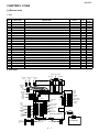
CONTENTS
CHAPTER 1. GENERAL DESCRIPTION
[1] Specifications ................................................. 1-1
[2] Operation panel.............................................. 1-2
[3] Transmittable documents ............................... 1-3
[4] Installation ...................................................... 1-4
CHAPTER 2. ADJUSTMENTS
[1] Adjustments ................................................... 2-1
[2] Diagnostics and service soft switches............ 2-7
[3] Troubleshooting ........................................... 2-30
[4] Error code table............................................ 2-31
CHAPTER 3. MECHANICAL DESCRIPTION
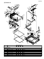
[1] Mechanical description................................... 3-1
[2] Disassembly and assembly procedures....... 3-18
CHAPTER 4. DIADRAMS
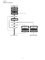
[1] Block diagram ................................................ 4-1
[2] Wiring diagram ............................................... 4-2
[3] Point-to-point diagram.................................... 4-3
CHAPTER 5. CIRCUIT DESCRIPTION
[1] Circuit description........................................... 5-1
[2] Circuit description of control PWB.................. 5-1
[3] Circuit description of LIU PWB..................... 5-19
[4]
[5]
[6]
[7]
[8]
Circuit description of power supply
PWB ............................................................5-21
Circuit description of CIS unit ......................5-22
Circuit description of operation panel
PWB ............................................................5-23
Data flow chart.............................................5-24
Troubleshooting ...........................................5-25
CHAPTER 6. CIRCUIT SCHEMATICS AND PARTS
LAYOUT
[1] Control PWB circuit .......................................6-1
[2] LIU PWB circuit ...........................................6-14
[3] Power Supply PWB circuit...........................6-17
[4] High Voltage PWB circuit.............................6-19
[5] Operation Panel PWB circuit .......................6-22
CHAPTER 7. OPERATION FLOWCHART
[1] Protocol .........................................................7-1
[2] Power on sequence.......................................7-2
CHAPTER 8. OTHER
[1] Service tools ..................................................8-1
[2] Rewriting version up the FLASH ROM ..........8-2
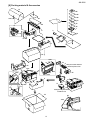
Parts Guide
Parts marked with "
" are important for maintaining the safety of the set. Be sure to replace these parts with specified ones for
maintaining the safety and performance of the set.
SHARP CORPORATION
This document has been published to be used
for after sales service only.
The contents are subject to change without notice.
AM-900U
CAUTION
This laser facsimile is a class 1 laser product that complies with 21CFR 1040.10 and 1040.11 of the CDRH or IEC60825-1 standard.
This means that this machine does not produce a hazardous laser radiation. The use of controls, adjustments or performance of procedures other than those specified herein may result in hazardous radiation exposure.
This laser radiation isn't a danger to the skin, but when an exact focusing of the laser beam is achieved on the eyes retina, there is
danger of spot damage to the retina.
The following cautions must be observed to avoid exposure of the laser beam to your eyes at the time of servicing.
1) When a problem in the laser optical unit has occurred, the whole optical unit must be exchanged as a unit, not an individual part.
2) Do not look into the machine with the main switch turned on after removing the toner/developer unit and drum cartridge.
3) Do not look into the laser beam exposure slit of the laser optical unit with the connector connected when removing and installing
the optical system.
4) The cover of Laser Printer Unit contains the safety interlock switch.
Do not defeat the safety interlock by inserting wedges or other items into the switch slot.
Laser Wave Length : 780 nm +15/-10 nm
Laser Pulse Times : 12.00 µs/7 mm
Laser Output Power : 0.4 mW ± 0.04 mW
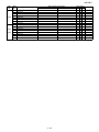
Life of consumable
Section
Toner cartridge
Drum cartridge
Paper feed
Fuser
Paper transport
Unit
Part
Replacement cartridge
(AM-90ND)
Replacement cartridge
(AM-90DR)
Transfer roller (Refer to the P/G No. 3-19)
(NROLR2525XHZZ)
Fusing unit (Refer to the P/G No. 5-901)
(DUNTK273DXH01)
Feed roller (Refer to the P/G No. 3-29)
(NROLR2333XHZZ)
AM-900
Estimated Life
3,000 prints
(at Letter/5% chart)
20,000 prints
(at Letter/5% chart)
50,000 prints
Replaced by
User
User
Service Engineer
50,000 prints
Service Engineer
Cleaning as needed
——————
5 years or 50,000 prints of early
either
——————
PRECAUTIONS FOR USING LEAD-FREE SOLDER
1. Employing lead-free solder
This model employs lead-free solder.
This is indicated by the "LF" symbol printed on the PWB and in the service manual.
The suffix letter indicates the alloy type of the solder.
Example:
Indicates lead-free solder of tin, silver and copper.
2. Using lead-free solder
When repairing a PWB with the "LF" symbol, only lead-free solder should be used. (Using normal tin/lead alloy solder may
result in cold soldered joints and damage to printed patterns.)
As the melting point of lead-free solder is approximately 40°C higher than tin/lead alloy solder, it is recommended that a
dedicated bit is used, and that the iron temperature is adjusted accordingly.
3. Soldering
As the melting point of lead-free solder (Sn-Ag-Cu) is higher and has poorer melting point (flow), to prevent damage to the
land of the PWB, extreme care should be taken not to leave the bit in contact with the PWB for an extended period of time.
Remove the bit as soon as a good flow is achieved.
The high content of tin in lead free solder will cause premature corrosion of the bit.
To reduce wear on the bit, reduce the temperature or turn off the iron when it is not required.
Leaving different types of solder on the bit will cause contamination of the different alloys, which will alter their
characteristics, making good soldering more difficult.
It will be necessary to clean and replace bits more often when using lead-free solder. To reduce bit wear, care should be
taken to clean the bit thoroughly after each use.
–i–
AM-900U
AM-900U
FAX
Service
E
Market
Manual 1. GENERAL DESCRIPTION
CHAPTER
[1] Specifications
4. Scanning specifications
1. Print specifications
Scanner type:
Resolution:
Scan speed:
Laser
Printer type:
Initial starter cartridge (included with
Toner cartridge yield*:
(continuous printing, 5% machine): Approx. 1500 pages
Replacement cartridge AM-90ND:
page coverage, letter
Approx. 3000 pages
paper)
Initial starter cartridge (included with
Drum cartridge yield*:
(continuous printing, 5% machine): 20,000 pages (average)
Replacement cartridge AM-90DR:
page coverage, letter
20,000 pages (average)
paper)
12 ppm (pages per minute)
PC print speed:
600 x 600 dpi (dots per inch)
Resolution:
* The yields may vary depending on coverage and operating conditions.
Compatibility:
Grayscale:
Color:
5. General specifications
Letter size: 20 sheets max. (20 lbs.)
Legal size: 1 sheet max. (20 lbs.)
USB 1.0/1.1 or 2.0 port (USB 1.0/1.1 or
Computer connection:
2.0 cable must be purchased separately)
Effective scanning width: 8.2” (208 mm) max.
8.2” (208 mm) max.
Effective printing width:
16-digit LCD display
Display:
250 sheets (20 lbs.)
Paper tray capacity:
(At room temperature and normal
(letter-size plain paper)
humidity)
120 V AC, 60 Hz
Power requirements:
50 - 86°F (10 - 30°C)
Operating temperature:
Humidity:
20 - 85% RH
Power consumption:
Idle: 10 W
Maximum: 690 W
Dimensions:
Width: 18.7" (475 mm)
Depth: 16.5" (420 mm)
Height: 14.6" (370 mm)
Weight:
Approx. 28.0 lbs. (12.7 kg) (including
trays and toner and drum cartridges)
Auto document feeder:
2. Copy specifications
Copy speed:
Copy quality settings:
Copy resolution settings:
Enlargement/Reduction:
Contrast settings:
Halftone (grayscale):
Multiple copies:
Maximum copy size:
CIS (Contact Image Sensor)
300/600 x 300 dpi, 300/600 x 600 dpi
Black and white:
300/600 x 300 dpi: 6 sec/page
300/600 x 600 dpi: 12 sec/page
Color and grayscale:
300/600 x 300 dpi: 18 sec/page
300/600 x 600 dpi: 36 sec/page
TWAIN, WIA
256 levels
24-bit color
12 cpm (copies per minute)
Text, Photo, Text/Photo
300 dpi, 600dpi
25% to 400%
5 levels
256 levels
Max. 99 copies per original
Document glass: Letter (8.5 x 11 in.)
Auto document feeder: Legal (8.5 x 14
in.)
3. Fax specifications
100 Speed Dial numbers
33,600 bps with automatic fallback to
lower speeds (lowest speed 2400 bps)
Approx. 3 seconds
Transmission time*:
Communication method: Super G3, G3
MMR, MR, MH
Compression scheme:
Dither
Transmission method:
2 MB (approx. 125 average letter
Memory size*:
pages)
Horizontal: 203 lines/inch (8 dots/mm)
Resolution:
Vertical: Standard: 98 lines/inch
(3.85 lines/mm)
Fine/Halftone: 196 lines/inch
(7.7 lines/mm)
Super fine: 391 lines/inch
(15.4 lines/mm)
256 levels
Halftone (grayscale):
FAX ONLY, EXT. TEL
Reception modes:
* Based on Sharp Standard Chart at standard resolution, excluding
time for protocol signals (i.e., ITU-T phase C time only).
Automatic dialing:
Modem speed:
As a part of our policy of continuous improvement, SHARP reserves the right to make design and specification changes for product improvement
without prior notice. The performance specifications figures indicated are nominal values of production units. There may be some deviations from
these values in individual units.
Trademark information
• Microsoft, Windows and Internet Explorer are trademarks of Microsoft Corporation in the
U.S.A. and other countries.
1–1
AM-900U
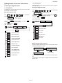
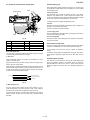
[2] Operation panel
2 3 4
1
5
6 7 8
QUALITY
CONTRAST
MENU
E-SORT
COPY
SCAN
FAX
ZOOM
9
Z
REDIAL
A
BROADCAST
!
DUPLEX SCAN PRINT STOP
ENTER
15 16
17
SPEED
HELP
10 11 12 13 14
1. Display
18 19
2. ZOOM key
Press this key to select scan mode.
12. HELP (FAX key and SCAN key)
Press the FAX key and SCAN key simultaneously to print the
HELP list, a brief guide to the operation of the machine.
Press this key to select an enlargement or reduction setting
when making a copy.
13. FAX key
3. E-SORT key
Press this key to select fax mode. When in fax mode, press
this key to select the Line Monitor function.
Press this key when making multiple copies to have the
copies collated (sorted into sets with the pages ordered 1, 2,
3..., 1, 2, 3..., etc.).
14. Alarm indicator
This blinks when the toner cartridge nears empty or the drum
cartridge is near or at the end of its life. This lights steadily
when the toner cartridge is empty, the machine is out of
paper, the print compartment cover is open, or when a paper
jam has occurred (a message will appear to indicate the
problem).
4. QUALITY key
When making a copy, press this key to select the type of
original you are copying (TEXT, PHOTO). When sending a
fax, press this key to select a resolution setting.
5. Right/left arrow keys
When making a copy, press either of these keys after
selecting an enlargement/reduction setting with the ZOOM
key to increase or decrease the setting by 1%. When sending
a fax, press either of these keys to search through your autodial fax numbers.
6. MENU key
15. DUPLEX SCAN key
Press this key to copy or fax multiple two-sided pages.
16. PRINT STOP key
Press this key to cancel a print job sent to the machine from a
computer.
17. ENTER key
Press this key, followed by the left or right arrow key, to
access special functions and settings.
Press this key to enter or select a setting.
18. BROADCAST key
7. CONTRAST key
Press this key to send the same fax to multiple destinations.
Press this key to select a contrast setting when making a copy
or sending a fax.
19. SPEED key
Press this key followed by the Start key to automatically redial
the last number dialed.
20. Number keys
Press this key to dial a fax number using an abbreviated 2digit Speed Dial number.
9. Stop key
Press this key to cancel operations before they are completed.
10. COPY key
21
11. SCAN key
This displays messages and prompts to help you operate the
machine.
8. REDIAL key
20
Use these keys to enter the number of copies, dial fax
numbers, and enter numbers and letters when storing autodial numbers.
21. Start key
Press this key to select copy mode.
Press this key when you are ready to begin copying, faxing,
or scanning. The key can also be pressed in the date and
time display of fax mode to show the percentage of memory
currently used.
1–2
AM-900U
[3] Transmittable documents
5. Automatic Document Feeder Capacity
1. Document Sizes
Number of pages that can be placed into the feeder at anytime is as
follows:
Normal size
Width
Length
Normal size: max. ADF 20 pages
5.8” - 8.5”(148 - 216 mm)
5.8” - 11”(148 - 279 mm)
Special size: single sheet only (manual feed)
NOTE: • When you need to send or copy more pages than the feeder
limit, place additional pages in feeder when last page in feeder
is being scanned.
• Place additional pages carefully and gently in feeder.
If force is used, double-feeding or a document jam may result.
(Max.)
(Min.)
6. Readable Width & Length
600mm
(Max.)
LETTER 279mm
size
The readable width and length of a document are slightly smaller than
the actual document size.
148mm
148mm
216mm
[Normal size]
Note that characters or graphics outside the effective document scanning range will not be read.
216mm
[Special size]
•
Readable width
8.2” (208mm), max
Use document carrier sheet for smaller documents.
•
With special sizes, only one sheet can be fed into the machine at a
time. Insert next page into feeder as current page is being scanned.
2. Paper Thickness & Weight
Paper weight
Paper thickness (ref.)
Paper size
Feeder capacity
10 sheets
1 sheet(Manual)
21.5 lbs.
14 lbs. ~ 42 lbs.
(80 g/m2)
(52 g/m2 ~ 157g/m2)
0.1 mm
0.1 mm ~ 0.18mm
LGL (216 mm x 355.6 mm)
A4 (210 mm x 297 mm)
LTR (216 mm x 279 mm)
A4/LTR: 10 sheets max.
LGL : 1 sheet max.
Readable width
•
Readable length
This is the length of the document sent minus 0.16” (4mm) from the
top and bottom edges.
0.16" (4mm)
3. Document Types
•
Normal paper
Readable length
Documents handwritten in pencil (No. 2 lead or softer), fountain
pen, ball-point pen, or felt-tipped pen can be transmitted.
Documents of normal contrast duplicated by a copying machine
can also be transmitted.
•
Diazo copy (blue print)
•
Diazo copy documents of a normal contrast may be transmitted.
•
Carbon copy
0.16" (4mm)
A carbon copy may be transmitted if its contrast is normal.
4. Cautions on Transmitting Documents
•
Documents written in yellow, greenish yellow, or light blue ink cannot be transmitted.
•
Ink, glue, and correcting fluid on documents must be dry before the
documents can be transmitted.
•
All clips, staples and pins must be removed from documents before
transmission.
•
Patched (taped) documents should be copied first on a copier and
then the copies used for transmission.
•
All documents should be fanned before insertion into the feeder to
prevent possible double feeds.
1–3
AM-900U
[4] Installation
2) Releasing the scanner.
1. Site selection
Before plugging in the power cord, pull the scanner release toward
you to release the scanner lock.
Take the following points into consideration when selecting a site for
this model.
• Caution: Plugging in the power cord without releasing the scanner lock may damage the machine.
ENVIRONMENT
•
The machine must be installed on a level surface.
•
Keep the machine away from air conditioners, heaters, direct sunlight, and dust.
•
Provide easy access to the front, back, and sides of the machine.
In particular, keep the area in front of the machine clear, or the original document may jam as it comes out after scanning.
•
The temperature should be between 50 - 86°F (10 - 30°C).
•
The humidity should be between 20% and 85% (without condensation).
ELECTRICITY
• In the event that you need to move the machine, push the release
back in to lock the scanner before moving (push the release in after
you have unplugged the power cord).
AC 120V, 60Hz, grounded AC (3-prong) outlet.
Caution!
•
Connection to a power source other than that specified will cause
damage to the equipment and is not covered under the warranty.
•
If your area experiences a high incidence of lightning or power
surges, we recommend that you install a surge protector for the
power and telephone lines. Surge protectors can be purchased at
most telephone specialty stores.
3) Connecting the power cord.
Plug the power cord into a 120 V, 60 Hz, grounded AC (3-prong)
outlet.
• Caution: Make sure the scanner has been released as explained
on the previous page before plugging in the power cord.
• Do not plug the power cord into any other kind of outlet. This will
damage the machine and is not covered under the warranty.
If the machine is moved from a cold to a warm place...
Condensation may form on the reading glass if machine is moved from
a cold to a warm place, this will prevent proper scanning of documents
for transmission. Turn on the power and wait approximately 2 hours
before using machine.
TELEPHONE JACK
A standard telephone jack must be located near the machine. This is
the telephone jack commonly used in most homes and offices.
•
Plugging the fax machine into a jack which is not jack may result in
damage to the machine or your telephone system. If you do not
know what kind of jack you have, or need to have one installed,
contact the telephone company.
2. Attaching the trays
• The machine does not have a power on/off switch. The power is
turned on and off by simply plugging in or unplugging the power
cord.
1) Attach the document feeder tray.
• If you area experiences a high incidence of lightning or power
surges, it is recommended that you install surge protectors for the
power and telephone lines. Surge protectors can be purchased
from your dealer or at most telephone specialty stores.
Slide the output tray into the machine as shown. When it stops, lift
the end slightly and push in so that the tray locks in place.
If you will be
using legal paper,
pull out the tray
extension.
Important: The output tray must be attached correctly or the
machine will not operate.
1–4
AM-900U
4) Connecting the telephone line cord.
1) Press the side cover release
Insert one end of the line cord into the socket on the back of the
machine marked TEL. LINE. Insert the other end into a wall telephone socket.
and then open the front cover
1
3
, open the side cover
2
,
.
Make sure that the line cord is inserted into the TEL LINE jack. Do
not insert it into the TEL. SET jack!
1
TEL.
LINE
TEL.
SET
3
2
• Caution! The fusing unit inside the print compartment becomes
very hot during operation. Do not touch the inside of the print compartment after the machine has been in operation.
2) Remove the new drum cartridge from its packaging, and remove
the tape from the top of the cartridge.
Setting the dial mode:
The machine is set for tone dialing. If you are on a pulse dial line, you must set
the fax machine for pulse dialing. Press the keys on the operation panel as
follows:
1
Make sure that the date and time
display of fax mode appears (if needed
press
FAX
) and then press
MENU
FAX SETTING
• Do not touch or allow other objects to contact the drum (the green
cylinder). This may damage the drum. If fingerprints, dust, or other
contaminants get on the drum, wipe it gently with a clean cloth.
• Exposure to light for more than several minutes will damage the
drum. Be sure to insert the drum cartridge promptly into the
machine.
Display:
2
Press
.
1: DATE&TIME SET
3
Press
.
1:TONE
4
Select the dial mode:
TONE:
5
Press
PULSE:
3) Insert the drum cartridge into the print compartment, sliding it along
the guides.
• If you find it necessary to leave the cartridge out of the machine
for move than several minutes, wrap the cartridge in black paper.
The display briefly shows
your selection, then:
5: RINGER VOLUME
repeatedly to exit.
Important: The facsimile function of this machine is not designed
for use on a line which has call waiting, call forwarding, or certain
other special services offered by your telephone company. If you
attempt to use the facsimile function in conjunction with any of
these services, you may experience errors during transmission and
reception of facsimile messages.
The facsimile function of this machine is not compatible with digital
telephone systems.
Grasp this handle to
push the cartridge in.
4) Remove the new toner cartridge from its packaging. Shake the cartridge side to side four or five times to distribute the toner evenly
within the cartridge.
3. Installing the toner cartridge and drum cartridge
The laser printer in the machine uses a toner cartridge and drum cartridge.
•
The starter toner cartridge included with the machine can print
approximately 1,500 letter-size pages at 5% page coverage.
•
When replacing the toner cartridge, use a SHARP AM-90ND toner
cartridge. One cartridge can print about 3,000 letter-size pages at
5% coverage.
•
The drum cartridge can print approximately 20,000 letter-size
pages. When replacing the drum cartridge, use a SHARP AM90DR drum cartridge.
Follow the steps below to install the toner cartridge and the drum cartridge.
Note: The quality of the toner cartridge is guaranteed for 18 months
after the date of manufacture indicated on the package. The quality of
the drum cartridge is guaranteed for 24 months after the date of manufacture indicated on the package.
1–5
AM-900U
4. Resetting the drum counter
5) Grasp the cartridge handle and insert the toner cartridge into the
print compartment, sliding it along the guides.
Each time you install a new drum cartridge, follow the steps below to
reset the drum counter to zero.
• After inserting the cartridge, press on the arrow mark to mark sure
it “clicks” into place.
• Do not touch the roller in the toner cartridge.
1
Press
MENU
Z
and then
A
or
Display:
LIFE
repeatedly until the display at right
appears.
2
Press
.
CLEAR: START KEY
DRUM COUNTER
Grasp this
handle to
insert the
cartridge.
6) Close the front cover
Press
.
4
Press
repeatedly to exit.
1: LIFE COUNTER
5. Manually resetting the toner counter
Press on this mark to
make sure the cartridge
"clicks" into place.
1
3
When a new toner cartridge is installed, the toner counter is reset in
Step 7 on the previous page. The procedure below is normally not necessary; however, it can be used in the event that you need to reset the
toner manually.
and then the side cover
2
.
• Make sure the side cover is completely closed. Otherwise, light
may enter the print compartment and damage the drum.
1
Press
Display:
MENU
and then
Z
or
A
LIFE
repeatedly until the display at right
appears.
Display:
2
Press
.
TONER EXCHANGED?
2
1
TONER COUNTER
1 = YES, 2 = NO
7) If you installed a new toner cartridge, press
to select YES
3
Press
.
4
Press
repeatedly to exit.
You can load up to 250 sheets of letter or legal paper (max. 20lbs.) in
the paper tray.
Caution! Do not use the blank side of paper that has already been
printed on.
NEW TONER?
1) Remove the output tray.
OK: PRESS START
• If you temporarily removed and then replaced an old toner carto continue
using the previous toner count. (Note: Be sure to press
,
or the machine will not alert you when the toner cartridge is out of
toner.)
8) Press
3: CLR DRUM COUNT
6. Loading printer paper
(this will reset the toner counter to zero).
tridge for maintenance or other reason, press
CLEAR: START KEY
.
9) If you installed a new drum cartridge, reset the drum counter as
explained below.
1–6
AM-900U
8. Installing the software
2) Insert a stack of paper into the tray, print side up.
• Important! The stack of paper must not be higher than the paper
height line on the paper tray.
To use the machine as a printer and scanner for your computer, you
must install the software and connect a USB cable. The CD-ROM that
comes with the machine contains the following software:
•
MFP Drivers: These consist of the printer driver that allows the
machine to be used as a printer, and the scanner driver that allows
you scan using TWAIN and WIA compliant applications.
•
Sharpdesk: This is an integrated software environment that makes
it easy to manage image files and launch applications. (Note that
Internet Explorer 5.5 or higher is required to install Sharpdesk; if
this is not installed, you will be prompted during the installation procedure to install Internet Explorer 6.0SP1® from the CD-ROM.)
Minimum system requirements
Paper height line
3) Squeeze the sides of the paper guide as shown and slide it to the
slot for the length of the paper you are loading.
Operating system:
Windows 98 SE® / Me® / 2000® / XP®
Port:
USB 2.0 or 1.1 port
Display:
800 x 600 (SVGA) with 256 colors or more
Free hard-disk space: 150 MB or more
Other requirements:
An environment in which the operating
system can freely operate.
Comments:
•
USB 2.0 Hi-Speed is only possible if your computer has a USB 2.0
port and you are using a USB 2.0 cable. In addition, the Microsoft
USB 2.0 driver must be preinstalled in your computer, or the USB
2.0 driver for Windows 2000/XP® provided through Windows
Update must be installed. Note that USB 2.0 Hi-Speed is not possible in Windows 98 SE® or Me®.
•
To scan a legal size document (the maximum size) at 1200 dpi in
full color, at least 600 MB or more of free hard disk space is
required on the drive where your operating system is installed.
Installing the software
4) Replace the output tray.
• If you loaded legal size paper (or you changed the paper size),
change the paper size setting as explained below.
•
A USB cable is required to connect the machine to your computer.
Please purchase a USB 2.0 or USB 1.0/1.1 cable. (If you wish to
use USB 2.0 Hi-Speed mode and your system meets the requirements for Hi-Speed mode, purchase a USB 2.0 cable.) The USB
cable will be connected during the software installation procedure.
•
To install the software on Windows 2000/XP® using the installer,
you must log in with administrator’s rights.
•
The windows shown in the following procedure appear in Windows
XP®. The windows that appear in other versions of Windows may
be slightly different.
1) Make sure that the USB cable is not connected to your computer.
(The cable will be connected in Step 10.)
• If the USB cable is connected, a Plug and Play window will
appear. Click the Cancel button to close the window and disconnect the cable.
7. Setting the paper size
2) Insert the Sharp CD-ROM into your computer’s CD-ROM drive.
The machine has been set at the factory to use letter size paper. If you
loaded legal size paper, you must change the paper size setting to
LEGAL.
3) In Windows XP®, click the start button, click My Computer, and
then double-click the CD-ROM icon.
1
Press
2
Press
3
Select the paper size:
COPY
SCAN
) and then
.
MENU
Display:
.
COMMON SETTING
4) Double-click the setup icon (
) in the CD-ROM window.
1:LETTER
5) Follow the instructions in the windows that appear.
LETTER:
4
(or
In Windows 98/Me/2000®, double-click My Computer on the desktop and then double-click the CD-ROM icon.
Press
LEGAL:
The display briefly shows
your selection, then:
• When the Setup Type Selection window appears, select Standard to install all of the software components (this should normally
be selected). If you only wish to install certain components, select
Custom and then select the components that you wish to install.
Note: If you wish to select the folder where Sharpdesk is installed,
select Custom.
2: AUTO CLEAR
repeatedly to exit.
1–7
AM-900U
9) The Search Setup Wizard will appear. Follow the on-screen instructions to create an index database for Sharpdesk.
10)Make sure that the power cord of the machine is not plugged in
(the machine is powered off), and then connect the USB cable.
• Insert one end of the USB cable into the USB port on the machine
and the other end into your computer’s USB port.
2000/XP®,
• In Windows
if a warning message appears at any time
regarding the Windows logo test or digital signature, be sure to
click Continue Anyway or Yes.
Note: Do not connect the AM-900 to a hub to which another AM900 is connected. If this is done, the AM-900 will not operate correctly.
6) When the Finish window appears to indicate that the selected
packages have been installed, click Close.
7) If the installation was a Standard installation, the following window
will appear. Click OK.
• If you installed the MFP drivers using a Custom installation and
did not install Sharpdesk, the following window will appear. Click
OK and go to Step 10.
11)Plug in the power cord of the machine.
• Windows XP®: Go to the procedure for completing installation of
the software.
• Windows 2000®: This completes the installation of the software.
Note: If a warning message regarding the Windows logo test
appears (the warning may appear twice), click Yes each time the
window appears. This will complete the installation of the software.
8) The following window will appear. Click Yes to restart your computer.
• Windows Me®/98SE®: This completes the installation of the software.
Completing installation of the software on Windows XP®
(Continued from Steps 10 and 11.)
1–8
AM-900U
12)In Windows XP®, the Found New Hardware Wizard will appear.
Make sure that Install the software automatically (Recommended) is selected and click Next (this will install software for
using the machine as a scanner).
14)After a brief interval, the Found New Hardware Wizard will appear
again to install software for using the machine as a printer. Make
sure that Install the software automatically (Recommended) is
selected and click Next.
• Note for Windows XP SP2®: The following window will appear
first. Select No, not this time and click Next. Continue from the
above window.
• If the following warning appears regarding the Windows logo test,
click Continue Anyway.
15)When the wizard finishes installing the printer software, click Finish
to close the Wizard. This completes the installation of the software
on Windows XP®.
Sharpdesk online guide
• If the following warning message appears regarding the Windows
logo test, click Continue Anyway.
For information on using Sharpdesk, view the Sharpdesk online
guide on the CD-ROM. To view the online guide, open the Manual
folder and then the EnglishA folder on the CD-ROM, and doubleclick SDUG_Enu.pdf.
Removing the software
In the event that you need to remove the software from your computer, open the Control Panel and select Add or Remove Programs (or Add/Remove Programs). Select SHARP AM-900
Series MFP Driver (or Sharpdesk) from the list, and click the
Change/Remove button (or the Add/Remove button). When
prompted to confirm the removal, click OK.
13)When the wizard finishes installing the scanner software, click Finish to close the wizard.
1–9
AM-900U
9. Clearing a jammed document
10. Clearing jammed printing paper
If the original document doesn’t feed properly during transmission or
copying, or DOCUMENT JAMMED appears in the display, first try
1) Press the side cover release
pressing
. If the document doesn’t feed out, open the auto
2
1
and then open the side cover
.
document feeder cover and remove it.
Important:
1
Do not try to remove a jammed without opening the auto document
feeder cover. This may damage the feeder mechanism.
1) Squeeze the cover release
1
and open the auto document
feeder cover. Open the document glass cover.
2
1
2) Push the two heater roller release levers down to release the
heater roller.
• Caution! The fusing unit (indicated in white at right) becomes
very hot during operation. Do not touch the fusing unit.
2) Remove the document.
•
The document can be removed from either the top or the bottom
slot, whichever is easiest.
3) If the jammed page is protruding from the side of the machine, gently pull it out. Take care not to tear the paper or leave any torn
pieces of paper in the print compartment.
• If this clears the jam, go to Step 5.
3) Close the auto document feeder cover, pressing down on both
sides to make sure it clicks into place.
Press down
on the marks
1 – 10
• If you are unable to clear the jam in this way, go to Step 4.
• Take care not to touch or allow other objects to contact the drum
(the green cylinder). This damage the drum.
AM-900U
4) If the jammed page cannot be pulled out directly, open the front
cover
and rotate the white knob
1
2
in the direction
shown to feed the jammed page out into the output tray.
2
1
5) After the jammed page has been removed, push the two heater
roller release levers back up.
6) Close the front cover
cover
2
1
(if you opened it) and then the side
.
1
2
1 – 11
AM-900U
11. Troubleshooting
1. Display
ADD PAPER
Check the printing paper. If the tray is empty, add
paper. If there is paper in the tray, make sure it is
inserted correctly (take out the stack, align the edges
evenly, and then reinsert it in the tray). Printing will
resume automatically when the output tray is
replaced.
BYPASS MISFEED
The paper is not inserted correctly in the bypass tray.
Remove the paper and insert it again.
BYPASS PAPER! /
IF COPY, PRESS
(alternating messages)
Paper has been inserted in the bypass tray. If the
paper has been inserted for a copy job, press
A
to
set the paper size. If the paper is for a print job, the
message can be disregarded.
COVER OPEN
One or both of the print compartment covers are
open. Make sure both covers are closed.
DATE/TIME UNSET
The date and time need to be set. Note
that the date and time settings will be lost if the
machine is unplugged or a power failure occurs.
DOCUMENT JAMMED
The original document is jammed. See the following
section, Clearing Paper Jams. Document jams will
occur if you load more than 20 pages at once or load
documents that are too thick.
The document may also jam if the receiving machine
doesn’t respond properly when you attempt to send a
fax.
Paper must be inserted in the bypass tray for a print
job or copy job that requires use of the bypass tray.
Insert the indicated size of paper in the tray.
SYSTEM ERROR [XX]
(a number appears in
“XX”)
(Refer to Printer error code/
Scanner error code)
If this message appears, unplug the power cord, wait
about 10 seconds, and then plug it back in. If the
message still appears, unplug the power cord and call
SHARP’s Customer Assistance Center at at 1-877794-8675 (U.S.A. only).
TONER EMPTY
The toner cartridge must be replaced. Printing is not
possible until the toner cartridge is replaced.
TONER NEAR EMPTY
The toner cartridge is almost out of toner
(approximately 100 pages can be printed).
TOTAL PAGE(S) 01
Number of fax pages transmitted or received.
2. Audible signals
DOCUMENT READY
A document has been inserted in the auto document
feeder and the machine is waiting for you to begin
faxing, copying, or scanning.
DRUM LIFE OVER
This appears when the drum cartridge needs
replacement.
FAX RX IN MEMORY
A fax has been received in memory because the
toner cartridge needs replacement, you have run out
of printing paper, the paper is jammed, or paper is
inserted in the bypass tray. The fax will print out
automatically when the problem is fixed.
GRP. SPACE FULL
This appears if you attempt to store a Group when
both Groups are already programmed.
LINE ERROR
Transmission or reception was not successful. Press
the STOP key to clear the message and then try
again. If the error persists, see Line error.
MEMORY IS FULL
If faxes have been received to memory because
printing is not possible (an additional message will
indicate the problem), resolve the problem so that
printing can continue (see Substitute Reception to
Memory)
If you are attempting to send a fax, see If the memory
becomes full.
If you are copying, see If MEMORY IS FULL appears.
Continuous tone
3 seconds
Indicates the end of transmission,
reception, or copying.
Intermittent tone
(3 beeps)
5 seconds
(1 second on, 1
second off)
Indicates incomplete transmission,
reception, or copying.
Rapid intermittent
tone
35 seconds
(0.7 seconds on,
0.3 seconds off)
Indicates that an extension phone
connected to the machine is off hook.
3. Printer error code (Troubleshooting Refer to page 5-26 to 5-28)
SYSTEM ERROR [P1]
The machine is preparing to or printing out a
document from memory.
NO # STORED
This appears if you attempt to search for a Speed Dial
number when none have been stored.
OFF HOOK
This appears when an extension phone connected to
The roller sensor could not detect its home position
after driving the pick up motor for the specified period.
The roller sensor could not become NOT-Active after
passing the specified period from picking up paper.
SYSTEM ERROR [P2]
MEMORY PRINTING
the machine is lifted. Only
SET BYPASS PAPER /
SIZE: XXXX
(alternating messages; a
paper size appears in
“XXXX”)
The printer controller detected the optical unit (LSU)
error.
The external interrupt signal for optical unit (LSU) or
High-voltage control did not become active after
passing the specified period.
SYSTEM ERROR [P3]
Thermistor error was detected.
SYSTEM ERROR [P4]
ROM or RAM error was detected on the printer
control unit.
SYSTEM ERROR [P5]
High temperature error was detected.
SYSTEM ERROR [P6]
Low temperature error was detected.
SYSTEM ERROR [P7]
Communication error between the main controller
and the printer controller was detected.
4. Scanner error code (Troubleshooting Refer to page 5-28)
SYSTEM ERROR [S1]
can be pressed in
fax mode when this message appears.
OUTPUT TRAY OFF
The output tray is not attached correctly. Attach it as
explained. The machine will not operate if the output
tray is not attached correctly.
PAPER JAMMED
The printing paper is jammed.
REMOVE /
BYPASS PAPER
(alternating messages)
A fax has been received to memory because paper is
inserted in the bypass tray (faxes cannot be printed
while paper is in the bypass tray). Remove the paper
from the bypass tray to allow the fax to be printed.
1 – 12
The scanner unit could not detect change point of
home postion. (ON -> OFF or OFF -> ON)
AM-900U
12. Quick setup guide
1
IMPORTANT!!
Should you require
any assistance
setting up or
operating your
product, please
DO NOT RETURN
YOUR PRODUCT
TO THE STORE.
After referring to the setup
guide and operation
manual, if you still require
assistance please consult
our web page at http://
www.sharpusa.com. From
our web page you will be
able to directly e-mail our
customer support team.
If you would like personal
assistance, please call our
Customer Assistance
Center at 1-877-794-8675
(U.S.A. only).
For detailed instructions
on setting up and using the AM-900,
see the online guide on the
CD-ROM.
To open the guide, double-click the
Manual folder on the CD-ROM,
double-click EnglishA, and then
double-click Online Manual.pdf.
(Note: Acrobat Reader 5.05 or higher
is required to view the manual.To
install Version 5.05, double-click
Acrobat Reader, English, and then
ar505eng.exe on the CD-ROM.)
3
2
Make sure you have the following
items. If any are missing, contact
your dealer or retailer.
Drum
cartridge
Toner
cartridge
Telephone
line cord
Attach the trays.
If you will be
loading legal
paper, pull the
extension out.
Output tray
4
Important:
Pull the scanner release toward
you to release the scanner lock.
Document
feeder tray
Setup
Guide
CD-ROM
Plug the power cord into a 120 V,
grounded AC (3-prong) outlet.
Caution: Be sure to release the
scanner lock (Step 3) before
plugging in the power cord.
When the tray
stops, lift the end
slightly and push in.
5
Connect the phone line cord
to the TEL. LINE jack and a
wall jack.
TEL.
LINE
TEL.
SE T
Note: An extension phone can be
connected to the TEL. SET jack with
removing the seal covering the jack.
6
Install the toner cartridge and drum cartridge.
1. Press 1 . Open the side cover
2 and then the front cover 3 .
3. Insert the drum cartridge,
sliding it along the guides.
2. Remove the drum cartridge from its
packaging, and remove the tape from
the top of the cartridge.
1
3
2
Caution!
Do not touch the fusing unit
under the side cover after the
machine has been in operation,
as it may become very hot.
5. Insert the toner cartridge, sliding it along
the guides until it clicks into place.
4. Remove the toner cartridge from its
packaging. Shake the cartridge side
to side four or five times to distribute
the toner evenly within the
cartridge.
Grasp this handle to
push the cartridge in
7. Press
6. Close the front cover 1 and
then the side cover 2 .
to select “YES” and
then press
. (This resets
8. Reset the drum cartridge counter:
MENU
a.Press
once and then
Z
or
the toner cartridge counter.)
A
Press on the arrow
mark to make sure
the cartridge clicks
into place
7
1
display.
TONER EXCHANGED?
b. Press
and then
c. Press
repeatedly to exit.
2. Insert a stack of paper
into the tray, print side up.
The stack should
not be higher
than this line
8
Set the date and time that appear
in the fax mode display.
1. Press
FAX
,
MENU
,
,
.
• The currently set date and time appear
in the display.
2. Enter a 2-digit number for the month.
4. Replace the output tray.
• To clear a mistake press
Z
.
3. Enter a two-digit number for the day
("01" to "31").
Example: the 5th
4. Enter the year (four digits)
Example:
If you loaded legal paper, see the online guide
to change the paper size setting to LEGAL.
1 – 13
5. Enter a two-digit number for the hour
and a two-digit number for the minute.
Example: 9:25
6. Press
to select A.M. or
select P.M.
Example: February
3. Squeeze the sides of the paper
guide and slide it to the slot for
the length of paper loaded.
.
1=YES, 2=NO
Load paper.
1. Remove the output tray.
2
until “LIFE” appears in the
Display:
7. Press
8. Press
ENTER
.
repeatedly to exit.
to
AM-900U
9
Install the software on your computer. (The software
allows the machine to be used as a printer and scanner.)
1. Make sure that a USB cable is not connected
to the machine and your computer. (The cable
will be connected in Step 10.)
•
•
If a cable is connected and a Plug and Play
window appears, close the window and
disconnect the cable.
Note: A USB 2.0 or 1.1 cable is required to connect the
machine to your computer. Please purchase this separately.
If you installed the MFP drivers using a Custom
installation and did not install Sharpdesk, the
following window will appear. Click OK and go to
Step 10.
2. Insert the Sharp CD-ROM into your computer’s
CD-ROM drive.
8. The following window will appear. Click Yes to restart
3. Windows XP R : Click the start button, click My
Computer, and double-click the CD-ROM icon.
your computer.
•
Windows Me R /98SE R : This completes the
installation of the software.
Completing the installation on Windows XP R
12. In Windows XP R , the Found New Hardware
Wizard will appear. Make sure that Install the
software automatically (Recommended) is
selected and click Next.
Note for Windows XP SP2 R : The first window of
the wizard will ask you if the wizard can connect
to Windows Update. Select No, not this time and
click Next.
Windows 98SE/Me/2000 R : Double click My
Computer on the desktop and double-click the
CD-ROM icon.
4. Double-click the setup icon (
) in the CD-
9. The Search Setup Wizard will appear. Follow the
on-screen instructions to create an index
database for Sharpdesk.
ROM window.
5. Follow the on-screen instructions.
•
When the Setup Type Selection window
appears, select Standard to install all of the
software components (this should normally be
selected). If you only wish to install certain
components, select Custom and then select the
components that you wish to install.
•
If a warning message appears regarding the
Windows logo test, click Continue Anyway.
13. When the wizard finishes installing the software, click
Finish to close the wizard.
14. After a brief interval, the Found New Hardware
Wizard will appear again. Make sure that Install
the software automatically (Recommended) is
selected and click Next.
10. Make sure that the machine’s power cord is not
plugged in, and then connect the USB cable to the
USB port on the machine and on your computer.
•
In Windows 2000/XP R , if a warning message
appears at any time regarding the Windows logo
test or digital signature, be sure to click Continue
Anyway or Yes.
6. When the Finish window appears to indicate that
the selected packages have been installed, click
Close.
11. Plug in the machine’s power cord.
7. If the installation was a Standard Finstallation, the
following window will appear. Click OK.
10
•
Windows XP R : Follow Steps 12 through 15 to
complete the installation of the software.
•
Windows 2000 R : This completes the installation
of the software.
Note: If a warning message regarding the
Windows logo test appears (the warning may
appear twice), click Yes each time the window
appears. This will complete the installation of the
software.
Windows XP R /Me R
4. Select SC1 (scan menu SC1) from the Select an
event list.
5. In the Actions field, select Start this program
and then select the program that you wish to link
to scan menu SC1 from the list of programs.
15. When the wizard finishes installing the software,
click Finish to close the wizard. This completes
the installation of the software on Windows XP R.
Windows 2000 R /98SE R
•
Microsoft Scanner and Camera Wizard is
selected as an example in the window below.
1. Click the Start button, point to Settings, and
select Control Panel.
2. In the Control Panel, double-click Scanners and
Cameras.
3. Select SHARP AM-900 and click Properties.
4. Click the Events tab in the SHARP AM-900
Properties.
2. Right-click the SHARP AM-900 icon and select
Properties.
3. The SHARP AM-900 Properties appear. Click
on the Events tab.
If a warning message appears regarding the
Windows logo test, click Continue Anyway.
You can scan directly from the machine by selecting scan mode and then one of scan menus
SC1 to SC6 on the operation panel. When this is done, the program linked to the selected scan
menu will automatically start on your computer and the image will be scanned to the program.
Link each scan menu that you wish to use in
scan mode to a program on your computer.
1. Windows XP R : Click the start button, Control
Panel, Printers and Other Hardware, and
Scanners and Cameras.
Windows Me R : Click the Start button, point to
Settings, select Control Panel, and double-click
Scanners and Cameras. (If Scanners and
Cameras does not appear, click view all
Control Panel options).
•
5. Select SC1 (scan menu SC1) from the Scanner
events list.
6. Click the Apply button.
7. Repeat Steps 4 through 6 as needed for any of
the other scan menus (SC2 to SC6) that you
wish to use. When finished, click the OK button.
1 – 14
6. In Send to this application, select the program
(only one) that you wish to link to scan menu SC1.
7. Click the Apply button.
8. Repeat Steps 5 through 7 for any of the other
scan menus (SC2 to SC6) that you wish to use.
When finished, click the OK button.
AM-900U
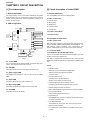
AM-900U
FAX
Service
E
Market
Manual 2. ADJUSTMENTS
CHAPTER
[1] Adjustments
1. General
Since the following adjustments and settings are provided for this
model, make adjustments and/or setup as necessary.
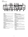
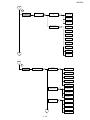
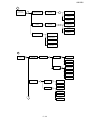
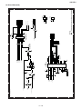
2. Adjustments of output voltage (FACTORY ONLY)
1. Install the power supply unit in the machine.
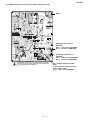
2. Set the recording paper and document.
3. When the document is loaded, power is supplied to the output
lines. Confirm that outputs are within the limits below.
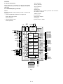
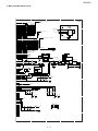
CNPN
CNSCM
CNCIS
CNOUT1
CNOUT2
CNPM
CNLSR
CNRTH
2.1. Output voltage settings
CNFRT
CNHV
CNORG
CNHPS
CNMM
CNSP
CONTROL PWB
(TOP SIDE)
CNPIN
CNBYPE CNFM
CNPUM
CNUSB
CNTCT
1
Output
+24VSUB
Voltage limits
23.04V~24.96V
+24VMAIN
23.04V~24.96V
+5VMAIN
4.75V~5.25V
+3.3VMAIN
3.201V~3.399V
Connector
Pin No.
1
2
3
4
5
6
CNPW
CNPW
MG
+24VSUB
MG
MG
+24VMAIN
+24VMAIN
CNROLSNS
7
DG
CNTCVR
8
+5VMAIN
DG
9
CNPW
14
CNLIU
CNHT
1
3
1
CN6
3
CNPW
14
1
1
+3.3VMAIN
DG
10
11
12
/HEATER ON
13
14
/PWRLY
/ZC
Connector
2
CN2
POWER SUPPLY
PWB (TOP SIDE)
Pin No.
1
2
3
CN6
+24VMAIN
N.C.
+24VS
Connector
Pin No.
1
FUSING UNIT
THERMAL
FUSE-2
INTERLOCK
SWITCH
2
3
CNHT
N
N.C.
L
Connector
Pin No.
1
2
2–1
CN2
1
2
AM-900U
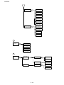
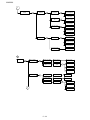
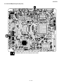
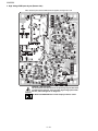
3. High voltage power check
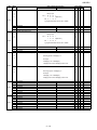
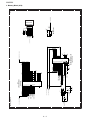
3.1. General
Note: Since the parts of this PWB cannot be supplied, change it as a unit.
CAUTION
DO NOT TOUCH!
(VR51)
CAUTION HIGH VOLTAGE AREA MAX. 4000V
Q3
D3
B1
D4
VR1
CN3
C1
C6
QJ071
J6
J5
CN4
R93
D2
R1
D8
D5
J3
D10
C5
D9
CN1
J52
VR51
C9
D1
J51
D53
D61
C7
R15
D58
D7
J12
J11
J1
J2
D62
Q52
R16
D60
Q38
J22
J21
R67
J4
D52
J42
J41
QJ005
D31
B51
C56
D54
VR31
J32
CAUTION - HIGH VOLTAGE
The unit's back cover should never be opened by
anyone other than a qualified serviceperson.
There are many high voltage parts inside the unit,
and touching them is dangerous.
J31
C65
C31
CAUTION HIGH VOLTAGE AREA MAX. 4000V
C4
R13
R14
R10
R7
R65
R3
R19
R66
R59
R4
Q1
R3
R9 R8
R3
R44 C2
R2
R14
R17
R57
R94
R63
R56
R53
C61
R51
R47
R5 R98
C55
R60
C8
R42
Q36
Q33
R41
Q32
R102
Q31
R101 C54
R71
R40
R39 R70
R66
R38
R69
R46
Q37
R79 R78
C32
Q35
R37
R62
R54
Q58
R50
C53
R75 R58
R72
R80
R81
Q34
D42
D41
R61
Q51
R64
R49
R103
R91
R43
R74
R73
C66
R48
R92
C52
Q57
R99
IC1
R100
R6
CN1
R18
R11
R52
C62
R55
C51
R76
R77
CAUTION - HIGH VOLTAGE
The unit's back cover should never be opened by
anyone other than a qualified serviceperson.
There are many high voltage parts inside the unit,
and touching them is dangerous.
R83
R36
R32 R31
R34
R33 R35
D59
R85
R86
R84
R87
R88 R89 R90
D57 D56 D55
2–2
AM-900U
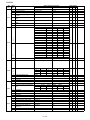
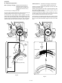
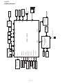
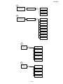
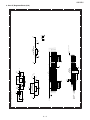
3.2. MC Voltage Check Point
Q3
D3
B1
GND (-)
D4
VR1
CN3
C1
C6
QJ071
J6
J5
D2
R1
CN4
R93
D8
D5
J3
D10
C5
D9
CN1
J52
VR51
C9
D1
D61
J51
D53
R15
D58
C7
D7
J12
J11
J1
J2
D62
Q52
D60
R16
Q38
J22
J4
D52
J42
J41
QJ005
D31
B51
C56
D54
VR31
J32
J31
C65
MC Voltage Check Point (-)
J21
R67
(There is danger of an electric shock!)
Use Measuring instrument:
Input Resistance : more than 100 MΩ
Maximum Voltage : more than 2 kV
VOLTAGE
MC : - 950 V ± 20 V (PRINTING)
MC : - 850 V ± 20 V (CLEANING)
C31
CAUTION - HIGH VOLTAGE
The unit's back cover should never be opened by anyone other than
a qualified serviceperson. There are many high voltage parts inside
the unit, and touching them is dangerous.
1) MC Voltage
Time(s)
Type
Tolerance
-570V
± 67V
-950V
± 20V
-1330V ± 67V
Voltage(v)
300Hz
2–3
AM-900U
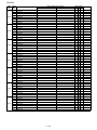
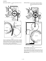
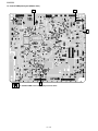
3.3. TC Voltage Check Point
Q3
D3
B1
GND (-)
D4
VR1
CN3
C1
C6
QJ071
J6
J5
D2
R1
CN4
R93
D8
D5
J3
D10
C5
D9
CN1
J52
VR51
C9
D1
D61
J51
D53
R15
D58
C7
D7
J12
J11
J1
J2
D62
TC Voltage Check Point (+)
(There is danger of an electric shock!)
Use High Voltage Tester:
Requirement of Measuring instrument:
Input Resistance : more than 100 MΩ
Maximum Voltage : more than 5 kV
Q52
D60
R16
Q38
J22
J21
R67
J4
D52
VOLTAGE
TC (+) : + 3600 V ± 72 V (PRINTING)
TC (-) : - 500 V ± 50 V (CLEANING)
J42
J41
QJ005
D31
B51
C56
D54
VR31
J32
J31
C65
C31
CAUTION - HIGH VOLTAGE
The unit's back cover should never be opened by anyone other than
a qualified serviceperson. There are many high voltage parts inside
the unit, and touching them is dangerous.
1) TC Voltage
Voltage(v)
Type
Tolerance
-3980V
-3600V
-3220V
Time(s)
300Hz
2–4
± 72V
AM-900U
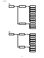
3.4. SV/DV Voltage Check Point and SV (-) Voltage Adjustment Volume
Q3
D3
B1
GND (-)
D4
VR1
CN3
C1
C6
QJ071
J6
J5
D2
R1
CN4
R93
D8
D5
J3
D10
C5
D9
CN1
J52
VR51
C9
D1
D61
J51
D53
R15
D58
C7
D7
J12
J11
J1
J2
D62
Q52
D60
R16
Q38
J22
J21
R67
J4
D52
J42
J41
QJ005
D31
B51
DV Voltage Check Point (+)
VOLTAGE
DV (+) : + 300 V ± 5 V (CLEANING)
DV (-) : - 220 V ± 5 V (PRINTING)
C56
D54
VR31
J32
J31
C65
C31
CAUTION - HIGH VOLTAGE
The unit's back cover should never be opened by anyone other than
a qualified serviceperson. There are many high voltage parts inside
the unit, and touching them is dangerous.
2–5
SV Voltage Check Point (+)
VOLTAGE
SV (+) : + 400 V ± 15 V (CLEANING)
SV (-) : - 320 V ± 15 V (PRINTING)
DV (-) Voltage adjustment Volume
VR31
It can be made to change with VR31.
In the range of ± 50V.
DV (-) : - 220 V ± 50 V (PRINTING)
AM-900U
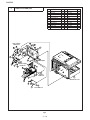
4. IC protectors replacement
5. Settings
ICPs (IC Protectors) are installed to protect the CIS unit, LIU PWB
unit, Scanner motor drive circuit, Pickup motor drive circuit, Main
motor drive circuit and IC22 circuit. ICPs protect various ICs and electronic circuits from an overcurrent condition.
5.1. Dial mode selector
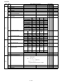
DIAL mode (Soft Switch No. SW5 Data No. 5)
Use this to set the fax machine to the type of telephone line you are
on.
The location of ICPs are shown below:
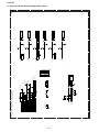
CNPIN
CNBYPE CNFM
CNCIS
CNOUT1
CNRTH
F5
F8
CNSCM
F3
CNPN
(step 1) Select "OPTIONAL SETTING".
CNFRT
KEY:
CNORG
F7
DISPLAY: 1=TONE
CNUSB
CNTCT
("2=PULSE" is displayed in the
autoscroll mode.)
CNROLSNS
CNTCVR
F6/F8:Top side
MENU
(step 2) Select "DIAL MODE".
KEY: 2 , 4
CONTROL PWB
(TOP SIDE)
CNPUM
F6
FAX
DISPLAY: FAX SETTING
CNHPS
CNSP
CNMM
CNHV
CNPM
CNLSR
CNOUT2
• The factory setting is “TONE”.
(step 3) Select, using "1" or "2".
KEY:
1 for TONE
F4
CNPW
CNIU
F3/F4/F5/F7:Bottom side
KEY:
1) F8 (KAB5002 201) is installed in order to protect IC’s from an
overcurrent generated in the CIS unit. If F8 is open, replace it with a
new one.
2 for PULSE
(step 4) End, using the "STOP" key.
(Press the "STOP" key three times.)
2) F4 (KAB5002 251) is installed in order to protect IC’s from an
overcurrent generated in the LIU PWB unit. If F4 is open, replace it
with a new one.
KEY:
3) F3 (KAB3202 202) is installed in order to protect IC’s from an
overcurrent generated in the scanner motor drive circuit. If F3 is
open, replace it with a new one.
4) F5 (KAB5002 251) is installed in order to protect IC’s from an
overcurrent generated in the IC22 circuit. If F5 is open, replace it
with a new one.
5) F6 (KAB3202 102) is installed in order to protect IC’s from an
overcurrent generated in the pickup motor drive circuit. If F6 is
open, replace it with a new one.
6) F7 (KAB2402 402) is installed in order to protect IC’s from an
overcurrent generated in the main motor drive circuit. If F7 is open,
replace it with a new one.
In addition to the replacement of F3, F4, F5, F6, F7 and F8, the factor causing F3, F4, F5, F6, F7 and F8 to open must also be
repaired. If not, F3, F4, F5, F6, F7 and F8 will open again.
Replacement parts
KAB3202 202 (Sharp code: QFS-L1027YCZZ)
KAB5002 251 (Sharp code: QFS-L2021XHZZ)
KAB3202 102 (Sharp code: QFS-L0004QCZZ)
KAB2402 402 (Sharp code: QFS-L2025XHZZ)
KAB5002 201 (Sharp code: QFS-L2016XHZZ)
2–6
AM-900U
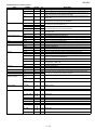
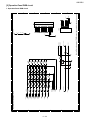
[2] Diagnostics and service soft switches
1.2. Print diagnosis
1. Entering the diagnostic mode
This diagnosis is concerned with the print which is used for production
and service support.
Entering the diagnostic mode
1.1. Fax diagnosis
This diagnosis is concerned with the main body of fax which is used
for production and service support.
9
Press MENU
display will appear.
Entering the diagnostic mode
8
: PRINTER ROM version
M/C Ver:TE53
9
Press MENU
display will appear.
8
TC84 / x x x x
Then press the START key. Select the desired item with
key and the
key or select with the rapid key.
7 , and the following
(Diag • specifications)
key
MENU
9
8
6
PRINT DIAG MODE
9
8
M/C Ver:TE53
(The alternate display of two screens.)
ENTER key.
(Diag • specifications)
MENU
the
Enter the mode with the ENTER key.
: FAX ROM version
x x x x : Check sum
Then press the START key. Select the desired item with the
and the
key or select with the rapid key.
Enter the mode with the
6 , and the following
START
7
DIAG MODE
TC84 / x x x x
U.S.A./Canada
ENTER SINGLE PRINT
(The alternate display of three screens.)
ENTER CONTINUOUS PRINT
START
ENTER COPY AGING
ENTER
SOFT SWITCH MODE
ENTER LIFE MODE
ENTER
ROM & RAM CHECK
ENTER TOP VOID ADJUST
ENTER
PANEL CHECK MODE
ENTER PRINT ADJUST
ENTER
CHECK PATTERN MODE
ENTER TEST MODE
ENTER
SIGNAL SEND MODE 1
ENTER
SIGNAL SEND MODE 2
ENTER
MEMORY CLEAR
ENTER
CIS ADJUSTING MODE
ENTER
DIAL TEST MODE
ENTER
AUTO FEEDER MODE
ENTER
FLASH MEMORY TEST
ENTER
GEAR CHANGE MODE
ENTER
FLATBED AGING
Memory clear when power is turned on
Pressing the START and STOP keys, turn on the main power, and the
following message will be indicated.
MEMORY CLEAR
[1] Key
MEMORY CLEARING
1:CLEAR
[2] Key
Stand-by display
When 1 is selected, the memory will be cleared to be ready to operation.
If 2 is selected, memory will not be cleared and the machine enters
standby mode.
2–7
AM-900U
2. Diagnostic items description
5. Storage of data
2.1. Fax diagnosis
In the following cases, the data if the soft switches set will be
stored.
2.1.1 Soft switch mode
•
It is shifted to set the next soft switch by pressing [ENTER] key.
In this mode, the soft switches are set and the soft switch list is printed.
•
It is shifted to set the next soft switch with the [>] key.
1. Operation
•
It is shifted to the last soft switch with the [<] key.
•
It is shifted to set another soft switch by inputting two digits as
the switch number.
•
Output of the soft switch list starts.
Soft switch mode screen
SOFTSWITCH MODE
6. Protocol monitor
If the SW No. 8 Data No. 5 is set to 1, the protocol monitor result is
printed after fax communication.
[ENTER] Key
SW01 = 0 1 0 1 0 0 1 0
Switch No.
2.1.2 ROM & RAM check
To check the sum value of Firmware or RAM.
1 2 3 4 5 6 7 8: Data No.
No.
1
2. Switch number selection and data setting
1) Enter two digits of a soft switch number to set the switch number. Of a switch number of non-existing soft switch is entered,
key error buzzer sounds to reject the input.
Main
2
Device
ROM
(PROGRAM FLASH)
D-RAM1(*1)
Alarm Buzzer
1 time <Short
sound>
2 times <Short
sounds>
Remarks
*1 WORK MEMORY (SDRAM 16M).
SW01 = 0 1 0 1 0 0 1 0
SW01 =
SW16 = 0 1 0 1 0 0 1 0
[ 1 ] key
[ 6 ] key
1. Display
ROM =
ROM & RAM CHECK
cursor position
ROM=OK,RAM=OK
RAM=
Start checking
by pressing [ENTER] key
2) Press [ENTER] key for setting of the next soft switch.
PRINTING
SW01 = 0 1 0 1 0 0 1 0
SW02 = 0 1 0 0 1 1 0 0
[ENTER]Key
2. Result printing
SW03 = 0 1 0 0 1 1 0 0
[ENTER]Key
cursor position
After checking, the results print starts.
3) Data number selection
2.1.3 Panel key test
(a) Pressing [>] key moves the cursor to the right.
This is used to check whether each key is normally operated or not.
When the test is started, a LED will blink (1000ms cycle) for the LED
test. During the test. After the test, the test result will be printed.
If the cursor is on data number 8, pressing [>] key shifts the cursor to data number 1 of the next switch number. If the switch
number is the final, pressing [>] key will exit the soft switch
mode.
SW01 = 0 1 0 1 0 0 1 0
cursor position
* When any numeric key is pressed during the panel test, the DTMF
signal correspond to the key number is sent to the line. If another key
is pressed the DTMF signal will stop. This function becomes valid by
changing the value of soft switch. (Default: Disable)
SW03 = 0 1 0 0 1 1 0 0
SW02 = 0 1 0 0 1 1 0 0
with the cursor on bit8
[>]Key
[>]Key
1) Flow
Press any key except [STOP] key. At this time, the name of each
key will be displayed every push of the key.
(b) Pressing [<] key moves the cursor to the left.
If the cursor is on data number 1, pressing [<] key shifts the cursor to data number 1 of the former switch number. If the switch
number is 1, pressing [<] key do not move the cursor.
SW03 = 0 1 0 1 0 0 1 0
SW03 = 0 1 0 0 1 1 0 0
PANEL CHECK MODE
SW03 = 0 1 0 0 1 1 0 0
cursor position
[<]Key
SW02 = 0 1 0 0 1 1 0 0
[<]Key
[1]Key
SW03 = 0 1 0 0 1 1 0 0
1
cursor position
[<]Key
1
PRESS EACH KEY
[ENTER] key
..... (other key)
START
[START]Key
SW01 = 0 1 0 0 1 1 0 0
To finish this mode, press [STOP] key
with the cursor on bit 1
[<]Key
Go to (a or b).
3. Data setting
a) When all keys can be inputted, the following message will be displayed.
Press the [MENU] key, and the data to the position of the cursor will
be reversed to 1 when it is 0, or to 0 when it is 1.
4. Outputting method of soft switch list
ALL KEY OK !!
In the soft switch mode, press [QUALITY] key, and the soft switch
list will be printed. If the recording paper runs out or is clogged, the
key error buzzer will sound with the process not received.
Then the screen will be all displayed in blank (Refer to (2)) and the
test result will be printed.
2–8
AM-900U
2.1.6 Signal send mode 2
b) If any key skipped, the following message will be displayed.
The specified signals about V.34 and V.8 mode transmitted in the following sequence to check the modem.
KEY ERROR !!
A key name that is not pressed yet is displayed so that this test can
be continued.
1. Press the [ENTER] key, and no signals with the loop state starts.
[ 1]
[ 2]
[ 3]
[ 4]
[ 5]
[ 6]
[ 7]
[ 8]
At that time, pressing the [STOP] key will exit this mode. And the
result will be printed.
2) Black screen
2.1.4 Check pattern mode
The effective printing area frame is printed in the specified sheet size
of the standard tray (Letter/Legal/A4).
No signals (making the loop)
33600bps (V.34bis)
31200bps (V.34bis)
28800bps (V.34)
26400bps (V.34)
24000bps (V.34)
21600bps (V.34)
19200bps (V.34)
1. Printing the pattern
[ 9]
[10]
[11]
[12]
[13]
[14]
[15]
[16]
[17]
[ENTER]Key
[ENTER]Key
Printing size depends on Paper Size setting in Common Setting.
V.34
CML ON
SIGNAL SEND2
V.34
[ENTER]Key
26400bps
[ENTER]Key
V.34
28800bps
V.34
21600bps
[ENTER]Key
V.34
The specified signals are transmitted in the following sequence to
check the modem.
[ENTER]Key
V.34
No signals (making the loop)
4800bps (V.27ter)
14400bps (V.33)
12000bps (V.33)
14400bps (V.17)
12000bps (V.17)
9600bps (V.17)
7200bps (V.17)
14400bps
[ENTER]Key
12000bps
V.17
9600bps
[ENTER]Key
V.27ter
4800bps
[ENTER]Key
V.27ter
V.33
14400bps
V.17
7200bps
7200bps
[ENTER]Key
V.34
[ENTER]Key
V.21
0 - 300bps
4800bps
[ENTER]Key
V.34
2400bps
2.1.8 CIS adjusting mode
When the "color scan" or "monochrome scan" is selected in this mode,
the scanner motor moves from its home position to the specified value.
Then, the document reading lamp is turned on.
V.29
9600bps
CIS ADJUST
[ENTER]Key
FLAG (300bps)
16800bps
Note: The following data is not cleared. Values for Printer life including
the adjusted value of printing void.
[ENTER]Key
[ENTER]Key
V.29
[ENTER]Key
2400bps
4800bps
[ENTER]Key
[ENTER]Key
7200bps
V.34
2.1.7 Memory clear
[ENTER]Key
12000bps
V.34
19200bps
[ENTER]Key
2. Pressing the [ENTER] key during transmitting ANSam signal, or
pressing the [STOP] key will stop the output of signal and exit the
mode.
[ENTER]Key
V.33
14400bps
[ENTER]Key
ANSam
V.34
[ENTER]Key
V.34
[ENTER]Key
9600bps
31200bps
Clear the backup memory including the soft switches, registration
data. After executing this mode, the memory clear report is printed.
V.27ter
[ENTER]Key
V.17
9600bps (V.29)
7200bps (V.29)
4800bps (V.27ter)
2400bps (V.27ter)
300Hz (FLAG)
2100Hz (CED)
1100Hz (CNG)
CML ON
SIGNAL SEND1
V.34
[ENTER]Key
[ENTER]Key
V.17
[ 9]
[10]
[11]
[12]
[13]
[14]
[15]
12000bps
[ENTER]Key
1. Press the [ENTER] key, and no signals with the loop state starts.
[ 1]
[ 2]
[ 3]
[ 4]
[ 5]
[ 6]
[ 7]
[ 8]
24000bps
V.34
[ENTER]Key
[ENTER]Key
2.1.5 Signal send mode 1
33600bps
[ENTER]Key
[ENTER]Key
NOW AGING
CHECKP ATTERN
16800bps (V.34)
14400bps (V.34)
12000bps (V.34)
9600bps (V.34)
7200bps (V.34)
4800bps (V.34)
2400bps (V.34)
0-300bps (V. 21)
ANSam
1: COLOR
1 key
2: MONO
2 key
[ENTER]Key
2100 Hz (CED TONE)
[ENTER]Key
The motor will move to the specified position and the reading lamp is lit on.
1100 Hz (CNG)
1. Press the [STOP] key to exit the mode.
2. Pressing the [ENTER] key during transmitting CNG signal, or
pressing the [STOP] key will stop the output of signal and exit the
mode.
2–9
AM-900U
2.1.9 Dial test mode
2.1.12 Gear change mode
The mode is used to inspect whether dialing is accurate in two kinds of
dial modes or not. All data which can be dialed in this mode are automatically called up in both PB and DP mode.
The gear to drive ADF and flatbed mechanism will be aging continuously and the number of switching will appear on the LCD.
1. Operation
When this mode is activated, the following operations will be automatically executed to their ends. Whenever the dialed content is right or
not is judged with the external instrument which is connected to the
line cable.
GEAR CHARGE MODE
[ENTER]Key
1. After pressing [ENTER] key, the CML relay is turned on, and the
following numbers are dialed in the PB mode.
“1”, “2”, “3”, “4”, “5”, “6”, “7”, “8”, “9”, “
ADF : COUNT = 00001
Drive the gear as ADF mode.
Move from Home Position to the reading direction. After
pause, move to the reading position from ADF.
“, “0”, “#”
2. And the following numbers are dialed in the DP mode.
FBED : COUNT = 00001
“1”, “5”, “9”, “0”
3. After dialing, the CML relay is turned off.
Drive the gear as Flatbed mode.
Pause and drive reversely.
ADF : COUNT = 00002
Drive the gear as ADF mode.
DIAL TEST
Move from Home Position to the reading direction.
[ENTER]Key
After pause, move to the reading position from ADF.
Go to Auto Feeder Mode
1590
123456789 #
FBED : COUNT = 00002
2.1.10 Auto feeder mode
Drive the gear as Flatbed
Pause and drive reversely.
Inserting and discharging the document can check the auto feeder.
Th is sequence will be terminated by pressing STOP k ey.
The information of document sensor (A4 sensor) and ORG sensor is
displayed when the documents are inserted to the Auto Feeder.
2. Note
1. Operation
ADF and FLATBED counter will be 0 over 65535.
Press [STOP] key to exit the mode.
AUTO FEEDER
2.1.13 Flatbed aging
[ENTER]Key
Scanner motor will be driven based on the motor speed for each resolution. By pressing the [>] key or the [<] key, you can select the motor
speed preliminary.
300 MONO
[>] Key
Feeding documents will start
by pressing ENTER key.
600 MONO
1. Operation
[>] Key
300 COLOR
[>] Key
MOTOR AGING MODE
600 COLOR
[ENTER]Key
(
300 MONO
with documents
without documents
)
A4 (A4
)
A4 (A4
ORG)
[>] Key
2. Press [STOP] key to exit the mode.
2.1.11 Flash memory test
[>] Key
The Flash memory is checked.
No.
1
Aging will start
by pressing ENTER key.
600 MONO
300 COLOR
Flash memory
NOR-Flash
Alarm Buzzer
1 time <Long sound>
[>] Key
Remarks
600 COLOR
Press STOP key to terminate this aging.
2. Press [STOP] key to exit the mode.
FLASHM EMORY
[ENTER]Key
NOW CHECKING
FLASH OK
When an error occurs, the alarm will sound.
End
Note: If this is excessively repeated, it will shorten the life of the Flash
memory.
2 – 10
AM-900U
3. Print diagnosis
3.1. Single print
In this mode, a sheet with selected pattern is printed.
1
Printing size depends on Paper Size setting in Common Setting.
2
3
2: ALL WHITE
SINGLE PRINT
[>]Key
[ENTER]Key
3: ALL BLACK
[>]Key
4
[>]Key
5
4: AREA PATTERN
1: CHECK PATTERN
6
[>]Key
7
[>]Key
5: STRIPE PATTERN
8
[>]Key
11: IDBG CHART
[>]Key
9
6: H-TONEPATTERN
[>]Key
10: SG CHRAT
[>]Key
9: 5% CHART
Figure 1 Check Pattern
7: PHIL CHART
8: GENERAL CHART
[>]Key
[>]Key
Select the desired pattern with the [>] key and [<] key and press the
[ENTER] key.
1: Check Pattern
2: All White pattern
3: All Black pattern
4: Area pattern
5: Stripe pattern
6: Halftone pattern
7: Phil chart
8: General chart
9: 5 % chart
10: SG chart
11: IDBG chart
: same as Figure 1
: Not printed
: Printed with black within print area
: Frame line is printed within print area
: Lateral stripe (Black 2 lines and White 2 lines)
: same as Figure 3
: PHIL CHART pattern
Figure 2 Halftone 2 Pattern
(a) Area pattern
It prints 30 mm long per a pattern.
1: Full Black pattern
2: Halftone 2 pattern
3: Halftone 1 pattern
4: Mesh point pattern
5: Longitudinal stripe
2 pattern
6: Lateral stripe
2 pattern
7: Lateral stripe
1 pattern
8: Full White pattern
9: Full Black pattern
(The Figure 2 is repeated.)
(The Figure 3 is repeated.)
(The Figure 4 is repeated.)
(Black 2 dots and White 2 dots are repeated in
the line.)
(Black 2 lines and White 2 lines are repeated.)
Figure 3 Halftone 1 Pattern
(Black 1 line and White 1 line are repeated.)
Figure 4 Mesh point Pattern
2 – 11
AM-900U
3.2. Continuous print
3.3. Copy aging
This mode is used for print aging.
This mode is used for COPY Aging. The document on the flatbed or
ADF will be scanned at the beginning of each cycle and printed it. The
meaning of “CYCLE”, “COUNT” and “PAGE” are same as the case
“CONTINUOUS PRINT”.
Select the desired pattern and input cycle, counter, pages for aging.
Printing size depends on Paper Size setting in Common Setting.
CONTINUOUS PRINT
[>]Key
[ENTER]Key
Printing size depends on Paper Size setting in Common Setting.
3: ALL BLACK
2: ALL WHITE
[>]Key
[>]Key
COPY AGING
4: AREA PATTERN
1: CHECK PATTERN
[ENTER]Key
[>]Key
[>]Key
[>]Key
CYCLE=000(s)
5: STRIP PATTERN
11: IDBG CHART
[>]Key
COUNT=0000(time)
6: H-TONE PATTERN
10: SG CHRAT
CYCLE=000(m)
Enter the cycle and press the [ENTER] key.
[>]Key
Enter the counter and press the [ENTER] key.
[>]Key
[>]Key
PAGE=000(sheet)
7: PHIL CHART
8: GENERAL CHART
9: 5% CHART
Enter a number of pages and press the [ENTER] key.
[>]Key
[>]Key
Start aging
Select the desired pattern with the [>]key and [<]key and press the [ENTER] key.
3.4. Life mode
This mode is used to set the life counter of the printer and the counter
of the scanner at desired values and to clear them.
[>]Key
CYCLE=000(s)
CYCLE=000(m)
LIFE MODE
Enter the cycle and press the [ENTER] key.
[ENTER]Key
COUNT=0000(time)
[>]Key
1: LIFE SETMODE
2: LIFE CLEAR
Enter the counter and press the [ENTER] key.
3.4.1 Life set mode
PAGE=000(sheet)
The values of life counter can be set in this mode.
Enter a number of pages and press the [ENTER] key.
1. Enter life set mode.
Start aging
1. Printing pattern
1: Check Pattern
2: All White pattern
3: All Black pattern
4: Area pattern
5: Stripe pattern
6: Halftone pattern
7: Phil chart
8: General pattern
9: 5 % chart
10: SG chart
11: IDBG chart
LIFE MODE
: same as Figure 1
: Not printed
: Printed with black within print area
: Frame line is printed within print area
: Lateral stripe (Black 2 lines and White 2 lines)
: same as Figure 3
: PHIL CHART pattern
[ENTER]Key
1: SCAN(ADF)
[>]Key
2: SCAN(FB)
[>]Key
3: PRINT
[>]Key
4: DRUM
[>]Key
5: TONER PAGE
2. Printing interval [CYCLE]: The time from printing end to next printing start.
[>]Key
6: TONER DOTCOUNT
Input Range: 001 to 999 seconds or 001 to 999 minutes.
[>]Key
3. Repeat printing [COUNT]: The number of printing cycle.
[ENTER]Key
0000000000
[ENTER]Key
0000000000
[ENTER]Key
0000000000
[ENTER]Key
0000000000
[ENTER]Key
0000000000
[ENTER]Key
0000000000
cursor position
2. The cursor blinks at the top data. Four counters can be selected.
Select the desired counter and input the counter value of 10 digits
using the numeric keys. Pressing the [ENTER] key changed the
counter value.
Input Range: 0001 to 9999 times.
4. Printing pages [PAGE]: The printing pages in one cycle of printing.
Input Range: 001 to 999 pages.
Note: Toner page counter cannot be changed.
Caution: These counters are not cleared after memory clear mode
is executed. If it is necessary to execute the memory clear mode on
repairing the PWB, these life counters should be set again at the
same time.
2 – 12
AM-900U
3.4.2 Life clear mode
3.6.1 Fan MD time set
This mode is used for clearing life counters.
This mode is used to set the driving time of the fan motor after stopping the main motor.
2: LIFE CLEAR
[ENTER]Key
(a)[ENTER]Key
[ENTER]Key
FAN MD_TIME SET
LI FE CLE AR
1: LIFE CLEAR ALL
FAN MD_TIME( 02 )
Cursor position
[>]Key
2: LIFE CLR EACH
[>]Key
(b)[ENTER]Key
[ENTER]Key
LI FE CLE AR
1: SCAN(ADF)
[>]Key
•
Default value: 02
•
Input Range: MIN: 00, MAX: 63
•
Unit: Minute
After entering the value, the Printer Adjust mode ends and the next
mode is displayed.
[ENTER]Key
LI FE CLE AR
2: SCAN(FB)
[>]Key
3.6.2 Tray temp.
[ENTER]Key
This mode is used to set the temperature of fixing when printing from
the standard tray.
LI FE CLE AR
3: PRINT
[>]Key
[ENTER]Key
LI FE CLE AR
4: DRUM
TRAY TEMP.
[>]Key
[ENTER]Key
[ENTER]Key
LI FE CLE AR
5: TONER
ON temp.=190 deg
[>]Key
Input temperature using the numeric keys
[>]Key
(a) Life all clear
OFF temp.=190 deg
Press the [ENTER] key, and the life counters of the printer and the life
counter of the scanner are set to 0.
Input temperature using the numeric keys
[>]Key
Note: The value for Top void is not cleared.
FEED temp.=190 deg
Input temperature using the numeric keys
(b) Life each clear
[>]Key
This mode is used to respectively clear the life counter of the printer
and the counter of the scanner. Select the desired counter and press
[ENTER] key.
TIME=10(s)
Input temperature using the numeric keys
[>]Key
Note: If “5: TONER” is executed, both “TONER PAGE” and “TONER
DOTCOUNT” are cleared.
1. ON TEMP.
The temperature to start turning on the heater.
3.5. Top void adjust
•
Default value: 190
This mode is used for adjusting the top margin for printing.
•
Range: MIN: 170, MAX: 233
Input range: [-1~06](mm)
•
Unit: Centigrade
2. OFF TEMP.
1. Press the [ENTER] key and change the adjusting value using the
“>” key and the “<“ key.
The temperature to start turning off the heater.
TOP VOID ADJUST
[ENTER]Key
TOP VOID= 04(mm)
•
Default value: 190
•
Range: MIN: 170, MAX: 233
•
Unit: Centigrade
3. FEED TEMP.
Adjust the value with the "<" the or the ">" key and press the [ENTER] key.
The temperature to start feeding the paper.
3.6. Print adjust
•
Default value: 190
This mode is used to set some values about the printer.
•
Range: MIN: 170, MAX: 233
•
Unit: Centigrade
PRINT ADJUST
4. TIME
[ENTER]Key
FAN MD_TIME SET
TRAY TEMP.
[>]Key
[>]Key
[>]Key
Warming up time after reaching the temperature that the printing
can be done.
BYPASS TEMP.
[>] Ke y
FLICKER ADJUST
PARAMETERL IST
[>]Key
2 – 13
•
Default value: 10
•
Range: MIN: 10, MAX: 63
•
Unit: Second
AM-900U
3.6.3 Bypass temp.
3.7. Test mode
This mode is used to set the temperature of fixing when printing from
the bypass tray.
This mode is used for printer aging on the two modes.
TEST MODE
BYPASS TEMP.
[ENTER]Key
[ENTER]Key
1: MOTOR AGING
ON temp.=200 deg
2: CHARGER ADJUST
Input temperature using the numeric keys
3: PAPER FEED
[>]Key
[>]Key
[>]Key
[>]Key
[>]Key
5: PRINT SIZE
4: COM TEST
Input temperature using the numeric keys
OFF temp.=200 deg
[>]Key
[>]Key
3.7.1 Motor aging
FEED temp.=200 deg
1. The motor aging starts with heater on or with heater off.
Input temperature using the numeric keys
[>]Key
MM_AGING: HT_ON
1: MOTOR AGING
TIME=10(s)
Input temperature using the numeric keys
[1]Key
[ENTER]Key
[>]Key
HT 1: ON 2: OFF
1. ON TEMP.
MM_AGING: HT_OFF
[2]Key
The temperature to start turning on the heater.
•
Default value: 200
•
Range: MIN: 170, MAX: 233
•
Unit: Centigrade
2. To exit the aging, press [STOP] key.
3.7.2 Charger adjust
This mode is used to check the high-pressure control.
1. Operation
2. OFF TEMP.
The temperature to start turning off the heater.
•
Default value: 200
•
Range: MIN: 170, MAX: 233
•
Unit: Centigrade
2: CHARGER ADJUST
[ENTER]Key
NOW ADJUSTING
1. Press the [ENTER] key to operate the mode.
3. FEED TEMP.
2. Press the [STOP] key to exit this mode.
The temperature to start feeding the paper.
•
Default value: 200
•
Range: MIN: 170, MAX: 233
•
Unit: Centigrade
3.7.3 Paper feed
This mode is used to check Mechanical Controller in the High speed
mode.
Note: This mode is not used actual printing.
4. TIME
1. Operation
Warming up time after reaching the temperature that the printing
can be done.
•
Default value: 10
•
Range: MIN: 10, MAX: 63
•
Unit: Second
3: PAPER FEED
[ENTER]Key
NOW AGING
1. Press the [ENTER] key to operate the mode.
3.6.4 Flicker adjust
2. Press the [STOP] key to exit this mode.
This mode is specified the number of table for the countermeasures of
“FLICKER”.
[E NT ER]K ey
FLICKER ADJUST
FLICKER NO.=06
•
Default value: 06
•
Input Range: MIN: 00, MAX: 63
•
Unit: -
3.6.5 Parameter list
Printing the parameter for fixing.
PARAMETER LIST
PRINTING
[E NT ER]K ey
2 – 14
AM-900U
3.7.4 COM test mode
3.7.5 Print size
You can check the communication between the main CPU and the
printer controller on this mode. Concretely, input the command number
from the main CPU and can read the response from the printer controller.
This function is prepared for the function in the future. Now there is no
meaning.
1. Operation
1. Operation
PRINT SIZE
Press [ENTER]Key
4: COM TEST
SIZE=215. 9x279. 4
[ENTER]Key
SR
SR12
=
[>]Key
EC
EC12
=10
ex)[1],[2],[3],[4]Key
, =
EEC12,34
[>]Key
ESR
=01
ex)[1],[2]Ke y
=
[>]Key
EEC
Enter paper size on bypass tray with numeric key and press the [ENTER] key.
ex)[1],[2]Ke y
= 80 13
ex)[1],[2]Ke y
ESR12
=
=15
[>]Key
(a) cursor position
1. Press the [ENTER] key to enter the mode.
2. Select the mode “SR”, “EC”, “EEC”, or “ESR” using the “<“ or the
“>” key. The “>” key can be used to select the mode only when a
cursor is in the position of (a).
3. Enter the value using the numeric keys.
“SR”, “EC”, “ESR”
• Range MIN: 00, MAX: 31
“EEC”
• Range MIN: 00, MAX: 63
4. Press the [STOP] key to exit this mode.
4. How to make soft switch setting
To enter the soft switch mode, press the following key entries in sequence.
Press MENU
9
8
7
START
ENTER
DATA No. 1 2 3 4 5 6 7 8
SW01 = 0 0 0 0 0 0 0 0
Press MENU key.
SW01 = 1 0 0 0 0 0 0 0
Press
key.
Press
key.
SW01 = 1 0 0 0 0 0 0 0
SW01 = 1 0 0 0 0 0 0 0
Bit1 - 8 are set.
SW01 = 1 0 0 0 0 0 0 0
Press ENTER key during setting.
SW02 = 0 0 0 0 0 0 0 0
Soft SW01 - SW99 are set.
SW99 = 0 0 0 0 0 0 0 0
To finish the settings halfway between
SW01 and SW99, press the STOP
key. In this case, the setting being done
to the SW No. on display will be nullified
while settings done to the preceding
SW No. remain in effect.
When the QUALITY key is pressed, the
contents of soft switches are printed.
The soft switch mode is terminated.
2 – 15
AM-900U
5. Soft switch description
5.1. Soft switch
SW
NO.
DATA
NO.
1
2
3
4
Switch setting and function
ITEM
1
0
Recall interval
Binary input
No. = 8 4 2 1
1 2 3 4 (Data No.)
EX 0 1 0 1
Initial setting
U
0
1
0
1
eg. Recall interval is set 5 min.
SW1
5
6
7
8
Recall times
Binary input
No. = 8 4 2 1
5 6 7 8 (Data No.)
EX 0 0 1 0
0
0
1
0
eg. Recall times is set 2 times
1
2
3
4
Memory retransmission times
Binary input
No. = 8 4 2 1
1 2 3 4 (Data No.)
EX 0 0 0 1
0
0
0
1
eg. Retransmission time set to 1 time.
SW2
5
6
7
8
Memory retransmission interval
Binary input
No. = 8 4 2 1
5 6 7 8 (Data No.)
EX 0 0 1 0
0
0
1
0
eg. Retransmission interval to 2 minutes.
1
2
3
4
Number of rings for auto-receive
(0: No ring receive)
Binary input
No. = 8 4 2 1
1 2 3 4 (Data No.)
EX 0 0 0 1
0
0
0
1
eg. Number of rings for auto receive is set to 1.
SW3
COPY/FAX/SCAN mode
5
6
7
8
Receive mode
Reserved
No. 5
No. 6
AUTO
COPY
0
0
2 – 16
FAX
0
1
SCAN
1
0
MANUAL
SCAN
1
1
0
0
1
0
Remarks
AM-900U
SW
NO.
DATA
NO.
Switch setting and function
ITEM
1
Distinctive Ring
SW4
1
2
3
4
5
6
7
8
Time display format
Date display format
Summer time (Daylight saving)
Flatbed document size of TX
mode
Alarm volume
OFF
STD
RING1
RING2
RING3
RING4
RING5
24 hours
Month-Day-Year
No
LETTER
No. 1
No. 2
1
2
Ringer volume
SW5
3
4
5
6
Dial mode
Header registration
Auto clear
Communication results printout
SW6
5
SW7
6
7
8
1
2
3
4
5
6
7
8
1
2
3
SW8
4
5
6
7
8
High
0
1
High
0
1
Off
30sec
0
0
0
1
Printed At error/
timer
at error
only
No. 1
0
0
No. 2
0
0
No. 3
1
0
Yes (When memory full)
No. 7
No. 8
7
8
1
2
3
4
No. 3
No. 4
PULSE
No
Off
0
0
Off
0
0
No. 1
0
0
1
0
1
0
1
Automatic printing of activity
report
Printout of total time and total
number of pages on activity report
Fax default resolution
Off
No. 6
No. 7
Reserved
ECM mode
Reserved
Header print
Footer print
Reserved
Reserved
MMR
MR
CIS transmission
DIS receive acknowledge during
G3 transmission
Non-modulated carrier in V.29
transmission mode
CNG send when manual TX
Protocol monitor
Signal monitor
Reserved
Reserved
Standard
0
0
0
No.2
No. 3
0
0
0
0
0
0
1
0
1
0
0
1
0
1
12 hours-AM/PM
Day-Month-Year
Yes
A4
Low
1
0
Middle
1
0
TONE
Yes
60sec
1
0
Send
only
Initial setting
U
No. 4
0
1
0
0
0
0
0
Low
1
1
Low
1
1
120sec
1
1
Never
prints
1
0
1
1
0
0
1
0
Always
prints
0
1
1
1
0
1
0
0
0
No (1st data is cleared when
memory full)
On
FINE
S-FINE
0
1
1
0
Off
On
Off
On
On
Off
On
On
Off
Twice
On
Off
Off
On
Once in NSF reception, twice
in DIS reception
Off
On
On
On
Off
Off
Off
2 – 17
0
0
0
0
0
1
1
0
0
0
1
0
0
0
0
0
0
0
0
0
0
0
1
1
0
0
0
1
0
0
0
1
Remarks
AM-900U
SW
NO.
SW9
DATA
NO.
1
2
3
4
5
6
7
8
SW10
ITEM
Action when RTN received
Reserved
Reserved
Reserved
Reserved
V.34 mode function in case of
manual communication
V.34 mode function
V.34 control channel communication speed
Modem speed
1
2
3
4
Reception speed fixed
Switch setting and function
1
0
Handle to no error
Handle to error
On
Off
On
2400bps
Off
1200bps
V.33 14400bps
V.33 12000bps
V.17 14400bps
V.17 12000bps
V.17 9600bps
V.17 7200bps
V.29 9600bps
V.29 7200bps
V.27ter 4800bps
V.27ter 2400bps
No
No. 5
No. 6
5
6
Compromised equalizer
No. 7
No. 8
7
8
CED tone signal interval
No. 1
No. 2
1
2
EOL detection timer
No. 3
No. 4
3
4
Processing of DIS reception after
DIS transmission
SW11
5
6
7
8
1
2
3
4
5
No. 5
No. 6
1
0
No. 1
0
0
1
1
1
1
0
0
0
0
V.1714400
BPS
1
1
1.8Km
0
1
500ms
0
1
25sec
0
1
A line is
cut
No.2
1
1
0
0
0
0
0
0
0
0
V.299600
BPS
0
1
3.6Km
1
0
750ms
1
0
5sec
1
0
Apply to
T.30
No. 3
0
1
0
1
0
1
0
1
1
0
V.27ter4800
BPS
1
0
7.2Km
1
1
1000ms
1
1
5sec
1
1
T.30 +
alpha
0
1
1
0
1
1
Reserved
Reserved
Signal transmission level
Binary input
16 8 4 2 1
1 2 3 4 5 (Data No.)
EX 0 1 1 0 1
eg. Signal transmission level is set to -10dBm
No. =
SW12
6
7
8
0
0
0Km
0
0
75ms
0
0
13sec
0
0
Command
retransmitting
0
0
Reserved
Reserved
Reserved
Initial setting
U
0
0
0
1
0
1
No. 4
0
0
0
0
1
1
1
1
0
0
1
0
0
0
0
0
0
0
0
0
0
0
0
0
0
0
0
1
1
0
1
0
0
0
2 – 18
Remarks
AM-900U
SW
NO.
DATA
NO.
1
2
3
4
5
Switch setting and function
ITEM
1
0
DTMF output level (High)
Binary input
16 8 4 2 1
1 2 3 4 5 (Data No.)
EX 0 1 1 0 0
eg. Signal transmission level is set to -10dBm
No. =
SW13
6
7
8
1
2
3
4
5
Reserved
Reserved
Reserved
DTMF output level (Low)
6
7
8
1
2
3
4
Reserved
Reserved
Reserved
V.34 mode transmission speed
Binary input
16 8 4 2 1
1 2 3 4 5 (Data No.)
EX 1 0 0 0 0
eg. Signal transmission level is set to -10dBm
No. =
SW14
Sending speed = 2400(bps) x n
Example:
Initial setting
U
0
1
1
0
0
0
0
0
1
0
0
0
0
0
0
0
1
1
1
0
2400(bps) x 12 = 28800(bps)
2400(bps) is set for N=0. 33600(bps) is set for N=15.
SW15
5
6
7
8
V.34 mode receiving speed
Receving speed = 2400(bps) x n
Example:
1
1
1
0
2400(bps) x 12 = 28800(bps)
2400(bps) is set for N=0. 33600(bps) is set for N=15.
SW16
SW17
1
2
3
4
5
6
7
8
1
2
3
4
5
6
7
8
Reserved
Reserved
Reserved
Reserved
Reserved
Reserved
Reserved
Reserved
Reserved
Reserved
Reserved
Reserved
Reserved
Reserved
Reserved
Reserved
0
0
0
0
0
0
0
0
0
0
0
0
0
0
0
0
2 – 19
Remarks
AM-900U
SW
NO.
SW18
DATA
NO.
1
2
3
4
5
6
7
8
SW19
Switch setting and function
ITEM
Key push sound
Line monitor type
Pause time
Ringing Display (if ringer volume
is OFF)
Dial tone detection (before autodial)
Busy tone detection (after autodial)
Recall Control (for FCC Part68)
Line monitor
CI signal frequency
1
On
Fax and Dial
4sec
On
Off
dial only
2sec
Off
On
Off
0
On
Off
1
On
On
Off
Off
No.2
0
0
0
0
1
1
1
1
0
No. 6
0
0
1
1
0
0
1
1
FW
N
1
0
No. 1
0
0
0
0
0
0
0
0
1
No. 5
0
0
0
0
1
1
1
1
11.6-76.9
14.0-76.9
14.5-76.9
15.5-76.9
20.0-58.8
20.0-66.6
19.6-76.9
25.0-58.8
35.0-76.9
1
2
3
4
CI signal OFF detect enable time
5
6
7
8
1
Method of detecting CI frequency
Pulse Format of D.P.
200ms
300ms
350ms
400ms
500ms
700ms
1200ms
Not used
Modem
N+1
Inter digit pause time
SW20
SW21
SW22
2
3
4
5
6
7
8
1
2
3
4
5
6
7
8
1
2
3
4
5
6
7
8
Pulse Mark/Break Ratio
Reserved
Reserved
Reserved
Reserved
DTMF sending by panel test mode
Number of busy tone pulse detection
Reserved
Reserved
Reserved
Reserved
Print mode when printer life over
Print mode when drum life over
Print mode when toner empty
Print mode when toner unsuitable
Print mode when paper size error
Print mode when paper tray
removed
Reserved
Reserved
Initial setting
U
1
0
0
1
0
No. 2
No. 3
No. 4
40/60
800ms
0
0
0
840ms
0
0
1
2pulse
0
0
4pulse
0
1
Yes
No. 3
No. 4
880ms
0
1
0
33/67
No
6pulse
1
0
No. 3
0
0
1
1
0
0
1
1
0
No. 7
0
1
0
1
0
1
0
1
No. 4
0
1
0
1
0
1
0
1
0
900ms
0
1
1
1000ms
1
0
0
8pulse
1
1
0
0
0
0
1
0
1
0
0
0
0
1
1
0
0
0
0
0
Continue
Continue
Continue
Continue
Continue
Continue
Stop
Stop
Stop
Stop
Stop
Stop
0
0
0
1
0
1
1
1
0
0
1
0
Continue
Continue
Stop
Stop
1
1
2 – 20
Remarks
AM-900U
SW
NO.
DATA
NO.
ITEM
Paper size at tray
SW23
SW24
1
2
3
4
5
6
7
8
1
2
3
4
5
6
7
8
No. 1
No. 2
No. 3
No. 4
Reserved
Reserved
Reserved
Reserved
Automatic reduce of receive
Reserved
Reserved
Reserved
Reserved
Reserved
Reserved
Reserved
100%
Copy default content type
No. 1
No. 2
1
2
Copy default quality
SW25
No. 3
No. 4
3
4
5
6
7
8
Copy default center contrast (for
TEXT)
Copy default center contrast (for
PHOTO)
No. 5
No. 6
No. 7
No. 8
Speaker volume
SW26
1
2
3
4
5
6
7
8
No. 1
No. 2
Reserved
Reserved
Reserved
Reserved
Reserved
Reserved
Fax default center contrast
Darker
Dark
Normal
Light
Lighter
Normal
1
2
3
Copy default contrast
SW27
4
5
6
7
8
Switch setting and function
1
0
Letter
A4
Legal
N/A
0
0
0
x
0
0
0
x
0
0
1
x
0
1
0
x
Darker
Dark
Normal
Light
Lighter
Normal
Auto reduce
Text
0
0
300
0
0
Dark
0
0
Dark
0
0
Low
0
0
Photo
1
0
600
1
1
Normal
0
1
Normal
0
1
Middle
0
1
No. 1
No. 2
0
0
0
0
0
1
0
1
1
0
Other setting
No. 4
No. 5
0
0
0
0
0
1
0
1
1
0
Other setting
Reserved
Reserved
2 – 21
Initial setting
U
0
0
0
0
0
0
0
0
0
0
0
0
0
0
0
0
0
0
0
0
Light
1
0
Light
1
0
High
1
0
No. 3
0
1
0
1
0
No. 6
0
1
0
1
0
Normal
1
1
Normal
1
1
Low
1
1
0
1
1
0
0
0
0
0
0
0
0
0
0
1
0
0
1
0
0
0
Remarks
AM-900U
SW
NO.
SW28
SW29
SW30
SW31
SW32
SW33
SW34
DATA
NO.
1
2
3
4
5
6
7
8
1
2
3
4
5
6
7
8
1
2
3
4
5
6
7
8
1
2
3
4
5
6
7
8
1
2
3
4
5
6
7
8
1
2
3
4
5
6
7
8
1
2
3
4
5
6
7
8
Switch setting and function
ITEM
Reserved
Reserved
Reserved
Reserved
Reserved
Reserved
Reserved
Reserved
Reserved
Reserved
Reserved
Reserved
Reserved
Reserved
Reserved
Reserved
Reserved
Reserved
Reserved
Reserved
Reserved
Reserved
Reserved
Reserved
USB high speed setting
Reserved
Reserved
Reserved
Reserved
Reserved
Reserved
Reserved
Reserved
Reserved
Reserved
Reserved
Reserved
Reserved
Reserved
Reserved
Reserved
Reserved
Reserved
Reserved
Reserved
Reserved
Reserved
Reserved
Reserved
Reserved
Reserved
Reserved
Reserved
Reserved
Reserved
Reserved
1
Disable
0
Enable
2 – 22
Initial setting
U
0
1
0
1
1
0
1
0
0
0
1
0
0
1
0
0
0
0
0
0
0
0
0
0
0
0
0
0
1
0
0
0
0
0
1
0
0
0
0
0
0
0
0
0
0
0
0
0
0
0
0
0
0
0
0
0
Remarks
AM-900U
SW
NO.
SW35
SW36
SW37
SW38
SW39
SW40
SW41
DATA
NO.
1
2
3
4
5
6
7
8
1
2
3
4
5
6
7
8
1
2
3
4
5
6
7
8
1
2
3
4
5
6
7
8
1
2
3
4
5
6
7
8
1
2
3
4
5
6
7
8
1
2
3
4
5
6
7
8
ITEM
Switch setting and function
1
Reserved
Reserved
Reserved
Reserved
Reserved
Reserved
Reserved
Reserved
Reserved
Reserved
Reserved
Reserved
Reserved
Reserved
Reserved
Reserved
Reserved
Reserved
Reserved
Reserved
Reserved
Reserved
Reserved
Reserved
Reserved
Reserved
Reserved
Reserved
Reserved
Reserved
Reserved
Reserved
Reserved
Reserved
Reserved
Reserved
Reserved
Reserved
Reserved
Reserved
Reserved
Reserved
Reserved
Reserved
Reserved
Reserved
Reserved
Reserved
Reserved
Reserved
Reserved
Reserved
Reserved
Reserved
Reserved
Reserved
2 – 23
0
Initial setting
U
0
0
0
0
0
0
0
0
0
0
0
0
0
0
0
0
0
0
0
0
0
0
0
0
0
0
0
0
0
0
0
0
0
0
0
0
0
0
0
0
0
0
0
0
0
0
0
0
0
0
0
0
0
0
0
0
Remarks
AM-900U
SW
NO.
SW42
SW43
SW44
SW45
SW46
SW47
SW48
DATA
NO.
1
2
3
4
5
6
7
8
1
2
3
4
5
6
7
8
1
2
3
4
5
6
7
8
1
2
3
4
5
6
7
8
1
2
3
4
5
6
7
8
1
2
3
4
5
6
7
8
1
2
3
4
5
6
7
8
ITEM
Switch setting and function
1
Reserved
Reserved
Reserved
Reserved
Reserved
Reserved
Reserved
Reserved
Reserved
Reserved
Reserved
Reserved
Reserved
Reserved
Reserved
Reserved
Reserved
Reserved
Reserved
Reserved
Reserved
Reserved
Reserved
Reserved
Reserved
Reserved
Reserved
Reserved
Reserved
Reserved
Reserved
Reserved
Reserved
Reserved
Reserved
Reserved
Reserved
Reserved
Reserved
Reserved
Reserved
Reserved
Reserved
Reserved
Reserved
Reserved
Reserved
Reserved
Reserved
Reserved
Reserved
Reserved
Reserved
Reserved
Reserved
Reserved
2 – 24
0
Initial setting
U
0
0
0
0
0
0
0
0
0
0
0
0
0
0
0
0
0
0
0
0
0
0
0
0
0
0
0
0
0
0
0
0
0
0
0
0
0
0
0
0
0
0
0
0
0
0
0
0
0
0
0
0
0
0
0
0
Remarks
AM-900U
SW
NO.
SW49
SW50
l
SW99
DATA
NO.
1
2
3
4
5
6
7
8
1
2
3
4
5
6
7
8
ITEM
Switch setting and function
1
Reserved
Reserved
Reserved
Reserved
Reserved
Reserved
Reserved
Reserved
Reserved
Reserved
Reserved
Reserved
Reserved
Reserved
Reserved
Reserved
2 – 25
0
Initial setting
U
0
0
0
0
0
0
0
0
0
0
0
0
0
0
0
0
Remarks
AM-900U
5.2. Soft switch function description
SW5 No. 5 Dial mode
SW1 No. 1 ~ No. 4 Recall interval
Switch the type according to the telephone circuit connected to the
facsimile.
Choice is made for a recall interval for speed and rapid dial numbers.
Use a binary number to program this. If set to 0 accidentally, 1 will be
assumed.
0: PULSE DIAL
1: TONE DIAL
SW1 No. 5 ~ No. 8 Recall times
SW5 No. 6 Header registration
Choice is made as to how many recall times should be made. Use a
When setting this switch to "1", registering senders is protected.
binary number to program this.
SW5 No. 7, No. 8 Auto Clear
SW2 No. 1 ~ No. 4 Memory retransmission times
The number of memory retransmissions is set.
Used to set the retention time for the copy settings. After the specified
auto clear time elapses, the default settings return.
SW2 No. 5 ~ No. 8 Memory retransmission interval
SW6 No. 1 ~ No. 3 Communication results printout
The interval between memory retransmissions is set.
It is possible to obtain communication results after each transaction.
Normally, the switch is set (No. 1: 0, No. 2: 0, No. 3: 1) so that the
communication result is produced only a communication error is
encountered.
SW3 No. 1 ~ No. 4 Number of rings for auto-receive
(0: No ring receive)
When the machine is set in the auto receive mode, the number of rings
before answering can be selected. It may be set from one to nine rings
using a binary number. If the soft switch was set to 1, a direct connection is made to the facsimile. If it was set to 0 accidentally, receive ring
is set to 1. If it was above 9, receive rings are set to 9.
If No. 1 was set to 1, No. 2 was set to 1 and No. 3 was set to 0, the
communication result will be produced every time a communication is
done, even if the communication was successful. If No. 1 was set to 0,
No. 2 to 1 and No. 3 to 0, the communication result will be produced
every transmission. Setting No. 1 to 1 No. 2 to 0 and No. 3 to 0 will disable this function. No transaction report will be printed. If No. 1 was set
to 0, No. 2 to 0 and No. 3 to 0, the communication result is produced
only after a timer and memory transmission or when a communication
error is encountered.
SW3 No.5, No.6 COPY/FAX/SCAN mode
An operation mode for each copy, fax, or PC scan is set.
SW-3 No. 7 Receive mode
SW6 No. 4 Automatic printing of activity report
Auto/extension telephone receiving mode is set.
This soft switch is used to select; whether or not to produce the activity
report when the memory is full (about 30 items). An activity report can
be produced from Report&List mode.
SW-3 No. 8 Reserved
Set to “0”.
After producing the activity report, all the data in the memory will be
cleared. When the switch function is set to "0" (NO), the data in memory will be deleted from the oldest as it reaches the maximum memory
capacity (approx. 30 items).
SW-4 No. 1 ~ No. 4 Distinctive ringing
When the ringing setting is turned off, all of the CI signal are received.
When any of the standard, and ring patterns 1 through 3 is selected for
the ringing setting, only the selected CI signal is received.
CI signal patterns
SW6 No. 5 Print out total time and total number of pages on activity report
The CI signal patterns consists of the standard pattern, and ring patterns 1 through 7. The standard pattern is the conventional one.
Used to print out the total communication time and the total pages
sent/received on the activity report.
SW4 No. 5 Time display format
SW6 No. 6, No. 7 Fax default resolution
When this switch is set to "0", time is displayed in 12-hour system.
Used to set the transmission mode which is automatically selected
when the QUALITY key is not pressed. In the copy mode, however,
the fine mode is automatically selected unless the QUALITY key is
manually set to another mode.
When set to "1", 24-hour system.
SW4 No. 6 Date display format
Used to select date display/print formats.
SW6 No. 8 Reserved
0: DAY-Month-Year
Set to "0".
1: Month-Day-Year
SW7 No. 1 ECM mode
SW4 No. 7 Summer time (Daylight saving)
Used to determine ECM mode function.
The daylight saving function ON/OFF is set.
SW7 No. 2 Reserved
SW4 No. 8 Flatbed document size of TX mode
Set to "0".
Used to set a document scan length for fax transmission from the flatbed.
SW7 No. 3 Header print
Used to set volume of the end buzzer or error buzzer for facsimile
transmission/reception.
When it is set at 0, sender’s name, sending page number and so on
are automatically printed in the recording paper on the receiving side
during transmission. Thus, the sender can be known on the receiving
side.
SW5 No. 3, No. 4 Ringer volume
0: Applied.
Ringer volume:
1: Not applied.
SW5 No. 1, No. 2 Alarm volume
The calling sound volume of CI signal receiving is set.
2 – 26
AM-900U
SW7 No. 4 Footer print
SW9 No. 7 V.34 mode function
When set to "1", the date of reception, the sender machine No., and
the page No. are automatically recorded at the end of reception.
Used to select the V.34 mode for communication when set to “1” communication method is V.34 mode.
SW7 No. 5, No.6 Reserved
SW9 No. 8 V.34 control channel communication speed
Set to "0".
Used to select the control channel communication speed for V.34
mode.
SW7 No. 7 MMR
SW10 No. 1 ~ No. 4 Modem speed
MMR (Modified MR) selects presence of the compression function.
Used to determine the initial modem speed. The default is
14400BPS(V.17). It may be necessary to program it to a slower speed
when frequent line fallback is encountered, in order to save the time
required for the fallback procedure.
SW7 No. 8 MR
MR (Modified READ) selects presence of the compression function.
SW8 No.1 CSI transmission
SW10 No. 5, No. 6 Reception speed fixed
CSI signal contains the sender’s phone number registered in the
machine. If this switch is set to "1", no sender’s name will be printed at
the receiving side.
The transferable speed of modem in the receiving mode is set.
SW10 No. 7, No. 8 Compromised equalizer
SW8 No. 2 DIS receive acknowledge during G3 transmission
The specific line equalizer is inserted.
Used to make a choice of whether reception of NSF (DIS) is acknowledged after receiving two NSFs (DISs) or receiving one NSF (two
DISs). It may be useful for overseas communication to avoid an echo
suppression problem, if set to 1.
No. 1 No. 2
0 0: The line equalizer built in the modem is turned off.
0 1: Line equalizer corresponding to 1.8 km.
SW8 No. 3 Non-modulated carrier in V.29 transmission mode
1 0: Line equalizer corresponding to 3.6 km.
Though transmission of a non-modulated carrier is not required for
transmission by the V29 modem according to the CCITT Recommendation, it may be permitted to send a non-modulated carrier before the
image signal to avoid an echo suppression problem. It may be useful
for overseas communication to avoid an echo suppression problem, if
set to 1.
0 1: Line equalizer corresponding to 7.2 km.
SW11 No. 1, No. 2 CED tone signal interval
For international communication, the 2100Hz CED tone may act as an
echo suppressor switch, causing a communication problem. Though
this soft switch is normally set to "0", it should be set to "1" so as to
change the time between CED tone and DIS signal from 75ms to
500ms to eliminate the communication problem caused by echo.
SW8 No. 4 CNG send when manual TX
CNG signal sending ON/OFF in case of manual transmission is set.
SW11 No. 3, No. 4 EOL detection timer
SW8 No. 5 Protocol monitor
Used to make a choice of whether to use the 25-second or 13-second
timer for detection of End of line This is effective to override communication failures with some facsimile models that have longer End of line
detection.
Normally set to "0". If set to "1", communication can be checked, in
case of troubles, without using a G3 tester or other tools. When communication FSK data transmission or reception is made, the data is
taken into buffer. When communication is finished, the data analyzed
and printed out. When data is received with the line monitor (SW7-No.
7) set to "1" the reception level is also printed out.
SW11 No. 5, No. 6 Processing of DIS reception after DIS transmission
When receiving, operation in case of DIS reception after DIS transmission is selected. Retransmitting command: To retransmit DIS in disregard of DIS reception.
SW8 No. 6 Signal monitor
Normally set to "0". If set to "1", the transmission speed and the reception level are displayed on the LCD. Used for line tests.
Breaking circuit: To break circuit instantly. (Abnormal finish)
SW8 No. 7 Reserved
T. 30: To operate in accordance with T. 30.
Set to "0".
T. 30+<: To operate in accordance with T. 30+<. (To operate differently
according to cases.)
SW8 No.8 Reserved
SW11 No. 7, No.8 Reserved
Set to "1".
Set to "0".
SW9 No.1 Action when RTN received
SW12 No. 1 ~ No. 5 Signal transmission level
The operation is set when the RTN signal is received in the G3 transmission mode.
Used to control the signal transmission level in the range of -0dB to 31dB.
SW9 No. 2, No.3 Reserved
SW12 No. 6 ~ No.8 Reserved
Set to "0".
Set to "0".
SW9 No. 4 Reserved
Set to "1".
SW13 No. 1 ~ No. 5 DTMF output level (High)
SW9 No. 5 Reserved
To set the level to output high group DTMF signals. -15 to 0 dBm (0.5
dBm unit)
Set to "0".
SW13 No. 6 ~ No. 8 Reserved
SW9 No. 6 V.34 mode function in case of manual communication
Set to "0".
Used to select whether the V.34 mode is made valid when automatically transmitting/receiving.
SW14 No. 1 ~ No. 5 DTMF output level (Low)
To set the level to output low group DTMF signals. -15 to 0 dBm (0.5
dBm unit)
2 – 27
AM-900U
SW14 No. 6 ~ No. 8 Reserved
SW21 No. 2 DTMF sending by panel test mode
Set to "0".
With this switch set to “1”, the DTMF signal is sent when a numeric key
is pressed in the panel test mode.
SW15 No. 1 ~ No. 4 V.34 mode transmission speed
SW21 No. 3, No. 4 Busy tone detection pulse number
Used to determine the initial modem speed when communication
method is V.34 transmission mode.
Used to set detection of Busy tone intermittent sounds.
SW15 No. 5 ~ No. 8 V.34 mode receiving speed
SW21 No. 5 Reserved
Used to determine the initial modem speed when communication
method is V.34 reception mode.
Set to "0".
SW16 No. 1 ~ No. 8 Reserved
Set to "1".
SW21 No. 6 Reserved
Set to "0".
SW21 No. 7 Reserved
SW17 No. 1 ~ No. 8 Reserved
Set to "0".
Set to "0".
SW21 No. 8 Reserved
SW18 No. 1 Key push sound
Set to "1".
Used to toggle the key sound between on and off.
SW22 No. 1 Print mode when printer life over
SW18 No. 2 Line monitor type
The time period to monitor the sound on the line is set.
Used to set whether the printing operation stops or not when the
PRINTER LIFE OVER error occurs.
0: From the start of dialing, and until the call reaches receiving party
SW22 No. 2 Print mode when drum life over
1: From the start of dialing to the end of the communication
Used to set whether the printing operation stops or not when the
DRUM LIFE OVER error occurs.
SW18 No. 3 Pause time
The dial pause time is set.
SW22 No. 3 Print mode when toner empty
SW18 No. 4 Ringing display (if ringer volume is OFF)
Used to set whether the printing operation stops or not when the
TONER EMPTY error occurs.
When set to “1” and ringer volume is OFF, “RINGING” display informs
you that the CI signals are received.
SW22 No. 4 Print mode when toner unsuitable
Used to set whether the printing operation stops or not when the
TONER UNSUITABLE error occurs.
SW18 No. 5 Dial tone detection (before auto dial)
When set to “1”, a number is dialed after detecting the dial tone.
SW22 No. 5 Print mode when size error
SW18 No. 6 Busy tone detection (after auto dial)
When set to “1”, the busy tone is detected after dialing a number.
Used to set whether the printing operation stops or not when the SIZE
ERROR occurs.
SW18 No. 7 Recall control (for FCC part68)
SW22 No. 6 Print mode when paper tray removed
Recalling fixed only one time when dialing was unsuccessful without
detecting busy tone signal.
Used to set whether the printing operation stops or not when the
PAPER TRAY REMOVED error occurs.
SW18 No. 8 Line monitor
SW22 No. 7, No. 8 Reserved
When set to “1”, sound on the line is monitored in transmission.
Set to "1".
SW19 No.1 ~ No. 4 CI signal frequency
SW23 No. 1 ~ No. 4 Paper size at tray
Used to set a frequency that is considered as the CI signal.
The paper size in the tray is set.
SW19 No. 5 ~ No. 7 CI signal OFF detect enable time
SW23 No. 5 ~ No. 8 Reserved
Used to set the maximum length of CI signal OFF time, which is used
to determine a sequence of CI signals.
Set to "0".
SW24 No. 1 Automatic reduce of receive
SW19 No. 8 Method of detecting CI frequency
If set to 1, it is reduced automatically.
CI frequency detection method is set.
SW24 No. 2 ~ No. 8 Reserved
SW20 No. 1 Pulse format of D.P.
Set to "0".
Used to set pulse format of D.P. mode.
SW25 No. 1, No. 2 Copy default content type
SW20 No. 2 ~ No. 4 Inter digit pause time
The default copy scanning quality is set.
Used to set the pause time between pulses
SW25 No. 3, No. 4 Copy default quality
SW20 No. 5 Pulse Make/Break ratio.
Copy scanning resolution is set.
Used to set pulse ratio of D.P. mode.
SW25 No. 5, No. 6 Copy default center contrast (for TEXT)
SW20 No. 6 ~ No. 8 Reserved
When the copy scanning quality is set to the TEXT mode, this switch is
used to set the reference contrast of the center value for the default
contrast setting (SW27 No. 4 ~ No. 6).
Set to "0".
SW21 No. 1 Reserved
Set to "0".
2 – 28
AM-900U
SW25 No. 7, No. 8 Copy default center contrast (for PHOTO)
SW31 No. 7, No. 8 Reserved
When the copy scanning quality is set to the PHOTO mode, this switch
is used to set the reference contrast of the center value for the default
contrast setting (SW27 No. 4 ~ No. 6).
Set to "0".
SW32 No. 1, No. 2 Reserved
Set to "0".
SW26 No. 1, No. 2 Speaker volume
SW32 No. 3 Reserved
The line monitor volume is set.
Set to "1".
SW26 No. 3 ~ No. 8 Reserved
SW32 No. 4 ~ No. 8 Reserved
Set to "0".
Set to "0".
SW27 No. 1 ~ No. 3 Fax default center contrast
SW33 No. 1 ~ No. 8 Reserved
Used to set the reference contrast of the center value for the fax contrast setting.
Set to "0".
SW27 No. 4 ~ No. 6 Copy default contrast
SW34 No. 1 ~ No. 8 Reserved
The default is set in the copy contrast setting.
Set to "0".
SW27 No. 7, No. 8 Reserved
SW35 No. 1 ~ No. 8 Reserved
Set to "0".
Set to "0".
SW28 No. 1 Reserved
SW36 No. 1 ~ No. 8 Reserved
Set to "0".
Set to "0".
SW28 No. 2 Reserved
SW37 No. 1 ~ No. 8 Reserved
Set to "1".
Set to "0".
SW28 No. 3 Reserved
SW38 No. 1 ~ No. 8 Reserved
Set to "0".
Set to "0".
SW28 No. 4, No. 5 Reserved
SW39 No. 1 ~ No. 8 Reserved
Set to "1".
Set to "0".
SW28 No. 6 Reserved
SW40 No. 1 ~ No. 8 Reserved
Set to "0".
Set to "0".
SW28 No. 7 Reserved
SW41 No. 1 ~ No. 8 Reserved
Set to "1".
Set to "0".
SW28 No. 8 Reserved
SW42 No. 1 ~ No. 8 Reserved
Set to "0".
Set to "0".
SW29 No. 1, No. 2 Reserved
SW43 No. 1 ~ No. 8 Reserved
Set to "0".
Set to "0".
SW29 No. 3 Reserved
SW44 No. 1 ~ No. 8 Reserved
Set to "1".
Set to "0".
SW29 No. 4, No. 5 Reserved
SW45 No. 1 ~ No. 8 Reserved
Set to "0".
Set to "0".
SW29 No. 6 Reserved
SW46 No. 1 ~ No. 8 Reserved
Set to "1".
Set to "0".
SW29 No. 7, No. 8 Reserved
SW47 No. 1 ~ No. 8 Reserved
Set to "0".
Set to "0".
SW30 No. 1 ~ No. 8 Reserved
SW48 No. 1 ~ No. 8 Reserved
Set to "0".
Set to "0".
SW31 No. 1 USB high speed setting
SW49 No. 1 ~ No. 8 Reserved
Used to set whether the USB high speed mode is activated or not.
Set to "0".
SW31 No. 2 ~ No. 4 Reserved
SW50 ~ SW99 No. 1 ~ No. 8 Reserved
Set to "0".
Set to "0".
SW31 No. 5 Reserved
Set to "1".
SW31 No. 6 Reserved
Set to "0".
2 – 29
AM-900U
[3] Troubleshooting
•
Refer to the following actions to troubleshoot any of the problems
mentioned in 1-4.
Apply line equalization SOFT SWITCH 10-7, 8.
May be used in case [1] [2] [3] [4].
•
Slow down the transmission speed SOFT SWITCH 10-1, 2, 3, 4.
May be used in case [2] [3].
•
Replace the LIU PWB.
May be used in all cases.
•
Replace the control PWB.
May be used in all cases.
•
If transmission problems still exist on the machine, use the following format and check the related matters.
[1] A communication error occurs.
[2] Image distortion produced.
[3] Unable to do overseas communication.
[4] Communication speed slow due to FALLBACK.
•
In crease the transmission level SOFT SWITCH 12-1, 2, 3, 4, 5.
May be used in case [1] [2] [3].
•
Decrease the transmission level SOFT SWITCH 12-1, 2, 3, 4, 5.
May be used in case [3].
TO:
ATT:
Ref.No. :
CC:
ATT:
Date
:
Dept
:
Sign
:
FM:
From: Mr.
Our customer
Other party
Problem mode
***** Facsimile communication problem *****
Fax Tel No.:
Name
Address
Contact person
Name
Address
Contact person
Line: Domestic / international
Reception / Transmission
Frequency:
Confirmation
item
Our customer
A1
A2
Ref.No.:
Date:
Model:
G3
Automatic reception / Manual reception
Automatic dialing / Manual dialing / Others
% ROM version:
Other party
B1
B2
C1
D2
C2
E1
E2
Our service
D1
Other party's service
Comment
Countermeasure
**** Please attach the G3 data and activity report on problem. ****
2 – 30
Tel No.
Fax No.
Model name
Tel No.
Fax No.
Model name
Phase: A, B, C, D.
Please mark problem with an X.
No problem is: 0.
A1 A2 B1 B2 C1 C2 D1 D2 E1 E2
Transmission level setting is (
customer
Transmission level (
) dBm
Reception level (
) dBm
By level meter at B1 and B2
) dB at our
AM-900U
[4] Error code table
1. Communication error code table
1.1. G3 Transmission
Code
0
1
Final received signal
Incomplete signal frame
NSF, DIS
2
3
4
CFR
FTT
MCF
5
PIP or PIN
6
7
8
RTN or RTP
No signal or DCN
-
11
-
12
13
-
Error Condition (Receiver side)
Cannot recognize bit stream after flag
Cannot recognize DCS signal by echo etc.
Cannot recognize NSS signal (FIF code etc.)
Disconnects line during reception (carrier missing etc.)
Disconnects line by fall back
Disconnects line during reception of multi page
Cannot recognize NSS, DCS signal in the case of mode change
The line is hung up without replying to telephone request from the receiving party.
Cannot recognize NSS, DCS signal after transmit RTN or RTP signal.
No response in receiver side or DCN signal received* (transmitter side)
Owing to error in some page the error could not be corrected although the specified number of
error retransmissions were attempted.
Error occurred after or while reception by the remote (receiving) machine was revealed to be
impossible.
Error occurred just after fallback.
Error occurred after a response to retransmission end command was received.
1.2. G3 Reception
Code
0
1
Final received signal
Incomplete signal frame
NSS, DCS
2
3
4
5
6
7
8
9
10
11
NSC, DTC
EOP
EOM
MPS
PR1-Q
No signal or DCN
-
12
13
-
Error Condition (Receiver side)
Cannot recognize bit stream after flag
Cannot recognize CFR or FTT signal
Disconnects line during transmission (line error)
Cannot recognize NSS signal (FIF code etc.)
Cannot recognize MCF, PIP, PIN, RTN, RTP signal
Cannot recognize MCF, PIP, PIN, RTN, RTP signal in the case of mode change
The line is hung up without replying to communication request.
Cannot recognize PIP, PIN signal in the case of TALK request
No response in transmitter (cannot recognize DIS signal) or DCN signal received* (receiver side)
Error occurred upon completion of reception of all pages.
Error occurred when mode was changed or Transmission/Reception switching was performed.
Error occurred during partial page or physical page reception.
Error occurred after or during inquiry from the remote (transmitting) machine as to whether reception is possible or not.
Error occurred during or just after fallback.
Error occurred after the retransmission end command was received.
1.3. Super G3 mode
Error Code
E-16
E-17
E-18
E-19
E-20
E-21
E-22
E-23
E-24
E-25
E-26
E-27
E-28
E-29
E-30
E-31
Transmission Errors
Same as E-0
Same as E-1
Same as E-2
Same as E-4
Same as E-7
Same as E-8
Same as E-11
Same as E-12
Same as E-13
-
1.4. <Reference> Details of E-29 ~ E31
Reception Errors
Same as E-0
Same as E-1
Same as E-2
Same as E-8
Same as E-9
Same as E-10
Same as E-7
Same as E-11
Same as E-12
Same as E-13
-
E-29
E-30
E-31
Error occurred during handshaking for super G3
mode
2 – 31
Handshaking error in V.8 negotiation procedure
Handshaking error in V.34 line probing procedure
Handshaking error in V.34 HDX training procedure
AM-900U
AM-900U
FAX
Service
E
Market
Manual 3. MECHANICAL DESCRIPTION
CHAPTER
[1] Mechanical description
3.2. Automatic document feed
1) Use of the paper feed roller and separation rubber plate ensures
error-free transport and separation of documents. The plate spring
presses the document to the paper feed roller to assure smooth
feeding of the document.
1. Facsimile block
1.1. Document feed block and diagram
2) Document separation system:
Feed roller
Separate
spring
Document
Transfer
roller
Rear
plate
Transfer
pinch roller
ORG sensor
Separation rubber plate/speed reduction ratio/roller backlash separation system
Front sensor
Feed roller
Separation
rubber plate
Exit pinch roller
First document
Document
Separate
spring
Exit roller
Last document
Separation
rubber plate
Separation plate
CIS
Fig. 1
2. Document feed operation
Fig. 3
1) As shown in Fig.1, the document set in the hopper (the front sensor
is on) is fed with the let out roller and paper feed roller which rotate
together with the pulse motor.
3.3. Loading the documents
1) Make sure that the documents are of suitable size and thickness,
and free from creases, folds, curls, wet glue, wet ink, clips, staples
and pins.
2) When a specified number of pulses are received from the document sensor after the document lead edge is sensed, scanning will
be started.
2) Place documents face down in the hopper.
3) When a specified number of pulses are received from the document sensor after the document rear edge is sensed, scanning will
be ended to discharge the document to the tray.
4) If the front sensor is on (the document is set up in the hopper), the
next document is supplied and fed nearly when the last document
is completely read and discharged. If the front sensor is off (no document is set up in the hopper), the drive will be stopped when the
document is discharged to the tray.
•
Adjust the document guides to the document width.
•
Align the top edge of documents and gently place them into the
hopper. The first page under the stack will be taken up by the
feed roller to get ready for transmission.
NOTE: 1) Curled edge of documents, if any, must be straighten out.
2) Do not load the documents of different sizes and/or thicknesses together.
3.4. Documents applicable for automatic feed
3. Hopper mechanism
3.1. General view
Fig. 2
The hopper is used to align documents with the document guides
adjusted to the paper width.
Weight
indication
Thickness
indication
Document
size
Indication
Metric system
indication
Metric system
indication
Document size
Range
Number of
ADF sheets
Document size
Weight
Paper
quality
Kind
Product specifications
Lower Limit
Upper Limit
80g/m2
52g/m2
0.06mm
0.1mm
Minimum (148mm x 182mm)
A4 (210mm x 297mm)
Letter (216mm x 279mm)
Legal (216mm x 356mm)
Minimum ~ Letter/A4 size 20sheets
Legal 1 sheet
Paper of fine quality/bond paper/
Kent paper
NOTE: Double-side coated documents and documents on facsimile
recording paper should be inserted manually.
NOTE: Adjust the document guides before and after inserting the document.
Documents heavier than 80g/m2 in terms of the paper weight must be
duplicated on a copier to make it operative in the facsimile.
3–1
AM-900U
4. Paper path
Document input
Document exit
CIS
Fusing unit
Print exit
Optical unit (LSU)
Drum cartridge
Envelope
Paper(250 sheets)
Toner cartridge
Fig. 4
5. Components layout
11
2
1
13 12
3
4
10
5
9
8
7
6
Fig. 5
No.
1
2
3
4
5
6
7
PARTS NAME
No.
8
9
10
11
12
13
Feed roller
Transfer roller
Transfer pinch roller
CIS
Output tray
PU roller assay
Toner cartridge
3–2
PARTS NAME
Drum cartridge
Optical unit (LSU)
Fusing unit
Document feeder tray
Exit roller
Exit pinch roller
AM-900U
6. Switch/Sensor layout
1
2
10
8
9
7
11
14
12
13
6
5
4
3
Fig. 6
No.
1
2
PARTS NAME
Front sensor
ORG sensor
TYPE
Microcircuit
Microcircuit
3
4
5
6
7
8
9
10
11
12
P-IN sensor
Bypass PE sensor
Inter lock switch
PO2 sensor
Roller switch
Toner sensor
Home position sensor
Tray cover sensor
PO1 sensor
Temperature fuse 216°C
Microcircuit
Microcircuit
Microcircuit
Microcircuit
Microcircuit
Microcircuit
Microcircuit
Microcircuit
Photo transistor
Thermal fuse
13
Temperature fuse 152°C
Thermal fuse
14
Thermistor
Thermistor
DESCRIPTION
When the document is set up in the hopper, the front sensor is on.
When the ORG sensor is on, the document is fed and scanning will be
started.
When this switch is turned on, paper transport.
When this switch is turned on, paper transport.
Detects the opening or closing of the Right Cover.
Detects when the paper is fed out.
Detects when the Pickup Roller is home position.
Detects when the Toner Cartridge is set.
Detects when CIS is ADF scanning position.
Detects when the Paper Tray is set up.
Detects when the paper is fed out.
When the heat roller temperature rises abnormally, this fuse cuts off the
power relay power line (+24 V line).
When the heat roller temperature rises abnormally, this fuse cuts off the
heater lamp power line.
Detects the temperature on the heat roller.
3–3
AM-900U
7. Scanner drive block and diagram
7.1. Overall layout
Drive switching unit
Lever
System gear
Pin
Scanner unit
A
Hold lever
Gear
Hold rib
Home position sensor
7.2. Gear layout
Motor gear
(drive source)
Sheet scan drive side gear train
Planet gear A
Scan unit drive side gear train
System gear
Planet gear B
Drive belt
System gear biasing spring
Scan unit locking lever
3–4
AM-900U
7.3. Fixed scan mode
Motor gear
(drive source)
Sheet scan drive side gear train
Planet gear A
Scan unit drive side gear train
Counterclockwise rotation: The scanner unit
moves toward the sheet scan position.
(Clockwise rotation: The scanner unit
moves toward the fixed scan position.)
System gear
Planet gear B
System gear biasing spring
Scan unit locking lever
7.4. Sheet scan mode
Sheet scan drive side gear train
Motor gear
(drive source)
Planet gear A
Scan unit drive side gear train
Counterclockwise rotation: Sheets
are fed to the sheet scan section.
System gear
Planet gear B
Locking rib
(Scanner unit)
Scan unit locking lever
System gear biasing spring
3–5
AM-900U
7.5. Switching operation (1) from the sheet scan mode to the fixed scan mode
Sheet scan drive side gear train
Motor gear
(drive source)
Planet gear A
Scan unit drive side gear train
Clockwise rotation:
switching operation
System gear
Planet gear B
Locking rib
(Scanner unit)
Scan unit locking lever
System gear biasing spring
The planet gear A moves toward the scan unit drive side gear and
stops at the intermediate position because the pin A on the planet gear
A mounting arm is restricted its movement by the cam groove A. The
planet gear B moves into engagement with the system gear so that the
system gear rotates. Along with the rotation of the system gear, the
scan unit locking lever starts rotating in the release direction.
7.6. Switching operation (2) from the sheet scan mode to the fixed scan mode
Sheet scan drive side gear train
Planet gear A
Motor gear
(drive source)
Scan unit drive side gear train
Clockwise rotation:
switching operation
System gear
Planet gear B
Locking rib
(Scanner unit)
System gear biasing spring
Scan unit locking lever
Rotation of the system gear releases the pin A on the planet gear A
mounting arm from the cam groove A, and the planetary gear A is
engaged with the scan unit drive side gear. The scan unit starts moving toward the fixed scan side.
3–6
AM-900U
7.7. Switching operation (3) from the sheet scan mode to the fixed scan mode
Sheet scan drive side gear train
Motor gear
(drive source)
Planet gear A
Scan unit drive side gear train
Clockwise rotation:
switching operation
System gear
Planet gear B
Locking rib
(Scanner unit)
System gear biasing spring
Scan unit locking lever
Due to the system gear rotation, the pin B is guided in the cam groove
B to turn the planet gear B mounting arm. The planet gear B is disengaged from the system gear, and the system gear loses its power.
7.8. Switching operation (4) from the sheet scan mode to the fixed scan mode
Motor gear
(drive source)
Sheet scan drive side gear train
Planet gear A
Scan unit drive side gear train
Counterclockwise rotation: The scanner
unit moves toward the sheet scan position.
(Clockwise rotation: The scanner
unit moves toward the fixed scan position.)
System gear
Planet gear B
System gear biasing spring
Scan unit locking lever
The system gear is driven by the system gear biasing spring until it
reaches the stopper at the release position of the scan unit locking
lever.
3–7
AM-900U
7.9. Switching operation (1) from the fixed scan mode to the sheet scan mode
Motor gear
(drive source)
Sheet scan drive side gear train
Planet gear A
Scan unit drive side gear train
Counterclockwise rotation: The scanner
unit moves toward the sheet scan position.
System gear
Planet gear B
Scanner unit
Lever
System gear biasing spring
Pin
Scan unit locking lever
When the scan unit's lever that comes back to the sheet scan position
pushes the system gear pin, the system gear starts rotating in clockwise direction.
7.10. Switching operation (2) from the fixed scan mode to the sheet scan mode
Sheet scan drive side gear train
Motor gear
(drive source)
Planet gear A
Scan unit drive side gear train
Counterclockwise rotation: The scan
unit moves toward the sheet scan position.
Cam groove B
Pin B
System gear
Planet gear B
Pin A
Cam groove A
Scanner unit
Lever
System gear biasing spring
Scan unit locking lever
Pin
Due to the system gear rotation, the pin B on the planet gear mounting
arm is guided in the cam groove B, and the planet gear B is engaged
with the system gear. Along with the system gear rotation, the scan
unit locking lever moves toward the lock position.
3–8
AM-900U
7.11. Switching operation (3) from the fixed scan mode to the sheet scan mode
Sheet scan drive side gear train
Planet gear A
Motor gear
(drive source)
Scan unit drive side gear train
Counterclockwise rotation:
switching operation
System gear
Planet gear B
Pin A
Cam groove A
Scan unit
Lever
System gear biasing spring
Pin
Scan unit locking lever
Rotation of the system gear releases the pin A on the planet gear A
mounting arm from the cam groove A. The planet gear A moves to the
intermediate position between the scan unit drive side gear and the
sheet scan drive side gear. At this time, the belt stops moving, and the
scan unit stops accordingly just before the sheet scan position.
7.12. Switching operation (4) from the fixed scan mode to the sheet scan mode
Motor gear
(drive source)
Sheet scan drive side gear train
Planet gear A
Scan unit drive side gear train
Counterclockwise rotation: Sheets
are fed to the sheet scan section.
System gear
Planet gear B
Locking rib
(Scanner unit)
Scan unit locking lever
System gear biasing spring
Rotation of the system gear releases the pin B on the planet gear B
mounting arm from the cam groove B, and the planet gear B is disengaged from the system gear. After the disengagement, the system
gear is kept rotating in clockwise direction by the system gear biasing
spring. The scan unit locking lever is moved by the system gear, and it
stops after pushing the scan unit to the locking rib. Keep rotating the
motor in the counterclockwise direction for the sheet feeding operation.
3–9
AM-900U
8. Print process
8.1. Image forming process
Normal paper is used as print paper. A laser beam is used to expose
on the OPC surface to form latent electrostatic images, which are
developed into visible images (toner images) and are transferred on
paper. The basic operation is composed of the five processes: charging, exposure, development, transfer, and cleaning.
8.2. System diagram (1)
High Voltage Power Supply Unit
FU-EARTH
100MOHM
Heat roller
100V
Heater lamp
Pressure roller
Print
DC: -280V
SV
Laser Scanning Unit
Main
charger
brush
DC: -220V
Development
Roller
Voltage
Paper
Laser
beam
4.7MOH M 4.7MOHM
DV
Supply
Roller
Voltage
Developing roller
DC: +400V
Cleaning
print
DC: +3600V (D6 Cathode)
Separation
electrode
TC
Supply roller
Transfer
charge
roller
Paper
Photoconductor
drum (OPC)
Transfer Charger
Roller Voltage
DC: -500V
cleaning
Toner
DC: -950V
AC: -570V <--> -1330V
MC
Main Charger
brush Voltage
Fig. 7
8.3. System diagram (2)
16bit CPU
IC21
57
High Voltage PWB Unit
TCON
Constant
voltage
control
circuit
Oscillation
circuit
LASER MFP
HV(+)
Rectifier
circuit
B1
Transformer
Feedback circuit
56
MCON
Constant
voltage(-)
circuit
Oscillation
circuit
TC
HV(-)
Rectifier
circuit
B51
Transformer
Transfer Roller
OPC DRUM
HV(-)
Rectifier
circuit
Short
protection
circuit
Constant
voltage
control
circuit
250MΩ
110MΩ
CONTROL PWB
Separation electrode
SV
DV
Short
circuit
MC
Supply Roller
Developing Roller
Doctor
Charger Roller
Feedback circuit
Logic
circuit
PWMSIN
PWM
control
circuit
Constant
voltage(+)
circuit
FU-EARTH
Heat Roller
Pressure Roller
Fig. 8
3 – 10
AM-900U
8.4. Image forming process diagram
Scanning
mirror
High voltage
circuit
Mirror
Main charger
brush
Exposure
Lens
Laser diode
Toner
Cleaning, Charge
Development
cleaning
Developing
roller
Paper exit
Fusing
Separation
Transfer
Separation
electrode
Heat roller
Pressure roller
High voltage
circuit
Transfer roller
High voltage circuit
Heater lamp
Fig. 9
3 – 11
Paper feed roller
Paper tray
Paper
AM-900U
8.5. Functions and operations of major parts
8.5.2 Developing unit
Latent electrostatic images formed by laser beam on the OPC drum
are developed to visible images by the developing unit. Toner is filled
in the developing unit.
Paper
Optical unit(LSU)
a. Developing roller
The developing roller is made of urethane and has a high electric
resistance. It is flexible and is in close contact with the OPC drum.
Toner on the developing roller is attached to latent electrostatic images
on the OPC drum to form visible images on the OPC drum.
3
8
A voltage of DC-220V is applied the developing roller.
b. Doctor
9
2
The doctor is in close contact with the developing roller. It adjusts toner
quantity on the developer roller surface.
6
The doctor is made of conductive material.
c. Toner supply roller
5
1
Toner
4
Toner is supplied to the developing roller by the sponge roller which is
connected to the developing roller.
7
d. Toner stirring plate
Fig. 10
1
2
3
4
5
Developing roller
Doctor
Toner stirring plate
Toner supply roller
Transfer roller
6
7
8
9
This plate stirs toner in the developing unit to transport it to the developing roller smoothly.
Separation electrode
OPC drum
Discharge plate
Main charger brush
8.5.3 Transfer charger roller
The transfer charger roller is made of urethane and has a high electric
resistance. It is flexible and is in close contact with the OPC drum.
A high voltage of AC 760V (P-P) and DC +3600V are applied to
charge.
8.5.1 OPC drum unit
It positively charges paper transported from the paper feed section,
which transfers negatively charged toner on the OPC drum onto the
paper.
The OPC drum is charged and latent electrostatic images are formed
on it and developed into visible toner images.
a. OPC drum
8.5.4 Separation electrode
Latent electrostatic images are formed and developed into toner
images on the OPC drum.
This electrode is connected to the drum ground. It discharges paper
which was positively charged in the transfer section to reduce the
potential difference with the OPC drum to reduce static electricity
between the paper and the OPC drum, thus facilitating separation of
paper.
Organic Photo Conductor is used. The OPC surface is charged negatively by the main charger brush.
When the OPC is exposed to laser beam, the electric resistance of the
exposed section falls and electric charge is generated in the OPC. As
a result, electric charge on the OPC surface is removed. This principle
is used to form latent electrostatic images.
OPC layer
CTL (Charge transfer layer)
CGL (Charge generation layer)
Aluminum layer
Fig. 11
b. Main charger brush
The main charger brush charges the OPC drum surface. It is composed of brush fiber, and is in the shape of a roller. A high voltage of
AC 760V (P-P) and DC-950V are applied to charge the brush.
The main charger brush is in contact with the OPC drum. BY applying
electric charge to the OPC drum, the OPC drum is charged to about
DC-900V.
3 – 12
AM-900U
8.6. Image forming operation
STEP 2 (Exposure):
STEP 1 (Cleaning, Charging): Residual toner the OPC drum is
stirred and negative charges are
scattered evenly on the OPC drum.
(The OPC drum surface is evenly
charged.)
Laser beam scanning light corresponding to
the print data is radiated on the OPC drum.
Positive and negative charges are generated in the OPC drum CGL
exposed with the laser beam.
Positive charges generated in the CGL are attracted toward the OPC
drum surface (negative charges), and negative charges toward the
aluminum layer (positive charges).
The main charger is a rotating brush roller.
Therefore, the positive and negative charges neutralize each other in
the laser-exposed area of the OPC drum surface and the aluminum
layer, decreasing the potential of the OPC drum surface.
The main charger removes residual toner from the OPC drum by its
rotating sweeping action and causes it to stick to the brush.
At the same time, a high voltage of -950V is applied to the main
charger roller to generate a discharge of electricity between the roller
and the OPC drum, generating positive and negative charges. The
negative charges are attracted to the OPC drum, and evenly distributed on the OPC drum. (The OPC drum surface is evenly charged.)
The area which is not exposed to laser beam has no change, and the
OPC drum surface remains negatively charged to keep a high potential. As a result, latent electrostatic images are formed on the OPC
drum.
Laser beam
Main
charger
brush
Exposed area
Non-exposed area
Residual
toner
CTL
CGL
Aluminum layer
(Drum base)
AC760V
(P-P)
OPC drum
CTL
Aluminum layer (drum base)
CGL
DC-950V
CTL
CGL
Aluminum layer
(Drum base)
Fig. 12
Fig. 13
3 – 13
AM-900U
STEP 3 (Development):
On the other hand, when an area of OPC drum which was not
exposed to the laser beam and did not lose its charge comes in contact with the developing roller, any residual toner attached to the OPC
drum is transferred to the developing roller which is more positively
charged.
Toner is attached to the latent electrostatic
images on the OPC drum to form visible
images.
As a result, unnecessary toner on the OPC drum is collected by the
developing unit.
The operating principle for that case is contrary to that for transfer of
toner from the developing roller to the OPC drum surface. (The electric
field energy direction is contrary.)
STEP 4 (Transfer): Visible images of toner on the OPC drum are
transferred to the paper.
: Toner (Negatively charged)
Aluminum layer
(Drum base)
CTL
CGL
Doctor
Toner
supply
roller
DC-180V
Exposed area
(exposed
to laser beam)
Non-exposed area
(Not exposed to
laser beam)
CTL
CGL
OPC drum
Paper
DC
-280V
Aluminum layer
(Drum base)
Developing roller
OPC drum
Fig. 14
Toner is transported to the scraper area by the toner supply roller and
the developing roller. The quantity of toner to be transported to the
doctor section is controlled by the scraper. Toner transported to the
doctor section is then passed between the developing roller and the
doctor to form a thin toner layer on the developing roller by the pressure applied by the doctor.
When toner passes between the developing roller and the doctor, it is
charged negatively by friction.
Transfer roller
When an area of OPC drum which was exposed to laser beam and
lost its charge comes in contact with the developing roller, toner moves
from the developing roller to the OPC drum surface.
DC+3600V
AC760V(P-P)
The principle of toner movement from the developing roller to the OPC
drum surface is as follows.
The bias voltage of DC-280V is applied to the developing roller. Toner
is charged negatively by the difference (electrical energy) between the
bias voltage and the OPC drum surface potential and is attracted to
the OPC drum surface which is positively charged.
Fig. 15
The high voltage of DC+3600V plus AC760V (P-P) is applied to the
transfer roller to generate electric discharge between the roller and the
OPC drum, generating positive and negative charges. Positive
charges are attracted to the OPC drum and attached to the paper
transported between the transfer roller and the OPC drum. Therefore
the paper has a strong positive charge.
At that time, the potential of the area of the OPC drum which was
exposed to the laser beam and lost its charge is higher than that of the
developing roller.
Negatively charged toner on the OPC drum is attracted by the paper
which is positively charged, and the visible images of toner are transferred onto the paper.
3 – 14
AM-900U
STEP 5 (Paper separation):
The paper is separated from the OPC
drum.
STEP 6 (Discharge): The drum surface is discharged to facilitate
cleaning of the drum surface. (The remaining
toner is easily collected by the main charger
roller.)
Main charger
roller (brush)
Paper
Separation
electrode
OPC drum
AC760V
(P-P)
Aluminum layer
(Drum base)
Residual
toner
CGL
CTL
DC-950V
OPC drum
Transfer roller
Fig. 16
There is an electrostatic force between the paper which is positively
charged in transfer operation and the OPC drum which is negatively
charged. The positive charge on the paper is released to the separation electrode, which is the same potential as the aluminum layer of
the OPC drum, to reduce the potential difference between the OPC
drum and the paper, reducing the electrostatic force.
Aluminum layer
(Drum base)
CGL
CTL
This operation facilitates separation of the paper from the OPC drum.
Fig. 17
STEP 7 (Cleaning): Residual toner on the OPC drum is removed.
The main charger is a rotating brush roller.
The main charger removes residual toner from the OPC drum by its
rotating sweeping action and causes it to stick to the brush. The main
charger brush is in close contact with the mesh-type brush cleaning
plate which removes toner and paper dust from the main charger
brush mechanically.
3 – 15
AM-900U
8.7. OPC drum surface potential
8.7.1 Transition of OPC drum surface potential by print
operation
Laser
beam
-250V
OPC surface potential (-V)
-950V
Dark
area
potential
-180V
Toner
attachment
potential
Developing
bias
Exposure Residual
Transfer
toner collection
/Developing
Start
During
developing
Dark area
potential
Developing
bias
Light area potential
Time (OPC drum rotation angle)
Light area
potential
Charging/
cleaning
OPC drum surface potential (-V)
8.7.2 OPC drum surface potential and developing bias
voltage in development
Fig. 19
Charging
Timer(OPC drum rotating angle)
Fig. 18
3 – 16
Stop
AM-900U
9. Timing chart
9.1. Print process
PRINT PROCESS
Signal
Name
MCON
Signal
PWMSIN
Signal
TCON
Signal
Pre-Printing period
Soft Control
max 5.0sec
PMD
(Polygon motor)
MM
(Main motor)
MC
(Main charger)
DC
MC
(Superposing)
(Duty)
After Printing period
Printing period
3.0sec
One or more page printing
AC
DC
5sec
TC (Transfer
Charger)
SV
(Supply Roller
Voltage)
5sec
2sec
Laser Lighting
(discharge)
Lighting
Lighting
Printing
High Voltage
Power Supply Unit
MC Output
MC
(Main charger)
GND
TC Output
TC (Transfer
Charger)
Voltage TC(+)
Voltage MC
GND
Voltage TC(-)
SV Output
SV (Supply
Roller Voltage)
Voltage SV(+)
GND
Voltage SV(-)
DC(-950V)+AC(760Vp-p)
DC(+3600V)+AC(760Vp-p)
DC(-500V)
DC(+400V)
DC(-280V)
1
CLEANING
CLEANING
PRINTING
9.2. Cleaning process
CLEANING PROCESS
Soft Control
MCON
Signal
PWMSIN
Signal
TCON
Signal
3.0sec
max 5.0sec
PMD
(Polygon motor)
MM
(Main motor)
MC
(Main charger)
DC
MC
(Superposing)
(Duty)
7sec
TC (Transfer
Charger)
SV
(Supply Roller
Voltage)
Laser Lighting
(discharge)
Lighting
High Voltage
Power Supply Unit
MC Output
MC
(Main charger)
GND
DC(-850V)
Voltage MC
TC Output
TC (Transfer
Charger)
Voltage TC(+)
GND
SV Output
Voltage TC(-)
DC(-500V)
SV (Supply
Roller Voltage)
Voltage SV(+)
DC(+400V)
GND
Voltage SV(-)
CLEANING
3 – 17
AM-900U
[2] Disassembly and assembly procedures
•
This chapter mainly describes the disassembly procedures. For the assembly procedures, reverse the disassembly procedures.
•
Easy and simple disassembly/assembly procedures of some parts and units are omitted. For disassembly and assembly of such parts and units,
refer to the Parts List.
•
The numbers in the illustration, the parts list and the flowchart in a same section are common to each other.
•
To assure reliability of the product, the disassembly and the assembly procedures should be performed carefully and deliberately.
1
Rear cover
Parts list (Fig. 1)
No.
Part name
Qty
1
Mechanism unit
1
2
Screw (3x10)
5
3
Hook
4
4
Rear cover
1
2
2
2
2
2
3
3
1
3
Mechanism unit
3
4
Rear cover
Fig.1
3 – 18
AM-900U
2
Parts list (Fig. 2)
PWB unit and PWB plate
High voltage
PWB unit
14
13
18
No.
Qty
No.
1
Mechanism unit
Part name
1
12
Screw (3x8)
Part name
Qty
4
2
Connector
23
13
Earth cable
1
3
Screw (3x8)
3
14
High voltage PWB unit
1
4
Screw (3x10)
1
15
Screw (3x10)
4
5
Control PWB unit
1
16
Screw
1
6
Screw (3x10)
1
17
AC cord earth cable
1
7
Screw (3x8)
5
18
Screw (3x8)
1
8
LIU PWB unit
1
19
Earth cable
1
9
Connector
4
20
Screw (3x6)
1
10
Screw (3x8)
2
21
Earth cable
1
11
Power supply PWB unit
1
22
PWB plate
1
19
20
21
15
16
17
15
12
10
22
PWB plate
15
9
2
10
11
Power supply 2
PWB unit
2
2
3
5
Control
PWB unit
2
4
3
1
Mechanism unit
2
6
2
7
8
LIU PWB unit
Fig.2
3 – 19
AM-900U
3
Parts list (Fig. 3)
Flatbed unit
No.
2
Flatbed unit
3
Part name
Mechanism unit
2
Screw (4x12)
5
3
Flatbed unit
1
2
2
2
2
2. Front cover open
1. Right cover open
1
Mechanism unit
Fig.3
3 – 20
Qty
1
1
AM-900U
4
Flatbed cover/Scanner unit/ Flatbed upper/
Drive unit/Flatbed lower
Parts list (Fig. 4)
No.
NOTE: For disassembly of the inside of the unit,
refer to the exploded view in the parts
guide.
Qty
No.
1
Flatbed cover
Part name
1
7
Hook
Part name
Qty
2
Scanner unit
1
8
Screw (3x6)
1
3
Screw (3x12)
1
9
Earth spring
1
1
1
4
Screw (3x10)
4
10
Earth spring 1
5
Hook
6
11
Screw (3x10)
1
6
Flatbed upper
1
12
Drive unit
1
13
Flatbed lower
1
1 Flatbed cover
Scanner unit
2
4
Screwdriver
3
4
4
Stopper
plate
4
6 Flatbed upper
5
Drive unit
5
5
5
5
Mark point hold lever
11
5
10
Flatbed
lower
13
12
Drive
unit
Mark point the drive unit
Position assembly mark
point same line.
8
IMPORTANT!
Hold lever
9
Drive unit
Push
Push
7
Flatbed lower
Must push
this point
when ass'y
Drive unit.
Drive Unit
Pin exist
upper End
Hold lever touch
the bottom of
Flatbed lower.
Hold lever
When mounting the drive unit, the hold lever and
the teeth of the system gear must be aligned.
Fig.4
3 – 21
AM-900U
5
Right cover/Front cover/Paper exit unit/
Optical unit(LSU)/Fusing unit/
Parts list (Fig. 5)
No.
NOTE: For disassembly of the inside of the unit,
refer to the exploded view in the parts
guide.
Qty
No.
1
Mechanism unit
Part name
1
8
Screw (3x10)
2
Right cover pivot
1
9
Screw (3x8)
1
3
Right cover
1
10
Earth cable
1
4
Screw (3x10)
1
11
Connector
2
5
Front cover
1
12
Optical unit (LSU)
1
6
Screw (3x14)
4
13
Screw
2
7
Paper exit unit
1
14
Fusing unit
1
Qty
4
8
10
6
Part name
9
6
8
11
12 Optical unit (LSU)
Since the parts of this Optical
unit (LSU) cannot be supplied,
change it as a unit.
11
7
Paper exit
unit
4
2
3 Right cover
5
Front cover
13
1
Mechanism unit
14
Fusing unit
13
Fig.5
3 – 22
AM-900U
6
Parts list (Fig. 6)
Wire treatment
No.
Part name
Qty
1
Band (100mm)
2
Screw
5
1
3
Wire holder
1
4
Core (F2145)
1
5
Screw (3x8)
1
6
Core (F2146)
1
Earth cable
5
6 The CNLSR cable pass
to the core 2 times.
1
CNLSR
CNPN
High voltage
PWB unit
CNMM
1
CNBYPE
CN6
CNSCM
CNCIS
CNPOUT1
CNPOUT2
CNRTH
CNPM
CNHV
CNPUM
CNFM
CNTCT
CNROLSNS
CNTCVR
CNPW CNLIU
CNHT
CN2 CNPIN
AC cord
Power supply PWB unit LIU PWB unit
1
1
4
The AC cord earth cable
pass to the core 1 time.
1
2
3
Fig.6
3 – 23
CNFRT
CNORG
CNHPS
CNSP
Control
PWB
4–1
LCD Module
: 16 x 1line
Entering Key
Tact SW (31)
LED
Red x 1
LIU PWB UNIT
OPERATION PANEL
PWB UNIT
Peripheral-Bus
8
V.34 Fax Modem
FM336Plus
Memory-Bus
16
Work Memory
SDRAM
: 16MB
I/F Logic Circuit
Program Memory
NOR Flash
: 2MB
CONTROL PWB UNIT
PIXEL
OUT
Roller
Switch
Stepper
Motor
GPIO
USB 2.0
Client
Toner C/T
Sensor
P-IN Sensor
Bypass PE
Sensor
Tray Cover
Sensor
GPIO
Timer-Out
Optical Unit
(LSU)
HIGH VOLTAGE
PWB UNIT
Serial Communication
GPI
USB port
Heater
GPO
Interlock
Switch
PO1 Sensor
PO2 Sensor
GPI
[ENGINE]
: 12 ppm, 600 x 600dpi
Fusing Unit
Thermistor
ADC
Host PC
Drive Mechanism
Stepper Motor/
ORG Sensor/Front Sensor
GPIO
Clocked Synchronous
USART
Paper Pick-up Mechanism
Pickup Motor
Main Motor Stepper
Motor
Timer-Out
Printer Controller
16bit CPU/20MHz
GPIO
: 32bit ARC CPU-core
: Internal 96MHz
Main Controller
OA-2000 (OASIS)
Image Sensor Unit
Color CIS : 600dpi, 208mm
AFE
& GPIO
[Flatbed & ADF Scanner Unit]
AM-900U
AM-900U
FAX
Service
E
Market
Manual 4. DIADRAMS
CHAPTER
[1] Block diagram
4–2
TORAY COVER SW
ROLLER SWITCH
P-IN SENSOR
BYPASS PE SENSOR
TONER C/T SENSOR
FAN
PICKUP MOTOR
MAIN MOTOR
CN1
HIGH VOLTAGE
PWB UNIT
2
2
2
2
4
2
6
4
5
FUSING UNIT
INTERLOCK
SW
CNTCVR(JST)
CNROLSNS(JWT)
CNPIN(JST)
CNBYPE(JST)
CNTCT(JWT)
CNFM(JWT)
CNPUM(JWT)
CNMM(JST)
CNHV
2
2
CNLSR
(JST)
8
5
CNPM
(JWT)
LSU-L
LSU-P
OPTICAL UNIT
(LSU)
CNHT
CN2
CNPOUT1
(JST)
3
CNPW
14
CNPW
(Board-In)
3
CNLN
AC 120 V/60 Hz
2
CNSCM
(JST)
4
MOTOR
SCANNER
THERMAL
FUSE-2
CNLIU
(Board-In)
CNCIS
(FFC)
12
CIS
CONTROL PWB UNIT
CNPOUT2
(JST)
2
SENSOR
PO1
POWER SUPPLY
PWB UNIT CN6
CNRTH
(JST)
2
THERMISTOR
PO2
SENSOR
14
LINE
LIU PWB UNIT
CNLIU
9
CNUSB
CNSP
(JWT)
CNHPS
(JWT)
CNORG
(JST)
CNFRT
(JST)
CNPN(FFC)
16
CNPN1
OPERATION
PANEL PWB
UNIT
2
2
2
2
TEL LINE
PC
SPEAKER
HOME POSITION
SENSOR
ORG SENSOR
FRONT SENSOR
LCD(16x1)
AM-900U
[2] Wiring diagram
AM-900U
Ao
GND
GND
VDD
VREF
SP
CLK
V-LED
B-GND
G-GND
R-GND
N.C.
CNCIS
1
2
3
4
5
6
7
8
9
10
11
12
FRONT
SENSOR
/FRSNS
GND
1
2
CNFRT
1
/FRSNS
2
GND
ORG
SENSOR
/ORGSNS
GND
1
2
CNORG
/ORGSNS
1
2
GND
SCANNER
HOME POSITION
SENSOR
/HOME
GND
1
2
CNHPS
1
2
/HOME
GND
A
B
/A
/B
AO
GND(VDD)
GND
VDD(SEL)
VREF(GND)
SP
CLK
VLED
BLED_GND
GLED_GND
RLED_GND
N.C.
SCANNER
MOTOR
A
B
/A
/B
1
2
3
4
CNSCM
1
2
3
4
SPEAKER
SP+
SP-
1
2
CNSP
1
2
SP+
SP-
PRINTER
MAIN MOTOR
MA+
MB+
MAMB-
1
2
3
4
CNMM
1
2
3
4
MA+
MB+
MAMB-
1
2
3
4
5
6
CNPUM
1
2
3
4
5
6
/PUMBD
/PUMAD
PUMBD
PUMAD
VMT
VMT
1
2
3
CNFM
1
2
3
VFM+
N.C.
VFM+5V
RTH
/PIN
GND
PRINTER
PICKUP
MOTOR
FAN
/PUMBD
/PUMAD
PUMBD
PUMAD
VMT
VMT
VFM+
N.C.
VFM-
THERMISTOR
+5V
RTH
1
2
CNRTH
1
2
PRINTER
P-IN SENSOR
/PIN
GND
1
2
CNPIN
1
2
PRINTER
BYPASS PE
SENSOR
PE_BY
GND
1
2
CNBYPE
1
PE_BY
2
GND
PRINTER
/POUT1
PAPER OUT 1
GND
POUT1_AN
SENSOR
1
2
3
CNPOUT1
1
/POUT1
2
GND
3
POUT1_AN
PRINTER
PAPER OUT 2
SENSOR
/POUT2
GND
1
2
CNPOUT2
1
/POUT2
2
GND
PRINTER
TRAY COVER
SENSOR
OPEN_TRAY
GND
1
2
CNTCVR
1
OPEN_TRAY
2
GND
PRINTER
ROLLER
SWITCH
/ROLSNS
GND
1
2
CNROLSNS
1
/ROLSNS
2
GND
TONER
CARTRIDGE
SENSOR
TCT2
COM
TCT1
TCT0
1
2
3
4
CNTCT
1
2
3
4
TCT2
COM
TCT1
TCT0
CNPN
1
2
3
4
5
6
7
8
9
10
11
12
13
14
15
16
E
VLED
+3.3V
DG
/STRB7
/SEN0
/STRB6
/SEN1
/STRB5
/SEN2
/STRB4
/SEN3
/STRB3
/STRB0
/STRB2
/STRB1
CNPN1
16
15
14
13
12
11
10
9
8
7
6
5
4
3
2
1
E
LEDON
+3.3V
DG
/STRB7
/SEN0
/STRB6
/SEN1
/STRB5
/SEN2
/STRB4
/SEN3
/STRB3
/STRB0
/STRB2
/STRB1
DG
+3.3V
VO
RS
R/W
E
N.C.
N.C.
N.C.
N.C.
LD0
LD1
LD2
LD3
CNLCD1
1
2
3
4
5
6
7
8
9
10
11
12
13
14
1
2
3
4
5
6
7
8
9
10
11
12
13
14
DG
+3.3V
VO
RS
R/W
E
N.C.
N.C.
N.C.
N.C.
LD0
LD1
LD2
LD3
OPERATION PANEL
PWB UNIT
RXIN
TXOUT
CI
EXHS
DPON
CML
+5V
DG
+24VA
E-RLY(N.C.)
DPMUTE(N.C.)
EXTSIG(N.C.)
CONTROL PWB UNIT
CIS
CNCIS
1
2
3
4
5
6
7
8
9
10
11
12
LCD UNIT
[3] Point-to-point diagram
CNLIU
1
2
3
4
5
6
7
8
9
10
11
12
CNLIU
1
2
3
4
5
6
7
8
9
RXIN
TXOUT
CI
/EXHS
DPON
CML
+5V
DG
+24VA
LIU PWB UNIT
CNUSB
PC
CNPW
MG
1
+24V_SUB
2
MG
3
MG
4
+24V MAIN
5
+24V MAIN
6
DG
7
+5V
8
DG
9
+3.3V
10
DG
11
/HLON
12
/PWRLY
13
/ZC
14
CNPW
1
2
3
4
5
6
7
8
9
10
11
12
13
14
MG
+24V_SUB
MG
MG
+24V MAIN
+24V MAIN
DG
+5VMAIN
DG
+3.3VMAIN
DG
/HEATER ON
/PWRLY
/ZC
1
2
CN2
1
2
1
2
1
2
INTERLOCK
SWITCH
1
2
3
CN6
+24VMAIN
N.C.
+24VS
1
2
3
+24VMAIN
N.C.
+24VS
THERMAL
FUSE-2
1
2
3
CNHT
N
N.C.
L
1
2
3
N
N.C.
L
FUSING
UNIT
POWER SUPPLY UNIT
PGND
PWMSIN
MCON
TCON
+24V
CNHV
1
2
3
4
5
DGND
-S/H
-VIDEO
-LDEN
DGND
+5V
DGND
-HSYNC
CNLSR
1
2
3
4
5
6
7
8
CLK
-READY
-START
GND
+24V
CNPM
1
2
3
4
5
4–3
CN1
1
2
3
4
5
PGND
PWMSIN
MCON
TCON
+24V
CNLSR
1
DGND
2
-S/H
3
-VIDEO
4
-LDEN
5
DGND
6
+5V
7
DGND
8
-HSYNC
CNPM
1
2
3
4
5
CLK
-READY
-START
GND
+24V
HIGH
VOLTAGE
PWB UNIT
OPTICAL
UNIT
(LSU)
AM-900U
AM-900U
FAX
Service
E
Market
Manual 5. CIRCUIT DESCRIPTION
CHAPTER
[1] Circuit description
[2] Circuit description of control PWB
1. General description
1. General description
The compact design of the control PWB is obtained by using MFP
ASIC OA-2000 in the main control section and high density printing of
surface mounting parts. Each PWB is independent according to its
function as shown in Fig. 1.
The control PWB is composed of the following blocks..
2. PWB configuration
2) Memory block
1.1. Main control block
1) Controller block
3) Modem block
4) Scanner I/F block
AC CORD
FAN
HIGH VOLTAGE PWB
5) Panel I/F block
1.2. Printer control block
OPTICAL UNIT (LSU)
HEATER
LAMP
ROLLER SENSOR
POWER
SUPPLY
PWB
1.3. Power section
MAIN MOTOR
2. Description of each block
TONER C/T SENSOR
CONTROL
PWB
2.1. Main control block
FUSING UNIT
Main control block consisting of CPU OA-2000 with 32bit microprocessor core, SDRAM (128Mbit), FLASH (16Mbit), FAX MODEM, etc., controls scanning, images processing, FAX communication, user
interface, USB interface etc., that is all except for printer controlling.
THERMISTOR
LINE CABLE
LIU
PWB
SPEAKER
PICKUP MOTOR
2.1.1 Controller block
CIS
OPERATION
PANEL PWB
SCANNER
MOTOR
1) OA-2000 (IC1): pin-208 QFP (Main CPU)
This is a microcomputer with 32bit microprocessor (ARC) core, which
periphery functions are integrated into.
LCD
Fig. 1
This device is equipped with the following function. The clock inputs
24MHz from outside and operates at 4-times frequency (96MHz) internally.
2.1. Control PWB
The control PWB controls peripheral PWBs, mechanical parts, transmission, and performs overall control of the unit.
Feature
2.2. LIU PWB
•
SDRAM Controller
2.3. Power supply PWB
•
USB 2.0 Client I/F (High Speed & Full Speed)
This PWB provides voltages of +3.3V, +5V and +24V to the another
PWB.
•
General Purpose I/O port
This PWB controls connection of the telephone line to the unit.
Addressing, Control and Refresh to SDRAM (IC4)
Connection for PC
2.4. Panel PWB
Controlling Panel, LIU, Motor driver, etc.
The panel PWB allows input of the operation keys.
Inputting of each sensor and status signals
•
2.5. High voltage PWB
Contact Image Sensor I/F and Analog Front End
Processing of SCAN video signal and its A/D conversion.
This PWB provides the high voltage to printer process units.
•
Hardware Image Processing Accelerators
2.6. LCD PWB
•
JBIG & JPEG Hardware Image Compression and Decompression
This PWB controls the LCD display.
•
Serial communication I/F
Communicating with Printer CPU (IC21)
•
Peripheral Bus I/F
FAX MODEM (IC18) and KEY & STATUS signal buffer (IC10) is
connected via Peripheral Bus.
•
Pulse Width Modulators
•
Real Time Clock Generator
This generates key input sound, alarm sound and ringer sound.
It is oscillated with quartz oscillator of 32.768kHz and the clock is
provided.
5–1
AM-900U
OA-2000 (IC1) Terminal description (1/4)
No.
1
2
3
4
5
6
7
8
9
10
11
12
13
14
15
16
17
18
19
20
21
22
23
24
25
26
27
28
29
30
31
32
33
34
35
36
37
38
39
40
41
42
43
44
45
46
47
48
49
50
51
52
53
54
55
56
57
58
59
60
61
62
63
64
Pin name
GP_L6
GP_L7
GP_M0
GP_M1
GP_M2
GP_M3
GP_M4
GP_M5/UA1_RX_DATA
GP_M6/UA1_SCLK
VSS
CORE_VDD18
GP_M7/UA1_TX_DATA
GP_N0/PB_CS0
GP_N1
IO_VDD33
GP_N2
GP_N3/PB_CS3
GP_N4/PB_NOE
GP_N5/PB_NWE
GP_O0/PB_ADDR0
GP_O1/PB_ADDR1
VSS
GP_O2/PB_ADDR2
GP_O3/PB_ADDR3
GP_O4/PB_ADDR4
GP_O5
GP_O6
GP_O7
GP_P0/PB_DATA0
GP_P1/PB_DATA1
IO_VDD33
GP_P2/PB_DATA2
GP_P3/PB_DATA3
GP_P4/PB_DATA4
GP_P5/PB_DATA5
GP_P6/PB_DATA6
GP_P7/PB_DATA7
VSS
CORE_VDD18
IO_VDD33
ADC_AVSS
ADC_VIN0
ADC_VIN1
ADC_VIN2
ADC_VIN3
ADC_AVDD33
ADC_VIN4
ADC_VIN5
ADC_VIN6
ADC_VIN7
ADC_AVSS
IO_VDD33
IO_VDD33
GP_C0
GP_D0
GP_C1
GP_D1
GP_C2
GP_C3
IO_VDD33
GP_C4
GP_C5
GP_C6
GP_C7
I/O
Bidirectional
Bidirectional
Bidirectional
Bidirectional
Bidirectional
Bidirectional
Bidirectional
Bidirectional
Bidirectional
GND digital
+1.8V digital
Bidirectional
Bidirectional
Bidirectional
+3.3V digital
Bidirectional
Bidirectional
Bidirectional
Bidirectional
Bidirectional
Bidirectional
GND digital
Bidirectional
Bidirectional
Bidirectional
Bidirectional
Bidirectional
Bidirectional
Bidirectional
Bidirectional
+3.3V digital
Bidirectional
Bidirectional
Bidirectional
Bidirectional
Bidirectional
Bidirectional
GND digital
+1.8V digital
+3.3V digital
GND analog
Input analog
Input analog
Input analog
Input analog
+3.3V analog
Input analog
Input analog
Input analog
Input analog
GND analog
+3.3V digital
+3.3V digital
Bidirectional
Bidirectional
Bidirectional
Bidirectional
Bidirectional
Bidirectional
+3.3V digital
Bidirectional
Bidirectional
Bidirectional
Bidirectional
Pin Description
General Purpose IO
General Purpose IO
General Purpose IO
General Purpose IO
General Purpose IO
General Purpose IO
General Purpose IO
General Purpose IO/Serial Communication Interface(Receiving data)
General Purpose IO/Serial Communication Interface(Serial clock)
Ground
Power
General Purpose IO/Serial Communication Interface(Sending data)
General Purpose IO/Peripheral Bus Chip Select 0
General Purpose IO
Power
General Purpose IO
General Purpose IO/Peripheral Bus Chip Select 3
General Purpose IO/Peripheral Bus Output Enable
General Purpose IO/Peripheral Bus Write Enable
General Purpose IO/Peripheral Bus Address
General Purpose IO/Peripheral Bus Address
Ground
General Purpose IO/Peripheral Bus Address
General Purpose IO/Peripheral Bus Address
General Purpose IO/Peripheral Bus Address
General Purpose IO
General Purpose IO
General Purpose IO
General Purpose IO/Peripheral Bus Data
General Purpose IO/Peripheral Bus Data
Power
General Purpose IO/Peripheral Bus Data
General Purpose IO/Peripheral Bus Data
General Purpose IO/Peripheral Bus Data
General Purpose IO/Peripheral Bus Data
General Purpose IO/Peripheral Bus Data
General Purpose IO/Peripheral Bus Data
Ground
Power
Power
Ground
A/D Converter Input 0
A/D Converter Input 1
A/D Converter Input 2
A/D Converter Input 3
Power
A/D Converter Input 4
A/D Converter Input 5
A/D Converter Input 6
A/D Converter Input 7
Ground
Power
Power
General Purpose IO
General Purpose IO
General Purpose IO
General Purpose IO
General Purpose IO
General Purpose IO
Power
General Purpose IO
General Purpose IO
General Purpose IO
General Purpose IO
5–2
AM-900U
OA-2000 (IC1) Terminal description (2/4)
No.
65
66
67
68
69
70
71
72
73
74
75
76
77
78
79
80
81
82
83
84
85
86
87
88
89
90
91
92
93
94
95
96
97
98
99
100
101
102
103
104
105
106
107
108
109
110
111
112
113
114
115
116
117
118
119
120
121
122
123
124
125
126
127
128
Pin name
CORE_VDD18
VSS
GP_F0/PO_PAGE_SYNC
GP_F1/PO_LINE_SYNC
GP_F2
GP_F3
IO_VDD33
GP_F4
GP_F5
GP_F6
GP_F7
VSS
ROM_CS_L
SDRAM_DATA0
IO_VDD33
SDRAM_DATA1
SDRAM_DATA2
SDRAM_DATA3
SDRAM_DATA4
CORE_VDD18
VSS
SDRAM_DATA5
SDRAM_DATA6
SDRAM_DATA7
SDRAM_DATA8
IO_VDD33
SDRAM_DATA9
SDRAM_DATA10
SDRAM_DATA11
SDRAM_DATA12
VSS
SDRAM_DATA13
SDRAM_DATA14
SDRAM_DATA15
SDRAM_DQMA0
IO_VDD33
SDRAM_DQMA1
SDRAM_CS0_L
SDRAM_CKE
SDRAM_CLK
VSS
SDRAM_ADDR12
SDRAM_ADDR11
SDRAM_ADDR10
SDRAM_ADDR9
IO_VDD33
SDRAM_ADDR8
SDRAM_ADDR7
SDRAM_ADDR6
SDRAM_ADDR5
VSS
SDRAM_ADDR4
IO_VDD33
SDRAM_CS1A_L
SDRAM_ADDR3
CORE_VDD18
VSS
SDRAM_ADDR2
SDRAM_ADDR1
SDRAM_ADDR0
SDRAM_BA1
IO_VDD33
SDRAM_BA0
SDRAM_RAS_L
I/O
+1.8V digital
GND digital
Bidirectional
Bidirectional
Bidirectional
Bidirectional
+3.3V digital
Bidirectional
Bidirectional
GND digital
+1.8V digital
GND digital
Output
Bidirectional
+3.3V digital
Bidirectional
Bidirectional
Bidirectional
Bidirectional
+1.8V digital
GND digital
Bidirectional
Bidirectional
Bidirectional
Bidirectional
+3.3V digital
Bidirectional
Bidirectional
Bidirectional
Bidirectional
GND digital
Bidirectional
Bidirectional
Bidirectional
Output
+3.3V digital
Output
Output
Output
Output
GND digital
Bidirectional
Bidirectional
Bidirectional
Bidirectional
+3.3V digital
Bidirectional
Bidirectional
Bidirectional
Bidirectional
GND digital
Bidirectional
+3.3V digital
Output
Bidirectional
+1.8V digital
GND digital
Bidirectional
Bidirectional
Bidirectional
Bidirectional
+3.3V digital
Bidirectional
Bidirectional
Pin Description
Power
Ground
General Purpose IO/Print Page Synchronous Input
General Purpose IO/Print Line Synchronous Input
General Purpose IO
General Purpose IO
Power
General Purpose IO
General Purpose IO
General Purpose IO
General Purpose IO
Ground
ROM Chip Select
SDRAM Data Bus
Power
SDRAM Data Bus
SDRAM Data Bus
SDRAM Data Bus
SDRAM Data Bus
Power
Ground
SDRAM Data Bus
SDRAM Data Bus
SDRAM Data Bus
SDRAM Data Bus
Power
SDRAM Data Bus
SDRAM Data Bus
SDRAM Data Bus
SDRAM Data Bus
Ground
SDRAM Data Bus
SDRAM Data Bus
SDRAM Data Bus
SDRAM IO Mask
Power
SDRAM IO Mask
SDRAM Chip Select 0
SDRAM Clock Enable
SDRAM Clock
Ground
SDRAM Address Bus
SDRAM Address Bus
SDRAM Address Bus
SDRAM Address Bus
Power
SDRAM Address Bus
SDRAM Address Bus
SDRAM Address Bus
SDRAM Address Bus
Ground
SDRAM Address Bus
Power
SDRAM Chip Select 1
SDRAM Address Bus
Power
Ground
SDRAM Address Bus
SDRAM Address Bus
SDRAM Address Bus
SDRAM Bank Select Address
Power
SDRAM Bank Select Address
SDRAM Row Address Strobe Command
5–3
AM-900U
OA-2000 (IC1) Terminal description (3/4)
No.
129
130
131
132
133
134
135
136
137
138
139
140
141
142
143
144
145
146
147
148
149
150
151
152
153
154
155
156
157
158
159
160
161
162
163
164
165
166
167
168
169
170
171
172
173
174
175
176
177
178
179
180
181
182
183
184
185
186
187
188
189
190
191
192
Pin name
SDRAM_CAS_L
SDRAM_WE_L
VSS
GP_H0/PI_TGEN0
GP_H1/BASE_CLK
GP_H2/PI_TGEN2
GP_H3
IO_VDD33
RTC_VSS
RTC_XIN
RTC_XOUT
RTC_VDD18
VSS
CORE_VDD18
GP_H4
GP_H5/PI_TGEN5
GP_H6/PI_TGEN6
GP_H7/PI_TR_TGEN
IO_VDD33
GP_J0
GP_J1
GP_J2
GP_J3
VSS
GP_J4
GP_J5
GP_J6
GP_J7
IO_VDD33
GP_K0/PI_TGEN_AUX
GP_K1
VSS
RESET_L
AFE_VINB
AFE_VING
AFE_ANAREF
AFE_VINR
AFE_AVSS
AFE_VREFN
AFE_VREFP
AFE_VCM
AFE_AVDD33
VSS
CORE_VDD18
TCK
TMS
TDI
TDO
CK_PWM1
CK_PWM0
IO_VDD33
XOUT
XIN
VSS
CORE_VDD18
PLL_AVDD18
PLL_AVSS
HOST1_DM
HOST1_DP
HOST_AVDD33
HOST0_DM
HOST0_DP
HOST_AVSS
DEV_RSDM
I/O
Bidirectional
Bidirectional
GND digital
Bidirectional
Bidirectional
Bidirectional
Bidirectional
+3.3V digital
GND digital
Crystal/Input
Crystal
+1.8V digital
GND digital
+1.8V digital
Bidirectional
Bidirectional
Bidirectional
Bidirectional
+3.3V digital
Bidirectional
Bidirectional
Bidirectional
Bidirectional
GND digital
Bidirectional
Bidirectional
Bidirectional
Bidirectional
+3.3V digital
Bidirectional
Bidirectional
GND digital
Bidirectional
Input analog
Input analog
GND analog
Input analog
GND analog
Analog
Analog
Analog
+3.3 V analog
GND digital
+1.8V digital
Input
Input
Input
Output
Bidirectional
Bidirectional
+3.3V digital
Crystal
Crystal/Input
GND digital
+1.8V digital
+1.8V analog
GND digital
Bidir.analog
Bidir.analog
+3.3V analog
Bidir.analog
Bidir.analog
GND analog
Output analog
Pin Description
SDRAM Column Address Strobe Command
SDRAM Write Enable
Ground
General Purpose IO/Timing Generator for CIS
General Purpose IO/Base Clock Input
General Purpose IO/Timing Generator for CIS
General Purpose IO
Power
Ground
Real Time Clock Crystal
Real Time Clock Crystal
Real Time Clock Power
Ground
General Purpose IO
Power
General Purpose IO/Timing Generator
General Purpose IO/Timing Generator
General Purpose IO/Timing Generator
Power
General Purpose IO
General Purpose IO
General Purpose IO
General Purpose IO
Ground
General Purpose IO
General Purpose IO
General Purpose IO
General Purpose IO
Power
General Purpose IO/Timing Generator
General Purpose IO
Ground
Reset signal Input
AFE Video Input
AFE Video Input
AFE Reference Voltage Input
AFE Video Input
Ground
AFE Reference Voltage Input
AFE Reference Voltage Input
AFE Reference Voltage Input
Power
Ground
Power
(Used only debug mode)
(Used only debug mode)
(Used only debug mode)
(Used only debug mode)
Pulse Width Modulators
Pulse Width Modulators
Power
Crystal
Crystal
Ground
Power
Power
Ground
USB Host Interface
USB Host Interface
Power
USB Host Interface
USB Host Interface
Ground
USB Device Interface
5–4
AM-900U
OA-2000 (IC1) Terminal description (4/4)
No.
193
194
195
196
197
198
199
200
201
202
203
204
205
206
207
208
Pin name
DEV_RSDP
DEV_DP
DEV_DM
DEV_AVSS
DEV_RREF
DEV_AVDD33
DEV_VSENSE
DEV_RUP
GP_L0/PO_DATA0
GP_L1
GP_L2
GP_L3
GP_L4
GP_L5
VSS
IO_VDD33
I/O
Output analog
Bidir.analog
Bidir.analog
GND analog
Analog
+3.3V analog
Input
Output
Bidirectional
Bidirectional
Bidirectional
Bidirectional
Bidirectional
Bidirectional
GND digital
+3.3V digital
Pin Description
USB Device Interface
USB Device Interface
USB Device Interface
Ground
USB Device Reference Input
Power
USB Device Interface
USB Device Interface
General Purpose IO/Print Video Data Output
General Purpose IO
General Purpose IO
General Purpose IO
General Purpose IO
General Purpose IO
Ground
Power
2.1.2 Memory block
•
HDLC support at all speeds
- Flag generation, 0-bit stuffing, ITU-T CRC-16 or CRC-32 calculation and generation
1) LH28F160BJE (IC6): pin-48 TSOP (FLASH MEMORY)
16Mbit FLASH Memory.
- Flag detection, 0-bit stuffing, ITU-T CRC-16 or CRC-32 check
sum error detection
Firmware being compressed except for boot program, is stored in this
device. All of the entry data, user setting and so on are also stored.
- FSK flag pattern detection during high-speed receiving
2) W9812G6DH-75 or IS42S16800A-7TL (IC4): pin-54 TSOP
(SDRAM)
•
Tone modes and features
- Programmable single or dual tone generation
128Mbit (2M x 16bit x 4bank) Synchronous DRAM.
- DTMF receiver
On power on sequence, the firmware being compressed and stored in
FLASH memory (IC6) is decompressed to this device. After decompression, this device is used as a program execution memory. It is also
used as various work memories and communication buffer etc.
- Tone detection with three programmable tone detectors
2.1.3 MODEM block
•
Serial and parallel synchronous data
•
Automatic Rate Adaptation (ARA) in V.34 half-duplex
•
Auto-dial and auto-answer control
•
TTL and CMOS compatible DTE interface
1) MODEM
- ITU-T V.24 (EIA/TIA-232-E) (data/control)
The block is mainly composed of the G3 FAX modem FM336PLus
(IC18), and is provided with the following modem function.
- Microprocessor bus (data/configuration/control)
•
1) G3 FAX modem
- 0 dBm to -43 dBm for V.17, V.33, V.29, V.27 ter and V.21
The modem satisfies the requirements specified in ITU-T recommendations V.34 half-duplex, V.17, V.33, V.29, V.27 ter, V.21, and
meets the binary signaling requirements of V.8 and T.30 with Annex
F. Internal HDLC support eliminates the need for an external serial
input/output (SIO) device in the DTE for products incorporating
error detection and T.30 protocol. The modem can perform HDLC
framing per T.30 at all data speeds. CRC generation/checking
along with zero insertion/deletion enhances SDLC/HDLC frame
operations. Two FSK (V.21 Ch. 1 and V.21 Ch. 2) flag pattern
detectors facilitate FSK detection during high-speed reception. The
modem features a programmable DTMF transmitter/receiver and
three programmable tone detectors.
- -9 dBm to -43 dBm for V.34 half-duplex
•
Caller ID Demodulation
•
Single tone detection in Data Mode
•
ADPCM Voice Mode (Conexant Proprietary)
•
Programmable RSLD turn-on and turn-off thresholds
•
Programmable transmit level: 0 to -15 dBm
•
Adjustable speaker output to monitor received signal
•
DMA support for interrupt lines
•
Two 16-byte FIFO data buffers for burst data transfer with
extension upto 255 bytes
2-wire half-duplex fax modem modes with send and receive
data rates up to 33.6 kbps.
•
Diagnostic capability
- V.34 half-duplex, V.17, V.33, V.29, V.27 ter, and V.21 Channel
2
•
V.21 Channel 1 Flag detect and V.21 Channel 2 Flag detect
•
+3.3 V operation with +5 V tolerant inputs
- Short train option in V.17 and V.27 ter
•
+5 V analog signal interface
2-wire duplex data modem modes
•
100-pin PQFP package
- V.21, V.23 (75 bps TX/1200 bps RX or 1200 bps TX/75 bps
RX)
•
Typical power consumption
2) Features
•
•
•
Receive dynamic range:
- Normal mode: VDD1 = 250 mW (+3.3 V for DSP); VDD = 35
mW (+5 V for IA)
PSTN session starting
- Sleep mode: VDD1 = 20 mW (+3.3 V for DSP); VDD = 0.1 mW
(+5 V for IA)
- V.8 and V.8 bis signaling
5–5
AM-900U
3) Configurations, Signaling Rates, and Data Rates
Configuration
Modulation
V.90 PCM
PCM
Carrier Frequency (Hz) ±
0.01 %
—
Data Rate
(bps) ± 0.01 %
Symbol Rate
(Symbols/Sec.)
Bits/Symbol
Data
Bits/Symbol
TCM
Constellation
Points
56000 R/V.34
rates T
(Note 4)
33600
31200
28800
26400
24000
21600
19200
16800
14400
12000
9600
7200
4800
2400
14400
12000
9600
7200
4800
9600
9600
4800
2400
1200
1200
600
1200/75
Up to 300
4800
1200
Up to 300
14400
12000
9600
7200
9600
7200
4800
4800
2400
300
8000
Dynamic
—
—
TCM
Note 2
3429 only
Note 2
Note 2
V. 34 33600 TCM3
TCM
Note 2
3200 min
Note 2
Note 2
V. 34 31200 TCM3
TCM
Note 2
3000 min
Note 2
Note 2
V. 34 28800 TCM3
TCM
Note 2
2800 min
Note 2
Note 2
V. 34 26400 TCM3
TCM
Note 2
2800 min
Note 2
Note 2
V. 34 24000 TCM3
TCM
Note 2
2400 min
Note 2
Note 2
V. 34 21600 TCM3
TCM
Note 2
Note 2
Note 2
Note 2
V. 34 19200 TCM3
TCM
Note 2
Note 2
Note 2
Note 2
V. 34 16800 TCM3
TCM
Note 2
Note 2
Note 2
Note 2
V. 34 14400 TCM3
TCM
Note 2
Note 2
Note 2
Note 2
V. 34 12000 TCM3
TCM
Note 2
Note 2
Note 2
Note 2
V. 34 9600 TCM3
TCM
Note 2
Note 2
Note 2
Note 2
V. 34 7200 TCM3
TCM
Note 2
Note 2
Note 2
Note 2
V. 34 4800 TCM3
TCM
Note 2
2400 only
Note 2
Note 2
V. 34 2400 TCM3
V. 32 bis 14400 TCM
TCM
1800
2400
6
1
V. 32 bis 12000 TCM
TCM
1800
2400
5
1
V. 32 bis 9600 TCM
TCM
1800
2400
4
1
V. 32 bis 7200 TCM
TCM
1800
2400
3
1
V. 32 bis 4800
QAM
1800
2400
2
0
V. 32 9600 TCM
TCM
1800
2400
4
1
V. 32 9600
QAM
1800
2400
4
0
V. 32 4800
QAM
1800
2400
2
0
V. 22 bis 2400
QAM
1200/2400
600
4
0
V. 22 bis 1200
DPSK
1200/2400
600
2
0
V. 22 1200
DPSK
1200/2400
600
2
0
V. 22 600
DPSK
1200/2400
600
1
0
V. 23 1200/75
FSK
1700/420
1200
1
0
V. 21
FSK
1080/1750
300
1
0
Bell 208 4800
DPSK
1800
1600
3
0
Bell 212A
DPSK
1200/2400
600
2
0
Bell 103
FSK
1170/2125
300
1
0
V. 17 14400 TCM/V.33 TCM
1800
2400
6
1
V. 17 12000 TCM/V.33 TCM
1800
2400
5
1
V. 17 9600 TCM
TCM
1800
2400
4
1
V. 17 7200 TCM
TCM
1800
2400
3
1
V. 29 9600
QAM
1700
2400
4
0
V. 29 7200
QAM
1700
2400
3
0
V. 29 4800
QAM
1700
2400
2
0
V. 27 4800
DPSK
1800
1600
3
0
V. 27 2400
DPSK
1800
1200
2
0
V. 21 Channel 2
FSK
1750
300
1
0
Notes:
1. Modulation legend:TCM:Trellis-Coded Modulation
QAM:Quadrature Amplitude Modulation PCM:Pulse Coded Modulation
FSK:Frequency Shift Keying
DPSK:Differential Phase Shift Keying
2. Adaptive; established during handshake:
Symbol Rate (Baud)
V. 34 Low Carrier Frequency (Hz)
V. 34 High Carrier Frequency (Hz)
2400
1600
1800
2800
1680
1867
3000
1800
2000
3200
1829
1920
3429
1959
1959
3. For both duplex and half-duplex modes.
4. Maximum data rate.
5–6
Note 2
Note 2
Note 2
Note 2
Note 2
Note 2
Note 2
Note 2
Note 2
Note 2
Note 2
Note 2
Note 2
Note 2
128
64
32
16
4
32
16
4
16
4
4
4
—
—
8
4
—
128
64
32
16
16
8
4
8
4
—
AM-900U
4) FM336Plus (IC18) Terminal description
PIN
I/O
1
—
2
IA
3
IA
4
IA
5
IA
6
IA
7
IA
8
OA
9
OA
10
OA
11
IA
12
OA
13
PWR
14
—
15
—
16
GND
17
—
18
IA
19
OA
20
—
21
IA
22
OA
23
OA
24
OA
25
GND
26
PWR
27
O(DF)
28
O(DD)
29
O(DD)
30
MI
31
MI
32
I(DA)
33
AGND
34
IA
35
—
36
—
37
O(DD)
38
PWR
39
—
40
—
41
—
42
IA
43
IA
44
IA
45
IA
46
IA
47
IA
48
—
49
O(DD)
50
PWR
Notes:
1. I/O types:
Name
Interface
RESERVED
NC
RS2
HOST Interface
RS3
HOST Interface
RS4
HOST Interface
/CS
OHOST Interface
/WR
HOST Interface
/RD
HOST Interface
/RDCLK
DTE Serial Interface
/RLSD
DTE Serial Interface
TDCLK
DTE Serial Interface
TXD
DTE Serial Interface
/CTS
DTE Serial Interface
VDD1
—
RESERVED
NC
RESERVED
NC
VSS
—
NC
NC
/RESET
Modem Interconnect
SR4OUT
Modem Interconnect
NC
NC
SR4IN
Modem Interconnect
CLK OUT
Modem Interconnect
EYESYNC
Diagnostic Signal
EYECLK
Diagnostic Signal
MAVSS
—
MAVDD
—
SPKR
Telephone Line Interface
TXA2
Telephone Line Interface
TXA1
Telephone Line Interface
VREF
Modem Interconnect
VC
Modem Interconnect
RIN
Telephone Line Interface
MAVSS
—
/POR
Modem Interconnect
RESERVED
NC
RESERVED
NC
/TALK
Telephone Line Interface
VDD
—
RESERVED
NC
RESERVED
NC
NC
NC
M CNTRL SIN Modem Interconnect
M CLKIN
Modem Interconnect
M TXSIN
Modem Interconnect
M SCK
Modem Interconnect
M RXOUT
Modem Interconnect
M STROBE
Modem Interconnect
RESERVED
NC
OH
Telephone Line Interface
VDD
—
PIN
51
52
53
54
55
56
57
58
59
60
61
62
63
64
65
66
67
68
69
70
71
72
73
74
75
76
77
78
79
80
81
82
83
84
85
86
87
88
89
90
91
92
93
94
95
96
97
98
99
100
I/O
—
GND
GND
—
—
MI
PWR
—
—
—
MI
PWR
PWR
IA
GND
—
OA
IA
PWR
MI
PWR
OA
OA
OA
OA
OA
IA
IA
OA
GND
MI
—
—
PWR
I
O
IA/OB
IA/OB
IA/OB
IA/OB
IA/OB
PWR
IA/OB
IA/OB
IA/OB
IA/OB
IA/OB
PWR
GND
GNDPLL
MI:
Modem interconnect
IA, IB:Digital input
I(DA):
Analog input
OA, OB:Digital output
2. NC= No external connection required. RESERVED= No external connection allowed.
3. Interface Legend:
HOST= Modem Control Unit (Host)
DET= Data Terminal Equipment
2) Speaker amplifier
The speaker amplifier (IC17) outputs the buzzer and ringer sound generated by Main CPU (IC1).
5–7
Name
RESERVED
VSUB
VSS
NC
NC
SLEEP
VDD1
NC
RESERVED
RESERVED
SR1IO
VCORE
VDD1
XTCLK
VSS
RESERVED
RXD
/DTR
VDD1
IA SLEEP
VGG
YCLK
XCLK
EYEXY
/DSR
/RI
RINGD
/RTS
IRQ
VSS
GP00
RESERVED
RESERVED
VDD1
XTALI/CLKIN
XTALO
D0
D1
D2
D3
D4
VDD1
D5
D6
D7
RS0
RS1
PLL VDD
VSS
GND
Interface
NC
—
—
NC
NC
Modem Interconnect
—
NC
NC
NC
Modem Interconnect
—
—
DTE Serial Interface
—
NC
DTE Serial Interface
DTE Serial Interface
—
Modem Interconnect
—
Overhead Signal
Overhead Signal
Diagnostic Signal
DTE Serial Interface
Telephone Line Interface
Telephone Line Interface
DTE Serial Interface
HOST Interface
—
Modem Interconnect
NC
NC
—
Overhead Signal
Overhead Signal
HOST Interface
HOST Interface
HOST Interface
HOST Interface
HOST Interface
—
HOST Interface
HOST Interface
HOST Interface
HOST Interface
HOST Interface
—
—
—
O(DD), O(DF):Analog input
AM-900U
2.1.4 Scanner I/F block
1) CIS I/F block
The CIS is controlled through buffer (IC14) by Main CPU (IC1), and
the output video signal from CIS is input into AFE block of Main CPU
(IC1). CIS LED is controlled through LED driving circuit (IC36,
Q29~Q34) by Main CPU (IC1).
LED Driving
circuit
CIS
Main CPU
(IC1)
LED R/G/B
Buffer IC
(IC14)
Image sensor
Video signal
AFE
BLOCK
Fig. 2
2) Scanner Motor control
MTD2007F (IC12): pin-28 HSOP (Scanner Motor Driver)
The scanner motor is driven by this Motor Driver which is the constant
current motor driver with bipolar, chopper system the rotation speed
and its timing of the scanner motor are controlled by Main CPU (IC1).
Scanner
Motor
Main CPU
(IC1)
Motor Driver
(IC12)
(IC12)IC12
)
Fig. 3
2.1.5 Panel I/F block
The strobe signals for LCD control and key scanning of the operation
panel PWB unit are output from the GPIO port of the Main CPU (IC1).
The key switch sense signals from panel unit is connected to peripheral bus via buffer IC (IC14).
LCD
Control
Signal
Strobe Signal
Operation
Panel
PWB
unit
Control Signal
Key Sense
Signal
Fig. 4
5–8
Buffer IC
(IC14)
Peripheral
Bus
Main CPU
(IC1)
AM-900U
2.2. Printer control block
Timer V (8bit timer)
Printer control block is composed by a single chip microcomputer
"HD64F36049" which built in a 16bit CPU, 96kbyte flash ROM and
3kbyte RAM.
Timer W (16bit timer)
2.2.1 HD64F36049 (IC21): pin-80 QFP
Watchdog timer
Feature
SC13 (Asynchronous or clocked synchronous serial communication interface) x 3 channels
Timer Z (16bit timer)
14bit PWM)
High-speed H8/300H central processing unit with an internal 16bit
architecture.
•
On-chip memory
Sixteen 16bit general registers
ROM (F-ZTAT): 96kbytes
62 basic instructions
RAM: 4kbytes
Various peripheral functions
•
Operation frequency: 20MHz
Subclock
generator
CPU
H8/300H
Data bus(lower)
Port 6
RAM
ROM
IIC2
SCI3_2
Timer Z
SCI3_3
Timer V
Watchdog
timer
Timer W
Timer B1
Port 9
Port 8
Port 7
14-bit
PWM
A/D converter
Data bus(upper)
Address bus
Port B
Fig. 5
5–9
AVSS
Port 5
SCI3
AVCC
Port 3
RTC
PB7/AN7
PB6/AN6
PB5/AN5
PB4/AN4
PB3/AN3
PB2/AN2
PB1/AN1
PB0/AN0
Port 2
P57/SCL
P56/SDA
P55/WKP5/ADTRG
P54/WKP4
P53/WKP3
P52/WKP2
P51/WKP1
P50/WKP0
System
clock
generator
Port 1
P17/IRQ3/TRGV
P16/IRQ2
P15/IRQ1/TMIB1
P14/IRQ0
P12
P11/PWM
P10/TMOW
P24
P23
P22/TXD
P21/RXD
P20/SCK3
P37
P36
P35
P34
P33
P32
P31
P31
VCL
VCC
VSS
VSS
RES
TEST
NMI
Timer B1 (8bit timer)
OSC1
OSC2
•
10bit A/D converter
Upward-compatible with H8/300 CPU on an object level
X1
X2
•
P67/FTIOD1
P66/FTIOC1
P65/FTIOB1
P64/FTIOA1
P63/FTIOD0
P62/FTIOC0
P61/FTIOB0
P60/FTIOA0
P77
P76/TMOV
P75/TMCIV
P74/TMRIV
P72/TXD_2
P71/RXD_2
P70/SCK3_2
P87
P86
P85
P84/FTIOD
P83/FTIOC
P82/FTIOB
P81/FTIOA
P80/FTCI
P97
P96
P95
P94
P93
P92/TXD_3
P91/RXD_3
P90/SCK3_3
AM-900U
HD64F36049 (IC21) Terminal description
TYPE
Power supply pins
Clock pins
System control
External interrupt pins
RTC
Timer B1
Timer V
Timer Z
SYMBOL
Vcc
Vss
AVcc
PIN NO.
12
9, 50
3
AVss
74
I
VCL
6
I
OCS1
OCS2
X1
X2
/RES
11
10
5
4
7
I
O
I
O
I
TEST
/NMI
/IRQ0 - /IRQ3
/WKP0 - /WKP5
TMOW
TMIB1
TMOV
TMCIV
TMRIV
TRGV
FTIOA0
FTIOB0
FTIOC0
8
13
25 - 28
36 - 31
56
26
72
71
70
28
42
43
44
I
I
I
I
O
I
O
I
I
I
I/O
I/O
I/O
FTIOD0
FTIOA1
45
46
I/O
I/O
47 - 49
51
52 - 55
57
30
29
39, 69,
61
40, 68,
60
41, 67,
59
2, 1, 80 75
31
2, 1, 80 75
28 - 25,
58 - 56
37 - 41
17 - 24
29 - 36
49 - 42
73 - 70,
69 - 67
14 - 16,
55 - 51
66 - 59
I/O
I
I/O
O
I/O
I/O
O
FTIOB1 - FTIOD1
FTCI
FTIOA - FTIOD
14bit PWM
PWM
I2C bus interface 2 (IIC2) SDA
SCL
Serial Communication
TXD, TXD_2,
interface 3 (SCI3)
TXD_3
RXD, RXD_2,
RXD_3
SCK3, SCK_2,
SCK_3
A/D converter
AN7 - AN0
Timer W
I/O ports
/ADTRG
PB7 - PB0
P17 - P14, P12 P10
P24 - P20
P37 - P30
P57 - P50
P67 - P60
P77 - P74, P72 P70
P87 - P80
P97 - P90
I/O
I
I
I
I
I/O
FUNCTIONS
Power supply pin. Connect this pin to the system power supply.
Ground pin. Connect this pin to the system power supply (0V).
Analog power supply pin for the A/D converter. When the A/D converter is not
used, connect this pin to the system power supply.
Analog ground pin for the A/D converter. Connect this pin to the system power
supply (0V).
Internal step-down power supply pin. Connect a capacitor of around 0.1µF
between this pin and the Vss pin for stabilization.
These pins connect with crystal or ceramic resonator for the system clock, or
can be used to input an external clock.
These pins connect with a 32.768 kHz crystal resonator for the subclock. See
Clock Pulse Generators, for a typical connection.
Reset pin. The pull-up resistor (typ. 150 kΩ) is incorporated. When driven low,
the chip is reset.
Test pin. Connect this pin to Vss.
Non-maskable interrupt request input pin.
External interrupt request input pins. Can select the rising or falling edge.
External interrupt request input pins. Can select the rising or falling edge.
This is an output pin for divided clocks.
External event input pin.
This is an output pin for waveforms generated by the output compare function.
External event input pin.
Counter reset input pin.
Count start trigger input pin.
Output compare output/input capture input/external clock input pin.
Output compare output/input capture input/PWM output pin.
Output compare output/input capture input/PWM synchronous output pin (at a
reset or in complementary PWM mode)
Output compare output/input capture input/PWM output pin.
Output compare output/input capture input/PWM output pin (at a reset or in
complementary PWM mode)
Output compare output/input capture input/PWM output pin.
External event input pin.
Output compare output/input capture input/PWM output pin.
14bit PWM square wave output pin.
IIC data I/O pin. Can directly drive a bus by NMOS open-drain output. When
using this pin, external pull-up resistor is required.
Transmit data output pin.
Receive data input pin.
Clock I/O pin.
I
Analog input pin.
I
I
Conversion start trigger input pin.
8bit input port.
I/O
7bit I/O port.
I/O
I/O
I/O
I/O
I/O
5bit I/O port.
8bit I/O port.
8bit I/O port.
8bit I/O port.
7bit I/O port.
I/O
8bit I/O port.
I/O
8bit I/O port.
5 – 10
AM-900U
This printer CPU executes the print action in accordance with the command from Main controller. Printer CPU controls each component of
Laser Beam Printer (LBP) as follows.
1) Main Motor control
2) Pickup Motor control
3) Fuser control
4) High Voltage Generator control
5) Laser Scanning control
6) Sensor monitor
7) Communication with Main controller
2.2.2 Signal connection
Limit Temp.
5 V/24 V Control
COMP
POWER SUPPLY
PWB UNIT
DRV
Heater
Lamp
drive
circuit
LATCH
F.F.
DRV
WRLY GPO
RTH
AN0
FUSER
Thermister
HLON GPO
/ZC
IRQ0
GPO
VFM
DRV
FAN
5 V Logic
3.3 V Logic
5V Tolerance Buf.
/STS
RX_DATA
SCLK
GPO
DIR
/DOP
+24V
COMP
TRY OPEN
PI
RXD_3G
PE BY
GPI
/CPRDY
GPI
/DSRDY
GPO
GPI
/DPAGE
GPO
GPI
GPO
D7~5
EPRDY
Buffer
5V
Tolerance
/DCRDY
/DREADY
PUMA
DRV
PUMB
DRV
/PUMAD
DRV
/PUMBD
DRV
5V Tolerance Buf.
PAGE_SYNC
PCURES
Digital
Transistor
GPI
/CAMSW
CAM SW
GPI
/ROLSNS
PU ROLLER
SENSOR
GPO
Remove chattering
/PCURES
/POUT1
GPO
GPO
OSC1
/SAMPON
Laser Timing
Circuit
PIXEL_DATA
VIDEO IN
PMD
TCT2~TCT0
TC/BIASON
FTIOB0
PWM0
FTIOC0
PWM1
TMOV
FTIOD0
PWM2
IRQ1/
GPO
GPO
GPO
GPO
FTIOA1
GPO
PWMSIN
PWMSIN
Generation
Circuit
PWMINT
LDEN
Open
PMCLK
Collector
Open
Collector
IRQ2
TRGV
LDEN
/PMCLK
/HSYNC
/PMRDY
GPI
/PMD
VIDEO
Open
Collector
Open
/VIDEO
SAMP
Collector
Open
/S_H
Collector
LINE_SYNC
5V Tolerance Buf.
Fig. 6
5 – 11
P_IN
Toner C/T
DETECT SW
HIGH
VOLTAGE
PWB UNIT
MCON
OSC2
20MHz
P_OUT
from ROLLER
/PIN
GPI*3
GND
P_OUT
from FUSER
/POUT2
GPI
RES
/LASERON
STEPPER
MOTOR
for Paper
Pickup
GPO
GPI
SYNC_LON
TORAY
BYPASS
TORAY
GPO
/VSYNC GPO
APC_AUTO
R-COVER
(F-COVER)
GPO
GPI
GPO
STEPPER
MOTOR
SCK3_3
3.3V->5V TRANS.
PB_DATA
GPO
STEP
MA+
MAMB+
MB-
Motor
Driver
OPTICAL
UNIT
(LSU)
LBP ENGINE
OA-2000 (OASIS)
GPO
FTIOB
GPI
/SCLK
TX_DATA /CMD
GPO
TXD_3
16bit
MICROCOMPUTER
HD64F36049
/MEN
GPO
/MMRES
GPO
AM-900U
2.2.3 Signal assignment to the Printer CPU pins
Control unit
OA-2000 I/F
LSU
High voltage
Sensor
Fusing
Main motor
Pickup motor
Fan
Power supply
Mechanism control CPU
Signal
Pin No.
/STS
TXD
/SCLK
SCK
/CMD
RXD
/PCURES
RESET
/DCRDY
GPO
/DREADY
GPO
/EPRDY
GPO
/VSYNC
GPO
/CPRDY
GPI
/DPAGE
GPI
/DSRDY
GPI
APC_AUTO
TMOV
/SYNC
TRGV
IRQ
PMCLK
FTIOA1
LDEN
GPO
PMD
GPO
/LASERON
GPO
SAMPON
GPO
SYN_LON
GPO
PWM0
FTIOB0
PWM1
FTIOC0
PWM2
FTIOD0
/PWMINT
IRQ
MCON
GPO
TC/BSON
GPO
/PIN
GPI
/POUT1
GPI
/POUT2
GPI
PE_BY
GPI
OPEN_TRAY
GPI
/DOP
GPI
/CAMSW
GPI
/ROLSNS
GPI
TCT2
GPI
TCT1
GPI
TCT0
GPI
RTH
AN
HLON
GPO
/MEN
GPO
/MMRES
GPO
STEP
FTIOA
PUMA
GPO
PUMB
GPO
/PUMA
GPO
/PUMB
GPO
VFM
GPO
/ZC
IRQ
PWRLY
GPO
Description
Video I/F signals to/from the main CPU (OA-2000)
APC timing generation signal for line cycle
Laser main scanning sync signal
Polygon motor clock
Laser circuit driving signal
Polygon motor driving signal
Laser on
APC circuit sample signal
Next line laser on (SYNC)
Clock for high voltage control clock PWMSIN
Clock for high voltage control clock PWMSIN
Clock for high voltage control clock PWMSIN
Timer setting change interrupt
Charge control
Transfer/DC bias control
Main unit paper feed detection (Paper-In)
Paper eject detection (Paper-Out/fusing section)
Paper eject detection (Paper-Out/exit roller section)
Detection of paper presence in the bypass tray
Tray cover open/close detection
Door open/close detection (front and right doors)
Cam home position detection
PU roller rotational position detection
Toner cartridge identification
(Destination and initial toner charge)
Thermistor analog input (temperature detection)
Heater lamp ON/OFF control
Excitation enable
Reset input (Home State)
Step clock
Excitation phase A
Excitation phase B
Excitation phase /A
Excitation phase /B
Fan ON/OFF control
AC zero-cross signal input
Power relay ON/OFF signal
5 – 12
AM-900U
The laser beam scanning light expose the OPC drum corresponding to the print data. The circuit of Optical unit (LSU) is composed
with the scanning motor drive block and the laser beam drive block.
1) Main Motor control: Control the rotation of Main Motor and its
mechanism
Main Motor is the stepper motor and drives the whole of the mechanism of LBP. Main Motor is driven in 2-phase excitation by the
driver (IC34: A3982SLB). The driver circuit is provided with the fuse
(F7) to shut the motor power supply for the safety.
a) The control of the scanning motor drive block
The scanning motor is controlled by the clock of 2659.574Hz
("PMCLK") and ON/OFF signal ("PMD"). Optical unit (LSU)
replies by the ready when the rotation of the motor becomes
stable. The initialization of the laser beam control is started after
the stable rotation of the scanning motor is confirmed.
2) Pickup Motor control: Control the rotation of Pickup Motor and its
mechanism
Pickup Motor is the stepper motor and drives the pickup mechanism of print paper. Pickup Motor is driven in 2-phase excitation by
the driver (IC32: ULN2003A). The driver circuit is provided with the
fuse (F6) to shut the motor power supply for the safety. Printer CPU
controls the timing to pickup the paper with watching the roller sensor.
b) The laser beam drive block
The timing of the signals is controlled in accordance with the
specifications of Optical unit (LSU). Main CPU (IC1: OA-2000)
outputs the print data ("PDATA") synchronized in the horizontal
synchronous signal ("SYNC") from Optical unit (LSU). The print
data is generated by Main CPU is directly transferred to Optical
unit (LSU).
3) Fuser control: Control the temperature of the fuser unit
The heater lamp is controlled ON/OFF to adjust the temperature of
the fusing unit. The heater lamp is driven by the driver (IC32:
ULN2003A). The temperature of the fusing unit is monitored with
the thermistor. The fuser control circuit is provided with the safety
circuit to stop to light the heater lamp automatically when the thermistor detection temperature rises over unusual high temperature.
6) Sensor monitor: Monitor each sensor
Printer CPU controls the timing of the printing action with the following sensor information, and detect the paper jam, the paper empty
and the paper size.
a) PIN: Detect carriage position of the paper
4) High Voltage Generator control: Control high voltage supplied to
LBP
b) POUT1: Detect carriage position of the paper
• Main charger voltage to the drum unit
c) POUT2: Detect carriage position of the paper
• Developing bias voltage to the toner unit
d) PEBY: Detect the paper on the bypass tray
• Transfer charger voltage to the transfer roller
e) OPEN_TRAY: Detect the tray cover setting
f) TCT2~0: Detect the toner cartridge setting
The high voltage outputted from High Voltage unit is controlled with
PWM and ON/OFF signals ("MCON" and "TCON").
7) Communication with Main CPU
5) Laser Scanning control: Control Optical unit (LSU) to expose the
OPC drum.
The printer information is communicated with Main CPU. At first,
Main CPU transfers the command to Printer CPU on serial communication I/F. Then, the action according to the command is executed, e.g. start printing and return the status of the printer.
2.2.4 Hardware controlled protection function
Device
Heater lamp (fusing
device)
1
Laser (LSU)
1
When the cover is
open, the power supply to the laser system
circuits is shut off.
2
When the polygon
motor is inactive, the
VIDEO signal is disabled (lighting prohibited).
The sampling of S/H
signal is disabled
unless the VIDEO signal is active (laser on).
3
Protective action
The heater lamp is
forcibly turned off
when the temperature
of the fusing device
(thermistor value)
exceeds the upper
limit.
Circuit description
The circuit forcibly turns off
(resets) the relay control signal of
the heater lamp when the thermistor value reaches 238 ± 6 °C.
To turn on the heater lamp again,
it is necessary to have the microcomputer change the relay control signal PWRLY from 0 to 1. In
other words, once the protective
action is performed, the protection is not canceled automatically
even if the temperature detected
by the thermistor decreases.
Equipped with a regulator circuit
for producing the laser system
power (+5 V) supplied to the LSU
from +24 V power supply interrupted by the interlock.
Equipped with a circuit for
enabling output of the VIDEO signal when the polygon motor drive
signal PMD is received.
Purpose
Avoiding the abnormally
high temperature of the
fusing device.
Status to be activated
The protection is activated
when F/W is out of control, the
microcomputer ADC is defective, or other abnormality
occurred. Normally, the heater
lamp is turned on/off by monitoring the temperature using
F/W.
Avoiding the exposure to
laser beam.
Malfunction due to the digital
system circuit failure.
Preventing the laser
beam from focusing on
only one point on the
drum.
The polygon motor is stopped
while debagging.
Equipped with a circuit for
enabling output of the S/H signal
when the VIDEO signal is
received.
Avoiding abnormally high
output of the laser.
When F/W under development is defective or runs out
of control, the protection is
activated. Normally, each signal is controlled following the
sequence by F/W.
A fuse is installed in the following power supply lines: Optical unit (LSU) laser, Main motor, Pickup motor
5 – 13
AM-900U
2.3. Power section
The Control PWB requires multi voltage (+1.8V, +3.3V, +5V, +24V,
+24VH).
+3.3V, +5V, +24V and +24VH are supplied from the power supply unit,
and +1.8 V are generated by the regulator (IC8).
+3.3VR is generated by regulator (IC9) on the Control PWB, is the
exclusive use as clean power for scanner.
INT5V is generated by regulator (IC22) on the Control PWB, is the
exclusive use as interlocking power for Optical unit (LSU).
Its structure is as shown below.
Power Supply
Unit
Control PWB
+24VH(*)
+24VH
+24V (**)
+24V
KIA7805API (IC22)
+5V
INT5V
+5V
XC6219B332PR (IC9)
+3.3V
+3.3VR
+3.3V
FAN1117AD18X (IC8)
+1.8V
(*) Supplied always regardless of door open/close.
(**) Supplied only when door is close.
Fig. 7
5 – 14
AM-900U
3. Printer mechanism control block
3.1. Unit control
3.1.1 High voltage unit control
The high voltage unit outputs the following voltages:
•
Main charger voltage (DC-950V + AC760V peak to peak)
•
Transfer charger voltage (DC+3600V + AC760V peak to peak)
•
Developing bias voltage (DC-180V)
The following signals are outputted from the CPU and Logic to control the above voltages.
•
MCON
This signal is to turn on/off the main charger.
When this signal is outputted.
As a result, the main charger voltage is outputted to the secondary
side of the transformer (B51).
•
TCON
This signal is to turn on/off the transfer charger and the developing
bias voltage.
•
PWMSIN
This signal is to control the main charger voltage and the transfer
charger voltage. The PWM pulse of about 300Hz is outputted.
This pulse waveform adds the AC component to the main charger
voltage and the transfer charger voltage.
By changing the pulse duty of this signal, the main charger voltage
and the transfer charger voltage are controlled.
3.1.2 Electrical connection
16bit CPU
IC21
57
High Voltage PWB Unit
TCON
Constant
voltage
control
circuit
Oscillation
circuit
LASER MFP
HV(+)
Rectifier
circuit
B1
Transformer
Feedback circuit
56
MCON
Constant
voltage(-)
circuit
Oscillation
circuit
TC
HV(-)
Rectifier
circuit
B51
Transformer
Transfer Roller
OPC DRUM
HV(-)
Rectifier
circuit
Short
protection
circuit
Constant
voltage
control
circuit
250MΩ
110MΩ
CONTROL PWB
Separation electrode
SV
DV
Short
circuit
MC
Supply Roller
Developing Roller
Doctor
Charger Roller
Feedback circuit
Logic
circuit
PWMSIN
PWM
control
circuit
Constant
voltage(+)
circuit
FU-EARTH
Heat Roller
Pressure Roller
Fig. 8
5 – 15
AM-900U
3.1.3 Laser scanning unit
1) Signal functions
This unit controls the laser beam power and laser beam scanning.
PMCLK
Clock signal for driving the scanning motor. (2659.57Hz)
PMD
Scanning motor ON/OFF signal.
HSYNC
This signal is outputted when the laser beam scanned by the laser
beam sensor signal is sensed by sensor (Photo diode).
Used for the left margin control.
VIDEO
This signal is used to control the laser diode emitting.
Not only when the laser beam is emitted to perform the LEND process, but also when the laser beam is emitted as image data, 16bit
CPU (IC21) controls and the signal is outputted from video terminal.
The control is performed with the signals inputted outputted to or from
the CPU and Logic circuit.
Laser scanning unit (LSU)
Laser start
position sensor
Scan
Photodiode
Lens
Lens
2) Laser beam power control
Laser
The laser beam power is controlled in the laser scanning unit.
This circuit functions to keep the laser beam output power at a constant level.
Lens
The laser beam output is monitored with photo diode for monitor.
When the laser beam output rises above the specified value, the
impedance of photo diode is decreased to decrease the monitor
input voltage of the laser diode control IC.
LD PWB
Polygon mirror
Laser diode
Polygon motor
Fig. 9
Then the laser diode drive voltage is decreased to decrease the
laser beam output to the specified level.
Laser Scanning Unit (LSU)
When the laser beam output is decreased below the specified
level, the contrary operation are performed.
3) Timing of scanning
LD PWB
Amp.
Laser
Photodiode
Laser
nHSYNC
ON
OFF
Effective printing width
Effective width of printing data
8
16.26mm
27.88µs
Laser diode driver
nLDEN
4
nVIDEO
nS/H
3
+5V
6
GND
1, 5, 7
2
216mm
370.34µs
>3.75mm
>6.43µs
1.0µ s max.
Laser
1 LINE
328.95mm
564.0µs
Non-Active
nHSYNC
Active
Laser diode
F-number/Focal Length:104.7mm
VIDEO CLK:13.7774MHz
Polygon rotation speed/Rotation speed:26595.7min-1
Fig. 11
a) Scanning motor interface
Polygon motor
Pin No.
1
2
Terminal
CLOCK
nREADY
I/O
Input
Output
3
nSTART
Input
4
5
GND
+24V
-
Motor driver
Motor
CLOCK
nREADY
1
2
nSTART
3
GND
4
+24V
5
Polygon motor
Polygon mirror
Fig. 10
5 – 16
Function
Clock input
Motor rotation detect signal
"L" : Synchronous
"OPEN" : Asynchronous
Motor control signal
"L" : Start
"OPEN" : Stop
GND
Power supply (+24V)
AM-900U
3.1.4 Fusing unit control
b) Laser Drive circuit operation timing
The fusing section is heated by the heater lamp (500W). The heater
lamp is controlled (turned on/off) to keep the optimum temperature.
The following signals are outputted by the CPU and Logic circuit for
control.
Laser drive circuit/LD Drive Circuit
nHSYNC
nLDEN
Laser OFF time/LD OFF Time
nVIDEO
1) Signal functions
3µs following/Less than 3µs
•
nS/H
This signal is to turn on/off the heater lamp. When this signal is
outputted turn on triac TRA1. Then an AC power is supplied to
the heater lamp to turn on the heater lamp.
Laser output
Settling time/Settling Time
3ms above/More than 3ms
APC correction time/Auto Power Control Time
10µs above/More than 10µs
•
Fig. 12
IN
24V
Min 10 ms
0V
Min 10 ms
2) Protect against overheat
H
CLOCK
L
Min 0.1s
Though the heater lamp ON signal (HLON-) is normal, if triac TRA1
are kept ON, overheat may result.
Min 0.1s
H
nSTART
OUT
nREADY
To prevent against this, temperature fuses are used.
L
UNLOCK
Asynchronous
LOCK
Min 1s
synchronous
Starting time (Max 0.5s)
When the fusing roller surface temperature exceeds about 214
degrees C, the temperature fuse blows off to open the +24V power
line which drives the power relay RL1, opening the power line for
the photo triac TRA1. Therefore, the power is not supplied to the
heater lamp.
Min 10 ms
UNCHECK
CHECK
signal monitoring
nREADY
CHECK
Min 1s
Speed
Jitter etc.
GO
A temperature fuse is also provided in the heater lamp power line.
In case of overheating, the heater lamp power line is opened
directly.
STOP
Fig. 13
d) Laser Drive circuit interface
Pin No.
4
Terminal
nLDEN
I/O
Input
2
nS/H
Input
3
nVIDEO
Input
1
5
7
6
8
GND
GND
GND
+5V
nHSYNC
RHT
This is the output signal of the thermistor which detects the surface temperature of the heat roller. It is inputted to the CPU. The
heater lamp is turned on/off depending on the value of RTH voltage.
c) Each signal injection timing of the scanner motor
DC24V
HLON
Output
(Opencollector)
3) Timing of temperature detection and heater control
As shown by the following timings, four values of software thermistor voltage are input as A/D conversion values. The mean value
of two medians among these four is regarded as the newest thermistor value (temperature).
Function
Signal enables Laser driven
"H" : Disable
"L" : Enables
APC control signal
"H" : Hold
"L" : Sampling
Laser control signal
"H" : Laser OFF
"L" : Laser ON
GND
GND
GND
Power supply (+5V)
Horizontal synchronize signal
"H" : Asynchronous
"L" : Synchronous
•
The value is compared with the temperature (200°C) control
value every 100 ms.
•
If the value is higher than 200°C, the heater becomes OFF. If
lower, the heater becomes ON.
•
The heater ON timing is in accordance with the timing of Power
Zero Cross interrupt.
Heater ON/OFF Control
Heater ON/OFF Control
T (x 10ms)
Inputting thermistor values
Timings of thermistor value input and heater control
Fig. 14
4) Heater control (Temperature control)
Control method
a) Base machine printing (Copy, List, Receiving)
5 – 17
•
Temperature control is started when data to be printed are
produced (or when slips are to be prepared).
•
Temperature is controlled at 200 °C. (Heater OFF over 200
°C. Heater ON below 200 °C.)
•
After printing, temperature is not controlled. (Heater is not
turned ON.)
•
Fan motor starts revolving from the beginning of temperature
control and stops 120 seconds after printing is finished.
AM-900U
b) PC printing
•
Temperature control is started when PC starts printing.
•
Temperature is controlled at 200 °C. (Heater OFF over 200
°C. Heater ON below 200 °C.
•
After printing, temperature is not controlled.
•
Fan motor starts revolving from the beginning of temperature
control and stops 120 seconds after printing is finished.
Temperature control is not started from the start of printing
because the first copying time should be within 28 seconds.
In case of PC printing
(Single sheet/continuous)
200°C
Printing finished
Printing started
Temperature control started
HLON
OFF
FAN
Fig. 15
3.1.5 Electrical connection
Heater lamp:
Thermistor:
The 500W halogen lamp is used.
Thermistor of chip type with good response is
used to respond to rapid heating of the heat
roller.
Temperature fuse 1 Temperature fuse 1 is installed to the fusing
(152°C):
cover. It blows off when the ambient temperature
of the fusing cover rises abnormally (152°C).
Temperature fuse 2 Temperature fuse 2 is in close contact with the
(216°C):
heat roller. It blows off when the heat roller temperature rises abnormally high (216°C).
The heat roller surface temperature is maintained to the optimum level
by controlling ON/OFF of the heater lamp according to the temperature data (voltage) from the thermistor. The heat roller surface temperature is controlled to 200°C. Two temperature fuses are provided to
protect the heat machine from an abnormally high temperature in the
fusing section. The heater lamp is lighted by the AC power.
CNPW
CONTROL PWB
16bit
CPU
(IC21)
71 6
73
IC32
POWER PWB
HLON-
11
PWRLY
75 RTH
CNHT
3 L
PC2
PWRLY-
Temperature
fuse 1 (152°C)
TRA1
CIRCUIT
Heater
lamp
RL1
CNHT
1 N
CNAC
3 ACN
1 ACL
+5V
Temperature
fuse 2 (216°C)
Thermistor
CNRTH
1 +5V
2 RTH
+24VS +24VMAIN
CN6
1 +24VMAIN
3 +24VS
Fig. 16
5 – 18
AM-900U
[3] Circuit description of LIU PWB
1. LIU block operation description
1.1. Block diagram
CONTROL
LIU
TXOUT
LINE
SURGE
PROTECTION
CIRCUIT
EXT.TEL
HS
DETECTOR
HI
DIODE
BRIDGE
TXA2
TXOUT
ACTIVE
CHOKE
TXA1
RXIN
LO
CI
DETECTOR
MODEM
(FM336PLUS)
HI
RXIN
RIN
+5V
LO
VREF
CI
CML
EXHS
CI
CML
CML
IC10
LOGIC IC
EXHS
CI
PB_DATA
BZOUT
HI
LO
OA-2000
SPMUTE
SPEAKER
VOLC
VOLB
VOLA
+5V
+24VA
DG
Fig. 17
1.2. Circuit description
1.3. Block description
The LIU PWB is composed of the following 9 blocks.
1.3.1 Surge Protection circuit
1. Surge protection circuit
2. On-hook status detection circuit
This circuit protects the circuit from the surge voltage occurring on the
telephone line.
3. Dial pulse generation circuit
•
The AR1 protects the circuit from the 390V or higher line surge voltages.
•
The VA2 and AR3 protect the circuit from the 500V or higher vertical surge voltage.
•
The ZD6 and ZD7 control the voltage generated on the secondary
side of matching transformer to 2V.
4. CML relay
5. Matching transformer
6. Hybrid circuit
7. Signal selection
8. CI detection circuit
1.3.2 On-hook status detection circuit
9. Power supply and bias circuits
The on-hook status detection circuit detects the status of the hook of a
telephone externally connected.
•
External telephone hook status detection circuit (EXHS)
This circuit comprises the photo-coupler PC3, resistors R13 and
R12, Zener diodes ZD1 and ZD2. When an external telephone is
connected and enters the on-hook mode, the LED of photo-coupler
PC3 emits light and the light receiving element turns on. The status
signal EXHS is input to OA-2000 by way of IC10 (Logic IC).
EXHS LOW : EXT. TEL OFF-HOOK
EXHS HIGH: EXT. TEL ON-HOOK
1.3.3 Dial pulse generation circuit
The pulse dial generation circuit comprises CML.
CML ON: Make
CML OFF: Breaks
5 – 19
AM-900U
1.3.4 CML relay
[Signals for status recognition according to input signals]
The CML relay switches over connection to the matching transformer
T1 while the FAX is being used.
Signal Name
CI
1.3.5 Matching transformer
EXHS
The matching transformer performs electrical insulation from the telephone line and impedance matching for transmitting the FAX signal.
1.3.6 Hybrid circuit
[Other signals]
The hybrid circuit performs 2-wire-to-4-wire conversion using the IC of
operational amplifier, transmits the voice transmission signal to the
line, and feeds back the voice signal to the voice reception circuit as
the side tone.
Signal Name
TXOUT
RXIN
1.3.7 Signal selection
The following signals are used to control the transmission line of FAX
signal. For details, refer to the signal selector matrix table.
No.
1
2
3
4
5
[Control signals from output port]
Signal Name
CML0
SP MUTE
Function
Incoming call (CI) detection signal
H: The handset or external telephone is in the
on-hook state.
L: The handset or external telephone in the offhook state.
Description
Line connecting relay and DP generating relay
H: Line make
L: Line break
Speaker tone mute control signal
H: Muting (Power down mode)
L: Muting cancel (Normal operation)
Speaker volume control signal
VOL A
VOL B
VOL C
(the circuit is
located in the
control PWB.)
Function
Transmission (DTMF) analog signal output
from modem
Reception (DTMF, others) analog signal input
into modem
Signal Name (CNLIU)
RXIN
TXOUT
CI
/EXHS
DPON
No.
6
7
8
9
Signal Name (CNLIU)
CML
+5V
DG
+24VA
1.3.8 CI detection circuit
The CI detection circuit detects the CI signals of 15.3 Hz to 68 Hz. A CI
signal, which is provided to the photo-coupler PC1 through the C1
(0.82 uF), R6 (22K), and ZD3 and R5 (13K) when the ring signal is
inputted from the telephone line.
1.3.9 Power supply and bias circuits
VRSEL1 VRSEL2 matrix
The voltages of +5V and +24VA are supplied from the control PWB
unit.
RING./
VOL A VOL B VOL C Receiving Buzzer DTMF
High
High
L
L
L
H
L
L Middle High Middle
Low Low Low
L
L
H
(Example: Fax signal send)
CONTROL
LIU
TXOUT
LINE
EXT.TEL
SURGE
PROTECTION
CIRCUIT
HS
DETECTOR
HI
DIODE
BRIDGE
ACTIVE
CHOKE
TXA1
RXIN
LO
CI
DETECTOR
TXA2
TXOUT
RXIN
+5V
MODEM
(FM336PLUS)
HI
RIN
LO
VREF
CI
CML
EXHS
CI
CML
CML
EXHS
IC10
LOGIC IC
CI
PB_DATA
BZOUT
HI
LO
SPEAKER
OA-2000
SPMUTE
VOLC
VOLB
VOLA
+5V
+24VA
DG
Fig. 18
5 – 20
AM-900U
[4] Circuit description of power supply PWB
5. +24 V SUB output circuit block
This power supply unit has the function to convert the AC120V (60Hz)
to DC+24V, and provide these output to the equipment. The following
explains the function of each block. (See Fig. 19)
This circuit block rectifies and smoothes the high-frequency pulse voltage provided by the transformer, and provides the DC+24V output to
the equipment. The output voltage is adjusted by the variable resistor
(VR101).
1. Filter circuit block
This circuit reduces the outgoing noise through the input lines which is
generated in the power supply unit, and prevents the invasion of the
noise from the lines. (The excessive surge such as thunder is prevented by the varistor (Z1).)
6. +24 V MAIN output circuit block
This circuit block supplies DC+24V output to equipment through a connector (CN2) from +24V provided by the transformer.
2. Rectification and smoothing circuit block
7. +5 V output circuit block
This circuit rectifies and smoothes AC input, and provides the DC voltage to the switching circuit block.
This circuit block rectifies and smoothes the high-frequency pulse voltage provided by the transformer and provides about DC+7V output to
the regulator IC, and provides the DC+5V output to the equipment.
3. Switching circuit block
8. +3.3 V output circuit block
This circuit converts the DC voltage (provided from the rectification
and smoothing circuit block) to the high-frequency pulse voltage by
FET (Q1)’s switching (on/off repeat), and provides the energy to the
transformer (T1). It discharges the energy (charged during the FET
ON time) to the secondary side during the FET OFF time through the
secondary windings. The output voltages on the secondary side provided by the energy depend on the ratio of the winding turns (primary :
secondary) etc..
This circuit block supplies +3.3V output that is stable by the chopper
circuit which considered the above-mentioned +24V as the input. This
system supplies energy to load through L271 during the ON of MOS
FET Q271, and is making the energy accumulated L271 return to load
by D271 during the OFF. Control of constant voltage is performing +5V
output by applying detection and feedback by Integrated circuit regulator IC201.
4. Control circuit block
9. AC output circuit block
This circuit block controls the output voltage by transmitting the
detected +24V voltage to the primary control circuit through the photocoupler (PC1). In case of the over-current, this circuit reduces providing the energy to the transformer. In case of the over-voltage, this circuit reduces providing the energy to the transformer by letting the
power-zener (D104 : connected between the +24V output voltage and
GND) into the short mode and letting the over-current protection circuit
work.
AC OUT
This circuit block supplies AC output from AC input to equipment
through the optical-isolator (PC2) and the power-relay (RL1) by signals (+24VS/HL ON-/PWRLY-).
10. Zero cross circuit block
This circuit block rectifies the AC input, and provides the ZC signal to
equipment through the photo-coupler (PC3).
Power relay
+24VS
(9)
AC output
circuit block
HLONPWRLY(6)
+24V Main circuit
block
Optical isolator
Transformer
Input
(1)
Filter
circuit
block
(2)
Rectification
and smoothing
circuit block
(3)
Switching
circuit
block
(5)
+24V circuit
block
CN2
+24V SUB
(7)
+5V circuit
block
(4)
Control
circuit block
+24V MAIN
(8)
+3.3V circuit
block
+5V
+3.3V
Photo-coupler
(10)
Zero-cross
circuit block
GND
/ZC
Fig. 19
5 – 21
AM-900U
[5] Circuit description of CIS unit
3.2. Timing chart 2
1) Reading color document
1. CIS
1.7ms
CIS is an image sensor which scans the original paper in close contact
with the full-size sensor, being a color type with the pixel number of
5,148 dots and the scanning density of 600 dpi. It is composed of sensor, rod lens, LED light source of Red, Green and Blue, Analog memory circuits and so on.
1.7ms
1.7ms
CIS R LED(*)
(Q31-B)
CIS G LED(*)
(Q30-B)
CIS B LED(*)
(Q29-B)
2. Block diagram
4MHz
CIS CLK
CIS SP
Ao
CIS UNIT
12
9
10
11
8
1
5
4
6
7
R
3
R
G
(*): The pulse width of CIS R LED/CIS G LED/CIS B LED are
adjusted automatically every scan, so it is a change.
R
C
C
B
Fig. 23
2
2) Reading monochrome document
R
NC
AO
VDD
C
SP
CLK
GND
C
LED GND
1.7ms
1.7ms
1.7ms
C
VLED
VREF
GND
CIS R LED(*)
Fig. 20
CIS G LED(*)
3. Waveform
CIS B LED(*)
3.1. Timing chart 1
CIS CLK
1) CLK timing chart
CIS SP
4MHz
Ao
4MHz
Approx. 3.3V
CISCLK
(CNCIS 7pin)
Fig. 24
0V
(*): The pulse width of CIS R LED/CIS G LED/CIS B LED are
adjusted automatically every scan, so it is a change.
CISSP
(CNCIS 6pin)
Approx. 1~1.5V
(White level)
Approx. 0.8V
(Offset level)
0V
Ao
(CNCIS 1pin)
Fig. 21
2) Data output timing chart
After turning on the SP pulse, the analog output starts from the setting up point of 64 clock pulse.
1
2
52
53
54
64
65
66
CISCLK
CISSP
Ao
VREF Output Perlod(52pixels)
*1
1~52pixels
Dummy Output
53~64pixels
Analog Output Period
65~5212pixels
Fig. 22
5 – 22
AM-900U
[6] Circuit description of operation panel PWB
1. Operational description
1) Operation panel PWB
The operation panel PWB consists of 30 keys.
This PWB includes the eight STRB lines (8bit) and the four SEN
lines (4bit). The eight STRB lines are controlled by OA-2000 (CPU)
on control PWB and the four SEN lines return signals to control
PWB. The LED on this PWB is also controlled by LEDON (1bit signal) from control PWB. The LD (5bit) include signal line for four
LCD data lines and RS line.
2) LCD
The LCD uses the one-chip LCD driver IC to display 16 digits x 1
line. The LCD display density is not controlled.
2. Block diagram
KEY MATRIX
SEN[3:0]
STRB[7:0]
LCD
LD[4:0]
E
LED ON
R
LED
Fig. 36
5 – 23
AM-900U
[7] Data flow chart
1. COPY
Control PWB
CIS
4
OA-2000
(IC1)
1
2
LSU I/F controlled
by Printer CPU
5
Laser Scan
Unit
Printing
3
SDRAM
(IC4)
2. FAX/SEND
Control PWB
CIS
4
OA-2000
(IC1)
1
2
FAX MODEM
(IC18)
5
LIU PWB
TEL LINE
PSTN
3
SDRAM
(IC4)
3. FAX RECEIVE
Control PWB
PSTN
TEL LINE
LIU PWB
1
FAX
2
MODEM
(IC18)
6
OA-2000
(IC1)
3
LSU I/F
controlled by
Printer CPU
Laser Scan
Unit
Printing
4
SDRAM
(IC4)
4. PC PRINT
Control PWB
PC
1
USB
4
OA-2000
(IC1)
2
LSU I/F
controlled by
Printer CPU
5
Laser Scan
Unit
3
SDRAM
(IC4)
5. PC SCAN
Control PWB
CIS
1
4
OA-2000
(IC1)
2
USB
3
SDRAM
(IC4)
5 – 24
PC
Printing
AM-900U
[8] Troubleshooting
1. Printer error code
SYSTEM ERROR [P1]
The roller sensor could not detect its home position
after driving the pick up motor for the specified period.
The roller sensor could not become NOT-Active after
passing the specified period from picking up paper.
SYSTEM ERROR [P2]
The printer controller detected the optical unit (LSU)
error.
The external interrupt signal for optical unit (LSU) or
High-voltage control did not become active after
passing the specified period.
SYSTEM ERROR [P3]
Thermistor error was detected.
SYSTEM ERROR [P4]
ROM or RAM error was detected on the printer
control unit.
SYSTEM ERROR [P5]
High temperature error was detected.
SYSTEM ERROR [P6]
Low temperature error was detected.
SYSTEM ERROR [P7]
Communication error between the main controller
and the printer controller was detected.
2. Scanner error code
SYSTEM ERROR [S1]
The scanner unit could not detect change point of
home postion. (ON -> OFF or OFF -> ON)
5 – 25
AM-900U
3. Troubleshooting of control PWB
1
Display Error
on LCD
SYSTEM ERROR
[P1]
Not rotate
or shortage torque
Pickup Motor Error
IC21 (Printer CPU)
IC32 (driver)
R265~R268
F6 (fuse)
D15 (zener diode)
R331~R334
Not detect roller sensor
IC21 (Printer CPU)
CNROLSNS
(Connector)
A
C,R on route
of CNROLSNS~IC21
A
2
SYSTEM ERROR
[P2]
LSU Error
Scanning-motor Error
IC21 (Printer CPU)
CNPM
(Connector)
Q14(Transistor)
Q15(Transistor)
R301
Optical Error
(Laser)
+5V-Regulator Circuit
fail
IC22
(Regulator IC)
F5 (fuse)
R277
D14 (Diode)
C202,C206,C207
Control signal fail
H/V-unit control-circuit
Error
B
IC22
(Regulator IC)
IC23,IC25,
IC28,IC29
R,C around above
ICs
5 – 26
IC22
(Regulator IC)
CNLSR
(Connector)
IC25~ IC27
R,C around above
ICs
AM-900U
B
3
SYSTEM ERROR
[P3]
Thermister Error
IC22
(Regulator IC)
CNRTH (Connector)
C, R on route
of CNRTH~IC21
D13 (Diode)
4
SYSTEM ERROR
[P4]
Printer Control Microcomputer
ROM/RAM Error
IC21 (Printer CPU)
5
SYSTEM ERROR
[P5]
Fuser Temp.
too High
Temp. detect
Error
IC21 (Printer CPU)
CNRTH (Connector)
Other parts on route
of CNRTH~ IC21
Heater control Error
/HLON, /PWRLY signal
IC21 (Printer CPU)
CNPW-12pin/13pin
C
IC32 (driver)
C
6
SYSTEM ERROR
[P6]
Fuser Temp.
too Low
Temp. detect
Error
IC21 (Printer CPU)
CNRTH (Connector)
R335, R336
C, R on route
of CNRTH~IC21
CNPW-12pin/13pin
IC32 (driver)
Heater control
Error
No detect zerocross
signal (/ZC)
D
/HLON, /PWRLY
signal
IC21 (Printer CPU)
Safety circuit
IC31 (Comparator)
IC21 (Printer CPU)
R, C around above
IC31
CNPW-14pin
IC25,IC29,IC33
C, R on route
of CNPW-14~IC21
R, C around above
ICs
5 – 27
AM-900U
D
7
SYSTEM ERROR
[P7]
Printer Controller
fail
Communication Error
X5 and
its peripheral parts
CNICEM-9pin
(Connector)
IC21 (Printer CPU)
Main to Printer Con.
Communication Error
IC1
(Main Controller)
IC14 and
its peripheral parts
C, R on route
of IC14~IC1
IC21 (Printer CPU)
IC15 and
its peripheral parts
C, R on route
of IC15~IC21
IC10 and
its peripheral parts
E
C, R on route
of IC10~IC1
E
8
SYSTEM ERROR
[S1]
Not rotate
scanner motor
SCANNER ERROR
IC1 (Main CPU)
IC12 (driver)
F3 (fuse)
Q5/Q6 (Tr)
C,R on route
of IC1~IC12
Not detect Home
Position Sensor
IC1 (Main CPU)
CNHPS
(Connector)
C,R on route
of CNHPS~IC1
CIS LED not Light
IC1 (Main CPU)
IC36 (Regulator)
Q29~Q34 (Tr)
1
5 – 28
C,R around
IC1,IC36 and Q29~Q34
AM-900U
1
IC9 (Regulator)
VIDEO Signal fail
IC1 (Main CPU)
IC14 (Buffer)
C,R on route of
CNCIS-1pin~IC1
C,R on route
of IC1~IC14~CNCIS
C,R on route
of IC9~CNCIS
Analog Front End fail
IC1 (Main CPU)
IC9 (Regulator)
Vref Decoupling C
C19/C22/C27~C30
C,R on route
of IC9~IC1
9
USB
Link Error
IC1 (Main CPU)
CNUSB
connector
C,R on route
of IC1~CNUSB
USB Power Supply route
to IC1-198/196pin
10
RTC Error
Clock tick away
incorrectly
RTC Power
IC1-137pin, 140pin
R35,R37,C274
Date set error
Oscillator
X1 (32.768KHz X'tal)
and its peripheral
RTC Power
IC1-137pin, 140pin
R35,R37,C274
5 – 29
AM-900U
11
LCD not display correctly
(Motor initialize OK)
LCD control ERROR
IC1 (Main CPU)
CNPN
Connector
C,R on route
of IC1~CNPN
12
LCD not display correctly
(Motor not initialized)
IC1 (Main CPU)
System ERROR
IC4 (SDRAM)
IC5 (RESET IC)
IC6 (FLASH)
X3 (X'tal) and around
C,R on route
of IC1~IC4 and IC6
C,R on route
of IC5~ IC1
Power Line
+3.3V, +1.8V
13
Panel Key
Sensing Error
IC1 (Main CPU)
CNPN
connector
IC10 (Buffer)
C,R on route of
IC1~CNPN
C,R on route of
CNPN~IC10~IC1
14
PANEL LED
not light
IC1 (Main CPU)
Q4/Q7 (Tr)
CNPN
connector
C,R on route of
IC1~Q4~Q7~CNPN
5 – 30
AM-900U
15
FAX communication
failure
TX/RX failure
IC1 (Main CPU)
IC18 (Modem)
IC19 (OP AMP)
CNLIU
connector
F4 (fuse)
C,R on route of
IC1~IC18 & CNLIU
C,R on route of
IC18~IC19~CNLIU
Power line
+24VH, +5VA
Communication Speed
abnormal
IC18 (Modem)
IC19 (OP AMP)
C, R on route of
IC18~IC19~CNLIU
16
Buzzer / Ringer
failure
Not sound
IC1 (Main CPU)
IC16 (Analog Switch)
IC17 (Speaker AMP)
CNSP
connector
C,R on route of
IC1~IC16~IC17
C,R on route of
IC17~CNSP
Volume not change
IC1 (Main CPU)
Q10/Q11/Q12 (Tr)
C, R on route of
IC1~Q10/11/12~IC17
5 – 31
AM-900U
17
ADF SCAN
paper-feed failure
Front Sensor
sense failure
DOCUMENT not feed
(Flatbed scan start)
IC1 (Main CPU)
CNFRT
connector
C,R on route of
CNFRT~IC1
ORG Sensor
sense failure
"DOCUMENT JAMMED"
message
IC1 (Main CPU)
CNORG
connector
Scanner motor stall
C,R on route of
CNORG~IC1
IC1 (Main CPU)
IC12 (driver) and
its peripheral parts
Q5/Q6 (Tr)
C,R on route
of IC1~IC12
18
Copy Image
Error
Quality (too light/too
dark/noisy)
CIS control fail
VIDEO Signal fail
CNCIS
connector
C,R on route of
CNCIS-1pin~IC1
C,R on route
of IC1~IC14~CNCIS
CIS LED not Light
CNCIS-8~11pin
and its peripheral
Q29~Q34 (Tr)
C,R around
IC1,IC36 and Q29~Q34
IC36 (Regulator)
Abnormal data
JBIG data error
IC4 (SDRAM)
IC4~IC1
Print data error
IC21 (Printer CPU)
IC1-201pin~IC15
~IC23
X2(27.5549MHz X'tal)
and its peripheral
F
X2~IC3
~IC1-133pin
5 – 32
AM-900U
F
Scalling/position
incorrect
Print data
timing error
Horizontal
X2(27.5549MHz X'tal)
and its peripheral
X2~IC3
~ IC1-133pin
Synchronous signal
fail
CNLSR connector
CNLSR-8pin~IC27
~ IC14~IC1-68pin
LSU motor control
fail
CNPM connector
X5(20MHz X'tal)
and its peripheral
CNPM-1pin~IC21-47pin
Vertical
Main Motor error
IC34 (motor driver)
and its peripheral
IC34-16pin~IC21-53pin
X5(20MHz X'tal)
and its peripheral
Synchronous signal
fail
IC21-21pin~IC14
~IC1-67pin
19
Printer Error
Error in standby
Display "NO TONER
CART." on LCD
TCT2~0 signals
IC21-67~69pin
~CNTCT
Display "PAPER
JAMED" on LCD
PIN/POUT1/POUT2
signals
IC21-1pin~CNPIN
IC21-80pin~CNPOUT1
IC21-79pin~CNPOUT2
Error in Print action
Cannot feed paper from
Bypass-tray
PEBY signal
IC21-78pin~CNTCT
Display "PAPER
MISMATCHED" on LCD
PIN signal
IC21-1pin~CNPIN
Display "PAPER
JAMED" on LCD
PIN/POUT1/POUT2
IC21-1pin~CNPIN
IC21-80pin~CNPOUT1
G
IC21-79pin~CNPOUT2
5 – 33
AM-900U
G
Main motor Error
Not rotate
IC34 (motor driver)
and its peripheral
C,R on route of
IC34~IC21
F7 (fuse)
CNMM connector
C on route of
CNMM~IC34
Stall
IC34 (motor driver)
and its peripheral
C,R on route of
IC34~IC21
5 – 34
AM-900U
AM-900U
FAX
Service
E
Market
Manual 6. CIRCUIT SCHEMATICS AND PARTS LAYOUT
CHAPTER
[1] Control PWB circuit
1. Main Controller Block (1a/10)
A
B
C
D
Main Controller Block(1/2)
6
R1
(4-F1)
PDATA
(5-H5) /SPMUTE
(5-H4) BZCONT
(5-H5) VOLA
(5-H5) VOLB
(5-H5) VOLC
(5-B4) /MODEM_RESET
(5-B4) MODEM_INT
C1
N.M.
R5
4.7K
DG
DG
201
202
203
204
205
206
1
2
0
R3
10
R7
R9
0
0
3
4
5
6
7
8
9
12
R11
R13
R15
R17
R19
R20
220
0
33
33
220
220
13
14
16
17
18
19
R423
R424
R425
R426
(5-D1) CML
(5-D1) ERLY
(5-D1) DPMUTE
(5-D1) DPON
0
0
0
0
TP1
(4-C1) /STS
(4-F1) /SCLK
(4-F1) /CMD
(5-B4) /MODEM_CS
(4-B3) LEDON
(3-A3) LCD_E
(3-C1) /PANEL_CS
(5-B4) /PB_OE
(5-B4) /PB_WE
(5-B5) PB_ADDR[4:0]
PB_ADDR0
PB_ADDR1
PB_ADDR2
PB_ADDR3
PB_ADDR4
5
(3-F1)(5-B5)
BR6
270 x4
R22
270
(4-I3) /ADF_READ_DOC
(4-I4) /ADF_SET_DOC
(4-I2) /CIS_HOME
PB_DATA[7:0]
PB_DATA0
PB_DATA1
PB_DATA2
PB_DATA3
PB_DATA4
PB_DATA5
PB_DATA6
PB_DATA7
20
21
23
24
25
26
27
28
29
30
32
33
34
35
36
37
BR9
270 x4
BR10
270 x4
BR15 220 x4
(3-B3) /STRB2
(3-B3) /STRB3
(3-F3) /STRB0
(3-F3) /STRB1
/STRB1D
/STRB2D
/STRB3D
/STRB4D
/STRB5D
/STRB6D
/STRB7D
BR16 220 x4
(4-C1) /VSYNC
(4-C1) /SYNC
IC3A
74LV1GWU04ASCE
1
6
R52
1M
R46
10
IC3B
3
27.5549MHz
R36
R38
R40
R41
R42
R43
67
68
69
70
72
73
74
75
0
0
0
0
0
0
(4-A5) CISGLED
(5-H4) TXMUTE
(5-H3) GAINC
(4-B1) CISCLK
(4-A6) CISBLED
74LV1GWU04ASCE
0
R51
100
R54
33
R59
R60
R62
0
0
0
R64
R65
R67
N.M.
N.M.
N.M.
148
149
150
151
153
154
155
156
R69
0
158
159
(4-F2) PCURESET
(4-F1) /DPAGE
(4-F1) /CPRDY
(4-F1) /DSRDY
(4-B4) CISVON
(1-H6) RTC_CE
(1-H6) RTC_CLK
(1-H6) RTC_DATA
N.M.
C12
18P
DG
5
(4-B1) CISSP
R50
1
R45
N.M.
4
2
N.M.
(2-B1) /FLASH_WP
3
IC11
N.M.
R434
N.M.
R435
N.M.
177
178
TP3
(5-H4) BZOUT
C21
181
X3
24MHz
+3.3V
C23
DG
33P
R80
1M
15
31
40
52
53
60
71
79
90
100
110
117
126
136
147
157
179
208
0.1U
0.1U
0.1U
0.1U
0.1U
0.1U
0.1U
0.1U
0.1U
0.1U
0.1U
0.1U
0.1U
0.1U
0.1U
0.1U
0.1U
0.1U
DG
GND
DG
74LV1GWU04ASCE
A
GP_O0/PB_ADDR0
GP_O1/PB_ADDR1
GP_O2/PB_ADDR2
GP_O3/PB_ADDR3
GP_O4/PB_ADDR4
GP_O5/PB_ADDR5
GP_O6/PB_ADDR6
GP_O7/PB_ADDR7
GP_P0/PB_DATA0
GP_P1/PB_DATA1
GP_P2/PB_DATA2
GP_P3/PB_DATA3
GP_P4/PB_DATA4
GP_P5/PB_DATA5
GP_P6/PB_DATA6
GP_P7/PB_DATA7
GP_C0
GP_D0/CK_PWM2
GP_C1
GP_D1/CK_PWM3
GP_C2
GP_C3
GP_C4
GP_C5
GP_C6
GP_C7
DG
B
C
6–1
ROM_CS_L
SDRAM_DATA0
SDRAM_DATA1
SDRAM_DATA2
SDRAM_DATA3
SDRAM_DATA4
SDRAM_DATA5
SDRAM_DATA6
SDRAM_DATA7
SDRAM_DATA8
SDRAM_DATA9
SDRAM_DATA10
SDRAM_DATA11
SDRAM_DATA12
SDRAM_DATA13
SDRAM_DATA14
SDRAM_DATA15
SDRAM_DQMA0
SDRAM_DQMA1
SDRAM_CS0_L
SDRAM_CKE
SDRAM_CLK
SDRAM_CS1A_L
SDRAM_ADDR12
SDRAM_ADDR11
SDRAM_ADDR10
SDRAM_ADDR9
SDRAM_ADDR8
SDRAM_ADDR7
SDRAM_ADDR6
SDRAM_ADDR5
SDRAM_ADDR4
SDRAM_ADDR3
SDRAM_ADDR2
SDRAM_ADDR1
SDRAM_ADDR0
SDRAM_BANK1
SDRAM_BANK0
SDRAM_RAS_L
SDRAM_CAS_L
SDRAM_WE_L
TCK
TMS
TDI
TDO
RESET_L
RTC_XIN
RTC_XOUT
GP_F0/PO_PAGE_SYNC
GP_F1/PO_LINE_SYNC
GP_F2
GP_F3/PO_REQ
GP_F4
GP_F5
GP_F6
GP_F7
GP_H0/PI_TGEN0/MAIN_CLK
GP_H1/PI_TGEN1/BASE_CLK
GP_H2/PI_TGEN2
GP_H3/PI_TGEN3
GP_H4/PI_TGEN4
GP_H5/PI_TGEN5
GP_H6/PI_TGEN6
GP_H7/PI_TR_TGEN
GP_J0
GP_J1
GP_J2
GP_J3
GP_J4
GP_J5
GP_J6
GP_J7
RTC_VDD18
RTC_VSS
HOST0_DM
HOST0_DP
HOST1_DM
HOST1_DP
HOST_AVDD33
HOST_AVSS
DEV_DM
DEV_DP
DEV_RSDM
DEV_RSDP
DEV_VSENSE
DEV_RUP
DEV_RREF
DEV_AVDD33
DEV_AVSS
AFE_VINB
AFE_VING
AFE_VINR
GP_K0
GP_K1
CK_PWM1
CK_PWM0
AFE_VREFN
AFE_VREFP
AFE_VCM
AFE_ANAREF
XIN
AFE_AVDD33
AFE_AVSS
XOUT
IO_VDD33
IO_VDD33
IO_VDD33
IO_VDD33
IO_VDD33
IO_VDD33
IO_VDD33
IO_VDD33
IO_VDD33
IO_VDD33
IO_VDD33
IO_VDD33
IO_VDD33
IO_VDD33
IO_VDD33
IO_VDD33
IO_VDD33
IO_VDD33
CORE_VDD18
CORE_VDD18
CORE_VDD18
CORE_VDD18
CORE_VDD18
CORE_VDD18
CORE_VDD18
CORE_VDD18
0.1U
0.1U
0.1U
0.1U
0.1U
0.1U
0.1U
0.1U
VCC
C56
C57
C58
C59
C60
C61
C62
C63
2
11
39
65
84
120
142
172
183
C34
C35
C36
C37
C38
C39
C40
C41
C42
C43
C44
C45
C46
C47
C48
C49
C50
C51
IC3C
5
GP_N0/PB_CS0
GP_N1/PB_CS1
GP_N2/PB_CS2
GP_N3/PB_CS3
GP_N4/PB_NOE
GP_N5/PB_NWE
+1.8V
+
C33
N.M. (10U/16V)
180
R81
180
2
C20
0.1U
GP_M0/PO_ACK
GP_M1
GP_M2/PO_DONE
GP_M3/CK_PWM4
GP_M4/CK_PWM5
GP_M5
GP_M6
GP_M7
27P
DG
DG
1
GP_L0/PO_DATA0
GP_L1/PO_DATA1
GP_L2
GP_L3
GP_L4
GP_L5
GP_L6
GP_L7
+3.3V
DG
+3.3V
132
133
134
135
143
144
145
146
(4-A5) CISRLED
33
R47
4
C16
C11
18P
(4-A3) CRNT1
DG
R53
3
(4-A3) CRNT0
(4-B3) SCAN_PH2
C7 (4-B3) SCAN_I12
(4-B3) SCAN_I02
N.M. (4-B3)
SCAN_PH1
(4-B3) SCAN_I11
(4-B3) SCAN_I01
C6
N.M.
R55
390
X2
54
55
56
57
58
59
61
62
63
64
/STRB0D
(3-B3) /STRB7
(3-B3) /STRB5
(3-B3) /STRB6
(3-B3) /STRB4
4
E
1/10
ADC_VIN00
ADC_VIN01
ADC_VIN03
ADC_VIN05
ADC_VIN10
ADC_VIN11
ADC_VIN13
ADC_VIN15
ADC_AVDD33
ADC_AVSS
ADC_AVSS
PLL_AVDD18
PLL_AVSS
VSS
VSS
VSS
VSS
VSS
VSS
VSS
VSS
VSS
VSS
VSS
VSS
VSS
VSS
VSS
VSS
VSS
77
78
80
81
82
83
86
87
88
89
91
92
93
94
96
97
98
99
101
102
103
104
118
106
107
108
109
111
112
113
114
116
119
122
123
124
125
127
128
129
130
173
174
175
176
161
138
139
140
137
189
190
186
187
188
191
195
194
192
193
199
200
197
198
196
162
163
165
167
168
169
164
170
166
42
43
44
45
47
48
49
50
46
41
51
184
185
10
22
38
66
76
85
95
105
115
121
131
141
152
160
171
182
207
IC1
OA-2000 FAX CONTROLLER
D
E
AM-900U
2. Main Controller Block (1b/10)
E
F
G
Main Controller Block (2/2)
100
R10
R12
R14
R16
R18
33
33
33
33
33
106
107
108
109
111
112
113
114
116
119
122
123
124
R21
33
125
127
128
129
130
R24
R25
R26
R27
R28
BR8
33 x4
33
33
33
33
33
X1
32.768KHz
R34
0
+3.3V
C3
0.01U-K
C4
18P
C5
18P
DG
N.M. (1608)
DG
K
DG
/RESET (2-A2)(2-D2)
(2-G5)(2-H3)
D1
N.M. (RB715F)
R33
R427
0
R37
N.M.
+1.8V
R428
VRTC
CNUSB
DUSB-BRA42-T11(D2)
22K
0
2
3
0
1
4
R39
33K
C17
0.1U
D5
N.M.(DF3A5.6LFU)
1
2
3
4
L1
1012AH-1012=P2
VBus
DD+
GND
Shield1
Shield2
Shield3
Shield4
C289
DG
DG
0
+3.3V
K
R44
C8
0.1U
4
0.47U (3216)
DG
DG
USBFG
DG
DG
D2
N.M.(MC2850)
R56
R57
27.4-F (1608)
27.4-F (1608)
R61
R63
1.5K
24.9K-F
AK
DG
USB_DM
USB_DP
USB_VBUS
R58
C13
0.01U-K
198
196
+
C14
0.1U
0 (1608)
+3.3V
C15
10U/16V
R66
3
0 (1608)
DG
R463
0
CISAIN (4-F6)
AG
R78
C25
0.1U
42
43
44
45
47
48
49
50
+
AG
C24
0.01U-K
46
41
51
C31
0.1U
+3.3VR
N.M. (1608)
+3.3V
C26
220U/10V
R83
AG
+3.3V
C19
0.1U
0 (1608)
C22
10U/16V
+
R79
170
166
C27
0.1U
+
C29
0.1U
C30
0.1U
C28
10U/16V
0 (1608)
R84
DG
0 (1608)
AG
2
DG
DG
184
185
R459
10
22
38
66
76
85
95
105
115
121
131
141
152
160
171
182
207
R87
C275
1U
+
C52
0.01U-K
0 (1608)
+1.8V
C54
10U/16V
R88
AG
0 (1608)
0 (1608)
R460
0 (1608)
R82
0 (1608)
DG
C53
2.2U (1608)
DG
1
DG
E
5
6
7
8
+3.3V
188
191
167
168
169
164
4
0
DG
RTCXO (1-H5)
162
163
165
INT
VSS
DG
R35
186
187
CS
R30
N.M.
C274
0.1U
195
194
192
193
199
200
197
R23
R29
RTCXI (1-H5)
140
137
189
190
SDRAM_ADDR0
A2
DG
C2
N.M.
SCK
5
R31
N.M.
139
VBAT
(2-A6)(2-B3)
A
138
6
8
(1-F4) RTCXI
(1-F4) RTCXO
SDRAM_ADDR[12:0]
TCK (2-G5)
TMS (2-G5)
TDI (2-G5)
TDO (2-G5)
R32
0
1
VDD
DG
SDRAM_BANK1 (2-B5)(2-C2)
SDRAM_BANK0 (2-B5)(2-C2)
/SDRAM_RAS (2-B5)(2-C2)
/SDRAM_CAS (2-B5)(2-C2)
(2-B5)(2-C2)
/SDRAM_WE
173
174
175
176
161
R8
N.M.
SIO
DG
SDRAM_ADDR12
SDRAM_ADDR11
SDRAM_ADDR10
SDRAM_ADDR9
SDRAM_ADDR8
SDRAM_ADDR7
SDRAM_ADDR6
SDRAM_ADDR5
SDRAM_ADDR4
SDRAM_ADDR3
SDRAM_ADDR2
SDRAM_ADDR1
SDRAM_ADDR0
BR7
33 x4
5
(1-C3) RTC_CE
(2-B5)
BR5
33 x4
6
(1-C3) RTC_CLK
SDRAM_CKE (2-B4)
R6
4.7K
SDRAM_DQMA0 (2-B4)(2-C2)
SDRAM_DQMA1 (2-B4)(2-C2)
/SDRAM_CS0 (2-B5)
SDRAM_CLK
7
(1-C3) RTC_DATA
IC2
N.M.
3
2
BR4
33 x4
R4
N.M.
A
BR3
33 x4
+3.3V
K2
BR2
33 x4
XIN
XOUT
SDRAM_DATA0
SDRAM_DATA1
SDRAM_DATA2
SDRAM_DATA3
SDRAM_DATA4
SDRAM_DATA5
SDRAM_DATA6
SDRAM_DATA7
SDRAM_DATA8
SDRAM_DATA9
SDRAM_DATA10
SDRAM_DATA11
SDRAM_DATA12
SDRAM_DATA13
SDRAM_DATA14
SDRAM_DATA15
BR1
33 x4
99
101
102
103
104
118
1/10
SDRAM_DATA[15:0] (2-B3)(2-E6)
/ROM_CS (2-C2)
K1
78
80
81
82
83
86
87
88
89
91
92
93
94
96
97
98
I
A1
R2
77
H
F
G
H
6–2
I
1
2
3
4
5
A
SDRAM_BANK0
SDRAM_BANK1
(1-F5) SDRAM_CLK
(1-G6) SDRAM_CKE
B
DG
E
C
Q2
N.M. (RT1N436C)
DG
R102
N.M.
Q1
N.M. (2SJ243)
G
(1-C3) /FLASH_WP
R101
N.M.
R99
N.M.
+3.3V
B
DG
R104
4.7K
DG
DG
(1-G6)(2-E6) SDRAM_DATA[15:0]
(1-G5)(2-A6)
(1-F6)(2-C2) SDRAM_DQMA0
(1-F6)(2-C2) SDRAM_DQMA1
C74
0.1U
C72
N.M.
SDRAM_ADDR[12:0]
SDRAM_ADDR0
SDRAM_ADDR1
SDRAM_ADDR2
SDRAM_ADDR3
SDRAM_ADDR4
SDRAM_ADDR5
SDRAM_ADDR6
SDRAM_ADDR7
SDRAM_ADDR8
SDRAM_ADDR9
SDRAM_ADDR10
SDRAM_ADDR11
SDRAM_ADDR12
(1-F5) /SDRAM_CS0
(1-F5)(2-C2)
/SDRAM_WE
(1-F5)(2-C2) /SDRAM_CAS
(1-F5)(2-C2) /SDRAM_RAS
(1-F5)(2-C2)
(1-F5)(2-C2)
SDRAM_ADDR[12:0]
(1-G4)(2-D2) /RESET
(2-G5)(2-H3)
(1-G5)(2-B3)
B
DG
C76
0.1U
40
15
39
38
37
19
16
17
18
20
21
23
24
25
26
29
30
31
32
33
34
22
35
36
C68
0.1U
C64
0.1U
C69
0.1U
C65
0.1U
C
(1-G4)(2-A2)
(2-G5)(2-H3)
DG
C70
0.1U
R103
0
D
DG
C75
1000P
SDRAM_ADDR1
SDRAM_ADDR2
SDRAM_ADDR3
SDRAM_ADDR4
SDRAM_ADDR5
SDRAM_ADDR6
SDRAM_ADDR7
SDRAM_ADDR8
SDRAM_ADDR9
SDRAM_ADDR10
SDRAM_ADDR11
SDRAM_ADDR12
DG
+3.3V
C67
0.1U
+3.3V
C66
0.1U
BR14
33 x4
BR13
33 x4
BR12
33 x4
BR11
33 x4
/RESET
SDRAM_DQMA1
SDRAM_DQMA0
(1-F6) /ROM_CS
(1-F5)(2-B5) SDRAM_BANK0
(1-F5)(2-B5) SDRAM_BANK1
(1-F5)(2-B5)
/SDRAM_WE
(1-F5)(2-B5) /SDRAM_CAS
(1-F5)(2-B5) /SDRAM_RAS
28
41
54
1
14
27
6
12
46
52
3
9
43
49
2
4
5
7
8
10
11
13
42
44
45
47
48
50
51
53
(1-F6)(2-B4)
(1-F6)(2-B4)
VSS
VSS
VSS
VDD
VDD
VDD
VSSQ
VSSQ
VSSQ
VSSQ
VDDQ
VDDQ
VDDQ
VDDQ
DQ0
DQ1
DQ2
DQ3
DQ4
DQ5
DQ6
DQ7
DQ8
DQ9
DQ10
DQ11
DQ12
DQ13
DQ14
DQ15
SDRAM_DATA8
SDRAM_DATA9
SDRAM_DATA10
N.C.
LDQM
UDQM
CLK
CKE
CS
WE
CAS
RAS
BA0
BA1
A0
A1
A2
A3
A4
A5
A6
A7
A8
A9
A10
A11
A12
IC4
2Mx16bitx4bank
SDRAM
D
WE
OE
CE
VCCW
WP
RY/BY
BYTE
RP
A0
A1
A2
A3
A4
A5
A6
A7
A8
A9
A10
A11
A12
A13
A14
A15
A16
A17
A18
A19
N.C.(A20)
GND
GND
VCC
IO0
IO1
IO2
IO3
IO4
IO5
IO6
IO7
IO8
IO9
IO10
IO11
IO12
IO13
IO14
IO15
46
27
37
29
31
33
35
38
40
42
44
30
32
34
36
39
41
43
45
DG
E
C73
0.1U
F
F
SDRAM_ADDR0
SDRAM_DATA0
SDRAM_DATA1
SDRAM_DATA2
SDRAM_DATA3
SDRAM_DATA4
SDRAM_DATA5
SDRAM_DATA6
SDRAM_DATA7
(1-G6)(2-B3)
+3.3V
IC6
LH28F160BJE-BTL90
FLASH ROM
DG
11
28
26
13
14
15
47
12
25
24
23
22
21
20
19
18
8
7
6
5
4
3
2
1
48
17
16
9
10
SDRAM_DATA0
SDRAM_DATA1
SDRAM_DATA2
SDRAM_DATA3
SDRAM_DATA4
SDRAM_DATA5
SDRAM_DATA6
SDRAM_DATA7
SDRAM_DATA8
SDRAM_DATA9
SDRAM_DATA10
SDRAM_DATA11
SDRAM_DATA12
SDRAM_DATA13
SDRAM_DATA14
SDRAM_DATA15
SDRAM_DATA[15:0]
E
(1-G4)(2-A2)(2-D2)(2-H3)
G
DG
(1-F4) TDI
/RESET
(1-F4) TMS
(1-F4) TDO
(1-F4) TCK
G
+3.3V
M/R
VCC
SUB
GND VOUT
1U (1608)
4
5
+5V
33
R98
1K
+3.3V
33
R96
R97
33
33
R94
R95
33
R93
IC5
PST596CMT
DG
1
2
3
C71
10K
R89
C
10K
R92
6
S
10K
R90
A
0
R100
6–3
D
10K
R91
Memory Block
H
H
TP67
TP73
TP72
TP71
TP70
TP69
TP68
/RESET (1-G4)(2-A2)
(2-D2)(2-G5)
I
I
2/10
1
2
3
4
5
6
AM-900U
3. Memory Block (2/10)
1
2
3
4
5
+
A
DG
R106
4.7K
From Printer
Controller
CPU
(1-C5) LCD_E
+3.3V
3
B
(5-E1) /EXHS
(6-B5) /MDCRDY
(6-B5) /MDREADY
(6-B5) /MEPRDY
(1-A4) /STRB2
(1-A4) /STRB3
(1-A4) /STRB4
(1-A4) /STRB5
(1-A4) /STRB6
(1-A4) /STRB7
C79
0.1U
A
+
VIN
DG
VOUT
(3-F3)
(3-F3)
(3-F3)
(3-F3)
2
3
VIN
+3.3V
C80
0.1U
DG
C77
N.M. (1608)
IC8
FAN1117AD18X
K
D4
1SS355
C55
N.M.
/SEN0
/SEN1
/SEN2
/SEN3
100P
C84
DG
D3
N.M.(RB715F)
<side-A>
100P
C85
BAT1
N.M.(CR2032)
K
GND
1
100P
C86
A2
(1-C5)
+3.3V
TP13
TP11
TP9
TP7
+
/PANEL_CS
C
+1.8V
2
15
13
11
9
7
5
3
1
C81
47U/16V
VOUT
IC7
N.M.
DG
100P
C87
N.M.
VBAT
100P
C88
R105
TP4
100P
C89
A1
VBAT
100P
C90
VSS
+3.3V
STRB2
STRB3
STRB4
STRB5
STRB6
STRB7
+3.3V
E
<side-A>
16
14
12
10
8
6
4
2
STRB1
STRB0
SEN3
SEN2
SEN1
SEN0
DG
VLED
16
14
12
10
8
6
4
2
VRTC
1
19
2
4
6
8
11
13
15
17
1G
2G
1A1
1A2
1A3
1A4
2A1
2A2
2A3
2A4
GND
VCC
1Y1
1Y2
1Y3
1Y4
2Y1
2Y2
2Y3
2Y4
10
20
18
16
14
12
9
7
5
3
D
IC10
74LV244A
15
13
11
9
7
5
3
1
CNPN
HLW16S-2C7
+1.8V
TP6
<side-A>
C78
N.M. (1608)
TP5
VRTC
DG
C99
0.1U
DG
+3.3V
TP14
TP12
TP10
TP8
33
R110
R115
R116
R117
R118
R119
R120
R121
R122
33
33
R108
R109
33
R107
+5V
C82
1U(1608)
AG
270
270
270
270
270
270
270
270
DG
E
PB_DATA0
PB_DATA1
PB_DATA2
PB_DATA3
PB_DATA4
PB_DATA5
PB_DATA6
PB_DATA7
100P
C92
6
N.M.
C91
E
100P
C93
D
100P
C94
C
100P
C95
B
100P
C96
A
100P
1
33K
33K
33K
33K
R111
R112
R113
R114
N.M.
C98
6–4
C97
4
5
F
3
CE
VIN
(3-C1)
PB_DATA[7:0]
/STRB1 (1-A4)
/STRB0 (1-A4)
/SEN3
/SEN2 (3-C1)
/SEN1 (3-C1)
/SEN0 (3-C1)
VLED (3-D2)
AG
NC
VOUT
F
(1-B5)(5-B5)
1
IC9
XC6219B332PR
VSS
2
User I/F, Regulator Block
AG
C83
1U(1608)
AG
R135
R134
G
DG
0 (1608)
0 (1608)
+3.3VR
G
H
H
I
I
3/10
1
2
3
4
5
6
AM-900U
4. User I/F, Regulator Block (3/10)
1
2
3
4
5
DG
R157
4.7K
DG
R152
4.7K
DG
R417
4.7K
DG
R409
4.7K
R446
10K
R439
10K
DG
E
Q6
RT1N436C
B
C
E
Q5
RT1N436C
B
C
DG
DG
R141
4.7K
R139
2.4K
+5V
R445
1K
R438
1K
R437
10K
A
(1-A3) CISSP
(1-C3) CISCLK
(6-F4) /MSTS
(6-B6)(7-B2)(7-B4)(7-D3)
/MSYNC
(6-B5) /MVSYNC
(1-C4) CRNT1
(1-C4) CRNT0
(1-C3) CISRLED
(1-C3) CISGLED
DG
R394
4.7K
B
B
C
DG
E
C
DG
TP27
R143
10K
DG
R443
N.M.
CISLEDV
TP29
R144
3.9K
DG
B
DG
R449
4.7K
1G
2G
1A1
1A2
1A3
1A4
2A1
2A2
2A3
2A4
GND
VCC
1Y1
1Y2
1Y3
1Y4
2Y1
2Y2
2Y3
2Y4
N.M.
N.M.
N.M.
R173
R164
R163
E
DG
10
20
18
16
14
12
9
7
5
3
DG
R137
4.7K
DG
DG
IC14
74LV244A
1
19
2
4
6
8
11
13
15
17
N.M.
N.M.
R419
R420
(1-C5) LEDON
R447
20K
E
Q34
RT1N436C
B
C
R444
6.8K
GLEDR (4-H5)
+24V
(1-C4) SCAN_PH1
(1-C4) SCAN_I01
(1-C4) SCAN_I11
(1-C4) SCAN_PH2
(1-C4) SCAN_I02
(1-C4) SCAN_I12
(1-C3) CISVON
Q31
2SC2412K
R442
N.M.
Q30
2SC2412K
GLEDG (4-H5)
GLEDB (4-H5)
GND
VCC
1Y1
1Y2
1Y3
1Y4
2Y1
2Y2
2Y3
2Y4
150
150
R421
R422
DG
C
+3.3V
100
100
100
DG
E
Q4
RT1N436C
B
C
C126
0.1U
+
IC13
N.M.
1G
2G
R160
R161
R169
1
19
2
4
6
8
11
13
15
17
R448
20K
DG
0 (1608)
R388
VIN
C284
0.1U (1608)
3
N.M.
R387
K
N.M.
R385
VOUT
A
10
20
N.M.
N.M.
N.M.
N.M.
N.M.
N.M.
DG
+5V
CISSPO (4-G6)
CISCLKO (4-G5)
/STS (1-C6)
/SYNC (1-B4)
/VSYNC (1-B4)
Q7
RT1P141C E
B
C116
4700P
R153
13K
+5V
C
C286
0.1U
DG
C117
0.1U
+5V
R453
33
TP28
TP26
+5V
DG
C285
0.1U (1608)
R441
560-F (1/2W)
CISLEDV
DG
N.C.
N.C.
N.C.
N.C.
N.C.
N.C.
LG
Vcc
Vcc
CR
VrefB
PHASEB
I0B
I1B
VrefA
PHASEA
I0A
I1A
VLED (3-F3)
1
4
6
9
11
14
22
15
28
21
20
16
17
18
23
27
26
25
TAB
VmmA
VmmB
VsB
RsB
Out3
Out4
Out1
Out2
VsA
RsA
TAB
2
13
19
10
8
12
3
7
24
5
DG
MG
MG
R412
100
270
AG
C267
47U/16V
CISVDD
AG
0 (1608)
0 (1608)
2
N.M.
R401
0 (1608)
R413
R411
D
E
+
(1-C6)
(1-C3)
(1-C3)
(1-C3)
(1-C6)
(1-C6)
PDATA
/CPRDY
/DSRDY
/DPAGE
/CMD
/SCLK
(1-C3)
MG
AG
+
F
DG
R162
1.5K
+3.3V
AG
/SCNMTB
Q35
N.M.
DG
/SCNMTA
SCNMTB
SCNMTA
DG
0 (1608)
+24V
MG
B
TP78
R406
N.M.
R458
0
0 (1608)
C268
0.1U
R455
0
R462
C124
100U/50V
0(1608)
R403
CISAIN
N.M.
R461
R454
DG
R172
4.7K
(1-F3)
CISVDD
PCURESET
C123
N.M. (0.1U/50V,1608)
F3
KAB3202 202 NA29
1
R400
R402
DG
0.47 (1W)
R146
0.47 (1W)
CISVDD
CISVDD
R156
R451
150 (3216)
Q33
2SA1530A
IC12
MTD2007F
DG
R450
150 (3216)
R452
2K
B
F8
KAB5002 201 NA29010
1
2
C264
0.1U
R440
560-F (1/2W)
AG
0 (1608)
+
CISVDD
NOTE:
This mark indicates a safety-critical part(s).
DG
+5V
C115
N.M.
R145
R147
R148
R149
R150
R151
1
Ib=6.5mA MAX
D24
1SS355
R390
C263
220U/10V
DG
IC36
NJM78L12UA
18
16
14
12
9
7
5
3
+5V
+3.3V
+3.3VR
C283
N.M.
C
1A1
1A2
1A3
1A4
2A1
2A2
2A3
2A4
Q32
2SA1530A
B
E
C
E
VSS
2
Q29
2SC2412K
E
C
B
D7 N.M.
D8 N.M.
R436
1K
K
A
(1-C3) CISBLED
K
A
6
K
A
F
D9 N.M.
D10 N.M.
E
C
TP21
K
A
E
R456
CISVDD
4
3
2
1
AG
R457
N.M.
N.M.
Q36
N.M.
G
1
19
2
4
6
8
11
13
15
17
1G
2G
1A1
1A2
1A3
1A4
2A1
2A2
2A3
2A4
GND
VCC
1Y1
1Y2
1Y3
1Y4
2Y1
2Y2
2Y3
2Y4
10
20
18
16
14
12
9
7
5
3
(4-C1) CISCLKO
G
DG
C127
0.1U
DG
B2B-PH-K-R
+5V
R165
R166
R167
R168
R170
R171
100
100
100
100
100
100
GND
/FRSNS
C270
33P
CISLEDV
CNHPS
A2001WV2-2P
GND
/HOME
B2B-PH-K-M
GND
/ORGSNS
CNORG
L6
R392
H
0
2
1
2
1
2
1
DG
H
+3.3V
(7-D5)
(6-B5)
(6-B4)
(6-B5)
(6-F4)
(6-F4)
R158
10K
+3.3V
R154
10K
MPDATA
/MCPRDY
/MDSRDY
/MDPAGE
/MCMD
/MSCLK
DG
DG
DG
R140
10K
DG
C273
0.1U
GLEDR
GLEDG
GLEDB
33
R404
100K
+3.3V
R429
C287
0.1U(1608)
MMZ1005Y102C
AG
R396
N.M.
270
CNFRT
R395
/MPCURES (6-B4)(6-G2)(9-A4)
B4B-PH-K-S
/B
/A
B
A
AG
C269
10P
R398
18p
(4-C1) CISSPO
B
CNSCM
IC15
74AHCT244PW
DG
E
Q8
RT1N436C
B
C
MG
N.M.
C119
D
N.M.
C120
C
N.M.
C121
C
E
B
CNSCM
A
N.M.
C122
CNFRT
CNORG
6–5
CNHPS
Scanner & Printer I/F Block
R159
R155
R142
9
TP25
100
DG
DG
C125
1000P
100
C118
1000P
DG
C114
1000P
12
11
10
8
7
6
5
4
3
TP20
100
TP17
TP16
2
1
CNCIS
I
CNCIS
4/10
/CIS_HOME (1-C5)
/ADF_READ_DOC
(1-C5)
/ADF_SET_DOC
(1-C5)
HLW12S-2C7
N.C.
RLED_GND
GLED_GND
BLED_GND
VLED
CLK
SP
VREF (GND)
VDD (SEL)
GND
GND (VDD)
AO
I
1
2
3
4
5
6
AM-900U
5. Scanner & Printer I/F Block (4/10)
1
2
3
4
5
A
DG
PB_DATA[7:0]
C150
0.1U
1
12
11
10
9
8
7
6
5
4
3
2
LIU CABLE (B2011H02-9P/12P)
EXTSIG
DPMUTE
E-RLY
+24VA
DG
+5V
CML
DPON
EXHS
CI
TXOUT
RXIN
(1-C6) /MODEM_RESET
CNLIU
C151
22U/50V
(1-C6) MODEM_INT
(1-C5) /PB_OE
(1-C5) /PB_WE
(1-C6) /MODEM_CS
(1-B5) PB_ADDR[4:0]
(1-B5)(3-F1)
C149
22U/50V
+3.3V
B
DG
MAG
+5VA
B
/CI
(5-H6)
DG
C113
100P
C111
100P
MAG
150
+24VH
C110
100P
R213
X4
28.2240MHz
DG
C
R231
N.M.
TP49
XTALI
XTALO
VSUB
VSS
VSS
VSS
VSS
VSS
DG
R230
N.M.
0
R224
DG
R228
4.7K
R227
DG
100
98
33
25
51
1
14
15
58
59
66
82
83
28
29
32
30
31
47
23
24
45
74
81
8
72
73
56
70
35
36
40
42
61
68
75
64
10
78
12
9
11
67
77
27
76
49
37
(1-C6)
(1-C6)
D
DG
DPMUTE (1-C6)
ERLY
CML
DPON (1-C6)
100
N.M.
0
R222
0
0
R221
R464
0
R133
R225
0
PLL_GND
PLL_VDD
MAVSS
MAVSS
RESERVED
RESERVED
RESERVED
RESERVED
RESERVED
RESERVED
RESERVED
RESERVED
RESERVED
TXA2
TXA1
RIN
VREF
VC
M_STROBE
EYESYNC
EYECLK
M_SCK
EYEXY
GP00
RDCLK
YCLK
XCLK
SLEEP
IA_SLEEP
RESERVED
RESERVED
RESERVED
M_CNTRL_SIN
SR1IO
DTR
DSR
XTCLK
TDCLK
RTS
CTS
RLSD
TXD
RXD
RINGD
SPKR
RI
OH
TALK
R132
MAG
M_CLKIN
CLK_OUT
SR4OUT
M_TXSIN
N.C.
N.C.
N.C.
N.C.
N.C.
POR
RESET
N.C.
N.C.
N.C.
IRQ
SR4IN
M_RXOUT
D0
D1
D2
D3
D4
D5
D6
D7
RS0
RS1
RS2
RS3
RS4
RD
WR
CS
VCORE
VDD
VDD
VGG
VDD1
VDD1
VDD1
VDD1
VDD1
VDD1
MAVDD
+3.3V
R226
10K
85
86
52
16
53
65
80
99
43
22
19
44
17
20
39
41
48
34
18
54
55
60
79
21
46
87
88
89
90
91
93
94
95
96
97
2
3
4
7
6
5
62
38
50
71
69
63
13
57
84
92
26
R229
N.M.
DG
DG
R204
4.7K
PB_DATA0
PB_DATA1
PB_DATA2
PB_DATA3
PB_DATA4
PB_DATA5
PB_DATA6
PB_DATA7
PB_ADDR0
PB_ADDR1
PB_ADDR2
PB_ADDR3
PB_ADDR4
C165
2200P
C112
EXTSIG (5-H3)
100P
F4
KAB5002 251 NA29
1
2
+5V
(5-H3)
8P
10
+5V
IC18
FM336Plus
MODEM
D
10K
R192
+5V
MAG
C180
0.1U
0
DG
/EXHS (3-B1)
R216
2
+3.3V
DG
R196
4.7K
0
1
6
+5VA
1K
DG
R202
C154
N.M.
E
CNSP
GND
VDD
A2001WV2-2PE
SP-
SP+
DG
2
5
2
1
C188
0.1U
+3.3V
C160
N.M.
R217
3.3K
7
F
DG
2
5
SP- (5-I6)
C158
DG
+
1
44.2K-F
330P
E
DG
R207
3.3K
DG
4
8
+
56K
470P
C185
N.M.
5
6
DG
+3.3V
C179
N.M.
0(1608)
C161
1
7
C156
1000P
C187
100U/25V
6
0
DG
270
C162
3
B
R223
10K
R220
R219
DG
1
1
DG
E
Q13
N.M.
0(1608)
C
DG
+5VA
10K
N.M.
R215
N.M.
R212
N.M.
B
DG
0
0
GAINC (1-C3)
EXTSIG (5-B1)
RXIN (5-B2)
TXMUTE (1-C3)
DG
R186
N.M.
C146
N.M.
TXOUT (5-B2)
BZOUT (1-C3)
BZCONT (1-C6)
VOLC (1-C6)
VOLB (1-C6)
VOLA (1-C6)
/SPMUTE (1-C6)
R181
R179
/CI (5-B2)
1U/10V-K(1608)
DG
D11
N.M.
C184
N.M.
C175
DG
R208
N.M.
5.6K
R189
4.7K
R214
N.M.
R198
DG
E
Q9
RT1N436C
DG
R195
4.7K
+5V
R194
4.7K
91K
C
IC20A
N.M.
4 C
R174
IC17
NJM2113M
150K
330P
R193
4.7K
DG
R210
R218
N.M.
DG
5
R185
10K
8
C148
1000P
DG
DG
IC17
+
-
6
R176
C129
H
DG
R187
N.M.
C147
N.M.
I
SP(5-F1)
(5-F1)
SP+
5/10
G
H
I
NOTE:
This mark indicates a safety-critical part(s).
DG
TP48
C186
N.M.
C183
N.M.
DG
TP46
C174
N.M.
G
C145
1U/50V
3
2
4
R199
620
DG
TP43
Q12
RT1N436C
C
B
C144
4.7U/25V
3K
R175
100K
IC19A
HA17358AF
3
2
E
DG
0.01U-K
DG
R201
C189
N.M.
+3.3V
SP+ (5-I6)
GND
VDD
IC20B
N.M.
IC19B
HA17358AF
TP47
C178
0.1U/50V (1608)
R211
R209
DG
C168
N.M.
44.2K-F
C143
47U/16V
R178
Q11
RT1N436C
B
C
C155
E
C173
10
C170
1U (1608)
TP45
R206
TP41
N.M.
20K
TP39
TP36
DG
DG
Q10
RT1N436C
B
C
C142
0.1U
DG
20K
C157
R197
+5V
C135
0.1U/10V-K
TP34
TP30
DG
R191
33K
R188
1K
R183
1K
R180
470
R177
20K
F
+24VH
DG
C134
0.1U/10V-K
C182
1U/10V-K(1608)
D12
1SS355
+5VA
C169
10U/16V
R205
DG
R182
N.M.
C 4
C159
1U/10V-K(1608)
3
1
IC16A
74LV1GW53A
IC16B
74LV1GW53A
C132
0.1U/10V-K
C181
10U/16V
1
C172
10U/16V
C171
0.1U
L5
0
C167
10U/16V
TP42
C166
0.1U
C171
0.1U
TP44
TP40
DG
C153
0.1U
10K
10K
DG
R190
R184
C128
1000P
E
1
2
0.1U
0.1U
0.1U
0.1U
0.1U
0.1U
0.1U
0.1U
0.1U
TXOUT (5-H4)
RXIN
C177
DG
R200
C164
2200P
MAG
DG
C176
47P
C152
0.1U
L4
10
DG
C130
C131
C133
C136
C137
C138
C139
C140
C141
C
1
2
6
CNLIUI
1
2
1
2
A
1000P
C190
K
A
CNSP
1
6–6
2
Modem Block
1
2
3
4
5
6
AM-900U
6. Modem Block (5/10)
1
2
3
4
5
6
A
(4-G2)(6-G2)(9-A4) /MPCURES
(6-G2) /NMI
(7-D2) /PMRDY
(7-B2)(7-B5) PMD
(7-E3) LDEN
(7-B5) SAMPON
(7-B4) SYN_LON
(7-B4) /LASERON
(3-B1) /MDCRDY
(3-B1) /MDREADY
(3-B1) /MEPRDY
(4-B1) /MVSYNC
(4-H1) /MCPRDY
(4-H1) /MDPAGE
(4-H1) /MDSRDY
(8-B5)(8-E3) MCON
(8-E3) TC/BSON
(8-B5) /PWMINT
(10-D5) /ZC
(4-B1)(7-B2)(7-B4)(7-D3) /MSYNC
R234
R269
10K
B
C194
2200P
+5V
DG
C195
2200P
DG
R263
R261
R258
R254
C193
470P
0
0
0
10
R259
100
R262
33
R249
100
R253
33
R239
R241
R242
100
33
100
100
TP50
DG
<side-A>
R430
R431
R432
DG
R251
DG
470P
C192
(6-I2) TXD
(6-I2) RXD
(6-I2) SCK3
DG
C191
1000P
+5V
0
10K
10K
10K
10K
R243
R244
R245
R246
C197
C
15P
X5
20MHz
C196
DG
DG
DG
R247
10K
R271
100
DG
R237
10K
R238
10K
15P
+5V
10K
10K
10K
4
5
10
11
8
7
13
29
30
31
32
33
34
35
36
17
18
19
20
21
22
23
24
37
38
39
40
41
28
27
26
25
58
57
56
X2
X1
OSC2
OSC1
TEST
RES
NMI
P57/SCL
P56/SDA
P55/WKP5/ADTRG
P54/WKP4
P53/WKP3
P52/WKP2
P51/WKP1
P50/WKP0
P37
P36
P35
P34
P33
P32
P31
P30
P24
P23
P22/TXD
P21/RXD
P20/SCK3
P17/IRQ3/TRGV
P16/IRQ2
P15/IRQ1/TMIB1
P14/IRQ0
P12
P11/PWM
P10/TMOW
D
AVSS
AVCC
VSS
VSS
VCL
VCC
PB7/AN7
PB6/AN6
PB5/AN5
PB4/AN4
PB3/AN3
PB2/AN2
PB1/AN1
PB0/AN0
P97
P96
P95
P94
P93
P92/TXD_3
P91/RXD_3
P90/SCK3_3
P87
P86
P85
P84/FTIOD
P83/FTIOC
P82/FTIOB
P81/FTIOA
P80/FTCI
P77
P76/TMOV
P75/TMCIV
P74/TMRIV
P72/TXD_2
P71/RXD_2
P70/SCK3_2
P67/FTIOD1
P66/FTIOC1
P65/FTIOB1
P64/FTIOA1
P63/FTIOD0
P62/FTIOC0
P61/FTIOB0
P60/FTIOA0
74
3
9
50
6
12
2
1
80
79
78
77
76
75
66
65
64
63
62
61
60
59
14
15
16
55
54
53
52
51
73
72
71
70
69
68
67
49
48
47
46
45
44
43
42
C198
0.1U
DG
DG
C200
0.1U
DG
DG
R272
C199
0.1U
+5V
R270
10K
+5V
R374
10K
0
33
33
TP52
R264
10K
33
TP51
10K
N.M.
R260
R252
R250
R235
R232
IC21
H8/36049F(Flash), H8/36047(Mask)
Printer Controller
D
E
33
10
33
33
100
100
C107
N.M.
DG
DG
R266 R267
10K
10K
R257
R384
R255
R256
TP89
R265
10K
+5V
R236
R233
E
R268
10K
R248
R240
AK
DG
D13
MC2850
10K
10
A
K
DG
+5V
F
F
(6-F5) P85
(6-B4) /NMI
(6-F5) P86
(6-F5) P87
(4-G2)(6-B4)(9-A4) /MPCURES
RTH (8-B2)
/ROLSNS (10-E3)
/PIN (10-E6)
/POUT2 (10-E4)
/POUT1 (10-E5)
PE_BY (10-E5)
/MSTS (4-B1)
/MCMD (4-H1)
/MSCLK (4-H1)
/PUMB (9-D6)
/PUMA (9-D6)
PUMB (9-D6)
PUMA (9-D6)
/MEN (9-B3)
P87 (6-G2)
P86 (6-G2)
P85 (6-G2)
/MMRES (9-B2)
CCW (9-B3)
STEP (9-B3)
PWRLY (9-A5)
APC_AUTO (7-B3)
HLON (9-D5)
VFM (9-G4)
TCT2 (10-B2)
TCT1 (10-B2)
TCT0 (10-B2)
/DOP (8-F2)
OPEN_TRAY (10-E3)
PMCLK (7-D2)
PWM2 (8-B4)
PWM1 (8-B4)
PWM0 (8-B4)
+5V
G
G
10K
C
10K
R273
B
10K
R275
A
10K
R274
6–7
R276
Printer Controller Block
9
7
5
3
1
RESET
P85
NMI
P86
P87
10
8
6
4
H
B10B-PHDSS
9
7
5
3
2
CNICEM
1
H
+5V
SCK3
RXD
TXD
DG
10
8
6
4
2
DG
+5V
I
I
SCK3 (6-B5)
RXD (6-B5)
TXD (6-B5)
6/10
1
2
3
4
5
6
AM-900U
7. Printer Controller Block (6/10)
6–8
1
2
3
4
5
PMD
(6-B4)(7-B5) PMD
(4-B1)(6-B6)(7-B4)(7-D3) /MSYNC
A
+5V
DG
R295
10K
DG
R287
10K
R282
10K
DG
R281
10K
2
1
B
DG
7
14
+5V
IC24A
74LV08APW
(6-F5) APC_AUTO
(6-B4) /LASERON
(4-B1)(6-B6)(7-B2)(7-D3) /MSYNC
(6-B4) SYN_LON
(6-B4)(7-B2)
(6-B4) SAMPON
3
R278
DG
6
R300
100
C211
33P
R291
10K
+5V
DG
100
13
12
7
Q
Q
5
4
5
100
100
9 R292
R283
100
8 R293
6
GND
VCC
C
DG
(6-B4) /PMRDY
(6-F5) PMCLK
R288
100
100
D
+5V
R302
10K
R296
10
9
MG
E
C
B
MG
E
C
Q15
RT1N141C
B
13
C205
0.1U
+5V
DG
12
+5V
10
DG
100
(6-B4) LDEN
R286
10
9
DG
7
E
4
C279
N.M.
MG
C280
N.M.
R299
3
9
100
+5V
DG
1
IC27A
6
R284
MG
C216
N.M.
+24V
R301
33
F
MG
5
4
3
2
1
2
DG
10
8
CNPM
A2001WV2-5PE
+24V
GND
-START
-READY
CLK
R294
100K
5
4
3
2
1
+5V
R289
R298
10
R433
1K
INT5V
DG
1
3
D14
1SS355
A
C206
10U/16V
+5V
DG
DG
C215
0.1U
INT5V
B8B-PH-K-S
-HSYNC
DGND
+5V
DGND
-LDEN
-VIDEO
-S/H
DGND
CNLSR
+
8
7
6
5
4
3
2
1
C207
0.1U
INT5V
2
5
GND
VCC
IC27C
74LV1GW14ASCE
8
7
6
5
4
3
2
1
IC22
KIA7805API/P
2
Vout
GND
Vin
K
H
I
7/10
G
H
I
NOTE:
This mark indicates a safety-critical part(s).
DG
C213
33P
100
DG
C202
0.1U/50V (1608)
R277
47(2W)
MMZ1005Y102C
R285
IC25D
74LV06APW
11
+5V
1
F5
KAB5002 251 NA29
G
IC25E
74LV06APW
+24V
74LV1GW14ASCE
N.M.
R297
8
R290
10K
100
DG
14
+5V
IC27B
74LV1GW14ASCE
8
27
F
IC24C
74LV08APW
R280
IC25F
74LV06APW
IC23C
74LV32APW
DG
Q14
RT1N141C
IC23A
74LV32APW
DG
3
R279
(4-B1)(6-B6)(7-B2)(7-B4) /MSYNC
2
1
+5V
(4-H1) MPDATA
IC24D
74LV08APW
11
C204
0.1U
IC26B
74AHC74PW
CLR
PR
CLK
D
DG
7
14
Q
Q
DG
7
14
+5V
IC26C
74AHC74PW
DG
C214
0.1U
+5V
DG
C212
10P
13
10
11
12
CLR
PR
CLK
D
+5V
14
1
4
3
2
IC24B
74LV08APW
DG
DG
IC26A
74AHC74PW
C210
10P
6
C203
0.1U
C209
100P
DG
DG
C208
33P
5
4
7
IC23B
74LV32APW
14
+5V
14
7
6
14
7
Optical Unit (LSU) Control Block
14
7
E
14
7
D
N.M.
C276
C
N.M.
C277
B
14
7
N.M.
C278
A
1
2
3
4
5
6
AM-900U
8. Optical Unit (LSU) Control Block (7/10)
1
2
3
4
5
A
TP54
B
(9-A5) FTH
(6-F3) RTH
(6-F5) PWM0
(6-F5) PWM1
(6-F5) PWM2
(6-B5)(8-E3) MCON
DG
R303
+5V
1
R327
10K
TP55
TP53
33
+5V
11
+5V
DG
+5V
DG
13
12
TP60
DG
R330
C230
0.1U/50V (1608)
2
1M
7
C
DG
+
+24VH
DG
C218
100P
C
IC25A
74LV06APW
10K
R311
14
7
(6-B5) /PWMINT
IC23D
74LV32APW
10K
R312
6
B
14
7
10K
R313
DG
2
1
7
10
9
5
6
3.98V
R328
100K
TP61
TP59
DG
R329
20K-F
R326
5.1K-F
+5V
IC31B
BA10393F
DG
C220
10P
+5V
3
4
5
6
RCO
QA
QB
QC
QD
8
16
15
14
13
12
11
D
DG
C227
0.1U
CLR
ENP VCC
ENT
LOAD
GND
CLK
A
B
C
D
R320
20K-F
+5V
R306
DG
IC28
74HC161FP
D
C219
0.1U
DG
C225
N.M.
DG
+
+5V
2
1
(6-B5) TC/BSON
DG
E
2
1
DG
7
14
+5V
11
10
9
7
4
3
2
1
15
14
13
12
A
B
C
G
2
1
D0
D1
D2
D3
D4
D5
D6
D7
GND
VCC
Y
W
8
16
5
6
3
DG
IC30
74HC151FP
B2B-PH-K-S
RTH
+5V
CNRTH
C226
N.M.
(6-B5)(8-B5) MCON
C224
N.M.
33
33
C228
10U/16V
R304
33
R308
IC29A
74LV08APW
E
+5V
C222
0.1U
R314
100
F
C221
N.M.
DG
5
4
(6-F6) /DOP
DG
R307
100
F
R315
47K
DG
7
R309
DG
0
5
R316
47K
0
+5V
G
DG
R325
DG
1M
1
33
R310
+5V
5
4
3
2
1
R305
1K
CNHV
+
3
2
R322
TP58
TP56
H
H
DG
R323
10K
100K
+5V
C229
0.1U (1608)
R318
4.7K
A2001WV2-5P
+24V
TCON
MCON
PWMSIN
PGND
IC31A
BA10393F
+24VH
MG
+
6
+24V
C223
N.M. (47U/50V)
TP57
R317
10K
+5V
IC25C
74LV06APW
IC29B
74LV08APW
6
C217
0.1U
R321
14
+5V
G
14
7
A
8
4
8
6–9
4
High Voltage Control & Thermistor Input Block
5
4
3
2
1
MG
R324
4.7K
+24V
R319
20K
I
I
8/10
1
2
3
4
5
6
AM-900U
9. High Voltage Control & Thermistor Input Block (8/10)
1
2
3
4
5
6
A
(4-G2)(6-B4)(6-G2) /MPCURES
(8-B2) FTH
(6-F5) PWRLY
3
+5V
14
DG
7
(6-F5) CCW
(6-F4) /MEN
(6-F4) STEP
B
0
+5V
R338
1K
13
12
DG
MG
DG
C
N.M.
C261
10U/16V
MG
MG
+
R353
N.M.
MG
C241
0.22U/16V (1608)
MG
C236
0.1U
R347
10K
R343
+5V
R346
10K
+5V
R351
3K
R350
1K
+5V
MG
7
11
DG
R337
10K
14
+5V
R355
+5V
R349
10K
R345
N.M.
IC29D
74LV08APW
R339
(6-F5) /MMRES
4
IC25B
74LV06APW
DG
C232
33P
1
4
3
2
R341
10K
Q
Q
VDD
ROSC
VREG
REF
MS1
RESET
DIR
ENABLE
STEP
C243
0.1U/50V (1608)
15
14
11
17
12
13
20
5
6
5
PGND
PGND
PGND
PGND
CP2
CP1
SENSE2
OUT2B
OUT2A
VBB2
VCP
VBB1
OUT1B
OUT1A
SENSE1
D
6
7
18
19
9
8
2
4
1
3
10
22
21
24
23
R342
MG
0.22 (1W)
R352
C242
0.1U/50V (1608)
N.M.
MG
MG
C282
0.1U/50V (1608)
100
0.22 (1W)
N.M.
0.1U/50V (1608)
C260
R348
C281
C234
IC33A
74AHC74PW
CLR
PR
CLK
D
IC34
A3982SLB
16
DG
R354
0
MG
C231
33P
0
R340
10K
+5V
(6-F5) HLON
(6-F4) PUMA
(6-F4) PUMB
(6-F4) /PUMA
(6-F4) /PUMB
D
2
1
MG
F7
KAB2402 402 NA29
9
E
+
DG
7
8
3
4
6
7
0
0
0
0
R333
R334
R335
R336
MG
2
F
MG
E
7B
6B
5B
4B
3B
2B
1B
+24V
2
7C
6C
5C
4C
3C
2C
1C
COM
10
11
12
13
14
15
16
9
4
3
2
1
(6-F5) VFM
CNMM
B4B-PH-K-S
MB-
MA-
MB+
MA+
4
3
2
1
MG
G
D15
1N4748
B
MG
E
C
Q18
RT5N141C
+24V
6
5
4
3
2
1
3
2
1
R344
10K
6
5
4
3
2
1
DG
C233
0.1U
+5V
DG
A2001WV2-3P
CNFM
+5V
VFM-
N.C.
VFM+
/PWRLY (10-D5)
/HLON (10-D5)
A2001WV2-6P
VMT
VMT
PUMAD
PUMBD
PUMAD
PUMBD
CNPUM
H
7
14
13
10
11
12
IC33B
CLR
PR
CLK
D
Q
Q
74AHC74PW
GND
VCC
IC33C
74AHC74PW
3
2
1
9
8
I
9/10
G
H
I
NOTE:
This mark indicates a safety-critical part(s).
1
F6
KAB3202 102 NA29
IC32
ULN2003AN
8
5
1
0
0
R331
F
R332
IC29C
74LV08APW
+24V
14
+5V
C235
100U/50V
MG
10
E
0.01U/50V (1608)
C
0.01U/50V (1608)
C237
B
0.01U/50V (1608)
C238
A
D21
UDZS6.2B
0.01U/50V (1608)
C239
6 – 10
C240
Driver Block
1
2
3
4
5
6
AM-900U
10. Driver Block (9/10)
1
2
3
4
A
HLON
PWRLY
12
13
DG
DG1
A2001WV2-14P
DG2
DG3
14
13
12
11
10
9
8
7
6
5
4
3
2
1
(6-F5) TCT0
(6-F5) TCT1
(6-F5) TCT2
ZC
DG
11
14
+3.3V
DG
9
10
DG
+5V
+24V MAIN
8
6
7
MG
+24V MAIN
MG
3
5
+24V_SUB
2
4
MG
B
+5V
R362
FG1
DG
<side-A>
C258
1000P
DG
BLM18AG102
C252
0.1U
DG
C257
1000P
R368
100
+
C249
0.1U
MG
C245
0.1U/50V (1608)
C247
N.M. (1608)
C251
47U/16V
C248
47U/16V
C244
47U/50V
10K
CNPW
10K
R376
1
10K
R377
6 – 11
R378
5
B
+
6
A
+
Sensor Connector & Power Supply Block
C
DG
4
100
R383
C259
1000P
3
2
1
DG
100
100
N.M. (1608)
N.M. (1608)
R369
+3.3V
+3.3V
R371
TP65
<side-A>
+24V
+24V
TP63
<side-A>
R382
R380
FG2
+5V
+5V
+5V
R360
10K
TP64
+24VH
+24VH
<side-A>
TP62
C
A2001WV2-4PE
TCT0
TCT1
COM
TCT2
CNTCT
/ZC (6-B5)
D
MG
/PWRLY (9-A5)
/HLON (9-A5)
D
N.M. (1608)
N.M. (1608)
4
3
2
1
N.M. (1608)
R131
N.M. (1608)
R130
R129
N.M. (1608)
R127
R128
N.M. (1608)
N.M. (1608)
N.M. (1608)
R125
R124
R126
N.M. (1608)
R123
DG
E
E
(6-F4) /ROLSNS
(6-F6) OPEN_TRAY
(6-F4) /POUT2
(6-F4) /POUT1
(6-F4) PE_BY
(6-F4) /PIN
DG
F
D20
N.M.(02DZ6.8-Y)
DG
DG
DG
D22
N.M.(02DZ6.8-Y)
C288
N.M.
D19
N.M.(02DZ6.8-Y)
F
+5V
+5V
+5V
R379
10K
+5V
R372
10K
R366
10K
+5V
+5V
R358
10K
+5V
R356
10K
R364
R365
R363
R361
47K
DG
DG
C256
1000P
DG
DG
DG
C254
1000P
C253
1000P
N.M.
N.M.
0
C246
1000P
R381
R373
R367
C250
1000P
R359
R357
G
DG
100
DG
100
DG
100
DG
DG
100
DG
100
G
1
2
1
2
1
2
1
3
2
1
2
1
2
CNPIN
A2001WV2-2PE
GND
ROLSNS
CNROLSNS
B2B-PH-K-S
GND
OPEN_TRAY
CNTCVR
B2B-PH-K-R
GND
POUT2
CNPOUT2
B3B-PH-K-S
POUT1__AN
GND
POUT1
CNPOUT1
B2B-PH-K-M
GND
PE_BY
CNBYPE
B2B-PH-K-R
GND
PIN
2
1
2
1
2
1
3
2
1
2
1
2
1
H
H
I
I
10/10
1
2
3
4
5
6
AM-900U
11. Sensor Connector & Power Supply Block (10/10)
AM-900U
12. Control PWB parts layout (Top side)
F8
X3468XH-4Y
F6
The CONTROL PWB of the model employs lead-free solder.
6 – 12
B
AM-900U
13. Control PWB parts layout (Bottom side)
F3
F5
F7
F4
The CONTROL PWB of the model employs lead-free solder.
6 – 13
1
2
3
4
5
6
MJ2-4
MJ2-3
MJ1-4
MJ1-3
A
PC1B
PC817X
N.M.
L2
N.M.
L3
DG
L1
R-5C
JP1
N.M.
L4
R-5C
CML1B
OUAZ-SH-124DZ
+24VA
B
D1
1SS133
DG
C7
1000p
91
2
ZD1
HZ2C1
DG
DG
1
C9
1000p
R12
R13
30
ZD2
HZ2C1
AR2
RA-501P-C6
JP(10mm)
JP3
JP(10mm)
ARG
JP2
PC3B
PC814X
ExRing
ExTiP
AR3
RA-501P-C6
Ring
AR1
RA-391P-V6-2
TiP
JP4
N.M.
C
E
B
M
DG
B
Ci
/EXHS
Q4
KRC106M
PC3A
PC814X
C
CML1A
A5X-24E-95
R4
4.7(1/2W)
C
CNLIU-6
CNLIU-3
CNLIU-4
D2
R6
C2
0.01u
ZD3
HZ27-A
R1
N.M.
R5
13k(1W)
C1
0.82u/250V(F)
C
REC1
S1ZB60
2
D
PC1A
PC817X
1
1N4148CD
22k 1/2W
D
R7
N.M.
R2
N.M.
N.M.
VA3
C3
N.M.
L5
E
PC2B
N.M.
R8
N.M.
R3
N.M.
Q3
N.M
C
C4
N.M.
.
ZD4
1ZC15
JP5
N.M.
EL0909RR-102K-2
E
R9
18k
R11
30k
DG
DG
F
R10
10
C5
10uF/50V
B
B
DG
R16
620
R15
560
C12
4.7u
4.7u/25V
C16
0.033u
ZD6
HZ2C1
ZD7
HZ2C1
C11
10uF/16V
F
C17
N.M.
1
DG
5
6
2
R21
3.3k
DG
7
C18
100u/25V
R27
E
RXin
DG
10
C14
N.M.
+5V
+24VA
DPON
R25
N.M.
R23
10
IC1B
LM2904P
Q5
N.M.
B
C
DG
4
8
C10
10uF/16V
IC1A
LM2904P
+5VA
DG
DG
+
-
1
22k
470p
PC2A
N.M.
R24
10k
R26
10k
Vref
+
-
R18
R20
22k
3
2
C15
G
C13
N.M.
CNLIU-8
CNLIU-7
CNLIU-9
CNLIU-5
DG
Vref
CNLIU-1
CNLIU-2
H
G
H
NOTE:
This mark indicates a safety-critical part(s).
DG
+5VA
+5V
+24VA
+5v
R14
N.M.
C19
0.022u
R19
750
22k
R22
R17
22k
Q2
2SD1859R
ZD5
Q1
MTZJ8.2B 2SD592A
C8
0.033u
T1
3053-018-1S38
C6
10uF/50V
E
B
4
3
C
E
B
C
LIU PWB Circuit
4
3
4
6 – 14
3
E
A
1
2
3
4
5
6
AM-900U
[2] LIU PWB circuit
1. LIU PWB Circuit
AM-900U
2. LIU PWB parts layout (Top side)
The LIU PWB of the model employs lead-free solder.
6 – 15
AM-900U
3. LIU PWB parts layout (Bottom side)
The LIU PWB of the model employs lead-free solder.
6 – 16
1
2
3
4
5
N
3
A
FG
L1
0R8A143F20A
C7
C17
1000P 1000P
F2
4A/240V
D51~D52: ERA15-06
D51
D11
D10
D13
D10~D13: ERA15-06
D12
C1
0.22
NTC1
NTPA74R0
R1
1M(1/2W)
N.M.
PC2
TLP363JF
C22
0.1
+
J3
BL02RN2
B
R19
33
Q1
2SK3561
C5
150/200
D2
HZS30
N.M.
F4
Z2
C6
1000P
R21
22
TRA1
SM12JZ47
NOTE:
Safety-critical unit.
C2
L3
SN8SP-404JA
D52
PC3
TLP421F R54 R53 R52 R51
27K 27K 22K 22K
F1
10A/125V
C8
220P
1
L
C9
0.01
C
Q2
2SC4097
D8
JUMPER
R23
150
BEA1
BL02RN1
R20
10
R2
180K
R4 R3
0 180K
R5
18K
CNAC
R7
220
R6
390
CNHT
N
1
3
L
D
C
D5
HZS9
D7
1SS133
C16
4700P
R280
1K
D
Q274
2SC4081
Q301
2SA1576A
R10
6.8K
D101
YG911S2R
4
5
2
3
Q272
XP4601
6
1
FG
+
D301
CB833-04
C15
4700P
T1
71D1
C108
1000P
D501
ERA15-06
C301
330/16
+
+
Q271
FDS6685
N.M.
E
C
R101
1K
D
L271
SBC9-560
N.M.
PC2
TLP363JF
C105
0.1
F
IC201
TA76432AS
C273
5600P
R275
6.2K
Q291
2SA1576A
Q101
2SC4081
R103
330K
R102
100
PC1
TLP421F
F
N.M.
F102
4A/125V
R504 4.7K
R502
4.7K
N.M.
VR101
5K
6
R9
100
C10
4700P
C101
330/35
R250
10K
BEA106
0
R503
4.7K
R501
4.7K
Q292
2SC4081
1
CN2
G
+
Q501
2SC4081
N.M.
N.M.
BEA101
+
N.M.
F103
4A/250V
N.M.
C502
330/16
+
BEA102
BLM31PG121
N.M.
BEA104
JUMPER
BEA105
BLM31PG121
C152
+
N.M.
C151
56/35
D151
ERA-83-006
2
BEA103
F101
JUMPER JUMPER
N.M.
G
C107
Power Supply PWB Circuit
R11
6.2K
R13
1.2K
R12
22K
R8
33K
R301
150K
R302
180K
C727
0.01
D4
1SS133
PC1
TLP421F
RL1
G5PA-1
R17
680
D6
1SS133
C11
100P
IC301
UPC7805AHF
R281
10K
E
D274
HZS3
R279
3.3K
D302
D277
HZS12
R282
10K
D
R276
1K
C103
33/35
R303
3.9K
R120
D271
CB833-04
R507
10K
R505
10K
R131
R508 R509
47K
47K
C501
0.1
R105
15K
R106
7.5K
R306
4.7K
D110
HZS7
R291
1K
C291
0.047
R292
7.5K
R293
15K
C303
R277
680
C274
0.01
R278
3.3K
R274
1.2K
D291
HZS3
C304
PC3
TLP421F
R295
3.3K
R130
R294
2.7K
C271
120/16
C305
0.1
D102
D275
HZ5.6P
C
R201 N.M.
C106
B
C302
470/16
6 – 17
C104
A
H
1 MG
11 DG
4 MG
10 +3.3VMAIN
7 DG
9 DG
3 MG
14 /ZC
8 +5VMAIN
2 +24VSUB
6 +24VMAIN
5 +24VMAIN
13 /PWRLY
12 /HEATER ON
CNPW
1 +24VMAIN
2 N.C.
3 +24VS
CN6
H
1
2
3
4
5
6
AM-900U
[3] Power Supply PWB circuit
1. Power Supply PWB circuit
D104
HZ27P
Z1
ENC241D-10A
AM-900U
CN6
Z2
J103
CNPW
J4
TRA1
CN2
C16
D11
C7
C15
D151
D302
F101
J101
D271
D12
D13
R508
VR101
J105
J106
C101
PC1
D4
D6
R505
Q1
D5
CNAC
D7
R51
C8
C108
F102
D8
L271
D274
D104
D101
C301
D301
BEA1
D52
J1
D2
C1
C302
IC301
D51
D10
J3
NTC1
D275
BEA101
C103
Z1
F1
J113
F103
BEA103
C151
C5 T1
C2
F2
D102
C502
R130
J2
BEA104
L1
C17
C271
R20
PC2
R131
R1
IC201
C6
J107
RL1
CNHT
F4
L3
D501
2. Power Supply PWB parts layout (Top side)
D277
D291
J104
D110
J102
PC3
The POWER SUPPLY PWB of the model employs lead-free solder.
R275
C291
R277 R306 C273
Q292
Q271
R295
C274 C305
C104
R294
R274
C304
R278
BEA102
J111
BEA105
C107
C106
BEA106
C152
C303
R21
R23
C22
C272 R282
R301
Q291
Q301
R509
R3
R2
R250
C501
R501
R502
R503
R504
6 – 18
R302
R292
J108
R280
R276
R120
R507
R9
R101
R279
R293
R291
R303
R106
C105
R103
R12
R11
R13
R7
R6
Q2
R19
The POWER SUPPLY PWB of the model employs lead-free solder.
R201
C10
C9
R102
Q272
R17
R105
R5
C11
Q101
R10
R8
J109
R4
Q274
Q501
R53
J110
R52
R281
R54
3. Power Supply PWB parts layout (Bottom side)
1
2
3
4
2
2
3
R2
A
C1
R57
NOTE:
Safety-critical unit.
PGND
PWMSIN
MCON
4
D10
R56
R98
B
R99
TCON
R63
R51
5
6 2/4
IC1
R19
C61
7
R14
R17
Q57
D61
D1
R52
5
C51
R53
R55
R54
C
C62
R1
R3
R44
4 1
3
2 1/4
11
IC1
R5
Q1
R6
R92
R4
R91
Q38
C2
R8
D
R59
4/4
IC1
14
D60
R60 C52
13
12
D2
R18
D62
R13
8
IC1
10
9 3/4
VR1
D8
VR51
R94
R9
C3
R50
R7
OPTION
R12
OPTION
R66
R65
C55
R10
Q51
E
R101
R61
C4
Q58
5
D53
D58 R47
R48
+24V
Q3
C66
CN1
R43
R49
E
D3
6
1
1
6
3
D54
10
9
7
2
4
8
5
B51
D9
F
R78
C5
R79
C6
R15
R93
R80
C7
G
R81
R40
Q37
Q35
Q33
Q31
D7
R16
R102
R67
Q34
Q32
J52
J51
H
FU EARTH
J42
J41
J32
J31
J22
J21
J12
J11
DV
SV
MC
TC
F
G
H
Note: Since the parts of this PWB cannot be supplied, change it as a unit.
Q52
9
4
8
7
2
3
10
5
B1
R64
6
C53
C8
R100
R62
R58
D52
C54
D
OPTION
CN3
C9
C65
CN4
R46
R76
R83 R77
D4
R87 R86 R85
R88
R90 R89
D5
R68
R69
R70
R71
R72
R73
R74
R75
C56 R84
D55
D56
D57
D59
C
VR31
D6
C31
C32
R32 R31
R34 R33
R36 R35
R37
B
R38
A
D31
D41
R103
R42
D42
R39
6 – 19
R41
High Voltage PWB Circuit
1
2
3
4
5
6
AM-900U
[4] High Voltage PWB circuit
1. High Voltage PWB circuit
AM-900U
2. High voltage PWB parts layout (Top side)
Note: Since the parts of this PWB cannot be supplied, change it as a unit.
Q3
D3
B1
D4
VR1
CN3
C1
J5
C6
QJ071
J6
R93
D2
R1
CN4
D8
D5
J3
D10
C5
D9
CN1
J52
VR51
C9
D1
D61
J51
D53
R15
D58
C7
D7
J12
J11
J1
J2
D62
Q52
D60
R16
Q38
J22
R67
J21
J4
D52
J42
J41
QJ005
D31
B51
C56
D54
VR31
J32
J31
C65
C31
CAUTION - HIGH VOLTAGE
The unit's back cover should never be opened by anyone other than
a qualified serviceperson. There are many high voltage parts inside
the unit, and touching them is dangerous.
The HIGH VOLTAGE PWB of the model employs lead-free solder.
6 – 20
AM-900U
3. High Voltage PWB parts layout (Bottom side)
Note: Since the parts of this PWB cannot be supplied, change it as a unit.
C4
R13
R14
R10
R7
R65
R3
R19
R66
R59
R4
Q1
R3
R9 R8
R3
R44 C2
R2
R14
R17
R57
R94
R63
R56
R53
C61
R51
R47
R5 R98
C8
R42
Q32
R102
Q31
Q36
C32
Q35
R37
R62
Q51
R101 C54
R71
R40
R39 R70
R66
R38
R69
R46
Q37
R79 R78
Q33
R41
C53
R75 R58
R72
R80
R81
Q34
D42
D41
R61
R54
Q58
R50
R64
R49
R103
R91
R74
R73
C66
R48
R92
C52
R43
Q57
R99
IC1
C55
R60
R100
R6
CN1
R18
R11
R52
C62
R55
C51
R76
R77
R83
R36
R32 R31
R34
R33 R35
D59
R85
R86
R84
R87
R88 R89 R90
D57 D56 D55
CAUTION - HIGH VOLTAGE
The unit's back cover should never be opened by anyone other than
a qualified serviceperson. There are many high voltage parts inside
the unit, and touching them is dangerous.
The HIGH VOLTAGE PWB of the model employs lead-free solder.
6 – 21
6 – 22
1
2
3
4
A
CNPN1-12
CNPN1-10
CNPN1-8
CNPN1-6
CNLCD1-4
CNPN1-4
CNLCD1-14
CNPN1-2
CNLCD1-13
/STRB7
/SEN3
B
CNPN1-13
DG
+3.3V (CNPN1-16)
E
/SEN2
CNPN1-5
CNPN1-20
/SEN1
CNPN1-7
/SEN0
CNPN1-9
CNPN1-11
D6
1N4148CD
2
1
/STRB6
D7
1N4148CD
2
1
D5
1N4148CD
2
1
D4
1N4148CD
2
1
D3
1N4148CD
2
1
D2
1N4148CD
2
1
D1
1N4148CD
2
1
D8
1N4148CD
2
1
/STRB5
/STRB4
RS
/STRB3
LD3
/STRB2
LD2
/STRB1
LD1
/STRB0
LD0
1
1
1
1
1
1
1
1
SW29
K0005
SW25
K0005
SW21
K0005
SW17
K0005
SW13
K0005
SW9
K0005
SW5
K0005
SW1
K0005
2
2
2
2
2
2
2
2
C
1
1
1
1
1
1
1
1
SW30
K0005
SW26
K0005
SW22
K0005
SW18
K0005
SW14
K0005
SW10
K0005
SW6
K0005
SW2
K0005
2
2
2
2
2
2
2
2
1
1
1
1
1
1
1
SW27
K0005
SW23
K0005
SW19
K0005
SW15
K0005
SW11
K0005
SW7
K0005
SW3
K0005
2
2
2
2
2
2
2
D
R3
D
6.2K
R2
1
1
1
1
1
1
1
2
2
2
2
2
2
2
DG
200
C2
N.M.
SW28
K0005
SW24
K0005
SW20
K0005
SW16
K0005
SW12
K0005
SW8
K0005
SW4
K0005
R1
JP
E
DG
E
CNLCD1-1
+3.3V (CNLCD1-2)
CNLCD1-3
CNLCD1-6
CNLCD1-5
DG
1
CNLCD1-6
+3.3V
DG
LD3
LD2
LD1
LD0
N.C.
N.C.
N.C.
N.C.
E
R/W
RS
VO
+3.3V
DG
CNLCD1
LCD 14PIN
E
LEDON
/STRB7
/SEN0
/STRB6
/SEN1
14
13
12
11
10
9
8
7
6
5
4
3
2
1
16
15
14
13
12
11
10
9
8
7
/SEN2
/STRB5
6
5
4
3
2
1
/STRB4
/SEN3
/STRB3
/STRB0
/STRB2
/STRB1
LEDON (CNPN1-15)
G
CNPN1
DG
E1
R/W
RS
V0
LD3
LD2
LD1
LD0
DG
9615S-16A-PP-A
E
LEDON
+3.3V
DG
/STRB7
/SEN0
/STRB6
/SEN1
/STRB5
/SEN2
/STRB4
/SEN3
/STRB3
/STRB0
/STRB2
/STRB1
CNPN1
H
+ CE1
22
+3.3V
F
G
H
Note: Since the parts of PWB cannot be supplied, change it as a unit.
DG
C1
22000PF/50V
V0
E1
R/W
F
LED1 GL3HD8
CNPN1-1
CNLCD1-12
CNPN1-3
CNLCD1-11
C
150
5
6
Operation Panel PWB Circuit
B
R4
2
A
1
2
3
4
5
6
AM-900U
[5] Operation Panel PWB circuit
1. Operation Panel PWB circuit
AM-900U
2. Operation Panel PWB parts layout
Note: Since the parts of PWB cannot be supplied, change it as a unit.
The OPERATION PANEL PWB
of the model employs
lead-free solder.
6 – 23
AM-900U
AM-900U
FAX
Service
E
Market
Manual 7. OPERATION FLOWCHART
CHAPTER
[1] Protocol
Transmitter side
(Document inserted into
document sensor during
standby)
Receive side
G3 communication
CED
To recording
position
CED
NSF
NSF
CSI
CSI
DIS
DIS
TSI
Document inserted to
the reading position
TSI
(DCS)
NSS
NSS
(DCS)
TCF
TCF
CFR
IMAGE
SIGNAL
IMAGE
SIGNAL
CFR
1st page
RTC
RTC
Next page insert
command
Cut line printed
MPS
MPS
MCF
IMAGE
SIGNAL
IMAGE
SIGNAL
MCF
RTC
RTC
EOP
EOP
Cut line printed
MCF
MCF
DCN
DCN
Recording paper ejected
7–1
Document ejected
AM-900U
[2] Power on sequence
START
CPU initialized
D-RAM initialized
Gate array initialized
PC I/F initialized
NO
When option board is connected.
START+STOP key ?
YES
“MEMORY CLEAR”
“EXECUTE ?” display
COPY key ?
YES
NO
1 key ?
YES
NO
NO
Other key ?
“PLEASE WAIT A MOMENT”
display
“PLEASE WAIT A MOMENT”
display
Memory clear
Memory clear
System initialized
System initialized
YES
STAND-BY
PROCESS CHECK MODE
7–2
AM-900U
AM-900U
FAX
Service
E
Market
Manual 8. OTHER
CHAPTER
[1] Service tools
1. List
NO.
PARTS CODE
1
2
3
4
5
6
7
8
9
10
11
12
13
14
15
16
17
18
19
20
21
22
23
24
25
CPWBS3511SC01
QCNCW2556SC1B
QCNCW2556SC1F
QCNWK383CSCZZ
QCNWK384CSCZZ
QCNWK364CSCZZ
QCNWK365CSCZZ
QCNWK366CSCZZ
QCNWK367CSCZZ
QCNWK368CSCZZ
QCNWK369CSCZZ
QCNWK370CSCZZ
QCNWK371CSCZZ
QCNWK372CSCZZ
QCNWK373CSCZZ
QCNWK374CSCZZ
QCNWK375CSCZZ
QCNWK376CSCZZ
QCNWK377CSCZZ
QCNWK378CSCZZ
QCNWK379CSCZZ
QCNWK380CSCZZ
QCNWK381CSCZZ
QCNWK382CSCZZ
QCNWK385CSCZZ
DESCRIPTION
REF NO.
Extension board unit with FFC connector 4 pcs.
FFC CONNECTOR
FFC CONNECTOR
PANEL EXTENSION CABLE (16PIN)
CIS EXTENSION CABLE (12PIN)
OPTICAL UNIT (LSU-P) EXTENSION CABLE (5PIN)
OPTICAL UNIT (LSU-L) EXTENSION CABLE (8PIN)
ORG SENSOR EXTENSION CABLE (2PIN)
HOME POSITION SENSOR EXTENSION CABLE (2PIN)
FRONT SENSOR EXTENSION CABLE (2PIN)
BYPASS PE SENSOR EXTENSION CABLE (2PIN)
POWER SUPPLY PWB UNIT EXTENSION CABLE (14PIN)
TRAY COVER SENSOR EXTENSION CABLE (2PIN)
PO1 SENSOR EXTENSION CABLE (3PIN)
PO2 SENSOR EXTENSION CABLE (2PIN)
P-IN SENSOR EXTENSION CABLE (2PIN)
ROLLER SENSOR EXTENSION CABLE (2PIN)
TONER CARTRIDGE SENSOR EXTENSION CABLE (4PIN)
SPEAKER EXTENSION CABLE (2PIN)
THERMISTOR EXTENSION CABLE (2PIN)
MAIN MOTOR EXTENSION CABLE (4PIN)
PICKUP MOTOR EXTENSION CABLE (6PIN)
SCANNER MOTOR EXTENSION CABLE (4PIN)
HIGH VOLTAGE PWB UNIT EXTENSION CABLE (5PIN)
FAN MOTOR EXTENSION CABLE (3PIN)
CNCIS A/B
CNPN A/B
CNPN
CNCIS
CNPM
CNLSR
CNORG
CNHPS
CNFRT
CNBYPE
CNPW
CNTCVR
CNPOUT1
CNPOUT2
CNPIN
CNROLSNS
CNTCT
CNSP
CNRTH
CNMM
CNPUM
CNSCM
CNHV
CNFM
2. Connection
Scanner motor cable
PO2 sensor
cable
CIS cable
PO1 sensor
cable
EXTENSION PWB
Optical unit
(LSU-L)
cable
Panel cable
CNCIS-A
CNPN-A
CNCIS-B
CNPN-B
FFC
FFC
GROUP 2
Thermistor
cable
Front
sensor
cable
CNRTH
CNPM
High
voltage
PWB
cable
CNPOUT1
CNLSR
CNPOUT2
GROUP 2
Optical unit
(LSU-P)
cable
CNCIS
CNFRT
ORG sensor
cable
CNORG
CNHV
Home position
sensor cable
GROUP 3
Pickup motor
cable
FAN
cable
Bypass PE
sensor
cable
P-IN
sensor
cable
CNPUM
Toner cartridge
sensor cable
CNHPS
Speaker
cable
CNSP
Roller sensor
cable
CNTCVR CNROLSNS CNTCT
CNPIN CNBYPE CNFM CNMM
GROUP 1
Main
motor
cable
CNUSB
Tray cover
sensor cable
GROUP 4
CONTROL PWB UNIT
CNPW
CNLIU
GROUP 4
To Power
supply PWB
unit
CNSCM
CNPN
Power supply
cable
LIU PWB UNIT
LIU cable
8–1
QTY
1
2
2
1
1
1
1
1
1
1
1
1
1
1
1
1
1
1
1
1
1
1
1
1
1
PRICE
RANK
CF
AG
AG
AX
AX
AX
AR
AR
AR
BC
AR
AT
AR
AR
AR
AV
AR
AR
AV
AY
AV
AX
AM-900U
[2] Rewriting version up the FLASH ROM
1. Preliminary setting for USB connection
Printer and Scanner driver should be installed to your PC to be able to
communicate between your PC and AM-900 via USB. (Refer to the
Setup guide)
↓
PC
5. Click "OK" to finish. AM-900 will be rebooted automatically.
USB Cable
(Local supply)
2. Download the new firmware
1. Connect your PC and AM-900 with USB cable.
2. Copy the file "TC84
(*): TC84
(*).exe"
to your PC.
.exe will be able to get SHARP web site.
3. Double-click "TC84
.exe"
4. Click "Yes" to start download a firmware.
TASK bar indicates the progress.
↓
↓
"FIRMWARE UPDATE" will appear on the LCD of AM-900.
↓
8–2
AM-900U
PARTS GUIDE
AM-900
MODEL
MODEL
AM-900
SELECTION CODE DESTINATION
U
U.S.A./Canada
CONTENTS
[1]
Cabinet,etc.
[8]
Packing material & Accessories
[2]
Flatbed unit
[9]
Control PWB unit
[3]
Scanner unit
[10] LIU PWB unit
[4]
Paper exit unit
[11] Power supply PWB unit
[5]
Fusing unit
[12] High voltage PWB unit
[6]
Printer drive unit
[13] Operation panel PWB unit
[7]
Drive unit
INDEX
Parts marked with " " are important for maintaining the safety of the set. Be sure to replace these
parts with specified ones for maintaining the safety and performance of the set.
SHARP CORPORATION
This document has been published to be used
for after sales service only.
The contents are subject to change without notice.
AM-900U
[1] Cabinet,etc.
13
B1
B13
14
B1
B1
B13
B13
103
12
104
a
B1
B1
10
9
11
B2
100
B13
B10
b
B13
CNLSR
FLATBED
UNIT
B10
1
B8
B8
B11
91
PAPER
EXIT
UNIT
B8
f
B1
2
95
4
B1
B1
26
25
a
e
c
30
30
88
56
58
105
20
17
38
18
18
B1
B1
B1
65
68
B1
90
77
79
51
41
42
57
48
71
77
50
86 83
B6
50
g
44
35
33
32 37
80
45
108
70
70
B1
B1
B1
B7
66
73
107
74
62
69
63
B5
61
67
B1
B1
B7
FUSING
UNIT
B1
47
81
76
B9
d
B2
34
64
32
33
78
68
43
19
35
36
46
39
B1
B2
24
30
55
59
82
B9
85
40
84
21
16
94
B9
31 57
B1
B1
d
40
106
87
89
g
30
22
B1
92
B9
B9
101
b
29
93
23
95
52
60
B1
PRINTER
DRIVE
UNIT
h B10
B9
53
f
e
8
AC CORD
EARTH CABLE
49
27
5
99
B12
B1
B1
B1
B1
B10
B1 B10
B1
28
54
7
6
B10 h
109
B1
102
28 B1
6
B10
97
B3
B1
B10
B1 98
EARTH CABLE C
B8
B10
109
B10
3
7
96
72
75
B5
71
2
c
AM-900U
NO.
PARTS CODE
PRICE NEW PART
RANK MARK RANK
DESCRIPTION
[1] Cabinet,etc.
1
2
3
4
5
6
7
8
9
10
11
12
13
14
16
17
18
19
20
21
22
23
24
25
26
27
28
29
30
31
32
33
34
35
36
37
38
39
40
41
42
43
44
45
46
47
48
49
50
51
52
53
54
55
56
57
58
59
60
61
62
63
64
65
66
67
68
69
70
71
72
73
74
75
76
77
78
79
80
81
82
83
84
85
86
DCEKC781UXHZZ
DCEKL422CXH02
GCOVA2510XHSA
LPLTP3335XHSA
LPLTP3336XHSA
NSFTP2393XHZZ
PCUSS2226XHZZ
PSHEZ3855XHZZ
MSPRC3301XHZZ
NGERP2318XHZZ
PBRS-2074XHZZ
PGIDM2679XHSA
PGIDM2680XHSA
PHOP-2120XHSA
LPLTP3342XHZZ
MSPRC3505XHZZ
MSPRC3506XHZZ
PGIDM2689XHZZ
LPLTG3386XHZZ
LPLTP3349XHZZ
LPLTG3388XHZZ
PSPO-2001XHZZ
CROLR2528XH01
DUNTK273DXHZZ
QCNWN246CXHZZ
QCNWN247CXHZZ
QCNWN316CXHZZ
GCABB2450XHSA
GLEGG2089XHZZ
LBSHP2113XHZA
LBSHP2113XHZZ
LBSHP2161XHZZ
LPINS2032XHZZ
LPLTP3341XHZZ
MCAMP2031XHZZ
MCAMP2032XHZZ
MCAMP2033XHZZ
MSPRC3301XHZZ
MSPRC3590XHZZ
MSPRD3545XHZZ
MSPRP3591XHZZ
MSPRT3507XHZZ
NGERH2659XHZZ
NGERH2661XHZZ
NGERP2318XHZZ
NROLR2527XHZZ
NSFTZ2398XHZZ
PGIDM2677XHSA
PGIDM2687XHZZ
PGIDM2688XHZZ
PGIDM2694XHSA
PGIDM2695XHSA
PSPO-2013XHZZ
QCNWN259CXHZZ
QCNWN278CXHZZ
QCNWN315CXHZZ
QSW-M2221XHZA
QSW-M2296XHZZ
TLABM224JXHZZ
GCOVA2513XHSA
LANGF2869XHZZ
LFRM-2264XHZZ
LHLDZ2295XHZZ
LHLDZ2296XHZZ
LPLTM0163GCZZ
MLEVP2410XHSA
MSPRC3522XHZZ
MSPRC3525XHZZ
MSPRC3527XHZZ
MSPRC3576XHZZ
MSPRD3523XHZZ
MSPRD3548XHZZ
MSPRP3524XHZZ
MSPRP3534XHZZ
NGERH2677XHZZ
NROLP2334XHZA
NROLP2530XHZZ
NSFTZ2402XHZZ
PBRS-2075XHZZ
PGIDM2699XHZZ
PGIDM2692XHSA
QCNWN256CXHZZ
QCNWN267CXHZZ
QSW-M2221XHZA
QSW-M2343XHZZ
CD
BE
BA
AF
AF
AF
AE
AY
AB
AD
AG
AF
AF
AQ
AE
AD
AF
AW
AL
AU
AG
AD
AL
BV
AL
AL
AG
BR
AE
AE
AH
AE
AF
AE
AE
AE
AE
AB
AE
AE
AE
AE
AE
AE
AD
AQ
AU
AG
AE
AE
AE
AE
AE
AG
AG
AG
AL
AD
AE
AY
AN
AT
AE
AE
AE
AK
AD
AE
AD
AE
AE
AE
AE
AF
AE
AC
BD
AK
AE
AH
AQ
AG
AN
AL
AN
N
N
N
N
N
N
N
N
N
N
N
N
N
N
N
N
N
N
N
N
N
N
N
N
N
N
N
N
N
N
N
N
N
N
N
N
N
N
N
N
N
N
N
N
N
N
N
N
N
N
N
N
N
N
N
N
N
N
N
N
N
N
N
N
N
N
N
N
N
N
N
N
N
Control PWB unit(Within ROM)
LIU PWB unit
Flatbed cover
Hinge,left
Hinge,right
Hinge shaft
Flatbed cushion
Back sheet
Hopper spring
Pinion gear
Static brush
Hopper guide,left
Hopper guide,right
Hopper
Separate plate
Separate spring
Up spring
Paper guide lower
Separate rubber
Rotation plate
Rotation plate pad
Tray width sponge
PU roller ass'y
Optical unit(LSU)
Optical cable 1
Optical cable 2
Earth cable
Bottom cabinet
Leg rubber
Bearing
Bearing
Regist roller bearing
Roller pin
Side ring
Cam-F
Cam-R
Cam-C
Guide spring
DV press spring
TC stopper spring
Regist roller spring
Cam spring
PU gear
Regist gear,23Z
Pinion gear
Regist roller
PU roller shaft
Tray back guide
DV press guide
TC stopper
Bypass hopper guide,left
Bypass hopper guide,right
Tray back guide sponge
Tray sensor cable
P-IN sensor cable
Earth cable 3
P-IN sensor
Tray cover sensor
Paper limit label
Right cover
Right cover bracket
Right cover frame
TR roller holder,right
TR roller holder,left
Discharge plate
Release lever
TR spring
TR term spring B
Paper guide plate spring
Pinch roller spring
Release lever spring
Discharge spring B
TC terminal spring
Discharge spring A
TR gear
Pinch roller
TR roller
Pinch roller shaft
Static brush
Paper guide plate
Bypass guide
Bypass PE sensor cable
Inter lock switch cable
Bypass PE sensor
Inter lock switch
E
E
C
C
C
C
C
C
C
C
C
C
C
C
C
C
C
C
C
C
C
C
C
E
C
C
C
D
C
C
C
C
C
C
C
C
C
C
C
C
C
C
C
C
C
C
C
C
C
C
C
C
C
C
C
C
C
C
D
C
C
C
C
C
C
C
C
C
C
C
C
C
C
C
C
C
C
C
C
C
C
C
C
C
C
3
AM-900U
NO.
PARTS CODE
PRICE NEW PART
RANK MARK RANK
DESCRIPTION
[1] Cabinet,etc.
!
!
!
!
!
87
88
89
90
91
92
93
94
95
96
97
98
99
100
101
102
103
104
105
106
107
108
109
B1
B2
B3
B5
B6
B7
B8
B9
B10
B11
B12
B13
TCAUZ2044XHZZ
GCOVA2515XHSA
LANGF2870XHZZ
LBNDJ2006XHZZ
LPLTP3346XHZZ
PGIDM2678XHZZ
PGIDM2700XHZZ
QACCD2095XHZZ
QCNWN261CXHZZ
RCORF2146XHZZ
RCORF2154XHZZ
RDENT2206XHZZ
RDENT2214XHZZ
GCOVA2514XHSA
LANGJ2847XHZZ
LHLDW2310XHZZ
PSHEZ3410XHZZ
TLABS478HXHZZ
PSHEP3879XHZZ
TCAUZ2046XHZZ
PSHEP3883XHZZ
PBRS-2076XHZZ
QCNWN390CXHZZ
XEBS730P10000
LX-BZ2205XHZ7
XEBS730P08000
XHBS730P10000
XEBS720P10000
LX-BZ2321XHZ7
XEBS730P14000
XEBS730P12000
XHBS730P08000
XHBS730P06000
LX-BZ2282XHZ7
XJBS740P12000
AK
AU
AG
AA
AZ
AE
AE
AS
AG
AG
AG
BK
BP
BA
AG
AE
AB
AE
AE
AK
AG
AF
AN
AC
AE
AC
AD
AE
AE
AD
AC
AB
AC
AE
AB
N
N
N
N
N
N
N
N
N
N
N
N
N
N
N
N
N
N
N
N
N
N
N
N
N
Laser caution label
Front cover
AC cord bracket
Band
PWB plate
Right cover pivot
Front cover pivot
AC cord ass'y
Earth cable
Core
Core
High voltage PWB unit
Power supply PWB unit
Rear cover
Earth plate
Wire holder
Jack sheet
FDA label
Separate sheet
Drum caution label 2
Cover sheet
Static brush 2
Power supply cable
Screw(3x10)
Screw
Screw(3x8)
Screw(3x10)
Screw(2x10)
Screw
Screw(3x14)
Screw(3x12)
Screw(3x8)
Screw(3x6)
Screw
Screw(4x12)
D
C
C
C
C
C
C
B
C
B
B
E
E
C
C
C
C
D
C
D
C
D
C
C
C
C
C
C
C
C
C
C
C
C
C
4
AM-900U
[2] Flatbed unit
50
54
12
13
12
22
46
43
B3
44
43
41
34
B2
23
45
47
51
15
20
53
B2
11
11
52
B5
42
B2
55
5
B7
B2
B2
48
4
B2
48
17
8 56
1
2
38
a
6
21
37
38
46
9
7
38
B4
38
B4
3
10
27
B1
33
16
32
24
14
DRIVE
UNIT
19
30
B6
SCANNER
BELT
49
36
40
39
18
18
PARTS CODE
B2
25
19
NO.
a
B4
35
31
28
29
PRICE NEW PART
RANK MARK RANK
26
DESCRIPTION
[2] Flatbed unit
1
2
3
4
5
6
7
8
9
10
11
12
13
DCEKP304DXH01
RUITZ2001XHZZ
QSW-K0005AWZZ
GCABA2451XHSA
GCOVA2512XHZZ
JBTN-2483XHSA
JBTN-2484XHSA
JBTN-2486XHSA
JBTN-2487XHSA
JBTN-2489XHSA
MSPRC2568XHZZ
NROLP2334XHZA
NSFTZ2407XHZZ
BD
AZ
AC
BB
AH
AF
AL
AK
AK
AE
AE
AC
AH
N
N
N
N
N
N
N
N
N
N
N
Operation panel PWB unit
LCD unit
Tact switch
Flatbed,upper
Sensor cover
Function key
12 key
Mode key
Cursor key
Start key
Pinch roller spring
Pinch roller
Pinch roller shaft
E
E
C
C
C
C
C
C
C
C
C
C
C
5
[SW]
AM-900U
NO.
PARTS CODE
PRICE NEW PART
RANK MARK RANK
DESCRIPTION
[2] Flatbed unit
!
14
15
16
17
18
19
20
21
22
23
24
25
26
27
28
29
30
31
32
33
34
35
36
37
38
39
40
41
42
43
44
45
46
47
48
49
50
51
52
53
54
55
56
B1
B2
B3
B4
B5
B6
B7
PGLSP2064XHZZ
PGLSP2065XHZZ
PSHEZ3854XHZZ
PSHEZ3866XHZZ
PTPEZ2116XHZZ
PTPEZ2117XHZZ
PTPEZ2118XHZZ
QCNWN245CXHZZ
QCNWN249CXHZZ
QSW-Z2237XHZB
PSEL-2043XHZZ
CCNWN346CXH01
GCABB2452XHSA
LPLTP3338XHZZ
LPLTP3339XHZZ
MLEVP2403XHSA
MLEVP2404XHZZ
MSPRC3542XHZZ
MSPRD3543XHZZ
MSPRD3560XHZZ
MSPRD3570XHZZ
NPLYD2088XHZZ
NSFTZ2396XHZZ
NSFTZ2397XHZZ
PTPEZ2127XHZZ
QCNWN254CXHZZ
QSW-M2324XHZZ
LHLDZ2299XHZZ
LHLDZ2300XHZZ
MSPRC3572XHZZ
PGIDM2704XHZZ
PGIDM2705XHZZ
QCNWN248CXHZZ
RUITZ2006XHZZ
RCORF2152SCZZ
MSPRD3569XHZZ
NROLR2526XHZZ
NGERH2543XHZZ
LBSHP2113XHZZ
LBSHP2136XHZZ
HPNLH2450XHSA
LPLTM3387XHZZ
PSHEZ3884XHZZ
XEBS720P06000
XEBS730P10000
XEBS730P08000
XJPS740P10X00
XEBS730P12000
XHBS730P06000
LX-BZ2323XHZ7
AY
AQ
AH
AE
AE
AE
AE
AL
AG
AL
AE
AP
BF
AW
AE
AG
AG
AD
AE
AE
AE
AC
AG
AS
AC
AG
AN
AH
AG
AE
AE
AE
AN
BT
AL
AE
AS
AC
AH
AC
AN
AF
AE
AC
AC
AC
AC
AC
AC
AE
N
N
N
N
N
N
N
N
N
N
N
N
N
N
N
N
N
N
N
N
N
N
N
N
N
N
N
N
N
N
N
N
N
N
N
N
N
N
N
N
Sheet glass
ADF glass
Rear book sheet
Blind fold sheet
Book long double tape
Book short double tape
ADF double tape
Panel cable
ORG sensor cable
ORG sensor
Shield tape
Speaker ass'y
Flatbed,lower
Reinforce plate
Pulley plate
Scanner hold lever
Hold lever
Tension spring
Earth spring 1
Speaker spring
Earth spring 2
Pulley
Pulley shaft
Guide shaft
Double tape
Home position sensor cable
Home position sensor
CIS holder
Shaft holder
CIS spring
CIS guide,left
CIS guide,right
CIS cable
CIS
Core
Exit roller earth spring
Exit roller
Exit roller gear
Roller bearing
Roller bearing
Decoration panel
Shaft holder plate
Blind fold sheet
Screw(2x6)
Screw(3x10)
Screw(3x8)
Screw(4x10)
Screw(3x12)
Screw(3x6)
Screw(3x8)
C
C
C
C
C
C
C
C
C
C
C
C
C
C
C
C
C
C
C
C
C
C
C
C
C
C
C
C
C
C
C
C
C
B
B
C
C
C
C
C
D
C
C
C
C
C
C
C
C
C
6
AM-900U
[3] Scanner unit
B1
17
6
B1
25
24
8
9
B1
29
31
3
30
7
4
3
1
15
2
27
B2
B2
19
11
B2
16
5
10
28
14
B2
32
26
18
21
20
14
18
13
22
13
12
23
NO.
PARTS CODE
PRICE NEW PART
RANK MARK RANK
DESCRIPTION
[3] Scanner unit
1
2
3
4
5
6
7
8
9
10
11
12
13
14
15
16
17
18
19
20
21
22
23
24
25
26
27
28
29
30
31
32
B1
B2
LPLTG3307XHZZ
LPLTP2790XHZZ
MARMP2025XHZZ
MSPRD3564XHZZ
MSPRT3563XHZZ
PGIDM2681XHSA
QCNWN255CXHZZ
QCNWN260CXHZZ
QSW-Z2250XHZA
LBSHP2135XHZZ
LBSHP2136XHZZ
LPLTP3363XHZZ
MSPRC3589XHZZ
MSPRD3566XHZZ
NGERH2542XHZZ
NGERH2547XHZZ
NGERH2657XHZZ
NROLP2334XHZA
NROLR2525XHZZ
NSFTZ2406XHZZ
PGIDM2682XHSA
PGIDM2703XHZZ
PSHEZ3843XHZZ
MSPRC3567XHZZ
GCOVA2511XHSA
LSTPP2063XHZZ
MLEVP2402XHSA
MSPRT3565XHZZ
NROLR2333XHZZ
NSFTP2394XHZZ
PGIDM2683XHSA
PSHEZ3886XHZZ
XEBS730P10000
XEBS730P08000
AF
AD
AF
AE
AD
AN
AG
AG
AL
AC
AC
AH
AD
AE
AE
AE
AE
AC
AQ
AH
AN
AK
AF
AE
AS
AE
AG
AD
AP
AF
AQ
AC
AC
N
N
N
N
N
N
N
N
N
N
N
N
N
N
N
N
N
N
N
N
N
N
N
N
Separate rubber
Separate plate
Feed plate arm
Feed spring
Separate spring
Guide middle upper
Front sensor cable
Earth cable C
Front sensor
Roller bearing
Roller bearing
Back guide bracket
Back guide spring
Exit pinch roller spring
ADF gear
Transfer gear,42/17Z
Reduction gear
Exit pinch roller
Transfer roller
Exit pinch roller shaft
Guide middle lower
Back guide
Rear sheet
Earth spring
Top cover
Stopper plate
Release lever
Release lever spring
Feed roller
Feed roller shaft
Guide upper
ADF Guide sheet(2000sets only)
Screw(3x10)
Screw(3x8)
C
C
C
C
C
C
C
C
C
C
C
C
C
C
C
C
C
C
C
C
C
C
C
C
C
C
C
C
C
C
C
C
C
C
7
AM-900U
[4] Paper exit unit
14
1
13
4
1
2
7
2
7
5
3 5
6
7
3
11
8
10
10
9
12
NO.
PARTS CODE
PRICE NEW PART
RANK MARK RANK
DESCRIPTION
[4] Paper exit unit
1
2
3
4
5
6
7
8
9
10
11
12
13
14
MSPRD3574XHZZ
MSPRD3575XHZZ
NGERH2466XHZZ
NGERH2602XHZZ
NGERH2603XHZZ
NGERH2662XHZZ
NROLP2332XHZA
NROLP2420XHZZ
NSFTP2400XHZZ
PGIDM2696XHZZ
PGIDM2697XHZZ
PGIDM2698XHZZ
QCNWN264CXHZZ
QSW-Z2237XHZB
AE
AE
AE
AH
AE
AE
AL
AM
AS
AE
AU
AS
AG
AL
N
N
N
N
N
N
N
N
N
N
Pinch roller spring 1
Pinch roller spring 2
Idler gear,32Z
Idler gear,50Z
Idler gear,17Z(17Z)
Feed roller gear,15Z
PO pinch roller
Paper exit roller
Feed roller shaft
Anti curl guide
Paper exit guide upper
Paper exit guide lower
PO sensor cable
PO2 sensor
C
C
C
C
C
C
C
C
C
C
C
C
C
C
8
4
AM-900U
[5] Fusing unit
B5
4
B4
1
36
3
2
N1
38
34 24
B5
34 24
15
24
34
24
B2
B5
29
28
27
B2
6
26
34
B5
B2
N1
36
11
8
21
30
22
B1
37
B2
B4
B1
B4
39
14
35
10
5
17
B4
25
B3
19
18
42
16
13
41
16
33
9
20
12 41
23
23
40
7
32
31
43
7
901
9
AM-900U
NO.
PARTS CODE
PRICE NEW PART
RANK MARK RANK
DESCRIPTION
[5] Fusing unit
1
2
3
4
5
6
7
8
9
10
11
12
13
14
15
16
17
18
19
20
21
22
23
24
25
26
27
28
29
30
31
32
33
34
35
36
37
38
39
40
41
42
43
B1
B2
B3
B4
B5
N1
901
LHLDZ2297XHZZ
PSHEP3853XHZZ
PSPO-2024XHZZ
QFS-T2020XHZZ
LBSHP2162XHZZ
LBSHP2167XHZZ
LBSHP2168XHZZ
LFRM-2265XHZZ
LFRM-2266XHZZ
LPLTP3348XHZZ
LPLTP3376XHZZ
MLEVP2411XHZZ
MLEVP2412XHZZ
MLEVP2413XHZZ
MSPRC3528XHZZ
MSPRC3530XHZZ
MSPRC3531XHZZ
MSPRC3595XHZZ
MSPRD3529XHZZ
MSPRD3550XHZZ
MSPRK3549XHZZ
MSPRK3590XHZZ
MSPRP3535XHZZ
MSPRT3594XHZZ
NGERH2576XHZA
NGERH2582XHZA
NGERH2678XHZZ
NGERH2679XHZZ
NGERH2680XHZZ
NROLP2536XHZZ
NROLR2539XHZZ
PGIDM2702XHZZ
PSHEZ3864XHZZ
PTME-2081XHZZ
QCNWN262CXHZZ
QCNWN266CXHZZ
QFS-T2019XHZZ
RDTCT2001XHZZ
RLMPU2015XHZZ
TCAUH2041XHZZ
TLABH351JXHZZ
VHPSG2482A+-1
LBNDJ2006XHZZ
LX-BZ0956XHZ7
LX-BZ2138XHZ7
LX-BZ2222XHZ7
XBPS730P08KS0
XEBS730P10000
XNGS730-18000
(Unit)
DUNTK273DXH01
N
C
C
C
A
C
C
C
C
C
C
C
C
C
C
C
C
C
C
C
C
C
C
C
C
C
C
C
C
C
C
C
C
C
C
C
C
A
B
B
D
D
B
C
C
C
C
C
C
C
Fuse holder
Fuse sheet
Fuse sponge
Fuse-2
Heat roller bearing 1
Heat roller bearing 2
FU bearing
FU frame,left
FU frame,right
FU terminal
FU AC terminal
FU release lever,front
FU release lever,rear
FU sensor lever
Rachet gear spring
FU pinch spring
FU earth spring
Right cover open spring
FU sensor lever spring
Rear cover spring
Fuse bar 1
Fuse bar 2
Earth spring
Separating pawl spring
Idler gear,21Z
Idler gear,15Z
Heat roller gear
Idler gear,27Z
Idler gear,28Z
Heat roller
FU roller
Rear cover
Photo sheet
Separating pawl
Photo sensor cable
FU AC cord
Fuse-1
Thermistor
Heater
Heat caution
FU release label
PO1 sensor
Band
Screw
Screw
Screw
Screw(3x8)
Screw(3x10)
Nut(M3)
N
E
Fusing unit
AE
AG
AG
AT
AE
AK
AE
AU
AV
AG
AK
AF
AF
AF
AE
AD
AE
AE
AE
AE
AF
AE
AE
AE
AF
AY
AF
AE
AE
BD
BD
AE
AG
AF
AG
AK
AQ
AV
BE
AG
AD
AN
AA
AE
AD
AD
AB
AC
AD
N
N
N
N
N
N
N
N
N
N
N
N
N
N
N
N
N
N
N
N
N
N
N
N
N
N
N
N
N
N
N
N
N
N
N
N
N
N
N
N
N
N
BX
N
N
10
AM-900U
[6] Printer drive unit
10
11
B2
9
12
16
B2
19
31
21
B3
28
25
32
5
23
27
15
20
33 30
18
8
B3
29
13 26
24
36
1
PARTS CODE
17
4
3
14
13
LFRM-2263XHZZ
LPLTP3343XHZZ
MLEVP2409XHZZ
MSPRC2735XHZZ
MSPRC3519XHZZ
MSPRC3547XHZZ
MSPRP3514XHZZ
MSPRP3515XHZZ
MSPRP3516XHZZ
MSPRP3517XHZZ
MSPRP3518XHZZ
NFANP2005XHZZ
NGERH2458XHZZ
NGERH2480XHZZ
NGERH2700XHZZ
NGERH2576XHZB
NGERH2577XHZZ
NGERH2581XHZZ
NGERH2699XHZZ
NGERH2621XHZZ
NGERH2663XHZZ
NGERH2664XHZZ
NGERH2697XHZZ
NGERH2698XHZZ
NGERH2667XHZZ
NGERH2670XHZZ
NGERH2671XHZZ
NGERH2673XHZZ
NSFTP2401XHZZ
QCNWN297CXHZZ
QCNWN317CXHZZ
QSW-F2224SCZZ
QSW-M2342XHZZ
RMOTS2199XHZZ
RMOTS2202XHZZ
MLEVP2409XHZA
LX-BZ2241XHZ7
LX-BZ2314XHZ7
XEBS730P12000
XHBS730P06000
4
PRICE NEW PART
RANK MARK RANK
AW
AV
AE
AC
AE
AE
AG
AG
AG
AG
AH
AY
AB
AB
AF
AF
AD
AC
AL
AF
AE
AE
AG
AG
AE
AE
AE
AE
AE
AH
AE
AE
AV
BC
AY
AL
AD
AD
AC
AC
N
N
N
N
N
N
N
N
N
N
N
N
N
N
N
N
N
N
N
N
N
N
N
N
N
N
N
N
N
N
N
C
C
C
C
C
C
C
C
C
C
C
B
C
C
C
C
C
C
C
C
C
C
C
C
C
C
C
C
C
C
C
C
C
B
B
C
C
C
C
C
2
Pin(Temporary part)
DESCRIPTION
[6] Printer drive unit
1
2
3
4
5
6
7
8
9
10
11
12
13
14
15
16
17
18
19
20
21
22
23
24
25
26
27
28
29
30
31
32
33
34
35
36
B1
B2
B3
B4
B1
6
22
7
NO.
B1
34
Printer drive frame
Printer drive bracket
Planet lever A
Planet gear spring
OPC earth spring
Coupling spring
DVE-TE spring
SROL-T spring
MC-TER spring
Earth spring
TR-TER spring
Fan
Planet gear
Reduction gear,17/28Z
Reduction gear,17/23Z
Idler gear,21Z
Idler gear,20Z
Idler gear,25Z
Idler gear
Reduction gear,15/30Z
Reduction gear,15/52Z
Reduction gear,15/70Z
Jgma gear,15/28Z
Jgma gear,15/28Z
Reduction gear,29/32Z
Sun gear
Coupling gear
Reduction gear,20/18Z
Coupling shaft
Toner sensor cable
Roller switch cable
Roller switch
Toner sensor
Main motor
Pickup motor
Planet lever B
Screw
Screw
Screw(3x12)
Screw(3x6)
11
B4
35
AM-900U
[7] Drive unit
18
B1
6
B1
11
16
2
10
17
15
5
8
3
5
8
4
9
1
14
7
13
12
NO.
PARTS CODE
PRICE NEW PART
RANK MARK RANK
DESCRIPTION
[7] Drive unit
1
2
3
4
5
6
7
8
9
10
11
12
13
14
15
16
17
18
B1
LFRM-2262XHZZ
LPLTP3340XHZZ
MLEVP2405XHZZ
MLEVP2406XHZZ
MSPRC2735XHZZ
MSPRT3571XHZZ
NBLTK2067XHZZ
NGERH2278XHZZ
NGERH2517XHZZ
NGERH2541XHZZ
NGERH2573XHZZ
NGERH2655XHZZ
NGERH2656XHZZ
NGERH2657XHZZ
NGERH2658XHZZ
NGERH2693XHZZ
NPLYD2099XHZZ
RMOTZ2201XHZZ
XEBS730P10000
AN
AK
AE
AE
AC
AD
AS
AC
AE
AE
AD
AE
AE
AE
AE
AE
AE
AW
AC
N
N
N
N
N
N
N
N
N
N
N
N
N
N
N
C
C
C
C
C
C
C
C
C
C
C
C
C
C
C
C
C
B
C
Drive frame
Motor plate
Planet lever A
Planet lever B
Planet spring
Hold spring
Drive belt
Planet gear
Reduction gear
Reduction gear,25Z
Reduction gear,20/40Z
System gear A
System gear B
Reduction gear,42/25Z
Reduction gear,55/15Z
Reduction gear,27/44Z
Pulley reduction gear,48Z
Scanner motor
Screw(3x10)
12
AM-900U
[8] Packing material & Accessories
13
25
29
TAPE
28
31
22
23
30
6
24
5
1
3
AC cord
12
8
2
7
19
TAPE
15
10
4
After put to bottom side then
fold the top side to lock.
TAPE
TAPE
16
TAPE
14
TAPE
9
TAPE
27
11
21
17
Setting the Tray Back Guide
to PAD-A's hole.
TAPE
18
26
TAPE
13
AM-900U
NO.
PARTS CODE
PRICE NEW PART
RANK MARK RANK
DESCRIPTION
[8] Packing material & Accessories
!
1
2
3
4
5
6
7
8
9
10
11
12
13
14
15
16
17
18
19
21
22
23
24
25
26
27
28
29
30
31
PHOP-2121XHSA
LPLTP3344XHSA
LPLTP3345XHSA
DUNT-291DXH01
DUNT-292DXH01
QCNWG370BXHZZ
SPAKA279GXHZZ
SPAKA280GXHZZ
SPAKA281GXHZZ
SPAKA282GXHZZ
SPAKA286GXHZZ
SPAKA429GXHZZ
SPAKA428GXHZZ
SPAKA356GXHZZ
SPAKA357GXHZZ
SPAKA373GXHZZ
SPAKA374GXHZZ
SPAKC278GXHTA
SPAKP285GXHZZ
TCADZ3783XHZZ
TCADH3738XHZZ
TGANE2341XHZZ
TGANF2342XHZZ
UDSKA2050XHZZ
SPAKA386GXHZZ
PSHEZ3880XHZZ
TLABM421JXHZZ
TPAPA2278XHZZ
PSHEZ3885XHZZ
TPAPA2281XHZZ
AV
AY
AK
BX
BV
AL
AQ
AS
AQ
AQ
AG
AE
AE
AG
AG
AD
AD
AK
AQ
AG
AD
AE
BB
AE
AN
AN
N
N
N
N
N
N
N
N
N
N
N
N
N
N
N
N
N
N
N
N
N
N
N
N
N
N
N
N
N
C
C
C
S
S
C
D
D
D
D
D
D
D
D
D
D
D
D
D
D
D
D
D
D
D
D
D
D
C
D
Document feeder tray
Output tray
Output sub tray
Toner cartridge(Initial starter cartridge)
Drum cartridge(Initial starter cartridge)
Telephone line cord
Packing add.,top,front
Packing add.,top,rear
Packing add.,bottom,front
Packing add.,bottom,rear
Pad A
Protection B
Protection A
Pad,toner cartridge,left
Pad,toner cartridge,right
Pad D
Spacer
Packing case
Unit cover
Pop card
Setup guide
Warranty card(English)
Warranty card(French)
CD ROM(Online guide)
Release pad
Release lever caution sheet 2
Box label(French)
Errata sheet(1st lot only)
Shading sheet
Errata sheet
C
C
C
C
C
C
C
C
C
C
C
C
C
C
C
C
C
C
C
C
C
C
C
C
C
C
C
C
C
C
C
C
C
C
C
C
C
C
C
C
C
C
C
C
C
C
C
C
C
C
C
C
Block resistor(33Ω x4)
Block resistor(33Ω x4)
Block resistor(33Ω x4)
Block resistor(33Ω x4)
Block resistor(33Ω x4)
Block resistor(270Ω x4)
Block resistor(33Ω x4)
Block resistor(33Ω x4)
Block resistor(270Ω x4)
Block resistor(270Ω x4)
Block resistor(33Ω x4)
Block resistor(33Ω x4)
Block resistor(33Ω x4)
Block resistor(33Ω x4)
Block resistor(220Ω x4)
Block resistor(220Ω x4)
Capacitor(16WV 0.01µ F)
Capacitor(25WV 18PF)
Capacitor(25WV 18PF)
Capacitor(16WV 0.1µ F)
Capacitor(25WV 18PF)
Capacitor(25WV 18PF)
Capacitor(16WV 0.01µ F)
Capacitor(16WV 0.1µ F)
Capacitor(16WV 10µ F)
Capacitor(16WV 0.1µ F)
Capacitor(16WV 0.1µ F)
Capacitor(16WV 0.1µ F)
Capacitor(25WV 27PF)
Capacitor(16WV 10µ F)
Capacitor(25WV 33PF)
Capacitor(16WV 0.01µ F)
Capacitor(16WV 0.1µ F)
Capacitor(16WV 10µ F)
Capacitor(16WV 0.1µ F)
Capacitor(16WV 10µ F)
Capacitor(16WV 0.1µ F)
Capacitor(16WV 0.1µ F)
Capacitor(16WV 0.1µ F)
Capacitor(16WV 0.1µ F)
Capacitor(16WV 0.1µ F)
Capacitor(16WV 0.1µ F)
Capacitor(16WV 0.1µ F)
Capacitor(16WV 0.1µ F)
Capacitor(16WV 0.1µ F)
Capacitor(16WV 0.1µ F)
Capacitor(16WV 0.1µ F)
Capacitor(16WV 0.1µ F)
Capacitor(16WV 0.1µ F)
Capacitor(16WV 0.1µ F)
Capacitor(16WV 0.1µ F)
Capacitor(16WV 0.1µ F)
[9] Control PWB unit
1
2
3
4
5
6
7
8
9
10
11
12
13
14
15
16
17
18
19
20
21
22
23
24
25
26
27
28
29
30
31
32
33
34
35
36
37
38
39
40
41
42
43
44
45
46
47
48
49
50
51
52
RMPTR4330ACZZ
RMPTR4330ACZZ
RMPTR4330ACZZ
RMPTR4330ACZZ
RMPTR4330ACZZ
RMPTR4271ACZZ
RMPTR4330ACZZ
RMPTR4330ACZZ
RMPTR4271ACZZ
RMPTR4271ACZZ
RMPTR4330ACZZ
RMPTR4330ACZZ
RMPTR4330ACZZ
RMPTR4330ACZZ
RMPTR4221ACZZ
RMPTR4221ACZZ
VCKYCZ1CB103K
VCCCCZ1EH180J
VCCCCZ1EH180J
VCKYCZ1CF104Z
VCCCCZ1EH180J
VCCCCZ1EH180J
VCKYCZ1CB103K
VCKYCZ1CF104Z
VCEAEA1CW106M
VCKYCZ1CF104Z
VCKYCZ1CF104Z
VCKYCZ1CF104Z
VCCCCZ1EH270J
VCEAEA1CW106M
VCCCCZ1EH330J
VCKYCZ1CB103K
VCKYCZ1CF104Z
VCEAEA1CW106M
VCKYCZ1CF104Z
VCEAEA1CW106M
VCKYCZ1CF104Z
VCKYCZ1CF104Z
VCKYCZ1CF104Z
VCKYCZ1CF104Z
VCKYCZ1CF104Z
VCKYCZ1CF104Z
VCKYCZ1CF104Z
VCKYCZ1CF104Z
VCKYCZ1CF104Z
VCKYCZ1CF104Z
VCKYCZ1CF104Z
VCKYCZ1CF104Z
VCKYCZ1CF104Z
VCKYCZ1CF104Z
VCKYCZ1CF104Z
VCKYCZ1CF104Z
AB
AB
AB
AB
AB
AE
AB
AB
AE
AE
AB
AB
AB
AB
AB
AB
AA
AA
AA
AB
AA
AA
AA
AB
AC
AB
AB
AB
AA
AC
AC
AA
AB
AC
AB
AC
AB
AB
AB
AB
AB
AB
AB
AB
AB
AB
AB
AB
AB
AB
AB
AB
N
N
N
N
N
N
N
N
N
N
N
N
N
N
N
N
14
[BR1]
[BR2]
[BR3]
[BR4]
[BR5]
[BR6]
[BR7]
[BR8]
[BR9]
[BR10]
[BR11]
[BR12]
[BR13]
[BR14]
[BR15]
[BR16]
[C3]
[C4]
[C5]
[C8]
[C11]
[C12]
[C13]
[C14]
[C15]
[C17]
[C19]
[C20]
[C21]
[C22]
[C23]
[C24]
[C25]
[C26]
[C27]
[C28]
[C29]
[C30]
[C31]
[C34]
[C35]
[C36]
[C37]
[C38]
[C39]
[C40]
[C41]
[C42]
[C43]
[C44]
[C45]
[C46]
AM-900U
NO.
PARTS CODE
PRICE NEW PART
RANK MARK RANK
DESCRIPTION
[9] Control PWB unit
53
54
55
56
57
58
59
60
61
62
63
64
65
66
67
68
69
70
71
72
73
74
75
76
77
78
79
80
81
82
83
84
85
86
87
88
89
90
91
92
93
94
95
96
97
98
99
100
101
102
103
104
105
106
107
108
109
110
111
112
113
114
115
116
117
118
119
120
121
122
123
124
125
126
127
128
129
130
131
132
133
134
135
136
137
VCKYCZ1CF104Z
VCKYCZ1CF104Z
VCKYCZ1CF104Z
VCKYCZ1CF104Z
VCKYCZ1CF104Z
VCKYCZ1CB103K
VCKYCY1AB225K
VCEAEA1CW106M
VCKYCZ1CF104Z
VCKYCZ1CF104Z
VCKYCZ1CF104Z
VCKYCZ1CF104Z
VCKYCZ1CF104Z
VCKYCZ1CF104Z
VCKYCZ1CF104Z
VCKYCZ1CF104Z
VCKYCZ1CF104Z
VCKYCZ1CF104Z
VCKYCZ1CF104Z
VCKYCZ1CF104Z
VCKYCZ1CF104Z
VCKYCZ1CF104Z
VCKYCZ1CF104Z
VCKYCY1AF105Z
VCKYCZ1CF104Z
VCKYCZ1CF104Z
VCKYCZ1EB102K
VCKYCZ1CF104Z
VCKYCZ1CF104Z
VCKYCZ1CF104Z
VCEAGA1CW476M
VCKYCY1AF105Z
VCKYCY1AF105Z
VCCCCZ1EH101J
VCCCCZ1EH101J
VCCCCZ1EH101J
VCCCCZ1EH101J
VCCCCZ1EH101J
VCCCCZ1EH101J
VCCCCZ1EH101J
VCCCCZ1EH101J
VCCCCZ1EH101J
VCCCCZ1EH101J
VCCCCZ1EH101J
VCCCCZ1EH101J
VCCCCZ1EH101J
VCKYCZ1CF104Z
VCCCCZ1EH101J
VCCCCZ1EH101J
VCCCCZ1EH101J
VCCCCZ1EH101J
VCKYCZ1EB102K
VCKYCZ1EB472K
VCKYCZ1CF104Z
VCKYCZ1EB102K
VCEAGA1HW107M
VCKYCZ1EB102K
VCKYCZ1CF104Z
VCKYCZ1CF104Z
VCKYCZ1EB102K
VCKYCZ1HB331K
VCKYCZ1CF104Z
VCKYCZ1CF104Z
VCKYCZ1AB104K
VCKYCZ1CF104Z
VCKYCZ1AB104K
VCKYCZ1AB104K
VCKYCZ1CF104Z
VCKYCZ1CF104Z
VCKYCZ1CF104Z
VCKYCZ1CF104Z
VCKYCZ1CF104Z
VCKYCZ1CF104Z
VCKYCZ1CF104Z
VCEAGA1CW476M
VCEAEA1EW475M
VCEAEA1HW105M
VCKYCZ1EB102K
VCEAGA1HW226M
VCKYCZ1CF104Z
VCEAGA1HW226M
VCKYCZ1CF104Z
VCKYCZ1CF104Z
VCKYCZ1CB103K
VCKYCZ1EB102K
AB
AB
AB
AB
AB
AA
AB
AC
AB
AB
AB
AB
AB
AB
AB
AB
AB
AB
AB
AB
AB
AB
AB
AC
AB
AB
AA
AB
AB
AB
AB
AC
AC
AA
AA
AA
AA
AA
AA
AA
AA
AA
AA
AA
AA
AA
AB
AA
AA
AA
AA
AA
AA
AB
AA
AA
AA
AB
AB
AA
AA
AB
AB
AC
AB
AC
AC
AB
AB
AB
AB
AB
AB
AB
AB
AA
AC
AA
AB
AB
AB
AB
AB
AA
AA
C
C
C
C
C
C
C
C
C
C
C
C
C
C
C
C
C
C
C
C
C
C
C
C
C
C
C
C
C
C
C
C
C
C
C
C
C
C
C
C
C
C
C
C
C
C
C
C
C
C
C
C
C
C
C
C
C
C
C
C
C
C
C
C
C
C
C
C
C
C
C
C
C
C
C
C
C
C
C
C
C
C
C
C
C
Capacitor(16WV 0.1µ F)
Capacitor(16WV 0.1µ F)
Capacitor(16WV 0.1µ F)
Capacitor(16WV 0.1µ F)
Capacitor(16WV 0.1µ F)
Capacitor(16WV 0.01µ F)
Capacitor(10WV 2.2µ F)
Capacitor(16WV 10µ F)
Capacitor(16WV 0.1µ F)
Capacitor(16WV 0.1µ F)
Capacitor(16WV 0.1µ F)
Capacitor(16WV 0.1µ F)
Capacitor(16WV 0.1µ F)
Capacitor(16WV 0.1µ F)
Capacitor(16WV 0.1µ F)
Capacitor(16WV 0.1µ F)
Capacitor(16WV 0.1µ F)
Capacitor(16WV 0.1µ F)
Capacitor(16WV 0.1µ F)
Capacitor(16WV 0.1µ F)
Capacitor(16WV 0.1µ F)
Capacitor(16WV 0.1µ F)
Capacitor(16WV 0.1µ F)
Capacitor(10WV 1µ F)
Capacitor(16WV 0.1µ F)
Capacitor(16WV 0.1µ F)
Capacitor(25WV 1000PF)
Capacitor(16WV 0.1µ F)
Capacitor(16WV 0.1µ F)
Capacitor(16WV 0.1µ F)
Capacitor(16WV 47µ F)
Capacitor(10WV 1µ F)
Capacitor(10WV 1µ F)
Capacitor(25WV 100PF)
Capacitor(25WV 100PF)
Capacitor(25WV 100PF)
Capacitor(25WV 100PF)
Capacitor(25WV 100PF)
Capacitor(25WV 100PF)
Capacitor(25WV 100PF)
Capacitor(25WV 100PF)
Capacitor(25WV 100PF)
Capacitor(25WV 100PF)
Capacitor(25WV 100PF)
Capacitor(25WV 100PF)
Capacitor(25WV 100PF)
Capacitor(16WV 0.1µ F)
Capacitor(25WV 100PF)
Capacitor(25WV 100PF)
Capacitor(25WV 100PF)
Capacitor(25WV 100PF)
Capacitor(25WV 1000PF)
Capacitor(25WV 4700PF)
Capacitor(16WV 0.1µ F)
Capacitor(25WV 1000PF)
Capacitor(50WV 100µ F)
Capacitor(25WV 1000PF)
Capacitor(16WV 0.1µ F)
Capacitor(16WV 0.1µ F)
Capacitor(25WV 1000PF)
Capacitor(50WV 330PF)
Capacitor(16WV 0.1µ F)
Capacitor(16WV 0.1µ F)
Capacitor(10WV 0.1µ F)
Capacitor(16WV 0.1µ F)
Capacitor(10WV 0.1µ F)
Capacitor(10WV 0.1µ F)
Capacitor(16WV 0.1µ F)
Capacitor(16WV 0.1µ F)
Capacitor(16WV 0.1µ F)
Capacitor(16WV 0.1µ F)
Capacitor(16WV 0.1µ F)
Capacitor(16WV 0.1µ F)
Capacitor(16WV 0.1µ F)
Capacitor(16WV 47µ F)
Capacitor(25WV 4.7µ F)
Capacitor(50WV 1µ F)
Capacitor(25WV 1000PF)
Capacitor(50WV 22µ F)
Capacitor(16WV 0.1µ F)
Capacitor(50WV 22µ F)
Capacitor(16WV 0.1µ F)
Capacitor(16WV 0.1µ F)
Capacitor(16WV 0.01µ F)
Capacitor(25WV 1000PF)
15
[C47]
[C48]
[C49]
[C50]
[C51]
[C52]
[C53]
[C54]
[C56]
[C57]
[C58]
[C59]
[C60]
[C61]
[C62]
[C63]
[C64]
[C65]
[C66]
[C67]
[C68]
[C69]
[C70]
[C71]
[C73]
[C74]
[C75]
[C76]
[C79]
[C80]
[C81]
[C82]
[C83]
[C84]
[C85]
[C86]
[C87]
[C88]
[C89]
[C90]
[C92]
[C93]
[C94]
[C95]
[C96]
[C97]
[C99]
[C110]
[C111]
[C112]
[C113]
[C114]
[C116]
[C117]
[C118]
[C124]
[C125]
[C126]
[C127]
[C128]
[C129]
[C130]
[C131]
[C132]
[C133]
[C134]
[C135]
[C136]
[C137]
[C138]
[C139]
[C140]
[C141]
[C142]
[C143]
[C144]
[C145]
[C148]
[C149]
[C150]
[C151]
[C152]
[C153]
[C155]
[C156]
AM-900U
NO.
PARTS CODE
PRICE NEW PART
RANK MARK RANK
DESCRIPTION
[9] Control PWB unit
138
139
140
141
142
143
144
145
146
147
148
149
150
151
152
153
154
155
156
157
158
159
160
161
162
163
164
165
166
167
168
169
170
171
172
173
174
175
176
177
178
179
180
181
182
183
184
185
186
187
188
189
190
191
192
193
194
195
196
197
198
199
200
201
202
203
204
205
206
207
208
209
210
211
212
213
214
215
216
217
218
219
220
221
222
VCKYCZ1HB331K
VCKYCY1AB105K
VRS-CY1JB000J
VRS-CY1JB000J
VCKYCZ1EB222K
VCKYCZ1EB222K
VCKYCZ1CF104Z
VCEAEA1CW106M
VCEAEA1CW106M
VCKYCY1AF105Z
VCKYCZ1CF104Z
VCEAEA1CW106M
VCKYCZ1EB471K
VCKYCY1AB105K
VCCCCZ1EH470J
VCCCCZ1HH8R0D
VCKYCY1HF104Z
VCKYCZ1CF104Z
VCEAEA1CW106M
VCKYCY1AB105K
VCEAGA1EW107M
VCKYCZ1CF104Z
VCKYCZ1EB102K
VCKYCZ1EB102K
VCKYCZ1EB471K
VCKYCZ1EB471K
VCKYCZ1EB222K
VCKYCZ1EB222K
VCCCCZ1EH150J
VCCCCZ1EH150J
VCKYCZ1CF104Z
VCKYCZ1CF104Z
VCKYCZ1CF104Z
VCKYCY1HF104Z
VCKYCZ1CF104Z
VCKYCZ1CF104Z
VCKYCZ1CF104Z
VCEAEA1CW106M
VCKYCZ1CF104Z
VCCCCZ1EH330J
VCCCCZ1EH101J
VCCCCZ1EH100D
VCCCCZ1EH330J
VCCCCZ1EH100D
VCCCCZ1EH330J
VCKYCZ1CF104Z
VCKYCZ1CF104Z
VCKYCZ1CF104Z
VCCCCZ1EH101J
VCKYCZ1CF104Z
VCCCCZ1EH100D
VCKYCZ1CF104Z
VCKYCZ1CF104Z
VCEAEA1CW106M
VCKYCY1HF104Z
VCKYCY1HF104Z
VCCCCZ1EH330J
VCCCCZ1EH330J
VCKYCZ1CF104Z
VCKYCY1HF104Z
VCEAGA1HW107M
VCKYCZ1CF104Z
VCKYCY1HB103K
VCKYCY1HB103K
VCKYCY1HB103K
VCKYCY1HB103K
VCKYCY1CF224Z
VCKYCY1HF104Z
VCKYCY1HF104Z
VCEAGA1HW476M
VCKYCY1HF104Z
VCKYCZ1EB102K
VCEAGA1CW476M
VCKYCZ1CF104Z
VCKYCZ1EB102K
VCEAGA1CW476M
VCKYCZ1CF104Z
VCKYCZ1EB102K
VCKYCZ1EB102K
VCKYCZ1EB102K
VCKYCZ1EB102K
VCKYCZ1EB102K
VCKYCZ1EB102K
VCKYCY1HF104Z
VCEAEA1CW106M
AA
AB
AA
AA
AB
AB
AB
AC
AC
AC
AB
AC
AD
AB
AA
AA
AA
AB
AC
AB
AB
AB
AA
AA
AD
AD
AB
AB
AC
AC
AB
AB
AB
AA
AB
AB
AB
AC
AB
AC
AA
AA
AC
AA
AC
AB
AB
AB
AA
AB
AA
AB
AB
AC
AA
AA
AC
AC
AB
AA
AA
AB
AA
AA
AA
AA
AB
AA
AA
AB
AA
AA
AB
AB
AA
AB
AB
AA
AA
AA
AA
AA
AA
AA
AC
C
C
C
C
C
C
C
C
C
C
C
C
C
C
C
C
C
C
C
C
C
C
C
C
C
C
C
C
C
C
C
C
C
C
C
C
C
C
C
C
C
C
C
C
C
C
C
C
C
C
C
C
C
C
C
C
C
C
C
C
C
C
C
C
C
C
C
C
C
C
C
C
C
C
C
C
C
C
C
C
C
C
C
C
C
Capacitor(50WV 330PF)
Capacitor(10WV 1µ F)
Resistor(1/16W 0Ω ± 5%)
Resistor(1/16W 0Ω ± 5%)
Capacitor(25WV 2200PF)
Capacitor(25WV 2200PF)
Capacitor(16WV 0.1µ F)
Capacitor(16WV 10µ F)
Capacitor(16WV 10µ F)
Capacitor(10WV 1µ F)
Capacitor(16WV 0.1µ F)
Capacitor(16WV 10µ F)
Capacitor(25WV 470PF)
Capacitor(10WV 1µ F)
Capacitor(25WV 47PF)
Capacitor(50WV 8.0PF)
Capacitor(50WV 0.1µ F)
Capacitor(16WV 0.1µ F)
Capacitor(16WV 10µ F)
Capacitor(10WV 1µ F)
Capacitor(25WV 100µ F)
Capacitor(16WV 0.1µ F)
Capacitor(25WV 1000PF)
Capacitor(25WV 1000PF)
Capacitor(25WV 470PF)
Capacitor(25WV 470PF)
Capacitor(25WV 2200PF)
Capacitor(25WV 2200PF)
Capacitor(25WV 15PF)
Capacitor(25WV 15PF)
Capacitor(16WV 0.1µ F)
Capacitor(16WV 0.1µ F)
Capacitor(16WV 0.1µ F)
Capacitor(50WV 0.1µ F)
Capacitor(16WV 0.1µ F)
Capacitor(16WV 0.1µ F)
Capacitor(16WV 0.1µ F)
Capacitor(16WV 10µ F)
Capacitor(16WV 0.1µ F)
Capacitor(25WV 33PF)
Capacitor(25WV 100PF)
Capacitor(25WV 10PF)
Capacitor(25WV 33PF)
Capacitor(25WV 10PF)
Capacitor(25WV 33PF)
Capacitor(16WV 0.1µ F)
Capacitor(16WV 0.1µ F)
Capacitor(16WV 0.1µ F)
Capacitor(25WV 100PF)
Capacitor(16WV 0.1µ F)
Capacitor(25WV 10PF)
Capacitor(16WV 0.1µ F)
Capacitor(16WV 0.1µ F)
Capacitor(16WV 10µ F)
Capacitor(50WV 0.1µ F)
Capacitor(50WV 0.1µ F)
Capacitor(25WV 33PF)
Capacitor(25WV 33PF)
Capacitor(16WV 0.1µ F)
Capacitor(50WV 0.1µ F)
Capacitor(50WV 100µ F)
Capacitor(16WV 0.1µ F)
Capacitor(50WV 0.01µ F)
Capacitor(50WV 0.01µ F)
Capacitor(50WV 0.01µ F)
Capacitor(50WV 0.01µ F)
Capacitor(16WV 0.22µ F)
Capacitor(50WV 0.1µ F)
Capacitor(50WV 0.1µ F)
Capacitor(50WV 47µ F)
Capacitor(50WV 0.1µ F)
Capacitor(25WV 1000PF)
Capacitor(16WV 47µ F)
Capacitor(16WV 0.1µ F)
Capacitor(25WV 1000PF)
Capacitor(16WV 47µ F)
Capacitor(16WV 0.1µ F)
Capacitor(25WV 1000PF)
Capacitor(25WV 1000PF)
Capacitor(25WV 1000PF)
Capacitor(25WV 1000PF)
Capacitor(25WV 1000PF)
Capacitor(25WV 1000PF)
Capacitor(50WV 0.1µ F)
Capacitor(16WV 10µ F)
16
[C158]
[C159]
[C161]
[C162]
[C164]
[C165]
[C166]
[C167]
[C169]
[C170]
[C171]
[C172]
[C173]
[C175]
[C176]
[C177]
[C178]
[C180]
[C181]
[C182]
[C187]
[C188]
[C190]
[C191]
[C192]
[C193]
[C194]
[C195]
[C196]
[C197]
[C198]
[C199]
[C200]
[C202]
[C203]
[C204]
[C205]
[C206]
[C207]
[C208]
[C209]
[C210]
[C211]
[C212]
[C213]
[C214]
[C215]
[C217]
[C218]
[C219]
[C220]
[C222]
[C227]
[C228]
[C229]
[C230]
[C231]
[C232]
[C233]
[C234]
[C235]
[C236]
[C237]
[C238]
[C239]
[C240]
[C241]
[C242]
[C243]
[C244]
[C245]
[C246]
[C248]
[C249]
[C250]
[C251]
[C252]
[C253]
[C254]
[C256]
[C257]
[C258]
[C259]
[C260]
[C261]
AM-900U
NO.
PARTS CODE
PRICE NEW PART
RANK MARK RANK
DESCRIPTION
[9] Control PWB unit
!
!
!
!
!
!
223
224
225
226
227
228
229
230
231
232
233
234
235
236
237
238
239
240
241
242
244
245
246
247
248
249
250
251
252
253
254
255
256
257
258
259
260
261
262
263
264
265
266
267
268
269
270
271
272
273
274
275
276
277
278
279
280
281
282
283
284
285
286
287
288
289
290
291
292
293
294
295
296
297
298
299
300
301
302
303
304
305
306
307
308
VCEAEA1CW106M
VCKYCZ1CF104Z
VCEAGA1CW476M
VCKYCZ1CF104Z
VCCCCZ1EH100D
VCCCCZ1EH330J
VCKYCZ1CF104Z
VCKYCZ1CF104Z
VCKYCZ0JB105K
VCKYCY1HF104Z
VCKYCY1HF104Z
VCKYCZ1CF104Z
VCKYCY1HF104Z
VCKYTQ1CF474Z
QCNCM2442SC0B
QCNCW2556SC1B
QCNCM2694XH0C
QCNCM2401SC0B
QCNCM2694XH0B
QCNCM2694XH0E
QCNWN250CXHZZ
QCNCM7014SC0H
QCNCM7014SC0D
QCNCM2442SC0B
QCNCM2401SC0B
QCNCM2666XH0E
QCNCW2556SC1F
QCNCM7014SC0C
QCNCM2401SC0B
QCNCM2694XH0F
QCNCM2694XH1D
QCNCM2666XH0B
QCNCM7014SC0B
QCNCM7014SC0D
QCNCM2666XH0B
QCNCM2666XH0D
QCNCM7014SC0B
QCNCM2710XHZZ
VHD1SS355//-1
VHD1SS355//-1
VHDMC2850T1-1
VHD1SS355//-1
VHE1N4748A/-1
VHEUDZS6R2B-1
VHD1SS355//-1
QFS-L1027YCZZ
QFS-L2021XHZZ
QFS-L2021XHZZ
QFS-L0004QCZZ
QFS-L2025XHZZ
QFS-L2016XHZZ
RH-IX2425XHZZ
RH-IX2459XHZZ
RH-IX2446XHZZ
VHIPST596CMT1
VHIF016/TC84L
RH-IX2448XHZZ
RH-IX2494XHZZ
RH-IX2411XHZZ
RH-IX2462XHZZ
RH-IX2411XHZZ
RH-IX2451XHZZ
RH-IX2458XHZZ
VHINJM2113M-1
RH-IX2444XHZZ
RH-IX2346XHZZ
VHIF001/TE53E
RH-IX2461XHZZ
RH-IX2454XHZZ
RH-IX2453XHZZ
RH-IX2452XHZZ
RH-IX2450XHZZ
RH-IX2457XHZZ
RH-IX2456XHZZ
RH-IX2453XHZZ
RH-IX2455XHZZ
VHIBA10393F-1
VHIULN2003AN/
RH-IX2450XHZZ
RH-IX2447XHZZ
RH-IX2493XHZZ
RCILF2195XHZZ
VRS-CZ1JB100J
VRS-CZ1JB000J
RCILZ2193XHZZ
AC
AB
AB
AB
AA
AC
AB
AB
AB
AA
AA
AB
AA
AB
AB
AG
AE
AA
AE
AE
AK
AB
AB
AB
AA
AE
AG
AA
AA
AE
AE
AD
AD
AB
AD
AD
AD
AK
AB
AB
AE
AB
AC
AE
AB
AE
AE
AE
AE
AE
AD
BS
AG
BK
AF
BF
AL
AH
AG
AZ
AG
AH
AG
AG
BP
AG
BL
AH
AG
AG
AG
AG
AG
AG
AG
AG
AC
AE
AG
AX
AH
AA
AA
AE
N
N
N
N
N
N
N
N
N
N
N
N
N
N
N
N
N
N
N
N
N
N
N
N
N
N
N
N
N
N
N
N
N
N
N
N
N
N
N
N
N
C
C
C
C
C
C
C
C
C
C
C
C
C
C
C
C
C
C
C
C
C
C
C
C
C
C
C
C
C
C
C
C
C
C
C
C
C
C
B
B
B
B
B
B
B
A
A
A
A
A
A
B
B
B
B
E
B
B
B
B
B
B
B
B
B
B
B
B
B
B
B
B
B
B
B
B
B
B
B
B
B
C
C
C
C
Capacitor(16WV 10µ F)
Capacitor(16WV 0.1µ F)
Capacitor(16WV 47µ F)
Capacitor(16WV 0.1µ F)
Capacitor(25WV 10PF)
Capacitor(25WV 33PF)
Capacitor(16WV 0.1µ F)
Capacitor(16WV 0.1µ F)
Capacitor(6.3WV 1.0µ F)
Capacitor(50WV 0.1µ F)
Capacitor(50WV 0.1µ F)
Capacitor(16WV 0.1µ F)
Capacitor(50WV 0.1µ F)
Capacitor(16WV 0.47µ F)
Connector(2pin)
Connector(12pin)
Connector(3pin)
Connector(2pin)
Connector(2pin)
Connector(5pin)
LIU cable(9pin)
Connector(8pin)
Connector(4pin)
Connector(2pin)
Connector(2pin)
Connector(5pin)
Connector(16pin)
Connector(3pin)
Connector(2pin)
Connector(6pin)
Connector(14pin)
Connector(2pin)
Connector(2pin)
Connector(4pin)
Connector(2pin)
Connector(4pin)
Connector(2pin)
Connector
Diode(1SS355)
Diode(1SS355)
Diode(MC2850)
Diode(1SS355)
Diode(1N4748A)
Zener diode(UDZS6.2B)
Diode(1SS355)
IC protector(KAB3202 202)
IC protector(KAB5002 251)
IC protector(KAB5002 251)
IC protector(KAB3202 102)
IC protector(KAB2402 402)
IC protector(KAB5002 201)
IC(OA-2000)
IC(74LV1GWU04ASCE-E)
IC(W9812G6DH-75/IS42S16800A-7TL)
IC(PST596CMT)
IC,FLASH ROM(16MB)(Ver.:TC84L)
IC(FAN1117AD18X)
IC(XC6219B332PR)
IC(SN74LV244APWR)
IC(MTD2007F-3072)
IC(SN74LV244APWR)
IC(SN74AHCT244PWR)
IC(74LV1GW53ASCE-E)
IC(NJM2113M)
IC(FM336Plus)
IC(HA17358AF)
IC,ROM(1MB)(Ver.:TE53E)
IC(KIA7805API/P)
IC(SN74LV32APWR)
IC(SN74LV08APWR)
IC(SN74LV06APWR)
IC(SN74AHC74PWR)
IC(74LV1GW14ASCE-E)
IC(74HC161FPEL-E)
IC(SN74LV08APWR)
IC(74HC151FPEL-E)
IC(BA10393F)
IC(ULN2003AN)
IC(SN74AHC74PWR)
IC(A3982SLB)
IC(NJM78L12UA)
Filter(1012AH-1012=P2)
Resistor(1/16W 10Ω ± 5%)
Resistor(1/16W 0Ω ± 5%)
Coil(MMZ1005Y102C)
17
[C262]
[C264]
[C267]
[C268]
[C269]
[C270]
[C273]
[C274]
[C275]
[C284]
[C285]
[C286]
[C287]
[C289]
[CNBYPE]
[CNCIS]
[CNFM]
[CNFRT]
[CNHPS]
[CNHV]
[CNLIU]
[CNLSR]
[CNMM]
[CNORG]
[CNPIN]
[CNPM]
[CNPN]
[CNPOUT1]
[CNPOUT2]
[CNPUM]
[CNPW]
[CNROLSNS]
[CNRTH]
[CNSCM]
[CNSP]
[CNTCT]
[CNTCVR]
[CNUSB]
[D4]
[D12]
[D13]
[D14]
[D15]
[D21]
[D24]
[F3]
[F4]
[F5]
[F6]
[F7]
[F8]
[IC1]
[IC3]
[IC4]
[IC5]
[IC6]
[IC8]
[IC9]
[IC10]
[IC12]
[IC14]
[IC15]
[IC16]
[IC17]
[IC18]
[IC19]
[IC21]
[IC22]
[IC23]
[IC24]
[IC25]
[IC26]
[IC27]
[IC28]
[IC29]
[IC30]
[IC31]
[IC32]
[IC33]
[IC34]
[IC36]
[L1]
[L4]
[L5]
[L6]
AM-900U
NO.
PARTS CODE
PRICE NEW PART
RANK MARK RANK
DESCRIPTION
[9] Control PWB unit
309
310
311
312
313
314
315
316
317
318
319
320
321
322
323
324
325
326
327
328
329
330
331
332
333
334
335
336
337
338
339
340
341
342
343
344
345
346
347
348
349
350
351
352
353
354
355
356
357
358
359
360
361
362
363
364
365
366
367
368
369
370
371
372
373
374
375
376
377
378
379
380
381
382
383
384
385
386
387
388
389
390
391
392
393
VSRT1N436CT-1
VSRT1N436CT-1
VSRT1N436CT-1
VSRT1P141CT-1
VSRT1N436CT-1
VSRT1N436CT-1
VSRT1N436CT-1
VSRT1N436CT-1
VSRT1N436CT-1
VSRT1N141CT-1
VSRT1N141CT-1
VSRT5N141CT-1
VS2SC2412K/-1
VS2SC2412K/-1
VS2SC2412K/-1
VS2SA1530AT-1
VS2SA1530AT-1
VSRT1N436CT-1
VRS-CZ1JB000J
VRS-CZ1JB101J
VRS-CZ1JB100J
VRS-CZ1JB472J
VRS-CZ1JB472J
VRS-CZ1JB000J
VRS-CZ1JB000J
VRS-CZ1JB330J
VRS-CZ1JB221J
VRS-CZ1JB330J
VRS-CZ1JB000J
VRS-CZ1JB330J
VRS-CZ1JB330J
VRS-CZ1JB330J
VRS-CZ1JB330J
VRS-CZ1JB330J
VRS-CZ1JB221J
VRS-CZ1JB221J
VRS-CZ1JB330J
VRS-CZ1JB271J
VRS-CZ1JB330J
VRS-CZ1JB330J
VRS-CZ1JB330J
VRS-CZ1JB330J
VRS-CZ1JB330J
VRS-CZ1JB000J
VRS-CZ1JB000J
VRS-CZ1JB223J
VRS-CZ1JB000J
VRS-CZ1JB000J
VRS-CZ1JB000J
VRS-CZ1JB000J
VRS-CZ1JB333J
VRS-CZ1JB000J
VRS-CZ1JB000J
VRS-CZ1JB000J
VRS-CZ1JB000J
VRS-CZ1JB000J
VRS-CZ1JB100J
VRS-CZ1JB330J
VRS-CZ1JB101J
VRS-CZ1JB105J
VRS-CZ1JB000J
VRS-CZ1JB330J
VRS-CZ1JB391J
VRSCY1JB27R4F
VRSCY1JB27R4F
VRS-CY1JB000J
VRS-CZ1JB000J
VRS-CZ1JB000J
VRS-CZ1JB152J
VRS-CZ1JB000J
VRSCZ1JB2492F
VRS-CY1JB000J
VRS-CZ1JB000J
VRS-CY1JB000J
VRS-CZ1JB105J
VRS-CZ1JB181J
VRS-CY1JB000J
VRS-CY1JB000J
VRS-CY1JB000J
VRS-CY1JB000J
VRS-CY1JB000J
VRS-CZ1JB103J
VRS-CZ1JB103J
VRS-CZ1JB103J
VRS-CZ1JB103J
AE
AE
AE
AB
AE
AE
AE
AE
AE
AE
AE
AE
AB
AB
AB
AE
AE
AE
AA
AA
AA
AA
AA
AA
AA
AA
AD
AA
AA
AA
AA
AA
AA
AA
AD
AD
AA
AA
AA
AA
AA
AA
AA
AA
AA
AA
AA
AA
AA
AA
AA
AA
AA
AA
AA
AA
AA
AA
AA
AD
AA
AA
AD
AD
AD
AA
AA
AA
AA
AA
AF
AA
AA
AA
AD
AA
AA
AA
AA
AA
AA
AA
AA
AA
AA
N
N
N
N
N
N
N
N
B
B
B
B
B
B
B
B
B
B
B
B
B
B
B
B
B
B
C
C
C
C
C
C
C
C
C
C
C
C
C
C
C
C
C
C
C
C
C
C
C
C
C
C
C
C
C
C
C
C
C
C
C
C
C
C
C
C
C
C
C
C
C
C
C
C
C
C
C
C
C
C
C
C
C
C
C
C
C
C
C
C
C
C
C
Transistor(RT1N436C)
Transistor(RT1N436C)
Transistor(RT1N436C)
Transistor(RT1P141C)
Transistor(RT1N436C)
Transistor(RT1N436C)
Transistor(RT1N436C)
Transistor(RT1N436C)
Transistor(RT1N436C)
Transistor(RT1N141C)
Transistor(RT1N141C)
Transistor(RT5N141C)
Transistor(2SC2412K)
Transistor(2SC2412K)
Transistor(2SC2412K)
Transistor(2SA1530A)
Transistor(2SA1530A)
Transistor(RT1N436C)
Resistor(1/16W 0Ω ± 5%)
Resistor(1/16W 100Ω ± 5%)
Resistor(1/16W 10Ω ± 5%)
Resistor(1/16W 4.7KΩ ± 5%)
Resistor(1/16W 4.7KΩ ± 5%)
Resistor(1/16W 0Ω ± 5%)
Resistor(1/16W 0Ω ± 5%)
Resistor(1/16W 33Ω ± 5%)
Resistor(1/16W 220Ω ± 5%)
Resistor(1/16W 33Ω ± 5%)
Resistor(1/16W 0Ω ± 5%)
Resistor(1/16W 33Ω ± 5%)
Resistor(1/16W 33Ω ± 5%)
Resistor(1/16W 33Ω ± 5%)
Resistor(1/16W 33Ω ± 5%)
Resistor(1/16W 33Ω ± 5%)
Resistor(1/16W 220Ω ± 5%)
Resistor(1/16W 220Ω ± 5%)
Resistor(1/16W 33Ω ± 5%)
Resistor(1/16W 270Ω ± 5%)
Resistor(1/16W 33Ω ± 5%)
Resistor(1/16W 33Ω ± 5%)
Resistor(1/16W 33Ω ± 5%)
Resistor(1/16W 33Ω ± 5%)
Resistor(1/16W 33Ω ± 5%)
Resistor(1/16W 0Ω ± 5%)
Resistor(1/16W 0Ω ± 5%)
Resistor(1/16W 22KΩ ± 5%)
Resistor(1/16W 0Ω ± 5%)
Resistor(1/16W 0Ω ± 5%)
Resistor(1/16W 0Ω ± 5%)
Resistor(1/16W 0Ω ± 5%)
Resistor(1/16W 33KΩ ± 5%)
Resistor(1/16W 0Ω ± 5%)
Resistor(1/16W 0Ω ± 5%)
Resistor(1/16W 0Ω ± 5%)
Resistor(1/16W 0Ω ± 5%)
Resistor(1/16W 0Ω ± 5%)
Resistor(1/16W 10Ω ± 5%)
Resistor(1/16W 33Ω ± 5%)
Resistor(1/16W 100Ω ± 5%)
Resistor(1/16W 1MΩ ± 5%)
Resistor(1/16W 0Ω ± 5%)
Resistor(1/16W 33Ω ± 5%)
Resistor(1/16W 390Ω ± 5%)
Resistor(1/16W 27.4Ω ± 1%)
Resistor(1/16W 27.4Ω ± 1%)
Resistor(1/16W 0Ω ± 5%)
Resistor(1/16W 0Ω ± 5%)
Resistor(1/16W 0Ω ± 5%)
Resistor(1/16W 1.5KΩ ± 5%)
Resistor(1/16W 0Ω ± 5%)
Resistor(1/16W 24.9KΩ ± 1%)
Resistor(1/16W 0Ω ± 5%)
Resistor(1/16W 0Ω ± 5%)
Resistor(1/16W 0Ω ± 5%)
Resistor(1/16W 1MΩ ± 5%)
Resistor(1/16W 180Ω ± 5%)
Resistor(1/16W 0Ω ± 5%)
Resistor(1/16W 0Ω ± 5%)
Resistor(1/16W 0Ω ± 5%)
Resistor(1/16W 0Ω ± 5%)
Resistor(1/16W 0Ω ± 5%)
Resistor(1/16W 10KΩ ± 5%)
Resistor(1/16W 10KΩ ± 5%)
Resistor(1/16W 10KΩ ± 5%)
Resistor(1/16W 10KΩ ± 5%)
18
[Q4]
[Q5]
[Q6]
[Q7]
[Q8]
[Q9]
[Q10]
[Q11]
[Q12]
[Q14]
[Q15]
[Q18]
[Q29]
[Q30]
[Q31]
[Q32]
[Q33]
[Q34]
[R1]
[R2]
[R3]
[R5]
[R6]
[R7]
[R9]
[R10]
[R11]
[R12]
[R13]
[R14]
[R15]
[R16]
[R17]
[R18]
[R19]
[R20]
[R21]
[R22]
[R24]
[R25]
[R26]
[R27]
[R28]
[R29]
[R32]
[R33]
[R34]
[R35]
[R36]
[R38]
[R39]
[R40]
[R41]
[R42]
[R43]
[R44]
[R46]
[R47]
[R51]
[R52]
[R53]
[R54]
[R55]
[R56]
[R57]
[R58]
[R59]
[R60]
[R61]
[R62]
[R63]
[R66]
[R69]
[R78]
[R80]
[R81]
[R82]
[R83]
[R84]
[R87]
[R88]
[R89]
[R90]
[R91]
[R92]
AM-900U
NO.
PARTS CODE
PRICE NEW PART
RANK MARK RANK
DESCRIPTION
[9] Control PWB unit
394
395
396
397
398
399
400
401
402
403
404
405
406
407
408
409
410
411
412
413
414
415
416
417
418
419
420
421
422
423
424
425
426
427
428
429
430
431
432
433
434
435
436
437
438
439
440
441
442
443
444
445
446
447
448
449
450
451
452
453
454
455
456
457
458
459
460
461
462
463
464
465
466
467
468
469
470
471
472
473
474
475
476
477
478
VRS-CZ1JB102J
VRS-CZ1JB000J
VRS-CZ1JB000J
VRS-CZ1JB472J
VRS-CZ1JB472J
VRS-CZ1JB330J
VRS-CZ1JB330J
VRS-CZ1JB330J
VRS-CZ1JB330J
VRS-CZ1JB333J
VRS-CZ1JB333J
VRS-CZ1JB333J
VRS-CZ1JB333J
VRS-CZ1JB271J
VRS-CZ1JB271J
VRS-CZ1JB271J
VRS-CZ1JB271J
VRS-CZ1JB271J
VRS-CZ1JB271J
VRS-CZ1JB271J
VRS-CZ1JB271J
VRS-CZ1JB000J
VRS-CZ1JB000J
VRS-CY1JB000J
VRS-CY1JB000J
VRS-CZ1JB472J
VRS-CZ1JB392J
VRS-CZ1JB103J
VRS-CZ1JB472J
VRS-CZ1JB101J
VRS-CZ1JB103J
VRS-CZ1JB332J
VRS-HT3AAR47J
VRS-CZ1JB472J
VRS-CZ1JB133J
VRS-CZ1JB103J
VRS-CZ1JB101J
VRS-HT3AAR47J
VRS-CZ1JB472J
VRS-CZ1JB103J
VRS-CZ1JB101J
VRS-CZ1JB101J
VRS-CZ1JB101J
VRS-CZ1JB152J
VRS-CZ1JB101J
VRS-CZ1JB101J
VRS-CZ1JB101J
VRS-CZ1JB101J
VRS-CZ1JB101J
VRS-CZ1JB101J
VRS-CZ1JB101J
VRS-CZ1JB472J
VRS-CZ1JB271J
VRS-CZ1JB104J
VRS-CZ1JB154J
VRS-CZ1JB203J
VRS-CZ1JB302J
VRS-CZ1JB000J
VRS-CZ1JB471J
VRS-CZ1JB000J
VRS-CZ1JB102J
VRS-CZ1JB103J
VRS-CZ1JB103J
VRS-CZ1JB102J
VRS-CZ1JB472J
VRS-CZ1JB103J
VRS-CZ1JB333J
VRS-CZ1JB103J
VRS-CZ1JB472J
VRS-CZ1JB472J
VRS-CZ1JB472J
VRS-CZ1JB472J
VRS-CZ1JB203J
VRS-CZ1JB562J
VRS-CZ1JB621J
VRS-CZ1JB100J
VRSCZ1JB4422F
VRS-CZ1JB203J
VRS-CZ1JB472J
VRS-CZ1JB102J
VRSCZ1JB4422F
VRS-CZ1JB332J
VRS-CZ1JB563J
VRS-CZ1JB913J
VRS-CZ1JB100J
AA
AA
AA
AA
AA
AA
AA
AA
AA
AA
AA
AA
AA
AA
AA
AA
AA
AA
AA
AA
AA
AA
AA
AA
AA
AA
AD
AA
AA
AA
AA
AA
AC
AA
AC
AA
AA
AC
AA
AA
AA
AA
AA
AA
AA
AA
AA
AA
AA
AA
AA
AA
AA
AA
AD
AD
AD
AA
AA
AA
AA
AA
AA
AA
AA
AA
AA
AA
AA
AA
AA
AA
AD
AA
AA
AA
AF
AD
AA
AA
AF
AA
AD
AA
AA
N
N
N
C
C
C
C
C
C
C
C
C
C
C
C
C
C
C
C
C
C
C
C
C
C
C
C
C
C
C
C
C
C
C
C
C
C
C
C
C
C
C
C
C
C
C
C
C
C
C
C
C
C
C
C
C
C
C
C
C
C
C
C
C
C
C
C
C
C
C
C
C
C
C
C
C
C
C
C
C
C
C
C
C
C
C
C
C
Resistor(1/16W 1KΩ ± 5%)
Resistor(1/16W 0Ω ± 5%)
Resistor(1/16W 0Ω ± 5%)
Resistor(1/16W 4.7KΩ ± 5%)
Resistor(1/16W 4.7KΩ ± 5%)
Resistor(1/16W 33Ω ± 5%)
Resistor(1/16W 33Ω ± 5%)
Resistor(1/16W 33Ω ± 5%)
Resistor(1/16W 33Ω ± 5%)
Resistor(1/16W 33KΩ ± 5%)
Resistor(1/16W 33KΩ ± 5%)
Resistor(1/16W 33KΩ ± 5%)
Resistor(1/16W 33KΩ ± 5%)
Resistor(1/16W 270Ω ± 5%)
Resistor(1/16W 270Ω ± 5%)
Resistor(1/16W 270Ω ± 5%)
Resistor(1/16W 270Ω ± 5%)
Resistor(1/16W 270Ω ± 5%)
Resistor(1/16W 270Ω ± 5%)
Resistor(1/16W 270Ω ± 5%)
Resistor(1/16W 270Ω ± 5%)
Resistor(1/16W 0Ω ± 5%)
Resistor(1/16W 0Ω ± 5%)
Resistor(1/16W 0Ω ± 5%)
Resistor(1/16W 0Ω ± 5%)
Resistor(1/16W 4.7KΩ ± 5%)
Resistor(1/16W 3.9KΩ ± 5%)
Resistor(1/16W 10KΩ ± 5%)
Resistor(1/16W 4.7KΩ ± 5%)
Resistor(1/16W 100Ω ± 5%)
Resistor(1/16W 10KΩ ± 5%)
Resistor(1/16W 3.3KΩ ± 5%)
Resistor(1W 0.47Ω ± 5%)
Resistor(1/16W 4.7KΩ ± 5%)
Resistor(1/16W 13KΩ ± 5%)
Resistor(1/16W 10KΩ ± 5%)
Resistor(1/16W 100Ω ± 5%)
Resistor(1W 0.47Ω ± 5%)
Resistor(1/16W 4.7KΩ ± 5%)
Resistor(1/16W 10KΩ ± 5%)
Resistor(1/16W 100Ω ± 5%)
Resistor(1/16W 100Ω ± 5%)
Resistor(1/16W 100Ω ± 5%)
Resistor(1/16W 1.5KΩ ± 5%)
Resistor(1/16W 100Ω ± 5%)
Resistor(1/16W 100Ω ± 5%)
Resistor(1/16W 100Ω ± 5%)
Resistor(1/16W 100Ω ± 5%)
Resistor(1/16W 100Ω ± 5%)
Resistor(1/16W 100Ω ± 5%)
Resistor(1/16W 100Ω ± 5%)
Resistor(1/16W 4.7KΩ ± 5%)
Resistor(1/16W 270Ω ± 5%)
Resistor(1/16W 100KΩ ± 5%)
Resistor(1/16W 150KΩ ± 5%)
Resistor(1/16W 20KΩ ± 5%)
Resistor(1/16W 3KΩ ± 5%)
Resistor(1/16W 0Ω ± 5%)
Resistor(1/16W 470Ω ± 5%)
Resistor(1/16W 0Ω ± 5%)
Resistor(1/16W 1KΩ ± 5%)
Resistor(1/16W 10KΩ ± 5%)
Resistor(1/16W 10KΩ ± 5%)
Resistor(1/16W 1KΩ ± 5%)
Resistor(1/16W 4.7KΩ ± 5%)
Resistor(1/16W 10KΩ ± 5%)
Resistor(1/16W 33KΩ ± 5%)
Resistor(1/16W 10KΩ ± 5%)
Resistor(1/16W 4.7KΩ ± 5%)
Resistor(1/16W 4.7KΩ ± 5%)
Resistor(1/16W 4.7KΩ ± 5%)
Resistor(1/16W 4.7KΩ ± 5%)
Resistor(1/16W 20KΩ ± 5%)
Resistor(1/16W 5.6KΩ ± 5%)
Resistor(1/16W 620Ω ± 5%)
Resistor(1/16W 10Ω ± 5%)
Resistor(1/16W 44.2KΩ ± 1%)
Resistor(1/16W 20KΩ ± 5%)
Resistor(1/16W 4.7KΩ ± 5%)
Resistor(1/16W 1KΩ ± 5%)
Resistor(1/16W 44.2KΩ ± 1%)
Resistor(1/16W 3.3KΩ ± 5%)
Resistor(1/16W 56KΩ ± 5%)
Resistor(1/16W 91KΩ ± 5%)
Resistor(1/16W 10Ω ± 5%)
19
[R98]
[R100]
[R103]
[R104]
[R106]
[R107]
[R108]
[R109]
[R110]
[R111]
[R112]
[R113]
[R114]
[R115]
[R116]
[R117]
[R118]
[R119]
[R120]
[R121]
[R122]
[R132]
[R133]
[R134]
[R135]
[R137]
[R139]
[R140]
[R141]
[R142]
[R143]
[R144]
[R146]
[R152]
[R153]
[R154]
[R155]
[R156]
[R157]
[R158]
[R159]
[R160]
[R161]
[R162]
[R165]
[R166]
[R167]
[R168]
[R169]
[R170]
[R171]
[R172]
[R174]
[R175]
[R176]
[R177]
[R178]
[R179]
[R180]
[R181]
[R183]
[R184]
[R185]
[R188]
[R189]
[R190]
[R191]
[R192]
[R193]
[R194]
[R195]
[R196]
[R197]
[R198]
[R199]
[R200]
[R201]
[R202]
[R204]
[R205]
[R206]
[R207]
[R209]
[R210]
[R211]
AM-900U
NO.
PARTS CODE
PRICE NEW PART
RANK MARK RANK
DESCRIPTION
[9] Control PWB unit
479
480
481
482
483
484
485
486
487
488
489
490
491
492
493
494
495
496
497
498
499
500
501
502
503
504
505
506
507
508
509
510
511
512
513
514
515
516
517
518
519
520
521
522
523
524
525
526
527
528
529
530
531
532
533
534
535
536
537
538
539
540
541
542
543
544
545
546
547
548
549
550
551
552
553
554
555
556
557
558
559
560
561
562
563
VRS-CZ1JB151J
VRS-CZ1JB000J
VRS-CZ1JB332J
VRS-CZ1JB103J
VRS-CZ1JB000J
VRS-CZ1JB000J
VRS-CZ1JB103J
VRS-CZ1JB000J
VRS-CZ1JB000J
VRS-CZ1JB103J
VRS-CZ1JB101J
VRS-CZ1JB472J
VRS-CZ1JB330J
VRS-CZ1JB330J
VRS-CZ1JB000J
VRS-CZ1JB330J
VRS-CZ1JB100J
VRS-CZ1JB103J
VRS-CZ1JB103J
VRS-CZ1JB103J
VRS-CZ1JB100J
VRS-CZ1JB103J
VRS-CZ1JB103J
VRS-CZ1JB103J
VRS-CZ1JB103J
VRS-CZ1JB103J
VRS-CZ1JB103J
VRS-CZ1JB103J
VRS-CZ1JB103J
VRS-CZ1JB101J
VRS-CZ1JB101J
VRS-CZ1JB103J
VRS-CZ1JB101J
VRS-CZ1JB330J
VRS-CZ1JB101J
VRS-CZ1JB101J
VRS-CZ1JB330J
VRS-CZ1JB100J
VRS-CZ1JB330J
VRS-CZ1JB330J
VRS-CZ1JB101J
VRS-CZ1JB101J
VRS-CZ1JB330J
VRS-CZ1JB103J
VRS-CZ1JB103J
VRS-CZ1JB103J
VRS-CZ1JB103J
VRS-CZ1JB103J
VRS-CZ1JB103J
VRS-CZ1JB103J
VRS-CZ1JB101J
VRS-CZ1JB000J
VRS-CZ1JB103J
VRS-CZ1JB103J
VRS-CZ1JB103J
VRS-CZ1JB103J
VRS-HT3DA470J
VRS-CZ1JB101J
VRS-CZ1JB101J
VRS-CZ1JB270J
VRS-CZ1JB103J
VRS-CZ1JB103J
VRS-CZ1JB101J
VRS-CZ1JB101J
RCILZ2193XHZZ
VRS-CZ1JB101J
VRS-CZ1JB103J
VRS-CZ1JB101J
VRS-CZ1JB101J
VRS-CZ1JB103J
VRS-CZ1JB103J
VRS-CZ1JB101J
VRS-CZ1JB101J
VRS-CZ1JB104J
VRS-CZ1JB103J
VRS-CZ1JB100J
VRS-CZ1JB101J
VRS-CZ1JB100J
VRS-CZ1JB101J
VRS-CZ1JB330J
VRS-CZ1JB103J
VRS-CZ1JB330J
VRS-CZ1JB330J
VRS-CZ1JB102J
VRS-CZ1JB330J
AA
AA
AA
AA
AA
AA
AA
AA
AA
AA
AA
AA
AA
AA
AA
AA
AA
AA
AA
AA
AA
AA
AA
AA
AA
AA
AA
AA
AA
AA
AA
AA
AA
AA
AA
AA
AA
AA
AA
AA
AA
AA
AA
AA
AA
AA
AA
AA
AA
AA
AA
AA
AA
AA
AA
AA
AA
AA
AA
AA
AA
AA
AA
AA
AE
AA
AA
AA
AA
AA
AA
AA
AA
AA
AA
AA
AA
AA
AA
AA
AA
AA
AA
AA
AA
C
C
C
C
C
C
C
C
C
C
C
C
C
C
C
C
C
C
C
C
C
C
C
C
C
C
C
C
C
C
C
C
C
C
C
C
C
C
C
C
C
C
C
C
C
C
C
C
C
C
C
C
C
C
C
C
C
C
C
C
C
C
C
C
C
C
C
C
C
C
C
C
C
C
C
C
C
C
C
C
C
C
C
C
C
Resistor(1/16W 150Ω ± 5%)
Resistor(1/16W 0Ω ± 5%)
Resistor(1/16W 3.3KΩ ± 5%)
Resistor(1/16W 10KΩ ± 5%)
Resistor(1/16W 0Ω ± 5%)
Resistor(1/16W 0Ω ± 5%)
Resistor(1/16W 10KΩ ± 5%)
Resistor(1/16W 0Ω ± 5%)
Resistor(1/16W 0Ω ± 5%)
Resistor(1/16W 10KΩ ± 5%)
Resistor(1/16W 100Ω ± 5%)
Resistor(1/16W 4.7KΩ ± 5%)
Resistor(1/16W 33Ω ± 5%)
Resistor(1/16W 33Ω ± 5%)
Resistor(1/16W 0Ω ± 5%)
Resistor(1/16W 33Ω ± 5%)
Resistor(1/16W 10Ω ± 5%)
Resistor(1/16W 10KΩ ± 5%)
Resistor(1/16W 10KΩ ± 5%)
Resistor(1/16W 10KΩ ± 5%)
Resistor(1/16W 10Ω ± 5%)
Resistor(1/16W 10KΩ ± 5%)
Resistor(1/16W 10KΩ ± 5%)
Resistor(1/16W 10KΩ ± 5%)
Resistor(1/16W 10KΩ ± 5%)
Resistor(1/16W 10KΩ ± 5%)
Resistor(1/16W 10KΩ ± 5%)
Resistor(1/16W 10KΩ ± 5%)
Resistor(1/16W 10KΩ ± 5%)
Resistor(1/16W 100Ω ± 5%)
Resistor(1/16W 100Ω ± 5%)
Resistor(1/16W 10KΩ ± 5%)
Resistor(1/16W 100Ω ± 5%)
Resistor(1/16W 33Ω ± 5%)
Resistor(1/16W 100Ω ± 5%)
Resistor(1/16W 100Ω ± 5%)
Resistor(1/16W 33Ω ± 5%)
Resistor(1/16W 10Ω ± 5%)
Resistor(1/16W 33Ω ± 5%)
Resistor(1/16W 33Ω ± 5%)
Resistor(1/16W 100Ω ± 5%)
Resistor(1/16W 100Ω ± 5%)
Resistor(1/16W 33Ω ± 5%)
Resistor(1/16W 10KΩ ± 5%)
Resistor(1/16W 10KΩ ± 5%)
Resistor(1/16W 10KΩ ± 5%)
Resistor(1/16W 10KΩ ± 5%)
Resistor(1/16W 10KΩ ± 5%)
Resistor(1/16W 10KΩ ± 5%)
Resistor(1/16W 10KΩ ± 5%)
Resistor(1/16W 100Ω ± 5%)
Resistor(1/16W 0Ω ± 5%)
Resistor(1/16W 10KΩ ± 5%)
Resistor(1/16W 10KΩ ± 5%)
Resistor(1/16W 10KΩ ± 5%)
Resistor(1/16W 10KΩ ± 5%)
Resistor(2W 47Ω ± 5%)
Resistor(1/16W 100Ω ± 5%)
Resistor(1/16W 100Ω ± 5%)
Resistor(1/16W 27Ω ± 5%)
Resistor(1/16W 10KΩ ± 5%)
Resistor(1/16W 10KΩ ± 5%)
Resistor(1/16W 100Ω ± 5%)
Resistor(1/16W 100Ω ± 5%)
Coil(MMZ1005Y102C)
Resistor(1/16W 100Ω ± 5%)
Resistor(1/16W 10KΩ ± 5%)
Resistor(1/16W 100Ω ± 5%)
Resistor(1/16W 100Ω ± 5%)
Resistor(1/16W 10KΩ ± 5%)
Resistor(1/16W 10KΩ ± 5%)
Resistor(1/16W 100Ω ± 5%)
Resistor(1/16W 100Ω ± 5%)
Resistor(1/16W 100KΩ ± 5%)
Resistor(1/16W 10KΩ ± 5%)
Resistor(1/16W 10Ω ± 5%)
Resistor(1/16W 100Ω ± 5%)
Resistor(1/16W 10Ω ± 5%)
Resistor(1/16W 100Ω ± 5%)
Resistor(1/16W 33Ω ± 5%)
Resistor(1/16W 10KΩ ± 5%)
Resistor(1/16W 33Ω ± 5%)
Resistor(1/16W 33Ω ± 5%)
Resistor(1/16W 1KΩ ± 5%)
Resistor(1/16W 33Ω ± 5%)
20
[R213]
[R216]
[R217]
[R220]
[R221]
[R222]
[R223]
[R224]
[R225]
[R226]
[R227]
[R228]
[R232]
[R233]
[R234]
[R235]
[R236]
[R237]
[R238]
[R239]
[R240]
[R241]
[R242]
[R243]
[R244]
[R245]
[R246]
[R247]
[R248]
[R249]
[R251]
[R252]
[R253]
[R254]
[R255]
[R256]
[R257]
[R258]
[R259]
[R260]
[R261]
[R262]
[R263]
[R264]
[R265]
[R266]
[R267]
[R268]
[R269]
[R270]
[R271]
[R272]
[R273]
[R274]
[R275]
[R276]
[R277]
[R278]
[R279]
[R280]
[R281]
[R282]
[R283]
[R284]
[R285]
[R286]
[R287]
[R288]
[R289]
[R290]
[R291]
[R292]
[R293]
[R294]
[R295]
[R296]
[R297]
[R298]
[R300]
[R301]
[R302]
[R303]
[R304]
[R305]
[R306]
AM-900U
NO.
PARTS CODE
PRICE NEW PART
RANK MARK RANK
DESCRIPTION
[9] Control PWB unit
564
565
566
567
568
569
570
571
572
573
574
575
576
577
578
579
580
581
582
583
584
585
586
587
588
589
590
591
592
593
594
595
596
597
598
599
600
601
602
603
604
605
606
607
608
609
610
611
612
613
614
615
616
617
618
619
620
621
622
623
624
625
626
627
628
629
630
631
632
633
634
635
636
637
638
639
640
641
642
643
644
645
646
647
648
VRS-CZ1JB101J
VRS-CZ1JB330J
VRS-CZ1JB000J
VRS-CZ1JB330J
VRS-CZ1JB103J
VRS-CZ1JB103J
VRS-CZ1JB103J
VRS-CZ1JB101J
VRS-CZ1JB473J
VRS-CZ1JB473J
VRS-CZ1JB103J
VRS-CZ1JB472J
VRS-CZ1JB203J
VRS-CZ1JB203F
VRS-CZ1JB000J
VRS-CZ1JB104J
VRS-CZ1JB103J
VRS-CZ1JB472J
VRS-CZ1JB105J
VRS-CZ1JB512F
VRS-CZ1JB103J
VRS-CZ1JB104J
VRS-CZ1JB203F
VRS-CZ1JB105J
VRS-CZ1JB000J
VRS-CZ1JB000J
VRS-CZ1JB000J
VRS-CZ1JB000J
VRS-CZ1JB000J
VRS-CZ1JB000J
VRS-CZ1JB103J
VRS-CZ1JB102J
VRS-CZ1JB000J
VRS-CZ1JB103J
VRS-CZ1JB103J
VRS-CZ1JB101J
VRS-CZ1JB000J
VRS-CZ1JB103J
VRS-CZ1JB103J
VRS-CZ1JB103J
VRS-HT3AAR22J
VRS-CZ1JB103J
VRS-CZ1JB102J
VRS-CZ1JB302J
VRS-HT3AAR22J
VRS-CZ1JB000J
VRS-CZ1JB103J
VRS-CZ1JB101J
VRS-CZ1JB103J
VRS-CZ1JB101J
VRS-CZ1JB103J
VRS-CZ1JB473J
VRS-CZ1JB101J
VRS-CZ1JB000J
VRS-CZ1JB103J
VRS-CZ1JB101J
VRS-CZ1JB103J
VRS-CZ1JB101J
VRS-CZ1JB103J
VRS-CZ1JB103J
VRS-CZ1JB103J
VRS-CZ1JB103J
VRS-CZ1JB103J
VRS-CZ1JB101J
VRS-CZ1JB101J
VRS-CZ1JB101J
VRS-CZ1JB101J
VRS-CZ1JB330J
VRS-CY1JB000J
VRS-CY1JB000J
VRS-CZ1JB000J
VRS-CZ1JB472J
VRS-CZ1JB271J
VCCCCZ1EH180J
VRS-CY1JB000J
VRS-CY1JB000J
VRS-CY1JB000J
VRS-CZ1JB104J
VRS-CZ1JB472J
VRS-CZ1JB271J
VRS-CZ1JB101J
VRS-CY1JB000J
VRS-CZ1JB472J
VRS-CZ1JB151J
VRS-CZ1JB151J
AA
AA
AA
AA
AA
AA
AA
AA
AA
AA
AA
AA
AD
AD
AA
AA
AA
AA
AD
AE
AA
AA
AD
AD
AA
AA
AA
AA
AA
AA
AA
AA
AA
AA
AA
AA
AA
AA
AA
AA
AA
AA
AA
AD
AA
AA
AA
AA
AA
AA
AA
AA
AA
AA
AA
AA
AA
AA
AA
AA
AA
AA
AA
AA
AA
AA
AA
AA
AA
AA
AA
AA
AA
AA
AA
AA
AA
AA
AA
AA
AA
AA
AA
AA
AA
N
C
C
C
C
C
C
C
C
C
C
C
C
C
C
C
C
C
C
C
C
C
C
C
C
C
C
C
C
C
C
C
C
C
C
C
C
C
C
C
C
C
C
C
C
C
C
C
C
C
C
C
C
C
C
C
C
C
C
C
C
C
C
C
C
C
C
C
C
C
C
C
C
C
C
C
C
C
C
C
C
C
C
C
Resistor(1/16W 100Ω ± 5%)
Resistor(1/16W 33Ω ± 5%)
Resistor(1/16W 0Ω ± 5%)
Resistor(1/16W 33Ω ± 5%)
Resistor(1/16W 10KΩ ± 5%)
Resistor(1/16W 10KΩ ± 5%)
Resistor(1/16W 10KΩ ± 5%)
Resistor(1/16W 100Ω ± 5%)
Resistor(1/16W 47KΩ ± 5%)
Resistor(1/16W 47KΩ ± 5%)
Resistor(1/16W 10KΩ ± 5%)
Resistor(1/16W 4.7KΩ ± 5%)
Resistor(1/16W 20KΩ ± 5%)
Resistor(1/16W 20KΩ ± 1%)
Resistor(1/16W 0Ω ± 5%)
Resistor(1/16W 100KΩ ± 5%)
Resistor(1/16W 10KΩ ± 5%)
Resistor(1/16W 4.7KΩ ± 5%)
Resistor(1/16W 1MΩ ± 5%)
Resistor(1/16W 5.1KΩ ± 1%)
Resistor(1/16W 10KΩ ± 5%)
Resistor(1/16W 100KΩ ± 5%)
Resistor(1/16W 20KΩ ± 1%)
Resistor(1/16W 1MΩ ± 5%)
Resistor(1/16W 0Ω ± 5%)
Resistor(1/16W 0Ω ± 5%)
Resistor(1/16W 0Ω ± 5%)
Resistor(1/16W 0Ω ± 5%)
Resistor(1/16W 0Ω ± 5%)
Resistor(1/16W 0Ω ± 5%)
Resistor(1/16W 10KΩ ± 5%)
Resistor(1/16W 1KΩ ± 5%)
Resistor(1/16W 0Ω ± 5%)
Resistor(1/16W 10KΩ ± 5%)
Resistor(1/16W 10KΩ ± 5%)
Resistor(1/16W 100Ω ± 5%)
Resistor(1/16W 0Ω ± 5%)
Resistor(1/16W 10KΩ ± 5%)
Resistor(1/16W 10KΩ ± 5%)
Resistor(1/16W 10KΩ ± 5%)
Resistor(1W 0.22Ω ± 5%)
Resistor(1/16W 10KΩ ± 5%)
Resistor(1/16W 1KΩ ± 5%)
Resistor(1/16W 3KΩ ± 5%)
Resistor(1W 0.22Ω ± 5%)
Resistor(1/16W 0Ω ± 5%)
Resistor(1/16W 10KΩ ± 5%)
Resistor(1/16W 100Ω ± 5%)
Resistor(1/16W 10KΩ ± 5%)
Resistor(1/16W 100Ω ± 5%)
Resistor(1/16W 10KΩ ± 5%)
Resistor(1/16W 47KΩ ± 5%)
Resistor(1/16W 100Ω ± 5%)
Resistor(1/16W 0Ω ± 5%)
Resistor(1/16W 10KΩ ± 5%)
Resistor(1/16W 100Ω ± 5%)
Resistor(1/16W 10KΩ ± 5%)
Resistor(1/16W 100Ω ± 5%)
Resistor(1/16W 10KΩ ± 5%)
Resistor(1/16W 10KΩ ± 5%)
Resistor(1/16W 10KΩ ± 5%)
Resistor(1/16W 10KΩ ± 5%)
Resistor(1/16W 10KΩ ± 5%)
Resistor(1/16W 100Ω ± 5%)
Resistor(1/16W 100Ω ± 5%)
Resistor(1/16W 100Ω ± 5%)
Resistor(1/16W 100Ω ± 5%)
Resistor(1/16W 33Ω ± 5%)
Resistor(1/16W 0Ω ± 5%)
Resistor(1/16W 0Ω ± 5%)
Resistor(1/16W 0Ω ± 5%)
Resistor(1/16W 4.7KΩ ± 5%)
Resistor(1/16W 270Ω ± 5%)
Capacitor(25WV 18PF)
Resistor(1/16W 0Ω ± 5%)
Resistor(1/16W 0Ω ± 5%)
Resistor(1/16W 0Ω ± 5%)
Resistor(1/16W 100KΩ ± 5%)
Resistor(1/16W 4.7KΩ ± 5%)
Resistor(1/16W 270Ω ± 5%))
Resistor(1/16W 100Ω ± 5%)
Resistor(1/16W 0Ω ± 5%)
Resistor(1/16W 4.7KΩ ± 5%)
Resistor(1/16W 150Ω ± 5%)
Resistor(1/16W 150Ω ± 5%)
21
[R307]
[R308]
[R309]
[R310]
[R311]
[R312]
[R313]
[R314]
[R315]
[R316]
[R317]
[R318]
[R319]
[R320]
[R321]
[R322]
[R323]
[R324]
[R325]
[R326]
[R327]
[R328]
[R329]
[R330]
[R331]
[R332]
[R333]
[R334]
[R335]
[R336]
[R337]
[R338]
[R339]
[R340]
[R341]
[R342]
[R343]
[R344]
[R346]
[R347]
[R348]
[R349]
[R350]
[R351]
[R352]
[R354]
[R356]
[R357]
[R358]
[R359]
[R360]
[R361]
[R362]
[R363]
[R366]
[R367]
[R372]
[R373]
[R374]
[R376]
[R377]
[R378]
[R379]
[R380]
[R381]
[R382]
[R383]
[R384]
[R388]
[R390]
[R392]
[R394]
[R395]
[R398]
[R401]
[R402]
[R403]
[R404]
[R409]
[R411]
[R412]
[R413]
[R417]
[R421]
[R422]
AM-900U
NO.
PARTS CODE
PRICE NEW PART
RANK MARK RANK
DESCRIPTION
[9] Control PWB unit
649
650
651
652
653
654
655
656
657
658
659
660
661
662
663
664
665
666
667
668
669
670
671
672
673
674
675
676
677
678
679
680
681
682
683
684
685
686
687
688
901
VRS-CZ1JB000J
VRS-CZ1JB000J
VRS-CZ1JB000J
VRS-CZ1JB000J
VRS-CZ1JB000J
VRS-CZ1JB000J
VRS-CZ1JB000J
VRS-CZ1JB000J
VRS-CZ1JB000J
VRS-CZ1JB000J
VRS-CZ1JB102J
VRS-CZ1JB102J
VRS-CZ1JB103J
VRS-CZ1JB102J
VRS-CZ1JB103J
VRS-TW2HF561F
VRS-TW2HF561F
VRS-CZ1JB682J
VRS-CZ1JB102J
VRS-CZ1JB103J
VRS-CZ1JB203J
VRS-CZ1JB203J
VRS-CZ1JB472J
VRS-TP2BD151J
VRS-TP2BD151J
VRS-CZ1JB202J
VRS-CZ1JB330J
VRS-CZ1JB000J
VRS-CZ1JB000J
VRS-CY1JB000J
VRS-CY1JB000J
VRS-CY1JB000J
VRS-CY1JB000J
VRS-CZ1JB000J
VRS-CZ1JB102J
RCRSB2185XHZZ
RCRSA2212XHZZ
RCRSA2213XHZZ
RCRSP2194XHZZ
RCRSA2214XHZZ
(Unit)
DCEKC781UXHZZ
AA
AA
AA
AA
AA
AA
AA
AA
AA
AA
AA
AA
AA
AA
AA
AF
AF
AD
AA
AA
AD
AD
AA
AA
AA
AD
AA
AA
AA
AA
AA
AA
AA
AA
AA
AD
AK
AK
AL
AK
CD
N
C
C
C
C
C
C
C
C
C
C
C
C
C
C
C
C
C
C
C
C
C
C
C
C
C
C
C
C
C
C
C
C
C
C
C
B
B
B
B
B
Resistor(1/16W 0Ω ± 5%)
Resistor(1/16W 0Ω ± 5%)
Resistor(1/16W 0Ω ± 5%)
Resistor(1/16W 0Ω ± 5%)
Resistor(1/16W 0Ω ± 5%)
Resistor(1/16W 0Ω ± 5%)
Resistor(1/16W 0Ω ± 5%)
Resistor(1/16W 0Ω ± 5%)
Resistor(1/16W 0Ω ± 5%)
Resistor(1/16W 0Ω ± 5%)
Resistor(1/16W 1KΩ ± 5%)
Resistor(1/16W 1KΩ ± 5%)
Resistor(1/16W 10KΩ ± 5%)
Resistor(1/16W 1KΩ ± 5%)
Resistor(1/16W 10KΩ ± 5%)
Resistor(1/2W 560Ω ± 1%)
Resistor(1/2W 560Ω ± 1%)
Resistor(1/16W 6.8KΩ ± 5%)
Resistor(1/16W 1KΩ ± 5%)
Resistor(1/16W 10KΩ ± 5%)
Resistor(1/16W 20KΩ ± 5%)
Resistor(1/16W 20KΩ ± 5%)
Resistor(1/16W 4.7KΩ ± 5%)
Resistor(1/8W 150Ω ± 5%)
Resistor(1/8W 150Ω ± 5%)
Resistor(1/16W 2KΩ ± 5%)
Resistor(1/16W 33Ω ± 5%)
Resistor(1/16W 0Ω ± 5%)
Resistor(1/16W 0Ω ± 5%)
Resistor(1/16W 0Ω ± 5%)
Resistor(1/16W 0Ω ± 5%)
Resistor(1/16W 0Ω ± 5%)
Resistor(1/16W 0Ω ± 5%)
Resistor(1/16W 0Ω ± 5%)
Resistor(1/16W 1KΩ ± 5%)
Crystal(32.768kHz)
Crystal(27.5549MHz)
Crystal(24.000MHZ)
Crystal(28.2240MHz)
Crystal(20.000MHZ)
N
E
Control PWB unit(Within ROM)
B
B
B
C
C
C
C
C
C
C
C
C
C
C
C
C
C
C
B
C
B
B
B
C
C
C
C
B
B
B
B
B
C
C
C
C
C
C
C
C
C
Varistor(RA-391P-V6-2)
Varistor(RA501P-C6)
Varistor(RA501P-C6)
Earth terminal
Capacitor(250WV 0.82µ F)
Capacitor(50WV 0.01µ F)
Capacitor(50WV 10µ F)
Capacitor(50WV 10µ F)
Capacitor(50WV 1000PF)
Capacitor(50WV 0.033µ F)
Capacitor(50WV 1000PF)
Capacitor(16WV 10µ F)
Capacitor(16WV 10µ F)
Capacitor(25WV 4.7µ F)
Capacitor(50WV 470PF)
Capacitor(50WV 0.033µ F)
Capacitor(25WV 100µ F)
Capacitor(50WV 0.022µ F)
Relay(A5X-24E-95)
Connector(9pin)
Diode(1N4148)
Diode(1N4148)
IC(NJM2904D)
Coil(R-5C)
Coil(R-5C)
Coil(1mH)
Jack
Photo coupler(PC817X4)
Photo coupler(PC814X)
Transistor(2SD592A)
Transistor(2SD1859R)
Transistor(KRC106M)
Resistor(1/2W 4.7Ω ± 5%)
Resistor(1W 13KΩ ± 5%)
Resistor(1/2W 22KΩ ± 5%)
Resistor(1/4W 18KΩ ± 5%)
Resistor(1/4W 10Ω ± 5%)
Resistor(1/4W 30KΩ ± 5%)
Resistor(1/4W 91Ω ± 5%)
Resistor(1/4W 30Ω ± 5%)
Resistor(1/4W 560Ω ± 5%)
N
N
N
N
[R423]
[R424]
[R425]
[R426]
[R427]
[R428]
[R429]
[R430]
[R431]
[R432]
[R433]
[R436]
[R437]
[R438]
[R439]
[R440]
[R441]
[R444]
[R445]
[R446]
[R447]
[R448]
[R449]
[R450]
[R451]
[R452]
[R453]
[R455]
[R458]
[R459]
[R460]
[R461]
[R462]
[R463]
[R465]
[X1]
[X2]
[X3]
[X4]
[X5]
[10] LIU PWB unit
!
!
1
2
3
4
5
6
7
8
9
10
11
12
13
14
15
16
17
18
19
20
21
22
23
24
25
26
27
28
29
30
31
32
34
35
36
37
38
39
40
41
43
VHVRA391PV6-1
VHVRA501PC6-1
VHVRA501PC6-1
QTANZ2042SCZZ
RC-FZ3024SCZZ
VCKYPA1HB103K
VCEAGA1HW106M
VCEAGA1HW106M
VCKYPU1HB102K
VCQYNA1HM333K
VCKYPU1HB102K
VCEAEA1CW106M
VCEAEA1CW106M
VCEAEA1EW475M
VCKYPU1HB471K
VCQYNA1HM333K
VCEAGA1EW107M
VCKYPU1HF223Z
RRLYD3435XHZZ
QCNCM2694XH0I
VHD1N4148//-1
VHD1N4148//-1
VHINJM2904D-1
RFILN2027XHZZ
RFILN2027XHZZ
RCILZ2118SCZZ
QJAKZ2046SCBB
VHPPC817X4/-1
VHPPC814X//-1
VS2SD592A-S-1
VS2SD1859R+-1
VSKRC106M//-1
RR-HZ3011SCZZ
VRS-HT3AA133J
VRD-HT2HY223J
VRD-HT2EY183J
VRD-HT2EY100J
VRD-HT2EY303J
VRD-HT2EY910J
VRD-HT2EY300J
VRD-HT2EY561J
AE
AG
AG
AB
AG
AA
AA
AA
AA
AA
AA
AC
AC
AA
AA
AA
AB
AA
AP
AE
AA
AA
AG
AC
AC
AD
AH
AC
AE
AK
AG
AD
AC
AB
AA
AA
AA
AA
AA
AA
AA
N
N
22
[AR1]
[AR2]
[AR3]
[ARG]
[C1]
[C2]
[C5]
[C6]
[C7]
[C8]
[C9]
[C10]
[C11]
[C12]
[C15]
[C16]
[C18]
[C19]
[CML]
[CNLIU]
[D1]
[D2]
[IC1]
[L1]
[L4]
[L5]
[MJ1/2]
[PC1]
[PC3]
[Q1]
[Q2]
[Q4]
[R4]
[R5]
[R6]
[R9]
[R10]
[R11]
[R12]
[R13]
[R15]
AM-900U
NO.
PARTS CODE
PRICE NEW PART
RANK MARK RANK
DESCRIPTION
[10] LIU PWB unit
!
44
45
46
47
48
49
50
51
52
53
54
55
56
57
58
59
60
61
62
63
901
VRD-HT2EY621J
VRD-HT2EY223J
VRD-HT2EY223J
VRD-HT2EY751J
VRD-HT2EY223J
VRD-HT2EY332J
VRD-HT2EY223J
VRD-HT2EY100J
VRD-HT2EY103J
VRD-HT2EY103J
VRD-HT2EY100J
RH-DX2007SCZZ
RTRNI2165XHZZ
VHEHZ2C1///-1
VHEHZ2C1///-1
VHEHZ27-1//-1
VHE1ZC15///-1
VHEMTZJ8R2B-1
VHEHZ2C1///-1
VHEHZ2C1///-1
(Unit)
DCEKL422CXH02
AA
AA
AA
AA
AA
AA
AA
AA
AA
AA
AA
AC
AG
AA
AA
AB
AC
AC
AA
AA
BE
N
C
C
C
C
C
C
C
C
C
C
C
B
B
B
B
B
B
B
B
B
Resistor(1/4W 620Ω ± 5%)
Resistor(1/4W 22KΩ ± 5%)
Resistor(1/4W 22KΩ ± 5%)
Resistor(1/4W 750Ω ± 5%)
Resistor(1/4W 22KΩ ± 5%)
Resistor(1/4W 3.3KΩ ± 5%)
Resistor(1/4W 22KΩ ± 5%)
Resistor(1/4W 10Ω ± 5%)
Resistor(1/4W 10KΩ ± 5%)
Resistor(1/4W 10KΩ ± 5%)
Resistor(1/4W 10Ω ± 5%)
Diode bridge(S1ZB60)
Transformer(I2165)
Zener diode(HZ2C1)
Zener diode(HZ2C1)
Zener diode(HZ27-1)
Zener diode(1ZC15)
Zener diode(MTZJ8R2B)
Zener diode(HZ2C1)
Zener diode(HZ2C1)
E
LIU PWB unit
C
C
C
C
C
C
C
C
C
C
C
C
C
C
C
C
C
C
C
C
C
C
C
C
C
C
C
C
C
C
C
C
C
C
C
C
C
C
B
B
B
B
B
C
B
B
B
B
B
B
B
B
B
B
B
B
B
B
B
B
B
Ferrite beads(BL02RN1)
Ferrite beads(BLM31PG121)
Wire(5mm)
Wire(5mm)
Ferrite beads(BLM31PG121)
Wire(1/4W 0Ω )
Film capacitor(275VW 0.22µ F)
Electrolytic capacitor(200WV 150µ F)
Ceramic capacitor(1000PF)
Ceramic capacitor(1000PF)
Ceramic capacitor(1KWV 220PF)
Ceramic capacitor(50WV 0.01µ F)
Ceramic capacitor(50WV 4700PF)
Ceramic capacitor(50WV 100PF)
Ceramic capacitor(4700PF)
Ceramic capacitor(4700PF)
Ceramic capacitor(1000PF)
Ceramic capacitor(50WV 0.1µ F)
Electrolytic capacitor(35WV 330µ F)
Electrolytic capacitor(35WV 33µ F)
Ceramic capacitor(50WV 0.1µ F)
Ceramic capacitor(500WV 1000PF)
Electrolytic capacitor(35WV 56µ F)
Electrolytic capacitor(16WV 120µ F)
Ceramic capacitor(50WV 0.01µ F)
Ceramic capacitor(50WV 5600PF)
Ceramic capacitor(50WV 0.01µ F)
Ceramic capacitor(25WV 0.047µ F)
Electrolytic capacitor(16WV 330µ F)
Electrolytic capacitor(16WV 470µ F)
Ceramic capacitor(50WV 0.1µ F)
Ceramic capacitor(50WV 0.1µ F)
Electrolytic capacitor(16WV 330µ F)
Connector(2pin)
Connector(3pin)
Connector(3pin)
Connector(3pin)
Connector(14pin)
Zener diode(HZS30)
Diode(1SS133)
Zener diode(HZS9)
Diode(1SS133)
Diode(1SS133)
Wire(5mm)
Diode(ERA15-06)
Diode(ERA15-06)
Diode(ERA15-06)
Diode(ERA15-06)
Diode(ERA15-06)
Diode(ERA15-06)
Diode(YG911S2R)
Zener diode(HZ-27P)
Zener diode(HZS7)
Diode(ERA83-006)
Diode(CB833-04)
Zener diode(HZS3)
Zener diode(HZ5.6P)
Zener diode(HZS12)
Zener diode(HZS3)
Diode(CB833-04)
Diode(ERA15-06)
[R16]
[R17]
[R18]
[R19]
[R20]
[R21]
[R22]
[R23]
[R24]
[R26]
[R27]
[REC1]
[T1]
[ZD1]
[ZD2]
[ZD3]
[ZD4]
[ZD5]
[ZD6]
[ZD7]
[11] Power supply PWB unit
1
2
3
4
5
6
7
8
9
10
11
12
13
14
15
16
17
18
19
20
21
22
23
24
25
26
27
28
29
30
31
32
33
34
35
36
37
38
39
40
41
42
43
44
45
46
47
48
49
50
51
52
53
54
55
56
57
58
59
60
61
0KYL5051AQ001
0KYL5116AC002
0KYW0000AQ005
0KYW0000AQ005
0KYL5116AC002
0KYR3131AC000
0KYC2131QS224
0KYC3126KS151
0KYC1384QS102
0KYC1384QS102
0KYC10A9RQ221
0KYC1102EC103
0KYC1102EC472
0KYC10Q1EQ101
0KYC1384QS472
0KYC1384QS472
0KYC1384QS102
0KYC10Q2EQ104
0KYC30A0DQ331
0KYC30A0DQ330
0KYC10Q2EQ104
0KYC10A9YQ102
0KYC30A0DQ560
0KYC30A0BQ121
0KYC1102EC103
0KYC1102EC562
0KYC1102EC103
0KYC10Q2CQ473
0KYC30A0BQ331
0KYC3075BQ471
0KYC10Q2EQ104
0KYC1095EQ104
0KYC30A0BQ331
0KYK2061AQ002
0KYK2148LS005
0KYK2051AQ002
0KYK2051AQ002
0KYK2148LS004
0KYD4066AQ105
0KYD2051AQ002
0KYD4066AQ060
0KYD2051AQ002
0KYD2051AQ002
0KYW0000AQ005
0KYD1057AQ006
0KYD1057AQ006
0KYD1057AQ006
0KYD1057AQ006
0KYD1057AQ006
0KYD1057AQ006
0KYD2021BQ002
0KYD4061AQ270
0KYD4066AQ048
0KYD2066AQ006
0KYD3134AA004
0KYD4066AQ015
0KYD4061AQ5R6
0KYD4066AQ078
0KYD4066AQ015
0KYD3134AA004
0KYD1057AQ006
AE
AH
AC
AC
AH
AC
AK
AR
AG
AG
AG
AC
AC
AC
AG
AG
AG
AD
AK
AG
AD
AG
AG
AG
AC
AC
AC
AC
AK
AM
AD
AD
AK
AF
AG
AG
AG
AN
AF
AD
AF
AD
AD
AC
AF
AF
AF
AF
AF
AF
AS
AL
AF
AH
AK
AE
AK
AE
AE
AK
AF
N
N
N
N
N
N
N
N
N
N
N
N
N
N
N
23
[BEA1]
[BEA102]
[BEA103]
[BEA104]
[BEA105]
[BEA106]
[C1]
[C5]
[C6]
[C7]
[C8]
[C9]
[C10]
[C11]
[C15]
[C16]
[C17]
[C22]
[C101]
[C103]
[C105]
[C108]
[C151]
[C271]
[C272]
[C273]
[C274]
[C291]
[C301]
[C302]
[C305]
[C501]
[C502]
[CN2]
[CN6]
[CNAC]
[CNHT]
[CNPW]
[D2]
[D4]
[D5]
[D6]
[D7]
[D8]
[D10]
[D11]
[D12]
[D13]
[D51]
[D52]
[D101]
[D104]
[D110]
[D151]
[D271]
[D274]
[D275]
[D277]
[D291]
[D301]
[D501]
AM-900U
NO.
PARTS CODE
PRICE NEW PART
RANK MARK RANK
DESCRIPTION
[11] Power supply PWB unit
62
63
64
65
66
67
68
69
70
71
72
73
74
75
76
77
78
79
80
81
82
83
84
85
86
87
88
89
90
91
92
93
94
95
96
97
98
99
100
101
102
103
104
105
106
107
108
109
110
111
112
113
114
115
116
117
118
119
120
121
122
123
124
125
126
127
128
129
130
131
132
133
134
135
136
137
138
139
140
141
142
143
144
145
146
0KYK7138AS006
0KYK7101AR4R0
0KYW0000AQ012
0KYK7130AA004
0KYK7101AR4R0
0KY0MPS902200
0KY0MPS902200
0KY0MPS902100
0KYH2107AR001
0KYH1050BQ5R0
0KYW0000AQ015
0KYW0000AQ012
0KYL5051AQ002
0KYW0000AQ005
0KYW0000AQ012
0KYW0000AQ005
0KYW0000AQ012
0KYW0000AQ005
0KYW0000AQ010
0KYW0000AQ012
0KYW0000AQ007
0KYR3121TC000
0KYR3111VC000
0KYR3121TC000
0KYW0000AQ005
0KYL1179JL143
0KYL1118RS400
0KYL1105SL560
0KYD7102AR4R0
0KYH7137AS001
0KYH7151AS001
0KYH7137AS001
0KYT3561KL001
0KYT4097CC002
0KYT4081CC002
0KYT1029LC001
0KYT1018NC001
0KYT4081CC002
0KYT1576AC002
0KYT4081CC002
0KYT1576AC002
0KYT4081CC002
0KYR1063BQ105
0KYR3126TC184
0KYR3126TC184
0KYR3121TC000
0KYR3114VC183
0KYR3121TC391
0KYR3121TC221
0KYR3111VC333
0KYR3111VC101
0KYR3111VC682
0KYR3114VC622
0KYR3111VC223
0KYR3111VC122
0KYR3111VC681
0KYR3131AC330
0KYR3062UQ100
0KYR3121TC220
0KYR3121TC151
0KYR1053UQ223
0KYR3121TC223
0KYR3121TC273
0KYR3121TC273
0KYR3114VC102
0KYR3120TC101
0KYR3113VC334
0KYR3120TC153
0KYR3120TC752
0KYR3111VC103
0KYR3111VC122
0KYR3114VC622
0KYR3121TC102
0KYR3114VC681
0KYR3114VC332
0KYR3111VC332
0KYR3111VC102
0KYR3111VC103
0KYR3111VC103
0KYR3111VC102
0KYR3114VC752
0KYR3111VC153
0KYR3111VC272
0KYR3111VC332
0KYR3113VC154
AL
AN
AC
AP
AN
AF
AF
AH
AQ
AT
AC
AC
AF
AC
AC
AC
AC
AC
AC
AC
AC
AB
AB
AB
AC
AN
AQ
AN
AN
AL
AW
AL
AT
AG
AF
AU
AG
AF
AF
AF
AF
AF
AE
AB
AB
AB
AC
AC
AB
AB
AB
AB
AC
AB
AC
AB
AC
AL
AC
AC
AC
AC
AC
AC
AC
AC
AC
AB
AB
AB
AC
AC
AB
AC
AC
AC
AB
AB
AB
AB
AC
AC
AC
AC
AC
N
N
N
N
N
N
N
N
N
N
N
N
N
N
N
A
A
C
A
A
C
C
C
B
B
C
C
C
C
C
C
C
C
C
C
C
C
C
C
C
C
C
C
B
B
B
B
B
B
B
B
B
B
B
B
B
B
C
C
C
C
C
C
C
C
C
C
C
C
C
C
C
C
C
C
C
C
C
C
C
C
C
C
C
C
C
C
C
C
C
C
C
C
C
C
C
C
C
C
C
Fuse(10A/125V)
Fuse(4.0A/250V)
Wire(12.5mm)
Fuse(4A/125V)
Fuse(4.0A/250V)
Heat sink
Heat sink
Heat sink
Integrated circuit(TA76432AS)
Integrated circuit(µ PC7805)
Wire(15mm)
Resistor(12.5mm)
Ferrite beads(BL02RN2)
Resistor(5mm)
Wire(12.5mm)
Wire(5mm)
Wire(12.5mm)
Wire(5mm)
Wire(10mm)
Wire(12.5mm)
Wire(7.5mm)
Resistor(1/8W 0Ω )
Resistor(1/10W 0Ω )
Resistor(1/8W 0Ω )
Resistor(5mm)
Inductor(08RA143F20A)
Inductor(SN8SP-404JA)
Inductor(SBC9-560)
NTC thermistor(NTPA74R0)
Optical isolater(TLP421F)
Optical isolater(TLP363JF)
Optical isolater(TLP421F)
FET(2SK3561)
Transistor(2SC4097)
Transistor(2SC4081)
FET(FDS6685)
Transistor(XP4601)
Transistor(2SC4081)
Transistor(2SA1576A)
Transistor(2SC4081)
Transistor(2SA1576A)
Transistor(2SC4081)
Resistor(1/2W 1MΩ )
Resistor(1/8W 180KΩ )
Resistor(1/8W 180KΩ )
Resistor(1/8W 0Ω ± 5%)
Resistor(1/10W 18KΩ )
Resistor(1/8W 390Ω )
Resistor(1/8W 220Ω )
Resistor(1/10W 33KΩ )
Resistor(1/10W 100Ω )
Resistor(1/16W 6.8KΩ )
Resistor(1/10W 6.2KΩ )
Resistor(1/10W 22KΩ )
Resistor(1/10W 1.2KΩ )
Resistor(1/10W 680Ω )
Resistor(1/4W 33Ω )
Resistor(1/6W 10Ω (FUSE))
Resistor(1/8W 22Ω )
Resistor(1/8W 150Ω )
Resistor(1/4W 22KΩ )
Resistor(1/8W 22KΩ )
Resistor(1/8W 27KΩ )
Resistor(1/8W 27KΩ )
Resistor(1/10W 1KΩ )
Resistor(1/8W 100Ω )
Resistor(1/10W 330KΩ )
Resistor(1/8W 15KΩ )
Resistor(1/8W 7.5KΩ )
Resistor(1/10W 10KΩ )
Resistor(1/10W 1.2KΩ )
Resistor(1/10W 6.2KΩ )
Resistor(1/8W 1KΩ )
Resistor(1/10W 680Ω )
Resistor(1/10W 3.3KΩ )
Resistor(1/10W 3.3K)
Resistor(1/10W 1KΩ )
Resistor(1/10W 10KΩ )
Resistor(1/10W 10KΩ )
Resistor(1/10W 1KΩ )
Resistor(1/10W 7.5KΩ )
Resistor(1/10W 15KΩ )
Resistor(1/10W 2.7KΩ )
Resistor(1/10W 3.3K)
Resistor(1/10W 150KΩ )
24
[F1]
[F2]
[F101]
[F102]
[F103]
[HS1]
[HS2]
[HS3]
[IC201]
[IC301]
[J1]
[J2]
[J3]
[J4]
[J101]
[J102]
[J103]
[J104]
[J105]
[J106]
[J107]
[J108]
[J109]
[J110]
[J113]
[L1]
[L3]
[L271]
[NTC1]
[PC1]
[PC2]
[PC3]
[Q1]
[Q2]
[Q101]
[Q271]
[Q272]
[Q274]
[Q291]
[Q292]
[Q301]
[Q501]
[R1]
[R2]
[R3]
[R4]
[R5]
[R6]
[R7]
[R8]
[R9]
[R10]
[R11]
[R12]
[R13]
[R17]
[R19]
[R20]
[R21]
[R23]
[R51]
[R52]
[R53]
[R54]
[R101]
[R102]
[R103]
[R105]
[R106]
[R250]
[R274]
[R275]
[R276]
[R277]
[R278]
[R279]
[R280]
[R281]
[R282]
[R291]
[R292]
[R293]
[R294]
[R295]
[R301]
AM-900U
NO.
PARTS CODE
PRICE NEW PART
RANK MARK RANK
DESCRIPTION
[11] Power supply PWB unit
147
148
149
150
151
152
153
154
155
156
157
158
159
160
161
162
!
901
0KYR3113VC184
0KYR3111VC392
0KYR3114VC472
0KYR3131AC472
0KYR3131AC472
0KYR3131AC472
0KYR3131AC472
0KYR1053UQ103
0KYR3111VC103
0KYR1053UQ473
0KYR3111VC473
0KYK3104AL001
0KYL2100DS071
0KYD5013AQ612
0KYR8054EQ502
0KYD7058AQ241
(Unit)
RDENT2214XHZZ
N
C
C
C
C
C
C
C
C
C
C
C
B
B
B
C
B
Resistor(1/10W 180KΩ )
Resistor(1/10W 3.9KΩ )
Resistor(1/10W 4.7KΩ )
Resistor(1/4W 4.7KΩ )
Resistor(1/4W 4.7KΩ )
Resistor(1/4W 4.7KΩ )
Resistor(1/4W 4.7KΩ )
Resistor(1/4W 10KΩ )
Resistor(1/10W 10KΩ )
Resistor(1/4W 47KΩ )
Resistor(1/10W 47KΩ )
Relay(G5PA-1)
Transformer(71D1)
Triac(SM12JZ47)
Variable resistor(1/10W 5KΩ )
Transient voltage surge suppressor(ENC241D-10A)
BP
N
E
Power supply PWB unit
BK
N
E
High voltage PWB unit
C
Tact switch
E
Operation panel PWB unit
AC
AB
AC
AC
AC
AC
AC
AC
AB
AC
AC
AU
AY
AV
AG
AG
N
N
N
N
[R302]
[R303]
[R306]
[R501]
[R502]
[R503]
[R504]
[R505]
[R507]
[R508]
[R509]
[RL1]
[T1]
[TRA1]
[VR101]
[Z1]
[12] High voltage PWB unit
!
901
RDENT2206XHZZ
[13] Operation panel PWB unit
1
901
QSW-K0005AWZZ
(Unit)
DCEKP304DXH01
AC
BD
N
25
[SW]
AM-900U
INDEX
INDEX
PARTS CODE
[ C
CCNWN346CXH01
CROLR2528XH01
[ D
DCEKC781UXHZZ
"
DCEKL422CXH02
"
DCEKP304DXH01
"
DUNT-291DXH01
DUNT-292DXH01
DUNTK273DXH01
DUNTK273DXHZZ
[ G
GCABA2451XHSA
GCABB2450XHSA
GCABB2452XHSA
GCOVA2510XHSA
GCOVA2511XHSA
GCOVA2512XHZZ
GCOVA2513XHSA
GCOVA2514XHSA
GCOVA2515XHSA
GLEGG2089XHZZ
[ H
HPNLH2450XHSA
[ J
JBTN-2483XHSA
JBTN-2484XHSA
JBTN-2486XHSA
JBTN-2487XHSA
JBTN-2489XHSA
[ L
LANGF2869XHZZ
LANGF2870XHZZ
LANGJ2847XHZZ
LBNDJ2006XHZZ
"
LBSHP2113XHZA
LBSHP2113XHZZ
"
LBSHP2135XHZZ
LBSHP2136XHZZ
"
LBSHP2161XHZZ
LBSHP2162XHZZ
LBSHP2167XHZZ
LBSHP2168XHZZ
LFRM-2262XHZZ
LFRM-2263XHZZ
LFRM-2264XHZZ
LFRM-2265XHZZ
LFRM-2266XHZZ
LHLDW2310XHZZ
LHLDZ2295XHZZ
LHLDZ2296XHZZ
LHLDZ2297XHZZ
LHLDZ2299XHZZ
LHLDZ2300XHZZ
LPINS2032XHZZ
LPLTG3307XHZZ
LPLTG3386XHZZ
LPLTG3388XHZZ
LPLTM0163GCZZ
LPLTM3387XHZZ
LPLTP2790XHZZ
LPLTP3335XHSA
LPLTP3336XHSA
LPLTP3338XHZZ
LPLTP3339XHZZ
LPLTP3340XHZZ
LPLTP3341XHZZ
LPLTP3342XHZZ
LPLTP3343XHZZ
LPLTP3344XHSA
LPLTP3345XHSA
LPLTP3346XHZZ
LPLTP3348XHZZ
No.
PRICE NEW PART
RANK MARK RANK
PARTS CODE
LPLTP3349XHZZ
LPLTP3363XHZZ
LPLTP3376XHZZ
LSTPP2063XHZZ
LX-BZ0956XHZ7
LX-BZ2138XHZ7
LX-BZ2205XHZ7
LX-BZ2222XHZ7
LX-BZ2241XHZ7
LX-BZ2282XHZ7
LX-BZ2314XHZ7
LX-BZ2321XHZ7
LX-BZ2323XHZ7
[ M ]
MARMP2025XHZZ
MCAMP2031XHZZ
MCAMP2032XHZZ
MCAMP2033XHZZ
MLEVP2402XHSA
MLEVP2403XHSA
MLEVP2404XHZZ
MLEVP2405XHZZ
MLEVP2406XHZZ
MLEVP2409XHZA
MLEVP2409XHZZ
MLEVP2410XHSA
MLEVP2411XHZZ
MLEVP2412XHZZ
MLEVP2413XHZZ
MSPRC2568XHZZ
MSPRC2735XHZZ
"
MSPRC3301XHZZ
"
MSPRC3505XHZZ
MSPRC3506XHZZ
MSPRC3519XHZZ
MSPRC3522XHZZ
MSPRC3525XHZZ
MSPRC3527XHZZ
MSPRC3528XHZZ
MSPRC3530XHZZ
MSPRC3531XHZZ
MSPRC3542XHZZ
MSPRC3547XHZZ
MSPRC3567XHZZ
MSPRC3572XHZZ
MSPRC3576XHZZ
MSPRC3589XHZZ
MSPRC3590XHZZ
MSPRC3595XHZZ
MSPRD3523XHZZ
MSPRD3529XHZZ
MSPRD3543XHZZ
MSPRD3545XHZZ
MSPRD3548XHZZ
MSPRD3550XHZZ
MSPRD3560XHZZ
MSPRD3564XHZZ
MSPRD3566XHZZ
MSPRD3569XHZZ
MSPRD3570XHZZ
MSPRD3574XHZZ
MSPRD3575XHZZ
MSPRK3549XHZZ
MSPRK3590XHZZ
MSPRP3514XHZZ
MSPRP3515XHZZ
MSPRP3516XHZZ
MSPRP3517XHZZ
MSPRP3518XHZZ
MSPRP3524XHZZ
MSPRP3534XHZZ
MSPRP3535XHZZ
MSPRP3591XHZZ
MSPRT3507XHZZ
MSPRT3563XHZZ
MSPRT3565XHZZ
MSPRT3571XHZZ
MSPRT3594XHZZ
]
2-25
1-24
AP
AL
N
N
C
C
1-1
9-901
1-2
10-901
2-1
13-901
8-4
8-5
5-901
1-25
CD
CD
BE
BE
BD
BD
BX
BV
BX
BV
N
N
N
N
N
N
N
N
N
N
E
E
E
E
E
E
S
S
E
E
2-4
1-29
2-26
1-3
3-25
2-5
1-61
1-100
1-88
1-30
BB
BR
BF
BA
AS
AH
AY
BA
AU
AE
N
N
N
N
N
N
N
N
N
N
C
D
C
C
C
C
C
C
C
C
2-54
AN
N
D
2-6
2-7
2-8
2-9
2-10
AF
AL
AK
AK
AE
N
N
N
N
N
C
C
C
C
C
1-62
1-89
1-101
1-90
5-43
1-31
1-32
2-52
3-10
2-53
3-11
1-33
5-5
5-6
5-7
7-1
6-1
1-63
5-8
5-9
1-102
1-64
1-65
5-1
2-41
2-42
1-34
3-1
1-20
1-22
1-66
2-55
3-2
1-4
1-5
2-27
2-28
7-2
1-35
1-16
6-2
8-2
8-3
1-91
5-10
AN
AG
AG
AA
AA
AE
AH
AH
AC
AC
AC
AE
AE
AK
AE
AN
AW
AT
AU
AV
AE
AE
AE
AE
AH
AG
AF
AF
AL
AG
AE
AF
AD
AF
AF
AW
AE
AK
AE
AE
AV
AY
AK
AZ
AG
N
N
N
C
C
C
C
C
C
C
C
C
C
C
C
C
C
C
C
C
C
C
C
C
C
C
C
C
C
C
C
C
C
C
C
C
C
C
C
C
C
C
C
C
C
C
C
C
]
]
]
]
]
N
N
N
N
N
N
N
N
N
N
N
N
N
N
N
N
N
N
N
N
N
N
N
N
N
N
N
N
N
N
26
No.
PRICE NEW PART
RANK MARK RANK
1-21
3-12
5-11
3-26
5-B1
5-B2
1-B2
5-B3
6-B1
1-B12
6-B2
1-B7
2-B7
AU
AH
AK
AE
AE
AD
AE
AD
AD
AE
AD
AE
AE
3-3
1-36
1-37
1-38
3-27
2-29
2-30
7-3
7-4
6-36
6-3
1-67
5-12
5-13
5-14
2-11
6-4
7-5
1-9
1-39
1-17
1-18
6-5
1-68
1-69
1-70
5-15
5-16
5-17
2-31
6-6
3-24
2-43
1-71
3-13
1-40
5-18
1-72
5-19
2-32
1-41
1-73
5-20
2-33
3-4
3-14
2-49
2-34
4-1
4-2
5-21
5-22
6-7
6-8
6-9
6-10
6-11
1-74
1-75
5-23
1-42
1-43
3-5
3-28
7-6
5-24
AF
AE
AE
AE
AG
AG
AG
AE
AE
AL
AE
AK
AF
AF
AF
AE
AC
AC
AB
AB
AD
AF
AE
AD
AE
AD
AE
AD
AE
AD
AE
AE
AE
AE
AD
AE
AE
AE
AE
AE
AE
AE
AE
AE
AE
AE
AE
AE
AE
AE
AF
AE
AG
AG
AG
AG
AH
AE
AF
AE
AE
AE
AD
AD
AD
AE
N
N
N
N
N
N
N
N
N
N
N
N
N
N
N
N
N
N
N
N
N
N
N
N
N
N
N
N
N
N
N
N
N
N
N
N
N
N
N
N
N
N
N
N
N
N
N
N
N
N
N
N
N
N
N
N
N
N
N
N
N
N
N
N
N
N
N
N
N
N
N
N
C
C
C
C
C
C
C
C
C
C
C
C
C
C
C
C
C
C
C
C
C
C
C
C
C
C
C
C
C
C
C
C
C
C
C
C
C
C
C
C
C
C
C
C
C
C
C
C
C
C
C
C
C
C
C
C
C
C
C
C
C
C
C
C
C
C
C
C
C
C
C
C
C
C
C
C
C
C
C
AM-900U
PARTS CODE
[ N ]
NBLTK2067XHZZ
NFANP2005XHZZ
NGERH2278XHZZ
NGERH2458XHZZ
NGERH2466XHZZ
NGERH2480XHZZ
NGERH2517XHZZ
NGERH2541XHZZ
NGERH2542XHZZ
NGERH2543XHZZ
NGERH2547XHZZ
NGERH2573XHZZ
NGERH2576XHZA
NGERH2576XHZB
NGERH2577XHZZ
NGERH2581XHZZ
NGERH2582XHZA
NGERH2602XHZZ
NGERH2603XHZZ
NGERH2621XHZZ
NGERH2655XHZZ
NGERH2656XHZZ
NGERH2657XHZZ
"
NGERH2658XHZZ
NGERH2659XHZZ
NGERH2661XHZZ
NGERH2662XHZZ
NGERH2663XHZZ
NGERH2664XHZZ
NGERH2667XHZZ
NGERH2670XHZZ
NGERH2671XHZZ
NGERH2673XHZZ
NGERH2677XHZZ
NGERH2678XHZZ
NGERH2679XHZZ
NGERH2680XHZZ
NGERH2693XHZZ
NGERH2697XHZZ
NGERH2698XHZZ
NGERH2699XHZZ
NGERH2700XHZZ
NGERP2318XHZZ
"
NPLYD2088XHZZ
NPLYD2099XHZZ
NROLP2332XHZA
NROLP2334XHZA
"
"
NROLP2420XHZZ
NROLP2530XHZZ
NROLP2536XHZZ
NROLR2333XHZZ
NROLR2525XHZZ
NROLR2526XHZZ
NROLR2527XHZZ
NROLR2539XHZZ
NSFTP2393XHZZ
NSFTP2394XHZZ
NSFTP2400XHZZ
NSFTP2401XHZZ
NSFTZ2396XHZZ
NSFTZ2397XHZZ
NSFTZ2398XHZZ
NSFTZ2402XHZZ
NSFTZ2406XHZZ
NSFTZ2407XHZZ
[ P ]
PBRS-2074XHZZ
PBRS-2075XHZZ
PBRS-2076XHZZ
PCUSS2226XHZZ
PGIDM2677XHSA
PGIDM2678XHZZ
PGIDM2679XHSA
PGIDM2680XHSA
PGIDM2681XHSA
PGIDM2682XHSA
PGIDM2683XHSA
No.
PRICE NEW PART
RANK MARK RANK
7-7
6-12
7-8
6-13
4-3
6-14
7-9
7-10
3-15
2-51
3-16
7-11
5-25
6-16
6-17
6-18
5-26
4-4
4-5
6-20
7-12
7-13
3-17
7-14
7-15
1-44
1-45
4-6
6-21
6-22
6-25
6-26
6-27
6-28
1-76
5-27
5-28
5-29
7-16
6-23
6-24
6-19
6-15
1-10
1-46
2-35
7-17
4-7
1-77
2-12
3-18
4-8
1-78
5-30
3-29
3-19
2-50
1-47
5-31
1-6
3-30
4-9
6-29
2-36
2-37
1-48
1-79
3-20
2-13
AS
AY
AC
AB
AE
AB
AE
AE
AE
AC
AE
AD
AF
AF
AD
AC
AY
AH
AE
AF
AE
AE
AE
AE
AE
AE
AE
AE
AE
AE
AE
AE
AE
AE
AE
AF
AE
AE
AE
AG
AG
AL
AF
AD
AD
AC
AE
AL
AC
AC
AC
AM
BD
BD
AP
AQ
AS
AQ
BD
AF
AF
AS
AE
AG
AS
AU
AK
AH
AH
1-11
1-80
1-108
1-7
1-49
1-92
1-12
1-13
3-6
3-21
3-31
AG
AE
AF
AE
AG
AE
AF
AF
AN
AN
AQ
N
N
N
N
N
N
N
N
N
N
N
N
N
N
N
N
C
B
C
C
C
C
C
C
C
C
C
C
C
C
C
C
C
C
C
C
C
C
C
C
C
C
C
C
C
C
C
C
C
C
C
C
C
C
C
C
C
C
C
C
C
C
C
C
C
C
C
C
C
C
C
C
C
C
C
C
C
C
C
C
C
C
C
C
C
N
N
N
N
N
N
N
N
N
N
N
C
C
D
C
C
C
C
C
C
C
C
N
N
N
N
N
N
N
N
N
N
N
N
N
N
N
N
N
N
N
N
N
N
N
N
N
N
N
N
N
N
N
N
N
PARTS CODE
PGIDM2687XHZZ
PGIDM2688XHZZ
PGIDM2689XHZZ
PGIDM2692XHSA
PGIDM2694XHSA
PGIDM2695XHSA
PGIDM2696XHZZ
PGIDM2697XHZZ
PGIDM2698XHZZ
PGIDM2699XHZZ
PGIDM2700XHZZ
PGIDM2702XHZZ
PGIDM2703XHZZ
PGIDM2704XHZZ
PGIDM2705XHZZ
PGLSP2064XHZZ
PGLSP2065XHZZ
PHOP-2120XHSA
PHOP-2121XHSA
PSEL-2043XHZZ
PSHEP3853XHZZ
PSHEP3879XHZZ
PSHEP3883XHZZ
PSHEZ3410XHZZ
PSHEZ3843XHZZ
PSHEZ3854XHZZ
PSHEZ3855XHZZ
PSHEZ3864XHZZ
PSHEZ3866XHZZ
PSHEZ3880XHZZ
PSHEZ3884XHZZ
PSHEZ3885XHZZ
PSHEZ3886XHZZ
PSPO-2001XHZZ
PSPO-2013XHZZ
PSPO-2024XHZZ
PTME-2081XHZZ
PTPEZ2116XHZZ
PTPEZ2117XHZZ
PTPEZ2118XHZZ
PTPEZ2127XHZZ
[ Q ]
QACCD2095XHZZ
QCNCM2401SC0B
"
"
QCNCM2442SC0B
"
QCNCM2666XH0B
"
QCNCM2666XH0D
QCNCM2666XH0E
QCNCM2694XH0B
QCNCM2694XH0C
QCNCM2694XH0E
QCNCM2694XH0F
QCNCM2694XH0I
QCNCM2694XH1D
QCNCM2710XHZZ
QCNCM7014SC0B
"
QCNCM7014SC0C
QCNCM7014SC0D
"
QCNCM7014SC0H
QCNCW2556SC1B
QCNCW2556SC1F
QCNWG370BXHZZ
QCNWN245CXHZZ
QCNWN246CXHZZ
QCNWN247CXHZZ
QCNWN248CXHZZ
QCNWN249CXHZZ
QCNWN250CXHZZ
QCNWN254CXHZZ
QCNWN255CXHZZ
QCNWN256CXHZZ
QCNWN259CXHZZ
QCNWN260CXHZZ
QCNWN261CXHZZ
QCNWN262CXHZZ
QCNWN264CXHZZ
27
No.
PRICE NEW PART
RANK MARK RANK
1-50
1-51
1-19
1-82
1-52
1-53
4-10
4-11
4-12
1-81
1-93
5-32
3-22
2-44
2-45
2-14
2-15
1-14
8-1
2-24
5-2
1-105
1-107
1-103
3-23
2-16
1-8
5-33
2-17
8-27
2-56
8-30
3-32
1-23
1-54
5-3
5-34
2-18
2-19
2-20
2-38
AE
AE
AW
AQ
AE
AE
AE
AU
AS
AH
AE
AE
AK
AE
AE
AY
AQ
AQ
AV
AE
AG
AE
AG
AB
AF
AH
AY
AG
AE
AN
AE
1-94
9-240
9-248
9-252
9-237
9-247
9-255
9-258
9-259
9-249
9-241
9-239
9-242
9-253
10-20
9-254
9-261
9-256
9-260
9-251
9-246
9-257
9-245
9-238
9-250
8-6
2-21
1-26
1-27
2-46
2-22
9-244
2-39
3-7
1-83
1-55
3-8
1-95
5-35
4-13
AS
AA
AA
AA
AB
AB
AD
AD
AD
AE
AE
AE
AE
AE
AE
AE
AK
AD
AD
AA
AB
AB
AB
AG
AG
AL
AL
AL
AL
AN
AG
AK
AG
AG
AG
AG
AG
AG
AG
AG
AD
AE
AG
AF
AE
AE
AE
AC
N
N
N
N
N
N
N
N
N
N
N
N
N
N
N
N
N
N
N
N
N
N
N
N
N
N
N
N
N
N
N
N
N
N
N
N
N
N
N
N
N
N
N
N
N
N
N
N
N
N
N
N
N
N
N
N
N
N
N
N
N
C
C
C
C
C
C
C
C
C
C
C
C
C
C
C
C
C
C
C
C
C
C
C
C
C
C
C
C
C
D
C
C
C
C
C
C
C
C
C
C
C
B
C
C
C
C
C
C
C
C
C
C
C
C
C
C
C
C
C
C
C
C
C
C
C
C
C
C
C
C
C
C
C
C
C
C
C
C
C
C
C
AM-900U
PARTS CODE
QCNWN266CXHZZ
QCNWN267CXHZZ
QCNWN278CXHZZ
QCNWN297CXHZZ
QCNWN315CXHZZ
QCNWN316CXHZZ
QCNWN317CXHZZ
QCNWN390CXHZZ
QFS-L0004QCZZ
QFS-L1027YCZZ
QFS-L2016XHZZ
QFS-L2021XHZZ
"
QFS-L2025XHZZ
QFS-T2019XHZZ
QFS-T2020XHZZ
QJAKZ2046SCBB
QSW-F2224SCZZ
QSW-K0005AWZZ
"
QSW-M2221XHZA
"
QSW-M2296XHZZ
QSW-M2324XHZZ
QSW-M2342XHZZ
QSW-M2343XHZZ
QSW-Z2237XHZB
"
QSW-Z2250XHZA
QTANZ2042SCZZ
[ R ]
RC-FZ3024SCZZ
RCILF2195XHZZ
RCILZ2118SCZZ
RCILZ2193XHZZ
"
RCORF2146XHZZ
RCORF2152SCZZ
RCORF2154XHZZ
RCRSA2212XHZZ
RCRSA2213XHZZ
RCRSA2214XHZZ
RCRSB2185XHZZ
RCRSP2194XHZZ
RDENT2206XHZZ
"
RDENT2214XHZZ
"
RDTCT2001XHZZ
RFILN2027XHZZ
"
RH-DX2007SCZZ
RH-IX2346XHZZ
RH-IX2411XHZZ
"
RH-IX2425XHZZ
RH-IX2444XHZZ
RH-IX2446XHZZ
RH-IX2447XHZZ
RH-IX2448XHZZ
RH-IX2450XHZZ
"
RH-IX2451XHZZ
RH-IX2452XHZZ
RH-IX2453XHZZ
"
RH-IX2454XHZZ
RH-IX2455XHZZ
RH-IX2456XHZZ
RH-IX2457XHZZ
RH-IX2458XHZZ
RH-IX2459XHZZ
RH-IX2461XHZZ
RH-IX2462XHZZ
RH-IX2493XHZZ
RH-IX2494XHZZ
RLMPU2015XHZZ
RMOTS2199XHZZ
RMOTS2202XHZZ
RMOTZ2201XHZZ
RMPTR4221ACZZ
"
No.
PRICE NEW PART
RANK MARK RANK
5-36
1-84
1-56
6-30
1-57
1-28
6-31
1-109
9-272
9-269
9-274
9-270
9-271
9-273
5-37
5-4
10-27
6-32
2-3
13-1
1-58
1-85
1-59
2-40
6-33
1-86
2-23
4-14
3-9
10-4
AK
AN
AG
AH
AG
AG
AE
AN
AE
AE
AD
AE
AE
AE
AQ
AT
AH
AE
AC
AC
AL
AL
AD
AN
AV
AN
AL
AL
AL
AB
10-5
9-305
10-26
9-308
9-543
1-96
2-48
1-97
9-685
9-686
9-688
9-684
9-687
1-98
12-901
1-99
11-901
5-38
10-24
10-25
10-55
9-289
9-282
9-284
9-275
9-288
9-277
9-303
9-280
9-295
9-302
9-285
9-294
9-293
9-298
9-292
9-299
9-297
9-296
9-286
9-276
9-291
9-283
9-304
9-281
5-39
6-34
6-35
7-18
9-15
9-16
AG
N
N
N
N
N
N
N
N
N
N
N
N
N
N
N
N
N
N
N
N
N
N
AD
AE
AE
AG
AL
AG
AK
AK
AK
AD
AL
BK
BK
BP
BP
AV
AC
AC
AC
AG
AG
AG
BS
BP
BK
AX
AL
AG
AG
AH
AG
AG
AG
AG
AG
AG
AG
AG
AG
AH
AZ
AH
AH
BE
BC
AY
AW
AB
AB
N
N
N
N
N
N
N
N
N
N
N
N
N
N
N
N
N
N
N
N
N
N
N
N
N
N
N
N
N
N
N
N
N
N
N
N
N
N
N
N
C
C
C
C
C
C
C
C
A
A
A
A
A
A
A
A
C
C
C
C
C
C
C
C
C
C
C
C
C
C
C
C
C
C
C
B
B
B
B
B
B
B
B
E
E
E
E
B
C
C
B
B
B
B
B
B
B
B
B
B
B
B
B
B
B
B
B
B
B
B
B
B
B
B
B
B
B
B
B
C
C
PARTS CODE
RMPTR4271ACZZ
"
"
RMPTR4330ACZZ
"
"
"
"
"
"
"
"
"
"
RR-HZ3011SCZZ
RRLYD3435XHZZ
RTRNI2165XHZZ
RUITZ2001XHZZ
RUITZ2006XHZZ
[ S
SPAKA279GXHZZ
SPAKA280GXHZZ
SPAKA281GXHZZ
SPAKA282GXHZZ
SPAKA286GXHZZ
SPAKA356GXHZZ
SPAKA357GXHZZ
SPAKA373GXHZZ
SPAKA374GXHZZ
SPAKA386GXHZZ
SPAKA428GXHZZ
SPAKA429GXHZZ
SPAKC278GXHTA
SPAKP285GXHZZ
[ T
TCADH3738XHZZ
TCADZ3783XHZZ
TCAUH2041XHZZ
TCAUZ2044XHZZ
TCAUZ2046XHZZ
TGANE2341XHZZ
TGANF2342XHZZ
TLABH351JXHZZ
TLABM224JXHZZ
TLABM421JXHZZ
TLABS478HXHZZ
TPAPA2278XHZZ
TPAPA2281XHZZ
[ U
UDSKA2050XHZZ
[ V
VCCCCZ1EH100D
"
"
"
VCCCCZ1EH101J
"
"
"
"
"
"
"
"
"
"
"
"
"
"
"
"
"
"
VCCCCZ1EH150J
"
VCCCCZ1EH180J
"
"
"
"
VCCCCZ1EH270J
28
No.
PRICE NEW PART
RANK MARK RANK
9-6
9-9
9-10
9-1
9-2
9-3
9-4
9-5
9-7
9-8
9-11
9-12
9-13
9-14
10-34
10-19
10-56
2-2
2-47
AE
AE
AE
AB
AB
AB
AB
AB
AB
AB
AB
AB
AB
AB
AC
AP
AG
AZ
BT
N
N
N
N
N
N
N
N
N
N
N
N
N
N
N
N
C
C
C
C
C
C
C
C
C
C
C
C
C
C
C
B
B
E
B
8-7
8-8
8-9
8-10
8-11
8-14
8-15
8-16
8-17
8-26
8-13
8-12
8-18
8-19
AQ
AS
AQ
AQ
AG
AG
AG
AD
AD
AE
AE
AE
N
N
N
N
N
N
N
N
N
N
N
N
N
N
D
D
D
D
D
D
D
D
D
D
D
D
D
D
8-22
8-21
5-40
1-87
1-106
8-23
8-24
5-41
1-60
8-28
1-104
8-29
8-31
AG
AQ
AG
AK
AK
AD
AE
AD
AE
AN
AE
N
N
N
N
N
N
N
N
N
N
N
N
N
D
D
D
D
D
D
D
D
D
D
D
D
D
8-25
BB
N
D
9-179
9-181
9-188
9-227
9-86
9-87
9-88
9-89
9-90
9-91
9-92
9-93
9-94
9-95
9-96
9-97
9-98
9-100
9-101
9-102
9-103
9-178
9-186
9-166
9-167
9-18
9-19
9-21
9-22
9-637
9-29
AA
AA
AA
AA
AA
AA
AA
AA
AA
AA
AA
AA
AA
AA
AA
AA
AA
AA
AA
AA
AA
AA
AA
AC
AC
AA
AA
AA
AA
AA
AA
]
AK
]
]
]
C
C
C
C
C
C
C
C
C
C
C
C
C
C
C
C
C
C
C
C
C
C
C
C
C
C
C
C
C
C
C
AM-900U
PARTS CODE
VCCCCZ1EH330J
"
"
"
"
"
"
VCCCCZ1EH470J
VCCCCZ1HH8R0D
VCEAEA1CW106M
"
"
"
"
"
"
"
"
"
"
"
"
"
"
VCEAEA1EW475M
"
VCEAEA1HW105M
VCEAGA1CW476M
"
"
"
"
VCEAGA1EW107M
"
VCEAGA1HW106M
"
VCEAGA1HW107M
"
VCEAGA1HW226M
"
VCEAGA1HW476M
VCKYCY1AB105K
"
"
VCKYCY1AB225K
VCKYCY1AF105Z
"
"
"
VCKYCY1CF224Z
VCKYCY1HB103K
"
"
"
VCKYCY1HF104Z
"
"
"
"
"
"
"
"
"
"
"
VCKYCZ0JB105K
VCKYCZ1AB104K
"
"
VCKYCZ1CB103K
"
"
"
"
VCKYCZ1CF104Z
"
"
"
"
"
"
No.
9-31
9-177
9-180
9-182
9-194
9-195
9-228
9-152
9-153
9-25
9-30
9-34
9-36
9-60
9-145
9-146
9-149
9-156
9-175
9-191
9-222
9-223
10-12
10-13
9-128
10-14
9-129
9-83
9-127
9-210
9-213
9-225
9-158
10-17
10-7
10-8
9-108
9-198
9-131
9-133
9-207
9-139
9-151
9-157
9-59
9-76
9-84
9-85
9-147
9-204
9-200
9-201
9-202
9-203
9-154
9-171
9-192
9-193
9-197
9-205
9-206
9-208
9-221
9-232
9-233
9-235
9-231
9-116
9-118
9-119
9-17
9-23
9-32
9-58
9-136
9-20
9-24
9-26
9-27
9-28
9-33
9-35
PRICE NEW PART
RANK MARK RANK
AC
AC
AC
AC
AC
AC
AC
AA
AA
AC
AC
AC
AC
AC
AC
AC
AC
AC
AC
AC
AC
AC
AC
AC
AA
AA
AC
AB
AB
AB
AB
AB
AB
AB
AA
AA
AA
AA
AB
AB
AB
AB
AB
AB
AB
AC
AC
AC
AC
AB
AA
AA
AA
AA
AA
AA
AA
AA
AA
AA
AA
AA
AA
AA
AA
AA
AB
AC
AC
AC
AA
AA
AA
AA
AA
AB
AB
AB
AB
AB
AB
AB
PARTS CODE
C
C
C
C
C
C
C
C
C
C
C
C
C
C
C
C
C
C
C
C
C
C
C
C
C
C
C
C
C
C
C
C
C
C
C
C
C
C
C
C
C
C
C
C
C
C
C
C
C
C
C
C
C
C
C
C
C
C
C
C
C
C
C
C
C
C
C
C
C
C
C
C
C
C
C
C
C
C
C
C
C
C
"
"
"
"
"
"
"
"
"
"
"
"
"
"
"
"
"
"
"
"
"
"
"
"
"
"
"
"
"
"
"
"
"
"
"
"
"
"
"
"
"
"
"
"
"
"
"
"
"
"
"
"
"
"
"
"
"
"
"
"
"
"
"
"
"
"
"
"
"
"
"
"
"
"
"
"
"
"
"
"
"
"
29
No.
9-37
9-38
9-39
9-40
9-41
9-42
9-43
9-44
9-45
9-46
9-47
9-48
9-49
9-50
9-51
9-52
9-53
9-54
9-55
9-56
9-57
9-61
9-62
9-63
9-64
9-65
9-66
9-67
9-68
9-69
9-70
9-71
9-72
9-73
9-74
9-75
9-77
9-78
9-80
9-81
9-82
9-99
9-106
9-110
9-111
9-114
9-115
9-117
9-120
9-121
9-122
9-123
9-124
9-125
9-126
9-132
9-134
9-135
9-144
9-148
9-155
9-159
9-168
9-169
9-170
9-172
9-173
9-174
9-176
9-183
9-184
9-185
9-187
9-189
9-190
9-196
9-199
9-211
9-214
9-224
9-226
9-229
PRICE NEW PART
RANK MARK RANK
AB
AB
AB
AB
AB
AB
AB
AB
AB
AB
AB
AB
AB
AB
AB
AB
AB
AB
AB
AB
AB
AB
AB
AB
AB
AB
AB
AB
AB
AB
AB
AB
AB
AB
AB
AB
AB
AB
AB
AB
AB
AB
AB
AB
AB
AB
AB
AB
AB
AB
AB
AB
AB
AB
AB
AB
AB
AB
AB
AB
AB
AB
AB
AB
AB
AB
AB
AB
AB
AB
AB
AB
AB
AB
AB
AB
AB
AB
AB
AB
AB
AB
C
C
C
C
C
C
C
C
C
C
C
C
C
C
C
C
C
C
C
C
C
C
C
C
C
C
C
C
C
C
C
C
C
C
C
C
C
C
C
C
C
C
C
C
C
C
C
C
C
C
C
C
C
C
C
C
C
C
C
C
C
C
C
C
C
C
C
C
C
C
C
C
C
C
C
C
C
C
C
C
C
C
AM-900U
PARTS CODE
"
"
VCKYCZ1EB102K
"
"
"
"
"
"
"
"
"
"
"
"
"
"
"
"
VCKYCZ1EB222K
"
"
"
VCKYCZ1EB471K
"
"
VCKYCZ1EB472K
VCKYCZ1HB331K
"
VCKYPA1HB103K
VCKYPU1HB102K
"
VCKYPU1HB471K
VCKYPU1HF223Z
VCKYTQ1CF474Z
VCQYNA1HM333K
"
VHD1N4148//-1
"
VHD1SS355//-1
"
"
"
VHDMC2850T1-1
VHE1N4748A/-1
VHE1ZC15///-1
VHEHZ27-1//-1
VHEHZ2C1///-1
"
"
"
VHEMTZJ8R2B-1
VHEUDZS6R2B-1
VHIBA10393F-1
VHIF001/TE53E
VHIF016/TC84L
VHINJM2113M-1
VHINJM2904D-1
VHIPST596CMT1
VHIULN2003AN/
VHPPC814X//-1
VHPPC817X4/-1
VHPSG2482A+-1
VHVRA391PV6-1
VHVRA501PC6-1
"
VRD-HT2EY100J
"
"
VRD-HT2EY103J
"
VRD-HT2EY183J
VRD-HT2EY223J
"
"
"
VRD-HT2EY300J
VRD-HT2EY303J
VRD-HT2EY332J
VRD-HT2EY561J
VRD-HT2EY621J
VRD-HT2EY751J
No.
9-230
9-234
9-79
9-104
9-107
9-109
9-112
9-130
9-137
9-160
9-161
9-209
9-212
9-215
9-216
9-217
9-218
9-219
9-220
9-142
9-143
9-164
9-165
9-150
9-162
9-163
9-105
9-113
9-138
10-6
10-9
10-11
10-15
10-18
9-236
10-10
10-16
10-21
10-22
9-262
9-263
9-265
9-268
9-264
9-266
10-60
10-59
10-57
10-58
10-62
10-63
10-61
9-267
9-300
9-290
9-279
9-287
10-23
9-278
9-301
10-29
10-28
5-42
10-1
10-2
10-3
10-38
10-51
10-54
10-52
10-53
10-37
10-45
10-46
10-48
10-50
10-41
10-39
10-49
10-43
10-44
10-47
PRICE NEW PART
RANK MARK RANK
AB
AB
AA
AA
AA
AA
AA
AA
AA
AA
AA
AA
AA
AA
AA
AA
AA
AA
AA
AB
AB
AB
AB
AD
AD
AD
AA
AA
AA
AA
AA
AA
AA
AA
AB
AA
AA
AA
AA
AB
AB
AB
AB
AE
AC
AC
AB
AA
AA
AA
AA
AC
AE
AC
BL
BF
AG
AG
AF
AE
AE
AC
AN
AE
AG
AG
AA
AA
AA
AA
AA
AA
AA
AA
AA
AA
AA
AA
AA
AA
AA
AA
N
N
N
N
C
C
C
C
C
C
C
C
C
C
C
C
C
C
C
C
C
C
C
C
C
C
C
C
C
C
C
C
C
C
C
C
C
C
C
C
C
B
B
B
B
B
B
B
B
B
B
B
B
B
B
B
B
B
B
E
B
B
B
B
B
B
B
B
B
B
C
C
C
C
C
C
C
C
C
C
C
C
C
C
C
C
PARTS CODE
VRD-HT2EY910J
VRD-HT2HY223J
VRS-CY1JB000J
"
"
"
"
"
"
"
"
"
"
"
"
"
"
"
"
"
"
"
"
"
VRSCY1JB27R4F
"
VRS-CZ1JB000J
"
"
"
"
"
"
"
"
"
"
"
"
"
"
"
"
"
"
"
"
"
"
"
"
"
"
"
"
"
"
"
"
"
"
"
"
"
"
"
"
"
"
"
"
"
"
"
"
"
"
"
"
"
"
"
30
No.
10-40
10-36
9-140
9-141
9-374
9-380
9-382
9-385
9-386
9-387
9-388
9-389
9-417
9-418
9-632
9-633
9-638
9-639
9-640
9-645
9-678
9-679
9-680
9-681
9-372
9-373
9-307
9-327
9-332
9-333
9-337
9-352
9-353
9-355
9-356
9-357
9-358
9-360
9-361
9-362
9-363
9-364
9-369
9-375
9-376
9-378
9-381
9-395
9-396
9-415
9-416
9-451
9-453
9-480
9-483
9-484
9-486
9-487
9-493
9-530
9-566
9-578
9-588
9-589
9-590
9-591
9-592
9-593
9-596
9-600
9-609
9-617
9-634
9-649
9-650
9-651
9-652
9-653
9-654
9-655
9-656
9-657
PRICE NEW PART
RANK MARK RANK
AA
AA
AA
AA
AA
AA
AA
AA
AA
AA
AA
AA
AA
AA
AA
AA
AA
AA
AA
AA
AA
AA
AA
AA
AD
AD
AA
AA
AA
AA
AA
AA
AA
AA
AA
AA
AA
AA
AA
AA
AA
AA
AA
AA
AA
AA
AA
AA
AA
AA
AA
AA
AA
AA
AA
AA
AA
AA
AA
AA
AA
AA
AA
AA
AA
AA
AA
AA
AA
AA
AA
AA
AA
AA
AA
AA
AA
AA
AA
AA
AA
AA
N
N
C
C
C
C
C
C
C
C
C
C
C
C
C
C
C
C
C
C
C
C
C
C
C
C
C
C
C
C
C
C
C
C
C
C
C
C
C
C
C
C
C
C
C
C
C
C
C
C
C
C
C
C
C
C
C
C
C
C
C
C
C
C
C
C
C
C
C
C
C
C
C
C
C
C
C
C
C
C
C
C
C
C
AM-900U
PARTS CODE
"
"
"
"
VRS-CZ1JB100J
"
"
"
"
"
"
"
"
"
VRS-CZ1JB101J
"
"
"
"
"
"
"
"
"
"
"
"
"
"
"
"
"
"
"
"
"
"
"
"
"
"
"
"
"
"
"
"
"
"
"
"
"
"
"
"
"
"
"
"
"
"
VRS-CZ1JB102J
"
"
"
"
"
"
"
"
"
"
"
VRS-CZ1JB103J
"
"
"
"
"
"
"
"
No.
9-658
9-676
9-677
9-682
9-306
9-329
9-365
9-469
9-478
9-495
9-499
9-516
9-554
9-556
9-328
9-367
9-423
9-430
9-434
9-435
9-436
9-438
9-439
9-440
9-441
9-442
9-443
9-444
9-489
9-508
9-509
9-511
9-513
9-514
9-519
9-520
9-529
9-536
9-537
9-541
9-542
9-544
9-546
9-547
9-550
9-551
9-555
9-557
9-564
9-571
9-599
9-611
9-613
9-616
9-619
9-621
9-627
9-628
9-629
9-630
9-644
9-394
9-454
9-457
9-473
9-562
9-595
9-606
9-659
9-660
9-662
9-667
9-683
9-390
9-391
9-392
9-393
9-421
9-424
9-429
9-433
9-455
PRICE NEW PART
RANK MARK RANK
AA
AA
AA
AA
AA
AA
AA
AA
AA
AA
AA
AA
AA
AA
AA
AA
AA
AA
AA
AA
AA
AA
AA
AA
AA
AA
AA
AA
AA
AA
AA
AA
AA
AA
AA
AA
AA
AA
AA
AA
AA
AA
AA
AA
AA
AA
AA
AA
AA
AA
AA
AA
AA
AA
AA
AA
AA
AA
AA
AA
AA
AA
AA
AA
AA
AA
AA
AA
AA
AA
AA
AA
AA
AA
AA
AA
AA
AA
AA
AA
AA
AA
C
C
C
C
C
C
C
C
C
C
C
C
C
C
C
C
C
C
C
C
C
C
C
C
C
C
C
C
C
C
C
C
C
C
C
C
C
C
C
C
C
C
C
C
C
C
C
C
C
C
C
C
C
C
C
C
C
C
C
C
C
C
C
C
C
C
C
C
C
C
C
C
C
C
C
C
C
C
C
C
C
C
PARTS CODE
"
"
"
"
"
"
"
"
"
"
"
"
"
"
"
"
"
"
"
"
"
"
"
"
"
"
"
"
"
"
"
"
"
"
"
"
"
"
"
"
"
"
"
"
"
"
"
"
"
"
"
"
"
"
"
"
"
"
"
"
"
"
VRS-CZ1JB104J
"
"
"
"
VRS-CZ1JB105J
"
"
"
VRS-CZ1JB133J
VRS-CZ1JB151J
"
"
VRS-CZ1JB152J
"
VRS-CZ1JB154J
VRS-CZ1JB181J
VRS-CZ1JB202J
VRS-CZ1JB203F
"
31
No.
9-456
9-459
9-461
9-482
9-485
9-488
9-496
9-497
9-498
9-500
9-501
9-502
9-503
9-504
9-505
9-506
9-507
9-510
9-522
9-523
9-524
9-525
9-526
9-527
9-528
9-531
9-532
9-533
9-534
9-539
9-540
9-545
9-548
9-549
9-553
9-559
9-568
9-569
9-570
9-574
9-580
9-584
9-594
9-597
9-598
9-601
9-602
9-603
9-605
9-610
9-612
9-614
9-618
9-620
9-622
9-623
9-624
9-625
9-626
9-661
9-663
9-668
9-447
9-552
9-579
9-585
9-641
9-368
9-383
9-582
9-587
9-428
9-479
9-647
9-648
9-377
9-437
9-448
9-384
9-674
9-577
9-586
PRICE NEW PART
RANK MARK RANK
AA
AA
AA
AA
AA
AA
AA
AA
AA
AA
AA
AA
AA
AA
AA
AA
AA
AA
AA
AA
AA
AA
AA
AA
AA
AA
AA
AA
AA
AA
AA
AA
AA
AA
AA
AA
AA
AA
AA
AA
AA
AA
AA
AA
AA
AA
AA
AA
AA
AA
AA
AA
AA
AA
AA
AA
AA
AA
AA
AA
AA
AA
AA
AA
AA
AA
AA
AD
AD
AD
AD
AC
AA
AA
AA
AA
AA
AD
AA
AD
AD
AD
N
C
C
C
C
C
C
C
C
C
C
C
C
C
C
C
C
C
C
C
C
C
C
C
C
C
C
C
C
C
C
C
C
C
C
C
C
C
C
C
C
C
C
C
C
C
C
C
C
C
C
C
C
C
C
C
C
C
C
C
C
C
C
C
C
C
C
C
C
C
C
C
C
C
C
C
C
C
C
C
C
C
C
AM-900U
PARTS CODE
VRS-CZ1JB203J
"
"
"
"
"
VRS-CZ1JB221J
"
"
VRS-CZ1JB223J
VRSCZ1JB2492F
VRS-CZ1JB270J
VRS-CZ1JB271J
"
"
"
"
"
"
"
"
"
"
"
VRS-CZ1JB302J
"
VRS-CZ1JB330J
"
"
"
"
"
"
"
"
"
"
"
"
"
"
"
"
"
"
"
"
"
"
"
"
"
"
"
"
"
"
"
"
"
"
VRS-CZ1JB332J
"
"
VRS-CZ1JB333J
"
"
"
"
"
VRS-CZ1JB391J
VRS-CZ1JB392J
VRSCZ1JB4422F
"
VRS-CZ1JB471J
VRS-CZ1JB472J
"
"
"
"
"
"
No.
9-449
9-466
9-471
9-576
9-669
9-670
9-335
9-343
9-344
9-354
9-379
9-538
9-346
9-407
9-408
9-409
9-410
9-411
9-412
9-413
9-414
9-446
9-636
9-643
9-450
9-607
9-334
9-336
9-338
9-339
9-340
9-341
9-342
9-345
9-347
9-348
9-349
9-350
9-351
9-366
9-370
9-399
9-400
9-401
9-402
9-491
9-492
9-494
9-512
9-515
9-517
9-518
9-521
9-558
9-560
9-561
9-563
9-565
9-567
9-631
9-675
9-425
9-475
9-481
9-359
9-403
9-404
9-405
9-406
9-460
9-371
9-420
9-470
9-474
9-452
9-330
9-331
9-397
9-398
9-419
9-422
9-427
PRICE NEW PART
RANK MARK RANK
AD
AD
AD
AD
AD
AD
AD
AD
AD
AA
AF
AA
AA
AA
AA
AA
AA
AA
AA
AA
AA
AA
AA
AA
AD
AD
AA
AA
AA
AA
AA
AA
AA
AA
AA
AA
AA
AA
AA
AA
AA
AA
AA
AA
AA
AA
AA
AA
AA
AA
AA
AA
AA
AA
AA
AA
AA
AA
AA
AA
AA
AA
AA
AA
AA
AA
AA
AA
AA
AA
AD
AD
AF
AF
AA
AA
AA
AA
AA
AA
AA
AA
N
N
N
C
C
C
C
C
C
C
C
C
C
C
C
C
C
C
C
C
C
C
C
C
C
C
C
C
C
C
C
C
C
C
C
C
C
C
C
C
C
C
C
C
C
C
C
C
C
C
C
C
C
C
C
C
C
C
C
C
C
C
C
C
C
C
C
C
C
C
C
C
C
C
C
C
C
C
C
C
C
C
C
C
C
PARTS CODE
"
"
"
"
"
"
"
"
"
"
"
"
"
"
"
VRS-CZ1JB473J
"
"
VRS-CZ1JB512F
VRS-CZ1JB562J
VRS-CZ1JB563J
VRS-CZ1JB621J
VRS-CZ1JB682J
VRS-CZ1JB913J
VRS-HT3AA133J
VRS-HT3AAR22J
"
VRS-HT3AAR47J
"
VRS-HT3DA470J
VRS-TP2BD151J
"
VRS-TW2HF561F
"
VS2SA1530AT-1
"
VS2SC2412K/-1
"
"
VS2SD1859R+-1
VS2SD592A-S-1
VSKRC106M//-1
VSRT1N141CT-1
"
VSRT1N436CT-1
"
"
"
"
"
"
"
"
VSRT1P141CT-1
VSRT5N141CT-1
[ X ]
XBPS730P08KS0
XEBS720P06000
XEBS720P10000
XEBS730P08000
"
"
XEBS730P10000
"
"
"
"
XEBS730P12000
"
"
XEBS730P14000
XHBS730P06000
"
"
XHBS730P08000
XHBS730P10000
XJBS740P12000
XJPS740P10X00
XNGS730-18000
[ 0 ]
0KY0MPS902100
0KY0MPS902200
32
No.
PRICE NEW PART
RANK MARK RANK
9-432
9-445
9-458
9-462
9-463
9-464
9-465
9-472
9-490
9-575
9-581
9-635
9-642
9-646
9-671
9-572
9-573
9-615
9-583
9-467
9-476
9-468
9-666
9-477
10-35
9-604
9-608
9-426
9-431
9-535
9-672
9-673
9-664
9-665
9-324
9-325
9-321
9-322
9-323
10-31
10-30
10-32
9-318
9-319
9-309
9-310
9-311
9-313
9-314
9-315
9-316
9-317
9-326
9-312
9-320
AA
AA
AA
AA
AA
AA
AA
AA
AA
AA
AA
AA
AA
AA
AA
AA
AA
AA
AE
AA
AD
AA
AD
AA
AB
AA
AA
AC
AC
AA
AA
AA
AF
AF
AE
AE
AB
AB
AB
AG
AK
AD
AE
AE
AE
AE
AE
AE
AE
AE
AE
AE
AE
AB
AE
5-B4
2-B1
1-B6
1-B3
2-B3
3-B2
1-B1
2-B2
3-B1
5-B5
7-B1
1-B9
2-B5
6-B3
1-B8
1-B11
2-B6
6-B4
1-B10
1-B5
1-B13
2-B4
5-N1
AB
AC
AE
AC
AC
AC
AC
AC
AC
AC
AC
AC
AC
AC
AD
AC
AC
AC
AB
AD
AB
AC
AD
N
AH
AF
N
11-69
11-67
N
N
N
N
N
N
N
N
N
N
N
N
N
N
C
C
C
C
C
C
C
C
C
C
C
C
C
C
C
C
C
C
C
C
C
C
C
C
C
C
C
C
C
C
C
C
B
B
B
B
B
B
B
B
B
B
B
B
B
B
B
B
B
B
B
B
B
C
C
C
C
C
C
C
C
C
C
C
C
C
C
C
C
C
C
C
C
C
C
C
C
C
AM-900U
PARTS CODE
"
0KYC1095EQ104
0KYC10A9RQ221
0KYC10A9YQ102
0KYC10Q1EQ101
0KYC10Q2CQ473
0KYC10Q2EQ104
"
"
0KYC1102EC103
"
"
0KYC1102EC472
0KYC1102EC562
0KYC1384QS102
"
"
0KYC1384QS472
"
0KYC2131QS224
0KYC3075BQ471
0KYC30A0BQ121
0KYC30A0BQ331
"
0KYC30A0DQ330
0KYC30A0DQ331
0KYC30A0DQ560
0KYC3126KS151
0KYD1057AQ006
"
"
"
"
"
"
0KYD2021BQ002
0KYD2051AQ002
"
"
0KYD2066AQ006
0KYD3134AA004
"
0KYD4061AQ270
0KYD4061AQ5R6
0KYD4066AQ015
"
0KYD4066AQ048
0KYD4066AQ060
0KYD4066AQ078
0KYD4066AQ105
0KYD5013AQ612
0KYD7058AQ241
0KYD7102AR4R0
0KYH1050BQ5R0
0KYH2107AR001
0KYH7137AS001
"
0KYH7151AS001
0KYK2051AQ002
"
0KYK2061AQ002
0KYK2148LS004
0KYK2148LS005
0KYK3104AL001
0KYK7101AR4R0
"
0KYK7130AA004
0KYK7138AS006
0KYL1105SL560
0KYL1118RS400
0KYL1179JL143
0KYL2100DS071
0KYL5051AQ001
0KYL5051AQ002
0KYL5116AC002
"
0KYR1053UQ103
0KYR1053UQ223
0KYR1053UQ473
0KYR1063BQ105
0KYR3062UQ100
0KYR3111VC000
No.
11-68
11-32
11-11
11-22
11-14
11-28
11-18
11-21
11-31
11-12
11-25
11-27
11-13
11-26
11-9
11-10
11-17
11-15
11-16
11-7
11-30
11-24
11-29
11-33
11-20
11-19
11-23
11-8
11-45
11-46
11-47
11-48
11-49
11-50
11-61
11-51
11-40
11-42
11-43
11-54
11-55
11-60
11-52
11-57
11-56
11-59
11-53
11-41
11-58
11-39
11-160
11-162
11-90
11-71
11-70
11-91
11-93
11-92
11-36
11-37
11-34
11-38
11-35
11-158
11-63
11-66
11-65
11-62
11-89
11-88
11-87
11-159
11-1
11-74
11-2
11-5
11-154
11-122
11-156
11-104
11-119
11-84
PRICE NEW PART
RANK MARK RANK
AF
AD
AG
AG
AC
AC
AD
AD
AD
AC
AC
AC
AC
AC
AG
AG
AG
AG
AG
AK
AM
AG
AK
AK
AG
AK
AG
AR
AF
AF
AF
AF
AF
AF
AF
AS
AD
AD
AD
AH
AK
AK
AL
AK
AE
AE
AF
AF
AE
AF
AV
AG
AN
AT
AQ
AL
AL
AW
AG
AG
AF
AN
AG
AU
AN
AN
AP
AL
AN
AQ
AN
AY
AE
AF
AH
AH
AC
AC
AC
AE
AL
AB
N
N
N
N
N
N
N
N
N
N
N
N
N
N
N
N
N
N
N
N
N
N
N
C
C
C
C
C
C
C
C
C
C
C
C
C
C
C
C
C
C
C
C
C
C
C
C
C
C
C
C
B
B
B
B
B
B
B
B
B
B
B
B
B
B
B
B
B
B
B
B
B
B
B
B
B
B
B
B
B
B
C
C
C
C
C
B
A
A
A
A
C
C
C
B
C
C
C
C
C
C
C
C
C
C
PARTS CODE
0KYR3111VC101
0KYR3111VC102
"
0KYR3111VC103
"
"
"
0KYR3111VC122
"
0KYR3111VC153
0KYR3111VC223
0KYR3111VC272
0KYR3111VC332
"
0KYR3111VC333
0KYR3111VC392
0KYR3111VC473
0KYR3111VC681
0KYR3111VC682
0KYR3113VC154
0KYR3113VC184
0KYR3113VC334
0KYR3114VC102
0KYR3114VC183
0KYR3114VC332
0KYR3114VC472
0KYR3114VC622
"
0KYR3114VC681
0KYR3114VC752
0KYR3120TC101
0KYR3120TC153
0KYR3120TC752
0KYR3121TC000
"
"
0KYR3121TC102
0KYR3121TC151
0KYR3121TC220
0KYR3121TC221
0KYR3121TC223
0KYR3121TC273
"
0KYR3121TC391
0KYR3126TC184
"
0KYR3131AC000
0KYR3131AC330
0KYR3131AC472
"
"
"
0KYR8054EQ502
0KYT1018NC001
0KYT1029LC001
0KYT1576AC002
"
0KYT3561KL001
0KYT4081CC002
"
"
"
0KYT4097CC002
0KYW0000AQ005
"
"
"
"
"
"
0KYW0000AQ007
0KYW0000AQ010
0KYW0000AQ012
"
"
"
"
0KYW0000AQ015
33
No.
11-112
11-138
11-141
11-131
11-139
11-140
11-155
11-116
11-132
11-143
11-115
11-144
11-137
11-145
11-111
11-148
11-157
11-117
11-113
11-146
11-147
11-128
11-126
11-108
11-136
11-149
11-114
11-133
11-135
11-142
11-127
11-129
11-130
11-83
11-85
11-107
11-134
11-121
11-120
11-110
11-123
11-124
11-125
11-109
11-105
11-106
11-6
11-118
11-150
11-151
11-152
11-153
11-161
11-98
11-97
11-100
11-102
11-94
11-96
11-99
11-101
11-103
11-95
11-3
11-4
11-44
11-75
11-77
11-79
11-86
11-82
11-80
11-64
11-73
11-76
11-78
11-81
11-72
PRICE NEW PART
RANK MARK RANK
AB
AB
AB
AB
AB
AB
AB
AC
AC
AC
AB
AC
AC
AC
AB
AB
AC
AB
AB
AC
AC
AC
AC
AC
AC
AC
AC
AC
AC
AC
AC
AB
AB
AB
AB
AB
AB
AC
AC
AB
AC
AC
AC
AC
AB
AB
AC
AC
AC
AC
AC
AC
AG
AG
AU
AF
AF
AT
AF
AF
AF
AF
AG
AC
AC
AC
AC
AC
AC
AC
AC
AC
AC
AC
AC
AC
AC
AC
N
N
N
N
N
N
N
N
N
N
N
C
C
C
C
C
C
C
C
C
C
C
C
C
C
C
C
C
C
C
C
C
C
C
C
C
C
C
C
C
C
C
C
C
C
C
C
C
C
C
C
C
C
C
C
C
C
C
C
C
C
C
C
C
B
B
B
B
B
B
B
B
B
B
C
C
C
C
C
C
C
C
C
C
C
C
C
C
C
AM-900U
COPYRIGHT © 2005 BY SHARP CORPORATION
ALL RIGHTS RESERVED.
No part of this publication may be reproduced,
stored in a retrieval system, or transmitted in
any form or by any means, electronic, mechanical,
photocopying, recording, or otherwise, without
prior written permission of the publisher.
SHARP CORPORATION
Communication Systems Group
Quality & Reliability Control Center
Higashihiroshima, Hiroshima 739-0192, Japan
A0501-DS•IS•T