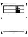
1
[00]COVER.fm 1 ページ
2004年11月12日 金曜日 午後2時22分
CODE : 00ZARFX11/A1E
LASER PRINTER OPTIONS
FAX EXPANSION KIT
(For U.S,A., Canada,
U.Kingdom, German, France)
MODEL
AR-FX11
OPTION
AR-MM9
CONTENTS
[1]
PRODUCT OUTLINE . . . . . . . . . . . . . . . . . . . . . . . . . . . . . . . . 1 - 1
[2]
CONFIGURATION . . . . . . . . . . . . . . . . . . . . . . . . . . . . . . . . . . 1 - 1
[3]
SPECIFICATIONS . . . . . . . . . . . . . . . . . . . . . . . . . . . . . . . . . . 3 - 1
[4]
EXTERNAL VIEWS AND INTERNAL STRUCTURES . . . . . . . 4 - 1
[5]
UNPACKING AND INSTALLATION. . . . . . . . . . . . . . . . . . . . . . 5 - 1
[6]
SIMULATIONS, FAX SOFTWARE SWITCH. . . . . . . . . . . . . . . 6 - 1
[7]
KEY OPERATOR PROGRAM . . . . . . . . . . . . . . . . . . . . . . . . . 7 - 1
[8]
TROUBLE CODE LIST. . . . . . . . . . . . . . . . . . . . . . . . . . . . . . . 8 - 1
[9]
ELECTRICAL SECTION . . . . . . . . . . . . . . . . . . . . . . . . . . . . . 9 - 1
Parts marked with “ “ are important for maintaining the safety of the set.
Be sure to replace these parts with specified ones for maintaining the safety and performance of the set.
SHARP CORPORATION
This document has been published to be used for
after sales service only.
The contents are subject to change without notice.
[co]CONTENTS.fm
1 ページ
2004年11月12日 金曜日 午後2時26分
CONTENTS
[1] PRODUCT OUTLINE . . . . . . . . . . . . . . . . . . . . . . . . . . . . 1-1
[6] SIMULATIONS, FAX SOFTWARE SWITCH
1. Entering the simulation mode . . . . . . . . . . . . . . . . . . . . 6-1
[2] CONFIGURATION . . . . . . . . . . . . . . . . . . . . . . . . . . . . . . 1-1
2. Canceling the simulation mode . . . . . . . . . . . . . . . . . . . 6-1
3. Simulation list . . . . . . . . . . . . . . . . . . . . . . . . . . . . . . . . 6-1
4. Detail of simulations . . . . . . . . . . . . . . . . . . . . . . . . . . . 6-2
[3] SPECIFICATIONS
5. FAX software switch . . . . . . . . . . . . . . . . . . . . . . . . . . . 6-22
1. FAX function specification . . . . . . . . . . . . . . . . . . . . . . 3-1
[7] KEY OPERATOR PROGRAM . . . . . . . . . . . . . . . . . . . . . . 7-1
[4] EXTERNAL VIEWS AND INTERNAL STRUCTURES
1. Operation panel . . . . . . . . . . . . . . . . . . . . . . . . . . . . . . 4-1
2. FAX mode (base screen) . . . . . . . . . . . . . . . . . . . . . . . 4-3
3. PWB . . . . . . . . . . . . . . . . . . . . . . . . . . . . . . . . . . . . . . . 4-4
[8] TROUBLE CODE LIST
1.FAX-related service call error. . . . . . . . . . . . . . . . . . . . . 8-1
2.Communication report codes . . . . . . . . . . . . . . . . . . . . . 8-1
[5] UNPACKING AND INSTALLATION . . . . . . . . . . . . . . . . . 5-1
[9] ELECTRICAL SECTION
1. FAX Block diagram . . . . . . . . . . . . . . . . . . . . . . . . . . . . 9-1
2. FAX Circuit diagram . . . . . . . . . . . . . . . . . . . . . . . . . . . 9-2
[01]OUTLINE ・ CONFIGU.fm
1 ページ 2004年11月12日 金曜日 午後2時22分
[1] PRODUCT OUTLINE
This unit provides the FAX function and the PC-FAX function when installed to the following machines:
Machines to install this unit :
• AR-M207
• AR-M165
• AR-M162
[2] CONFIGURATION
Extended memory
<AR-MM9>
* Installed to FAX MAIN PWB.
FAX Expansion Unit:1
FAX Keyboard:1
<AR-FX11>
AR-FX11 PRODUCT OUTLINE • CONFIGURATION 1-1
[03]SPECIFICATIONS.fm
1 ページ
2004年11月16日 火曜日 午前9時11分
[3] SPECIFICATIONS
Transmit function
1. Fax Function Specification
(1) Original
Original stack capacity 40 sheets.
Scan cycle
23opm.
Receive function
(2) Compression Method
MH, MR, MMR, JBIG.
(3) Image Process
Half tone reproduction Equivalent to 256 levels.
Exposure adjustment Auto and Manual (5 steps).
Resolution
STANDARD (8dot/mm x 3.85line/mm).
FINE (8dot/mm x 7.7line/mm).
SUPER FINE (8dot/mm x 15.4line/mm).
ULTRA FINE (16dot/mm x 15.4line/mm).
(4) Specified Destination
Specified destination
Rapid keys(Max.
number of keys to be
stored)
Speed
Program
Manual destination
entry
Chain dialing
Redial
Speed dialing
Specified by Dial, Rapid, Speed or Group
destination entry.
50 destinations (including Group).
300.
Yes (9).
Input via the numeric keys.
Yes (Pause Key).
The number last entered through the only
single address sending is stored (Except time
setting, Sub address and Passcode).
This is used to recall address control number
by using numeric keys.
Special function
(5) Specified Multiple Destinations
Specified destination
Broadcast
transmission
Sequential
broadcasting
Multi-polling
Specified by Rapid, Group, Speed or manual
destination entry (Broadcasting is not allowed
when sub address is registered).
Yes(F code inputting from ten key is excepted
in the address containing F code).
Yes (200 destinations).
Yes.
(6) Functions
Transmit function
Memory transmit
Speaker
Quick online
transmit
Direct transmit
Manual transmit
R-Key
Yes.
Yes.
Yes.
Report/List
function
Yes.
With speaker.
Speaker Key is set to R-Key
(Only for SEEG).
Auto reduction
Yes(Original is reduced and
transmit
sent according to the receivingside machine).
Rotation transmit Yes.
Scaling transmit Yes (Scaling from regular size
to regular size only. No rotation
enlargement allowed).
Recall Error
Yes.
mode
Busy
Yes.
Number of times/interval is set
via Key operator program.
Book original
Yes.
transmit
Long length
Yes.
original transmit Max.800m.
Verification stamp No.
AR-FX11 SPECIFICATIONS 3-1
Maximum number
of sender
registered
Maximum number
of transmission
reserved
Auto receive
Manual receive
Memory receive
Reduction receive
for standard size
Rotation receive
Divided receive
Duplex receive
2 in 1 receive
Only designated
number receiving
enabled
Enter junk fax
number
External phone
connection
Answering phone
connection
Transfer function
at output trouble
Auto startup
mode
Time setting
Transmit request
Remote transmit
Cover function
Print at sender
1 sender.
50 jobs.
Yes.
Yes.
Yes.
Yes.
Yes.
Yes: To be defined by Key
operator program.
Yes.
No.
No.
Yes (Up to 50numbers,
20digits).
Yes.
No (To avoid patent
infringement).
Yes.
No.
Yes.
Yes.
Yes.
Yes.
Yes (Always ON) (On/Off is
possible to set only for Japan).
Page division
Yes.
Page combination No.
Confidential
Yes (F code method).
(machine at the
other end)
Relay broadcast Yes (F code method).
direction
Transmit
Yes.
message
Edge erase
No.
Center erase
No.
Multi shot
No.
Card shot
No.
Confidential
Yes.
receive check list
Program list
Yes.
Relay group list
No.
ID sender list
No.
Transmit/receive Yes.
record
Reserved
Yes.
transmit list
Original storage Yes.
check list
Rapid dial list
Yes.
Speed dial list
Yes.
Group dial list
Yes.
Phone directory Yes.
list
Key operator
Yes.
program list
Confidential ID list No.
F-code setting
Yes.
check list
Account number No.
list
[03]SPECIFICATIONS.fm
2 ページ
Report/List
function
Others
2004年11月16日 火曜日 午前9時11分
Account control
record
Enter junk fax
number list
Transaction report
Confidential
registration list
Transmission
cancel list
Account control
Yes.
Yes.
Yes.
Yes.
Yes.
50 accounts.
(7) Transmission Method
Transmission time
Modem speed
Intercommunication
Communicationline
ECM
R-Key
2 seconds (level: Super G3 /33600bps).
6 seconds (G3 ECM/14400bps).
33.6kbps -> 2.4kbps automatic fallback
Super G3 / G3.
General telephone line (PSTN), Private branch
(PBX), Fax line.
Yes.
Available only for SEEG (with PBX setting).
(8) Record Size
Max. record width
Record size
293mm.
A3 - A5 (depends on destination).
11” x 17” - 5.5” x 8.5” (depends on destination).
(9) F-Code Transmission
Sub address
Passcode
Yes.
Yes.
(10)Other FAX Related Function/Remarks
FAST system support
PSTN supporting FAST
- SEC only
AR-FX11 SPECIFICATIONS 3-2
[04]ETERNALVIEWS.fm 1 ページ
2004年11月12日 金曜日 午後2時23分
[4] EXTERNAL VIEWS AND INTERNAL STRUCTURES
1. Operation panel
1
26
27
28
29
41
30
42
43
44
45
COPY
A
31
B
32
F
36
G
37
K
C
33
H
38
L
D
34
I
39
M
E
J
40
N
P
46
35
Q
47
U
R
V
SHIFT
T
49
W
SPEAKER REDIAL/PAUSE
O
S
48
50
XYZ
SP
SPEED
COMM. SETTING
SYMBOL
SPACE/–
ON LINE DATA
PRINT
SCAN
LINE
DATA
FAX
9
1
2
3
4
5
6
7
Page pallet
Display
[BACK] key
[FAX STATUS] key
[OK] key
Numeric keys
[C] key
8 [CA] key
9 [SPEAKER/SHIFT]
key
10 [REDIAL/PAUSE] key
11 [SPEED/SYMBOL]
key
12 [COMM. SETTING/
SPACE/-] key
13 Information lamp
10
11
12
13
14
15
These are used in fax mode.
This key displays the base screen and the function setting screen.
In a setting or programming screen, this key is used to move back to the previous screen.
This is used to cancel a fax transmission or a stored fax transmission.
This key is used to enter a setting that has been selected with the arrow or other keys.
These are used to enter fax numbers, sub-addresses, passcodes, and numerical settings.
This is used to clear a mistake when entering fax numbers, sub-addresses, passcodes, and numerical settings. One digit
is cleared each time the key is pressed.When an original is being scanned, this key can also be used to cancel scanning.
This is used to cancel a transmission or programming operation. When pressed during an operation, the operation is
canceled and the display returns to the base screen described on page *4 - 3*.This key is also used to cancel a resolution,
paper size, or special function setting that was selected when sending a fax.
This is used to dial without lifting the handset and to shift between upper and lower case when entering characters.
This is used to redial the last number dialed, and enter a pause when entering a fax number.
This is used to dial by Speed dialing and to enter a symbol when entering characters.
This is used to switch between memory transmission and direct transmission, and to switch between automatic reception
and manual reception. It is also used to enter a space or "-" when entering characters.
Information lamp blinks, when facsimile is received, or when the paper remains in the tray.
AR-FX11 EXTERNAL VIEWS AND INTERNAL STRUCTURES 4-1
[04]ETERNALVIEWS.fm 2 ページ
2004年11月12日 金曜日 午後2時23分
For U.S.A.
2
3
4
5
6
7
8
FAX STATUS
BACK
COPY EXPOSURE
PAPER
ZOOM
OK
ABC
DEF
GHI
JKL
MNO
PQRS
TUV
WXYZ
AUTO % OUTPUT DUPLEX
@.-_
SPECIAL FUNCTION
SCAN COLOR MODE RESOLUTION ADDRESS FORMAT ORIGINAL SIZE DUPLEX SCAN
FAX PROGRAM RESOLUTION ADDRESS BROADCAST ORIGINAL SIZE DUPLEX SCAN
16
17
18
19
20
21
ACC. #-C
23
22
READ-END
25
26 24
For other country
2
3
4
5
6
7
8
FAX STATUS
BACK
PAPER
COPY EXPOSURE SELECT
COPY
RATIO
AUTO
IMAGE
OUTPUT
2-SIDED
COPY
OK
14 [MODE SELECT] keys
15 [FAX] key/
FAX indicator/LINE
indicator/DATA
indicator
16 [PROGRAM] key
17 [RESOLUTION] key
18 [ADDRESS] key
19 [BROADCAST] key
20 [ORIGINAL SIZE] key
21 [DUPLEX SCAN] key
22 [SPECIAL
FUNCTION] key
23 Arrow keys
24 [START] key
25 [ACC.#-C] key
26 [READ-END] key
17
18
19
20
21
DEF
GHI
JKL
MNO
PQRS
TUV
WXYZ
@.-_
SPECIAL FUNCTION
SCAN COLOUR MODE
FORMAT
RESOLUTION ADDRESS
ORIGINAL SIZE DUPLEX SCAN
FAX PROGRAM
BROADCAST
16
ABC
23
ACC. #-C
22
READ-END
25
26 24
These are used these keys to change modes.
Press to switch to fax mode. The base screen of fax mode will appear in the display. The LINE indicator lights up during
transmission or reception of a fax. When a fax has been received, the DATA indicator blinks. (When there is fax
transmission data in memory, the DATA indicator lights up.)
Press this key to use a program.
This key is used to select resolution and exposure settings.
This key is used to search for a fax destination that has been stored as an auto-dial number in the address book.
This is used to perform a broadcast transmission.
This is used to set the size of the original to be faxed.
Press this key to use the duplex scan function. (Only on models with a SPF installed.)
This key is used to select a special transmission or reception function, configure function settings, and to store auto-dial
numbers.
These are used to select items and move through pages.
This is used at the following times:
(1) When starting transmission
(2) When scanning an original
(3) When starting manual reception
(4) When configuring and storing settings
Press the end the use of an account and return the display to the account number entry screen.
When copying in sort mode from the document glass, press this key when you have finished scanning the original pages
and are ready to start copying.
NOTE
• When the auto power shut-off function is activated, All lights except the mode key lights go off. For the information on the auto power shut-off function.
AR-FX11 EXTERNAL VIEWS AND INTERNAL STRUCTURES 4-2
[04]ETERNALVIEWS.fm 3 ページ
2004年11月12日 金曜日 午後2時23分
2. FAX mode (base screen)
The base screen of fax mode is displayed by pressing the [FAX] key when the print mode, copy mode, or scan mode
screen appears.
A. The base screen of fax mode
1
2
3
4
5
1
Message display
2
3
Date and time display
Transmission mode display
4
5
6
7
Exposure display
Resolution display
Free memory display
Reception mode display
8
Original display
Stand-by.
96%
MAY 10 MON 10:25 AM
MEMORY
AUTO
CONT AUTO
812 x11R
STANDARD
6
7
8
Messages appear here to indicate the current status of the machine. An icon appears to the right side when a
confidential fax has been received.
This shows the date and time.
There are three transmission modes: memory transmission, direct transmission, and manual transmission.
This shows the currently selected transmission mode.
This shows the exposure for scanning the original that has been selected with the [RESOLUTION] key.
This shows the resolution for scanning the original that has been selected with the [RESOLUTION] key.
This shows the percentage of fax memory that is free.
There are two modes for receiving faxes:
automatic reception and manual reception. This shows the currently selected reception mode.
This displays an icon to indicate the original scanning mode when an original has been placed.
: One-sided original scanning in the SPF.
: Document glass.
: Two-sided original scanning in the RSPF.
This also shows the size of the placed original.
NOTE
The following functions operate even when copy mode is selected:
• Automatic reception (including F-code confidential reception)
• Timer Transmission
• Memory polled function
• Transmission of stored memory transmission jobs
• Voice calls (voice calls can be answered but not placed).
• Remote reception
• Manual reception
• Relay station function for F-code relay broadcast transmission
AR-FX11 EXTERNAL VIEWS AND INTERNAL STRUCTURES 4-3
[04]ETERNALVIEWS.fm 4 ページ
2004年11月12日 金曜日 午後2時23分
3. PWB
2
4
3
1
1
2
3
4
FAX control PWB
FAX FLASH ROM PWB
TEL/LIU PWB
FAX extended memory
(Installed to FAX control PWB)
FAX communication control
FAX control program
TEL line communication control
<AR-MM9>
AR-FX11 EXTERNAL VIEWS AND INTERNAL STRUCTURES 4-4
[05]UNPACKINGANDINSTALLATION.fm
1 ページ
2004年11月12日 金曜日 午後2時23分
[5] UNPACKING AND INSTALLATION
<Before installation>
• For improvement of workability, some description in this manual as well
as components and accessories may change without prior notice.
In this case, refer to the service manual.
2) Work the rear cover.
Cut and remove the cut-out portion from the rear cover using a tool
such as nippers. Be careful with the tool's direction so that the cut
surface would be flat.
Parts included
line cable: 1
FAX Expansion Unit: 1
Screws (S tight): 4
Writing label: 4
FAX keyboard: 1
FCC label: 1
(USA, Canada only)
Installation Manual: 1
Installing additional memory board (AR-MM9)
* If no need to install, go on to Step 3 to continue FAX Expansion Kit
Installation.
Insert an additional memory board into the socket of FAX Expansion
Unit. Be careful with the inserting direction. Make sure that it is securely
inserted.
Operation manual: 1
Turn off the main switch of the copier and then remove the power plug
of the copier from the outlet.
1) Detach the rear cover.
<1>Unscrew two screws from the rear cover.
<2>Push to release the lock shown in the illustration below. Slide to right
and remove the rear cover.
3) Install FAX Expansion Unit.
<1>Hook the attaching parts of FAX Expansion Unit (two on the right)
onto the copier frame as shown.
<2>Hook the attaching part of FAX Expansion Unit (one on the left) onto
the copier frame as shown.
<3>Push the lower left side of the unit to make sure that connectors of
FAX Expansion Unit and the copier are connected.
<4>Secure the unit onto the copier using four supplied screws (S tight)
as shown.<1>Hook the attaching parts of FAX Expansion Unit (two
on the right) onto the copier frame as shown.
AR-FX11 UNPACKING AND INSTALLATION 5-1
[05]UNPACKINGANDINSTALLATION.fm
2 ページ
2004年11月12日 金曜日 午後2時23分
4) Reattach the rear cover.
<1>Insert the claw locks of the rear cover into the copier, and slide it to
left until they are securely locked.
<2>Secure the cover using two screws.
5) Remove keyboard back cover.
<1>Unscrew two screws from the keyboard back cover.
<2>Release the lock as shown, and remove the back cover.
8) Reattach keyboard back cover.
<1>Insert the claw lock of the keyboard back cover into the copier. Make
sure that the claw lock is securely inserted.
<2>Secure the cover using two screws.
9) Paste FCC label on the rear cabinet of the copier.
After installing FAX Expansion Kit, paste the supplied FCC label on
the position shown in the illustration.
USA, Canada only
In order to manifest the compliance with FCC Part 68 and IC CS-03, it
is required to provide the machine with the FCC Registration Number
(USA), Ringer Equivalence (USA) and Ringer Eqivalence(Canada).
After installing the FAX expansion kit in the machine, please put the
registration label, packed with the kit, on the prescribed location.
6) Remove dummy panel.
<1>Unscrew from the dummy panel.
<2>Push the dummy panel up using a driver as shown, and remove it
from the copier.
Insert the power plug of the copier to the outlet, and then turn on the
main switch of the copier.
10) Setup date and time.
Press [FUNCTION] key on the Operation Panel, select [Key Operator
Program], enter 5-digit key operator code, and select [FAX] mode.
Select [Initial setup] and then [Date and Time]. Enter date in the
order of year, Month, Day and press [OK] to set.
Select [Time Setup], enter time in the order of Hour and Minute, and
press [OK] to set.
7) Attach FAX keyboard.
<1>Connect the copier flat cable to FAX keyboard.
<2>Place the FAX keyboard onto the copier.
<3>Secure the keyboard using a screw.
11) Clear image memory.
* When additional memory board (AR-MM9) is installed, you must clear
the memory using the Simulation [66-10]. If no additional memory is
installed, there is no need for this memory clear process.
12) Connect line cable.
Connect the line cable to the FAX Expansion Kit.
AR-FX11 UNPACKING AND INSTALLATION 5-2
[06]SIMULATIONS ・ FAXSOFTWARESWITCH.fm
1 ページ
2004年11月12日 金曜日 午後2時24分
[6] SIMULATIONS, FAX SOFTWARE SWITCH
1. Entering the simulation mode
Perform the following procedure to enter the simulation mode.
[#]
[*]
[C]
[*]
[Main code]
[START]
[Sub code]
[START]
2. Canceling the simulation mode
When the clear all key is pressed, the simulation mode is cancelled.
When the interruption key is pressed, the process is interrupted and the
screen returns to the sub code entering display.
* After canceling the simulation mode, be sure to turn OFF/ON the
power and check the operation.
Note:
• If the machine is terminated by a jam error or paper empty during
copying in the adjustment by the simulation, recopying is required.
• The values in the simulation columns are not default values but sample
values.
3. Simulation list
CODE
FUNCTION(Contents)
MAIN
SUB
22
11
FAX-related counter display
24
10
FAX-related counter clear
46
12
Density adjustment in the FAX mode
(Collective adjustments)
13-16
Density adjustment in the FAX mode
(Individual adjustments)
48
50
66
39
FAX sharpness adjustment
8
FAX magnification ratio adjustment
(scan)
9
FAX magnification ratio adjustment
(print)
8
FAX lead edge adjustment (scan)
9
FAX lead edge adjustment (print)
1
FAX soft SW setting
2
FAX soft SW initializing
3
FAX PWB memory check
4
Signal send mode
6
Print pass code print
7
Image memory content print
10
Image memory contents clear
11
300bps signal send
13
Dial test
17
DTMF signal send
19
SRAM backup
21
FAX information print
24
FAST SRAM clear
30
TEL/LIU status change check
31
TEL/LIU setting
32
Receive data check
33
Signal detection check
34
Communication time measurement
37
Speaker sound volume adjustment
38
Time setting/check
41
CI signal check
52
Pseudo ringer check
AR-FX11 SIMULATIONS, FAX SOFTWARE SWITCH 6-1
[06]SIMULATIONS ・ FAXSOFTWARESWITCH.fm 2 ページ
2004年11月12日 金曜日 午後2時24分
4. Detail of simulations
Main
code
Sub
code
22
11
Contents
FAX-related counter display.
Used to display the current FAX send/receive counter value.
Sim22-11 FAX COUN.
SELECT COUNTER
1:COMM. PAGE
2:COMM. TIME
(1 - 3)
Sim22-11 FAX COUN.
SELECT COUNTER
3:PRINT PAGE
1
2
3
OK
OK
OK
Sim22-11 FAX COUN.
COMM. TIME
SND:hhhhhhhh:mm:ss
RCV:hhhhhhhh:mm:ss
Return
10
CA key
: Simulation cancel
Interrupt key : Sub code input window
(1 - 3)
Sim22-11 FAX COUN.
COMM. PAGE
SND xx, xxx, xxx
RCV xx, xxx, xxx
24
Remark
Sim22-11 FAX COUN.
PRINT PAGE
xxxxxxxx
Return
FAX-related counter clear
Used to clear the current FAX send/receive counter value (number of pages of send/receive), the
accumulated time of send/receive, and the print counter to 0.
Sim24-10 CLR COUN.
CLEAR FAX COUNTER
1:SEND
2:RECEIVE
(1 - 3)
X
Sim24-10 CLR COUN.
CLEAR FAX COUNTER
3:PRINT PAGE
(1 - 3)
X
CA key
: Simulation cancel
Interrupt key : Sub code input window
1
2
3
OK
OK
OK
Sim24-10 CLR COUN.
SEND
PAGE: xx, xxx, xxx
TIME: hhhhhhhh:mm:ss
EXEC
OK
Sim24-10 CLR COUN.
SEND COUN. CLEARED
Return
Sim24-10 CLR COUN.
RECEIVE
PAGE: xx, xxx, xxx
TIME: hhhhhhhh:mm:ss
EXEC
Sim24-10 CLR COUN.
PRINT PAGE
xxxxxxxx
EXEC
OK
OK
Sim24-10 CLR COUN.
RCV COUN. CLEARED
Sim24-10 CLR COUN.
FAX COUN. CLEARED
Return
When the number of pages of send is cleared, the PC-FAX counter is also cleared.
AR-FX11 SIMULATIONS, FAX SOFTWARE SWITCH 6-2
Return
[06]SIMULATIONS ・ FAXSOFTWARESWITCH.fm 3 ページ
Main
code
Sub
code
46
12
2004年11月12日 金曜日 午後2時24分
Contents
Density adjustment in the FAX mode (Collective adjustments)
Used to adjust the density in the FAX mode to “AUTO” or “0” - “99”.
Sim46-12 EXP LEVEL
AUTO
XX
( 0 - 99 )
YY
After input
0 - 99
OK
Sim46-12 EXP LEVEL
AUTO
YY
EXEC
Sim46-12 EXP LEVEL
AUTO
YY
SCAN
EXEC
Sim46-12 EXP LEVEL
AUTO
YY
PRINT
EXEC
AR-FX11 SIMULATIONS, FAX SOFTWARE SWITCH 6-3
Remark
[06]SIMULATIONS ・ FAXSOFTWARESWITCH.fm 4 ページ
Main
code
Sub
code
46
13-16
2004年11月12日 金曜日 午後2時24分
Contents
Remark
Density adjustment in the FAX mode (Individual adjustments)
Used to adjust the density in the FAX mode to “AUTO” or “0” - “99”.
Sim46-13 EXP LEVEL
STD.
1:AE
2:MANUAL
(1-2)
Sim46-14 EXP LEVEL
X
After input 1 - 2
OK
After input 1 - 4
OK
Sim46-13 EXP LEVEL
STD.
AE
(2DIGITS)
Sim46-14 EXP LEVEL
XX
FINE
AE PHOTO ON
XX
YY
(2DIGITS)
YY
After input 0 - 99
After input 0 - 99
OK
OK
Sim46-13 EXP LEVEL
STD.
AE
Sim46-14 EXP LEVEL
YY
FINE
AE PHOTO ON
EXEC
STD.
AE
Sim46-14 EXP LEVEL
YY
FINE
AE PHOTO ON
EXEC
SCAN
Sim46-13 EXP LEVEL
STD.
AE
PRINT
Sim46-15
S-FINE
3:MANUAL(PHOTO ON)
4:MANUAL(PHOTO OFF)
)
X
(1
S-FINE
1:AE(PHOTO ON)
2:AE(PHOTO OFF)
)
X
(1
YY
EXEC
Sim46-16
Sim46-16
U-FINE
1:AE(PHOTO ON)
2:AE(PHOTO OFF)
)
X
(1
After input 1 - 4
After input 1 - 4
Sim46-15
EXEC
FINE
AE PHOTO ON
EXEC
Sim46-15
YY
Sim46-14 EXP LEVEL
YY
PRINT
YY
EXEC
Sim46-13 EXP LEVEL
SCAN
Sim46-14 EXP LEVEL
FINE
3:MANUAL(PHOTO ON)
4:MANUAL(PHOTO OFF)
X
(1 4)
FINE
1:AE(PHOTO ON)
2:AE(PHOTO OFF)
X
(1 4)
Sim46-16
S-FINE
AE PHOTO ON
XX
U-FINE
AE PHOTO ON
XX
(2DIGITS)
YY
(2DIGITS)
YY
After input 0 - 99
After input 0 - 99
Sim46-15
Sim46-16
S-FINE
AE PHOTO ON
YY
U-FINE
AE PHOTO ON
EXEC
Sim46-15
YY
EXEC
Sim46-16
S-FINE
AE PHOTO ON
YY
U-FINE
AE PHOTO ON
YY
SCAN
EXEC
SCAN
EXEC
Sim46-15
Sim46-16
S-FINE
AE PHOTO ON
YY
U-FINE
AE PHOTO ON
YY
PRINT
EXEC
PRINT
EXEC
AR-FX11 SIMULATIONS, FAX SOFTWARE SWITCH 6-4
U-FINE
3:MANUAL(PHOTO ON)
4:MANUAL(PHOTO OFF)
)
X
(1
[06]SIMULATIONS ・ FAXSOFTWARESWITCH.fm 5 ページ
Main
code
Sub
code
46
39
2004年11月12日 金曜日 午後2時24分
Contents
Remark
FAX sharpness adjustment
Used to adjust the resolution and the filer in the FAX mode.
Sim46-39 FAX IMAGE
1:STD.
2:FINE
3:S-FINE
(1 - 7 )
Return
Sim46-39 FAX IMAGE
4:U-FINE
5:FINE/HT
6:S-FINE/HT
(1 - 7 )
1
1
1
X
1
1
1
X
Sim46-39 FAX IMAGE
7:U-FINE/HT
1
(1 - 7 )
X
The current set value of each resolution is displayed.
1 - 7 input
OK
Specify a resolution to be set.
Sim46-39 FAX IMAGE
STD.
X
(0 - 2 )
Y
0 - 2 input
Return
OK
Specify the kind of a filter to be set.
Sim46-39 FAX IMAGE
STD.
Y
EXEC
OK
Self print operation is executed. (The specified kind of the filter is used.)
The specified filter is used even in the normal operation.
Sim46-39 FAX IMAGE
STD.
Y
SCAN
EXEC
Scanning operation
Sim46-39 FAX IMAGE
STD.
Y
PRINT
EXEC
Printing operation
* When "Interrupt" key is pressed on a window other than the operation window,
the display shifts to the sub code input window.
AR-FX11 SIMULATIONS, FAX SOFTWARE SWITCH 6-5
[06]SIMULATIONS ・ FAXSOFTWARESWITCH.fm 6 ページ
Main
code
Sub
code
48
8
2004年11月12日 金曜日 午後2時24分
Contents
FAX magnification ratio adjustment (scan)
Used to adjust and set the FAX document scan magnification ratio and scan and print the document.
Sim48-8
1:OC
2:SPF
3:RSPF
(1-3)
SCAN RATIO
X
After input
1-3
OK
Sim48-8 SCAN RATIO
OC
1:MAIN SCAN RATIO XXX
2:SUB SCAN RATIO XXX
(1-2)
X
After input
1-2
OK
Sim48-8 SCAN RATIO
OC MAIN SCAN RATIO XXX
( 1 - 255 )
YYY
After input
1 - 255
OK
Sim48-8
SCAN RATIO
OC MAIN SCAN RATIO XXX
EXEC
Sim48-8
SCAN RATIO
OC MAIN SCAN RATIO YYY
SCAN
Sim48-8
EXEC
SCAN RATIO
OC MAIN SCAN RATIO YYY
PRINT
EXEC
AR-FX11 SIMULATIONS, FAX SOFTWARE SWITCH 6-6
Remark
[06]SIMULATIONS ・ FAXSOFTWARESWITCH.fm 7 ページ
Main
code
Sub
code
48
9
2004年11月12日 金曜日 午後2時24分
Contents
Remark
FAX magnification ratio adjustment (print)
Used to adjust and set the FAX print magnification ratio and scan and print the document.
Sim48-9
PRI. RATIO
1:MAIN SCAN RATIO XXX
2:SUB SCAN RATIO XXX
3:MAIN SCAN/R XXX
(1-4)
X
Sim48-9
PRI. RATIO
4:SUB SCAN/R XXX
(1-4)
X
After input
1-4
OK
Sim48-9
PRI. RATIO
MAIN SCAN/R
XXX
( 1 - 255)
YYY
After input
1 - 255
OK
Sim48-9
PRI. RATIO
MAIN SCAN/R
YYY
EXEC
Sim48-9
PRI. RATIO
MAIN SCAN/R
YYY
SCAN
EXEC
Sim48-9
PRI. RATIO
MAIN SCAN/R
YYY
PRINT
EXEC
AR-FX11 SIMULATIONS, FAX SOFTWARE SWITCH 6-7
[06]SIMULATIONS ・ FAXSOFTWARESWITCH.fm 8 ページ
Main
code
Sub
code
50
8
2004年11月12日 金曜日 午後2時24分
Contents
Remark
FAX lead edge adjustment (scan)
Used to adjust and set the FAX document scan lead edge position and scan and print the document.
Sim50-8
1:OC
2:SPF
3:RSPF
(1-3)
SCAN EDGE
X
After input
1-3
OK
Sim50-8 SCAN EDGE
OC
1:LEAD EDGE
XX
2:LEFT EDGE
XX
(1-4)
X
Sim50-8
SCAN EDGE
OC
3:REAR EDGE XX
4:RIGHT EDGS XX
(1-4)
X
After input
1-4
OK
Sim50-8 SCAN EDGE
OC LEAD EDGE XX
( 43- 57 )
YY
After input
43 - 57
OK
Sim50-8
SCAN EDGE
OC LEAD EDGE XX
EXEC
Sim50-8
SCAN EDGE
OC LEAD EDGE XX
SCAN
Sim50-8
EXEC
SCAN EDGE
OC LEAD EDGE XX
PRINT
EXEC
AR-FX11 SIMULATIONS, FAX SOFTWARE SWITCH 6-8
[06]SIMULATIONS ・ FAXSOFTWARESWITCH.fm 9 ページ
Main
code
Sub
code
50
9
2004年11月12日 金曜日 午後2時24分
Contents
Remark
FAX lead edge adjustment (print)
Used to adjust and set the FAX print lead edge position and scan and print the document.
Sim50-9
PRINT EDGE
1:LEAD EDGE
2:LEFT EDGE
3:REAR EDGE
( 1 - 6)
XX
XX
XX
X
Sim50-9
PRINT EDGE
4:LEAD EDGE/R XX
5:LEFT EDGE/R XX
6:REAR EDGE/R XX
( 1 -6 )
X
After input
1-6
OK
Sim50-9
PRINT EDGE
LEAD EDGE/R
XX
( 43- 57)
YY
After input
43 - 57
OK
Sim50-9
PRINT EDGE
LEAD EDGE/R
XX
EXEC
Sim50-9
XX
SCAN
EXEC
Sim50-9
66
1
PRINT EDGE
LEAD EDGE/R
PRINT EDGE
LEAD EDGE/R
XX
PRINT
EXEC
FAX soft SW setting
Used to display the FAX-related soft SW on the LCD and set and change the soft SW setting with 10-key
input.
Sim66-1 FAX SOFT SW
ENTER FAX SOFT SW.#
( 3DIGITS )
XXX
OK
XXX is the input value of the soft SW number.
Sim66-1 FAX SOFT SW
No.XXX
XXXXXXXX
USE # KEY 12345678
OK
Sim66-1 FAX SOFT SW
No.XXX XXXXXXXX
CA key
: Simulation cancel
Interrupt key : Sub code input window
10-key
: Soft SW input
bit No. input
OK key
: Settlement of the input value
START key : Settlement of the input value
C key
: Input number clear for soft SW number input,
disable for the following windows
1sec later
To the initial window of SIM66-1
AR-FX11 SIMULATIONS, FAX SOFTWARE SWITCH 6-9
[06]SIMULATIONS ・ FAXSOFTWARESWITCH.fm
Main
code
Sub
code
66
2
10 ページ 2004年11月12日 金曜日 午後2時24分
Contents
Remark
FAX soft SW initializing
Used to clear the FAX-related soft SW values except for the line signal adjustment value and the machine
adjustment value and set them to the default values (which differ depending on the country code).
Sim66-2 SOFT SW
Sim66-2 SOFT SW
COUNTRY CODE
Japan
00000000
COUNTRY CODE
Sweden
10100101
1/26 SELECT UP DN
26/26 SELECT UP DN
Input of a value cannot be made.
OK
Sim66-2 SOFT SW COUNTRY CODE
INITIAL
ARE YOU SURE? EXEC
OK
Sim66-2 SOFT SW COUNTRY CODE
INITIAL
EXEC
Completion of execution
(Highlighted during execution)
Sim66-2 SOFT SW COUNTRY CODE
INITIALIZED
Selection
Japan
U.S.A.
U.K.
China
India
Taiwan
Australia
New Zealand
Singapore
Malaysia
Hong Kong
Middle east
Germany
France
Spain
Portugal
Denmark
Norway
Switzerland
Italy
Belgium
Luxembourg
Netherlands
Finland
Sweden
00000000
10110101
10110100
00100110
01010011
11111110
00001001
01111110
10011100
01101100
01010000
11111101
00000100
00111101
10100000
10001011
00110001
10000010
10100110
01011001
00001111
01101001
01111011
00111100
10100101
CA key
: Simulation cancel
Interrupt key : Sub code input window
OK key
: Settlement
START key : Settlement
C key
: Disable
Return key : Disable
1sec later
Simulation code input window
3
FAX PWB memory check
Used to check read/write from/into the memory on the FAX PWB. The check result is displayed for each
memory.
Sim66-3
MEMOR CHK
1:DRAM 4:OPTION
2:SRAM 5:PAGE
3:FLASH 6:MODEM
(1-6)
X
CA key
Interrupt key
10-key
OK key
START key
Return key
C key
:
:
:
:
:
:
:
Simulation cancel
Sub code input window
Item selection
Settlement and execution of the input value
Settlement of the input value
Returns to the selection window.
Disable
OK
Sim66-3
MEMOR CHK
DRAM
EXEC
OK
Sim66-3
MEMOR CHK
DRAM
CHECKING MEMORY
*Interruption with C key during execution cannot be made.
EXEC
Execution normal end
(Highlighted during execution)
Sim66-3
MEMOR CHK
DRAM
MEMORY CHECK
RESULT
OK
Return
SIM66-3 initial window
Execution error end (Highlighted during execution)
Sim66-3
MEMOR CHK
DRAM
MEMORY CHECK
RESULT
NG XXXXXXXX SUM
NG
NG
NG
NG
NG
NG
XXXXXXXX SUM
XXXXXXXX A-BUS
XXXXXXXX DATA
XXXXXXXX D-BUS
XXXXXXXX ERASE
XXXXXXXX IO
Return
SIM66-3 initial window
AR-FX11 SIMULATIONS, FAX SOFTWARE SWITCH 6-10
[06]SIMULATIONS ・ FAXSOFTWARESWITCH.fm
Main
code
Sub
code
66
4
11 ページ 2004年11月12日 金曜日 午後2時24分
Contents
Remark
Signal send mode
Used to send signals to the line and the machine speaker by setting the signal number. (Signal send is
continued until interruption is instructed by pressing RETURN key.) The signal send level is selected from
0db and the soft SW values. Since the level setting is not required for 01 and 31 - 35, the selection menu
does not appear. The signal send level is returned to the soft SW set value before execution of the mode
when completing the mode.
CA key
:
Interrupt key :
C key
:
key
:
10-key
:
OK key
:
START key :
RETURN key :
Sim66-4 SIGNAL OUT
SIGNAL SELECT
(1 - 35)
Simulation cancel
Sub code input window
Input clear
Page select
Number input and item selection
Input value settlement and execution
Input value settlement
Signal send stop
1sec later
Sim66-4 SIGNAL OUT
Sim66-4 SIGNAL OUT
34:DP MAKE
35:DP BREAK
1:NO SIGNAL
2:33600bps(V34)
3:31200bps(V34)
(1 - 35)
XX
(1 - 35)
XX
After selection with 10-key
The window is switched with the up and down keys.
OK
Input and switching the window are irrelevant.
Not highlighted with an input of a value.
Sim66-4 SIGNAL OUT
The window is not switched, either.
33600bps(V34)
1:MAX
When "1: NO SIGNAL" or "31: PSEUDO RNG" - "33: R.B. TONE NONE"
2:SOFT SW.
is selected, "0dB" and "SOFT SW" are not selected.
(1 - 2)
X
When one of these is selected, the second line is the signal name,
the third and fourth lines are empty, and the fifth line is EXEC display.
OK
Sim66-4 SIGNAL OUT
33600bps(V34)
0dB
EXEC
After pressing OK key
OK
Sim66-4 SIGNAL OUT
33600bps(V34)
PRESS BACK TO STOP
EXEC
Return
SIM66-4 initial window
6
Print pass code print
Used to print the confidential ID table (confidential box number, confidential box name, confidential pass
code). Sharp mode confidential information is printed separately.
Sim66-6
PASS CODE
OK
PRINT CONF.
Sim66-6
PASS CODE
1sec later
PRINT STORED
OK
EXEC
OK
Sim66-6
Sim66-6
PASS CODE
NO DATA
1sec later
CA key
: Simulation cancel
Interrupt key : Sub code input
window
OK key
: Settlement
START key : Settlement
C key
: Disable
Return key : Disable
PASS CODE
CAN NOT PRINT
1sec later
AR-FX11 SIMULATIONS, FAX SOFTWARE SWITCH 6-11
[06]SIMULATIONS ・ FAXSOFTWARESWITCH.fm
12 ページ 2004年11月12日 金曜日 午後2時24分
Main
code
Sub
code
Contents
66
7
Image memory content print
Used to print all the image data (confidential receive contents, remote send images, and images which are
not sent yet) in the image memory of the FAX section. The printed images are remained in the memory after
printing.
OK
Sim66-7 PRINT MEMORY
Remark
Sim66-7 PRINT MEMORY 1sec later
PRINT STORED
PRINT IMAGE MEMORY
EXEC
OK
(When there is no image memory)
OK
Sim66-7 PRINT MEMORY
Sim66-7 PRINT MEMORY
NO DATA
1sec later
10
CA key
: Simulation cancel
Interrupt key : Sub code input
window
OK key
: Settlement
START key : Settlement
C key
: Disable
Return key : Disable
CAN NOT PRINT
1sec later
Image memory contents clear
Used to clear all the image data (including confidential receive contents) in the image memory of the FAX
section. The management table is also cleared (initialized) at the same time.
CA key
: Simulation cancel
Interrupt key : Sub code input
window
OK key
: Settlement
Return key : Simulation code input window
START key : Settlement
C key
: Disable
Sim66-10 IMAGE CLR
CLEAR IMAGE MEMORY
ARE YOU SURE? EXEC
After pressing OK key,
during execution
OK
Sim66-10 IMAGE CLR
CLEAR IMAGE MEMORY
Completion of execution
(Highlighted during execution)
EXEC
Completion of execution
(Highlighted during execution)
With prints
Sim66-10 IMAGE CLR
CLEARED IMAGE MEM.
DO POWER OFF
Power source OFF/ON
Without prints
Sim66-10 IMAGE CLR
CLEARED
Return
Simulation code input window
AR-FX11 SIMULATIONS, FAX SOFTWARE SWITCH 6-12
[06]SIMULATIONS ・ FAXSOFTWARESWITCH.fm
13 ページ 2004年11月12日 金曜日 午後2時24分
Main
code
Sub
code
Contents
66
11
300bps signal send
Used to send the specified signal at the speed of 300bps by setting the signal number. (Signal send is
continued until interruption is instructed by pressing RETURN key.) The signal send level is selected from
0db and soft switch set values. The signal send level is returned to the sot SW set value before execution of
the mode after completion of the mode.
Sim66-11 300bps SIG.
SIGNAL LEVEL
1:MAX
2:SOFT SW.
(1-2)
X
After selection
with 10-key
OK
CA key
Interrupt key
C key
keys
10-key
OK key
START key
RETURN key
Remark
:
:
:
:
:
:
:
:
Simulation cancel
Sub code input window
Input clear
Page switch
Item selection
Input value settlement and execution
Input value settlement
Signal send stop
Sim66-11 300bps SIG.
1:NO SIG.
2:11111
3:11110
(1-6)
4:00000
5:010101
6:00001
X
After selection
with 10-key
OK
Sim66-11 300bps SIG.
NO SIGNAL
EXEC
After pressing OK key,
during execution
OK
Sim66-11 300bps SIG.
OUTPUTING SIGNAL
PRESS BACK TO STOP
EXEC
Return
SIM66-11 initial window
AR-FX11 SIMULATIONS, FAX SOFTWARE SWITCH 6-13
[06]SIMULATIONS ・ FAXSOFTWARESWITCH.fm
14 ページ 2004年11月12日 金曜日 午後2時24分
Main
code
Sub
code
Contents
Remark
66
13
Dial test
Used to send the dial pulse and the DTMF signal, and perform the dial pulse make time adjustment and the
DTMF signal send level adjustment according to necessity.
Sim66-13 DIALTEST
1:PULSE 10pps
2:PULSE 20pps
3:DTMF
( 1-3 )
X
Select with 10-key and press OK key.
After selection
with 10-key
OK
Sim66-13 DIALTEST
PULSE 10pps
INPUT MAKE TIME
YY
( 26-41 )
YY
After selection
with 10-key
OK
Sim66-13 DIALTEST
PULSE 10pps
Yyms
INPUT DIAL #
XXXXXXXXXXXXX
EXEC
The input of 10-key enters the fourth digit.
(If there are too many, scroll to the left.)
Sim66-13 DIALTEST
SELECT HIGH LEVEL
1:DEFAULT
2:SOFT SW.
Y
( 1-2 )
X
After selection
with 10-key
OK
Sim66-13 DIALTEST
INPUT HIGH LEVEL
DTMF SOFT SW.
Y
( 0-21 )
XX
After selection
with 10-key
OK
Sim66-13 DIALTEST
Sim66-13 DIALTEST
SEND 10 pps
Yyms
INPUT DIAL #
XXXXXXXXXXXXX
EXEC
After pressing OK key,
during execution
OK
Sim66-13 DIALTEST
SENDING 10 pps Yyms
INPUT DIAL #
XXXXXXXXXXXX
EXEC
Completion of execution
(Highlighted during execution)
SIM66-13 initial window
CA key
Interrupt key
C key
10-key
:
:
:
:
OK key
START key
RETURN key
XXXXXXXX
:
:
:
:
Simulation cancel
Sub code input window
Input clear
Input of time and dial number
and selection of an item
Settlement and execution of an input
Settlement of an input
Returns to the selection window
Input dial
SELECT LOW LEVEL
1:DEFAULT
2:SOFT SW.
Y
( 1-2 )
X
When "1" is selected
OK
OK
When "2" is selected
Sim66-13 DIALTEST
INPUT LOW LEVEL
DTMF SOFT SW.
Y
( 0-15 )
XX
Select with 10-key
and press OK key.
OK
Sim66-13 DIALTEST
DTMF HIGH:XX LOW:YY
INPUT DIAL #
XXXXXXXXXXXXX
EXEC
After pressing OK key,
during execution
OK
Sim66-13 DIALTEST
DTMF HIGH:XX LOW:YY
INPUT DIAL #
XXXXXXXXXXXXX
EXEC
Completion of execution
(Highlighted during execution)
SIM66-13 initial window
AR-FX11 SIMULATIONS, FAX SOFTWARE SWITCH 6-14
[06]SIMULATIONS ・ FAXSOFTWARESWITCH.fm
15 ページ 2004年11月12日 金曜日 午後2時24分
Main
code
Sub
code
Contents
66
17
DTMF signal send
Used to select the signal send level from 0dB and the soft SW set values and specify a dial number to be
sent. The DTMF signal of the specified dial number is sent continuously until the interrupt command is made
by pressing RETURN key. When another dial number is specified during sending of the signal, the signal
send level is returned to the soft SW set value before execution of the mode after completion of the mode.
Sim66-17 DTMF SIG.
1:MAX
2:SOFT SW.
( 1-2 )
X
CA key
Interrupt key
C key
10-key
OK key
START key
RETURN key
:
:
:
:
:
:
:
Remark
Simulation cancel
Sub code input window
Input clear and stop
Item selection, dial number input
Input value settlement and execution
Input value settlement and execution
Signal send stop
After selection with 10-key
OK
Sim66-17 DTMF SIG.
INPUT DIAL #
X
EXEC
The 10-key input enters the third digit.
OK
Sim66-17 DTMF SIG.
SENDING SIGNAL
X
PRESS BACK TO STOP
EXEC
Completion of execution (Highlighted during execution)
Return
SIM66-17 initial window
19
SRAM backup
Used to back up and restore the SRAM contents.
Sim66-19
BACK UP
1:SRAM BACK UP
2:SRAM RESTORE
( 1-2 )
X
After inputting
1 or 2
After pressing OK key,
during execution
OK
Sim66-19
BACK UP
OK
Sim66-19
SRAM BACK UP
ARE YOU SURE?EXEC
After pressing OK key,
during execution
BACK UP
NO DATA
RETURN key
SIM66-19 initial window
OK
After pressing OK key,
during execution
OK
Sim66-19
Sim66-19
BACK UP
SENDING
EXEC
Completion of execution
(Highlighted during execution)
Sim66-19
BACK UP
WRONG FAX VER.
SRAM BACK UP
PRESS BACK TO STOP
Return
SIM66-19 initial window
BACK UP
SRAM BACK UP
FINISHED
CA key
Interrupt key
10-key
OK key
START key
Return key
C key
Return
:
:
:
:
:
:
:
Simulation cancel
Sub code input window
Item selection
Execution
Settlement of the input value
Returns to the selection window.
Disable
SIM66-19 initial window
AR-FX11 SIMULATIONS, FAX SOFTWARE SWITCH 6-15
[06]SIMULATIONS ・ FAXSOFTWARESWITCH.fm
Main
code
Sub
code
66
21
16 ページ 2004年11月12日 金曜日 午後2時24分
Contents
Remark
FAX information print
Used to print the following FAX information.
Sim66-21 LIST
Sim66-21 LIST
1:USER SW. LIST
2:SOFT SW. LIST
3:SYSTEM ERROR
(1 - 5)
X
4:PROTOCOL MONITOR
5:FAX SIMULATION
(1 - 5)
X
After selection with 10-key
OK
After selection with 10-key
Sim66-21 LIST
OK
SOFT SW. LIST
EXEC
After pressing OK key,
during execution
Printer Error
OK
24
Sim66-21 LIST
Sim66-21 LIST
PRINT STORED
CAN NOT PRINT
1sec later
1sec later
SIM66-21 window
SIM66-21 window
CA key
Interrupt key
10-key
OK key
START key
RETURN key
keys
C key
:
:
:
:
:
:
:
:
Simulation cancel
Sub code input window
Item selection
Settlement and execution
Input value settlement and execution
Returns to the selection window.
Page switch
Disable
FAST SRAN clear
Used to clear the FAST SRAM data.
FAST Correspond
FAST NO Correspond
Sim66-24 FAST CLR
Sim66-24 FAST CLR
Not Supported
INITIAL
EXEC
After pressing OK key,
during execution
OK
CA key
: Simulation cancel
Interrupt key : Sub code input window
OK key
: Settlement
START key : Settlement
C key
: Disable
Return key : Disable
Sim66-24 FAST CLR
INITIAL
EXEC
Completion of execution
(Highlighted during execution)
Sim66-24 FAST CLR
INITIALIZED
1sec later
Simulation code input window
30
TEL/LIU status change check
Used to display the change contents regardless of the soft SW setting when the status of the polarity
inversion relay, the handset hook switch, or the external telephone hook switch is changed. The display of
the changed status is remained until the interruption command is made by pressing RETURN key.
Sim66-30 TEL STAT.
EXEC
CA key
Interrupt key
OK key
RETURN key
START key
C key
:
:
:
:
:
:
Simulation cancel
Sub code input window
Settlement
Returns to the selection window
Settlement
Disable
After pressing OK key,
during execution
OK
Sim66-30 TEL STAT.
HS2 :XXX HS1 :XXX
RHS :XXX EXHS :XXX
PRESS BACK TO STOP
EXEC
XXX: ON or OFF
Return
SIM66-30 initial window
AR-FX11 SIMULATIONS, FAX SOFTWARE SWITCH 6-16
[06]SIMULATIONS ・ FAXSOFTWARESWITCH.fm
Main
code
Sub
code
66
31
17 ページ 2004年11月12日 金曜日 午後2時24分
Contents
Remark
TEL/LIU setting
The following bit 0/1 is alternatively switched. At the same time, the target signal name is highlighted.
Sim66-31 TEL OUTPUT
Sim66-31 TEL OUTPUT
1:CION 2:150VON
3:EC 4:S
5:MSR
(1 - 5)
(1 - 5)
X
X
CA key
Interrupt key
10-key
OK key
START key
RETURN key
keys
C key
:
:
:
:
:
:
:
:
Simulation cancel
Sub code input window
Item selection
Input value settlement and execution
Input value settlement and execution
Returns to the selection window
Page switch
Input value clear. ON when highlighted.
Selection of two or more items can be made.
(The selected numbers are highlighted.)
Though 10-key is pressed in the sequence
of "1 and 5" or "5 and 1," the display is made
in the sequence of the normal order
(1 and 5) when OK key is pressed.
After selection
with 10-key
OK
Switchable for 5 or more items
Sim66-31 TEL OUTPUT
Sim66-31 TEL OUTPUT
1:CION
5:MSR
5:MSR
EXEC
EXEC
After pressing OK key,
during execution
After pressing OK key,
during execution
OK
OK
Switchable for 5 or more items
Sim66-31 TEL OUTPUT
Sim66-31 TEL OUTPUT
1:CION
5:MSR
PRESS BACK TO STOP
EXEC
5:MSR
PRESS BACK TO STOP
EXEC
Return
Return
SIM72-3 initial window
32
SIM72-3 initial window
Receive data check
Used to check receive data from the line and judge whether the following receive data and the judged data
number accord together or not. If they accord, "OK" is notified. If not, "NG" is notified. Judgment is made
from the receive start data and the data must be accorded continuously.
CA key
: Simulation cancel
Interrupt key : Sub code input window
OK key
: Settlement
START key : Settlement
Return key : Simulation code input window
C key
: Disable
XX
: "OK/NG" is displayed
Sim66-32 RECV DATA
CHECK RECEIVE DATA
EXEC
After pressing OK key,
during execution
OK
Sim66-32 RECV DATA
RECEIVING
"RECEIVING" is displayed only during receive.
EXEC
Completion of execution
(Highlighted during execution)
Sim66-32 RECV DATA
RESULT
XX
Return
Simulation code input window
AR-FX11 SIMULATIONS, FAX SOFTWARE SWITCH 6-17
[06]SIMULATIONS ・ FAXSOFTWARESWITCH.fm
Main
code
Sub
code
66
33
18 ページ 2004年11月12日 金曜日 午後2時24分
Contents
Remark
Signal detection check
Used to detect signals and display the result with ON/OFF.
CA key
Interrupt key
C key
10-key
ON key
START key
Sim66-33 SIGNAL CHK
1:CI FNET
2:CNG CED BT DT
3:Flag SDT DTMF
(1 - 3)
X
:
:
:
:
:
:
Simulation cancel
Sub code input window
Input clear
Item selection
Input value settlement and execution
Similar to OK key
After selection with 10-key
OK
1:CI FINET
Sim66-33 SIGNAL CHK
CI : FNET:
Signal detection
YES/NO is displayed
with ON/OFF.
Sim66-33 SIGNAL CHK
CNG : CED :
BT : DT :
After pressing OK key,
during execution
OK
DETECT
EXEC
34
Sim66-33 SIGNAL CHK
Flag: SDT :
DTMF:
Sim66-33 SIGNAL CHK
CNG :OFF CED :OFF
BT :OFF
DT :OFF
DETECT
EXEC
After pressing OK key,
during execution
OK
Sim66-33 SIGNAL CHK
Flag:OFF SDT :OFF
DTMF:OFF
DETECT
Return
SIM66-33 initial window
Signal detection
YES/NO is displayed
with ON/OFF.
EXEC
After pressing OK key,
during execution
OK
Return
SIM66-33 initial window
Signal detection
YES/NO is displayed
with ON/OFF.
EXEC
EXEC
Sim66-33 SIGNAL CHK
CI :OFF FNET:OFF
3:Flag SDT DTMF
2:CNG CED BT DT
EXEC
Return
SIM66-33 initial window
Communication time measurement
Used to perform a send/receive test and measure and display the time required for send/receive of the
image data in the communication.
Sim66-34 COMM. TIME
EXEC
CA key
: Simulation cancel
Interrupt key : Sub code input window
OK key
: Settlement
Return key : Simulation code input window
START key : Settlement
C key
: Disable
Immediately after pressing OK key,
the window shifts to the next one.
OK
Sim66-34 COMM. TIME
COMM. TIME:
xxx:xx:xx:xxxms
Return
Simulation code input window
AR-FX11 SIMULATIONS, FAX SOFTWARE SWITCH 6-18
[06]SIMULATIONS ・ FAXSOFTWARESWITCH.fm
Main
code
Sub
code
66
37
19 ページ 2004年11月12日 金曜日 午後2時24分
Contents
Remark
Speaker sound volume adjustment
Used to send the following test sounds to the line and the speaker to perform the adjustment of the sound
variation and the sound volume.The send level to the line is determined by the soft SW set value. The
selected sound variation and the sound volume are written into the corresponding soft SW.
1:RINGER
2:LINE MONITOR
3:ON HOOK
(1-6)
CA key
Interrupt key
C key
keys
10-key
OK key
Simulation cancel
Sub code input window
Input clear
Page switch
Item selection, sound volume selection
Settlement and execution.
After completion, a sound rings for several
seconds and the display shift to the selection
window.
START key : Input value settlement
RETURN key : Returns to the selection window.
Sim66-37 SPEAKER
Sim66-37 SPEAKER
4:SCAN FINISH
5:TX/RX FINISH
6:DTMF
(1-6)
X
X
After selection with 10-key
OK
Select
"4: DEFAULT VOL." Sim66-37 SPEAKER
Sim66-37 SPEAKER
ON HOOK SMA.
1:SMA.-1 3:LAR.-3
2:MED.-2 4:DF VOL.
(1-4)
X
After selection
with 10-key
:
:
:
:
:
:
ON HOOK
1:SMA.2:MED.3:LAR.
(1-3)
Return
After selection
with 10-key
OK
After setting "DEFAULT VOL,"
X
ON HOOKSMALL
RETURN key
OK
Return
ON HOOK
1: SMA. 2: MED. 3: LAR
Sim66-37 SPEAKER
Sim66-37 SPEAKER
ON HOOK
SMALL -1
1234567
(1-3)
ON HOOK
SMALL -1
PRESS BACK TO STOP
EXEC
RETURN key
X
A sound is delivered while EXEX is highlighted.
OK
Return
Ringing until RETURN
key is pressed.
After completion, the display
shifts to SIM66-37 window.
After selection
with 10-key
Returns to
ON HOOK
1: SMA -2
2: MED.-4
3: LAR -7
4: DEFAULT VOL.
Sim66-37 SPEAKER
ON HOOK
SMALL -1
PRESS BACK TO STOP
EXEC
Return
Ringing while EXEC is displayed.
Ringing until RETURN key is pressed.
Mute setting available
Sim66-37 SPEAKER
Sim66-37 SPEAKER
1:RINGER
2:LINE MONITOR
3:ON HOOK
(1-6)
4:SCAN FINISH
5:TX/RX FINISH
6:DTMF
(1-6)
X
X
After selection with 10-key
OK
"NO SOUND" cannot be set for DTMF, either.
Sim66-37 SPEAKER
Sim66-37 SPEAKER
LINE MONITOR SMA.
5:NON
LINE MONITOR SMA.
1:SMA.-1 3:LAR.-3
2:MED.-2 4:DF VOL.
(1-5)
X
(1-5)
After selection
with 10-key
X
When "4: DEFAULT VOL" is selected
OK
Return
Sim66-37 SPEAKER
Sim66-37 SPEAKER
LINE MONITOR
1:SMA.2:MED.3:LAR.
LINE MONITOR
SMALL -1
PRESS BACK TO STOP
EXEC
(1-3)
Ringing while EXEC is displayed
X
After selection
with 10-key
OK
3sec later
Return
Sim66-37 SPEAKER
After completion, the display shifts
to SIM66-37 initial window.
LINE MONITOR
SMALL -1
1234567
(1-3)
X
After selection with 10-key
OK
3sec later
Sim66-37 SPEAKER
LINE MONITOR
SMALL -1
PRESS BACK TO STOP
EXEC
Ringing while EXEC is displayed
AR-FX11 SIMULATIONS, FAX SOFTWARE SWITCH 6-19
[06]SIMULATIONS ・ FAXSOFTWARESWITCH.fm 20 ページ 2004年11月12日 金曜日 午後2時24分
Main
code
Sub
code
66
38
Contents
Remark
Time setting/check
Used to write/read the time (year, month, day, o'clock, minute) into/from the RTC on the FAX PWB.
CA key
Interrupt key
10-key
OK key
START key
RETURN key
Sim66-38 DATE & TIME
DATE
YEAR
XXXX
(2004-2062)
YY
C key
:
:
:
:
:
:
Simulation cancel
Sub code input window
Item selection and time input
Settlement
Settlement
Returns to the previous window or
the simulation code input window.
: Input value clear
After inputting with 10 key, press OK key.
OK
Sim66-38 DATE & TIME
DATE
MONTH
xx: The current year/month/day is displayed.
yy: The input value is displayed.
XX
(1-12)
YY
After inputting with 10 key, press OK key.
OK
Sim66-38 DATE & TIME
DATE
DAY
(1
xx:xx: The current time is displayed.
yy: The input value is displayed.
XX
31)
YY
After inputting with 10-key
OK
Sim66-38 DATE & TIME
TIME
XX:XX
(00-23)
YY
After inputting with 10-key
OK
Sim66-38 DATE & TIME
TIME
XX:XX
(00-59)
YY
After inputting with 10-key
OK
Sim66-38 DATE & TIME
YEAR
MONTH
DAY
20YY
YY
YY
EXEC
OK
After execution, the display shifts
to the sub code input window.
41
CI signal check
Used to detect the call signal from CI pin and send the call sound to the line and the speaker. The sound
volume of the call sound follows the soft SW setting. The operations of signal detection and the pseudo ring
sound send when the signal is detected are continued until the interruption command is made by pressing
RETURN key.
Sim66-41 CI SIGNAL
CHECK CI SIGNAL
CA key
Interrupt key
OK key
RETURN key
:
:
:
:
Simulation cancel
Sub code input window
Settlement
Returns to the simulation code
input window.
EXEC
After pressing OK key, during execution
OK
Sim66-41 CI SIGNAL
CI:OFF
PRESS BACK TO STOP
Return
When RETURN key is pressed during detection,
the display shifts to SIM66-41 input window.
EXEC
When detected, OFF is changed to ON.
Return
When RETUREN key is pressed, the
window shifts to SIM66-41 input window.
AR-FX11 SIMULATIONS, FAX SOFTWARE SWITCH 6-20
[06]SIMULATIONS ・ FAXSOFTWARESWITCH.fm 21 ページ 2004年11月12日 金曜日 午後2時24分
Main
code
Sub
code
Contents
66
52
Pseudo ringer check
• The pseudo ringer sound is delivered both from the machine (speaker).
• This operation is continued until the interruption command is made by pressing RETURN key.
• The LCD displays the TEL/LIU status and the HOOK status.
• While the pseudo ringer is delivered, the RBT )ring back tone) is delivered to the line. The bell is ON for
1sec and OFF for 2sec.
Sim66-52 PSEUDO RNG
PSEUDO RINGER CHK
EXEC
CA key
Interrupt key
OK key
RETURN key
START key
:
:
:
:
:
Remark
Simulation cancel
Sub code input window
Execution
Returns to the selection window.
ExecutionC key: Disable
After pressing OK key, during execution
OK
Sim66-52 PSEUDO RNG
PSEUDO RINGER CHK
PRESS BACK TO STOP
EXEC
Return
SIM66-52 initial window
AR-FX11 SIMULATIONS, FAX SOFTWARE SWITCH 6-21
[06]SIMULATIONS ・ FAXSOFTWARESWITCH.fm 22 ページ 2004年11月12日 金曜日 午後2時24分
5. FAX software switch
A. Software switch setup change quick reference
Large item
Dial (Calling)
Medium item
Content of switch
Remote
Polarity inversion monitor during call-out
machine
Pause time setting
calling disable
Tone/pulse default setting
DTMF signal send time
Redial
Dial disable
SW 28-1~4
Dial disable/Erroneous dialing
-
SW 22-5,6
Dial disable
-
SW 26-1~5
Dial disable in PB(PB/FAX service,etc.)
-
SW 65-1~4
Dial disable in PB(PB/FAX service,etc.)
-
SW 64-4~8
Dial disable in PB(PB/FAX service,etc.)
DTMF send level(Difference between high
area and low area)
-
SW 65-5~8
Dial disable in PB(PB/FAX service,etc.)
Minimum pause time (DTMF) setting
-
SW 26-6~8
Dial disable in PB(PB/FAX service,etc.)
Scanner scanning completion speaker sound
volume
-
SW 46-1,2
Scanning sound volume pattern number
-
SW 46-3~8
Minimum pause time (10PPS) setting
-
SW 19-1~4
Minimum pause time (20PPS) setting
-
SW 19-6~8
Dial disable in pulse
Signal
detection
Dial tone detection
-
SW 21-1
Dial tone detection disable
Busy tone detection
-
SW 21-2
Busy tone detection disable
Error
Number of resends in a communication error Send setup
Error
Resend interval in a communication error
-
SW 14-5~8
Error(SG3)
Resend in case of an error, Super G3 disable
in the last call out
-
SW 43-2
Number of recalls when busy
Busy
Resend interval when busy
-
SW 13-5~8
CI detection
-
SW 86-2,3
Not used
-
SW 86-6~8
CI signal OFF detection enable time
-
SW 87-1~7
1300Hz detection
-
SW 51-6
-
SW 51-7
External
telephone
connection
External telephone connection
Remote switch number setting
CNG detection time
SG3
Inital setup
-
SW 13-1~4
SW 41-1
External telephone connection
SW 7-1~8
Remote switch detection error
-
SW 21-5~8
-
SW 57-1~4
External telephone call disable CNG
detection disable
Ring back tone OFF time
-
SW 57-5~8
External telephone call disable CNG
detection disable
Signal send level
-
SW 15-4~8
When the remote machine does not
receive signals in a proper level
Polarity inversion monitor during
communication
-
SW 23-2
V.34 mode function
-
SW 43-1
Frequent errors in SG3 communication
Symbol speed mask in V.34 receive
-
SW 43-4~6
Frequent errors in SG3 communication
Countermeasures against echo in send (The
hold time until signal send is set after DIS
receive.)
-
SW69-8
An error occurs in phase B
OK is displayed when RTN is received
External
Ring back tone ON time
telephone call
General
Send setup
Send
G3/SG3
G3
Error process in RTN receive
-
SW73-1
Receive
G3/SG3
CSI send
-
SW70-2
Max. length of receive
-
SW69-4
Substitute receive
-
SW9-1
Countermeasures against echo in receive
(CED tone send interval)
-
SW69-7
SG3
Receive print
Paper
selection
Dial disable in pulse
SW 14-1~4
Busy
1300 Hz detection time
Communication
Inital setup
Purpose of use
SW 23-3
DTMF send level (High area)
F-net
TEL/FAX auto
switch
-
DTMF send MAX. level
Reception(Callin CI detection
g)
disable
External
telephone
handset
Key operator Soft SW No.
Modem speed fixed in receive
-
SW16-5,6
EYE-Q check
-
SW72-7
-
SW35-2
Paper selection priority order
Output condition setting
Receive
setup
An error occurs in phase B in reception
SW35-3,4
Automatic reduction print
-
Automatic reduction magnification ratio
-
SW35-1
SW 35-5~8
Rotation print
-
SW40-1
AR-FX11 SIMULATIONS, FAX SOFTWARE SWITCH 6-22
To disable rotation print
[06]SIMULATIONS ・ FAXSOFTWARESWITCH.fm 23 ページ 2004年11月12日 金曜日 午後2時24分
B. Details
SW Bit
No. No.
1
2
Item
1-8 Information by
country
Binary input
1,2 Not used
3-8 Language
information
3
Switch serection and function
1
2
3
Sharp machine
mode
Sharp machine
mode (F code)
F.A.S.T. mode
Binary input
The corresponding character is determined by the
destination information.
Since the main unit (key operation) setting is reflected, it
is not treated as the initial value on the soft SW list.
1
1
Center number at
FAST
0
ON
0
YES
0
Host-Tel-No.
0
1
2
3
1
Monitor
0
Not monitor
Communication
error sound control
1
No error sound
0
Error sound
Used to set whether the speaker sound is provided or not
when a FAX signal from the remote machine cannot be
received in FAX reception (call-in) (when the remote
machine is a telephone in no response of the remote
machine).
1
Sound
0
1,2 Not used
3
Flash memory
check
measurement
range
U.S.A.: U.S.A.
1
All area
CA: Canada
0
Initial value
1
0
1
0
0
0
0
0
0
0
1
1
1
0
1
1
0
1
0
1
0
0
0
0
1
1
0
1
1
1
0
0
0
0
0
1
0
0
0
1
0
0
0
0
0
0
0
0
0
0
0
0
0
0
0
0
0
0
0
0
0
0
0
0
0
0
0
0
1
0
0
0
1
0
1
1
1
0
0
1
1
1
1
1
1
ON
0
0
0
0
0
OFF
0
0
0
0
0
NO
0
0
0
0
0
Service-No.
0
0
0
0
0
0
0
0
0
0
1
1
1
1
1
0
0
0
0
0
1
1
1
1
1
Monitor
0
0
0
0
0
Error sound
0
0
0
0
0
No sound
0
0
0
0
0
0
0
0
0
0
0
0
0
0
0
0
0
0
0
0
0
0
0
0
0
0
0
0
0
0
0
0
0
0
0
0
0
0
0
0
Key operator
No sound
4-8 Not used
5
FR
Service-No.
Time out between
frames
Communication
error sound when
there is no
response
GR
NO
5-8 Not used
4
U.K
OFF
Enable only in U.S.A, British, German, France.
1
CA
OFF
Enable only in U.S.A, British, German, France.
1
4
ON
U.S.A.
256 byte
256 byte
U.K: U.Kingdom
GR: German
AR-FX11 SIMULATIONS, FAX SOFTWARE SWITCH 6-23
FR: France
[06]SIMULATIONS ・ FAXSOFTWARESWITCH.fm 24 ページ 2004年11月12日 金曜日 午後2時24分
SW Bit
No. No.
5
6
Item
Switch serection and function
4-8 Not used
1
Auto/Manual
default setting
“Manual receive” can be set only when an external
telephone or a handset is connected.
1
2
Manual receive
0
When this item is set to “Follows the machine
information”, if the machine information is uncertain, the
centimeter size is used.
Bit No.
3
FR
1
1
1
1
1
1
1
1
1
1
0
0
0
0
0
1
1
1
1
1
0
0
0
0
0
0
0
0
0
0
0
0
0
0
0
0
0
0
0
0
1
1
1
1
1
Initial value
Key operator
Automatic
receive
Follows the
machine
information.
4
Centimeter size
0
0
Inch size
1
0
Follows the machine information.
0
1
Follows the machine information.
1
1
Not used
0
0
0
0
0
Memory send/
Direct send default
setting
0
0
0
0
0
Memory
send
YES
1
1
1
1
1
Enable
YES
1
1
1
1
1
YES
0
0
0
0
0
5
YES
0
0
0
0
0
0
0
0
0
0
0
0
0
0
0
0
0
0
0
0
1
1
1
1
1
0
0
0
0
0
1
1
1
1
1
0
0
0
0
0
Normal text
YES
0
0
0
0
Automatic
YES
1
Direct send
0
Memory send
Quick memory
send
1
Enable
0
Disable
Remote receive
command
1
YES
0
NO
1-8 Remote switch
number setting
When a value outside of the setting range is set, the initial
value is used.
Binary input
Setting range : 0 - 9
1-3 Image quality
priority selection
Bit No.
Normal text
1
1
2
3
0
0
0
0
0
0
0
0
0
Fine
0
0
1
Super fine
0
1
0
Ultra fine
0
1
1
Not used
1
0
0
Fine + Half tone
1
0
1
Super fine + Half tone
1
1
0
Ultra fine + Half tone
1
1
1
0
0
0
0
0
6
7
8
0
0
0
0
0
4-8 Density default
setting
9
GR
6
8
8
U.K
5
7
7
CA
Automatic receive
Not used
3,4 Size specifications
U.S.A.
Bit No.
4
5
Automatic
0
0
0
0
0
0
0
0
0
0
Light
1
0
0
0
0
0
0
0
0
0
Slightly light
0
1
0
0
0
0
0
0
0
0
Medium
0
0
1
0
0
1
1
1
1
1
Slightly dark
0
0
0
1
0
Dark
0
0
0
0
1
Not used
U.S.A.: U.S.A.
CA: Canada
U.K: U.Kingdom
GR: German
AR-FX11 SIMULATIONS, FAX SOFTWARE SWITCH 6-24
FR: France
[06]SIMULATIONS ・ FAXSOFTWARESWITCH.fm 25 ページ 2004年11月12日 金曜日 午後2時24分
SW Bit
No. No.
9
2
3
Item
Switch serection and function
Transfer function
Interface broadcast
function
1
Enable
0
Disable
1
Enable
0
Disable
4,5 Not used
6
7
8
10
1
2
3
4
5
6
7
8
11
1
Cover page
function default
setting
1
YES
0
1
Specified number
receive rejection
0
Specified number
receive disregard
Number
specification
receive rejection in
manual receive
1
Specified number
receive rejection
0
Specified number
receive disregard
F code interface
broadcast function
1
Disable
0
Enable
F code confidential
receive function
1
Disable
0
Enable
SUB capacity YES/
NO in receive
1
NO
0
YES
SEP capacity YES/
NO in receive
1
Disable
0
Enable
Receive PWD
capacity YES/NO
1
Disable
0
Enable
Bulletin board send
system number
judgment
Send request
protection
Department
management
1
Disable
0
Enable
1
Enable
0
Disable
1
Not protect
0
Protect
Used to set Enable/Disable of the department
management in the FAX mode.
1
Enable
0
CA
U.K
GR
FR
Initial value
0
0
0
0
0
Disable
1
1
1
1
1
Enable
0
0
0
0
0
0
0
0
0
0
0
0
0
0
0
NO
YES
0
0
0
0
0
Specified
number
receive
disregard
YES
0
0
0
0
0
Specified
number
receive
disregard
0
0
0
0
0
Enable
0
0
0
0
0
Enable
0
0
0
0
0
YES
0
0
0
0
0
Enable
0
0
0
0
0
Enable
0
0
0
0
0
Enable
0
0
0
0
0
Disable
0
0
0
0
0
Protect
0
0
0
0
0
Disable
YES
YES
Not used
0
0
0
0
0
3
Sender telephone
number registration
0
0
0
0
0
Enable
1
1
1
1
1
Display
4
Manual send
selection menu
display YES/NO
U.S.A.: U.S.A.
1
Disable
Display
CA: Canada
0
0
YES
Disable
2
1
Key operator
NO
Number
specification
receive reject
Receive SID
capacity YES/NO
U.S.A.
Enable
Not Display
U.K: U.Kingdom
GR: German
AR-FX11 SIMULATIONS, FAX SOFTWARE SWITCH 6-25
FR: France
[06]SIMULATIONS ・ FAXSOFTWARESWITCH.fm 26 ページ 2004年11月12日 金曜日 午後2時24分
SW Bit
No. No.
11
Item
5-8 Distinctive ring
Switch serection and function
U.S.A.
CA
U.K
GR
FR
Enable only in U.S.A., Canada, Australia, and NZL.
For Australia, and NZL, selection is limited to ON or OFF.
(Setting other than OFF is regarded as ON.)
0
0
0
0
0
0
0
0
0
0
0
0
0
0
0
0
0
0
0
0
1
1
0
0
0
0
0
0
0
0
Disable
1
1
1
1
1
9times
0
0
0
0
0
0
0
0
0
0
1
1
1
1
1
Bit No.
12
1
Not used
2
Auto switch of
Manual receive
Auto receive
3-6 Auto switch call
number of Manual
receive
Auto
receive
13
15
6
7
8
OFF
0
0
0
0
Standard/ON
0
0
0
1
Pattern 1
1
0
0
0
Pattern 2
0
1
0
0
Pattern 3
1
1
0
0
Pattern 4
0
0
1
0
Pattern 5
1
0
1
0
Effective only for France.
1
Enable
0
OFF
Key operator
YES
Disable
Effective only for France.
When this item is set to a value outside the setting range,
it is regarded as the initial value.
Binary input
Setting range : 1 - 9times
YES
7
Not used
0
0
0
0
0
8
Remote selection
type
0
0
0
0
0
Only call in
When this item is set to a value outside the setting range,
it is regarded as the initial value.
Binary input
Setting range
0 - 14 times (USA/Canada)
0 - 10 times (United Kingdom/Germany/France)
0 - 9 times (Australia/NZL)
0
0
0
0
0
2times
YES
0
0
0
0
0
1
1
1
1
1
0
0
0
0
0
When this item is set to a value outside the setting range,
it is regarded as the initial value.
Binary input
Setting range
1 - 15min
0
0
0
0
0
3min
YES
0
0
0
0
0
1
1
1
1
1
1
1
1
1
1
1-4 Number of resends When this item is set to a value outside the setting range,
in a communication it is regarded as the initial value.
error
Binary input
Setting range
0 - 1times (USA/Canada/Australia)
0 - 5times (United Kingdom/Germany/France)
0
0
0
0
0
1time
YES
0
0
0
0
0
0
0
0
0
0
1
1
1
1
1
5-8 Resend interval in
a communication
error
0
0
0
0
0
1min
YES
0
0
0
0
0
0
0
0
0
0
1
1
1
1
1
0
0
0
0
0
0
0
0
0
0
0
0
0
0
0
0
0
0
0
0
1
1
1
1
1
0
0
0
0
0
1
1
0
0
0
1
1
0
0
0
1-4 Number of recalls
when busy
5-8 Resend interval
when busy
14
5
Initial value
1
Both of call in and
call out
0
Only call in
When this item is set to a value outside the setting range,
it is regarded as the initial value.
Binary input
Setting range : 0 - 15min
0 : Resend immediately after disconnection of the line
1-3 Not used
4-8 Signal send level
U.S.A.: U.S.A.
Binary input
On the line : ( - X + Offset) dBm
X (SW) : 0 - 26
Offset (Attenuation)
-2dB : North America
-1dB : Europe
CA: Canada
U.K: U.Kingdom
GR: German
AR-FX11 SIMULATIONS, FAX SOFTWARE SWITCH 6-26
Follow the
destination.
FR: France
[06]SIMULATIONS ・ FAXSOFTWARESWITCH.fm 27 ページ 2004年11月12日 金曜日 午後2時24分
SW Bit
No. No.
16
Item
Switch serection and function
1-4 Modem speed
(V.33 mode or less)
Bit No.
V.27 2400bps
7
8
17
RTN EOL send
number
1
1
1
1
1
0
0
0
0
Initial value
2
3
4
0
0
0
0
0
0
0
0
0
0
0
0
0
0
0
0
0
0
0
0
0
0
0
0
0
0
0
13sec
1
1
1
1
1
6 times
1
V.27 4800bps
0
0
1
0
V.29 7200bps
0
0
1
1
V.33 14.4kbps
0
1
0
0
V.33 12.0kbps
0
1
1
0
V.17 9600bps
1
0
0
1
V.17 12.0kbps
1
0
1
0
V.17 7200bps
1
0
1
1
Other than the above
Bit No.
5
6
Not fixed
0
0
V.29 - 9600bps
0
1
V.27ter - 4800bps
1
0
V.17 - 14400bps
1
1
25sec
0
6 times
0
Not fixed
13sec
12 times
Not used
0
0
0
0
0
2
MH fixed (other
than SG3)
0
0
0
0
0
NO
(Depending
on the
remote
machine).
1
1
1
1
1
YES
1
1
1
1
1
YES
4
ECM MMR mode
(other than SG3
mode)
ECM JBIG mode
(other than SG3)
1
YES
0
NO (Depending on
the remote machine).
1
YES
0
NO
1
YES
0
NO
5
Not used
0
0
0
0
0
6
MH fixed (in case of
SG3)
0
0
0
0
0
1
YES
0
NO (Depending on
the remote machine).
NO
(Depending
on the
remote
machine).
ECM MMR mode
(in case of SG3)
1
1
1
1
1
YES
1
YES
0
NO
ECM JBIG mode
(in case of SG3)
1
1
1
1
1
YES
1
YES
0
NO
0
0
0
0
0
2times
0
0
0
0
0
1
1
1
1
1
0
0
0
0
0
0
0
0
0
0
0
0
0
0
0
0
0
0
0
0
0
0
0
0
0
7
8
1-4 Ring sound number Binary input
setting
Setting range : 0 - 9 times
5-8 Ring back toner
limit number
U.S.A.: U.S.A.
Binary input
Setting range
1 - 15 times
0 : No limitation
CA: Canada
Key operator
V.17
14.4kbps
0
0
1
FR
1
0
1
GR
1
3
18
EOL detection
timer
U.K
0
0
5,6 Modem speed fixed
in receive
CA
0
V.29 9600bps
V.17 14.4kbps
U.S.A.
U.K: U.Kingdom
GR: German
AR-FX11 SIMULATIONS, FAX SOFTWARE SWITCH 6-27
YES
Fixed to 0.
FR: France
[06]SIMULATIONS ・ FAXSOFTWARESWITCH.fm 28 ページ 2004年11月12日 金曜日 午後2時24分
SW Bit
No. No.
19
Item
1-4 Minimum pause
time (10PPS)
setting
5
1
Binary input
0 (525ms) - 15 (900ms)
X (ms) = ( N x 25 ) + 525
Not used
6-8 Minimum pause
time (20PPS)
setting
20
Switch serection and function
Machine pseudo
ringing
2-4 PBX setting
Binary input
0 (375ms) - 7 (550ms)
X (ms) = ( N x 25 ) + 375
1
Not ring
0
Set for other than Germany and France.
Fixed to OFF.
When this item is set to a value outside the setting range,
it is regarded as the initial value.
Bit No.
SIM DTMF sound
speaker selection
window
6,7 Flash send wait
time
8
21
1
2
3
4
Remained memory
capacity for receive
2
3
4
0
0
0
Flash send
1
0
1
ID send
1
1
0
1
YES
0
Bit No.
6
7
0sec
0
0
0.5sec
0
1
1sec
1
0
2sec
1
1
64kbyte
0
Dial tone
monitoring time
1
YES
0
NO
1
YES
0
NO
1
10sec
0
5sec
1
500ms
0
1000ms
CED detection time
5-8 CNG detection time Binary input
Setting range : 0 - 15 sec
22
1,2 Dial start wait time
Bit No.
U.S.A.: U.S.A.
1
2
3.5sec
0
0
4sec
0
1
5sec
1
0
6sec
1
1
CA: Canada
GR
FR
1
1
1
1
1
0
0
1
1
1
0
0
0
0
0
1
1
0
0
0
0
0
0
0
0
0
0
0
0
0
0
0
0
0
0
Initial value
Key operator
Follow the
destination.
375ms
0
0
0
0
0
0
0
0
0
0
Ring
0
0
0
0
0
Setup OFF
0
0
0
0
0
0
0
0
0
0
0
0
0
0
0
NO
0
0
0
1
0
0
0
0
0
0
Follow the
destination.
0
0
0
0
0
128kbyte
1
1
0
0
0
Follow the
destination.
1
1
1
1
1
YES
0
0
0
0
0
5sec
0
0
0
0
0
1000ms
0
0
0
0
0
Fixed to 0
0
0
0
0
0
0
0
0
0
0
0
0
0
0
0
0
0
0
0
0
0
0
0
0
0
YES
128kbyte
Dial tone detection
Busy tone
detection
U.K
NO
Fixed to 0 for other than Germany.
1
CA
Ring
Setup OFF
5
U.S.A.
U.K: U.Kingdom
GR: German
AR-FX11 SIMULATIONS, FAX SOFTWARE SWITCH 6-28
3.5sec
FR: France
[06]SIMULATIONS ・ FAXSOFTWARESWITCH.fm 29 ページ 2004年11月12日 金曜日 午後2時24分
SW Bit
No. No.
22
Item
Switch serection and function
3,4 CNG send start
time
3
4
0.5sec
Bit No.
0
0
1.0sec
0
1
1.5sec
1
0
5
6
10PPS
0
0
20PPS
0
1
TONE
1
0
5,6 Tone/pulse default
setting
7
8
23
DPMUTE control
DP dial pulse
number process
1
Not used
2
Polarity inversion
monitor during
communication
3
1-3 Before-dial time
(20PPS) setting
4
ON
0
OFF
1
10 - N
0
Normal (N)
Fixed to “NO” for North America.
1
YES
0
Binary input
0 (50ms) - 31 (360ms)
X (ms) = ( N x 10 ) + 50
Binary input
0 (50ms) - 7 (120ms)
X (ms) = ( N x 10 ) + 50
Binary input
Setting range
0 (50ms) - 15 (200ms)
X (ms) = (N x 10) + 50
1-4 Make time (10PPS) Binary input
setting
Setting range 26 - 41ms
1ms interval
1-5 DTMF signal send
time
6-8 Minimum pause
time (DTMF)
setting
27
1
Binary input
6 (60ms) - 31 (310ms)
X (ms) = ( N x 10 )
Binary input
0 (90ms) - 7 (160ms)
X (ms) = ( N x 10 ) + 90
Not used
2-4 Before-dial time
(DTMF) setting
U.S.A.: U.S.A.
Binary input
0 (30ms) - 7 (100ms)
X (ms) = ( N x 10 ) + 30
CA: Canada
U.K
GR
FR
Initial value
0
0
0
0
0
0
0
0
0
0
1
1
1
1
1
0
0
0
0
0
0
0
0
0
0
OFF
0
0
0
0
0
Normal (N)
Key operator
0.5sec
TONE
YES
0
0
0
0
0
0
0
0
0
0
NO
0
0
0
0
0
NO
0
0
1
1
1
0
0
1
1
1
Follow the
destination.
0
0
0
0
0
0
0
0
0
0
1
1
1
1
1
0
0
0
0
0
0
0
0
0
0
0
0
0
0
0
0
0
0
0
0
0
0
0
0
0
1
1
1
1
1
0
0
0
0
0
1
1
1
1
1
1
1
1
1
1
1
1
0
1
0
1
1
0
1
0
0
0
0
1
0
0
0
0
0
0
0
0
0
0
0
0
0
0
0
0
0
0
0
0
0
0
0
0
0
0
1
1
1
1
1
0
0
0
0
0
1
1
1
1
1
1
1
1
1
1
0
0
0
0
0
1
1
1
1
1
1
1
1
1
1
0
0
0
0
0
0
0
0
0
0
1
1
1
1
1
0
0
0
0
0
NO
5-8 Make time (20PPS) Binary input
setting
Setting range 9 - 24ms
1ms interval
26
CA
NO
Not used
5-8 OFF HOOK wait
time
25
1
Polarity inversion
Fixed to “NO” for North America.
monitor during call- 1
YES
0
out
4-8 Before-dial time
(10PPS) setting
24
Bit No.
U.S.A.
U.K: U.Kingdom
GR: German
AR-FX11 SIMULATIONS, FAX SOFTWARE SWITCH 6-29
50ms
100ms
Follow the
destination.
Fixed to 0
110ms
120ms
50ms
FR: France
[06]SIMULATIONS ・ FAXSOFTWARESWITCH.fm 30 ページ 2004年11月12日 金曜日 午後2時24分
SW Bit
No. No.
27
28
Item
Switch serection and function
U.S.A.
CA
U.K
GR
FR
0
0
1
1
1
0
0
0
0
0
0
0
0
0
0
0
0
1
1
1
0
0
0
0
0
0
0
0
0
0
1
1
1
1
1
0
0
0
0
0
0
0
0
0
0
0
0
0
0
0
0
0
0
0
0
0
0
0
0
0
0
0
0
0
0
NO
YES
0
0
0
0
0
Disable
YES
0
0
1
1
1
1
1
0
0
0
Follow the
destination.
5-8 Call time setting
When this item is set to a value outside the setting range,
(TO timer setting) in it is regarded as the initial value. (Menu setting is made in
automatic send
the unit of 15sec).
Binary input
Setting range : 30 - 75sec
In the unit of 5sec
0
0
0
0
0
45sec
0
0
0
0
0
1
1
1
1
1
1
1
1
1
1
1-3 Silicon DAA mute
boot time
Binary input
0 : 3.5sec
1 : 3.0sec
2 : 2.5sec
3 : 2.0sec
4 : 1.5sec
5 : 1.0sec
6 : 0.5sec
7 : No boot
0
0
0
0
0
0
0
0
0
0
0
0
0
0
0
When this item is set to a value outside the setting range,
it is regarded as the initial value.
Binary input
Setting range 00 - 23 o'clock
0
0
0
0
0
0
0
0
0
0
0
0
0
0
0
0
0
0
0
0
0
0
0
0
0
0
0
0
0
0
700ms
0
0
0
0
0
100ms
5-8 DPMUTE OFF time Binary input
setting after dial
0 (5ms) - 15 (80ms)
X (ms) = ( N x 5 ) + 5
1-4 Pause time setting
When this item is set to a value outside the setting range,
it is regarded as the initial value.
Binary input
Setting range 1 - 15sec
5,6 Not used
7,8 Line open delay
time in dial test
29
1
2
Report table
automatic print
Communication
report table time
specification 1
7
8
2sec
Bit No.
0
0
3sec
0
1
4sec
1
0
5sec
1
1
1
1
YES
0
Enable
0
4-8 Time specification
print (o'clock) 1 on
the communication
report table
31
1
2
0
1
Day, Month, Year
1
0
1
1
Dial tone ON/OFF
detection time
upper limit
Used to set the lower limit of the dial tone ON/OFF
detection time.
Dial tone ON/OFF
detection time
lower limit
Used to set the upper limit of the dial tone ON/OFF
detection time.
U.S.A.: U.S.A.
1
400ms
300ms
CA: Canada
0
0
Follow the
destination.
2sec
YES
2sec
Disable
Month, Day, Year
1
Key operator
NO
3,4 Sequence of year, When this item is set to a value outside the setting range,
month, and date in it is regarded as the initial value.
LCD, report, and
Bit No.
3
4
sender record
Year, Month, Day
0
0
30
Initial value
YES
3.5sec
0 o'clock
YES
700ms
100ms
U.K: U.Kingdom
GR: German
AR-FX11 SIMULATIONS, FAX SOFTWARE SWITCH 6-30
FR: France
[06]SIMULATIONS ・ FAXSOFTWARESWITCH.fm 31 ページ 2004年11月12日 金曜日 午後2時24分
SW Bit
No. No.
31
32
Item
3-8 Time specification
print (minute) 1 on
the communication
report table
1,2 Reception lamp
3
Print hold key
operation
Switch serection and function
U.S.A.
CA
U.K
GR
FR
When this item is set to a value outside the setting range,
it is regarded as the initial value.
Binary input
Setting range 00 - 59min
0
0
0
0
0
0
0
0
0
0
0
0
0
0
0
0
0
0
0
0
0
0
0
0
0
0
0
0
0
0
0
0
0
0
0
0
0
0
0
0
0
0
0
0
0
Disable
0
0
0
0
0
OFF
There are following three patterns of flashing start
conditions of the reception lam
Bit No.
3
4
Pattern 1:Storing the FAX print data into the
memory is notified
0
0
Pattern 2: Printing the FAX data is notified.
0
1
Pattern 3: OFF
1
0
Used to set whether print hold is enabled or disabled with
the key operation.
1
4
Print hold function
0
ON
0
0min
YES
Pattern 1
YES
YES
OFF
5
Not used
0
0
0
0
0
6
Shift to the power
interruption state
when shutting off
1
1
1
1
1
Enable
1
1
0
0
0
Follow the
destination.
0
0
0
1
1
Follow the
destination.
7
8
1
Enable
0
Disable
1
AM/PM
0
24H
Time display format
Display with priority
on the day of the
week
1
YES
0
NO
1
Not used
0
0
0
0
0
2
Report output to
paper smaller than
A4 (LTR)
0
0
0
0
0
Reduced by
the specified
value.
0
0
0
0
0
FAX
1
1
1
1
1
In case of a
send error
0
0
0
0
0
1
1
1
1
1
Not Print
0
0
0
0
0
NO
1
1
1
1
1
YES
3
Sender TEL mark
print text judgment
4,5 Sent document
content print in
case of a memory
send error
6
7
8
Send document
content print in F
code send
Image adding
function to the
report table in
memory
confidential send
Communication
report total time
and quantity print
U.S.A.: U.S.A.
1
Reduced as an A4
(LTR) image.
0
Reduced by the
specified value.
1
Telephone mark
0
FAX
Bit No.
4
5
Not print
0
0
All print
0
1
In case of a send error
1
0
SW33 - 4,5 must be set to output setting.
1
Not print
0
Print
1
YES
0
NO
1
YES
0
NO
CA: Canada
Key operator
Disable
Used to set whether the print hold function is enabled or
disabled with the function menu. To enable, the setting
(SW32-3) in the key operation must be allowed.
1
33
Enable
Initial value
U.K: U.Kingdom
GR: German
AR-FX11 SIMULATIONS, FAX SOFTWARE SWITCH 6-31
FR: France
[06]SIMULATIONS ・ FAXSOFTWARESWITCH.fm 32 ページ 2004年11月12日 金曜日 午後2時24分
SW Bit
No. No.
34
Item
Switch serection and function
1,2 Report output
(receive)
3,4 Report output
(send)
Bit No.
1
0
0
All print
0
1
Only in an error
1
0
When this item is set to a value outside the setting range,
it is regarded as the initial value.
Bit No.
5
Report output
(confidential
receive)
6,7 Report output
(sequential
broadcast,
sequential send
request, interface
broadcast send)
8
35
1
2
3
0
0
All print
0
1
Only in a send error
1
0
1
Print
0
Bit No.
6
Print Disable
0
0
All print
0
1
Only for the destination of send error
1
0
0
Not output
Automatic
reduction print
1
Enable
0
Disable
Paper selection
priority order
1
Priority on the width
0
Priority on the area
When this item is set to a value outside the setting range,
it is regarded as the initial value.
Bit No.
5
Not used
6
Display time out
setting
3
0
0
Normal
0
1
Division Enable
1
0
Binary input
Setting range 0 - 15%
Binary input
Setting range 0 (32min) - 15 (2min)
Used to set whether the FAX mode display time out is
fixed to 1 min or it is linked with the key operation setting
(however, less than 1 min is regarded as 1 min).
Variable (Linked with 0
key operation)
GR
FR
0
0
0
0
0
0
0
0
0
0
1
1
1
1
1
0
0
0
0
Only in a
send error
YES
0
1
1
1
1
1
Print
YES
0
0
0
0
0
All print
YES
1
1
1
1
1
0
0
0
0
0
Not output
YES
1
1
1
1
1
Enable
YES
0
0
0
0
0
Priority on
the area
0
0
0
0
0
0
0
0
0
0
Reduction
Enable
0
0
0
0
0
6%
1
1
1
1
1
1
1
1
1
1
0
0
0
0
0
1
1
1
1
1
1
1
1
1
1
1
1
1
1
1
1
1
1
1
1
0
0
0
0
0
0
0
0
0
0
0
0
0
0
0
0
0
0
0
0
1
Not used
0
0
0
0
0
2
1m scan
specification when
no rotation send
setting
0
0
0
0
0
U.S.A.: U.S.A.
1m scan
specification
CA: Canada
0
Key operator
Print Disable YES
YES
2min
Fixed (1 min)
Fixed (1 min)
7,8 Not used
1
Initial value
4
Reduction Enable
1
37
7
Output
1-4 PC-FAX job end
wait time
U.K
Not print
1
5-8 Automatic
reduction
magnification ratio
CA
4
Print Disable
Report output in
cancel
3,4 Output condition
setting
36
2
Print Disable
U.S.A.
Normal operation
U.K: U.Kingdom
GR: German
AR-FX11 SIMULATIONS, FAX SOFTWARE SWITCH 6-32
Normal
operation
FR: France
[06]SIMULATIONS ・ FAXSOFTWARESWITCH.fm 33 ページ 2004年11月12日 金曜日 午後2時24分
SW Bit
No. No.
37
3
4
5
6
38
Item
Rotation send
selection (A4
A4R)
Rotation send
selection (B5R
B5)
Rotation send
selection (A5R
A5)
Rotation send
selection (11” x 8.5”
8.5” x 11”)
Switch serection and function
1
1
1
1
YES
0
YES
0
YES
0
YES
0
CA
U.K
GR
FR
Initial value
1
1
1
1
1
YES
YES
1
1
1
1
1
YES
YES
1
1
1
1
1
YES
YES
1
1
1
1
1
YES
YES
NO
NO
NO
Not used
1
1
1
1
1
8
Rotation scan word
number calculation
0
0
0
0
0
Fraction
rounded off
0
0
0
0
0
NO
0
0
0
0
0
NO
1
1
1
1
1
Save
0
0
0
0
0
1
1
1
1
1
Up to send/
receive of
NSF signal
0
0
0
0
0
NO
0
0
0
0
0
0
0
0
0
0
0
0
1
1
1
Follow the
destination.
0
0
0
0
0
Output
1
1
1
1
1
Output
1
1
1
1
1
297mm
width
0
0
0
0
0
210mm
width print
0
0
0
0
0
11inch width
1
1
1
1
1
8.5 inch
width print
1
3
1
Fraction rounded up
0
Fraction rounded off
1
YES
0
NO
Protocol monitor
Output only in case
of an error of the
protocol monitor
Protocol monitor
save
1
1
YES
0
Save
0
NO
Disable
4,5 Line sound monitor When this item is set to a value outside the setting range,
range
it is regarded as the initial value.
Bit No.
6
Line monitor
display
4
5
OFF
0
0
Up to send/receive of NSF signal
0
1
All
1
0
1
1
1
YES
0
NO
7,8 Not used
1
2
3
4
5
6
7
Receive document
output setting in
receive
1
Output collectively
after completion of
receive.
0
Output for every
page receive.
Data output
specification in
communication
error during receive
1
Not output
0
Output
Memory over
during receive
1
Output
0
Not output
Output method (AB
series) in A3 width
receive
1
297mm width
0
11inch width
Output method (AB
series) in A4 width
receive
1
8.5 inch width print
0
210mm width print
Output method
(Inch series) in A3
width receive
1
297mm width
0
11inch width
Output method
(Inch series) in A4
width receive
1
8.5 inch width print
0
210mm width print
U.S.A.: U.S.A.
CA: Canada
Key operator
NO
7
2
39
U.S.A.
U.K: U.Kingdom
GR: German
AR-FX11 SIMULATIONS, FAX SOFTWARE SWITCH 6-33
FR: France
[06]SIMULATIONS ・ FAXSOFTWARESWITCH.fm 34 ページ 2004年11月12日 金曜日 午後2時24分
SW Bit
No. No.
39
40
8
1
2
3
4
5
6
7
8
41
1
Item
Interface data
output
Switch serection and function
1
YES
0
NO
1
Enable
0
Disable
Rotation print
Overtaking print
setting
1
Overtaking print YES 0
Overtaking print NO
Page number print
setting
1
YES
0
NO
1
Print
0
Not print
Index print setting
Duplex rotation
print specification
1
YES
0
NO
Receive data
duplex print setting
1
YES
0
NO
Duplex print
sequence
specification
1
Print sequence
(214365 • • • )
Duplex back
surface print
rotation direction
specification
1
180 degrees rotation 0
YES
180 degrees rotation
NO
1
YES
NO
External telephone
connection
0
0
U.K
GR
FR
Initial value
1
1
1
1
1
YES
1
1
1
1
1
Enable
1
1
1
1
1
Overtaking
print YES
YES
1
1
1
1
1
YES
YES
0
0
0
0
0
Not print
YES
1
1
1
1
1
YES
0
0
0
0
0
NO
1
1
1
1
1
Print
sequence
(214365 • • • )
1
1
1
1
1
180 degrees
rotation YES
1
1
1
1
1
YES
0
0
0
0
0
0
0
0
0
0
0
0
0
0
0
5-8 Interval from
completion of
communication to
next call out
Only for China, this setting is enabled even in busy or no
response.
Binary input
Setting range 0 - 15 sec
0
0
0
0
0
0
0
1
1
1
0
0
1
1
1
1
1
0
0
0
1-3 Communication
completion sound
length (Buzzer
length)
Binary input
1:2.0 sec
2:2.5 sec
3:3.0 sec
4:3.5 sec
5:4.0 sec
0
0
0
0
0
1
1
1
1
1
1
1
1
1
1
0
0
0
0
0
1
1
1
1
1
0
0
0
0
0
1
1
1
1
1
1
1
1
1
1
ON
1
1
1
1
1
ON
4,5 Send completion
tone
Bit No.
8
1
V.34 mode function
in manual
communication
4
0
0
1000Hz
0
1
1700Hz
1
0
6
7
Bit No.
550Hz
0
0
1000Hz
0
1
1700
1
0
1
ON
0
1
ON
0
CA: Canada
Key operator
YES
YES
Follow the
destination.
3.0sec
YES
1000Hz
YES
1000Hz
YES
OFF
V.34 mode function
U.S.A.: U.S.A.
5
550Hz
6,7 Receive completion
tone
43
CA
Receive sequence
(123456 • • • )
2-4 Not used
42
U.S.A.
OFF
U.K: U.Kingdom
GR: German
AR-FX11 SIMULATIONS, FAX SOFTWARE SWITCH 6-34
FR: France
[06]SIMULATIONS ・ FAXSOFTWARESWITCH.fm 35 ページ 2004年11月12日 金曜日 午後2時24分
SW Bit
No. No.
43
2
3
Item
Resend in case of
an error, Super G3
disable in the last
call out
1
Enable
0
Disable
V.34 primary
channel return
mode
1
PPh
0
Sh
4-6 Symbol speed
mask in V.34
receive
7
8
44
46
0
0
0
0
0
Disable
1
1
1
1
1
PPh
3429
1
1
1
0
0
0
0
2400
0
0
0
1
1
1
1
1
2743
0
0
1
2800
0
1
0
3000
0
1
1
3200
1
0
0
3429
1
0
1
0
0
0
0
0
1200bps
0
0
0
0
0
EQM value
judged
1
1
1
1
1
33600bps
1
1
1
1
1
1
1
1
1
1
0
0
0
0
0
1
1
1
1
1
1
1
1
1
1
1
1
1
1
1
0
0
0
0
0
1
1
1
1
1
0
0
0
0
0
0
0
0
0
0
1
1
1
1
1
0
0
0
0
0
1
1
1
1
1
0
0
0
0
0
1
1
1
1
1
1
1
1
1
1
0
0
0
0
0
0
0
0
0
0
1
1
1
1
1
0
0
0
0
0
1
1
1
1
1
0
0
0
0
0
1
1
1
1
1
1
EQM value
disregarded
0
EQM value judged
U.S.A.: U.S.A.
Initial value
1
Control channel
retrain judgment in
V.34 receive
3-8 Sound volume
pattern number in
DTMF send
FR
0
1200bps
1,2 Speaker sound
volume in DTMF
send
GR
1
0
3-8 Scanning sound
volume pattern
number
U.K
6
2400bps
1,2 Scanner scanning
completion speaker
sound volume
CA
5
1
1-4 V.34 primary
channel send
speed
U.S.A.
4
Bit No.
V.34 control
channel
communication
speed
5-8 V.34 primary
channel receive
speed
45
Switch serection and function
Binary input
Send speed = 2400 (bps) x N
However, 0 = 2400bps 15 = 33600bps
Binary input
Send speed = 2400 (bps) x N
However, N is: 0 = 2400bps 15 = 33600bps
1
2
Mute
Bit No.
0
0
Small
0
1
Medium
1
0
Large
1
1
Binary input
Setting range
Pattern number 1 - 35
Bit No.
1
2
Mute
0
0
Small
0
1
Medium
1
0
Large
1
1
Binary input
Setting range
Pattern number 1 - 35
CA: Canada
U.K: U.Kingdom
GR: German
AR-FX11 SIMULATIONS, FAX SOFTWARE SWITCH 6-35
Key operator
33600bps
Medium
YES
21
Medium
YES
21
FR: France
[06]SIMULATIONS ・ FAXSOFTWARESWITCH.fm 36 ページ 2004年11月12日 金曜日 午後2時24分
SW Bit
No. No.
47
Item
1,2 Line monitor
speaker sound
volume
Switch serection and function
1
2
Mute
Bit No.
0
0
Small
0
1
Medium
1
0
Large
1
1
3-8 Line monitor sound Binary input
volume pattern
Setting range
number
Pattern number 1 - 35
48
1,2 Communication
completion sound
speaker sound
volume
3-8 Communication
completion sound
volume pattern
number
49
1
2
Mute
0
0
Small
0
1
Medium
1
0
Large
1
1
Binary input
Setting range
Pattern number 1 - 35
1,2 Onhook speaker
sound volume
3-8 Onhook sound
volume pattern
number
50
Bit No.
1
2
Medium
Bit No.
0
0
Small
0
1
Medium
1
0
Large
1
1
Binary input
Setting range
Pattern number 1 - 35
1,2 Calling sound
volume
3-8 Calling sound
volume pattern
number
U.S.A.: U.S.A.
Bit No.
1
2
Mute
0
0
Small
0
1
Medium
1
0
Large
1
1
Binary input
Setting range
Pattern number 1 - 35
CA: Canada
U.K: U.Kingdom
U.S.A.
CA
U.K
GR
FR
1
1
0
0
0
0
0
0
0
0
Follow the
destination.
0
0
0
0
0
21
1
1
1
1
1
0
0
0
0
0
1
1
1
1
1
0
0
0
0
0
1
1
1
1
1
1
1
1
1
1
0
0
0
0
0
0
0
0
0
0
1
1
1
1
1
0
0
0
0
0
1
1
1
1
1
0
0
0
0
0
1
1
1
1
1
1
1
1
1
1
0
0
0
0
0
0
0
0
0
0
1
1
1
1
1
0
0
0
0
0
1
1
1
1
1
0
0
0
0
0
1
1
1
1
1
1
1
1
1
1
0
0
0
0
0
0
0
0
0
0
1
1
1
1
1
0
0
0
0
0
1
1
1
1
1
0
0
0
0
0
1
1
1
1
1
GR: German
AR-FX11 SIMULATIONS, FAX SOFTWARE SWITCH 6-36
Initial value
Medium
Key operator
YES
YES
21
Medium
YES
21
Medium
YES
21
FR: France
[06]SIMULATIONS ・ FAXSOFTWARESWITCH.fm 37 ページ 2004年11月12日 金曜日 午後2時24分
SW Bit
No. No.
51
Switch serection and function
1,2 Busy tone
detection frequency
3
4
5
6
7
8
52
Item
1
2
2pulses
Bit No.
0
0
4pulses
0
1
6pulses
1
0
10pulses
1
1
Busy tone
detection time
upper limit
1
650ms
0
750ms
Busy tone
detection time
lower limit
1
350ms
0
250ms
Busy tone
detection time
lower limit 2
1
150ms
0
Follows SW51-4.
1
Not detect
0
Detect
1300Hz detection
1300 Hz detection
time
1
3sec
0
2.5sec
SDT signal
detection
1
YES
0
NO
1,2 DT/BT detection
frequency range
3
Busy tone
detection level table
Bit No.
Mute detection
level table
7,8 Mute detection
level
2
Modem fixed (400Hz)
0
0
420Hz - 680Hz
0
1
360Hz - 440Hz
1
0
245Hz - 650Hz
1
1
1
Variable (SRAM)
4,5 Busy tone
detection level
6
1
0
Bit No.
5
-43dB
0
0
-35dB
0
1
-33dB
1
0
-30dB
1
1
Variable (SRAM)
0
U.K
GR
FR
0
0
0
0
0
0
0
0
0
0
0
0
0
0
0
750ms
0
0
0
0
0
250ms
0
0
0
0
0
Follows
SW51-4.
1
1
1
1
1
Not detect
0
0
0
0
0
2.5sec
0
0
0
0
0
NO
0
0
0
0
0
1
1
1
1
1
420Hz 680Hz
0
0
0
0
0
Constant
(ROM)
0
0
0
0
0
-43dB
0
0
0
0
0
0
0
0
0
0
Constant
(ROM)
0
0
0
0
0
-37dB
0
0
0
0
0
0
0
0
0
0
1
1
1
1
1
1
1
1
1
1
0
0
0
0
0
0
0
0
0
0
1
1
1
1
1
0
0
0
0
0
1
1
1
1
1
Constant (ROM)
When this item is set to a value outside the setting range,
it is regarded as the initial value.
Bit No.
CA
Constant (ROM)
4
1
U.S.A.
7
8
-37dB
0
0
-40dB
0
1
-43dB
1
0
Initial value
Key operator
2pulses
-34dB
53
1-8 Not used
U.S.A.: U.S.A.
CA: Canada
U.K: U.Kingdom
GR: German
AR-FX11 SIMULATIONS, FAX SOFTWARE SWITCH 6-37
FR: France
[06]SIMULATIONS ・ FAXSOFTWARESWITCH.fm 38 ページ 2004年11月12日 金曜日 午後2時24分
SW Bit
No. No.
54
55
56
57
58
Item
U.S.A.
CA
U.K
GR
FR
0
0
0
0
0
0
0
0
0
0
0
0
1
1
1
0
0
0
0
0
0
0
1
1
1
1
1
1
1
1
0
0
0
0
0
0
0
0
0
0
0
0
0
0
0
0
0
0
0
0
0
0
0
0
0
0
0
1
1
1
0
0
0
0
0
0
0
0
0
0
0
0
0
0
0
0
0
0
0
0
0
0
0
0
0
0
0
0
0
0
0
0
0
0
0
0
0
0
0
0
0
0
0
0
0
0
0
0
0
0
1
1
1
1
1
0
0
0
0
0
1-4 Ring back tone ON Binary input
time
Setting range 0 - 3 sec
200ms interval
Fixed to 0
0
0
0
0
0
0
0
0
0
0
0
0
0
0
0
0
0
0
0
0
5-8 Ring back tone
OFF time
0
0
0
0
0
0
0
0
0
0
0
0
0
0
0
0
0
0
0
0
0
0
0
0
0
0
0
0
0
0
Binary input
0 (0.0dBm) - 48 ( - 24.0dBm)
Step 0.5dBm
49 ( - 28.0dBm)
50 ( - 32.0dBm)
51 ( - 36.0dBm)
52 ( - 40.0dBm)
53 ( - 48.0dBm)
54 ( - 56.0dBm)
55 ( - 63.0dBm)
56 ( - (Mute))
0
0
0
0
0
1
1
1
1
1
0
0
0
0
0
1
1
1
1
1
0
0
0
0
0
0
0
0
0
0
Binary input
On the line : ( - X + Offset) dBm
X (SW) : 0 -15
Offset (Attenuation)
-2dB : North America
-1dB : Europe
1
1
0
0
0
0
0
1
1
1
0
0
1
1
1
0
0
0
0
0
0
0
0
0
0
0
0
0
0
0
1-8 Not used
1-8 Not used
1-8 Not used
Binary input
Setting range 0 - 3 sec
200ms interval
1,2 Not used
3-8 External
connection sound
volume
59
Switch serection and function
1-4 Signal send level
Max.
5,6 Send cable
amplitude equalizer
U.S.A.: U.S.A.
Bit No.
5
6
0db
0
0
4db
0
1
8db
1
0
12db
1
1
CA: Canada
U.K: U.Kingdom
GR: German
AR-FX11 SIMULATIONS, FAX SOFTWARE SWITCH 6-38
Initial value
Key operator
Fixed to 0
Fixed to 0
-10dBm
Follow the
destination.
0db
FR: France
[06]SIMULATIONS ・ FAXSOFTWARESWITCH.fm 39 ページ 2004年11月12日 金曜日 午後2時24分
SW Bit
No. No.
59
60
Item
7,8 Receive cable
amplitude equalizer
Busy tone
detection time
upper limit 2
4-8 Receive gain
correction
1
64
8
0
0
4db
0
1
8db
1
0
12db
1
1
1
2
- 43db
0
0
- 38db
0
1
- 33db
1
0
- 48db
1
1
Bit No.
1
950ms
0
Binary input
0 ( + 6.0dBm) - 24 ( - 6.0dBm)
Step 0.5dBm
Binary input
0 (10.0dBm) - 68 ( - 24.0dBm)
Step 0.5dBm
69 ( - 28.0dBm)
70 ( - 32.0dBm)
71 ( - 36.0dBm)
72 ( - 40.0dBm)
73 ( - 48.0dBm)
74 ( - 56.0dBm)
75 ( - 63.0dBm)
76 ( - (Mute))
Binary input
0 (0.0dBm) - 48 ( - 24.0dBm)
Step 0.5dBm
49 ( - 28.0dBm)
50 ( - 32.0dBm)
51 ( - 36.0dBm)
52 ( - 40.0dBm)
53 ( - 48.0dBm)
54 ( - 56.0dBm)
55 ( - 63.0dBm)
56 ( - (Mute))
1-8 Not used
1-3 Ring back tone
send level
correction
U.S.A.: U.S.A.
Binary input
Setting range 0 (0dBm) - 7 ( - 7dBm)
CA: Canada
U.S.A.
CA
U.K
GR
FR
0
0
0
0
0
0
0
0
0
0
1
1
1
1
1
1
1
1
1
1
0
0
0
0
0
Follows
SW51 - 3
0
0
0
0
0
0.0dBm
1
1
1
1
1
1
1
1
1
1
0
0
0
0
0
0
0
0
0
0
1
1
1
1
1
0
0
0
0
0
0
0
0
0
0
1
1
1
1
1
1
1
1
1
1
1
1
1
1
1
1
1
1
1
1
0
0
0
0
0
0
0
0
0
0
0
0
0
0
0
0
0
0
0
0
0
0
0
0
0
0
0
0
0
0
0
0
0
0
0
0
0
0
0
0
0
0
0
0
0
1
1
1
1
1
1
1
1
1
1
1
1
1
1
1
0
0
0
0
0
0
0
0
0
0
0
0
0
0
0
1
1
1
1
1
0
0
0
0
0
1
1
1
1
1
0
0
0
0
0
1
1
1
1
1
Follows SW51 - 3
1,2 Not used
3-8 Handset MIC
sound volume
63
Bit No.
Not used
2-8 Sound send level
62
7
0db
1,2 Receive SED ON
level
3
61
Switch serection and function
U.K: U.Kingdom
GR: German
AR-FX11 SIMULATIONS, FAX SOFTWARE SWITCH 6-39
Initial value
Key operator
0db
- 48db
- 5.0dBm
0dBm
- 5dBm
FR: France
[06]SIMULATIONS ・ FAXSOFTWARESWITCH.fm 40 ページ 2004年11月12日 金曜日 午後2時24分
SW Bit
No. No.
64
65
Item
4-8 DTMF send level
(High area)
1-4 DTMF send MAX.
level
5-8 DTMF send level
(Difference
between high area
and low area)
66
1
2
3
Default date,
sender print
Switch serection and function
U.S.A.
CA
U.K
GR
FR
Binary input
times on the line : ( - X + Offset) dBm
X (SW) : 0 - 21
Offset (Attenuation)
-2dB : North America
-1dB : Europe
0
0
0
0
0
0
0
0
0
0
1
1
1
1
1
0
0
1
1
1
0
0
0
0
0
Binary input
Setting range 0 (0.0dBm) - 15 ( - 15.0dBm)
0
0
0
0
0
0
0
0
0
0
0
0
0
0
0
0
0
0
0
0
1
1
1
1
1
0
0
0
0
0
0
0
0
0
0
0
0
0
0
0
1
1
1
1
1
ON
YES
0
0
0
0
0
OFF
YES
0
0
0
0
0
Outside of
document
YES
0
0
0
0
0
0
0
0
0
0
OFF
0
0
0
0
0
200ms
0
0
0
0
0
Setting range 0 (- 2.0dBm) - 15 ( + 5.5dBm) Step 0.5dBm
1
ON
0
OFF
Date/sender print
position setting
1
Inside of document
0
Outside of document
4
Not used
5
Department
number print
Used to set whether the department number (2-digit
serial number of department) or the department code
(department pass code, 5 digits) is described in the
“Department” column of the communication report and
the communication report table when the department
function is enable.
ON
0
6
7
8
1
2
3
4
Communication
time measurement
(image)
Reduction send
mode
Binary input
Setting range 200 - 1600ms
1
YES
0
NO
1
Normal
0
Reduction
ECM
1
YES
0
NO
1
64 [bytes/frame]
0
256 [bytes/frame]
ECM byte/frame
Recording paper
tray selection (tray
1)
Recording paper
tray selection (tray
2)
Recording paper
tray selection (tray
3)
Recording paper
tray selection (tray
4)
U.S.A.: U.S.A.
1
1
1
1
ON
0
ON
0
ON
0
ON
0
CA: Canada
Follow the
destination.
0dBm
2.0dBm
OFF
1-4 After sending CFR, Binary input
both wait is
Setting range 0 - 3000ms
inhibited for 1.6sec.
5
Key operator
OFF
1
6-8 Polarity inversion
settlement time
68
0
Department name
notification
1
67
ON
Initial value
0
0
0
0
0
1
1
1
1
1
0
0
0
0
0
0
0
0
0
0
0
0
0
0
0
1
1
1
1
1
YES
0
0
0
0
0
Reduction
1
1
1
1
1
YES
0
0
0
0
0
256 [bytes/
frame]
1
1
1
1
1
ON
YES
1
1
1
1
1
ON
YES
1
1
1
1
1
ON
YES
1
1
1
1
1
ON
YES
1600ms
YES
OFF
OFF
OFF
OFF
U.K: U.Kingdom
GR: German
AR-FX11 SIMULATIONS, FAX SOFTWARE SWITCH 6-40
FR: France
[06]SIMULATIONS ・ FAXSOFTWARESWITCH.fm 41 ページ 2004年11月12日 金曜日 午後2時24分
SW Bit
No. No.
68
5
6
7
8
69
Item
Duplex tray print
specification (tray
1)
Duplex tray print
specification (tray
2)
Duplex tray print
specification (tray
3)
Duplex tray print
specification (tray
4)
1,2 Receive size
specification
(Indicating the
receive capacity)
3
4
8
70
1
2
3
1
1
1
1
ON
0
ON
0
ON
0
ON
0
1
2
Depends on the installed cassette.
Bit No.
0
0
B4 (A4/B4)
0
1
A4
1
0
A3 (A4/B4/A3)j
1
1
303mm or 255mm or
215mm
Max. length of
receive
1
No limitation
0
1.5m
Bit No.
5
0
0
Super fine
0
1
Fine
1
0
Normal
1
1
1
500ms
0
75ms
1
500ms
0
200ms
CED signal send
1
YES
0
NO
1
YES
0
NO
CSI send
U.S.A.: U.S.A.
6
Ultra fine
Functions only for other than SG3.
1
Twice
0
CA: Canada
GR
FR
Initial value
Key operator
1
1
1
1
1
ON
YES
1
1
1
1
1
ON
YES
1
1
1
1
1
ON
YES
1
1
1
1
1
ON
YES
0
0
0
0
0
0
0
0
0
0
Depends on
the installed
cassette.
0
0
0
0
0
303mm or
255mm or
215mm
0
0
0
0
0
1.5m
0
0
0
0
0
Ultra fine
0
0
0
0
0
0
0
0
0
0
75ms
0
0
0
0
0
200ms
1
1
1
1
1
YES
1
1
1
1
1
YES
0
0
0
0
0
Once
OFF
0
DIS receive check
in G3 send
U.K
OFF
255mm or 215mm
Countermeasures
against echo in
send (The hold
time until signal
send is set after
DIS receive.)
CA
OFF
1
Countermeasures
against echo in
receive (CED tone
send interval)
U.S.A.
OFF
11 inch receive
capacity setting
5,6 Send request
image quality
capacity
7
Switch serection and function
Once
U.K: U.Kingdom
GR: German
AR-FX11 SIMULATIONS, FAX SOFTWARE SWITCH 6-41
FR: France
[06]SIMULATIONS ・ FAXSOFTWARESWITCH.fm 42 ページ 2004年11月12日 金曜日 午後2時24分
SW Bit
No. No.
70
Item
4,5 DIS receive
process selection
in receive
6
7
8
Enable/Disable
after DIS 41Bit
Interval time
between DCS and
TCF
TCF check time
Switch serection and function
Bit No.
4
5
Judged as an echo has been received, and
the command is resent.
0
0
The line is disconnected as an improper DIS.
0
1
When DIS is a receiver and there is a polled
document, polled send is made. For the
other cases, a judgment is made as an
echo has been received, and the command
is resent.
1
0
When DIS is a receiver and there is a polled
document, polled send is made. When DIS
is a transmitter, a judgment is made as an
echo has been received, and the command
is resent.For the other cases, a judgment is
made as an improper DIS, and the times
line is disconnected.
1
1
1
Disable
0
Enable
1
75ms
0
150ms
Check judgment is severer for 1.3sec.
1
71
0
Telephone line time Fixed to Enable for USA and Canada.
1
5
Disable
0
Binary input
Setting range 0 - 7 (1000ms - 2400ms)
1,2 RCP send number
Bit No.
1
2
3times
0
0
6times
0
1
9times
1
0
12times
1
1
3-6 Flag detection byte Binary input
number
Setting range 0 - 15
7
8
73
1
EYE-Q check
Operation in ERR
frame receive
Error process in
RTN receive
U.S.A.: U.S.A.
1
EYE-Q check only
0
O receive and EYEQ check
1
Continues the
process.
0
Not continue the
process (Error).
1
Not error
CA: Canada
0
U.K
GR
FR
Initial value
0
0
0
0
0
0
0
0
0
0
Judged as
an echo has
been
received,
and the
command is
resent.
0
0
0
0
0
Enable
1
1
1
1
1
75ms
1
1
1
1
1
1.0sec
0
0
0
0
0
0
0
0
0
0
0
0
0
0
0
0
0
1
1
1
0
0
0
0
0
0
0
0
0
0
1
1
1
1
1
0
0
0
0
0
0
0
0
0
0
0
0
0
0
0
0
0
0
0
0
1
1
1
1
1
0
0
0
0
0
0
0
0
0
0
0
0
0
0
0
O receive
and EYE-Q
check
0
0
0
0
0
Not continue
the process
(Error).
0
0
0
0
0
Error
Enable
Not used
6-8 Dial-in wait time
CA
Key operator
13.sec
1-3 Not used
4
72
1.0sec
U.S.A.
Follow the
destination.
1400ms
3times
4
Error
U.K: U.Kingdom
GR: German
AR-FX11 SIMULATIONS, FAX SOFTWARE SWITCH 6-42
FR: France
[06]SIMULATIONS ・ FAXSOFTWARESWITCH.fm 43 ページ 2004年11月12日 金曜日 午後2時24分
SW Bit
No. No.
73
Item
Switch serection and function
2,3 RTN send line error
rate
4,5 Timer setting (V.21
- FSK) between
flag - adrs
6
Receive wait time
between frames
2
3
6lines
Bit No.
0
0
12lines
0
1
60lines
1
0
120lines
1
1
4
5
Bit No.
6sec
0
0
15sec
0
1
30sec
1
0
120sec
1
1
1
4.4sec
0
7,8 Min. flag number
between frames
74
1-4 FSK signal
settlement time in
both wait
7
8
2-flag
0
0
3-flag
0
1
4-flag
1
0
5-flag
1
1
Binary input
Settled time = 50 (ms) x N + 200 (ms)
7,8 Phase C head
dummy data send
time
75
Bit No.
5
6
0.5sec
0
0
1.0sec
0
1
1.5sec
1
0
2.0sec
1
1
7
8
0.2sec
0
0
0.3sec
0
1
0.4sec
1
0
0.5sec
1
1
1
2
2.25sec
0
0
3.0sec
0
1
4.0sec
1
0
Bit No.
1,2 CED send start
wait time
Bit No.
3,4 CED signal send
time
U.S.A.: U.S.A.
Bit No.
3
4
3.0sec
0
0
4.0sec
0
1
5.0sec
1
0
6.0sec
1
1
CA: Canada
CA
U.K
GR
FR
Initial value
1
1
1
1
1
0
0
0
0
0
0
0
0
0
0
0
0
0
0
0
0
0
0
0
0
3.4sec
0
0
0
0
0
2-flag
0
0
0
0
0
0
0
0
0
0
1
1
1
1
1
0
0
0
0
0
0
0
0
0
0
0
0
0
0
0
1
1
1
1
1
0
0
0
0
0
0
0
0
0
0
0
0
0
0
0
0
0
0
0
0
0
0
0
0
0
0
0
0
0
0
Key operator
60lines
6sec
3.4sec
Bit No.
5,6 300bps preamble
send time
U.S.A.
U.K: U.Kingdom
GR: German
AR-FX11 SIMULATIONS, FAX SOFTWARE SWITCH 6-43
400ms
1.0sec
0.2sec
2.25sec
3.0sec
FR: France
[06]SIMULATIONS ・ FAXSOFTWARESWITCH.fm 44 ページ 2004年11月12日 金曜日 午後2時24分
SW Bit
No. No.
75
Item
Switch serection and function
5,6 ANSam send start
wait time
5
6
2.25sec
Bit No.
0
0
3.0sec
0
1
4.0sec
1
0
7
8
3.0sec
0
0
4.0sec
0
1
5.0sec
1
0
6.0sec
1
1
7,8 ANSam signal
send time
76
77
78
79
80
Bit No.
1-8 Not used
1-8 Not used
1-8 Not used
1-8 Not used
1-8 Not used
U.S.A.: U.S.A.
CA: Canada
U.K: U.Kingdom
U.S.A.
CA
U.K
GR
FR
0
0
0
0
0
0
0
0
0
0
0
0
0
0
0
1
1
1
1
1
1
1
1
1
1
0
0
0
0
0
0
0
0
0
0
0
0
0
0
0
1
1
1
1
1
1
1
1
1
1
0
0
0
0
0
1
1
1
1
1
0
0
0
0
0
0
0
0
0
0
0
0
0
0
0
0
0
0
0
0
1
1
1
1
1
0
0
0
0
0
0
0
1
1
1
0
0
0
0
0
0
0
0
0
0
1
1
1
1
1
0
0
0
0
0
1
1
1
1
1
1
1
1
1
1
0
0
0
0
0
0
0
0
0
0
0
0
0
0
0
0
0
0
0
0
1
1
1
1
1
0
0
0
0
0
1
1
1
1
1
1
1
1
1
1
0
0
0
0
0
0
0
0
0
0
0
0
0
0
0
0
0
0
0
0
1
1
1
1
1
0
0
0
0
0
1
1
1
1
1
1
1
1
1
1
0
0
0
0
0
0
0
0
0
0
0
0
0
0
0
GR: German
AR-FX11 SIMULATIONS, FAX SOFTWARE SWITCH 6-44
Initial value
Key operator
2.25sec
4.0sec
FR: France
[06]SIMULATIONS ・ FAXSOFTWARESWITCH.fm 45 ページ 2004年11月12日 金曜日 午後2時24分
SW Bit
No. No.
81
82
Item
U.S.A.
CA
U.K
GR
FR
0
0
0
0
0
1
1
1
1
1
0
0
0
0
0
1
1
1
1
1
1
1
1
1
1
0
0
0
0
0
0
0
0
0
0
0
0
0
0
0
0
0
0
0
0
9byte
0
0
0
0
0
1sec
0
0
0
0
0
1
1
1
1
1
0
0
0
0
0
6-8 CI send number for Binary input
shifting to non-V.34 When N=0, retrain is not made. 0 - 7
communication
0
0
0
0
0
1
1
1
1
1
0
0
0
0
0
1-8 Not used
0
0
0
0
0
0
0
0
0
0
1
1
1
1
1
1
1
1
1
1
1
1
1
1
1
1
1
1
1
1
1
1
1
1
1
1
1
1
1
1
1
1
1
1
1
1
1
1
1
1
1
1
1
1
1
1
1
1
1
1
1
1
1
1
1
1
1
1
1
1
1
1
1
1
1
1
1
1
1
1
1
1
1
1
1
1
1
1
1
1
1
1
1
1
1
1
1
1
1
1
1
1
1
1
1
1
1
1
1
1
1
1
1
1
1
1
1
1
1
1
0
0
0
0
0
0
0
0
0
0
0
0
0
0
0
1-8 Not used
1
2
3
V.8 mode CI signal
ON time
1
18byte
0
9byte
V.8 mode CI signal
OFF time
1
2sec
0
1sec
Not used
4,5 CI receive number
for shifting to nonV.34
communication
83
84
85
86
Switch serection and function
Bit No.
4
5
Not shifted
0
0
1times
0
1
2times
1
0
3times
1
1
1-8 Not used
1-8 Not used
1
Not used
2,3 CI detection
When this item is set to a value outside the setting range,
it is regarded as the initial value.
Bit No.
U.S.A.: U.S.A.
2
3
4sine wave
0
0
3sine wave
0
1
2sine wave
1
0
1
1
CA: Canada
U.K: U.Kingdom
GR: German
AR-FX11 SIMULATIONS, FAX SOFTWARE SWITCH 6-45
Initial value
Key operator
2times
2
4sine wave
FR: France
[06]SIMULATIONS ・ FAXSOFTWARESWITCH.fm 46 ページ 2004年11月12日 金曜日 午後2時24分
SW Bit
No. No.
86
Item
Switch serection and function
U.S.A.
CA
U.K
GR
FR
0
0
0
0
0
1
1
1
1
1
0
0
0
0
0
0
0
0
0
0
0
0
0
0
0
1
1
1
1
1
1
1
1
1
1
1
1
1
1
1
1
1
1
1
1
0
0
0
0
0
0
0
0
0
0
0
0
0
0
0
Not used
0
0
0
0
0
1-8 Not used
0
0
0
0
0
1
1
1
1
1
0
0
0
0
0
0
0
0
0
0
0
0
0
0
0
1
1
1
1
1
1
1
1
1
1
0
0
0
0
0
1
1
1
1
1
1
1
1
1
1
0
0
0
0
0
1
1
1
1
1
1
1
1
1
1
0
0
0
0
0
0
0
0
0
0
0
0
0
0
0
0
0
0
0
0
1
1
1
1
1
1
1
1
1
1
1
1
1
1
1
1
1
1
1
1
1
1
1
1
1
1
1
1
1
1
1
1
1
1
1
0
0
0
0
0
1
1
1
1
1
0
0
0
0
0
0
0
0
0
0
0
0
0
0
0
0
0
0
0
0
0
0
0
0
0
0
0
0
0
0
4,5 CI extinction max.
OFF time
Bit No.
4
0
0
10sec
0
1
15sec
1
0
20sec
1
1
6-8 Not used
87
1-7 CI signal OFF
detection enable
time
8
88
89
90
91
Binary input
Setting range 0 - 1270ms
Unit of 10ms
1-8 Not used
1-8 Not used
1-8 Not used
U.S.A.: U.S.A.
5
5sec
CA: Canada
U.K: U.Kingdom
GR: German
AR-FX11 SIMULATIONS, FAX SOFTWARE SWITCH 6-46
Initial value
Key operator
10sec
1200ms
FR: France
[06]SIMULATIONS ・ FAXSOFTWARESWITCH.fm 47 ページ 2004年11月12日 金曜日 午後2時24分
SW Bit
No. No.
92
93
94
95
Item
1-8 Not used
1-8 Not used
1-8 Not used
1-4 Not used
5-8 T1 timer setting
96
97
98
Switch serection and function
Binary input
Setting range
15 - 90 sec
5 sec interval
1-8 Not used
1-8 Not used
1-8 Not used
U.S.A.: U.S.A.
CA: Canada
U.K: U.Kingdom
U.S.A.
CA
U.K
GR
FR
0
0
0
0
0
1
1
1
1
1
0
0
0
0
0
1
1
1
1
1
1
1
1
1
1
0
0
0
0
0
0
0
0
0
0
0
0
0
0
0
1
1
1
1
1
0
0
0
0
0
0
0
0
0
0
0
0
0
0
0
0
0
0
0
0
0
0
0
0
0
0
0
1
1
1
0
0
0
0
0
0
0
0
0
0
0
0
0
0
0
1
1
1
1
1
0
0
0
0
0
1
1
1
1
1
1
1
1
1
1
0
0
0
0
0
1
1
1
1
1
0
0
0
0
0
1
1
1
1
1
0
0
0
0
0
1
1
1
1
1
0
0
0
0
0
1
1
1
1
1
0
0
0
0
0
1
1
1
1
1
0
0
0
0
0
0
0
0
0
0
0
0
0
0
0
0
0
0
0
0
0
0
0
0
0
0
0
0
0
0
0
0
0
0
0
0
0
0
0
0
0
0
0
0
0
0
0
0
0
0
0
0
0
0
0
0
0
0
0
0
0
0
0
0
0
0
0
0
0
0
0
0
0
0
0
0
0
0
0
0
0
0
0
0
0
0
0
0
0
0
0
0
0
0
0
0
0
0
0
0
0
0
0
0
0
0
0
0
0
0
0
0
0
0
0
0
0
0
0
0
GR: German
AR-FX11 SIMULATIONS, FAX SOFTWARE SWITCH 6-47
Initial value
Key operator
40sec
FR: France
[06]SIMULATIONS ・ FAXSOFTWARESWITCH.fm 48 ページ 2004年11月12日 金曜日 午後2時24分
SW Bit
No. No.
99
Item
Switch serection and function
1-8 Not used
100 1-8 Not used
101 1-8 Not used
102 1-8 Not used
103 1-8 Not used
104 1-8 Not used
105 1-8 Not used
U.S.A.: U.S.A.
CA: Canada
U.K: U.Kingdom
U.S.A.
CA
U.K
GR
FR
0
0
0
0
0
0
0
0
0
0
0
0
0
0
0
0
0
0
0
0
0
0
0
0
0
0
0
0
0
0
0
0
0
0
0
0
0
0
0
0
0
0
0
0
0
0
0
0
0
0
0
0
0
0
0
0
0
0
0
0
0
0
0
0
0
1
1
1
1
1
0
0
0
0
0
0
0
0
0
0
0
0
0
0
0
0
0
0
0
0
1
1
1
1
1
1
1
1
1
1
1
1
1
1
1
1
1
1
1
1
0
0
0
0
0
0
0
0
0
0
0
0
0
0
0
0
0
0
0
0
1
1
1
1
1
0
0
0
0
0
1
1
1
1
1
1
1
1
1
1
0
0
0
0
0
1
1
1
1
1
0
0
0
0
0
1
1
1
1
1
1
1
1
1
1
0
0
0
0
0
1
1
1
1
1
1
1
1
1
1
0
0
0
0
0
1
1
1
1
1
0
0
0
0
0
0
0
0
0
0
0
0
0
0
0
0
0
0
0
0
0
0
0
0
0
0
0
0
0
0
0
0
0
0
0
0
0
0
0
0
0
0
0
0
0
0
0
0
0
0
0
0
0
0
0
0
0
0
0
0
0
0
0
0
0
0
0
0
0
0
0
0
0
0
0
0
0
0
0
0
GR: German
AR-FX11 SIMULATIONS, FAX SOFTWARE SWITCH 6-48
Initial value
Key operator
FR: France
[06]SIMULATIONS ・ FAXSOFTWARESWITCH.fm 49 ページ 2004年11月12日 金曜日 午後2時24分
SW Bit
No. No.
Item
Switch serection and function
106 1-8 Not used
107 1-8 Not used
108 1,2 Not used
3
4
Ring ON OFFSET
1
+ 100ms
0
-
1
+ 100ms
0
-
Ring OFF OFFSET
5-8 Not used
109 1-4 Print lead edge
adjustment (Left
edge position)
1
-
0
+
Binary input
Setting range 0 - ± 112 dots
16 dots interval
5-8 Print lead edge
adjustment (Lead
edge position)
1
-
0
+
Binary input
Setting range 0 - ± 112 lines
16 lines interval
110 1-4 Print lead edge
adjustment (Rear
edge position)
1
-
0
+
Binary input
Setting range 0 - ± 112 lines
16 lines interval
5-8 Print lead edge
adjustment (Left
edge position)
1
-
0
+
Binary input
Setting range 0 - ± 112 dots
16 dots interval
111 1-4 Print lead edge
adjustment (Lead
edge position)
1
-
0
+
Binary input
Setting range 0 - ± 112 lines
16 lines interval
U.S.A.: U.S.A.
CA: Canada
U.K: U.Kingdom
U.S.A.
CA
U.K
GR
FR
1
1
1
1
1
0
0
0
0
0
1
1
1
1
1
0
0
0
0
0
1
1
1
1
1
1
1
1
1
1
0
0
0
0
0
1
1
1
1
1
0
0
0
0
0
0
0
0
0
0
1
1
1
1
1
0
0
0
0
0
0
0
0
0
0
0
0
0
0
0
0
0
0
0
0
0
0
0
0
0
0
0
0
0
0
0
0
0
0
0
0
0
0
0
0
-
0
0
0
0
0
-
0
0
0
0
0
1
1
1
1
1
0
0
0
0
0
1
1
1
1
1
0
0
0
0
0
0
0
0
0
0
1
1
1
1
1
1
1
1
1
1
0
0
0
0
0
0
0
0
0
0
1
1
1
1
1
1
1
1
1
1
0
0
0
0
0
0
0
0
0
0
1
1
1
1
1
1
1
1
1
1
0
0
0
0
0
0
0
0
0
0
1
1
1
1
1
1
1
1
1
1
0
0
0
0
0
0
0
0
0
0
1
1
1
1
1
1
1
1
1
1
GR: German
AR-FX11 SIMULATIONS, FAX SOFTWARE SWITCH 6-49
Initial value
Key operator
+
48dots
+
48lines
+
48lines
+
48dots
+
48lines
FR: France
[06]SIMULATIONS ・ FAXSOFTWARESWITCH.fm 50 ページ 2004年11月12日 金曜日 午後2時24分
SW Bit
No. No.
Item
Switch serection and function
111 5-8 Print lead edge
adjustment (Rear
1
0
edge position) back
Binary
input
surface
Setting range 0 - ± 112 lines
16 lines interval
112 1-8 Print magnification
ratio adjustment
(Main scanning)
1
-
0
+
+
Binary input
Setting range 0 - ± 12.7%
0.1% interval
113 1-8 Print magnification
ratio adjustment
(Sub scanning)
1
-
0
+
Binary input
Setting range 0 - ± 12.7%
0.1% interval"
114 1-4 Scan effective
image area (OC)
1
0
Sub scanning Lead
Binary
input
edge image loss
Setting range 0 - ± 56 lines
8 lines interval
5-8 Scan effective
image area (OC)
1
0
Sub scanning Rear
Binary
input
edge image loss
Setting range 0 - ± 56 lines
8 lines interval
115 1-4 Scan effective
image area (OC)
Main scanning left
edge image loss
1
-
0
U.S.A.: U.S.A.
+
+
Binary input
Setting range 0 - ± 56 dots
8 dots interval
5-8 Scan effective
image area (OC)
1
Main scanning right
Binary input
edge image loss
Setting range 0 - ± 56 dots
8 dots interval
116 1-8 Scanning
magnification ratio
adjustment OC
(Main scanning)
+
1
-
0
0
+
+
Binary input
Setting range 0 - ± 12.7%
0.1% interval
CA: Canada
U.K: U.Kingdom
U.S.A.
CA
U.K
GR
FR
0
0
0
0
0
0
0
0
0
0
1
1
1
1
1
1
1
1
1
1
0
0
0
0
0
0
0
0
0
0
0
0
0
0
0
0
0
0
0
0
0
0
0
0
0
0
0
0
0
0
0
0
0
0
0
0
0
0
0
0
0
0
0
0
0
0
0
0
0
0
0
0
0
0
0
0
0
0
0
0
0
0
0
0
0
0
0
0
0
0
0
0
0
0
0
0
0
0
0
0
0
0
0
0
0
0
0
0
0
0
0
0
0
0
0
0
0
0
0
0
0
0
0
0
0
0
0
0
0
0
0
0
0
0
0
0
0
0
0
0
0
0
0
0
0
0
0
0
0
0
0
0
0
0
0
0
0
0
0
0
0
0
0
0
0
0
0
0
0
0
0
0
0
0
0
0
0
0
0
0
0
0
0
0
0
0
0
0
0
0
0
0
0
0
0
0
0
0
0
0
0
0
0
0
0
0
0
0
0
0
0
0
0
0
0
0
0
0
0
0
GR: German
AR-FX11 SIMULATIONS, FAX SOFTWARE SWITCH 6-50
Initial value
Key operator
+
48lines
0%
0%
0line
0line
0dot
0dot
0%
FR: France
[06]SIMULATIONS ・ FAXSOFTWARESWITCH.fm 51 ページ 2004年11月12日 金曜日 午後2時24分
SW Bit
No. No.
Item
117 1-8 Scanning
magnification ratio
adjustment OC
(Sub scanning)
118 1-4 Scan effective
image area (SPF),
Sub scanning,
Lead edge image
loss
5-8 Scan effective
image area (SPF),
Sub scanning,
Rear edge image
loss
Switch serection and function
1
-
0
+
Binary input
Setting range 0 - ± 12.7%
0.1% interval
1
-
0
+
Binary input
Setting range 0 - ± 56 lines
8 lines interval
Since the rear edge of the SPF cannot be specified with
the coordinates, it is subtracted after scanning. Since the
setting value is not a coordinate, its unit differs from those
of the other setting values.
The value cannot be increased more than the coordinates
specified when scanning.
1
-
0
+
0
+
U.S.A.
CA
U.K
GR
FR
0
0
0
0
0
0
0
0
0
0
0
0
0
0
0
0
0
0
0
0
0
0
0
0
0
0
0
0
0
0
0
0
0
0
0
0
0
0
0
0
0
0
0
0
0
0
0
0
0
0
0
0
0
0
0
0
0
0
0
0
0
0
0
0
0
0
0
0
0
0
0
0
0
0
0
0
0
0
0
0
0
0
0
0
0
0
0
0
0
0
0
0
0
0
0
0
0
0
0
0
0
0
0
0
0
0
0
0
0
0
0
0
0
0
0
0
0
0
0
0
0
0
0
0
0
0
0
0
0
0
0
0
0
0
0
0
0
0
0
0
0
0
0
0
0
0
0
0
0
0
0
0
0
0
0
0
0
0
0
0
0
0
0
0
0
0
0
0
0
0
0
0
0
0
0
0
0
0
0
0
Initial value
Key operator
0%
0line
0line
Binary input
Setting range 0 - ± 14 lines
2 lines interval
119 1-4 Scan effective
image area (SPF),
1
Main scanning, Left
Binary input
edge image loss
Setting range 0 - ± 56dots
8dots interval
5-8 Scan effective
image area (SPF),
Main scanning,
Right edge image
loss
120 1-4 Scan effective
image area (SPF)
back surface, Sub
scanning, Lead
edge image loss
5-8 Scan effective
image area (SPF)
back surface, Sub
scanning, Rear
edge image loss
1
-
0
+
Binary input
Setting range 0 - ± 56dots
56dots interval
1
-
0
+
Binary input
Setting range 0 - ± 56lines
8 lines interval
Since the rear edge of the SPF cannot be specified with
the coordinates, it is subtracted after scanning. Since the
setting value is not a coordinate, its unit differs from those
of the other setting values.
The value cannot be increased more than the coordinates
specified when scanning.
1
-
0
+
0
+
0dot
0dot
0line
0line
Binary input
Setting range 0 - ± 14 lines
2 lines interval
121 1-4 Scan effective
image area (SPF)
1
back surface, Main
Binary input
scanning, Left
Setting range 0 - ± 56dots
image loss
8dots interval
U.S.A.: U.S.A.
CA: Canada
U.K: U.Kingdom
GR: German
AR-FX11 SIMULATIONS, FAX SOFTWARE SWITCH 6-51
0dot
FR: France
[06]SIMULATIONS ・ FAXSOFTWARESWITCH.fm 52 ページ 2004年11月12日 金曜日 午後2時24分
SW Bit
No. No.
Item
Switch serection and function
121 5-8 Scan effective
image area (SPF)
1
back surface, Main
Binary
input
scanning, Right
Setting range 0 - ± 56dots
edge image loss
56dots interval
122 1-8 Scanning
magnification ratio
adjustment SPF
(Main scanning)
123 1-8 Scanning
magnification ratio
adjustment SPF
(Sub scanning)
1
-
0
+
1
-
0
+
Binary input
Setting range 0 - ± 12.7%
0.1% interval
125 1-8 Print magnification
ratio adjustment,
1
back surface (Sub
Binary
input
scanning)
Setting range 0 - ± 12.7%
0.1% interval
126 1-8 Scanning
magnification ratio
1
adjustment APF,
Binary
input
back surface (Main
Setting range 0 - ± 12.7%
scanning)
0.1% interval
U.S.A.: U.S.A.
+
Binary input
Setting range 0 - ± 12.7%
0.1% interval
124 1-8 Print magnification
ratio adjustment,
1
back surface (Main
Binary
input
scanning)
Setting range 0 - ± 12.7%
0.1% interval
127 1-8 Scanning
magnification ratio
adjustment APF,
back surface (Sub
scanning)
0
1
-
0
0
0
0
+
+
+
+
Binary input
Setting range 0 - ± 12.7%
0.1% interval
CA: Canada
U.K: U.Kingdom
U.S.A.
CA
U.K
GR
FR
0
0
0
0
0
0
0
0
0
0
0
0
0
0
0
0
0
0
0
0
0
0
0
0
0
0
0
0
0
0
0
0
0
0
0
0
0
0
0
0
0
0
0
0
0
0
0
0
0
0
0
0
0
0
0
0
0
0
0
0
0
0
0
0
0
0
0
0
0
0
0
0
0
0
0
0
0
0
0
0
0
0
0
0
0
0
0
0
0
0
0
0
0
0
0
0
0
0
0
0
0
0
0
0
0
0
0
0
0
0
0
0
0
0
0
0
0
0
0
0
0
0
0
0
0
0
0
0
0
0
0
0
0
0
0
0
0
0
0
0
0
0
0
0
0
0
0
0
0
0
0
0
0
0
0
0
0
0
0
0
0
0
0
0
0
0
0
0
0
0
0
0
0
0
0
0
0
0
0
0
0
0
0
0
0
0
0
0
0
0
0
0
0
0
0
0
0
0
0
0
0
0
0
0
0
0
0
0
0
0
0
0
0
0
0
0
0
0
0
0
0
0
0
0
0
0
0
0
0
0
0
0
0
0
0
0
0
0
0
0
0
0
0
0
0
0
0
0
0
0
0
0
0
0
0
0
0
0
0
0
GR: German
AR-FX11 SIMULATIONS, FAX SOFTWARE SWITCH 6-52
Initial value
Key operator
0dot
0%
0%
0%
0%
0%
0%
FR: France
[06]SIMULATIONS ・ FAXSOFTWARESWITCH.fm 53 ページ 2004年11月12日 金曜日 午後2時24分
SW Bit
No. No.
Item
128 1,2 Ring sound quality
Switch serection and function
Calling sound ringing frequency setting
There are following four patterns:
1
2
Pattern 1 (1000Hz/926Hz)
Bit No.
0
0
Pattern 2 (1035Hz/956Hz)
0
1
Pattern 3 (1048Hz/967Hz)
1
0
Pattern 4 (1119Hz/1027Hz)
1
1
3-8 Not used
129 1-8 Not used
130 1-8 Not used
131 1-8 Not used
132 1-8 Not used
133
1
Test mode
judgment flag
1
Test mode
0
CA: Canada
CA
U.K
GR
FR
0
0
0
0
0
1
1
1
1
1
0
0
0
0
0
1
1
1
1
1
1
1
1
1
1
0
0
0
0
0
1
1
1
1
1
0
0
0
0
0
0
0
0
0
0
0
0
0
0
0
1
1
1
1
1
0
0
0
0
0
0
0
0
0
0
0
0
0
0
0
1
1
1
1
1
0
0
0
0
0
0
0
0
0
0
0
0
0
0
0
1
1
1
1
1
0
0
0
0
0
1
1
1
1
1
0
0
0
0
0
1
1
1
1
1
0
0
0
0
0
0
0
0
0
0
0
0
0
0
0
0
0
0
0
0
1
1
1
1
1
0
0
0
0
0
0
0
0
0
0
0
0
0
0
0
0
0
0
0
0
0
0
0
0
0
0
0
0
0
0
1
1
1
1
1
0
0
0
0
0
0
0
0
0
0
0
0
0
0
0
0
0
0
0
0
0
0
0
0
0
0
0
0
0
0
0
0
0
0
0
1
1
1
1
1
1
1
1
1
1
0
0
0
0
0
0
0
0
0
0
0
0
0
0
0
0
0
0
0
0
Normal mode
2-8 Not used
U.S.A.: U.S.A.
U.S.A.
U.K: U.Kingdom
GR: German
AR-FX11 SIMULATIONS, FAX SOFTWARE SWITCH 6-53
Initial value
Key operator
Pattern 2
Normal
mode
FR: France
[06]SIMULATIONS ・ FAXSOFTWARESWITCH.fm 54 ページ 2004年11月12日 金曜日 午後2時24分
SW Bit
No. No.
134
1
Item
Summer time
Switch serection and function
U.S.A.
CA
U.K
GR
FR
Used to set whether the summer time is automatically set
or not.
0
0
1
1
1
Follow the
destination.
0
0
0
0
0
Recorded
0
0
0
0
0
10s
1
1
1
1
1
0
0
0
0
0
Not output
0
0
0
0
0
Send error
pages are
not included.
0
0
0
0
0
1
1
1
1
1
Setting is
displayed.
0
0
0
0
0
26sec
0
0
0
0
0
1
1
1
1
1
1
1
1
1
1
1
1
1
1
1
0
0
0
0
0
0
0
0
0
0
0
0
0
0
0
0
0
0
0
0
1
2
Receive rejection
record
0
Not recorded
0
When send is made via a satellite, if the DIS signal is not
acknowledged, the receive level is adjusted again and
receive is tried again. This setting is used to set the time
until resetting.
6
3
4
8s
0
0
10s
0
1
12s
1
0
14s
1
1
Report table output Used to set whether the communication report is
when in receive
outputted or not when receive is rejected with the receive
rejection
rejection function. ”Output” is enabled only when SW1342 is set to “0”.
1
Sheet count
method in case of
an error
Not used
8
YES/NO of quick
memory send
setting
0
Not output
Used to set whether an error page is included in the send
quantity count in FAX send or not. The default is: an error
page is not counted.
1
7
Output
Send error pages are 0
included.
Send error pages are
not included.
Used to set whether the quick memory send ON/OFF is
displayed on the menu or not.
1
Setting is displayed.
0
Setting is not
displayed.
135 1-4 Scanner resource Used to set the time out of the scanner warm-up time in
securing time out in direct send.
direct send
Binary input
20 - 50 sec
5
Energy-saving
reset with an
external TEL
Used to set whether the machine is reset from the
energy-saving mode or not when the hand set of the
external telephone is lifted in the energy-saving mode.
The default is: Not reset in Japan only.
1
6
Not used
7
External auditor
check
8
Not used
1
RTC error
adjustment
Not check
0
Error adjustment
CA: Canada
0
Reset
(Complete
reset)
Not reset (Only 24V
is reset.)
Check
Check
Used to correct advancement of the clock. The default is
No Correction.
1
U.S.A.: U.S.A.
0
Used to set whether Enable/Disable of the FAX
department management when an external auditor is
used. The default is Disable.
1
136
Reset (Complete
reset)
YES
Recorded
Bit No.
5
Key operator
Disable
Used to set whether the rejected record is remained on
the communication report or not when receive is rejected
by the receive rejection function.
1
3,4 Time until resetting
when G3 DIS
cannot be received
in V.8 phase.
Enable
Initial value
No error
adjustment
No error adjustment
U.K: U.Kingdom
GR: German
AR-FX11 SIMULATIONS, FAX SOFTWARE SWITCH 6-54
FR: France
[06]SIMULATIONS ・ FAXSOFTWARESWITCH.fm 55 ページ 2004年11月12日 金曜日 午後2時24分
SW Bit
No. No.
Item
Switch serection and function
136 2-8 Not used
137 to 150 Not used
U.S.A.: U.S.A.
CA: Canada
U.K: U.Kingdom
U.S.A.
CA
U.K
GR
FR
0
0
0
0
0
0
0
0
0
0
0
0
0
0
0
0
0
0
0
0
0
0
0
0
0
0
0
0
0
0
0
0
0
0
0
0
0
0
0
0
0
0
0
0
0
0
0
0
0
0
0
0
0
0
0
0
0
0
0
0
0
0
0
0
0
0
0
0
0
0
0
0
0
0
0
GR: German
AR-FX11 SIMULATIONS, FAX SOFTWARE SWITCH 6-55
Initial value
Key operator
FR: France
[07]KEY OPERATOR.fm 1 ページ
2004年11月16日 火曜日 午後5時55分
[7] KEY OPERATOR PROGRAM
KEY OPERATOR PROGRAM
LIST PRINT/SET
Set value(Default)
LIST PRINT
KEY OPE. LIST
JUNK FAX # LIST
ACC. USAGE LIST
LIST SETTING
(PRINT SELECTION)
TRANSMISSION
ALWAYS PRINTS/
ERROR ONLY*/
NEVER PRINTS
BROADCAST
ALWAYS PRINTS*/
ERROR ONLY/
NEVER PRINTS
Remark
ORIGINAL IMAGE PRINT SETTING ALWAYS PRINTS/
ERROR ONLY*/
NEVER PRINTS
LIST SETTING
(AUTO LISTING)
INITIAL SETTING
RECEPTION
ALWAYS PRINTS/
ERROR ONLY/
NEVER PRINTS*
CONF. RECEPTION
ALWAYS PRINTS*/
NEVER PRINTS
AUTO PRINT REPT AT LIMIT (50)
Print/Not print*
PRINT DAILY AT DESIGNATED
TIME
NOT SETTING
DIAL MODE
Tone*/20PPS/10 PPS
PAUSE TIME
1,2* - 15sec
OWN PASSCODE SET
SPEAKER VOLUME
TX/RX END SOUND
On-hook volume
High/Middle*/Low
Ringer volume
Line monitor volume
TX/RX end volume
Scan end volume
Tone volume
High/Middle*/Low/OFF
SEND
PATTERN 1/2*/3
RECEIVE
PATTERN 1/2*/3
END SOUND LENGTH
2.0/2.5/3.0*/3.5/4.0sec
EXTENSION TEL
ON*/OFF
DISTINCTIVE RING
OFF*/STANDARD(For SCA/SCNZ/SRH)
OFF*/STANDARD, PATTERN1/2/3/4/5(For
SEC/SECL)
PBX SETTING MODE
ON/OFF*
REMOTE RECEPTION*1
0 - 5* - 9
ACCOUNT CONTROL
ACCOUNT # SET
Enabled/Disabled*
Program, Delete, Change
DATE & TIME SET
DAYLIGHT SAVING
TIME SETTING
ON*/OFF(For SUK/SEEG/SEF/SCA/SCNZ)
ON/OFF*(For SEC/SECL)
DISABLE FAX PRINT HOLD
ON*/OFF
AR-FX11 KEY OPERATOR PROGRAM 7-1
For SEEG/
SEF only
[07]KEY OPERATOR.fm 2 ページ
2004年11月16日 火曜日 午後5時55分
KEY OPERATOR PROGRAM
SENDING
FUNCTION
RES. CON. SET
Resolution
Exposure
AUTO REDUCE TX
RCV. FUNCTION
Set value(Default)
Auto*
Enabled*/Disabled
ROTATE TX
Enabled*/Disabled
PAGE COUNTER SET
Enabled*/Disabled
SEND MODE
MEMORY TX*/DIRECT TX
QUICK ON LINE TX
Enabled*/Disabled
PRINT STATION # IN RCVD
DATA
Out*/IN DATA
ACC. NAME PRINT
Enabled/Disabled*
RECALL SETTING (BUSY)*2
2 recall attempts at intervals of 3 minutes.
RECALL SET (ERR)*2
1 recall attempt at intervals of 1 minute.
RING TIMEOUT IN AUTO TX
30/45*/60sec
30/45*(For SRH/SOCC)
AUTO COVER SHEET
Enabled/Disabled*
FAX RECEPTION LIGHT
PATTERN1*/2/OFF
#OF RINGS AT. RX
0 - 2* - 9
0 - 2* - 15(For /SRS/SRCC/SBI)
#OF RINGS MAN. RX
0*-9
TRAY SELECTION
TRAY1,TRAY2, TRAY3
Enabled*/Disabled
RECEIVED DATA PRINT
CONDITION
REDUCTION*/DIVISION
AUTO RCV REDUCE TO
REGULAR SIZE
Enabled*/Disabled
DUPLEX RECEPTION*3
ON/OFF*
A3 RX REDUCE
ON/OFF*
FW. RX DATA
Enabled/Disabled*
RECEIVED DATA FW.
STATION SET
INDEX PRINT
Enabled/Disabled*
EARLIER OUTPUT
Enabled*/Disabled
ANTI JUNK FAX
Enabled/Disabled*
ENTER JUNK FAX #
POLLING
SECURITY
Remark
STANDARD*/FINE/SUPER FINE/
ULTRA FINE/FINE (HALF TONE) /
S-FINE (HALF TONE) /
U-FINE ( HALF TONE)
POLLING SECURITY
Enabled*/Disabled
POLLING PASSCODE #
MODE
*1)Only when an extension phone is connected.
*2)If you do not wish to have recalling take place, set the number of attempts to “0”.
*3)Only on models with the two-sided printing function.
AR-FX11 KEY OPERATOR PROGRAM 7-2
For SEC/
SECL only
For SEF
only
[08]TROUBLE CODE.fm 1 ページ
2004年11月12日 金曜日 午後2時25分
[8] TROUBLE CODE LIST
2. Communication report codes
MAIN SUB
1. FAX-related service call error
MAIN SUB
F6
U1
00
F6
FAX board When sending cannot be made due to buffer
communic over.
ation
trouble
10
FAX hard
error
80
FAX break When an error is detected in the IO ASIC
error
serial controller.
81
FAX parity
error
82
FAX
overrun
error
Conditions
FAX board When sending cannot be made due to buffer
communic over.
ation
trouble
When one of the following items is detected.
Page Memory Error/ FAX Board Error/ ROM
Error/ RAM Error/ Flash ROM Error.
Conditions
00
When either of Bit3 - Bit7 is set.
10
FAX hard
error
80
FAX break When an error is detected in the IO ASIC
error
serial controller.
81
FAX parity
error
82
FAX
overrun
error
84
FAX
framing
error
84
FAX
framing
error
88
88
FAX
interface
error
There is no response of data from the
machine for 30 sec or more.
99
FAX
language
error
When the TEL/LIU PWB for EX Japan is
operated under the setting for Japan.
When the TEL/LIU PWB for Japan is
operated under the setting for EX Japan.
FAX
interface
error.
FAX
command
time out
error.
03
FAX
battery
error
When the battery voltage on the FAX PWB
falls.
When SSH Bit2 (Interface Error) is set.
When there is no response of the command
which has response for 30 sec or more.
R_REL_REQ->R_REL_REQ_ACK
R_ENABLE->R_ENABLE_ACK
R_RSV_CAN->R_RSV_CAN_ACK
STARTING_REQ->STARTING_ACK
DOWNLD_REQ->DOWNLD_ACK
F_CINFO->F_CINFO
INF_AUDIT_CODE->INF_AUDIT_CODE
CHECK_AUDIT_CODE>CHECK_AUDIT_CODE
HAND_REC_REQ->HAND_REC_ACK
GET_TIME->SEND_TIME
S_SIM_REQ->S_SIM_ACK
CFG_START->CFG_START_ACK
F_P_COMPLETE->F_P_COMPLETE_ACK
F_SEJCT->F_SEJCT_ACK
LANGU_INFO->LANGU_INFO
WEBPAGE->WEBPAGE
99
FAX
language
error
In the response LANGU_INFO for SETUP,
the parameter is sent back as 0xfe.
03
FAX
battery
error
When SSH Bit0 (Battery Error) is set.
U1
AR-FX11 TROUBLE CODE LIST 8-1
AR-FX11 ELECTRICAL SECTION 9-1
HAND SET
SPEAK
ER
EX TEL
LINE
COPIER CPU
COPIER
PRINTER
COPIER
SCANNER
PCL
PCFAX
ADD-ON MEMORY
(AR-MM9)
8MB
PSUED RINGER
(JAPAN ONRY)
SILICONDAA
TEL/LIU
PWB
MODEM
MN195006-E
BACK UP
MEMORY
SRAM
2Mbit
ADD-ON
MEMORY
CONNECTOR
3x3
VERTICAL
SCANNING
2/3X
BUS
BUFFER
RTC
PRINT PROCESS FLOW
Resoluti
on
convert
ion
CPU
(SH7709A)
SI-3000
(Japan only)
MEM
ORY
back
up
PRINT
I/F
SCAN
I/F
FAX IMAGE
MEMORY
FLASH ROM
16Mbit
WORK
MEMORY
SDRAM
16Mbit x 2
PROGRAM
FLASH ROM
(JAPAN)16Mb
x2
(EX)8Mb x 2
IMAGE
ROTATI
NG
PAGE
MEMORY
SDRAM
128Mbit
SDRAM
CONTROL
SCANNING PROCESS FLOW
SRAM CONTROL
IMAGE PROCESSING GATE ARRAY
IMAGE PROCESSING
MEMORY
SRAM 1Mbit
CPU
I/F
VERTICAL
SCANNING
1/2X
FAX GA
I/F
SRAM
1Mbit
MN8606
5
I/F
VOICE
IC
I/F
DMAC
CONTR
OL
RTC
I/F
CPU
I/F
MODE
M
CONTR
OL
GATE
ARRAY
I/F
CEDEC IC
MN86065
MN86065
I/F
MN8606
5
I/F
SRAM
CONTR
OL
SYSTEM CONTROL GATE ARRAY
IMAGE
ROTATING
FAX UNIT
FAX UNIT MAIN PWB
CEDEC
MEMORY
SRAM
1Mbit
[09]ELECTRICALSECTION.fm 1 ページ 2004年11月12日 金曜日 午後2時25分
[9] ELECTRICAL SECTION
1. FAX Block diagram
FAX BLOCK DAIGRAM
A
B
C
4
1
X1
VDD
OE
GND
OUT
2
3
R49
R45
GND
+
8
C6
A33u/10
GND
GND
R54
0
1
3
5
7
9
11
13
15
17
19
21
23
25
27
29
31
33
35
1
3
5
7
9
11
13
15
17
19
21
23
25
27
29
31
33
35
+
GND
1
GND
TP799
1
GND
TP557
1
GND
TP800
1
TP801
C7
A33u/10
R24 R(NM)
BR7
BR8
MNR04 4.7K MNR04 4.7K
BR9
MNR04 4.7K
R5
3.3K
R3
R4
VOL[A]
VOL[A]
R12
10K
TP76
TP31
TP15
TP18
TP21
TP24
GND
164
171
169
168
174
170
176
C9
C270p/25
C5
1
2
3
4
C10
R15
R16
820
820
TP88
R10
6.8K
R11
0(3216)(NM)
C11
C12
C13
C14
C15
C16
TP175
TP163
C17
GND
C18
C19
F0.1u/16
+3.3V
MD3
C20
C21
R42
R39
C22
10K
10K
Q1 KRC105S-RTK/P
SRAMCLRC
B
TP89
JP1 SD00415-52(NM)
LED1 SML-310VTT86K
1
2
TP102
K
+3.3V
R20 820
1
2
R21 820
LED2 SML-310VTT86K JP2 SD00415-52(NM)
R25
R(NM)
GND
A
R27
R(NM)
D1
IC3
GND TP119
XIN
VDD 8
7
XOUT
FS0
FS1 MODOUT 6
LF
VSS 5
R32 0
P2782AF-08SR
C3
+5V
+3.3V
GND
330F
F0.1u/16
C4
R34
TP122
AU DCK
C23
R43
R40
C24
GND
R(NM)
C25
R(NM)
R(NM)
R33
C26
C27
10K
10K
10K
R44
10K
R38
R41
10K
10K
10K
10K
100
R35
R31
R28
R22
R17
R19
CPU_CKIO
PWOFFDA204KT146
CPURESKA
LED
+3.3V
L_BT-
7
TP111
C28
TP158
TP161
TP138
TP141
TP144
TP147
TP150
TP153
TP123
TP126
TP130
TP133
10K
R62
GND
7
10K
R61
GND
TP214
TP215
RGDT-
R63
GND
100
C30
B1000p/50
6
DQMUU
DQMUL
TP227
TP230
10K 10K
R66
R67
R64 R65
+3.3V
33
33
CI
5
TP217
TP219
TP221
TP222
TP223
TP224
TP225
TP226
TP228
TP231
184
143
142
141
140
126
129
11
125
110
107
92
91
208
198
148
147
173
153
152
132
79
27
181
161
109
95
83
69
57
45
33
19
6
3
21
35
47
59
71
85
97
111
163
183
29
81
134
154
175
145
150
205
146
149
197
196
195
2
1
144
155
156
4
5
194
193
124
TP116
204
TP103
TP106
112
206
TP97
TP90
151
128
139
137
136
138
0
100
100
R526
R527
33
33
R545
R546
166
172
165
167
CPU_TCK
CPU_TMS
TRSTC PU_TDI
CPU_TDO
ASEBRKRKR9
RTC_DIR
FAXCMD
FAXSTS
FAXSRDYFAXCRDY-
RTC_CLK
RTC_DATA
TP2
TP6
127
135
133
131
130
94
R6
4.7K
100
100
R2
4.7K
ASMD0AUDATA0
AUDATA1
AUDATA2
AUDATA3
AUDSYN C-
+3.3V
TP1
TP5
R1
4.7K
+3.3V
F0.1u/16
B470p/50
F0.1u/16
F0.1u/16
F0.1u/16
F0.1u/16
F0.1u/16
F0.1u/16
F0.1u/16
F0.1u/16
F0.1u/16
B470p/50
F0.1u/16
F0.1u/16
F0.1u/16
F0.1u/16
F0.1u/16
F0.1u/16
F0.1u/16
F0.1u/16
F0.1u/16
C8
+1.8V
FB5
MEM2012(NM)
0
GND
R26
0
2
4
6
8
10
12
14
16
18
20
22
24
26
28
30
32
34
36
NCS036-014-DS(NM)
2
4
6
8
10
12
14
16
18
20
22
24
26
28
30
32
34
36
C N2
GND
PCTXD
PCRXD
FB8
MEM2012(NM)
GND
R53
F0.1u/16
+1.8V
GND
FB7
0
0
C2
SG-8002JC 19.6608M PCC-L2
R29
R(NM)
+3.3V
FB4
MEM2012(NM)
MEM2012(NM)
+3.3V
0
GND
R14
4
3
2
1
CN1
B4B-PH-K-S(NM)
5
6
7
8
4
3
2
1
D
5
6
7
8
4
3
2
1
FAX MAIN PWB(CPU)
10K
8
7
6
5
1
2
3
4
R37 0
R23
R(NM)
R36
E
A0
A1
A2
A3
A4
A5
A6
A7
A8
A9
A10
A11
A12
A13
A14
A15
A16
A17
A18
A19
A20
A21
A22
A23
A24
A25
D31/PTB(7)
D30/PTB(6)
D29/PTB(5)
D28/PTB(4)
D27/PTB(3)
D26/PTB(2)
D25/PTB(1)
D24/PTB(0)
D23/PTA(7)
D22/PTA(6)
D21/PTA(5)
D20/PTA(4)
D19/PTA(3)
D18/PTA(2)
D17/PTA(1)
D16/PTA(0)
D15
D14
D13
D12
D11
D10
D9
D8
D7
D6
D5
D4
D3
D2
D1
D0
4
CASLL/CASL/PTJ(2)
RAS3L/PTJ(0)
CKE/PTK(5)
AN(7)/DA(0)/PTL(7)
AN(4)/PTL(4)
AN(3)/PTL(3)
AN(2)/PTL(2)
AN(1)/PTL(1)
AN(0)/PTL(0)
STATUS1/PTJ(7)
STATUS0/PTJ(6)
CASHH/PTJ(5)
TCLK/PTH(7)
IRQ4/PTH(4)
CAS2L/PTE(6)
CE2B/PTE(5)
CE2A/PTE(4)
CAS2H/PTE(3)
RAS3U/PTE(2)
RAS2U/PTE(1)
TDO/PTE(0)
DACK1/PTD(7)
DACK0/PTD(5)
WAKEUP/PTD(3)
MCS(7)/PTC(7)/PINT(7)
MCS(6)/PTC(6)/PINT(6)
MCS(5)/PTC(5)/PINT(5)
MCS(4)/PTC4)/PINT(4)
MCS(3)/PTC(3)/PINT(3)
MCS(2)/PTC(2)/PINT(2)
MCS(1)/PTC(1)/PINT(1)
MCS(0)/PTC(0)/PINT(0)
IRQOUT
IRQ2/IRL2/PTH(2)
IRQ1/IRL1/PTH(1)
IRQ0/IRL0/PTH(0)
DREQ0/PTD(4)
DREQ1/PTD(6)
DRAK0/PTD(1)
DRAK1/PTD(0)
CS0/MCS(0)
CS2/PTK(0)
CS3/PTK(1)
CS4/PTK(2)
CS5/CE1A/PTK(3)
CS6/CE1B
CKIO
WAIT
BREQ
BACK
RD
WE0/DQMLL
WE1/DQMLU/WE
RD/WR
BS/PTK(4)
HD6417709AF100BV
RESETOUT/PTD(2)
IRLS(0)/PTF(0)/PINT(8)
IRLS(1)/PTF(1)/PINT(9)
IRLS(2)/PTF(2)/PINT(10)
IRLS(3)/PTF(3)/PINT(11)
IOIS16/PTG(7)
PTG(4)
IRQ3/IRL3/PTH(3)
ADTRG/PTH(5)
CASLH/CASU/PTJ(3)
RAS2L/PTJ(1)
WE3/DQMUL/ICIOWR/PTK(7)
WE2/DQMUL/ICIORD/PTK(6)
AVss
AVss
Vss-PLL2
Vss-PLL1
Vss
Vss
Vss
Vss
Vss
Vss
VssQ
VssQ
VssQ
VssQ
VssQ
VssQ
VssQ
VssQ
VssQ
VssQ
Vss(RTC)
Vcc(RTC)
VccQ
VccQ
VccQ
VccQ
VccQ
VccQ
VccQ
VccQ
VccQ
VccQ
Vcc
Vcc
Vcc
Vcc
Vcc
Vcc-PLL1
Vcc-PLL2
AVcc(3.3V)
CAP1
CAP2
MD5
MD4
MD3
MD2
MD1
MD0
XTAL
EXTAL
XTAL2
EXTAL2
CA
NMI
RESETP
RESETM
AN(5)/PTL(5)
CASHL/PTJ(4)
AN(6)/DA(1)/PTL(6)
AUDCK/PTH(6)
ASEBRKAK/PTG(5)
TCK/PTF(4)/PINT(12)
TMS/PTF(6)/PINT(14)
TRST/PTF(7)/PINT(15)
TDI/PTF(5)/PINT(13)
ASMD0/PTG(6)
AUDATA(0)/PTG(0)
AUDATA(1)/PTG(1)
AUDATA(2)/PTG(2)
AUDATA(3)/PTG(3)
AUDSYNC/PTE(7)
TxD0/SCPT(0)
RxD0/SCPT(0)
SCK2/SCPT(5)
TxD2/SCPT(4)
RxD2/SCPT(4)
RTS2/SCPT(6)
CTS2/IRQ5/SCP(7)
TxD1/SCPT(2)
RxD1/SCPT(2)
SOK0/SCPT(1)
SCK1/SCPT(3)
IC1
108
106
105
207
203
202
201
200
199
158
157
113
159
12
116
104
103
117
118
119
120
115
114
182
177
178
179
180
185
186
187
188
TP232
TP234
TP236
TP193
TP191
TP192
191
192
189
190
160
10
9
8
4
3
2
1
R56
R57
TP178
TP180
TP182
TP184
TP186
TP188
96
98
99
100
101
102
33
33
R68
R69
R70
33
33
33
33
5
6 BR38
7 MNR04 33
8
33
33
5
6 BR37
7 MNR04 33
8
33
33
33
33
33
33
33
BR18
MNR04 33
BR16
MNR04 33
BR14
MNR04 33
BR12
MNR04 33
BR10
MNR04 33
BR5
MNR04 33
BR3
MNR04 33
BR1
MNR04 33
5
6 BR20
7 MNR04
8
5
6 BR22
7 MNR04
8
5
6 BR24
7 MNR04
8
5
6 BR26
7 MNR04
8
5
6 BR28
7 MNR04
8
5
6 BR30
7 MNR04
8
33
33
5
6
7
8
5
6
7
8
5
6
7
8
5
6
7
8
5
6
7
8
5
6
7
8
5
6
7
8
5
6
7
8
10K
R547
R58
R59
4
3
2
1
R55
R51
4
3
2
1
4
3
2
1
4
3
2
1
4
3
2
1
4
3
2
1
4
3
2
1
R46
R48
4
3
2
1
4
3
2
1
4
3
2
1
4
3
2
1
4
3
2
1
4
3
2
1
4
3
2
1
4
3
2
1
TP165
TP166
TP167
TP169
TP171
TP173
TP176
TP81
TP85
TP91
TP94
TP98
TP100
TP104
TP107
TP109
TP112
TP114
TP117
TP120
TP124
TP127
TP131
TP134
TP136
TP139
TP142
TP145
TP148
TP151
TP154
TP156
TP159
TP3
TP7
TP9
TP11
TP13
TP16
TP19
TP22
TP25
TP27
TP29
TP32
TP34
TP36
TP38
TP40
TP42
TP44
TP46
TP48
TP51
TP53
TP56
TP58
TP60
TP62
TP64
TP67
TP71
TP74
TP77
TP79
162
123
122
121
88
89
90
93
87
53
54
55
56
58
60
61
62
63
64
65
66
67
68
70
72
73
74
75
76
77
78
80
82
84
86
13
14
15
16
17
18
20
22
23
24
25
26
28
30
31
32
34
36
37
38
39
40
41
42
43
44
46
48
49
50
51
52
A0
A1
A2
A3
A4
A5
A6
A7
A8
A9
A10
A11
A12
A13
A14
A15
A16
A17
A18
A19
A20
A21
A22
A23
A24
A25
D31
D30
D29
D28
D27
D26
D25
D24
D23
D22
D21
D20
D19
D18
D17
D16
D15
D14
D13
D12
D11
D10
D9
D8
D7
D6
D5
D4
D3
D2
D1
D0
3
TP233
TP235
TP237
TP229
TP216
TP218
TP220
TP212
TP213
TP205
TP206
TP207
TP208
TP209
TP210
TP211
TP203
TP204
TP200
TP201
TP202
TP196
TP197
TP198
TP199
TP195
TP190
TP179
TP181
TP183
TP185
TP187
TP189
TP168
TP170
TP172
TP174
TP177
+3.3V
TP162
TP164
TP82
TP86
TP92
TP95
TP99
TP101
TP105
TP108
TP110
TP113
TP115
TP118
TP121
TP125
TP128
TP132
TP135
TP137
TP140
TP143
TP146
TP149
TP152
TP155
TP157
TP160
TP4
TP8
TP10
TP12
TP14
TP17
TP20
TP23
TP26
TP28
TP30
TP33
TP35
TP37
TP39
TP41
TP43
TP45
TP47
TP49
TP52
TP54
TP57
TP59
TP61
TP63
TP65
TP68
TP72
TP75
TP78
TP80
3
IR Q2IR Q1IR Q0-
DR EQ[0]DR EQ[1]DRAK[0]
DRAK[1]
CS0CS2CS3CS4CS5CS6-
R DWE0WE1RD/W RBS-
TUIKA1
W AIT-
C_BT
VOLCNT[B]
VOLCNT[A]
VOL[C]
VOL[B]
VOL[A]
CION
150VONRTC_CE
S
EC
CML
SPMUTE
HNDMUTE-
CPU_CKIO
0
GND
1
TP803
EXHS-
LIUID
HS1
RHS
10K
R47
+3.3V
R18
R30
11
13
15
17
GND
VCC
2Y1
2Y2
2Y3
2Y4
1Y4
1Y3
1Y2
1Y1
FB6
MEM2012(NM)
47
TC74LCX244FT
2A1
2A2
2A3
2A4
2G
1A4
1A3
1A2
1A1
1G
IC2
10
20
9
7
5
3
12
14
16
18
+3.3V
TP129
GND
C1
F0.1u/16
TP83
TP87
TP93
TP69
TP66
TP73
+3.3V BR39
MNR04 10K
2
100
CASLRAS3LCKE
GND
C29
B1000p/50
R60
TP70
R(NM)
GND
1
CKIO_GA2
CKIO_GA1
IRQ2IRQ1IRQ0-
DREQ[0]DREQ[1]DRAK[0]
DRAK[1]
CS0CS2CS3CS4CS5CS6-
R DWE0WE1RD/W RBS-
WAIT-
FB2
MEM2012(NM)
GND
33
HS2-
TP50
FB1
MEM2012(NM)
33
CKIO_S
1/10
TP84
1
FB3
MEM2012(NM)
33
GND
R415
R8
R7
R13
A[1:25]
D[0:15]
D[16:31]
GND
BR32
BR33
BR34
BR35
BR36
MNR04 10KMNR04 10KMNR04 10KMNR04 10KMNR04 10K
GND
TP96
19
8
6
4
2
1
TP55
2
8
7
6
5
1
2
3
4
4
8
7
6
5
1
2
3
4
8
7
6
5
AR-FX11 ELECTRICAL SECTION 9-2
1
2
3
4
5
8
7
6
5
1
2
3
4
6
6
5
8
7
3
4
1
2
7
8
7
6
5
1
2
3
4
8
A
B
C
D
[09]ELECTRICALSECTION.fm 2 ページ 2004年11月12日 金曜日 午後2時25分
2. FAX Circuit diagram
A
B
C
D
FRESET
8
C42
C(NM)
GND
9
16
17
48
1
2
3
4
5
6
7
8
18
19
20
21
22
23
24
25
10
C43
F0.1u/16
ROMRP-
GND
GND
GND
4
2
GND
GND
VPP
VCC
RY/BY
BYTE
DQ15
DQ14
DQ13
DQ12
DQ11
DQ10
DQ9
DQ8
DQ7
DQ6
DQ5
DQ4
DQ3
DQ2
DQ1
DQ0
27
46
12
SKHU(NM)
SW2
R409
TP249
GND
+3.3V
TP261
TP248
R109
TP253
IC7
33
7
RES
OUT
GND
+
5
R104
10K
R100
33
2
1
GND
1
TP247
R86
10K
+3.3V
TP804
GND
C34
A33u/10
TP802ROMPOEROMPWE1 ROMPWP-
ROMPRY
+3.3V
IC29C
TC74LCX14FT
6
PST591IMT
GND
+3.3V
4
3 VCC
C41
F0.1u/16
33
R77
10K
R75
1K
+3.3V
C36
F0.1u/16 C37
F0.1u/16
TP240
15
47
13
37
D15
D14
D13
D12
D11
D10
D9
D8
D7
D6
D5
D4
D3
D2
D1
D0
45
43
41
39
36
34
32
30
44
42
40
38
35
33
31
29
IC32A
TC74LCX05FT
IC32B
TC74LCX05FT
3
1
+3.3V
GND
1
TP809
IC32F
TC74LCX05FT
13
GND
TP260
CE
RP
OE
WE
WP
NC
A19
A18
A17
A16
A15
A14
A13
A12
A11
A10
A9
A8
A7
A6
A5
A4
A3
A2
A1
A0
IC5
MBM29LV160B-90PFTN-SFKE1(NM)
26
12
28
11
14
TP242 10
A21
A20
A19
A18
A17
A16
A15
A14
A13
A12
A11
A10
A9
A8
A7
A6
A5
A4
A3
A2
R548
33
IC29E
TC74LCX14FT
11
+3.3V
33
R98
10K
R(NM)
R83
0
R82
R79
MANRES-
RAMCE2
RES-
ROMRP-
ROMPOEROMPWEROMPWP-
ROMPCE-
+3.3V
R76
10K
A[1:25]
D[0:15]
GND
TP244
2
CE
RP
OE
WE
WP
NC
DQ15
DQ14
DQ13
DQ12
DQ11
DQ10
DQ9
DQ8
DQ7
DQ6
DQ5
DQ4
DQ3
DQ2
DQ1
DQ0
GND
GND
VPP
VCC
RY/BY
BYTE
R101
2.2K
3
27
46
13
37
15
47
45
43
41
39
36
34
32
30
44
42
40
38
35
33
31
29
6
GND
+3.3V
B
GND
13
R105
5.6K
TP254
4
IC29F
TC74LCX14FT
12
GND
R103
1K
TP252 B
R87
33
Q3
KTC3875S Y-RTK/P
TP251
R102
10K
R78
10K
C38
F0.1u/16 C39
F0.1u/16
TP241
D31
D30
D29
D28
D27
D26
D25
D24
D23
D22
D21
D20
D19
D18
D17
D16
TP246
IC29B
TC74LCX14FT
UDZ TE-17 2.0B
ZD1
TP250
TP245
C194
F0.1u/16
1SS355TE-17
D2
IC6
A19
A18
A17
A16
A15
A14
A13
A12
A11
A10
A9
A8
A7
A6
A5
A4
A3
A2
A1
A0
MBM29LV160B-90PFTN-SFKE1(NM)
IC29A
TC74LCX14FT
B2200p/50
C50
1
9
16
17
48
1
2
3
4
5
6
7
8
18
19
20
21
22
23
24
25
26
12
28
11
14
TP243 10
A21
A20
A19
A18
A17
A16
A15
A14
A13
A12
A11
A10
A9
A8
A7
A6
A5
A4
A3
A2
R106
470(2012)
TP255
5
RAMCE2
Q2
KTA1504S-Y-RTK/P
RES-
GND
1
GND
TP806
1
TP805
C35
A33u/10
+3.3V
GND
+
ROMPRY
+3.3V
ROMNOEROMNWEROMNWP-
ROMNCE-
26
12
28
11
14
10
9
16
17
48
1
2
3
4
5
6
7
8
18
19
20
21
22
23
24
25
CE
RP
OE
WE
WP
NC
A19
A18
A17
A16
A15
A14
A13
A12
A11
A10
A9
A8
A7
A6
A5
A4
A3
A2
A1
A0
GND
GND
VPP
VCC
RY/BY
BYTE
DQ15
DQ14
DQ13
DQ12
DQ11
DQ10
DQ9
DQ8
DQ7
DQ6
DQ5
DQ4
DQ3
DQ2
DQ1
DQ0
27
46
13
37
15
47
45
43
41
39
36
34
32
30
44
42
40
38
35
33
31
29
+3.3V
SW5-6
SW3-4
SW1-2
ROMOCID1
ROMORY
+3.3V
ROMOCE-
ROMBANK1
8
R80
33
5
GND
GND
4
SW1
RE-H062SD-1110
:Jumper
:NO Jumper
10K
9
13
12
10
+
8
GND
1
IC37D
TC74LCX32FT
11
R84
33
R81
33
GND
TP808
1
TP807
IC37C
TC74LCX32FT
BR56
MNR04 10K
+3.3V
C44
A33u/10
SRAM Clear
+3.3V
ROMNRY
C31
A33u/10
R73
1K
GND
C32 C33
F0.1u/16 F0.1u/16
R74
TP238
C67
F0.1u/16
+3.3V
D15
D14
D13
D12
D11
D10
D9
D8
D7
D6
D5
D4
D3
D2
D1
D0
TC74LCX05FT
IC32C
6
Operation
SRAMCLR-
ROMOCID0
ROMOOEROMOWPROMOWEROMOCD0
ROMOCD1
+3.3V
IC29D
TC74LCX14FT
9
MBM29LV160B-90PFTN-SFKE1
ROMBANK0
TP239
A20
A19
A18
A17
A16
A15
A14
A13
A12
A11
A10
A9
A8
A7
A6
A5
A4
A3
A2
A1
IC4
10K
R90
1K
R85
4
10K
R91
D[16:31]
5
10K
R92
FAX MAIN PWB(FLASH)
14
7
10K
R93
14
7
6
C
E
E
C
8
7
6
5
1
2
3
4
7
14
7
10K
R99
AR-FX11 ELECTRICAL SECTION 9-3
6
5
4
3
2
1
10K
10K
R422
R423
8
3
+
3
R88
R94
33
GND
MNR04 33
10K
BR42
1
8
MNR04 33 2
7
3
6
BR44
4
5
1
8
2
7 MNR04 33
3
6
BR46
4
5
1
8
MNR04 33 2
7
3
6
BR48
4
5
1
8
2
7 MNR04 33
3
6
BR50
4
5
1
8
MNR04 33 2
7
3
6
BR52
4
5
1
8
2
7 MNR04 33
3
6
BR54
4
5
1
8
MNR04 33 2
7
3
6
4
5
C46 C47
F0.1u/16 F0.1u/16
+3.3V
D0
D1
D2
D3
D4
D5
D6
D7
D8
D9
D10
D11
D12
D13
D14
D15
D0
D1
D2
D3
D4
D5
D6
D7
D8
D9
D10
D11
D12
D13
D14
D15
A1
A2
A3
A4
A5
A6
A7
A8
A9
A10
A11
A12
A13
A14
A15
A16
A17
A18
A19
A20
BR40
1
8
2
7
3
6
4
5
CN3
A0
A1
A2
A3
A4
A5
A6
A7
A8
A9
A10
A11
A12
A13
A14
A15
A16
A17
A18
A19
A20
D0
D1
D2
D3
D4
D5
D6
D7
D8
D9
D10
D11
D12
D13
D14
D15/A-1
D16
D17
D18
D19
D20
D21
D22
D23
D24
D25
D26
D27
D28
D29
D30
D31
RP
RY/BY
BYTE
VPP
1CE
D15/A-1
2CE
NC
OE
WP
WE
NC
VCC
GND
VCC
GND
GND
GND
NC
ROMRPROMPRY
+3.3V
10K
+
R89
R96
33
GND
MNR04 33
10K
C48 C49
F0.1u/16 F0.1u/16
+3.3V
1
A0
A1
A2
A3
A4
A5
A6
A7
A8
A9
A10
A11
A12
A13
A14
A15
A16
A17
A18
A19
A20
D0
D1
D2
D3
D4
D5
D6
D7
D8
D9
D10
D11
D12
D13
D14
D15/A-1
D16
D17
D18
D19
D20
D21
D22
D23
D24
D25
D26
D27
D28
D29
D30
D31
RP
RY/BY
BYTE
VPP
1CE
D15/A-1
2CE
NC
OE
WP
WE
NC
VCC
GND
VCC
GND
GND
GND
NC
C N4
GND
TP813
1
TP812
DIM2-SD72AR-1131- F
1
C45
A33u/10
+3.3V
33
GND
R97
R95
13
14
15
16
17
18
28
31
32
29
33
34
36
65
66
67
68
69
70
71
41
2
3
4
5
6
7
8
9
21
22
23
24
25
26
27
35
37
38
49
50
51
52
53
54
56
57
58
60
59
62
63
64
19
45
48
55
40
12
42
43
44
46
47
11
10
30
61
1
20
39
72
2/10
GND
2
ROMPOEROMPWPROMPWE-
ROMPCE-
D16
D17
D18
D19
D20
D21
D22
D23
D24
D25
D26
D27
D28
D29
D30
D31
D0
D1
D2
D3
D4
D5
D6
D7
D8
D9
D10
D11
D12
D13
D14
D15
A2
A3
A4
A5
A6
A7
A8
A9
A10
A11
A12
A13
A14
A15
A16
A17
A18
A19
A20
A21
BR41 A22 MNR04 33
4
5
3
6
2
7
BR43
1
8
4
5
3
6
2
7
BR45
1
8
4
5
3
6 MNR04 33
2
7
BR47
1
8
4
5
MNR04 33 3
6
2
7
BR49
1
8
4
5
3
6 MNR04 33
2
7
BR51
1
8
4
5
MNR04 33 3
6
2
7
BR53
1
8
4
5
3
6 MNR04 33
2
7
BR55
1
8
4
5
MNR04 33 3
6
2
7
1
8
1
1
GND
TP811
1
TP810
DIM2-SD72AR-1131-F
13
14
15
16
17
18
28
31
32
29
33
34
36
65
66
67
68
69
70
71
41
2
3
4
5
6
7
8
9
21
22
23
24
25
26
27
35
37
38
49
50
51
52
53
54
56
57
58
60
59
62
63
64
19
45
48
55
40
12
42
43
44
46
47
11
10
30
61
1
20
39
72
2
A
B
C
D
[09]ELECTRICALSECTION.fm 3 ページ 2004年11月12日 金曜日 午後2時25分
A
B
GND
+3.3V
8
5
4
2
1
RAMCE2
RAMCERAMOERAMWERAMUBRAMLB-
IC37B
TC74LCX32FT
6
IC37A
TC74LCX32FT
3
GND
R116
R(NM)
GND
R129 TP279
33
GND
C68
C150p/50
R117 TP271
33
C71
C150p/50
A18
A17
A16
A15
A14
A13
A12
A11
A10
A9
A8
A7
A6
A5
A4
A3
A2
A1
A18
A17
A16
A15
A14
A13
A12
A11
A10
A9
A8
A7
A6
A5
A4
A3
A2
A1
7
30
6
32
5
9
10
7
11
4
12
1
31
2
3
13
14
15
16
17
18
19
20
30
6
32
5
9
10
7
11
4
12
1
31
2
3
13
14
15
16
17
18
19
20
IC11
VSS
VCC
I/O7
I/O6
I/O5
I/O4
I/O3
I/O2
I/O1
I/O0
24
8
29
28
27
26
25
23
22
21
VSS
VCC
I/O7
I/O6
I/O5
I/O4
I/O3
I/O2
I/O1
I/O0
24
8
29
28
27
26
25
23
22
21
IS62WV2568BLL-55TLI
CE1
CE2
OE
WE
NC/A17
A16
A15
A14
A13
A12
A11
A10
A9
A8
A7
A6
A5
A4
A3
A2
A1
A0
IC12
IS62WV2568BLL-55TLI
CE1
CE2
OE
WE
NC/A17
A16
A15
A14
A13
A12
A11
A10
A9
A8
A7
A6
A5
A4
A3
A2
A1
A0
D7
D6
D5
D4
D3
D2
D1
D0
D15
D14
D13
D12
D11
D10
D9
D8
F0.1u/16
C70
F0.1u/16
C63
CKIO_SDRAM
CS3RAS3LCASLRD/W RWE0WE1CKE
36
40
1
1
GND
1
1
6
GND
GND
TP817
VSS
VSS
VSS
VSSQ
VSSQ
VSSQ
VSSQ
VDD
VDD
VDD
VDDQ
VDDQ
VDDQ
VDDQ
DQ15
DQ14
DQ13
DQ12
DQ11
DQ10
DQ9
DQ8
DQ7
DQ6
DQ5
DQ4
DQ3
DQ2
DQ1
DQ0
28
41
54
6
12
46
52
1
14
27
3
9
43
49
53
51
50
48
47
45
44
42
13
11
10
8
7
5
4
2
MT48LC4M16A2TG-75
NC
NC
CLK
CS
RAS
CAS
WE
LDQM
UDQM
CKE
GND
TP815
TP816
GND
IC8
BA1
BA0
A11
A10
A9
A8
A7
A6
A5
A4
A3
A2
A1
A0
TP814
+ C64
A47u/16
VBT3.3
TP267
TP269
38
19
18
17
16
15
39
37
21
20
35
22
34
33
32
31
30
29
26
25
24
23
D15
D14
D13
D12
D11
D10
D9
D8
D7
D6
D5
D4
D3
D2
D1
D0
F0.1u/16
C57
C
A15
A14
A13
A12
A11
A10
A9
A8
A7
A6
A5
A4
A3
A2
F0.1u/16
C58
A[1:25]
F0.1u/16
C345
D[0:15]
CS3RAS3LCASLRD/W RDQMUL
DQMUU
CKE
5
C69
F1u/10(1608)(NM)
TP274
D5
1SS355(NM)
D4
1SS355(NM)
GND
GND
R121
560
B
+3.3V
TP268
TP270
A15
A14
A13
A12
A11
A10
A9
A8
A7
A6
A5
A4
A3
A2
R120
360
CKIO_SDRAM
+
+3.3V
F0.1u/16
D[16:31]
A10u/16
C59
C346
IC9
VSS
VSS
VSS
VSSQ
VSSQ
VSSQ
VSSQ
VDD
VDD
VDD
VDDQ
VDDQ
VDDQ
VDDQ
DQ15
DQ14
DQ13
DQ12
DQ11
DQ10
DQ9
DQ8
DQ7
DQ6
DQ5
DQ4
DQ3
DQ2
DQ1
DQ0
28
41
54
6
12
46
52
1
14
27
3
9
43
49
53
51
50
48
47
45
44
42
13
11
10
8
7
5
4
2
R119
1K
4
D8
RLS-73(NM)
Q6
MMBTA56-RTK/P
VBT3.3
+3.3V
R122
20K
D31
D30
D29
D28
D27
D26
D25
D24
D23
D22
D21
D20
D19
D18
D17
D16
TP273
D6
1SS355(NM)
Q7
KTC3875S Y-RTK/P
TP272
R118
0
MT48LC4M16A2TG-75
NC
NC
CLK
CS
RAS
CAS
WE
LDQM
UDQM
CKE
BA1
BA0
A11
A10
A9
A8
A7
A6
A5
A4
A3
A2
A1
A0
ZD3
UDZ TE-17 2.0B
36
40
38
19
18
17
16
15
39
37
21
20
35
22
34
33
32
31
30
29
26
25
24
23
RTC_CE
F0.1u/16
C60
D
F0.1u/16
C61
4
F0.1u/16
C347
GND
+
+3.3V
1
1
GND
+3.3V
Battery Cover
BT2
HL50-A
1SS355(NM)
R127
0
D10
BT4
D9
1SS355TE-17
R512
10K
TP819
GND
+3.3V
GND
R419
R(NM)
TP818
GND
10
IC32E
TC74LCX05FT
11
R418
R(NM)
RB751V-40(NM)
D7
RTC_DIR
C62
A10u/16
RTC_CLK
RTC_DATA
GND
R417
3.3K
5
C_BT
3
GND
TP280
TP278
R(NM)
R115
GND
0
C_BT
R130
R126
82K
Q8
DTC363EKA T146
B
C
TP281
BT1
CR2477-H01Y(NM)
1.6K
R128
1.6K
R125
GND
IC10
2
2
B
VSS
XT
XT-
VDD
GND
GND
14
12
7
3
8
GND
GND
R123
0
4
2
1
NC
OUT
C53
A47u/16
C52
C(NM)
3
1
TP276
R124
0
C8p/50
GND
C56
L_BT-
X2
DMX-38 32.768KHz
C55
1
4
3
R421
C8p/50
1
2
C(NM)
C51
R114
470(2012)
TP266
33
3/10
Q4
KTA1504S-Y-RTK/P
+3.3V
PST3426
GND
VCC
+
B
IC13
GND
1
TP820
C54
F0.1u/16
IC49D
74LCX125MTCX(NM)
11
4
2
TP264
VBT3.3
R112
1K
Q5
KTC3875S Y-RTK/P
TP263
R111
10K
SM8578BV-G
I/O-
CE
CLK
DATA
C320
F0.1u/16
JP3
SD00415-52(NM)
GND
5
IC49C
74LCX125MTCX(NM)
1
6
R(NM)
7
33
+3.3V
R113
5.6K
TP265
R420
1
R110
2.2K
UDZ TE-17 2.0B
ZD2
TP262
2
R515
8
IC49B
74LCX125MTCX(NM)
5
+ C66
A10u/16
GND
33
IC49A
74LCX125MTCX(NM)
3
D3
1SS355TE-17
R514
C274
F0.1u/16
GND
+3.3V
9
6
2
TP277
GND
+
8
IC32D
TC74LCX05FT
9
+3.3V +5V
BT3
CR2450
2
1
TP275
C65
A10u/16
R416
10K
+3.3V
TC74LCX14FT
6
IC31C
R517
33
3
C
E
FAX MAIN PWB(SRAM)
5
C
E
F0.1u/16
C348
1
4
10
6
3
1
2
1
2
AR-FX11 ELECTRICAL SECTION 9-4
E
7
13
E
C
8
A
B
C
D
[09]ELECTRICALSECTION.fm 4 ページ 2004年11月12日 金曜日 午後2時25分
A
B
C
2
1
27
26
+24V and +5V are OFF in power save
+5VEN and +3.3V always ON
8
GND
GND
GND
GND
GND
GND
GND
GND
GDATA0
GDATA1
GDATA2
GDATA3
GDATA4
GDATA5
GDATA6
GDATA7
GDATA8
GDATA9
GDATA10
GDATA11
GDATA12
GDATA13
GDATA14
GDATA15
FAXDET-
FAXCMD
FAXSRDY-
FAXREQ1P-
FAXCS0PFAXACK0P-
FAXPAGEFAXPRD-
FAXSTS
FAXCRDY-
FAXCS1PFAXACK1P-
FAXREQ0P-
HSYNCPRLINE-
RESETPWOFFREADY-
+3.3V
+3.3V
+3.3V
+3.3V
+5VEN
+5V
3
4
29
2
19
25
26
27
30
46
50
40
41
38
39
14
36
37
12
34
35
10
32
33
8
6
31
1
11
9
GND
100
100
R156
R157
13
5
TP309
33
33
R154
R155
4
3
2
1
4
3
2
1
4
3
2
1
4
3
2
1
5
6
7
8
5
6
7
8
5
6
7
8
5
6
7
8
33
R153
44
42
43
GND
33
33
R151
R152
7
28
100
100
33
R148
R149
R150
7
BR64
MNR04 33
BR63
MNR04 33
BR62
MNR04 33
BR61
MNR04 33
0(3216)
R135
0
0(3216)
R134
48
16
R158
0(3216)(NM)
R133
45
18
20
21
22
23
24
15
17
GND
GND
GND
C79
F0.1u/16
C77
F0.1u/16
C75
F0.1u/16
GND
GND
GND
GND
GND
GND
GND
TP284
+ C80
A33u/10
GND
+ C78
A33u/10
GND
+ C76
A33u/10
GND
+ C74
A10u/35
C84
C73
F0.01u/50
GND
+3
GND
+5V
.3V
GND
C85
D
C72
F0.01u/50
GND
GND
GND
GND
GND
GND
GND
GND
GND
GND
GND
GND
GND
GND
GND
R165
R166
R164
R162
R163
R159
R161
5
100
33
0
0
0
0
0
FB9
MEM2012(NM)
GND
GND
GND
GND
GND
2
6
IC36A
TC74LCX14FT
GND
100
100
TP289
TP286
TP283
4
TP290
TP291
TP292
TP293
TP294
TP295
TP296
TP297
TP298
TP299
TP301
TP302
TP303
TP304
TP305
TP306
8
R147
R136
1G
2G
1A1
1A2
1A3
1A4
2A1
2A2
2A3
2A4
TC74LCX244FT
GND
VCC
1Y1
1Y2
1Y3
1Y4
2Y1
2Y2
2Y3
2Y4
IC45
TP287
1
19
2
4
6
8
11
13
15
17
GND
R160
IC36E
TC74LCX14FT
10
IC36D
TC74LCX14FT
GDATA0
GDATA1
GDATA2
GDATA3
GDATA4
GDATA5
GDATA6
GDATA7
GDATA8
GDATA9
GDATA10
GDATA11
GDATA12
GDATA13
GDATA14
GDATA15
10
20
18
16
14
12
9
7
5
3
11
9
GND
C98
F0.1u/16
+3.3V
TP867
TP868
TP869
TP300
R528
R529
IC36F
TC74LCX14FT
12
IC36C
TC74LCX14FT
+3.3V
+3.3V
13
5
TP285
C40
F0.1u/16
1
TP282
BR57
BR58
BR59
BR60
MNR04 10KMNR04 10KMNR04 10KMNR04 10K
+3.3V
GND
C332
33
33
33
1
+3.3V
TP821
GND
TP288
3
+3.3V
GDATA[0:15]
FAXCMD
FAXSRDY-
FAXSTS
FAXCRDY-
FAXREQ1P-
FAXCS0PFAXACK0P-
FAXPAGEFAXPRD-
FAXCS1PFAXACK1P-
FAXREQ0P-
PRLINE-
READY-
H SYNC-
PWOFF-
FRESET
0
R171
C100
F0.1u/16
0
R170
TP307
3
D11
GND
GND
OUT2
C101
F0.1u/16
4
4
IC36B
TC74LCX14FT
1SS355TE-17
3
IC14
LM1117MPX-1.8/NOPB
IN
OUT1 2
2
TP308
+ C99
A33u/10
+1.8V
1
4/10
GND
R428
22
GND
R427
22
GND
R445
22
GND
R425
22
GND
R429
22
GND
6
GND
R459
22
GND
R463
22
GND
R462
22
GND
R461
22
GND
R460
22
GND
R520
22
R468
22
5
GND
R467
22
GND
R521
22
GND
R433
22
GND
R432
22
GND
R440
22
GND
R430
22
C310
C311
C312
C313
C314
C339
C340
C318
C319
F0.1u/16 F0.1u/16 F0.1u/16 F0.1u/16 F0.1u/16 F0.1u/16 F0.1u/16 F0.1u/16 F0.1u/16
GND
R424
22
GND
R434
22
GND
R439
22
4
GND
R438
22
GND
R437
22
GND
R436
22
GND
R435
22
GND
R443
22
GND
R442
22
GND
R441
22
GND
R431
22
GND
R444
22
3
GND
R449
22
GND
R447
22
GND
R446
22
GND
R426
22
GND
R450
22
2
GND
R454
22
GND
R453
22
GND
R452
22
GND
R451
22
GND
R455
22
GND
R519
22
GND
R518
22
GND
R457
22
GND
R456
22
GND
R522
22
1
R464
22
GND
R525
22
GND
R524
22
C275
C276
C277
C278
C279
C280
C281
C282
C283
C284
C285
C286
C287
C288
C289
C290
C291
C292
C293
C294
C295
C296
C297
C298
C300
C301
C302
C303
C304
C305
C306
C307
C308
C337
C338
C341
C343
C344
C315
F0.1u/16 F0.1u/16 F0.1u/16 F0.1u/16 F0.1u/16 F0.1u/16 F0.1u/16 F0.1u/16 F0.1u/16 F0.1u/16 F0.1u/16 F0.1u/16 F0.1u/16 F0.1u/16 F0.1u/16 F0.1u/16 F0.1u/16 F0.1u/16 F0.1u/16 F0.1u/16 F0.1u/16 F0.1u/16 F0.1u/16 F0.1u/16 F0.1u/16 F0.1u/16 F0.1u/16 F0.1u/16 F0.1u/16 F0.1u/16 F0.1u/16 F0.1u/16 F0.1u/16 F0.1u/16 F0.1u/16 F0.1u/16 F0.1u/16 F0.1u/16 F0.1u/16
GND
GND
+3.3V
+5VS
+5V
+24V
10K
0(3216)
10K
0(3216)
10K
R132
10K
R131
HOLE
H1
10K
47
49
HOLE
H2
10K
+24V
+24V
HOLE
H3
10K
C N5
TX25-50P-23ST-H1E
HOLE
H4
10K
FAX MAIN PWB(MCU I/F)
C82
HOLE
B1000p/50
C100p/50
C100p/50
C93
C323
C83
H5
C100p/50
C100p/50
C94
C324
C100p/50
C100p/50
C100p/50
C95
C325
C100p/50
C100p/50
C100p/50
C86
C96
C326
C100p/50
B1000p/50
C100p/50
C87
C97
10K
C328
R137
C100p/50
C100p/50
C100p/50
R139
C88
R140
C100p/50
C100p/50
R141
C89
C329
10K
C330
R142
B1000p/50
C100p/50
R143
C90
R144
B1000p/50
C100p/50
R145
C331
R146
C100p/50
14
7
6
C100p/50
C91
C321
HOLE
GND
7
C100p/50
10K
R167
B1000p/50
C100p/50
C100p/50
H6
C336
10K
R168
R138
C327
5
6
7
8
4
3
2
1
C333
5
6
7
8
C334
4
3
2
1
C100p/50
5
6
7
8
C335
4
3
2
1
C100p/50
5
6
7
8
4
3
2
1
C100p/50
C92
C322
HOLE
H7
AR-FX11 ELECTRICAL SECTION 9-5
1
8
A
B
C
D
[09]ELECTRICALSECTION.fm 5 ページ 2004年11月12日 金曜日 午後2時25分
A
B
C
D
+3.3V
8
0
0
R174
R175
TP310
GND
FB10
MEM2012(NM)
0
0
R173
R172
3.3VGA1
C127
F0.1u/16
3.3VGA1
GND
GND
GND
GND
GND
G2D[0:7]
7
G1REQG1ACKG2REQG2ACK-
GND
3.3VGA1
C117
F0.1u/16
3.3VGA1
G1D[0:7]
C125
F0.1u/16
3.3VGA1
C124
F0.1u/16
3.3VGA1
C122
F0.1u/16
3.3VGA1
+ C114
A33u/10
GND
G1D0
G1D1
G1D2
G1D3
G1D4
G1D5
G1D6
G1D7
G2D0
G2D1
G2D2
G2D3
G2D4
G2D5
G2D6
G2D7
R185
GND
GND
R192 33
MDMIRQ
MDMRES-
R194 33
BR80
MNR04 33
1
8
2
7
3
6 BR82
4
5MNR04 33
1
8
2
7
3
6
4
5
4.7K
1K
R511
BZ
1K
R510
GND
1
TP823
GND
TP436
TP438
TP440
TP442
TP444
TP446
TP447
TP449
TP451
TP453
TP455
TP457
TP459
TP461
TP463
TP465
TP430
TP432
TP434
TP435
TP421
TP423
TP425
TP426
TP412
TP414
TP416
TP418
TP406
TP407
TP408
TP409
TP410
TP387
TP389
TP391
TP393
TP395
TP396
TP397
TP399
TP401
TP403
TP359
TP361
TP363
TP365
TP367
TP368
TP369
TP371
TP373
TP375
TP377
TP378
TP379
TP381
TP383
TP385
GND
GND
GND
6
C128
F0.1u/16
GND
GND
GND
GND
GND
GND
GND
GND
GND
GND
3.3VGA1
C113
F0.1u/16
3.3VGA1
C112
F0.1u/16
3.3VGA1
C111
F0.1u/16
3.3VGA1
C110
F0.1u/16
3.3VGA1
C109
F0.1u/16
3.3VGA1
C108
F0.1u/16
3.3VGA1
C107
F0.1u/16
3.3VGA1
3
C106
F0.1u/16
3.3VGA1
BR65 MNR04 33
C D1D15
1
8
C D1D14
2
7
C D1D13
3
6
C D1D12
4
5
TP311
TP312
TP313
TP314
C105
F0.1u/16
BR66 MNR04 33
C D1D11
1
8
C D1D10
2
7
CD 1D9
3
6
CD 1D8
4
5
TP315
TP316
TP317
TP318
GND-1
GND-2
VORES_N
VOSD
VOSI
VOST_N
VOCH_N
VOBUSY_N
VONAR
NC
TCK
TDI
TRST
TDO
RTCDT
RTCCK
RTCCE
RTCIO
VDD-19
GND-20
RTC245DIR
RTC245OE_N
BZ
BT
MDMRES_N
MDMCS_N
MDMRD_N
MDMWR_N
MDMIRQ
TMS
GND-31
MDMA[0]
MDMA[1]
MDMA[2]
MDMA[3]
MDMA[4]
VDD-37
VDD-38
GND-39
GND-40
MDMD[0]
MDMD[1]
MDMD[2]
MDMD[3]
VDD-45
GND-46
MDMD[4]
MDMD[5]
MDMD[6]
MDMD[7]
VDD-51
GND-52
G1REQ_N
G1ACK_N
G2REQ_N
G2ACK_N
VDD-57
GND-58
G1D[0]
G1D[1]
G1D[2]
G1D[3]
G1D[4]
G1D[5]
G1D[6]
G1D[7]
G2D[0]
G2D[1]
G2D[2]
G2D[3]
G2D[4]
G2D[5]
G2D[6]
G2D[7]
GND-75
GND-76
3.3VGA1
A[1:25]
GND
1
TP824
1
2
3
4
5
6
7
8
9
10
11
12
13
14
15
16
17
18
19
20
21
22
23
24
25
26
27
28
29
30
31
32
33
34
35
36
37
38
39
40
41
42
43
44
45
46
47
48
49
50
51
52
53
54
55
56
57
58
59
60
61
62
63
64
65
66
67
68
69
70
71
72
73
74
75
76
CD1A[0:3]
CD1D[0:15]
3.3VGA1
BR67 MNR04 33
CD 1D7
1
8
CD 1D6
2
7
CD 1D5
3
6
CD 1D4
4
5
TP319
TP320
TP321
TP322
C104
F0.1u/16
3.3VGA1
BR68 MNR04 33
CD 1D3
1
8
CD 1D2
2
7
CD 1D1
3
6
CD 1D0
4
5
TP323
TP324
TP325
TP326
C103
F0.1u/16
R549
33
TP342
4
3
2
1
3.3VGA1
M1D15
M1D14
M1D13
M1D12
5
6
7
8
TP343
TP344
TP345
TP346
C102
F0.1u/16
33
M1D11
M1D10
M1D9
M1D8
BR70 MNR04
5
4
6
3
7
2
8
1
TP347
TP348
TP349
TP350
FAX MAIN PWB(GA1)
4
BR73 MNR04 33
5
IC15
uPD65948GL-114-NMU-A
GND
5
C133
F0.1u/16
3.3VGA1
GND
CKIO_GA1
6
CD1ACKD0CD1ACKC0CD1REQD0
CD1REQC0
33
33
TP327 R176
TP328 R177
TP329
TP330
CD1UBECD1WRCD1RDCD1CS33
33
33
33
TP331 R178
TP332 R179
TP333 R180
TP334 R181
CS0CS4CS6BSRD /WRR DWE0WE1R197
R198
DRAK[0]
DRAK[1]
WAITDREQ[0]DREQ[1]-
R199
R200
R201
R205 0
R204 0
IRQ0IRQ1MD3
7
33
M1D7
M1D6
M1D5
M1D4
BR71 MNR04
5
4
6
3
7
2
8
1
TP351
TP352
TP353
TP354
CD1IRQCD1CLK
TP341
TP339
TP340
33
CD1A3
CD1A2
CD1A1
CD1A0
BR69 MNR04
1
8
2
7
3
6
4
5
TP335
TP336
TP337
TP338
CD1RES-
33
M1D3
M1D2
M1D1
M1D0
BR72 MNR04
5
4
6
3
7
2
8
1
TP355
TP356
TP357
TP358
304
303
302
301
300
299
298
297
296
295
294
293
292
291
290
289
288
287
286
285
284
283
282
281
280
279
278
277
276
275
274
273
272
271
270
269
268
267
266
265
264
263
262
261
260
259
258
257
256
255
254
253
252
251
250
249
248
247
246
245
244
243
242
241
240
239
238
237
236
235
234
233
232
231
230
229
GND
4
C129
F0.1u/16
3.3VGA1
GND
C130
F0.1u/16
3.3VGA1
GND
C131
F0.1u/16
3.3VGA1
GND
3
C132
F0.1u/16
3.3VGA1
GND
D[0:15]
228
227
226
225
224
223
222
221
220
219
218
217
216
215
214
213
212
211
210
209
208
207
206
205
204
203
202
201
200
199
198
197
196
195
194
193
192
191
190
189
188
187
186
185
184
183
182
181
180
179
178
177
176
175
174
173
172
171
170
169
168
167
166
165
164
163
162
161
160
159
158
157
156
155
154
153
M1D[0:15]
GND-228
GND-227
MA[15]
MA[14]
MA[13]
MA[12]
GND-222
VDD-221
MA[11]
MA[10]
MA[9]
MA[8]
GND-216
VDD-215
MA[7]
MA[6]
MA[5]
MA[4]
GND-210
VDD-209
MA[3]
MA[2]
MA[1]
MA[0]
GND-204
VDD-203
MUB_N
MLB_N
MWE_N
MOE_N
MCE_N
GND-197
VDD-196
RES_N
CPURES_N
MANRES_N
GND-192
GND-191
VDD-190
VDD-189
RAMUB_N
RAMLB_N
RAMWE_N
RAMOE_N
RAMCE_N
GND-183
BFDIR
BFOE_N
GND-180
ROMOCID[1]
ROMOCID[0]
ROMOCD[1]
ROMOCD[0]
ROMBNK[2]
ROMBNK[1]
ROMBNK[0]
GND-172
VDD-171
ROMRY
ROMOWP_N
ROMOWE_N
ROMOOE_N
ROMOCE_N
GND-165
ROMNRY
ROMNWP_N
ROMNWE_N
ROMNOE_N
ROMNCE_N
ROMPRY
ROMWP_N
ROMPWE_N
ROMPOE_N
ROMPCE_N
GND-154
GND-153
VDD-304
VDD-303
CDD[15]
CDD[14]
CDD[13]
CDD[12]
GND-298
VDD-297
CDD[11]
CDD[10]
CDD[9]
CDD[8]
GND-292
VDD-291
CDD[7]
CDD[6]
CDD[5]
CDD[4]
GND-286
GND-285
CDD[3]
CDD[2]
CDD[1]
CDD[0]
GND-280
VDD-279
CDACKD_N
CDACKC_N
CDREQD
CDREQC
GND-274
VDD-273
CDUBE_N
CDWR_N
CDRD_N
CDCS_N
GND-268
GND-267
VDD-266
VDD-265
CDA[3]
CDA[2]
CDA[1]
CDA[0]
GND-260
VDD-259
CDIRQ
CDCLK
CDRES_N
TRES_N
GND-254
VDD-253
MD[15]
MD[14]
MD[13]
MD[12]
GND-248
GND-247
MD[11]
MD[10]
MD[9]
MD[8]
GND-242
VDD-241
MD[7]
MD[6]
MD[5]
MD[4]
GND-236
VDD-235
MD[3]
MD[2]
MD[1]
MD[0]
VDD-230
VDD-229
VDD-77
VDD-78
A[1]
A[2]
A[3]
A[4]
A[5]
A[6]
A[7]
A[8]
A[9]
A[10]
A[11]
A[12]
A[13]
A[14]
A[15]
A[16]
GND-95
GND-96
A[20]
A[21]
A[22]
CS0_N
CS4_N
CS6_N
BS_N
RW (RD/WR-)
RD_N
WE0_N
WE1_N
DREQ[0]_N
DREQ[1]_N
DRAK[0]_N
DRAK[1]_N
WAIT_N
VDD-113
VDD-114
GND-115
GND-116
CLK
BSSEL[0]
BSSEL[1]
IRQ[0]_N
IRQ[1]_N
MODE3
GND-123
D[0]
D[1]
VDD-126
GND-127
D[2]
D[3]
GND-130
D[4]
D[5]
GND-133
GND-134
D[6]
D[7]
VDD-137
GND-138
D[8]
D[9]
GND-141
D[10]
D[11]
VDD-144
GND-145
D[12]
D[13]
GND-148
D[14]
D[15]
VDD-151
VDD-152
77
78
A1
79
A2
80
A3
81
A4
82
A5
83
A6
84
A7
85
A8
86
A9
87
A10
88
A11
89
A12
90
A13
91
A14
92
A15
93
A16
94
95
96
A20
97
A21
98
A22
99
100
101
102
103
104
105
106
107
33 TP468
108
33
109
TP469
110
TP470
111
R196 TP467 112
33
113
114
115
116
117
TP473
118
TP471
119
33
120
33 TP472
121
33
122
123
D0
124
D1
125
126
127
D2
128
D3
129
130
D4
131
D5
132
133
134
D6
135
D7
136
137
138
D8
139
D9
140
141
D10
142
D11
143
144
145
D12
146
D13
147
148
149
150
151
152
AR-FX11 ELECTRICAL SECTION 9-6
D14
D15
8
GND
GND
1
TP825
TP448
TP450
TP452
TP454
TP456
TP458
TP460
TP462
TP464
TP466
TP437
TP439
TP441
TP443
TP445
33
33
R191
33
2
ROMNRY
ROMNWPROMNWEROMNOEROMNCEROMPRY
ROMPWPROMPWEROMPOEROMPCE-
3.3VGA1
ROMORY
ROMOWPROMOWEROMOOEROMOCE-
F0.1u/16
C126
3.3VGA1
RAMUBRAMLBRAMWERAMOERAMCE-
F0.1u/16
C123
3.3VGA1
F0.1u/16
C120
3.3VGA1
F0.1u/16
C119
3.3VGA1
F0.1u/16
C118
3.3VGA1
F0.1u/16
C116
3.3VGA1
F0.1u/16
C115
M1A[0:15]
CPURESMANRES-
ROMOCID1
ROMOCID0
ROMOCD1
ROMOCD0
BR79
MNR04 62
1
8
2
7
3
6
4
5
R189
R190
M1UBM1LBM1WEM1OEM1CE-
ROMBANK1
ROMBANK0
BR81
MNR04 33
1
8
2
7
3
6
BR83
4
5
MNR04 33
1
8
2
7
BR84
3
6
MNR04 33 4
5
1
8
2
7
BR85
3
6
4
5 MNR04 33
1
8
2
7
3
6
4
5
TP427
TP428
TP429
TP431
TP433
R193
33
R195
33
TP422
TP424
TP413
TP415
TP417
TP419
TP420
TP411
33
33
33
33
33
R182
R183
R184
R186
R187
TP398
TP400
TP402
TP404
TP405
M1A7
M1A6
M1A5
M1A4
M1A11
M1A10
M1A9
M1A8
M1A3
M1A2
M1A1
M1A0
M1A15
M1A14
M1A13
M1A12
BR74
MNR04 33
TP360 1
8
TP362 2
7
TP364 3
6
TP366 4
5
BR76
MNR04 33
TP370 1
8
TP372 2
7
TP374 3
6
TP376 4
5
BR77
MNR04 33
TP380 1
8
TP382 2
7
TP384 3
6
TP386 4
5
BR78
MNR04 33
TP388 1
8
TP390 2
7
TP392 3
6
TP394 4
5
2
GND
GND
GND
GND
GND
GND
GND
GND
100
C121
C100p/50
R188
GND
1
TP826
RES-
1
1
5/10
A
B
C
D
[09]ELECTRICALSECTION.fm 6 ページ 2004年11月12日 金曜日 午後2時25分
A
B
C
D
+3.3V
CD2WR-
CD1WR-
CD2RD-
CD1RD-
CD1D[0:15]
CD1A[0:3]
8
GND
GND
10
9
13
12
+3.3V
GND
3
IC35C
TC74LCX08FT
8
IC35D
TC74LCX08FT
11
X3
VDD
OE
OUT
GND
2
3
GND
F0.1u/16
F0.1u/16
7
GND
1
GND
TP830
1
GND
TP829
1
GND
TP828
1
TP827
C139
GND
TP519
F0.1u/16
C140
CD1CLK
CD1ACKD0-
CD1ACKC0-
CD1REQD0
CD1REQC0
CD1IRQCD2IRQ1
CD1RES-
CD1CS-
33
F0.1u/16
C141
F0.1u/16
C142
R224 R(NM)
R227 33
TP520
CD2REQD0
CD2REQC0
R210
33
F0.1u/16
C143
GND
R222 0
R550
6
F0.1u/16
C144
GND
TP511
TP509
TP504
TP506
32
33
34
35
3
4
5
1
F0.1u/16
C147
F0.1u/16
C151
F0.1u/16
C146
121
118
115
124
114
103
92
81
66
55
37
25
11
9
24
36
54
65
80
91
102
113
123
125
126
127
128
38
39
TP514 40
41
R225 R(NM) TP517
6
TP523
10
+ C148
A33u/10
+3.3V
F0.1u/16
C145
GND
FB12
TP521
MEM2012(NM)
CD2ACKD0+3.3V
CD2ACKC0-
R211 1K
R208 1K
31
7
8
30
2
12
13
14
15
16
17
18
19
20
21
22
23
26
27
28
29
C D1D15
C D1D14
C D1D13
C D1D12
C D1D11
C D1D10
CD 1D9
CD 1D8
CD 1D7
CD 1D6
CD 1D5
CD 1D4
CD 1D3
CD 1D2
CD 1D1
CD 1D0
CD1UBE-
42
43
44
45
C138
C137F0.1u/16 +3.3V
C228
F0.1u/16
GND
4
1
R209 62
R206 62
SG-8002JC 16M PCC-L2
R226
R(NM)
IC35B
TC74LCX08FT
6
IC35A
TC74LCX08FT
FB11
MEM2012(NM)
GND
R221
0
5
4
2
1
+3.3V
CD1A3
CD1A2
CD1A1
CD1A0
8
7
6
5
1
2
3
4
BR86
BR87
BR88
BR89
MNR04 (NM) MNR04 (NM) MNR04 (NM) MNR04 (NM)
6
8
7
6
5
1
2
3
4
7
8
7
6
5
1
2
3
4
FAX MAIN PWB(GA1-CODEC)
14
AR-FX11 ELECTRICAL SECTION 9-7
7
8
7
6
5
1
2
3
4
8
AVSS
AVDD
VREF5
VSS10
VSS9
VSS8
VSS7
VSS6
VSS5
VSS4
VSS3
VSS2
VSS1
VDD1
VDD2
VDD3
VDD4
VDD5
VDD6
VDD7
VDD8
VDD9
VDD10
TEST3
TEST2
TEST1
TEST0
CLKIN
CLKOUT
ACKC0ACKC1ACKD0ACKD1-
REQC0
REQC1
REQD0
REQD1
INTR0
INTR1
INTR2
RESET-
UBERDWRCSHEX-
D15
D14
D13
D12
D11
D10
D9
D8
D7
D6
D5
D4
D3
D2
D1
D0
A3
A2
A1
A0
IC16
5
5
MN86065
VCOI
PCO
SCANEN
MINTEST
MINTIN
MINTC
NC67
NC68
NC69
NC70
NC71
NC72
PLLOFF
IORIOW-
DCMP0DCMP1-
DACK0DACK1-
DREQ0
DREQ1
EXA0
EXA1
IMUEIMLEIMRIMW-
IREADY
IHREQ
IHACK
ID15
ID14
ID13
ID12
ID11
ID10
ID9
ID8
ID7
ID6
ID5
ID4
ID3
ID2
ID1
ID0
IA15
IA14
IA13
IA12
IA11
IA10
IA9
IA8
IA7
IA6
IA5
IA4
IA3
IA2
IA1
IA0
56
119
120
117
116
74
73
67
68
69
70
71
72
TP541
R230
TP539
TP533
TP534
TP535
TP536
TP537
TP538
TP531
TP532
52
53
TP527
TP528
TP525
TP526
TP522
TP524
TP529
TP530
122
R213
10K
10K
33
33
10K
10K
B2200p/50
C149
GND
+3.3V
+3.3V
4
3
2
1
4
3
2
1
4
3
2
1
4
3
2
1
4
GND
F0.01u/50
C150
100 TP542
GND
R231
GND
2K
R228
R229
R219
TP513
TP515
TP516 R220
TP518 R223
TP512
58
57
64
63
49
48
62
61
59
60
50
51
TP508
TP510
ID15
ID14
ID13
ID12
ID11
ID10
ID9
ID8
ID7
ID6
ID5
ID4
ID3
ID2
ID1
ID0
TP490
TP491
TP492
TP493
TP494
TP495
TP496
TP497
TP498
TP499
TP500
TP501
TP502
TP503
TP505
TP507
95
96
97
98
99
100
101
104
105
106
107
108
109
110
111
112
46
47
IA15
IA14
IA13
IA12
IA11
IA10
IA9
IA8
IA7
IA6
IA5
IA4
IA3
IA2
IA1
IA0
TP474
TP475
TP476
TP477
TP478
TP479
TP480
TP481
TP482
TP483
TP484
TP485
TP486
TP487
TP488
TP489
75
76
77
78
79
82
83
84
85
86
87
88
89
90
93
94
4
5
6
7
8
5
6
7
8
5
6
7
8
5
6
7
8
R214
10K
R215
10K
BR97
MNR04 10K
BR96
MNR04 10K
BR95
MNR04 10K
BR94
MNR04 10K
+3.3V
IA[0:15]
R217
10K
+3.3V
R216
10K
ID[0:15]
3
3
IA15
IA14
IA13
IA12
IA11
IA10
IA9
IA8
IA7
IA6
IA5
IA4
IA3
IA2
IA1
IA0
M1A[0:15]
GND
6
17
41
39
40
1
2
3
4
5
18
19
20
21
24
25
26
27
42
43
44
IC17
VSS
VSS
VCC
VCC
NC
NC
NC
I/O15
I/O14
I/O13
I/O12
I/O11
I/O10
I/O9
I/O8
I/O7
I/O6
I/O5
I/O4
I/O3
I/O2
I/O1
I/O0
M1CEM1WEM1OEM1LBM1UB-
IS61LV6416-10TL
CE
WE
OE
LB
UB
A15
A14
A13
A12
A11
A10
A9
A8
A7
A6
A5
A4
A3
A2
A1
A0
M1A15
M1A14
M1A13
M1A12
M1A11
M1A10
M1A9
M1A8
M1A7
M1A6
M1A5
M1A4
M1A3
M1A2
M1A1
M1A0
12
34
11
33
22
23
28
38
37
36
35
32
31
30
29
16
15
14
13
10
9
8
7
C136
F0.1u/16
ID15
ID14
ID13
ID12
ID11
ID10
ID9
ID8
ID7
ID6
ID5
ID4
ID3
ID2
ID1
ID0
2
6
17
41
39
40
1
2
3
4
5
18
19
20
21
24
25
26
27
42
43
44
GND
+
VSS
VSS
VCC
VCC
NC
NC
NC
12
34
11
33
22
23
28
38
37
36
35
32
31
30
29
16
15
14
13
10
9
8
7
GND
1
GND
TP834
1
C134
A33u/10
TP833
I/O15
I/O14
I/O13
I/O12
I/O11
I/O10
I/O9
I/O8
I/O7
I/O6
I/O5
I/O4
I/O3
I/O2
I/O1
I/O0
+3.3V
IS61LV6416-10TL
CE
WE
OE
LB
UB
A15
A14
A13
A12
A11
A10
A9
A8
A7
A6
A5
A4
A3
A2
A1
A0
IC18
C135
F0.1u/16
2
M1D15
M1D14
M1D13
M1D12
M1D11
M1D10
M1D9
M1D8
M1D7
M1D6
M1D5
M1D4
M1D3
M1D2
M1D1
M1D0
6/10
GND
1
GND
1
GND
TP832
1
TP831
+ C152
A33u/10
+3.3V
BR101
MNR04 33
BR100
MNR04 33
BR99
MNR04 33
BR98
MNR04 33
C154
F0.1u/16
8
7
6
5
8
7
6
5
8
7
6
5
8
7
6
5
C153
F0.1u/16
TP540
TP543
TP544
1
2
3
4
1
2
3
4
1
2
3
4
1
2
3
4
M1D[0:15]
1
A
B
C
D
[09]ELECTRICALSECTION.fm 7 ページ 2004年11月12日 金曜日 午後2時25分
A
B
C
D
CKIO_GA1
D[0:15]
A[1:25]
MDMRES-
WE1WE0-
CS5-
MDMIRQ
0
8
R238
33
+3.3V
12
1
GND
+3.3V
MEM2012(NM)
FB13
GND
TP546
R275
GND
2
R410
IC38A
TC74LCX00FT
3
47
47
IC31F
TC74LCX14FT
13
C187
C100p/50
GND
100
R239
33
7
33
C357
C(NM)
R407
GND
D15
D14
D13
D12
D11
D10
D9
D8
D7
D6
D5
D4
D3
D2
D1
D0
A11
A10
A9
A8
A7
A6
A5
A4
A3
A2
A1
4
3
2
1
4
3
2
1
4
3
2
1
4
3
2
1
4
3
2
1
4
3
2
1
4
3
2
1
4.7K
R237
MDM3.3V
5
6
7
8
5
6
7
8
5
6
7
8
5
6
7
8
5
6
7
8
5
6
7
8
5
6
7
8
GND
1
11
3
4
7
8
13
14
17
18
Q0
Q1
Q2
Q3
Q4
Q5
Q6
Q7
1
41
75
74
73
71
72
10
20
2
5
6
9
12
15
16
19
25
24
22
20
19
18
16
14
13
12
10
8
7
6
4
2
TC74LVX273FT
MR GND
CP VCC
D0
D1
D2
D3
D4
D5
D6
D7
IC50
BR108
MNR04 100
BR107
MNR04 100
BR106
MNR04 100
BR105
MNR04 100
BR104
MNR04 100
BR103
MNR04 100
BR102
MNR04 100
GND
100
98
96
95
94
93
91
90
88
87
85
84
R448
22
GND
R466
22
TP547
GND
R465
22
+3.3V
GND
R523
22
GND
R458
22
GND
1
6
TP845
GND
R D-
GND
+3.3V
47
47
47
47
47
47
C349
F0.1u/16
R530
R531
R532
R533
R534
R535
DPD15
DPD14
DPD13
DPD12
DPD11
DPD10
DPD09
DPD08
DPD07
DPD06
DPD05
DPD04
DPD03
DPD02
DPD01
DPD00
DPA11
DPA10
DPA09
DPA08
DPA07
DPA06
DPA05
DPA04
DPA03
DPA02
DPA01
DPA00
NRESET
NDPCS
NDPRD
NDPWR
NUB
NLB
T3IRQ
C159
F0.1u/16
C161
F0.1u/16
C164
F0.1u/16
C166
F0.1u/16
C169
F0.1u/16
C171
F0.1u/16
C173
F0.1u/16
C175
F0.1u/16
C177
F0.1u/16
C178
F0.1u/16
C157
A33u/10
MDM3.3V
C309
C342
C316
C317
C299
F0.1u/16 F0.1u/16 F0.1u/16 F0.1u/16 F0.1u/16
GND
+ C155
A33u/10
TP545
R254
GND
C156
F0.1u/16
C163
F0.1u/16
C195
F0.1u/16
GND
IC52A
TC74LCX14FT
2
1
GND
0
14
7
R233
MDM3.3V
MN195006E
IC19
34
AVDD
MDM1.8V
8
R539
4
47
R536
IC52B
TC74LCX14FT
3
R(NM)
0
47
GND
1
GND
TP836
1
TP835
76
77
79
81
82
83
65
66
69
67
59
60
63
61
57
58
45
46
48
49
50
39
38
43
37
51
GND
GND
1
GND
TP838
1
TP837
GPIO0
GPIO1
GPIO2
GPIO3
GPIO4
GPIO5
BBITCLK
BSPCLK
BTXD
BRXD
ABITCLK
ASPCLK
ATXD
ARXD
EYECLK
EYEDAT
SCANNT
MINTEST
INTEST
MODE0
MODE1
CXIN
CXOUT
CLKOUT
CNT
LON
0
0
5
11
GND
GND
R316
GND
R556
R255
MMZ1005D680C
R318
2
62
R557
R248
R(NM)
R262
47K
R273
47K
47
5
4
MDM_ABITCLK
4
10
R278
62
R541 R(NM)
R540 0
IC38B
TC74LCX00FT
6
MDM3.3V
GND
GND
R263
47K
MDM3.3V
C354
C100p/50
FB14
MEM2012(NM)
GND
R246
0
IC52E
TC74LCX14FT
11
MDM_ASPCLK
MDM_ATXD
MDM_ARXD
MDMCLK
IC31A
TC74LCX14FT
1
4
1
4
C182 F0.1u/16
R(NM)
VDD
OE
MDM3.3V
R261
47K
IC52C
TC74LCX14FT
5
6
R270
R(NM)
R260
47K
IC31B
TC74LCX14FT
3
47
GND
GND
R259
47K
R269
47K
R258
47K
IC38C
TC74LCX00FT
8
2
OUT
FB16
2 JP4
MEM2012(NM)
SD00415-52(NM)
GND
2 JP5
MDM3.3V
SD00415-52(NM)
R268
47K
4
TP551
3
X4
SG-710ECKSCAV(24.576MHz)
FB15
GND
MEM2012(NM) MDM3.3V
R247
33
IC38D
TC74LCX00FT
R274
33
R544 33
R543 33
R542 33
1
1
TP552
TP553
MDM3.3V
4.7K
4.7K
4.7K
47K
GND
C350
C(NM)
10
9
13
12
5
R240
R242
R249
R251
R252
R253
GND
26
27
36
33
31
29
28
C179
F0.1u/16
C160
F0.1u/16
C162
F0.1u/16
C165
F0.1u/16
C167
F0.1u/16
C170
F0.1u/16
C172
F0.1u/16
C174
F0.1u/16
C158
A33u/10
NDBGREQ
DBGMOD
PLLON
TMS
TCK
TDI
TDO
+
R537
R538
IC52D
TC74LCX14FT
9
AVSS
35
R232
92
78
68
44
30
15
3
VDD3
VDD3
VDD3
VDD3
VDD3
VDD3
VDD3
+3.3V
55
54
VDDREG
VDDREG
6
97
86
62
42
21
9
VDD2
VDD2
VDD2
VDD2
VDD2
VDD2
7
53
52
REGOUT
REGOUT
VSS
VSS
VSS
VSS
VSS
VSS
VSS
VSS
VSS
VSS
VSS
VSS
VSS
99
89
80
70
64
56
47
40
32
23
17
11
5
3
R271
47K
R265
47K
GND
R264
47K
SPKRL
LINEO
GND
VA
VD
LINEI
MIC
RESET
+5V
R272
R(NM)
R267
47K
16
15
14
13
12
11
10
9
GND
R266
47K
SI3000-FS(NM)
SPKRR
MBIAS
HDST
SDI
SDO
FSYNC
MCLK
SCLK
IC20
C189
F0.1u/16
1
2
3
4
5
6
7
8
3
GND
C190
F0.1u/16
GND
IC31D
TC74LCX14FT
9
R250
R257
GND
GND
C186
F1u/10(1608)
4
2
3
Vhnd
R245
10
GND
2
+5V
MDM3.3V
5
IC21
RHS-
GND
R281
R(NM)
R280
0
R256
R(NM)
GND
13
+3.3V
C188
A10u/16(NM)
GND
GND
+
NJM2135M-TE1(NM)
20K
C176
B0.027u/10
SI3000-KS(NM)
NJM2135M(NM)
R(NM)
47k
MD-S6100-90(NM)
A10u/16(NM)
A10u/16(NM)
22K
IC31E
TC74LCX14FT
11
IC20
IC21
R270
R260
CN10
C181
C188
HNDMUTE-
Vhnd
C185
A10u/16(NM)
+
15K
R236
2.2K
C168
F0.1u/16
C181
A10u/16(NM)
C183
F1u/10(1608)
+
C184
F10u/10(3216)(NM)
8
GND
C180
F0.1u/16
MDM3.3V
SI3OUT
AFERES-
GND
R235
0
R234
R(NM)
2
6
1
7
8
FAX MAIN PWB(MN195006E)
14
7
AR-FX11 ELECTRICAL SECTION 9-8
14
+
7/10
GND
GND
1
2
3
4
TP870
GND
FB17
MEM2012(NM)
1
Vhnd
1
GND
B4B-PH-K-S(NM)
TX+
RX+
RXTX-
C N6
5
3
1
CN10 MD-S6100-90(NM)
C227
F0.1u/16
6
4
2
1
IC52F
TC74LCX14FT
12
R279
0
GND
7
8
A
B
C
D
[09]ELECTRICALSECTION.fm 8 ページ 2004年11月12日 金曜日 午後2時25分
A
B
C
D
+3.3V
GND
8
M2CEM2WEM2OE-
TP558
GND
M2A15
M2A14
M2A13
M2A12
M2A11
M2A10
M2A9
M2A8
M2A7
M2A6
M2A5
M2A4
M2A3
M2A2
M2A1
M2A0
3.3VGA2
6
17
41
39
40
1
2
3
4
5
18
19
20
21
24
25
26
27
42
43
44
1K
R509
NC
NC
NC
VSS
VSS
VCC
VCC
1
TP750
TP751
TP752
22
23
28
12
34
11
33
1
2
3
4
1
2
3
4
1
2
3
4
1
2
3
4
M2A[0:15]
38
37
36
35
32
31
30
29
16
15
14
13
10
9
8
7
R503
R501
BR133
MNR04 33
BR132
MNR04 33
BR131
MNR04 33
BR130
MNR04 33
4.7K
33
33
+ C224
A33u/10
GND
TP640
TP643
TP646
TP649
TP655
TP656
TP658
TP661
TP664
TP671
TP674
TP677
TP678
TP679
TP680
TP681
TP599
TP601
33
33
TP607
TP610
TP613
TP565
TP617
TP619
TP622
TP625
TP628
TP631
TP633
TP637
TP584
TP583
TP587
TP589
TP591
TP593
TP594
M2D15
M2D14
M2D13
M2D12
M2D11
M2D10
M2D9
M2D8
M2D7
M2D6
M2D5
M2D4
M2D3
M2D2
M2D1
M2D0
4
3
2
1
4
3
2
1
4
3
2
1
4
3
2
1
33
33
R304
R305
C226
+3.3V
F0.1u/16
8
7
6
5
8
7
6
5
8
7
6
5
8
7
6
5
5
6
7
8
5
BR92
6
MNR04 0 7
8
5
BR91
6
MNR04 0 7
8
5
BR90
6
MNR04 0 7
8
C225
F0.1u/16
7
R299
R297
R298
G1D4
G1D3
G1D2
G1D1
G1D0
BR109
MNR04 33
G2D7 1
8
G2D6 2
7
G2D5 3
6
G2D4 4
5
G2D3
1
8
G2D2
2
7
G2D1
3
6
TP572
TP574
TP576
TP578
TP580
G2D0
4
5
G1D7
BR110
G1D6
MNR04 33
G1D5
TP603
TP605
BR93
MNR04 0
CD2ACKD0-
CD2REQD0
CD2ACKC0-
CD 1D0
CD 1D1
CD 1D2
CD 1D3
CD 1D4
CD 1D5
CD 1D6
CD 1D7
CD 1D8
CD 1D9
C D1D10
C D1D11
C D1D12
C D1D13
C D1D14
C D1D15
TP840
GND
CD2RDCD2WR-
CD2IRQ1
G2ACKG2REQG1ACKG1REQ3.3VGA2
CD2REQC0
G1D[0:7]
1K
R508
I/O15
I/O14
I/O13
I/O12
I/O11
I/O10
I/O9
I/O8
I/O7
I/O6
I/O5
I/O4
I/O3
I/O2
I/O1
I/O0
GND
GND
GND
1
TP839
G2D[0:7]
GND
IS61LV6416-10TL
CE
WE
OE
LB
UB
A15
A14
A13
A12
A11
A10
A9
A8
A7
A6
A5
A4
A3
A2
A1
A0
IC24
C212
F0.1u/16
3.3VGA2
GND
C207
F0.1u/16
3.3VGA2
GND
C203
F0.1u/16
GND
GND
3.3VGA2
+ C202
A33u/10
CD1D[0:15]
FB18
MEM2012(NM)
0
R289
GND
GND-1
GND-2
G2D[7]
G2D[6]
G2D[5]
G2D[4]
G2D[3]
G2D[2]
G2D[1]
NC
TCK
TDI
TRST
TDO
G2D[0]
G1D[7]
G1D[6]
G1D[5]
VDD-19
GND-20
G1D[4]
G1D[3]
G1D[2]
G1D[1]
G1D[0]
G2ACK_N
G2REQ_N
G1ACK_N
G1REQ_N
TMS
TRES_N
RAMTEST_N
CDCLK
CDRES_N
CDIRQ0
CDIRQ1
VDD-37
VDD-38
GND-39
GND-40
CDUBE_N
CDCS_N
CDRD_N
CDWR_N
CDA[0]
CDA[1]
CDA[2]
CDA[3]
CDREQC0
CDREQC1
CDACKC0_N
CDACKC1_N
CDREQD0
CDREQD1
CDACKD0_N
CDACKD1_N
VDD-57
GND-58
CDD[0]
CDD[1]
CDD[2]
CDD[3]
CDD[4]
CDD[5]
CDD[6]
CDD[7]
CDD[8]
CDD[9]
CDD[10]
CDD[11]
CDD[12]
CDD[13]
CDD[14]
CDD[15]
GND-75
GND-76
GND
C217
F0.1u/16
3.3VGA2
M2D[0:15]
1
2
3
4
5
6
7
8
9
10
11
12
13
14
15
16
17
18
19
20
21
22
23
24
25
26
27
28
29
30
31
32
33
34
35
36
37
38
39
40
41
42
43
44
45
46
47
48
49
50
51
52
53
54
55
56
57
58
59
60
61
62
63
64
65
66
67
68
69
70
71
72
73
74
75
76
D[0:15]
GND
GND
TP683
TP684
TP685
TP686
TP687
TP688
TP689
R311
33
R312
33
R313
33
8
7 BR118
6 MNR04 33
5
6
GND
C218
F0.1u/16
3.3VGA2
M2CEM2OEM2WEM2A0 1
M2A1 2
M2A2 3
M2A3 4
0
GND
GND
IC22
uPD65954GL-084-NMU-A
3.3VGA2
GND
C219
F0.1u/16
GND
TP690
8
TP691
7 BR125
6 MNR04 33 TP692
TP693
5
TP694
8
TP695
7 BR119
6 MNR04 33 TP696
5
1
2
3
4
1
2
3
4
M2A4
M2A5
M2A6
M2A7
M2A8
M2A9
M2A10
M2A11
0
D7
D6
D5
D4
TP697
TP698
8
TP699
7
TP700
6 BR120
5 MNR04 33 TP701
TP702
8
TP703
7BR126
6
3.3VGA2
5
1
2
3
4
1
2
3
4
M2A12
M2A13
M2A14
M2A15
M2D0
M2D1
M2D2
M2D3
0
3.3VGA2
C201
F0.1u/16
GND
GND
100
C205
C100p/50
R296
5
GND
C220
F0.1u/16
3.3VGA2
GND
C221
F0.1u/16
3.3VGA2
4
TP704
TP705
TP706
TP707
TP708
TP709
TP710
MNR04 33
1
8
2
7 BR121
3
6 MNR04 33
4
5
M2D4
M2D5
M2D6
M2D7
R288
GND
4
TP711
TP712
TP713
TP714
TP715
TP716
TP717
8
7 BR127
6 MNR04 33
5
8
7 BR122
6 MNR04 33
5
1
2
3
4
1
2
3
4
M2D8
M2D9
M2D10
M2D11
M2D12
M2D13
M2D14
M2D15
R287
3.3VGA2
C200
F0.1u/16
0
0
TP718
8
TP719
7 BR123
6 MNR04 33 TP720
TP721
5
TP722
8
TP723
7 BR128
6 MNR04 33 TP724
5
1
2
3
4
1
2
3
4
TP744
TP745
TP746
TP747
TP748
TP676
TP673
TP670
SDRAM_A0
SDRAM_A1
SDRAM_A2
SDRAM_A3
SDRAM_A4
SDRAM_A5
SDRAM_A6
SDRAM_A7
R284
3.3VGA2
C199
F0.1u/16
3.3VGA2
D15
D14
D13
D12
C198
F0.1u/16
3.3VGA2
CKIO_GA2
TP570 R291 4.7K
TP571 R292 4.7K
TP573
TP561
TP562
1
2
3
4
C197
F0.1u/16
D11
D10
D9
D8
R286
R283
WE1-
TP725
TP726
8
TP727
7 BR124
6 MNR04 33 TP728
TP729
5
TP730
TP731
8
7 BR129
6 MNR04 33
5
1
2
3
4
TP742
TP743
TP734
SDRAM_A8 TP668
SDRAM_A9 TP666
SDRAM_A10TP663
SDRAM_A11TP660
SDRAM_A12TP657
SDRAM_BA0
SDRAM_BA1
SDRAM_CS-
FAX MAIN PWB(GA2)
D3
D2
D1
D0
IRQ2WAIT33
33
TP194 R551
TP564 R290
5
WE0RDBSCS2A25
A24
A23
A22
A21
A20
A19
A18
A17
A16
A15
A14
6
SDRAM_RASSDRAM_CASSDRAM_WR-
7
A13
A12
A11
A10
A9
A8
A7
A6
A5
A4
A3
A2
A1
TP596
TP597
TP598
R505
R506
R507
RES-
3.3VGA2
GND
C223
F0.1u/16
228
227
226
225
224
223
222
221
220
219
218
217
216
215
214
213
212
211
210
209
208
207
206
205
204
203
202
201
200
199
198
197
196
195
194
193
192
191
190
189
188
187
186
185
184
183
182
181
180
179
178
177
176
175
174
173
172
171
170
169
168
167
166
165
164
163
162
161
160
159
158
157
156
155
154
153
GND
A[1:25]
0
R(NM)
R(NM)
GND-228
GND-227
PLL_RCLK
GND-225
PLL_TMD[2]
PLL_TMD[1]
PLL_TMD[0]
PLL_TOUT
GND-220
VDD-219
READY_N
FAXPRD_N
HSYNC_N
PRLINE_N
FAXPAGE_N
FAXCS1P_N
FAXACK1P_N
FAXREQ1P_N
GND-210
VDD-209
FAXREQ0P_N
FAXACK0P_N
FAXCS0P_N
SCLINE_N
GND-204
VDD-203
GDATA[15]
GDATA[14]
GDATA[13]
GDATA[12]
GND-198
VDD-197
GDATA[11]
GDATA[10]
GDATA[9]
GDATA[8]
GND-192
GND-191
VDD-190
VDD-189
GDATA[7]
GDATA[6]
GDATA[5]
GDATA[4]
GND-184
VDD-183
GDATA[3]
GDATA[2]
GDATA[1]
GDATA[0]
GND-178
VDD-177
SDRAM_D[15]
SDRAM_D[14]
SDRAM_D[13]
SDRAM_D[12]
GND-172
VDD-171
SDRAM_D[11]
SDRAM_D[10]
SDRAM_D[9]
SDRAM_D[8]
SDRAM_D[7]
SDRAM_D[6]
SDRAM_D[5]
GND-163
VDD-162
SDRAM_D[4]
SDRAM_D[3]
SDRAM_D[2]
SDRAM_D[1]
SDRAM_D[0]
SDRAM_CKE
SDRAM_CLK
GND-154
GND-153
304
303
302
301
300
299
298
297
296
295
294
293
292
291
290
289
288
287
286
285
284
283
282
281
280
279
278
277
276
275
274
273
272
271
270
269
268
267
266
265
264
263
262
261
260
259
258
257
256
255
254
253
252
251
250
249
248
247
246
245
244
243
242
241
240
239
238
237
236
235
234
233
232
231
230
229
VDD-304
VDD-303
D[15]
D[14]
D[13]
D[12]
GND-298
VDD-297
D[11]
D[10]
D[9]
D[8]
GND-292
VDD-291
D[7]
D[6]
D[5]
D[4]
GND-286
GND-285
D[3]
D[2]
D[1]
D[0]
GND-280
VDD-279
CLK_SYS
TIN
TEB_N
TMOD1_N
BSSEL[1]
BSSEL[0]
RES_N
IRQ[2]_N
WAIT_N
WE1_N
GND-268
GND-267
VDD-266
VDD-265
WE0_N
RD_N
BS_N
CS5_N
A[25]/TOUT5
A[24]/TOUT4
A[23]/TOUT3
A[22]/TOUT2
A[21]/TOUT1
A[20]/PLL_TFSEL1
A[19]/PLL_TFSEL0
A[18]/PLL_TSEL3
A[17]/PLL_TSEL2
A[16]/PLL_TSEL1
A[15]PLL_TSEL0
A[14]/PLL_TSMI
GND-248
GND-247
A[13]/PLL_TCK1
A[12]/PLL_TCK0
A[11]
A[10]
A[9]
A[8]
A[7]
A[6]
A[5]
A[4]
A[3]
A[2]
A[1]
PLL_SEL[2]
PLL_SEL[1]
PLL_SEL[0]
VDD-230
VDD-229
VDD-77
VDD-78
MCE_N
MOE_N
MWE_N
MA[0]
MA[1]
MA[2]
MA[3]
VDD-86
GND-87
MA[4]
MA[5]
MA[6]
MA[7]
MA[8]
MA[9]
MA[10]
GND-95
GND-96
MA[11]
MA[12]
MA[13]
MA[14]
MA[15]
MD[0]
MD[1]
VDD-104
GND-105
MD[2]
MD[3]
MD[4]
MD[5]
MD[6]
MD[7]
MD[8]
VDD-113
VDD-114
GND-115
GND-116
MD[9]
MD[10]
MD[11]
MD[12]
MD[13]
MD[14]
MD[15]
VDD-124
GND-125
SDRAM_A[0]
SDRAM_A[1]
SDRAM_A[2]
SDRAM_A[3]
SDRAM_A[4]
SDRAM_A[5]
SDRAM_A[6]
GND-133
GND-134
SDRAM_A[7]
SDRAM_A[8]
SDRAM_A[9]
SDRAM_A[10]
SDRAM_A[11]
SDRAM_A[12]
SDRAM_BA[0]
VDD-142
GND-143
SDRAM_BA[1]
SDRAM_CS_N
SDRAM_RAS_N
SDRAM_CAS_N
SDRAM_WR_N
SDRAM_DQM0
SDRAM_DQM1
VDD-151
VDD-152
TP749
77
78
79
80
81
82
83
84
85
86
87
88
89
90
91
92
93
94
95
96
97
98
99
100
101
102
103
104
105
106
107
108
109
110
111
112
113
114
115
116
117
118
119
120
121
122
123
124
125
126
127
128
129
130
131
132
133
134
135
136
137
138
139
140
141
142
143
144
145
146
147
148
149
150
151
152
TP732
TP733
TP675
TP672
TP669
TP667
TP665
8
7 BR117
6 MNR04 33
5
1
2
3
4
AR-FX11 ELECTRICAL SECTION 9-9
TP737
TP738
TP739
TP740
8
3
1
2
3
4
1
2
3
4
1
2
3
4
1
2
3
4
1
2
3
4
TP859
TP860
TP861
TP862
TP863
TP864
TP865
TP866
TP608
TP611
TP614
TP618
TP620
TP623
TP626
TP629
TP632
TP634
TP638
3.3VGA2
GND
1
TP841
GND
1
2
3
4
1
2
3
4
1
2
3
4
TP855
TP856
TP857
TP858
R306
R308
R504
R513
R294
R303
GND
1
2
3
4
TP641
TP644
TP647
TP650
TP652
TP662
TP659
3.3VGA2
GND
R295
8
7
6
5
8
7
6
5
8
7
6
5
8
7
6
5
BR116
MNR04 33
BR115
MNR04 33
BR114
MNR04 33
BR113
MNR04 33
8
7 BR112
6 MNR04 33
5
8
7 BR149
6 MNR04 33
5
8
7 BR148
6 MNR04 33
5
8
7 BR147
6 MNR04 33
5
8
7 BR146
6 MNR04 33
5
33
33
0
33
33
33
GND
GND
1
TP842
GND
C196
F0.1u/16
TP851
TP852
TP853
TP854
TP602
TP604
TP606
TP581
TP575
TP600
TP582
TP579
TP577
TP559
TP560
TP563
TP566
TP567
TP568
TP569
C222
F0.1u/16
GND
3
4
1
2
X5
VDD
OE
OUT
GND
3
2
2
TP645
TP648
TP651
TP653
TP736
TP735
TP741
TP654
TP621
TP624
TP627
TP630
TP635
TP636
TP639
TP642
SDRAM_D11
SDRAM_D10
SDRAM_D9
SDRAM_D8
SDRAM_D7
SDRAM_D6
SDRAM_D5
SDRAM_D4
SDRAM_D3
SDRAM_D2
SDRAM_D1
SDRAM_D0
TP609
TP612
TP615
TP616
F0.1u/16
C214
F0.1u/16
C204
F0.1u/16
C210
SDRAM_D15
SDRAM_D14
SDRAM_D13
SDRAM_D12
GDATA3
GDATA2
GDATA1
GDATA0
GDATA7
GDATA6
GDATA5
GDATA4
GDATA11
GDATA10
GDATA9
GDATA8
GDATA15
GDATA14
GDATA13
GDATA12
FAXREQ0PFAXACK0PFAXCS0P-
READYFAXPRDH SYNCPRLINEFAXPAGEFAXCS1PFAXACK1PFAXREQ1P-
C209
F0.1u/16
GND
GND
GND
GND
GND
SDRAM_A[0:12]
C211
F0.1u/16
GND
SDRAM_D[0:15]
3.3VGA2
SDRAM_CKE
SDRAM_CLK
SDRAM_DQM1
SDRAM_DQM0
GND
C215
F0.1u/16
3.3VGA2
GND
C213
F0.1u/16
3.3VGA2
C206
F0.1u/16
GND
3.3VGA2
3.3VGA2
3.3VGA2
F0.1u/16
C216
GDATA[0:15]
C208
F0.1u/16
3.3VGA2
GND
3.3VGA2
0
FB20
MEM2012(NM)
GND
R300
3.3VGA2
SG-8002JC 40.6188M PCC-L2
R302
R(NM)
FB19
MEM2012(NM)
0
3.3VGA2
1
1
8/10
A
B
C
D
[09]ELECTRICALSECTION.fm 9 ページ 2004年11月12日 金曜日 午後2時25分
AR-FX11 ELECTRICAL SECTION 9-10
A
B
C
D
7
8
7
S DRAM _CSSDR A M _W R SDRAM _CASSDRAM _RASSDRAM _DQ M0
SDRAM _DQ M1
S DRAM _CL K
S DRAM _CKE
SDRAM _BA0
SDRAM _BA1
S D R A M _A[ 0: 12]
FAX MAIN PWB(GA2-CPDEC)
8
6
6
_A0
_A1
_A2
_A3
_A4
_A5
_A6
_A7
_A8
_A9
_A1 0
_A1 1
_A1 2
TP760
SDRAM
SDRAM
SDRAM
SDRAM
SDRAM
SDRAM
SDRAM
SDRAM
SDRAM
SDRAM
SDRAM
SDRAM
SDRAM
40
19
16
17
18
15
39
38
37
20
21
23
24
25
26
29
30
31
32
33
34
22
35
36
IC 2 5
GND
GND
GND
GND
GND
GND
GND
VCC
VCC
VCC
VCC
VCC
VCC
VCC
I/O0
I/O1
I/O2
I/O3
I/O4
I/O5
I/O6
I/O7
I/O8
I/O9
I/O10
I/O11
I/O12
I/O13
I/O14
I/O15
5
W 9812G 6BH -75
NC
CS
WE
CAS
RAS
DQML
DQMU
CLK
CKE
BA0
BA1
A0
A1
A2
A3
A4
A5
A6
A7
A8
A9
A10
A11
A12
5
6
12
28
41
46
52
54
1
3
9
14
27
43
49
2
4
5
7
8
10
11
13
42
44
45
47
48
50
51
53
C2 34
F0.1u/16
4
3
2
1
4
3
2
1
4
3
2
1
4
3
2
1
4
C2 36
F0.1u/16
B R 141
M N R 04 33
B R 140
M N R 04 33
B R 139
M N R 04 33
B R 138
M N R 04 33
C2 35
F0.1u/16
5
6
7
8
5
6
7
8
5
6
7
8
5
6
7
8
4
C2 37
F0.1u/16
S D RAM
S D RAM
S D RAM
S D RAM
S D RAM
S D RAM
S D RAM
S D RAM
S D RAM
S D RAM
S DRAM
S DRAM
S DRAM
S DRAM
S DRAM
S DRAM
C2 38
F0.1u/16
_D0
_D1
_D2
_D3
_D4
_D5
_D6
_D7
_D8
_D9
_D1 0
_D1 1
_D1 2
_D1 3
_D1 4
_D1 5
SDRAM _ D[ 0:15]
3
C2 39
F0.1u/16
3
C2 40
F0.1u/16
GN D
GND
1
GND
TP844
1
TP843
+ C 233
A 33u /10
+3 .3 V
2
2
1
1
9/10
A
B
C
D
[09]ELECTRICALSECTION.fm 10 ページ
2004年11月12日 金曜日 午後2時25分
A
B
C
8
R361
1K
1K
TP790
R353
10K
VSEL
TP763
R354
10K
TP777
GN D
7
HS1
EXHS-
HNDM UTE-
CI
RH S
RH S-
33
33
R555
33
R553
R554
33
R552
GN D
1
2
TP794
B2B-PH-K-S(NM)
RHS
DG
CN 8
R357
10K
VSEL
A
K
9
TP795
TC74LCX14FT
6
12
GN D
IC30F
GN D
6
TC74LCX14FT
13
VEE
VSS
KA
10
DA204KT146
TC74LCX14FT
3
Y
X
VDD
C255
C(NM)
GN D
TC74LCX14FT
1
D13
GN D
+5VS
R359
10K
TC4052BF
Y0
Y1
Y2
Y3
INH
A
B
X0
X1
X2
X3
IC26
56K
IC30D
TC74LCX14FT
+3.3V
C193
F0.1u/16
8
IC30C
5
IC30B
4
IC30A
2
R358
10K
1
5
2
4
6
10
9
12
14
15
11
R333
GN D
56KTP781
TP789
R347
R340
56K
3.3K TP764
VR EF
R332
Q12
DTC363EKA T146
B
C
Q13
DTC363EKA T146
B
C
Q14
DTC363EKA T146
B
C
+ C258
A47u/16
VR EF
VSEL
R360
0
GN D
+5V
+5V
GN D
R345
GN D
R334
1.6K
Q9
DTC363EKA T146
B
C
TP776
F0. 1u/16
C249
GN D
TP762
Q10
DTC363EKA T146
B
C
C250
B2200p /50
GN D
ZD 4
UDZ TE-17 2.0B
VOL [C]
VOL[B]
VOL[A]
VOLCNT [B]
VOLCNT [A]
SPOUT
E
SPOUT
C245
B4700p /50
20K
E
E
R331
E
BZ
TP768
100
B1000p /50
C270
150VON-
CION
MDM_ATXD
MDM_ASPCLK
CID2 CML
EC
MDMCLK
S
HS2 LIUID
+5VS
R344
R346
R348
R349
R351
R352
R355
C268
5
GN D
B1000p /50
TP769
MDM_ARXD
RGDTAFERESMDM_ABITCLK
SPOUT
SI3OUT
10K
R363
TP793
TP792
TP791
GN D
1
C251
F0. 1u/16
TP849
GN D
IC30E
TC74LCX14FT
11
R367
C257
C(NM)
GN D
VSEL
TP778
C256
C(NM)
7
8
16
3
13
C246
F0. 1u/16
R335
1M
VR EF
5.1K
10K
18K
33K
62K
100K
200K
GN D
TP774
TP779
TP782
TP783
TP784
TP785
TP786
+3.3V
6
11
10
9
13
14
15
12
1
5
2
4
GND
C(NM)
C267
GN D
B1000p /50
C269
VEE
VSS
VDD
X
TC4051BF
INH
A
B
C
X0
X1
X2
X3
X4
X5
X6
X7
IC27
GND
C352
C(NM)
R362
10K
D
R366
75K
C243
F0. 1u/16
R365
10K
VR EF
R364
10K
56K
R372
R330
R368
10K
FAX MAIN PWB(TEL / LIU IF)
R369
10K
R(NM)
E
5
7
8
16
3
4
4
GND
1
C252
F0.1u/16
TP850
GND
R516
2.7K
GN D
VSEL
TP770
R336
1M
VR EF
GND
C353
C(NM)
R370
10K
6
R371
10K
7
SPMUTE
R341
5
6
7
8
GN D
TP772
3
GN D
+
+3.3V
C260
BR145
A33u/10
MNR04 2. 7K
GN D
+
C261
A47u/16
C264
F0. 1u/16
+5VS
MUTE
C262
A47u/16
+
GND
C266
F0.1u/16
+24V
+ C253
A4. 7u/50
GN D
+5V
C265
F0. 1u/16
TP787
4
2
3
TP765
2
2
GN D
0
0
33
0
100
100
33
0
0
33
0
R388
R390
R391
R392
R393
R395
R396
R397
R399
R400
R401
C355
C(NM)
0
R386
TP788
100
33
100
100
33
0
0
0
33
33
GN D
680K
DG
DG
+3.3V
+5VS
+24V
ARXD
RGDTnAFERESABITCLK
AOUT
Not used
CIDSON
HS2LIUID
+5V
AG
Not used
AG
DG
MCLOCK
EXHSCION
ATXD
ASPCLKLIUID2
MRON
Not used
Not used
Not used-
CN9
0
TX25-30P-6ST-H1E
1
2
3
4
5
6
7
8
9
10
11
12
13
14
15
16
17
18
19
20
21
22
23
24
25
26
27
28
29
30
GND
+ C242
A4. 7u/50
+5V
SP-
SP+
C248
A10u/16V(NP)(NM)
R350
TP766
IC28
NJM2113M-TE1
5
R339
C244
B1000p /50
R373
R374
R375
R376
R378
R379
R381
R382
R383
R384
GN D
GND
+ C254
A4. 7u/5
0
TP780
TP767 R338 100K
R343
0 TP773 3.3K
R356
22K
R342
+5V
Q11
DTC363EKA T146
B
C
3. 3k TP771
C247
F0.1u/16
R337
) R(NM
+5V
3
6
1
7
8
8
14
7
AR-FX11 ELECTRICAL SECTION 9-11
4
3
2
1
E
10/10
TP775
1
1
2
3
1
2
3
CN7
B3B-PH-K-S(LF)
SP OUT
1
A
B
C
D
[09]ELECTRICALSECTION.fm 11 ページ
2004年11月12日 金曜日 午後2時25分
A
B
L1
T1
T2
MJ-62J-RD315
1
2
3
4
5
6
MJ2
MJ-64J-RD315
1
2
3
4
5
6
L25
SBT-0260
L24
SBT-0260
8
C107
1000p/AC250V (7.5mm)
MJ1
SA6
(U) DSS-401M (E) DSS-301L
C90
(E) A0.47u/50V(N.P.)
L10
SBT-0260
L26
(NM) ST-101
JP5
(NM) 0 1/4W
(5mm/10mm pitch)
(U) 91 1/4W (E) 0 1/4W
R205
C48
B0.01u/50V
R189
120K
R177
(E) 1.78KF 2W
2
1
7
S3B
RSB-5
13
S3A
RSB-5
4
9
11
8
6
(NM) OUAZ-SH-105D
3
S4A
L23
(NM) EL0607RA-331J
L21
ST-110AV
L32
B-01A
(5/10/12.5mm)
L22
(NM) EL0607RA-331J
B
R186
2.2K 1/10W
ZD18
RD43FM
R203
680 1/10W
B
6
R252
(U) EL0607RA-331J (E) 10 1/4W
C91
(E) A0.47u/50V(N.P.)
L12
BLM31A601S
R204
680 1/10W
(U) 0 1/4W (E) LHL10TB151K
L14
C61
(NM) 1000p/AC250V (7.5mm)
C57
(NM) 1000p/AC250V (7.5mm)
L13
(U) 0 1/4W (E) LHL10TB151K
L11
BLM31A601S
R185
150
R184
100KF
R194
(U) 5.36KF 1/4W (3225)
L15
0 1/4W
C45
B0.1u/50V
Q113
(NM) 2SD1266A (TO-220)
C50
B1800p/50V (1608)
B
NLV32T-R47J
L31
B
K
A
E
C87
(NM) B0.027u/50V
C86
(NM) B0.027u/50V
C43
B1u/16V
5
4
3
16
15
14
13
12
11
10
9
QE2
DCT
IGND
C1B
RNG1
RNG2
QB
QE
1
2
3
4
5
6
7
8
AK
39K 1W
R168
C97
(NM) B470p/250V (3216)
C63
B470p/250V (1608)
VA4
(NM) DSSA-P3100SB
C55
B470p/250V (1608)
C96
(NM) B470p/250V (3216)
0.22u 250V
C25
Si3015-FS
FILT2
FILT
RX
REXT
REXT2
REF
VREG2
VREG
IC4
(10mm/15mm pitch)
R202
56K 1/10W
1
2
S1ZB60
D8
R199
56K 1/10W
R195
9.31KF
C
R190
78.7F
C53
B0.68u/16V
R181
(U) 5.36KF 1/4W (3225)
ZD19
RLZ5.6B
Q117
2SD1733 (SC-63)
C
E
C52
B0.1u/16V (1608)
R180
(U) 5.36KF 1/4W (3225)
K
A
D7
DAN217
R179
(U) 5.36KF 1/4W (3225)
D2
1SS355
C56
B3300p/50V (1608)
ZD12
MTZJ30B
A
C98
(NM) B0.022u/250V (3216)
4
C46
C68
R187
10p/50V (1608)
2
1
150p/AC250V (7.5mm)
(NM) 150p/AC250V (5750)
PC6
TLP621
+5VS
PC11
(U) TLP620
3
IC6
(E) THS-56F
7
6
5
4
DAAGND
C109 (NM) 150p/AC250V (7.5mm)
C64
AK
150p/AC250V (7.5mm)
10 1/10W
(NM) 150p/AC250V (5750)
ZD26
ZD27
(NM) MTZJ30B
(NM) MTZJ30B
K
A A
K
K
10 1/10W
R188
C59
B0.022u/250V (2125)
3
RLZ5.6B
R182
(E) 1.78KF 2W
D6
DAN217
Q119
2SA1759 (SC-62)
E
C
Q120
2SC4548 (SC-62)
L6
(E) LHL08TB102J
R251
(U) EL0607RA-331J (E) 10 1/4W
L9
SBT-0260
F2
0 1/4W
SA4
SA5
H1
DSS-401M
DSS-401M
B
C
E
3
AG
AG
+5VS
DG
R255
0 1/16W(1608)
AG
+
Q130
DTC114EKA
B
C
C95
(U) B1000p/50V (1005)
16
15
14
13
12
11
10
9
RGDT-
1
2
DAAGND
CID-
CID2-
0 1/16W(1005)
DAAGND
HS2-
0 1/16W(1608)
R262
DAA3.3V
FB2
(NM) MEM2012
3
R198
0 1/16W(1608)
DAAGND
(E) NC7SZ08MSX
or
NC7ST08M5X
or
Equivalent
4
IC9
0 1/16W(1608)
0 1/16W(1608)
1
DAAGND
R279
0 1/16W(1005)
R280
0 1/16W(1608)
R263
+3.3V
DAA3.3V
AFERES-
MDM_ARXD
MDM_ATXD
MDM_ASPCLK
MDM_ABITCLK
MDMCLK
1/2
HS1-
R288
(NM) 10k (1005)
2
MMZ1608D500C (1608)
MMZ1608D500C (1608)
R281
R282
L29
L30
0 1/16W(1005)
R278
R299
4.7k 1/16W(1005)
4
IC12
(NM) TC7S14
DAA3.3V
1
2
1
(U): For North America
(E): For Europe and Australia
R without specified W is 1/15W. 1/4W or above without specified size is DIP.
0 1/16W(1608)
R266
R209
0 1/16W(1608)
AG
DAA3.3V
DAA3.3V
C47
B0.1u/16V (1608)
Q133
(E) DTC114EKA
B
C
AOUT
1
2
3
4
5
6
7
8
C115
B0.1u/16V (1608)
Si3021-FS
2
B1000p/50V (1005)
C94
OFHK
MCLK
RGDT/FSD FSYNC
M0
SCLK
VA
VD
GND
SDO
C1A
SDI
M1
FC/RGDT
AOUT
RESET
IC3
R183
0 1/16W(1608)
DAA3.3V
C92
(E) F0.1u/16V (1005)
DAAGND
DAAGND
DAA3.3V
C49
Q118
2SC4548 (SC-62)
C
E
C58
C62
C
BLM31A601S
L27
C66
33p/50V
C67
33p/50V
R192
(U) 5.36KF 1/4W (3225)
1000p/AC250V (7.5mm)
1000p/AC250V (7.5mm)
R191
402F
L16
(NM) LHL13TB103J
C65
(NM) B0.01u/250V
10M
R200
R264
10K (1608)
D
BLM31A601S
L28
C105
C104
(NM) 1000p/AC250V (5750)
(NM) 1000p/AC250V (5750)
R196
215F
R201
10M
K
A
C42
B0.22u/16V (2125)
C51
B0.1u/16V (1608)
SA7
(U) DSS-401M (E) DSS-301L
LIU PWB
A
KK
A
C69
(NM) B0.01u/250V
K
A
Primary side
R206
(U) 30 1/4W
(NM)(1005)
C110
Secondary side
2
1
2
1
4
3
C60
B3300p/50V (1608)
K
A
4
3
ZD24
(U) HZS2C1
ZD25
(U) HZS2C1
K
A
ZD17
R253
4
B0.22u/16V (2125)
C72
(NM)(1608)
C111
5
10K (1608)
5
(NM)(1608)
C112
6
B1000p/50V (1005)
5
7
E
2
1
(NM)(1608)
C113
8
C73
A0.33u/50V
E
AR-FX11 ELECTRICAL SECTION 9-12
3
3
(NM)(1608)
C114
A
B
C
D
[09]ELECTRICALSECTION.fm 12 ページ
2004年11月12日 金曜日 午後2時25分
R193
(U) 5.36KF 1/4W (3225)
C106
1000p/AC250V (7.5mm)
A
B
C
D
8
LIU PWB
30
29
28
27
26
25
24
23
22
21
20
19
18
17
16
15
14
13
12
11
10
9
8
7
6
5
4
3
2
1
7
TX24-30R-12ST-H1
150VON
HS1
ECON
MRON
LIUID2
ASPCLKATXD
CION
EXHKDMCLOCK
DG
AG
FNETD
AG
+5V
LIUID
HS2
SON
CID
DPMUTE
AOUT
ABITCLK
nAFERESRGDTARXD
+24V
+5VS
+3.3V
DG
DG
CN1
DG
AG
AG
H2
+
6
6
+3.3V
B-01A
L34
5
(NM) BLM31A601S
AG
+
5
L33
R178
(NM) 0 1/4W
0 1/4W (JP)
TP7
DG
+
0 1/4W (JP)
TP3
AOUT
MDM_ABITCLK
AFERESRGDTMDM_ARXD
CID-
HS2-
MDMCLK
CID2MDM_ASPCLK
MDM_ATXD
HS1-
0 1/4W (JP)
TP4
C38
A47u/25V
7
C41
F0.1u/16V (1005)
8
C37
(NM) A47u/25V
+5V
C39
A47u/25V
C40
F0.1u/16V (1005)
AR-FX11 ELECTRICAL SECTION 9-13
AG
+5VS
AG
+
DG
C35
F0.1u/16V (1005)
C31
(NM) A47u/35V
+24V
DG
R208
(NM) 0 1/16W(1005)
4
4
Q116
DTD113ZK
B
C
3
3
AG
E
4
16
+
+
K
5
1
+5VS
2
(NM) OUAZ-SH-105D
-
S4B
RSB-5
-
S3C
1SS355
D5
A
2
1
1
2/2
A
B
C
D
[09]ELECTRICALSECTION.fm 13 ページ
2004年11月12日 金曜日 午後2時25分
[10]LeadFree.fm
1 ページ
2004年11月16日 火曜日 午後6時50分
LEAD-FREE SOLDER
The PWB’s of this model employs lead-free solder. The “LF” marks indicated on the PWB’s and the Service Manual mean “Lead-Free” solder.
The alphabet following the LF mark shows the kind of lead-free solder.
Example:
<Solder composition code of lead-free solder>
Lead-Free
5mm
Solder composition
code (Refer to the
table at the right.)
a
Solder composition
Solder composition code
Sn-Ag-Cu
a
Sn-Ag-Bi
Sn-Ag-Bi-Cu
b
Sn-Zn-Bi
z
Sn-In-Ag-Bi
i
Sn-Cu-Ni
n
Sn-Ag-Sb
s
Bi-Sn-Ag-P
Bi-Sn-Ag
p
(1) NOTE FOR THE USE OF LEAD-FREE SOLDER THREAD
When repairing a lead-free solder PWB, use lead-free solder thread.
Never use conventional lead solder thread, which may cause a breakdown or an accident.
Since the melting point of lead-free solder thread is about 40°C higher than that of conventional lead solder thread, the use of the exclusive-use
soldering iron is recommendable.
(2) NOTE FOR SOLDERING WORK
Since the melting point of lead-free solder is about 220°C, which is about 40°C higher than that of conventional lead solder, and its soldering capacity is
inferior to conventional one, it is apt to keep the soldering iron in contact with the PWB for longer time. This may cause land separation or may exceed
the heat-resistive temperature of components. Use enough care to separate the soldering iron from the PWB when completion of soldering is
confirmed.
Since lead-free solder includes a greater quantity of tin, the iron tip may corrode easily. Turn ON/OFF the soldering iron power frequently.
If different-kind solder remains on the soldering iron tip, it is melted together with lead-free solder. To avoid this, clean the soldering iron tip after
completion of soldering work.
If the soldering iron tip is discolored black during soldering work, clean and file the tip with steel wool or a fine filer.
q
PARTS GUIDE
CODE:00ZARFX11/P1E
DIGITAL COPIER
OPTION
FAX EXPANSION KIT
MODEL
AR-FX11
CONTENTS
1 Packing material & Accessories
2 FAX main PWB unit
3 TEL/LIU PWB unit
■
Index
SHARP CORPORATION
This document has been published to be used for
after sales service only.
The contents are subject to change without ontice.
DEFINITION
The definition of each Rank is as follows and also noted in the list
Rank A : Maintenance parts, and consumable parts which are not included in but closely related to maintenance parts
Rank B : Performance/function parts (sensors, clutches, and other electrical parts), consumable parts
Rank E : Unit parts including PWB
Rank D : Preparation parts (External fitting, packing, parts packed together)
Rank C : Parts other than the above (excluding sub components of PWB)
Because parts marked with "!" is indispensable for the machine safety maintenance and operation, it must be replaced with
the parts specific to the product specification.
F Other than this Parts Guide, please refer to documents Service Manual(including Circuit Diagram)of this model.
F Please use the 13 digit code described in the right hand corner of front cover of the document, when you place an order.
F For U.S. only-Use order codes provided in advertising literature. Do not order from parts department.
* These parts are supplied by SMF.
1 Packing material & Accessories
NO.
1
2
3
5
6
7
8
9
10
11
12
16
17
18
19
20
21
22
23
24
25
26
27
28
29
101
102
103
104
105
108
109
PARTS CODE
TCADZ0364QSZZ
TCADZ0404TSZZ
TINSE1363QSZZ
TINSE1400TSZZ
TINSX1401TSZZ
TINSF1402TSZZ
TINSI1403TSZZ
TINSS1404TSZZ
SSAKA2345QCZZ
SPAK-547ECCZZ
DUNT-0533QS11
CPLTP0378QS02
JBTN-0089QSZZ
CPNLH0040QS02
MLEVP0109QSZZ
CPWBF0178QS31
XEBSD30P08000
XHBSE30P08000
RSP-Z0001QSPZ
LX-HZ0002QSZZ
LPLTM0383QSZZ
CPWBX0171QS32
CPWBX0171QS33
CPWBX0171QS34
XBPS730P08KS0
CPWBN0173QS31
CPWBN0173QS32
VHI29L32007QS
VHI29L32008QS
VHI29L32009QS
TLABF0588QSZZ
TLABG0613QSZZ
SSAKA0006UCZZ
QCNWG0013QSZZ
QCNW-7252HSZZ
QCNW-7253HSZZ
QCNW-7254HSZZ
RADPA0002TSZZ
RADPA0003TSZZ
RADPA0007TSZZ
QPLGZ0001TSZZ
SPAKP2374ACZZ
LSUPP0001QSZZ
TLABH0604QSZZ
TLABH0605QSZZ
SSAKA2440QCZZ
TINSX1405TSZZ
TINSH1406TSZZ
TINSX1407TSZZ
TLABG0371TSZZ
TLABZ0622TSZZ
TLABP0576QSZZ
PRICE NEW
RANK MARK
AN
N
N
BN
N
N
N
N
N
N
AC
AB
BB
N
AR
N
AP
N
AT
N
AN
N
AY
N
AA
AA
AG
N
AC
AY
N
CQ
N
CQ
N
CQ
N
AB
N
BQ
N
BS
N
BC
N
BC
N
BC
N
AC
N
AE
N
AA
AF
N
AR
N
AT
N
AP
N
N
N
N
N
AD
AC
AD
N
AD
N
AB
N
N
N
N
N
AD
N
∗
∗
∗
∗
∗
∗
∗
∗
∗
∗
∗
∗
∗
∗
∗
PART
RANK
D
D
D
D
D
D
D
D
D
D
E
C
C
C
C
E
C
C
B
C
C
E
E
E
C
E
E
B
B
B
D
D
D
C
C
C
C
B
B
B
C
D
C
D
D
D
D
D
D
D
D
D
DESCRIPTION
FAX inst. manual
FAX inst. manual
Operation manual
Operation manual
Operation manual
Operation manual
Operation manual
Operation manual
Vinyl bag(260×360mm)
Vinyl bag(280mm)
FAX key unit
FAX sub panel
Shortening key
FAX key panel
FAX panel lever
FAX key PWB
Screw(3×8)
Screw(3×8)
Speaker
Screw
FAX fixing plate
FAX main PWB unit
FAX main PWB unit
FAX main PWB unit
Screw(3×8KS)
TEL/LIU PWB unit
TEL/LIU PWB unit
FAX FLASH ROM
FAX FLASH ROM
FAX FLASH ROM
Circuit authorization label
Circuit authorization label
Vinyl bag(50×60mm)
Line cable
Line cable
Line cable
Line cable
AC adaptor
AC adaptor
AC adaptor
Plug
Vinyl bag(250×360mm)
LIU spacer
Line label
TEL label
Vinyl bag(280×410mm)
Quick manual
Quick manual
Quick manual
LPD FAX label
White label
FAX address label
–1–
[U.S.A,Canada]
[Europe]
(FAX)[U.S.A,Canada]
(FAX)[U.kingdom,Denmark,Finland,Norway,Holland]
(FAX)[Switzerland,Germany]
(FAX)[France]
(FAX)[Italy]
(FAX)[Spain]
[Except Australia,New Zealand]
[U.S.A,Canada]
[Australia,New Zealand]
[Other Countries]
[U.S.A,Canada]
[Except U.S.A,Canada]
[U.S.A,Canada]
[Australia,New Zealand]
[Other Countries]
[U.S.A,Canada]
[Australia,New Zealand]
[U.S.A,Canada]
[Germany]
[France]
[Other Countries]
[U.kingdom]
[Holland]
[Spain]
[Switzerland]
[Except U.S.A,Canada]
[Except U.S.A,Canada]
[Europe]
[Denmark,Finland,Norway]
[Holland]
[Switzerland]
[Spain]
[Europe]
1 Packing material & Accessories
3
7
1
9
2
8
26
27
5
11
10
12
6
25
24
21
28
22
21
23
21
29
21
21
20
21
19
18
17
16
PRP02448
16
–2–
2 FAX main PWB unit
NO.
1
2
3
4
5
7
8
10
11
12
15
16
17
18
19
!
20
22
23
25
26
27
29
33
34
PARTS CODE
PCOVP1468FCZZ
QCNCM0149QSPZ
QCNCM0150QSPZ
QCNCM0151QSZZ
QCNCM7014SC0C
QSOCZ0094FCPZ
RCRSC0014QSZZ
RCRUA0034QSPZ
RCRUA0035QSPZ
RCRUA0037QSPZ
RMPTR4000ACZZ
RMPTR4101ACZZ
RMPTR4101ACZZ
RMPTR4103ACZZ
RMPTR4103ACZZ
RMPTR4103ACZZ
RMPTR4272ACZZ
RMPTR4330ACZZ
RMPTR4330ACZZ
RMPTR4330ACZZ
RMPTR4330ACZZ
RMPTR4330ACZZ
RMPTR4330ACZZ
RMPTR4330ACZZ
RMPTR4330ACZZ
RMPTR4330ACZZ
RMPTR4330ACZZ
RMPTR4330ACZZ
RMPTR4330ACZZ
RMPTR4330ACZZ
RMPTR4330ACZZ
RMPTR4330ACZZ
RMPTR4330ACZZ
RMPTR4330ACZZ
RMPTR4330ACZZ
RMPTR4472ACZZ
UBATI0014FCZZ
VCCCCZ1EH271J
VCCCCZ1HH101J
VCCCCZ1HH101J
VCCCCZ1HH101J
VCCCCZ1HH101J
VCCCCZ1HH101J
VCCCCZ1HH101J
VCCCCZ1HH151J
VCCUCY1AJ105Z
VCEASM1CM106M
VCKYCZ1AB273K
VCKYCZ1CF104Z
VCKYCZ1CF104Z
VCKYCZ1CF104Z
VCKYCZ1CF104Z
VCKYCZ1CF104Z
VCKYCZ1CF104Z
VCKYCZ1CF104Z
VCKYCZ1CF104Z
VCKYCZ1CF104Z
VCKYCZ1CF104Z
VCKYCZ1CF104Z
VCKYCZ1CF104Z
VCKYCZ1CF104Z
VCKYCZ1CF104Z
VCKYCZ1CF104Z
VCKYCZ1CF104Z
VCKYCZ1CF104Z
VCKYCZ1CF104Z
VCKYCZ1CF104Z
VCKYCZ1CF104Z
VCKYCZ1CF104Z
VCKYCZ1CF104Z
VCKYCZ1CF104Z
VCKYCZ1CF104Z
VCKYCZ1CF104Z
VCKYCZ1CF104Z
VCKYCZ1CF104Z
VCKYCZ1CF104Z
VCKYCZ1CF104Z
VCKYCZ1CF104Z
VCKYCZ1CF104Z
VCKYCZ1CF104Z
PRICE NEW
RANK MARK
AD
AT
N
AG
N
AE
N
AA
AL
AH
AR
N
AR
N
AR
N
AB
AB
AB
AB
AB
AB
AB
AB
AB
AB
AB
AB
AB
AB
AB
AB
AB
AB
AB
AB
AB
AB
AB
AB
AB
AB
AN
AA
AA
AA
AA
AA
AA
AA
AC
AC
AB
AB
AB
AB
AB
AB
AB
AB
AB
AB
AB
AB
AB
AB
AB
AB
AB
AB
AB
AB
AB
AB
AB
AB
AB
AB
AB
AB
AB
AB
AB
AB
AB
AB
PART
RANK
D
C
C
C
C
C
B
B
B
B
B
B
B
B
B
B
B
B
B
B
B
B
B
B
B
B
B
B
B
B
B
B
B
B
B
B
B
C
C
C
C
C
C
C
C
C
C
C
C
C
C
C
C
C
C
C
C
C
C
C
C
C
C
C
C
C
C
C
C
C
C
C
C
C
C
C
C
C
C
C
DESCRIPTION
FAX battery cover
Connector(TX25-50P-23ST-H1E)
Connector(TX25-30P-6ST-H1E)
Connector(RE-H062SD-1190)
Connector(B3B-PH-K-S)
Connector(DIM2-SD72AR-1131-F)
Crystal(32.768KHz)
Crystal(19.6608MHz)
Crystal(40.6188MHz)
Crystal(16.0000MHz)
Block resistor(0Ω×4)
Block resistor(100Ω×4)
Block resistor(100Ω×4)
Block resistor(10KΩ×4)
Block resistor(10KΩ×4)
Block resistor(10KΩ×4)
Block resistor(2.7KΩ×4)
Block resistor(33Ω×4)
Block resistor(33Ω×4)
Block resistor(33Ω×4)
Block resistor(33Ω×4)
Block resistor(33Ω×4)
Block resistor(33Ω×4)
Block resistor(33Ω×4)
Block resistor(33Ω×4)
Block resistor(33Ω×4)
Block resistor(33Ω×4)
Block resistor(33Ω×4)
Block resistor(33Ω×4)
Block resistor(33Ω×4)
Block resistor(33Ω×4)
Block resistor(33Ω×4)
Block resistor(33Ω×4)
Block resistor(33Ω×4)
Block resistor(33Ω×4)
Block resistor(4.7KΩ×4)
Battery(CR2477-H01)
Capacitor(25WV 270pF)
Capacitor(50WV 100pF)
Capacitor(50WV 100pF)
Capacitor(50WV 100pF)
Capacitor(50WV 100pF)
Capacitor(50WV 100pF)
Capacitor(50WV 100pF)
Capacitor(50WV 150pF)
Capacitor(10WV 1.0µF)
Capacitor(16WV 10µF)
Capacitor(10WV 0.027µF)
Capacitor(16WV 0.1µF)
Capacitor(16WV 0.1µF)
Capacitor(16WV 0.1µF)
Capacitor(16WV 0.1µF)
Capacitor(16WV 0.1µF)
Capacitor(16WV 0.1µF)
Capacitor(16WV 0.1µF)
Capacitor(16WV 0.1µF)
Capacitor(16WV 0.1µF)
Capacitor(16WV 0.1µF)
Capacitor(16WV 0.1µF)
Capacitor(16WV 0.1µF)
Capacitor(16WV 0.1µF)
Capacitor(16WV 0.1µF)
Capacitor(16WV 0.1µF)
Capacitor(16WV 0.1µF)
Capacitor(16WV 0.1µF)
Capacitor(16WV 0.1µF)
Capacitor(16WV 0.1µF)
Capacitor(16WV 0.1µF)
Capacitor(16WV 0.1µF)
Capacitor(16WV 0.1µF)
Capacitor(16WV 0.1µF)
Capacitor(16WV 0.1µF)
Capacitor(16WV 0.1µF)
Capacitor(16WV 0.1µF)
Capacitor(16WV 0.1µF)
Capacitor(16WV 0.1µF)
Capacitor(16WV 0.1µF)
Capacitor(16WV 0.1µF)
Capacitor(16WV 0.1µF)
Capacitor(16WV 0.1µF)
–3–
[BT4]
[CN5]
[CN9]
[SW1]
[CN7]
[CN3,CN4]
[X2]
[X1]
[X5]
[X3]
[BR90,BR91,BR92,BR93]
[BR102,BR103,BR104,BR105,BR106]
[BR107,BR108]
[BR32,BR33,BR34,BR35,BR36]
[BR39,BR56,BR57,BR58,BR59]
[BR60,BR94,BR95,BR96,BR97]
[BR145]
[BR1,BR3,BR5,BR10,BR12]
[BR14,BR16,BR18,BR20,BR22]
[BR24,BR26,BR28,BR30,BR37]
[BR38,BR40,BR41,BR42,BR43]
[BR44,BR45,BR46,BR47,BR48]
[BR49,BR50,BR51,BR52,BR53]
[BR54,BR55,BR61,BR62,BR63]
[BR64,BR65,BR66,BR67,BR68]
[BR69,BR70,BR71,BR72,BR73]
[BR74,BR76,BR77,BR78,BR80]
[BR81,BR82,BR83,BR84,BR85]
[BR98,BR99,BR100,BR101,BR109]
[BR110,BR112,BR113,BR114,BR115]
[BR116,BR117,BR118,BR119,BR120]
[BR121,BR122,BR123,BR124,BR125]
[BR126,BR127,BR128,BR129,BR130]
[BR131,BR132,BR133,BR138,BR139]
[BR140,BR141,BR146,BR147,BR148,BR149]
[BR7,BR8,BR9]
[BT1]
[C5]
[C84,C85,C86,C87,C88]
[C91,C92,C93,C94,C95]
[C97,C121,C187,C205,C321]
[C322,C323,C324,C325,C326]
[C327,C328,C329,C330,C331]
[C332,C333,C334,C335,C336,C354]
[C68,C71]
[C183,C186]
[C59,C62,C65,C66]
[C176]
[C1,C2,C3,C4,C8]
[C11,C12,C13,C14,C15]
[C16,C17,C18,C19,C20]
[C21,C22,C23,C24,C25]
[C26,C27,C28,C32,C33]
[C36,C37,C38,C39,C40]
[C41,C43,C46,C47,C48]
[C49,C54,C57,C58,C60]
[C61,C63,C67,C70,C75]
[C77,C79,C98,C100,C101]
[C102,C103,C104,C105,C106]
[C107,C108,C109,C110,C111]
[C112,C113,C115,C116,C117]
[C118,C119,C120,C122,C123]
[C124,C125,C126,C127,C128]
[C129,C130,C131,C132,C133]
[C135,C136,C137,C138,C139]
[C140,C141,C142,C143,C144]
[C145,C146,C147,C151,C153]
[C154,C156,C159,C160,C161]
[C162,C163,C164,C165,C166]
[C167,C168,C169,C170,C171]
[C172,C173,C174,C175,C177]
[C178,C179,C180,C182,C189]
[C190,C193,C194,C195,C196]
[C197,C198,C199,C200,C201]
[C203,C204,C206,C207,C208]
[C209,C210,C211,C212,C213]
[C214,C215,C216,C217,C218]
[C219,C220,C221,C222,C223]
[C225,C226,C227,C228,C234]
[C235,C236,C237,C238,C239]
2 FAX main PWB unit
NO.
34
35
36
37
38
39
40
41
42
47
48
49
50
51
52
54
55
56
59
60
61
62
64
66
70
71
72
73
74
75
76
77
PARTS CODE
VCKYCZ1CF104Z
VCKYCZ1CF104Z
VCKYCZ1CF104Z
VCKYCZ1CF104Z
VCKYCZ1CF104Z
VCKYCZ1CF104Z
VCKYCZ1CF104Z
VCKYCZ1CF104Z
VCKYCZ1CF104Z
VCKYCZ1CF104Z
VCKYCZ1CF104Z
VCKYCZ1CF104Z
VCKYCZ1CF104Z
VCKYCZ1CF104Z
VCKYCZ1HB102K
VCKYCZ1HB102K
VCKYCZ1HB222K
VCKYCZ1HB471K
VCKYCZ1HB472K
VCKYCZ1HF103Z
VHD1SS355//-1
VHDDA204K//-1
VHEUDZ2.0B/-1
VHI74LCX00FT1
VHI74LCX08FT1
VHI74LCX14FT1
VHI74LCX244FT
VHI74LCX32FT/
VHILM111718-1
VHIMN86065+-1
VHIN195006E-1
VHINJM2113M-1
VHIPST3426U-1
VHIPST591IM-1
VHISD4M16L1-1
VHISH770910-1
VHISM8578BV-1
VHIT4052BFF-1
VRS-CZ1JD000J
VRS-CZ1JD000J
VRS-CZ1JD000J
VRS-CZ1JD000J
VRS-CZ1JD000J
VRS-CZ1JD000J
VRS-CZ1JD000J
VRS-CZ1JD000J
VRS-CZ1JD000J
VRS-CZ1JD000J
VRS-CZ1JD000J
VRS-CZ1JD000J
VRS-CZ1JD000J
VRS-CZ1JD101J
VRS-CZ1JD101J
VRS-CZ1JD101J
VRS-CZ1JD101J
VRS-CZ1JD101J
VRS-CZ1JD102J
VRS-CZ1JD102J
VRS-CZ1JD102J
VRS-CZ1JD103J
VRS-CZ1JD103J
VRS-CZ1JD103J
VRS-CZ1JD103J
VRS-CZ1JD103J
VRS-CZ1JD103J
VRS-CZ1JD103J
VRS-CZ1JD103J
VRS-CZ1JD103J
VRS-CZ1JD103J
VRS-CZ1JD103J
VRS-CZ1JD103J
VRS-CZ1JD103J
VRS-CZ1JD103J
VRS-CZ1JD103J
VRS-CZ1JD104J
VRS-CZ1JD105J
VRS-CZ1JD153J
VRS-CZ1JD162J
PRICE NEW
RANK MARK
AB
AB
AB
AB
AB
AB
AB
AB
AB
AB
AB
AB
AB
AB
AA
AA
AA
AA
AA
AA
AB
AC
AC
AE
AF
AF
AH
AE
AH
BN
BK
AG
AE
AG
AZ
BH
AK
AG
N
AA
AA
AA
AA
AA
AA
AA
AA
AA
AA
AA
AA
AA
AA
AA
AA
AA
AA
AA
AA
AA
AA
AA
AA
AA
AA
AA
AA
AA
AA
AA
AA
AA
AA
AA
AA
AA
AA
AA
AA
PART
RANK
C
C
C
C
C
C
C
C
C
C
C
C
C
C
C
C
C
C
C
C
B
B
B
B
B
B
B
B
B
B
B
B
B
B
B
B
B
B
C
C
C
C
C
C
C
C
C
C
C
C
C
C
C
C
C
C
C
C
C
C
C
C
C
C
C
C
C
C
C
C
C
C
C
C
C
C
C
C
DESCRIPTION
Capacitor(16WV 0.1µF)
Capacitor(16WV 0.1µF)
Capacitor(16WV 0.1µF)
Capacitor(16WV 0.1µF)
Capacitor(16WV 0.1µF)
Capacitor(16WV 0.1µF)
Capacitor(16WV 0.1µF)
Capacitor(16WV 0.1µF)
Capacitor(16WV 0.1µF)
Capacitor(16WV 0.1µF)
Capacitor(16WV 0.1µF)
Capacitor(16WV 0.1µF)
Capacitor(16WV 0.1µF)
Capacitor(16WV 0.1µF)
Capacitor(50WV 1000pF)
Capacitor(50WV 1000pF)
Capacitor(50WV 2200pF)
Capacitor(50WV 470pF)
Capacitor(50WV 4700pF)
Capacitor(50WV 0.01µF)
Diode(1SS355)
Diode(DA204K)
Zener diode(UDZ2.0B)
IC(74LCX00FT1)
IC(74LCX08FT1)
IC(74LCX14FT1)
IC(TC74LCX244)
IC(74LCX32FT)
IC(LM1117MPX-1.8)
IC(MN86065)
IC(MN195006E)
IC(NJM2113-M)
IC(PST3426)
IC(PST591IMT)
IC(SD4M16L1)
IC(HD6417709AF100)
IC(SM8578BV)
IC(TC4052BF)
Resistor(1/16W 0Ω ±5%)
Resistor(1/16W 0Ω ±5%)
Resistor(1/16W 0Ω ±5%)
Resistor(1/16W 0Ω ±5%)
Resistor(1/16W 0Ω ±5%)
Resistor(1/16W 0Ω ±5%)
Resistor(1/16W 0Ω ±5%)
Resistor(1/16W 0Ω ±5%)
Resistor(1/16W 0Ω ±5%)
Resistor(1/16W 0Ω ±5%)
Resistor(1/16W 0Ω ±5%)
Resistor(1/16W 0Ω ±5%)
Resistor(1/16W 0Ω ±5%)
Resistor(1/16W 100Ω ±5%)
Resistor(1/16W 100Ω ±5%)
Resistor(1/16W 100Ω ±5%)
Resistor(1/16W 100Ω ±5%)
Resistor(1/16W 100Ω ±5%)
Resistor(1/16W 1.0KΩ ±5%)
Resistor(1/16W 1.0KΩ ±5%)
Resistor(1/16W 1.0KΩ ±5%)
Resistor(1/16W 10KΩ ±5%)
Resistor(1/16W 10KΩ ±5%)
Resistor(1/16W 10KΩ ±5%)
Resistor(1/16W 10KΩ ±5%)
Resistor(1/16W 10KΩ ±5%)
Resistor(1/16W 10KΩ ±5%)
Resistor(1/16W 10KΩ ±5%)
Resistor(1/16W 10KΩ ±5%)
Resistor(1/16W 10KΩ ±5%)
Resistor(1/16W 10KΩ ±5%)
Resistor(1/16W 10KΩ ±5%)
Resistor(1/16W 10KΩ ±5%)
Resistor(1/16W 10KΩ ±5%)
Resistor(1/16W 10KΩ ±5%)
Resistor(1/16W 10KΩ ±5%)
Resistor(1/16W 100KΩ ±5%)
Resistor(1/16W 1.0MΩ ±5%)
Resistor(1/16W 15KΩ ±5%)
Resistor(1/16W 1.6KΩ ±5%)
–4–
[C240,C243,C246,C247,C249]
[C251,C252,C264,C265,C266]
[C274,C275,C276,C277,C278]
[C279,C280,C281,C282,C283]
[C284,C285,C286,C287,C288]
[C289,C290,C291,C292,C293]
[C294,C295,C296,C297,C298]
[C299,C300,C301,C302,C303]
[C304,C305,C306,C307,C308]
[C309,C310,C311,C312,C313]
[C314,C315,C316,C317,C318]
[C319,C320,C337,C338,C339]
[C340,C341,C342,C343,C344]
[C345,C346,C347,C348,C349]
[C29,C30,C82,C83,C89]
[C90,C96,C244,C268,C269,C270]
[C50,C149,C250]
[C9,C10]
[C245]
[C72,C73,C150]
[D2,D3,D9,D11]
[D13,D1]
[ZD1,ZD2,ZD3,ZD4]
[IC38]
[IC35]
[IC29,IC30,IC31,IC36,IC52]
[IC45,IC2]
[IC37]
[IC14]
[IC16]
[IC19]
[IC28]
[IC13]
[IC7]
[IC8,IC9]
[IC1]
[IC10]
[IC26]
[R9,R14,R18,R26,R32]
[R37,R45,R49,R53,R54]
[R79,R118,R123,R124,R127]
[R130,R158,R159,R161,R162]
[R163,R164,R170,R171,R172]
[R173,R174,R175,R204,R205]
[R221,R222,R232,R233,R235]
[R240,R242,R246,R279,R280]
[R283,R284,R286,R287,R288]
[R289,R295,R300,R342,R350]
[R360,R379,R381,R382,R386]
[R388,R390,R392,R397,R399]
[R401,R504,R505,R538,R540]
[R3,R4,R19,R60,R63]
[R148,R149,R156,R157,R165]
[R188,R231,R254,R296,R367]
[R373,R375,R376,R393,R395]
[R526,R527,R528,R529]
[R73,R75,R85,R103,R112]
[R119,R208,R211,R345,R361]
[R508,R509,R510,R511]
[R12,R17,R22,R23,R28]
[R31,R35,R38,R39,R41]
[R42,R44,R47,R51,R61]
[R62,R64,R65,R74,R76]
[R77,R78,R86,R90,R91]
[R92,R93,R94,R95,R96]
[R98,R99,R102,R104,R111]
[R137,R138,R139,R140,R141]
[R142,R143,R144,R145,R146]
[R167,R168,R213,R214,R215]
[R216,R217,R219,R228,R229]
[R346,R353,R354,R357,R358]
[R359,R362,R363,R364,R365]
[R369,R370,R371,R372,R416]
[R422,R423,R512]
[R352,R338]
[R335,R336]
[R250]
[R125,R128,R334]
2 FAX main PWB unit
NO.
78
79
80
81
82
83
84
85
86
87
88
89
90
91
92
93
94
95
96
97
99
100
102
103
104
106
108
901
PARTS CODE
VRS-CZ1JD183J
VRS-CZ1JD202J
VRS-CZ1JD203J
VRS-CZ1JD204J
VRS-CZ1JD220J
VRS-CZ1JD220J
VRS-CZ1JD220J
VRS-CZ1JD220J
VRS-CZ1JD220J
VRS-CZ1JD220J
VRS-CZ1JD220J
VRS-CZ1JD220J
VRS-CZ1JD220J
VRS-CZ1JD220J
VRS-CZ1JD220J
VRS-CZ1JD222J
VRS-CZ1JD223J
VRS-CZ1JD272J
VRS-CZ1JD330J
VRS-CZ1JD330J
VRS-CZ1JD330J
VRS-CZ1JD330J
VRS-CZ1JD330J
VRS-CZ1JD330J
VRS-CZ1JD330J
VRS-CZ1JD330J
VRS-CZ1JD330J
VRS-CZ1JD330J
VRS-CZ1JD330J
VRS-CZ1JD330J
VRS-CZ1JD330J
VRS-CZ1JD330J
VRS-CZ1JD330J
VRS-CZ1JD330J
VRS-CZ1JD330J
VRS-CZ1JD330J
VRS-CZ1JD330J
VRS-CZ1JD330J
VRS-CZ1JD330J
VRS-CZ1JD330J
VRS-CZ1JD331F
VRS-CZ1JD332J
VRS-CZ1JD333J
VRS-CZ1JD361J
VRS-CZ1JD470J
VRS-CZ1JD470J
VRS-CZ1JD470J
VRS-CZ1JD472J
VRS-CZ1JD472J
VRS-CZ1JD473J
VRS-CZ1JD473J
VRS-CZ1JD473J
VRS-CZ1JD512J
VRS-CZ1JD561J
VRS-CZ1JD562J
VRS-CZ1JD563J
VRS-CZ1JD623J
VRS-CZ1JD682J
VRS-CZ1JD753J
VRS-CZ1JD821J
VRS-CZ1JD823J
VRS-TS2AD471J
VSDTC363EKA-1
VSDTC363EKA-1
(Unit)
CPWBX0171QS32
PRICE NEW
RANK MARK
AA
AA
AA
AA
AA
AA
AA
AA
AA
AA
AA
AA
AA
AA
AA
AA
AA
AA
AA
AA
AA
AA
AA
AA
AA
AA
AA
AA
AA
AA
AA
AA
AA
AA
AA
AA
AA
AA
AA
AA
AA
AA
AA
AF
AA
AA
AA
AA
AA
AA
AA
AA
AA
AA
AA
AA
AA
AA
AA
AA
AA
AA
AC
AC
CQ
N
PART
RANK
C
C
C
C
C
C
C
C
C
C
C
C
C
C
C
C
C
C
C
C
C
C
C
C
C
C
C
C
C
C
C
C
C
C
C
C
C
C
C
C
C
C
C
C
C
C
C
C
C
C
C
C
C
C
C
C
C
C
C
C
C
C
B
B
E
DESCRIPTION
Resistor(1/16W 18KΩ ±5%)
Resistor(1/16W 2.0KΩ ±5%)
Resistor(1/16W 20KΩ ±5%)
Resistor(1/16W 200KΩ ±5%)
Resistor(1/16W 22Ω ±5%)
Resistor(1/16W 22Ω ±5%)
Resistor(1/16W 22Ω ±5%)
Resistor(1/16W 22Ω ±5%)
Resistor(1/16W 22Ω ±5%)
Resistor(1/16W 22Ω ±5%)
Resistor(1/16W 22Ω ±5%)
Resistor(1/16W 22Ω ±5%)
Resistor(1/16W 22Ω ±5%)
Resistor(1/16W 22Ω ±5%)
Resistor(1/16W 22Ω ±5%)
Resistor(1/16W 2.2KΩ ±5%)
Resistor(1/16W 22KΩ ±5%)
Resistor(1/16W 2.7KΩ ±5%)
Resistor(1/16W 33Ω ±5%)
Resistor(1/16W 33Ω ±5%)
Resistor(1/16W 33Ω ±5%)
Resistor(1/16W 33Ω ±5%)
Resistor(1/16W 33Ω ±5%)
Resistor(1/16W 33Ω ±5%)
Resistor(1/16W 33Ω ±5%)
Resistor(1/16W 33Ω ±5%)
Resistor(1/16W 33Ω ±5%)
Resistor(1/16W 33Ω ±5%)
Resistor(1/16W 33Ω ±5%)
Resistor(1/16W 33Ω ±5%)
Resistor(1/16W 33Ω ±5%)
Resistor(1/16W 33Ω ±5%)
Resistor(1/16W 33Ω ±5%)
Resistor(1/16W 33Ω ±5%)
Resistor(1/16W 33Ω ±5%)
Resistor(1/16W 33Ω ±5%)
Resistor(1/16W 33Ω ±5%)
Resistor(1/16W 33Ω ±5%)
Resistor(1/16W 33Ω ±5%)
Resistor(1/16W 33Ω ±5%)
Resistor(1/16W 330Ω ±1%)
Resistor(1/16W 3.3KΩ ±5%)
Resistor(1/16W 33KΩ ±5%)
Resistor(1/16W 360Ω ±5%)
Resistor(1/16W 47Ω ±5%)
Resistor(1/16W 47Ω ±5%)
Resistor(1/16W 47Ω ±5%)
Resistor(1/16W 4.7KΩ ±5%)
Resistor(1/16W 4.7KΩ ±5%)
Resistor(1/16W 47KΩ ±5%)
Resistor(1/16W 47KΩ ±5%)
Resistor(1/16W 47KΩ ±5%)
Resistor(1/16W 5.1kΩ ±5%)
Resistor(1/16W 560Ω ±5%)
Resistor(1/16W 5.6KΩ ±5%)
Resistor(1/16W 56KΩ ±5%)
Resistor(1/16W 62KΩ ±5%)
Resistor(1/16W 6.8KΩ ±5%)
Resistor(1/16W 75KΩ ±5%)
Resistor(1/16W 820Ω ±5%)
Resistor(1/16W 82KΩ ±5%)
Resistor(1/10W 470Ω ±5%)
Transistor(DTC363EKA)
Transistor(DTC363EKA)
FAX main PWB unit
–5–
[R348]
[R230]
[R122,R245,R331]
[R355]
[R424,R425,R426,R427,R428]
[R429,R430,R431,R432,R433]
[R434,R435,R436,R437,R438]
[R439,R440,R441,R442,R443]
[R444,R445,R446,R447,R448]
[R449,R450,R451,R452,R453]
[R454,R455,R456,R457,R458]
[R459,R460,R461,R462,R463]
[R464,R465,R466,R467,R468]
[R518,R519,R520,R521,R522]
[R523,R524,R525]
[R101,R110,R236]
[R356,R257]
[R516]
[R7,R8,R13,R46,R48]
[R55,R56,R57,R58,R59]
[R66,R67,R68,R69,R70]
[R80,R81,R83,R84,R87]
[R88,R89,R97,R100,R109]
[R117,R129,R136,R147,R150]
[R151,R152,R153,R154,R155]
[R160,R166,R176,R177,R178]
[R179,R180,R181,R182,R183]
[R184,R186,R187,R189,R190]
[R191,R192,R193,R194,R195]
[R196,R197,R198,R199,R200]
[R201,R210,R220,R223,R227]
[R238,R239,R247,R274,R290]
[R294,R297,R298,R303,R304]
[R305,R306,R308,R311,R312]
[R313,R374,R378,R383,R384]
[R391,R396,R400,R407,R409]
[R421,R501,R503,R513,R514]
[R515,R517,R542,R543,R544]
[R545,R546,R547,R548,R549]
[R550,R551,R552,R553,R554,R555]
[R34]
[R5,R332,R341,R343,R417]
[R349]
[R120]
[R30,R275,R318,R410,R530]
[R531,R532,R533,R534,R535]
[R536,R539,R557]
[R1,R2,R6,R185,R237]
[R249,R251,R252,R291,R292,R299]
[R253,R258,R259,R260,R261]
[R262,R263,R264,R265,R266]
[R267,R268,R269,R271,R273]
[R344]
[R121]
[R113,R105]
[R330,R333,R340,R347]
[R351]
[R10]
[R366]
[R15,R16,R20,R21]
[R126]
[R114,R106]
[Q8,Q9,Q10,Q11,Q12]
[Q13,Q14]
[U.S.A,Canada]
3 TEL/LIU PWB unit
NO.
1
2
3
8
9
10
11
13
19
20
23
25
26
27
28
29
30
31
32
33
34
35
36
37
38
39
40
41
43
44
45
46
47
48
49
50
51
52
53
54
55
56
57
58
59
60
61
62
63
65
67
68
69
70
71
72
73
77
78
901
PARTS CODE
QCNCW0069QSZZ
QJAKT0001FCZZ
QJAKT0004QSZZ
RCILZ0008QSZZ
RCILZ0089FCZZ
RCORF1003MCZZ
RCILZ7012XCZZ
RFILN2011SCZZ
VCCCCY1HH100D
VCCCCY1HH330J
RC-EZ0365FCPZ
VCFYPU2EA474K
VCFYJU2EA224K
VCKYCY1CB104K
VCKYCY1HB103K
VCKYCY1HB182K
VCKYCY1HB332K
VCKYCZ1CF104Z
VCKYCZ1CF104Z
VCKYCZ1HB102K
VCKYCZ1HB102K
VCKYTV1CB105K
VCKYTV1CB224K
VCKYTV1CB684K
VCKYTW1HB104K
VHD1SS355//-1
VHDDAN217//-1
VHDS1ZB60//-1
VHEHZS2A1//-1
VHEMTZJ30B/-1
VHERLZ5.6B/-1
VHITC7SET08F/
VHISI3015FS-1
VHISI3021FS-1
VHITHS56F//-1
VHPTLP620-1GB
VHPTLP621-1GB
VHVDSS301L/-1
VHVDSS-401M//
VHVDSS-401M//
VRD-HT2EY000J
VRD-HT2EY000J
VRD-HT2EY000J
VRD-HT2EY100J
VRD-HT2EY300J
VRD-HT2EY910J
VRS-CY1JD000J
VRS-CY1JD000J
VRS-CY1JD103J
VRS-CY1JD104F
VRS-CY1JD106J
VRS-CY1JD124J
VRS-CY1JD151J
VRSCY1JD2150F
VRS-CY1JD222J
VRSCY1JD78R7F
VRS-CZ1JD000J
VRS-CZ1JD472J
VRS-RA3AA103J
VRS-HT3AA393J
VRS-TS2AD100J
VRS-TS2AD563J
VRS-TS2AD681J
VSDTC114EK/-1
VSDTC114EK/-1
VSDTD113ZK/-1
(Unit)
CPWBN0173QS31
CPWBN0173QS32
PRICE NEW
RANK MARK
AK
AD
AE
AD
AG
AC
AC
AC
AA
AA
AB
N
AF
AD
AB
AA
AA
AA
AB
AB
AA
AA
AC
AC
AC
AC
AB
AC
AC
AB
AB
AC
AE
AZ
AU
AS
AH
AF
AF
AH
AH
AA
AA
AA
AA
AA
AA
AA
AA
AA
AA
AA
AA
AA
AA
AA
AA
AA
AA
AB
AC
AA
AA
AA
AB
AB
AC
BQ
BS
N
N
PART
RANK
C
C
C
C
C
C
C
C
C
C
C
C
C
C
C
C
C
C
C
C
C
C
C
C
C
B
B
B
B
B
B
B
B
B
B
B
B
B
B
B
C
C
C
C
C
C
C
C
C
C
C
C
C
C
C
C
C
C
C
C
C
C
C
B
B
B
E
E
DESCRIPTION
Connector(TX24-30R-12ST-H1)
Connector(MJ-62J-RD315)
Connector(MJ-64J-RD315)
Coil(1mH 250mA)
Coil(ST110AV)
Coil(BLM31AJ601SN1L)
Beads core(B-01-AT1F)
Coil(SBT-0260)
Capacitor(50WV 10pF)
Capacitor(50WV 33pF)
Capacitor(50WV 47µF)
Capacitor(250WV 0.47µF)
Capacitor(250WV 0.22µF)
Capacitor(16WV 0.1µF)
Capacitor(50WV 0.01µF)
Capacitor(50WV 1800pF)
Capacitor(50WV 3300pF)
Capacitor(16WV 0.1µF)
Capacitor(16WV 0.1µF)
Capacitor(50WV 1000pF)
Capacitor(50WV 1000pF)
Capacitor(16WV 1µF)
Capacitor(16WV 0.22µF)
Capacitor(16WV 0.68µF)
Capacitor(50WV 0.1µF)
Diode(1SS355)
Diode(DAN217)
Diode(S1ZB60)
Zener Diode(HZS2A1TD)
Diode(HZ3B1)
Zener diode(RLZ5.6B)
IC(TC7SET08F)
IC(Si3015-FSR)
IC(Si3021-FSR)
IC(THS56F)
Photo transistor(TLP620)
Photo coupler(TLP621)
Varistor(DSS301L)
Arrestor(DSS-401M)
Arrestor(DSS-401M)
Resistor(1/4W 0Ω ±5%)
Resistor(1/4W 0Ω ±5%)
Resistor(1/4W 0Ω ±5%)
Resistor(1/4W 10Ω ±5%)
Resistor(1/4W 30Ω ±5%)
Resistor(1/4W 91Ω ±5%)
Resistor(1/16W 0Ω ±5%)
Resistor(1/16W 0Ω ±5%)
Resistor(1/16W 10KΩ ±5%)
Resistor(1/16W 100KΩ ±1%)
Resistor(1/16W 10MΩ ±5%)
Resistor(1/16W 120KΩ ±5%)
Resistor(1/16W 150Ω ±5%)
Resistor(1/16W 215Ω ±1%)
Resistor(1/16W 2.2KΩ ±5%)
Resistor(1/16W 78.7Ω ±1%)
Resistor(1/16W 0Ω ±5%)
Resistor(1/16W 4.7KΩ ±5%)
Resistor(1W 10KΩ ±5%)
Resistor(1W 39KΩ ±5%)
Resistor(1/10W 10Ω ±5%)
Resistor(1/10W 56KΩ ±5%)
Resistor(1/10W 680Ω ±5%)
Transistor(DTC114EK)
Transistor(DTC114EK)
Transistor(DTD113ZK)
TEL/LIU PWB unit
TEL/LIU PWB unit
–6–
[CN1]
[MJ2]
[MJ1]
[Except U.S.A,Canada][L6]
[L21]
[L11,L12,L27,L28]
[L32,L34]
[L9,L10,L24,L25]
[C68]
[C66,C67]
[C38,C39]
[U.S.A,Canada][C25]
[Except U.S.A,Canada][C25]
[C47,C51,C52,C115]
[C48]
[C50]
[C56,C60]
[C35,C40,C41]
[Except U.S.A,Canada][C92]
[C72,C94]
[U.S.A,Canada][C95]
[C43]
[C42,C49]
[C53]
[C45]
[D2,D5]
[D6,D7]
[D8]
[U.S.A,Canada][ZD24,ZD25]
[ZD12]
[ZD17,ZD19]
[Except U.S.A,Canada][IC9]
[IC4]
[IC3]
[Except U.S.A,Canada][IC6]
[U.S.A,Canada][PC11]
[PC6]
[Except U.S.A,Canada][SA6,SA7]
[SA4,SA5]
[U.S.A,Canada][SA6,SA7]
[F2,L15]
[U.S.A,Canada][L13,L14]
[Except U.S.A,Canada][R205]
[Except U.S.A,Canada][R251,R252]
[U.S.A,Canada][R206]
[U.S.A,Canada][R205]
[R183,R198,R209,R255,R262]
[R263,R266,R281,R282]
[R253,R264]
[R184]
[R200,R201]
[R189]
[R185]
[R196]
[R186]
[R190]
[R278,R279,R280]
[R299]
[U.S.A,Canada][R168]
[Except U.S.A,Canada][R168]
[R187,R188]
[R199,R202]
[R203,R204]
[Q130]
[Except U.S.A,Canada][Q133]
[Q116]
[U.S.A,Canada]
[Except U.S.A,Canada]
■
Index
PARTS CODE
[C]
CPLTP0378QS02
CPNLH0040QS02
CPWBF0178QS31
CPWBN0173QS31
"
CPWBN0173QS32
"
CPWBX0171QS32
"
CPWBX0171QS33
CPWBX0171QS34
[D]
DUNT-0533QS11
[J]
JBTN-0089QSZZ
[L]
LPLTM0383QSZZ
LSUPP0001QSZZ
LX-HZ0002QSZZ
[M]
MLEVP0109QSZZ
[P]
PCOVP1468FCZZ
[Q]
QCNCM0149QSPZ
QCNCM0150QSPZ
QCNCM0151QSZZ
QCNCM7014SC0C
QCNCW0069QSZZ
QCNW-7252HSZZ
QCNW-7253HSZZ
QCNW-7254HSZZ
QCNWG0013QSZZ
QJAKT0001FCZZ
QJAKT0004QSZZ
QPLGZ0001TSZZ
QSOCZ0094FCPZ
[R]
RADPA0002TSZZ
RADPA0003TSZZ
RADPA0007TSZZ
RC-EZ0365FCPZ
RCILZ0008QSZZ
RCILZ0089FCZZ
RCILZ7012XCZZ
RCORF1003MCZZ
RCRSC0014QSZZ
RCRUA0034QSPZ
RCRUA0035QSPZ
RCRUA0037QSPZ
RFILN2011SCZZ
RMPTR4000ACZZ
RMPTR4101ACZZ
RMPTR4103ACZZ
RMPTR4272ACZZ
RMPTR4330ACZZ
RMPTR4472ACZZ
RSP-Z0001QSPZ
[S]
SPAK-547ECCZZ
SPAKP2374ACZZ
SSAKA0006UCZZ
SSAKA2345QCZZ
SSAKA2440QCZZ
[T]
TCADZ0364QSZZ
TCADZ0404TSZZ
TINSE1363QSZZ
TINSE1400TSZZ
TINSF1402TSZZ
TINSH1406TSZZ
TINSI1403TSZZ
TINSS1404TSZZ
TINSX1401TSZZ
TINSX1405TSZZ
TINSX1407TSZZ
TLABF0588QSZZ
TLABG0371TSZZ
PARTS CODE
TLABG0613QSZZ
TLABH0604QSZZ
TLABH0605QSZZ
TLABP0576QSZZ
TLABZ0622TSZZ
[U]
UBATI0014FCZZ
[V]
VCCCCY1HH100D
VCCCCY1HH330J
VCCCCZ1EH271J
VCCCCZ1HH101J
VCCCCZ1HH151J
VCCUCY1AJ105Z
VCEASM1CM106M
VCFYJU2EA224K
VCFYPU2EA474K
VCKYCY1CB104K
VCKYCY1HB103K
VCKYCY1HB182K
VCKYCY1HB332K
VCKYCZ1AB273K
VCKYCZ1CF104Z
"
VCKYCZ1HB102K
"
VCKYCZ1HB222K
VCKYCZ1HB471K
VCKYCZ1HB472K
VCKYCZ1HF103Z
VCKYTV1CB105K
VCKYTV1CB224K
VCKYTV1CB684K
VCKYTW1HB104K
VHD1SS355//-1
"
VHDDA204K//-1
VHDDAN217//-1
VHDS1ZB60//-1
VHEHZS2A1//-1
VHEMTZJ30B/-1
VHERLZ5.6B/-1
VHEUDZ2.0B/-1
VHI29L32007QS
VHI29L32008QS
VHI29L32009QS
VHI74LCX00FT1
VHI74LCX08FT1
VHI74LCX14FT1
VHI74LCX244FT
VHI74LCX32FT/
VHILM111718-1
VHIMN86065+-1
VHIN195006E-1
VHINJM2113M-1
VHIPST3426U-1
VHIPST591IM-1
VHISD4M16L1-1
VHISH770910-1
VHISI3015FS-1
VHISI3021FS-1
VHISM8578BV-1
VHIT4052BFF-1
VHITC7SET08F/
VHITHS56F//-1
VHPTLP620-1GB
VHPTLP621-1GB
VHVDSS301L/-1
VHVDSS-401M//
VRD-HT2EY000J
VRD-HT2EY100J
VRD-HT2EY300J
VRD-HT2EY910J
VRS-CY1JD000J
VRS-CY1JD103J
VRS-CY1JD104F
VRS-CY1JD106J
VRS-CY1JD124J
VRS-CY1JD151J
VRSCY1JD2150F
VRS-CY1JD222J
PRICE NEW PART
RANK MARK RANK
NO.
1- 7
1- 9
1- 11
1- 22
3- 901
1- 22
3- 901
1- 20
2- 901
1- 20
1- 20
AR
AT
AY
BQ
BQ
BS
BS
CQ
CQ
CQ
CQ
N
N
N
N
N
N
N
N
N
N
N
C
C
E
E
E
E
E
E
E
E
E
1-
6
BB
N
E
1-
8
AP
N
C
1- 19
1- 29
1- 18
AY
AC
AC
N
C
C
C
1- 10
AN
N
C
2-
1
AD
2222311113312-
2
3
4
5
1
26
26
26
26
2
3
27
7
AT
AG
AE
AA
AK
AR
AT
AP
AF
AD
AE
11133333222232222221-
27
27
27
23
8
9
11
10
8
10
11
12
13
15
16
17
18
19
20
17
AB
AD
AG
AC
AC
AH
AR
AR
AR
AC
AB
AB
AB
AB
AB
AB
AG
1- 5
1- 28
1- 25
1- 3
1- 103
AB
AD
AA
AC
AB
1- 1
1- 1
1- 2
1- 2
1- 2
1- 104
1- 2
1- 2
1- 2
1- 104
1- 104
1- 24
1- 105
AN
D
N
N
N
N
N
N
N
N
AL
BN
AC
N
N
N
N
N
N
N
N
C
C
C
C
C
C
C
C
C
C
C
C
C
B
B
B
C
C
C
C
C
B
B
B
B
C
B
B
B
B
B
B
B
D
D
D
D
D
N
N
N
N
N
N
N
N
N
N
N
N
N
D
D
D
D
D
D
D
D
D
D
D
D
D
–7–
NO.
PRICE NEW PART
RANK MARK RANK
1- 24
1- 101
1- 102
1- 109
1- 108
AE
AD
AD
AD
2- 22
AN
B
3322222333333223232222333323233333211122222222222223322333333333333333333-
AA
AA
AA
AA
AC
AC
AB
AD
AF
AB
AA
AA
AA
AB
AB
AB
AA
AA
AA
AA
AA
AA
AC
AC
AC
AC
AB
AB
AC
AC
AC
AB
AB
AC
AC
BC
BC
BC
AE
AF
AF
AH
AE
AH
BN
BK
AG
AE
AG
AZ
BH
AZ
AU
AK
AG
AE
AS
AH
AF
AF
AH
AA
AA
AA
AA
AA
AA
AA
AA
AA
AA
AA
AA
C
C
C
C
C
C
C
C
C
C
C
C
C
C
C
C
C
C
C
C
C
C
C
C
C
C
B
B
B
B
B
B
B
B
B
B
B
B
B
B
B
B
B
B
B
B
B
B
B
B
B
B
B
B
B
B
B
B
B
B
B
C
C
C
C
C
C
C
C
C
C
C
C
19
20
23
25
26
27
29
26
25
27
28
29
30
33
34
31
35
32
36
37
38
39
33
34
35
36
40
37
41
38
39
40
41
43
42
23
23
23
47
48
49
50
51
52
54
55
56
59
60
61
62
45
46
64
66
44
47
48
49
50
51
52
53
54
55
56
57
58
59
60
61
62
63
N
N
N
N
N
N
N
N
N
D
D
D
D
D
PARTS CODE
VRSCY1JD78R7F
VRS-CZ1JD000J
"
VRS-CZ1JD101J
VRS-CZ1JD102J
VRS-CZ1JD103J
VRS-CZ1JD104J
VRS-CZ1JD105J
VRS-CZ1JD153J
VRS-CZ1JD162J
VRS-CZ1JD183J
VRS-CZ1JD202J
VRS-CZ1JD203J
VRS-CZ1JD204J
VRS-CZ1JD220J
VRS-CZ1JD222J
VRS-CZ1JD223J
VRS-CZ1JD272J
VRS-CZ1JD330J
VRS-CZ1JD331F
VRS-CZ1JD332J
VRS-CZ1JD333J
VRS-CZ1JD361J
VRS-CZ1JD470J
VRS-CZ1JD472J
"
VRS-CZ1JD473J
VRS-CZ1JD512J
VRS-CZ1JD561J
VRS-CZ1JD562J
VRS-CZ1JD563J
VRS-CZ1JD623J
VRS-CZ1JD682J
VRS-CZ1JD753J
VRS-CZ1JD821J
VRS-CZ1JD823J
VRS-HT3AA393J
VRS-RA3AA103J
VRS-TS2AD100J
VRS-TS2AD471J
VRS-TS2AD563J
VRS-TS2AD681J
VSDTC114EK/-1
VSDTC363EKA-1
VSDTD113ZK/-1
[X]
XBPS730P08KS0
XEBSD30P08000
XHBSE30P08000
NO.
PRICE NEW PART
RANK MARK RANK
3- 65
2- 70
3- 67
2- 71
2- 72
2- 73
2- 74
2- 75
2- 76
2- 77
2- 78
2- 79
2- 80
2- 81
2- 82
2- 83
2- 84
2- 85
2- 86
2- 87
2- 88
2- 89
2- 90
2- 91
2- 92
3- 68
2- 93
2- 94
2- 95
2- 96
2- 97
2- 99
2- 100
2- 102
2- 103
2- 104
3- 70
3- 69
3- 71
2- 106
3- 72
3- 73
3- 77
2- 108
3- 78
AA
AA
AA
AA
AA
AA
AA
AA
AA
AA
AA
AA
AA
AA
AA
AA
AA
AA
AA
AA
AA
AA
AF
AA
AA
AA
AA
AA
AA
AA
AA
AA
AA
AA
AA
AA
AC
AB
AA
AA
AA
AA
AB
AC
AC
1- 21
1- 12
1- 16
AB
AA
AA
PARTS CODE
C
C
C
C
C
C
C
C
C
C
C
C
C
C
C
C
C
C
C
C
C
C
C
C
C
C
C
C
C
C
C
C
C
C
C
C
C
C
C
C
C
C
B
B
B
N
C
C
C
–8–
NO.
PRICE NEW PART
RANK MARK RANK
MEMO
–9–
[00]COVER.fm 2 ページ
2004年11月12日 金曜日 午後2時22分
CAUTION FOR BATTERY DISPOSAL
(For USA,CANADA)
Contains lithium-ion battery. Must be disposed of properly.
Remove the battery from the product and contact
federal or state environmental
agencies for information on recycling and disposal options.
[00]COVER.fm 3 ページ
2004年11月12日 金曜日 午後2時22分
COPYRIGHT c 2004 BY SHARP CORPORATION
All rights reserved.
Printed in Japan.
No part of this publication may be reproduced,
stored in a retrieval system, or transmitted,
in any form or by any means,
electronic, mechanical, photocopying, recording, or otherwise,
without prior written permission of the publisher.
Trademark acknowledgments
Windows and Windows NT are trademarks of Microsoft Corporation in the U.S.A.
and other countries.
IBM and PC/AT are trademarks of International Business Machines Corporation.
PCL is a trademark of Hewlett-Packard Company.
Pentium is a registered trademark of Intel Corporation.
All other trademarks and copyrights are the property of their respective owners.
SHARP CORPORATION
Digital Document System Group
Qualty Enhancement Center
Yamatokoriyama, Nara 639-1186, Japan
2004 November Printed in Japan N