1
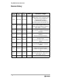
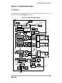
DOCUMENT NUMBER
S12TIM16B8CV1/D
TIM_16B8C
Block User Guide
Original Release Date: 28 Jul 2000
Revised: 11 Oct 2001
Motorola, Inc
Motorola reserves the right to make changes without further notice to any products herein to improve reliability, function or
design. Motorola does not assume any liability arising out of the application or use of any product or circuit described herein;
neither does it convey any license under its patent rights nor the rights of others. Motorola products are not designed, intended,
or authorized for use as components in systems intended for surgical implant into the body, or other applications intended to
support or sustain life, or for any other application in which the failure of the Motorola product could create a situation where
personal injury or death may occur. Should Buyer purchase or use Motorola products for any such unintended or unauthorized
application, Buyer shall indemnify and hold Motorola and its officers, employees, subsidiaries, affiliates, and distributors harmless
against all claims, costs, damages, and expenses, and reasonable attorney fees arising out of, directly or indirectly, any claim of
personal injury or death associated with such unintended or unauthorized use, even if such claim alleges that Motorola was
negligent regarding the design or manufacture of the part.
1
TIM_16B8C Block User Guide V01.08
Revision History
Version
Number
Revision
Dates
Effective
Date
01.00
04 Jul 2000
04 Jul 2000
01.01
28 Jul 2000
28 Jul 2000
01.02
16 Oct 2000
16 Oct 2000
01.03
23 Feb 2001
23 Feb 2001
01.04
19 Mar 2001
19 Mar 2001
01.05
27 Apr 2001
27 Apr 2001
01.06
03 Aug 2001
03 Aug 2001
01.07
11 Oct 2001
11 Oct 2001
01.08
11 Nov 2002
11 Nov 2002
2
Author
Description of Changes
This specification draft has been generated using
BARRACUDA-ECT Ref 0.5 as the reference spec.
Changed the specs as per MSRS format.
Stripped the ECT functionality
The timer now has only one 16-bit Pulse
Accumulator compared to four 8-bit PACs in ECT.
As per the MSRS2.0 format the specification draft
has been modified using MAKO-TIMER 0.1 as the
reference spec and the feedback from Munich on
MAKO-TIMER 0.1 incorporated.
Gated clock ipg_tim_core_clk and its enable signal
ipg_tim_core_clk_en is added for reducing power
consumption.
Removed Block Diagram in section ‘Signal
Description’.
Removed all internal signal description.
Removed ‘Signal Properties’ table in the ‘Signal
Description’ section.
Removed ‘Reset Summary’ table in the ‘Resets’
section.
A new and simple block diagram has been added in
place of Time Block Diagram in ‘Introduction’
section.
Headings of all register descriptions have been
changed to ‘sub sections’ from ‘figure’.
Prescale Factor column has been modified in Table
3-4.
All the pin name occurances PTx, ICx and OCx
have been replaced by IOCx . ‘Module clock’ has
been changed to ‘bus clock’
Replaced references of “n” with “x” eg.TnC to TxC
TIM_16B8C Block User Guide V01.08
Table of Contents
Section 1 Introduction
1.1
1.2
1.3
1.4
Overview. . . . . . . . . . . . . . . . . . . . . . . . . . . . . . . . . . . . . . . . . . . . . . . . . . . . . . . . . . . . . .9
Features . . . . . . . . . . . . . . . . . . . . . . . . . . . . . . . . . . . . . . . . . . . . . . . . . . . . . . . . . . . . . .9
Modes of Operation . . . . . . . . . . . . . . . . . . . . . . . . . . . . . . . . . . . . . . . . . . . . . . . . . . . . .9
Block Diagrams . . . . . . . . . . . . . . . . . . . . . . . . . . . . . . . . . . . . . . . . . . . . . . . . . . . . . . .10
Section 2 Signal Description
2.1
Overview. . . . . . . . . . . . . . . . . . . . . . . . . . . . . . . . . . . . . . . . . . . . . . . . . . . . . . . . . . . . .11
2.2
Detailed Signal Descriptions. . . . . . . . . . . . . . . . . . . . . . . . . . . . . . . . . . . . . . . . . . . . . .11
2.2.1
IOC7 – Input capture and Output compare channel 7 . . . . . . . . . . . . . . . . . . . . . . . .11
2.2.2
IOC6 – Input capture and Output compare channel 6 . . . . . . . . . . . . . . . . . . . . . . . .11
2.2.3
IOC5 – Input capture and Output compare channel 5 . . . . . . . . . . . . . . . . . . . . . . . .11
2.2.4
IOC4 – Input capture and Output compare channel 4 . . . . . . . . . . . . . . . . . . . . . . . .11
2.2.5
IOC3 – Input capture and Output compare channel 3 . . . . . . . . . . . . . . . . . . . . . . . .11
2.2.6
IOC2 – Input capture and Output compare channel 2 . . . . . . . . . . . . . . . . . . . . . . . .11
2.2.7
IOC1 – Input capture and Output compare channel 1 . . . . . . . . . . . . . . . . . . . . . . . .11
2.2.8
IOC0 – Input capture and Output compare channel 0 . . . . . . . . . . . . . . . . . . . . . . . .11
Section 3 Memory Map and Registers
3.1
Overview. . . . . . . . . . . . . . . . . . . . . . . . . . . . . . . . . . . . . . . . . . . . . . . . . . . . . . . . . . . . .13
3.2
Module Memory Map . . . . . . . . . . . . . . . . . . . . . . . . . . . . . . . . . . . . . . . . . . . . . . . . . . .13
3.3
Register Descriptions . . . . . . . . . . . . . . . . . . . . . . . . . . . . . . . . . . . . . . . . . . . . . . . . . . .14
3.3.1
Timer Input Capture/Output Compare Select (TIOS). . . . . . . . . . . . . . . . . . . . . . . . .15
3.3.2
Timer Compare Force Register (CFORC) . . . . . . . . . . . . . . . . . . . . . . . . . . . . . . . . .15
3.3.3
Output Compare 7 Mask Register (OC7M) . . . . . . . . . . . . . . . . . . . . . . . . . . . . . . . .15
3.3.4
Output Compare 7 Data Register (OC7D) . . . . . . . . . . . . . . . . . . . . . . . . . . . . . . . . .16
3.3.5
Timer Count Register (TCNT) . . . . . . . . . . . . . . . . . . . . . . . . . . . . . . . . . . . . . . . . . .16
3.3.6
Timer System Control Register 1 (TSCR1) . . . . . . . . . . . . . . . . . . . . . . . . . . . . . . . .17
3.3.7
Timer Toggle On Overflow Register 1 (TTOV). . . . . . . . . . . . . . . . . . . . . . . . . . . . . .18
3.3.8
Timer Control Register 1/Timer Control Register 2 (TCTL1/TCTL2) . . . . . . . . . . . . .18
3.3.9
Timer Control Register 3/Timer Control Register 4 (TCTL3/TCTL4) . . . . . . . . . . . . .20
3.3.10 Timer Interrupt Enable Register (TIE) . . . . . . . . . . . . . . . . . . . . . . . . . . . . . . . . . . . .20
3.3.11 Timer System Control Register 2 (TSCR2) . . . . . . . . . . . . . . . . . . . . . . . . . . . . . . . .21
3
TIM_16B8C Block User Guide V01.08
3.3.12
3.3.13
3.3.14
3.3.15
3.3.16
3.3.17
Main Timer Interrupt Flag 1 (TFLG1) . . . . . . . . . . . . . . . . . . . . . . . . . . . . . . . . . . . . .22
Main Timer Interrupt Flag 2 (TFLG2) . . . . . . . . . . . . . . . . . . . . . . . . . . . . . . . . . . . . .22
Timer Input Capture/Output Compare Registers 0-7 . . . . . . . . . . . . . . . . . . . . . . . . .23
16-Bit Pulse Accumulator Control Register (PACTL). . . . . . . . . . . . . . . . . . . . . . . . .24
Pulse Accumulator Flag Register (PAFLG) . . . . . . . . . . . . . . . . . . . . . . . . . . . . . . . .26
Pulse Accumulators Count Registers (PACNT) . . . . . . . . . . . . . . . . . . . . . . . . . . . . .26
Section 4 Functional Description
4.1
4.2
4.3
4.4
4.5
4.5.1
4.5.2
General. . . . . . . . . . . . . . . . . . . . . . . . . . . . . . . . . . . . . . . . . . . . . . . . . . . . . . . . . . . . . .29
Prescaler . . . . . . . . . . . . . . . . . . . . . . . . . . . . . . . . . . . . . . . . . . . . . . . . . . . . . . . . . . . .30
Input Capture . . . . . . . . . . . . . . . . . . . . . . . . . . . . . . . . . . . . . . . . . . . . . . . . . . . . . . . . .30
Output Compare . . . . . . . . . . . . . . . . . . . . . . . . . . . . . . . . . . . . . . . . . . . . . . . . . . . . . . .30
Pulse Accumulator . . . . . . . . . . . . . . . . . . . . . . . . . . . . . . . . . . . . . . . . . . . . . . . . . . . . .30
Event Counter Mode . . . . . . . . . . . . . . . . . . . . . . . . . . . . . . . . . . . . . . . . . . . . . . . . .31
Gated Time Accumulation Mode . . . . . . . . . . . . . . . . . . . . . . . . . . . . . . . . . . . . . . . .31
Section 5 Resets
5.1
General. . . . . . . . . . . . . . . . . . . . . . . . . . . . . . . . . . . . . . . . . . . . . . . . . . . . . . . . . . . . . .33
Section 6 Interrupts
6.1
General. . . . . . . . . . . . . . . . . . . . . . . . . . . . . . . . . . . . . . . . . . . . . . . . . . . . . . . . . . . . . .35
6.2
Description of Interrupt Operation . . . . . . . . . . . . . . . . . . . . . . . . . . . . . . . . . . . . . . . . .35
6.2.1
Channel [7:0] Interrupt (C[7:0]F) . . . . . . . . . . . . . . . . . . . . . . . . . . . . . . . . . . . . . . . .35
6.2.2
Pulse Accumulator Input Interrupt (PAOVI) . . . . . . . . . . . . . . . . . . . . . . . . . . . . . . . .35
6.2.3
Pulse Accumulator Overflow Interrupt (PAOVF) . . . . . . . . . . . . . . . . . . . . . . . . . . . .35
6.2.4
Timer Overflow Interrupt (TOF) . . . . . . . . . . . . . . . . . . . . . . . . . . . . . . . . . . . . . . . . .35
4
TIM_16B8C Block User Guide V01.08
List of Figures
Figure 1-1
Figure 4-1
Timer Block Diagram . . . . . . . . . . . . . . . . . . . . . . . . . . . . . . . . . . . . . . . . . . . . . .10
Detailed Timer Block Diagram . . . . . . . . . . . . . . . . . . . . . . . . . . . . . . . . . . . . . . .29
5
TIM_16B8C Block User Guide V01.08
6
TIM_16B8C Block User Guide V01.08
List of Tables
Table 3-1
Table 3-2
Table 3-3
Table 3-4
Table 3-5
Table 3-6
Table 6-1
Module Memory Map . . . . . . . . . . . . . . . . . . . . . . . . . . . . . . . . . . . . . . . . . . . . . .13
Compare Result Output Action . . . . . . . . . . . . . . . . . . . . . . . . . . . . . . . . . . . . . . .19
Edge Detector Circuit Configuration . . . . . . . . . . . . . . . . . . . . . . . . . . . . . . . . . . .20
Prescaler Selection . . . . . . . . . . . . . . . . . . . . . . . . . . . . . . . . . . . . . . . . . . . . . . . .21
Pin Action . . . . . . . . . . . . . . . . . . . . . . . . . . . . . . . . . . . . . . . . . . . . . . . . . . . . . . .25
Timer Clock Selection . . . . . . . . . . . . . . . . . . . . . . . . . . . . . . . . . . . . . . . . . . . . . .25
TIM_16B8C Interrupts . . . . . . . . . . . . . . . . . . . . . . . . . . . . . . . . . . . . . . . . . . . . . .35
7
TIM_16B8C Block User Guide V01.08
8
TIM_16B8C Block User Guide V01.08
Section 1 Introduction
1.1 Overview
The basic timer consists of a 16-bit, software-programmable counter driven by a seven-stage
programmable prescaler.
This timer can be used for many purposes, including input waveform measurements while simultaneously
generating an output waveform. Pulse widths can vary from microseconds to many seconds.
This timer contains 8 complete input capture/output compare channels and one pulse accumulator. The
input capture function is used to detect a selected transition edge and record the time. The output compare
function is used for generating output signals or for timer software delays. The 16-bit pulse accumulator
is used to operate as a simple event counter or a gated time accumulator. The pulse accumulator shares
timer channel 7 when in event mode.
A full access for the counter registers or the input capture/output compare registers should take place in
one clock cycle. Accessing high byte and low byte separately for all of these registers may not yield the
same result as accessing them in one word.
1.2 Features
The TIM_16B8C includes these distinctive features:
•
Eight input capture/output compare channels.
•
Clock prescaling.
•
16-bit counter.
•
16-bit pulse accumulator.
1.3 Modes of Operation
STOP:
Timer is off since clocks are stopped.
FREEZE: Timer counter keep on running, unless TSFRZ in TSCR($06) is set to one.
WAIT:
Counters keep on running, unless TSWAI in TSCR ($06) is set to one.
NORMAL:Timer counter keep on running, unless TEN in TSCR($06) is cleared.
9
TIM_16B8C Block User Guide V01.08
1.4 Block Diagrams
Figure 1-1 Timer Block Diagram
Bus clock
Prescaler
16-bit Counter
Channel 0
Input capture
Output compare
Channel 1
Input capture
Output compare
Channel 2
Input capture
Output compare
Timer overflow
interrupt
Timer channel 0
interrupt
Channel 3
Input capture
Output compare
Registers
Channel 4
Input capture
Output compare
Channel 5
Input capture
Output compare
Timer channel 7
interrupt
PA overflow
interrupt
PA input
interrupt
NOTE:
10
Channel 6
Input capture
Output compare
16-bit
Pulse accumulator
Channel 7
Input capture
Output compare
IOC0
IOC1
IOC2
IOC3
IOC4
IOC5
IOC6
IOC7
For more information see the respective functional descriptions in Section 4 of this
document.
TIM_16B8C Block User Guide V01.08
Section 2 Signal Description
2.1 Overview
The TIM_16B8C module has a total 8 external pins.
2.2 Detailed Signal Descriptions
2.2.1 IOC7 – Input capture and Output compare channel 7
This pin serves as input capture or output compare for channel 7. This can also be configured as pulse
accumulator input.
2.2.2 IOC6 – Input capture and Output compare channel 6
This pin serves as input capture or output compare for channel 6.
2.2.3 IOC5 – Input capture and Output compare channel 5
This pin serves as input capture or output compare for channel 7.
2.2.4 IOC4 – Input capture and Output compare channel 4
This pin serves as input capture or output compare for channel 4.
2.2.5 IOC3 – Input capture and Output compare channel 3
This pin serves as input capture or output compare for channel 3.
2.2.6 IOC2 – Input capture and Output compare channel 2
This pin serves as input capture or output compare for channel 2.
2.2.7 IOC1 – Input capture and Output compare channel 1
This pin serves as input capture or output compare for channel 1.
2.2.8 IOC0 – Input capture and Output compare channel 0
This pin serves as input capture or output compare for channel 0.
NOTE:
For the description of interrupts see Section 6 Interrupts.
11
TIM_16B8C Block User Guide V01.08
12
TIM_16B8C Block User Guide V01.08
Section 3 Memory Map and Registers
3.1 Overview
This section provides a detailed description of all memory and registers.
3.2 Module Memory Map
The memory map for the TIM_16B8C module is given below in Table 3-1. The Address listed for each
register is the address offset. The total address for each register is the sum of the base address for the
TIM_16B8C module and the address offset for each register.
Table 3-1 Module Memory Map
Offset
Use
Access
$_00
Timer Input Capture/Output Compare Select (TIOS)
Read/Write
$_01
Timer Compare Force Register (CFORC)
Read/Write1
$_02
Output Compare 7 Mask Register (OC7M)
Read/Write
$_03
Output Compare 7 Data Register (OC7D)
Read/Write
$_04
Timer Count Register (TCNT(hi))
Read/Write2
$_05
Timer Count Register (TCNT(lo))
Read/Write2
$_06
Timer System Control Register1 (TSCR1)
Read/Write
$_07
Timer Toggle Overflow Register (TTOV)
Read/Write
$_08
Timer Control Register1 (TCTL1)
Read/Write
$_09
Timer Control Register2 (TCTL2)
Read/Write
$_0A
Timer Control Register3 (TCTL3)
Read/Write
$_0B
Timer Control Register4 (TCTL4)
Read/Write
$_0C
Timer Interrupt Enable Register (TIE)
Read/Write
$_0D
Timer System Control Register2 (TSCR2)
Read/Write
$_0E
Main Timer Interrupt Flag1 (TFLG1)
Read/Write
$_0F
Main Timer Interrupt Flag2 (TFLG2)
Read/Write
$_10
Timer Input Capture/Output Compare Register0
(TC0(hi))
Read/Write3
$_11
Timer Input Capture/Output Compare Register0
(TC0(lo))
Read/Write3
$_12
Timer Input Capture/Output Compare Register1
(TC1(hi))
Read/Write3
$_13
Timer Input Capture/Output Compare Register1
(TC1(lo))
Read/Write3
$_14
Timer Input Capture/Output Compare Register2
(TC2(hi))
Read/Write3
$_15
Timer Input Capture/Output Compare Register2
(TC2(lo))
Read/Write3
$_16
Timer Input Capture/Output Compare Register3
(TC3(hi))
Read/Write3
13
TIM_16B8C Block User Guide V01.08
Table 3-1 Module Memory Map
$_17
Timer Input Capture/Output Compare Register3
(TC3(lo))
Read/Write3
$_18
Timer Input Capture/Output Compare Register4
(TC4(hi))
Read/Write3
$_19
Timer Input Capture/Output Compare Register4
(TC4(lo))
Read/Write3
$_1A
Timer Input Capture/Output Compare Register5
(TC5(hi))
Read/Write3
$_1B
Timer Input Capture/Output Compare Register5
(TC5(lo))
Read/Write3
$_1C
Timer Input Capture/Output Compare Register6
(TC6(hi))
Read/Write3
$_1D
Timer Input Capture/Output Compare Register6
(TC6(lo))
Read/Write3
$_1E
Timer Input Capture/Output Compare Register7
(TC7(hi))
Read/Write3
$_1F
Timer Input Capture/Output Compare Register7
(TC7(lo))
Read/Write3
$_20
16-Bit Pulse Accumulator Control Register (PACTL)
Read/Write
$_21
Pulse Accumulator Flag Register (PAFLG)
Read/Write
$_22
Pulse Accumulator Count Register
(PACNT(hi))
Read/Write
$_23
Pulse Accumulator Count Register
(PACNT(lo))
Read/Write
$_24 – $_2C
Reserved
Write has no effect
Return 0 on read
$_2D
Timer Test Register (TIMTST)
Read/Write2
$-2E – $_2F
Reserved
Write has no effect
Return 0 on read
NOTE: 1. Always read $00.
2. Only writable in special modes (test_mode = 1).
3. Write to these registers have no meaning or effect during input capture.
3.3 Register Descriptions
This section consists of register descriptions in address order. Each description includes a standard register
diagram with an associated figure number. Details of register bit and field function follow the register
diagrams, in bit order.
14
TIM_16B8C Block User Guide V01.08
3.3.1 Timer Input Capture/Output Compare Select (TIOS)
Register offset: $_00
R
W
RESET:
Bit 7
6
5
4
3
2
1
Bit 0
IOS7
IOS6
IOS5
IOS4
IOS3
IOS2
IOS1
IOS0
0
0
0
0
0
0
0
0
2
1
Bit 0
Read or write anytime.
IOS[7:0] — Input Capture or Output Compare Channel Configuration
1 = The corresponding channel acts as an output compare.
0 = The corresponding channel acts as an input capture.
3.3.2 Timer Compare Force Register (CFORC)
Register offset:$_01
Bit 7
6
5
4
3
R
0
0
0
0
0
0
0
0
W
FOC7
FOC6
FOC5
FOC4
FOC3
FOC2
FOC1
FOC0
RESET:
0
0
0
0
0
0
0
0
Read anytime but will always return $00 (1 state is transient). Write anytime.
FOC[7:0] — Force Output Compare Action for Channel 7-0
A write to this register with the corresponding data bit(s) set causes the action which is programmed
for output compare “x” to occur immediately. The action taken is the same as if a successful
comparison had just taken place with the TCx register except the interrupt flag does not get set.
NOTE:
A successful channel 7 output compare overrides any channel 6:0 compares. If
forced output compare on any channel occurs at the same time as the successful
output compare then forced output compare action will take precedence and
interrupt flag won’t get set.
3.3.3 Output Compare 7 Mask Register (OC7M)
Register offset:$_02
R
W
RESET:
Bit 7
6
5
4
3
2
1
Bit 0
OC7M7
OC7M6
OC7M5
OC7M4
OC7M3
OC7M2
OC7M1
OC7M0
0
0
0
0
0
0
0
0
Read or write anytime.
Setting the OC7Mx (x ranges from 0 to 6) will set the corresponding port to be an output port when the
corresponding TIOSx (x ranges from 0 to 6) bit is set to be an output compare.
15
TIM_16B8C Block User Guide V01.08
NOTE:
A successful channel 7 output compare overrides any channel 6:0 compares. For
each OC7M bit that is set, the output compare action reflects the corresponding
OC7D bit.
3.3.4 Output Compare 7 Data Register (OC7D)
Register offset:$_03
R
W
Bit 7
6
5
4
3
2
1
Bit 0
OC7D7
OC7D6
OC7D5
OC7D4
OC7D3
OC7D2
OC7D1
OC7D0
0
0
0
0
0
0
0
0
RESET:
Read or write anytime.
A channel 7 output compare can cause bits in the output compare 7 data register to transfer to the timer
port data register depending on the output compare 7 mask register.
3.3.5 Timer Count Register (TCNT)
Register offset:$_04-$_05
Bit 15
14
13
12
11
10
9
8
7
6
5
4
3
2
1
Bit 0
W
tcnt
15
tcnt
14
tcnt
13
tcnt
12
tcnt
11
tcnt
10
tcnt
9
tcnt
8
tcnt
7
tcnt
6
tcnt
5
tcnt
4
tcnt
3
tcnt
2
tcnt
1
tcnt t
0
RESET:
0
0
0
0
0
0
0
0
0
0
0
0
0
0
0
0
R
The 16-bit main timer is an up counter.
A full access for the counter register should take place in one clock cycle. A separate read/write for high
byte and low byte will give a different result than accessing them as a word.
Read anytime.
Write has no meaning or effect in the normal mode; only writable in special modes (test_mode = 1).
The period of the first count after a write to the TCNT registers may be a different size because the write
is not synchronized with the prescaler clock.
16
TIM_16B8C Block User Guide V01.08
3.3.6 Timer System Control Register 1 (TSCR1)
Register offset:$_06
R
W
RESET:
Bit 7
6
5
4
TEN
TSWAI
TSFRZ
TFFCA
0
0
0
0
3
2
1
Bit 0
0
0
0
0
0
0
0
0
= Unimplemented or Reserved
Read or write anytime.
TEN — Timer Enable
1 = Allows the timer to function normally.
0 = Disables the main timer, including the counter. Can be used for reducing power consumption.
If for any reason the timer is not active, there is no ÷64 clock for the pulse accumulator since the ÷64
is generated by the timer prescaler.
TSWAI — Timer Module Stops While in Wait
1 = Disables the timer module when the MCU is in the wait mode. Timer interrupts cannot be used
to get the MCU out of wait.
0 = Allows the timer module to continue running during wait.
TSWAI also affects pulse accumulator.
TSFRZ — Timer Stops While in Freeze Mode
1 = Disables the timer counter whenever the MCU is in freeze mode. This is useful for emulation.
0 = Allows the timer counter to continue running while in freeze mode.
TSFRZ does not stop the pulse accumulator.
TFFCA — Timer Fast Flag Clear All
1 = For TFLG1($0E), a read from an input capture or a write to the output compare channel
($10–$1F) causes the corresponding channel flag, CnF, to be cleared. For TFLG2 ($0F), any
access to the TCNT register ($04, $05) clears the TOF flag. Any access to the PACNT registers
($22, $23) clears the PAOVF and PAIF flags in the PAFLG register ($21). This has the
advantage of eliminating software overhead in a separate clear sequence. Extra care is required
to avoid accidental flag clearing due to unintended accesses.
0 = Allows the timer flag clearing to function normally.
17
TIM_16B8C Block User Guide V01.08
3.3.7 Timer Toggle On Overflow Register 1 (TTOV)
Register offset:$_07
Bit 7
6
5
4
3
2
1
Bit 0
TOV7
TOV6
TOV5
TOV4
TOV3
TOV2
TOV1
TOV0
0
0
0
0
0
0
0
0
R
W
RESET
Read or write anytime.
TOVx — Toggle On Overflow Bits
TOVx toggles output compare pin on overflow. This feature only takes effect when in output compare
mode. When set, it takes precedence over forced output compare but not channel 7 override events.
1 = Toggle output compare pin on overflow feature enabled.
0 = Toggle output compare pin on overflow feature disabled.
3.3.8 Timer Control Register 1/Timer Control Register 2 (TCTL1/TCTL2)
Register offset:$_08
R
W
RESET
7
6
5
4
3
2
1
Bit 0
OM7
OL7
OM6
OL6
OM5
OL5
OM4
OL4
0
0
0
0
0
0
0
0
Bit 7
6
5
4
3
2
1
Bit 0
OM3
OL3
OM2
OL2
OM1
OL1
OM0
OL0
0
0
0
0
0
0
0
0
Register offset:$_09
R
W
RESET
Read or write anytime.
OMx — Output Mode
OLx — Output Level
These eight pairs of control bits are encoded to specify the output action to be taken as a result of a
successful OCx compare. When either OMx or OLx is one, the pin associated with OCx becomes an
output tied to OCx.
18
TIM_16B8C Block User Guide V01.08
NOTE:
To enable output action by OMx and OLx bits on timer port, the corresponding bit
in OC7M should be cleared.
Table 3-2 Compare Result Output Action
OMx
OLx
Action
0
0
Timer disconnected from output pin logic
0
1
Toggle OCx output line
1
0
Clear OCx output line to zero
1
1
Set OCx output line to one
To operate the 16-bit pulse accumulator independently of input capture or output compare 7 and 0
respectively the user must set the corresponding bits IOSx = 1, OMx = 0 and OLx = 0. OC7M7 in the
OC7M register must also be cleared.
19
TIM_16B8C Block User Guide V01.08
3.3.9 Timer Control Register 3/Timer Control Register 4 (TCTL3/TCTL4)
Register offset:$_0A
R
W
RESET:
Bit 7
6
5
4
3
2
1
Bit 0
EDG7B
EDG7A
EDG6B
EDG6A
EDG5B
EDG5A
EDG4B
EDG4A
0
0
0
0
0
0
0
0
Bit 7
6
5
4
3
2
1
Bit 0
EDG3B
EDG3A
EDG2B
EDG2A
EDG1B
EDG1A
EDG0B
EDG0A
0
0
0
0
0
0
0
0
Register offset:$_0B
R
W
RESET:
Read or write anytime.
EDGnB, EDGnA — Input Capture Edge Control
These eight pairs of control bits configure the input capture edge detector circuits.
Table 3-3 Edge Detector Circuit Configuration
EDGnB
EDGnA
Configuration
0
0
Capture disabled
0
1
Capture on rising edges only
1
0
Capture on falling edges only
1
1
Capture on any edge (rising or falling)
3.3.10 Timer Interrupt Enable Register (TIE)
Register offset:$_0C
R
W
RESET:
Bit 7
6
5
4
3
2
1
Bit 0
C7I
C6I
C5I
C4I
C3I
C2I
C1I
C0I
0
0
0
0
0
0
0
0
Read or write anytime.
The bits in TIE correspond bit-for-bit with the bits in the TFLG1 status register. If cleared, the
corresponding flag is disabled from causing a hardware interrupt. If set, the corresponding flag is enabled
to cause a interrupt.
C7I–C0I — Input Capture/Output Compare “x” Interrupt Enable.
20
TIM_16B8C Block User Guide V01.08
3.3.11 Timer System Control Register 2 (TSCR2)
Register offset:$_0D
Bit 7
R
W
RESET:
TOI
0
6
5
4
0
0
0
0
0
0
3
2
1
Bit 0
TCRE
PR2
PR1
PR0
0
0
0
0
= Unimplemented or Reserved
Read or write anytime.
TOI — Timer Overflow Interrupt Enable
1 = Hardware interrupt requested when TOF flag set.
0 = Interrupt inhibited.
TCRE — Timer Counter Reset Enable
This bit allows the timer counter to be reset by a successful output compare 7 event. This mode of
operation is similar to an up-counting modulus counter.
1 = Counter reset by a successful output compare 7.
0 = Counter reset inhibited and counter free runs.
If TC7 = $0000 and TCRE = 1, TCNT will stay at $0000 continuously. If TC7 = $FFFF and TCRE =
1, TOF will never be set when TCNT is reset from $FFFF to $0000.
PR2, PR1, PR0 — Timer Prescaler Select
These three bits select the frequency of the timer prescaler clock derived from the Bus Clock as shown
in Table 3-4.
Table 3-4 Timer Clock Selection
PR2
PR1
PR0
Timer Clock
0
0
0
Bus Clock / 1
0
0
1
Bus Clock / 2
0
1
0
Bus Clock / 4
0
1
1
Bus Clock / 8
1
0
0
Bus Clock / 16
1
0
1
Bus Clock / 32
1
1
0
Bus Clock / 64
1
1
1
Bus Clock / 128
The newly selected prescale factor will not take effect until the next synchronized edge where all
prescale counter stages equal zero.
21
TIM_16B8C Block User Guide V01.08
3.3.12 Main Timer Interrupt Flag 1 (TFLG1)
Register offset:$_0E
R
W
RESET:
Bit 7
6
5
4
3
2
1
Bit 0
C7F
C6F
C5F
C4F
C3F
C2F
C1F
C0F
0
0
0
0
0
0
0
0
These flags are set when an input capture or output compare event occurs. Clear a channel flag by writing
one to it.
Read anytime. Write used in the clearing mechanism (set bits cause corresponding bits to be cleared).
Writing a zero will not affect current status of the bit.
When TFFCA bit in TSCR register is set, a read from an input capture or a write into an output compare
channel ($10–$1F) will cause the corresponding channel flag CxF to be cleared.
C7F–C0F — Input Capture/Output Compare Channel “x” Flag.
3.3.13 Main Timer Interrupt Flag 2 (TFLG2)
Register offset:$_0F
Bit 7
R
W
RESET:
TOF
0
6
5
4
3
2
1
Bit 0
0
0
0
0
0
0
0
0
0
0
0
0
0
0
= Unimplemented or Reserved
TFLG2 indicates when interrupt conditions have occurred. To clear a bit in the flag register, write the bit
to one.
Read anytime. Write used in clearing mechanism (set bits cause corresponding bits to be cleared).
Any access to TCNT will clear TFLG2 register if the TFFCA bit in TSCR register is set.
TOF — Timer Overflow Flag
Set when 16-bit free-running timer overflows from $FFFF to $0000. This bit is cleared automatically
by a write to the TFLG2 register with bit 7 set. (See also TCRE control bit explanation.)
22
TIM_16B8C Block User Guide V01.08
3.3.14 Timer Input Capture/Output Compare Registers 0-7
TC0 — Timer Input Capture/Output Compare Register 0 Register offset:$_10–$_11
Bit 15
14
13
12
11
10
9
8
7
6
5
4
3
2
1
BIt 0
R
W
tc0
15
tc0
14
tc0
13
tc0
12
tc0
11
tc0
10
tc0
9
tc0
8
tc0
7
tc0
6
tc0
5
tc0
4
tc0
3
tc0
2
tc0
1
tc0
0
RESET
0
0
0
0
0
0
0
0
0
0
0
0
0
0
0
0
TC1 — Timer Input Capture/Output Compare Register 1 Register offset:$_12–$_13
Bit 15
14
13
12
11
10
9
8
7
6
5
4
3
2
1
Bit 0
R
W
tc1
15
tc1
14
tc1
13
tc1
12
tc1
11
tc1
10
tc1
9
tc1
8
tc1
7
tc1
6
tc1
5
tc1
4
tc1
3
tc1
2
tc1
1
tc1
0
RESET
0
0
0
0
0
0
0
0
0
0
0
0
0
0
0
0
TC2 — Timer Input Capture/Output Compare Register 2 Register offset:$_14–$_15
Bit 15
14
13
12
11
10
9
8
7
6
5
4
3
2
1
Bit 0
R
W
tc2
15
tc2
14
tc2
13
tc2
12
tc2
11
tc2
10
tc2
9
tc2
8
tc2
7
tc2
6
tc2
5
tc2
4
tc2
3
tc2
2
tc2
1
tc2
0
RESET
0
0
0
0
0
0
0
0
0
0
0
0
0
0
0
0
TC3 — Timer Input Capture/Output Compare Register 3 Register offset:$_16–$_17
Bit 15
14
13
12
11
10
9
8
7
6
5
4
3
2
1
Bit 0
R
W
tc3
15
tc3
14
tc13
13
tc3
12
tc3
11
tc3
10
tc3
9
tc3
8
tc3
7
tc3
6
tc3
5
tc3
4
tc3
3
tc3
2
tc3
1
tc3
0
RESET
0
0
0
0
0
0
0
0
0
0
0
0
0
0
0
0
TC4 — Timer Input Capture/Output Compare Register 4 Register offset:$_18–$_19
Bit 15
14
13
12
11
10
9
8
7
6
5
4
3
2
1
Bit 0
R
W
tc4
15
tc4
14
tc4
13
tc4
12
tc4
11
tc4
10
tc4
9
tc4
8
tc4
7
tc4
6
tc4
5
tc4
4
tc4
3
tc4
2
tc4
1
tc4
0
RESET
0
0
0
0
0
0
0
0
0
0
0
0
0
0
0
0
TC5 — Timer Input Capture/Output Compare Register 5 Register offset:$_1A–$_1B
Bit 15
14
13
2
11
10
9
8
7
6
5
4
3
2
1
Bit 0
R
W
tc5
15
tc5
14
tc5
13
tc5
12
tc5
11
tc5
10
tc5
9
tc5
8
tc5
7
tc5
6
tc5
5
tc5
4
tc5
3
tc5
2
tc5
1
tc5
0
RESET
0
0
0
0
0
0
0
0
0
0
0
0
0
0
0
0
TC6 — Timer Input Capture/Output Compare Register 6 Register offset:$_1C–$_1D
Bit 15
14
13
12
11
10
9
8
7
6
5
4
3
2
1
Bit 0
R
W
tc6
15
tc6
14
tc6
13
tc6
12
tc6
11
tc6
10
tc6
9
tc6
8
tc6
7
tc6
6
tc6
5
tc6
4
tc6
3
tc6
2
tc6
1
tc6
0
RESET
0
0
0
0
0
0
0
0
0
0
0
0
0
0
0
0
23
TIM_16B8C Block User Guide V01.08
TC7 — Timer Input Capture/Output Compare Register 7 Register offset:$_1E–$_1F
Bit 15
14
13
2
11
0
9
8
7
6
5
4
3
2
1
Bit 0
R
W
tc7
15
tc7
14
tc7
13
tc7
12
tc7
11
tc7
10
tc7
9
tc7
8
tc7
7
tc7
6
tc7
5
tc7
4
tc7
3
tc7
2
tc7
1
tc7
0
RESET
0
0
0
0
0
0
0
0
0
0
0
0
0
0
0
0
Depending on the TIOS bit for the corresponding channel, these registers are used to latch the value of the
free-running counter when a defined transition is sensed by the corresponding input capture edge detector
or to trigger an output action for output compare.
Read anytime.Write anytime for output compare function.Writes to these registers have no meaning or
effect during input capture. All timer input capture/output compare registers are reset to $0000.
NOTE:
Read/Write access in byte mode for high byte should takes place before low byte
otherwise it will give a different result.
3.3.15 16-Bit Pulse Accumulator Control Register (PACTL)
Register offset:$_20
BIT 7
R
0
W
RESET:
0
6
5
4
3
2
1
BIT 0
PAEN
PAMOD
PEDGE
CLK1
CLK0
PAOVI
PAI
0
0
0
0
0
0
0
= Unimplemented or Reserved
When PAEN is set, the PACT is enabled.The PACT shares the input pin with IOC7.
Read: any time
Write: any time
PAEN — Pulse Accumulator System Enable
1 = Pulse Accumulator system enabled.
0 = 16-Bit Pulse Accumulator system disabled.
PAEN is independent from TEN. With timer disabled, the pulse accumulator can still function unless
pulse accumulator is disabled.
PAMOD — Pulse Accumulator Mode
This bit is active only when the Pulse Accumulator is enabled (PAEN = 1).
1 = gated time accumulation mode.
0 = event counter mode.
PEDGE — Pulse Accumulator Edge Control
This bit is active only when the Pulse Accumulator is enabled (PAEN = 1).
24
TIM_16B8C Block User Guide V01.08
For PAMOD bit = 0 (event counter mode).
1 = rising edges on IOC7 pin cause the count to be incremented.
0 = falling edges on IOC7 pin cause the count to be incremented.
For PAMOD bit = 1 (gated time accumulation mode).
1 = IOC7 input pin low enables M (bus clock) divided by 64 clock to Pulse Accumulator and the
trailing rising edge on IOC7 sets the PAIF flag.
0 = IOC7 input pin high enables M (bus clock) divided by 64 clock to Pulse Accumulator and the
trailing falling edge on IOC7 sets the PAIF flag.
Table 3-5 Pin Action
PAMOD
PEDGE
Pin Action
0
0
Falling edge
0
1
Rising edge
1
0
Div. by 64 clock enabled with pin high level
1
1
Div. by 64 clock enabled with pin low level
If the timer is not active (TEN = 0 in TSCR), there is no divide-by-64 since the ÷64 clock is generated by
the timer prescaler.
CLK1, CLK0 — Clock Select Bits
Table 3-6 Timer Clock Selection
CLK1
CLK0
Timer Clock
0
0
Use timer prescaler clock as timer counter clock
0
1
Use PACLK as input to timer counter clock
1
0
Use PACLK/256 as timer counter clock frequency
1
1
Use PACLK/65536 as timer counter clock frequency
For the description of PACLK please refer Figure 1-2 16-Bit Pulse Accumulator Block Diagram.
If the pulse accumulator is disabled (PAEN = 0), the prescaler clock from the timer is always used as an
input clock to the timer counter. The change from one selected clock to the other happens immediately
after these bits are written.
PAOVI — Pulse Accumulator Overflow Interrupt enable
1 = interrupt requested if PAOVF is set.
0 = interrupt inhibited.
PAI — Pulse Accumulator Input Interrupt enable
1 = interrupt requested if PAIF is set.
0 = interrupt inhibited.
25
TIM_16B8C Block User Guide V01.08
3.3.16 Pulse Accumulator Flag Register (PAFLG)
Register offset:$_21
BIT 7
6
5
4
3
2
0
0
0
0
0
0
0
0
0
0
0
0
R
W
RESET:
1
BIT 0
PAOVF
PAIF
0
0
= Unimplemented or Reserved
Read or write anytime. When the TFFCA bit in the TSCR register is set, any access to the PACNT register
will clear all the flags in the PAFLG register.
PAOVF — Pulse Accumulator Overflow Flag
Set when the 16-bit pulse accumulator overflows from $FFFF to $0000.
This bit is cleared automatically by a write to the PAFLG register with bit 1 set.
PAIF — Pulse Accumulator Input edge Flag
Set when the selected edge is detected at the IOC7 input pin.In event mode the event edge triggers
PAIF and in gated time accumulation mode the trailing edge of the gate signal at the IOC7 input pin
triggers PAIF.
This bit is cleared by a write to the PAFLG register with bit 0 set.
Any access to the PACNT register will clear all the flags in this register when TFFCA bit in register
TSCR($06) is set.
3.3.17 Pulse Accumulators Count Registers (PACNT)
Register offset:$_22-$_23
Bit 15
R
W
14
13
12
11
10
9
8
7
6
5
4
3
2
1
Bit 0
pacnt pacnt pacnt pacnt pacnt pacnt pacnt pacnt pacnt pacnt pacnt pacnt pacnt pacnt pacnt pacnt
15
14
13
12
11
10
9
8
7
6
5
4
3
2
1
0
RESET:
0
0
0
0
0
0
0
0
0
0
0
0
0
0
0
0
Read or write any time.
These registers contain the number of active input edges on its input pin since the last reset.
When PACNT overflows from $FFFF to $0000, the Interrupt flag PAOVF in PAFLG ($21) is set.
Full count register access should take place in one clock cycle. A separate read/write for high byte and low
byte will give a different result than accessing them as a word.
NOTE:
26
Reading the pulse accumulator counter registers immediately after an active edge
on the pulse accumulator input pin may miss the last count since the input has to be
synchronized with the bus clock first.
TIM_16B8C Block User Guide V01.08
27
TIM_16B8C Block User Guide V01.08
28
TIM_16B8C Block User Guide V01.08
Section 4 Functional Description
4.1 General
This section provides a complete functional description of the timer TIM_16B8C block. Please refer to the
detailed timer block diagram in Figure 4-1 as necessary.
Figure 4-1 Detailed Timer Block Diagram
Bus Clock
CLK[1:0]
PR[2:1:0]
channel 7 output
compare
PACLK
PACLK/256
PACLK/65536
MUX
TCRE
PRESCALER
CxI
TCNT(hi):TCNT(lo)
CxF
CLEAR COUNTER
16-BIT COUNTER
TOF
INTERRUPT
LOGIC
TOI
TE
TOF
CHANNEL 0
16-BIT COMPARATOR
OM:OL0
TC0
EDG0A
C0F
C0F
EDGE
DETECT
EDG0B
CH. 0 CAPTURE
IOC0 PIN
LOGIC CH. 0COMPARE
TOV0
IOC0 PIN
IOC0
CHANNEL 1
16-BIT COMPARATOR
OM:OL1
TC1
EDGE
DETECT
EDG1B
EDG1A
C1F
C1F
CH. 1 CAPTURE
IOC1 PIN
LOGIC CH. 1 COMPARE
TOV1
IOC1 PIN
IOC1
CHANNEL2
CHANNEL7
16-BIT COMPARATOR
OM:O73
EDG7A
EDGE
DETECT
EDG7B
PAOVF
C7F
C7F
TC7
PACNT(hi):PACNT(lo)
TOV7
IOC7
PEDGE
PAE
PACLK/65536
CH.7 CAPTURE
IOC7 PIN PA INPUT
LOGIC CH. 7 COMPARE IOC7 PIN
EDGE
DETECT
16-BIT COUNTER
PACLK
PACLK/256
PAMOD
INTERRUPT
REQUEST
INTERRUPT
LOGIC
PAIF
DIVIDE-BY-64
PAOVI
PAI
PAOVF
PAIF
Bus Clock
PAOVF
PAOVI
29
TIM_16B8C Block User Guide V01.08
4.2 Prescaler
The prescaler divides the bus clock by 1,2,4,8,16,32,64 or 128. The prescaler select bits, PR[2:0], select
the prescaler divisor. PR[2:0] are in timer system control register 2 (TSCR2).
4.3 Input Capture
Clearing the I/O (input/output) select bit, IOSx, configures channel x as an input capture channel. The
input capture function captures the time at which an external event occurs. When an active edge occurs on
the pin of an input capture channel, the timer transfers the value in the timer counter into the timer channel
registers, TCx.
The minimum pulse width for the input capture input is greater than two bus clocks.
An input capture on channel x sets the CxF flag. The CxI bit enables the CxF flag to generate interrupt
requests.
4.4 Output Compare
Setting the I/O select bit, IOSx, configures channel x as an output compare channel. The output compare
function can generate a periodic pulse with a programmable polarity, duration, and frequency. When the
timer counter reaches the value in the channel registers of an output compare channel, the timer can set,
clear, or toggle the channel pin. An output compare on channel x sets the CxF flag. The CxI bit enables
the CxF flag to generate interrupt requests.
The output mode and level bits, OMx and OLx, select set, clear, toggle on output compare. Clearing both
OMx and OLx disconnects the pin from the output logic.
Setting a force output compare bit, FOCx, causes an output compare on channel x. A forced output
compare does not set the channel flag.
A successful output compare on channel 7 overrides output compares on all other output compare
channels. The output compare 7 mask register masks the bits in the output compare 7 data register. The
timer counter reset enable bit, TCRE, enables channel 7 output compares to reset the timer counter. A
channel 7 output compare can reset the timer counter even if the IOC7 pin is being used as the pulse
accumulator input.
Writing to the timer port bit of an output compare pin does not affect the pin state. The value written is
stored in an internal latch. When the pin becomes available for general-purpose output, the last value
written to the bit appears at the pin.
4.5 Pulse Accumulator
The pulse accumulator (PACNT) is a 16-bit counter that can operate in two modes:
Event counter mode --- Counting edges of selected polarity on the pulse accumulator input pin, PAI.
30
TIM_16B8C Block User Guide V01.08
Gated time accumulation mode --- Counting pulses from a divide-by-64 clock. The PAMOD bit selects
the mode of operation.
The minimum pulse width for the PAI input is greater than two bus clocks.
4.5.1 Event Counter Mode
Clearing the PAMOD bit configures the PACNT for event counter operation. An active edge on the IOC7
pin increments the pulse accumulator counter. The PEDGE bit selects falling edges or rising edges to
increment the count.
NOTE:
The PACNT input and timer channel 7 use the same pin IOC7. To use the IOC7,
disconnect it from the output logic by clearing the channel 7 output mode and
output level bits, OM7 and OL7. Also clear the channel 7 output compare 7 mask
bit, OC7M7.
The Pulse Accumulator counter register reflect the number of active input edges on the PACNT input pin
since the last reset.
The PAOVF bit is set when the accumulator rolls over from $FFFF to $0000. The pulse accumulator
overflow interrupt enable bit, PAOVI, enables the PAOVF flag to generate interrupt requests.
NOTE:
The pulse accumulator counter can operate in event counter mode even when the
timer enable bit, TEN, is clear.
4.5.2 Gated Time Accumulation Mode
Setting the PAMOD bit configures the pulse accumulator for gated time accumulation operation. An active
level on the PACNT input pin enables a divided-by-64 clock to drive the pulse accumulator. The PEDGE
bit selects low levels or high levels to enable the divided-by-64 clock.
The trailing edge of the active level at the IOC7 pin sets the PAIF. The PAI bit enables the PAIF flag to
generate interrupt requests.
The pulse accumulator counter register reflect the number of pulses from the divided-by-64 clock since
the last reset.
NOTE:
The timer prescaler generates the divided-by-64 clock. If the timer is not active,
there is no divided-by-64 clock.
31
TIM_16B8C Block User Guide V01.08
32
TIM_16B8C Block User Guide V01.08
Section 5 Resets
5.1 General
The reset state of each individual bit is listed within the Register Description section (see Section 3
Memory Map and Registers) which details the registers and their bit-fields.
33
TIM_16B8C Block User Guide V01.08
34
TIM_16B8C Block User Guide V01.08
Section 6 Interrupts
6.1 General
This section describes interrupts originated by the TIM_16B8C block. Table 6-1 lists the interrupts
generated by the TIM_16B8C to communicate with the MCU.
Table 6-1 TIM_16B8C Interrupts
1
Interrupt
Offset
Vector1
C[7:0]F
-
-
Priority1
Source
Description
-
Timer Channel 7-0
Active high timer channel interrupts 7-0
Active high pulse accumulator input interrupt
PAOVI
-
-
-
Pulse Accumulator
Input
PAOVF
-
-
-
Pulse Accumulator
Overflow
Pulse accumulator overflow interrupt
TOF
-
-
-
Timer Overflow
Timer Overflow interrupt
NOTES:
1. Chip Dependent.
6.2 Description of Interrupt Operation
The TIM_16B8C uses a total of 11 interrupt vectors. The interrupt vector offsets and interrupt numbers
are chip dependent.
6.2.1 Channel [7:0] Interrupt (C[7:0]F)
This active high outputs will be asserted by the module to request a timer channel 7 – 0 interrupt to be
serviced by the system controller.
6.2.2 Pulse Accumulator Input Interrupt (PAOVI)
This active high output will be asserted by the module to request a timer pulse accumulator input interrupt
to be serviced by the system controller.
6.2.3 Pulse Accumulator Overflow Interrupt (PAOVF)
This active high output will be asserted by the module to request a timer pulse accumulator overflow
interrupt to be serviced by the system controller.
6.2.4 Timer Overflow Interrupt (TOF)
This active high output will be asserted by the module to request a timer overflow interrupt to be serviced
by the system controller.
35
TIM_16B8C Block User Guide V01.08
36
TIM_16B8C Block User Guide V01.08
User Guide End Sheet
37
TIM_16B8C Block User Guide V01.08
FINAL PAGE OF
38
PAGES
38