1
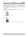
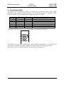
SIS Documentation
SIS3803
Scaler/Counter
SIS3803
VME Scaler/Counter
User Manual
SIS GmbH
Moorhof 2d
22399 Hamburg
Germany
Phone: ++49 (0) 40 60 87 305 0
Fax:
++49 (0) 40 60 87 305 20
email: [email protected]
http://www.struck.de
Version: 1.2 as of 20.12.99
Page 1 of 38
SIS Documentation
SIS3803
Scaler/Counter
Revision Table:
Revision
1.0
1.1
1.2
Page 2 of 38
Date
28.07.98
18.09.98
20.12.99
Modification
Generation
FIFO flag changes V2/V3 PAL
Introduction of revision table
Inline front panel design
SIS Documentation
SIS3803
Scaler/Counter
1 Table of contents
1
2
3
Table of contents...............................................................................................................................................................3
Introduction........................................................................................................................................................................5
Technical Properties/Features.........................................................................................................................................6
3.1
Board Layout.............................................................................................................................................................6
3.2
Counter Design and Modus Operandi...................................................................................................................7
3.3
Count Enable Logic..................................................................................................................................................8
3.4
Clear Logic.................................................................................................................................................................8
4
Getting Started...................................................................................................................................................................9
4.1
Factory Default Settings..........................................................................................................................................9
4.1.1
Adressing..........................................................................................................................................................9
4.1.2
System Reset Behaviour...............................................................................................................................10
5
Firmware Selection .........................................................................................................................................................10
5.1
Examples ..................................................................................................................................................................10
6
Front Panel LEDs ............................................................................................................................................................11
7
VME addressing..............................................................................................................................................................12
7.1
Address Space.........................................................................................................................................................12
7.2
Base Address...........................................................................................................................................................12
7.2.1
VME.................................................................................................................................................................12
7.2.2
VIPA/VME64x...............................................................................................................................................12
7.3
Address Map ...........................................................................................................................................................13
8
Register Description .......................................................................................................................................................14
8.1
Status Register (0x0)..............................................................................................................................................14
8.2
Control Register (0x0)...........................................................................................................................................15
8.3
Module Identification and IRQ control register (0x4)......................................................................................16
8.4
Count disable register 0xC ....................................................................................................................................17
8.5
Overflow registers 0x380, 0x3A0........................................................................................................................17
8.6
Broadcast Addressing............................................................................................................................................17
9
VME Interrupts ...............................................................................................................................................................19
10
Data Format..................................................................................................................................................................20
10.1 D16............................................................................................................................................................................20
10.2 D32............................................................................................................................................................................20
11
Readout Schemes ........................................................................................................................................................20
11.1 Read Shadow Register...........................................................................................................................................20
11.2 Read and Clear all Counters .................................................................................................................................20
11.3 Read Counter...........................................................................................................................................................20
12
Input Configuration ....................................................................................................................................................21
12.1 ECL...........................................................................................................................................................................21
12.2 NIM ...........................................................................................................................................................................22
12.3 TTL............................................................................................................................................................................23
12.3.1
TTL/LEMO.....................................................................................................................................................23
12.3.2
TTL/Flat Cable ...............................................................................................................................................23
13
Connector Specification.............................................................................................................................................23
14
Control Input Modes ..................................................................................................................................................24
15
Signal Specification....................................................................................................................................................25
15.1 Control Signals ........................................................................................................................................................25
15.2 Inputs ........................................................................................................................................................................25
16
Operating Conditions.................................................................................................................................................25
16.1 Power Consumption/Voltage requirement.........................................................................................................25
16.2 Cooling.....................................................................................................................................................................25
16.3 Insertion/Removal...................................................................................................................................................25
17
Test................................................................................................................................................................................26
17.1 LED (selftest)..........................................................................................................................................................26
17.2 Internal pulser tests ................................................................................................................................................26
17.2.1
Single Pulse....................................................................................................................................................26
17.2.2
25 MHz Pulser................................................................................................................................................26
17.3 Reference pulser channel 1 ...................................................................................................................................26
17.4 Signal-Input Priority...............................................................................................................................................26
Page 3 of 38
SIS Documentation
18
SIS3803
Scaler/Counter
Software Support ........................................................................................................................................................27
Contents of the included Floppy..........................................................................................................................27
19
Appendix......................................................................................................................................................................28
19.1 Address Modifier Overview..................................................................................................................................28
19.2 Front Panel Layout.................................................................................................................................................29
19.3 List of Jumpers........................................................................................................................................................30
19.4 Jumper and rotary switch locations.....................................................................................................................30
19.4.1
Addressing mode and base address selection...........................................................................................30
19.4.2
J500 (Bootfile Selection) and J520 (SYSRESET Behaviour)...............................................................31
19.5 Board Layout...........................................................................................................................................................32
19.5.1
ECL and two row LEMO version...............................................................................................................32
19.5.2
Inline LEMO version....................................................................................................................................33
19.6 FLASHPROM Versions........................................................................................................................................34
19.7 Row d and z Pin Assignments ..............................................................................................................................35
19.8 Geographical Address Pin Assignments ............................................................................................................36
19.9 Additional Information on VME..........................................................................................................................36
20
Index..............................................................................................................................................................................37
18.1
Page 4 of 38
SIS Documentation
SIS3803
Scaler/Counter
2 Introduction
The SIS3803 is one of the classic VME counter/scaler implementations on the base of the
SIS360x/38xx printed circuit board. The unit has 16 counter channels and a maximum
counting frequency of 200 MHz (ECL and NIM) 100 MHz (TTL) respective. As all boards of
the family it is of single slot double Eurocard form factor and available with flat cable
connectors for ECL and TLL levels and LEMO connectors for NIM and TTL levels.
The SIS360x/38xx card is a flexible concept to implement a variety of latch and counter
firmware designs. The flexibility is based on two to six Xilinx FPGAs in conjunction with a
FLASHPROM from which the firmware files are loaded into the FPGAs. Depending on the
stuffing options of the printed circuit board, the user has the possibility to cover several
purposes with the same card, hence the manual is a combination of firmware and hardware
description .
All cards of the family are equipped with the 5 row VME64x VME connectors, a side cover
and EMC front panel, as well as the VIPA LED set. For users with VME64xP subracks VIPA
extractor handles can be installed. The base board is prepared for VIPA style addressing, the
current first version of the SIS3803 firmware does not feature VIPA modes yet however.
As we are aware, that no manual is perfect, we appreciate your feedback and will try to
incorporate proposed changes and corrections as quickly as possible. The most recent version
of this manual can be obtained by email from [email protected], the revision dates are online
under http://www.struck.de/manuals.htm. A list of available firmware designs can be
retrieved from http://www.struck.de/sis3638firm.htm
Page 5 of 38
SIS Documentation
SIS3803
Scaler/Counter
3 Technical Properties/Features
The SIS3803 is rather a firmware design in combination with given board stuffing options,
than a name for the board (this is the reason, why the modules are named SIS360x/38xx on
the front panel and the distinction of the units is made by the module identifier register). The
firmware makes use of part of the possibilites of the SIS360x/38xx PCB, if the SIS3803 or
other firmware designs of the family come close to what you need, but something is missing,
a custom firmware design may be an option to consider.
Find below a list of key features of the SIS3803.
• 16 channels
• 200 MHz counting rate (ECL and NIM), 100 MHz for TTL
• 32-bit channel depth
• NIM/TTL/ECL versions
• flat cable (TTL/ECL) and LEMO (TTL/NIM) versions
• Shadow register
• Read on the fly
• A16/A24/A32 D16/D32/BLT32 (CBLT32 prepared)
• Base address settable via 5 rotary switches (A32-A12) and one jumper (A11)
• VME interrupt capability
• VIPA geographical addressing prepared
• VIPA LED set
• Reference Pulser Capability
• Up to eight firmware files
• single supply (+5 V)
3.1 Board Layout
Xilinx FPGAs are the working horses of the SIS360x/38xx board series. The counter (prescaler,
latch, ...) logic is implemented in one to four chips, each chip handles eight front end channels.
The VME interface and the input and output control logic reside in two Xilinx chips also. The
actual firmware is loaded into the FPGAs upon power up from a FLASHPROM under jumper
control. The user can select among up to eight different boot files by the means of a 3-bit jumper
array. The counter and control inputs can be factory configured for ECL, NIM and TTL levels, on
the control outputs the same levels are the available as options. The standard SIS3803 design has
no outputs implemented. The front panel is available as flat cable (ECL and TTL) or LEMO (NIM
and TTL) version. The board layout is illustrated with the block diagram below:
Page 6 of 38
4
4
4
4
4
4
SIS3803
Scaler/Counter
Level Adaption
Driver/Receiver
Level Adaption
Driver/Receiver
Control
XILINX
VME
Interface
XILINX
Level Adaption
Driver/Receiver
Level Adaption
Driver/Receiver
Level Adaption
Driver/Receiver
Level Adaption
Driver/Receiver
Counter
XILINX
FLASH
PROM
Counter
XILINX
File
Selection
VME Bus
SIS Documentation
SIS3803 Block Diagram
3.2 Counter Design and Modus Operandi
The counters are implemented in XILINX FPGAs. One of the counter FPGAs holds 8 32-bit
deep counter channels. The actual scaler contents are passed to the VME bus via a shadow
register. The scaler data have to be copied into the shadow register before readout via a
software command or a front panel hardware pulse. This can take place in parallel to the
acquisition of counts, what is called read on the fly. On a read on the fly the status of the
lowest 6 bits may be not accurate, i.e. the counter readout value is accurate modulo 64. (read
on the fly readout accuracy down to one count can be achieved with the SIS3801 multiscaler).
No pulses are missed during a read on the fly, i.e. the frontend continues counting. A diagram
of the setup is shown in the figure below. The different readout schemes are addressed in the
key register section.
Input
Scaler Channel
Latch
External
Control
Shadow
Register
Clock
Shadow
Clock
Shadow
VME Clock Shadow
VME Interface
VME Bus
Page 7 of 38
SIS Documentation
SIS3803
Scaler/Counter
3.3 Count Enable Logic
A channel acquires input or test counts, if the selective count enable and the global count
enable conditions are true. Via the test enable toggle bits in the control register the input of
the counter is switched to test pulses or front panel signals.
AND
Count Enable
Selective Disable
Enable Scaler
Scaler Channel N
Control Input Disable
MUX
25 MHz reference (channel 1 only)
MUX
Input N
25 MHz test pulses
Single Test Pulse
OR
External Test Pulse
3.4 Clear Logic
The contents of the counters can be cleared via VME access or a front panel pulse. The four
possible clear sources are ored as shown in the diagram below.
OR
Scaler Channel N
External Clear
Clear
VME Selective Clear Channel N
VME Clear All
Clear after VME read
Page 8 of 38
SIS Documentation
SIS3803
Scaler/Counter
4 Getting Started
The minimum setup to operate the SIS3803 requires the following steps:
• Check the proper firmware design is selected (should be design zero, i.e. all jumpers of
jumper array J500 set.
• Select the VME base address for the desired addressing mode
• Select the VME SYSRESET behaviour via J520
• turn the VME crate power off
• install the scaler in the VME crate
• connect your signals to the counter
• turn crate power back on
• set global count enable via key address 0x28
• read all counters with clock shadow register via block transfer from start address 0x280
(read) or 0x300 (read and clear) or subsequent single word reads.
A good way of checking first time communication with the SIS3803 consists of switching on
the user LED by a write to the control register at offset address 0x0 with data word 0x1 (the
LED can be switched back off by writing 0x1000 to the control register)..
4.1
Factory Default Settings
4.1.1 Adressing
SIS3803 boards are shipped with the En_A32, the En_A24 and the En_A16 jumpers installed
and the rotary switches set to:
Switch
Setting
SW_A32U
3
SW_A32L SW_A24U
8
3
SW_A24L
8
SW_A16
3
J A_11
8
Bits 7-4
0
Bits 3-0
0
Jumper A_11 is open (bit 11 set).
Hence the unit will respond to the following base addresses:
Mode
A32
A24
A16
Base address
0x38383800
0x383800
0x3800
Firmware Design
Design 1 of the FLASHPROM is selected (lowest jumper of jumper array J500 open, the
others set).
4.1.2 System Reset Behaviour
J520 is set, i.e. the SIS3803 is reset upon VME reset.
5 Firmware Selection
The FLASH PROM of a SIS360x/38xx board can contain several boot files. A list of
available FLASHPROM versions can be found on our web site http://www.struck.de in the
manuals page. If your FLASHPROM has more than one firmware design, you can select the
Page 9 of 38
SIS Documentation
SIS3803
Scaler/Counter
desired firmware via the firmware selection jumper array J500 . You have to make sure, that
the input/output configuration and FIFO configuration of your board are in compliance with
the requirements of the selected firmware design (a base board without FIFO can not be
operated as multi channel scaler e.g.). A total of 8 boot files from the FLASHPROM can be
selected via the three bits of the jumper array. The array is located towards the rear of the card
between the VME P1 and P2 connectors. The lowest bit sits towards the bottom of the card, a
closed jumper represents a zero, an open jumper a one.
5.1 Examples
The figures below show jumper array 500 with the soldering side of the board facing the user
and the VME connectors pointing to the right hand side.
Bootfile 0 selected
With all jumpers closed boot file 0 is selected
Bootfile 3 selected
With the lowest two jumpers open bit 0 and bit 1 are set to 1 and hence boot file 3 is selected
Page 10 of 38
SIS Documentation
SIS3803
Scaler/Counter
6 Front Panel LEDs
The SIS3803 has 8 front panel LEDs to visualise part of the units status. Three LEDs
according to the VME64xP standard (Power, Access and Ready) plus 5 additional LEDs
(VME user LED, Clear, Overflow, Scaler enable and VIPA user LED).
Designation
A
P
R
U
CLR
OVL
S
VU
LED
Access
Power
Ready
VME user LED
Clear
Overflow
Scaler Enable
VIPA user LED
Color
yellow
red
green
green
yellow
red
green
green
Function
Signals VME access to the unit
Flags presence of VME power
Signals configured logic
To be switched on/off under user program control
Signals soft or hardware clear
Signals Overlow in one or more channels
Signals one or more enabled channels
for future use
The LED locations are shown in the portion of the front panel drawing below.
The VME Access, the Clear and the Scaler enable LED are monostable (i.e. the duration of
the on phase is stretched for better visibility), the other LEDs reflect the current status.
An LED test cycle is performed upon power up (refer to the chapter 17.1).
Page 11 of 38
SIS Documentation
SIS3803
Scaler/Counter
7 VME addressing
7.1 Address Space
As bit 11 is the lowest settable bit on the 360x/38xx board, an address space of 2 Kbytes
(Offset plus 0x000 to 0x7ff) is occupied by the module.
7.2
Base Address
7.2.1 VME
The VME addressing mode (A16/A24/A32) is selected via the jumpers EN_A16, EN_A24
and EN_A32.The mode is selected by closing the corresponding jumper, it is possible to
enable two or all three addressing modes simultaneously.
The base address is set via the five rotary switches SW_A32U, SW_A32L, SW_A24U,
SW_A24L and SW_A16 and the jumper J_A11. The table below lists the switches and
jumpers and their corresponding address bits.
Switch/Jumper
SW_A32U
SW_A32L
SW_A24U
SW_A24L
SW_A16
J_A11
Affected Bits
31-28
27-24
23-20
19-16
15-12
11
In the table below you can see, which jumpers and switches are used for address decoding in
the three different addressing modes (fields marked with an x are used).
A32
A24
A16
SW_A32U
x
SW_A32L
x
SW_A24U
x
x
SW_A24L
x
x
SW_A16
x
x
x
J_A11
x
x
x
Note: J_A11 closed represents a 0, J_A11 open a one
7.2.2 VIPA/VME64x
As the VME64x and the VME64xP (VIPA) standard are not yet standards to refer to and to
declare conformity with, addressing modes (like geographical addressing e.g.) according to
these standards are prepared but not yet implemented in the current firmware revisions.
Page 12 of 38
SIS Documentation
SIS3803
Scaler/Counter
7.3 Address Map
The SIS360x/38xx boards are operated via VME registers, VME key addresses and the FIFO
(where installed). The following table gives an overview on all SIS3803 addresses and their
offset from the base address, a closer description of the registers and their function is given in
the following subsections.
Offset
0x000
0x004
0x00C
0x020
0x024
0x028
0x02C
0x030
0x034
0x038
0x03C
0x040
0x044
0x050
0x054
0x060
0x068
0x1000x13C
0x1800x1BC
0x2000x23C
0x2800x2BC
0x3000x33C
0x380
0x3A0
Key
KA
KA
KA
KA
KA
KA
KA
KA
KA
KA
KA
KA
KA
KA
KA
Access
R/W
R/W
W
W
W
W
W
W
W
W
W
W
W
W
W
W
W
W
Type
D16/D32
D16/D32
D16/D32
D16/D32
D16/D32
D16/D32
D16/D32
D16/D32
D16/D32
D16/D32
D16/D32
D16/D32
D16/D32
D16/D32
D16/D32
D16/D32
D16/D32
D16/D32
Function
Control and Status register
Module Identification and IRQ control register
Selective count disable register
clear all counters and overflow bits
clock shadow register
global count enable
global count disable
Broadcast; clear all counters and overflow bits
Broadcast; clock shadow register
Broadcast; global count enable
Broadcast; global count disable
clear counter group and overflow channel 1-8
clear counter group and overflow channel 9-16
enable reference pulser channel 1
disable reference pulser chanel 1
reset register (global reset)
Test pulse (generate a single pulse)
clear counter N and its overflow bit
KA
W
D16/D32
clear overflow bit of counter N
R
D16/D32/
BLT32
D16/D32/
BLT32
D16/D32/
BLT32
D16/D32
D16/D32
read shadow register (does not initiate clock shadow)
R
R
R
R
read counter (initiates clock shadow also)
read and clear all counters
Overflow register channel 1-8
Overflow register channel 9-16
Note: D08 is not supported by the SIS38xx boards
Page 13 of 38
SIS Documentation
SIS3803
Scaler/Counter
8 Register Description
8.1 Status Register (0x0)
The status register reflects the current settings of most of the SIS3803 parameters in read
access, in write access it functions as the control register.
Bit
31
30
29
28
27
26
25
24
23
22
21
20
19
18
17
16
15
14
13
12
11
10
9
8
7
6
5
4
3
2
1
0
Function
0
Status VME IRQ source 2 (test IRQ)
Status VME IRQ source 1 (ext. clock shadow)
Status VME IRQ source 0 (Overflow)
VME IRQ
internal VME IRQ
0
0
0
Status VME IRQ Enable Bit Source 2
Status VME IRQ Enable Bit Source 1
Status VME IRQ Enable Bit Source 0
0
0
0
reserved (read back as 0 at power up)
Global Count Enable
General Overflow Bit
Status enable reference pulser channel 1
0
0
0
0
0
Status broadcast mode handshake controller
Status broadcast mode
Status input test mode
Status 25 MHz test pulses
Status input mode bit 1
Status input mode bit 0
Status IRQ source 2 for software IRQ testing
Status user LED
The reading of the status register after power up or key reset is 0x0 (see default settings of
control register).
Page 14 of 38
SIS Documentation
SIS3803
Scaler/Counter
8.2 Control Register (0x0)
The control register is in charge of the control of most of the basic properties of the SIS3803
board in write access. It is implemented via a selective J/K register, a specific function is
enabled by writing a 1 into the set/enable bit, the function is disabled by writing a 1 into the
clear/disable bit (which has a different location within the register). An undefined toggle
status will result from setting both the enable and disable bits for a specific function at the
same time.
On read access the same register represents the status register.
Bit
31
30
29
28
27
26
25
24
23
22
21
20
19
18
17
16
15
14
13
12
11
10
9
8
7
6
5
4
3
2
1
0
Function
reserved
disable IRQ source 2 (*)
disable IRQ source 1 (*)
disable IRQ source 0 (*)
reserved
reserved
reserved
clear reserved bit
reserved
enable IRQ source 2
enable IRQ source 1
enable IRQ source 0
reserved
reserved
reserved
set reserved bit
disable broadcast mode handshale controller (*)
disable broadcast mode (*)
disable input test mode (*)
disable 25 MHz test pulses (*)
clear input mode bit 1 (*)
clear input mode bit 0 (*)
clear IRQ test source 2
switch off user LED (*)
enable handshake controller for broadcast mode
enable broadcast mode
enable input test mode
enable 25 MHz test pulses
set input mode bit 1
set input mode bit 0
set IRQ test (source 2)
switch on user LED
(*) denotes the default power up or key reset state
Page 15 of 38
SIS Documentation
SIS3803
Scaler/Counter
8.3 Module Identification and IRQ control register (0x4)
This register has two basic functions. The first is to give information on the active firmware
design. This function is implemented via the read only upper 20 bits of the register. Bits 1631 hold the four digits of the SIS module number (like 3803 or 3600 e.g.), bits 12-15 hold the
version number. The version number allows a distinction between different implementations
of the same module number, the SIS3801 for example has the 24-bit mode with user bits and
the straight 32-bit mode as versions.
Bit
31
30
29
28
27
26
25
24
23
22
21
20
19
18
17
16
15
14
13
12
11
10
9
8
7
6
5
4
3
2
1
0
Read/Write access
read only
read only
read only
read only
Read only
read only
read only
read only
read only
read only
read only
read only
read only
read only
read only
read only
read only
read only
read only
read only
read/write
read/write
read/write
read/write
read/write
read/write
read/write
read/write
read/write
read/write
read/write
read/write
Function
Module Identification Bit 15
Module Identification Bit 14
Module Id Digit 3
Module Identification Bit 13
Module Identification Bit 12
Module Identification Bit 11
Module Identification Bit 10
Module Id Digit 2
Module Identification Bit 9
Module Identification Bit 8
Module Identification Bit 7
Module Identification Bit 6
Module Id Digit 1
Module Identification Bit 5
Module Identification Bit 4
Module Identification Bit 3
Module Identification Bit 2
Module Id Digit 0
Module Identification Bit 1
Module Identification Bit 0
Version Bit 3
Version Bit 2
Version Bit 1
Version Bit 0
VME IRQ Enable (0=IRQ disabled, 1=IRQ enabled)
VME IRQ Level Bit 2
VME IRQ Level Bit 1
VME IRQ Level Bit 0
IRQ Vector Bit 7; placed on D7 during VME IRQ ACK cycle
IRQ Vector Bit 6; placed on D6 during VME IRQ ACK cycle
IRQ Vector Bit 5; placed on D5 during VME IRQ ACK cycle
IRQ Vector Bit 4; placed on D4 during VME IRQ ACK cycle
IRQ Vector Bit 3; placed on D3 during VME IRQ ACK cycle
IRQ Vector Bit 2; placed on D2 during VME IRQ ACK cycle
IRQ Vector Bit 1; placed on D1 during VME IRQ ACK cycle
IRQ Vector Bit 0; placed on D0 during VME IRQ ACK cycle
The second function of the register is interrupt control. The interrupter type of the SIS3803 is
D08(O) . Via bits 0-7 of the module identifier and interrupt control register you can define the
interrupt vector, which is placed on the VME bus during the interrupt acknowledge cycle. Bits
8 through 10 define the VME interrupt level, bit 11 is used to enable (bit set to 1) or disable
(bit set to 0) interrupting.
Module identification and version example:
The register for a SIS3801 in straight 32-bit mode (version 1) reads 0x38011nnn, for a
SIS3801 in 24-bit mode (version 2) it reads 0x38012nnn. (the status of the lower 3 nibbles is
denoted with n in the example).
Page 16 of 38
SIS Documentation
SIS3803
Scaler/Counter
8.4 Count disable register 0xC
The count disable register can be used to disable single channels or arbitrary groups of
channels. Note, that both the external (if used) and the internal conditions have to be in status
enable for the given channel.
The register is write only.
If bit N of the register is set, channel N+1 is disabled.
Example: If 0x5 is written to the count disable register, counting of channel 1 and 3 is
disabled.
8.5 Overflow registers 0x380, 0x3A0
Each overflow register holds the overflow bit of eight counter channels (i.e. of one counter
XILINX) in its highest eight bits.
Example: register 0x380 holds the overflow bits of channels 1-8 as shown in the table below.
Bit
31
Ch 8
30
Ch 7
29
Ch 6
28
Ch 5
27
Ch 4
26
Ch 3
25
Ch 2
24
Ch 1
Bits 23-1
undefined
8.6 Broadcast Addressing
Broadcast addressing is an efficient way to issue the same command to a number of modules.
It can be used in A24 and A32 mode on SIS360x/38xx boards. The higher address bits are
used to define the broadcast class, the distinction of the modules is done via the A16 rotary
switch and the A_11 jumper. If broadcast addressing is used, the A32_U, the A_32_L, the
A24_U and the A24_L rotary switches must have the same setting in A32 mode, in A24
mode the A24_U and A24_L setting must be the same on all participating units. One of the
participating units must be configured as broadcast handshake controller by setting bit 7 in the
units control register. All of the participating units must have set bit 6 (enable broadcast) in
the control register. The broadcast time jitter was measured to be less than 40 ns within a
VME crate, i.e. you have the possibility issue commands under software control with a
maximum uncertainty of 40 ns (like clear all counters), what sure is worse, than a hard wired
front panel clear, but is much better than a VME single cycle loop over a number of units. The
four broadcast commands are executed via the VME key addresses at offset 0x030 through
0x3C.
A32 Broadcast Example:
Let four SIS3803 participate by setting the A_32 jumper and setting the base address of the
units to:
Unit 1: 0x32001000
Unit 2: 0x32001800
Unit 3: 0x32002000
Unit 4: 0x32002800
Switch on enable broadcast by setting bit 6 in the control register of the four units.
Enable broadcast handshake controller on unit 4 by setting bit 7 of its control register.
An A232 write to address 0x32000034 will clock the shadow register on units 1 through 4.
A24 Broadcast Example:
Page 17 of 38
SIS Documentation
SIS3803
Scaler/Counter
Let three SIS3803 participate by setting the A_24 jumper and setting the base address of the
units to:
Unit 1: 0x541000
Unit 2: 0x542000
Unit 3: 0x543000
Switch on enable broadcast by setting bit 6 in the control register of the three units.
Enable broadcast handshake controller on unit 1 by setting bit 7 of its control register.
An A24 write to address 0x540030 will clear the counters on units 1 through 3.
Page 18 of 38
SIS Documentation
SIS3803
Scaler/Counter
9 VME Interrupts
Three VME interrupt sources are implemented in the SIS3803 firmware design:
• Overflow
• External Latch Shadow Input
• Test Interrupt
The interrupter is of type D8(O).
The interrupt logic is shown below. For VME interrupt generation the corresponding interrupt
source has to be enabled by setting the respective bit in the VME control register (disabling is
done with the sources J/K bit). Interrupt generation has to be enabled by setting bit 11 in the
IRQ and version register. The internal VME interrupt flag can be used to check on an IRQ
condition without actually making use of interrupts on the bus.
The VME interrupt level (1-7) are defined by bits 8 through 10 and the VME interrupt vector
(0-255) by bits 0 through 7 of the VME IRQ and version register.
In general an interrupt condition is cleared by disabling the corresponding interrupt, clearing
the interrupt condition (i.e. clear overflow) and enabling the IRQ again.
Note: In most cases your experiment may not require interrupt driven scaler readout,
but the interrupt capability of the SIS3803 provides a way to overcome the problem of
missing front panel inputs on most commercial VME CPUs.
VME_IRQ_ENABLE
Overflow
AND
Enable 0
ext. Shadow
VME IRQ
Source 0
Clear
AND
Source 1
Enable 1
CtrlReg
Bit1
Test
AND
OR
INTERNAL_VME_IRQ
AND
Source 2
Enable 2
Page 19 of 38
SIS Documentation
SIS3803
Scaler/Counter
10 Data Format
The data format of the actual counter values (read via the shadow register) for D16 and D32
reads is shown in the two tables below.
10.1 D16
first read
second read
high Byte
Data Bits 31-24
Data Bits 15-8
low Byte
Data Bits 23-16
Data Bits 7-0
10.2 D32
Data Bits 31-24
Data Bits 23-16
Data Bits 15-8
Data Bits 7-0
11 Readout Schemes
Scaler data can be read from different locations. The read location has an impact on the
counter behaviour.
11.1 Read Shadow Register
In a single cycle or block transfer read from the shadow register (0x200-0x23C) the data from
the last transfer to the shadow register are obtained. No automatic clock shadow is initiated,
i.e. if the user wants to read the actual scaler values he has to ensure a soft- or hardware clock
shadow before the read.
11.2 Read and Clear all Counters
In a single cycle or block read from the read and clear all counter registers (0x300-0x33C) the
data are transferred into the shadow register, all counters are cleared after the transfer and the
shadow data are read.
Note: If your CPU does not support block transfer you can ensure synchronicity to 5 ns
by reading the first scaler value from 0x300 and the rest from the shadow registers
0x204-0x23C.
11.3 Read Counter
The read counter behaves like the read and clear all counters except that the counter values
are not cleared after the copy to the shadow register.
Page 20 of 38
SIS Documentation
SIS3803
Scaler/Counter
12 Input Configuration
SIS36/38xx boards are available for NIM, TTL and ECL input levels and in LEMO and flat
cable versions. The boards are factory configured for the specified input level and connector
type, input termination is installed.
12.1 ECL
The 100 Ω input termination can be removed in groups of four channels by removing the
corresponding resistor networks. The termination of single control inputs can be disabled with
jumpers J101 through J108, an open jumper disables the termination of the corresponding
channel.
Network
RN10
RN20
RN30
RN40
RN110
RN120
Channels
1-4
5-8
9-12
13-16
Control 1-4
Control 5-8
1 K Networks
RN11/12
RN21/22
RN31/32
RN41/41
RN111/RN112
RN121/RN122
The schematics of the ECL input circuitry is shown below.
GND
SIL RN(1)X1
1K
SIL RN(1)X0
+
100
+
SIL RN(1)X2
1K
-5 V
Page 21 of 38
SIS Documentation
SIS3803
Scaler/Counter
12.2 NIM
The 50 Ω input termination can be removed in groups of four channels by removing the
corresponding resistor networks. The termination of single control inputs can be disabled with
jumpers J101 through J108, an open jumper disables the termination of the corresponding
channel.
Network
U15 (Pins 10 to 6)
U15 (Pins 1 to 5)
U35 (Pins 10 to 6)
U35(Pins 1 to 5)
U115 (Pins 10 to 6)
U115 (Pins 1 to 5)
Channels
1-4
5-8
9-12
13-16
Control 1-4
Control 5-8
The schematics of the NIM input circuitry is shown below.
GND
50
+
-
Ref=-0.35 V
Page 22 of 38
SIS Documentation
SIS3803
Scaler/Counter
12.3 TTL
The TTL input level option is possible with LEMO and flat cable connectors.
12.3.1 TTL/LEMO
The (low active) TTL/LEMO input circuitry is sketched below. A high active version can be
implemented by replacing the 74F245 with a 74F640
5V
1K
245
12.3.2 TTL/Flat Cable
In the flat cable TTL version the positive (right hand side) of the connector is tied to ground.
5V
1K
-
+
245
13 Connector Specification
The four different types of front panel and VME connectors used on the SIS360x and
SIS38xx boards are:
Connector
160 pin zabcd
20 pin header
34 pin header
LEMO
Purpose
VME P1/P2
Control (flat cable versions)
Inputs (flat cable versions)
Control and Input (LEMO versions)
Part Number
Harting 02 01 160 2101
DIN41651 20 Pin (AMP e.g.)
DIN41651 34 Pin (AMP e.g.)
LEMO ERN.00.250.CTL
Page 23 of 38
SIS Documentation
SIS3803
Scaler/Counter
14 Control Input Modes
The assignment of the control inputs can be controlled via the input mode bits in the control
register. The only mode using the control inputs at present is mode 1.
Control Input Modes
Mode 0 (bit1=0, bit0=0):
all control inputs are disabled
Mode 1 (bit1=0, bit0=1):
input 1 -> disable count all channels
input 2 -> clear all channels
input 3 -> external clock shadow register
input 4 -> external test pulse (max 50 MHz)
Mode 2 (bit1=1, bit0=0):
all control inputs are disabled
Mode 3 (bit1=1, bit0=1):
all control inputs are disabled
Note: The SIS3803 Inline LEMO version has enough front panel space for three letter
input labels. In return there is no possibility to add output functionality in a later
firmware revisions due to four omitted control LEMOs.
Control Input Modes
Mode 1 (bit1=0, bit0=1):
Page 24 of 38
INH -> disable count all channels
CLR -> clear all channels
CLK -> external clock shadow register
TST -> external test pulse (max 50 MHz)
SIS Documentation
SIS3803
Scaler/Counter
15 Signal Specification
15.1 Control Signals
The width of the clear and external latch shadow pulse has to be greater or equal 10 ns, an
external inhibit has to be present for the period you desire to disable counting. An internal
delay of some 15 ns has to be taken into account for all external signals.
15.2 Inputs
The SIS3803 is specified for counting rates of 200 MHz for ECL and NIM signals and 100
MHz for the TTL case. Thus the minimum high and low level duration is 2.5 ns (5 ns
respective). Signal deterioration over long cables has to be taken into account.
16 Operating Conditions
16.1 Power Consumption/Voltage requirement
Although the SIS3803 is prepared for a number of VIPA features, it was decided to use an ob
board DC/DC converter to generate the –5 V, which are needed for driver and receiver chips,
to allow for the use of the module in all 6U VME environments. The power consumption is
counting rate dependent, it varies from the idle value of +5 V 3,3 A to +5 V 4,5 A with all
channels counting at 200 MHz(i.e. the power consumption is < 23 W).
16.2 Cooling
Forced air flow is required for the operation of the SIS3803 board.
16.3 Insertion/Removal
Please note, that the VME standard does not support live insertion (hot swap). Hence crate
power has to be turned off for installation and removal of SIS3803 scalers.
The leading pins on the SIS3803 VME64x VME connectors and connected on board circuitry
are designed for hot swap in conjunction with a VME64x backplane (a VME64x backplane
can be recognised by the 5 row VME connectors, while the standard VME backplane has
three row connectors only).
Page 25 of 38
SIS Documentation
SIS3803
Scaler/Counter
17 Test
The SIS380x scaler series provides the user with a number of test features, which allow for
debugging of the unit as well as for overall system setups.
17.1 LED (selftest)
During power up self test and LCA configuration all LEDs except the Ready (R) LED are on.
After the initialisation phase is completed, all LEDs except the Ready (R) LED and the Power
(P) have to go off. Differing behaviour indicates either a problem with the download of the
firmware boot file or one or more LCA and/or the download logic.
17.2 Internal pulser tests
17.2.1 Single Pulse
A single pulse into all channels can be generated with a write to the key address 0x68 if test
mode is enabled via the control register. In conjunction with the count enable register more
complex count patterns, like increment patterns e.g., can be generated before readout.
17.2.2 25 MHz Pulser
Simultaneous pulsing at 25 MHz into all channels can be used to test the complete readout
chain and internal counter logic of the SIS3803. The feature is activated by enabling input test
mode and 25 MHz test pulses via the corresponding bits in the control register.
The 25 MHz test pulser gives easy access to your VME CPUs readout timing. By making
subsequent reads to the same counter and multiplying the difference in counts with 40 ns you
can measure the single word access time.
17.3 Reference pulser channel 1
The reference pulser for channel 1 can be seen rather as a monitoring feature than a test
feature. It sets the counting rate of channel 1 to 25 MHz (note, that a simultaneous front panel
signal on channel 1 is ignored).
17.4 Signal-Input Priority
If the user happens to enable more than one input option (enable test mode, enable reference
pulser, scaler enable) at the same time, the priority is as show in the table below:
Priority
1
2
3
Feature
Test mode
Reference Pulser (channel 1 only)
Front Panel Inputs
Example: If test mode and reference pulser are enabled at the same time, channel one will
count test pulses (i.e. will count synchronous with the test pulser).
Page 26 of 38
SIS Documentation
SIS3803
Scaler/Counter
18 Software Support
VME scaler boards are tested at SIS with an OR VP6 VME CPU (Pentium II based) under
Windows 95 and a National Instruments CVI user interface. The actual VME C code makes
use of the OR Windows 95 DLL, which has straightforward to read and understand routines
like:
VMEA24StdWriteWord(a32address + KEY_RESET, 0x0);
rdata = VMEA24StdReadWord(a32address + STAT_REG);
/* Key Reset */
In most cases the user setup will be using different hardware, a full fleshed real time operating
system like VxWorks, and a different user interface. We still believe, that it is helpful to have
a look at the code which is used to test the units and to take it as an example for the
implementation of the actual scaler readout application. A floppy with our test software is
enclosed with SIS3803 shipments.
Depending on the user feedback and co-operation we expect, that we will have drivers or at
least example routines for the commonly used VME CPU operating systems at hand in the
mid term.
18.1 Contents of the included Floppy
The Floppy contains a readme.txt file with the most up to date information, the CVI project
file and all home made files from the project. The important part of the code for the
implementation of your own program is sitting in the CVI call back routines.
Page 27 of 38
SIS Documentation
SIS3803
Scaler/Counter
19 Appendix
19.1 Address Modifier Overview
Find below the table of address modifiers, which can be used with the SIS360x/38xx (with the
corresponding addressing mode enabled).
AM code
0x3F
0x3D
0x3B
0x39
0x2D
0x29
0x0F
0x0D
0x0B
0x09
Page 28 of 38
Mode
A24 supervisory block transfer (BLT)
A24 supervisory data access
A24 non-privileged block transfer (BLT)
A24 non-privileged data access
A16 supervisory access
A16 non-privileged access
A32 supervisory block transfer (BLT)
A32 supervisory data access
A32 non-privileged block transfer (BLT)
A32 non privileged data access
Future option: CBLT
SIS Documentation
SIS3803
Scaler/Counter
19.2 Front Panel Layout
The front panel of the SIS3803 is equipped with 8 LEDs, 8 control in- and outputs and 16
counter inputs. On flat cable units (ECL and TTL) the control connector is a 20 pin header flat
cable connector and the channel inputs are fed via a 34-pin headers. On LEMO (NIM and
TTL) units the control in- and outputs are grouped to one 8 channel block and the counter
inputs are grouped into one block of 16 channels. The units are 4 TE (one VME slot) wide,
the front panel is of EMC shielding type. VIPA extractor handles are available on request or
can be retrofitted by the user, if he wants to change to a VIPA crate at a later point in time.
In the drawing below you can find the flat cable (left hand side), LEMO (middle) and Inline
LEMO (right hand side) front panel layouts.
Note: Only the aluminium portion without the extractor handle mounting fixtures is
shown
TST
CLK
CLR
INH
SIS3803 Scaler
DATA
16
13
12
9
8
5
4
1
Page 29 of 38
SIS Documentation
SIS3803
Scaler/Counter
19.3 List of Jumpers
Find below a list of the jumpers and jumper arrays.
Jumper Name
J101
J102
J103
J104
J105
J106
J107
J108
J115
J500
J520
EN_A16
EN_A24
EN_A32
J_A11
Array/Singl
e
Single
Single
Single
Single
Single
Single
Single
Single
Single
Array
Single
Single
Single
Single
Single
Function
Input Termination Control Input 1
Input Termination Control Input 2
Input Termination Control Input 3
Input Termination Control Input 4
Input Termination Control Input 5
Input Termination Control Input 6
Input Termination Control Input 7
Input Termination Control Input 8
Level Configuration (not for end user)
Boot File Selection
VME SYSRESET Behaviour
Enable A16 addressing
Enable A24 addressing
Enable A32 addressing
Address Bit 11 Selection
19.4 Jumper and rotary switch locations
19.4.1 Addressing mode and base address selection
The EN_A32, EN_A24, EN_A16, A_11 and the 5 rotary switches are located int the middle
of the upper section of the board close to the DC/DC converter, the corresponding section of
the PCB is shown below.
Page 30 of 38
SIS Documentation
SIS3803
Scaler/Counter
19.4.2 J500 (Bootfile Selection) and J520 (SYSRESET Behaviour)
The jumper array J500 is located between the P1 and the P2 connector. An open position in
J500 defines a one (see also chapter 4), the lowest bit is next to the P2 connector.. J520 is
located to the left of J500 and closer to the DC-DC converter. With jumper J520 closed the
SIS3803 executes a key reset upon the VME SYSRESET signal. The section of the board
with the jumper array and the SYSRESET jumper is shown below.
Page 31 of 38
SIS Documentation
SIS3803
Scaler/Counter
19.5 Board Layout
19.5.1 ECL and two row LEMO version
Page 32 of 38
SIS Documentation
SIS3803
Scaler/Counter
19.5.2 Inline LEMO version
Page 33 of 38
SIS Documentation
SIS3803
Scaler/Counter
19.6 FLASHPROM Versions
A list of available FLASHPROMs can be obtained from
http://www.struck.de/sis3638firm.htm. Please note, that a special hardware configuration may
be necessary for the firmware design of interest (the SIS3801 design requires the installation
of a FIFO e.g.).
The table on the web is of the format shown below:
SIS36/38xx FLASHPROM table
Design Name
SIS3800_201098
SIS3801_201098
SIS3803_131198
SIS3803_151298
Page 34 of 38
Design
0
0
1
2
3
0
0
Boot File (s)
SIS3800 Version 1
SIS3800 Version 1
SIS3800 Version 2
SIS3801 Version 1 (32-bit Design)
SIS3801 Version 2 (24-bit Design)
SIS3803 Version 1
SIS3803 Version 1 (Inline)
SIS Documentation
SIS3803
Scaler/Counter
19.7 Row d and z Pin Assignments
The SIS3803 is prepared for the use with VME64x and VME64xP backplanes. Foreseen
features include geographical addressing and live insertion (hot swap). The prepared pins on
the d and z rows of the P1 and P2 connectors are listed below.
Position
P1/J1
Row z
1
2
3
4
5
6
7
8
9
10
11
12
13
14
15
16
17
18
19
20
21
22
23
24
25
26
27
28
29
30
31
32
GND
P2/J2
Row d
VPC (1)
GND (1)
Row z
GND
GND
GND
GND
GND
GND
GND
RESP*
GND
Row d
GND
GAP*
GA0*
GA1*
GND
GND
GA2*
GND
GND
GA3*
GND
GND
GA4*
GND
GND
GND
GND
GND
GND
GND
GND
GND
GND
GND
GND
GND
GND
GND
GND (1)
VPC (1)
GND
GND (1)
VPC (1)
Note: Pins designated with (1) are so called MFBL (mate first-break last) pins on the installed 160 pin
connectors, VPC(1) pins are connected via inductors.
Page 35 of 38
SIS Documentation
SIS3803
Scaler/Counter
19.8 Geographical Address Pin Assignments
The SIS38xx board series is prepared for geographical addressing via the geographical address pins GA0*,
GA1*, GA2*, GA3*, GA4* and GAP*. The address pins are left open or tied to ground by the backplane as
listed in the following table:
Slot
Number
1
2
3
4
5
6
7
8
9
10
11
12
13
14
15
16
17
18
19
20
21
GAP*
Pin
Open
Open
GND
Open
GND
GND
Open
Open
GND
GND
Open
GND
Open
Open
GND
Open
GND
GND
Open
GND
Open
GA4*
Pin
Open
Open
Open
Open
Open
Open
Open
Open
Open
Open
Open
Open
Open
Open
Open
GND
GND
GND
GND
GND
GND
GA3*
Pin
Open
Open
Open
Open
Open
Open
Open
GND
GND
GND
GND
GND
GND
GND
GND
Open
Open
Open
Open
Open
Open
GA2*
Pin
Open
Open
Open
GND
GND
GND
GND
Open
Open
Open
Open
GND
GND
GND
GND
Open
Open
Open
Open
GND
GND
GA1*
Pin
Open
GND
GND
Open
Open
GND
GND
Open
Open
GND
GND
Open
Open
GND
GND
Open
Open
GND
GND
Open
Open
GA0*
Pin
GND
Open
GND
Open
GND
Open
GND
Open
GND
Open
GND
Open
GND
Open
GND
Open
GND
Open
GND
Open
GND
19.9 Additional Information on VME
The VME bus has become a popular platform for many realtime applications over the last
decade. Information on VME can be obtained in printed form, via the web or from
newsgroups. Among the sources are the VMEbus handbook, http://www.vita.com (the home
page of the VME international trade association (VITA)) and comp.bus.arch.vmebus. In
addition you will find useful links on many high energy physics labs like CERN or FNAL
Page 36 of 38
SIS Documentation
SIS3803
Scaler/Counter
20 Index
24-bit mode 17
25 MHz Pulser 26
25 MHz test pulses 15
32-bit mode 17
A_11 9, 30
A16 9
A24 9
A24 Broadcast Example 18
A32 9
A32 Broadcast Example 17
Address Map 13
Address Modifier Overview 28
address modifiers 28
Address Space 12
addressing
A16, A24, A32 30
addressing mode 28
Addressing mode 30
addressing modes 12
Adressing 9
Base address 9
Base Address 12, 30
block diagram 6
BLT 28
Board Layout 32
Boot File Selection 30
Bootfile Selection 31
Broadcast Addressing 17
broadcast handshake controller 17
broadcast mode 15
broadcast mode handshake controller 15
broadcast time jitter 17
CBLT 28
CERN 36
Clear Logic 8
Connector Specification 23
control
input 30
Input Modes 24
output 24
Register 15
Control and Status register 13
Cooling 25
Count disable register 17
Count Enable 8
custom firmware 6
CVI 27
call back routines 27
project file 27
D08(O) 16
D16 20
D32 20
Data Format 20
DC/DC converter 30
drivers 27
ECL 5, 21
En_A16 9
EN_A16 12, 30
En_A24 9
EN_A24 12, 30
En_A32 9
EN_A32 12, 30
External Latch Shadow Input 19
Factory Default Settings 9
firmware 5
firmware design 9, 16
Firmware Design 9
Firmware Selection 10
Bootfile 10
Examples 10
FLASHPROM 5, 6, 9, 10
FLASHPROM Versions 34
flat cable 5
Floppy 27
FNAL 36
Front Panel
LED 11
Front Panel Layout 29
GA0* 36
GA1* 36
GA2* 36
GA3* 36
GA4* 36
GAP* 36
geographical address
pins 36
Geographical Address 36
geographical addressing 35
Getting Started 9
hot swap 25, 35
http
//www.vita.com 36
inline 24, 29, 33
Input Configuration 21
input mode 15
Input Priority 26
input test mode 15, 26
Insertion/Removal 25
interrupt acknowledge cycle 16
interrupt condition 19
interrupt control 16
interrupt level 16, 19
interrupt logic 19
interrupt vector 16, 19
interrupter type 16
IRQ source 15
J_A11 12, 30
J101-J108 30
J115 30
J500 9, 30, 31
J520 9, 30, 31
jumper
firmware selection 10
VME addressing mode 12
Jumper
overview 30
Jumper and rotary switch locations 30
key address 13
LED 11
Access 11
Color 11
Power 11
Ready 11
user 9
LEMO 5
live insertion 25, 35
Page 37 of 38
SIS Documentation
Module Identification and IRQ control register 16
Module Identification and IRQ Control register 13
module number 16
monostable 11
NIM 5, 22
Operating Conditions 25
OR VP6 27
output
control 24
Overflow 19
Overflow registers 17
PCB 6
Pentium II 27
Power Consumption 25
Read and Clear Counter 20
Read Counter 20
read on the fly 7
Read Shadow Register 20
Readout Schemes 20
Reference pulser channel 1 26
register
Control and Status 13
count disable 13, 17
Module Identification and IRQ Control 13
shadow 7
rotary switch 30
shadow register 7
Signal Specification 25
Control 25
Inputs 25
Single Pulse 26
SIS360x/38xx 5
Software Support 27
Status Register 14
Page 38 of 38
SIS3803
Scaler/Counter
SW_A16 9, 12
SW_A24L 9, 12
SW_A24U 9, 12
SW_A32L 9, 12
SW_A32U 9, 12
SYSRESET Behaviour 31
System Reset 10
Technical Properties/Features 6
Test Interrupt 19
TTL 5, 23
version number 16
VIPA 25
addressing 5
base address 12
extractor handles 5
LED set 5
VITA 36
VME 25, 36
addressing mode 12
Base Address 12
CPU 27
SYSRESET 31
SYSRESET Behaviour 30
VME addressing 12
VME control register 19
VME Interrupts 19
VME IRQ and version register 19
VME64x 12, 35
connector 5
VME64xP 5, 12, 35
Voltage requirement 25
VxWorks 27
Windows 95 27
XILINX 7