1
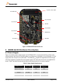
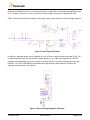
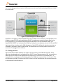
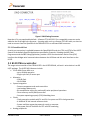
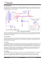
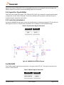
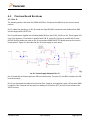
FRDM-KL25Z User's Manual 2013-10-24 Rev. 2.0 Freescale Semiconductor, Inc. FRDMKL25ZUM Table of Contents 1 Overview .....................................................................................................................................................3 2 Reference Documents ............................................................................................................................3 3 Getting Started..........................................................................................................................................3 4 FRDM-KL25Z Hardware Overview ....................................................................................................4 5 FRDM-KL25Z Hardware Description ................................................................................................5 5.1 Power Supply........................................................................................................................................................................ 5 5.2 Serial and Debug Adapter (OpenSDA) ....................................................................................................................... 7 5.2.1 Debug Interface ................................................................................................................................................................................... 8 5.2.2 Virtual Serial Port............................................................................................................................................................................... 9 5.3 KL25Z Microcontroller ..................................................................................................................................................... 9 5.3.1 Clock Source ...................................................................................................................................................................................... 10 5.3.2 USB Interface ..................................................................................................................................................................................... 10 5.3.3 Serial Port ........................................................................................................................................................................................... 10 5.3.4 Reset...................................................................................................................................................................................................... 11 5.3.5 Debug .................................................................................................................................................................................................... 11 5.4 Capacitive Touch Slider ................................................................................................................................................. 12 5.5 3-axis Accelerometer...................................................................................................................................................... 12 5.6 RGB LED............................................................................................................................................................................... 12 5.7 Input/Output Connectors............................................................................................................................................. 13 5.8 Analog Reference Voltage................................................................................................................................................13 5.9 Arduino Compatibility ................................................................................................................................................... 15 Appendix A Revision History..............................................................................................................16 A.1 Changes Between Document Revisions 2 and 1....................................................................................................16 A.2 Previous Board Revisions................................................................................................................................................17 A.2.1 Rev. D...................................................................................................................................................................................................17 FRDMKL25ZUM User's Manual Page 2 of 20 1 Overview The Freescale Freedom development platform is a set of software and hardware tools for evaluation and development. It is ideal for rapid prototyping of microcontroller-based applications. The Freescale Freedom KL25Z hardware, FRDM-KL25Z, is a capable and cost-effective design featuring a Kinetis L series microcontroller, the industry’s first microcontroller built on the ARM® Cortex™-M0+ core. FRDM-KL25Z can be used to evaluate the KL14, KL15, KL24 & KL25 Kinetis L series devices. It features a KL25Z128VLK, a device boasting a max operating frequency of 48MHz, 128KB of flash, a full-speed USB controller, and loads of analog and digital peripherals. The FRDM-KL25Z hardware is form-factor compatible with the Arduino™ R3 pin layout, providing a broad range of expansion board options. The on-board interfaces include an RGB LED, a 3-axis digital accelerometer, and a capacitive touch slider. The FRDM-KL25Z is the first hardware platform to feature the Freescale open standard embedded serial and debug adapter known as OpenSDA. This circuit offers several options for serial communications, flash programming and run-control debugging. 2 Reference Documents The table below provides a list of reference documents for the FRDM-KL25Z hardware. All of these documents are available online at www.freescale.com/FRDM-KL25Z. Table 1. FRDM-KL25Z Reference Documents Filename FRDM-KL25Z Quick Start Package FRDM-KL25Z User’s Manual FRDM-KL25Z Pinouts FRDM-KL25Z Schematics FRDM-KL25Z Design Package OpenSDA User’s Guide Description Quick Start Guide and supporting files for getting started with the FRDM-KL25Z. This document—overview and detailed information for the FRDM-KL25Z hardware. Spreadsheet of pin connections for all MCU pins. Includes pinout for the I/O headers, Arduino R3 compatibility chart, and OpenSDA MCU pinout. PDF schematics for the FRDM-KL25Z hardware. Rev. E and Rev. D available. Zip file containing all design source files for the FRDM-KL25Z hardware. Overview and instructions for use of the OpenSDA embedded debug circuit. 3 Getting Started See the FRDM-KL25Z Quick Start Package for step-by-step instructions for getting started with the FRDM-KL25Z. See the “Jump Start Your Design” section on www.freescale.com/FRDM-KL25Z for the Quick Start Package and software lab guides. FRDMKL25ZUM User's Manual Page 3 of 20 4 FRDM-KL25Z Hardware Overview The features of the FRDM-KL25Z include: • MKL25Z128VLK4 in an 80 LQFP package • Capacitive touch slider • MMA8451Q accelerometer • Tri-color (RGB) LED • Flexible power supply options – USB, coin cell battery, external source • Battery-ready, power-measurement access points • Easy access to MCU I/O via Arduino ™ R3 compatible I/O connectors • Programmable OpenSDA debug interface with multiple applications available including: Mass storage device flash programming interface P&E Debug interface provides run-control debugging and compatibility with IDE tools CMSIS-DAP interface: new ARM standard for embedded debug interface Data logging application Figure 1 shows a block diagram of the FRDM-KL25Z design. The primary components and their placement on the hardware assembly are pointed out in Figure 2. Figure 1. FRDM-KL25Z Block Diagram FRDMKL25ZUM User's Manual Page 4 of 20 Capacitive Touch Slider KL25Z 80 LQFP J10 I/O Header J1 I/O Header RGB LED J9 I/O Header J2 I/O Header MMA8451Q Reset KL25Z USB OpenSDA Figure 2. FRDM-KL25Z Feature Call-outs 5 FRDM-KL25Z Hardware Description 5.1 Power Supply There are multiple power supply options on the FRDM-KL25Z. It can be powered from either of the USB connectors, the VIN pin on the I/O header, an on-board coin cell battery, or an off-board 1.71-3.6V supply from the 3.3V pin on the I/O header. The USB and VIN supplies are regulated on-board using a 3.3V linear regulator to produce the main power supply. The other two sources are not regulated onboard. Table 2 provides the operational details and requirements for the power supplies. Table 2. Power Supply Requirements FRDMKL25ZUM Supply Source Valid Range OpenSDA USB (J7) KL25Z USB (J5) VIN Pin 3.3V Pin Coin Cell Battery 5V 5V 4.3-9V 1.71-3.6V 1.71-3.6V OpenSDA Operational? Yes No No No No User's Manual Regulated onboard? Yes Yes Yes No No Page 5 of 20 Note that the OpenSDA circuit is only operational when a USB cable is connected and supplying power to J7. However, protection circuitry is in place to allow multiple sources to be powered at once. Figure 3 shows the schematic drawing for the power supply inputs and the on-board voltage regulator. Figure 3. Power Supply Schematic In addition, regulated power can be supplied to J3 pin 10 from an external source through P5-9V_VIN by populating the board with an optional voltage regulator, e.g. a 7805 style regulator in a TO-220 package, thus providing a high current supply to external devices. To prevent voltage sag under high load C23, C24, C25 & C28 should be populated with appropriately sized capacitors to match the regulator actually chosen. See Figure 4. Figure 4. Optional Voltage Regulator Schematic. FRDMKL25ZUM User's Manual Page 6 of 20 Table 3. FRDM-KL25Z Power Supplies Power Supply Name P5-9V_VIN P5V_SDA P5V_KL25Z P3V3_VREG P3V3_BATT P3V3 P3V3_KL25Z P3V3_SDA P5V_USB Description Power supplied from the VIN pin of the I/O headers (J9 pin 16). Power supplied from the OpenSDA USB connector (J7). A Schottky diode provides back drive protection. Power supplied from the KL25Z USB connector (J5). A Schottky diode provides back drive protection. Regulated 3.3V supply. Sources power to the P3V3 supply rail with an optional back drive protection Schottky diode. 1,3 Coin cell battery supply voltage. Sources power to the P3V3 supply rail with the option of adding a back drive protection Schottky diode.4 Main supply rail for the FRDM-KL25Z assembly. May be sourced from P3V3_VREG, P3V3_BATT, or directly from the I/O headers (J9 pin 8) KL25Z MCU supply. Header J4 provides a convenient means for energy consumption measurements. 2 OpenSDA circuit supply. Header J3 provides a convenient means for energy consumption measurements. 2 Nominal 5V supplied to the I/O headers (J9 pin 10). Sourced from either the P5V_KL25Z or P5V_OSDA supply through a back drive protection Schottky diode. NOTES: 1) By default the linear regulator, U1, is a 3.3V output regulator. However, this is a common footprint that would allow the user to modify the assembly to utilize an alternative device such as a 1.8V or 2.5V regulator. The KL25Z microcontroller has an operating range of 1.71V to 3.6V. 2) J3 and J4 are not populated by default. The two pins of these headers are in parallel with 0 Ω resistors. In addition, J4 is also in parallel with a 10 Ω resistor. To measure the energy consumption of the KL25Z, either a voltmeter or an ammeter may be used. To use a voltmeter, R73 (0 Ω) must be removed before connecting the voltmeter probes to the pins of J4. Both R73 and R81 (10 Ω) must be removed to measure current with an ammeter. For the OpenSDA MCU, energy consumption can be measured by removing R74 (0 Ω) and connecting ammeter probes to the pins of J3. 3) D12 is bypassed by J20. By default, the pins of J20 are shorted together, to reduce the voltage drop across D12. To use D12, cut the trace between the pins of J20. 4) If a coin cell battery is to be used add a small amount of solder to the coin cell ground pad before adding the battery holder. Also, it is recommended to populate D7 as a protection diode when using a coin cell battery. 5.2 Serial and Debug Adapter (OpenSDA) OpenSDA is an open-standard serial and debug adapter. It bridges serial and debug communications between a USB host and an embedded target processor as shown in Figure 5. The hardware circuit is based on a Freescale Kinetis K20 family microcontroller (MCU) with 128 KB of embedded flash and an integrated USB controller. OpenSDA features a mass storage device (MSD) bootloader, which provides a quick and easy mechanism for loading different OpenSDA Applications such as flash programmers, FRDMKL25ZUM User's Manual Page 7 of 20 run-control debug interfaces, serial-to-USB converters, and more. Refer to the OpenSDA User’s Guide for more details. Figure 5. OpenSDA High-Level Block Diagram OpenSDA is managed by a Kinetis K20 MCU built on the ARM® Cortex™-M4 core. The OpenSDA circuit includes a status LED (D4) and a pushbutton (SW1). The pushbutton asserts the Reset signal to the KL25Z target MCU. It can also be used to place the OpenSDA circuit into Bootloader mode. The OpenSDA MCU RESET can be isolated from SW1 by cutting the trace between pins on J14. SPI and GPIO signals provide an interface to the SWD debug port of the KL25Z. Additionally, signal connections are available to implement a UART serial channel. The OpenSDA circuit receives power when the USB connector J7 is plugged into a USB host. 5.2.1 Debug Interface Signals with SPI and GPIO capability are used to connect directly to the SWD of the KL25Z. These signals are also brought out to a standard 10-pin (0.05”) Cortex Debug connector (J6). It is possible to isolate the KL25Z MCU from the OpenSDA circuit and use J6 to connect to an off-board MCU. To accomplish this, cut the trace on the bottom side of the PCB that connects J11 pin 1 to J11 pin 2. This will disconnect the SWD_CLK pin to the KL25Z so that it will not interfere with the communications to an off-board MCU connected to J6. FRDMKL25ZUM User's Manual Page 8 of 20 Figure 6. SWD Debug Connector Note that J6 is not-populated by default. A Samtec FTSH-105-02-F-D or compatible connector can be added to the J6 through-hole connector. A mating cable, such as a Samtec FFSD IDC cable, can then be used to connect from the OpenSDA of the FRDM-KL25Z to an off-board SWD connector. 5.2.2 Virtual Serial Port A serial port connection is available between the OpenSDA MCU and pins PTA1 and PTA2 of the KL25Z. Several of the default OpenSDA Applications provided by Freescale, including the MSD Flash Programmer and the P&E Debug Application, provide a USB Communications Device Class (CDC) interface that bridges serial communications between the USB host and this serial interface on the KL25Z. 5.3 KL25Z Microcontroller The target microcontroller of the FRDM-KL25Z is the KL25Z128VLK4, a Kinetis L series device in an 80 LQFP package. The KL25Z MCU features include: • 32-bit ARM Cortex-M0+ core up to 48 MHz operation Single-cycle fast I/O access port • Memories 128 KB flash 16 KB SRAM • System integration Power management and mode controllers Low-leakage wakeup unit Bit manipulation engine for read-modify-write peripheral operations Direct memory access (DMA) controller Computer operating properly (COP) Watchdog timer • Clocks Clock generation module with FLL and PLL for system and CPU clock generation 4 MHz and 32 kHz internal reference clock System oscillator supporting external crystal or resonator Low-power 1kHz RC oscillator for RTC and COP watchdog • Analog peripherals FRDMKL25ZUM User's Manual Page 9 of 20 • • • 16-bit SAR ADC w/ DMA support 12-bit DAC w/ DMA support High speed comparator Communication peripherals Two 8-bit Serial Peripheral Interfaces (SPI) USB dual-role controller with built-in FS/LS transceiver USB voltage regulator Two I2C modules One low-power UART and two standard UART modules Timers One 6-channel Timer/PWM module Two 2-channel Timer/PWM modules 2-channel Periodic Interrupt Timer (PIT) Real time clock (RTC) Low-power Timer (LPTMR) System tick timer Human-Machine Interfaces (HMI) General purpose input/output controller Capacitive touch sense input interface hardware module 5.3.1 Clock Source The Kinetis KL25 microcontrollers feature an on-chip oscillator compatible with three ranges of input crystal or resonator frequencies: 32-40 kHz (low freq. mode), 3-8 MHz (high freq. mode, low range) and 8-32 MHz (high freq. mode, high range). The KL25Z128 on the FRDM-KL25Z is clocked from an 8 MHz crystal. FRDMKL25ZUM User's Manual Page 10 of 20 5.3.2 USB Interface The Kinetis KL25 microcontrollers feature a dual-role USB controller with on-chip full-speed and lowspeed transceivers. The USB interface on the FRDM-KL25Z is configured as a full-speed USB device. J5 is the USB connector for this interface. Figure 7. USB Connector Schematic In order to enable USB host functionality on the FRDM-KL25Z, it is necessary to populate J21 and R82 as shown in the figure above. However, there is no electrical protection provided. Use the USB host functionality at your own risk. 5.3.3 Serial Port The primary serial port interface signals are PTA1 and PTA2. These signals are connected to both the OpenSDA and to the J1 I/O connector. Note that the OpenSDA connection can be isolated from J1 by removing R5 & R6, if required. 5.3.4 Reset The PTA20/RESET signal on the KL25Z128 is connected externally to a pushbutton, SW1, and also to the OpenSDA circuit. However, J14 has been provided to isolate the OpenSDA MCU from SW1. Isolating the RESET line allows a more accurate measurement of the target device’s power consumption in lowpower modes. The reset button can be used to force an external reset event in the target MCU. The reset button can also be used to force the OpenSDA circuit into bootloader mode. See section 5.2, Serial and Debug Adapter (OpenSDA), for more details. 5.3.5 Debug The sole debug interface on all Kinetis L Series devices is a Serial Wire Debug (SWD) port. The primary controller of this interface on the FRDM-KL25Z is the onboard OpenSDA circuit (see section 5.2). However, an unpopulated 10-pin (0.05”) Cortex Debug connector, J6, provides access to the SWD FRDMKL25ZUM User's Manual Page 11 of 20 signals. The Samtec FTSH-105-02-F-D or compatible connector can be added to the J6 through-hole debug connector to allow for an external debug cable to be connected. 5.4 Capacitive Touch Slider Two Touch Sense Input (TSI) signals, TSI0_CH9 and TSI0_CH10, are connected to capacitive electrodes configured as a touch slider. Freescale’s Touch Sense Software (TSS) provides a software library for implementing the capacitive touch slider. 5.5 3-axis Accelerometer A Freescale MMA8451Q low-power, three-axis accelerometer is interfaced through an I2C bus and two GPIO signals as shown in Table 4 below. By default, the I2C address is 0x1D (SA0 pulled high). Table 4. Accelerometer Signal Connections MMA8451Q SCL SDA INT1 INT2 KL25Z128 PTE24 PTE25 PTA14 PTA15 Figure 8. MMA8451Q Schematic Diagram 5.6 RGB LED Three PWM-capable signals are connected to a red, green, blue LED, D3. The signal connections are shown in Table 5 below. Table 5. RGB LED Signal Connections RGB LED Red Cathode Green Cathode Blue Cathode FRDMKL25ZUM KL25Z128 PTB18 PTB19 PTD1 1 User's Manual Page 12 of 20 NOTE: 1) PTD1 is also connected to the I/O header on J2 pin 10 (also known as D13). Figure 9. RGB LED Schematic Diagram 5.7 Input/Output Connectors The KL25Z128VLK4 microcontroller is packaged in an 80-pin LQFP. Some pins are utilized in on-board circuitry, but many are directly connected to one of four I/O headers. The pins on the KL25Z microcontroller are named for their general purpose input/output port pin function. For example, the 1st pin on Port A is referred to as PTA1. The I/O connector pin names are given the same name as the KL25Z pin connected to it, where applicable. FRDMKL25ZUM User's Manual Page 13 of 20 Note that all pinout data is available in spreadsheet format in FRDM-KL25Z Pinouts. See the Reference Documents section for details. 5.8 Analog Reference Voltage The onboard ADC of the KL25Z128VLK4 MCU uses the Reference Voltage High (VREFH) and Reference Voltage Low (VREFL) pins to set high and low voltage references for the analog modules. On the FRDMKL25Z, by default VREFH is attached to P3V3_KL25Z (3.3V Supply). VREFL is connected to GND. Figure 10 illustrates this circuitry. FRDMKL25ZUM User's Manual Page 14 of 20 Figure 10. FRDM-KL25Z VREFH Circuit Schematic If desired, VREFH can use a VDDA independent reference by adding R77 and a Zener diode (D9). R80 (0 Ω resistor) must be removed when implementing this option. Alternatively, VREFH can be attached to an external source through AREF by removing R80 and populating R3 with a 0 Ω resistor. 5.9 Arduino Compatibility The I/O headers on the FRDM-KL25Z are arranged to allow compatibility with peripheral boards (known as shields) that connect to Arduino™ and Arduino-compatible microcontroller boards. The outer rows of pins (the even numbered pins) on the headers share the same mechanical spacing and placement as the I/O headers on the Arduino Revision 3 (R3) standard. FRDMKL25ZUM User's Manual Page 15 of 20 Refer to the FRDM-KL25Z Pinouts spreadsheet for a compatibility chart showing how all the functions of the KL25Z signals on the I/O connectors map to the pin functions available on the Arduino Uno R3. FRDMKL25ZUM User's Manual Page 16 of 20 Appendix A Revision History This appendix describes correction to this user’s manual for convenience. Grammatical and formatting changes are not listed here unless the meaning of something changed. A.1 Changes Between Document Revisions 2 and 1 Table A-1. Changes between revisions 2 and 1 Chapter Description 1. Overview • Updated devices that the FRDM-KL25Z can be used to evaluate 4. FRDM-KL25Z Hardware Overview • Updated block diagram to reflect Rev. E changes to board. • Updated Power Supply Schematic (Figure 3) for Rev. E board changes. • Updated FRDM-KL25Z Power Supplies (Table 3) to reflect, and describe Rev. E board changes. Updated Serial and Debug Adapter (OpenSDA) description (5.2) to reflect Rev. E board changes. Updated USB Interface (5.3.2) to include USB Connector schematic and describe the host function configuration. Updated Reset (5.3.4) to discuss OpenSDA MCU isolation from SW1 & RESET line. Added Analog Ref. Voltage (5.8) to describe Rev. E board changes to VREFH. 5. FRDM-KL25Z Hardware Description • • • • FRDMKL25ZUM User's Manual Page 17 of 20 A.2 Previous Board Revisions A.2.1 Rev. D The following section illustrates the FRDM-KL25Z Rev. D features that differ from the current board revision. Rev. E added J14; therefore, on Rev. D boards the OpenSDA MCU cannot be easily isolated from SW1 and the target MCU’s RESET line. Rev. D board power supplies lack a Shottky diode (D10) on the P5-9V_VIN line to U1, J20 to bypass D12 from 3.3V regulator, 0 Ω resistors in parallel with J3 & J4, and a 10 Ω resistor in parallel with J4. Also, BAT54C Shottky diodes are used on Rev. D compared to MBR120VLSFT1G diodes used on the current board revision. Figure A-1 describes the Rev. D power supply in more detail. ure A-1. Power Supply Schematic Rev. D. Fig Rev. D boards do not feature optional USB host functionality. They lack J21 and R82, necessary for USB host functionality. Rev. E has eliminated the solder short found on Rev. D boards, and replaced it with a 0 Ω resistor (R80). In addition, Rev. D boards lack the option of adding a 1 KΩ resistor (R77) and a 3V Zener diode to the VREFH circuitry. FRDMKL25ZUM User's Manual Page 18 of 20 Figure A-2. FRDM-KL25Z VREFH Schematic Rev. D. FRDMKL25ZUM User's Manual Page 19 of 20 How to Reach Us: Information in this document is provided solely to enable system and software Home Page: freescale.com implementers to use Freescale products. There are no express or implied copyright Web Support: freescale.com/support information in this document. licenses granted hereunder to design or fabricate any integrated circuits based on the Freescale reserves the right to make changes without further notice to any products herein. Freescale makes no warranty, representation, or guarantee regarding the suitability of its products for any particular purpose, nor does Freescale assume any liability arising out of the application or use of any product or circuit, and specifically disclaims any and all liability, including without limitation consequential or incidental damages. “Typical” parameters that may be provided in Freescale data sheets and/or specifications can and do vary in different applications, and actual performance may vary over time. All operating parameters, including “typicals,” must be validated for each customer application by customer’s technical experts. Freescale does not convey any license under its patent rights nor the rights of others. Freescale sells products pursuant to standard terms and conditions of sale, which can be found at the following address: freescale.com/SalesTermsandConditions. Freescale, the Freescale logo, and Kinetis are trademarks of Freescale Semiconductor, Inc., Reg. U.S. Pat. & Tm. Off. ARM is the registered trademark of ARM Limited. ARM Cortex-M0+ is the trademark of ARM Limited. All other product or service names are the property of their respective owners. © 2013 Freescale Semiconductor, Inc. Document Number: FRDMKL25ZUM Rev. 2.0 10/2013