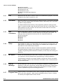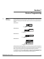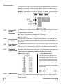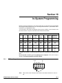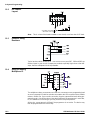
1
STK200 Starter Kit
User Guide
----------------------------------------------------------------
May 2004
R
Table of Contents
Section 1
Introduction ........................................................................................... 1-1
1.1
Device Support .........................................................................................1-1
Section 2
Getting Started...................................................................................... 2-1
2.1
2.2
Unpacking the System ..............................................................................2-1
System Requirements...............................................................................2-1
Section 3
Connecting the Hardware ..................................................................... 3-1
Section 4
Hardware Description ........................................................................... 4-1
4.1
4.2
Jumpers and Links and their Functions ....................................................4-2
External Connections ................................................................................4-2
Section 5
Installing the Software .......................................................................... 5-1
5.1
5.2
Windows 95/98...........................................................................................5-1
Windows NT/2000/ME/XP..........................................................................5-1
Section 6
How to use the Software....................................................................... 6-1
6.1
6.2
6.3
6.4
6.5
6.6
6.7
6.8
6.9
6.10
6.11
6.12
6.13
6.14
6.15
6.16
Projects .....................................................................................................6-1
Files ..........................................................................................................6-1
Editing Data ..............................................................................................6-2
Programming ............................................................................................6-2
Auto-Program............................................................................................6-2
Reloading Projects.....................................................................................6-3
Open Project .............................................................................................6-3
Save Project..............................................................................................6-3
Load File ...................................................................................................6-3
Save File ...................................................................................................6-3
Exit ............................................................................................................6-4
View Menu.................................................................................................6-4
CRC Checksums.......................................................................................6-4
Setup..........................................................................................................6-4
ISP Speed.................................................................................................6-4
Pop Up Warnings......................................................................................6-4
i
Table of Contents
6.17
6.18
6.19
6.20
6.21
6.22
6.23
6.24
6.25
6.26
6.27
6.28
6.29
6.30
6.31
Program Flash ..........................................................................................6-4
Verify Flash .............................................................................................6-5
Program EEPROM...................................................................................6-5
Verify EEPROM ........................................................................ .............6-5
Read Flash.. ............................................................................................6-5
Read EEPROM........................................................................................6-6
Read Fuses .............................................................................................6-6
Read RC Calibration Byte........................................................................6-6
Copy RC Calibration Byte.........................................................................6-6
Program Fuses........................................................................................6-6
Program Lockbits.....................................................................................6-7
Run...........................................................................................................6-7
Erase......................................................................................... ..............6-7
Serial Numbers........................................................................................6-7
Help Menu................................................................................................6-7
Section 7
Device Programming ............................................................................ 7-1
7.1
7.2
7.3
7.4
Device Orientation ....................................................................................7-1
Voltage Selection ......................................................................................7-2
Power and Lead Connections ...................................................................7-2
Programming 8-Pin Parts..........................................................................7-2
Section 8
Brown-Out Detector .............................................................................. 8-1
Section 9
Board Applications................................................................................ 9-1
9.1
Using Switches and LEDs.........................................................................9-1
9.1.1
9.2
9.3
Configuring Switches and LEDs ...............................................................9-1
Using External Connections......................................................................9-1
9.3.1
20-Pin and 40-Pin Digital Sockets ......................................................9-2
9.3.2
40-Pin Analog Socket...........................................................................9-2
9.3.3
28-Pin Analog Socket...........................................................................9-2
9.3.4
20-Pin Analog Socket..........................................................................9-2
9.3.5
8-Pin Socket ......................................................................................9-2
9.3.6
All Sockets..........................................................................................9-2
9.4
Using Analog Parts ...................................................................................9-2
9.4.1
Using Internal Reference....................................................................9-3
9.4.2
Using External Reference...................................................................9-3
9.5
ii
Using 8-Pin Devices with LEDs ..........................................................9-1
Using External Memory.............................................................................9-3
9.5.1
FlashRAM and EEPROM....................................................................9-3
9.5.2
Address Latch.....................................................................................9-3
Table of Contents
9.6
9.7
Using LCD Connections............................................................................9-4
Using RS232 .............................................................................................9-4
Section 10
In-System Programming ..................................................................... 10-1
10.1
10.2
10.3
10.4
ISP Lead Layout .....................................................................................10-1
ISP Header Layout..................................................................................10-2
Interface Using Resistors ........................................................................10-2
Using an Analog Multiplexer IC...............................................................10-2
Section 11
Technical Support............................................................................... 11-1
11.1 Contacting Kanda....................................................................................11-1
Section 12
Socket Support.................................................................................. 12-1
iii
Section 1
Introduction
Welcome to the STK200 Flash MCU Starter Kit.
This system incorporates a sophisticated applications board, Kanda AVR® ISP software
and an ISP dongle that will program any Atmel AVR microcontroller.
1.1
Device Support
The system software (ISP) currently has support for the following Atmel devices.
AVR Devices:
■ AT90S1200, AT90S2313, AT90S2323, AT90S2343, AT90S4434
■
AT90S4414, AT90S8535, AT90S8515
■
ATtiny12, ATtiny15,ATtiny22, ATtiny26
■
ATmega8, ATmega8515, ATmega8535, ATmega48, ATmega88, ATmega168
■
ATmega16, ATmega161, ATmega163
■
ATmeg32
■
ATmega162
■
ATmega64, ATmega128, ATmega169 - no socket support, see STK300
Software upgrades for the AVR ISP software are available from [email protected]
STK200 Starter Kit User Guide
1-1
Section 2
Getting Started
2.1
2.2
Unpacking the
System
System
Requirements
STK200 Starter Kit User Guide
Contents of box:
■ Evaluation Board
■
Software on CD
■
In-System Programming (ISP) Dongle
■
ISP Ribbon Cable
■
AVR Microcontroller
The minimum hardware and software requirements are:
■ 80386 Processor (486 Recommended)
■
1MB Ram
■
1MB Free Hard Disk Space
■
Windows 95
2-1
Section 3
Connecting the Hardware
CONNECT LEAD
SUPPLIED TO DONGLE
AND INSERT IN
PC PRINTER PORT
PLUG HEADER ON LEAD
INTO PROGRAMMING
INTERFACE - KEY WAY
GIVES ORIENTATION
POWER SUPPLY
9 - 15V DC
7 - 12V AC
ON-OFF SWITCH
A power supply is required with a standard 2.1mm barrel connector. It can be AC (7 12V) or DC (9 - 15V). The connector is inserted into the power connection socket as
shown above.
The programming lead supplied is fitted into the Dongle case and the other end is
inserted into the programming interface on the board as shown.
The Dongle case is connected to one of the printer ports on the PC. If this is not LPT1,
then you will need to change the printer port setting in the software—see software section for details.
STK200 Starter Kit User Guide
3-1
Section 4
Hardware Description
Analog Reference
Voltage Adjustment
28A Socket
20A Analog socket
28A Clock Select
EEPROM Socket
Analog Header
LCD Connector
External
SRAM Socket
Port E
Address Decoder
IC for RAM
Port A
Clock Select
20 A Socket
40 pin Digital
Clock Select
20 D Socket
40-pin Analog
ISP
Interface
Port C
Clock Select
8D Socket
Port B 8D and 20
D sockets
8-pin socket
8MHz
Crystal
Port B
20D socket
Port B – 28 A
socket
RS232
3.3V or 5V
Power Input
9-15V DC or
7-12V AC
Port D - All Parts
On-Off Switch
Brownout
2.9V or 4.5V
Power On
Light
ISP Light
8-way Bar
LED
default on
Port B
8 switches
default on Port B
Note: There are a number of jumpers on the board, which are used to select different operations and voltages. The
default jumper settings are for programming operations at 5V. To carry out other operations, some jumpers may have
to be removed - refer to the relevant section for details. A full list of the jumpers and links is given in Section 4.1.
STK200 Starter Kit User Guide
4- 1
Hardware Description
4.1
Jumpers and
links and their
functions
The two jumpers JP1 and JP2 must be either set to both closed or both open for the
board voltage and brown-out to work correcly. Note this behavior is different from
older STK200 versions.
Devices with less than 40-pins have the facility to set an Internal Clock (using programming fuses). If an Internal Clock is used, the External Clock supplied to the
smaller sockets can be disconnected using C/P1..C/P4 jumpers and the port pin can
then be used for normal port I/O.
These CLK jumpers must be set to CLK for Programming operations.
4.2
External
Connections
All Ports are brought out to edge of board on to headers. Each header has a VCC and
Ground pin for power supply to external circuits. The external load cannot exceed 100
mA for all headers combined.
Port A, Port C and Port D headers are connected to all sockets which have those
ports available.
Port E is a replacement for the Misc Header on older STK200 versions as 40-pin
Digital ATmega devices now have port E. Note that the alternate functions of these
pins are now wired to Port E0..2
Port B has 3 headers for different Sockets as the programming connections use different pins on Port B on different devices.
Port B header is for 40-pin sockets (40A and 40D) and the 20-pin Digital Socket
(20D). Note: older STK200 code can use this header for all sockets for code compatibility.
Port B (20A/8D) header routes signals correctly for the 20-pin Analog socket and the
8-pin Digital socket - labelled 20D and 8D.
Port B (28A) header routes signals correctly for the 28-pin Analog socket - labelled
28A.
See “Using External Connections” in Section 9-1 and “Using Analog Parts” in Section
9-3 for details.
4-2
STK200 Starter Kit User Guide
Section 5
Installing the Software
5.1
Windows 95/
Windows 98
Insert the CD supplied into your CD Drive.
Open explorer and select your CD Drive.
Each program supplied has its own folder and is installed separately.
To install ISP software, select AVRISP folder and double click on the .exe file.
To install AVR Studio, select AVR Studio folder and double click on astudio4.exe
To install Application Builder, select application builder folder and double click on .exe
file
Manuals, schematics, sample programs, device datasheets etc. can be read from the
CD or copied to your hard drive
5.2
Windows NT
Windows 2000
Windows ME
Windows XP
Insert the CD supplied into your CD Drive.
Open explorer and select your CD Drive.
Each program supplied has its own folder and is installed separately.
To install ISP software, select AVRISP folder and double click on the .exe file.
To install AVR Studio, select AVR Studio folder and double click on astudio4.exe
To install Application Builder, select application builder folder and double click on .exe
file
Manuals, schematics, sample programs, device datasheets etc. can be read from the
CD or copied to your hard drive
You must make sure that you have Administrator priviledges to install the software
STK200 Starter Kit User Guide
5- 1
Section 6
How to use the Software
The software is fully context-sensitive. This means that pressing F1 at any time will bring
up help information about the current option that you have selected.
Please note that the toolbar icons referred to in the text have ToolTip’s. If you want to
know the function of any particular button, hold your mouse pointer over the button in
question and its function will be displayed.
■ Starting a Project
■
In-System Programming (ISP)
■
Hardware Requirements
■
Projects
■
Data Files
■
Editing Data
6.1
Projects
If you have used a high-end professional development system, you will be familiar with
the project concept. Essentially, this is a collection of information which is managed by
the program on your behalf. In the AVR you have both Program Memory and non-volatile Data Memory (EEPROM), and you have various security and device options. The
project manager keeps this information together for you so you do not have to remember and reload all of the files every time you use the programmer.
It will also allow you to store information, such as the project name and the project identifier. Also included is a small notepad to store comments about the project.
You do not need to use projects if you do not want to. Just change device and load Flash
and EEPROM buffers separately. You will also need to check Fuse and Lockbit settings.
If you do want to use Prohjects, the "Load Project Settings" and "Save Project Settings"
menu choices are in File Menu.
6.2
Files
Either open a project or you can load the files that you want to program into the device.
Files are loaded by either using the “Load” command in the File menu or by using
the “Open”hot keys - CTRL-O for Flash and CTRL-ALT-O for EEPROM.
The program will automatically decode your files whether they are in Intel Hex format,
Atmel Generic, Binary, or Motorola S record. The file you choose will be loaded into the
window, then will be displayed on the top of the desktop. If you have the EEPROM Data
Memory window on top, then it will load the data into that window.
STK200 Starter Kit User Guide
6-1
How to use the Software
Note that the AVR Studio which accompanies this program will produce the correct
files for you ready to load into the buffers. You can save the buffer in Binary, Intel Hex,
or Atmel Generic formats, so you can use the buffer for code conversion.
Similarly, it will load the data into the Program Memory if that is the window that is on
top. The program will not allow you to load data if the project manager window is on top.
To change which window is on top, you can either click your mouse on any part of the
window that is showing, go to the “Window” menu using Alt-W or the mouse and select
the window of your choice, or press Ctrl-F6. Note that the loaded data will show up in
blue text where the default, empty text color is black.
Once your data files are loaded you can start your programming session.
6.3
Editing Data
Once a project has been started, you can either load a data file or you can insert your
own data in Hex or ASCII directly into the Program or EEPROM data windows.
With a new project, the data windows called buffers will contain FF in every location.
This is also what a new or erased device will contain.
You can move around in the current window by using the cursor keys. In order to see
memory further down the window, use the “Page Up” and “Page Down” keys on the keyboard.
You may change the data at any memory location by clicking on that location and typing
in the required hex values. Any changes you make will be reflected by the data changing
to green text. The ASCII character of the hex value will be shown alongside the data
window.
If you wish to edit the buffer in ASCII, click on the right area of the window.
Once you have entered the required data, then you can save the contents of the current
buffer, either Flash or EEPROM by choosing "Save" from the File Menu and selecting
Flash or EEPROM.
6.4
Programming
Read the section on “Device Programming” in section 7-1 or “In-System Programming”
in Section 10-1 before programming parts.
Before you can start programming a device you must have a project or file open on the
desktop.
6.5
Auto-Program
The easiest and quickest method of programming a device is to use the “Auto-Program”
option which is available in either the “Device” menu or by using the hot key which
is F5. Before you use this option, select Auto-Program Options which gives a list of
check boxes to select which features you want to enable or disable during the programming session. You can enable or disable any of the options by clicking on them or using
“Arrow” and “Space” keys. If the option has a check mark next to it, then it is enabled, if
not, then it is disabled. Note that the default is for all the options to be disabled. Further
note that you should not disable the erase function under normal circumstances.
If the Dongle is not plugged into your printer port, you may get an error. If you get the
“Dongle Not Found” error and it has been inserted into the printer port, make sure that
you have selected the correct printer port. You can change the printer port setting by
clicking on Setup button and choosing a different printer port (if available) from the
drop down list.
The programmer then attempts to read the device signature bytes. If they are not found
because you are using an old version of the device, no device is plugged in, the module
is switched off or the lock bits are set, a message box informs you of this. You have the
option of Abort, Retry or Ignore.
6-2
STK200 Starter Kit User Guide
How to use the Software
Once you have set the Auto Program Options, pressing F5 or selecting Auto Program
from the Device menu will carry out those operations. These operations can also be
selected individually, except Increment Serial Number.
l Reload Files
l Read EEPROM
l Erase device
l Program and Verify Flash
l Program and Verify EEPROM
l Program and Verify Fuses
l Program and Verify Lockbits
l Increment Serial Number
l Copy RC Calibration Byte
l Run
Note: The programmer holds the target in Reset, so select Run if you want your code
to run
6.6
Reloading
Projects
Older versions of AVR ISP saved Project settings in the registry, which made it difficult
to change computer. Select Input Old AVR Projects from the File menu to re-use older
style projects
6.7
Open Project
Select “Load Project Settings” from the File menu to reopen projects that have been
previously saved using Save Project Settings. Projects saved using earlier versions of
AVR ISP should be loaded using Input Old AVR Projects command.
6.8
Save Project
To save your current File, device and Fuse settings, select “Save Project Settings”
from the File menu.
6.9
Load Files
To load data into the Flash and EEPROM Buffers, select Load from the File menu.
Then select Flash or EEPROM to load a file into the correct buffer. Or use the hot
keys CTRL-O to load Flash and CTRL-ALT-O to load EEPROM.
If the file is too big for the selected device memory, the file will still be loaded but will
appear in red and the Status Line gives a warning.
The File Load will detect the file format and automatically load it. The load function will
check for different file types. If no type is detected, the file will be loaded as binary
data.
Supported file types
l Intel Hex (3 types)
l Motorola S-Record (3 types)
l Atmel Generic 8-bit
l Atmel Generic 16-bit
l Tektronics and Extended Tektronics
l Binary
or use Auto Detect.
6.10
Save Files
Select Save from the File menu and then select Flash or EEPROM. Select the format
in which to save the data in the buffer. This save function can be used to convert to
different file types.
Data can be saved in the following formats:
6-3
STK200 Starter Kit User Guide
How to use the Software
l
l
l
l
l
l
Intel Hex (3 types)
Motorola S-Record (3 types)
Atmel Generic 8-bit
Atmel Generic 16-bit
TeKtronics and Extended Tektronics
Binary
6.11
Exit
Select Exit from File menu or click on close icon to shutdown the program. You will be
prompted to save files if a project is in use.
6.12
View Menu
This menu allows you to swap between the different windows - Flash Buffer, EEPROM
Buffer, Fuse and Lockbits window and Status window. Alternatively click on the different tabs to change windows.
The Status Window keeps a history of the programming session including all messages. To clear the window, right click with the mouse and click on Clear Status. The
Status Window can also be saved. This menu also contains other view functions,
described in the next sections.
6.13
CRC
Checksums
Select in View menu. A dialog box appears giving checksum values for the whole
Flash and EEPROM buffers, as well as values for the used part of the buffers. The
CRC type can be changed from the drop down list. Suported formats are
l CRC-16 Standard
l CRC-16 CCITT
l CRC-32
l XOR-16
l XOR-32
6.14
Setup
Also available as a button, the Setup dialog box can be found in the View menu. The
main function is to change the current printer port. Available ports will appear in the
drop down list. Just choose the port required.
Also available are advanced settings for different programmer speeds and delays.
ISP speed should be changed if you experience time out problems or use a slow
oscillator. Programming times should be increased if you find verify errors during programming
6.15
ISP Speed
Found in the Setup dialog box (View menu or button). ISP speed should be changed if
you experience time-out problems during programming or verifying operations.
It should also be changed if your target oscillator is slower than normal. The fastest
speed is for 8MHz or above, and the slowest is for 32KHz. Choice a value that does
not give timeout errors.
Pop Up Warnings in the view menu can be enabled or disabled. If enabled, a programming or verify error will pop up a warning dialog box that must be closed before
another programming operation can take place. This feature is included to make it
harder for operators to ignore errors during production.
6.16
Pop Up
Warnings
6.17
Program Flash Program (Flash) is in the Device menu. Click on Program and select which part of the
device you want to program - Flash memory, EEPROM memory, Fuses or Lockbits.
The hot key for Program Flash is CTRL-ALT-F6.
6-4
STK200 Starter Kit User Guide
How to use the Software
This option programs and verifies each location from the selected buffer window into
the appropriate location in the device.
Note: It is advisable to erase the device before programming unless you are adding
extra data to existing data in the device.
If you are changing data, then you cannot change any programmed bit from a 0
to a 1 without erasing the device first. You can, however, change a bit from a 1
to a 0. For example, BB could be changed to AA but AA cannot be changed to
BB. You will not be able to program the device if the write lockbit has been set.
If this function is selected from the “Program” menu, it will only program the Flash
Memory. In devices which also have EEPROM Memory available, you must use the
“Program EEPROM” command.
6.18
Verify Flash
Choose Verify from the Device Menu and then select Flash. Or press F6. The data in
each location in the Flash buffer is compared with the data in the device. If all the data
is the same, the buffer will show green lettering. If a verify error occurs, then those
locations will go red and a message will appear, giving the location of the first error.
6.19
Program
EEPROM
Choose Program from the Device menu, then select EEPROM. The hot key is CTRLALT-F7.
The EEPROM can be re-programmed without a previous erase command, unlike the
Flash memory. If the Lockbits are set however, the device must be erased first.
6.20
Verify
EEPROM
Choose Verify from the Device Menu and then select EEPROM. Or press F7. The
data in each location in the EEPROM buffer is compared with the data in the device. If
all the data is the same, the buffer will show green lettering. If a verify error occurs,
then those locations will go red and a message will appear, giving the location of the
first error.
6.21
Read Flash
Choose Read from the Device Menu and then select Flash. Or press CTRL-F6. The
data in each location in the Flash memory is uploaded to the Flash Buffer. Any data
already in the buffer will be overwritten.
6.22
Read EEPROM Choose Read from the Device Menu and then select EEPROM. Or press CTRL-F7.
The data in each location in the EEPROM memory is uploaded to the EEPROM
Buffer. Any data already in the buffer will be overwritten.
6.23
Read Fuses
Choose Read from the Device Menu and then select Fuses. Each fuse that is readable is uploaded and displayed on the Fuses screen. Note that Lockbits cannot be
read directlybut if a Flash Read displays sequential repeating numbers, then the
Lockbits are set
6.24
Read RC
Calibration
Byte
Choose Read from the Device Menu and then select RC Calibration Byte. This byte
(or bytes depending on the device) is stored in the device signature space and is used
to calibrate the Internal RC Oscillator on most ATmega devices. This function shows
the values in a dialog box.
Note: The values can only be changed in code, not by the programmer. Please refer
to device datasheets for an appropriate code example.
6.25
Copy RC
Calibration
Byte
Choose Copy RC Calibration from the Device Menu. This byte (or bytes depending on
the device) is stored in the device signature space and is used to calibrate the Internal
RC Oscillator on most ATmega devices. This function copies the values in the device
and you are prompted for a location to store them, either in Flash or EEPROM buffer,
for later study. Note: The values can only be changed in code, not by the programmer. Please refer to device datasheets for an appropriate code example.
6-5
STK200 Starter Kit User Guide
How to use the Software
6.26
Program
Fuses
Select Program from Device Menu, then select Fuses. The current Fuse values that
are set on the Fuses and Lockbits screen are programmed into the device. The available Fuses vary from device to device.
Important Note: AVR devices use a zero value for programmed fuses and a one for
unprogrammed fuses, but the programmer screen ignores this. Therefore, to program
a fuse, check the box next to the fuse and to leave it unprogrammed, do not check the
box. The programmer will program the fuses to the correct values.
Another important note: Be careful with fuse settings or you can lock the device. In
particular, be very careful when changing Clock Select fuses. The STK200 supports
most clock settings except slow speed oscillator, but other target circuits may not support all options. If an unsupported clock type is chosen, you will not be able to enter
ISP.
6.27
Program
Lockbits
Select Program from Device Menu, then select Lockbits. The current Lockbits values
that are set on the Fuses and Lockbits screen are programmed into the device. The
available Lockbits vary from device to device.
All devices have the main device lockbits that can be set to Unlocked, No write or No
read or write. The only way to clear lockbits once they are set is to erase the device.
Lockbits cannot be read.
Devices with a Boot Block have extra lockbits (BLB bits) to restrict access to the Boot
Block area. These bits are also set by the Program Lockbits command.
Note: The Boot Block Size and Reset Vector location are Fuses and are set by the
Program Fuses command.
6.28
Run
Select Run from the Device menu. This command allows user code to run on the target device with the programmer connected. The programmer holds the device in reset
so code cannot run unless this command is used or the programmer is disconnected
from the target system
6.29
Erase
Erase is in the Device menu. Erase will remove all code from the device, in both the
Flash and EEPROM memories. So, if you want to save any data, read the device first
and save the Flash and/or EEPROM buffers to file. Auto Program has an option to
read the EEPROM first and write it back after erase.
Erase is the only way to clear Lockbits if they are set.
Note: In most cases a device must be erased before it is programmed.
6.30
Serial
Numbers
Serial Numbers can be added using this menu command. Serial Numbers can be 2, 3
or 4-byte. The format can be binary, decimal, hexadecimal or octal. Data is stored as
1 number per nibble, so a 4-byte serial number can have 8 digits (or 32 binary bits).
The serial number can be added to the Flash Memory or the EEPROM memory at a
user defined location. Please ensure that your chosen location does not over write
code, that it leaves enough room for your serial number size if it is at the end of memory and it is within the memory size of your chosen device.
The default current serial number can also be set if you do not want to start from zero.
Serial Numbers can be set to auto-increment in Auto Programming Options in the
Device menu, or can be changed manually each time a device is programmed
6-6
STK200 Starter Kit User Guide
How to use the Software
6.31
Help Menu
The Help menu has options for displaying the included Help File or you can press the
F1 key.
The latest readme file can also be opened in the Status Window and there are options
for checking for software updates and other on-line information.
The About dialog box tells you the Version Number of the software you are using. If
you need to contact support or check for updates, note the version number of your
software.
6-7
STK200 Starter Kit User Guide
Section 7
Device Programming
7.1
Device
Orientation
Before programming a device using the programming module, the device must be
inserted correctly into the programming unit. The AVR device has an arrow printed on it,
which points towards pin 1 of the device. Below are the four socket types and their orientation.
8-Pin Devices
PIN 1
20-Pin Devices
PIN 1
28-Pin Devices
28
PIN 1
40-Pin Devices
PIN 1
Another method of checking to see if it is inserted correctly is to check the notches on
both the device and the programming socket. At the end of the device you will notice a
notch cut-out. There is a notch cut-out on the device socket which is also printed on the
board. The notch on the device must correspond with the notch in the socket.
The orientation of the device is vitally important. If you put it in the wrong way then you
may damage the device. Do not plug a device in with the power switched on or you
may damage it. Similarly, never remove the device with the power on.
STK200 Starter Kit User Guide
7-1
Device Programming
40-pin A/D parts have different pinouts from the digital only 40-pin parts. Make sure
you have inserted your device in the correct 40-pin socket on the board. The board
has “40D” and “40A” written inside the sockets.
Note: Do not insert a device in more than one socket at a time otherwise programming errors will occur.
7.2
Voltage
Selection
Jumper JP1 is used to select either 3.3V or 5V programming.
For VCC = 5V, close jumper JP1 – jumper closed
For VCC = 3.3V, remove JP1 – jumper open
Jumper JP2 is used to set Brown-Out detector voltage.
For Brown-Out =4.5V, insert jumper JP2 – jumper closed
For Brown-Out = 2.9V, remove jumper JP2 – jumper open
This should be set to the same voltage as VCC. If VCC is set to 3.3V and Brown-Out
is set to 5V, then the device will be held in reset and will not program. See the section
“Brown-Out Detector” on page 8-1 for more details.
7.3
Power and
Lead
Connections
The 10-way programming lead is inserted in the box header—the key-way ensures
correct orientation. The computer connections are shown in the section “Connecting
the Hardware” on page 3-1.
The power supply 9-15V DC or 7-12V AC is plugged into the power connector 5.5/2.1
Barrel.
The “Power On/Off” switch is located next to the power connector. Insert the device
before switching the power on. The power on LED should light when the power is correctly applied.
Your hardware is now ready for programming. Refer to “How to use the Software” on
page 6-1 for details of programming operations.
7.4
Programming As these parts are only 8-pin, the clock inputs use two of the port pins. These pins
can be used as port pins on some devices if the device is set to run on internal clock.
8-pin Parts
The internal clock is set by programming a fuse but this may not be set on new parts,
so a jumper is supplied to enable the device to be programmed with external clock.
We recommend that the jumper labeled “C/P3” is set to “EXT” when programming
new parts. The fuse setting can then be read and set to internal clock if the port pins
are required, and the jumper setting can then be changed to “PB3” for internal clock
operation.
Note: If the internal clock fuse is set, the internal clock will operate even if an external
clock is supplied.
If difficulties are found in programming these parts, remove the lead from “Port B” to
“LEDs”. (Bits 0 to 2 are the programming lines.)
7-2
STK200 Starter Kit User Guide
Section 8
Brown-Out Detector
The brown-out detector circuit is used to detect voltage drops. If a short glitch occurs in
the power, this circuit ensures that the processor resets properly rather than operating
randomly.
The brown-out detector must be set to the same voltage as the circuit voltage, VCC—
3.3V or 5V. For 3.3V operation, jumper JP2 must be removed (jumper open) and for 5V
operation it must be closed.
Voltage
Operating Voltage
Hysteresis
5 Volts
4.5 Volts
200 mV
3.3 Volts
2.9 Volts
200 mV
These values are approximate and may vary with temperature and other factors.
If the brown-out detector voltage is set to 5V and VCC is set to 3.3V, then the brown-out
circuit will operate continuously and the device will be held in permanent reset. JP1 and
JP2 must be set to the same voltage, which is always both open or both closed.
STK200 Starter Kit User Guide
Voltage
JP1
JP2
5 Volts
Closed
Closed
3.3 Volts
Open
Open
8-1
Section 9
Board Applications
9.1
Using
Switches and
LEDs
The LEDs are connected through a 1K resistor network to LED header. A 10-way lead
connects to a Port header, by default Port B.
The switches are connected to the Switches header. A 10-way lead connects to a Port
header, by default Port D.
The switches and LEDs can be disconnected, if required. To use them, ensure that
the leads are connected. The board is also marked with the port pin connection for
each switch and LED.
9.1.1
Using 8, 20
and 28-pin
devices with
LEDs
The port pins on the 8,20 and 28-pin sockets have different connections for programming (SCK, MISO and MISO are on different pins), so the pins are not connected correctly to the standard Port B header.
Therefore, the are two other Port B headers :
Port B (20A/8D) - for 20-pin analog socket (20A) and 8-pin socket (8D)
Port B (28A) - for 28-pin analog socket (28A)
Standard Port B header is for 40-pin sockets, 28-pin Digital socket and compatibility
for old designs.
So, connect the ribbon cable from LED header to the correct Port B header for the
socket you are using.
9.2
The ports must be correctly set in software as input or output. This is accomplished by
Configuring
Switches and setting the direction control registers to 0 for input and 1 for output. Typical set-up
code would be:
LEDs
ldi r16,$ff ;load immediate into temp storage register
out DDRB,r16 ;PORTB (LED’s) is all outputs
ldi r16,$00 ;load immediate into temp storage register
out PORTB,r16 ;switch all the LEDs on
out DDRD,r16 ;set direction register to zeros for input
9.3
Using External All the ports are brought out to headers on the edge of the board but there are differConnections ences for different sockets which are described separately. Port B has current limit
resistors for programming on Pin 7, Pin 6 and Pin 5 MOSI, MISO and SCK. These
port pins will only supply a reduced current if used as outputs—300 micro Amps @
3.3V and 500 micro Amps @ 5V. As inputs, they will behave normally. Therefore, any
user circuit should use Port B for inputs.
g 28-pin Analog socket – labelled 28A. Port A and Port C are connected to headers
Port A and Port C. Port B is connected to header marked Port B (28A).
g 40-pin Analog socket – labelled 40A. Port A, Port B, Port C and Port D are connected to headers Port A to Port D.
g 40-pin Digital socket – labelled 40D. Port A, Port B, Port C, Port D and Port E are
connected to headers Port A to Port E.
g 20-pin Digital socket - labelled 20D. Port B and Port D are connected to headers
marked “Port B” and “Port D”.
g 20-pin Analog socket - labelled 20A. Port B and Port D are connected to headers
marked “Port B(20A/8D)” and “Port D”. Port B Header is also connected but in wrong
order
g 8-pin socket – labelled 8D. Port B is connected correctly to header Port B (20A/8D)
and in different order to header Port B.
7-2
STK200 Starter Kit User Guide
Board Applications
In addition to the port pins, each header has a connection for ground and VCC to supply external circuits. This voltage VCC will be either 3.3V or 5V depending on the setting of jumper 1 JP1 and the brown-out detector will operate as normal (see “BrownOut Detector” on page 8-1).
Note: If your circuit is to draw significant current >250 mA then a heat sink will be
required on the on-board regulator—LM317. This device is rated at 1.5 Amps
but it needs a heat sink to supply this current. If your circuit will draw more than
1 Amp, you may need a separate power supply.
9.3.1
20-pin and 40- The ports on the 40-pin digital socket are connected to the headers marked “Port A”,
“Port B”, “Port C”, “Port D and “Port E”. The 20-pin socket is connected to the headers
pin Digital
marked “Port B” and “Port D”. The layout of all the headers is the same and is shown
Sockets
in the following diagram.
9.3.2
40-pin Analog This socket is marked 40A. The layout, shown above, applies to Port A, B, Port C and
Port D on these parts. Using ADC is described in section 9.4
socket
9.3.3
28-pin Analog This socket is marked 28A. The layout, shown above, applies to Port B, Port C and
Port D on these parts. Note: Port B is connected to the header marked Port B (28A)
socket
in the correct order, and to Port B header in wrong order. Port B only has six bits, PB0
- PB5. These are connected to the correct header on header Port B (28A) but to bits 2
to 7 on the header marked Port B.
The ADC inputs are on Port C - see section 9.4 for more details,
9.3.4
20-pin Analog This socket is labelled 20A. The layout, shown above, applies to Port B and Port D
on these parts. Note: Port B is connected to the header marked Port B (20A/8d) in
socket
the correct order, and to Port B header in wrong order.
9.3.5
8-pin socket
This socket is labelled 8D. The 8-Pin socket has five Port bits connected: PB0 - PB4.
These are connected to the header marked Port B (20A/8d) in the correct order, and
to Port B header in wrong order. The connections for this socket on the Port B
(20A/8D) header are as shown above.
9.3.6
All sockets
If external operations do not want pull-ups on the port pin, both the switches and the
LEDs can be disconnected from the processor. To isolate the LEDs, or switches,
remove the leads
9.4
Using Analog 40-pin Analog parts must be used in the socket marked “40A”, and 28-pin parts
must be used in the socket marked “28A”. The A/D converters use Port A on the 40Ports
pin A/D socket and Port C on the 28-pin socket. The layout of these headers are
shown above.
9-3
STK200 Starter Kit User Guide
Board Applications
To use the ADC you will need to connect to both the Analog Header and the correct
ADC port for your device (Port C for 28A and Port A for 20A and 40A).
AVCC Pin - separate pin for Analog voltage output - connected to Analog Voltage circuit and AVCC pin on device. Connect to this pin on external circuits that use ADC.
AGND Pin - separate pin for Analog Ground output - connected to Analog Ground circuit and AGND pin on device. Connect to this pin on external circuits that use ADC.
The board has an on-board Voltage Reference, the pot marked “AREF” is used to set
the voltage level if the jumper is connected from POT to EXT pins (28A/40A sockets)
or POT to 20A pins (20A socket).
EXT - EXT pin is connected to AREF pin on the AVR device (28A and 40A sockets).
20A - 20A pin is connected to PA3/AREF pin on 20A socket
POT - Connect jumper from POT to 20A or EXT pin to connect AREF Pot to the
AREF pin of device.
9.4.1
Using AREF
Pot for
Reference
9.4.2
Using External To use the A/D converters with an external Voltage Reference, remove jumper and
apply your own voltage reference to EXT pin for 28A and 40A sockets or 20A pin for
Reference
20A socket.
9.5
Using External The AT90S8515/ATmega8515 can be used with external SRAM. A socket is provided
for a 28-pin FLASH RAM chip and for an address latch chip. These are next to the
Memories
LCD connector on the board. An 8-pin socket is also provided for 24Cxxx EEPRO.M
9.5.1
An Atmel AT29C256 Flash RAM is suggested. If a very fast RAM is required, the crysFlash RAM
and EEPROM tal frequency may need to be increased. Note: On older STK200 boards, this socket was laid out for a 62256 Static RAM chip with different pin-outs.
RAM Socket pin layout
EEPROM Connections
The 8-pin socket near the AREF POT
labelled 24C is for an EEPROM. This
EEPROM type uses a two wire connection (I2C type) with SDA and SCL lines.
These lines can be used with AVR TWI
peripheral or a software routine.
The two communication lines are connected to 28 and 40-pin sockets, to pins
PC0 and PC1.
24C
Pin5
Pin6
9.5.2
Line
SDA
SCL
28A, 40A, 40D sockets
PC1
PC0
Address Latch The board connections are for a 74HC573 device. This device will operate reliably
with the 8 MHz crystal supplied but if a faster crystal is inserted, a faster version of
this device may be required—74AHC573 or 74FHC573. Note that this option will alter
the EMC characteristics of the board.
9-5
STK200 Starter Kit User Guide
Board Applications
9.6
Using LCD
Connector
The header marked LCD next to the 28-pin RAM socket, is for a standard 2 x 16 LCD.
The connections are shown on the board and in the following table.
The board is designed for use with a LCD with a Hitachi driver chip built-in, using a
contrast pin voltage of 0 to 5 Volts. The resistors next to the LCD connector, marked
R22 and R23 are used for contrast adjustment. They form a potential divider and the
default contrast voltage is 0.6V.
This board is not designed for use with back lit LCD modules, so the extra connections needed are not included and the power supply will not supply the current
required.
The LCD can be driven in Memory Mapped or I/O Mode—see data sheet. If the crystal has been changed to a faster crystal frequency, memory mapped operations may
not work.
9.7
9-4
Using RS232
The connection supplied is a 9-way female D-type, therefore a “straight through” lead
is required not a null-modem cable.
RXD and TXD are on pins PD0 and PD1 on most devices. The default connection for
the switches is also Port D. Do not use switches on Port D0 and Port D1 if RS232 is
in use. If communication problems occur, remove the switch lead from Port D.
STK200 Starter Kit User Guide
Section 10
In-System Programming
Devices can be programmed in your circuit rather than on the board using the STK200
ISP dongle that was included in the kit. The dongle works with a 0.1" pitch header that is
mounted on your application board.
You will need to use either a multiplexer chip (such as a 4053), or wire directly to the
pins of the device. The pins on the device are connected as follows:
AVR Device
1200
2313
2323/
2343
4414
8515
8535/
4434
MEGA603/
MEGA103
Reset
Pin1
Pin1
Pin1
Pin9
Pin9
Pin9
Pin20
MOSI
(PDI)
PB5
Pin17
PB5
Pin17
PB0
Pin5
PB5
Pin6
PB5
Pin6
PB5
Pin6
PE0
Pin2
MISO
(PDO
PB6
Pin18
PB6
Pin18
PB1
Pin6
PB6
Pin7
PB6
Pin7
PB6
Pin7
PE1
Pin3
SCK
PB7
Pin19
PB7
Pin19
PB2
Pin7
PB7
Pin8
PB7
Pin8
PB7
Pin8
PB1
Pin11
Pin
In addition, the system +5 Volts and Ground need to be connected to the programming
lead.
Do not exceed 5 volts or you may damage your computer. 4.75 to 5.25 volts is
allowed. This warning applies to any ISP system.
10.1
ISP Lead Layout
Vcc
Ground
MISO
MOSI
SCK
Note:
STK200 Starter Kit User Guide
LED
RST
This is a face view of the ISP lead. Section 10.2 shows connector on user circuit.
10-1
In-System Programming
10.2
ISP Header
Layout
OPTIONAL PROGRAM
INDICATOR CIRCUIT
Note:
10.3
This is a view of the header needed on user circuit, not a face view of ISP lead.
Interface Using
Resistors
Typical resistor values would be 1K. This circuit is fine if ports PB7, PB6 and PB5 are
used as inputs in your circuit. If outputs are needed, especially higher than a few milliamps, then the multiplexed circuit is preferable.
10.4
Using an Analog
Multiplexer IC
The multiplexer select can be driven from the LED connection on the programming lead
as can a low-power LED with its cathode connected to the LED connection via a suitable
resistor—1KΩ is fine. If you use this connection, then the output will be low 0 during programming and a 1 at all other times. Note that it will float if the programmer is not active,
i.e., the software is not running so you may need to use a pull-up resistor.
All the pins, except ground, will float if the programmer is not active. The device may
then be programmed in the normal way.
10-2
STK200 Starter Kit User Guide
Section 11
Technical Support
Technical support for this product is provided by the AVR Starter Kit Support Team.
Contact information is provided below.
11.1
Contacting Kanda We would be grateful if you can report any errors you may find in this software. We pride
ourselves on our customer support. As soon as we are aware of the problem, we can
solve it and send you an update very quickly via e-mail. If you wish to communicate via
telephone, the number is listed below:
Tel:
(44) (0)8707 446 807
Fax:
(44) (0)8707 446 807
e-mail:
[email protected]
Website:
www.kanda.com
We also have an extensive range of AVR development products available. Please visit
our website (http://www.kanda.com) for full details.
Software upgrades will be made available from support
STK200 Starter Kit User Guide
11-1
Section 12
Socket Support
The sockets are labelled by type not by device name to allow for new device support.
Note: The new STK200 has an extra socket for new 20-pin parts such as the
ATtiny26. This is labelled 20A
12.1
Socket
Support
Contact [email protected] for more information.
STK200 Starter Kit User Guide
12- 1