1
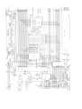
SERVICE
FOR
MANUAL
THE
ORIC-1 and ORIC ATMOS
MICROCOMPUTERS
This version typed and scanned by S D Marshall 2003
www.48katmos.freeuk.com
AMENDMENT RECORD
DATE
AMENDMENT
PAGES
ISSUED
NUMBER
AFFECTED
REMARKS
RELEVANT
MODIFICATION
NUMBER
OR SERVICE
BULLETIN
2
Copyright Oric Products International Limited 1984.
The information contained in this document must not be
reproduced in any form whatsoever without prior written
permission from Oric Products International Limited.
The
product
described
in
this
document
is
subject
to
continuous development and it is acknowledged that there
may be errors or omissions.
Oric
can
accept
no
responsibility
for
such
omissions
and/or errors, nor for damage or loss resulting from work
carried out on the product by persons other than those
authorised
to
do
so,
by
Oric
Products
International
Limited.
Oric
would
suggestions
be
most
from
grateful
users
for
regarding
any
this
comments
document
and/or
or
the
product it describes. All such correspondence and queries
regarding this manual should be sent to:
Customer Services
Oric Products International Limited,
Coworth Park,
London Road,
Ascot,
Berks SL5 7SE.
(Note: Oric closed down some time ago. Addresses printed here are no longer valid and it is assumed this
document can be regarded as copyright free. SDM)
3
This document is for the use of ORIC authorised dealers and
servicing organizations/centres and is NOT for distribution
to the general public.
4
CONTENTS
1. INTRODUCTION
7
2. MODIFICATIONS AND AMENDMENTS
8
3. TECHNICAL DESCRIPTION
10
4. TEST EQUIPMENT
21
5. FAULT FINDING
22
Introduction
22
Disassembly
25
Screen Faults
26
Picture Quality Adjustment
30
Sound Faults
31
Keyboard faults
32
Powering up (initialization) faults
35
Tape Cassette loading faults
38
Waveforms – general
40
6. ORDERING COMPONENTS AND RETURNING ITEMS
5
44
APPENDICES
APPENDIX 1 - PARTS LIST
46
APPENDIX 2 - MODIFICATION LEAFLETS
68
APPENDIX 3 - INTEGRATED CIRCUIT DATA
73
APPENDIX 4 - SERVICE BULLETINS
74
DRAWINGS
77
Main printed circuit board - circuit diagrams
78
Keyboard
79
- circuit diagrams
6
1. INTRODUCTION
The information contained in this manual is intended to
help you in understanding the work ings of the ORIC-1 and
ATMOS
computers
and
to
advise
to
include
you
generally
on
fault
finding.
As
it
is
impossible
all
problems,
we
have
divided the computer into a number of functional areas for
the purpose of categorising faults. For each functional
area
you
will
find
one
or
more
common
faults
listed
together with a checkout procedure (or instructions) and
where necessary, the relevant waveforms and voltages you
would expect to find on a fully serviceable unit, voltages
are approximate.
The procedures, waveforms and likely faulty components are
based upon records kept by the manufacturer and as such
they represent the latest information available.
information will be issued as and when it becomes
available.
7
Updated
2.
DOCUMENTATION AMENDMENTS AND EQUIPMENT MODIFICATIONS
Whenever a design modification to the existing unit is
implemented by the manufactures a modification leaflet
will be issued to all dealers and service centres in
possession
leaflet
of
service
should
modification
be
manuals.
inserted
components
can
instructions in Section 6.
modification
to
the
The
modification
in
appendix
be
ordered
2
and
as
per
In the event that a
equipment
affects
the
service
manual contents, revised pages will be issued under an
amendment number for insertion into the manual. All
such amendments should be recorded in the amendment
record at the front of the manual.
From
time
to
time,
a
list
of
modifications
and
amendments currently in existence will be circulated
which will enable you to check if your manual is up to
date. Service bulletins will also be issued from time
to time with instructions for any work which can be
carried
out
by
authorised
ORIC
dealers.
Service
bulletins should be inserted in appendix 4.
Page
22
(
Section
5
Introduction
important modification information.
8
)
contains
some
Modification
leaflets
service bulletins
and
amended/additional pages can be obtained from:-
Customer Services,
Oric Products International Ltd,
Coworth Park,
London Road,
Ascot,
Berks SL5 7SE.
(Note: Address invalid. SDM)
9
3.
TECHNICAL DESCRIPTION
Introduction
The ORIC-1 (16K and 48K) and ATMOS microcomputers are
all designed round the 6502 microprocessor.
The
ORIC-1
48K
and
the
ATMOS
are
very
similar
as
regards the hardware, most of the differences lie in
the software. The ORIC-1 16K uses a different PCB and
it's RAM is made up of 2 x TMS4416 as compared with
the 48K machine which uses 8 x MMS4164. Furthermore,
the
16K
ORIC-1
is
not
suitable
for
use
with
disc
drives.
Address Map
The
address
map
for
the
ORIC-1
48K
and
ATMOS
is
divided into three areas:-
When the 6502 addresses locations C000 to FFFF (the
top 16K) it is accessing ROM (the BASIC interpreter
and operating system). Locations 0000 to BFFF (the
bottom 48K) access the dynamic RAM with the exception
of 0300 to 03FF whose 255 locations are reserved for
INPUT/OUTPUT (I/O - page 3 of RAM).
10
There is in fact a total of 64K of DRAM, 48K for user
programs
and
16K
which
remains
unused
(except
for
I/O
expansion). The ROM is accessed directly from the 6502. In
the ORIC-1 16K machine, the same processor is used (which
can address up to 64K locations). The top 16K, as before is
used to access ROM, and the remaining (bottom) 48K for
DRAM. However, since there is only 16K of DRAM available,
the top two address bits (A14 and A15) are ignored, and the
bottom fourteen bits only are used to address a maximum of
16K.
I/O and Expansion
The ORIC-1 48K and ATMOS both have a built in capability
to expand the I/O to include extra hardware which can be
either
peripherals
purpose
an
or
'expansion
memory
port'
(ROM
in
or
the
RAM).
form
of
For
PL2
this
gives
access to the address and data bus lines. In addition,
there
are
a
number
of
microcomputer and some
which
are
necessary
signals,
some
generated
by
the
generated by the expansion device
for
expanded
signals are as follows:-
11
I/O
operation,
these
I/O (Output)
This is generated by the ULA whenever the
6502 addresses locations in the range 300
to 3FF
as
(I/O). It is used internally by IC6
well
as
being
available
at
PL2
(expansion socket).
I/O Control
This should be generated by the expansion
device
(Input)
connected
to
PL2.
It's
purpose is to inhibit IC6 and thus prevent
the
keyboard
interfaced
and
with
printer
the
data
ports
bus
being
whilst
the
expansion device is being addressed.
MAP (Input)
This should be generated by the expansion
device.
It's
purpose
is
to
operation of the internal ROM and
modify
DRAM'S
to
ensure unimpeded operation of the expansion
device.
ROMDIS (Input) A signal generated by the expansion device
to
disenable
the
internal
prevent it using the data bus.
12
ROM
and
thus
RESET(Input)
An externally generated 'power up' type
reset signal.
02 (Output)
Timing signal.
R/W (Output)
Read or Write.
The output signals are utilized from existing internally
generated signals used for non-expanded I/O operation. The
I/O works in the following way:-
Whenever the 6502 generates an address in the range 0300
to 03FF, the ULA detects it and generates a signal which
(as CS ) is used to enable the interface adapter IC6 and (
as I/O ) is fed to the expansion part PL2.
Provided the address is in the range 0300 to 030F, IC6 is
enabled and the keyboard or printer interface ports are
used. If however, the address falls in the range 030F to
03FF, the external device connected to PL2 should generate
I/O CONTROL to inhibit the interface adapter IC6, thus
leaving the data bus free for the expansion port.
13
All ORIC designed peripherals for use on the expansion
port,
have
designed
addresses
peripherals
from
0300
upwards.
All
should
have
addresses
at
non-ORIC
or
below
03FF, this way there is the least likelihood of a conflict
of addresses.
The signal MAP deserves some explanation since it is this
which modifies the address map for I/O expansion, and it
works in the following way:-
The ULA which monitors the top 8 bits of the address bus,
detects when the top 16K is being addressed, and when the
bottom 48K is being addressed. If the top 16K is being
addressed (C000-FFFF) when MAP is generated, the ULA (IC7)
generates a signal CS which inhibits the ROM(s) from using
the data bus. In addition, the entire 64K of RAM is enabled
(made available to the data bus). This feature is used by
the Microdisc drive system whose software (DOS) occupies
the top 16K of DRAM, thus ensuring that the ROM and the DOS
cannot use the data bus at the same time and maintaining
the 48K of DRAM for user programs. If the bottom 48K is
being addressed (0000 to BFFF) when MAP is detected, the
entire 64K of DRAM is inhibited and the data bus is free to
be used by
14
external memory (RAM or ROM) connected to PL2. MAP timing
is important, MAP is a 250ns pulse, negative going with
its leading edge occuring 80 to 100ns before the rising
edge of phase 2 (output from pin 39 of IC5).
Circuit descriptions
Power supply regulation (IC1)
An unregulated +9 volt supply is fed into the computer from
the plug-in external power unit. Regulation to +5 volts is
provided
by
IC1
and
associated
components.
IC1
is
a
negative regulator, however this does not matter as the dc
supply in the computer is 'floating'. IC1 which is a 7905
requires 1 volt headroom.
Basic system clock generator
XT1 provides a 12 MHz clock for the ULA (IC7), from which
all synchronisation and phasing signals are derived.
15
System 'reset' (at power up)
System reset is generated by C21 and RPl providing a very
simple means of generating a power up strobe. Timing here
is important as the power and 12 MHz clock must be fully
operational before RST becomes active. For this reason, it
is best to reset the computer using the power connection on
the rear of the ORIC as this provides a rapid build up of
the 5 volt supply. Using the mains switch on the wall
socket provides only a slow build up of the 5 volt supply
due to the large reservoir capacitor in the power pack
charging up.
Sound (IC2/IC4)
Sound is provided by IC4 and a small power amplifier IC2.
IC4 cannot easily be directly connected to a 6502 bus and
is, therefore, connected to port A of the 6522 (IC6). Data
transfers
are
controlled
by
BC1
and
BDIR
of
IC4.
The
current output of IC4 is converted to a voltage by R4 and
attenuated by R2 and R3 as the LM385 has a fixed voltage
gain of 20. Later models have a 22K resistor connected
between pin 3 of IC2 and GND to prevent any build up of
charge on C4 due to sometimes large input currents. This
resistor can be connected into the cassette lead of earlier
machines if necessary.
16
Keyboard circuitry (keyboard PCB)
The key switches are arranged electrically in columns and
rows as shown on the keyboard circuit diagram. The eight
rows are interrogated by IC1 whose input is a 3 bit binary
count and the decoded output is fed to IC6 in the computer
via transistor TR2. Column decoding is via eight lines
from the keyboard to the sound circuit IC4 which also acts
as a keyboard I/O port.
Gate array (IC7)
The gate array performs a number of functions which are: -
a) Generating synchronisation and phase pulses from
the basic 12 MHz clock input.
b) Generating timing signals for the 64K DRAMS.
c) Address mapping and modification for I/O expansion.
d) Generating video refresh addresses, decoding character
and
colour
attributes,
reading
data
from
RAM
and
generating the serial bit streams for the R, G and B
outputs.
17
Cassette interface (IC3)
Two cassette loading and saving speeds are available: fast
which is 2400 baud and slow which is 300 baud.
Fast mode is really for the user who is saving and loading
own programs using just the one cassette recorder. Provided
a good quality tape is used and the tape recorder is in
good condition, fast mode is very reliable and has the
obvious advantage of speed.
Slow mode is more suitable when transferring prog rams from
one cassette to another or using bought in software. In
slow
mode,
each
data
bit
occupies
a
number
of
carrier
cycles, and an average is taken when loading, to detect a
logic '1' or ' 0 '.
be
tolerated
In this way one or two 'drop-outs' can
without
affecting
the
average
value.
By
comparison; in fast mode each data bit is represented by
one
cycle
results
in
of
a
the
carrier,
corrupted
consequently
data
bit.
The
any
'drop-out'
circuitry
of
the
cassette interface is very simple indeed. For TAPE OUT the
counter timers in the 6522 are used to generate the pulse
stream, which is attenuated by R12 and R13 to approximately
150 mv peak to peak and shaped by C7. TAPE IN also uses the
counter
18
timers in the 6522, but this time to measure pulse
widths. IC3 is a dual op-amp and converts the audio
signal into a TTL signal. The first stage is a unity
gain inverting buffer amplifier (in at pin 2 and out
at pin 1).
The
second
providing
stage
about
is
50
a
mv
positive
of
feedback
hysteresis.
TR1
amplifier
provides
buffering for the 6522 (IC4) and TR3 drives the remote
control relay.
19
PAL Encoder (IC23 and 27) and UHF Modulator
IC26 provides the colour burst gate pulse which occurs
soon after the synch pulse input. This pulse is fed to
IC23.
IC27 is also triggered by synch pulses, its output
is divided by 2 and provides a PAL switching input to
IC23.
XT2, IC24 and IC25 provide two 4.43 MHz sample clocks in
phase quadrature and the ULA provides the RGB signals plus
the synch pulse.
Sampling of the RGB signals takes place at a rate of 8.86
MHz in the ROM (IC23) whose binary output drives a 'ladder'
type D to A converter, providing a composite analogue video
signal. This is fed via the UHF modulator to the television
output socket.
Printer interface
Port A of IC6
(6522)
is
multiplexed
between
the
sound
circuit (IC4) and the printer port.
Printer strobe and
acknowledge
by
signals
are
provided
PB4
and
CA1
respectively. Data at port A is therefore directed to the
printer
of
IC4
depending
on
active.
20
which
control
lines
are
4. TEST EQUIPMENT
There
is
equipment,
no
requirement
however
we
for
any
recommend
specialized
you
have
test
an
oscilloscope capable of dealing with up to 25 MHZ and
a tonerneter for PCB work.
21
5. FAULT FINDING
Introduction
Since
the
ORIC-1
was
first
launched,
one
or
two
modifications to the circuit have been implemented at
various
times.
The
circuit
diagram
and
parts
list
reflects Issue 4 of the circuit, however it is possible
that if you receive an early model to repair, there may
be some slight circuit differences between it and the
circuit diagram/and/or parts list.
Do not confuse PCB issue number with circuit issue
number as per your circuit diagram. The circuit issue
number
changes
electrically.
The
each
PCB
time
issue
the
circuit
changes
number
changes
whenever
physical changes are made to the board, irrespective of
whether or not the circuit is changed electrically.
Your
state
circuit
it
diagram
reflects
by
indicates
quoting
which
modification
last
modification
the
number (called C/N for change note).
22
To date, four modifications have been introduced which
affects components on the circuit diagram (Nos 52, 53 and
56 and 63). The leaflets for these modifications are in
Appendix 2.
You
will
notice
that
the
numbers
of
some
components
removed in No. 52 have been reused in 53 and 56, the same
applies to No. 53 and 56. This practice has now ceased.
We recommend that for all ORIC-1 computers returned for
repair,
you
modification
check
leaf
the
lets
modification
in
Appendix
state
2,
and
using
modify
the
as
required to bring the computer up to the PCB Issue 4 and
the latest circuit diagram issue.
The method of cutting through the pin of an integrated
circuit is the best way of removing the load or source
from a line to eliminate the IC. It is quite acceptable to
re-solder
the
cut
pin
provide
you
use
a
heat
sink
to
protect the circuit, and easier than replacing the entire
circuit.
We suggest that if you are going to use an oscilloscope
extensively, you solder a wire to the 0V line on the main
PCB for connection to the earth clip on your oscilloscope
probe.
The only other possibility is to use the 0V side of the
[??? This sentence isn’t finished – SDM]
23
All
components
on
the
circuit
diagrams
have
circuit
references by which they are identified on the printed
circuit boards.
visible
on
the
In general these references are clearly
PCBs
although
the
odd
one
or
two
are
obscured by 'disc' capacitors.
The waveforms for ICs 4 , 5, 6 and 7 at the end of this
section are common and therefore not associated with any
other fault. These and all other waveforms were monitored
on
a
known
serviceable
ORIC
peripherals connected.
24
ATMOS
with
no
external
Disassembly
The procedure is the same for both the ORIC-1 and ATMOS
computers:-
Remove the bottom part of the outer case which is secured
to the top part by six screws. Once this is done you will
see the main printed circuit board which is secured to the
keyboard printed circuit board by a screw in two of the
four corners. The electrical connections between the main
PCB and keyboard PCB are via a 15 way connector. On the
ORIC-1 this is a rigid plug/socket connection, but on the
ATMOS, a ribbon cable termination in a socket is used and
connects with pins on the main PCB of which pin
1
is
nearest to the loudspeaker.
All the 15 pins protrude through to the upper side of the
PCB
for
monitoring
purposes.
You
will
notice
that
the
ribbon cable used on the ATMOS has a different coloured
wire at one end, this is to identify pin 1 of the socket
so you don't connect it the wrong way round.
To remove the main PCB, unscrew the two screws and unplug
the keyboard connection.
25
Screen faults
By 'screen faults' we mean those associated with the video
encoder circuits (IC23 to IC27 , XT2 and the modulator) and
the RGB monitor output circuit (IC22).
A common fault is the absence of any data at all on the
screen,
there
are
other
screen
faults
resulting
in
incorrect characters, patterns or rubbish, however these
are usually due to other faults and are covered later in
the chapter.
The first thing to do is find out if the fault occurs on a
video monitor, an ordinary television, or both.
If
the
fault
is
on
the
video
(RGB)
monitor
and
the
television, check with an oscilloscope the RGB signals on
pins 19, 20 and 21 of IC7 which should each show square
pulses from -1 volt to +1 volt.
If these signals are not present, try replacing first IC7
and then IC23, both of which are 'plug-in', if the fault
remains,
replace
IC22.
The
only
processor IC5 (it's usually IC7).
26
other
possibility
is
If the fault is only on the RGB video monitor, the most
likely causes are IC22 and video output socket SK1 and
resistor pack RP2.
If the fault is only on a television set, the RGB signals
to IC23 (and IC22) must be correct, so check the video
encoder and output chain as follows:-
Check the modulator signal input with an oscilloscope on
the
middle
of
the
three
connections
at
an
end
of
the
modulator casing. The signals won't make much sense but you
should see a peak to peak amplitude of about 0.2 volts
about a dc level of 0V. If these signals are present change
the
modulator
after
first
checking
its
+5
volt
supply, otherwise check the outputs and inputs of
follows:-
27
power
IC23
Pin 7 (sync)
This signal could be pulled low if IC23, IC26 or IC27 are
faulty
Pin 1 as for pin 7 but phase shifted.
If not present replace IC23 then IC26
Pin 15
If not present replace IC23 then IC27
Pins 5 and 6
Oscillator output of 2 volts peak to peak about 0v dc,
28
Another fault you may see is horizontal block bars moving
up and
down the screen. This is usually due to faulty
DRAMS but it can also be due to the +5 volt line having
excessive ripple (a typically faulty line shows 30 mv peak
to peak). To locate the faulty DRAM, monitor the +5 volt
line and cut the VCC pin of each DRAM in turn starting with
IC13. You will also find that often, more than one DRAM is
faulty, and that the faulty ones get quite hot, this can be
checked before you start cutting pins.
If the quality of the picture deteriorates, this can be due
either to poor colour or sound-on-vision.
For poor colour, first try the re-tuning procedure which is
detailed on page 4 of the ORIC ATMOS MANUAL. If this does
not
solve
variable
the
problem,
capacitor
CV1
the
or
fault
the
probably
associated
lies
with
components
of
IC25. Check also that the three RGB signals to IC23 pins
2,3 and 4 are approximately the same amplitude (for sound
on
vision,
faults),
RV1
or
the
RC
network
between
output from IC4 and the Input to IC2 are likely causes.
29
the
Picture quality adjustment
There are two adjustments which affect the signal out of
the UHF modulator. RV1 controls the bias on the composite
video
signal
incorrectly
feed
set
into
in
one
the
UHF
modulator.
direction,
sync
If
RV1
pulses
is
are
compressed, causing the picture to jump out of line hold
and frame hold, if incorrectly set in the other direction,
compression of the video takes place causing yellows to
turn white.
The best way to adjust is to use the yellow
PAPER and adjust RV1 until it just starts to turn white.
The
other
adjustment
is
the
frequency
of
the
colour
subcarrier control led by CVl. First and foremost, it must
be within a small tolerance of the correct frequency of 443361875 MHz. Also important is its relationship with the
video line frequency, which itself is derived from 12 MHz
clock. If the relationship is incorrect or too far out then
colour fringing occurs on vertical boundaries and on text.
This adjustment should be made when the ORIC has reached
its normal working temperature, the correct position being
the one that gives the best colour picture.
30
Sound faults
A common fault is the absence of any sound and before
doing
anything
else,
check
the
loudspeaker
and
the
connections to it from the sound power amplifier IC2.
Next, type
sounds:-
1
ZAP
2
GO TO
3
RETURN
in
a
short
routine
to
generate
continuous
1
Using the oscilloscope, check IC4 pins 1/4/5, you should
see positive going square pulses from 0v to about 800 mv
amiplitude.
If there signals are absent, the fault is
likely to be the sound circuit IC4 or IC6 .
Next, check IC2 pin
3,(the
pulses
should
be
about
1mv
above 0V) and pin 5 where the signals should be 1.5 volts
peak to peak about a dc level of +2.5 volts.
Finally, check the speaker terminal which is the same as
IC2 pin 5 with a dc level of 0 volts.
31
Keyboard faults
If a number of keys fail to function correctly, first
refer to the keyboard PCB circuit diagram and check if the
problem keys make up a complete row or a complete column
(the
circuit
diagram
show
clearly
how
the
keys
are
arranged electrically into columns and rows.
A
faulty
row
intermittent
of
keys
characters)
(producing
no
points
IC1
to
characters
or
its
or
pin
connections being faulty. It's possible that IC6 on the
main PCB is faulty, but unlikely.
A faulty column of keys is likely to be due to a bad
connection on PL3 which connects with the sound circuit,
or the sound circuit itself (IC4).
One or more faulty keys not all in one particular column
or row is due either to faulty key switching mechanism (s)
or soldered connections of keys to keyboard.
If a key or keys start to give the wrong characters on the
screen, this can be due to short circuits (column and row)
on the keyboard PCB or ICs 4 or 6 on the main PCB.
32
The following are keyboard interface waveforms monitored
at PL3:-
Pins 2, 3, 4, 5, 9, 11, 12
Pin 1
Pressing any key causes the relevant (column) pin to go to
0 volts except for pin 1 which goes to +4.5 volts.
33
Pins 6, 7 and 8 (3 bit binary count)
Pressing a key causes the lines to go to +5 volts dc.
Pin 13 is –2 volts dc, when a key is pressed it goes to –5
volts.
34
Powering up (initialization) faults
If after powering up, the screen is covered with black
horizontal bars or random patterns, this indicates that the
contents of the ROM (language interpreter and operating
system) have not been correctly loaded into DRAM. One thing
to
check
is
implemented.
that
modification
63b
on
IC21
has
been
If not, this can result in initialization
faults, because of the relative timing between RESET (on
power up) becoming active, and the start of clock pulse
generation.
It
circuit
working
is
is
important
before
that
RESET
the
is
clock
active.
generator
Next,
the
following procedure checks initialization, after power has
been applied.
1.
Checking the data bus
Monitor the data bus lines at the input (pin 14/2) of each
DRAM (IC12 to IC19). Each pin should show pulse signals of
about 4,0 volts amplitude. In the case of IC18 you will
see additional signals of slightly greater amplitude, this
is an inherent design feature not a fault.
35
If any line is significantly higher or
lower
than
the
others, check PL5 for shorts on the pins, then cut the
connection of the DRAM pin input and re-power up. If the
line returns to +4.0 volt signals, change the DRAM, if
not, apply the same technique to eliminate IC5, IC6, IC7,
IC9/10.
If
all
the
data
lines
are
correct,
check
the
address lines as follows.
2.
Checking the address bus
Use the same technique as for the data lines, and check
lines
A0
to
A16
processor, IC5.
(pins
9
to
25
excluding
21)
of
the
You should see pulses about +4V amplitude
and if any line is faulty, cut the line at it's connection
to
the
output
pin
of
the
processor.
If
pulses
appear
change IC5, if not, apply the same technique to IC7, IC8,
IC20, IC 9 and/or IC I0/11.
If a line is significantly high and the computer is left
switched on, it will be necessary to change one or more of
IC5, IC7, IC9, or IC10 as damage will almost certainly
have occurred.
36
In the event that no signals are present on any data or
address bus lines:-
First check the +5 volt line and if low voltage, use a tone
meter to locate the short or partial short. Next, check the
12
MHZ
clock
from
XT1
to
IC7
,
if
the
signal
is
not
present, cut the connection at IC7 and check again - if the
clock returns change IC7 otherwise the fault is probabiy IC
21 or XT1.
Finally, there maybe instances where all the address and
data
bus
lines
appear
satisfactory
and
yet
there
is
a
fault:-
The
next
course
of
action
is
to
introduce
a
fault
by
shorting two address lines together so that initialization
cannot take place, then check the data bus again and it is
possible a fault may show up.
37
Tape cassette loading faults
The procedure for checking cassette loading is as follows:-
1.
Insert a long cassette (one which takes a few minutes
to
load) and load it.
2.
Monitor
the
cassette).
signal
You
at
IC3
won't
be
pin
2
able
(input
to
from
the
distinguish
individual signals but the arnplitude should be at
least 100 m volts peak to peak.
The output of IC3 (pin 7) should look something like
this : -
3.
Check the input to IC6 (pin 18), the pulses should be
similar to those at IC3 pin 7 but from 0 volts to +5 volts.
If these
signals are present, the likely problem is IC6.
38
In the vast majority of cases there is nothing wrong with
the ORIC, it is nearly always a case of finding the correct
playback
level
and
using
good
quality
tape.
Cassette
recorder heads must be clean and, in general, the recorder
must be in good condition. Try not to use batteries as
these generally produce a slightly different tape speed
and,
as
Another
a
result,
course
to
the
watch
frequency
for
is
of
a
the
damaged
tones
pinch
change.
wheel.
Sometimes, if the recorder is unpowered and the PLAY button
is left depressed for an extended period of time, a lump
can be impressed on the pinch wheel by the capstan and this
will produce a slight perturbation in tape speed every
revolution of the pinch wheel.
39
40
41
42
43
6. ORDERING COMPONENTS AND RETURNING FAULTY ITEMS
All
parts/components
either
for
modification
or
repair
can be obtained by order in the usual way from:-
ORIC PRODUCTS INTERNATIONAL,
SALES DEPARTMENT,
COWORTH PARK,
LONDON ROAD,
ASCOT,
BERKS SL5 7SE
The components are shipped direct from the manufacturing
plant.
All
faulty
items
requiring
service
together with details of the fault, to: ORIC MANUFACTURING,
UNIT 11,
HAMPTON FARM INDUSTRIAL ESTATE,
HAMPTON ROAD,
HANWORTH,
MIDDLESEX.
(Addresses no longer valid – SDM)
44
should
be
sent,
We ask that you supply as many details as possible
regarding defective items in order that the item(s) be
returned to you in the shortest possible time.
45
APPENDIX 1 - PARTS LISTS
The following parts lists are supplied:-
ORIC-1 48K
Main item list
BN0127
ORIC-1 16K
Main item list
BN0128
ORIC-1 16K & 48K
Keyboard assembly
BN0129
ORIC-1 48K
Main PCB
BN0130
ORIC-1 16K
Main PCB
BN0135
ATMOS
Main item list
BN0140
You will note there is no parts list for the ATMOS main PCB
and keyboard assembly. The ATMOS uses the same main PCB as
the ORIC-1 48K, see ATMOS main items list which calls up
BN0130 (main PCB). The ATMOS keyboard assembly is a bought
in item and the only part which can be replaced is the
integrated circuit IC1, the part number for this is in
parts list BN0129 since all keyboards use the same circuit.
46
ITEMS LIST FOR ORIC 48K
ITEM
DESCRIPTION
QTY
PART NO
REMARKS
Top Cover
1
MT0117
57 Piece Key Set
1
MT0118
Keyboard Label
1
MT0119
Logo Label
1
MT0120
Serial No Label
1
MT0126
Switch Membrane
1
MT0121
Oric Keyboard PCB Assy
1
BN0129
10
FS9002
PAN HD POZI
Screw No 4 Self Tap x 3/8” LG
3
FS9003
PAN HD POZI
Self Adhesive Foam Pad
1
MC0045
PCB/PCB
Oric PCB Assy 48K
1
BN0130
Bottom Cover
1
MT0122
Feet
4
HA0038
Self Adhesive
Screw no 6 Self Tap x 3/8” LG
6
FS9005
PAN HD POZI
Screw No 4 Self Tap x ¼” LG
ORIC PRODUCTS INTERNATIONAL LTD
BATCH QTY
TITLE
2.4/1/83
1.30/11/82
ISSUE
ORIC 48k
PART NO:
BN0127
SHEET NO:
1 of 2
© 1982
ITEMS LIST FOR ORIC 48K
ITEM
DESCRIPTION
Aerial Lead 2M
QTY
1
PART NO
LA0015
REMARKS
BATCH QTY
RCA Phono to
75ohm Co-axial
(shrink rap or poly bag)
Mains Adaptor *
1
MT0046
240 50Hz to
9V 600Ma Unreg
13A plug to 2,5mm Female Jack
Lead Assy 3 pin DIN- 3 Pin DIN
1
LA0016
User Manual
1
MN0020
Guarantee Card
1
MN5001
Polystyrene Pack
1
PK0002
Cardboard Sleeve - Inner
1
PK0001
Cardboard Sleeve - Outer
1
PK0003
Polythene Bag – 13” x 8”
1
MC0047
Welcome Cassette
1
DK5001
Oric User Magazine
1
MN1001
Cassette
2 Pieces
ORIC
* Supplied in Polythene Bags
ORIC PRODUCTS INTERNATIONAL LTD
TITLE
26/9/83
2. C/N56
1.30/11/82
ISSUE
ORIC 48k
PART NO:
BN0127
SHEET NO:
2 of 2
© 1982
48
ITEMS LIST FOR ORIC 16K
ITEM
DESCRIPTION
QTY
PART NO
REMARKS
Top Cover
1
MT0117
57 Piece Key Set
1
MT0118
Keyboard Label
1
MT0119
Logo Label
1
MT0120
Serial No Label
1
MT0126
Switch Membrane
1
MT0121
Oric Keyboard PCB Assy
1
BN0129
10
FS9002
PAN HD POZI
Screw No 4 Self Tap x 3/8” LG
3
FS9003
PAN HD POZI
Self Adhesive Foam Pad
1
MC0045
PCB/PCB
Oric PCB Assy 16K
1
BN0135
Bottom Cover
1
MT0122
Feet
4
HA0038
Self Adhesive
Screw no 6 Self Tap x 3/8” LG
6
FS9005
PAN HD POZI
Screw No 4 Self Tap x ¼” LG
ORIC PRODUCTS INTERNATIONAL LTD
BATCH QTY
TITLE
1.30/11/82
ISSUE
ORIC 16k
PART NO:
BN0128
SHEET NO:
1 of 2
© 1982
49
ITEMS LIST FOR ORIC 16K
ITEM
DESCRIPTION
Aerial Lead 2M
QTY
1
PART NO
LA0015
REMARKS
BATCH QTY
RCA Phono to
75ohm Co-axial
(shrink rap or poly bag)
Mains Adaptor *
1
MT0046
240 50Hz to
9V 600Ma Unreg
13A plug to 2,5mm Female Jack
Lead Assy 3 pin DIN- 3 Pin DIN
1
LA0016
User Manual
1
MN0020
Guarantee Card
1
MN5001
Polystyrene Pack
1
PK0002
Cardboard Sleeve - Inner
1
PK0001
Cardboard Sleeve - Outer
1
PK0003
Polythene Bag – 13” x 8”
1
MC0047
Voucher £40 Oric-1
1
MN5002
Oric User Magazine
1
MN1001
Welcome Cassette
1
DK5001
Cassette
2 Pieces
ORIC
* Supplied in Polythene Bags
ORIC PRODUCTS INTERNATIONAL LTD
TITLE
26/9/83
2.C/N56
1.30/11/82
ISSUE
ORIC 16k
PART NO:
BN0128
50
SHEET NO:
2 of 2
© 1982
ITEMS LIST FOR ORIC KEYBOARD PCB ASSY
ITEM
1
DESCRIPTION
Oric Keyboard PCB
PART NO
QTY
1
MT0115
REMARKS
BATCH QTY
Drilling Drg
Assy Drg
3
IC 4051B
1
IC0059
5
Socket 14 Way
1
SK0022
R.N. SBF-14-100T
7
20 SWG Tinned Copper Wire
A/R
WR0009
(300mm)
9
Solder 63/37 Tin - Lead
A/R
MC0043
ORIC PRODUCTS INTERNATIONAL LTD
TITLE
1.30/11/82
ISSUE
ORIC KEYBOARD PCB ASSY
PART NO:
BN0129
SHEET NO:
1 of 1
© 1982
51
ITEMS LIST FOR ORIC PCB ASSY 48K
ITEM
DESCRIPTION
1
Oric PCB
PART NO
QTY
1
MT0116
REMARKS
BATCH QTY
Drilling Drg
Assy Drg
3
Loudspeaker 25ohm 2½” Dia
1
MC0005
4
Mounting Pad
1
MC0044
Double sided foam
15x5x2
5
Modulator
1
MC0010
Astec 1233
Lunghwa LUM8E36
7
Heatsink Redpoint TV5
1
HA0037
ICI
8
Insulator
1
MT0127
ICI
9
Screw M3 x 8LG PAN HD POZI
1
FS3081
ICI
10
Washer M3 Shakeproof
1
FW0103
ICI
11
Nut M3
1
FN0003
ICI
13
20 SWG Tinned Co Wire
A/R
WR0009
15
Solder 65/35 Tin Lead
A/R
MC0043
ORIC PRODUCTS INTERNATIONAL LTD
LK
TITLE
26/9/83
PART NO:
3.C/N56
2.4/1/83
1.02/11/82
ISSUE
ORIC PCB ASSY 48K
BN0130
SHEET NO:
1 of 8
© 1982
52
ITEMS LIST FOR ORIC PCB ASSY 48K
ITEM
DESCRIPTION
PART NO
QTY
REMARKS
BATCH QT
IC1
Voltage Reg 7905
1
SC2008
T0-220 Plastic
IC2
AUDIO AMP OPTION
1
BN0147
Alternative BN0148
IC3
IC LM358
1
IC0004
IC4
IC AY3-8912
1
IC0067
IC5
IC 6502A
1
IC0066
IC6
IC 6522A
1
IC0049
IC7
ULA-ORIC 1
1
IC0069
IC8
\ ICSN74LS257A
2
IC9257
IC20
/
IC21
\ ICSN74LS04
2
IC9004
IC25
/
IC22
IC SN74LS365
1
IC9365
IC23
IC TBP24S10
1
IC0071
IC24
\ IC SN74LS74
2
IC9074
IC27
/
IC26
IC SN74LS123
1
IC9123
IC9
IC 23128 BC184C
1
IC0072
G.I.
HCS10017
256x4 PROM
See note on
options (BN01333)
TR1
\
TR2
}- Transister BC184C
TR3
/
3
ORIC PRODUCTS INTERNATIONAL LTD
SC4001
TITLE
12/4/84
4. C/N63
7/2/83
3.C/N54
9/12/82
PART NO:
2.C/N53
1.30/11/82
ISSUE
ORIC PCB ASSY 48K
BN0130
SHEET NO:
2 of 8
© 1982
53
ITEMS LIST FOR ORIC PCB ASSY 48K
ITEM
D1
DESCRIPTION
QTY
PART NO
REMARKS
Diode IN4148
1
SC0002
XTAL1
XTAL 12MHz
1
XT0008
PCB Mounted
XTAL2
XTAL 8.8672375MHz
1
XT0003
PCB Mounted
RP1
S.I.L Resister Pack 8 Pin 2K2
1
RE8005
7 resistors
RP2
S.I.L Resister Pack 8 Pin 220R
1
RE8006
4 resistors
RP3
S.I.L Resister Pack 8 Pin 10K
1
RE8005
4 resistors
R3
Resistor CR25 470R
1
RE0471
5%
R2
Resistor CR25 4K7
1
RE0472
5%
R3
Resistor CR25 220K
1
RE0224
5%
9
RE0102
5%
R11
\
R16
|
R4
|
R7
|
R9
|
R10
} Resistor CR 1K
R13
|
R20
|
R21
/
ORIC PRODUCTS INTERNATIONAL LTD
BATCH QT
TITLE
PART NO:
16/4/84
6. C/N63
26/9/83
5. C/N56
7/2/83
4. C/N54
3. 4/1/83
6/12/82
2. C/N52
1.30/11/82
ISSUE
ORIC PCB ASSY 48K
BN0130
SHEET NO:
3 of 8
© 1982
54
ITEMS LIST FOR ORIC PCB ASSY 48K
ITEM
R5
R23
DESCRIPTION
QTY
\ Resistor CR25 10K
PART NO
REMARKS
2
RE0103
5%
/
R8
Resistor CR25 100K
1
RE0104
5%
R12
Resistor CR25 22K
1
RE0223
5%
R15
Resistor CR25 62R
1
RE9007
2%
R30
Resistor CR25 220R
1
RE0221
R17
\ Resistor CR25 4K7
2
RE0222
5%
R26
/
R18
Resistor CR25 3K9
1
RE0392
5%
R19
Resistor CR25 8K2
1
RE0822
5%
R22
\
3
RE0473
5%
R24
BATCH QT
} Resistor CR25 47K
R25
/
R29
Resistor CR25 12K
1
RE0123
R31
Resistor CR25 560R
1
RE0561
ORIC PRODUCTS INTERNATIONAL LTD
TITLE
12/4/84
PART NO:
7/2/83
5. C/N54
4. 4/1/83
9/12/82
3. C/N53
6/12/82
2. C/N52
1.30/11/82
ISSUE
ORIC PCB ASSY 48K
BN0130
SHEET NO:
4 of 8
© 1982
55
ITEMS LIST FOR ORIC PCB ASSY 48K
ITEM
RV1
DESCRIPTION
QTY
Skeleton Preset Resistor 220R
C2
\
C6
|
C7
|
C9
} Capacitor Ceramic Disc 467n
C18
| (includes C9 to C18)
C20
|
C22
|
C23
|
C34
|
C35
/
PART NO
REMARKS
1
RE7221
18
CA1001
0.2” Pitch
C3
Capacitor Tantalum 10uF 6V3
1
CA4008
0.2” Pitch
C4
Capacitor Tantalum 2u2 25V
1
CA4010
0.2” Pitch
ORIC PRODUCTS INTERNATIONAL LTD
BATCH QT
TITLE
PART NO:
16/4/84
6. C/N54
7/2/83
5. C/N54
4. 4/1/83
9/12/82
3. C/N53
2. C/N52
6/12/82
1.30/11/82
ISSUE
ORIC PCB ASSY 48K
BN0130
SHEET NO:
5 of 8
© 1982
56
ITEMS LIST FOR ORIC PCB ASSY 48K
ITEM
DESCRIPTION
QTY
PART NO
REMARKS
BATCH QT
C5
Capacitor Cer. Plate 10n
1
CA2002
C8
Capacitor Elec. 100uF 10V
1
CA4009
C21
Capacitor Elec. 1uF 10V
1
CA4012
Radial 0.2”P
C19
Capacitor Cer Plate 2n2
1
CA2009
Mullard 630 06222
C25
\ Capacitor Cer Disc 100n
2
CA1004
0.2” Pitch
2
CA2006
0.2” Pitch
0.2” Pitch
C8
/
C26
\ Capacitor Cer Plate 120uF
C31
/
C29
Capacitor Tant 33uF 6V3
1
CA4007
C32
\ Capacitor Cer. Plate 100pf
2
CA2003
C33
/
ORIC PRODUCTS INTERNATIONAL LTD
TITLE
PART NO:
12/4/84
6. C/N56
26/9/83
5. C/N54
7/2/83
4. 4/1/83
3. C/N53
9/12/82
2. C/N52
6/12/82
1.30/11/82
ISSUE
ORIC PCB ASSY 48K
BN0130
SHEET NO:
6 of 8
© 1982
57
ITEMS LIST FOR ORIC PCB ASSY 48K
ITEM
DESCRIPTION
QTY
PART NO
REMARKS
BATCH QT
CV1
Capacitor Variable 2.22pF
1
CA9001
Mullard 808-11229
RL1
Relay
1
RL006
Alternative RL005
SW1
Switch Momentary
1
SW0002
Reset
PL3
Wafer 14 Way
1
PL0026
RN WTS-14S-3-T
SK3
Jack Socket 2.5mm
1
SK0037
SK1
Skt DIN 5 Way 180º Rt Angle
1
SK0016
Eurocomp
SK2
Skt DIN 7 Way 270º Rt Angle
SK20024
Eurocomp
PL1
20 Way IDC plug Rt Angle
1
PL0024
PL2
20 Way IDC plug Rt Angle
1
PL0008
Socket DIL 28 Way
1
SK0008
Similar to
LD-0202 (ITR)
R.N. IDH-20LPSR3-TG
R.N. IDH-20LP-
ORIC PRODUCTS INTERNATIONAL LTD
SR3-TG
IC9
TITLE
PART NO:
12/4/84
3. C/N54
7/2/83
2. 4/1/83
1.30/11/82
ISSUE
ORIC PCB ASSY 48K
BN0130
SHEET NO:
7 of 8
© 1982
58
ITEMS LIST FOR ORIC PCB ASSY 48K
ITEM
IC12
|
DESCRIPTION
PART NO
REMARKS
BATCH QT
\
} IC4164
IC19
QTY
8
IC0073
/ 64K ‘D’ RAM 150ns
Used on 48K RAM
Pack Units
(Includes all ICs 12-19)
ORIC PRODUCTS INTERNATIONAL LTD
TITLE
2.4/1/83
1.30/11/82
ISSUE
ORIC PCB ASSY 48K
PART NO:
BN0130
SHEET NO:
8 of 8
© 1982
59
ITEMS LIST FOR Oric-1 16K PCB Assembly
ITEM
DESCRIPTION
PART NO
QTY
REMARKS
1
Oric 16K PCB
1
MT0123
3
Loudspeaker 25ohm 2½” Dia
1
MC0005
4
Mounting Pad
1
MC0044
5
Modulator Astec 1233
1
MC0010
7
Heatsink Redpoint TV5
1
HA0037
ICI
8
Insulator
1
MT0127
ICI
9
Screw M3x8LG PAN HD POZI
1
FS3081
ICI
10
Washer M3 Shakeproof
1
FW0103
ICI
11
Nut M3
1
FN0003
ICI
13
20 SWG Tinned Cu Wire
A/R
WR0009
15
Solder 65/35 Tin Lead
A/R
MC0043
ORIC PRODUCTS INTERNATIONAL LTD
BATCH QTY
As per sample
Double sided
Foam 15x5x2
LK
TITLE
1.4/3/83
ISSUE
ORIC-1 16K PCB ASSY
PART NO:
BN0135
SHEET NO:
1 of 6
© 1982
60
ITEMS LIST FOR ORIC-1 16K PCB ASSEMBLY
ITEM
DESCRIPTION
PART NO
QTY
IC1
Voltage Reg 7905
1
SC2008
IC2
LM386
1
IC0068
IC3
LM358
1
IC0004
IC4
AY-3-8912
1
IC0067
IC5
R6502AP
1
IC0066
IC6
R6522AP
1
IC0049
IC7
HCS10017
1
IC0069
IC8
\ SN74LS257A
2
IC9257
IC20
/
IC21
\ SN74LS04
2
IC9004
IC25
/
IC22
IC SN74LS365
1
IC9365
IC23
IC TBP24S10
1
IC0071
IC24
\ IC SN74LS74
2
IC9074
IC27
/
REMARKS
T0-220 Plastic
IC21
IC26
SN74LS123
1
IC9123
IC9
23128 BC184C
1
IC0072
IC12
\
2
IC0070
IC19
/
TR1
\
3
SC4001
must
TR2
TR3
(RAM)
} Transister BC184C
be
National
Programmed
Hitachi/See
TMS4416-15NL
BATCH QT
on options
note
BN01333
Texas
/
ORIC PRODUCTS INTERNATIONAL LTD
TITLE
1.4/3/83
ISSUE
ORIC-1 16K PCB ASSY
PART NO:
BN0135
SHEET NO:
2 of 6
© 1982
61
ITEMS LIST FOR ORIC PCB ASSY 48K
ITEM
DESCRIPTION
D1
QTY
PART NO
REMARKS
IN4148
1
SC0002
XTAL1
XTAL 12MHz
1
XT0008
PCB Mounted
XTAL2
XTAL 8.8672375 MHz
1
XT0003
PCB Mounted
RP1
SIL Resister Pack 8 Pin 2K2
1
RE8005
7 resistors
RP2
SIL Resister Pack 8 Pin 220R
1
RE8006
4 resistors
RP3
SIL Resister Pack 8 Pin 10K
1
RE8005
4 resistors
-
Resistor CR25 10R
1
RE0100
5%
R2
Resistor CR25 4K7
1
RE0472
5%
R2
Resistor CR25 4K7
1
RE0472
5%
R4
\
R7
|
R9
|
R10
R11 R13
|
9
RE0102
5%
2
RE0103
5%
BATCH QT
|
R13
} Resistor CR 1K
R16
|
R20
|
R21
/
R5 /R23
Resistor CR25 10K
R12
Resistor CR25 22K
1
RE223
5%
R15
Resistor CR25 62K
1
RE9007
2%
2
RE0222
5%
R26/R17
Resistor CR25 2K2
ORIC PRODUCTS INTERNATIONAL LTD
TITLE
PART NO:
26/9/83
3. C/N56
7/2/83
2.C/N54
1.30/11/82
ISSUE
ORIC-1 16K PCB ASSY
BN0135
SHEET NO:
3 of 6
© 1982
62
ITEMS LIST FOR ORIC-1 16K PCB ASSEMBLY
ITEM
DESCRIPTION
QTY
PART NO
REMARKS
R18
Resistor CR25 3K9
2
RE0392
5%
R19
Resistor CR25 8K2
1
RE0822
5%
R3
Resistor CR25 470R
1
RE0471
5%
3
RE0473
5%
R22
\
R24
R25
BATCH QT
} Resistor CR25 47K
/
R6
Resistor CR25 220K
1
RE0224
5%
R8
Resistor CR25 100K
1
RE0104
5%
Skeleton Preset Resistor 220R
1
RE7221
C1
Capacitor Elec 220uF 10V
1
CA0018
C2
\
13
CA1001
0.2” Pitch
1
CA2009
Mullard 630 06222
RV1
C6
|
C7
|
C9
|
|
| (All- C9 through C13)
C13
|
C34
} Capacitor Cer Disc 47nF
C20
|
C22
|
C23
|
C35
/
C19
Capacitor Cerm Plate 2n2
ORIC PRODUCTS INTERNATIONAL LTD
TITLE
26/9/83
3. C/N56
7/2/83
2. C/N54
1.30/11/82
ISSUE
ORIC-1 16K PCB ASSY
PART NO:
BN0135
SHEET NO:
4 of 6
© 1982
63
ITEMS LIST FOR ORIC-1 16K PCB ASSEMBLY
ITEM
DESCRIPTION
QTY
PART NO
REMARKS
BATCH QT
C3
Capacitor Tant. 10uF 6V3
1
CA4008
0.2” Pitch
C4
Capacitor Tant. 2u2 25V
1
CA4010
0.2” Pitch
C5
Capacitor Cer Plate 10n
1
CA2002
0.2” Pitch
C8
Capacitor Elec 100uF 10V
1
CA4009
Radial 0.2” Pitch
C21
Capacitor Elec 1uF 10V
1
CA4012
Radial 0.2” Pitch
C25
\ Capacitor Cer Disc 100n
2
CA3013
0.2” Pitch
C28
/
C29
Capacitor Tant 33u 6V3
1
CA4007
C26
\
Capacitor Cer Plate 120pF
2
CA2006
0.2” Pitch
C31
/
C32
\
Capacitor Cer Plate 100pF
2
CA2003
5% 0.2” Pitch
C33
/
CV1
Capacitor Variable 2-22pF
1
CA9001
Mullard 808-11229
RL1
Relay OKI RRD51A05
1
RL0005
5VDC ( without diode)
SW1
Switch Momentary
1
SW0001
Reset
SK1
5Pin DIN Socket PCB Mounting
1
SK0016
SK2
7Pin DIN Socket PCB Mounting
1
SK0024
SK3
Jack Socket 2.5mm
1
SK0037
Connected direct
ORIC PRODUCTS INTERNATIONAL LTD
To modulator
TITLE
7/2/83
2. C/N54
1.4/1/83
ISSUE
ORIC-1 16K PCB ASSY
PART NO:
BN0135
SHEET NO:
5 of 6
© 1982
64
ITEMS LIST FOR ORIC-1 16K PCB ASSEMBLY
ITEM
DESCRIPTION
QTY
PART NO
REMARKS
R.N. IDH-20LP-
BATCH QT
PL1
20 Way IDC Plug RT Angle
1
PL0024
PL2
34 Way IDC Plug RT Angle
1
PL0008
PL3
14 Way Wafer
1
PL0025
R.N. WTS-14S-1-T
Socket DIL 28 Way
1
SK0008
IC9
SR3-TG
R.N. IDH-34LP-
ORIC PRODUCTS INTERNATIONAL LTD
5R3-TG
TITLE
7/2/83
2. C/N54
1.4/1/83
ISSUE
ORIC-1 16K PCB ASSY
PART NO:
BN0135
SHEET NO:
6 of 6
© 1982
65
ITEMS LIST FOR ATMOS 48K
ITEM
DESCRIPTION
QTY
PART NO
REMARKS
Top Cover
1
MT0140
Keyboard
1
BN0138
Label – Atmos 48K
1
MT0142
Serial No Label
1
MT0126
Screw No 4 Self Tap x ¼” LG
5
FS9002
PAN HD POZI
Screw No 4 Self Tap x 3/8” LG
3
FS9003
PAN HD POZI
Oric PCB Assy 48K
1
BN0130
Bottom Cover
1
MT0141
Feet
4
HA0038
Self Adhesive
Screw No 6 Self Tap x 3/8” LG
6
FS9005
PAN HD POZI
?
MC0049
BATCH QT
(Handwritten addition)
Foam Pad
ASCOT, BERKS.
ATMOS 48K
1.7/12/83
TITLE
ISSUE
ORIC PRODUCTS INTERNATIONAL LTD
PART NO:
SHEET NO:
BN0140
1 of 2
© 1982
66
ITEMS LIST FOR ATMOS 48K
ITEM
DESCRIPTION
1
LA0015
REMARKS
RCA Phono to
75 Ohm Co-axial
1
MC0046
240 50Hz to
9V 600Ma Unreg
Lead Assy 3 Pin DIN – 3 Pin DIN
1
LA0016
Cassette
Users Manual – Atmos 48K
1
MN0021
Guarentee Card
1
MN5001
Polystyrene Pack
1
PK0005
Cardboard Sleeve - Inner
1
PK0004
Cardboard Sleeve - Outer
1
PK0003
Polythene Bag – 13” x 18”
1
MC0047
Welcome Cassette
1
DK5001
Oric User Magazine
1
MN1001
Aerial Lead 2M *
QTY
PART NO
BATCH QT
(Shrink rap or poly bag )
Mains Adaptor
*
13A plug to 2.5mm Female Jack
ASCOT, BERKS.
ATMOS 48K
1.7/12/83
TITLE
ISSUE
* Supplied in Polythene Bags
ORIC PRODUCTS INTERNATIONAL LTD
2 Pieces
Oric
PART NO:
SHEET NO:
BN0140
2 of 2
© 1982
67
APPENDIX 2 MODIFICATION LEAFLETS
Note:-
Where a Modification necessitates a change to the parts list,
the details will be given on the leaflet, it is then up to you
to ammend the applicable parts list.
68
ORIC MODIFICATION LEAFLET
MODIFICATION NUMBER
DATE OF ISSUE
52
UNIT (s) AFFECTED
MODEL
ORIC-1
16K and 48K
1.
2.
3.
4.
MAIN PCB ISSUE
All issues.
All issues.
All issues.
Issue 2 only.
CIRCUIT (DIAGRAM) ISSUE
Currently issue 7.
REASON FOR MODICFICATION
1.
2.
3.
4.
Incorrect Componet positioning.
To improve speaker volume.
To support ULA test.
To achieve compatibility with Prestel
DETAIL OF MODIFICATION
1.
2.
3.
4.
Remove and discard C13, C19 and C39
Remove and discard R3
Fit R26 between IC22 pin and 0V order under part number RE0222.
Reverse the connections to pins 19 and 21 on IC7.
Note: C13 is located between IC12 and the PCB edge.
C19 is located between IC18 and the PCB edge.
C35 is located between IC6 and the PCB edge.
69
ORIC MODIFICATION LEAFLET
MODIFICATION NUMBER
DATE OF ISSUE
53
UNIT (s) AFFECTED
MAIN PCB ISSUE
MODEL
5. All issues.
6. Issue 3.
7. Issue 2.
ORIC-1
16K and 48K
CIRCUIT (DIAGRAM) ISSUE
Currently issue 7.
REASON FOR MODICFICATION
5.
6.
7.
Components not required.
Components not required.
Components previously removed, fiotted in new positions.
DETAIL OF MODIFICATION
5.
Remove and discard the following components:-
R11, located just above IC21.
TR4, located to one side of IC7 (nopt speaker side).
C27, just above R11
6.
Remove the follwing and discard:- R14, located between IC7 and TR4.
7.
Fit the following components:-
C35.
This performs the same decoupling function as the C35
Removed in the modification 52. It’s new position is
about 13mm to the left of the original position.
Order under the same part number as the original
C35.
C13. It decouples the +5 volt power line and is positioned
Immediately behind the ‘power in’ socket, Order under original
part number.
70
ORIC MODIFICATION LEAFLET
MODIFICATION NUMBER
DATE OF ISSUE
56
UNIT (s) AFFECTED
MODEL
MAIN PCB ISSUE
ORIC-1
16K and 48K
8. All issues.
CIRCUIT (DIAGRAM) ISSUE
Currently issue 7.
REASON FOR MODICFICATION
8.
Improved Cassette Loading.
DETAIL OF MODIFICATION
8.
a)
Fit a 1.0K Ohms resistor between IC6 Pin8 and +5 volts.
Order under part number RE0102.
Circuit reference is
R11.
b)
Fit a 2.2 nano farad ceramic plate capacitor between
IC6 pin 8 and 0 volts. Order under part number CA209.
Circuit reference is C19.
Note: The circuit references used were previously made redundant
By modifications numbered 52 and 53.
71
ORIC MODIFICATION LEAFLET
MODIFICATION NUMBER
DATE OF ISSUE
63 (b) – part of 63
UNIT (s) AFFECTED
MODEL
MAIN PCB ISSUE
ORIC-1 16K and 48K
Oric Atmos
9. All issues.
CIRCUIT (DIAGRAM) ISSUE
Currently issue 7.
REASON FOR MODICFICATION
9.
Improved Initialisation on ‘power up’.
DETAIL OF MODIFICATION
9.
(a)
Fit a 560 Ohms resistor between pins 7 and 24 of IC7.+5 volts.
Order under part number RE0561.
(b)
Cut the track between IC21 pin 2 and IC7 pin 7, and insert
a 220 ohms resistor. Order under part number RE0221.
72
APPENDIX 3 – INTEGRATED CICUIT DATA
Note:-
All integrated Circuits with the exception of the following are
TTL and their pin connections and other data can be found in the
TEXAS TTL DATA BOOK:-
IC3
-
NATIONAL SEMICONDUCTORS – Cassette interface
IC4
-
GENERAL INSTRUMENTS -
IC5
-
SYNERTEK – Microprocessor
IC6
-
SYNERTEK – Versatile interface adaptor
IC23 -
TEXAS/ MMI – PROM
IC9
ROM
-
Sound/ keyboard interface
Refer to the manufacturers data book for details of these
circuits.
APPENDIX 4 – SERVICE BULLETINS
74
ORIC SERVICE BULLETIN
Number 1
UNIT/CIRCUIT/COMPONENT(S) AFFECTED
ORIC-1 16K and 48K microcomputers
Issued in February 1982
TECHNICAL BACKGROUND INFORMATION
In some cases, the sound circuit (IC4) overheats causing a deterioration in
sound quality, followed by occassional faulty key operation and finally
complete non-operation of the keyboard. The cause had been found to be
pulse ‘BDIR’ which is the input to pin 18 of IC4.
The following actions reduces the pulse width to approximately 20 microseconds,
and this has proved satisfactory for all makes of sound cicuit used on the
Oric-1.
In the ATMOS, the problem was eliminated by changing the V1.1 ROM
software to give a reduced width BDIR pulse.
ACTION TO BE TAKEN
1.
Order the components in the usual way under the following part
Numbers:Resistor 22K Ohms – RE0223
Capacitor 1.0 nf – CA2004
2.
Cut the track between pin 18 of IC4 and pin 19 of IC6, then
Fit capacitor as shown on sheet 2.
3.
Fit the resistor between pin 6 and 18 of IC4 as shown on sheet 2.
4.
Do not ammend the parts list as this is not a production item
Change affecting all models. We recommend however, you ammend
The circuit diagram by drawing in the components and
Identifying them SB1 (service Bulletin number 1).
Sheet 1 of 2
.
76
DRAWINGS
The following are supplied:ORIC-1 48K main printed circuit board circuit diagram. This can
also be used for the ORIC-1 and the ATMOS. The only difference is
in the ORIC-1 16K which uses only two DRAMs as compared with eight
for the 48K models
ORIC – ATMOS keybaord circuit diagram.
This can also be used for the ORIC-1, the only difference is that
the ATMOS has an extra key labelled FUNCT.
79