1
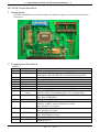
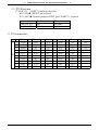
ELAN MICROELECTRONICS CORP.
ICE5840 User’s Guide
For
EM785840
EM785841
EM785842
EM78P5840
EM78P5841
EM78P5842
Version 2.1
2007/1/30
ELAN MICROELECTRONICS CORP.
No. 12, Innovation 1st RD., Science-Based Industrial Park
Hsin Chu City, Taiwan.
TEL: (03) 5639977
FAX: (03) 5780118
[ ELAN Communication line Development Reference \
ELAN In Circuit Emulator
1 Introduction
ICE5840 is intended to provide the product development engineer a powerful microcontroller
design tool.
2 Components description:
Table 1:
Symbol
U1
U2
Function
EM78R5840
27C256
Y1
S1
K1
JP1
JP2
JP3
JP6
Oscillator
Reset button
Option switch
ICE interface
ICE interface
Function pin
Program ROM
select
Program HOLD
JP8
JP9
JP11
JP12
JP13
R14
D1
Description
EM78R5840 Romless IC
8-bit data width DIP package memory (EPROM).
It mimicked to 4K word (8K bytes) embedded Program ROM.
32.768KHz crystal.
Reset from /Reset pin.
Refer to Table 3,4,5.
Connect to GIC board
Connect to GIC board
Connect to user application board, refer to Table6.
Connect to VDD : GIC mode, emulate with PC. Don’t connect U2
Connect to GND : External Rom mode, U2 as program Rom.
Open : developing program on ICE.
Short : Run on Piggyback.
P71/Reset
P71/Reset as reset pin or general reset.
P70/PLLC/ERCI P70/PLLC as PLLC connect capacitance to GND.
P70/PLLC as ERCI, connect resistance to VDD.
Open: P70/PLLC as I/O port.
XIN/P61
Short: Xin/P61 as Oscillator pin.
Open: Xin/P61 as I/O port.
XOUT/P60
Short: XOUT/P60 as Oscillator pin.
Open: XOUT/P60 as I/O port.
Resistance
Resistance for ERC
LED
Indicates Power.
W 1-2
X
[ ELAN Communication line Development Reference \
2.1 Power on the E8 ICE before executing the control software, or an error message
due to lack of hardware will appear.
2.2 E8 - ICE uses the printer cable to communicate with host PC. If a user wants to
use the Printer, it is recommended to install another printer port.
2.3 Printer port and the adapter locate on the right side. The ICE connects to
personal computer by printer port. The adapter connects to the power. Be sure
turn power off of ICE before plug in the adapter for avoiding over current which
may be burn the chip off.
2.4 Power on switch located on the same side as printer port. By switching to turn
off or turn on the ICE power.
2.5 On the top sight, we have some connections and one EM78R5840 Romless chip
and some switches. The JP1 and the JP2 connect to the second layer of ICE for
the code instruction accessing. The JP3 is more important for ICE user. They are
the EM78R5840 control signals and I/O ports. ICE user can connect these
connections to user's application board. The connections are list in Table1.
2.6 The U1 is EM78R5840 Romless chip. The U2 is a 4K words ROM for on board
testing by piggyback. If user has developed application code by this ICE. User
can use PIGGYBACK (user can buy from ELAN) to connect to user's
application board with 4K word EPROM (27c128 ~ 27C512). To verify user's
program.
2.7 The D1 is a LED that indicates power is on or off.
2.8 Run WICE software to enter ICE environment.
2.9 User can use file “*.MIX” which generate by WICE for masking EPROM .
The *.mix file is a binary file and addressing from zero.
2.10 For different voltage system, user can select 5.0V or 3.6V.
The bottom layer of ICE (called GIC layer), JP1 selction:
Open : 3.6V
Short : 5.0V
Here
W 1-3
X
[ ELAN Communication line Development Reference \
3 Setting
3.1 ICE and Piggyback
Table 2:
U2
No
JP1,JP2
JP4,JP5
JP6
JP7
JP8
ICE
Connect to VDD (upward) VDD (upward)
Open Open
GIC board
Piggyback EPROM No
VDD (upward) GND (downward) Open Short
3.2 K1 define:
Table 3:
1
2
3
AIR3 AIR2 AIR1
4
AIR0
5
P71S
6
P70S
7
8
9
10
OSCM1 OSCM0 IRC2S TEST
3.3 Crystal, ERC, IRC mode
Table 4:
Mode
Crystal
mode
ERC mode
IRC mode
K1
P70 used
PLL used
6
7
8
10
ON
OFF OFF OFF
OFF
NA ON OFF OFF
NA ON ON OFF
JP11
Open
Leftward
Rightward
Open
JP12 JP13
P60 P61
Short Short
Open Open
Open Open
3.4 IRC frequency
3.4.1 IRC2S: Internal RC oscillating frequency (for system CLK) select.
Connect to GND Î 2M Hz
Connect to VDD Î 4M Hz
3.4.2 AIR0~AIR3: Oscillating frequency adjustor.
Table 5:
AIR3 ~ AIR0
0000
0001
0010
0011
0100
0101
0110
0111
1000
1001
1010
1011
1100
1101
1110
1111
Frequency
1.05*F
1.10*F
1.15*F
1.20*F
1.25*F
1.30*F
1.35*F
1.40*F
0.65*F
0.70*F
0.75*F
0.80*F
0.85*F
0.90*F
0.95*F
1.0*F
* ”F” means the frequency of IRC output.
W 1-4
X
[ ELAN Communication line Development Reference \
3.5 P71/Reset pin
P71S (K1.5) : PORT71 function select bit:
K1.5 ON Î /RESET pin selected.
K1.5 OFF Î General purpose INPUT port “PORT71” selected.
K1.5
Port71 as I/O
OFF
Port71 as /Reset ON
JP9
Leftward
Rightward
4 I/O connection
pin Name pin Name pin Name pin
1 VDD 11
P64
21 P76 31
2 GND 12
P65
22 NC 32
3 /Reset 13
NC
23 NC 33
4 GND 14
NC
24 NC 34
5
VCC 15
P70
25 NC 35
JP3
6
VCC 16
P71
26 NC 36
7
P60
17
NC
27 NC 37
8
P61
18
P73
28 NC 38
9
P62
19
P74
29 NC 39
10
P63
20
P75
30 NC 40
W 1-5
X
name
P90
P91
P92
P93
P94
P95
P96
P97
NC
NC
pin Name pin
41 NC 51
42 NC 52
43 NC 53
44 NC 54
45 NC
46 NC
47 NC
48 PC1
49 PC2
50 NC
Name
NC
NC
NC
NC