1
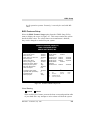
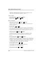
MGPS-PNTM System Board
User's Guide
P/N: 771946
Version: D01
April 1995
Mylex MGPS-PNTM System Board
Manual Notice
The information contained herein is subject to change without notice. Mylex does not
represent or warrant that this Installation and Operations Guide is correct in any or all
respects, and shall not be liable for technical or editorial omissions or errors made herein.
Except as specifically provided herein, Mylex makes no warranties, express or implied,
respecting this guide or the Mylex products referred to herein, including but not limited
to any warranty of design, merchantability, or fitness for a particular purpose, even if
Mylex has been informed of such purpose.
P/N: 771946
Version: D01
© Copyright 1995 by Mylex Corporation
P.O. Box 5035
Fremont, California 94537-5035
Copyright Notice:
This manual is copyrighted by Mylex Corporation. It may not, in whole or in part, be
copied, reproduced, photocopied, translated on paper, electronic media or computerreadable-form or be used to make a derivative work without written permission from
Mylex Corporation, except as permitted by the United States Copyright Act of 1976, as
amended.
FCC Warning:
This device has been tested and found to comply within the limits of a class B device,
pursuant to Part 15 of FCC regulations. Operation is subject to the following two
conditions:
1)
This device may not cause harmful interference.
2) This device must accept any interference received, including interference that may
cause undesired operation.
This equipment has been designed to provide reasonable protection against harmful
interference in a residential area. This equipment generates, uses, and can radiate radio
frequency energy. This device, if not installed and used in accordance with the
manufacturer's instructions, may cause harmful interference to radio communications.
There is no guarantee, however, interference will not occur in a particular installation.
Should it be determined that this equipment is causing interference to radio or television
reception, the following suggestion actions may be taken.
Reorient or relocate the receiving antennae. Increase the distance between the antennae
and the computer. Plug the computer into a different AC outlet so that the two conflicting
devices are using a different branch circuit. Contact the dealer who sold this equipment
and/or a reputable radio/television service technician for additional suggestions.
Only equipment certified to comply with Class B (computer input/output devices,
terminals, printers, etc.) should be attached to this equipment, and must have shielded
interface cables.
Finally, any changes or modifications to the equipment by the user not expressly
approved by the guarantee or manufacturer could void the users's authority to operate
such equipment. Trademarks: Mylex and MGPS-PNTM are registered trademarks of
Mylex Corporation. All other products and companies are trademarks of their respective
owners and licensees.
Manual No. 771946-D01, Apr. 1995
i
Mylex MGPS-PNTM System Board
Mylex Warranty
This product is guaranteed to be free from manufacturing or material defects for a period
of 1 (one) year after the date of purchase. Should the product fail during this period,
Mylex will repair or replace (at Mylex's option) the product free of charge with the
following provisions:
1)
Proof of purchase must be provided.
2) The product must have been properly installed in accordance to the documentation
provided.
3) The product must not have been modified by any party except by Mylex or an
authorized agent.
4)
The product must be free of damage.
Any software, including firmware, is provided “as-is” without warranty of any kind,
expressed or implied. The purchaser bears complete risk of the performance and quality
of the software. Mylex's sole responsibility, and the purchaser's only remedy to any
defect in workmanship, shall be replacement of the defective medium (diskette or ROM).
All expressed or implied warranties for the this product, including, but not limited to
warranties of merchantability and fitness for a particular purpose, are restricted to the
duration of the warranty period. Under no circumstances shall Mylex be held liable, in
any way, to the purchaser for damages, including any lost profits, lost savings, or other
incidental or consequential damages arising out of the use of, or inability to use this
product. Some states do not allow warranty or liability restrictions or limitations, so the
preceding limitations may not apply to you.
ii
Manual No. 771946-D01, Apr. 1995
Customer Service Policy
Returned Merchandise Authorization (RMA)
All products returned to Mylex for warranty service or for other reasons must be assigned
an RMA number before shipment to Mylex. The RMA number may be obtained by
contacting Mylex's Technical Support Department. Any product received without an
RMA number will be returned to the shipper unopened.
Important Note: Only the company (or individual) that purchased the product directly
from Mylex may obtain an RMA number. If the Mylex product was purchased from a
reseller or distributor, you must contact that company for service.
The following rules/procedures apply to all RMAs:
1)
The product must be returned in original packaging or other suitable materials.
2) Each returned unit will be inspected for damage or other irregularities. It a unit is
shown to be modified, the customer will be notified before any action is taken.
3) Mylex will not be responsible for non-Mylex products shipped with an RMA unit.
This includes memory, math co-processors and other internal and external peripherals.
Products must be shipped to Mylex with freight paid. Upon completion of service, Mylex
will ship the product back UPS Ground or similar service, at no charge, unless prior
arrangements have been made.
Customer Service
End users are required to contact their suppliers.
Mylex Technical Support is available 8:00 a.m. to 5:00 p.m. Pacific Standard Time,
Monday through Friday except holidays. Contact Mylex Technical Support by voice at
(510) 796-6100 or by fax at (510) 745-7715. You can also contact Technical Support
through their e-mail service at [email protected].
Manual No. 771946-D01, Apr. 1995
iii
Mylex MGPS-PNTM System Board
Handling Precautions
This product contains electronic components that are highly sensitive to electrostatic
discharge. Use extra caution when handling this product to ensure there is adequate
grounding around the work area the board is being installed. ALWAYS wear a ground
strap or ground your body by touching a grounded object such as an unpainted metal
device connected to power ground.
This product has delicate crystal oscillators that can break if subjected to sudden shock
such as being tossed on a table. Use care when moving it from point to point.
If Troubles Are Encountered
If this product displays improper operation during the course of installation or operation,
make sure that all components are seated tightly and configured correctly. Pay particular
attention to the jumper settings and the BIOS setup. If the product continues to operate
improperly, contact your dealer or distributor for additional information.
Dealers and Distributors may contact Mylex's Technical Support Department at (510)
796-6100 after first completing the enclosed System Problem Report.
Package Contents
MGPS-PNTM System Board
This User's Guide
Warranty Card
Any pertinent release notes available at the time of shipment
System Problem Report Form
Utility Diskette
iv
Manual No. 771946-D01, Apr. 1995
Contents
1 – Introduction
About This User's Guide .
1-1
The Green PC Function . .
1-2
Specifications . . . . . . . . . .
1-3
Jumpers and Connectors. .
1-4
.....................................
.....................................
.....................................
.....................................
2 – System Board Setup
Installing the CPU . . . . . . . . . . . . . . . .
2-1
System Board Jumpers . . . . . . . . . . . . .
2-2
System Clock Speed (JP10, JP11) .
2-3
Cache SRAM Voltage (JP28) . . . .
2-3
Flash ROM BIOS (JP30). . . . . . . .
2-4
System Board Connectors. . . . . . . . . . .
2-5
Keyboard (J1) . . . . . . . . . . . . . . . .
2-6
Power Supply (J2) . . . . . . . . . . . . .
2-6
RS-232-2 (COM2) Serial Port (J3)
2-7
RS-232-1 (COM1) Serial Port (J4)
2-7
Parallel Printer Port (J5) . . . . . . . .
2-7
Manual No. 771946-D01, Apr. 1995
...........................
...........................
...........................
...........................
...........................
...........................
...........................
...........................
...........................
...........................
...........................
v
Mylex MGPS-PNTM System Board
Floppy Drive Controller (J6) . . . . . . . . . . . . . . . . . . .
2-7
Hard Disk Drive IDE Controller (J7) . . . . . . . . . . . .
2-7
Power Management Mode Control (JP2) . . . . . . . . . .
2-7
HDD Activity Indicator (JP12) . . . . . . . . . . . . . . . . .
2-8
Keyboard Lock Switch and Power-On LED (JP22) . .
2-8
Turbo LED (JP23) . . . . . . . . . . . . . . . . . . . . . . . . . . .
2-8
System Reset Switch (JP24) . . . . . . . . . . . . . . . . . . .
2-9
Turbo Switch (JP25) . . . . . . . . . . . . . . . . . . . . . . . . .
2-9
External Speaker (JP26) . . . . . . . . . . . . . . . . . . . . . .
2-9
Jumpers & Connectors Quick Reference . . . . . . . . . . . . .
2-11
.............
.............
.............
.............
.............
.............
.............
.............
.............
.............
3 – Memory Installation
Main Memory . . . . . . . . . . . . . . . . . . . . . . . . . . . . . . . . . . . . . . . . . . . . . . .
3-1
Main Memory Configurations . . . . . . . . . . . . . . . . . . . . . . . . . . . . . . .
3-2
External Cache Memory . . . . . . . . . . . . . . . . . . . . . . . . . . . . . . . . . . . . . . .
3-3
vi
Manual No. 771946-D01, Apr. 1995
4 – BIOS Setup
CMOS Setup Utility . . . . . . . . . . .
4-1
Standard CMOS Setup . . . . .
4-2
BIOS Features Setup . . . . . . .
4-3
Virus Warning . . . . . . . .
4-3
Cache Control . . . . . . . .
4-4
Boot Up Features . . . . . .
4-4
IDE HDD Block Mode: .
4-5
Typematic Rate Setting .
4-5
Security Option . . . . . . .
4-5
System BIOS Shadow . .
4-6
Chipset Features Setup . . . . .
4-7
Power Management Setup . . .
4-8
Power Management Timers . .
4-9
Disable Mode. . . . . . . . .
4-9
Max. Saving Mode. . . . .
4-9
Min. Saving Mode . . . . .
4-9
User Define . . . . . . . . . .
4-9
Power Management Events . .
4-11
PM Control by APM . . .
4-11
Video Off Option . . . . . .
4-11
Manual No. 771946-D01, Apr. 1995
...............................
...............................
...............................
...............................
...............................
...............................
...............................
...............................
...............................
...............................
...............................
...............................
...............................
...............................
...............................
...............................
...............................
...............................
...............................
...............................
vii
Mylex MGPS-PNTM System Board
Video Off method . . . . . . .
4-12
Suspend Switch . . . . . . . . .
4-12
Doze Speed (div by): 2 . . .
4-12
Standby Speed (div by): 3 .
4-12
PCI & Onboard I/O Setup . . . . .
4-13
PCI IRQ Activated By . . . .
4-14
PCI IDE IRQ Map To . . . .
4-14
Load Setup Defaults . . . . . . . . .
4-15
Password Setting . . . . . . . . . . . .
4-15
IDE Hard Disk Auto Detection .
4-16
Hard Disk Low Level Format . .
4-17
Save and Exit Setup . . . . . . . . .
4-17
Exit Without Saving . . . . . . . . .
4-17
.............................
.............................
.............................
.............................
.............................
.............................
.............................
.............................
.............................
.............................
.............................
.............................
.............................
A – Updating the System BIOS
viii
Manual No. 771946-D01, Apr. 1995
Chapter 1
Introduction
About This User's Guide
This manual is arranged to help you set up and run the MGPS-PNTM
system board.
• Chapter 1, Introduction, describes the functions and features of the
system board and specifications.
• Chapter 2, System Board Setup, includes detailed information on
how to install and configure the MGPS system board.
• Chapter 3, Memory Installation, describes the size and
configuration of the on-board memory and external cache memory,
and gives instructions for installing the memory devices on the
system board.
• Chapter 4, BIOS Setup, explains how to adjust the BIOS setup
using the software to make use of the board's multiple features.
• Appendix A, Upgrading the BIOS, gives instructions on how to
update the BIOS Flash ROM using the manufacturer's latest
software.
Manual No. 771946-D01, Apr. 1995
1-1
Mylex MGPS-PNTM System Board
The Green PC Function
The Power Management Unit (PMU) controls and dramatically reduces
overall system power consumption. This is accomplished by the activity
monitors, which detect the system inactivity timer time-out, and signals
the power-saving devices to slow down the clock frequency or remove
the power sources from various peripherals.
There are four power management modes: Normal, Doze, Standby, and
Suspend.
• NORMAL mode: This mode is the normal operation of the PC
system. In this mode, the doze timer starts counting if no activity
is taking place and the programmable time-out period has expired.
• DOZE mode: In this mode, the CPU clock frequency is slowed to
one-half the normal frequency.
• STANDBY mode: This mode scales the CPU and system clock to
a lower frequency (8MHz) and turns off the video signal to
conserve power to the display monitor.
• SUSPEND mode: In this mode, the PMU stops the CPU clock,
slows down the system clock, and powers down the external cache.
The power management setup is described under BIOS Setup in
Chapter 4.
1-2
Manual No. 771946-D01, Apr. 1995
Introduction
Specifications
CPU Types
Supported:
System Clock:
Memory:
Intel Pentium™ Processor 75/90/100 MHz (P54C)
CPU ZIF socket 5 installed
50/60/66 MHz
Four 72-pin (32- or 36-bit) SIMM sockets, 1, 2, 4, 8, 16,
or 32MB SIMM's, 70ns or faster
Maximum 128MB on-board system memory
Cache Memory: Supports 256KB, 512KB, or 1MB;
32Kx8, 64Kx8, 128Kx8 DIP standard and 3.3V or mixed
voltage (5V supply, 3.3V output) SRAM
Maximum cache is 1MB
On-Board I/O
Expansion Slots:
Two RS-232-C serial outputs (COM1 and COM2), one
parallel printer port, floppy disk drive controller, and IDE
hard disk drive controller.
ISA bus 16-bit x 5
PCI Local Bus x 3 (all are master mode)
Shadow RAM:
BIOS:
PCB Size:
Turbo Speed:
Green PC:
System BIOS, video BIOS and adapter ROM BIOS
Award Pentium™ PCI BIOS with NCR PCI SCSI BIOS
220 x 330 mm 4-layer PCB
Software/hardware toggle controlled
Meets EPA Green PC standard. Power consumption is
under 30W during the Doze, Standby or Suspend mode
Manual No. 771946-D01, Apr. 1995
1-3
Mylex MGPS-PNTM System Board
Jumpers and Connectors
The following is a list of the jumpers and connectors used on the MGPSPNTM system board. The referenced pages provide more details.
Jumper / Connector No.
Function
Ref Page
J1
Keyboard Connector
2-6
J2
Power Supply Connector
2-6
J3
RS-232-2 (COM2) Connector
2-7
J4
RS-232-1 (COM1) Connector
2-7
J5
Parallel Printer Connector
2-7
J6
Floppy Drive Connector
2-7
J7
IDE HDD Connector
2-7
JP1
SIMM Module Setting Jumper
2-1
JP2
Power Saving Toggle Switch Connector
2-7
JP7, JP8
Cache Size Setting Jumper
2-3
JP10, JP11
System Clock Setting Jumper
2-3
JP12
HDD Activity LED Connector
2-8
JP21
Reserved (Open)
NA
JP22
Keyboard Lock Connector
2-8
JP23
Turbo LED Connector
2-8
JP24
Reset Switch Connector
2-9
JP25
Turbo Switch Connector
2-9
JP26
Speaker Connector
2-9
JP28
Cache SRAM Voltage Setting Jumpers (2)
2-3
JP30
Flash ROM Setting Jumper
2-4
1-4
Manual No. 771946-D01, Apr. 1995
Chapter 2
System Board Setup
This chapter describes the individual jumpers and connectors switches on
the MGPS-PNTM system board. If your system board has already been
installed by the dealer, you should refer to this chapter if you plan to
make any changes or upgrade your system.
Installing the CPU
The Intel Zero Insertion Force (ZIF) socket incorporated on the MGPS
system board is designed specifically for the Pentium processor. When
inserting the Pentium onto the socket, make sure pin 1is properly aligned
with the angled corner of the socket. Figure 2-1 illustrates the alignment.
Figure 2-1. Pentium CPU Pin Alignment
Locate the dot and notch Pin 1) on one of the processor's corners and the
angled corner of the ZIF socket. Raise the ZIF socket arm and insert the
processor into the socket with pin 1 aligned at the angled corner. Fully
lower the socket arm to lock the processor in place.
Manual No. 771946-D01, Apr. 1995
2-1
Mylex MGPS-PNTM System Board
System Board Jumpers
Jumpers are used to select between various operating modes or options.
A jumper switch consists of two or three gold pins projecting from the
system board. Placing the plastic jumper cap over two pins connects
those pins and makes a particular selection. If the cap is not placed over
two pins, the pins are open and a connection is not made. This is the
general method for storing jumpers when a connection is not required.
For all of the following jumpers,
• 1 – 2 indicates that a jumper is to be installed between pins 1 and
2 (pin 1 is identified only on connectors with 3 or more pins).
• 2 – 3 indicates that a jumper is to be installed between pins 2 and 3.
• “Short” indicates a jumper is installed on a connector with 2 or
more pins.
• “Open” or no entry indicates that no jumper is to be installed
(store the jumper on one pin only).
Figure 2-2 illustrates the jumper pins and cap, and the schematic
equivalent. The Jumpers and Connectors Quick Reference located at the
end of this chapter provides a layout of the system board to identify
major components, jumpers and connectors.
Figure 2-2. Jumper Pins, Cap and Layout
2-2
Manual No. 771946-D01, Apr. 1995
System Board Setup
The following jumpers are used on the MGPS-PNTM system board.
Please refer to the referenced pages for additional details:
Jumper No.
Function
Ref. Page
JP1
Main Memory SIMM type
3-1
JP7, JP8
Cache Memory Size
3-3
JP10, JP11
System Clock Speed
2-3
JP28
Cache SRAM Voltage
2-3
JP30
Flash ROM BIOS
2-3
System Clock Speed (JP10, JP11)
The MGPS system board supports Intel 75/90/100 MHz Pentium
processors (P54C), running at equivalent system clock speeds. You must
set the System Clock setting jumpers (JP10 and JP11) to match the speed
of the microprocessor.
Clock Setting Jumper
CPU Type
System Clock
JP10
JP11
P54C-75
50 MHz
Open
Open
P54C-90
60 MHz
Open
Short
P54C-100
66 MHz
Short
Short
Cache SRAM Voltage (JP28)
Cache SRAM's may be 3.3V or mixed voltages (5V supply, 3.3V output).
Insert two jumper caps to short the two pairs of Vcc3 pins for 3.3V
SRAM's; short the two pairs of Vcc pins when using 5V or mixed
voltage SRAM's (shown below set for Vcc = mixed voltage).
1
4
1
4
Vcc3 = 3.3V
(short 1-1 and 2-2)
Manual No. 771946-D01, Apr. 1995
JP28
Vcc = Mixed Voltage
(short 3-3 and 4-4)
2-3
Mylex MGPS-PNTM System Board
Flash ROM BIOS (JP30)
Set jumper JP30 (3-pins) for programming the flash ROM BIOS. Full
details with display menus to upgrade the system BIOS are presented in
Appendix A of this User's Guide. Please refer to Appendix A for
instructions on how to upgrade your system BIOS.
JP30
2-4
Description
1-2
Normal Operation (default)
2-3
System BIOS Programming mode
Manual No. 771946-D01, Apr. 1995
System Board Setup
System Board Connectors
Connectors interface the system board to other parts of the system,
including the power supply, drives, keyboard and various controls on the
front panel of the system case. Some connectors are polarized and
require specific alignment during installation. Polarized connectors are
shown with a plus (+) sign to denote the positive pin.
The following connectors are available on the MGPS system board:
Conn. No.
Function
Ref. Page
J1
Keyboard
2-6
J2
Power Supply
2-6
J3
RS-232-2 (COM2) Serial Port
2-7
J4
RS-232-1 (COM1) Serial Ports
2-7
J5
Parallel Printer Port
2-7
J6
Floppy Drive Controller
2-7
J7
IDE Hard Disk Drive
Controller
2-7
Power Saving Toggle Switch
2-7
JP12
HDD Activity LED
2-8
JP21
Reserved (Open)
JP22
Keyboard Lock/Power-On LED
2-8
JP23
Turbo LED
2-8
JP24
System Reset Switch
2-9
JP25
Turbo Switch
2-9
JP26
External Speaker
2-9
JP2
Manual No. 771946-D01, Apr. 1995
2-5
Mylex MGPS-PNTM System Board
Keyboard (J1)
This 5-pin DIN connector interfaces the keyboard to the system board.
J1-
Description
1
Keyboard Clock
2
Keyboard Data
3
No Connection
4
Ground
5
+5Vdc
Power Supply (J2)
Most power supplies have two 6-wire plugs that must be connected to the
system board. There are two black wires on each plug. Align the plugs
so that the two black wires on each plug are positioned in the middle of
the P1 connector as illustrated below. Before connecting to the power
supply, make sure it is not connected to the AC power source.
2-6
J2-
Description
Wire Color
1
Power Good
Orange
2
+5V
Red
3
+12V
Yellow
4
–12V
Blue
5
Ground
Black
6
Ground
Black
7
Ground
Black
8
Ground
Black
9
–5V
White
10
+5V
Red
11
+5V
Red
12
+5V
Red
Manual No. 771946-D01, Apr. 1995
System Board Setup
RS-232-2 (COM2) Serial Port (J3)
Use this I/O serial port to interface a variety of devices, such as a mouse,
modem, etc.
RS-232-1 (COM1) Serial Port (J4)
Use this I/O serial port to interface a variety of devices, such as a serial
mouse, modem, etc.
Parallel Printer Port (J5)
Interface a parallel printer to this port.
Floppy Drive Controller (J6)
A floppy disk drive controller adapter card is not required with the
MGPS system board. Connect a 5.25" or 3.5" floppy disk drive to this
on-board controller. Two floppy disk drives can be connected on a
standard drive cable in the same manner as when using a controller
adapter card.
IDE Hard Disk Drive Controller (J7)
A hard disk drive controller adapter card is not required with the MGPS
system board. Connect a hard disk drive to this on-board IDE controller.
Two hard disk drives can be connected on a standard drive cable in the
same manner as when using a controller adapter card.
Power Management Mode Control (JP2)
By connecting JP2 to a control switch on the front panel of the system
case, you can directly trigger the system into the Suspend mode. This
will reduce the CPU clock to zero MHz and power down the external
cache. The system can be resumed by again pressing the power saving
control switch or by using the auto-wake-up feature (pressing any key or
moving the mouse).
Manual No. 771946-D01, Apr. 1995
2-7
Mylex MGPS-PNTM System Board
The system will go into its power saving mode when the connector is
shorted by the mode control switch, and revert to normal operation when
the connector is open.
HDD Activity Indicator (JP12)
This 4-pin connector can interface an LED on the front panel of the
system case to indicate the activity status of the hard disk drive. The
connector has two sets of pins (1-2 and 3-4); either set may be used for
the respective LED (pins 1 and 4 are positive). Connect an LED between
pins 1 and 2, or pins 3 and 4 of JP12 to indicate the activity status of the
hard disk drive.
Keyboard Lock Switch and Power-On LED (JP22)
When connected to a key switch on the front panel of the system case,
turning and removing the key will disable the keyboard to prevent other
users from operating your computer when you are not present. Orient the
cable correctly when connecting the key switch to the main board; pin 1
is located on the top and pin 5 is on the bottom when viewing the board
as shown in the Quick Reference at the end of this chapter.
JP22-
Description
1
+5Vdc (Power-On LED)
2
No Connection
3
Ground (Power-On LED)
4
Keylock Switch
5
Ground
Turbo LED (JP23)
Install the turbo LED to this connector to indicate when the turbo
function is turned on. Observe polarity of the connector when installing
the LED.
2-8
Manual No. 771946-D01, Apr. 1995
System Board Setup
System Reset Switch (JP24)
This connector interfaces the system reset switch on the front panel of
the case. The switch causes the system board to perform a cold start
from the power-on self test without turning off power to components,
such as the hard disk drive.
JP24-
Description
1
System Reset
2
Ground
Turbo Switch (JP25)
A case-mounted toggle switch installed at this connector will permit you
to manually turn the turbo function on and off.
External Speaker (JP26)
An external speaker mounted inside the case can be interfaced to the
system board through this connector. Pin 1 is located on the bottom and
pin 4 is on the top when viewing the board as shown in the Quick
Reference at the end of this chapter.
JP26-
Description
1
Speaker Signal
2
Ground
3
Ground
4
+5Vdc
Manual No. 771946-D01, Apr. 1995
2-9
Mylex MGPS-PNTM System Board
2-10
Manual No. 771946-D01, Apr. 1995
Chapter 3
Memory Installation
The MGPS-PNTM system board provides SIMM installation slots for
2MB to 128MB of system memory. There is also an external cache
memory on the system board that can be installed with 0KB or up to
1MB in size. This chapter describes the types of memory devices that
should be used with the system board and explains how to install the
memory.
Main Memory
The system board supports any combination of 72-pin (32- or 36-bit)
SIMM's x 4 up to 128MB. The DRAM installation requires jumper JP1
to be set according to the use of single-side (S/S) or double-side (D/S)
SIMM's as illustrated in the table below. The on-board SIMM sockets are
illustrated in the Jumpers and Connectors Quick Reference fold-out page
at the end of Chapter 2. The socket pin arrangements are shown below.
Possible configurations are shown in the table on the next page.
BANK 0
SIMM 1
SIMM 2
S/S
D/S
72
S/S
D/S
1
BANK 1
SIMM 3
SIMM 4
—S/S
—S/S
—D/S
D/S
—D/S
D/S
JP1
1-2
2-3
Single-side 72-pin SIMM's are all 1MB, 4MB, or 16MB modules
SIMM 4
Double-side 72-pin SIMM's are all 2MB, 8MB, or 32MB modules
SIMM 3
—- = Empty
SIMM 2
SIMM 1
Manual No. 771946-D01, Apr. 1995
3-1
Mylex MGPS-PNTM System Board
Main Memory Configurations
No.
SIMM 1
BANK 0
SIMM 2
SIMM 3
BANK 1
SIMM 4
Total
Memory
1
1MB SS
1MB SS
——
——
2MB
2
1MB SS
1MB SS
1MB SS
1MB SS
4MB
3
2MB DS
2MB DS
4MB SS
4MB SS
12MB
4
2MB DS
2MB DS
——
——
4MB
5
2MB DS
2MB DS
2MB DS
2MB DS
8MB
6
2MB DS
2MB DS
8MB DS
8MB DS
20MB
7
2MB DS
2MB DS
16MB SS
16MB SS
36MB
8
4MB SS
4MB SS
——
——
8MB
9
4MB SS
4MB SS
4MB SS
4MB SS
16MB
10
8MB DS
8MB DS
4MB SS
4MB SS
24MB
11
4MB SS
4MB SS
16MB SS
16MB SS
40MB
12
8MB DS
8MB DS
——
——
16MB
13
8MB DS
8MB DS
8MB DS
8MB DS
32MB
14
8MB DS
8MB DS
16MB SS
16MB SS
48MB
15
8MB DS
8MB DS
32MB DS
32MB DS
80MB
16
16MB SS
16MB SS
——
——
32MB
17
16MB SS
16MB SS
16MB SS
16MB SS
64MB
18
32MB DS
32MB DS
16MB SS
16MB SS
96MB
19
32MB DS
32MB DS
——
——
64MB
20
32MB DS
32MB DS
32MB DS
32MB DS
128MB
3-2
Manual No. 771946-D01, Apr. 1995
Memory Installation
External Cache Memory
When you first install the cache memory on your system board or each
time you upgrade or modify it, you will need to adjust the cache memory
size setting for the appropriate memory level. The cache memory size for
the system is set with jumpers JP7 and JP87, as illustrated in the
following table.
Cache Size
Tag RAM
(U26-U27)
Data RAM
U26-U27
U35-U38
JP7
JP8
256K
8K x 8
32Kx8
32Kx8
1–2
1–2
512K
32K x 8
64Kx8
64Kx8
2–3
1–2
1MB (1024K)
32K x 8
128Kx8
128Kx8
2–3
2–3
Manual No. 771946-D01, Apr. 1995
3-3
Mylex MGPS-PNTM System Board
3-4
Manual No. 771946-D01, Apr. 1995
Chapter 4
BIOS Setup
Award's BIOS ROM has a setup program that allows you to modify your
basic system configuration. The BIOS data are stored in CMOS RAM so
that the setup configuration will be retained when the power is turned
off. Once the setup configuration is completed, you should need to
access the BIOS Setup program only when you plan to change the setup,
reset the date or time, etc.
CMOS Setup Utility
Power on the computer and press Del immediately to enter the Setup
program. The CMOS Setup Utility (Initial) menu is shown in Figure 4-1.
ROM PCI/ISA BIOS (2A51A000)
CMOS SETUP UTILITY
AWARD SOFTWARE, INC.
STANDARD CMOS SETUP
PASSWORD SETTING
BIOS FEATURES SETUP
IDE HDD AUTO DETECTION
CHIPSET FEATURES SETUP
HDD LOW LEVEL FORMAT
POWER MANAGEMENT SETUP
SAVE & EXIT SETUP
PCI & ONBOARD I/O SETUP
EXIT WITHOUT SAVING
LOAD SETUP DEFAULTS
ESC
Quit
↑↓→←
Select Item
F10
Save & Exit Setup
(Shift) F2
Change Color
Time, Date, Hard Disk Type
Figure 4-1. BIOS Setup Program Initial Menu
Manual No. 771946-D01, Apr. 1995
4-1
Mylex MGPS-PNTM System Board
Standard CMOS Setup
Choose the Standard CMOS Setup option from the CMOS Setup Utility
menu. The menu in Figure 4-2 allows you to configure date, time, hard
disk drive, floppy disk drive, display and memory. When a field is
highlighted, on-line help information is displayed in the left bottom of the
Menu screen. Cursor movement directions are at the bottom of the screen.
ROM PCI/ISA BIOS (2A5IA000)
STANDARD CMOS SETUP
AWARD SOFTWARE, INC.
Date (mm:dd:yy)
: Thu, Apr. 13 1995
Time (hh:mm:ss)
: 15:05:00
CYLS
HEADS
SECTOR
MODE
Drive C
: None (0Mb)
0
0
0
0
0
———
Drive D
: None (0Mb)
0
0
0
0
0
——
Drive A
: 1.44, 3.5 in
Drive B
: None
Drive A
: 1.44M
Drive B
: None
Video
Esc : Quit
: Modify
F1 : Help
LANDZONE
Base Memory
Extended Memory
Other Memory
Total
: EGA/VGA
Halt On
PRECOMP
640K
15360K
384K
16384K
: All Errors
↑↓→←
:
(Shift) F2:
Select Item
PU/PD/++/-
Change Color
Figure 4-2. Standard CMOS Setup Menu
Specifications for hard disk drives such as MFM, ESDI, or IDE, must be
recorded here. SCSI drives operate with device drivers and are not supported
directly by BIOS. The BIOS provides three modes to support IDE hard disks:
• Normal - for IDE drives smaller than 528MB, or as defined by
your controller or HDD specifications.
• LBA - for drives larger than 528MB and up to 8.4GB that use
Logic Block Addressing (LBA) mode.
• Large - for drives larger than 528MB that do not use LBA mode. The
Large mode is a new specification which may not be fully supported
4-2
Manual No. 771946-D01, Apr. 1995
BIOS Setup
by all operation systems. Presently, it can only be used with MSDOS.
BIOS Features Setup
Select the BIOS Features Setup option from the CMOS Setup Utility
menu to display the screen in Figure 4-3. This menu contains the system
board's default values. The values shown are manufacturer's defaults;
they can be changed as needed for your system.
ROM PCI/ISA BIOS (2A5IAC31)
BIOS FEATURES SETUP
AWARD SOFTWARE, INC.
Virus Warning
CPU Internal Cache
External Cache
Quick Power On Self Test
Boot Sequence
Swap Floppy Drive
Boot Up Floppy Seek
Boot Up NumLock Status
Boot Up System Speed
IDE HDD Block Mode
Gate A20 Option
:
:
:
:
:
:
:
:
:
:
:
Disabled
Enabled
Enabled
Disabled
A, C
Disabled
Enabled
On
High
Disabled
Fast
Typematic Rate Setting
Typematic Rate (Chars/Sec)
Typematic Delay
Security Option
:
:
:
:
Disabled
6
250
Setup
Video BIOS
C8000-CBFFF
Disabled
CC000-CFFFF
D0000-D3FFF
D4000-D7FFF
D8000-DBFFF
Disabled
DC000-DFFFF
Shadow
: Enabled
Shadow
:
Shadow
: Disabled
Shadow
: Disabled
Shadow
: Disabled
Shadow
:
Shadow
: Disabled
Esc
: Quit
↑↓→←
: Selection
F1
: Help
PU/PD/+/-
: Modify
F5
: Old Values
(Shift) F2
: Color
F6
: Load BIOS Defaults
F7
: Load Setup Defaults
Figure 4-3. Standard CMOS Setup Screen
Virus Warning
Disabled
Enabled
When enabled, this feature protects the boot sector and partition table
of your hard disk. Any attempt to write to them will halt the system
Manual No. 771946-D01, Apr. 1995
4-3
Mylex MGPS-PNTM System Board
and cause a warning message to appear. If this happens, you can
either allow the operation to continue or stop it.
Cache Control
CPU Internal Cache:
Disabled
Enabled
External Cache:
Disabled
Enabled
Boot Up Features
Quick Power On Self Test:
Disabled
Enabled
Allows the POST (Power On Self Test) procedure to run at either
normal or fast speed.
Boot Sequence:
A,C
C,A
This selects the drive for the system to search first for boot data. If
your system boots from the hard disk, you should select to search it
first and eliminate the time spent searching for the data in drive A.
Swap Floppy Drive:
Disabled
Enabled
Enabling this feature swaps the floppy drive assignment so that
drive A will function as drive B, and drive B will function as
drive A.
Boot Up Floppy Seek:
Enabled
Disabled
During POST Procedure, the BIOS will determine if the installed floppy
disk drive is 40 or 80 tracks (360KB is 40 tracks; 760KB, 1.2MB and
1.44MB are all 80 tracks). If this function is enabled, there will be a
warning message when a 360K floppy drive is installed.
Boot Up NumLock Status:
On
Off
ON: Keypad is set to number-mode keys following.
Off: Keypad is set to arrow-mode Keys.
Boot Up System Speed:
4-4
High
Low
Manual No. 771946-D01, Apr. 1995
BIOS Setup
If set to high speed, the system will run at high speed immediately
after power on.
IDE HDD Block Mode:
Disabled
Enabled
This feature enhances hard disk performance by making multisector
transfers instead of one sector per transfer. Most IDE drives, except
very early designs, can use this feature.
Gate A20 Option
Fast
Slow
Gate A20 controls the ability to access memory addresses above
1MB. It speeds up programs that constantly change from addressing
conventional memory to addressing memory above 1MB (between
real and protected address modes). For example, setting this option to
fast makes programs such as network operating systems execute
faster.
Typematic Rate Setting
Disabled
Enabled
This feature defines the keyboard's Typematic Rate and Typematic
Delay. When disabled, the default values of 6 characters/sec and
250ms delay are used.
Typematic Rate (Chars/Sec): The values are 6, 8, 10, 12, 15, 20, 24,
and 30 characters per second.
Typematic Delay (key repeat rate): The values are 250, 500, 750, and
1000 milliseconds
Manual No. 771946-D01, Apr. 1995
4-5
Mylex MGPS-PNTM System Board
Security Option
System:
Setup
System
Setup: The system will boot but access to the BIOS setup will be
denied until the correct password is entered.
System: The system will not boot and access to the BIOS setup will
be denied until the correct password is entered.
When either selection is enabled, a prompt will display for you to
enter and confirm your own password. If a password is totally lost,
you will need to reinstall the operating system in order to circumvent
the password requirement.
System BIOS Shadow
Enables the system shadow to achieve the best performance of the
system.
Video BIOS Shadow:
C8000-CBFFF:
CC000-CFFFF:
D0000-D3FFF:
D4000-D7FFF:
D8000-DBFFF:
DC000-DFFFF:
Disabled
Disabled
Disabled
Disabled
Disabled
Disabled
Disabled
Enabled
Enabled
Enabled
Enabled
Enabled
Enabled
Enabled
If you shadow the BIOS at any of the above segments, you can set
the appropriate memory cacheable function to Enabled
4-6
Manual No. 771946-D01, Apr. 1995
BIOS Setup
Chipset Features Setup
Choose Chipset Features Setup from the CMOS Setup Utility menu to
display the screen in Figure 4-4. This sample screen contains the
manufacturer's default values for the system board.
ROM PCI/ISA BIOS (2A5IAC31)
CHIPSET FEATURES SETUP
AWARD SOFTWARE, INC.
Auto Configuration
PCI Clock Frequency
ISA Bus Clock Frequency
CPU/PCI Burst Mem. Write
Disabled
CPU/PCI Post Mem. Write
: Enabled
: CPUCLK2
: PCICLK4
:
System BIOS Cacheable
Video BIOS Cacheable
Non-Cacheable Block 1
Block 1 Start Address
Block 1 Size
:
:
:
:
:
Disabled
Disabled
Disabled
0500000H
64KB
: Disabled
Esc
: Quit
↑↓→←)
: Select Item
F1
: Help
PU/PD/+/-
: Modify
F5
: Old Values
(Shift) F2
: Color
F6
: Load BIOS Defaults
F7
: Load Setup Defaults
Figure 4-4. Chipset Features Setup Menu
By enabling Auto Configuration, the BIOS will automatically detect the
CPU speed and auto-configure the bus frequency, DRAM speed, cache
and read/write cycle.
All the entries shown in this menu are optional settings for the system
board's chipset; the entries should not be changed.
Manual No. 771946-D01, Apr. 1995
4-7
Mylex MGPS-PNTM System Board
Power Management Setup
Choose Power Management Setup from the CMOS Setup Utility menu
to display the screen in Figure 4-5. This menu provides the Green PC
power management features.
ROM PCI/ISA BIOS (2A5IAC31)
POWER MANAGEMENT SETUP
AWARD SOFTWARE, INC.
Power Management
PM Control by APM
Video Off Option
Video Off Method
SYNC+Blank
: User Define
: Yes
: Susp,Stby-> Off
: V/H
**PM Timers**
HDD Power Down
: 10 Min
Doze Mode
: 1 Min
Standby Mode
: 5 Min
Suspend Mode
: 10 Min
**PM Events**
COM Ports Activity
: Enable
LPT Ports Activity
: Enable
HDD Ports Activity
: Enable
PCI/ISA Master Act
: Enable
IRQ1-15 Activity
: Enable
VGA Activity
IRQ3 (COM2)
IRQ4 (COM1)
IRQ5 (LPT2)
IRQ6 (Floppy Disk)
IRQ7 (LPT1)
IRQ8 (RTC OS2)
IRQ9 (IRQ 2 Redir)
IRQ10 (Reserved)
IRQ11 Reserved
IRQ12 (PS/2 Mouse)
IRQ13 (Coprocessor)
IRQ14 (Hard Disk)
IRQ15 (Reserved)
:
:
:
:
:
:
:
:
:
:
:
:
:
:
Disable
Enable
Enable
Enable
Enable
Enable
Disable
Enable
Enable
Enable
Enable
Enable
Enable
Enable
Esc
: Quit
↑↓→←)
: Select Item
F1
: Help
PU/PD/+/-
: Modify
F5
: Old Values
(Shift) F2
: Color
F6
: Load BIOS Defaults
F7
: Load Setup Defaults
Figure 4-5. Power Management Setup Menu
4-8
Manual No. 771946-D01, Apr. 1995
BIOS Setup
Power Management Timers
The four Power Management timer modes are set by pressing the
directional arrow keys ( ↑↓→← ). The four modes are:
• Disable
• Max. Saving
• Min. Saving
• User Define
Disable Mode
This mode disables the power management function; the system will be
in the non-green operation mode.
Max. Saving Mode
When you select this mode, you will be presented the system default
values of four related timers (HDD power Down Timer at 10 Min;
system Doze Timer at 20 Sec;, system Standby Timer at 20 Sec, and
system Suspend Timer at 20 Sec) to facilitate the minimized power
management function.
Min. Saving Mode
When you select this mode, you will be presented the system default
values of four related timers (HDD power Down Timer at 10 Min;
system Doze Timer at 40 Min; system Standby Timer at 40 Min; and
system Suspend at 40 Min) to facilitate the minimized power
management function.
User Define
You can define your own required power management delay values by
setting up the following four PM timers:
a. HDD Power Down Timer
Manual No. 771946-D01, Apr. 1995
4-9
Mylex MGPS-PNTM System Board
The entry period of this flexible HDD Off timer is 1 to 15 minutes.
Once the system stops reading from or writing to the HDD, the
standby timer starts counting. If there is no activity and the defined
timeout period expires, the system will shut off the HDD power. The
HDD will not resume its function until a read/write command is
executed.
b. Doze Timer
The Doze Timer starts counting at the end of each activity, If there is
no further activity during the defined period, the timer will scale the
CPU and system clock at the lower frequency (8MHz), and motivate
the enabled PM Events. When you press any keyboard key or move
the mouse, the CPU and system clock will auto-wake-up to a normal
operation.
The range of this standby mode timer is 10 seconds to 3 hours.
c. System Standby Timer
The Suspend timer starts counting at the end of each activity. If
there's no further activity during the defined period, the system will
scale the CPU and system clock at the lower frequency (8MHz) and
motivate the enabled PM Events. It will enable the monitor to enter
an inactive mode with a blank screen. The monitor will not display
again until you press any key or move the mouse.
The range of the Suspend mode timer is 10 seconds to 3 hours.
d. System Suspend Timer
The Suspend timer will be functional only if your system uses the
Intel SL-Enhanced series CPU. The Suspend timer starts counting at
the end of each activity. If there's no further activity during the
defined period, the system will shut off the CPU, HDD, and monitor
power to enter the Suspend mode.The power consumption in this
mode is even lower than that of the Standby mode.
The range of the Suspend mode timer is 10 seconds to 3 hours.
4-10
Manual No. 771946-D01, Apr. 1995
BIOS Setup
Power Management Events
Power Management Events include:
• Local Master
• Local Device
• Video Activities
• DMA Activities
• IRQ1 through IRQ15
The IRQ8 (RTC, OS2) default setting is disabled in order to make sure that
the Power Management mode can be executed under OS2. You can
customize a combination of PM Events by selecting “Enable”, which will be
checked whether or not the related function is still working before the
respective defined power management mode is asked to be motivated.
PM Control by APM
Yes
No
If APM (Advanced Power Management) is installed, the system
BIOS will wait for APM's prompt before entering any PM mode
(Doze, Standby, Suspend, User Defined).
Video Off Option
Always On
Suspend —> Off
Susp, Stby —> Off
All Modes —> Off
Always On: The system BIOS will never turn off the screen.
Suspend Off: Screen will turn off in the Suspend mode.
Susp, Stby Off: Screen will turn off in the Standby or Suspend
mode.
Manual No. 771946-D01, Apr. 1995
4-11
Mylex MGPS-PNTM System Board
Video Off method
Blank Screen
V/H SYNC+Blank
Blank: The system BIOS will blank the screen when disabling video.
V/H SYNC+Blank: The system BIOS will only blank the screen and
turn off the V/SYNC and H-SYNC signals from the VGA card to the
monitor.
A “Green” monitor detects the V/H SYNC signals to turn off its
electronic gun.
Suspend Switch
Enabled
Disabled
Pressing the power saving toggle switch connected to JP2 will cause
the screen to go into the Suspended mode immediately.
Doze Speed (div by): 2
During the Doze power saving mode, the CPU frequency will be
scaled to 1/2 of normal system frequency.
Standby Speed (div by): 3
During the Standby power saving mode, the CPU frequency will be
scaled to 1/3 of normal system frequency.
4-12
Manual No. 771946-D01, Apr. 1995
BIOS Setup
PCI & Onboard I/O Setup
This section provides information for configuring the PCI and Onboard
I/O features. Choose PCI & Onboard I/O Setup option from the CMOS
Setup Utility to display the menu shown in Figure 4-6.
Set all INT#'s to Auto. All PCI adapters should use INTA. The BIOS
will route each INTA to correspond to the IRQ automatically.
ROM PCI/ISA BIOS (2A5IAC31)
PCI & ONBOARD I/O SETUP
AWARD SOFTWARE, INC.
Slot 1 Using INT#
Slot 2 Using INT#
Slot 3 Using INT#
: AUTO
: AUTO
: AUTO
1st Available IRQ
2nd Available IRQ
3rd Available IRQ
4th Available IRQ
PCI IRQ Activated By
PCI IDE IRQ Map To
: 10
: 11
:9
: 12
: Edge
: ISA
Onboard FDC Controller
Onboard IDE Controller
Onboard Serial Port 1
Onboard Serial Port 2
COM3 & COM4 Address
Onboard Parallel Port
Parallel Port Mode
:
:
:
:
:
:
:
Enable
Primary
COM1
COM2
338H, 238H
278H
Normal
Esc
: Quit
↑↓→←)
: Select Item
F1
: Help
PU/PD/+/-
: Modify
F5
: Old Values
(Shift) F2
: Color
F6
: Load BIOS Defaults
F7
: Load Setup Defaults
Figure 4-6. PCI Configuration Setup Menu
Set all INT # to AUTO and all PCI adapters to use INTA. The BIOS will
automatically route each INTA to correspond with the IRQ.
The PCI Local Bus specifies four INTD (INTA-D) for each PCI slot. In
this board, INTA of slot 1, INTD of slot 2, and INTC of slot 3 will be
connected together and be directed to the first available IRQ. Also, the
2nd, 3rd, and 4th available IRQ's are also shared by the INT's of
different slots. Most PCI devices will use INTA as their interrupt pins,
and choose “AUTO” for the BIOS to automatically assign INT # to
different IRQ's. For PCI IDE adapter if you are using IRQ Paddle board,
set IRQ=NA. Otherwise, set IRQ=14 or 15.
Manual No. 771946-D01, Apr. 1995
4-13
Mylex MGPS-PNTM System Board
Slot 1
Slot 2
Slot 3
A
D
C
1st Available IRQ
B
A
D
2nd Available IRQ
C
B
A
3rd Available IRQ
D
C
B
4th Available IRQ
PCI IRQ Activated By
Level
Edge
To tell the chipset if the IRQ signals input is level or edge trigger.
Note: Most PCI controllers use LEVEL to activate the PCI IRQ.
PCI IDE IRQ Map To
PCI-AUTO
PCI-SLOT1
PCI-SLOT2
PCI-SLOT3
ISA
a. PCI AUTO
The BIOS will scan for PCI IDE devices to determine their
location and assign IRQ14 as the primary IDE INT #, and IRQ15
for the secondary IDE INT #.
b. PCI-SLOT#
Assign IRQ14 for the primary IDE INT # for the specified slot
number.
c. ISA
Some IDE cards connect the IRQ14 and IRQ15 directly from the
ISA slot through the card.
4-14
Manual No. 771946-D01, Apr. 1995
BIOS Setup
Load Setup Defaults
Select the Load Setup Defaults option from the CMOS Setup Utility
menu to configure the BIOS to load the system defaults directly from
CMOS. If the configured setup record created by the Setup program
becomes corrupted (and therefore unusable), the system defaults will be
loaded automatically when you turn the computer on. When you select
the option, you will be prompted to “Load Setup Defaults”. Respond
with Y or N as appropriate.
Password Setting
Select the Password Setting from the CMOS Setup Utility menu when
you want to initially set the password, and when you want to change or
delete an existing password. When you use this option to initially set a
password, you will be prompted to “Enter Password”. Press Enter (this
is the ROM default password) and continue to set up the initial
password. At other times, the prompt will require the valid password to
be entered.
After the ROM password (Enter) or valid password has been entered, you
can either accept the existing password, set up a new one, or delete the
password entirely. The password can be three to eight digits in length.
Remember that you may need to set the “Security Option” in the BIOS
Features menu to either “System” or “Setup” so that the password will
be required to run the system, or to access the BIOS setup only.
Manual No. 771946-D01, Apr. 1995
4-15
Mylex MGPS-PNTM System Board
IDE Hard Disk Auto Detection
This utility automatically detects the IDE hard disk type; use this to
confirm your hard disk data when it is unknown. Select the IDE HDD
Auto Detection from the CMOS Setup Utility menu. Upon detection, the
HDD type and peripheral data will be displayed. A prompt will display
in the center of the menu for you to accept or disregard the detected
drive.
ROM PCI/ISA BIOS (2A5IAC3)
STANDARD CMOS SETUP
AWARD SOFTWARE, INC.
CYLS
HEADS
PRECOMP
Drive C:
(124MB)
936
16
65535
Drive D:
( MB)
0
0
0
LANDZONE
SECTOR
935
17
0
0
MODE
Normal
——
Do you accept this drive D (Y/N)?
Select Drive D Option (N=Skip) : N
OPTIONS
SIZE
SECTORS
1(Y)
CYLS
HEADS
0
0
PRECOMP
LANDZONE
MODE
0
0
0
0
Normal
ESC : Skip
Figure 4-7. IDE HDD Auto Detection Menu
4-16
Manual No. 771946-D01, Apr. 1995
BIOS Setup
Hard Disk Low Level Format
This utility is the drive setup software used for low-level format before
DOS FDISK and FORMAT or similar utilities. You can use this utility
on MFM encoded hard disk drives if they require formatting but have not
been low-level formatted by the manufacturer. IDE, ESDI and SCSI
drives do not need this utility; you should not use it on these types of
drives.
CAUTION
All options in this utility are destructive to
data on a hard disk.
Save and Exit Setup
Select this option from the CMOS Setup Utility after you have
completed your BIOS setup and want to save all changes. Press Enter
after selecting the option and all changes will be written in the CMOS
memory of the chipset. The microprocessor will check this data
whenever you turn on your system, and compare it to what it finds in the
system.
Press Esc after selecting this option and you do not want to save & exit.
The initial screen will again display for you to select the option of your
choice.
Exit Without Saving
Select this option from the CMOS Setup Utility and press Enter to exit
the Setup program without saving any changes.
Manual No. 771946-D01, Apr. 1995
4-17
Mylex MGPS-PNTM System Board
4-18
Manual No. 771946-D01, Apr. 1995
Appendix A
Updating the System BIOS
This appendix provides instructions on how to update the system BIOS
using the FLASH ROM BIOS feature, which permits you to update the
BIOS without exchanging EPROM chips. Upon receipt of a
manufacturer's or dealer's diskette containing the BIOS update data,
perform the following to update the BIOS:
1. Turn off power to the computer and open the system case so you
can access jumper JP30.
2. Place a jumper cap on JP30 to short pins 1 and 2.
3. Turn on power to the computer.
4. Insert the BIOS data diskette in drive A or B. Make that drive
active and type “FLASH” at the DOS command line and press
Enter<. The following screen will be displayed.
FLASH MEMORY WRITER V1.2
Copyright (c) 1993, Award Software, Inc.
For SIS501 - 3A01A00
04/13/1995
Flash Type File Name to Program : 5slb1.bin
Error Message:
5. Type in the BIOS file name to program, which will be furnished
by your dealer when a new BIOS update is released. In the
screen above, the file name 5slb1.bin is shown already typed in.
As soon as you enter the file name and press Enter, a message
Manual No. 771946-D01, Apr. 1995
A-1
Mylex MGPS-PNTM System Board
will appear at the bottom of the screen to prompt if you want to save
the (current) BIOS data.
6. Press Y if you want to save the previous BIOS to the BIOS data
diskette. Press N if you do not want to save the previous BIOS
data.
7. Remove the jumper cap from JP30 pins 1 and 2 and place the
cap across pins 2 and 3 and press Enter. A prompt will display
the Error Message window to confirm that you want to proceed
with the update (“Are you sure to program (Y/N)”)
8. Press Y for Yes if you want to continue the BIOS update. Press
N for No if you want to quit without programming the BIOS
update. The following screen will display to show the status of
the update routine:
FLASH MEMORY WRITER V1.2
Copyright (C) 1993, Award Software, Inc.
For SIS501 - 3A01A00
04/13/1995
Flash Type - 28F010/12V
File Name to Program:
Blanking Flash Memory - 1FFFF OK
Erasing Flash Memory - 1FFFF OK
Programming Flash Memory - 1FFFF OK
Evaluation - Not For Sale
Warning : Don't Turn off Power or Reset System
9. Following successful update, the computer will auto-Restart.
10. Power down the computer.
10. Remove the JP30 jumper cap from pins 2 and 3 and place the
cap across pins 1 and 2 again. Power up the computer.
11. Enter the CMOS Setup and load setup defaults.
A-2
Manual No. 771946-D01, Apr. 1995
Jumpers and Connectors Quick Reference
I/O PORTS:
J7: Hard Disk Drive Connector
J6: Floppy Drive Connector
J5: Parrell Printer Port
J4: RS-232-1 (COM1) port
J3: RS-232-2 (COM2) Port
JP12: HDD Activity LED Connector
Main Memory Slots
J2: Power Supply Connector
J1: Keyboard Connector
JP28: Cache SRAM Voltage
JP1: Main Memory Configuration:
1-2: Bank0 and Bank1 are
installed at
the same time;
Bank0
is dedicated
in single-side SIMM's
2-3: Bank0 and Bank1 are
installed at
the same time;
Bank0 is dedicated
in double-side SIMM's
Vcc3 = 3.3V (2 jumpers)
Vcc = Mixed voltage, 5V
supply, 3.3V output
(2 jumpers)
Connectors:
JP2: Power Saving Green
Switch
JP21: Reserved
JP23: Turbo LED
JP26: External Speaker
JP25: Turbo Switch
Cache Size Selection (JP7, JP8)
JP7
256KB
512KB
1MB
1-2
2-3
2-3
System Clock Speed (JP10, JP11)
JP10
75MHz
90MHz
100MHz
Open
Open
Short
JP24: System Reset Switch
MGPS-PNTM System Board
PCB Revision