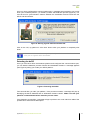
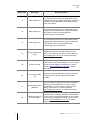
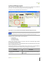
1
iBL
ingenia dsPIC
bootloader
Users’s guide
06/06/07
Version 1.4
© 2007, ingenia-cat S.L.
iBL User’s guide
Copyright and trademarks
Copyright © 2007 ingenia-cat, S.L.
Microchip, MPLAB and dsPIC are registered trademarks of Microchip Technology
Incorporated in the U.S.A. and other countries
Scope
This document applies to ingenia dsPIC bootloader.
Disclaimer
This product is provided “as is”. ingenia-cat expressly disclaims any warranty of any kind,
whether express or implied, including but not limited to, the implied warranties of
merchantability, fitness for a particular purpose, or non-infringement.
In no event shall ingenia-cat be liable for any incidental, special, indirect or consequential
damages, lost profits or lost data, harm to your equipment, cost of procurement of substitute
goods, technology or services, any claims by third parties (including but not limited to any
defense thereof), any claims for indemnity or contribution, or other similar costs.
User’s guide
iBL
Contents
Overview ............................................................................. 5
What is a bootloader? ............................................................ 5
ingenia dsPIC bootloader .......................................................... 6
Bootloader package .............................................................. 6
ingenia dsPIC bootloader firmware ............................................ 6
Requisites........................................................................ 6
How it works? ................................................................... 7
Communication Protocol Description ....................................... 8
How to use it with another dsPIC30F ...................................... 10
Limitations ..................................................................... 11
ingenia dsPIC bootloader Graphic User Interface .......................... 12
Requisites....................................................................... 12
Setting up the Hardware ..................................................... 12
Loading and Writing programs .............................................. 15
Running and reconnecting ................................................... 16
The XML dsPIC list file ........................................................ 16
Appendix A. ingenia bootloader Source Code ................................. 19
Appendix B. Example of dsPIC list file ......................................... 20
3
User’s guide
iBL
Icons
Following is shown the meaning of the icons that reader can find on this document.
Information
Provides the user with tips and tricks and other useful data.
Warning
Provides the user with important information. Omitting this warning may cause the
device not to work properly.
Critical Warning
Provides the user with critical information. Omitting this critical warning may
destroy the device.
4
User’s guide
iBL
1
Overview
This chapter introduces the bootloader strategy for MCUs.
What is a bootloader?
A serial bootloader is a firmware (software embedded in a hardware device) located into the
non-volatile memory of a microcontroller unit (MCU) that allows in-circuit reprogramming of
the device using its standard communication ports.
Usually, the process to program a MCU implies the need of an expensive hardware device.
Such devices, also called programmers, use the special purpose pins of the MCUs to access
to the internal memory. Modifying the voltage applied to these pins, a read or write cycle of
the memory could be performed.
Moreover, the programmers also should incorporate a serial interface in order to allow the
communications with the sender device (normally a Personal Computer (PC)). Together with
the hardware programmer, comes software that helps the final user to send his own firmware
through the serial port of the PC to the MCU.
In the other hand, a serial bootloader is just a piece of code that works with the
communication ports of an MCU and takes advantage of the capacity to write into his own
non-volatile memory.
This means that hardware programmer must be used at least once to load it into the MCU.
Then, the user can reprogram the MCU as many times as required without the need of the
hardware programmer.
One of the main advantages of using a serial bootloader in a hardware device that contains
a firmware, is that adds to it the capacity to be easily upgradeable (the user just needs a PC
to update the firmware version). This procedure will save the cost of disassemble and send
the device back to the factory.
Chapter 1: Overview
5
User’s guide
iBL
2
ingenia dsPIC bootloader
Description of the ingenia bootloader (firmware + GUI).
Bootloader package
ingenia has developed a serial bootloader package specially focused on the dsPIC30F
family of Microchip and tested with ingenia Communication Module (iCM4011).
Mainly the bootloader package is divided into two parts:
•
•
An open source firmware code (iBL) and,
A Windows based graphical user interface (GUI).
ingenia dsPIC bootloader firmware
As explained above, the firmware must be loaded into the MCU using a hardware
programmer.
ingenia offers iCM4011 development kit based on dsPIC30F which comes with
the bootloader already programmed inside. Contact ingenia for further
information.
The main features of ingenia’s bootloader firmware are:
•
•
•
•
•
Auto-Baud rate detection – The bootloader has the ability to adjust its own baud
rate to the one used by the sender by mean of a synchronization protocol.
Possibility of Read and Write Program (Flash) Memory – The bootloader is able
to access to the whole non-volatile memory dedicated to program code.
Possibility of Read and Write EEPROM Memory - The bootloader is able to
access to the whole non-volatile memory dedicated to data.
Possibility of Read and Write Configuration Registers - The bootloader is able to
access to the configuration registers zone.
Optimized assembler code – The firmware is implemented minimizing the used
code size.
Requisites
The system requirements to use ingenia bootloader package is shown in the Figure 1.
This system is composed by the following elements:
•
•
•
6
A personal computer with ingenia dsPIC bootloader Graphic User Interface installed.
A dsPIC30F Board with the firmware already loaded it and with a communications
transceiver (i.e. iCM4011).
The appropriate communication cable (USB, RS232, etc) according to the used
transceiver.
Chapter 2: ingenia dsPIC bootloader
User’s guide
iBL
Figure 1: Typical System
How it works?
Conceptually the firmware can be seen as a flow of states (see Figure 2). Below there is a
description of them and the conditions necessary to move from one to another.
•
•
•
•
•
•
•
Reset – When a power-up or a reset occurs the dsPIC enters in this state and
jumps directly to the Baud Rate Detection.
Baud rate detection – In this state, synchronization with the sender is performed
in order to compute the used baud rate. After a time (one second if 7.3728 MHz
crystal is used) if no synchronization is established a timeout occurs and the
execution goes to the User program. If the baud rate is detected correctly the
execution continues in the Wait Commands state.
Wait Commands – During this state the dsPIC listens continuously the UART
port. If a known command is received, the program will jump to the corresponding
state (version, read, write, or user program). Otherwise will stay in this state
indefinitely.
Version – The version of the Firmware is sent through the UART and the
execution returns to Wait Commands state.
Read – A read memory operation is realized, the result is sent through the UART
and the execution returns to Wait Commands state.
Write – A write memory operation is realized and the execution returns to Wait
Commands state.
User Program – The program execution jumps to starting user program address
(0x100) and therefore the bootloader ends.
Figure 2: Flow State Diagram of the bootloader
Appendix A: ingenia bootloader Source Code
7
User’s guide
iBL
Communication Protocol Description
As explained in How it works?, the firmware is composed by a set of states that can be
grouped into:
•
•
Baud rate detection or synchronization between the two devices.
Commands.
Following there is a detailed explanation of the functionality of each group.
Synchronization
In order to achieve a correct synchronization, the remote device should send continuously
the ASCII character ‘U’ (0x55) to the dsPIC. The representation of this character in binary is
01010101b giving the maximum frequency of transitions in a fixed baud rate (See Figure 3).
Figure 3: Representation of the character 0x55
When the bootloader detects the first rising edge, starts a timer and looks for the next four
rising edges. Once is detected the last edge one, the timer is stopped and the baud rate
computed by means of a simple division.
Commands
The frame of all the commands used by the bootloader starts with an Identification Byte. The
answer frame is always ended with acknowledge (ACK = 0x55) or non-acknowledge (NACK
= 0xFF) but the Reset command.
Firmware version command
Check the major and minor version of the firmware.
Command:
Answer:
Read command
Read the content of a position of the memory, which could be FLASH, EEPROM or
Configure registers addressed by a 24bits word. The answer is also a 24bits data word.
Command:
Answer:
8
Chapter 2: ingenia dsPIC bootloader
User’s guide
iBL
Write command
Carries out a write memory operation, which could be FLASH, EEPROM or Configure
registers.
The writing operation is done in row mode access (See Limitations for further information),
thus you should specify the initial address, the length of the row and the whole row content.
The frame ends with a CRC that is computed as the 256 module of all the data value
addition.
Command:
Answer:
or
User Program command
Force the user program execution, which should be located at address 0x100.
Command:
Answer: None
Unknown command
When an unknown command is received the bootloader sends a non-acknowledge.
Answer:
Appendix A: ingenia bootloader Source Code
9
User’s guide
iBL
RESET
no
BDR
received
from UART?
no
Timeout
yes
yes
Compute Baudrate
and configure UART
USER
CODE
dsPIC sends
ACK
yes
no
BYTE
received
from UART?
yes
Reset
command?
no
Version
command?
no
Read
command?
no
Write
command?
no
dsPIC sends
firmware version
Receive
address
Receive Frame
(address + N + data
+ CRC)
dsPIC sends
memory content
CRC OK?
no
dsPIC sends
NACK
Assigns Erase/Write Row
code and number of latches
depending on memory region
Erase Row (except if
Config register)
Load latches
dsPIC sends
ACK
Write Row
Figure 4: More detailed flowchart of the bootloader
How to use it with another dsPIC30F
The serial bootloader package comes with both, an MPLAB project and a compiled version
of the assembler file valid for the dsPIC30F4011.
However, if you want to use the firmware with another dsPIC30F family device you should
change the project and recompile it.
These are the steps to follow:
1.
2.
10
Start MPLAB and open the iBL.mcp project.
In the option Select Device of the menu Configure, select the device of your
system (see Figure 5).
Chapter 2: ingenia dsPIC bootloader
User’s guide
iBL
Figure 5: Selection of the device
3.
4.
In the project window remove the default linker script (p30f4011.gld) and add the
corresponding to your device (See Figure 6).
After that you should be able to recompile the project normally.
Figure 6: Modifying the linker script
Limitations
The bootloader firmware uses by default the alternate UART pins. If you want to use the
main UART pins you should replace the initialization as follows:
; Uart init
mov #0x8420, W0
; W0 = 0x8420 -> 1000 0100 0010 0000b
Appendix A: ingenia bootloader Source Code
11
User’s guide
iBL
mov W0, U1MODE
; Enable UART with Alternate IO, Auto Baud and 8N1
by
; Uart init
mov #0x8020, W0
mov W0, U1MODE
; W0 = 0x8020 -> 1000 0000 0010 0000b
; Enable UART with Main IO, Auto Baud and 8N1
The writing of the EEPROM and Flash memories uses only the row mode access.
Internally, the firmware erases and writes a whole row. Thus, to perform a correct writing
operation the sender must:
1. Ensure the initial address of writing match an initial row position.
2. Send the data corresponding to the whole row.
ingenia dsPIC bootloader Graphic User Interface
ingenia dsPIC bootloader Graphic User Interface allows loading a program into a dsPIC, by
using iBL (ingenia bootloader) firmware open source and an appropriate hardware platform
(such as iCM4011).
The following diagram shows this architecture:
Figure 7: Architecture for using ingenia dsPIC bootloader
Requisites
Minimum recommended system requirements for ingenia dsPIC bootloader Graphic User
Interface are:
9
9
9
CPU: Intel Pentium II (366 MHz or higher) with serial port for programming (USB
also available if using iCM4011)
Memory: 64 MB minimum
Operating System: Windows 2000/XP
Setting up the Hardware
Setting up the port and the baud rate
Before start the detection process of the dsPIC and bootloader firmware, you will have to
select the serial COM port where you will plug your dsPIC platform and the baud rate to use
for transferring data. The maximum allowed baud rate is 115200bps.
If you are working on a noisy electric environment or your serial cable is longer than five
meters, you may want to select a slower baud rate for transferring data.
12
Chapter 2: ingenia dsPIC bootloader
User’s guide
iBL
Once you have configured the communications port, a message pops up alerting you to shut
down your hardware platform (i.e. iCM4011) before start detection process (Figure 8). You
must do this for synchronization reasons between the bootloader firmware saved into the
dsPIC and this software.
Figure 8: Starting ingenia dsPIC bootloader GUI
Click on the ‘OK, my platform is shut down’ button when your platform is completely shut
down.
Check the ‘don’t remember me again’ option if you don’t want to be alerted next
time you run ingenia dsPIC bootloader.
Detecting the dsPIC
Once you have shut down the hardware platform and configured the communications port,
you can start the detection process of dsPIC and bootloader firmware. A message appears
(see Figure 9) asking you to start your dsPIC platform.
Figure 9: Detecting the dsPIC
Few seconds after you start your platform, if the process succeeds, a message will pop up
identifying the dsPIC detected and its bootloader firmware version. Make sure that your
platform is shutted down before detection process starts.
If the detection process fails, a message will pop up with an error code. Next is a table of the
possible error codes and its description:
Appendix A: ingenia bootloader Source Code
13
User’s guide
iBL
Error code
Error type
Error description
XML syntax error
An error has been found in your XML dsPIC list file
regarding the memory regions description. Verify that
you have correctly defined the three programming
zones of the dsPIC.
XML syntax error
An error has been found in your XML dsPIC list file
regarding the bootloader memory region description.
Verify that you have correctly defined this
programming zone of the dsPIC.
-3
XML syntax error
An error has been found in your XML dsPIC list file
regarding the protected memory regions description.
Verify that you have correctly defined these
programming zones of the dsPIC.
-4
Firmware detection
failed
ingenia's firmware has not been detected on the
device, or its version is not valid. Contact ingenia at
[email protected] for further information.
-1
-2
-5
dsPIC not found
-6
Error opening XML
file
Failed when opening XML dsPIC list file. Verify that
file exists and its name and path have not been
modified.
Wrong dsPIC zones
definition
One or more dsPIC memory zones are not properly
defined or its boundaries are not correct. Check
documentation on how to add a new device (see
Adding a new device) or contact ingenia at
[email protected] for further information.
Wrong protection of
memory regions
One or more protections of memory regions against
overwriting are not properly defined or its boundaries
are not correct. Check documentation on how to add
a new device (see Adding a new device) or contact
ingenia at [email protected] for further
information.
-7
-8
14
The dsPIC of the device has not been found on
dsPIC list file. Check documentation on how to add a
new device (see Adding a new device) or contact
ingenia at [email protected] for further
information.
Chapter 2: ingenia dsPIC bootloader
User’s guide
iBL
Loading and Writing programs
When you finish the detection process, you can load as many programs as you want into
your dsPIC. The loading & writing dialog window pops up (see Figure 10).
To load a file, click on the folder button and browse for it.
Click and
browse for
an HEX file
Writeable memory
zones of dsPIC
Figure 10: Loading & Writing Dialog
Supported file formats are Intel 16-bit and 32-bit hexadecimal object file format.
Intel's Hex-record format allows program or data files to be encoded in a printable
(ASCII) format. This allows viewing of the object file with standard tools and easy
file transfer from one computer to another, or between a host and target.
Writeable memory zones of a dsPIC can be divided into:
•
•
•
program flash
write data EEPROM
and configure registers
ingenia dsPIC bootloader shows you the three zones and its associated range address
accordingly with the detected dsPIC.
Once you load the HEX file, it will automatically detect the programmed zones and check
them in the appropriate check boxes.
ingenia dsPIC bootloader may detect possible overwrite conflicts when you load an HEX file.
The following table resumes the possible warning messages and its description.
Message
• code has data in bootloader
addresses
Appendix A: ingenia bootloader Source Code
Description
The HEX contains data in bootloader reserved
region. ingenia dsPIC bootloader will never write
on this zone.
15
User’s guide
iBL
• Your HEX file contains data in
protected 'code' addresses
• Your HEX file contains data in
protected ‘EPROM’ addresses
• Your HEX file contains data in
protected ‘config’ addresses
The HEX file contains data in protected regions.
You can omit the warning and continue the writing
process (the protected regions will not be
overwritten).
You can add protect regions of memory within a
writeable zone by editing the ibl_dspiclist.xml file
(see The XML dsPIC list file).
Once you have loaded the file you can start the write process by clicking on the ‘start write’
button.
Running and reconnecting
After loading (writing) a program into the dsPIC, you can run it either:
•
manually restarting your platform (hardware disconnection/reconnection)
•
clicking on the run button of ingenia dsPIC bootloader GUI.
or,
In the first option, the program will start after bootloader firmware times out waiting for
connection (see flowchart of Figure 4).
In the second option, a User Program command will be sent to bootloader firmware which
will force the user program execution. This option can only be used while keeping
synchronization between device and bootloader firmware.
After running the program, if you need to reconnect to the device you can click on the
reconnect button and restart your hardware platform.
COM and baud rates selected in the configuration process will be used.
The XML dsPIC list file
ingenia dsPIC bootloader can work with dsPIC30F family Digital Signal Controllers (for
instance iCM works with dsPIC30F4011). The detection process of dsPIC (see Detecting the
dsPIC) uses ibl_dspiclist.xml file to identify the controller and its features. This file is
located in the installation folder and consists in a list of supported dsPICs (or devices).
If the dsPIC that uses your platform doesn’t appear in that list, you can add them obeying the
XML syntax used in the file. Next section will help you to do that. A DTD enclosed with the
XML file will also help you check your XML syntax.
For further information on writing XML files refer to http://www.w3.org/XML/ .
A DTD ("Document Type Definition) is a set of declarations that conform to a
particular markup syntax and that describe a class, or "type", of SGML or XML
documents, in terms of constraints on the structure of those documents.
Adding a new device
Each dsPIC is named as a device in the XML dsPIC list file. A device is a description of a
dsPIC. They are characterized by an identifier, a name and the number of instruction rows
per page.
The identifier (id tag) is the Microchip device ID (DEVID).
The name (name tag) is the Microchip device name.
The number of rows per page (rowsxpage tag) is related to erase and program process of
dsPIC. In the dsPIC30F family must be always fixed to one.
Within tags <device></device> you have to define three memory zones:
16
Chapter 2: ingenia dsPIC bootloader
User’s guide
iBL
•
•
•
code or programming,
data,
and configuration
Code zone is represented with <memcode> tag.
Data zone is represented with <memdata> tag.
And configuration zone is represented with <memconfig> tag.
In each zone you need to define the start address, the end address and the number of
instruction per row as attributes of the tag.
Also within memcode zone you have to specify bootloader region by using <bootloader> tag.
The number if instructions per row are defined as follows:
• Code: 32 instructions per row
• Data: 16 instructions per row
• Config: 1 instruction per row
The bootloader region defines the zone where bootloader is located. This zone will be
protected against overwrites, so be sure to define its start and end address properly (you will
never be able to write code in this region).
The XML dsPIC list file comes with bootloader region defined for iCM. If you are
using a different platform, change it accordingly.
The following example shows a complete definition of a device.
<device id="0x0101" name="dsPIC30F4011" rowsxpage="1">
<memcode startaddress="0x000000" endaddress="0x007FFE"
instructionxrow="32">
<boot loader startaddress="0x007E00" endaddress="0x007FFE"/>
</memcode>
<memdata startaddress="0x7FFC00" endaddress="0x7FFFFE"
instructionxrow="16"/>
<memconfig startaddress="0xF80000" endaddress="0xF8000B"
instructionxrow="1">
</memconfig>
Protecting zones of your dsPIC
You can protect from overwriting memory regions of your dsPIC by using <protected> tag
within a memory zone.
To do that, specify the startaddress and the endaddress of the protected zone in the
attributes of <protected> tag.
<memconfig startaddress="0xF80000" endaddress="0xF8000B"
instructionxrow="1">
<protected startaddress="0xF8000A" endaddress="0xF8000B"/>
</memconfig>
The following example protects the memory region starting at 0xF8000A and ending at
0xF8000B in the configuration zone.
Appendix A: ingenia bootloader Source Code
17
User’s guide
iBL
You can protect as many regions as you want.
If you try to write code on those regions, ingenia dsPIC bootloader will alert you about that
and you will decide whether to proceed or not.
See section Appendix B for a complete example of an XML dsPIC list file.
18
Chapter 2: ingenia dsPIC bootloader
User’s guide
iBL
Appendix A. ingenia
Code
bootloader
Source
Last version of bootloader source code could be downloaded from ingenia-cat website
(www.ingenia-cat.com).
Appendix A: ingenia bootloader Source Code
19
User’s guide
iBL
Appendix B. Example of dsPIC list file
<?xml version="1.0" encoding="iso-8859-1"?>
<!DOCTYPE devices SYSTEM "ingeniadspicbootloader.dtd">
<devices>
<device id="0x0040" name="dsPIC30F2010" rowsxpage="1">
<memcode startaddress="0x000000" endaddress="0x001FFE" instructionxrow="32">
<bootloader startaddress="0x001E00" endaddress="0x001FFE"/>
</memcode>
<memdata startaddress="0x7FFC00" endaddress="0x7FFFFE" instructionxrow="16"/>
<memconfig startaddress="0xF80000" endaddress="0xF8000B" instructionxrow="1">
</memconfig>
</device>
<device id="0x01C1" name="dsPIC30F3011" rowsxpage="1">
<memcode startaddress="0x000000" endaddress="0x003FFE" instructionxrow="32">
<bootloader startaddress="0x003E00" endaddress="0x003FFE"/>
</memcode>
<memdata startaddress="0x7FFC00" endaddress="0x7FFFFE" instructionxrow="16"/>
<memconfig startaddress="0xF80000" endaddress="0xF8000B" instructionxrow="1">
</memconfig>
</device>
<device id="0x0101" name="dsPIC30F4011" rowsxpage="1">
<memcode startaddress="0x000000" endaddress="0x007FFE" instructionxrow="32">
<bootloader startaddress="0x007E00" endaddress="0x007FFE"/>
</memcode>
<memdata startaddress="0x7FFC00" endaddress="0x7FFFFE" instructionxrow="16"/>
<memconfig startaddress="0xF80000" endaddress="0xF8000E" instructionxrow="1">
<protected startaddress="0xF80000" endaddress="0xF8000E"/>
</memconfig>
</device>
<device id="0x0080" name="dsPIC30F5011" rowsxpage="1">
<memcode startaddress="0x000000" endaddress="0x00AFFE" instructionxrow="32">
<bootloader startaddress="0x00AE00" endaddress="0x00AFFE"/>
</memcode>
<memdata startaddress="0x7FFC00" endaddress="0x7FFFFE" instructionxrow="16"/>
<memconfig startaddress="0xF80000" endaddress="0xF8000B" instructionxrow="1">
</memconfig>
</device>
<device id="0x0198" name="dsPIC30F6014" rowsxpage="1">
<memcode startaddress="0x000000" endaddress="0x017FFE" instructionxrow="32">
<bootloader startaddress="0x017E00" endaddress="0x017FFE"/>
</memcode>
<memdata startaddress="0x7FF000" endaddress="0x7FFFFE" instructionxrow="16"/>
<memconfig startaddress="0xF80000" endaddress="0xF8000B" instructionxrow="1">
</memconfig>
</device>
</devices>
20
Appendix B:Example of dsPIC list file
User’s guide
iBL
References
Microchip – “dsPIC30F Family Reference Manual”. DS70046
Microchip – “dsPIC30F Flash Programming Specification”. DS70102
Microchip – “dsPIC30F/33F Programmer’s Reference Manual”. DS70157
ingenia – “iCM4011. Product manual”
Referencias
21