1
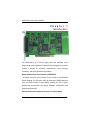
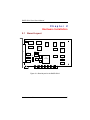
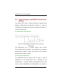
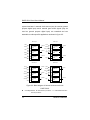
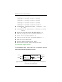
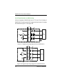
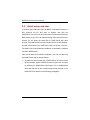
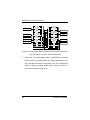
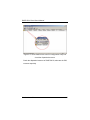
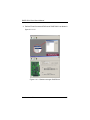
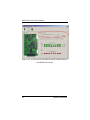
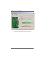
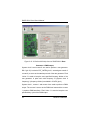
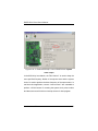
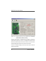
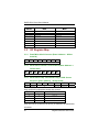
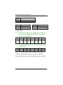
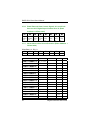
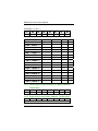
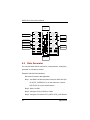
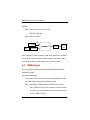
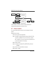
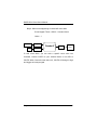
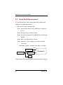
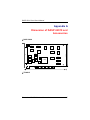
DASP-52010
10 Channel Counter/Timer Card
User’s Manual
Disclaimers
The information in this manual has been carefully checked and is
believed to be accurate. AXIOMTEK Co., Ltd. assumes no
responsibility for any infringements of patents or other rights of third
parties which may result from its use.
AXIOMTEK assumes no responsibility for any inaccuracies that may
be contained in this document. AXIOMTEK makes no commitment to
update or to keep current the information contained in this manual.
AXIOMTEK reserves the right to make improvements to this
document and/or product at any time and without notice.
No part of this document may be reproduced, stored in a retrieval
system, or transmitted, in any form or by any means, electronic,
mechanical, photocopying, recording, or otherwise, without the prior
written permission of AXIOMTEK Co., Ltd.
©Copyright 2004 by Axiomtek Co., Ltd.
All rights reserved.
December 2004, Version A1
Printed in Taiwan
ii
Table of Contents
Chapter 1 Introduction ...................... 1
1.1
Features ............................................................. 2
1.2
Specifications ...................................................... 2
1.3
Accessories......................................................... 5
Chapter 2 Hardware Installation......... 7
2.1
Board Layout....................................................... 7
2.2
Signal Connections.............................................. 8
2.3
Jumper Setting .................................................. 12
2.4
Timer/Counter and DI/DO Circuits and Wiring .... 13
2.5
Quick setup and test .......................................... 17
Chapter 3 Register Structure and
Format ........................... 29
3.1
Overview ........................................................... 29
3.2
I/O Register Map ............................................... 30
Chapter 4 Applications ..................... 37
4.1
Wire Configuration............................................. 37
4.2
Rate Generator ................................................. 38
4.3
PWM Output...................................................... 39
4.4
Square Wave Generator .................................... 40
4.5
32 bits Real-Time Clock..................................... 41
4.6
Frequency Measurement ................................... 42
4.7
Event Counter ................................................... 44
iii
4.8
Pulse Width Measurement ................................. 46
Appendix A Dimension of DASP-52010
and Accessories .............. 47
iv
DASP-52010 Card User’s Manual
Chapter 1
Introduction
The DASP-52010 is a PCI-bus, eight 16-bit two cascaded 32-bit
timer/counter card. It supports 16 general purpose digital I/O channels,
making it suitable for frequency measurement, event counting,
time-delay, and pulse generation applications.
Board Identification- Serial Number on EEPROM
The DASP stores the serial number of each DASP in the EEPROM
before shipping. The PCI scan utility can scan all the DASP and show
users the serial number of each DASP, helping the user to easily
identify and access each card during hardware configuration and
software programming.
Easy to troubleshoot hardware resource- PCI Scan Utility
Introduction
1
DASP-52010 Card User’s Manual
The PCI scan utility can scan all the DASP products within the system,
and can show users all system resources, such as serial numbers,
IRQ, and I/O addresses. This lets users clearly see through and
immediately know whether all DASPs are working normally,
decreasing the time of searching confirmation.
1.1
Features
8 independent 16-bit timer/counter
2 cascade 32-bit timer/counter
8 TTL level D/I & D/O
Jumper selectable interrupt source
Software selectable interrupt source
4 interrupt source- 2 counter & 2 D/I
2 on-board internal clock source
8 external clock source & 8 external gate control signal
Windows® 98/NT/2000/XP and Labview 6.0/7.0 driver
supported.
Complete sample program- VB, VC, BCB, Delphi
1.2
Specifications
Digital Inputs
Input channels: 16 (clock/gate control)
Input type: TTL level
Input voltage:
Low -0.5 ~ 0.8V
High 2.0 ~ 5.2V
Interrupt source: COUT5, COUT7, COUT11, EXT_CLK9 /
2
Introduction
DASP-52010 Card User’s Manual
DI11
Load current: -0.45mA to +70£gA
Digital Outputs
Output channels: 8
Input type: TTL level
Input voltage:
Low -0.5 ~ 0.8V
High 2.0 ~ 5.2V
Sink source: +64mA
Source current: -15mA
Introduction
3
DASP-52010 Card User’s Manual
Timer/Counter
Channels: 8 16-bit independent & 2 32-bit cascaded
Type: TTL level
Programmable clock: 0.5MHz, 1MHz, 2MHz, 4MHz
Programmable counter mode: 12
Max. frequency: 10 HMz
Time based: internal / external clock
General environment
I/O connector type: 37-pin D-sub female
Power consumption:
+5V/500mA (typical),
+5V/600mA (max.)
Operation temperature: 0 ~ 60°C
Storage temperature: -20 to 70°C
Humidity: 0 to 90% non-condensing
Dimensions: 185mm x 122mm
4
Introduction
DASP-52010 Card User’s Manual
1.3
Accessories
To make the DASP-52010 functionality complete, we carry a versatility
of accessories for different user requirements in the following items:
Wiring Cable
CB-89037-2: 37-pin female D-sub type cable with 2m
length
CB-89037-5: 37-pin female D-sub type cable with 5m
length
The shielded D-sub cable with 2m and 5m are designed for the
DASP-52010 I/O connector, respectively.
Terminal Block
TB-88037: D-sub 37P female terminal block with DIN-rail
mounting
The terminal block is directly connected to I/O connector of the
DASP-52010.
Introduction
5
DASP-52010 Card User’s Manual
This page does not contain any information.
6
Introduction
DASP-52010 Card User’s Manual
Chapter 2
Hardware Installation
2.1
Board Layout
JP1
U1
U7
U12
8254
U2
U8
CPLD
U13
8254
U16
8254
U14
U17
8254
U15
U18
RP1
CN1
U3
JP3
CON2
JP2
U4
1
2
3
1
2
3
U6
OSC
U5
U11
PCI Bridge
U19
U10
U20
Figure 2-1: Board layout for the DASP-52010
Hardware Installation
7
DASP-52010 Card User’s Manual
2.2
Signal Connections
Signal Connection Descriptions
DI/O
CON1
DASP-52010
TB-88037
CB-89037-2
CB-89037-5
Figure 2-2: Signal connections for the DASP-52010
Referring to Figure 2-2, the accessories of the DASP-52010 are
depicted in figure 2-3 and described as below.
CON1: The I/O connector CON1 on the DASP-52010 is a
37-pin D-sub female connector for digital input
signals. CON1 enables you to connect to
accessories, the terminal block TB-88037, with the
shielded D-sub cable CB-89037-2 or CB-89037-5.
Digital Input Connector CON1
CON1
8
Hardware Installation
DASP-52010 Card User’s Manual
CB-89037
Hardware Installation
9
DASP-52010 Card User’s Manual
TB-88037
Figure 2-3: DIO signal connections for the DASP-52010
10
Hardware Installation
DASP-52010 Card User’s Manual
The pin assignment of CON1 of DASP-52010 is listed as follows.
D-Sub 37-pin Connector for DASP-52010 CON1
Description
Pin
Pin
Description
Ground
20
1
Ground
EXT_GATE0 / DI4
21
2
EXT_CLK0 / DI0
EXT_GATE1 / DI5
22
3
COUT0
COUT1
23
4
EXT_CLK1 / DI1
EXT_GATE2 / DI6
24
5
EXT_CLK2 / DI2
EXT_GATE3 / DI7
25
6
COUT2
COUT3
26
7
EXT_CLK3 / DI3
EXT_GATE6 / DI12
27
8
EXT_CLK6 / DI8
EXT_GATE7 / DI13
28
9
COUT7
29
10
EXT_CLK7 / DI9
EXT_GATE8 / DI14
30
11
EXT_CLK8 / DI10
EXT_GATE9 / DI15
31
12
COUT8
COUT9
32
13
EXT_CLK9 / DI11
COUT11
33
14
COUT5
DO1
34
15
DO0
DO3
35
16
DO2
DO5
36
17
DO4
DO7
37
18
DO6
19
+5V
COUT6
EXT_CLKn: external clock source for counter n
EXT_GATEn: external gate control signal for counter n
COUTn: output of timer/counter n
DOn: digital output channel n
DIn: digital input channel n
All signals are TTL compatible.
Hardware Installation
11
DASP-52010 Card User’s Manual
2.3
Jumper Setting
2.3.1 JP1 Interrupt Source Selection
There are four signals can be used as interrupt sources: COUT5,
COUT7, COUT11, EXT_CLK9/DI11
1
7
2
8
JP1
Jumper
COUT5
COUT7
COUT11
ECLK9/DI11
JP1
1-2
3-4
5-6
7-8
2.3.2 JP3 PCI Bus Interrupt Setting
JP3
12
JP3
1
1
2
2
3
3
Jumper
LINTi1 (Default)
LINTi2
JP3
1-2
2-3
Hardware Installation
DASP-52010 Card User’s Manual
2.4
Timer/Counter and DI/DO Circuits and
Wiring
The internal clock source, internal timer/counter functional block
diagrams of DASP-52010 are depicted as in figure 2-4 ~ figure 2-6.
The digital input and digital output wirings are depicted as in figure 2-7
to figure 2-8 respectively.
2.4.1 On-board Clock Sources
Figure 2-4: Block diagram of internal clock source for the
DASP-52010
The
DASP-52010
has
2
on-board
internal
clock
sources
SYS_CLOCK0 and SYS_CLOCK1. SYS_CLOCK0 may be software
programmable to 4MHz or 2MHz. SYS_CLOCK1 may be software
programmable to 1MHz or 0.5MHz.
2.4.2 Counter Architecture
The DASP-52010 has four 82c54 chips on board. It offers 8
independent 16 bits timers/counters and 2 cascaded 32 bits
timers/counters. 2 on-board software programmable internal clock
sources provide 4MHz/2MHz and 1MHz/0.5MHz clock signal for
Hardware Installation
13
DASP-52010 Card User’s Manual
system time base. 8 external clock sources (may be used as general
purpose digital input) and 8 external gate control signals (may be
used as general purpose digital input) are contained and can
assemble to realize specific applications as shown in figure 2-5.
8254 Chip 0
CLK0
GATE0
CLK
OUT
Counter0
GATE
COUT0
CLK
OUT
Counter1
GATE
COUT1
CLK
OUT
Counter2
GATE
COUT2
CLK1
GATE1
8254 Chip 1
CLK3
GATE3
SYS_CLOCK
0
CLK
OUT
Counter3
GATE
High
CLK
OUT
Counter4
GATE
High
CLK
OUT
Counter5
GATE
COUT3
CLK2
GATE2
8254 Chip 2
CLK6
GATE6
GATE7
8254 Chip 3
CLK
OUT
Counter6
GATE
COUT6
CLK
OUT
Counter7
GATE
COUT7
CLK
OUT
Counter8
GATE
COUT8
CLK7
COUT5
CLK9
GATE9
SYS_CLOCK
0
CLK
OUT
Counter9
GATE
High
CLK
OUT
Counter10
GATE
High
CLK
OUT
Counter11
GATE
COUT9
CLK8
GATE8
COUT11
Figure 2-5: Block diagram of internal clock source for the
DASP-52010
8 independent 16 bits timer/counter + 2 cascaded 32 bits
timer/counter
14
Hardware Installation
DASP-52010 Card User’s Manual
82c54 chip 0
counter 0 + counter 1 + counter 2
82c54 chip 1
counter 3 + counter 4 + counter 5
82c54 chip 2
counter 6 + counter 7 + counter 8
82c54 chip 3
counter 9 + counter 10 + counter 11
8 independent 16 bits timer/counter
6, 7, 8, 9
2 cascaded 32 bits timer/counter
10+11
counter 0, 1, 2, 3,
counter 4+5, counter
CLK 0,1,2,3,6,7,8,9 refer to I/O Base Address + 6
GATE 0,1,2,3,6,7,8,9 refer to I/O Base Address + 5
Clock1 refer to I/O Base Address + 4
COUT 0,1,2,3,6,7,8,9 refer to I/O Base Address + 6
GATE 4,5,10,11 always High
CLK 4,10 always connect to Sys_Cock0
OUT4 connect to CLK5, OUT10 connect to CLK11
2.4.3 Counter Output Inverter
For convenience using, every COUT wire to connector could be
software programmable cascaded an inverter.
CLK0
GATE0
CLK
OUT
Counter0
GATE
COUT0 from 8254
COUT0 to
Connector
Figure 2-6: Block diagram of software programmable cascaded an
inverter for the DASP-52010
Hardware Installation
15
DASP-52010 Card User’s Manual
2.4.4 Timer/Counter and DIO wrring
All the I/O signals of DASP-52010 are in TTL level. The I/O wiring of
DASP-52010 for both general DIO usage and timer/counter I/O usage
are sketched in figure 2-7 and figure 2-8.
+5V
+5V
TTL
Device
DI+
GND
GND
GND
MCU
Figure 2-7: Digital input wiring diagram for the DASP-52010
+5V
+5V
GND
DO0
TTL
Device
GND
Figure 2-8: Digital output wiring diagram for the DASP-52010
16
Hardware Installation
DASP-52010 Card User’s Manual
2.5
Quick setup and test
To install a new DASP-52010 into an IBM PC compatible computer, at
first, power-off the PC and open its chassis, then plug the
DASP-52010 into a PCI slot of mother-board. Please ensure that (the
BIOS setting of) your PC has released enough IRQ resources for PCI
devices. Do not share the same IRQ of DASP-52010 with other
devices. The DASP-52010 is a plug and play device for MS Windows,
and the OS will detect your DASP-52010 after you power on the PC.
The detail of driver and software installation is described in software
manual of DASP-52010.
After the hardware and software installation, user can emulate and
test DASP-52010 step by step as follows.
1. To perform a full functional test of DASP-52010, we can route the
input and output signals of DASP-52010 as in figure 2-9. And then,
by following the DASP-52010 test branch of the ToolWorkShop
which will fully test all the on-board timer/counter devices of the
DASP-52010 as descried in the following paragraphs.
Hardware Installation
17
DASP-52010 Card User’s Manual
Rate Output
Frequency Input
Event Source
Event Trigger
32 bits Timer
PCB's GND
EXT_CLK0/DI0
COUT0
EXT_CLK1/DI1
EXT_CLK2/DI2
COUT2
EXT_CLK3/DI3
EXT_CLK6/DI8
COUT6
EXT_CLK7/DI9
EXT_CLK8/DI10
COUT8
EXT_CLK9/DI11
COUT5
DO0
DO2
DO4
DO6
PCB's +5V Output
1
2
3
4
5
6
7
8
9
10
11
12
13
14
15
16
17
18
19
20
21
22
23
24
25
26
27
28
29
30
31
32
33
34
35
36
37
PCB's GND
EXT_GATE0/DI4
EXT_GATE1/DI5
COUT1
EXT_GATE2/DI6
EXT_GATE3/DI7
COUT3
EXT_GATE6/DI12
EXT_GATE7/DI3
COUT7
EXT_GATE8/DI4
EXT_GATE9/DI15
COUT19
COUT11
DO1
DO3
DO5
DO7
PWM Output
Square Wave
Output
Pulse Source
32 bits Timer
Figure 2-9: I/O wiring diagram for DASP-52010 full function test (refer
to pin assignment of CON 1 of the DASP-52010)
2. Launch the ‘PCI Configuration Utility’ of DASP-52010 to ensure
that the resource of DASP-52010 is properly dispatched by the
OS. Press the scan button in the toolbar of the ‘PCI Configuration
Utility’ to find the installed DASP-52010, and then check the
resource list as show in figure 2-10.
18
Hardware Installation
DASP-52010 Card User’s Manual
Figure 2-10: Scan DASP-52010 with PCI configuration Utility and
check the dispatched resource
Check the dispatched resource of DASP-52010, take care the IRQ
resource especially.
Hardware Installation
19
DASP-52010 Card User’s Manual
3. Exit the ‘PCI Configuration Utility’ and launch the ‘ToolWorkShop’
for DASP-52010. As shown in figure 2-11.
Figure 2-11: 1 launch ToolWorkShop,
20
2 Select board test
Hardware Installation
DASP-52010 Card User’s Manual
4. Perform Timer/Counter and DIO test of DASP-52010 as shown in
figure 2-113~9.
Figure 2-12: 3 Select test target: DASP52010
Hardware Installation
21
DASP-52010 Card User’s Manual
Figure 2-13: 4 Check device information and press ‘Enable’ button to
load DASP-52010 library
22
Hardware Installation
DASP-52010 Card User’s Manual
Figure 2-14:5 Perform digital input/output test by set the DO port
value and read back the DI port value of DASP-52010
Hardware Installation
23
DASP-52010 Card User’s Manual
Figure 2-15: 6 Perform 8254 chip 0 test of DASP-52010: Rate
Generator & PWM output.
System clock 0 and counter 0 are used to perform a rate generator.
DO 0 (pin 15) is wired to EXT_GATE0 (pin 21, external gate control of
counter 0) to serve as the start/stop control of the rate generator. Filed
‘Value 0’ is used to keep the user specified frequency divider of the
rate generator. A pulse train with frequency of (System clock 0
frequency) / (frequency divider) is available in COUT0 (pin 3).
System clock 1, counter 1 and counter 2 are used to perform a PWM
output. The counter 2 serves as the PWM time base and the counter
1 produces PWM waveform. Filed ‘Value 1’ is used to keep the user
specified duty cycle of the PWM output.
24
Hardware Installation
DASP-52010 Card User’s Manual
Figure 2-16: 7 Perform 8254 chip 1 test of DASP-52010: Square
wave output
In the 8254 chip1 test branch, the Filed ‘Value 3’ is used to keep the
user specified frequency divider of the square wave and the system
clock 0 is used to produce the base frequency of the square wave. In
real-time clock application, counter 4 and counter 5 are cascaded to
perform a 32-bit counter for counting the system clock pulse number
and than sever as a 32-bit timer interrupt source for host program.
Hardware Installation
25
DASP-52010 Card User’s Manual
Figure 2-17: 8 Perform 8254 chip 2 test of DASP-52010: Frequency
measurement & Event counting.
Counter 6 and Counter 7 of DASP-52010 are tested by a frequency
measurement experiment. Counter 7 is configured as a reference time
base for the measurement and Counter 6 is used to count the external
measured signal period base on the reference time interval.
Counter 8 is configured simply to serve as an event count to count the
external event (pulse).
26
Hardware Installation
DASP-52010 Card User’s Manual
Figure 2-18: 9 Perform 8254 chip 3 test of DASP-52010: Pulse width
measurement.
Counter 8 is tested by a pulse-width measurement experiment. The
gate-control of Counter 8 is wired direct to an external pulse source.
When the pulse turn to on and enable the gate-control of the timer,
Counter 8 is initiated to counting base on rate of the System Clock 0
of DASP-52010 until the pulse turn off again. The pulse-width of the
external pulse is then obtained according to the contents of Counter 8
and the period of System Clock 0.
Hardware Installation
27
DASP-52010 Card User’s Manual
5. Before exiting ‘ToolWorkShop’, press ‘Release’ button to release
DASP-52010 library.
All the details of DASP-52010 application used in these test branches
are described in Chapter 4.
28
Hardware Installation
DASP-52010 Card User’s Manual
Chapter 3
Register Structure and Format
3.1
Overview
The DASP-52010 board occupies 25 consecutive I/O address. The
address of each register is defined as the board’s base address plus
an offset. The I/O registers and their corresponding functions are
listed in the followings.
Address
Read
Write
Base + 0x0
Active 82c54 Counter 0
Active 82c54 Counter 0
Base + 0x1
Active 82c54 Counter 1
Active 82c54 Counter 1
Base + 0x2
Active 82c54 Counter 2
Active 82c54 Counter 2
Base + 0x3
Reserved
Active 82c54 Counter
Control Word
Base + 0x4
Digital Input Channel 0-7 or
External GATE 0-3, CLK 0-3
Select SYS_CLOCK0, 1
source and 82c54 Chip
0/1/2/3, Active CLKn setting
Base + 0x5
Digital Input Channel 8-15
or External GATE 6-9, CLK
6-9
Selected 82c54 GATEn
Source
Base + 0x6
Reserved
Select 82c54 CLKn Source
Base + 0x7
Device Label
Digital Output Channel 0-7
Base + 0x8
Reserved
Counter Output Inverter
Control Word Low Byte
Base + 0x9
Reserved
Reserved
Base + 0xA
Reserved
Reserved
Base + 0xB
Reserved
Reserved
Base + 0xC
Reserved
Reserved
Base + 0xD
Reserved
Reserved
Base + 0xE
Reserved
Reserved
Base + 0xF
Reserved
Reserved
Base + 0x10
Reserved
Counter Output Inverter
Control Word High Byte and
Interrupt Control Word
Register Structure and Format
29
DASP-52010 Card User’s Manual
Address
Read
Write
Base + 0x11
Reserved
Reserved
Base + 0x12
Reserved
Reserved
Base + 0x13
Reserved
Reserved
Base + 0x14
Reserved
Reserved
Base + 0x15
Reserved
Reserved
Base + 0x16
Reserved
Reserved
Base + 0x17
Reserved
Reserved
Base + 0x18
Reserved
Clear Interrupt Status
3.2
I/O Register Map
3.2.1
Read/Write 82c54 Counter (Base Address + Offset
0x00-02)
D7
D6
D5
D4
D3
D2
D1
D0
8 bit Counter Data (D0-D7)
3.2.2
Write 82c54 Counter Control Word (Base Address +
Offset 0x03)
D7
D6
D5
D4
D3
D2
D1
D0
8 bit Counter Data (D0-D7)
3.2.3
Write 82c54 Chip 1/2/3/4 and SYS_CLOCK Source
Selection (Base Address + Offset 0x04)
D7
D6
D5
ClkSel1 ClkSel0
D4
X
D3
D2
D1
D0
ActClk
ChpSel1
ChpSel0
Only one 82c54 is selected to access at a moment.
ChpSel1
ChpSel0
Chip Selected
0
0
Chip 0
0
1
Chip 1
1
0
Chip 2
1
1
Chip 3
Only one CLK set (4 82c54 CLK Source) is selected to be switched at
a moment.
30
Register Structure and Format
DASP-52010 Card User’s Manual
ActClk
0
Active CLK 0-3 Source
1
Active CLK 6-9 Source
ClkSel0
ClkSel1
0
SYS_CLOCK0 = 2MHz
0
SYS_CLOCK1 = 0.5MHz
1
SYS_CLOCK0 = 4MHz
1
SYS_CLOCK1 = 1MHz
X: Reserved bit.
3.2.4
Read External Gate Control Signals 0-3 and Clock
Sources 0-3/ Digital Input Channel 0 to 7 (Base
Address + Offset 0x04)
D7
EXT_
D6
EXT_
D5
EXT_
D4
EXT_
D3
EXT_
GATE3/ GATE2/ GATE1/ GATE0/ CLK3/
DI4
DI5
DI6
DI7
DI3
3.2.5
D2
D1
D0
EXT_
EXT_
EXT_
CLK2/
CLK1/
CLK0/
DI2
DI1
DI0
Write 82c54 GATEn Source Selection (Base Address
+ Offset 0x05
D7
GATE7
D6
GATE6
D5
GATE5
D4
GATE4
D3
GATE3
D2
GATE2
D1
GATE1
D0
GATE0
GATEn = 0: GATEn switch to external gate input pin (EGATEn)
GATEn = 1: GATEn switch to OUT of counter n-1 (COUTn-1)
Note: GATE0 can switch to COUT3, GATE6 can switch to COUT9.
Register Structure and Format
31
DASP-52010 Card User’s Manual
3.2.6
Read External Gate Control Signals 6-9 and Clock
Sources 6-9/ Digital Input Channel 8 to 15 (Base
Address + Offset 0x05)
D7
EXT_
D6
EXT_
D5
EXT_
D4
EXT_
D3
EXT_
GATE9/ GATE8/ GATE7/ GATE6/ CLK9/
DI12
DI13
DI14
DI15
DI11
3.2.7
D2
D1
D0
EXT_
EXT_
EXT_
CLK8/
CLK7/
CLK6/
DI10
DI9
DI8
Write 82c54 CLKn Source Selection (Base Address +
Offset 0x06)
When Base + 4, D2 = 0:
D7
CLK3-1
D6
D5
D4
D3
D2
D1
CLK3-0 CLK2-1 CLK2-0 CLK1-1 CLK1-0 CLK0-1 CLK0-0
SYS_CLOCK0
CLK0-1 = 0, CLK0-0 = 0
SYS_CLOCK1 COUTn-1 ECLKn
SYS_CLOCK0
SYS_CLOCK1
CLK0-1 = 0, CLK0-0 = 1
COUT3
CLK0-1 = 1, CLK0-0 = 0
ECLK0
CLK0-1 = 1, CLK0-0 = 1
CLK1-1 = 0, CLK1-0 = 0
SYS_CLOCK0
SYS_CLOCK1
CLK1-1 = 0, CLK1-0 = 1
COUT0
CLK1-1 = 1, CLK1-0 = 0
ECLK1
CLK1-1 = 1, CLK1-0 = 1
CLK2-1 = 0, CLK2-0 = 0
SYS_CLOCK0
SYS_CLOCK1
CLK2-1 = 0, CLK2-0 = 1
COUT1
CLK2-1 = 1, CLK2-0 = 0
ECLK2
CLK2-1 = 1, CLK2-0 = 1
CLK3-1 = 0, CLK3-0 = 0
CLK3-1 = 0, CLK3-0 = 1
CLK3-1 = 1, CLK3-0 = 0
CLK3-1 = 1, CLK3-0 = 1
32
D0
SYS_CLOCK0
SYS_CLOCK1
COUT2
ECLK3
Register Structure and Format
DASP-52010 Card User’s Manual
When Base + 4, D2 = 1:
D7
CLK7-1
D6
D5
D4
D3
D2
D1
CLK7-0 CLK6-1 CLK6-0 CLK5-1 CLK5-0 CLK4-1 CLK4-0
SYS_CLOCK0
CLK4-1 = 0, CLK4-0 = 0
SYS_CLOCK1 COUTn-1 ECLKn
SYS_CLOCK0
SYS_CLOCK1
CLK4-1 = 0, CLK4-0 = 1
COUT9
CLK4-1 = 1, CLK4-0 = 0
ECLK6
CLK4-1 = 1, CLK4-0 = 1
CLK5-1 = 0, CLK5-0 = 0
SYS_CLOCK0
SYS_CLOCK1
CLK5-1 = 0, CLK5-0 = 1
COUT6
CLK5-1 = 1, CLK5-0 = 0
ECLK7
CLK5-1 = 1, CLK5-0 = 1
CLK6-1 = 0, CLK6-0 = 0
SYS_CLOCK0
SYS_CLOCK1
CLK6-1 = 0, CLK6-0 = 1
COUT7
CLK6-1 = 1, CLK6-0 = 0
ECLK8
CLK6-1 = 1, CLK6-0 = 1
CLK7-1 = 0, CLK7-0 = 0
SYS_CLOCK0
SYS_CLOCK1
CLK7-1 = 0, CLK7-0 = 1
COUT8
CLK7-1 = 1, CLK7-0 = 0
ECLK9
CLK7-1 = 1, CLK7-0 = 1
3.2.8
D0
Write Digital Output Channel 0-7 (Base Address +
Offset 0x07)
D7
D6
D5
D4
D3
D2
D1
D0
DO7
DO6
DO5
DO4
DO3
DO2
DO1
DO0
3.2.9
D7
Read Device Label (Base Address + Offset 0x07)
D6
D5
D4
D3
D2
D1
D0
Device Label: 0x0e
Register Structure and Format
33
DASP-52010 Card User’s Manual
3.2.10 Write Counter Output Inverter Control Word Low
Byte (Base Address + Offset 0x08)
D7
D6
D5
INV7
INV6
INV5
D4
X
D3
D2
D1
D0
INV3
INV2
INV1
INV0
INVn = 0: COUTn switch to normal output level (Default after software
installed).
INVn = 1: COUTn cascade to an inverter.
X: Reserved bit
3.2.11 Write Counter Output Inverter Control Word Low
Byte and Interrupt Control (Base Address + Offset
0x10)
D7
D6
D5
D4
D3
D2
D1
D0
EnINT
NeglINT
X
X
INV11
X
INV9
INV8
INVn = 0: COUTn switch to normal output level (Default after software
installed).
INVn = 1: COUTn cascade to an inverter.
NeglINT = 0: Interrupt line output high active.
NeglINT = 1: Interrupt line output low active (Default after software
installed).
EnINT = 0: Disable interrupt (Default after software installed).
EnINT = 1: Enable interrupt.
X: Reserved bit
34
Register Structure and Format
DASP-52010 Card User’s Manual
3.2.12 Write Clear Interrupt Status (Base Address + Offset
0x18)
D7
D6
D5
D4
D3
D2
D1
D0
Write any Value to Clear Interrupt Status
Register Structure and Format
35
DASP-52010 Card User’s Manual
This page does not contain any information.
36
Register Structure and Format
DASP-52010 Card User’s Manual
Chapter 4
Applications
This chapter shows seven typical DASP-52010 application examples:
1. Pulse Output:
a. Rate/ Pulse Generator
b. PWM Output
c. Square Wave Generator
2. 32bits Real-Time Clock
3. Frequency Measurement
4. Event Counter
5. Pulse Width Measurement
4.1
Wire Configuration
Wire configuration for application sample code is given below.
Applications
37
DASP-52010 Card User’s Manual
Application
Demo
Rate Output
Frequency Input
Event Source
Event Trigger
32 bits Timer
PCB's GND
1
EXT_CLK0/DI0
2
COUT0
3
EXT_CLK1/DI1
4
EXT_CLK2/DI2
5
COUT2
6
EXT_CLK3/DI3
7
EXT_CLK6/DI8
8
COUT6
9
EXT_CLK7/DI9
10
EXT_CLK8/DI10
11
COUT8
12
EXT_CLK9/DI11
13
COUT5
14
DO0
15
DO2
16
DO4
17
DO6
18
PCB's +5V Output
19
20
PCB's GND
21
EXT_GATE0/DI4
22
EXT_GATE1/DI5
23
COUT1
24
EXT_GATE2/DI6
25
EXT_GATE3/DI7
26
COUT3
27
EXT_GATE6/DI12
28
EXT_GATE7/DI3
29
COUT7
30
EXT_GATE8/DI4
31
EXT_GATE9/DI15
32
COUT19
33
COUT11
34
DO1
35
DO3
36
DO5
37
DO7
PW M Output
Square W ave
Output
Pulse Source
32 bits Timer
CN1
D-Sub 37 pin
4.2
Rate Generator
You can use DASP-52010 counters for a rate generator, a frequency
generator or a frequency division.
Example: 500 KHz Rate Generator
We select Counter0 to this application.
Step 1: Use DO0 to enable and pause Counter0. Wire DO0 (Pin
15) to EXT_GATE0 (Pin 21) on the connector. Connect
COUT0 (Pin 3) to your external device.
Step 2: Write 0 to DO0.
Step 3: Configure SYS_CLOCK0 to 2 MHz.
Step 4: Configure Counter0 to EXT_GATE0, SYS_CLOCK0 and
38
Applications
DASP-52010 Card User’s Manual
MODE2.
Step 5: Write count value 4 to Counte0.
2 MHz/4 = 500 KHz
Step 6: Write 1 to DO0.
2 MHz
SYS_CLOCK0
C
Counter 0
DO0
EXT_GATE0
O
COUT0
G
External
Device
Every counter is 16 bits. In mode2, valid count value from 2 to 65536
(count value 0 equal to 65536). If want a large count value to get a
low frequency rate, you can cascade two or more counters.
4.3
PWM Output
You can use two counters to provide a simple PWM (Pulse Width
Modulation) output.
Example: PWM Output
We select Counter1 and Counter2 to this application. Counter1
for PWM Output, Counter2 for PWM time base.
Step 1: Use DO2 to enable Counter2. Wire DO2 (Pin 16) to
EXT_GATE2 (Pin 24) on the connector. Connect COUT1
(Pin 23) to your external device. Connect COUT2 (Pin 6)
to EXT_GATE1 (Pin 22).
Register Structure and Format
39
DASP-52010 Card User’s Manual
Step 2: Write 0 to DO2.
Step 3: Configure SYS_CLOCK1 to 0.5 MHz.
Step 4: Configure Counter1 to EXT_GATE1, SYS_CLOCK1 and
MODE1. Configure Counter2 to EXT_GATE2,
SYS_CLOCK1 and MODE2.
Step 5: Write count value 100 to Counte2, 50 to Counte1.
Duty Cycle: 50/100 = 50%
Step 6: Write 1 to DO2.
0.5 MHz
SYS_CLOCK0
C
EXT_GATE1
Counter 1
O
Counter 2
O
COUT1
G
External
Device
0.5 MHz
SYS_CLOCK0
DO2
4.4
EXT_GATE2
C
COUT2
G
Square Wave Generator
You can use DASP-52010 counters to generate a square wave output
for a rate generator, a frequency generator or a frequency division.
Example: 500 KHz Square Wave Generator
We select Counter3 to this application.
Step 1: Use DO3 to enable and pause Counter3. Wire DO3 (Pin
35) to EXT_GATE3 (Pin 25) on the connector. Connect
40
Applications
DASP-52010 Card User’s Manual
COUT3 (Pin 26) to your external device.
Step 2: Write 0 to DO3.
Step 3: Configure SYS_CLOCK0 to 2 MHz.
Step 4: Configure Counter0 to EXT_GATE3, SYS_CLOCK0 and
MODE3.
Step 5: Write count value 4 to Counte3.
2 MHz/4 = 500 KHz
Step 6: Write 1 to DO3.
2 MHz
SYS_CLOCK0
C
Counter 3
DO3
EXT_GATE3
O
COUT3
G
External
Device
Every counter is 16 bits. In mode3, valid count value from 2 to 65536
(count value 0 equal to 65536) and must be even counts. If want a
large count value to get a low frequency rate, you can cascade two or
more counters.
4.5
32 bits Real-Time Clock
DASP-52010 has two 32 bits cascaded timers, counting interval from
1 micro seconds to 2147.48 seconds per tick.
Example: 5 ms RTC Timer Interrupt
We select Counter4, Counter5 to this application.
Register Structure and Format
41
DASP-52010 Card User’s Manual
Step 1: Set interrupt source jumper in COUT5 and set IRQ
jumper to an unused IRQ number. Connect COUT5 (Pin
14) to your external device if necessary.
Step 2: Configure SYS_CLOCK0 to 2 MHz.
Step 3: Configure Counter4, Counter5 to MODE2.
Step 4: Set ISR to IRQn.
Step 5: Write count value 100 to Counte4 and Counter5.
1/2 MHz ×100 ×100 = 5 ms
Step 6: When program ending, unset ISR.
Wired to
SYS_CLOCK0
on-board
2 MHz
Wired to High
on-board
C
Counter 4
O
Counter 5
O
G
C
Wired to High
on-board
Wired to Counter5
Clock Source
on-board
COUT5
G
External
Device
The gate and clock source could set 0 in DLL driver, it is no effect. in
Counter4 ,5, 10, 11.
4.6
Frequency Measurement
You can use two counters to make a roughly frequency measurement.
Example: Frequency Measurement
We select Counter6 and Counter7 to this application, Counter6
42
Applications
DASP-52010 Card User’s Manual
for frequency counter, Counter7 for time base.
Step 1: Use DO6 to enable Counter7. Wire DO6 (Pin 18) to
EXT_GATE7 (Pin 28) on the connector. Wire COUT7
(Pin 29) to EXT_GATE6 (Pin 27) and wire COUT7 (Pin
29) to DI9 (Pin 10). Connect frequency source be
measured to EXT_CLK6 (Pin 8)
Step 2: Configure COUT7 cascaded to an inverter, write 1 to
DO6.
Step 3: Configure SYS_CLOCK1 to 0.5 MHz.
Step 4: Configure Counter6 to EXT_GATE6, EXT_CLK6 and
MODE2. Configure Counter7 to EXT_GATE7,
SYS_CLOCK1 and MODE0.
Step 5: Write count value 49999 to Counte7, 65535 to Counter6.
Time Base: 1/0.5 MHz * (49999 + 1) = 100 ms = 0.1 s
Step 6: Polling DI9 until 100 ms be accomplished.
Step 7: Read in the Counter6 count value.
Frequency = (65535 – Counter6 Value + 1) / 0.1
Register Structure and Format
43
DASP-52010 Card User’s Manual
Frequency Input
EXT_CLK6
C
EXT_GATE6
G
Counter 6
0.5 MHz
SYS_CLOCK0
C
Counter 7
DO6
EXT_GATE7
O
DI9
COUT7
G
In this example, time base is 100 ms. A proper frequency be
measured should faster than 100 KHz (10 ms).
4.7
Event Counter
You can use DASP-52010 counters to count changes of external
signals.
Example: Even Counter
We select Counter8 to this application.
Step 1: Use DO7 to enable and pause Counter0. Wire DO7 (Pin
37) to EXT_GATE8 (Pin 30) on the connector. Connect
EXT_CLK8 (Pin 11) to your event source, COUT8 (Pin 12)
to your external device if necessary.
Step 2: Write 0 to DO7.
Step 3: Configure Counter8 to EXT_GATE8, EXT_CLK8 and
MODE0.
Step 4: Write count value 65535 to Counter8.
Step 5: Write 1 to DO0.
44
Applications
DASP-52010 Card User’s Manual
Step 6: When event happening Counter8 will count down
Event Happen Times = 65535 – Counter8 Count
Value + 1
Event Source
EXT_CLK8
C
Counter 8
DO7
EXT_GATE8
G
O
COUT8
External
Device
If need event alarm, you can write a specific count value into
Counter8, connect COUT8 to your external device or set ISR to
COUT8. When Counter8 count down to 0, COUT8 will change to high
and trigger an interrupt signal.
Register Structure and Format
45
DASP-52010 Card User’s Manual
4.8
Pulse Width Measurement
You can use counter to make a roughly pulse width measurement.
Example: Pulse Width Measurement
We select Counter9 to this application.
Step 1: Connect pulse source to EXT_GATE9 (Pin 31) and DI11
(Pin 13).
Step 2: Configure SYS_CLOCK0 to 4 MHz.
Step 3: Configure Counter9 to EXT_GATE90, SYS_CLOCK0 and
MODE2.
Step 4: Write count value 65535 to Counte9.
Step 5: Polling DI11, if DI11 change to low, read in Counter9
count value.
Pulse Width = (65535 – Counter9 Count Value + 1) /4 MHz
4 MHz
SYS_CLOCK0
C
Counter 9
Pulse Source
EXT_GATE9
G
DI11
In this example, Max. width be measured should short than 16.38 ms.
46
Applications
DASP-52010 Card User’s Manual
Appendix A
Dimension of DASP-52010 and
Accessories
DASP-52010
JP1
U1
U7
U12
8254
U2
U13
8254
U8
CPLD
U16
8254
U14
U17
8254
U15
U18
U3
JP3
CON2
JP2
U4
U5
109
RP1
CN1
1
2
3
1
2
3
U6
OSC
U11
PCI Bridge
U19
U10
U20
185
TB-88037
Dimension of DASP-52010 and Accessories
47
DASP-52010 Card User’s Manual
77
52
112
48
Dimension of DASP-52010 and Accessories