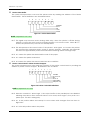
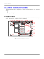
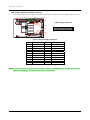
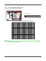
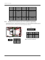
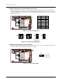
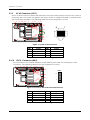
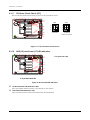
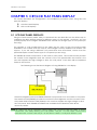
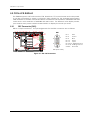
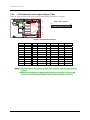
1
IPC Solution
Website: http://www.fabiatech.com
Email: [email protected]
FB-2300 AII-In-One 386SX
CPU CARD Module User’s Manual
Oct 2005
Version: 2.3
Part Number: FB2300
Copyright
©Copyright 2001by FabIATech Corporation. The content of this publication may not be
reproduced in any part or as a whole, transcribed, stored in a retrieval system, translated
into any language, or transcribed in any form or by any means, electronic, mechanical,
magnetic etc. or otherwise without the prior written permission of FabIATech Corporation.
Disclaimer
FabIATech makes no representation of warranties with respect to the contents of this
publication. In an effort to continuously improve the product and add features, FabIATech
reserves the right to revise the publication or change specifications contained in it from
time to time without prior notice of any kind from time to time.
FabIATech shall not be reliable for technical or editorial errors or omissions, which may occur
in this document. FabIATech shall not be reliable for any indirect, special, incidental or
consequential damages resulting from the furnishing, performance, or use of this document.
Trademarks
Trademarks, brand names and products names mentioned in this publication are used for
identification purpose only and are the properties of their respective owners.
Technical Support
If you have problems or difficulties in using the system board, or setting up the relevant
devices, and software that are not explained in this manual, please contact our service
engineer for service, or send email to [email protected].
Returning Your Board For Service & Technical Support
If your board requires servicing, contact the dealer from whom you purchased the product
for service information. You can help assure efficient servicing of your product by following
these guidelines:
! A list of your name, address, telephone, facsimile number, or email address where
you may be reached during the day
! Description of you peripheral attachments
! Description of you software (operating system, version, application software, etc.)
and BIOS configuration
! Description of the symptoms (Extract wording any message)
For updated BIOS, drivers, manuals, or product information, please visit us at
www.fabiatech.com
Static Electricity Precautions
Before removing the board from its anti-static bag, read this section about static electricity
precautions.
Static electricity is a constant danger to the computer systems. The charge that can build up
in your body may be more than sufficient to damage integrated circuits on any PC board. It
is, therefore, important to observe basic precautions whenever you use or handle computer
components. Although areas with humid climates are much less prone to static build-up, it is
always the best to safeguard against accidents, which may result in expensive repairs. The
following measures should generally be sufficient to protect your equipment from static
discharge:
"
Touch a grounded metal object to discharge the static electricity in your body (or
ideally, wear a grounded wrist strap).
"
When unpacking and handling the board or other system components, place all
materials on an antic static surface.
"
Be careful not to touch the components on the board, especially the “golden finger”
connectors on the bottom of every board.
II
Table of contents
FB-2300 AII-IN-ONE 386SX CPU CARD MODULE USER’S MANUAL .......................................................... I
CHAPTER 1 OVERVIEW............................................................................................................................ 1
1.1
1.2
1.3
1.4
INTRODUCTION........................................................................................................................................................... 1
SERIES COMPARISON TABLE ........................................................................................................................................... 1
FEATURES ....................................................................................................................................................................... 2
PACKING LIST............................................................................................................................................................... 3
CHAPTER 2
2.1
2.2
2.3
2.4
2.5
2.6
DMA CONTROLLER ................................................................................................................................................... 5
KEYBOARD CONTROLLER ................................................................................................................................................. 6
INTERRUPT CONTROLLER .................................................................................................................................................. 6
2.4.1 I/O Port Address Map.............................................................................................................................. 7
2.4.2 Real-Time Clock and Non-Volatile RAM......................................................................................... 8
2.4.3 Timer ................................................................................................................................................................ 8
SERIAL PORTS ............................................................................................................................................................... 9
PARALLEL PORTS ............................................................................................................................................................. 11
CHAPTER 3
3.1
3.2
3.3
4.3
HARDWARE FEATURES ....................................................................................................15
BOARD OVERVIEW..................................................................................................................................................... 15
INDEX TO JUMPERS & CONNECTORS .......................................................................................................................... 16
SYSTEM SETTINGS .......................................................................................................................................................... 16
3.3.1 Keyboard/Mouse Connector (CN11 & J9) ................................................................................. 17
3.3.2 PC/104 Connector (CN10 & CN9) .................................................................................................. 20
3.3.3 Hard Disk (IDE) Connector (CN1) .................................................................................................... 23
3.3.4 Reset Header (J3) ................................................................................................................................... 24
3.3.5 Parallel Port Connector (CN3) .......................................................................................................... 24
3.3.6 Auxiliary Power Connectors (J8 & J5 for standalone application) .................................. 25
3.3.7 TTL I/O Connector (CN8) ..................................................................................................................... 26
3.3.8 Serial Ports................................................................................................................................................... 26
3.3.9 RJ-45 Connector (CN7) ........................................................................................................................ 28
3.3.10 CN12- Connector (BNC)...................................................................................................................... 28
3.3.11 CPU Base Clock Select (JP7) ............................................................................................................. 29
3.3.12 HDD (J2) and Power (J7) LED Indicators ...................................................................................... 29
CHAPTER 4
4.1
4.2
SYSTEM CONTROLLERS .................................................................................................... 5
MICROPROCESSOR .......................................................................................................................................................... 5
SOLID STATE DISK.............................................................................................................31
OVERVIEW .................................................................................................................................................................. 31
SWITCH SETTINGS ..................................................................................................................................................... 32
4.2.1 Overview..................................................................................................................................................... 33
4.2.2 SSD and DOC Mapping Address Setting (Switch 1-1, 1-2 & JP4) ...................................... 33
4.2.3 SSD Memory Type Select (Switch 1-4 and JM1 to JM4) ........................................................ 34
PROGRAMMING EPROM/FLASH/SRAM DISK.............................................................................................................. 35
4.3.1 Programming EPROM DISK ................................................................................................................. 35
4.3.2 Programming Flash and SRAM disk................................................................................................. 35
CHAPTER 5
CRT/LCD FLAT PANEL DISPLAY.......................................................................................39
CHAPTER 6
INSTALLATION....................................................................................................................43
5.1
5.2
6.1
6.2
LCD FLAT PANEL DISPLAYS.................................................................................................................................... 39
CRT & LCD DISPLAY ................................................................................................................................................. 40
5.2.1 CRT Connector (DB1) ............................................................................................................................ 40
5.2.2 LCD Connector and Jumper Settings (CN4 ) ............................................................................ 41
INSTALLATION PROCEDURES .......................................................................................................................................... 43
CD ROM ...................................................................................................................................................................... 44
6.2.1 VGA Driver for WIN3.1 ........................................................................................................................... 44
IV
6.3
6.4
6.2.2 LAN Utility..................................................................................................................................................... 44
INTERNAL WATCHDOG TIMER ................................................................................................................................ 45
6.3.1 Watchdog Timer Setting ...................................................................................................................... 45
6.3.2 Watchdog Enabled/Disabled - INDEX 37H ................................................................................. 46
6.3.3 Select Watchdog Report Signal - INDEX 38H ............................................................................. 46
6.3.4 Timeout Status & Reset Watchdog - INDEX 3CH.................................................................................. 46
6.3.5 Programming Watchdog - Basic Operation .............................................................................. 47
PROGRAMMING RS-485 ............................................................................................................................................... 49
CHAPTER 7
7.1
7.2
7.3
7.4
7.5
7.6
7.7
7.8
7.9
7.10
7.11
7.12
7.13
7.14
7.15
BIOS SETUP ........................................................................................................................51
BIOS SETUP OVERVIEW........................................................................................................................................... 51
STANDARD CMOS SETUP ...................................................................................................................................... 53
ADVANCED CMOS SETUP .................................................................................................................................... 55
ADVANCED CHIPSET SETUP ................................................................................................................................. 59
PERIPHERAL SETUP ................................................................................................................................................... 61
AUTO-DETECT HARD DISKS................................................................................................................................... 63
PASSWORD SETTING ............................................................................................................................................... 63
SETTING PASSWORD ...................................................................................................................................................... 63
PASSWORD CHECKING ................................................................................................................................................. 63
LOAD DEFAULT SETTINGS....................................................................................................................................... 64
AUTO CONFIGURATION WITH OPTIMAL SETTINGS ...................................................................................................... 64
7.11.1 Auto Configuration with Fail Safe Settings .................................................................................. 65
BIOS EXIT ...................................................................................................................................................................... 66
SAVE SETTINGS AND EXIT ............................................................................................................................................... 66
EXIT WITHOUT SAVING................................................................................................................................................... 67
BIOS UPDATE .............................................................................................................................................................. 68
APPENDIX......................................................................................................................................................69
A. SPECIFICATIONS ................................................................................................................................................................ 69
B1. PLACEMENT........................................................................................................................................................................ 70
B2. DIMENSIONS ...................................................................................................................................................................... 71
C. EXTERNAL WATCHDOG TIMER ................................................................................................................................................ 72
D1. SRAM MEMORY BANKS ....................................................................................................................................................... 73
D2. SSD TYPE SUPPORTED ........................................................................................................................................................... 74
E. PROGRAMMING TTL I/ O AND GPO0 (1) - BASIC OPERATION ....................................................................................... 76
List of Figures
FB-2300 AII-IN-ONE 386SX CPU CARD MODULE USER’S MANUAL I
CHAPTER 1 ......................................................................................................................... OVERVIEW
......................................................................................................................................................................... 1
1.1
1.2
1.3
1.4
INTRODUCTION........................................................................................................................................................... 1
SERIES COMPARISON TABLE ........................................................................................................................................... 1
FEATURES ....................................................................................................................................................................... 2
PACKING LIST............................................................................................................................................................... 3
CHAPTER 2 ....................................................................................................SYSTEM CONTROLLERS
......................................................................................................................................................................... 5
2.1
2.2
2.3
2.4
2.5
2.6
MICROPROCESSOR .......................................................................................................................................................... 5
DMA CONTROLLER ................................................................................................................................................... 5
KEYBOARD CONTROLLER ................................................................................................................................................. 6
INTERRUPT CONTROLLER .................................................................................................................................................. 6
2.4.1 I/O Port Address Map .............................................................................................................................. 7
2.4.2 Real-Time Clock and Non-Volatile RAM ......................................................................................... 8
2.4.3 Timer................................................................................................................................................................. 8
SERIAL PORTS ............................................................................................................................................................... 9
PARALLEL PORTS ............................................................................................................................................................. 11
CHAPTER 3 .....................................................................................................HARDWARE FEATURES
........................................................................................................................................................................15
3.1
3.2
3.3
BOARD OVERVIEW..................................................................................................................................................... 15
INDEX TO JUMPERS & CONNECTORS .......................................................................................................................... 16
SYSTEM SETTINGS .......................................................................................................................................................... 16
3.3.1 Keyboard/Mouse Connector (CN11 & J9).................................................................................. 17
3.3.2 PC/104 Connector (CN10 & CN9)................................................................................................... 20
3.3.3 Hard Disk (IDE) Connector (CN1) ..................................................................................................... 23
3.3.4 Reset Header (J3) .................................................................................................................................... 24
3.3.5 Parallel Port Connector (CN3)........................................................................................................... 24
3.3.6 Auxiliary Power Connectors (J8 & J5 for standalone application)................................... 25
3.3.7 TTL I/O Connector (CN8) ...................................................................................................................... 26
3.3.8 Serial Ports ................................................................................................................................................... 26
3.3.9 RJ-45 Connector (CN7)......................................................................................................................... 28
3.3.10 CN12- Connector (BNC)...................................................................................................................... 28
3.3.11 CPU Base Clock Select (JP7) ............................................................................................................. 29
3.3.12 HDD (J2) and Power (J7) LED Indicators ...................................................................................... 29
CHAPTER 4 .............................................................................................................SOLID STATE DISK
........................................................................................................................................................................31
4.1
4.2
4.3
OVERVIEW .................................................................................................................................................................. 31
SWITCH SETTINGS ..................................................................................................................................................... 32
4.2.1 Overview...................................................................................................................................................... 33
4.2.2 SSD and DOC Mapping Address Setting (Switch 1-1, 1-2 & JP4)....................................... 33
4.2.3 SSD Memory Type Select (Switch 1-4 and JM1 to JM4) ......................................................... 34
PROGRAMMING EPROM/FLASH/SRAM DISK.............................................................................................................. 35
4.3.1 Programming EPROM DISK .................................................................................................................. 35
4.3.2 Programming Flash and SRAM disk ................................................................................................. 35
CHAPTER 5 ........................................................................................ CRT/LCD FLAT PANEL DISPLAY
........................................................................................................................................................................39
5.1
5.2
LCD FLAT PANEL DISPLAYS.................................................................................................................................... 39
CRT & LCD DISPLAY ................................................................................................................................................. 40
5.2.1 CRT Connector (DB1)............................................................................................................................. 40
VI
5.2.2
LCD Connector and Jumper Settings (CN4 ) ............................................................................. 41
CHAPTER 6 ...................................................................................................................INSTALLATION
........................................................................................................................................................................43
6.1
6.2
6.3
6.4
INSTALLATION PROCEDURES .......................................................................................................................................... 43
CD ROM ...................................................................................................................................................................... 44
6.2.1 VGA Driver for WIN3.1............................................................................................................................ 44
6.2.2 LAN Utility ..................................................................................................................................................... 44
INTERNAL WATCHDOG TIMER ................................................................................................................................ 45
6.3.1 Watchdog Timer Setting....................................................................................................................... 45
6.3.2 Watchdog Enabled/Disabled - INDEX 37H.................................................................................. 46
6.3.3 Select Watchdog Report Signal - INDEX 38H.............................................................................. 46
6.3.4 Timeout Status & Reset Watchdog - INDEX 3CH.................................................................................... 46
6.3.5 Programming Watchdog - Basic Operation............................................................................... 47
PROGRAMMING RS-485 ............................................................................................................................................... 49
CHAPTER 7 ....................................................................................................................... BIOS SETUP
........................................................................................................................................................................51
7.1
7.2
7.3
7.4
7.5
7.6
7.7
7.8
7.9
7.10
7.11
7.12
7.13
7.14
7.15
BIOS SETUP OVERVIEW........................................................................................................................................... 51
STANDARD CMOS SETUP ...................................................................................................................................... 53
ADVANCED CMOS SETUP .................................................................................................................................... 55
ADVANCED CHIPSET SETUP ................................................................................................................................. 59
PERIPHERAL SETUP ................................................................................................................................................... 61
AUTO-DETECT HARD DISKS................................................................................................................................... 63
PASSWORD SETTING ............................................................................................................................................... 63
SETTING PASSWORD ...................................................................................................................................................... 63
PASSWORD CHECKING ................................................................................................................................................. 63
LOAD DEFAULT SETTINGS....................................................................................................................................... 64
AUTO CONFIGURATION WITH OPTIMAL SETTINGS ...................................................................................................... 64
7.11.1 Auto Configuration with Fail Safe Settings .................................................................................. 65
BIOS EXIT ...................................................................................................................................................................... 66
SAVE SETTINGS AND EXIT ............................................................................................................................................... 66
EXIT WITHOUT SAVING................................................................................................................................................... 67
BIOS UPDATE .............................................................................................................................................................. 68
APPENDIX......................................................................................................................................................69
A. SPECIFICATIONS ................................................................................................................................................................ 69
B1. PLACEMENT........................................................................................................................................................................ 70
B2. DIMENSIONS ...................................................................................................................................................................... 71
C. EXTERNAL WATCHDOG TIMER ................................................................................................................................................ 72
D1. SRAM MEMORY BANKS ....................................................................................................................................................... 73
D2. SSD TYPE SUPPORTED ........................................................................................................................................................... 74
E. PROGRAMMING TTL I/ O AND GPO0 (1) - BASIC OPERATION ....................................................................................... 76
List of Tables
Table 2-1 DMA Channel Controller ................................................................................................................5
Table 2-2 Interrupt Controller...........................................................................................................................6
Table 2-3 I/O Port Address Map......................................................................................................................7
Table 2-4 Real-Time Clock & Non-Volatile RAM ...........................................................................................8
Table 2-5 ACE Accessible Registers................................................................................................................9
Table 2-6 Serial Port Divisor Latch .................................................................................................................11
Table 2-7 Registers’ Address ..........................................................................................................................11
Table 3-1 List of Connectors and Jumpers ..................................................................................................16
Table 3-2 CN11 Pin Assignments ...................................................................................................................17
Table 3-3 J9 Pin Assignments .........................................................................................................................18
Table 3-4 Floppy Connector Pin Assignments.............................................................................................19
Table 3-5 CN3: 64-Pin PC/104 Connector Bus A & B..................................................................................20
Table 3-6 CN9 40-Pin PC/104 Connector Bus C & D..................................................................................21
Table 3-7 PC/104 ISA Pin Assignments..........................................................................................................22
Table 3-8 CN1 Hard Disk (IDE) Connector ...................................................................................................23
Table 3-9 CN3: Parallel Port Pin Assignments ..............................................................................................25
Table 3-10 RS-232C Connector .....................................................................................................................26
Table 3-11 CN5 Pin Assignments ...................................................................................................................27
Table 3-12 CN7 RJ-45 Pin Assignments.........................................................................................................28
Table 4-1 SW1-4 SSD Memory Type Select...................................................................................................34
Table 5-1 CN4 LCD Connector Pin Assignments ........................................................................................41
VIII
FabIATech Corporation
CHAPTER 1 OVERVIEW
This chapter provides an overview of your system features and capabilities. The following topics
are covered:
#
#
#
Introduction
Packing List
Features
1.1 INTRODUCTION
The FB2300 series are featured with a compact, all-In-One, mature and well-developed halfsize 386SX CPU card. It provides greater performance such as support for onboard 2MB DRAM
with 6MB expansion capacity, 10Base-T NE2000 compatible network, one RS-232C, PS/2
compatible keyboard and mouse interface, 1 parallel port. It has four sockets of up to
4MB/2MB/SSD or three socket for up to 3MB/1.5MB and one socket for the DiskOnChip® with
up to 288 MB memory capacity.
The FB2300 also comes with a programmable Watchdog timer and other typical interfaces. It
is excellent for embedded systems, MMI’s, workstations, medical applications or POS/POI
systems. As well, an RS-232C/485 port provides the remote control.
Especially, the FB2300 provides CRT and LCD interface with 512KB VRAM on board and uses
the C&T 65545 Chipset, to support a wide range of LCD panels.
1.2 SERIES COMPARISON TABLE
Model
Processor Socket
Chipset
BIOS
Max. DRAM (Def.)
VGA CRT/LCD
VRAM (Max.)
Watchdog Timer
Multi I/O Chip
SSD/DOC Interface
IDE/FDD
2S/1P (RS232/RS485)
Ethernet 10 Mbps
TTL I/O
Expansion PC104
Board Size
FB2300
FB2300A
FB2300C
ALI6117C
ALI6117C
ALI6117C
ALI6117C
ALI6117C
ALI6117C
AMI
AMI
AMI
8MB (2MB)
8MB (2MB)
8MB (2MB)
C&T65545
C&T65545
512KB(1MB)
512KB(1MB)
Yes
Yes
Yes
One
One
One
Yes
Yes
Yes
Yes
Yes
Yes
Yes
Yes
Yes
Yes
Yes
Yes
Yes
Yes
Yes
Yes
185mmx 122mm 185mmx 122mm 185mmx 122mm
FabIATech Corporation
1.3 FEATURES
The system provides a number of special features that enhance its reliability, ensure its
availability, and improve its expansion capabilities, as well as its hardware structure.
#
#
#
#
#
#
#
#
#
#
#
#
#
#
#
#
#
#
Up to 33 MHz 386SX single board computer.
ISA and PC/104 expansion bus.
2 MB EDO RAM on-board & 6 MB space for expansion.
10Base-T NE2000 compatible network. (Without on FB2300A)
Provides CRT and LCD interface with 512KB VRAM. (1MB VRAM is optional)
Parallel port, floppy and IDE Interface.
1 RS-232C and 1 RS-232C/RS485.
PS/2 compatible keyboard and mouse interface.
Provides 4 sockets for up to 4MB/2MB/2MB EPROM/SRAM/Flash disk or 3 sockets for up
to 3MB/1.5MB/1.5MB SSD and 1 socket for DiskOnChip.
4 TTL inputs and 4 TTL outputs.
E2KEY function for safe CMOS data keeping. (Option)
On-board buzzer and LED indicator.
On-board Lithium battery for SRAM disk.
Flash BIOS with easy upgrade utility.
Software programmable watchdog timer.
Low power consumption, +5V only, 2.0A maximum.
EMI Considered on every output signals.
Compact size, 185 mm x 122 mm.
2
FabIATech Corporation
1.4 PACKING LIST
The following accessories are included in the package. Before you begin installing your FB2300
board, take a moment to make sure that they have been included inside the FB2300
package.
#
1 FB2300 all-in-one CPU board
#
1 40-pin hard disk drive interface cable
#
1 34-pin floppy drive interface cable
#
1 parallel port interface and serial port interface cable with bracket
#
1 BNC adapter with FB4616 (Option item)
#
1 PS/2 mouse adapter cable with bracket (Option item)
#
1 CD ROM including necessary utility drivers, quick setting guide file, and this
manual file
NOTE: If any of the listed accessories is missing or damaged, please contact your dealer for
immediate servicing.
FabIATech Corporation
4
FabIATech Corporation
CHAPTER 2 SYSTEM CONTROLLERS
This chapter describes the major structure of the FB2300 CPU board. The following topics are
covered:
#
#
#
#
#
#
Microprocessor
DMA Controller
Keyboard Controller
Interrupt Controller
Serial Ports
Parallel Ports
2.1 MICROPROCESSOR
The FB2300 uses the ALI M6117 CPU; it is designed to perform systems like Intel’s 386SX system
with deep green features.
The 386SX core is the same as M1386SX of Acer Labs. Inc. and 100% object code
compatible with the Intel 386SX microprocessor. System manufacturers can provide 386
CPU based systems optimized for both cost and size. Instruction pipelining and high bus
bandwidth ensure short average instruction execution time and high system throughput.
Furthermore, it can keep the state internally from charge leakage while external clock to the
core is stopped without storing the data in registers. The power consumption here is almost
zero until the clock stops. The internal structure of this core is 32-bit data and address bus with
very low supply current. Real mode as well as Protected mode are available and can run MSDOS /MS-Windows.
2.2 DMA CONTROLLER
The equivalent of two 8237A DMA controllers are implemented in the FB2300 board. Each
controller is a four-channel DMA device that will generate the memory addresses and control
signals necessary to transfer information directly between a peripheral device and memory. This
allows high speeding information transfer with less CPU intervention. The two DMA controllers
are internally cascaded to provide four DMA channels for transfers to 8-bit peripherals (DMA1)
and three channels for transfers to 16-bit peripherals (DMA2). DMA2 channel 0 provides the
cascade interconnection between the two DMA devices, thereby maintaining IBM PC/AT
compatibility.
The following is the system information of DMA channels:
DMA Controller 1
DMA Controller 2
Channel 0: Spare
Channel 4: Cascade for controller 1
Channel 1: Reserved for IBM SDLC Channel 5: Spare
Channel 2: Diskette adapter
Channel 6: Spare
Channel 3: Spare
Channel 7: Spare
Table 2-1 DMA Channel Controller
5
FabIATech Corporation
2.3 KEYBOARD CONTROLLER
The 8042 processor is programmed to support the keyboard serial interface. The keyboard
controller receives serial data from the keyboard, checks its parity, translates scan codes, and
presents it to the system as a byte data in its output buffer. The controller can interrupt the
system when data is placed in its output buffer, or wait for the system to poll its status register
to determine when data is available.
Data can be written to the keyboard by writing data to the output buffer of the keyboard
controller.
Each byte of data is sent to the keyboard controller in series with an odd parity bit
automatically inserted. The keyboard controller is required to acknowledge all data
transmissions. Therefore, another byte of data will not be sent to keyboard controller until
acknowledgment is received for the previous byte sent. The “output buffer full” interruption
may be used for both send-and-receive routines.
2.4 INTERRUPT CONTROLLER
The equivalent of two 8259 Programmable Interrupt Controllers (PIC) are included on the
FB2300 board. They accept requests from peripherals, resolve priorities on pending interrupts in
service, issue interrupt requests to the CPU, and provide vectors which are used as
acceptance indices by the CPU to determine which interrupt service routine to execute.
The following table contains the system information of hardware interrupt priorities:
System Interrupt IRQ Function
Priority
08h
IRQ 0 System timer (Timer Channel 0 output)
1
09h
IRQ1 Keyboard controller output buffer full interrupt
2
0Ah
IRQ 2 Cascade from second programmable interrupt
0Bh
IRQ 3 COM2
10
0Ch
IRQ 4 COM1
11
0Dh
IRQ 5 Parallel port 2
12
0Eh
IRQ 6 Floppy diskette adapter
13
0Fh
IRQ 7 Parallel port 1
14
70h
IRQ 8 Real Time Cock
15
71h
IRQ 9 COM4
3
72h
IRQ 10 LAN adapter
4
73h
IRQ 11 COM3
5
74h
IRQ 12 Reserved for PS/2 mouse
6
75h
IRQ 13 Math coprocessor
7
76h
IRQ 14 Hard diskette adapter
8
77h
IRQ 15 Reserved for Watchdog
9
Table 2-2 Interrupt Controller
6
FabIATech Corporation
2.4.1
I/O Port Address Map
Hex Range
000-01F
020-021
022-023
040-04F
050-05F
060-06F
070-071
080-09F
0A0-0A1
0C0-0DF
0F0
0F1
0F8-0FF
170-178
1F0-1F8
201
208-20A
218-21A
278-27F
2E8-2EF
2F8-2FF
300-31F
320-33F
378-37F
380-38F
3A0-3AF
3B0-3BF
3C0-3CF
3D0-3DF
3E8-3EF
3F0-3F7
3F8-3FF
Device
DMA controller 1
Interrupt controller 1
ALI M6117 chipset address
Timer 1
Timer 2
8042 keyboard/controller
Real-time clock (RTC), non-mask able interrupt (NMI)
DMA page registers
Interrupt controller 2
DMA controller 2
Clear Math Co-processor
Reset Math Co-processor
Math Co-processor
Fixed disk 1
Fixed disk 0
Game port
EMS register 0
EMS register 1
Parallel printer port 2 (LPT 2)
Serial port 4 (COM 4)
Serial port 2 (COM 2)
Prototype card/streaming type adapter
LAN adapter
Parallel printer port 1 (LPT 1)
SDLC, bisynchronous 2
Bisynchronous 1
Monochrome display and printer port 3 (LPT 3)
EGA/VGA adapter
Color/graphics monitor adapter
Serial port 3 (COM 3)
Diskette controller
Serial port 1 (COM 1)
Table 2-3 I/O Port Address Map
7
FabIATech Corporation
2.4.2
Real-Time Clock and Non-Volatile RAM
The FB2300 contains a real-time clock compartment that maintains the date and time in
addition to storing configuration information about the computer system. It contains 14 bytes
of clock and control registers and 114 bytes of general purpose RAM. Because of the use of
CMOS technology, it consumes very little power and can be maintained for long periods of
time using an internal Lithium battery. The contents of each byte in the CMOS RAM are listed
below:
Address
Description
00
Seconds
01
Second alarm
02
Minutes
03
Minute alarm
04
Hours
05
Hour alarm
06
Day of week
07
Date of month
08
Month
09
Year
0A
Status register A
0B
Status register B
0C
Status register C
0D
Status register D
0E
Diagnostic status byte
0F
Shutdown status byte
10
Diskette drive type byte, drive A and B
11
Fixed disk type byte, drive C
12
Fixed disk type byte, drive D
13
Reserved
14
Equipment byte
15
Low base memory byte
16
High base memory byte
17
Low expansion memory byte
18
High expansion memory byte
19-2D
Reserved
2E-2F
2-byte CMOS checksum
30
Low actual expansion memory byte
31
High actual expansion memory byte
32
Date century byte
33
Information flags (set during power on)
34-7F
Reserved for system BIOS
Table 2-4 Real-Time Clock & Non-Volatile RAM
2.4.3
Timer
The FB2300 provides three programmable timers, each with a timing frequency of 1.19 MHz.
Timer 0
The output of this timer is tied to interrupt request 0. (IRQ 0)
Timer 1
This timer is used to trigger memory refresh cycles.
Timer 2
This timer provides the speaker tone. Application programs can load different
counts into this timer to generate various sound frequencies.
8
FabIATech Corporation
2.5 SERIAL PORTS
The ACEs (Asynchronous Communication Elements ACE1 to ACE4) are used to convert parallel
data to a serial format on the transmit side and convert serial data to parallel on the receiver
side. The serial format, in order of transmission and reception, is a start bit, followed by five to
eight data bits, a parity bit (if programmed) and one, one and half (five-bit format only) or two
stop bits. The ACEs are capable of handling divisors of 1 to 65535, and produce a 16x clock for
driving the internal transmitter logic.
Provisions are also included to use this 16x clock to drive the receiver logic. Also included in the
ACE a completed MODEM control capability, and a processor interrupt system that may be
software tailored to the computing time required to handle the communications link.
The following table is a summary of each ACE accessible register
DLAB
0
0
X
X
X
X
X
X
1
1
Register
Port Address
Base + 0
Receiver buffer (read)
Transmitter holding register (write)
Base + 1
Interrupt enable
Base + 2
Interrupt identification (read only)
Base + 3
Line control
Base + 4
MODEM control
Base + 5
Line status
Base + 6
MODEM status
Base + 7
Scratched register
Base + 0
Divisor latch (least significant byte)
Base + 1
Divisor latch (most significant byte)
Table 2-5 ACE Accessible Registers
#
Receiver Buffer Register (RBR)
Bit 0-7: Received data byte (Read Only)
#
Transmitter Holding Register (THR)
Bit 0-7: Transmitter holding data byte (Write Only)
#
Interrupt Enable Register (IER)
Bit 0: Enable Received Data Available Interrupt (ERBFI)
Bit 1: Enable Transmitter Holding Empty Interrupt (ETBEI)
Bit 2: Enable Receiver Line Status Interrupt (ELSI)
Bit 3: Enable MODEM Status Interrupt (EDSSI)
Bit 4: Must be 0
Bit 5: Must be 0
Bit 6: Must be 0
Bit 7: Must be 0
#
Interrupt Identification Register (IIR)
Bit 0: “0” if Interrupt Pending
Bit 1: Interrupt ID Bit 0
Bit 2: Interrupt ID Bit 1
Bit 3: Must be 0
Bit 4: Must be 0
Bit 5: Must be 0
Bit 6: Must be 0
Bit 7: Must be 0
9
FabIATech Corporation
#
Line Control Register (LCR)
Bit 0: Word Length Select Bit 0 (WLS0)
Bit 1: Word Length Select Bit 1 (WLS1)
WLS1
WLS0
Word
Length
5 Bits
6 Bits
7 Bits
8 Bits
0
0
0
1
1
0
1
1
Bit 2: Number of Stop Bit (STB)
Bit 3: Parity Enable (PEN)
Bit 4: Even Parity Select (EPS)
Bit 5: Stick Parity
Bit 6: Set Break
Bit 7: Divisor Latch Access Bit (DLAB)
#
MODEM Control Register (MCR)
Bit 0: Data Terminal Ready (DTR)
Bit 1: Request to Send (RTS)
Bit 2: Out 1 (OUT 1)
Bit 3: Out 2 (OUT 2)
Bit 4: Loop
Bit 5: Must be 0
Bit 6: Must be 0
Bit 7: Must be 0
#
Line Status Register (LSR)
Bit 0: Data Ready (DR)
Bit 1: Overrun Error (OR)
Bit 2: Parity Error (PE)
Bit 3: Framing Error (FE)
Bit 4: Break Interrupt (BI)
Bit 5: Transmitter Holding Register Empty (THRE)
Bit 6: Transmitter Shift Register Empty (TSRE)
Bit 7: Must be 0
#
MODEM Status Register (MSR)
Bit 0: Delta Clear to Send (DCTS)
Bit 1: Delta Data Set Ready (DDSR)
Bit 2: Training Edge Ring Indicator (TERI)
Bit 3: Delta Receive Line Signal Detect (DSLSD)
Bit 4: Clear to Send (CTS)
Bit 5: Data Set Ready (DSR)
Bit 6: Ring Indicator (RI)
Bit 7: Received Line Signal Detect (RSLD)
10
FabIATech Corporation
#
Divisor Latch (LS, MS)
Bit 0:
Bit 1:
Bit 2:
Bit 3:
Bit 4:
Bit 5:
Bit 6:
Bit 7:
LS
Bit 0
Bit 1
Bit 2
Bit 3
Bit 4
Bit 5
Bit 6
Bit 7
MS
Bit 8
Bit 9
Bit 10
Bit 11
Bit 12
Bit 13
Bit 14
Bit 15
Desired Baud Rate
Divisor Used to Generate 16x
Clock
300
384
600
192
1200
96
1800
64
2400
48
3600
32
4800
24
9600
12
14400
8
19200
6
28800
4
38400
3
57600
2
115200
1
Table 2-6 Serial Port Divisor Latch
2.6 PARALLEL PORTS
#
Register Address
Port Address
Read/Write
Register
Base + 0
Write
Output data
Base + 0
Read
Input data
Base + 1
Read
Printer status buffer
Base + 2
Write
Printer control latch
Table 2-7 Registers’ Address
#
Printer Interface Logic
The parallel portion of the SMC37C669 makes the attachment of various devices that accept
eight bits of parallel data at standard TTL level.
#
Data Swapper
The system microprocessor can read the contents of the printer’s Data Latch through the Data
Swapper by reading the Data Swapper address.
11
FabIATech Corporation
#
Printer Status Buffer
The system microprocessor can read the printer status by reading the address of the Printer
Status Buffer. The bit definitions are described below:
7
6
5
4
3
2
1
0
X
X
X
-ERROR
SLCT
PE
-ACK
-BUSY
Figure 2-1 Printer Status Buffer
NOTE: X represents not used.
Bit 7: This signal may become active during data entry, when the printer is off-line during
printing, or when the print head is changing position or in an error state. When Bit 7 is
active, the printer is busy and can not accept data.
Bit 6: This bit represents the current state of the printer’s ACK signal. A 0 means the printer
has received the character and is ready to accept another. Normally, this signal will
be active for approximately 5 microseconds before receiving a BUSY message stops.
Bit 5: A 1 means the printer has detected the end of the paper.
Bit 4: A 1 means the printer is selected.
#
Bit 3: A 0 means the printer has encountered an error condition.
Printer Control Latch & Printer Control Swapper
The system microprocessor can read the contents of the printer control latch by reading the
address of printer control swapper. Bit definitions are as follows:
7
6
X
X
5
4
3
2
1
0
STROBE
AUTO FD XT
INIT
SLDC IN
IRQ ENABLE
DIR(write only)
Figure 2-2 Printer Control Bit Definitions
NOTE: X represents not used.
Bit 5: Direction control bit. When logic 1, the output buffers in the parallel port are disabled
allowing data driven from external sources to be read; when logic 0, they work as a
printer port. This bit is writing only.
Bit 4: A 1 in this position allows an interrupt to occur when ACK changes from low state to
high state.
Bit 3: A 1 in this bit position selects the printer.
12
FabIATech Corporation
Bit 2: A 0 starts the printer (50 microseconds pulse, minimum).
Bit 1: A 1 causes the printer to line-feed after a line is printed.
Bit 0: A 0.5 microsecond minimum highly active pulse clocks data into the printer. Valid data
must be present for a minimum of 0.5 microseconds before and after the strobe pulse.
13
FabIATech Corporation
14
FabIATech Corporation
CHAPTER 3 HARDWARE FEATURES
This section describes the pin assignments for system’s external connectors and the jumper
settings.
#
#
Board Overview
System Setting
3.1 BOARD OVERVIEW
The FB2300 is an all-in-one, half-size, 386SX CPU board. This section provides hardware jumper
settings, the connectors’ locations, and the pin assignment.
J2
J3
JP1
CN4 CN1
J5
J6 CN2
J7 CN3
J4
CN5
BZ1
BAT1
M1
J1
JP2
JP3
JP4
LM1LM2LM3LM4
DB1
M2
SW1
CN12
CN10
JP6
JP7
DB2
CN7
M3
M4
LED1
DB3
CN8
J8
CN9
J9
Figure 3-1 System Components Overview
15
CN11
FabIATech Corporation
3.2 INDEX TO JUMPERS & CONNECTORS
The following lists the jumper and connector functions for reference.
Label
Function
BZ1
Onboard Buzzer
CN1
40-pin 2.54mm IDE hard disk connector
CN2
34-pin 2.54mm floppy connector
CN3
26-pin 2.54mm parallel port connector
CN4
2.0mm 44-pin LCD connector
CN5
10-pin 2.54mm IDC connector for COM2
CN7
RJ45 LAN connector
CN8
10-pin TTL I/O connector
CN9
40-pin PC/104 bus C&D connector
CN10
64-pin PC/104 bus A&B connector
CN11
Standard P/S2 type keyboard/ mouse connector
CN12
10 pin to BNC FB4616 board connector
DB1
15-pin CRT connector
DB3
9-pin DB9 RS-232C serial port for COM1
J1
2-pin external battery connector for SRAM disk
J2
2-pin hard disk LED header
J3
2-pin reset header
J4
3-pin 2.0mm extra RS-232C JST header
J5
9-pin auxiliary power connector
J6
4-pin external speaker header
J7
3-pin power LED header
J8
4-pin auxiliary power connector
J9
PS/2 keyboard & mouse connector
JP1
M/DE Select signal for TFT LCD
JP2
3-pin RS485 terminator
JP3
3x3 jumper to select CN5 RS-485 function
JP4
2x3 SSD and DOC select
JP6
PS/2 mouse function select
JP7
2x3 CPU base clock select jumper
SW1-1 & 1-2, JP4 SSD and DOC mapping address settings
SW1-3
SSD drive select
SW1-4 and JM1 – SSD memory type select
JM4
LED1
Internal Power LED
Table 3-1 List of Connectors and Jumpers
3.3 SYSTEM SETTINGS
Jumper pins allow you to set specific system parameters. Set them by changing the pin
location of jumper blocks. (A jumper block is a small plastic-encased conductor [shorting plug]
that slips over the pins.) To change a jumper setting, remove the jumper from its current
location with your fingers or small needle-nosed pliers. Place the jumper over the two pins
designated for the desired setting. Press the jumper evenly onto the pins. Be careful not to
bend the pins.
We will show the locations of the FB2300 jumper pins, and the factory-default settings.
CAUTION: Do not touch any electronic component unless you are safely grounded. Wear a
grounded wrist strap or touch an exposed metal part of the system unit chassis. The
static discharges from your fingers can permanently damage the electronic
components.
16
FabIATech Corporation
3.3.1
Keyboard/Mouse Connector (CN11 & J9)
(1) 6-Pin Mini DIN Keyboard/Mouse Connector (CN11)
The keyboard/mouse connector is a Mini-DIN 6-pin connector, labeled CN11. It is a PS/2 type
connector and is also used for a standard IBM-compatible keyboard with a keyboard adapter
cable. The pin assignments for the PS/2 port connector are as follows.
J2
J3
JP1
CN4 CN1
J5
J6 CN2
J7 CN3
J4
CN5
BZ1
BAT1
M1
J1
JP2
JP3
JP4
LM1LM2LM3LM4
DB1
M2
SW1
CN12
CN10
JP6
JP7
1
DB2
3
4
CN9
J9
6
5
DB3
CN8
J8
2
CN7
M3
M4
LED1
CN11
Front View
Figure 3-2 Front View of CN11 Mini-Din Connector
Pin
1
2
3
4
5
6
Signal
Keyboard Data
Mouse Data
Ground
VCC
Keyboard Clock
Mouse Clock
Table 3-2 CN11 Pin Assignments
17
FabIATech Corporation
(2) 6-Pin JST Keyboard/Mouse Connector (J9) & PS/2 Function Enable Jumper (JP6)
The following demonstrates the pin assignments of the 6-pin JST keyboard/mouse connector.
To use the PS/2 mouse, an optional adapter cable has to be connected to the J9 (6-pin
header type) connector. The pin assignments for the JST connector are as follows. JP6 is used
to enable or to disable the J9 function.
J2
J3
JP1
CN4 CN1
J5
J6 CN2
J7 CN3
J4
CN5
BZ1
BAT1
M1
J1
JP2
JP3
JP4
LM1LM2LM3LM4
LED1
J9
DB2
DB1
M2
CN7
M3
M4
SW1
CN12
CN10
CN9
JP6
J9
Pin 5: Mouse Clock
1
CN11
JP6
1
Pin 2: Keyboard Data
Pin 4: VCC
CN8
J8
Pin 1: Mouse Data
Pin 3: Ground
DB3
JP6
JP7
6
1
Enable PS/2 Mouse Disable PS/2 Mouse
Factory Preset
Figure 3-3 J9: 6-Pin JST Keyboard Connector
Pin
Signal
1
Mouse Data
2
Keyboard Data
3
Ground
4
VCC
5
Mouse Clock
6
Keyboard Clock
Table 3-3 J9 Pin Assignments
18
Pin 6: Keyboard Clock
FabIATech Corporation
CN2 34-pin 2.54mm IDC Floppy Connector
One 34-pin floppy drive interface cable is provided to connect to the floppy drive device.
J2
J3
JP1
CN4 CN1
J5
J6 CN2
J7 CN3
J4
CN5
BZ1
BAT1
M1
J1
JP2
JP3
JP4
LM1LM2LM3LM4
DB1
M2
SW1
CN12
CN10
JP6
JP7
CN2 –Floppy connector
DB2
33
1
34
2
CN7
M3
M4
LED1
DB3
CN8
J8
CN9
J9
CN11
Figure 3-4 CN2 Floppy Connector
34-pin
Signal
34-pin
Signal
Others No Connection
2
Drive Enable A
22
-Write Data
8
-Index
23
Ground
9
Ground
32
-Head
10
-Motor B
30
-Read Data
11
Ground
26
-Track 0
12
-Select A
24
-Write Enable
14
- Select B
29
Ground
16
-Motor A
28
-Write Protect
18
-Direction
34
-Disk Change
20
-Step
31
Ground
Table 3-4 Floppy Connector Pin Assignments
Note: the included floppy cable supports 720KB, 1.44MB, and 2.88MB floppy disk drives and these
disk drives 360KB and 1.2MB disk drives are not supported.
19
FabIATech Corporation
3.3.2
PC/104 Connector (CN10 & CN9)
(1) 64 Pin PC/104 Connector Bus A & B (CN10)
J2
J3
JP1
CN4 CN1
J5
J6 CN2
J7 CN3
J4
CN5
BZ1
BAT1
M1
J1
JP2
JP3
JP4
LM1LM2LM3LM4
DB1
M2
SW1
CN12
CN10
JP6
JP7
CN10 – BUS A & B
DB2
CN7
M3
M4
LED1
DB3
CN8
J8
CN9
J9
CN11
Figure 3-5 CN10: 64-Pin PC/104 Connector Bus A & B
Pin
1
3
5
7
9
11
13
15
17
19
21
23
25
27
29
31
Signal
Pin
Signal
Signal
Pin
Signal
Pin
-IOCHK 33
SA14
2
Ground 34 -DACK1
SD7
35
SA13
4
RSTDRV 36
DRQ1
SD6
37
SA12
6
+5V
38
-REFSH
SD5
39
SA11
8
IRQ9
40 BUSCLK
SD4
41
SA10
10 -5V (*1) 42
IRQ7
SD3
43
SA9
12
DRQ2
44
IRQ6
SD2
45
SA8
14 -12V (*1) 46
IRQ5
SD1
47
SA7
16
-ZWS
48
IRQ4
SD0
49
SA6
18
+12V
50
IRQ3
IORDY
51
SA5
20
Key1
52 -DACK2
AEN
53
SA4
22 -MEMW 54
TC
SA19
55
SA3
24 -MEMR 56
ALE
SA18
57
SA2
26
-IOW
58
+5V
SA17
59
SA1
28
-IOR
60
OSC
SA16
61
SA0
30 -DACK3 62 Ground
SA15
63 Ground 32
DRQ3
64 Ground
Table 3-5 CN10: 64-Pin PC/104 Connector Bus A & B
NOTE: Power input, +5V, -5V, +12V, or –12V for Pin 10 & Pin14 is supplied from the system power
connected to the power connector.
20
FabIATech Corporation
(2) 40 Pin PC/104 Connector Bus C & D (CN9)
J2
J3
JP1
CN4 CN1
J5
J6 CN2
J7 CN3
J4
CN5
BZ1
BAT1
M1
J1
JP2
JP3
JP4
LM1LM2LM3LM4
DB1
M2
SW1
CN12
CN10
JP6
JP7
CN9 – BUS C & D
DB2
CN7
M3
M4
LED1
DB3
CN8
J8
CN9
J9
CN11
Figure 3-6 CN9: 40-Pin PC/104 Connector Bus C & D
Pin
Signal
1
Ground
3
-SBHE
5
LA23
7
LA22
9
LA21
11
LA20
13
LA19
15
LA18
17
LA17
19 MEMRD16
Pin
21
23
25
27
29
31
33
35
37
39
Signal
MEMWR16
SD8
SD9
SD10
SD11
SD12
SD13
SD14
SD15
Key2
Pin Signal Pin Signal
2 Ground 22 -DACK5
4 -MEM16 24
DRQ5
6
-IO16
26 -DACK6
8
IRQ10
28
DRQ6
10
IRQ11
30 -DACK7
12
IRQ12
32
DRQ7
14
IRQ15
34
+5V
16
IRQ14
36 -MASTER
18 -DACK0 38 Ground
20
DRQ0
40 Ground
Table 3-6 CN9 40-Pin PC/104 Connector Bus C & D
21
FabIATech Corporation
(3) PC/104 (ISA) Signal Description
Name
BUSCLK [Output]
RSTDRV [Output]
SA0 - SA19 [Input / Output]
LA17 - LA23 [Input/Output]
SD0 - SD15 [Input/Output]
ALE [Output]
-IOCHCK [Input]
IORDY [Input, Open collector]
IRQ 3-7, 9-12, 14, 15 [Input]
-IOR [Input/Output]
-IOW [Input/Output]
-SMEMR [Output]
-MEMR 16 [Input/Output]
-MEMW [Output]
-MEMW [Input/Output]
DRQ 0-3, 5-7 [Input]
-DACK 0-3, 5-7 [Output]
AEN [output]
-REFSH [Input/Output]
TC [Output]
-SBHE [Input/Output]
-MASTER [Input]
-MEM16[Input,Open
collector]
-IO16 [Input, Open collector]
OSC [Output]
-ZWS [Input, Open collector]
Description
The BUSCLK signal of the I/O channel is asynchronous to the CPU clock.
This signal goes high during power-up, low line-voltage or hardware reset
The System Address lines run from bit 0 to 19. They are latched onto the
falling edge of "BALE"
The Unlatched Address line run from bit 17 to 23
System Data bit 0 to 15
The Buffered Address Latch Enable is used to latch SA0 – SA19 onto the
falling edge. This signal is forced high during DMA cycles
The I/O Channel Check is an active low signal which indicates that a parity
error exist on the I/O board
This signal lengthens the I/O, or memory read/write cycle, and should be
held low with a valid address
The Interrupt Request signal indicates I/O service request attention. They are
prioritized in the following sequence: (Highest) IRQ 9, 10, 11, 12, 13, 15, 3, 4, 5,
6, 7 (Lowest)
The I/O Read signal is an active low signal which instructs the I/O device to
drive its data onto the data bus
The I/O write signal is an active low signal which instructs the I/O device to
read data from the data bus
The System Memory Read is low while any of the low 1mega bytes of
memory are being used
The Memory Read signal is low while any memory location is being read
The System Memory Write is low while any of the low 1mega bytes of
memory is being written
The Memory Write signal is low while any memory location is being written
DMA Request channels 0 to 3 are for 8-bit data transfers. DMA Request
channels 5 to 7 are for 16-bit data transfers. DMA request should be held
high until the corresponding DMA has been completed. DMA request priority
is in the following sequence:(Highest) DRQ 0, 1, 2, 3, 5, 6, 7 (Lowest)
The DMA Acknowledges 0 to 3, 5 to 7 are the corresponding acknowledge
signals for DRQ 0 to 3 and 5 to 7
The DMA Address Enable is high when the DMA controller is driving the
address bus. It is low when the CPU is driving the address bus
This signal is used to indicate a memory refresh cycle and can be driven by
the microprocessor on the I/O channel
Terminal Count provides a pulse when the terminal count for any DMA
channel is reached
The System Bus High Enable indicates the high byte SD8 - SD15 on the data
bus
The MASTER is the signal from the I/O processor which gains control as the
master and should be held low for a maximum of 15 microseconds or system
memory may be lost due to the lack of refresh
The Memory Chip Select 16 indicates that the present data transfer is a 1wait state, 16-bit data memory operation
The I/O Chip Select 16 indicates that the present data transfer is a 1-wait
state, 16-bit data I/O operation
The Oscillator is a 14.31818 MHz signal
The Zero Wait State indicates to the microprocessor that the present bus
cycle can be completed without inserting additional wait cycle
Table 3-7 PC/104 ISA Pin Assignments
22
FabIATech Corporation
3.3.3
Hard Disk (IDE) Connector (CN1)
A 40-pin header type connector (CN1) is provided to interface with up to two embedded
hard disk drives (IDE AT bus). This interface, through a 40-pin cable, allows the user to connect
up to two drives in a “daisy chain” fashion. To enable or disable the hard disk controller,
please use BIOS Setup program to select. The following table illustrates the pin assignments of
the hard disk drive’s 40-pin connector.
J2
J3
JP1
CN4 CN1
J5
J6 CN2
J7 CN3
BAT1
M1
CN1 – Hard disk connector
J4
CN5
BZ1
JP2
JP3
JP4
LM1LM2LM3LM4
LED1
39
1
40
2
1
J1
DB1
M2
CN7
M3
M4
SW1
CN12
CN10
JP6
JP7
DB2
2
DB3
CN8
J8
CN9
J9
CN11
Figure 3-7 CN1 Hard Disk (IDE) Connector
Pin
Signal
Pin
Signal
1
-RESET
2
Ground
3
DATA 7
4
DATA 8
5
DATA 6
6
DATA 9
7
DATA 5
8
DATA 10
9
DATA 4
10
DATA 11
11
DATA 3
12
DATA 12
13
DATA 2
14
DATA 13
15
DATA 1
16
DATA 14
17
DATA 0
18
DATA 15
19
Ground
20
Ground
21
Not Used
22
Ground
23
-IOW A
24
Ground
25
-IOR A
26
Ground
27
-CHRDY A
28
DALE
29
Not Used
30
Ground
31
-IRQ 14
32
-IO16
33
SA 1
34
Not Used
35
SA 0
36
SA 2
37
CS 0
38
CS 1
39
HD LED A
40
Ground
Table 3-8 CN1 Hard Disk (IDE) Connector
23
FabIATech Corporation
3.3.4
Reset Header (J3)
J3 is used to connect to an external reset switch. Shorting these two pins will reset the system.
J2
J3
JP1
CN4 CN1
J5
J6 CN2
J7 CN3
J4
CN5
BZ1
BAT1
M1
J1
JP2
JP3
JP4
LM1LM2LM3LM4
LED1
J3
DB1
M2
SW1
CN12
CN10
DB3
JP6
CN8
J8
JP7
2: Reset1: Reset+
CN7
M3
M4
DB2
J9
CN9
CN11
Figure 3-8 J3 Reset Header
3.3.5
Parallel Port Connector (CN3)
Use the included adapter cable to connect the 26-pin header type CN3. This adapter cable
is mounted on a bracket and is included in your FB2300 package. The connector for the
parallel port is a 25 pin D-type female connector.
The following table shows signal
connections between 26-pin & DB25 connectors.
J2
J3
JP1
CN4 CN1
J5
J6 CN2
J7 CN3
BZ1
BAT1
M1
J1
JP2
JP3
JP4
LM1LM2LM3LM4
SW1
CN12
CN10
JP6
JP7
DB2
26
CN7
M3
M4
25
DB3
CN8
J8
CN9
J9
CN3
1
LED1
DB1
M2
J4
CN5
CN11
Figure 3-9 CN3 Parallel Port Connectors
24
2
FabIATech Corporation
CN3
1
3
5
7
9
11
13
15
17
19
21
23
25
3.3.6
Signal
CN3
DB-25
Signal
DB-25
1
-STROBE
2
14
-AUTO FORM FEED
2
DATA 0
4
15
-ERROR
3
DATA 1
6
16
-INITIALIZE
4
DATA 2
8
17
-PRINTER SELECT IN
5
DATA 3
10
18
Ground
6
DATA 4
12
19
Ground
7
DATA 5
14
20
Ground
8
DATA 6
16
21
Ground
9
DATA 7
18
22
Ground
10 -ACKNOWLEDGE
20
23
Ground
11
BUSY
22
24
Ground
12
PAPER
24
25
Ground
13 PRINTER SELECT
26
-No Used
Table 3-9 CN3: Parallel Port Pin Assignments
Auxiliary Power Connectors (J8 & J5 for standalone application)
The FB2300 provides two types of power connectors. J8 is a 4-pin 5V power connector. J5 is a
9-pin power connector. Using either of the connectors, you can connect the power supply to
the on board power connector for stand alone applications directly.
J2
J3
JP1
CN4 CN1
J5
J6 CN2
J7 CN3
BZ1
BAT1
M1
J1
JP2
JP3
JP4
LM1LM2LM3LM4
SW1
CN12
CN10
JP6
J8
JP7
DB3
CN8
CN9
J9
CN11
1
9
DB2
CN7
M3
M4
LED1
DB1
M2
J5
J4
CN5
J5
1
2
3
4
5
Signal
+5V
+5V
Ground
Ground
+12V
J5
6
7
8
9
Signal
Ground
Ground
+5V
+5V
J8
1
4
J8
1
2
3
4
Signal
+5V
Ground
Ground
+12V
Figure 3-10 Power Connectors
25
FabIATech Corporation
3.3.7
TTL I/O Connector (CN8)
CN8 is a 2x5 TTL I/O connector and supports 4 TTL outputs and inputs.
J2
J3
JP1
CN4 CN1
J5
J6 CN2
J7 CN3
J4
CN5
BZ1
BAT1
JP2
JP3
JP4
LM1LM2LM3LM4
M1
J1
10
9
2
1
LED1
DB2
DB1
M2
CN7
M3
SW1
CN12
CN10
M4
DB3
JP6
CN8
J8
JP7
CN8
J9
CN9
CN11
Pin 1: INP0
Pin 2:
OUT0
Pin 3: INP1
Pin 4:
OUT1
Pin 5: INP2
Pin 6:
OUT2
Pin 7: INP3
Pint 8: OUT3
Pin 9: +5V
Pin 10: Ground
Figure 3-11 CN8 TTL Connector
3.3.8
Serial Ports
(1) RS-232C Pin Definitions (DB3 and CN5)
DB3 is standard DB9 serial port connector for COM1 and CN5 is 10-pin 2.54mm IDC
connector for COM2. The included serial port adapter cables are used to transfer CN5
connector into standard DB9 connector.
J2
J3
JP1
CN4 CN1
J5
J6 CN2
J7 CN3
BAT1
M1
J1
JP2
JP3
JP4
LM1LM2LM3LM4
SW1
CN12
CN10
JP6
JP7
DB2
9
CN9
J9
6
DB3
CN8
J8
5
CN7
M3
M4
LED1
DB1
M2
DB3
J4
CN5
BZ1
1
CN11
Figure 3-12 DB3 and CN5 RS232C Connectors
The following left table shows DB3’s signal connections and the following right table
shows signal connections of the included cable:
Signal
DB3
CN5
Signal
DB3
-DCD1
1
1
-DCD2
1
-DSR1
6
2
-DSR2
6
RXD1
2
3
RXD2
2
-RTS1
7
4
-RTS2
7
TXD1
3
5
TXD2
3
-CTS1
8
6
-CTS2
8
-DTR1
4
7
-DTR2
4
-RI1
9
8
-RI2
9
Ground
5
9
Ground
5
10 Case Ground
Table 3-10 RS-232C Connector
26
FabIATech Corporation
(2) RS-485 Jumper Select and Pin Definitions (JP2 & JP3)
When RS-485 mode is selected, the RS-485 signals use the same connector as RS-232C.
JP2 is the terminator on/off jumper only when using RS-485 mode. JP3 is used to set up the
RS-232C and RS-485 for the CN5. The following figure and table guide you how to set up
RS-485 serial port.
J2
J3
JP1
CN4 CN1
J5
J6 CN2
J7 CN3
BAT1
JP2
JP3
JP4
LM1LM2LM3LM4
M1
J1
LED1
DB2
DB1
M2
CN7
M3
SW1
CN12
CN10
M4
DB3
JP6
CN8
J8
JP7
CN9
J9
Signal
485485+
-
CN5
1
2
3
4
5
6
7
8
9
J4
CN5
BZ1
CN11
DB9
1
6
2
7
3
8
4
9
5
Table 3-11 CN5 Pin Assignments
JP3
JP3
JP2
1
1
RS-232C
JP2
1
1
Terminator On
Terminator Off
RS-485
Factory Preset
Figure 3-13 JP2 and JP3 RS-485 Select
(3) Extra RS-232C Header (J4: 3-pin 2.0mm JST)
Header J4 provides basic RS-232C signals of serial port 2. It is used to interface with touch
screen module or other internal connection usage.
J2
J3
JP1
CN4 CN1
J5
J6 CN2
J7 CN3
J4
CN5
BZ1
BAT1
M1
J1
JP2
JP3
JP4
LM1LM2LM3LM4
CN7
M3
SW1
CN12
CN10
JP6
JP7
J4
DB2
DB1
M2
M4
LED1
3
DB3
CN8
J8
CN9
J9
CN11
Figure 3-14 J4 RS-232C Header
27
1
Pin 1: TXD2
Pin 2: RXD2
Pin 3: Ground
FabIATech Corporation
3.3.9
RJ-45 Connector (CN7)
CN7 is an RJ45 connector with 2 LED indicators. The upper LED (orange) is lit when the system is
accessing data. The lower LED (green) is lit when power is supplied normally or it blinks when
the watchdog is enabled. The following table lists the pin assignment of CN7.
J2
J3
JP1
CN4 CN1
J5
J6 CN2
J7 CN3
J4
CN5 -
BZ1
BAT1
JP2
JP3
JP4
LM1LM2LM3LM4
M1
J1
LED1
8
M2
CN7
M3
SW1
CN12
CN10
M4
DB3
JP6
CN8
J8
JP7
1
DB2
DB1
J9
CN9
CN11
Figure 3-15 CN7 RJ-45 Connector
CN7
1
2
3
4
3.3.10
Signal
CN7
Signal
TPTX+
5
Not Used
TPTX 6
TPRX TPRX+
7
Not Used
Not Used
8
Not Used
Table 3-12 CN7 RJ-45 Pin Assignments
CN12- Connector (BNC)
It is necessary to use the BNC adapter board (FB4616) and cable for attaching to CN12
connector. The following table lists the pin assignment of CN12.
J2
J3
JP1
CN4 CN1
J5
J6 CN2
J7 CN3
J4
CN5
BZ1
BAT1
M1
J1
JP2
JP3
JP4
LM1LM2LM3LM4
DB1
M2
SW1
CN12
CN10
JP6
JP7
DB2
10
9
2
1
CN7
M3
M4
CN12
LED1
DB3
CN8
J8
CN9
J9
CN11
Figure 3-16 CN12 to BNCFB4616 board Connector
CN12
1
3
5
7
9
Signal
CN12
Signal
LCD+
2
LCDVCC
4
GND
LRX+
6
LRXGND
8
BNCEN
LTPX+
10
LPTXTable 3-13 CN12 Pin Assignment
28
FabIATech Corporation
3.3.11
CPU Base Clock Select (JP7)
The CPU base clock (Input clock) is twice of its operation clock.
J2
J3
JP1
CN4 CN1
J5
J6 CN2
J7 CN3
J4
CN5
BZ1
BAT1
M1
J1
JP2
JP3
JP4
LM1LM2LM3LM4
DB2
DB1
M2
CN7
M3
M4
SW1
CN12
CN10
DB3
JP6
5
6
5
4
3
4
3
2
1
2
1
6
25.0MHz
CN8
J8
JP7
JP7
JP7
LED1
CN9
J9
33.3MHz
Factory Preset
CN11
Figure 3-17 JP7: CPU Base Clock Select
3.3.12
J2
HDD (J2) and Power (J7) LED Indicators
J3
JP1
CN4 CN1
J5
J6 CN2
J7 CN3
J4
CN5
BZ1
BAT1
M1
J1
JP2
JP3
JP4
LM1LM2LM3LM4
DB1
M2
SW1
CN12
CN10
JP6
JP7
DB2
CN7
M3
M4
J7 3-pin Power LED
LED1
DB3
CN8
J8
CN9
J9
CN11
J2 2-pin Hard Disk LED
Figure 3-18 Onboard LED Indicators
#
#
On-Board Power LED indicator: LED1
LED1 is lit yellow when power is connected to the system.
Rear Panel LED Indicators: LM1
LM1 is located on the rear panel with three LED indicators.
29
FabIATech Corporation
30
FabIATech Corporation
CHAPTER 4 SOLID STATE DISK
The section describes the various types of solid-state disk. The following topics are covered:
$
$
$
$
$
Overview
Switch Setting
Jumper Setting
Programming Flash & SRAM Disk
SSD Type Supported
4.1 OVERVIEW
The FB2300 provides four 32-pin JEDEC DIP sockets, which may be populated with up to 4MB of
EPROM or 2MB of FLASH or 2MB of SRAM disk. It is ideal for diskless systems, high reliability
and/or high-speed access applications, controller for industrial or line test instruments, and etc.
FLASH disk function enables you to use the 5V FLASH EPROM instead of UV EPROM, and allows
you to directly program the ROM disk without having to purchase any additional programming
equipment. If small page (less or equal 512 bytes per page) 5V FLASHs were used, you could
format FLASH disk and copy files onto FLASH disk just like using a normal floppy disk. You can
use all of the related DOS command (such as COPY, DEL…etc.) to update files on the 5V
FLASH disk.
The write protect function allows you to prevent your data on small page 5V FLASH or SRAM
disk from accidental deletion or overwrite.
An on-board Lithium battery or an external battery pack that could be connected ensures
data retention of SRAM to the FB2300
31
FabIATech Corporation
4.2 SWITCH SETTINGS
The following shows the locations of the FB2300 switch, and the factory-default settings.
CAUTION: The switch setting needs to adjust with the jumpers setting, make sure the jumper
settings and the switch setting are correct.
JM1
J2
J3
JP1
JM2
CN4 CN1
JM3
J5
JM4
JP4
J6 CN2
J7 CN3
J4
CN5
BZ1
BAT1
JP2
JP3
JP4
LM1LM2LM3LM4
M1
J1
DB1
M2
DB2
CN7
M3
SW1
CN12
CN10
M4
JP6
JP7
LED1
DB3
CN8
J8
CN9
J9
ON
OFF
1
2
3
4
Figure 6-1 Switch & SSD Type Jumper Location
32
CN11
FabIATech Corporation
4.2.1
Overview
There is a DIP Switch on the FB2300. It performs the following functions. These functions may
be required to perform with relevant jumpers. Detailed settings will be specified latter.
ON
OFF
1
2
3
4
Figure 4-1 SW1: Switch Select
Switch 1-1 & 1-2
Switch 1-3
Switch 1-4
JP4
JM1 to JM4
-
Set the SSD and DOC mapping
SSD type select
SSD drive select
Note: If EPROM generated utility is required, please contact us.
4.2.2
SSD and DOC Mapping Address Setting (Switch 1-1, 1-2 & JP4)
Switch 1-1, 1-2 and JP4 are provided to select the base port addresses for the DiskOnChip and
the solid-state disk.
SW1-1 SW1-2
JP4
SSD Mapping
DOC Mapping
Off
Off
Disable C800:0 (8KBytes)
Disabled
On
Off
Disable CC00:0 (8KBytes)
Disabled
Off
On
Disable D000:0 (8KBytes)
Disabled
On
On
Disable D800:0 (8KBytes)
Disabled
Off
Off
Enable C800:0 (8KBytes) CA00:0 (8KBytes)
On
Off
Enable CC00:0 (8KBytes) CE00:0 (8KBytes)
Off
On
Enable D000:0 (8KBytes) D200:0 (8KBytes)
On
On
Enable D800:0 (8KBytes) DA00:0 (8KBytes)
Remark
Preset
When M4 is installed with DOC, set the JP4 to “Enable DOC” position as follows. Also set SW1-4
to ON and JM1-JM4 to DOC position. The settings of JM1-JM4 will be introduced in next page.
6
JP4
5
4
3
2
1
Disable DOC
(M4 only)
Factory Preset
6
5
JP4 4
2
3
1
Enable DOC
(M4 only)
Figure 4-2 SSD and DOC Mapping Address Settings
Note:
If DOC is enabled, please set SW1-- 4 to “ON” position to enable flash function and
M4 (U5) is ready for serving DiskOnChip.
33
FabIATech Corporation
4.2.3
SSD Memory Type Select (Switch 1-4 and JM1 to JM4)
The Switch 1-2 is used to select the memory bank segment s. You must select an appropriate
address so that the FB2300 will not conflict with memory installed on other add-on memory
cards. Additionally, be sure not to use shadow RAM area or EMM driver’s page frame in this
area.
ON
OFF
1
2
3
4
SW1-4 Memory Type Remark
Off
EPROM
Preset
On
FLASH/DOC
Table 4-1 SW1-4 SSD Memory Type Select
Socket Package Flash/RAM
DiskOnChip
U21 (M1)
DIP32
Yes
No
U16 (M2)
DIP32
Yes
No
U10 (M3)
DIP32
Yes
No
U5 (M4)
DIP32
Yes
Yes (If enabled)
JM1 to JM4
JM1 to JM4
6
5
4
3
2
1
EPROM, Flash
DOC (M4 only)
Factory Preset
6
5
4
3
2
1
SRAM
Figure 4-3 JM1 to JM4 Settings
If you are not going to use the Solid State Disk (SSD), you can use BIOS setup program to
disable the SSD BIOS. The FB2300 will not occupy any memory address if the SSD BIOS is
disabled.
If you are going to install the EMM386.EXE driver, please use the [X] option to prevent
EMM386.EXE from using the particular range of segment address as an EMS page, which is
used by FB2300. For example, write a statement in the CONFIG.SYS file as follow: (If the
memory configuration of FB2300 is C800:0)
DEVICE=C:\DOS\EMM386.EXE X=C800-C9FF
34
FabIATech Corporation
4.3 PROGRAMMING EPROM/FLASH/SRAM DISK
FB2300 can boot from the EPROM, FLASH or SRAM disk. The following introduces how to use
any of the devices for boot up purpose.
The drive number of flash disk always follows the existing physcial hard disks and the drive
number of SRAM disk always following the flash disk. Please see the following table for details.
Number Of
Physical HDD
0
1
2
0
1
2
4.3.1
1.
2.
3.
4.
Physical HDD
#1
None
80H(C:)
80H(C:)
None
80H(C:)
80H(C:)
Physical HDD
#2
None
None
81H(D:)
None
None
81H(D:)
Flash Disk
SRAM Disk
80H(C:)
81H(D:)
82H(E:)
None
None
None
81H(D:)
82H(E:)
83H(F:)
80H(C:)
81H(D:)
82H(E:)
Programming EPROM DISK
Use the generate ROM utility to create a ROM file in EPROM.
Use the EPROM writer machine to program the EPROM.
Install the EPROM in Socket U21, U16, U10, or U5.
Adjust SW1-3.
SW1-3
Off
On
EPROM Disk
0 or 1
(Note 1)
0 or 2
(Note 1)
Remark
Preset
Note 1: If there is no DOS booting system on this SSD, the disk number will be 1 (B:). If any
DOS booting system is found by SSD BIOS, the disk number will be 0 (A:) But, you
can change the disk number from 0 to 1 by pressing the <ESC> key during
system bootup.
Note 2: The EPROM disk and flash disk will not exist simultaneously.
5. Set the JM1 to JM4 jumpers to EPROM position.
6. Install the EPROM in Socket U21, U16, U10 and U5.
7. Power on the system.
4.3.2 Programming Flash and SRAM disk
Programming SSD (FDD)
Step 1:
Step 2:
Step 3:
Step 4:
Step 5:
Step 6:
Step 7:
Install the Flash/SRAM chips in Socket U21, U16, U10, or U5.
Set the JM1 to JM4 jumpers and SW1 to FLASH/SRAM Disk position.
Connect power to the system.
Power-on.
Press Delete key to display the BIOS Setup menu. .
Enter CMOS Setup menu. Then choice to CMOS SET UP >ADVANCE CMOS
SETUP >SSD FUNCTION set to D000H SEGMENT
In the Flash Disk Simulates field, select FDD that the flash disk will act as a
physical floppy. Then, save the setting. (The system will be restart) the screen
like below:
35
FabIATech Corporation
Step 8:
Step 9:
Press, hold down ctrl_ keys (ctrl & underline) to display the SSD Setup menu
On the screen, use the up or down arrow keys to select a flash type and size.
The screen like below:
FB2300 SSD BIOS version 1.20 (c) 2000 FabIATech Corp
EPROM Disk Setting : Absent
Flash Disk Setting : Disk B: Unknow ??? ..2048 Maximum
SRAM Disk Setting: Absent
Base Port Address : 0078h Firmware Seg.: D000h Data Bank Seg.: 800h
DOS Booting Driver : As BIOS Setting M4(U5) Socket Setting: SSD
Hit<Ctrl, _> to setup Flash disk
Step 10:
Step 11:
Step 12:
Step 13:
Step 14:
Press “F5” to save the setting. The message “Write to FLASH disk (y/n)”
displayed.
Press “Y” key to save the setting to the Flash disk.
The booting from other device. (Like physical HDD or FDD)
Use the FORMAT command to format the flash disk in DOS mode. (This time this
SSD is B:
Use FORMAT B:/S /C/ U (The S: SYSTEM BOOTING /C: Check /U: UNFORMAT
If format parameter no " /S " the SSD will be always to device B: that can't
boot up the system.
Programming SSD (HDD)
Step 1:
Step 2:
Step 3:
Step 4:
Step 5:
Step 6:
Step 7:
Install the Flash/SRAM disk in Socket U21, U16, U10, or U5.
Set the JM1 to JM4 jumpers and SW1 to FLASH/SRAM Disk position.
Connect power to the system.
Power-on.
Press Delete key to display the BIOS Setup menu. .
Enter CMOS Setup menu. Then choice to CMOS SET UP >ADVANCE CMOS
SETUP >SSD FUNCTION set to D000H SEGMENT
In the Flash Disk Simulates field, select HDD that the flash disk will act as a
physical hard disk. Then, save the setting. (The system will be restart) the
screen like below:
36
FabIATech Corporation
Step 8:
Step 9:
Press, hold down ctrl_ keys (ctrl & underline) to display the SSD Setup menu.
On the screen, use the up or down arrow keys to select a flash type and size.
The screen like below:
FB2300 SSD BIOS version 1.20 (c) 2000 FabIATech Corp
EPROM Disk Setting : Absent
Flash Disk Setting : Disk #80h (C: ) Unknow ??? ..2048 Maximum
SRAM Disk Setting : Absent
Base Port Address : 0078h Firmware Seg.: D000h Data Bank Seg.: 800h
DOS Booting Driver : As BIOS Setting M4(U5) Socket Setting: SSD
ESC: Exit F5: Save & Exit ← →: Select ↓↑: Modify
Hit<Ctrl, _> to setup Flash disk
Step 10:
Step 11:
Step 12:
Step 13:
Step 14:
Press “F5” to save the setting. The message “Write to FLASH disk (y/n)”
displayed
Press “Y” key to write the setting to the Flash disk.
The booting from other device. (Like physical HDD or FDD)
Use the FORMAT command to format the flash disk in DOS mode. (This time this
SSD is C:
Use FORMAT C:/S /C/ U (The S: SYSTEM BOOTING /C: Check /U: UNFORMAT
If format parameter no " /S " the SSD will be always to device B: that can't
boot up the system.
Note: If Flash Disk Simulates field select HDD, the total size of the flash disk must be above
to 512KB.
CAUTION: It is not recommended that the user format the disk and copy files to the FLASH
disk very often. Since the FLASH EPROM’s writing cycle is about 10,000 or 100,000 times,
writing data to the FLASH too often will reduce the lifetime of the FLASH EPROM chips,
37
FabIATech Corporation
38
FabIATech Corporation
CHAPTER 5 CRT/LCD FLAT PANEL DISPLAY
This section describes the configuration and installation procedure when using the LCD
and CRT displays.
#
#
LCD Flat Panel Displays
CRT & LCD Displays
5.1 LCD FLAT PANEL DISPLAYS
Using the Flash Memory Writer utility to download the new BIOS file into the ROM chip to
configure the BIOS default settings for different types of LCD panels. And then, set your
system properly and configure the FB2300 VGA module for the right type of LCD panel you
are using.
The samples of LCD models listed on the table are just some of the LCD panel models
available in the market that the Chips & Technologies used by FB2300 VGA module can
support. If you are using a different LCD panel other than those listed, choose from the
panel description column which type of LCD panel you are using.
The FB2300 still needs components to be used for LCD panel. The inverter board provides
the control for the brightness and the contrast of the LCD panels while the inverter is the
one that supplies the high voltage to drive the LCD panel. Each item will be explained
further in the section.
The following shows the block diagram of using FB2300 for LCD display.
The block diagram shows that FB2300 till needs components to be used with a LCD panel.
The transfer board (FB4608) provides the control for the brightness and the contrast of the
LCD panel while inverter board (FB46xx) is the one that supplies the high voltage to drive
the LCD panel. Both FB4608 and FB46xx are available from FabIATech with all the
necessary cables.
NOTE: Be careful with the pin orientation when installing the connectors and the cables. A wrong
connection can easily destroy your LCD panel. The pin 1 of the cable connectors is
indicated with a sticker and the pin1 of the ribbon cable is usually with different color.
39
FabIATech Corporation
5.2 CRT & LCD DISPLAY
The FB2300 supports CRT color monitor, STN, Dual-Scan, TFT, monochrome and color panels.
It can be connected to create a compact video solution for the industrial environment.
1MB maximum of V-RAM on-boarded allows a maximum CRT resolution of 800X600 with 256
colors and a LCD resolution of 640X480 with 64K colors. For different VGA display modes,
your monitor must possess certain characteristics to display the mode you want.
5.2.1
CRT Connector (DB1)
DB1 is a 15-pin connector. The pin assignments for the DB1 connector are as follows:
J2
J3
JP1
CN4 CN1
J5
J6 CN2
J7 CN3
BAT1
M1
JP2
JP3
JP4
LM1LM2LM3LM4
10
LED1
5
15
J1
DB1
M2
M4
DB2
CN7
M3
SW1
CN12
CN10
JP6
JP7
DB1
J4
CN5
BZ1
11
6
CN8
J8
CN9
J9
1
DB3
CN11
DB1 (Front View)
Figure 5-1 DB1 CRT Connector
40
Pin 1:
Red
Pin 2:
Green
Pin 3:
Blue
Pin 13:
Hsync
Pin 14:
Vsync
Pin 5 & 10: Digital Ground
Pin 6,7,8: Analog Ground
Others: Not Used
FabIATech Corporation
5.2.2
LCD Connector and Jumper Settings (CN4 )
CN4 is a 2.0mm 44-pin connector that provides 24-bit LCD interface signals.
J2
J3
JP1
CN4 CN1
J5
J6 CN2
J7 CN3
J4
CN5
BZ1
BAT1
M1
J1
JP2
JP3
JP4
LM1LM2LM3LM4
DB1
M2
SW1
CN12
CN10
JP6
JP7
43
1
44
2
DB2
CN7
M3
M4
CN4 – LCD connector
LED1
DB3
CN8
J8
CN9
J9
CN11
Figure 5-2 CN4 LCD Connector
CN4
1
3
5
7
9
11
13
15
17
19
21
CN4
Signal
CN4
Signal
CN4 Signal
Ground
23
DP15
2
SHFCLK
24
FLM
25
DP16
4
DLP
26
DDE
27
DP18
6
Ground
28
DP0
29
DP20
8
DP1
30
DP2
31
DP22
10
DP3
32
DP4
33
Ground
12
DP5
34
DP6
35
GPO1 (*1) 14
DP7
36
Ground
37
Ground
16
DP8
38
DP9
39
+12V
18
DP10
40
DP11
41
VLCD (*2) 20
DP12
42
DP13
43
ENABLK
22
DP14
44
Table 5-1 CN4 LCD Connector Pin Assignments
Signal
Ground
DP17
DP19
DP21
DP23
GPO0 (*1)
Ground
Ground
+12V
VLCD (*2)
ENAVEE
NOTE: 1. GPO0 and GPO1 pins are TTL outputs. They could be used as LCD back light
controls.
2: Different LCD panels use different BIOS and pin connections. If any trouble
occurs on connecting the FB2300 to the LCD panels, please contact us.
41
FabIATech Corporation
42
CHAPTER 6 INSTALLATION
This chapter provides information for you to set up a working system based on the FB2300 CPU
board. Carefully read the details of the CPU board’s hardware descriptions before installation,
especially the jumper settings, switch settings and cable connections. The following topics are
covered:
#
#
#
Overview
CD ROM
Watchdog Timer
6.1 INSTALLATION PROCEDURES
Follow the steps listed below to install the FB2300 system.
Step 1:
Read the CPU board’s hardware description in this manual.
Step 2:
Set the jumpers.
Step 3:
Make sure that the power supply connected to your passive CPU board is turned
off.
Step 4:
Connect all necessary cables. Make sure that the FDC, HDC; serial and parallel
cables are connected to pin 1 of the related connector.
Step 5:
Connect the hard disk/floppy disk flat cables from the CPU board to the drives.
Connect a power source to each drive.
Step 6:
Plug the keyboard into the keyboard connector.
Step 7:
Turn on the power.
Step 8:
Configure your system with the BIOS Setup program then re-boot your system.
Step 9:
If the CPU board does not work, turn off the power and read the hardware
description carefully again.
Step 10: If the CPU board still does not perform properly, return the board to your dealer for
immediate service.
43
FabIATech Corporation
6.2 CD ROM
FB2300 provides a CD ROM includes the manual files (a complete manual file and a quick
setting guide) and the required utility files.
Follow the following description to install these utility files.
6.2.1
VGA Driver for WIN3.1
Step 1:
To install the VGA driver, insert the CD ROM into the CD ROM device, and enter
DRIVER>FB2300>VGA>65545. If your system is not equipped with a CD ROM
device, copy the VGA driver from the CD ROM to a 1.44” diskette.
Step 2
Execute setup.exe file.
Step 3:
The screen shows the chip type. Press any key to enter the main menu.
Step 4:
There are some items for choice to setup. Please choose the <Windows Version
3.1> item notice the function key defined. Press [ENTER] selected the <All
Resolutions>, when this line appears [*] symbol, which means this item is selected.
Pressing [End] starts to install.
Step 5:
The screen will show the dialog box, demanding the user to type the WIN31’s path.
The default is C:\WINDOWS.
Step 6:
As the setup is completed, the system will generate the message as follows.
Installation is done!
Change to your Windows directory and type SETUP to run the Windows Setup
program. Choose one of the new drivers marked by an *. Please refer to the
User’s Guide to complete the installation.
Step 7:
Press the [Esc] key to return to the main menu, and re-press the [Esc] key to return
to the DOS mode.
Step 8:
In the WIN31, you can find the <Chips CPL> icon located in the {CONTROL PANEL}
group.
Step 9:
Adjust the <Refresh Rate>, <Cursor Animation>, <Font size>, <Resolution>, and <Big
Cursor>.
Note: In the VGA directory, a readme.txt file is included to provide installation information.
6.2.2
LAN Utility
Step 1:
To install the LAN utility, insert the CD ROM into the CD ROM device, and enter
DRIVER>FB2300>LAN>UM9008. If your system is not equipped with a CD ROM
device, copy the LAN driver from the CD ROM to a 1.44” diskette.
Step 2
Execute install.exe file.
44
6.3 INTERNAL WATCHDOG TIMER
This section describes how to use the Watchdog Timer, disabled, enabled, and trigger.
The FB2300 is equipped with a programmable time-out period watchdog timer. User can use
the program to enable the watchdog timer. Once you have enabled the watchdog timer,
the program should trigger it every time before it times out. If your program fails to trigger or
disable this timer before it times out because of system hang-up, it will generate a reset signal
to reset the system or trigger an IRQ signal. The time-out period can be programmed to be
30.5μseconds to 512 seconds.
Software Program
Enable and Trigger
Time Base
Watchdog
Register
Counter
and
Compartor
Write and Trigger
RESET
Figure 6-1 Watchdog Block Diagram
6.3.1
Watchdog Timer Setting
The watchdog timer is a circuit that may be used from your program software to detect
crashes or hang-ups. The watchdog timer is automatically disabled after reset.
Once you have enabled the watchdog timer, your program must trigger the watchdog timer
every time before it times-out. After you trigger the watchdog timer, it will be set to zero and
start to count again. If your program fails to trigger the watchdog timer before time-out, it will
generate a reset pulse to reset the system or trigger an IRQ signal to tell your program that the
watchdog is times out.
Watchdog timer -INDEX 39H, 3AH, and 3BH
3Bh
3Ah
39h
D7…D0 D7…D0 D7…D0
Counter [MSB …LSB]
For example
INDEX 3Bh 3A
h
00h 00h
-- -00h 01h
00h 02h
01h 00h
02h 00h
FFh FFh
39h
01h
02h
00h
00h
00h
00h
FFh
30.5 μsec
61 μsec
7.8 m sec
15.6 m sec
2 sec
4 sec
512 sec
NOTE: 1. If you program the watchdog to generate IRQ15 signal when it times out, you should
initial IRQ15 interrupt vector and enable the second interrupt controller (8259 PIC) in
order to enable CPU to process this interrupt. An interrupt service routine is required
too.
45
FabIATech Corporation
2. Before you initialize the interrupt vector of IRQ15 and enable the PIC, please enable
the watchdog timer previously; otherwise the watchdog timer will generate an
interrupt at the time watchdog timer is enabled.
6.3.2
Watchdog Enabled/Disabled - INDEX 37H
Bit 7
Reserved. Please do not set this bit.
In old version M6117C data sheet, this bit is counter read mode.
Bit 6
0
1
Disable watchdog timer
Enable watchdog timer
Bit 5-0 Other function.
Please do not modify these bits.
6.3.3
Select Watchdog Report Signal - INDEX 38H
Bit 7-4 Watchdog timer time out report signal select
0000 No output signal
0001 IRQ3 selected
0010 IRQ4 selected
0011 IRQ5 selected
0100 IRQ6 selected
0101 IRQ7 selected
0110 IRQ9 selected
0111 IRQ10 selected
1000 IRQ11 selected
1001 IRQ12 selected
1010 IRQ14 selected
1011 IRQ15 selected
1100 NMI selected
1101 System reset selected
1110 No output signal
1111 No output signal
Bit 3-0 Other function.
Please do not modify these bits.
NOTE: 1. If you program the watchdog to generate IRQ15 signal when it times out, you should
initialize IRQ15 interrupt vector and enable the second interrupt controller (8259 PIC)
in order to enable CPU to process this interrupt. An interrupt service routine is
required too. Before you configure the IRQ signals, make sure they are not
conflicted with other devices, like Floppy, printer, serial ports, LAN, and PS/2 mouse,
etc. Refer to Table 2-2 Interrupt Controller for IRQ reference.
2. Before you initialize the interrupt vector of IRQ15 and enable the PIC, please enable
the watchdog timer previously; otherwise the watchdog timer will generate an
interrupt at the time watchdog timer is enabled. If you want to generate IRQ15
signal to warn your program when watchdog times out, the following table listed
the relation of timer factors between time-out period. And if you use the IRQ15
signal to warn your program when watchdog timer out, please enter the BIOS
Setup the <Peripheral Setup> menu, the <OnBoard PCI IDE> and <IDE Prefetch>
these two items must set to Primary.
6.3.4
Bit 7
Timeout Status & Reset Watchdog - INDEX 3CH
0
Timer timeout not happened
1
Timer timeout happened
Read only.
46
Bit 5
Write this bit “1” to reset timer
The value on this bit has no meaning.
Bit 6
Other function.
Bit 4-0 Please do not modify these bits.
6.3.5
Programming Watchdog - Basic Operation
If we would like to access M6117C configuration register, we need to unlock register at first
and lock it after finishing operation.
#
Mov
out
nop
nop
mov
out
nop
nop
Unlock Configuration Register
al, 013h
22h, al
al, 0c5h
23h, al
#
Lock Configuration Register
Mov Al, 013h
Out
22h, al
Nop
Nop
Move Al, 000h
Out
23h, al
Nop
Nop
#
Read the Value at Configuration Register
For example, read INDEX 3Ch:
Unlock configuration register
Move Al, 03ch
Out
22h, al
Nop
Nop
In
Al, 23h
Nop
Nop
Push Ax
Lock configuration register
Pop
ax
; AL - result
#
Write Data to Configuration Register
For example, write 0FFh to INDEX 3Bh:
Unlock configuration register
mov
al, 03bh
47
FabIATech Corporation
out
nop
nop
mov
out
nop
nop
22h, al
al, 0ffh
23h, al
Lock configuration register
48
6.4 PROGRAMMING RS-485
The majority communicative operation of the RS-485 is in the same of the RS-232. When the
RS-485 precedes the transmission, which needs control the TXC signal, and the installing, steps
are as follows:
Step 1:
Enable TXC
Step 2:
Send out data
Step 3:
Waiting for data empty
Step 4:
Disable TXC
NOTE: Please refer to the section of the “Serial Ports” in the Chapter “System Controllers” for
the detail description of the COM port’s register.
#
#
#
#
Initialize COM port
Step 1:
Initialize COM port in the receiver interrupt mode, and /or transmitter interrupt mode.
(All of the communication protocol buses of the RS-485 are in the same.)
Step 2:
Disable TXC (transmitter control), the bit 0 of the address of offset+4 just sets “0”.
NOTE:
Control the FB2300 CPU card’s DTR signal to the RS-485's TXC communication.
Send out one character (Transmit)
Step 1:
Enable TXC signal, and the bit 0 of the address of offset+4 just sets “1”.
Step 2:
Send out the data. (Write this character to the offset+0 of the current COM port
address)
Step 3:
Wait for the buffer’s data empty. Check transmitter holding register (THRE, bit 5 of
the address of offset+5), and transmitter shift register (TSRE, bit 6 of the address of
offset+5) are all sets must be “0”.
Step 4:
Disabled TXC signal, and the bit 0 of the address of offset+4 sets “0”
Send out one block data (Transmit – the data more than two characters)
Step 1:
Enable TXC signal, and the bit 0 of the address of offset+4 just sets “1”.
Step 2:
Send out the data. (Write all data to the offset+0 of the current COM port address)
Step 3:
Wait for the buffer’s data empty. Check transmitter holding register (THRE, bit 5 of
the address of offset+5), and transmitter shift register (TSRE, bit 6 of the address of
offset+5) are all sets must be “0”.
Step 4:
Disabled TXC signal, and the bit 0 of the address of offset+4 sets “0”
Receive data
The RS-485’s operation of receiving data is in the same of the RS-232’s.
49
FabIATech Corporation
#
Basic Language Example
a. Initial 86C450 UART
10
20
30
40
OPEN “COM1:9600,m,8,1”AS #1 LEN=1
REM Reset DTR
OUT &H3FC, (INP(%H3FC) AND &HFA)
RETURN
b. Send out one character to COM1
10
20
30
40
50
60
70
80
90
REM Enable transmitter by setting DTR ON
OUT &H3FC, (INP(&H3FC) OR &H01)
REM Send out one character
PRINT #1, OUTCHR$
REM Check transmitter holding register and shift register
IF ((INP(&H3FD) AND &H60) >0) THEN 60
REM Disable transmitter by resetting DTR
OUT &H3FC, (INP(&H3FC) AND &HEF)
RETURN
c. Receive one character from COM1
10
20
30
40
50
60
70
80
REM Check COM1: receiver buffer
IF LOF(1)<256 THEN 70
REM Receiver buffer is empty
INPSTR$”
RETURN
REM Read one character from COM1: buffer
INPSTR$=INPUT$(1,#1)
RETURN
NOTE: The example of the above program is based on COM1 (I/O Address 3F8h). The RS-485
of the FB2300 uses COM2. If you want to program it, please refer to the BIOS Setup for
COM2 address setup.
50
CHAPTER 7 BIOS SETUP
This chapter describes the FB2300 BIOS menu displays and explains how to perform common
tasks, and presents detailed explanations of the elements found in each of the BIOS menus.
The following topics are covered:
#
#
#
#
#
#
#
#
#
BIOS Setup Overview
Standard CMOS Setup
Advanced CMOS Setup
Advanced Chipset Setup
Peripheral Setup
Auto-Detect Hard Disks
Password Setting
Load Default Setting
BIOS Exit
7.1 BIOS SETUP OVERVIEW
BIOS (Basic Input Output System) is a program used to initialize and set up the I/O devices of
the computer, which includes the ISA bus and connected devices such as the video display,
diskette drive, and the keyboard.
The BIOS provides a menu-driven interface to the console subsystem. The console subsystem
contains special software, called firmware that interacts directly with the hardware
components and facilitates interaction between the system hardware and the operating
system.
The BIOS Default Values ensure that the system will function at its normal capability. In the
worst situation the user may have corrupted the original settings set by the manufacturer.
After the computer turned on, the BIOS will perform a diagnostics of the system is being
tested. Press the [Del] key to enter the BIOS Setup program, and then the main menu will
show on the screen.
The BIOS Setup main menu includes some options. Use the [Up/Down] arrow key to highlight
the option that you wish to modify, and then press the [Enter] key to assure the option and
configure the functions.
Figure 7-1 BIOS Main Menu
51
FabIATech Corporation
CAUTION: 1. The factory-default setting in the FB2300 BIOS is used to the <Auto Configuration
with Optimal Settings>, we recommend using the BIOS default setting, unless you
are very familiar with the setting function, or you can contact the technical
support engineer.
2. If the BIOS losses setting, the CMOS will detect the <Auto Configuration with Fail
Safe Settings> to boot the operation system, this option will reduce the
performance of the system.
It is recommended to choose the <Auto
Configuration with Optimal Setting> in the main menu. The option is best-case
values that should optimize system performance.
3. The BIOS settings are described in detail in this section.
52
7.2 STANDARD CMOS SETUP
The <Standard CMOS Setup> option allows you to record some basic system hardware
configuration, set the system clock and error handling. If the CPU board is already installed in
a working system, you will not need to select this option anymore.
Figure 7-2 Standard CMOS Setup
Date & Time Setup
Highlight the <Date> field and then press the [Page Up] /[Page Down] or [+]/[-] keys to set the
current date. Follow the month, day and year format.
Highlight the <Time> field and then press the [Page Up] /[Page Down] or [+]/[-] keys to set the
current date. Follow the hour, minute and second format.
The user can bypass the date and time prompts by creating an AUTOEXEC.BAT file. For
information on how to create this file, please refer to the MS-DOS manual.
Floppy Setup
The <Standard CMOS Setup> option records the types of floppy disk drives installed in the
system.
To enter the configuration value for a particular drive, highlight its corresponding field and
then select the drive type using the left-or right-arrow key.
Hard Disk Setup
The BIOS supports various types for user settings, The BIOS supports <Pri Master>, <Pri Slave>,
<Sec Master> and <Sec Slave> so the user can install up to four hard disks. For the master and
slave jumpers, please refer to the hard disk’s installation descriptions and the hard disk jumper
settings.
You can select <AUTO> under the <TYPE> and <MODE> fields. This will enable auto detection
of your IDE drives during bootup. This will allow you to change your hard drives (with the
power off) and then power on without having to reconfigure your hard drive type. If you use
older hard disk drives, which do not support this feature, then you must configure the hard disk
drive in the standard method as described above by the <USER> option.
Boot Sector Virus Protection
This option protects the boot sector and partition table of your hard disk against accidental
modifications. Any attempt to write to them will cause the system to halt and display a
warning message. If this occurs, you can either allow the operation to continue or use a
bootable virus-free floppy disk to reboot and investigate your system. The default setting is
53
FabIATech Corporation
<Disabled>. This setting is recommended because it conflicts with new operating systems.
Installation of new operating system requires that you disable this to prevent write errors.
54
7.3 ADVANCED CMOS SETUP
The <Advanced CMOS SETUP> option consists of configuration entries that allow you to
improve your system performance, or let you set up some system features according to your
preference. Some entries here are required by the CPU board’s design to remain in their
default settings.
Figure 7-3 Advanced CMOS Setup
1st-3rd Boot Device
These fields determine where the system attempts to look for the boot drive priority for an
operating system. The default procedure is to check the hard disk, and then the floppy drive,
and last the CDROM.
Available Options: Disabled, IDE0-1, IDE-2, IDE-3, Floppy, ARMD-FDD, ARMD-HDD, CDROM, and
SCSI, Network
Default setting: IDE-0 for 1st Boot device; Floppy for 2nd Boot Device; CDROM for 3rd Boot
Device
S.M.A.R.T for Hard Disks
This field is used to activate the S.M.A.R.T (System Management and Reporting Technologies)
function for S.M.A.R.T HDD drives. This function requires an application that can give S.M.A.R.T
message.
Available Options: Disabled, Enabled
Default: Disabled
Quick Boot
This field is used to activate the quick boot function of the system. When set to Enabled,
1.
BIOS will not wait for up to 40 seconds if a Ready signal is not received from the IDE
drive, and will not configure its drive.
55
FabIATech Corporation
2.
3.
BIOS will not wait for 0.5 seconds after sending a RESET signal to the IDE drive.
You can not run BIOS Setup at system boot since there is no delay for the Hit, Del. To run
Setup message.
Available Options: Disabled, Enabled
Default setting: Enabled
BootUp Num-Lock
This field is used to activate the Num Lock function upon system boot. If the setting is on, after
a boot, the Num Lock light is lit, and user can use the number key.
Available Options: On, Off
Default setting: On
Floppy Drive Swap
The field reverses the drive letter assignments of your floppy disk drives in the Swap A, B setting,
otherwise leave on the default setting of Disabled (No Swap). This works separately from the
BIOS Features floppy disk swap feature. It is functionally the same as physically interchanging
the connectors of the floppy disk drives. When the function’s setting is <Enabled>, the BIOS
swapped floppy drive assignments so that Drive A becomes Drive B, and Drive B becomes
Drive A under DOS.
Available Options: Disabled, Enabled
Default setting: Disabled
Floppy Drive Seek
This field is used to set if the BIOS will seek the floppy <A> drive upon boot.
Available Options: Disabled, Enabled
Default setting: Disabled
Floppy Access Control
This field specifies the read/write access when booting from a floppy drive.
Available Options: Normal, Read-only
Default setting: Normal
HDD Access Control
This field specifies the read/write access when booting from a HDD drive.
Available Options: Normal, Read-only
Default setting: Normal
PS/2 Mouse Support
The PS/2 mouse function is optional. Before you configure this field, make sure your FB2300
supports this feature. The setting of Enabled allows the system to detect a PS/2 mouse on
bootup. If detected, IRQ12 will be used for the PS/2 mouse. IRQ 12 will be reserved for
expansion cards if a PS/2 mouse is not detected. Disabled will reserve IRQ12 for expansion
cards and therefore the PS/2 mouse will not function.
Available Options: Disabled, Enabled
Default setting: Disabled
Typematic Rate
This function specifies the keystroke repeat rate when a key is pressed and held down.
Available Options: Fast, Slow
Default setting: Fast
System Keyboard
This field specifies if an error message should be prompted when a keyboard is not attached.
Available Options: Absent, Present
56
Default setting: Absent
Primary Display
The field specifies the type of monitor installed in the system.
Available Options: Absent, Normal
Default setting: Absent
Password Check
This field enables password checking every time the computer is powered on or every time the
BIOS Setup is executed. If Always is chosen, a user password prompt appears every time and
the BIOS Setup Program executes and the computer is turned on. If Setup is chosen, the
password prompt appears if the BIOS executed.
Available Options: Setup, Always
Default setting: Setup
Wait for ‘F1’ If Error
AMIBIOS POST error messages are followed by:
Press <F1> to continue
If this field is set to Disabled, the AMIBIOS does not wait for you to press the <F1> key after an
error message.
Available Options: Disabled, Enabled
Default setting: Disabled
Hit ‘DEL’ Message Display
Set this field to Disabled to prevent the message as follows:
Hit ‘DEL’ if you want to run setup
It will prevent the message from appearing on the first BIOS screen when the computer boots.
Available Options: Disabled, Enabled
Default setting: Enabled
C000, 32k Shadow - E800, 32k shadow
These fields control the location of the contents of the 32KB of ROM beginning at the specified
memory location. If no adapter ROM is using the named ROM area, this area is made
available to the local bus. The settings are:
1. Disabled: The video ROM is not copied to RAM. The contents of the video ROM cannot
be read from or written to cache memory.
2. Enabled: The contents of C000h - C7FFFh are written to the same address in system
memory (RAM) for faster execution.
3. Cached: The contents of the named ROM area are written to the same address in system
memory (RAM) for faster execution, if an adapter ROM will be using the named ROM area.
Also, the contents of the RAM area can be read from and written to cache memory.
Available Options: Disabled, Enabled, Cached
Default setting: Disabled
Solid State Disk
This field is used to enable or disable the Solid State Disk function.
Available Options: Disabled, D000, D800, E000, and E800
Default setting: Disabled
57
FabIATech Corporation
Flash Disk Simulates
When HDD is selected, the system will boot from the flash disk as if it is a hard disk drive (C). When
FDD is selected, the system will boot from the flash disk as if it is a floppy disk drive (a:).
Available Options: HDD, FDD
Default setting: HDD
SRAM Simulates
When HDD is selected, the system will boot from the SRAM as if it is a hard disk drive (C). When
FDD is selected, the system will boot from the SRAM as if it is a floppy disk drive (a:).
Available Options: HDD, FDD
Default setting: HDD
Close all screen at post
Upon power on, the system will skip POST, and enter the OS in five seconds. If this function is
enabled, also configure the following fields to these parameters.
Hit ‘Del’ Message Display: Disabled
Wait For ‘F1’ If Error: Disabled
System Keyboard: Absent
Primary Display: Absent
Hard Disk Display: Disabled
Available Options: Disabled, Enabled
Default setting: Disabled
58
7.4 ADVANCED CHIPSET SETUP
This option controls the configuration of the board’s chipset. Control keys for this screen are
the same as for the previous screen.
Figure 7-4 Advanced Chipset Setup
AT Bus Clock
This field sets the polling clock speed of ISA Bus (PC/104).
Available Options: 14.318/2, PCLK/5, PCLK/6, PCLK/8, and PCLK/12
Default setting: 14.318/2
NOTE: 1. PCLK means the CPU inputs clock.
2. User is recommended to use setting at the range of 8MHz to 10MHz.
Slow Refresh
This field sets the DRAM refresh cycle time.
Available Options: 15 us, 60 us, and 120 us
Default setting: 60 us
RAS Precharge Time
This field specifies the length of the RAS precharge part of the DRAM access cycle when EDO
DRAM is installed.
Available Options: 1.5- 3.5 T
Default setting: 1.5T
RAS Active Time Insert Wait
This field specifies the RAS Active Time Insert Wait function.
Available Options: Disabled, Enabled
Default setting: Disabled
CAS Precharge Time Insert Wait
This field specifies the DRAM CAS precharge time.
Available Options: Disabled, Enabled
Default setting: Disabled
59
FabIATech Corporation
Memory Write Insert Wait
This field specifies the Memory Write Insert Wait function.
Available Options: Disabled, Enabled
Default setting: Disabled
ISA I/O High Speed
The field specifies the ISA I/O High Speed function.
Available Options: Disabled, Enabled
Default setting: Enabled
ISA Memory High Speed
This field specifies the ISA Memory High Speed function
Available Options: Disabled, Enabled
Default setting: Enabled
I/O Recovery
If I/O Recovery Feature field is enabled, the BIOS insert a delay time between two I/O
commands. The delay time is defined in I/O Recovery Period field.
Available Options: Disable, Enable
Default setting: Disable
I/O Recovery Period
This specifies the I/O recovery delay time.
Available Options: 0 – 3.5 us
Default setting: 1.5 us
16Bit ISA Insert Wait
This field specifies the 16bit ISA Insert Wait function.
Available Options: Disable, Enable
Default setting: Disable
Watch Dog Timer Output Control
This function is to enable or disable the Watchdog timer function.
Available Options: Disabled, 30, 45, 60, 75, 90, 105 and 120 sec
Default setting: Disabled
Watch Dog Timeout Trigger Signal
This field can be configured.
This function is to select IRQ or RESET for the Watchdog different function.
Available Options: IRQ3, IRQ4, IRQ9, IR10, IRQ11, IRQ12, IRQ15 and RESET
Default setting: RESET
60
7.5 PERIPHERAL SETUP
This section is used to configure peripheral features.
Figure 7-5 Peripheral Setup
Hard Disk Delay
If this field is set to Disabled and the system BIOS executes too fast, the result is the BIOS can’t
find the hard disk drive.
Available Options: Disabled, 3 Sec, 5 Sec, 10 Sec, and 15 Sec
Default setting: 3 Sec
OnBoard IDE
This field specifies the onboard primary IDE controller channels that will be used.
Available Options: Disabled, Enabled
Default setting: Enabled
OnBoard FDC
This field enables the floppy drive controller on the FB2300.
Available Options: Disabled, Enabled
Default setting: Enabled
OnBoard Serial Port 1 & 2
These two fields select the I/O port address for each Serial port. Refer to Table 2-2.
Available Options: Disabled, 2F8H, 3F8H, 2E8H, and 3E8H
Default setting: 3F8H, 2F8H
OnBoard Serial Port 1- 2 IRQ
These fields select the IRQ for each serial port.
Available Options: 3, 4, 5, 9
Default setting: IRQ4 for Port 1; IRQ3 for Port 2
OnBoard Parallel Port 1
This field selects the I/O port address for parallel port. Refer to Table 2-2.
Available Options: Auto, Disabled, 378, 278, and 3BCH
Default setting: 378H for Port 1; 278H for Port 2
61
FabIATech Corporation
Parallel Port Mode
This field specifies the parallel port mode. ECP and EPP are both bi-directional data transfer
schemes that adhere to the IEEE P1284 specifications.
Available Options: Normal, EPP, ECP
Default setting: Normal
EPP Version
This field indicates the EPP for the Parallel Port specification version used in the system.
Parallel Port IRQ
This field specifies the IRQ for the parallel.
Available Options: 5, 7
Default setting: IRQ7 for Parallel Port
Parallel Port DMA Channel
This field is view-only.
62
7.6 AUTO-DETECT HARD DISKS
This field detects the parameters of an IDE hard disk drive, and automatically enters them into
the Standard CMOS Setup screen.
7.7 PASSWORD SETTING
This BIOS Setup has an optional password feature. The system can be configured so that all
users must enter a password every time the system boots or when BIOS Setup is executed. User
can set either a Supervisor password or a User password.
7.8 SETTING PASSWORD
Select the appropriate password icon (Supervisor or User) from the Security section of the BIOS
Setup main menu. Enter the password and press [Enter]. The screen does not display the
characters entered. After the new password is entered, retype the new password as
prompted and press [Enter].
If the password confirmation is incorrect, an error message appears. If the new password is
entered without error, press [Esc] to return to the BIOS Main Menu. The password is stored in
CMOS RAM after BIOS completes. The next time the system boots, you are prompted for the
password function is present and is enabled.
Enter new supervisor password:
Figure 7-6 Enter New Super User Password
7.9 PASSWORD CHECKING
The password check option is enabled in Advanced Setup by choosing either Always (the
password prompt appears every time the system is powered on) or Setup (the password
prompt appears only when BIOS is run). The password is stored in CMOS RAM. User can enter
a password by typing on the keyboard. As user select Supervisor or User. The BIOS prompts for
a password, user must set the Supervisor password before user can set the User password.
Enter 1-6 character as password. The password does not appear on the screen when typed.
Make sure you write it down.
63
FabIATech Corporation
7.10
LOAD DEFAULT SETTINGS
It permits user to select a group of setting for all BIOS Setup options. Not only can you use
these fields to quickly set system configuration parameters, you can choose a group of
settings that have a better chance of working when the system is having configuration related
problems.
7.11
AUTO CONFIGURATION WITH OPTIMAL SETTINGS
User can load the optimal default settings for the BIOS. The optimal default settings are bestcase values that should optimize system performance. If CMOS RAM is corrupted, the optimal
settings are loaded automatically.
Load high performance settings (Y/N)?
Figure 7-7 Load High Performance Setting
64
7.11.1
Auto Configuration with Fail Safe Settings
User can load the Fail-Safe BIOS Setup option settings by selecting the Fail-Safe item from the
Default section of the BIOS Setup main menu.
The Fail-Safe settings provide far from optimal system performance, but are the most stable
settings. Use this option as a diagnostic aid if the system is behaving erratically.
Load failsafe settings (Y/N)?
Figure 7-8 Load Failsafe Setting
65
FabIATech Corporation
7.12
BIOS EXIT
It is used to exit the BIOS main menu in two types situation. After making your changes, you
can either save them or exit the BIOS menu and without saving the new values.
7.13
SAVE SETTINGS AND EXIT
It is used to save the modified values set in the <Standard CMOS Setup>, <Advanced CMOS
Setup>, <Advanced Chipset Setup> and the new password (if it has been changed) will be
stored in the CMOS. The CMOS checksum is calculated and written into the CMOS.
As you select this function, the following message will appear at the center of the screen to
assist you to save data to CMOS and Exit the Setup.
Save current settings and exit (Y/N)?
Figure 7-9 Save Current Settings and Exit
66
7.14
EXIT WITHOUT SAVING
When you select this option, the following message will appear at the center of the screen to
help to abandon all Data and Exit Setup.
Quit without saving (Y/N)?
Figure 7-10 Quit Without Saving
67
FabIATech Corporation
7.15
BIOS UPDATE
The BIOS program instructions are contained within computer chips called FLASH ROMs that
are located on your system board. The chips can be electronically reprogrammed, allowing
you to upgrade your BIOS firmware without removing and installing chips.
The FB2300 provides FLASH BIOS update function for you to easily upgrade newer BIOS version.
Please follow the operating steps for updating new BIOS:
Step 1:
Turn on your system and skip detecting the CONFIG.SYS and AUTOEXEC.BAT files.
Keep your system in the real mode.
Step 2:
Insert the FLASH BIOS diskette into the floppy disk drive.
Step 3:
In the MS-DOS mode, you can type the AMIFLASH program.
A:\>AMIFLASH
Step 4:
The screen will show the message as follows:
Enter the BIOS File name from which Flash EPROM will be programmed. The File
name must and with a <ENTER> or press <ESC> to exit.
Step 5:
Enter the file name to the box of <Enter File Name>. And the box of <Message>
will show the notice as follows. The bottom of this window always shows the gray
statement.
Flash EPROM Programming is going to start. System will not be usable until
Programming of Flash EPROM is successfully complete. In case of any error,
existing Flash EPROM must be replaced by new program Flash EPROM.
Step 6:
As the gray statement, press the <Y> key to updating the new BIOS.
And then the <Message> box will show the <Programming Flash EPROM>, and the
gray statement shows <Please Wait>.
Step 7:
The BIOS update is successful, the message will show <Flash Update Completed Pass>.
NOTE: 1. If the system doesn’t detect the boot procedure after power on, please press the [F5]
key immediately. The system will pass the CONFIG.SYS and AUTOEXEC.BAT files.
2. The BIOS flash disk is not a standard accessory. Now the onboard BIOS are the
newest BIOS. If user needs to add some functions in the future, please contact our
technical supporting engineers, they will provide the newest BIOS for updating.
3. Use the file AMIFLASH.EXE from the attached CD ROM’s file. It not, uses Version 6.31.
68
APPENDIX
A. SPECIFICATIONS
CPU & Chipset:
Bus Interface:
DRAM:
CRT/LCD Display:
HDC:
FDC:
Serial Port:
Parallel Port:
Keyboard:
Real Time Clock:
BIOS:
Watchdog:
Solid State Disk:
TTL
Ethernet:
Mouse & keyboard
Buzzer
LED Indicator:
Power Connector:
Battery
Speaker
Power Req.:
PC Board:
Dimensions:
Safety:
Other Optional
features:
ALI M6117, up to 40 MHz under 5V power supply
ISA and PC/104 expansion bus
2MB EDO RAM on-board and 8MB expansion capacity
CRT and LCD interface with 512K VRAM (standard); 1 MB VRAM optional
Two IDE type hard disk drives
Two 5.25” or 3.5” floppy disk drives
1 RS-232C port, 1 RS-232C/RS-485
1 bi-directional type parallel port
PC/AT compatible keyboard with 6-pin mini-din connector
BQ3287MT or compatible chips
Legal AMI Flashed system flash BIOS with easy upgrade capability
Programmable Watchdog timer
4 sockets of up to 4MB EPROM or 2MB SRAM/Flash disk or
3 sockets of up to 3MB EPROM or 1.5MB SRAM/Flash disk and 1 socket for
DiskOnChip
4 TTL inputs and outputs
NE2000 compatible, RJ-45 edge connector or BNC
PS/2 compatible mouse & keyboard interface
One buzzer on board
Power, LAN, and HDD
One 4-pin and one 8-pin (2.5mm) optional power connector
Onboard Lithium battery for SRAM disk
External speaker connector
+5V, 2.0A maximum
6 layers
185 mm X 122 mm
EMI considered on every output signals
E2KEY function for safe CMOS data storage
69
FabIATech Corporation
B1. PLACEMENT
J2
J3
JP1
CN4 CN1
J5
J6 CN2
J7 CN3
J4
CN5
BZ1
BAT1
M1
J1
JP2
JP3
JP4
LM1LM2LM3LM4
DB1
M2
SW1
CN12
CN10
JP6
JP7
DB2
CN7
M3
M4
LED1
DB3
CN8
J8
CN9
70
J9
CN11
B2. DIMENSIONS
Unit: mm
71
FabIATech Corporation
C. EXTERNAL WATCHDOG TIMER
The I/O ports of external Watchdog Timer are 76/77H. The following introduces how to program
the external Watchdog Timer.
D0-D2: Watchdog Timer Setting
D2
0
0
0
0
1
1
1
1
D1
0
0
1
1
0
0
1
1
D0
0
1
0
1
0
1
0
1
Second
4
12
20
28
36
42
50
58
D3-D4: Watchdog Trigger Signals
D3
0
0
1
1
D4
0
1
0
1
Signal
System Reset
IRQ15
IRQ11
D5: Watchdog Enabled/Disabled
0
1
Disabled
Enabled
D6-D7: Don’t care
72
D1. SRAM MEMORY BANKS
This provides the information about how to access the memory on the FB2300. The FB2300
hardware divides every 8K bytes of memory into a memory bank. To access the data in the
memory, you have to assign a bank number. The memory bank number starts from zero. The
last memory bank number depends on the size of the memory chip used on the FB2300. For
example, if you use the 128K bytes memory chip, the bank number would be in the range of 0
to 15.
If a SRAM is installed to the system of BIOS CMOS SETUP are determined by select 68h or 78h.
The I/O port address of the bank select is base port+0, and the I/O port address of the chip
select is base port +2. The following is the format of the chip select and bank enable.
I/O Port
D7
D6
D5
D4
D3
D2
D1
D0
Bank select
Base+ 0
WPE
A6
A5
A4
A3
A2
A1
A0
Chip select
Base+ 2
0
1
CS1
CS0
X
X
X
Register
0
Where:
WPE
Write protect enable bit
A6~A0
Bank select bits, A0 is the LSB
CS1~CS0 Chip select bits of MEM1 to MEM3
Where:
CS1-CS0 : Chip select
CS1
0
0
CS0
0
1
Socket
MEM1
MEM2
1
0
MEM3
1
1
MEM4
For different types of memory, A0 to A6 have different explanations. These bits are used to
select the bank number of specific memory located in CS0 and CS1.
Memory
128KB SRAM
A6
A5
A4
A3
BS3
A2
BS2
A1
BS1
A0
BS0
0
0
1
512KB SRAM
0
BS5
BS4
BS3
BS2
BS1
BS0
NOTE : BS0 to BS5 are the memory bank select bits. For example, 128KB memory has sixteen 8Kbyte banks, so 4 bits (BS0 to BS3) are needed.
73
FabIATech Corporation
Example:
Select the 10th bank of the M1(U21) on the
FB2300. Using CXK581000P/M (128K*8), and
the base port is &H78.
100 base_port=&H78
110 OUT base_port,&H19
D2. SSD TYPE SUPPORTED
The following list contains 5V FLASHs supported by the FB2300:
SST
PH29EE010
(128KX8, 1M bits)
SST
PH28SF040
(512KX8, 1M bits)
SST
PH28SF040A
(512KX8, 1M bits)
WINBOND
W29EE011
(128KX8, 1M bits)
ATMEL
AT29C020
ATMEL
AT29C040
(256KX8, 2M bits)
ATMEL
AT29C040A
(512KX8, 4M bits)
The following list contains SRAMs supported by the FB2300:
AKM
AKM628128
(128KX8, 1M bits)
HITACHI
HM628128
(128KX8, 1M bits)
NEC
UPD431000A
(128KX8, 1M bits)
SONY
CXK581000P/M
(128KX8, 1M bits)
HITACHI
HM628512
(512KX8, 4M bits)
NEC
UPD434000
(512KX8, 4M bits)
SONY
CXK584000P/M
(512KX8, 4M bits)
The following list contains EPROMs supported by the FB2300 :
AMD
Am27C010
(128KX8, 1M bits)
FUJITSU
MBM27C1001
(128KX8, 1M bits)
HITACHI
HN27C101
(128KX8, 1M bits)
INTEL
D27C010
(128KX8, 1M bits)
MITSUBISHI
M5M27C101
(128KX8, 1M bits)
NEC
D27C1001
(128KX8, 1M bits)
NS
NM27C010
(128KX8, 1M bits)
SGS-THOMSON
M27C1001
(128KX8, 1M bits)
TI
TMS27C010
(128KX8, 1M bits)
TOSHIBA
TCS711000
(128KX8, 1M bits)
AMD
FUJITSU
HITACHI
INTEL
MITSUBISHI
NEC
NS
SGS-THOMSON
TI
TOSHIBA
Am27C020
MBM27C2001
HN27C201
D27C020
M5M27C201
D27C2001
NM27C020
M27C2001
TMS27C020
TCS712000
(256KX8, 2M bits)
(256KX8, 2M bits)
(256KX8, 2M bits)
(256KX8, 2M bits)
(256KX8, 2M bits)
(256KX8, 2M bits)
(256KX8, 2M bits)
(256KX8, 2M bits)
(256KX8, 2M bits)
(256KX8, 2M bits)
AMD
FUJITSU
HITACHI
INTEL
Am27C040
MBM27C4001
HN27C401
D27C040
(512KX8, 4M bits)
(512KX8, 4M bits)
(512KX8, 4M bits)
(512KX8, 4M bits)
74
MITSUBISHI
NEC
NS
SGS-THOMSON
ATMEL
ATMEL
TOSHIBA
M5M27C401
D27C4001
NM27C040
M27C4001
TMS27C080
TMS27C040
TCS714000
(512KX8, 4M bits)
(512KX8, 4M bits)
(512KX8, 4M bits)
(512KX8, 4M bits)
(1024X8, 8M bits)
(512KX8, 4M bits)
(512KX8, 4M bits)
75
FabIATech Corporation
E. PROGRAMMING TTL I/ O AND GPO0 (1) - BASIC OPERATION
If we would like to use I/O access control must be programming the M6117C configuration
register, we need to unlock register at first and lock it after finishing operation.
The Input data:
SD0 (BIT 0) = IP0, SD1 (BIT 1) = IP1, SD2 (BIT2)= IP2, SD3 (BIT3) =IP3
The output data:
SD8 (BIT 8) = Out0, SD9 (BIT 9) = Out1, SD10 (BIT 10)= Out2, SD11 (BIT 11) =Out3, SD12 (BIT12)
=GPO0, SD13 (BIT13) =GPO1
When write INDEX 73H,BIT 7 ~ 0 will sent to SD(15:8)
#
Unlock Configuration Register
Mov al, 013h
Mov dx, 22h
Out
dx, al
Nop
Nop
Mov al, 0c5h
Mov dx, 23h
Out
dx, al
Nop
Nop
#
mov
mov
out
nop
nop
mov
Mov
out
nop
nop
Lock Configuration Register
al, 013h
dx, 22h
22h, al
al, 000h
dx, 23h
dx, al
#
Read the INPUT Value at Configuration Register
For example, read INDEX 3eh:
Unlock configuration register
mov
mov
out
nop
nop
inc
In
and
nop
nop
al, 03eh
dx, 22h
22h, al
push
Ax
dx
al, dx
al, 0fh
;INP0 ~ INP3 (BIT0 ~BIT3) data
76
Lock configuration register
pop
ax
; AL - result
#
Write OUTPUT Data to Configuration Register
For example, write 0FFh to INDEX 3dh:
Unlock configuration register
mov
mov
out
nop
nop
mov
inc
out
nop
nop
al, 03dh
dx, 22h
dx, al
al, 0ffh
dx
dx, al
;OUT0 ~ OUT3 (BIT8 ~BIT11)data
mov
dx, 22h
mov al, 73h
out
dx, al
Inc
dx
mov al, 00h
out
dx, al
Lock configuration register
77