1
CMOS / Keyboard Mouse Module User's
Manual
This manual contains the user's guide to the CMOS Image Sensor of the CMOS
module of the A1K100 FPGA Integrated System Design System from the Zeppe
Tech. Inc. For the use of other peripherals of the CMOS module, please refer to
the related application notes. For more use of IDS, refer to the user's menu.
In This Document
This document contains the following sections:
•
•
•
•
•
•
•
Features
Before Using this Module
Functional Descriptions
CMOS Image Sensor Internal Registers
Schematic of the Module
Interface Modules
Test Example
Features
CMOS Image Sensor
•
•
•
•
•
•
101,376 pixels, 1/4" lens, CIF/QCIF format (optional version with 326,688
pixels, VGA format)
Progressive scan read out
Data format - YCrCb 4:2:2, GRB 4:2:2, RGB Raw Data
8/16 bit video data: CCIR601, CCIR656, ZV port
Wide dynamic range, anti-blooming, zero smearing
Electronic exposure / Gain / white balance control
•
•
•
Image enhancement - brightness, contrast, gamma, saturation, sharpness,
window, etc.
Internal/external synchronization
Frame exposure/line exposure option
16 Bits DIP Switch Using Shared I/O ports with the CMOS Image Sensor
Four Digits 7-Segment Display
4x4 Scanning Key-pads
PS2 Keyboard/Mouse Ports
Before Using this Module
IF CMOS Image Sensor is not been used, the following settings are suggested:
•
Unplug the Analog Power on PWR (or analog power connectors)
•
Put the CMOS Image sensor in Power Down Mode (disabled) by shorting
the xxx pins of J61
To use the DIP Switch S20 and S15 as Inputs, the CMOS Image Sensor must be
disabled by shorting the xxx pins of J61, such that the CMOS Image Sensor will
not drive video output pins (Y[7:0], UV[7:0]) shared with DIP switches.
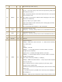
Functional Descriptions
The following figure is the block diagram of the CMOS Image Sensor. Image data
are dumped out from the Y(7:0) and UV(7:0) port. The image data format can be
either RGB, YUV or YCbCr depending on the internal register settings. The
registers are programmed via the SCCB I2C interface controlled by the external
host processor. Automatic exposure and white-balance control units are
embedded in the sensor, which can be adjusted or turned on/off via the SCCB
interface.
There are two types of operation modes: Master and Slave. In Master Mode, the
sensor are self timed generating synchronizing signals VSYNC, CHSYNC( vertical
& horizontal synchronous signals) with line by line image data on Y & UV ports.
Image data are clocked out by the PCLK, which is derived from the system clock
XVCLK1. Image data is valid only when HREF is active.
In Slave Mode, external synchronizing signals are required to be fed into the
VSYNC and CHSYNC pins. And the clock cycles required in-between are as
follows.
The pixels of the image sensor are arranged as the following table. While several
different output formats are also available as in the following table.
A. RGB Output
•
•
•
Y port output data sequence: G R G R G R ... or G G G G ...
UV port output data sequence: B G B G B G ... or B R B R ...
Array Color Filter Patter is Bayer-Pattern
B. Output Modes
•
•
16-bit Format (HREF total 292)
o Default mode:
o – 1st HREF Y channel output unstable data, UV output B11 G12 B13
G14 ....
o – 2nd HREF Y channel output G21 R22 G23 R24 ..., UV output B11
G12 B13 G14 ...
o – 3rd HREF Y channel output G21 R22 G23 R24 ..., UV output B31
G23 B33 G34 ....
o – Every line of data is output twice.
YG mode:
o – 1st HREF Y and UV output unstable data.
o – 2nd HREF Y channel output G21 G12 G23 G14 ..., UV output B11
R22 B13 R24 ...
– 3rd HREF Y is G21 G32 G23 G34 ..., UV channel is B31 R22 B33
R24 ...
o – Every line data output twice.
One line mode:
o
•
o
– 1st HREF Y channel output B11 G12 B13 G14 ...,
– 2nd HREF Y channel output G21 R22 G23 R24 ...,
– UV channel tri-state.
Format (HREF total 292)
– 1st HREF Y channel output unstable data.
– 2nd HREF Y channel output B11 G21 R22 G12 ...
– 3rd HREF Y channel output B31 G21 R22 G32 ..., etc.
– PCLK timing is double and PCLK rising edge latch data bus. UV
channel tri-state. Every line data output twice.
Nibble Mode Output Format
– Uses higher 4 bits of Y port (Y[7:4]) as output port.
– Supports YCrCb/RGB data, CCIR601/CCIR656 timing, Color/B&W.
o
– Output sequence: High order 4 bits followed by lower order 4 bits
o
o
o
•
8-bit
o
o
o
o
•
4-bit
o
Y0h Y0l Y1h Y1l ...
U0h U0l V0h V0l ...
•
For B/W or one-line RGB raw data, the output data clock speed is doubled.
For color YUV, output clock is four times that of the 16-bit output data. In
color mode, sensor must be set to 8-bit mode, and the nibble timing, clock
divided by 2.
o – Output sequence: U0h U0l Y0h Y0l V0h V0l Y1h Y1l ...
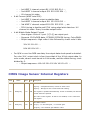
CMOS Image Sensor Internal Registers
Addr
Name
Rst
R/W Description
AGC Gain Control
GC[7:6] - unimplemented bit, returns ‘X’ when read.
GC[5:0] – Storage for the current AGC Gain setting.
00
Gain[6:0]
00
RW
This register is updated automatically. If AGC is enabled, the internal
control stores the optimal
gain value in this register. IF AGC is not enabled, a “00” is stored in
this register.
Blue Gain Control
01
Blue[7:0]
80
RW
BLU[7] – “0” decrease gain, “1” increase gain.
BLU[6:0] – blue channel gain balance value.
Red Gain Control
02
Red[7:0]
80
RW
RED[7] – “0” decrease gain, “1” increase gain.
RED[6:0] – red channel balance value.
03
Sat
80
RW
05
Cnt
48
RW
06
Brt
80
RW
Saturation Control
SAT[7:0] – saturation adjustment. “FFh”- highest, “00h”-lowest
Contrast Control
CTR[7:0] – contrast adjustment. “FFh”-highest, “00h”-lowest
Brightness Control
BRT[7:0] – brightness adjustment. “FFh”-highest,“00h”-lowest
Sharpness Control
07
Sharpness
C6
RW
SHP[7:4] – Threshold of sharpness. Range: 0~80mV, Step: 5 mV
SHP[3:0] – Sharpness control. Range: 0 ~ 8x, Step: 0.5x
White Balance Background: Blue Channel
ABLU[7:6] - Reserved
0C
AWB - Blue
20
R/W
ABLU[5] - Sign bit.
“0” - decrease background blue component
“1” - increase background blue component
ABLU[4:0] - White balance blue ratio adjustment
White Balance Background: Red Channel
ARED[7:6] - Reserved
0D
AWB - Red
20
R/W
ARED[5] - Sign bit.
“0” - decrease background red component
“1” - increase background red component
ABLU[4:0] - White balance red ratio adjustment
Common Control R
0E
COMR
0D
RW
COMR[7] - Analog signal 2x gain control bit. “1” - Additional 2x gain,
“0” - normal
COMR[6:0] - Reserved
Common Control S
COMS[7:6] - Reserved
COMS[5:4] - Black expanding level
0F
COMS
05
RW
“00” - 1.2V, “01” - 1.26V, “10” - 1.3V, “11” - 1.4V
COMS[3:2] - Set high threshold level
“00” - 1.9V, “01” - 2.0V, “10” - 2.1V, “11” - 2.2V
COMS[1:0] - Set low threshold level
“00” - 1.3V, “01” - 1.45V, “10” - 1.5V, “11” - 1.6V
10
AEC
9A
R
Automatic Exposure Control
AEC[7:0] - Set exposure time
Interlaced: Tex = Tline x AEC[7:0]
Progressive: Tex = Tline x AEC[7:0] x 2
Clock Rate Control
CLKRC[7:5] – Sync output polarity selection
“00” - HSYNC=Neg, CHSYNC=Neg, VSYNC=Pos
11
CLKRC
00
R
“01” - HSYNC=Neg, CHSYNC=Neg, VSYNC=Neg
“10” - HSYNC=Pos, CHSYNC=Neg, VSYNC=Pos
“11” - HSYNC=Pos, CHSYNC=Pos, VSYNC=Pos
CLKRC[5:0] – Clock prescaler
CLK = (CLK_main / ((CLKRC[5:0] + 1) x 2)) / 2
Common Control A
COMA[7] - SRST, “1” initiates soft reset. Initiate soft reset. All
registers are set to default values
and chip is reset to known state and resumes normal operation. This
bit is automatically
cleared after reset.
12
COMA
24
RW
COMA[6] - MIRR, “1” selects mirror image
COMA[5] - VSFR, “1” enables AGC,
COMA[4] - Digital output format, “1” selects 8-bit: Y U Y V Y U Y V
COMA[3] - Select video data output: “1” - select RGB, “0” - select
YCrCb
COMA[2] - Auto White Balance “1” - Enable AWB, “0” - Disable AWB
COMA[1] - Color Bar Test Pattern: “1” - Enable color bar test pattern
COMA[0] - reserved
Common Control B
COMB[7] - reserved
COMB[6] - reserved
COMB[5] - Select data format. “1” - Select 8-bit format, Y/CrCb and
RGB is multiplexed to 8-bit
13
COMB
01
RW
Y bus, UV bus is tri-stated, “0” - Select 16-bit format
COMB[4] - “1” - enable digital output in CCIR656 format
COMB[3] - CHSYNC output: “1” - Horizontal sync, “0” - composite
sync
COMB[2] - “1” - Tristate Y and UV busses. “0” - enable both busses
COMB[1] - “1” - Initiate single frame transfer
COMB[0] - “1” - Enable auto adjust mode
14
COMC
00
RW
Common Control C
COMC[7] - reserved
COMC[6] - reserved
COMC[5] - QCIF digital output format selection. 1 - 176x144; 0 352x288.
COMC[4] - Field/Frame vertical sync output in VSYNC port selection: 1
- frame sync, only
ODD field vertical sync; 0 - field vertical sync, effect in Interlaced
mode
COMC[3] - HREF polarity selection: 0 - HREF positive effective, 1 HREF negative.
COMC[2] - gamma selection: 1 - RGB Gamma on ; 0 - gamma is 1.
COMC[1] - reserved
COMC[0] - reserved
Common Control D
COMD[7] - reserved bit.
COMD[6] - PCLK polarity selection. “0” output data at PCLK falling
edge and data bus
will be stable at PCLK rising edge; “1” rising edge output data and
stable at PCLK falling
15
COMD
01
RW
edge. When work as CCIR656 format, COMB4=1, this bit is disable
and should
use PCLK rising edge latch data bus.
COMD[5:1] - reserved bit.
COMD[0] - U V digital output sequence exchange control. 1 - UV UV ...
for 16-bit, U Y V Y ...
for 8-bit; 0 - V U V U ... for 16Bit and V Y U Y ... for 8 Bit.
Field Slot Division
FSD[7:2] - Field interval selection. Odd Even mode defined by FD[1:0]
000000 - disable digital data output, only output black reference level.
000001 - divide to 2 slots, HREF is active one in every 2 field/frame
000010 - divide to 4 slots, HREF is active one in every 4 field/frame
000100 - divide to 8 slots, HREF is active one in every 8 field/frame
16
FSD
03
RW
001000 - divide to 16 slots, HREF is active one in every16 field/frame
010000 - divide to 32 slots, HREF is active one in every 32 field/frame
100000 - divide to 64 slots, HREF is active one in every 64field/frame
FSD[1:0]- field mode selection. Each frame consists of two fields: Odd
& Even, these bits
defines the assertion of HREF in relation to the two fields.
00 - OFF mode; HREF is not asserted in both fields, one exception is
the single frame
transfer operation (see the description for the register 13)
01 - ODD mode; HREF is asserted in odd field only.
10 - EVEN mode; HREF is asserted in even field only.
11 - FRAME mode; HREF is asserted in both odd field and even field.
FD[7:2] useless.
Horizontal HREF Start
HS[7:0] - selects the starting point of HREF window, each LSB
represents two pixels for CIF
resolution mode, one pixels for QCIF resolution mode, this value is set
based on an internal
17
HREFST
38
RW
column counter, the default value corresponds to 352 horizontal
window. Maximum window
size is 356. see window description below. HS[7:0] programmable
range is [38]- [EB], and
should less than HE[7:0]. HS[7:0] should be programmable to value
larger than or equal to
[38]. Value larger than [EC] is invalid. See window description below.
Horizontal HREF End
HE[7:0] - selects the ending point of HREF window, each LSB
represents two pixels for full
resolution and one pixels for QCIF resolution, this value is set based
on an internal column
18
HREFEND
EA
RW
counter, the default value corresponds to the last available pixel. The
HE[7:0]
programmable range is [39] - [EC]. HE[7:0] should be larger than
HS[7:0] and less than or
equal to [EC]. Value larger than [EC] is invalid. See window
description below.
Vertical Line Start
VS[7:0] - selects the starting row of vertical window, in full resolution
19
VSTRT
03
RW
mode, each LSB
represents 1 scan line in one frame. see window description below.
Min. is [03], max. is [93]
and should less than VE[7:0].
Vertical Line End
VE[7:0]- selects the ending row of vertical window, in full resolution
20
VEND
92
RW
mode, each LSB
represents 1 scan line in one frame, see window description below.
Min. is [04], max. is [94]
and should larger than VS[7:0].
Pixel Shift
PS[7:0] - to provide a way to fine tune the output timing of the pixel
data relative to that of
HREF, it physically shifts the video data output time late in unit of pixel
clock as shown in the
1B
PSHFT
00
RW
figure below. This function is different from changing the size of the
window as is defined by
HS[7:0] & HE[7:0] in register 17&18.
Higher than default number shifts the pixel in delay(right) direction,
the highest number is
“FF”. so maximum shift number is: Late: 256 pixels.
Manufacture ID Byte: High
1C
MIDH
7F
R
1D
MIDL
A2
R
1E
Rsvrd1E
C4
R
reserved
1F
Rsvrd1F
04
R
reserved
MIDH[7:0] - read only, always returns “7F” as manufacturer’s ID no.
Manufacture ID Byte: Low
MIDL[7:0] - read only, always returns “A2” as manufacturer’s ID no.
Common Control E
COME[7] - HREF pixel number selection. “1” - HREF include 704 PCLK,
every data output
twice.
COME[6] - reserved.
COME[5] - “1” First stage aperture correction enable. Correction
strength will be decided by
register [07]. “0” disable first stage aperture correction.
COME[4] - “1” Second stage aperture correction enable. Correction
20
COME
00
RW
strength and threshold
value will be decided by COMF[7] ~ COMF[4].
COME[3] - AWB smart mode enable. 1 - Drop out pixel when compare
pixel red, blue and
green component level to change register [01] and [02], which
luminance level is higher than
presetting level and lower than presetting level, this two level is set by
register [0F].
0 - calculate all pixels to get AWB result. Valid only when COMB[0]=1
and COMA[2]=1
COME[2] - AWB stop when field/frame image average luminance level
is lower than a
presetting level enable. 1 - enable stop AWB when image luminance
level is low. 0 - AWB is
independent with field/frame luminance level. Valid only when
COMB0=1 and COMA[2]=1.
Average compare level is set by GAM[7:5].
COME[1] - AWB fast/slow mode selection. “1” - AWB is always fast
mode, that is register [01]
and [02] is changed every field/frame. “0” AWB is slow mode, [01]
and [02] change every 16/
64 field/frame decided by COMK[1]. When AWB enable, COMA[2]=1,
AWB is working as
fast mode at first 1024 field/frame, than as slow mode later.
COME[0] - Digital output driver capability increase selection: “1”
Double digital output driver
current; “0” low output driver current status.
Y Channel Offset Adjustment
YOFF[7] - Offset adjustment direction 0 - Add Y[6:0]; 1 -Substrate
Y[6:0].
YOFF[6:0] -Y channel digital output offset adjustment. Range:
+127mV ~ -127mV. If
COMG[2]=0, this register will be updated by internal auto A/D BLC
circuit, and write a value
21
YOFF
80
RW
to this register with SCCB has no effect. If COMG[2]=1, Y channel
offset adjustment will use
the register stored value which can be changed by SCCB. If
COMF[1]=0, this register has
no
adjustment effect to A/D output data. If output RGB raw data, this
register will adjust R/G/Bdata.
U Channel Offset Adjustment
UOFF[7]: - Offset adjustment direction: 0 - Add U[6:0]; 1 -Substrate
U[6:0].
22
UOFF
80
RW
UOFF[6:0] - U channel digital output offset adjustment. Range:
+128mV ~ -128mV. If
COMG[2]=0, this register will be updated by internal auto A/D BLC
circuit, and write a value
to this register with SCCB has no effect. If COMG[2]=1, U channel
offset adjustment will use
the register stored value which can be changed by SCCB. If
COMF[1]=1, this register has
no effect to A/D output data. If output RGB raw data, this register will
adjust R/G/B data.
Reference Control
REFC[7:6] - Select different crystal circuit power level (11 =
23
REFC
04
RW
minimum).
REFC[5:4] - reserved
REFC[3:0]: Reference Voltage range selection. 2.5V - 3.5V and step is
0.0625V.
Automatic Exposure Control: Bright Pixel Ratio Adjustment
AEW[7:0] - Used as calculate bright pixel ratio. AEC algorithm is count
whole field/
frame bright pixel (its luminance level is higher than a fixed level) and
black pixel (its
luminance level is lower than a fixed level) number. When
bright/black pixel ratio is same as
the ratio defined by register [25] and [26], image stable. This register
24
AEW
33
RW
is used to define bright
pixel ratio, default is 25%, each LSB represent step: 1.3% Change
range is: [01] ~ [CA];
Increase AEW[7:0] will increase bright pixel ratio. For same light
condition, the image
brightness will increase if AEW[7:0] increase.
Note: AEW[7:0] must combine with register [26] AEB[7:0].
The relation must be as
follows: AEW[7:0] + AEB[7:0] > [CA].
Automatic Exposure Control: Black Pixel Ration Adjustment
AEB[7:0] - used as calculate black pixel ratio. AEC algorithm is count
whole field/
frame bright pixel (its luminance level is higher than a fixed level) and
black pixel (its
25
AEB
97
RW
luminance level is lower than a fixed level) number. When
bright/black pixel ratio is same as
the ratio defined by register [25] and [26], image stable. This register
is used to define black
pixel ratio, default is 75%, each LSB represent step: 1.3%; Change
range is: [01] ~ [CA];
Increase AEB[7:0] will increase black pixel ratio. For same light
condition, the image
brightness will decrease if AEB[7:0] increase.
Note: AEB[7:0] must be combined with register [25] AEW[7:0].
The relation must be as follows: EW[7:0] + AEB[7:0] > [CA].
Common Control F
COMF[7:6] - Second aperture correction threshold selection.
[00] - Difference of neighbor pixel luminance is larger than 8 mV,
correction on.
[01] - 16 mV.
[10] - 32 mV.
[11] - 64 mV.
COMF[5:4] - Second aperture correction strength selection.
[00] and [01] - Strength is 50% of difference of neighbor pixel
26
COMF
B0
RW
luminance.
[10] - 100%.
[11] - 200%.
COMF[3] - UV BLC swap. “1” swap; “0” no swap.
COMF[2] - Digital data MSB/LSB swap. “1” LSB->Bit7, MSB->Bit0; “0”
normal.
COMF[1] - “1” A/D Black level calibration enable. “0” Disable A/D BLC.
COMF[0] - “1” Output first 4 line black level before valid data output.
HREF number will
increase 4 relatively. “0” no black level output.
Common Control G
COMG[7] - reserved
COMG[6] - reserved.
COMG[5] - Select CKOUT pin output V flag. 1 - CKOUT output V flag
signal. CKOUT=1,
means related UV channel output V component (or Red component),
CKOUT=0 pointed to
27
COMG
A0
RW
U component (or Blue component). 0 - CKOUT output buffered XCLK2
COMG[4] - reserved.
COMG[3] - reserved
COMG[2] - “1” A/D offset adjustment manually mode enable: 1 - A/D
data will be add/substrate a value defined by register [21] and [22],
which content is written by SCCB. 0 - A/D data will be added/substrate
a value defined by register [21] and [22], which is updated by internal
circuit.
COMG[1] - Digital output full range selection. output data value range
is [10] - [F0], if
COMG[1] -1, range change to [01] - [FE] with signal overshoot and
undershoot level.
COMG[0] - reserved.
Common Control H
COMH[7]: - “1” selects One-Line RGB raw data output format, “0”
selects normal two-line RGB raw data output, effective only in
Progressive Scan mode.
COMH[6]: - “1” enable Black/White mode. When working as BW
camera, its vertical resolution will be higher than color mode. At this
mode, can’t set working at 8 bit output mode. output data YUV/RGB
from Y port. UV port will be tri-state. COMB[5]
and COMB[4] will be set to “0”. “0” normal color mode.
COMH[5]: - reserved.
COMH[4]: - Freeze AEC/AGC value, effective only when COMB0=1.
“1” - register [00] and [10] will not be updated and hold latest value.
“0” - AEC/AGC normal working status.
28
COMH
01
RW
COMH[3]: - AGC disable. 1 - when COMB[0]=1 and COMA[5]=1,
internal circuit will not update register [00], register [00] will kept
latest updated value before COMH[3]=1.;
0 – when COMB0=1 and
COMA[5]=1, register [00] will be updated by internal algorithm.
COMH[2]: - RGB raw data output YG format: 1 - Y channel G, UV
channel B R; 0 - Y channel:
G R G R..., UV channel B G B G....
COMH[1]: - Gain control bit. “1” Double PreAmp gain to 12dB. “0”
PreAmp gain is 6dB.
COMH[0]: - High gain mode. “1” - AGC maximum gain is 24dB. AGC
step is 1/8. “0” AGE
maximum gain is 18dB, AGC step is 1/16. Only effective when
COMB[0]=1, COMA[5]=1 and
COMH[3]=0.
Common Control I
COMI[7]: - AEC disable. “1” If COMB[0]=1, AEC stop and register [10]
value will be held at last
29
COMI
00
RW
AEC value and not be updated by internal circuit. “0” - if COMB[0]=1,
register [10] value will
be updated by internal circuit
COMI[6]: - Slave mode selection. “1” slave mode, use external Sync
and Vsync; “0” master
mode
COMI[5]: - reserved
COMI[4]: - reserved
COMI[3]: - Central 1/4 image area rather whole image used to
calculate AEC/AGC. “0” use
whole image area to calculate AEC/AGC.
COMI[2]: - reserved
COMI[1:0] - Version flag. For Version A, value is [00], these two bits
can only be read.
Frame Rate Adjust High
FRARH[7] - Frame Rate adjustment enable bit. “1” Enable.
FRARH[6] - reserved
FRARH[5] - Highest 1bit of frame rate adjust control byte. see
explanation below.
FRARH[4] - reserved
2A
FRARH
84
RW
FRARH[3] - Y channel brightness adjustment enable. When
COMF[2]=1 active.
FRARH[2] - reserved
FRARH[1] - “1” When in Frame exposure mode, only One frame data
output.
FRARH[0] - reserved
Frame Rate Adjust Low
FRARL[7:0] - Lowest 8 bit of frame rate adjust control byte. Frame
rate adjustment resolution
2B
FRARL
5E
RW
is 0.21%. Control byte is 10 bit. Every LSB equal decrease frame rate
0.21%. Range is
0.21% - 109%. IF frame rate adjustment enable, COME7 must set to
“0”.
2C
Rsvd2C
88
RW
reserved
Common Control J
COMJ[7:5] - reserved
COMJ[4] - Enable auto black expanding mode.
2D
COMJ
03
RW
COMJ[3] - “1” = White Balance update when AGC/AEC stable. “0” =
White Balance register
update independent with AEC/AGC.
COMJ[2] - Band filter enable. After adjust frame rate to match indoor
light frequency, this bit
enable a different exposure algorithm to cut light band induced by
fluorescent light.
COMJ[1] - reserved
COMJ[0] - A/D U and V BLC separate mode. “1” = U and V offset
cancelled by different
register. “0” = U V offset cancelled by one common register [2E].
V Channel Offset Adjustment
VCOFF[7]: Offset adjustment direction: “0” = Add V[6:0]; “1” =
Substrate V[6:0].
VCOFF[6:0] - V channel digital output offset adjustment. Range:
+128mV ~ -128mV. If
COMG[2]=0, this register will be updated by internal auto A/D BLC
2E
VCOFF
80
RW
circuit, and write a value
to this register with SCCB has no effect. If COMG[2] =1, V channel
offset adjustment will use
the register stored value which can be changed by SCCB. If COMF[1]
=1, this register has
no effect to A/D output data. If output RGB raw data, this register will
adjust R/G/B data.
2F-32 Rsvd2F-Rsvd32
xx
-
Reserved
Color Processing Parameter Control
CPP[7:6] - reserved
33
CPP
00
RW
CPP[5] - Luminance gamma on/off. “1” - luminance gamma on; “0” luminance gamma is 1.
CPP[4:0] - reserved
Bias Adjustment
BIAS[7:6] - A/D reference level adjustment. [00] - 110% internal full
34
BIAS
A2
RW signal range; [01] - 120%,
[10] - 130%, [11] - 140%.
BIAS[5:0] - reserved
35
Rsvd35
80
RW
reserved
36
Rsvd36
48
RW
reserved
37
Rsvd37
41
RW
reserved
Common Control K
38
COMK
81
RW
COMK[7] - HREF edge latched by PCLK falling edge (When COMD[6] =
0). “0” HREF edge is
10 ns after PCLK rising edge.
COMK[6] - Output port drive current additional 2x control bit.
COMK[5] - reserved.
COMK[4] - ZV port Vertical timing selection. “1” VSYNC output ZV port
vertical sync signal.
“0” = normal TV vertical sync signal.
COMK[3] - Quick stable mode when camera mode change. After
relative control bit set, the
first VS will be the stable image with suitable AEC/AWB setting. “0” slow mode, after mode
change need more field/frame to get stable AEC/AWB setting image.
COMK[2] - reserved
COMK[1] - AWB stable time selection when in slow mode. “1” - 4 times
less time needed to get
stable AWB setting when in slow AWB mode.
COMK[0] -reserved.
Common Control L
COML[7] - reserved
COML[6] - PCLK output timing selection. 1 -- PCLK valid only when
HREF is high; 0 -- PCLK is
free running.
COML[5] - Vertical sync selection, 1 -- Same period between 1st HREF
and VS falling edge in
two field; 0 - Different timing period between 1st HREF and VS falling
39
COML
00
RW
edge
COML[4] - “1” select CHSYNC output from HREF port. “0” normal
COML[3] - “1” select HREF output from CHSYNC port. “0” normal
COML[2] - Tristate all control signal output (FODD, CHSYNC, HREF,
PCLK)
COML[1] - Highest 1 bit of horizontal sync starting position, combined
with register [3A]
COML[0] - Highest 1 bit of horizontal sync ending position, combined
with register [3B]
Horizontal Sync Start Position
HSST[7:0] - lower 8 bit of horizontal sync starting position, combined
3A
HSST
0F
RW
with register bit of
COML[1], total 9 bit control. range: [00] -- [FF]. HSEND[8:0] must
less than HSST[8:0]
3B
HSEND
3C
RW
Horizontal Sync End Position
HEND[7:0] - lower 8 bit of horizontal sync ending position, combined
with register bit of
COML[0], total 9 bit control. range: [00] -- [FF]. HSEND[8:0] must be
larger than HSST[8:0]
Common Control M
COMM[7:5] - Select minimum AEC number if Banding filter enable.
[000] -- 1 field, [001] -- 1/2;
[010] -- 1/4; [011] -- 1/8; [100] -- 1/16; [101]~[111] -- 1/32;
3C
COMM
21
RW
COMM[4] - AEC/AGC change mode selection
COMM[3] - AEC/AGC change mode selection
COMM[2] - AEC/AGC change fastest mode
COMM[1] - AEC/AGC change fast mode
COMM[0] - AEC/AGC change slowest mode
Common Control N
COMN[7] - Enable one frame drop when AEC change to keep data
valid when Banding filter
3D
COMN
08
RW
mode enable.
COMN[6:4] - reserved
COMN[3] - Enable 50 Hz PAL video timing, so VTO analog signal can
be displayed on TV
COMN[2:0] - reserved
Common Control O
COMO[7] - Input main clock divided by 2 or 4 selection. 1 -- 2; 0 -- 4
COMO[6:5] - reserved
3E
COMO
80
RW
COMO[4] - Select 4 bit nibble mode output
COMO[3] - reserved
COMO[2] - Enable Minimum exposure time is 4 line. Default is 1 line
COMO[1] - reserved
COMO[0] - reserved
Common Control P
COMP[7] - reserved
COMP[6] - Output main clock output from FODD port
COMP[5] - reserved
3F
COMP
02
RW
COMP[4] - Software whole chip power down enable, can be waked up
by disable this bit
COMP[3:2] - reserved
COMP[1] - CCIR656 output control
COMP[0] - Reset internal timing circuit without reset AEC/AGC/AWB
value
40
Rsvd40 Rsvd4C
XX
-
reserved
YUV Matrix Control (Main)
YMXA[7:5] - reserved
YMXA[4:3] - YUV/YCrCB selection:
4D
YMXA
02
RW
[00] U = u, V = v
[01] U = 0.938u, V = 0.838v
[10] U = 0.563u, V = 0.714v
[11] U = 0.5u, V = 0.877v
YMXA[2:0] - Reserved
AEC/AGC Reference Level
ARL[7:5] - Reference Level Voltage Selection (Higher voltage =
brighter final stable image)
[000] = 1.3v
[001] = 1.5v
4E
ARL
A0
RW
[010] = 1.6v
[011] = 1.7v
[100] = 1.8v
[101] = 1.9v
[110] = 2.0v
[111] = 2.1v
ARL[4:0] - Reserved
YUV Matrix Control (Secondary)
YMXB[7:6] - Y channel delay selection: 0 ~ 3 tp
YMXB[5:4] - UV delay selection: 0 ~ 6 tp
4F
YMXB
00
RW
YMXB[3:2] - Select UV average mode. [00] & [10]: U0/V0 (no delay);
[01] -- 3 point average;
[11] -- 5 point average mode
YMXB[1:0] - Color killer control:
[00]:2.4v;[01]:2.6v;[10]:2.8v;[11]:3.0v
50
Rsvd50 Rsvd53
XX
-
reserved
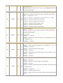
Schematic of the Module
J59
J60
FPGA CMOS FPGA CMOS
FPGA CMOS FPGA CMOS
Pin
Pin
Pin
Pin
Pin
Pin
Pin
Pin
5V
cv5v
GK2
cck2
3V
cv3v
3V
cv3v
V6
cy0
AB1
cy1
AB2
chsyn
AA3
chref
U7
cy2
AA2
cy3
AA4
cvsyn
W4
cpckp
Y5
cy4
AA5
cy5
GND
cgnd
GND
cgnd
W5
cy6
W6
cy7
Y6
cuv0
AB6
cuv1
Y4
cuv2
V7
cuv3
U8
cuv4
W7
cuv5
AA7
cuv6
Y7
cuv7
GK0X
cck0
GND
cgnd
J62
J64
FPGA CMOS FPGA CMOS
Pin
Pin
Pin
Pin
5V
cv5v
GK1Y
cck1
W9
csar0
W8
csar1
AA8
csar2
AB8
csar3
U9
csar4
Y9
csar5
V8
csar6
V9
csar7
AA9
csc0
AB9
csc1
Pin
Pin
Pin
Pin
U10
csc2
V10
csc3
3V
cv3v
3V
cv3v
W10
cski0
Y10
cski1
AA10
csip0
AB10
csip1
U11
cski2
Y11
cski3
AA11
cfrex
U12
cfodd
GK4
cck3
GND
cgnd
GND
cgnd
GND
cgnd
FPGA CMOS FPGA CMOS
Pin
Type Function
cy[7:0]
out
CMOS image sensor Y/ S20 dip switch output
cuv[7:0]
out
CMOS image sensor UY/ S15 dip switch output
csar[7:0]
in
7-segment anode input
csc[3:0]
in
7-segment cathode/ 4x4 key pad scan input
cski[3:0] inout 4x4 key pad scan ouput/ PS2 kbd-mouse pins
Jumper Pin-Outs
J61 Pin-outs
cmult
v5v
crst
v5v
cagc
v5v
cpwdn
v5v
csbb
v5v
J61
Pin
Type Function
cmult
in
Multi-CMOS image sensors enable
crst
in
CMOS image sensor reset
cagc
in
CMOS image sensor auto-gain-control enable
cpwdn
in
CMOS image sensor power down
csbb
in
CMOS image sensor host serial bus control enable
J61 Default Setting
J66 Pin-outs
xclk2
xtal2
xclk1
xtal1
cpckp
xclk1
cck0
cpckp
xclk1
cck1
cpckp
xclk1
cck2
cpckp
xclk1
cck3
J66
Pin
Type 功能說明
xclk[2:1]
in
cpckp
out
CMOS pixel clock output
cck[3:0]
out
Global clocks from/to main board
cck[3:0]
out
Global clocks from/to main board
J66 Default Setting
CMOS image sensor clock input
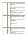
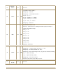
Testing Example
Host
Interface
VGA
Timing
Generator
VGA
Display
VGA
Data
I2C
PORT
IMAGE
SENSOR
Timing
Generator
SENSOR
TSTCAMC
IMAGE
Host:
PC IDS
Forth
Or
AVR uP
IMAGE
SENSOR
Data
1. Host (PC IDS Forth or AVR processor) initializes the registers (detailed
commands in the following paragraph) of the IMAGE SENSOR via the I2C
PORT, and enables the IMAGE SENSOR Timing Generator.
2. After the IMAGE SENSOR is properly configured, it then sends image data
according to the synchronous signals from the IMAGE SENSOR Timing
Generator.
3. VGA Timing Generator that is synchronous with the IMAGE SENSOR Timing
Generator, enables the VGA Display and with display data conveyed from the
IMAGE SENSOR.
TstCamc.v
module tstcamb
(
mclk,
haddr,alxp,hwr,hrd,
csda,csck,
cyp,cuvp,
cfoddp,cfrexp,cfrefp,
tout,
vhsyp,vvsyp,
chsynp,cvsynp,
vblnp,vlcsp1,
vgp,vbp,vrp
);
input mclk; // System clock
input hwr,hrd; // host read/write
input[2:0] haddr; // host address
inout[7:0] alxp; // host data
inout csda,csck; // CMOS Image Sensor(CIS) I2C Port
input[7:0] cyp,cuvp; // CIS Video Data
input cfoddp,cfrexp,cfrefp; // CIS Synchronizing signals
output chsynp,cvsynp; // CIS Synchronizing signals
output tout; // Test output for reserving unused inputs
output vhsyp,vvsyp; // VGA synchronizing signals
output vblnp,vlcsp1; // VGA synchronous blanking signals
output[7:0] vgp,vbp,vrp; // VGA Video Data
reg hwrs,hwrss,hrds,hrdss;
reg[7:0] vldp;
reg csdas,cscks;
reg[7:0] hdto,breg,rreg,greg;
wire hwrp;
reg[1:0] brf;
reg[9:0] hcnt;
reg hov,hsyns,hsyne,chsyns,chsyne;
reg hsyn,chsyn;
reg[9:0] vcnt;
reg vov,vsyns,vsyne,cvsyns,cvsyne;
reg vsyn;
reg cvsyn;
always @(posedge mclk) // Bayer’s format reconstruct counter
begin
if(~cfrefp) brf<=0; else brf<=brf+1;
end
always @(posedge mclk) // Bayer’s format reconstruct R/G/B latch
begin
if(~brf[1]) breg<=cuvp;
if(brf[1]) rreg<=cuvp;
greg<=cyp;
end
always @(posedge mclk) // Host Signal synchronization
begin
hwrs<=hwr; hwrss<=hwrs;
hrds<=hrd; hrdss<=hrds;
end
assign hwrp=hwrs&~hwrss; // Synchronous Host write pulse
always @(posedge mclk) // Host Interface Register write
begin
if(hwrp)
begin
if(haddr==0) csdas<=alxp[0]; // CIS I2C data
if(haddr==1) cscks<=alxp[0]; // CIS I2C clock
if(haddr==4) vldp<=alxp; // CIS sync signals Enable bit vldp[0]
end
end
always @(haddr or csda or csck) // Host Interface Read
begin
case(haddr)
0 : begin hdto={7'b0000000,csda}; end
1 : begin hdto={7'b0000000,csck}; end
default : hdto=8'b00000000;
endcase
end
assign alxp=hrd?hdto:8'bzzzzzzzz;
assign csda=csdas?1'bz:1'b0; // I2C data Open Drain
assign csck=cscks?1'bz:1'b0; // I2C clock Open Drain
assign tout=(&cuvp)&cfrexp&cfoddp; // reserving unused CIS inputs
assign vhsyp=hsyn;
assign vvsyp=vsyn;
assign vgp=cfrefp?greg:8'h00;
assign vbp=cfrefp?breg:8'h00;
assign vrp=cfrefp?rreg:8'h00;
assign vblnp=1'b1;
assign vlcsp1=1'b1;
assign chsynp=vldp[0]?chsyn:1'bz;
assign cvsynp=vldp[0]?cvsyn:1'bz;
always @(posedge mclk) // Horizontal Counter
begin
if(hov) hcnt<=0;
else hcnt<=hcnt+1;
end
always @(posedge mclk)
begin
hov<=(hcnt==795);
hsyns<=(hcnt==652);
hsyne<=(hcnt==747);
chsyns<=(hcnt==452);
chsyne<=(hcnt==547);
end
always @(posedge mclk) // VGA HSYNC
begin
case(hsyn)
1'b0 : if(hsyns) hsyn<=1'b1;
1'b1 : if(hsyne) hsyn<=1'b0;
endcase
end
always @(posedge mclk) // CIS HSYNC
begin
case(chsyn)
1'b0 : if(chsyns) chsyn<=1'b1;
1'b1 : if(chsyne) chsyn<=1'b0;
endcase
end
always @(posedge mclk)
// Vertical Counter
begin
if(hsyns)
begin
if(vov) vcnt<=0;
else vcnt<=vcnt+1;
end
end
always @(posedge mclk)
begin
vov<=(vcnt==522);
vsyns<=(vcnt==390);
vsyne<=(vcnt==392);
cvsyns<=(vcnt==490);
cvsyne<=(hcnt==200);
end
always @(posedge mclk) // VGA VSYNC
begin
case(vsyn)
1'b0 : if(vsyns) vsyn<=1'b1;
1'b1 : if(vsyne) vsyn<=1'b0;
endcase
end
always @(posedge mclk) // CIS VSYNC
begin
case(cvsyn)
1'b0 : if(cvsyns) cvsyn<=1'b1;
1'b1 : if(cvsyne) cvsyn<=1'b0;
endcase
end
endmodule
Pin Assignment
PORT
CMOS
FPGA
PORT
ADDA
FPGA
Name
Name
Pin
Name
Name
Pin
frq0
cy0
V6
scko
adackp
B8
frq1
cy1
AB1
sdo
adasdp
D8
frq2
cy2
U7
scso
adacs
D10
frq3
cy3
AA2
sldo
adald
C9
frq4
cy4
Y5
sclo
adacl
A9
frq5
cy5
AA5
cnvo
aadcv
E11
frq6
cy6
W5
cso
aadcs
F11
frq7
cy7
W6
rdo
aadrd
D11
frq8
cuv0
Y6
ado0
aada0
A11
frq9
cuv1
AB6
ado1
aada1
B12
frq10
cuv2
Y4
ado2
aada2
A12
frq11
cuv3
V7
dti0
aadd0
B11
aai0
cuv4
U8
dti1
aadd1
G11
aai1
cuv5
W7
dti2
aadd2
C10
nrst
cuv7
AA7
dti3
aadd3
E10
dti4
aadd4
B9
dti5
aadd5
D9
dti6
aadd6
C8
dti7
aadd7
F9
eoci
aadec
A10
Commands of IDS Forth:
1. The Forth word that executes the IMAGE SENSOR Initialization is as the
following: (remarks insides the parenthesis)
: TST1k4 [ decimal ] 25000 ckaf 25000 ckbf 25000 ckcf ( Set clock rate in decimal 25MHz )
[ hex ] " tstcamc" loadconf
( Back to Hex mode; Load FPGA Configuration )
2 4001 hpmwr
( Enable Host Port )
0 1c iicwr iicrd . 40 29 iicwr ( iicwr: writes I2C command (Data->Addr): (0-> 1C),(40-> 29) )
1 4 tttwr 5 28 iicwr 86 2a iicwr 28 12 iicwr ( tttwr : Host Port Write (Data->Addr) (1->4), that )
40 1 iicwr 60 2 iicwr ff 3 iicwr ;
( enables the IMAGE SENSOR Timing Generator )
2. The System Clock is set to 25MHz.
3. 2 4001 hpmwr enables the Host Port
4. iicwr is the words of I2C write in the format of: ( Data Addr iicwr )
5. iicrd is the word of I2C read in the format of: ( 0 Addr iicwr iicrd ), that always
proceeded by a iicwr.
6. tttwr initiates a Host Memory Write cycle, in format of: ( Data Addr tttwr ).
7. 1 4 tttwr : writes data 1 to the address 4, which is the enable bits of IMAGE
SENSOR Timing Generator.
8. All the iicwr commands write data to the registers of the IMAGE SENSOR, ex.,
40 29 iicwr writes 40(hex) to the register 29(hex) of the IMAGE SENSOR
9. Refer to the Register Table of the Image Sensor in the previous paragraphs.
For example: 40 1 iicwr sets the blue gain of the SENSOR; 60 2 iicwr sets the
red gain if the SENSOR.
Test Procedure
Host IDS Forth
sends Commands
via this cable
Timing Generators
of IMAGE SENSOR &
VGA Display
Host Initialize
the IMAGE SENSOR
via this I2C Port
IMAGE SENSOR Data is
conveyed to the VGA
Display Port
1.
2.
3.
4.
Please refer to the Testing Procedure of IMAGE SENSOR in Chapter 1.
Set correct jumpers. And connect the VGA Cable.
In IDS, set correct Configuration file directory.
In Forth, enter “ include tst1km.fth “. Then enter “ tst1k3 “