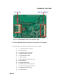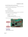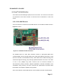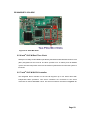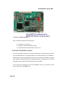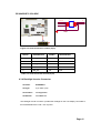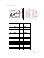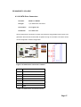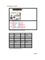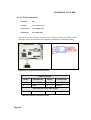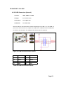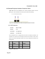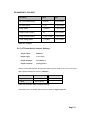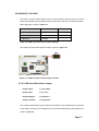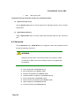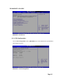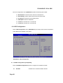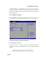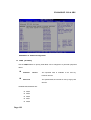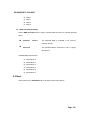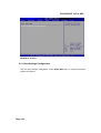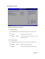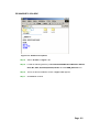
1
EX-9945GSE 5.25-A SBC
EX-9945GSE 5.25-A
5.25” SBC with 1.6 GHz Intel® Atom™ N270 Processor
LVDS/VGA/HDTV, Dual PCIe Mini, Dual PCIe GbE,
USB 2.0, SATA and RoHS Compliance
User Manual
Page 1
EX-9945GSE 5.25-A SBC
Revision
Date
Version
Changes
2008-10
1.00
Initial release
Page 2
EX-9945GSE 5.25-A SBC
Copyright
COPYRIGHT NOTICE
The information in this document is subject to change without prior notice in order to
improve reliability, design and function and does not represent a commitment on the part
of the manufacturer.
In no event will the manufacturer be liable for direct, indirect, special, incidental, or
consequential damages arising out of the use or inability to use the product or
documentation, even if advised of the possibility of such damages.
This document contains proprietary information protected by copyright. All rights are
reserved. No part of this manual may be reproduced by any mechanical, electronic, or
other means in any form without prior written permission of the manufacturer.
TRADEMARKS
All registered trademarks and product names mentioned herein are used for identification
purposes only and may be trademarks and/or registered trademarks of their respective
owners.
Page 3
EX-9945GSE 5.25-A SBC
Manual Conventions
WARNING!
Warnings appear where overlooked details may cause damage to the equipment or result
in personal injury. Warnings should be taken seriously. Warnings are easy to recognize.
The word “warning” is written as “WARNING,” both capitalized and bold and is followed by
text. The text is the warning message. A warning message is shown below:
WARNING:
This is an example of a warning message. Failure to adhere to warning
messages may result in permanent damage to the EX-9945GSE
5.25-A or personal injury to the user. Please take warning messages
seriously.
CAUTION!
Cautionary messages should also be heeded to help reduce the chance of losing data or
damaging the EX-9945GSE 5.25-A. Cautions are easy to recognize. The word “caution” is
written as “CAUTION,” both capitalized and bold and is followed. The italicized text is the
cautionary message. A caution message is shown below:
CAUTION:
This is an example of a caution message. Failure to adhere to cautions
messages may result in permanent damage to the EX-9945GSE
Page 4
EX-9945GSE 5.25-A SBC
5.25-A. Please take caution messages seriously.
NOTE:
These messages inform the reader of essential but non-critical information. These
messages should be read carefully as any directions or instructions contained therein can
help avoid making mistakes. Notes are easy to recognize. The word “note” is written as
“NOTE,” both capitalized and bold and is followed by text. The text is the cautionary
message. A note message is shown below:
NOTE:
This is an example of a note message. Notes should always be read.
Notes contain critical information about the EX-9945GSE 5.25-A.
Please take note messages seriously.
Page 5
EX-9945GSE 5.25-A SBC
Packing List
NOTE:
If any of the components listed in the checklist below are missing,
please do not proceed with the installation. Contact the TOPSCCC
reseller or vendor you purchased the EX-9945GSE 5.25-A from or
contact an TOPSCCC sales representative directly. To contact an
TOPSCCC
0H
sales
representative,
please
send
an
email
to
[email protected].
The items listed below should all be included in the EX-9945GSE 5.25-A package.
1 x EX-9945GSE 5.25-A Single Board Computer
1 x Audio cable
1 x Keyboard/Mouse Y cable
4 x RS-232 cables
2 x SATA cables
1 x USB cable
1 x VGA cable
1 x Mini Jumper Pack
1 x Utility CD
1 x QIG
Images of the above items are shown in Chapter 3.
Page 6
EX-9945GSE 5.25-A SBC
Table of Contents
1
INTRODUCTION..................................................................................................... 1
1.1 OVERVIEW.................................................................................................................. 2
1.1.1 EX-9945GSE 5.25-A Introduction ..................................................................... 2
1.2 EX-9945GSE 5.25-A OVERVIEW ............................................................................... 2
1.2.1 EX-9945GSE 5.25-A Overview Photo ............................................................... 2
1.2.2 EX-9945GSE 5.25-A Peripheral Connectors and Jumpers ............................... 4
1.2.3 Technical Specifications..................................................................................... 5
2
DETAILED SPECIFICATIONS ............................................................................. 8
2.1 DIMENSIONS ............................................................................................................... 9
2.1.1 Board Dimensions.............................................................................................. 9
2.1.2 External Interface Panel Dimensions .............................................................. 10
2.2 DATA FLOW .............................................................................................................. 10
2.3 EMBEDDED EX-9945GSE 5.25-A PROCESSOR .........................................................11
2.3.1 Overview ...........................................................................................................11
2.3.2 Features ........................................................................................................... 12
2.3.3 Front Side Bus (FSB) ....................................................................................... 13
2.4 INTEL 945GSE NORTHBRIDGE CHIPSET ................................................................... 14
2.4.1 Intel® 945GSE Overview................................................................................. 14
2.4.2 Intel® 945GSE DDR2 Controller.................................................................... 14
2.4.3 Intel® 945GSE Graphics ................................................................................. 15
2.4.3.1 Analog CRT Graphics Mode..................................................................... 16
2.4.3.2 LVDS Interface ......................................................................................... 16
2.4.3.3 TV Out Interface ....................................................................................... 16
2.5 INTEL® ICH7-M SOUTHBRIDGE CHIPSET ................................................................. 17
2.5.1 Intel® ICH7-M Overview ................................................................................. 17
2.5.1.1 Intel® ICH7-M Audio Codec ’97 Controller............................................. 17
2.5.2 Intel® ICH7-M IDE Interface........................................................................... 19
2.5.3 Intel® ICH7-M Low Pin Count (LPC) Interface .............................................. 20
2.5.4 Intel® ICH7-M PCI Interface........................................................................... 20
2.5.5 Intel® ICH7-M PCIe Bus ................................................................................. 21
Page 7
EX-9945GSE 5.25-A SBC
2.5.5.1 PCIe GbE Ethernet.................................................................................... 21
2.5.5.2 PCIe Mini Expansion Slots....................................................................... 22
2.5.6 Intel® ICH7-M Real Time Clock ...................................................................... 23
2.5.7 Intel® ICH7-M SATA Controller ...................................................................... 23
2.5.8 Intel® ICH7-M USB Controller........................................................................ 24
2.6 LPC BUS COMPONENTS ........................................................................................... 25
2.6.1 LPC Bus Overview........................................................................................... 25
2.6.2 iTE IT8718F Super I/O Chipset....................................................................... 25
2.6.2.1 Super I/O LPC Interface ........................................................................... 26
2.6.2.2 Super I/O 16C550 UARTs ........................................................................ 27
2.6.2.3 Super I/O Digital Input/Output ................................................................. 27
2.6.2.4 Super I/O Enhanced Hardware Monitor ................................................... 27
2.6.2.5 Super I/O Fan Speed Controller................................................................ 27
2.6.2.6 Super I/O Keyboard/Mouse Controller..................................................... 27
2.6.2.7 Super I/O Parallel Port .............................................................................. 28
2.7 ENVIRONMENTAL AND POWER SPECIFICATIONS ....................................................... 28
2.7.1 System Monitoring ........................................................................................... 28
2.7.2 Operating Temperature and Temperature Control........................................... 29
2.7.3 Power Consumption......................................................................................... 29
3
UNPACKING .......................................................................................................... 30
3.1 ANTI-STATIC PRECAUTIONS ...................................................................................... 31
3.2 UNPACKING .............................................................................................................. 31
3.2.1 Unpacking Precautions.................................................................................... 31
3.3 UNPACKING CHECKLIST ........................................................................................... 32
3.3.1 Package Contents............................................................................................. 32
3.3.2 Optional Items.................................................................................................. 33
4
CONNECTORS ...................................................................................................... 34
4.1 PERIPHERAL INTERFACE CONNECTORS..................................................................... 35
4.1.1 EX-9945GSE 5.25-A Layout ............................................................................ 35
4.2 PERIPHERAL INTERFACE CONNECTORS..................................................................... 36
4.2.1 External Interface Panel Connectors............................................................... 38
4.3 INTERNAL PERIPHERAL CONNECTORS ...................................................................... 38
4.3.1 AT Power Connector........................................................................................ 38
Page 8
EX-9945GSE 5.25-A SBC
4.3.2 ATX Power Supply Enable Connector ............................................................. 39
4.3.3 Audio Connector (9-pin) .................................................................................. 40
4.3.4 Backlight Inverter Connector .......................................................................... 41
4.3.5 CompactFlash® Socket.................................................................................... 42
4.3.6 CRT Connector ................................................................................................ 44
4.3.7 Digital Input/Output (DIO) Connector............................................................ 45
4.3.8 Fan Connector (+12V, 3-pin) .......................................................................... 46
4.3.9 Front Panel Connector (8-pin) ........................................................................ 47
4.3.10 IDE Connector (44-pin)................................................................................. 48
4.3.11 Infrared Interface Connector (5-pin) ............................................................. 50
4.3.12 Keyboard/Mouse Connector .......................................................................... 51
4.3.13 LVDS LCD Connector ................................................................................... 52
4.3.14 Parallel Port Connector ................................................................................ 53
4.3.15 SDVO Connector............................................................................................ 55
4.3.16 SATA Drive Connectors ................................................................................. 57
4.3.17 SATA Power Connectors ................................................................................ 58
4.3.18 Serial Port Connectors (COM 1 ~ COM 4)................................................... 58
4.3.19 COM 3 RS-422/485 Connector...................................................................... 59
4.3.20 Trusted Platform Module (TPM) Connector.................................................. 60
4.3.21 TV Out Connector .......................................................................................... 62
4.3.22 USB Connectors (Internal) ............................................................................ 63
4.4 EXTERNAL PERIPHERAL INTERFACE CONNECTOR PANEL ......................................... 64
4.4.1 LAN Connectors............................................................................................... 64
5
INSTALLATION .................................................................................................... 66
5.1 ANTI-STATIC PRECAUTIONS ...................................................................................... 67
5.2 INSTALLATION CONSIDERATIONS .............................................................................. 68
5.2.1 Installation Notices .......................................................................................... 68
5.2.2 Installation Checklist ....................................................................................... 69
5.3 UNPACKING .............................................................................................................. 70
5.4 SO-DIMM AND CF CARD INSTALLATION ................................................................ 70
5.4.1 SO-DIMM Installation ..................................................................................... 70
5.4.2 CF Card Installation ........................................................................................ 71
5.5 JUMPER SETTINGS .................................................................................................... 72
5.5.1 AT Power Select Jumper Settings..................................................................... 73
Page 9
EX-9945GSE 5.25-A SBC
5.5.2 CF Card Setup ................................................................................................. 74
5.5.3 Clear CMOS Jumper........................................................................................ 75
5.5.4 COM 3 Function Select Jumper....................................................................... 76
5.5.5 LVDS Panel Resolution Jumper....................................................................... 77
5.5.6 LVDS Voltage Selection.................................................................................... 79
5.6 CHASSIS INSTALLATION ............................................................................................ 80
5.6.1 Airflow.............................................................................................................. 80
5.6.2 Motherboard Installation ................................................................................. 81
5.7 INTERNAL PERIPHERAL DEVICE CONNECTIONS ........................................................ 81
5.7.1 Peripheral Device Cables ................................................................................ 81
5.7.2 Audio Kit Installation....................................................................................... 82
5.7.3 Keyboard/Mouse Y-cable Connector ............................................................... 83
5.7.4 Single RS-232 Cable (w/o Bracket) ................................................................. 84
5.7.5 SATA Drive Connection ................................................................................... 85
5.7.6 USB Cable (Dual Port without Bracket) ......................................................... 87
5.8 EXTERNAL PERIPHERAL INTERFACE CONNECTION ................................................... 88
5.8.1 LAN Connection (Single Connector) ............................................................... 89
6
AMI BIOS................................................................................................................ 90
6.1 INTRODUCTION......................................................................................................... 91
6.1.1 Starting Setup ................................................................................................... 91
6.1.2 Using Setup ...................................................................................................... 91
6.1.3 Getting Help..................................................................................................... 92
6.1.4 Unable to Reboot After Configuration Changes.............................................. 92
6.1.5 BIOS Menu Bar................................................................................................ 92
6.2 MAIN........................................................................................................................ 93
6.3 ADVANCED ............................................................................................................... 94
6.3.1 CPU Configuration.......................................................................................... 95
6.3.2 IDE Configuration ........................................................................................... 96
6.3.2.1 IDE Master, IDE Slave ............................................................................. 98
6.3.3 Super IO Configuration.................................................................................. 103
6.3.4 Hardware Health Configuration.................................................................... 107
6.3.5 Power Configuration....................................................................................... 111
6.3.6 APM Configuration.........................................................................................112
6.3.7 Remote Configuration .....................................................................................115
Page 10
EX-9945GSE 5.25-A SBC
6.3.8 USB Configuration..........................................................................................118
6.3.9 Trusted Computing ......................................................................................... 120
6.4 PCI/PNP................................................................................................................. 121
6.5 BOOT...................................................................................................................... 123
6.5.1 Boot Settings Configuration........................................................................... 124
6.6 SECURITY ............................................................................................................... 127
6.7 CHIPSET ................................................................................................................. 128
6.7.1 North Bridge Chipset Configuration ............................................................. 129
6.7.1.1 Video Function Configuration ................................................................ 130
6.7.2 SouthBridge Configuration............................................................................ 131
6.8 EXIT ....................................................................................................................... 133
7
SOFTWARE DRIVERS ....................................................................................... 135
7.1 AVAILABLE SOFTWARE DRIVERS ............................................................................ 136
7.2 STARTING THE DRIVER PROGRAM .......................................................................... 136
7.3 CHIPSET DRIVER INSTALLATION ............................................................................. 138
7.4 VGA DRIVER INSTALLATION .................................................................................. 143
7.5 LAN DRIVER INSTALLATION .................................................................................. 148
7.6 AUDIO DRIVER INSTALLATION ............................................................................... 150
A
BIOS MENU OPTIONS....................................................................................... 154
B
TERMINOLOGY ................................................................................................. 158
C
DIO INTERFACE................................................................................................. 163
C.1 DIO INTERFACE INTRODUCTION ............................................................................ 164
C.2 DIO CONNECTOR PINOUTS .................................................................................... 164
C.3 ASSEMBLY LANGUAGE SAMPLES ........................................................................... 165
C.3.1 Enable the DIO Input Function..................................................................... 165
C.3.2 Enable the DIO Output Function .................................................................. 165
D
WATCHDOG TIMER .......................................................................................... 166
E
ADDRESS MAPPING.......................................................................................... 170
E.1 I/O ADDRESS MAP ................................................................................................. 171
E.2 IRQ ADDRESS MAP ............................................................................................... 173
E.3 MEMORY ADDRESS MAP........................................................................................ 174
Page 11
EX-9945GSE 5.25-A SBC
F
HAZARDOUS MATERIALS DISCLOSURE ................................................... 175
F.1 HAZARDOUS MATERIAL DISCLOSURE TABLE FOR IPB PRODUCTS CERTIFIED AS ROHS
COMPLIANT UNDER 2002/95/EC WITHOUT MERCURY ................................................ 176
G
INDEX.................................................................................................................... 179
Page 12
EX-9945GSE 5.25-A SBC
List of Figures
Figure 1-1: EX-9945GSE 5.25-A ...................................................................................2
Figure 1-2: EX-9945GSE 5.25-A Overview [Front View] ............................................3
Figure 1-3: EX-9945GSE 5.25-A Overview [Solder Side] ...........................................4
Figure 2-1: EX-9945GSE 5.25-A Dimensions (mm) ....................................................9
Figure 2-2: External Interface Panel Dimensions (mm)...........................................10
Figure 2-3: Data Flow Block Diagram........................................................................11
Figure 2-4: Embedded Processor..............................................................................12
Figure 2-5: Front Side Bus .........................................................................................13
Figure 2-6: DDR2 SO-DIMM Socket ...........................................................................14
Figure 2-7: CRT, LVDS and TV-Out Connectors ......................................................15
Figure 2-8: Audio Codec and Connectors ................................................................18
Figure 2-9: IDE Connector..........................................................................................19
Figure 2-10: PC/104-Plus Connector .........................................................................20
Figure 2-11: Realtek PCI GbE Controllers ................................................................21
Figure 2-12: PCIe Mini Slots.......................................................................................23
Figure 2-13: SATA Connectors ..................................................................................24
Figure 2-14: On-board USB Implementation ............................................................25
Figure 2-15: Super I/O .................................................................................................26
Figure 4-1: Connector and Jumper Locations [Front Side] ....................................35
Figure 4-2: Connector and Jumper Locations [Solder Side]..................................36
Figure 4-3: AT Power Connector Location ...............................................................39
Figure 4-4: ATX Power Supply Enable Connector Location...................................40
Figure 4-5: Audio Connector Location (9-pin) .........................................................41
Figure 4-6: Panel Backlight Connector Pinout Locations.......................................42
Figure 4-7: CF Card Socket Location ........................................................................43
Figure 4-8: VGA Connector Pinout Locations..........................................................45
Figure 4-9: DIO Connector Connector Locations ....................................................46
Figure 4-10: +12V Fan Connector Location..............................................................47
Page 13
EX-9945GSE 5.25-A SBC
Figure 4-11: Front Panel Connector Pinout Locations (8-pin) ...............................48
Figure 4-12: Secondary IDE Device Connector Locations......................................49
Figure 4-13: Infrared Connector Pinout Locations ..................................................50
Figure 4-14: Keyboard/Mouse Connector Location.................................................51
Figure 4-15: LVDS LCD Connector Pinout Location ...............................................52
Figure 4-16: Parallel Port Connector Location.........................................................54
Figure 4-17: SDVO Connector Pinout Locations .....................................................55
Figure 4-18: SATA Drive Connector Locations........................................................57
Figure 4-19: SATA Power Connector Locations ......................................................58
Figure 4-20: COM Connector Pinout Locations .......................................................59
Figure 4-21: COM 3 RS-422/485 Connector Pinout Locations................................60
Figure 4-22: TPM Connector Pinout Locations........................................................61
Figure 4-23: TV Connector Pinout Locations...........................................................62
Figure 4-24: USB Connector Pinout Locations........................................................63
Figure 4-25: EX-9945GSE 5.25-A External Peripheral Interface Connector ..........64
Figure 4-26: RJ-45 Ethernet Connector ....................................................................65
Figure 5-1: SO-DIMM Installation...............................................................................70
Figure 5-2: CF Card Installation.................................................................................72
Figure 5-3: Jumper Locations....................................................................................72
Figure 5-4: AT Power Select Jumper Location ........................................................74
Figure 5-5: CF Card Setup Jumper Location............................................................75
Figure 5-6: Clear CMOS Jumper ................................................................................76
Figure 5-7: COM 3 Function Select Jumper Location .............................................77
Figure 5-8: LVDS Panel Resolution Jumper Pinout Locations ..............................78
Figure 5-9: LVDS Voltage Selection Jumper Pinout Locations..............................80
Figure 5-10: Audio Kit Cable Connection .................................................................82
Figure 5-11: Keyboard/mouse Y-cable Connection.................................................83
Figure 5-12: Single RS-232 Cable Installation..........................................................85
Figure 5-13: SATA Drive Cable Connection .............................................................86
Figure 5-14: SATA Power Drive Connection ............................................................87
Figure 5-15: Dual USB Cable Connection.................................................................88
Figure 5-16: LAN Connection.....................................................................................89
Page 14
EX-9945GSE 5.25-A SBC
Figure 7-1: Start Up Screen..................................................................................... 137
Figure 7-2: Select Operating System ..................................................................... 137
Figure 7-3: Drivers.................................................................................................... 138
Figure 7-4: Chipset Driver Screen .......................................................................... 139
Figure 7-5: Chipset Driver Welcome Screen ......................................................... 139
Figure 7-6: Chipset Driver License Agreement..................................................... 140
Figure 7-7: Chipset Driver Read Me File ................................................................ 141
Figure 7-8: Chipset Driver Setup Operations ........................................................ 142
Figure 7-9: Chipset Driver Installation Finish Screen .......................................... 143
Figure 7-10: VGA Driver Read Me File.................................................................... 144
Figure 7-11: VGA Driver Setup Files Extracted..................................................... 144
Figure 7-12: VGA Driver Welcome Screen............................................................. 145
Figure 7-13: VGA Driver License Agreement ........................................................ 146
Figure 7-14: VGA Driver Read Me File.................................................................... 146
Figure 7-15: VGA Driver Setup Operations ........................................................... 147
Figure 7-16: VGA Driver Installation Finish Screen.............................................. 147
Figure 7-17: LAN Driver Welcome Screen ............................................................. 148
Figure 7-18: LAN Driver Welcome Screen ............................................................. 149
Figure 7-19: LAN Driver Installation ....................................................................... 149
Figure 7-20: LAN Driver Installation Complete ..................................................... 150
Figure 7-21: Audio Driver Options.......................................................................... 151
Figure 7-22: AC’97 Driver Installation Welcome Screen ...................................... 152
Figure 7-23: AC’97 Driver Installation Verification............................................. 152
Figure 7-24: AC’97 Driver Installation .................................................................... 153
Figure 7-25: AC’97 Driver Installation Complete................................................... 153
Page 15
EX-9945GSE 5.25-A SBC
List of Tables
Table 1-1: Technical Specifications ............................................................................7
Table 2-1: Supported HDD Specifications ................................................................19
Table 2-2: Power Consumption .................................................................................29
Table 4-1: Peripheral Interface Connectors..............................................................38
Table 4-2: Rear Panel Connectors.............................................................................38
Table 4-3: AT Power Connector Pinouts ..................................................................39
Table 4-4: ATX Power Supply Enable Connector Pinouts ......................................40
Table 4-5: Audio Connector Pinouts (9-pin).............................................................41
Table 4-6: Panel Backlight Connector Pinouts ........................................................42
Table 4-7: CF Card Socket Pinouts ...........................................................................44
Table 4-8: VGA Connector Pinouts ...........................................................................45
Table 4-9: DIO Connector Pinouts.............................................................................46
Table 4-10: +12V Fan Connector Pinouts .................................................................47
Table 4-11: Front Panel Connector Pinouts (8-pin) .................................................48
Table 4-12: Secondary IDE Connector Pinouts........................................................50
Table 4-13: Infrared Connector Pinouts....................................................................50
Table 4-14: Keyboard/Mouse Connector Pinouts ....................................................51
Table 4-15: LVDS LCD Port Connector Pinouts.......................................................53
Table 4-16: Parallel Port Connector Pinouts ............................................................54
Table 4-17: SDVO Connector Pinouts .......................................................................56
Table 4-18: SATA Drive Connector Pinouts .............................................................57
Table 4-19: SATA Power Connector Pinouts ...........................................................58
Table 4-20: COM Connector Pinouts.........................................................................59
Table 4-21: COM 3 RS-422/485 Connector Pinouts .................................................60
Table 4-22: TPM Connector Pinouts..........................................................................61
Table 4-23: TV Port Connector Pinouts ....................................................................62
Table 4-24: USB Port Connector Pinouts .................................................................63
Table 4-25: LAN Pinouts .............................................................................................64
Page 16
EX-9945GSE 5.25-A SBC
Table 4-26: RJ-45 Ethernet Connector LEDs............................................................65
Table 5-1: Jumpers......................................................................................................73
Table 5-2: AT Power Select Jumper Settings...........................................................73
Table 5-3: CF Card Setup Jumper Settings ..............................................................74
Table 5-4: Clear CMOS Jumper Settings ..................................................................76
Table 5-5: COM 3 Function Select Jumper Settings................................................77
Table 5-6: LVDS Panel Resolution Jumper Settings ...............................................78
Table 5-7: LVDS Voltage Selection Jumper Settings ..............................................79
Table 5-8: TOPSCCC Provided Cables......................................................................81
Table 6-1: BIOS Navigation Keys...............................................................................92
Page 17
EX-9945GSE 5.25-A SBC
List of BIOS Menus
Menu 1: Main................................................................................................................93
Menu 2: Advanced.......................................................................................................95
Menu 3: CPU Configuration .......................................................................................95
Menu 4: IDE Configuration .........................................................................................96
Menu 5: IDE Master and IDE Slave Configuration ...................................................98
Menu 6: Super IO Configuration ............................................................................. 103
Menu 7: Hardware Health Configuration ............................................................... 108
Menu 8: Power Configuration ................................................................................. 112
Menu 9:Advanced Power Management Configuration......................................... 113
Menu 10: Remote Access Configuration [Advanced] .......................................... 116
Menu 11: USB Configuration .................................................................................. 119
Menu 12: Trusted Computing.................................................................................. 121
Menu 13: PCI/PnP Configuration ............................................................................ 122
Menu 14: Boot........................................................................................................... 124
Menu 15: Boot Settings Configuration................................................................... 125
Menu 16: Security..................................................................................................... 127
Menu 17: Chipset...................................................................................................... 128
Menu 18:North Bridge Chipset Configuration....................................................... 129
Menu 19:SouthBridge Chipset Configuration ....................................................... 132
Menu 20:Exit ............................................................................................................. 133
Page 18
EX-9945GSE 5.25-A SBC
Chapter
1
1 Introduction
Page 1
EX-9945GSE 5.25-A SBC
1.1 Overview
Figure 1-1: EX-9945GSE 5.25-A
1.1.1 EX-9945GSE 5.25-A Introduction
The EX-9945GSE 5.25-A 5.25” motherboard is embedded 45 nm Intel® Atom™
processor platforms.
The Intel® Atom™ processor N270 embedded on the
EX-9945GSE 5.25-A has a 1.60 GHz clock speed, a 533 MHz FSB and a 512 KB L2
cache. The EX-9945GSE 5.25-A also supports one 200-pin 533 MHz 2.0 GB (max.)
DDR2 SDRAM SO-DIMM. The board comes with one LVDS connector and supports
18-bit dual-channel LVDS screens. The EX-9945GSE 5.25-A also comes with two PCI
Express (PCIe) Gigabit Ethernet (GbE) connectors, two PCIe mini slots and a
PC/104-Plus expansion slot.
1.2 EX-9945GSE 5.25-A Overview
1.2.1 EX-9945GSE 5.25-A Overview Photo
The EX-9945GSE 5.25-A has a wide variety of peripheral interface connectors. Figure
746H
1-2 is a labeled photo of the peripheral interface connectors on the EX-9945GSE 5.25-A.
Page 2
EX-9945GSE 5.25-A SBC
Figure 1-2: EX-9945GSE 5.25-A Overview [Front View]
Figure 1-3 shows the rear side of the EX-9945GSE 5.25-A.
Page 3
EX-9945GSE 5.25-A SBC
Figure 1-3: EX-9945GSE 5.25-A Overview [Solder Side]
1.2.2 EX-9945GSE 5.25-A Peripheral Connectors and Jumpers
The EX-9945GSE 5.25-A has the following connectors on-board:
1 x +12V power source connector
1 x Audio connector
1 x ATX power control connector
1 x Backlight inverter connector
1 x CompactFlash® socket
1 x CRT connector
1 x Digital input/output (DIO) connector
1 x Fan connector
1 x Front panel connector
1 x IDE disk drive connectors (44-pin)
1 x Infrared interface (IrDA) connector
1 x Keyboard/mouse connector
1 x LVDS connector
Page 4
EX-9945GSE 5.25-A SBC
1 x Parallel port connector
1 x PC/104-Plus slot
2 x PCIe Mini Card slots
2 x Serial ATA (SATA) drive connectors
1 x SDVO connector
3 x RS-232 serial port connectors
1 x RS-232/422/485 serial port connector
1 x TPM connector
1 x TV Out connector
3 x USB 2.0 connectors (supports six USB 2.0 devices)
The EX-9945GSE 5.25-A has the following external peripheral interface connectors on the
board rear panel.
2 x Ethernet connectors
The EX-9945GSE 5.25-A has the following on-board jumpers:
AT power selection
Clear CMOS
CF card setup
LVDS Voltage Selection
LVDS Panel Resolution Selection
1.2.3 Technical Specifications
EX-9945GSE 5.25-A technical specifications are listed in Table 1-1. See Chapter 2 for
747H
details.
Specification
EX-9945GSE 5.25-A
System CPU
45 nm 1.6 GHz Intel® Atom™ N270
Front Side Bus (FSB)
533 MHz
Northbridge: Intel® 945GSE
System Chipset
Southbridge: Intel® ICH7-M
Page 5
EX-9945GSE 5.25-A SBC
One 200-pin SO-DIMM socket supports one 533/400 MHz
Memory
2.0 GB (max.) DDR2 SDRAM SO-DIMM
CompactFlash®
One CompactFlash® Type II socket
Super I/O
ITE IT8718F
Analog CRT supports CRT hot-plug
Display
HDTV with 1080i maximum resolution supported
18-bit dual-channel LVDS integrated in Intel® 945GSE
BIOS
AMI BIOS label
Audio
Realtek ALC655 AC'97 codec
LAN
Two Realtek RTL8111CP GbE controllers
Three RS-232 serial ports
COM
One RS-232/422/485 serial port
USB2.0
Six USB 2.0 devices supported by on-board pin-headers
SATA
Two 1.5 Gbps SATA drives supported
Keyboard/mouse
One 6-pin header for keyboard and mouse
Parallel Port
One 26-pin parallel port connector
One 44-pin IDE connector connects to two Ultra ATA33/66/100
Hard Drives
devices
TPM
One 20-pin header support TPM function
One PC/104-Plus expansion slot (ISA + PCI bus)
Expansion
Two PCIe mini card (PCIe bus)
One PCI slot (PCI bus)
One 8-bit digital input/output connector; 4-bit input/4-bit output
Digital I/O
through the ITE IT8718F super I/O
Page 6
EX-9945GSE 5.25-A SBC
Watchdog Timer
Software programmable 1-255 sec. through the ITE super I/O
One infrared connector through the ITE super I/O. Supports:
Infrared
Serial Infrared (SIR)
Amplitude Shift Keyed IR (ASKIR)
Power Supply
ATX and AT power supported
5V @ 2.89A, [email protected] (1.6 GHz Intel® Atom™ N270 CPU
Power Consumption
with one 1 GB DDR2 SO-DIMM)
Temperature
0ºC – 60ºC (32ºF - 140ºF)
Humidity (operating)
5%~95% non-condensing
Dimensions (LxW)
203 mm x 146 mm
Weight (GW/NW)
1000g/400g
Table 1-1: Technical Specifications
Page 7
EX-9945GSE 5.25-A SBC
Chapter
2
2 Detailed Specifications
Page 8
EX-9945GSE 5.25-A SBC
2.1 Dimensions
2.1.1 Board Dimensions
The dimensions of the board are listed below:
Length:
203 mm
Width:
146 mm
Figure 2-1: EX-9945GSE 5.25-A Dimensions (mm)
Page 9
EX-9945GSE 5.25-A SBC
2.1.2 External Interface Panel Dimensions
External peripheral interface connector panel dimensions are shown in Figure 2-2.
748H
Figure 2-2: External Interface Panel Dimensions (mm)
2.2 Data Flow
Figure 2-3 shows the data flow between the two on-board chipsets and other
749H
components installed on the motherboard and described in the following sections of this
chapter.
Page 10
EX-9945GSE 5.25-A SBC
Figure 2-3: Data Flow Block Diagram
2.3 Embedded EX-9945GSE 5.25-A Processor
2.3.1 Overview
The EX-9945GSE 5.25-A comes with an embedded 45 nm 1.60 GHz Intel® Atom™
processor N270. The processor supports a 533 MHz FSB and has a 1.6 GHz 512 KB L2
Page 11
EX-9945GSE 5.25-A SBC
cache. The low power processor has a maximum power of 2.5 W. The processor is shown
in Figure 2-4 below.
Figure 2-4: Embedded Processor
2.3.2 Features
Some of the features of the Intel® Atom™ processor N270 are listed below
On-die, primary 32-kB instructions cache and 24-kB write-back data cache
533-MHz source-synchronous front side bus (FSB)
2-Threads support
On-die 512-kB, 8-way L2 cache
Support for IA 32-bit architecture
Intel® Streaming SIMD Extensions-2 and -3 (Intel® SSE2 and Intel® SSE3)
support and Supplemental Streaming SIMD Extension 3 (SSSE3) support
Micro-FCBGA8 packaging technologies
Thermal management support via Intel® Thermal Monitor 1 and Intel Thermal
Monitor 2
FSB Lane Reversal for flexible routing
Supports C0/C1(e)/C2(e)/C4(e)
L2 Dynamic Cache Sizing
Advanced power management features including Enhanced Intel
SpeedStep® Technology
Execute Disable Bit support for enhanced security
Page 12
EX-9945GSE 5.25-A SBC
2.3.3 Front Side Bus (FSB)
The Intel® Atom™ processor on the EX-9945GSE 5.25-A is interfaced to the Intel®
945GSE through a 533 MHz front side bus (FSB). The FSB is shown in Figure 2-5 below.
752H
Figure 2-5: Front Side Bus
Page 13
EX-9945GSE 5.25-A SBC
2.4 Intel 945GSE Northbridge Chipset
2.4.1 Intel® 945GSE Overview
The Intel® 945GSE Graphics and Memory Controller Hub (GMCH) supports the
embedded Intel® Atom™ N270 processor. The Intel® 945GSE is interfaced to the
processor through a 533 MHz FSB.
2.4.2 Intel® 945GSE DDR2 Controller
There is one 200-pin DDR2 SO-DIMM socket on the EX-9945GSE 5.25-A. The socket
supports DDR2 SO-DIMM with the following specifications:
Maximum Memory supported 2 GB
Support for DDR2 at 400 MHz and 533 MHz
No support for Dual-Channel Interleaved mode of operation
Enhanced Addressing support (Swap only)
The SO-DIMM socket is shown in Figure 2-6 below.
Figure 2-6: DDR2 SO-DIMM Socket
Page 14
EX-9945GSE 5.25-A SBC
2.4.3 Intel® 945GSE Graphics
The Intel® 945GSE supports CRT, LVDS, TV-Out and SDVO. The internal graphics
engine has the following features:
Intel® Gen 3.5 Integrated Graphics Engine
250-MHz core render clock and 200 MHz core display clock at 1.05-V core
voltage
Supports TV-Out, LVDS, CRT and SDVO
Dynamic Video Memory Technology (DVMT 3.0)
Intel® Display Power Saving Technology 2.0 (Intel® DPST 2.0)
Intel® Smart 2D Display Technology (Intel® S2DDT)
Intel® Automatic Display Brightness
Video Capture via x1 concurrent PCIe port
Concurrent operation of x1 PCIe and SDVO
4x pixel rate HWMC
Microsoft DirectX* 9.1 operating system
Intermediate Z in Classic Rendering
Internal Graphics Display Device States: D0, D1, D3
Graphics Display Adapter States: D0, D3.
Figure 2-7: CRT, LVDS and TV-Out Connectors
Page 15
EX-9945GSE 5.25-A SBC
2.4.3.1 Analog CRT Graphics Mode
The analog CRT bus is interfaced to an on-board 10-pin connector. The connector is
shown in Figure 2-7. Some of the features of the CRT include:
Integrated 400-MHz RAMDAC
Analog Monitor Support up to QXGA
Support for CRT Hot Plug
2.4.3.2 LVDS Interface
The LVDS interface is connected directly to the LVDS connector on the board (Figure 2-7).
Some of the features of the LVDS interface include:
Panel support up to UXGA (1600 x 1200)
25-MHz to 112-MHz single-/dual-channel; @18 bpp
o
TFT panel type supported
Pixel Dithering for 18-bit TFT panel to emulate 24-bpp true color displays
Panel Fitting. Panning, and Center Mode Supported
CPIS 1.5 compliant
Spread spectrum clocking supported
Panel Power Sequencing support
Integrated PWM interface for LCD backlight inverter control
2.4.3.3 TV Out Interface
The TV Out interface (Figure 2-7) has the following features.
Three integrated 10-bit DACS
Overscaling
NTSC/PAL
Component, S-Video and Composite Output interfaces
HDTV support
o
Page 16
480p/720p/1080i/1080p
EX-9945GSE 5.25-A SBC
2.5 Intel® ICH7-M Southbridge Chipset
2.5.1 Intel® ICH7-M Overview
The Intel® ICH7-M chipset is connected to the Intel® 945GSE GMCH through the
chip-to-chip Direct Media Interface (DMI). Some of the features of the Intel® ICH7-M are
listed below.
Complies with PCI Express Base Specification, Revision 1.0a
Complies with PCI Local Bus Specification, Revision 2.3 and supports 33MHz
PCI operations
Supports ACPI Power Management Logic
Contains:
o
o
o
Enhanced DMA controller
Interrupt controller
Timer functions
Integrated SATA host controller with DMA operations interfaced to two SATA
connectors on the EX-9945GSE 5.25-A
Supports the four USB 2.0 devices on the EX-9945GSE 5.25-A with four
UHCI controllers and one EHCI controller
Complies with System Management Bus (SMBus) Specification, Version 2.0
Supports Audio Codec ’97 (AC’97) Revision 2.3
Supports Intel® High Definition Audio
Contains Low Pin Count (LPC) interface
Supports Firmware Hub (FWH) interface
Serial peripheral interface support
2.5.1.1 Intel® ICH7-M Audio Codec ’97 Controller
The Audio Codec ’97 (AC’97) controller integrated into the ICH7-M complies with AC’97
Component Specification, Version 2.3. The AC’97 controller is integrated to a RealTek
ALC655 audio codec. The RealTek ALC655 is in turn connected to on-board audio
connectors, which are then connected to compliant audio devices. The RealTek ALC655
is a 16-bit, full-duplex AC'97 Rev. 2.3 compatible six-channel audio codec. The codec and
the audio connectors are shown in Figure 2-8.
Page 17
EX-9945GSE 5.25-A SBC
Figure 2-8: Audio Codec and Connectors
Some of the features of the RealTek ALC655 are listed below:
Meets performance requirements for audio on PC99/2001 systems
Meets Microsoft WHQL/WLP 2.0 audio requirements
16-bit Stereo full-duplex CODEC with 48KHz sampling rate
Compliant with AC'97 Rev 2.3 specifications
o
o
o
o
o
Front-Out, Surround-Out, MIC-In and LINE-In Jack Sensing
14.318MHz -> 24.576MHz PLL to eliminate crystal
12.288MHz BITCLK input
Integrated PCBEEP generator to save buzzer
Interrupt capability
Three analog line-level stereo inputs with 5-bit volume control, LINE_IN, CD,
AUX
High-quality differential CD input
Two analog line-level mono inputs: PCBEEP, PHONE-IN
Two software selectable MIC inputs
Dedicated Front-MIC input for front panel applications (software selectable)
Boost preamplifier for MIC input
Page 18
EX-9945GSE 5.25-A SBC
2.5.2 Intel® ICH7-M IDE Interface
The integrated IDE interface on the ICH7-M southbridge supports two IDE hard disks and
ATAPI devices. The IDE connector is shown in Figure 2-9 below.
Figure 2-9: IDE Connector
PIO IDE transfers up to 16MB/s and Ultra ATA transfers of 100MB/s. The integrated IDE
interface is able to support the following IDE HDDs:
Ultra ATA/100, with data transfer rates up to 100MB/s
Ultra ATA/66, with data transfer rates up to 66MB/s
Specification
Ultra ATA/100
Ultra ATA/66
IDE devices
2
2
PIO Mode
0–4
0–4
PIO Max Transfer Rate
16.6 MB/s
16.6 MB/s
DMA/UDMA designation
UDMA 3 - 4
UDMA 3 – 4
DMA/UDMA Max
100MB/s
66MB/s
5V
5V
Transfer
Controller Interface
Table 2-1: Supported HDD Specifications
Page 19
EX-9945GSE 5.25-A SBC
2.5.3 Intel® ICH7-M Low Pin Count (LPC) Interface
The ICH7-M LPC interface complies with the LPC 1.1 specifications. The LPC bus from
the ICH7-M is connected to the following components:
BIOS chipset
Super I/O chipset
2.5.4 Intel® ICH7-M PCI Interface
The PCI interface on the ICH7-M is compliant with the PCI Revision 2.3 implementation.
Some of the features of the PCI interface are listed below.
PCI Revision 2.3 compliant
33MHz
5V tolerant PCI signals (except PME#)
Integrated PCI arbiter supports up to seven PCI bus masters
The PCI bus is connected to a PC/104-Plus connector as shown in Figure 2-10.
Figure 2-10: PC/104-Plus Connector
Page 20
EX-9945GSE 5.25-A SBC
2.5.5 Intel® ICH7-M PCIe Bus
The Intel® ICH7-M southbridge chipset has four PCIe lanes. Two of the four PCIe lanes
are interfaced to PCIe GbE controller. A third PCIe lane is interfaced to a PCIe mini
socket.
2.5.5.1 PCIe GbE Ethernet
Two PCIe lanes are connected to two Realtek RTL8111C PCIe GbE controllers shown in
Figure 2-11 below.
Figure 2-11: Realtek PCI GbE Controllers
The Realtek RTL8111C PCIe GbE controllers combine a triple-speed IEEE 802.3
compliant Media Access Controller (MAC) with a triple-speed Ethernet transceiver, 32-bit
PCIe bus controller, and embedded memory. With state-of-the-art DSP technology and
mixed-mode signal technology, they offer high-speed transmission over CAT 5 UTP cable
or CAT 3 UTP (10Mbps only) cable. Functions such as Crossover Detection &
Auto-Correction, polarity correction, adaptive equalization, cross-talk cancellation, echo
cancellation, timing recovery, and error correction are implemented to provide robust
transmission and reception capability at high speeds.
Some of the features of the Realtek RTL8111CP PCIe GbE controllers are listed below.
Page 21
EX-9945GSE 5.25-A SBC
Integrated 10/100/1000 transceiver
Auto-Negotiation with Next Page capability
Supports PCI Express™ 1.1
Supports pair swap/polarity/skew correction
Crossover Detection & & Auto-Correction
Wake-on-LAN and remote wake-up support
Microsoft® NDIS5, NDIS6 Checksum Offload (IPv4, IPv6, TCP, UDP) and
Segmentation Task-offload (Large send and Giant send) support
Supports Full Duplex flow control (IEEE 802.3x)
Fully compliant with IEEE 802.3, IEEE 802.3u, IEEE 802.3ab
Supports IEEE 802.1P Layer 2 Priority Encoding
Supports IEEE 802.1Q VLAN tagging
Serial EEPROM
Transmit/Receive on-chip buffer support
Supports power down/link down power saving
Supports PCI MSI (Message Signaled Interrupt) and MSI-X
Supports Receive-Side Scaling (RSS)
2.5.5.2 PCIe Mini Expansion Slots
Two PCIe x1 lanes in combination with USB port on the ICH7-M is interfaced directly to
two PCIe mini expansion slots. These enable the addition of PICe mini expansion devices.
The PCIe mini slots are shown in Figure 2-12.
Page 22
EX-9945GSE 5.25-A SBC
Figure 2-12: PCIe Mini Slots
2.5.6 Intel® ICH7-M Real Time Clock
256 bytes of battery backed RAM is provided by the Motorola MC146818A real time clock
(RTC) integrated into the ICH7-M. The RTC operates on a 3V battery and 32.768KHz
crystal. The RTC keeps track of the time and stores system data even when the system is
turned off.
2.5.7 Intel® ICH7-M SATA Controller
The integrated SATA controller on the ICH7-M supports up to four SATA drives with
independent DMA operations. Two SATA controllers are connected to two SATA
connectors on the EX-9945GSE 5.25-A. The SATA connectors are shown in Figure 2-13.
Page 23
EX-9945GSE 5.25-A SBC
Figure 2-13: SATA Connectors
SATA controller specifications are listed below.
Supports four SATA drives
Supports 1.5 Gb/s data transfer speeds
Supports Serial ATA Specification, Revision 1.0a
2.5.8 Intel® ICH7-M USB Controller
Up to six high-speed, full-speed or low-speed USB devices are supported by the ICH7-M
on the EX-9945GSE 5.25-A. High-speed USB 2.0, with data transfers of up to 480MB/s, is
enabled with the ICH7-M integrated Enhanced Host Controller Interface (EHCI) compliant
host controller. USB full-speed and low-speed signaling is supported by the ICH7-M
integrated Universal Host Controller Interface (UHCI) controllers.
The six USB ports implemented on the EX-9945GSE 5.25-A are connected to three
internal connectors. See Figure 2-14.
Page 24
EX-9945GSE 5.25-A SBC
Figure 2-14: On-board USB Implementation
2.6 LPC Bus Components
2.6.1 LPC Bus Overview
The ICH7-M LPC bus is connected to components listed below:
Super I/O chipset
LPC Serial Port Chipset
2.6.2 iTE IT8718F Super I/O Chipset
The iTE IT8718F Super I/O chipset is connected to the ICH7-M through the LPC bus.
Page 25
EX-9945GSE 5.25-A SBC
Figure 2-15: Super I/O
The iTE IT8718F is an LPC interface-based Super I/O device that comes with
Environment Controller integration. Some of the features of the iTE IT8718F chipset are
listed below:
ACPI and LANDesk Compliant
Enhanced Hardware Monitor
Fan Speed Controller
Two 16C550 UARTs for serial port control
One IEEE 1284 Parallel Port
Keyboard Controller
Watchdog Timer
Some of the Super I/O features are described in more detail below:
2.6.2.1 Super I/O LPC Interface
The LPC interface on the Super I/O complies with the Intel® Low Pin Count Specification
Rev. 1.0. The LPC interface supports both LDRQ# and SERIRQ protocols as well as PCI
PME# interfaces.
Page 26
EX-9945GSE 5.25-A SBC
2.6.2.2 Super I/O 16C550 UARTs
The on-board Super I/O has two integrated 16C550 UARTs that can support the following:
Two standard serial ports (COM1 and COM2)
IrDa 1.0 and ASKIR protocols
Another chipset connected to the LPC bus provided connectivity to another two serial port
connectors (COM3 and COM4).
2.6.2.3 Super I/O Digital Input/Output
The input mode supports switch debouncing or programmable external IRQ routing. The
output mode supports two sets of programmable LED blinking periods.
2.6.2.4 Super I/O Enhanced Hardware Monitor
The Super I/O Enhanced Hardware Monitor monitors three thermal inputs, VBAT
internally, and eight voltage monitor inputs. These hardware parameters are reported in
the BIOS and can be read from the BIOS Hardware Health Configuration menu.
2.6.2.5 Super I/O Fan Speed Controller
The Super I/O fan speed controller enables the system to monitor the speed of the fan.
One of the pins on the fan connector is reserved for fan speed detection and interfaced to
the fan speed controller on the Super I/O. The fan speed is then reported in the BIOS.
2.6.2.6 Super I/O Keyboard/Mouse Controller
The Super I/O keyboard/mouse controller can execute the 8042 instruction set. Some of
the keyboard controller features are listed below:
The 8042 instruction is compatible with a PS/2 keyboard and PS/2 mouse
Gate A20 and Keyboard reset output
Supports multiple keyboard power on events
Supports mouse double-click and/or mouse move power on events
Page 27
EX-9945GSE 5.25-A SBC
2.6.2.7 Super I/O Parallel Port
The multi-mode high-performance parallel port supports the bi-directional Standard
Parallel Port (SPP), the Enhanced Parallel Port (EPP) and the Extended Capabilities Port
(ECP) modes.
2.7 Environmental and Power Specifications
2.7.1 System Monitoring
Two thermal inputs on the EX-9945GSE 5.25-A Super I/O Enhanced Hardware Monitor
monitor the following temperatures:
System temperature
CPU temperature
Eight voltage inputs on the EX-9945GSE 5.25-A Super I/O Enhanced Hardware Monitor
monitor the following voltages:
CPU Core
+1.05V
+3.30V
+5.00V
+12.0 V
+1.5V
+1.8V
5VSB
VBAT
The EX-9945GSE 5.25-A Super I/O Enhanced Hardware Monitor also monitors the
following fan speeds:
CPU Fan speed
The values for the above environmental parameters are all recorded in the BIOS
Hardware Health Configuration menu.
Page 28
EX-9945GSE 5.25-A SBC
2.7.2 Operating Temperature and Temperature Control
The maximum and minimum operating temperatures for the EX-9945GSE 5.25-A are
listed below.
Minimum Operating Temperature: 0ºC (32°F)
Maximum Operating Temperature: 60°C (140°F)
A heat sink must be installed on the CPU. Thermal paste must be smeared on the lower
side of the heat sink before it is mounted on the CPU. Heat sinks are also mounted on the
Northbridge and Southbridge chipsets to ensure the operating temperature of these chips
remain low.
2.7.3 Power Consumption
Table 2-2 shows the power consumption parameters for the EX-9945GSE 5.25-A running
762H
with a 1.6 GHz Intel® Atom™ processor N270 with 1 GB DDR2 memory.
Voltage
Current
+5V
2.89A
+12V
0.04A
Table 2-2: Power Consumption
Page 29
EX-9945GSE 5.25-A SBC
Chapter
3
3 Unpacking
Page 30
EX-9945GSE 5.25-A SBC
3.1 Anti-static Precautions
WARNING!
Failure to take ESD precautions during the installation of the
EX-9945GSE 5.25-A may result in permanent damage to the
EX-9945GSE 5.25-A and severe injury to the user.
Electrostatic discharge (ESD) can cause serious damage to electronic components,
including the EX-9945GSE 5.25-A. Dry climates are especially susceptible to ESD. It is
therefore critical that whenever the EX-9945GSE 5.25-A, or any other electrical
component is handled, the following anti-static precautions are strictly adhered to.
Wear an anti-static wristband: - Wearing a simple anti-static wristband can
help to prevent ESD from damaging the board.
Self-grounding:- Before handling the board touch any grounded conducting
material. During the time the board is handled, frequently touch any
conducting materials that are connected to the ground.
Use an anti-static pad: When configuring the EX-9945GSE 5.25-A, place it
on an antic-static pad. This reduces the possibility of ESD damaging the
EX-9945GSE 5.25-A.
Only handle the edges of the PCB:- When handling the PCB, hold the PCB
by the edges.
3.2 Unpacking
3.2.1 Unpacking Precautions
When the EX-9945GSE 5.25-A is unpacked, please do the following:
Follow the anti-static precautions outlined in Section 3.1.
763H
Make sure the packing box is facing upwards so the EX-9945GSE 5.25-A
does not fall out of the box.
Make sure all the components shown in Section 3.3 are present.
764H
Page 31
EX-9945GSE 5.25-A SBC
3.3 Unpacking Checklist
NOTE:
If any of the components listed in the checklist below are missing, do
not proceed with the installation. Contact the TOPSCCC reseller or
vendor the EX-9945GSE 5.25-A was purchased from or contact an
TOPSCCC sales representative directly by sending an email to
[email protected].
326H
3.3.1 Package Contents
The EX-9945GSE 5.25-A is shipped with the following components:
Quantity
Item and Part Number
1
EX-9945GSE 5.25-A
1
Audio cable
(P/N: 32000-072100-RS)
1
KB/MS PS/2 Y-cable
(P/N: 32000-023800-RS)
4
RS-232 cable (w/o bracket)
(P/N: 32200-000049-RS)
2
SATA cable
(P/N: 32000-062800-RS)
1
Dual USB cable (w/o bracket)
(P/N: 32000-070301-RS)
Page 32
Image
EX-9945GSE 5.25-A SBC
1
VGA cable
(P/N: 32000-033804-RS)
1
Mini jumper pack (2.0mm)
(P/N: 33100-000033-RS)
1
Utility CD
1
Quick Installation Guide
3.3.2 Optional Items
The EX-9945GSE 5.25-A is shipped with the following components:
Item and Part Number
Image
SATA power cable
(P/N: 32100-088600-RS)
HDD cable
(P/N: 32200-000009-RS)
LPT cable (w/o bracket)
(P/N: 32200-015100-RS)
HDTV output cable
(P/N: HDTVCABLESET-01)
Page 33
EX-9945GSE 5.25-A SBC
Chapter
4
4 Connectors
Page 34
EX-9945GSE 5.25-A SBC
4.1 Peripheral Interface Connectors
Section 4.1.1 shows peripheral interface connector locations. Section 4.3 lists all the
766H
peripheral interface connectors seen in Section 4.1.1.
4.1.1 EX-9945GSE 5.25-A Layout
Figure 4-1 shows the on-board peripheral connectors, rear panel peripheral connectors
768H
and on-board jumpers.
Figure 4-1: Connector and Jumper Locations [Front Side]
Figure 4-2 shows the solder side of the EX-9945GSE 5.25-A.
Page 35
EX-9945GSE 5.25-A SBC
Figure 4-2: Connector and Jumper Locations [Solder Side]
4.2 Peripheral Interface Connectors
Table 4-1 shows a list of the peripheral interface connectors on the EX-9945GSE 5.25-A.
769H
Detailed descriptions of these connectors can be found below.
Connector
Type
Label
+12V power source connector
4-pin connector
J2
ATX power control connector
3-pin wafer
J5
Audio connector
9-pin header
J8
Backlight inverter connector
5-pin wafer
INVERTER1
CompactFlash® socket
50-pin CF socket
J9
CRT connector
10-pin box header
J7
DDR SO-DIMM socket
200-pin socket
DIMM1
Digital input/output (DIO) connector
10-pin header
DIO1
Page 36
EX-9945GSE 5.25-A SBC
Fan connector
3-pin wafer
J1
Front panel connector
8-pin header
F_PANEL1
IDE disk drive connectors (44-pin)
44-pin box header
IDE1
Infrared interface (IrDA) connector
5-pin header
IR1
Keyboard connector
6-pin wafer
KB1
LVDS connector
30-pin crimp
LVDS1
Parallel port connector
26-pin header
J3
PCI-104 slot
120-pin socket
J4
PC/104 slot
104-pin socket
J6
PCIe Mini Card slot
PCIe Mini Slot
MINI_PCIE1
PCIe Mini Card slot
PCIe Mini Slot
MINI_PCIE2
SDVO connector
47-pin connector
CN3
Serial ATA (SATA) drive connector
7-pin SATA
SATA1
Serial ATA (SATA) drive connector
7-pin SATA
SATA2
SATA power connector
2-pin wafer
CN1
SATA power connector
2-pin wafer
CN2
RS-232 serial port connector
10-pin header
COM1
RS-232 serial port connector
10-pin header
COM2
RS-232/422/485 serial port connector
10-pin header
COM3
RS-232 serial port connector
10-pin header
COM4
COM3 RS-422/485 connector
6-pin header
JP2
TPM connector
20-pin header
TPM1
TV Out connector
6-pin header
TV1
USB 2.0 connector
8-pin header
USB1
Page 37
EX-9945GSE 5.25-A SBC
USB 2.0 connector
8-pin header
USB2
USB 2.0 connector
8-pin header
USB3
Table 4-1: Peripheral Interface Connectors
4.2.1 External Interface Panel Connectors
Table 4-2 lists the rear panel connectors on the EX-9945GSE 5.25-A. Detailed
770H
descriptions of these connectors can be found in Section 4.4 on page 64.
771H
Connector
Type
772H
Label
Ethernet connector
RJ-45
LAN1
Ethernet connector
RJ-45
LAN2
Table 4-2: Rear Panel Connectors
4.3 Internal Peripheral Connectors
Internal peripheral connectors are found on the motherboard and are only accessible
when the motherboard is outside of the chassis. This section has complete descriptions of
all the internal, peripheral connectors on the EX-9945GSE 5.25-A.
4.3.1 AT Power Connector
CN Label:
J2
CN Type:
4-pin power connector (1x4)
CN Location:
See Figure 4-3
CN Pinouts:
See Table 4-3
The 4-pin +12V AT power connector is connected directly to an AT power supply.
Page 38
EX-9945GSE 5.25-A SBC
Figure 4-3: AT Power Connector Location
PIN NO.
DESCRIPTION
1
+5V
2
GND
3
GND
4
+12V
Table 4-3: AT Power Connector Pinouts
4.3.2 ATX Power Supply Enable Connector
CN Label:
J5
CN Type:
3-pin wafer (1x3)
CN Location:
See Figure 4-4
CN Pinouts:
See Table 4-4
The ATX power supply enable connector enables the EX-9945GSE 5.25-A to be
connected to an ATX power supply. In default mode, the EX-9945GSE 5.25-A can only
use an AT power supply. To enable an ATX power supply the AT Power Select jumper
must also be configured. Please refer to Chapter 5 for more details.
Page 39
EX-9945GSE 5.25-A SBC
Figure 4-4: ATX Power Supply Enable Connector Location
PIN NO.
DESCRIPTION
1
+5V Standby
2
GND
3
PS-ON
Table 4-4: ATX Power Supply Enable Connector Pinouts
4.3.3 Audio Connector (9-pin)
CN Label:
J8
CN Type:
9-pin header (2x5)
CN Location:
See Figure 4-5
CN Pinouts:
See Table 4-5
The 9-pin audio connector is connected to external audio devices including speakers and
microphones for the input and output of audio signals to and from the system.
Page 40
EX-9945GSE 5.25-A SBC
J8
LINEOUTR
1
3
5
7
9
LINEOUTL
MICIN
1
3
5
7
9
2
4
6
8
10
LIR
2
4
6
8
10
LIL
PIN HEADER 2*5
GND_AUD
Figure 4-5: Audio Connector Location (9-pin)
PIN NO.
DESCRIPTION
PIN NO.
DESCRIPTION
1
LINE_OUTR
2
LIR
3
GND
4
GND
5
LINE_OUTL
6
LIL
7
GND
8
GND
9
MIC_IN
10
N/A
Table 4-5: Audio Connector Pinouts (9-pin)
4.3.4 Backlight Inverter Connector
CN Label:
INVERTER1
CN Type:
5-pin wafer (1x5)
CN Location:
See Figure 4-6
CN Pinouts:
See Table 4-6
The backlight inverter connector provides the backlight on the LCD display connected to
the EX-9945GSE 5.25-A with +12V of power.
Page 41
EX-9945GSE 5.25-A SBC
Figure 4-6: Panel Backlight Connector Pinout Locations
PIN NO.
DESCRIPTION
1
LCD Backlight Control
2
GROUND
3
+12V
4
GROUND
5
BACKLIGHT Enable
Table 4-6: Panel Backlight Connector Pinouts
4.3.5 CompactFlash® Socket
CN Label:
J9 (solder side)
CN Type:
50-pin header (2x25)
CN Location:
See Figure 4-7
CN Pinouts:
See Table 4-7
A CF Type II memory card is inserted to the CF socket on the solder side of the
EX-9945GSE 5.25-A.
Page 42
EX-9945GSE 5.25-A SBC
Figure 4-7: CF Card Socket Location
PIN NO.
DESCRIPTION
PIN NO.
DESCRIPTION
1
GROUND
26
VCC-IN CHECK1
2
DATA 3
27
DATA 11
3
DATA 4
28
DATA 12
4
DATA 5
29
DATA 13
5
DATA 6
30
DATA 14
6
DATA 7
31
DATA 15
7
HDC_CS0#
32
HDC_CS1
8
N/C
33
N/C
9
GROUND
34
IOR#
10
N/C
35
IOW#
11
N/C
36
VCC_COM
12
N/C
37
IRQ15
13
VCC_COM
38
VCC_COM
14
N/C
39
CSEL
15
N/C
40
N/C
Page 43
EX-9945GSE 5.25-A SBC
PIN NO.
DESCRIPTION
PIN NO.
DESCRIPTION
16
N/C
41
HDD_RESET
17
N/C
42
IORDY
18
SA2
43
SDREQ
19
SA1
44
SDACK#
20
SA0
45
HDD_ACTIVE#
21
DATA 0
46
66DET
22
DATA 1
47
DATA 8
23
DATA 2
48
DATA 9
24
N/C
49
DATA 10
25
VCC-IN CHECK2
50
GROUND
Table 4-7: CF Card Socket Pinouts
4.3.6 CRT Connector
CN Label:
J7
CN Type:
10-pin box header (2x5)
CN Location:
See Figure 4-8
CN Pinouts:
See Table 4-8
The 2x5 CRT pin connector provides connectivity to an external VGA port enabling the
system to be connected to a standard CRT screen.
Page 44
EX-9945GSE 5.25-A SBC
Figure 4-8: VGA Connector Pinout Locations
PIN NO. DESCRIPTION PIN NO. DESCRIPTION
1
L_RED
2
DDC_CLK
3
L_GREEN
4
DDC_DATA
5
L_BLUE
6
GND
7
HSYNC
8
GND
9
VSYNC
10
GND
Table 4-8: VGA Connector Pinouts
4.3.7 Digital Input/Output (DIO) Connector
CN Label:
DIO1
CN Type:
10-pin header (2x5)
CN Location:
See Figure 4-9
CN Pinouts:
See Table 4-9
The digital input/output connector is managed through a Super I/O chip. The DIO
connector pins are user programmable.
Page 45
EX-9945GSE 5.25-A SBC
Figure 4-9: DIO Connector Connector Locations
PIN NO. DESCRIPTION
PIN NO. DESCRIPTION
1
GND
2
VCC5
3
Output 3
4
Output 2
5
Output 1
6
Output 0
7
Input 3
8
Input 2
9
Input 1
10
Input 0
Table 4-9: DIO Connector Pinouts
4.3.8 Fan Connector (+12V, 3-pin)
CN Label:
J1
CN Type:
3-pin wafer (1x3)
CN Location:
See Figure 4-10
CN Pinouts:
See Table 4-10
777H
778H
The cooling fan connector provides a 12V, 500mA current to the cooling fan. The
connector has a "rotation" pin to get rotation signals from fans and notify the system so the
system BIOS can recognize the fan speed. Please note that only specified fans can issue
the rotation signals.
Page 46
EX-9945GSE 5.25-A SBC
Figure 4-10: +12V Fan Connector Location
PIN NO.
DESCRIPTION
1
GND
2
+12V
3
Fan Speed Detect
Table 4-10: +12V Fan Connector Pinouts
4.3.9 Front Panel Connector (8-pin)
CN Label:
F_PANEL1
CN Type:
8-pin header (2x4)
CN Location:
See Figure 4-11
CN Pinouts:
See Table 4-11
The front panel connector connects to external switches and indicators to monitor and
controls the motherboard. These indicators and switches include:
Power button
Reset
Power LED
HDD LED
Page 47
EX-9945GSE 5.25-A SBC
Figure 4-11: Front Panel Connector Pinout Locations (8-pin)
FUNCTION
PIN
DESCRIPTION
FUNCTION
PIN
DESCRIPTION
Power
1
PWR_BTN
Power LED
2
VCC5
Button
3
GND
4
GND
HDD LED
5
HDD_LED+
6
SYSRST-
7
HDD_LED-
8
GND
Reset
Table 4-11: Front Panel Connector Pinouts (8-pin)
4.3.10 IDE Connector (44-pin)
CN Label:
IDE1
CN Type:
44-pin box header (2x22)
CN Location:
See Figure 4-12
CN Pinouts:
See Table 4-12
785H
786H
One 44-pin IDE device connector on the EX-9945GSE 5.25-A supports connectivity to two
hard disk drives.
Page 48
EX-9945GSE 5.25-A SBC
Figure 4-12: Secondary IDE Device Connector Locations
PIN NO.
DESCRIPTION
PIN NO.
DESCRIPTION
1
RESET#
2
GROUND
3
DATA 7
4
DATA 8
5
DATA 6
6
DATA 9
7
DATA 5
8
DATA 10
9
DATA 4
10
DATA 11
11
DATA 3
12
DATA 12
13
DATA 2
14
DATA 13
15
DATA 1
16
DATA 14
17
DATA 0
18
DATA 15
19
GROUND
20
N/C
21
IDE DRQ
22
GROUND
23
IOW#
24
GROUND
25
IOR#
26
GROUND
27
IDE CHRDY
28
GROUND
29
IDE DACK
30
GROUND–DEFAULT
31
INTERRUPT
32
N/C
33
SA1
34
N/C
35
SA0
36
SA2
37
HDC CS0#
38
HDC CS1#
39
HDD ACTIVE#
40
GROUND
Page 49
EX-9945GSE 5.25-A SBC
41
VCC
42
VCC
43
GROUND
44
N/C
Table 4-12: Secondary IDE Connector Pinouts
4.3.11 Infrared Interface Connector (5-pin)
CN Label:
IR1
CN Type:
5-pin header (1x5)
CN Location:
See Figure 4-13
CN Pinouts:
See Table 4-13
787H
788H
The infrared interface connector supports both Serial Infrared (SIR) and Amplitude Shift
Key Infrared (ASKIR) interfaces.
Figure 4-13: Infrared Connector Pinout Locations
PIN NO.
DESCRIPTION
1
VCC
2
NC
3
IR-RX
4
GND
5
IR-TX
Table 4-13: Infrared Connector Pinouts
Page 50
EX-9945GSE 5.25-A SBC
4.3.12 Keyboard/Mouse Connector
CN Label:
KB1
CN Type:
6-pin wafer (1x6)
CN Location:
See Figure 4-14
CN Pinouts:
See Table 4-14
The keyboard and mouse connector can be connected to a standard PS/2 cable or PS/2
Y-cable to add keyboard and mouse functionality to the system.
Figure 4-14: Keyboard/Mouse Connector Location
PIN NO.
DESCRIPTION
1
PS2V5
2
L_MS_DATA
3
L_MS_CLK
4
L_KB_DATA
5
L_KB_CLK
6
GROUND
Table 4-14: Keyboard/Mouse Connector Pinouts
Page 51
EX-9945GSE 5.25-A SBC
4.3.13 LVDS LCD Connector
CN Label:
LVDS1
CN Type:
30-pin crimp (3x10)
CN Location:
See Figure 4-15
CN Pinouts:
See Table 4-15
789H
790H
The 30-pin LVDS LCD connectors can be connected to single channel or dual channel,
18-bit LVDS panel.
Figure 4-15: LVDS LCD Connector Pinout Location
PIN NO.
DESCRIPTION
PIN NO.
DESCRIPTION
1
GND
2
GND
3
LVDSA1+
4
LVDSA1-
5
LVDSA2+
6
LVDSA2-
7
LVDSA3+
8
LVDSA3-
Page 52
EX-9945GSE 5.25-A SBC
9
LVDSACLK+
10
LVDSACLK-
11
NC
12
NC
13
GND
14
GND
15
LVDSB1+
16
LVDSB1-
17
LVDSB2+
18
LVDSB2-
19
LVDSB3+
20
LVDSB3-
21
LVDSBCLK+
22
LVDSBCLK-
23
NC
24
NC
25
GND
26
GND
27
LCDVCC
28
LCDVCC
29
LCDVCC
30
LCDVCC
Table 4-15: LVDS LCD Port Connector Pinouts
4.3.14 Parallel Port Connector
CN Label:
J3
CN Type:
26-pin header (2x13)
CN Location:
See Figure 4-16
CN Pinouts:
See Table 4-16
The 26-pin parallel port connector connects to a parallel port connector interface or some
other parallel port device such as a printer.
Page 53
EX-9945GSE 5.25-A SBC
Figure 4-16: Parallel Port Connector Location
PIN NO.
DESCRIPTION
PIN NO.
DESCRIPTION
1
STROBE
14
ALF
2
PD0
15
ERROR
3
PD1
16
PAR INI
4
PD2
17
SLINTIN
5
PD3
18
GND
6
PD4
19
GND
7
PD5
20
GND
8
PD6
21
GND
9
PD7
22
GND
10
ACK
23
GND
11
BUSY
24
GND
12
PE
25
GND
13
SLCT
26
GND
Table 4-16: Parallel Port Connector Pinouts
Page 54
EX-9945GSE 5.25-A SBC
4.3.15 SDVO Connector
CN Label:
CN3
CN Type:
47-pin connector (1x47)
CN Location:
See Figure 4-17
CN Pinouts:
See Table 4-17
The SDVO (Serial Digital Video Out) port B connector supports additional video signaling
interfaces.
Figure 4-17: SDVO Connector Pinout Locations
Page 55
EX-9945GSE 5.25-A SBC
PIN NO. DESCRIPTION
PIN NO. DESCRIPTION
1
GROUND
25
GROUND
2
SDVOC_CLK-
26
SDVOB_BLUE-
3
SDVOC_CLK+
27
SDVOB_BLUE+
4
GROUND
28
GROUND
5
SDVOC_GREEN-
29
SDVOB_RED-
6
SDVOC_GREEN+
30
SDVOB_RED+
7
GROUND
31
GROUND
8
SDVOB_CLK-
32
SDVO1_STALL-
9
SDVOB_ CLK+
33
SDVO1_STALL+
10
GROUND
34
GROUND
11
SDVOB_GREEN-
35
SDVO_TVCLKIN-
12
SDVOB_GREEN+
36
SDVO_TVCLKIN+
13
GROUND
37
GROUND
14
SDVOC_INT+
38
SDVO_CLK
15
SDVOC_INT+
39
SDVO_DATA
16
GROUND
40
PCIRST
17
SDVOB_INT+
41
+5VS
18
SDVOB_INT+
42
+5VS
19
GROUND
43
+5VS
20
SDVOC_BLUE-
44
NC
21
SDVOC_BLUE+
45
NC
22
GROUND
46
GROUND
23
SDVOC_RED-
47
GROUND
24
SDVOC_RED+
Table 4-17: SDVO Connector Pinouts
Page 56
EX-9945GSE 5.25-A SBC
4.3.16 SATA Drive Connectors
CN Label:
SATA1 and SATA2
CN Type:
7-pin SATA drive connectors
CN Location:
See Figure 4-18
CN Pinouts:
See Table 4-18
793H
794H
The two SATA drive connectors are each connected to a first generation SATA drive. First
generation SATA drives transfer data at speeds as high as 150 Mb/s. The SATA drives
can be configured in a RAID configuration.
Figure 4-18: SATA Drive Connector Locations
PIN NO. DESCRIPTION
1
GND
2
TX+
3
TX-
4
GND
5
RX-
6
RX+
7
GND
Table 4-18: SATA Drive Connector Pinouts
Page 57
EX-9945GSE 5.25-A SBC
4.3.17 SATA Power Connectors
CN Label:
CN1 and CN2
CN Type:
2-pin wafer
CN Location:
See Figure 4-19
CN Pinouts:
See Table 4-19
793H
794H
The SATA power connector provides +5V power to the SATA drive.
Figure 4-19: SATA Power Connector Locations
PIN NO. DESCRIPTION
1
+5V
2
GND
Table 4-19: SATA Power Connector Pinouts
4.3.18 Serial Port Connectors (COM 1 ~ COM 4)
CN Label:
COM1, COM2, COM3 and COM4
CN Type:
10-pin header (2x5)
CN Location:
See Figure 4-20
CN Pinouts:
See Table 4-20
Page 58
795H
796H
EX-9945GSE 5.25-A SBC
The 10-pin serial port connector provides a RS-232 serial communications channel. The
COM serial port connectors can be connected to external RS-232 serial port devices.
Figure 4-20: COM Connector Pinout Locations
PIN NO.
DESCRIPTION
PIN NO.
DESCRIPTION
1
DCD
2
DSR
3
RX
4
RTS
5
TX
6
CTS
7
DTR
8
RI
9
GND
10
N/C
Table 4-20: COM Connector Pinouts
4.3.19 COM 3 RS-422/485 Connector
CN Label:
JP2
CN Type:
6-pin header (2x3)
CN Location:
See Figure 4-21
CN Pinouts:
See Table 4-21
795H
796H
The COM 3 serial port can be set for RS-422/485 connectivity by on-board jumper (refer to
Section 5.5.4). The JP2 connector provides the RS-422 or RS-485 signals when COM 3
is set for RS-422 or RS-485 devices.
Page 59
EX-9945GSE 5.25-A SBC
JP2
TX_422TX_422+
D+
1
3
5
2
4
6
HEADER_2X3_2
Figure 4-21: COM 3 RS-422/485 Connector Pinout Locations
PIN NO.
DESCRIPTION
PIN NO.
DESCRIPTION
1
RS422_TX-
2
RS422_RX-
3
RS422_TX+
4
RS422_RX+
5
RS485_DATA+
6
RS485_DATA-
Table 4-21: COM 3 RS-422/485 Connector Pinouts
4.3.20 Trusted Platform Module (TPM) Connector
CN Label:
TPM1
CN Type:
40-pin header (2x20)
CN Location:
See Figure 4-22
CN Pinouts:
See Table 4-22
The Trusted Platform Module (TPM) connector secures the system on bootup.
Page 60
RX3RX3+
D-
EX-9945GSE 5.25-A SBC
Figure 4-22: TPM Connector Pinout Locations
PIN NO.
DESCRIPTION
PIN NO.
DESCRIPTION
1
LCLK
2
GND2
3
LFRAME#
4
KEY
5
LRESET#
6
+5V
7
LAD3
8
LAD2
9
+3V
10
LAD1
11
LAD0
12
GND3
13
SCL
14
SDA
15
SB3V
16
SERIRQ
17
GND1
18
GLKRUN#
19
LPCPD#
20
LDRQ#
Table 4-22: TPM Connector Pinouts
Page 61
EX-9945GSE 5.25-A SBC
4.3.21 TV Out Connector
CN Label:
TV1
CN Type:
6-pin header (2x3)
CN Location:
See Figure 4-23
CN Pinouts:
See Table 4-23
799H
800H
The 2x3 pin TV out connector connects to a TV output by using an S-Video or RCA
connector. The TV out connector makes displaying media data on a television easier.
Figure 4-23: TV Connector Pinout Locations
S-Video Connector
PIN NO.
DESCRIPTION
PIN NO.
DESCRIPTION
1
GND
2
AGREEN_Y
3
GND
4
ARED_C
RCA Connector (only video signal)
5
GND
6
Table 4-23: TV Port Connector Pinouts
Page 62
ABLUE_CVBS
EX-9945GSE 5.25-A SBC
4.3.22 USB Connectors (Internal)
CN Label:
USB1, USB2 and USB3
CN Type:
8-pin header (2x4)
CN Location:
See Figure 4-24
CN Pinouts:
See Table 4-24
801H
802H
The 2x4 USB pin connectors each provide connectivity to two USB 1.1 or two USB 2.0
ports. Each USB connector can support two USB devices. Additional external USB ports
are found on the rear panel. The USB ports are used for I/O bus expansion.
Figure 4-24: USB Connector Pinout Locations
PIN NO. DESCRIPTION PIN NO. DESCRIPTION
1
VCC
2
GND
3
DATA-
4
DATA-
5
DATA+
6
DATA+
7
GND
8
VCC
Table 4-24: USB Port Connector Pinouts
Page 63
EX-9945GSE 5.25-A SBC
4.4 External Peripheral Interface Connector Panel
Figure 4-25 shows the EX-9945GSE 5.25-A external peripheral interface connector
803H
(EPIC) panel. The EX-9945GSE 5.25-A EPIC panel consists of the following:
2 x RJ-45 LAN connectors
Figure 4-25: EX-9945GSE 5.25-A External Peripheral Interface Connector
4.4.1 LAN Connectors
CN Label:
LAN1 and LAN2
CN Type:
RJ-45
CN Location:
See Figure 4-25
CN Pinouts:
See Table 4-25
808H
809H
The EX-9945GSE 5.25-A is equipped with two built-in RJ-45 Ethernet controllers. The
controllers can connect to the LAN through two RJ-45 LAN connectors. There are two
LEDs on the connector indicating the status of LAN. The pin assignments are listed in the
following table:
PIN
DESCRIPTION
PIN
DESCRIPTION
1
MDIA3-
5
MDIA1+
2
MDIA3+
6
MDIA2+
3
MDIA2-
7
MDIA0-
4
MDIA1-
8
MDIA0+
Table 4-25: LAN Pinouts
Page 64
EX-9945GSE 5.25-A SBC
Figure 4-26: RJ-45 Ethernet Connector
The RJ-45 Ethernet connector has two status LEDs, one green and one yellow. The green
LED indicates activity on the port and the yellow LED indicates the port is linked. See
Table 4-26.
810H
STATUS
GREEN
DESCRIPTION
Activity
STATUS
YELLOW
DESCRIPTION
Linked
Table 4-26: RJ-45 Ethernet Connector LEDs
Page 65
EX-9945GSE 5.25-A SBC
Chapter
5
5 Installation
Page 66
EX-9945GSE 5.25-A SBC
5.1 Anti-static Precautions
WARNING:
Failure to take ESD precautions during the installation of the
EX-9945GSE 5.25-A may result in permanent damage to the
EX-9945GSE 5.25-A and severe injury to the user.
Electrostatic discharge (ESD) can cause serious damage to electronic components,
including the EX-9945GSE 5.25-A. Dry climates are especially susceptible to ESD. It is
therefore critical that whenever the EX-9945GSE 5.25-A, or any other electrical
component is handled, the following anti-static precautions are strictly adhered to.
Wear an anti-static wristband: - Wearing a simple anti-static wristband can
help to prevent ESD from damaging the board.
Self-grounding : - Before handling the board touch any grounded conducting
material. During the time the board is handled, frequently touch any
conducting materials that are connected to the ground.
Use an anti-static pad: - When configuring the EX-9945GSE 5.25-A, place it
on an antic-static pad. This reduces the possibility of ESD damaging the
EX-9945GSE 5.25-A.
Only handle the edges of the PCB: - When handling the PCB, hold the PCB
by the edges.
Page 67
EX-9945GSE 5.25-A SBC
5.2 Installation Considerations
NOTE:
The following installation notices and installation considerations should
be read and understood before the EX-9945GSE 5.25-A is installed. All
installation notices pertaining to the installation of the EX-9945GSE
5.25-A should be strictly adhered to. Failing to adhere to these
precautions may lead to severe damage of the EX-9945GSE 5.25-A
and injury to the person installing the motherboard.
5.2.1 Installation Notices
WARNING:
The installation instructions described in this manual should be carefully
followed in order to prevent damage to the EX-9945GSE 5.25-A,
EX-9945GSE 5.25-A components and injury to the user.
Before and during the installation please DO the following:
Read the user manual:
o
The user manual provides a complete description of the EX-9945GSE
5.25-A installation instructions and configuration options.
Wear an electrostatic discharge cuff (ESD):
o
Electronic components are easily damaged by ESD. Wearing an ESD cuff
removes ESD from the body and helps prevent ESD damage.
Place the EX-9945GSE 5.25-A on an antistatic pad:
o
When installing or configuring the motherboard, place it on an antistatic
pad. This helps to prevent potential ESD damage.
Turn all power to the EX-9945GSE 5.25-A off:
Page 68
EX-9945GSE 5.25-A SBC
o
When working with the EX-9945GSE 5.25-A, make sure that it is
disconnected from all power supplies and that no electricity is being fed into
the system.
Before and during the installation of the EX-9945GSE 5.25-A DO NOT:
Remove any of the stickers on the PCB board. These stickers are required for
warranty validation.
Use the product before verifying all the cables and power connectors are
properly connected.
Allow screws to come in contact with the PCB circuit, connector pins, or its
components.
5.2.2 Installation Checklist
The following checklist is provided to ensure the EX-9945GSE 5.25-A is properly installed.
All the items in the packing list are present
A compatible memory module is properly inserted into the slot
The CF Type I or CF Type II card is properly installed into the CF socket
The jumpers have been properly configured
The EX-9945GSE 5.25-A is inserted into a chassis with adequate ventilation
The correct power supply is being used
The following devices are properly connected
o
o
o
o
o
Primary and secondary IDE device
SATA drives
Power supply
USB cable
Serial port cable
The following external peripheral devices are properly connected to the
chassis:
o
o
o
o
o
VGA screen
Keyboard
Mouse
RS-232 serial communications device
USB devices
Page 69
EX-9945GSE 5.25-A SBC
5.3 Unpacking
When the EX-9945GSE 5.25-A is unpacked, please check all the unpacking list items
listed in Chapter 3 are indeed present. If any of the unpacking list items are not available
please contact the EX-9945GSE 5.25-A vendor reseller/vendor where the EX-9945GSE
5.25-A was purchased or contact an TOPSCCC sales representative.
5.4 SO-DIMM and CF Card Installation
5.4.1 SO-DIMM Installation
WARNING:
Using incorrectly specified SO-DIMM may cause permanently damage
the EX-9945GSE 5.25-A. Please make sure the purchased SO-DIMM
complies with the memory specifications of the EX-9945GSE 5.25-A.
SO-DIMM specifications compliant with the EX-9945GSE 5.25-A are
listed in Chapter 2.
To install a SO-DIMM into a SO-DIMM socket, please follow the steps below and refer to
Figure 5-1.
Figure 5-1: SO-DIMM Installation
Step 1: Locate the SO-DIMM socket. Place the EX-9945GSE 5.25-A on an anti-static
pad with the solder side facing up.
Page 70
EX-9945GSE 5.25-A SBC
Step 2: Align the SO-DIMM with the socket. The SO-DIMM must be oriented in such a
way that the notch in the middle of the SO-DIMM must be aligned with the
plastic bridge in the socket.
Step 3: Insert the SO-DIMM. Push the SO-DIMM chip into the socket at an angle. (See
Figure 5-1)
Step 4: Open the SO-DIMM socket arms. Gently pull the arms of the SO-DIMM socket
out and push the rear of the SO-DIMM down. (See Figure 5-1)
Step 5: Secure the SO-DIMM. Release the arms on the SO-DIMM socket. They clip into
place and secure the SO-DIMM in the socket.Step 0:
5.4.2 CF Card Installation
NOTE:
The EX-9945GSE 5.25-A can support both CF Type I cards and CF
Type II cards. For the complete specifications of the supported CF
cards please refer to Chapter 2.
To install the a CF card (Type I or Type II) onto the EX-9945GSE 5.25-A, please follow the
steps below:
Step 1: Locate the CF card socket. Place the EX-9945GSE 5.25-A on an anti-static
pad with the solder side facing up. Locate the CF card.
Step 2: Align the CF card. Make sure the CF card is properly aligned with the CF
socket.
Step 3: Insert the CF card. Gently insert the CF card into the socket making sure the
socket pins are properly inserted into the socket. See Figure 5-2. Step 0:
Page 71
EX-9945GSE 5.25-A SBC
Figure 5-2: CF Card Installation
5.5 Jumper Settings
NOTE:
A jumper is a metal bridge used to close an
electrical circuit. It consists of two or three metal
pins and a small metal clip (often protected by a
plastic cover) that slides over the pins to connect
them. To CLOSE/SHORT a jumper means
connecting the pins of the jumper with the plastic
clip and to OPEN a jumper means removing the
plastic clip from a jumper.
Figure 5-3: Jumper Locations
Before the EX-9945GSE 5.25-A is installed in the system, the jumpers must be set in
accordance with the desired configuration. The jumpers on the EX-9945GSE 5.25-A are
listed in Table 5-1.
829H
Page 72
EX-9945GSE 5.25-A SBC
Description
Label
Type
AT Power Mode Setting
ATXCTL1
2-pin header
CF Card Setting
J_CF1
2-pin header
Clear CMOS
J_CMOS1
3-pin header
COM3 Function Select
JP1
6-pin header
LVDS Panel Resolution
J_LCD_TYPE1
8-pin header
LVDS Voltage Select
J_VLVDS1
3-pin header
Table 5-1: Jumpers
5.5.1 AT Power Select Jumper Settings
Jumper Label:
ATXCTL1
Jumper Type:
3-pin header
Jumper Settings:
See Table 5-2
Jumper Location:
See Figure 5-4
The AT Power Select jumper specifies the systems power mode as AT or ATX. AT Power
Select jumper settings are shown in Table 5-2.
AT Power Select
Description
Open
Use ATX power
Short
Use AT power
Default
Table 5-2: AT Power Select Jumper Settings
The location of the AT Power Select jumper is shown in Figure 5-4 below.
Page 73
EX-9945GSE 5.25-A SBC
Figure 5-4: AT Power Select Jumper Location
5.5.2 CF Card Setup
Jumper Label:
J_CF1
Jumper Type:
2-pin header
Jumper Settings:
See Table 5-3
Jumper Location:
See Figure 5-5
The CF Card Setup jumper sets the CF Type I card or CF Type II cards as either the slave
device or the master device. CF Card Setup jumper settings are shown in Table 5-3.
CF Card Setup
Description
Open
Slave
Closed
Master
Default
Table 5-3: CF Card Setup Jumper Settings
The CF Card Setup jumper location is shown in Figure 5-5.
Page 74
EX-9945GSE 5.25-A SBC
Figure 5-5: CF Card Setup Jumper Location
5.5.3 Clear CMOS Jumper
Jumper Label:
J_CMOS1
Jumper Type:
3-pin header
Jumper Settings:
See Table 5-4
Jumper Location:
See Figure 5-6
830H
831H
If the EX-9945GSE 5.25-A fails to boot due to improper BIOS settings, the clear CMOS
jumper clears the CMOS data and resets the system BIOS information. To do this, use the
jumper cap to close pins 2 and 3 for a few seconds then reinstall the jumper clip back to
pins 1 and 2.
If the “CMOS Settings Wrong” message is displayed during the boot up process, the fault
may be corrected by pressing the F1 to enter the CMOS Setup menu. Do one of the
following:
Enter the correct CMOS setting
Load Optimal Defaults
Load Failsafe Defaults.
Page 75
EX-9945GSE 5.25-A SBC
After having done one of the above, save the changes and exit the CMOS Setup menu.
The clear CMOS jumper settings are shown in Table 5-4.
832H
Clear CMOS
Description
Short 1 - 2
Keep CMOS Setup
Short 2 - 3
Clear CMOS Setup
Default
Table 5-4: Clear CMOS Jumper Settings
The location of the clear CMOS jumper is shown in Figure 5-6 below.
833H
Figure 5-6: Clear CMOS Jumper
5.5.4 COM 3 Function Select Jumper
Jumper Label:
JP1
Jumper Type:
6-pin header
Jumper Settings:
See Table 5-5
Jumper Location:
See Figure 5-7
Page 76
EX-9945GSE 5.25-A SBC
The COM 3 Function Select jumper sets the communication protocol used by the third
serial communications port (COM 3) as RS-232, RS-422 or RS-485. The COM 3 Function
Select settings are shown in Table 5-5.
COM 3 Function Select
Description
Short 1-2
RS-232
Short 3-4
RS-422
Short 5-6
RS-485
Default
Table 5-5: COM 3 Function Select Jumper Settings
The COM 3 Function Select jumper location is shown in Figure 5-7.
Figure 5-7: COM 3 Function Select Jumper Location
5.5.5 LVDS Panel Resolution Jumper
Jumper Label:
J_LCD_TYPE1
Jumper Type:
8-pin header
Jumper Settings:
See Table 5-6
Jumper Location:
See Figure 5-8
The LVDS Panel Resolution jumper allows the resolution of the LVDS screens connected
to the LVDS1 connector to be configured. The LVDS Panel Resolution jumper settings are
shown in Table 5-6.
Page 77
EX-9945GSE 5.25-A SBC
J_LCD_TYPE1
Description
Open
640 x 480 (18-bit)
Short 1-2
800 x 480 (18-bit)
Short 3-4
800 x 600 (18-bit)
Short 1-2, 3-4
1024 X 768 (18-bit)
Short 5-6
1280X1024 (36-bit)
Short 1-2, 5-6
1400 X 1050 (36-bit)
Short 3-4, 5-6
1400 x 900 (36-bit)
Short 1-2, 3-4, 5-6
1600 x 1200 (36-bit)
Table 5-6: LVDS Panel Resolution Jumper Settings
The LVDS Panel Resolution jumper location is shown in Figure 5-8.
Figure 5-8: LVDS Panel Resolution Jumper Pinout Locations
Page 78
EX-9945GSE 5.25-A SBC
5.5.6 LVDS Voltage Selection
WARNING:
Permanent damage to the screen and EX-9945GSE 5.25-A may occur
if the wrong voltage is selected with this jumper. Please refer to the
user guide that cam with the monitor to select the correct voltage.
Jumper Label:
J_VLVDS1
Jumper Type:
3-pin header
Jumper Settings:
See Table 5-7
Jumper Location:
See Figure 5-9
The LVDS Voltage Selection jumpers allow the LVDS screen voltages to be set.
J_VLVDS1 sets the voltage connected to LVDS1 and J_VLVDS2 sets the voltage for the
screen connected to LVDS2. The LVDS Voltage Selection jumper settings are shown in
Table 5-7.
LCD Voltage Select
Description
Short 1-2
+3.3V LVDS
Short 2-3
+5V LVDS
Default
Table 5-7: LVDS Voltage Selection Jumper Settings
The LVDS Voltage Selection jumper location is shown in Figure 5-9.
Page 79
EX-9945GSE 5.25-A SBC
Figure 5-9: LVDS Voltage Selection Jumper Pinout Locations
5.6 Chassis Installation
5.6.1 Airflow
WARNING:
Airflow is critical to the cooling of the CPU and other on-board
components. The chassis in which the EX-9945GSE 5.25-A must have
air vents to allow cool air to move into the system and hot air to move
out.
The EX-9945GSE 5.25-A must be installed in a chassis with ventilation holes on the sides
allowing airflow to travel through the heat sink surface. In a system with an individual
power supply unit, the cooling fan of a power supply can also help generate airflow
through the board surface.
NOTE:
TOPSCCC has a wide range of backplanes available. Please contact
your EX-9945GSE 5.25-A vendor, reseller or an TOPSCCC sales
representative at
327H
[email protected] or visit the TOPSCCC
website ( http://www.topscccworld.com.tw) to find out more about the
328H
Page 80
EX-9945GSE 5.25-A SBC
available chassis.
5.6.2 Motherboard Installation
To install the EX-9945GSE 5.25-A motherboard into the chassis please refer to the
reference material that came with the chassis.
5.7 Internal Peripheral Device Connections
5.7.1 Peripheral Device Cables
The cables listed in Table 5-8 are shipped with the EX-9945GSE 5.25-A.
850H
Quantity
Type
1
Audio cable
1
Keyboard and Mouse cable
1
Dual port USB cable
1
RS-232 cable
2
SATA cable
1
VGA cable
Table 5-8: TOPSCCC Provided Cables
Some optional items that can be purchased separately and installed on the EX-9945GSE
5.25-A include:
SATA power cable
HDD cable
LPT cable
HDTV out cable
Page 81
EX-9945GSE 5.25-A SBC
5.7.2 Audio Kit Installation
The Audio Kit that came with the EX-9945GSE 5.25-A connects to the 10-pin audio
connector on the EX-9945GSE 5.25-A. The audio kit consists of three audio jacks. One
audio jack, Mic In, connects to a microphone. The remaining two audio jacks, Line-In and
Line-Out, connect to two speakers. To install the audio kit, please refer to the steps below:
Step 1: Locate the audio connector. The location of the 10-pin audio connector is
shown in Chapter 3.
Step 2: Align pin 1. Align pin 1 on the on-board connector with pin 1 on the audio kit
connector. Pin 1 on the audio kit connector is indicated with a white dot. See
Figure 5-10.
Figure 5-10: Audio Kit Cable Connection
Step 3: Connect the audio devices. Connect one speaker to the line-in audio jack, one
speaker to the line-out audio jack and a microphone to the mic-in audio jack.
Page 82
EX-9945GSE 5.25-A SBC
Step 0:
5.7.3 Keyboard/Mouse Y-cable Connector
The EX-9945GSE 5.25-A is shipped with a keyboard/mouse Y-cable connector. The
keyboard/mouse Y-cable connector connects to a keyboard/mouse connector on the
EX-9945GSE 5.25-A and branches into two cables that are each connected to a PS/2
connector, one for a mouse and one for a keyboard. To connect the keyboard/mouse
Y-cable connector please follow the steps below.
Step 1: Locate the connector. The location of the keyboard/mouse Y-cable connector
is shown in Chapter 3.
Step 2: Align the connectors. Correctly align pin 1 on the cable connector with pin 1 on
the EX-9945GSE 5.25-A keyboard/mouse connector. See Figure 5-11.
Step 3: Insert the cable connectors. Once the cable connector is properly aligned with
the keyboard/mouse connector on the EX-9945GSE 5.25-A, connect the cable
connector to the on-board connectors. See Figure 5-11.
Figure 5-11: Keyboard/mouse Y-cable Connection
Page 83
EX-9945GSE 5.25-A SBC
Step 4: Attach PS/2 connectors to the chassis. The keyboard/mouse Y-cable
connector is connected to two PS/2 connectors. To secure the PS/2 connectors
to the chassis please refer to the installation instructions that came with the
chassis.
Step 5: Connect the keyboard and mouse. Once the PS/2 connectors are connected
to the chassis, a keyboard and mouse can each be connected to one of the
PS/2 connectors. The keyboard PS/2 connector and mouse PS/2 connector are
both marked. Please make sure the keyboard and mouse are connected to the
correct PS/2 connector. Step 0:
5.7.4 Single RS-232 Cable (w/o Bracket)
The single RS-232 cable consists of one serial port connector attached to a serial
communications cable that is then attached to a D-sub 9 male connector. To install the
single RS-232 cable, please follow the steps below.
Step 1: Locate the connector. The location of the RS-232 connector is shown in
Chapter 3.
Step 2: Insert the cable connector. Insert the connector into the serial port box header.
See Figure 5-12. A key on the front of the cable connectors ensures the
connector can only be installed in one direction.
Page 84
EX-9945GSE 5.25-A SBC
Figure 5-12: Single RS-232 Cable Installation
Step 3: Secure the bracket. The single RS-232 connector has two retention screws
that must be secured to a chassis or bracket.
Step 4: Connect the serial device. Once the single RS-232 connector is connected to
a chassis or bracket, a serial communications device can be connected to the
system. Step 0:
5.7.5 SATA Drive Connection
The EX-9945GSE 5.25-A is shipped with two SATA drive cables and one SATA drive
power cable. To connect the SATA drives to the connectors, please follow the steps
below.
Step 1: Locate the connectors. The locations of the SATA drive connectors are shown
in Chapter 3.
Step 2: Insert the cable connector. Press the clip on the connector at the end of the
SATA cable and insert the cable connector into the on-board SATA drive
connector. See Figure 5-13.
Page 85
EX-9945GSE 5.25-A SBC
Figure 5-13: SATA Drive Cable Connection
Step 3: Connect the cable to the SATA disk. Connect the connector on the other end
of the cable to the connector at the back of the SATA drive. See Figure 5-14.
Step 4: Connect the SATA power cable. Connect the SATA power connector to the
back of the SATA drive. See Figure 5-14. Step 0:
Page 86
EX-9945GSE 5.25-A SBC
Figure 5-14: SATA Power Drive Connection
5.7.6 USB Cable (Dual Port without Bracket)
The EX-9945GSE 5.25-A is shipped with a dual port USB 2.0 cable. To connect the USB
cable connector, please follow the steps below.
Step 1: Locate the connectors. The locations of the USB connectors are shown in
Chapter 3.
WARNING:
If the USB pins are not properly aligned, the USB device can burn out.
Step 2: Align the connectors. The cable has two connectors. Correctly align pin 1on
Page 87
EX-9945GSE 5.25-A SBC
each cable connector with pin 1 on the EX-9945GSE 5.25-A USB connector.
Step 3: Insert the cable connectors. Once the cable connectors are properly aligned
with the USB connectors on the EX-9945GSE 5.25-A, connect the cable
connectors to the on-board connectors. See Figure 5-15.
Figure 5-15: Dual USB Cable Connection
Step 4: Attach the USB connectors to the chassis. The USB 2.0 connectors each of
two retention screw holes. To secure the connectors to the chassis please refer
to the installation instructions that came with the chassis.Step 0:
5.8 External Peripheral Interface Connection
The following external peripheral devices can be connected to the external peripheral
interface connectors.
RJ-45 Ethernet cable connectors
To install these devices, connect the corresponding cable connector from the actual
device to the corresponding EX-9945GSE 5.25-A external peripheral interface connector
making sure the pins are properly aligned.
Page 88
EX-9945GSE 5.25-A SBC
5.8.1 LAN Connection (Single Connector)
There are two external RJ-45 LAN connectors. The RJ-45 connectors enable connection
to an external network. To connect a LAN cable with an RJ-45 connector, please follow
the instructions below.
Step 1: Locate the RJ-45 connectors. The locations of the USB connectors are shown
in Chapter 4.
Step 2: Align the connectors. Align the RJ-45 connector on the LAN cable with one of
the RJ-45 connectors on the EX-9945GSE 5.25-A. See Figure 5-16.
858H
Figure 5-16: LAN Connection
Step 3: Insert the LAN cable RJ-45 connector. Once aligned, gently insert the LAN
cable RJ-45 connector into the on-board RJ-45 connector. Step 0:
Page 89
EX-9945GSE 5.25-A SBC
Chapter
6
6 AMI BIOS
Page 90
EX-9945GSE 5.25-A SBC
6.1 Introduction
A licensed copy of AMI BIOS is preprogrammed into the ROM BIOS. The BIOS setup
program allows users to modify the basic system configuration. This chapter describes
how to access the BIOS setup program and the configuration options that may be
changed.
6.1.1 Starting Setup
The AMI BIOS is activated when the computer is turned on. The setup program can be
activated in one of two ways.
1. Press the DELETE key as soon as the system is turned on or
2. Press the DELETE key when the “Press Del to enter SETUP”
message appears on the screen. 0.
If the message disappears before the DELETE key is pressed, restart the computer and try
again.
6.1.2 Using Setup
Use the arrow keys to highlight items, press ENTER to select, use the PageUp and
PageDown keys to change entries, press F1 for help and press ESC to quit. Navigation
keys are shown in.
Key
Function
Up arrow
Move to previous item
Down arrow
Move to next item
Left arrow
Move to the item on the left hand side
Right arrow
Move to the item on the right hand side
Esc key
Main Menu – Quit and not save changes into CMOS
Status Page Setup Menu and Option Page Setup Menu -Exit current page and return to Main Menu
Page Up key
Increase the numeric value or make changes
Page Dn key
Decrease the numeric value or make changes
Page 91
EX-9945GSE 5.25-A SBC
F1 key
General help, only for Status Page Setup Menu and Option
Page Setup Menu
F2 /F3 key
Change color from total 16 colors. F2 to select color
forward.
F10 key
Save all the CMOS changes, only for Main Menu
Table 6-1: BIOS Navigation Keys
6.1.3 Getting Help
When F1 is pressed a small help window describing the appropriate keys to use and the
possible selections for the highlighted item appears. To exit the Help Window press ESC or
the F1 key again.
6.1.4 Unable to Reboot After Configuration Changes
If the computer cannot boot after changes to the system configuration is made, CMOS
defaults. Use the jumper described in Chapter 5.
6.1.5 BIOS Menu Bar
The menu bar on top of the BIOS screen has the following main items:
Main Changes the basic system configuration.
Advanced Changes the advanced system settings.
PCIPnP Changes the advanced PCI/PnP Settings
Boot Changes the system boot configuration.
Security Sets User and Supervisor Passwords.
Chipset Changes the chipset settings.
Power Changes power management settings.
Exit Selects exit options and loads default settings
The following sections completely describe the configuration options found in the menu
items at the top of the BIOS screen and listed above.
Page 92
EX-9945GSE 5.25-A SBC
6.2 Main
The Main BIOS menu ( BIOS Menu 1) appears when the BIOS Setup program is entered.
864H
The Main menu gives an overview of the basic system information.
BIOS Menu 1: Main
System Overview
The System Overview lists a brief summary of different system components. The fields in
System Overview cannot be changed. The items shown in the system overview include:
AMI BIOS: Displays auto-detected BIOS information
o
o
o
Version:
Current BIOS version
Build Date: Date the current BIOS version was made
ID:
Installed BIOS ID
Processor: Displays auto-detected CPU specifications
o
o
o
Type: Names the currently installed processor
Speed: Lists the processor speed
Count: The number of CPUs on the motherboard
System Memory: Displays the auto-detected system memory.
Page 93
EX-9945GSE 5.25-A SBC
o
Size:
Lists memory size
The System Overview field also has two user configurable fields:
System Time [xx:xx:xx]
Use the System Time option to set the system time. Manually enter the hours, minutes
and seconds.
System Date [xx/xx/xx]
Use the System Date option to set the system date. Manually enter the day, month and
year.
6.3 Advanced
Use the Advanced menu ( BIOS Menu 2) to configure the CPU and peripheral devices
865H
through the following sub-menus:
WARNING:
Setting the wrong values in the sections below may cause the system
to malfunction. Make sure that the settings made are compatible with
the hardware.
CPU Configuration (see Section 6.3.1)
866H
IDE Configuration (see Section 6.3.2)
867H
SuperIO Configuration (see Section 6.3.3)
868H
Hardware Health Configuration (see Section 6.3.4)
869H
Power Configuration (see Section 6.3.5)
870H
Remote Access Configuration (see Section 6.3.6)
871H
USB Configuration (see Section 6.3.8)
872H
Trusted Computing (see Section 6.3.9)
Page 94
EX-9945GSE 5.25-A SBC
BIOS Menu 2: Advanced
6.3.1 CPU Configuration
Use the CPU Configuration menu ( BIOS Menu 3) to view detailed CPU specifications
873H
and configure the CPU.
BIOS Menu 3: CPU Configuration
Page 95
EX-9945GSE 5.25-A SBC
The CPU Configuration menu (BIOS Menu 3) lists the following CPU details:
Manufacturer: Lists the name of the CPU manufacturer
Brand String: Lists the brand name of the CPU being used
Frequency: Lists the CPU processing speed
FSB Speed: Lists the FSB speed
Cache L1: Lists the CPU L1 cache size
Cache L2: Lists the CPU L2 cache size
6.3.2 IDE Configuration
Use the IDE Configuration menu ( BIOS Menu 4) to change and/or set the configuration
875H
of the IDE devices installed in the system.
BIOS Menu 4: IDE Configuration
ATA/IDE Configurations [Compatible]
Use the ATA/IDE Configurations option to configure the ATA/IDE controller.
Disabled
Page 96
Disables the on-board ATA/IDE controller.
EX-9945GSE 5.25-A SBC
Compatible
Configures the on-board ATA/IDE controller to be in
DEFAULT
compatible mode. In this mode, a SATA channel will
replace one of the IDE channels. This mode supports up
to 4 storage devices.
Configures the on-board ATA/IDE controller to be in
Enhanced
Enhanced mode. In this mode, IDE channels and SATA
channels are separated. This mode supports up to 6
storage devices. Some legacy OS do not support this
mode.
Legacy IDE Channels [PATA Pri, SATA Sec]
Only the SATA drives are enabled.
SATA Only
SATA Pri, PATA Sec
DEFAULT
The IDE drives are enabled on the Primary
IDE channel. The SATA drives are enabled on
the Secondary IDE channel.
PATA Only
The IDE drives are enabled on the primary
and secondary IDE channels. SATA drives
are disabled.
IDE Master and IDE Slave
When entering setup, BIOS auto detects the presence of IDE devices. BIOS displays the
status of the auto detected IDE devices. The following IDE devices are detected and are
shown in the IDE Configuration menu:
Primary IDE Master
Primary IDE Slave
Secondary IDE Master
Secondary IDE Slave
Page 97
EX-9945GSE 5.25-A SBC
The IDE Configuration menu ( BIOS Menu 4) allows changes to the configurations for
876H
the IDE devices installed in the system. If an IDE device is detected, and one of the above
listed four BIOS configuration options are selected, the IDE configuration options shown in
Section 6.3.2.1 appear.
877H
6.3.2.1 IDE Master, IDE Slave
Use the IDE Master and IDE Slave configuration menu to view both primary and
secondary IDE device details and configure the IDE devices connected to the system.
BIOS Menu 5: IDE Master and IDE Slave Configuration
Auto-Detected Drive Parameters
The “grayed-out” items in the left frame are IDE disk drive parameters automatically
detected from the firmware of the selected IDE disk drive. The drive parameters are listed
as follows:
Device: Lists the device type (e.g. hard disk, CD-ROM etc.)
Type: Indicates the type of devices a user can manually select
Page 98
EX-9945GSE 5.25-A SBC
Vendor: Lists the device manufacturer
Size: List the storage capacity of the device.
LBA Mode: Indicates whether the LBA (Logical Block Addressing) is a
method of addressing data on a disk drive is supported or not.
Block Mode: Block mode boosts IDE drive performance by increasing the
amount of data transferred. Only 512 bytes of data can be transferred per
interrupt if block mode is not used. Block mode allows transfers of up to 64 KB
per interrupt.
PIO Mode: Indicates the PIO mode of the installed device.
Async DMA: Indicates the highest Asynchronous DMA Mode that is
supported.
Ultra DMA: Indicates the highest Synchronous DMA Mode that is supported.
S.M.A.R.T.: Indicates whether or not the Self-Monitoring Analysis and
Reporting Technology protocol is supported.
32Bit Data Transfer: Enables 32-bit data transfer.
Type [Auto]
Use the Type BIOS option select the type of device the AMIBIOS attempts to boot from
after the Power-On Self-Test (POST) is complete.
BIOS is prevented from searching for an IDE disk
Not Installed
drive on the specified channel.
Auto
DEFAULT
The BIOS auto detects the IDE disk drive type
attached to the specified channel. This setting should
be used if an IDE hard disk drive is attached to the
specified channel.
CD/DVD
The CD/DVD option specifies that an IDE CD-ROM
drive is attached to the specified IDE channel. The
BIOS does not attempt to search for other types of
IDE disk drives on the specified channel.
ARMD
This option specifies an ATAPI Removable Media
Page 99
EX-9945GSE 5.25-A SBC
Device. These include, but are not limited to:
ZIP
LS-120
LBA/Large Mode [Auto]
Use the LBA/Large Mode option to disable or enable BIOS to auto detects LBA (Logical
Block Addressing). LBA is a method of addressing data on a disk drive. In LBA mode, the
maximum drive capacity is 137 GB.
BIOS is prevented from using the LBA mode control on
Disabled
the specified channel.
Auto
DEFAULT
BIOS auto detects the LBA mode control on the specified
channel.
Block (Multi Sector Transfer) [Auto]
Use the Block (Multi Sector Transfer) to disable or enable BIOS to auto detect if the
device supports multi-sector transfers.
BIOS is prevented from using Multi-Sector Transfer on the
Disabled
specified channel. The data to and from the device occurs
one sector at a time.
Auto
DEFAULT
BIOS auto detects Multi-Sector Transfer support on the
drive on the specified channel. If supported the data
transfer to and from the device occurs multiple sectors at
a time.
Page 100
EX-9945GSE 5.25-A SBC
PIO Mode [Auto]
Use the PIO Mode option to select the IDE PIO (Programmable I/O) mode program timing
cycles between the IDE drive and the programmable IDE controller. As the PIO mode
increases, the cycle time decreases.
Auto
DEFAULT
BIOS auto detects the PIO mode. Use this value if the IDE disk
drive support cannot be determined.
0
PIO mode 0 selected with a maximum transfer rate of 3.3MBps
1
PIO mode 1 selected with a maximum transfer rate of 5.2MBps
2
PIO mode 2 selected with a maximum transfer rate of 8.3MBps
3
PIO mode 3 selected with a maximum transfer rate of 11.1MBps
4
PIO mode 4 selected with a maximum transfer rate of 16.6MBps
(This setting generally works with all hard disk drives
manufactured after 1999. For other disk drives, such as IDE
CD-ROM drives, check the specifications of the drive.)
DMA Mode [Auto]
Use the DMA Mode BIOS selection to adjust the DMA mode options.
Auto
DEFAULT
BIOS auto detects the DMA mode. Use this value if the IDE
disk drive support cannot be determined.
SWDMA0
Single Word DMA mode 0 selected with a maximum data
transfer rate of 2.1MBps
SWDMA1
Single Word DMA mode 1 selected with a maximum data
transfer rate of 4.2MBps
SWDMA2
Single Word DMA mode 2 selected with a maximum data
transfer rate of 8.3MBps
Page 101
EX-9945GSE 5.25-A SBC
MWDMA0
Multi Word DMA mode 0 selected with a maximum data
transfer rate of 4.2MBps
MWDMA1
Multi Word DMA mode 1 selected with a maximum data
transfer rate of 13.3MBps
MWDMA2
Multi Word DMA mode 2 selected with a maximum data
transfer rate of 16.6MBps
UDMA1
Ultra DMA mode 0 selected with a maximum data transfer
rate of 16.6MBps
UDMA1
Ultra DMA mode 1 selected with a maximum data transfer
rate of 25MBps
UDMA2
Ultra DMA mode 2 selected with a maximum data transfer
rate of 33.3MBps
UDMA3
Ultra DMA mode 3 selected with a maximum data transfer
rate of 44MBps (To use this mode, it is required that an
80-conductor ATA cable is used.)
UDMA4
Ultra DMA mode 4 selected with a maximum data transfer
rate of 66.6MBps (To use this mode, it is required that an
80-conductor ATA cable is used.)
UDMA5
Ultra DMA mode 5 selected with a maximum data transfer
rate of 99.9MBps (To use this mode, it is required that an
80-conductor ATA cable is used.)
S.M.A.R.T [Auto]
Use the S.M.A.R.T option to auto-detect, disable or enable Self-Monitoring Analysis and
Reporting Technology (SMART) on the drive on the specified channel. S.M.A.R.T predicts
impending drive failures. The S.M.A.R.T BIOS option enables or disables this function.
Page 102
EX-9945GSE 5.25-A SBC
Auto
DEFAULT
BIOS auto detects HDD SMART support.
Disabled
Prevents BIOS from using the HDD SMART feature.
Enabled
Allows BIOS to use the HDD SMART feature
32Bit Data Transfer [Enabled]
Use the 32Bit Data Transfer BIOS option to enables or disable 32-bit data transfers.
Prevents the BIOS from using 32-bit data transfers.
Disabled
Enabled
DEFAULT
Allows BIOS to use 32-bit data transfers on supported
hard disk drives.
6.3.3 Super IO Configuration
Use the Super IO Configuration menu ( BIOS Menu 6) to set or change the
878H
configurations for the FDD controllers, parallel ports and serial ports.
BIOS Menu 6: Super IO Configuration
Page 103
EX-9945GSE 5.25-A SBC
Parallel Port Address [378]
Use the Parallel Port Address option to select the parallel port base address.
No base address is assigned to the Parallel Port
Disabled
378
DEFAULT
Parallel Port I/O port address is 378
278
Parallel Port I/O port address is 278
3BC
Parallel Port I/O port address is 3BC
Parallel Port Mode [Normal]
Use the Parallel Port Mode option to select the mode the parallel port operates in.
Normal
DEFAULT
The normal parallel port mode is the standard mode
for parallel port operation.
EPP
The parallel port operates in the enhanced parallel
port mode (EPP). The EPP mode supports
bi-directional communication between the system
and the parallel port device and the transmission
rates between the two are much faster than the
Normal mode.
ECP+EPP
The
parallel
port
operates
in
the
extended
capabilities port (ECP) mode. The ECP mode
supports bi-directional communication between the
system and the parallel port device and the
transmission rates between the two are much faster
than the Normal mode
The parallel port is also be compatible with EPP
devices described above
Page 104
EX-9945GSE 5.25-A SBC
Parallel Port IRQ [IRQ7]
Use the Parallel Port IRQ selection to set the parallel port interrupt address.
IRQ5 is assigned as the parallel port interrupt address
IRQ5
IRQ7
DEFAULT
IRQ7 is assigned as the parallel port interrupt address
Serial Port1 Address [3F8/IRQ4]
Use the Serial Port1 Address option to select the Serial Port 1 base address.
No base address is assigned to Serial Port 1
Disabled
3F8/IRQ4
DEFAULT
Serial Port 1 I/O port address is 3F8 and the interrupt
address is IRQ4
Serial Port 1 I/O port address is 3E8 and the interrupt
3E8/IRQ4
address is IRQ4
Serial Port 1 I/O port address is 2E8 and the interrupt
2E8/IRQ3
address is IRQ3
Serial Port1 Mode [Normal]
Use the Serial Port1 Mode option to select the transmitting and receiving mode for the
first serial port.
Normal
DEFAULT
Serial Port 1 mode is normal
IrDA
Serial Port 1 mode is IrDA
ASK IR
Serial Port 1 mode is ASK IR
Serial Port2 Address [2F8/IRQ3]
Use the Serial Port2 Address option to select the Serial Port 2 base address.
Page 105
EX-9945GSE 5.25-A SBC
No base address is assigned to Serial Port 2
Disabled
2F8/IRQ3
Serial Port 2 I/O port address is 3F8 and the interrupt
DEFAULT
address is IRQ3
Serial Port 2 I/O port address is 3E8 and the interrupt
3E8/IRQ4
address is IRQ4
Serial Port 2 I/O port address is 2E8 and the interrupt
2E8/IRQ3
address is IRQ3
Serial Port2 Mode [Normal]
Use the Serial Port2 Mode option to select the Serial Port2 operational mode.
Normal
Serial Port 2 mode is normal
DEFAULT
IrDA
Serial Port 2 mode is IrDA
ASK IR
Serial Port 2 mode is ASK IR
Serial Port3 Address [3E8]
Use the Serial Port3 Address option to select the base addresses for serial port 3
No base address is assigned to serial port 3
Disabled
3E8
DEFAULT
Serial port 3 I/O port address is 3E8
2E8
Serial port 3 I/O port address is 2E8
2F0
Serial port 3 I/O port address is 2F0
2E0
Serial port 3 I/O port address is 2E0
Serial Port3 IRQ [11]
Use the Serial Port3 IRQ option to select the interrupt address for serial port 3.
Page 106
EX-9945GSE 5.25-A SBC
Serial port 3 IRQ address is 10
10
11
DEFAULT
Serial port 3 IRQ address is 11
Select RS232 or RS485/RS422 [RS/232]
Use the Select RS232 or RS485/RS422 option to select the Serial Port 3 signaling mode.
RS232
DEFAULT
Serial Port 2 signaling mode is RS-232
Serial Port 2 signaling mode is RS-422 or RS-485
RS422/RS485
Serial Port4 Address [2E8]
Use the Serial Port4 IRQ option to select the interrupt address for serial port 4.
Disabled
No base address is assigned to serial port 3
3E8
Serial port 4 I/O port address is 3E8
2E8
DEFAULT
Serial port 4 I/O port address is 2E8
2F0
Serial port 4 I/O port address is 2F0
2E0
Serial port 4 I/O port address is 2E0
Serial Port4 IRQ [10]
Use the Serial Port4 IRQ option to select the interrupt address for serial port 4.
10
11
DEFAULT
Serial port 4 IRQ address is 10
Serial port 4 IRQ address is 11
6.3.4 Hardware Health Configuration
The Hardware Health Configuration menu ( BIOS Menu 7) shows the operating
879H
temperature, fan speeds and system voltages.
Page 107
EX-9945GSE 5.25-A SBC
BIOS Menu 7: Hardware Health Configuration
CPU FAN Mode Setting [Full On Mode]
Use the CPU FAN Mode Setting option to configure the second fan.
Full On Mode
DEFAULT
Automatic mode
Fan is on all the time
Fan is off when the temperature is low
enough. Parameters must be set by the
user.
PWM Manual mode
Pulse width modulation set manually
When the CPU FAN Mode Setting option is in the Automatic Mode, the following
parameters can be set.
CPU Temp. Limit of OFF
CPU Temp. Limit of Start
CPU Fan Start PWM
Slope PWM 1
Page 108
EX-9945GSE 5.25-A SBC
When the CPU FAN Mode Setting option is in the PWM Manual Mode, the following
parameters can be set.
CPU Fan PWM control
CPU Temp. Limit of OFF [000]
WARNING:
Setting this value too high may cause the fan to stop when the CPU is
at a high temperature and therefore cause the system to be damaged.
The CPU Temp. Limit of OFF option can only be set if the CPU FAN Mode Setting
option is set to Automatic Mode. Use the CPU Temp. Limit of OFF option to select the
CPU temperature at which the cooling fan should automatically turn off. To select a value,
select the CPU Temp. Limit of OFF option and enter a decimal number between 000 and
127. The temperature range is specified below.
Minimum Value: 0°C
Maximum Value: 127°C
CPU Temp. Limit of Start [020]
WARNING:
Setting this value too high may cause the fan to start only when the
CPU is at a high temperature and therefore cause the system to be
damaged.
The CPU Temp. Limit of Start option can only be set if the CPU FAN Mode Setting
option is set to Automatic Mode. Use the CPU Temp. Limit of Start option to select the
CPU temperature at which the cooling fan should automatically turn on. When the fan
Page 109
EX-9945GSE 5.25-A SBC
starts, it rotates using the starting pulse width modulation (PWM) specified in the Fan 3
Start PWM option below. To select a value, select the CPU Temp. Limit of Start option
and enter a decimal number between 000 and 127. The temperature range is specified
below.
Minimum Value: 0°C
Maximum Value: 127°C
CPU Fan Start PWM [070]
The Fan 3 Start PWM option can only be set if the CPU FAN Mode Setting option is set
to Automatic Mode. Use the Fan 3 Start PWM option to select the PWM mode the fan
starts to rotate with after the temperature specified in the Temperature 3 Limit of Start is
exceeded. The Super I/O chipset supports 128 PWM modes. To select a value, select the
Fan 3 Start PWM option and enter a decimal number between 000 and 127. The
temperature range is specified below.
PWM Minimum Mode: 0
PWM Maximum Mode: 127
Slope PWM [0.5 PWM]
The Slope PWM 1 option can only be set if the CPU FAN Mode Setting option is set to
Automatic Mode. Use the Slope PWM 1 option to select the linear rate at which the PWM
mode increases with respect to an increase in temperature. A list of available options is
shown below:
0.125 PWM
0.25 PWM
0.5 PWM
1 PWM
2 PWM
4 PWM
8 PWM
15 PWM
Page 110
EX-9945GSE 5.25-A SBC
The following system parameters and values are shown. The system parameters that are
monitored are:
System Temperatures: The following system temperatures are monitored
o
o
CPU Temperature
System Temperature
Fan Speeds: The CPU cooling fan speed is monitored.
o
CPU Fan Speed
Voltages: The following system voltages are monitored
o
o
o
o
o
o
o
o
o
CPU Core
+1.05V
+3.30V
+5.00V
+12.0 V
+1.5V
+1.8V
5VSB
VBAT
6.3.5 Power Configuration
The Power Configuration menu ( BIOS Menu 8) configures the Advanced Configuration
880H
and Power Interface (ACPI) and Power Management (APM) options.
Page 111
EX-9945GSE 5.25-A SBC
BIOS Menu 8: Power Configuration
6.3.6 APM Configuration
The APM Configuration menu (BIOS Menu 9) allows the advanced power management
options to be configured.
Page 112
EX-9945GSE 5.25-A SBC
BIOS Menu 9:Advanced Power Management Configuration
Restore on AC Power Loss [Last State]
Use the Restore on AC Power Loss BIOS option to specify what state the system
returns to if there is a sudden loss of power to the system.
Power Off
The system remains turned off
Power On
The system turns on
Last State
The system returns to its previous state. If it was on, it
DEFAULT
turns itself on. If it was off, it remains off.
Power Button Mode [On/Off]
Use the Power Button Mode BIOS to specify how the power button functions.
On/Off
DEFAULT
When the power button is pressed the system is either
turned on or off
Page 113
EX-9945GSE 5.25-A SBC
When the power button is pressed the system goes into
Suspend
suspend mode
Resume on Keyboard/Mouse [Disabled]
Use the Resume on Keyboard/Mouse BIOS option to enable activity on either the
keyboard or mouse to rouse the system from a suspend or standby state. That is, the
system is roused when the mouse is moved or a button on the keyboard is pressed.
Disabled
DEFAULT
Wake event not generated by activity on the
keyboard or mouse
Wake event generated by activity on the keyboard or
Enabled
mouse
Resume on Ring [Disabled]
Use the Resume on Ring BIOS option to enable activity on the RI (ring in) modem line to
rouse the system from a suspend or standby state. That is, the system will be roused by
an incoming call on a modem.
Disabled
DEFAULT
Wake event not generated by an incoming call
Wake event generated by an incoming call
Enabled
Resume on PCI-Express WAKE# [Disabled]
Use the Resume PCI-Express WAKE# BIOS option to enable activity on the
PCI-Express WAKE# signal to rouse the system from a suspend or standby state.
Disabled
DEFAULT
Wake event not generated by PCI-Express WAKE#
signal activity
Enabled
Wake event generated by PCI-Express WAKE# signal
activity
Page 114
EX-9945GSE 5.25-A SBC
Resume On RTC Alarm [Disabled]
Use the Resume On RTC Alarm option to specify the time the system should be roused
from a suspended state.
Disabled
DEFAULT
The real time clock (RTC) cannot generate a wake
event
Enabled
If selected, the following appears with values that
can be selected:
RTC Alarm Date (Days)
System Time
After setting the alarm, the computer turns itself on
from a suspend state when the alarm goes off.
6.3.7 Remote Configuration
Use the Remote Access Configuration menu (BIOS Menu 10) to configure remote
access parameters. The Remote Access Configuration is an AMIBIOS feature and
allows a remote host running a terminal program to display and configure the BIOS
settings.
Page 115
EX-9945GSE 5.25-A SBC
BIOS Menu 10: Remote Access Configuration [Advanced]
Remote Access [Disabled]
Use the Remote Access option to enable or disable access to the remote functionalities
of the system.
Disabled
Enabled
DEFAULT
Remote access is disabled.
Remote access configuration options shown below
appear:
Serial Port Number
Serial Port Mode
Redirection after BIOS POST
Terminal Type
These configuration options are discussed below.
Page 116
EX-9945GSE 5.25-A SBC
Serial Port Number [COM1]
Use the Serial Port Number option allows to select the serial port used for remote
access.
COM1
DEFAULT
System is remotely accessed through COM1
COM2
System is remotely accessed through COM2
COM3
System is remotely accessed through COM3
COM4
System is remotely accessed through COM4
NOTE: Make sure the selected COM port is enabled through the Super I/O configuration
menu.
Base Address, IRQ [3F8h, 4]
The Base Address, IRQ option cannot be configured and only shows the interrupt
address of the serial port listed above.
Serial Port Mode [115200 8,n,1]
Use the Serial Port Mode option to select baud rate through which the console redirection
is made. The following configuration options are available
115200 8,n,1 DEFAULT
57600 8,n,1
38400 8,n,1
19200 8,n,1
09600 8,n,1
NOTE:
Identical baud rate setting musts be set on the host (a management
computer running a terminal software) and the slave
Redirection After BIOS POST [Always]
Page 117
EX-9945GSE 5.25-A SBC
Use the Redirection After BIOS POST option to specify when console redirection should
occur.
Disabled
The console is not redirected after POST
Boot Loader
Redirection is active during POST and during Boot
Loader
Always
DEFAULT
Redirection is always active (Some OSes may not
work if set to Always)
Terminal Type [ANSI]
Use the Terminal Type BIOS option to specify the remote terminal type.
ANSI
DEFAULT
The target terminal type is ANSI
VT100
The target terminal type is VT100
VT-UTF8
The target terminal type is VT-UTF8
6.3.8 USB Configuration
Use the USB Configuration menu ( BIOS Menu 11) to read USB configuration
883H
information and configure the USB settings.
Page 118
EX-9945GSE 5.25-A SBC
BIOS Menu 11: USB Configuration
USB Functions [Enabled]
Use the USB Function option to enable or disable the USB controllers.
USB controllers are enabled
Disabled
Enabled
DEFAULT
USB controllers are disabled
USB 2.0 Controller [Enabled]
The USB 2.0 Controller BIOS option enables or disables the USB 2.0 controller
USB function disabled
Disabled
Enabled
DEFAULT
USB function enabled
Legacy USB Support [Enabled]
Use the Legacy USB Support BIOS option to enable USB mouse and USB keyboard
support.
Page 119
EX-9945GSE 5.25-A SBC
Normally if this option is not enabled, any attached USB mouse or USB keyboard does not
become available until a USB compatible operating system is fully booted with all USB
drivers loaded. When this option is enabled, any attached USB mouse or USB keyboard
can control the system even when there is no USB driver loaded onto the system.
Legacy USB support disabled
Disabled
Enabled
DEFAULT
Legacy USB support enabled
Legacy USB support disabled if no USB devices are
Auto
connected
USB2.0 Controller Mode [HiSpeed]
The USB2.0 Controller Mode BIOS option sets the speed of the USB2.0 controller.
The controller is capable of operating at full speed
FullSpeed
12 Mb/s
HiSpeed
DEFAULT
The controller is capable of operating at high speed
480 Mb/s
6.3.9 Trusted Computing
Use the Trusted Computing menu (BIOS Menu 12) to configure settings related to the
Trusted Computing Group (TCG) Trusted Platform Module (TPM).
Page 120
EX-9945GSE 5.25-A SBC
BIOS Menu 12: Trusted Computing
TCG/TPM Support [No]
Use the TCG/TPM Support option to configure support for the TPM.
No
DEFAULT
Yes
TPM support is disabled.
TPM support is enabled.
6.4 PCI/PnP
Use the PCI/PnP menu ( BIOS Menu 13) to configure advanced PCI and PnP settings.
884H
WARNING:
Setting wrong values for the BIOS selections in the PCIPnP BIOS
menu may cause the system to malfunction.
Page 121
EX-9945GSE 5.25-A SBC
BIOS Menu 13: PCI/PnP Configuration
IRQ# [Available]
Use the IRQ# address to specify what IRQs can be assigned to a particular peripheral
device.
Available
DEFAULT
The specified IRQ is available to be used by
PCI/PnP devices
Reserved
The specified IRQ is reserved for use by Legacy ISA
devices
Available IRQ addresses are:
IRQ3
IRQ4
IRQ5
IRQ7
IRQ9
Page 122
EX-9945GSE 5.25-A SBC
IRQ10
IRQ 11
IRQ 14
IRQ 15
DMA Channel# [Available]
Use the DMA Channel# option to assign a specific DMA channel to a particular PCI/PnP
device.
Available
DEFAULT
The specified DMA is available to be used by
PCI/PnP devices
The specified DMA is reserved for use by Legacy
Reserved
ISA devices
Available DMA Channels are:
DM Channel 0
DM Channel 1
DM Channel 3
DM Channel 5
DM Channel 6
DM Channel 7
6.5 Boot
Use the Boot menu ( BIOS Menu 14) to configure system boot options.
885H
Page 123
EX-9945GSE 5.25-A SBC
BIOS Menu 14: Boot
6.5.1 Boot Settings Configuration
Use the Boot Settings Configuration menu (BIOS Menu 15 ) to configure advanced
86
system boot options.
Page 124
EX-9945GSE 5.25-A SBC
BIOS Menu 15: Boot Settings Configuration
Quick Boot [Enabled]
Use the Quick Boot BIOS option to make the computer speed up the boot process.
No POST procedures are skipped
Disabled
Enabled
DEFAULT
Some POST procedures are skipped to decrease
the system boot time
Quiet Boot [Disabled]
Use the Quiet Boot BIOS option to select the screen display when the system boots.
Disabled
Enabled
DEFAULT
Normal POST messages displayed
OEM Logo displayed instead of POST messages
Page 125
EX-9945GSE 5.25-A SBC
AddOn ROM Display Mode [Force BIOS]
The AddOn ROM Display Mode option allows add-on ROM (read-only memory)
messages to be displayed.
Force BIOS
DEFAULT
Allows the computer system to force a third party
BIOS to display during system boot.
Allows the computer system to display the
Keep Current
information during system boot.
Bootup Num-Lock [On]
The Bootup Num-Lock BIOS option allows the Number Lock setting to be modified
during boot up.
Does not enable the keyboard Number Lock automatically. To
Off
use the 10-keys on the keyboard, press the Number Lock key
located on the upper left-hand corner of the 10-key pad. The
Number Lock LED on the keyboard lights up when the Number
Lock is engaged.
On
DEFAULT
Allows the Number Lock on the keyboard to be enabled
automatically when the computer system boots up. This allows
the immediate use of the 10-key numeric keypad located on
the right side of the keyboard. To confirm this, the Number
Lock LED light on the keyboard is lit.
Boot From LAN Support [Disabled]
The BOOT From LAN Support option enables the system to be booted from a remote
system.
Page 126
EX-9945GSE 5.25-A SBC
Disabled
DEFAULT
Cannot be booted from a remote system through the
LAN
Enabled
DEFAULT
Can be booted from a remote system through the
LAN
6.6 Security
Use the Security menu ( BIOS Menu 16) to set system and user passwords.
888H
BIOS Menu 16: Security
Change Supervisor Password
Use the Change Supervisor Password to set or change a supervisor password. The
default for this option is Not Installed. If a supervisor password must be installed, select
this field and enter the password. After the password has been added, Install appears
next to Change Supervisor Password.
Page 127
EX-9945GSE 5.25-A SBC
Change User Password
Use the Change User Password to set or change a user password. The default for this
option is Not Installed. If a user password must be installed, select this field and enter the
password. After the password has been added, Install appears next to Change User
Password.
6.7 Chipset
Use the Chipset menu ( BIOS Menu 17) to access the NorthBridge and SouthBridge
889H
configuration menus
WARNING!
Setting the wrong values for the Chipset BIOS selections in the Chipset BIOS
menu may cause the system to malfunction.
BIOS Menu 17: Chipset
Page 128
EX-9945GSE 5.25-A SBC
6.7.1 North Bridge Chipset Configuration
Use the North Bridge Chipset Configuration menu ( BIOS Menu 18) to configure the
890H
Northbridge chipset settings.
BIOS Menu 18:North Bridge Chipset Configuration
Memory Hole [Disabled]
The Memory Hole reserves the memory space between 15MB and 16MB for ISA
expansion cards that require a specified area of memory to work properly. If an older ISA
expansion card is used, please refer to the documentation that came with the card to see if
it is necessary to reserve the space.
Disabled
Enabled
DEFAULT
Memory is not reserved for ISA expansion cards
Memory is reserved for ISA expansion cards
Page 129
EX-9945GSE 5.25-A SBC
Internal Graphics Mode Select [Enable, 8MB]
The Internal Graphic Mode Select option determines the amount of system memory that
can be used by the Internal graphics device.
Disable
1MB of memory used by internal graphics device
Enable, 1MB
Enable, 8MB
DEFAULT
8MB of memory used by internal graphics device
Boots Graphics Adapter Priority [PCI/IGD]
Use the Boots Graphics Adapter option to select the graphics controller used as the
primary boot device. Select either an integrated graphics controller (IGD) or a combination
of PCI graphics controller, a PCI express (PEG) controller or an IGD. Configuration
options are listed below:
IGD
PCI/IGD
DEFAULT
6.7.1.1 Video Function Configuration
Use the Video Function Configuration menu to configure the video device connected to
the system.
DVMT Mode Select [DVMT Mode]
Use the DVMT Mode Select option to select the Intel Dynamic Video Memory Technology
(DVMT) operating mode.
A fixed portion of graphics memory is reserved as
Fixed Mode
graphics memory.
DVMT Mode
DEFAULT
Graphics
memory
is
dynamically
allocated
according to the system and graphics needs.
Combo Mode
Page 130
A fixed portion of graphics memory is reserved as
EX-9945GSE 5.25-A SBC
graphics memory. If more memory is needed,
graphics
memory
is
dynamically
allocated
according to the system and graphics needs.
DVMT/FIXED Memory [128MB]
Use the DVMT/FIXED Memory option to specify the maximum amount of memory that
can be allocated as graphics memory. This option can only be configured for if DVMT
Mode or Fixed Mode is selected in the DVMT Mode Select option. If Combo Mode is
selected, the maximum amount of graphics memory is 128MB. Configuration options are
listed below.
64MB
128MB
DEFAULT
Maximum DVMT
Boot Display Device [CRT]
Use the Boot Display Device option to select the display device used by the system
when it boots. Configuration options are listed below.
CRT
DEFAULT
TV
LVDS
6.7.2 SouthBridge Configuration
The SouthBridge Configuration menu ( BIOS Menu 19) the southbridge chipset to be
891H
configured.
Page 131
EX-9945GSE 5.25-A SBC
BIOS Menu 19:SouthBridge Chipset Configuration
Audio Controller [AC’97 Audio Only]
The Audio Controller option enables or disables the audio controller.
The on-board AC’97 audio controller is enabled.
AC’97 Audio Only
All Disabled
DEFAULT
The on-board audio controller is disabled.
Spread Spectrum [Disabled]
Use the Spread Spectrum option to reduce the EMI. Excess EMI is generated when the
system clock generator pulses have extreme values. Spreading the pulse spectrum
modulates changes in the extreme values from spikes to flat curves, thus reducing the
EMI. This benefit may in some cases be outweighed by problems with timing-critical
devices, such as a clock-sensitive SCSI device.
Disabled
Enabled
Page 132
DEFAULT
EMI not reduced
EMI reduced
EX-9945GSE 5.25-A SBC
6.8 Exit
Use the Exit menu ( BIOS Menu 20) to load default BIOS values, optimal failsafe values
893H
and to save configuration changes.
BIOS Menu 20:Exit
Save Changes and Exit
Use the Save Changes and Exit option to save the changes made to the BIOS options
and to exit the BIOS configuration setup program.
Discard Changes and Exit
Use the Discard Changes and Exit option to exit the BIOS configuration setup program
without saving the changes made to the system.
Discard Changes
Use the Discard Changes option to discard the changes and remain in the BIOS
configuration setup program.
Page 133
EX-9945GSE 5.25-A SBC
Load Optimal Defaults
Use the Load Optimal Defaults option to load the optimal default values for each of the
parameters on the Setup menus. F9 key can be used for this operation.
Load Failsafe Defaults
Use the Load Failsafe Defaults option to load failsafe default values for each of the
parameters on the Setup menus. F8 key can be used for this operation.
Page 134
EX-9945GSE 5.25-A SBC
Chapter
7
7 Software Drivers
Page 135
EX-9945GSE 5.25-A SBC
7.1 Available Software Drivers
NOTE:
The content of the CD may vary throughout the life cycle of the product
and is subject to change without prior notice. Visit the TOPSCCC
website or contact technical support for the latest updates.
The following drivers can be installed on the system:
Chipset
VGA
LAN
Audio
Installation instructions are given below.
7.2 Starting the Driver Program
To access the driver installation programs, please do the following.
Step 1: Insert the CD-ROM that came with the system into a CD-ROM drive attached to
the system.
Step 2: The screen in Figure 7-1 appears.
Page 136
EX-9945GSE 5.25-A SBC
Figure 7-1: Start Up Screen
Step 3: Click EX-9945GSE 5.25-A.
Step 4: The screen in appears.
Figure 7-2: Select Operating System
Step 5: Select the operating system installed on the EX-9945GSE 5.25-A system. This
manual describes the installation for a Windows XP operating system.
Step 6: The list of drivers in Figure 7-3 appears.Step 0:
Page 137
EX-9945GSE 5.25-A SBC
Figure 7-3: Drivers
7.3 Chipset Driver Installation
To install the chipset driver, please do the following.
Step 1: Access the driver list shown in Figure 7-3. (See Section 7.2)
Step 2: Click “1-Chipset Driver”
Step 3: The setup files are extracted as shown in Figure 7-4.
Page 138
EX-9945GSE 5.25-A SBC
Figure 7-4: Chipset Driver Screen
Step 4: When the setup files are completely extracted the Welcome Screen in Figure
7-5 appears.
Figure 7-5: Chipset Driver Welcome Screen
Step 5: Click Next to continue.
Page 139
EX-9945GSE 5.25-A SBC
Step 6: The license agreement in Figure 7-6 appears.
Step 7: Read the License Agreement.
Step 8: Click the Yes icon to continue.
Figure 7-6: Chipset Driver License Agreement
Step 9: The Read Me file in Figure 7-7 appears.
Step 10: Click Next to continue.
Page 140
EX-9945GSE 5.25-A SBC
Figure 7-7: Chipset Driver Read Me File
Step 11: Setup Operations are performed as shown in Figure 7-8.
Page 141
EX-9945GSE 5.25-A SBC
Figure 7-8: Chipset Driver Setup Operations
Step 12: Once the Setup Operations are complete, click the Next icon to continue.
Step 13: The Finish screen appears.
Step 14: Select “Yes, I want to restart the computer now” and click the Finish icon.
See Figure 7-9.Step 0:
Page 142
EX-9945GSE 5.25-A SBC
Figure 7-9: Chipset Driver Installation Finish Screen
7.4 VGA Driver Installation
To install the VGA driver, please do the following.
Step 1: Access the driver list shown in Figure 7-3. (See Section 7.2)
Step 2: Click “2-VGA”
Step 3: The VGA Read Me file in Figure 7-10 appears.
Step 4: Click Next to continue.
Page 143
EX-9945GSE 5.25-A SBC
Figure 7-10: VGA Driver Read Me File
Step 5: The installation files are extracted. See Figure 7-11.
Figure 7-11: VGA Driver Setup Files Extracted
Step 6: The Welcome Screen in Figure 7-12 appears.
Page 144
EX-9945GSE 5.25-A SBC
Figure 7-12: VGA Driver Welcome Screen
Step 7: Click Next to continue.
Step 8: The license agreement in Figure 7-13 appears.
Step 9: Read the License Agreement.
Step 10: Click the Yes icon to continue.
Page 145
EX-9945GSE 5.25-A SBC
Figure 7-13: VGA Driver License Agreement
Step 11: The Read Me file in Figure 7-14 appears.
Step 12: Click Next to continue.
Figure 7-14: VGA Driver Read Me File
Step 13: Setup Operations are performed as shown in Figure 7-15.
Page 146
EX-9945GSE 5.25-A SBC
Figure 7-15: VGA Driver Setup Operations
Step 14: Once the Setup Operations are complete, click the Next icon to continue.
Step 15: The Finish screen appears.
Step 16: Select “Yes, I want to restart the computer now” and click the Finish icon.
See Figure 7-16.Step 0:
Figure 7-16: VGA Driver Installation Finish Screen
Page 147
EX-9945GSE 5.25-A SBC
7.5 LAN Driver Installation
To install the chipset driver, please do the following.
Step 1: Access the driver list shown in Figure 7-3. (See Section 7.2)
Step 2: Click “3-LAN”
Step 3: The Welcome screen in Figure 7-17 appears.
Figure 7-17: LAN Driver Welcome Screen
Step 4: Click Next to continue.
Step 5: The Ready to Install screen in Figure 7-18 appears.
Step 6: Click Next to proceed with the installation.
Page 148
EX-9945GSE 5.25-A SBC
Figure 7-18: LAN Driver Welcome Screen
Step 7: The program begins to install.
Step 8: The installation progress can be monitored in the progress bar shown in Figure
7-19.
Figure 7-19: LAN Driver Installation
Page 149
EX-9945GSE 5.25-A SBC
Step 9: When the driver installation is complete, the screen in Figure 7-20 appears.
Step 0:
Figure 7-20: LAN Driver Installation Complete
7.6 Audio Driver Installation
To install the chipset driver, please do the following.
Step 1: Access the driver list shown in Figure 7-3. (See Section 7.2)
Step 2: Click “4-Audio”
Step 3: The screen in Figure 7-21 appears.
Page 150
EX-9945GSE 5.25-A SBC
Figure 7-21: Audio Driver Options
Step 4: Select “ALC655” in Figure 7-21
Step 5: Locate the following directory: x:\4-Audio\ALC655\Windows\Windows 98Gold,
98se, Me, 2000, XP, 2003(32,64 bits)\A3.84. Click the WDM_A384.exe icon.
Step 6: The AC’97 Driver Installation screen in Figure 7-22 appears.
Step 7: Click Next to continue.
Page 151
EX-9945GSE 5.25-A SBC
Figure 7-22: AC’97 Driver Installation Welcome Screen
Step 8: The Verification window in Figure 7-23 may appear.
Step 9: Click “Continue Anyway.”
Figure 7-23: AC’97 Driver Installation Verification
Step 10: The driver installation begins. See Figure 7-24.
Page 152
EX-9945GSE 5.25-A SBC
Figure 7-24: AC’97 Driver Installation
Step 11: When the driver is installed, the driver installation finish screen in Figure 7-25
appears.
Step 12: Select “Yes, I wish to restart my computer now” And click Finish
Figure 7-25: AC’97 Driver Installation Complete
Step 13: The system reboots.Step 0:
Page 153
EX-9945GSE 5.25-A SBC
Appendix
A
A BIOS Menu Options
Page 154
EX-9945GSE 5.25-A SBC
System Overview ................................................................................................93
System Time [xx:xx:xx]......................................................................................94
System Date [xx/xx/xx].......................................................................................94
ATA/IDE Configurations [Compatible] .............................................................96
Legacy IDE Channels [PATA Pri, SATA Sec]...................................................97
IDE Master and IDE Slave ..................................................................................97
Auto-Detected Drive Parameters ......................................................................98
Type [Auto]..........................................................................................................99
ZIP ..................................................................................................................... 100
LS-120 ............................................................................................................... 100
LBA/Large Mode [Auto] .................................................................................. 100
Block (Multi Sector Transfer) [Auto].............................................................. 100
PIO Mode [Auto] .............................................................................................. 101
DMA Mode [Auto] ............................................................................................ 101
S.M.A.R.T [Auto] .............................................................................................. 102
32Bit Data Transfer [Enabled] ........................................................................ 103
Parallel Port Address [378]............................................................................. 104
Parallel Port Mode [Normal] ........................................................................... 104
Parallel Port IRQ [IRQ7] .................................................................................. 105
Serial Port1 Address [3F8/IRQ4] .................................................................... 105
Serial Port1 Mode [Normal] ............................................................................ 105
Serial Port2 Address [2F8/IRQ3] .................................................................... 105
Serial Port2 Mode [Normal] ............................................................................ 106
Serial Port3 Address [3E8] ............................................................................. 106
Serial Port3 IRQ [11]........................................................................................ 106
Select RS232 or RS485/RS422 [RS/232]........................................................ 107
Serial Port4 Address [2E8] ............................................................................. 107
Serial Port4 IRQ [10]........................................................................................ 107
CPU FAN Mode Setting [Full On Mode]......................................................... 108
CPU Temp. Limit of OFF [000]........................................................................ 109
Page 155
EX-9945GSE 5.25-A SBC
CPU Temp. Limit of Start [020]....................................................................... 109
CPU Fan Start PWM [070] ............................................................................... 110
Slope PWM [0.5 PWM] .................................................................................. 110
Restore on AC Power Loss [Last State]........................................................ 113
Power Button Mode [On/Off] .......................................................................... 113
Resume on Keyboard/Mouse [Disabled]....................................................... 114
Resume on Ring [Disabled]............................................................................ 114
Resume on PCI-Express WAKE# [Disabled] ................................................ 114
Resume On RTC Alarm [Disabled] ................................................................ 115
RTC Alarm Date (Days) ................................................................................... 115
System Time .................................................................................................... 115
Remote Access [Disabled] ............................................................................. 116
Serial Port Number .......................................................................................... 116
Serial Port Mode .............................................................................................. 116
Redirection after BIOS POST ......................................................................... 116
Terminal Type .................................................................................................. 116
Serial Port Number [COM1] ............................................................................ 117
Base Address, IRQ [3F8h, 4] .......................................................................... 117
Serial Port Mode [115200 8,n,1] ..................................................................... 117
Redirection After BIOS POST [Always]......................................................... 117
Terminal Type [ANSI] ...................................................................................... 118
USB Functions [Enabled] ............................................................................... 119
USB 2.0 Controller [Enabled] ......................................................................... 119
Legacy USB Support [Enabled] ..................................................................... 119
USB2.0 Controller Mode [HiSpeed] ............................................................... 120
TCG/TPM Support [No] ................................................................................... 121
IRQ# [Available] ............................................................................................ 122
DMA Channel# [Available] .............................................................................. 123
Quick Boot [Enabled] ...................................................................................... 125
Quiet Boot [Disabled]...................................................................................... 125
AddOn ROM Display Mode [Force BIOS]...................................................... 126
Page 156
EX-9945GSE 5.25-A SBC
Bootup Num-Lock [On] ................................................................................... 126
Boot From LAN Support [Disabled]............................................................... 126
Change Supervisor Password........................................................................ 127
Change User Password .................................................................................. 128
Memory Hole [Disabled].................................................................................. 129
Internal Graphics Mode Select [Enable, 8MB] .............................................. 130
Boots Graphics Adapter Priority [PCI/IGD]................................................... 130
DVMT Mode Select [DVMT Mode] .................................................................. 130
DVMT/FIXED Memory [128MB] ....................................................................... 131
Boot Display Device [CRT] ............................................................................. 131
Audio Controller [AC’97 Audio Only] ............................................................ 132
Spread Spectrum [Disabled] .......................................................................... 132
Save Changes and Exit ................................................................................... 133
Discard Changes and Exit .............................................................................. 133
Discard Changes ............................................................................................. 133
Load Optimal Defaults .................................................................................... 134
Load Failsafe Defaults .................................................................................... 134
Page 157
EX-9945GSE 5.25-A SBC
Appendix
B
B Terminology
Page 158
EX-9945GSE 5.25-A SBC
AC ’97
Audio Codec 97 (AC’97) refers to a codec standard developed by
Intel® in 1997.
ACPI
Advanced Configuration and Power Interface (ACPI) is an OS-directed
configuration, power management, and thermal management interface.
AHCI
Advanced Host Controller Interface (AHCI) is a SATA Host controller
register-level interface.
ATA
The Advanced Technology Attachment (ATA) interface connects
storage devices including hard disks and CD-ROM drives to a
computer.
APM
The Advanced Power Management (APM) application program
interface (API) enables the inclusion of power management in the
BIOS.
ARMD
An ATAPI Removable Media Device (ARMD) is any ATAPI device that
supports removable media, besides CD and DVD drives.
ASKIR
Amplitude Shift Keyed Infrared (ASKIR) is a form of modulation that
represents a digital signal by varying the amplitude (“volume”) of the
signal. A low amplitude signal represents a binary 0, while a high
amplitude signal represents a binary 1.
BIOS
The Basic Input/Output System (BIOS) is firmware that is first run when
the computer is turned on and can be configured by the end user
CODEC
The Compressor-Decompressor (CODEC) encodes and decodes
digital audio data on the system.
CMOS
Complimentary metal-oxide-conductor is a type of integrated circuit
used in chips like static RAM and microprocessors.
COM
COM is used to refer to serial ports. Serial ports offer serial
communication to expansion devices. The serial port on a personal
Page 159
EX-9945GSE 5.25-A SBC
computer is usually a male DE-9 connector.
DAC
The Digital-to-Analog Converter (DAC) converts digital signals to
analog signals.
DDR
Double Data Rate refers to a data bus transferring data on both the
rising and falling edges of the clock signal.
DMA
Direct Memory Access (DMA) enables some peripheral devices to
bypass the system processor and communicate directly with the
system memory.
DIMM
Dual Inline Memory Modules are a type of RAM that offer a 64-bit data
bus and have separate electrical contacts on each side of the module.
EHCI
The Enhanced Host Controller Interface (EHCI) specification is a
register-level interface description for USB 2.0 Host Controllers.
FSB
The Front Side Bus (FSB) is the bi-directional communication channel
between the processor and the Northbridge chipset.
GbE
Gigabit Ethernet (GbE) is an Ethernet version that transfers data at 1.0
Gbps and complies with the IEEE 802.3-2005 standard.
418H
GPIO
General purpose input
IrDA
Infrared Data Association (IrDA) specify infrared data transmission
protocols used to enable electronic devices to wirelessly communicate
with each other.
L1 Cache
The Level 1 Cache (L1 Cache) is a small memory cache built into the
system processor.
L2 Cache
The Level 2 Cache (L2 Cache) is an external processor memory cache.
LVDS
Low-voltage differential signaling (LVDS) is a dual-wire, high-speed
differential electrical signaling system commonly used to connect LCD
displays to a computer.
Page 160
EX-9945GSE 5.25-A SBC
MAC
The Media Access Control (MAC) protocol enables several terminals or
network nodes to communicate in a LAN, or other multipoint networks.
PCIe
PCI Express (PCIe) is a communications bus that uses dual data lines
for full-duplex (two-way) serial (point-to-point) communications between
the SBC components and/or expansion cards and the SBC chipsets.
Each line has a 2.5 Gbps data transmission rate and a 250 MBps
sustained data transfer rate.
POST
The Power-on Self Test (POST) is the pre-boot actions the system
performs when the system is turned-on.
QVGA
Quarter Video Graphics Array (QVGA) refers to a display with a
resolution of 320 x 240 pixels.
RAID
Redundant Array of Inexpensive Disks (RAID) refers to redundantly
backing up data on multiple disks to ensure that if one disk fails, the
data is not lost and can be restored from the remaining disks in the
array.
RAM
Random Access Memory (RAM) is a form of storage used in computer.
RAM is volatile memory, so it loses its data when power is lost. RAM
has very fast data transfer rates compared to other storage like hard
drives.
SATA
Serial ATA (SATA) is a serial communications bus designed for data
transfers between storage devices and the computer chipsets. The
SATA bus has transfer speeds up to 1.5 Gbps and the SATA II bus has
data transfer speeds of up to 3.0 Gbps.
S.M.A.R.T
Self Monitoring Analysis and Reporting Technology (S.M.A.R.T) refers
to automatic status checking technology implemented on hard disk
drives.
UART
Universal Asynchronous Receiver-transmitter (UART) is responsible for
Page 161
EX-9945GSE 5.25-A SBC
asynchronous communications on the system and manages the
system’s serial communication (COM) ports.
UHCI
The Universal Host Controller Interface (UHCI) specification is a
register-level interface description for USB 1.1 Host Controllers.
USB
The Universal Serial Bus (USB) is an external bus standard for
interfacing devices. USB 1.1 supports 12Mbps data transfer rates, while
USB 2.0 supports 480Mbps data transfer rates.
VGA
The Video Graphics Array (VGA) is a graphics display system
developed by IBM.
Page 162
EX-9945GSE 5.25-A SBC
Appendix
C
C DIO Interface
Page 163
EX-9945GSE 5.25-A SBC
C.1 DIO Interface Introduction
The DIO connector on the EX-9945GSE 5.25-A is interfaced to GPIO ports on the ITE
IT8718F Super I/O chipset. The DIO has both 4-bit digital inputs and 4-bit digital outputs.
The digital inputs and digital outputs are generally control signals that control the on/off
circuit of external devices or TTL devices. Data can be read or written to the selected
address to enable the DIO functions.
NOTE:
For further information, please refer to the datasheet for the Winbond
W83697HG Super I/O chipset.
C.2 DIO Connector Pinouts
The following table describes how the DIO connector pins are connected to the Super I/O
GPIO port.
Pin
Description
Super I/O Pin
Super I/O Pin Description
1
Ground
N/A
N/A
2
VCC
N/A
N/A
3
Output 3
GP23
General Purpose I/O Port 2 Bit 3
4
Output 2
GP22
General Purpose I/O Port 2 Bit 2
5
Output 1
GP21
General Purpose I/O Port 2 Bit 1
6
Output 0
GP20
General Purpose I/O Port 2 Bit 0
7
Input 3
GP33
General Purpose I/O 33
8
Input 2
GP32
General Purpose I/O 32
9
Input 1
GP31
General Purpose I/O 31
10
Input 0
GP30
General Purpose I/O 30
Page 164
EX-9945GSE 5.25-A SBC
C.3 Assembly Language Samples
C.3.1 Enable the DIO Input Function
The BIOS interrupt call INT 15H controls the digital I/O. An assembly program to enable
digital I/O input functions is listed below.
MOV
AX, 6F08H
Sets the digital port as input
INT
15H
Initiates the INT 15H BIOS call
C.3.2 Enable the DIO Output Function
The BIOS interrupt call INT 15H controls the digital I/O. An assembly program to enable
digital I/O output functions is listed below.
MOV
AX, 6F09H
MOV
BL, 09H
INT
15H
Sets the digital port as output
Initiates the INT 15H BIOS call
Page 165
EX-9945GSE 5.25-A SBC
Appendix
D
D Watchdog Timer
Page 166
EX-9945GSE 5.25-A SBC
NOTE:
The following discussion applies to DOS environment.
TOPSCCC
support is contacted or the TOPSCCC website visited for specific
drivers for more sophisticated operating systems, e.g., Windows and
Linux.
The Watchdog Timer is provided to ensure that standalone systems can always recover
from catastrophic conditions that cause the CPU to crash. This condition may have
occurred by external EMI or a software bug. When the CPU stops working correctly,
Watchdog Timer either performs a hardware reset (cold boot) or a Non-Maskable Interrupt
(NMI) to bring the system back to a known state.
A BIOS function call (INT 15H) is used to control the Watchdog Timer:
INT 15H:
AH – 6FH Sub-function:
AL – 2:
Sets the Watchdog Timer’s period.
BL:
Time-out value (Its unit-second is dependent on the item “Watchdog
Timer unit select” in CMOS setup).
Table D-1: AH-6FH Sub-function
Call sub-function 2 to set the time-out period of Watchdog Timer first. If the time-out value
is not zero, the Watchdog Timer starts counting down. While the timer value reaches zero,
the system resets. To ensure that this reset condition does not occur, calling sub-function
2 must periodically refresh the Watchdog Timer. However, the Watchdog timer is disabled
if the time-out value is set to zero.
A tolerance of at least 10% must be maintained to avoid unknown routines within the
operating system (DOS), such as disk I/O that can be very time-consuming.
Page 167
EX-9945GSE 5.25-A SBC
Page 168
EX-9945GSE 5.25-A SBC
NOTE:
When exiting a program it is necessary to disable the Watchdog Timer,
otherwise the system resets.
Example program:
; INITIAL TIMER PERIOD COUNTER
;
W_LOOP:
MOV
AX, 6F02H
MOV
BL, 30
INT
;setting the time-out value
;time-out value is 48 seconds
15H
;
; ADD THE APPLICATION PROGRAM HERE
;
CMP
EXIT_AP, 1
JNE
W_LOOP
;is the application over?
;No, restart the application
MOV
AX, 6F02H
;disable Watchdog Timer
MOV
BL, 0
;
INT
15H
;
; EXIT ;
Page 169
EX-9945GSE 5.25-A SBC
Appendix
E
E Address Mapping
Page 170
EX-9945GSE 5.25-A SBC
E.1 I/O Address Map
Page 171
EX-9945GSE 5.25-A SBC
Table E-1: IO Address Map
Page 172
EX-9945GSE 5.25-A SBC
E.2 IRQ Address Map
Table E-2: IRQ Address Map
Page 173
EX-9945GSE 5.25-A SBC
E.3 Memory Address Map
Table E-3: Memory Address Map
Page 174
EX-9945GSE 5.25-A SBC
Appendix
F
F Hazardous Materials
Disclosure
Page 175
EX-9945GSE 5.25-A SBC
F.1 Hazardous Material Disclosure Table for IPB Products
Certified as RoHS Compliant Under 2002/95/EC Without Mercury
The details provided in this appendix are to ensure that the product is compliant with the
Peoples Republic of China (China) RoHS standards. The table below acknowledges the
presences of small quantities of certain materials in the product, and is applicable to China
RoHS only.
A label will be placed on each product to indicate the estimated “Environmentally Friendly
Use Period” (EFUP). This is an estimate of the number of years that these substances
would “not leak out or undergo abrupt change.” This product may contain replaceable
sub-assemblies/components which have a shorter EFUP such as batteries and lamps.
These components will be separately marked.
Please refer to the table on the next page.
Page 176
EX-9945GSE 5.25-A SBC
Part Name
Toxic or Hazardous Substances and Elements
Lead
Mercury
Cadmium
Hexavalent
Polybrominated
Polybrominated
(Pb)
(Hg)
(Cd)
Chromium
Biphenyls
Diphenyl Ethers
(CR(VI))
(PBB)
(PBDE)
Housing
X
O
O
O
O
X
Display
X
O
O
O
O
X
Printed Circuit
X
O
O
O
O
X
X
O
O
O
O
O
X
O
O
O
O
X
Fan Assembly
X
O
O
O
O
X
Power Supply
X
O
O
O
O
X
O
O
O
O
O
Board
Metal
Fasteners
Cable
Assembly
Assemblies
Battery
O
O: This toxic or hazardous substance is contained in all of the homogeneous materials for the part is below
the limit requirement in SJ/T11363-2006
X: This toxic or hazardous substance is contained in at least one of the homogeneous materials for this part
is above the limit requirement in SJ/T11363-2006
Page 177
EX-9945GSE 5.25-A SBC
此附件旨在确保本产品符合中国 RoHS 标准。以下表格标示此产品中某有毒物质的含量符
合中国 RoHS 标准规定的限量要求。
本产品上会附有”环境友好使用期限”的标签,此期限是估算这些物质”不会有泄漏或突变”的
年限。本产品可能包含有较短的环境友好使用期限的可替换元件,像是电池或灯管,这些
元件将会单独标示出来。
部件名称
有毒有害物质或元素
铅
汞
镉
六价铬
多溴联苯
多溴二苯醚
(Pb)
(Hg)
(Cd)
(CR(VI))
(PBB)
(PBDE)
壳体
X
O
O
O
O
X
显示
X
O
O
O
O
X
印刷电路板
X
O
O
O
O
X
金属螺帽
X
O
O
O
O
O
电缆组装
X
O
O
O
O
X
风扇组装
X
O
O
O
O
X
电力供应组装
X
O
O
O
O
X
电池
O
O
O
O
O
O
O: 表示该有毒有害物质在该部件所有物质材料中的含量均在 SJ/T11363-2006 标准规定的限量要求以下。
X: 表示该有毒有害物质至少在该部件的某一均质材料中的含量超出 SJ/T11363-2006 标准规定的限量要求。
Page 178
EX-9945GSE 5.25-A SBC
G Index
Page 179
EX-9945GSE 5.25-A SBC
A
C
ACPI
110
airflow
80
anti-static precautions
31, 67
anti-static pad
31, 67
anti-static wristband
31, 67
handling
31, 67
self-grounding
31, 67
ASKIR interface
50
AT power connector
38
location and pinouts
AT power select jumper
38
39, 73
location
73
settings
73
ATX power supply enable connector
location and pinouts
39
39
Audio Codec ’97
17
audio connector
40
location and pinouts
audio kit
40
81
installation
81
B
backlight inverter connector
location and pinouts
41
41
107, 110, 111, 112, 114, 115, 116, 117, 118,
127, 128, 130, 131, 132
Page 180
dual port USB
keyboard/mouse Y-cable
81
86
82, 83
SATA drive
85
SATA drive power
85
single RS-232
84
CF card
42, 71
installation
71
location and pinouts
42
setup jumper
74
socket
42
CF card setup jumper
5, 74
location
74
settings
74
chassis
installation
chipset
northbridge
clear CMOS jumper
80
80
14
14
5, 75
location
76
settings
76
CMOS
BIOS90, 91, 92, 93, 94, 95, 96, 97, 102, 106,
119, 120, 121, 122, 123, 124, 125, 126,
cables
clear CMOS jumper
codec
AC’97
75
75
17
17
COM 3
COM 3 function select
COM 3 function select jumper
76
76
location
77
settings
77
CompactFlash
42
EX-9945GSE 5.25-A SBC
socket location and pinouts
42
D
connectors, external
LAN connector
64
RJ-45 connector
64
connectors, pinouts and location
digital input/output connector
45
location and pinouts
45
dimensions
9
9
AT power
38
board
ATX power supply enable
39
external peripheral interface connector
audio
40
backlight inverter
41
DIO Interface
CompactFlash
42
dual port USB cable
digital input/output
45
fan
46
front panel
47
IDE
48
infrared interface
50
keyboard/mouse
51
LVDS LCD (30-pin)
52
parallel port
53
SDVO
55
serial port (COM 2)
59
serial ports
58
serial ports
58
trusted platform module (TPM)
60
TV out
62
USB (internal)
63
VGA (internal)
44
cooling
airflow
cooling fan
CRT
80
80
46, 110
44
162
86
E
electrostatic discharge
Enhanced Hardware Monitor
44
31, 67
27
Ethernet
RJ-45 connector
5
Ethernet connector, external
64
Ethernet controllers
64
external indicators
47
external peripheral interface
87
connection
87
connectors
87
external switches
47
F
fan connector
location and pinouts
fan speed controller
FDD
location and pinouts
FSB
Page 2
10
front panel connector
CRT connector, internal
location and pinouts
panel
46
46
27
102
47
47
95
EX-9945GSE 5.25-A SBC
K
H
hard disk drives
SATA
57
I
IDE connector, 44-pin
48
location and pinouts
IDE device
48
82
connector
82
IDE interface
19
infrared interface
50
keyboard
51
keyboard controller
27
keyboard/mouse
82
cable connection
83
onboard connector
82
Y-cable
82
keyboard/mouse connector
51
location and pinouts
51
L
Amplitude Shift Key Infrared
50
LAN connection
88
ASKIR
50
LAN connector
64
Serial Infrared
50
LCD display
41
SIR
50
infrared interface connector
location and pinouts
installation checklist
IrDA
backlight inverter connector
41
50
LPC bus
50
LPC interface
20, 26
69
LVDS display
79
104, 105
25
voltage select
79
LVDS LCD connector
J
jumper
AT power select
52
location and pinouts
72
39, 73
CF card setup
74
clear CMOS
75
COM 3 function select
76
jumper configuration
72
jumper settings
72
LVDS Panel Resolution
77
LVDS voltage selection
79
52
LVDS panel
52
18-bit
52
dual channel
52
single channel
52
LVDS Panel Resolution jumper
77
LVDS panel resolution selection jumper
LVDS voltage selection jumper
5
5, 79
location
79
settings
79
M
memory module installation
70
Page 3
EX-9945GSE 5.25-A SBC
motherboard
81
location and pinouts
59
installation
81
serial port devices
59
51
single cable
84
mouse
RS-232 serial port devices
59
N
S
northbridge chipset
14
SATA
P
parallel port
controller
103, 104
parallel port connector
53
location and pinouts
53
PCI interface
20
peripheral connectors
38
peripheral device cables
81
Power Button Mode
112
power supply
38, 39
AT power select jumper
AT power supply
73
38, 39
ATX power supply
39
PS/2 cable
51
R
23
SATA drive
85
cables
85
connection
85
power cable
85
SATA drive connector
57
location and pinouts
57
SATA drives
57
SDVO connector
55
location and pinouts
serial port connector
55
59
location and pinouts
59
serial ports
27
SIR interface
50
SODIMM
70
installation
70
RAID
57
real time clock
23
specifcations
70
RJ-45 connection
88
Super I/O chipset
25
88
system voltages
single connector
RJ-45 connector
64
RJ-45 connector
65
RJ-45 Ethernet connector
RJ-45 LAN connector
RS-232
5
64
59, 84
cable connection
84
connector location and pinouts
59
Page 4
SO-DIMM
106, 110
T
technical specifications
temperature
trusted platform module
5
106
60
trusted platform module (TPM) connector 60
location and pinouts
60
EX-9945GSE 5.25-A SBC
TV out connector
62
location and pinouts
62
U
unpacking
31
32
unpacking precautions
31
62, 63, 86, 117, 118, 119
USB 1.1
63
USB 2.0
63, 118
dual port
86
USB connector, internal
location and pinouts
USB2.0
cable
dual port
63
USB cable
unpacking checklist
USB
USB 2.0
44, 63
63
119
W
86
cable
86
cable connection
87
connectors
86
controller
24
devices
63
port
63
USB 1.1
63
warranty validation
69
Y
Y-cable
51
Page 5