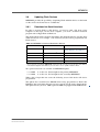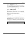
1
Embedded Solutions
20SC13-00 E3 - 2004-01-30
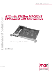
SC13 – 6U Busless PowerPC
SBC with Mezzanines
User Manual
Board-Level Computers
for Industrial Applications
®
SC13 – 6U Busless PowerPC SBC with Mezzanines
SC13 – 6U Busless PowerPC SBC with Mezzanines
The SC13 is a single-board computer for embedded applications based on the
Kahlua II PowerPC, offering different types of mezzanine slots for industrial and
computer I/O extensions.
The SC13 comes with the MPC8245 PowerPC with 300MHz clock frequency and a
local 32-bit/33-MHz PCI data bus. It is a complete state-of-the-art SBC offering
DRAM, Flash and CompactFlash memory, dual Fast Ethernet, 4 COMs, USB, IDE
and keyboard/mouse interfaces as well as an optional onboard hard disk.
In addition, the SC13 can be equipped with different types of standard mezzanine
cards. The modular combination of I/O functionality on a single-board computer
allows to build up tailored control systems which appear as customized solutions
based on standard components.
Depending on I/O requirements, you can use the most suitable of different standard
versions of SC13—with 3 M-Module or 3 PC•MIP or 2 PMC slots.
M-Modules are recommended for real-world I/O such as analog/binary process I/O
and instrumentation I/O. PC•MIP is the format of choice for all kinds of workstation
I/O like graphics, SCSI, Ethernet and further serial lines. PMC may be used
especially for intelligent telecom I/O.
Alternatively, the SC13 stand-alone SBC is available with a VME interface (A12) or
with a system-slot CompactPCI interface (D3).
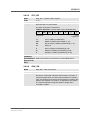
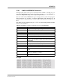
Technical Data
CPU
• Motorola PowerPC
- MPC8245
- 300MHz
Memory
•
•
•
•
Level 1 Cache integrated in MPC8245
SO-DIMM slot for up to 512MB SDRAM
100MHz memory bus operation
Flash 2MB
- 8-bit data bus
• Serial EEPROM 2KB for factory settings
• CompactFlash (TM) card interface for Flash ATA (true IDE) via on-board IDE
MEN Mikro Elektronik GmbH
20SC13-00 E3 - 2004-01-30
2
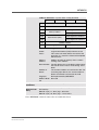
Technical Data
Interfaces
• Two 10/100Mbits/s Ethernet channels
- Intel 82559ER
- RJ45 at front panel with two LEDs
• One UART RS232 serial interface (COM1)
- 16-byte send/receive buffer
- RJ45 at front panel
• One UART (COM2)
- 16-byte send/receive buffer
- Physical interface using SA adapter via 10-pin ribbon cable on I/O connector
- RS232..RS485, isolated or not: for free use in system (e. g. cable to front)
• Two MPC8245 UARTs
- Accessible via I/O connector
• IDE port for hard disk drives
- Drive can be connected via ribbon cable or mounted directly on the CPU
board using MEN's adapter kit
- Only one CompactPCI slot needed even with hard disk
• Keyboard/mouse
- PS/2 compatible
- External adapters for line drivers required
• USB port
- External line drivers
Local PCI Bus
• PCI Spec. 2.2 compliant
• 32-bit data bus, 33MHz, 3.3V
Mezzanine Extensions
• SC13a: three PC-MIPs Type I/II on local PCI bus
- Compliant with PC-MIP specification
• SC13b: three M-Modules
- Compliant with M-Module standard
- Characteristics: D16, D32, A08, A24, INTA, INTC
• SC13c: two PMCs
- Compliant with PMC standard IEEE P1386
Miscellaneous
•
•
•
•
•
•
Serial real-time clock with integrated 56-byte NVRAM
Serial hardware watchdog in supervisory circuit
Power supply via onboard 4-pin power connector
Temperature sensor
Hex switch for user settings
User LEDs (external)
MEN Mikro Elektronik GmbH
20SC13-00 E3 - 2004-01-30
3
Technical Data
Electrical Specifications
• Supply voltage/power consumption:
- +5V (4.85V..5.25V), 1.65 A typ.
- ±12V for mezzanines only, tbd.
• MTBF: 63,000h @ 50°C
Mechanical Specifications
• Dimensions: standard double Eurocard, 233.3mm x 160mm
• Weight (without mezzanines and accessories):
- SC13a: 242g
- SC13b: 240g
- SC13c: 237g
Environmental Specifications
• Temperature range (operation):
- 0..+60°C or -40..+85°C
- Airflow: min. 10m³/h
• Temperature range (storage): -40..+85°C
• Relative humidity (operation): max. 95% non-condensing
• Relative humidity (storage): max. 95% non-condensing
• Altitude: -300m to + 3,000m
• Shock: 15g/11ms
• Bump: 10g/16ms
• Vibration (sinusoidal): 2g/10..150Hz
Safety
• PCB manufactured with a flammability rating of 94V-0 by UL recognized manufacturers
EMC
• Tested according to EN 55022 (radio disturbance), IEC1000-4-2 (ESD) and
IEC1000-4-4 (burst) with regard to CE conformity
Software Support
•
•
•
•
VxWorks
OS-9
Linux
MENMON
MEN Mikro Elektronik GmbH
20SC13-00 E3 - 2004-01-30
4
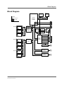
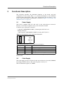
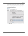
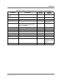
Block Diagram
Block Diagram
2MB Boot/
Application
Flash
SO-DIMM
DRAM
Legend
F
Front Panel
B
On Board
SC13b
PowerPC
MPC8245
@ 300MHz
M-Module
64-bit Data Bus
COM3
B
COM4
B
FPGA User
Function
B
F
M-Module
PCI-toM-Module
Bridge
Temp.
Sensor
Watchdog/
EEPROM
CompactFlash
B
F
RTC
I²C
M-Module
F
IDE
IDE
SC13a
PCI-to-ISA Mouse/Keyboard
Bridge
USB
Super I/O
PC•MIP
PCI-to-PCI
Bridge
F
COM2
B
B
B
B
COM1
PC•MIP
F
RS232
F
10/100Base-T
Ethernet
F
10/100Base-T
Ethernet
F
PC•MIP
F
SC13c
PMC
F
PMC
F
MEN Mikro Elektronik GmbH
20SC13-00 E3 - 2004-01-30
5
Product Safety
Product Safety
!
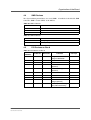
Fuses
This board contains fuses. If you need to replace a fuse, make sure you adhere to the
following types and ratings:
Component
Current Rating
Type
Size
S1
3A
Fast
1206
S2
1.5A
Fast
1206
For component locations, see Chapter 5.3 Component Plans on page 84.
!
Electrostatic Discharge (ESD)
Computer boards and components contain electrostatic sensitive devices.
Electrostatic discharge (ESD) can damage components. To protect the board and
other components against damage from static electricity, you should follow some
precautions whenever you work on your computer.
• Power down and unplug your computer system when working on the inside.
• Hold components by the edges and try not to touch the IC chips, leads, or circuitry.
• Use a grounded wrist strap before handling computer components.
• Place components on a grounded antistatic pad or on the bag that came with the
component whenever the components are separated from the system.
• Store the board only in its original ESD-protected packaging. Retain the original
packaging in case you need to return the board to MEN for repair.
MEN Mikro Elektronik GmbH
20SC13-00 E3 - 2004-01-30
6
About this Document
About this Document
This user manual describes the hardware functions of the board, connection of
peripheral devices and integration into a system. It also provides additional
information for special applications and configurations of the board.
The manual does not include detailed information on individual components (data
sheets etc.). A list of literature is given in the appendix.
The SC13 board is an SBC with a large scope of options regarding installation
and combination of mezzanines. There are three main models of the board:
SC13a with PC•MIP modules, SC13b with M-Modules, and SC13c with PMCs.
This manual describes all of these three models and generally refers to the
board as "SC13".
History
Edition
Description
Technical Content
Date of Issue
E1
First edition
H. Schubert, K. Popp
2001-12-17
E2
Second edition
H. Schubert, K. Popp
2002-12-06
E3
Third edition
H. Schubert, K. Popp
2004-01-30
Conventions
!
italics
bold
hyperlink
This sign marks important notes or warnings concerning proper functionality of the
product described in this document. You should read them in any case.
Folder and file names are printed in italics.
Bold type is used for emphasis.
Hyperlinks are printed in blue color.
The globe will show you where hyperlinks lead directly to the Internet, so you can
look for the latest information online.
0xFF
Hexadecimal numbers are preceded by "0x", which is the usual C-language
convention, and are printed in a monospace type, e.g. 0x00FFFF.
IRQ#
/IRQ
Signal names followed by "#" or preceded by a slash ("/") indicate that this signal is
either active low or that it becomes active at a falling edge.
in/out
Signal directions in signal mnemonics tables generally refer to the corresponding
board or component, "in" meaning "to the board or component", "out" meaning
"coming from it".
Vertical lines on the outer margin signal technical changes to the previous edition of
the document.
MEN Mikro Elektronik GmbH
20SC13-00 E3 - 2004-01-30
7
About this Document
Copyright Information
MEN reserves the right to make changes without further notice to any products herein. MEN makes no
warranty, representation or guarantee regarding the suitability of its products for any particular
purpose, nor does MEN assume any liability arising out of the application or use of any product or
circuit, and specifically disclaims any and all liability, including without limitation consequential or
incidental damages.
"Typical" parameters can and do vary in different applications. All operating parameters, including
"Typicals" must be validated for each customer application by customer's technical experts.
MEN does not convey any license under its patent rights nor the rights of others.
MEN products are not designed, intended, or authorized for use as components in systems intended for
surgical implant into the body, or other applications intended to support or sustain life, or for any other
application in which the failure of the MEN product could create a situation where personal injury or
death may occur. Should Buyer purchase or use MEN products for any such unintended or
unauthorized application, Buyer shall indemnify and hold MEN and its officers, employees,
subsidiaries, affiliates, and distributors harmless against all claims, costs, damages, and expenses, and
reasonable attorney fees arising out of, directly or indirectly, any claim of personal injury or death
associated with such unintended or unauthorized use, even if such claim alleges that MEN was
negligent regarding the design or manufacture of the part.
All brand or product names are trademarks or registered trademarks of their respective holders.
Information in this document has been carefully checked and is believed to be accurate as of the date of
publication; however, no responsibility is assumed for inaccuracies. MEN will not be liable for any
consequential or incidental damages arising from reliance on the accuracy of this document. The
information contained herein is subject to change without notice.
Copyright © 2004 MEN Mikro Elektronik GmbH. All rights reserved.
Please recycle
Germany
MEN Mikro Elektronik GmbH
Neuwieder Straße 5-7
90411 Nuremberg
Phone +49-911-99 33 5-0
Fax +49-911-99 33 5-901
E-mail [email protected]
www.men.de
France
MEN Mikro Elektronik SA
18, rue René Cassin
ZA de la Châtelaine
74240 Gaillard
Phone +33 (0) 450-955-312
Fax +33 (0) 450-955-211
E-mail [email protected]
www.men-france.fr
MEN Mikro Elektronik GmbH
20SC13-00 E3 - 2004-01-30
UK
MEN Micro Ltd
Whitehall, 75 School Lane
Hartford, Northwich
Cheshire UK, CW8 1PF
Phone +44 (0) 1477-549-185
Fax +44 (0) 1477-549-178
E-mail [email protected]
www.menmicro.co.uk
USA
MEN Micro, Inc.
3740 North Josey Lane, Suite 203
Carrollton, TX 75007
Phone 972-939-2675
Fax 972-939-0055
E-mail [email protected]
www.menmicro.com
8
Contents
Contents
1 Getting Started . . . . . . . . . . . . . . . . . . . . . . . . . . . . . . . . . . . . . . . . . . . . . . . .
1.1 Maps of the Board . . . . . . . . . . . . . . . . . . . . . . . . . . . . . . . . . . . . . . . .
1.2 Configuring the Hardware . . . . . . . . . . . . . . . . . . . . . . . . . . . . . . . . . .
1.3 Integrating the Board into a System . . . . . . . . . . . . . . . . . . . . . . . . . .
1.4 Installing Operating System Software. . . . . . . . . . . . . . . . . . . . . . . . .
14
14
18
19
19
2 Functional Description . . . . . . . . . . . . . . . . . . . . . . . . . . . . . . . . . . . . . . . . . .
2.1 Power Supply. . . . . . . . . . . . . . . . . . . . . . . . . . . . . . . . . . . . . . . . . . . .
2.2 Clock Supply . . . . . . . . . . . . . . . . . . . . . . . . . . . . . . . . . . . . . . . . . . . .
2.3 PowerPC CPU . . . . . . . . . . . . . . . . . . . . . . . . . . . . . . . . . . . . . . . . . . .
2.3.1
General . . . . . . . . . . . . . . . . . . . . . . . . . . . . . . . . . . . . . . . . .
2.3.2
Heat Sink. . . . . . . . . . . . . . . . . . . . . . . . . . . . . . . . . . . . . . . .
2.4 Bus Structure . . . . . . . . . . . . . . . . . . . . . . . . . . . . . . . . . . . . . . . . . . . .
2.4.1
Host-to-PCI Bridge . . . . . . . . . . . . . . . . . . . . . . . . . . . . . . . .
2.4.2
Local PCI Bus . . . . . . . . . . . . . . . . . . . . . . . . . . . . . . . . . . . .
2.4.3
PCI-to-ISA Bridge Super I/O Controller . . . . . . . . . . . . . . .
2.4.4
PCI-to-PCI Bridge. . . . . . . . . . . . . . . . . . . . . . . . . . . . . . . . .
2.5 Memory . . . . . . . . . . . . . . . . . . . . . . . . . . . . . . . . . . . . . . . . . . . . . . . .
2.5.1
SDRAM . . . . . . . . . . . . . . . . . . . . . . . . . . . . . . . . . . . . . . . .
2.5.2
Flash . . . . . . . . . . . . . . . . . . . . . . . . . . . . . . . . . . . . . . . . . . .
2.5.3
CompactFlash . . . . . . . . . . . . . . . . . . . . . . . . . . . . . . . . . . . .
2.5.4
EEPROM. . . . . . . . . . . . . . . . . . . . . . . . . . . . . . . . . . . . . . . .
2.6 PC•MIP Slots (SC13a) . . . . . . . . . . . . . . . . . . . . . . . . . . . . . . . . . . . .
2.6.1
Installing a PC•MIP Mezzanine Module . . . . . . . . . . . . . . .
2.6.2
PC•MIP Connectors . . . . . . . . . . . . . . . . . . . . . . . . . . . . . . .
2.7 M-Module Slots (SC13b) . . . . . . . . . . . . . . . . . . . . . . . . . . . . . . . . . .
2.7.1
Connection . . . . . . . . . . . . . . . . . . . . . . . . . . . . . . . . . . . . . .
2.7.2
Addressing the M-Modules. . . . . . . . . . . . . . . . . . . . . . . . . .
2.7.3
Installing an M-Module Mezzanine Module . . . . . . . . . . . .
2.8 PMC Slots (SC13c) . . . . . . . . . . . . . . . . . . . . . . . . . . . . . . . . . . . . . . .
2.8.1
Installing a PMC Mezzanine Module . . . . . . . . . . . . . . . . . .
2.9 IDE Interface . . . . . . . . . . . . . . . . . . . . . . . . . . . . . . . . . . . . . . . . . . . .
2.9.1
Installing a Hard Disk . . . . . . . . . . . . . . . . . . . . . . . . . . . . . .
2.10 Ethernet Interface . . . . . . . . . . . . . . . . . . . . . . . . . . . . . . . . . . . . . . . .
2.10.1 Connection . . . . . . . . . . . . . . . . . . . . . . . . . . . . . . . . . . . . . .
2.10.2 General . . . . . . . . . . . . . . . . . . . . . . . . . . . . . . . . . . . . . . . . .
2.10.3 10Base-T . . . . . . . . . . . . . . . . . . . . . . . . . . . . . . . . . . . . . . . .
2.10.4 100Base-T . . . . . . . . . . . . . . . . . . . . . . . . . . . . . . . . . . . . . . .
2.11 I/O Connector . . . . . . . . . . . . . . . . . . . . . . . . . . . . . . . . . . . . . . . . . . .
2.11.1 Making the Interfaces Available . . . . . . . . . . . . . . . . . . . . . .
2.12 Serial Ports COM1..COM4 . . . . . . . . . . . . . . . . . . . . . . . . . . . . . . . . .
2.12.1 COM1 . . . . . . . . . . . . . . . . . . . . . . . . . . . . . . . . . . . . . . . . . .
2.12.2 COM2..COM4 . . . . . . . . . . . . . . . . . . . . . . . . . . . . . . . . . . .
20
20
20
21
21
21
22
22
22
22
22
23
23
24
24
25
26
26
27
28
28
29
30
31
31
32
34
36
36
37
37
37
38
40
41
41
41
MEN Mikro Elektronik GmbH
20SC13-00 E3 - 2004-01-30
9
Contents
2.13
2.14
2.15
2.16
Temperature Sensor . . . . . . . . . . . . . . . . . . . . . . . . . . . . . . . . . . . . . . .
Real-Time Clock and NVRAM . . . . . . . . . . . . . . . . . . . . . . . . . . . . . .
Watchdog . . . . . . . . . . . . . . . . . . . . . . . . . . . . . . . . . . . . . . . . . . . . . . .
User-Defined Hex Switch . . . . . . . . . . . . . . . . . . . . . . . . . . . . . . . . . .
43
43
43
43
3 MENMON . . . . . . . . . . . . . . . . . . . . . . . . . . . . . . . . . . . . . . . . . . . . . . . . . . . .
3.1 General . . . . . . . . . . . . . . . . . . . . . . . . . . . . . . . . . . . . . . . . . . . . . . . .
3.2 Console . . . . . . . . . . . . . . . . . . . . . . . . . . . . . . . . . . . . . . . . . . . . . . . .
3.3 MENMON Memory Map . . . . . . . . . . . . . . . . . . . . . . . . . . . . . . . . . .
3.4 MENMON Start-up . . . . . . . . . . . . . . . . . . . . . . . . . . . . . . . . . . . . . . .
3.4.1
User LEDs. . . . . . . . . . . . . . . . . . . . . . . . . . . . . . . . . . . . . . .
3.4.2
Boot Sequence. . . . . . . . . . . . . . . . . . . . . . . . . . . . . . . . . . . .
3.4.3
Configuring the MENMON Start-up Procedure . . . . . . . . . .
3.4.4
Self Tests . . . . . . . . . . . . . . . . . . . . . . . . . . . . . . . . . . . . . . . .
3.5 MENMON Boot Methods for Client Programs . . . . . . . . . . . . . . . . .
3.5.1
MENMON BIOS Devices. . . . . . . . . . . . . . . . . . . . . . . . . . .
3.5.2
Disk Boot . . . . . . . . . . . . . . . . . . . . . . . . . . . . . . . . . . . . . . .
3.5.3
Network Boot . . . . . . . . . . . . . . . . . . . . . . . . . . . . . . . . . . . .
3.6 Updating Flash Devices. . . . . . . . . . . . . . . . . . . . . . . . . . . . . . . . . . . .
3.6.1
Download via Serial Interface. . . . . . . . . . . . . . . . . . . . . . . .
3.6.2
Performing the Download . . . . . . . . . . . . . . . . . . . . . . . . . . .
3.6.3
Update from Disk or Network. . . . . . . . . . . . . . . . . . . . . . . .
3.7 MENMON User Interface . . . . . . . . . . . . . . . . . . . . . . . . . . . . . . . . . .
3.7.1
Command Line Editing . . . . . . . . . . . . . . . . . . . . . . . . . . . . .
3.7.2
Numerical Arguments . . . . . . . . . . . . . . . . . . . . . . . . . . . . . .
3.7.3
MENMON Command Overview . . . . . . . . . . . . . . . . . . . . .
3.8 Board Setup . . . . . . . . . . . . . . . . . . . . . . . . . . . . . . . . . . . . . . . . . . . . .
3.8.1
ALI 1543 . . . . . . . . . . . . . . . . . . . . . . . . . . . . . . . . . . . . . . . .
3.8.2
PCI Auto-Configuration . . . . . . . . . . . . . . . . . . . . . . . . . . . .
3.8.3
SDRAM DIMM Configuration. . . . . . . . . . . . . . . . . . . . . . .
3.8.4
Watchdog Configuration . . . . . . . . . . . . . . . . . . . . . . . . . . . .
3.8.5
Hex Switch . . . . . . . . . . . . . . . . . . . . . . . . . . . . . . . . . . . . . .
3.9 MENMON System Calls . . . . . . . . . . . . . . . . . . . . . . . . . . . . . . . . . . .
3.9.1
Invoking System Calls. . . . . . . . . . . . . . . . . . . . . . . . . . . . . .
3.9.2
System Calls . . . . . . . . . . . . . . . . . . . . . . . . . . . . . . . . . . . . .
3.10 VxWorks Bootline . . . . . . . . . . . . . . . . . . . . . . . . . . . . . . . . . . . . . . . .
3.10.1 Additional MENMON Parameters . . . . . . . . . . . . . . . . . . . .
44
44
44
45
46
46
46
46
47
49
49
51
56
58
58
59
60
61
61
61
62
64
64
64
66
66
66
67
67
68
72
74
4 Organization of the Board . . . . . . . . . . . . . . . . . . . . . . . . . . . . . . . . . . . . . . .
4.1 Memory Mappings . . . . . . . . . . . . . . . . . . . . . . . . . . . . . . . . . . . . . . .
4.1.1
Processor View of the Memory Map. . . . . . . . . . . . . . . . . . .
4.1.2
PCI/ISA I/O Space Memory Map . . . . . . . . . . . . . . . . . . . . .
4.2 Interrupt Handling . . . . . . . . . . . . . . . . . . . . . . . . . . . . . . . . . . . . . . . .
4.2.1
Nonmaskable Interrupts . . . . . . . . . . . . . . . . . . . . . . . . . . . .
4.2.2
Maskable Interrupts. . . . . . . . . . . . . . . . . . . . . . . . . . . . . . . .
75
75
75
77
78
78
78
MEN Mikro Elektronik GmbH
20SC13-00 E3 - 2004-01-30
10
Contents
4.3
4.4
4.5
4.6
4.7
Implementation of M1543 PCI-to-ISA Bridge . . . . . . . . . . . . . . . . . .
SMB Devices . . . . . . . . . . . . . . . . . . . . . . . . . . . . . . . . . . . . . . . . . . . .
PCI Devices on Bus 0 . . . . . . . . . . . . . . . . . . . . . . . . . . . . . . . . . . . . .
PCI Devices on PC•MIP/PMC Bus . . . . . . . . . . . . . . . . . . . . . . . . . . .
M-Module Interface. . . . . . . . . . . . . . . . . . . . . . . . . . . . . . . . . . . . . . .
79
80
80
81
81
5 Appendix . . . . . . . . . . . . . . . . . . . . . . . . . . . . . . . . . . . . . . . . . . . . . . . . . . . . .
5.1 Literature and WWW Resources. . . . . . . . . . . . . . . . . . . . . . . . . . . . .
5.1.1
PowerPC . . . . . . . . . . . . . . . . . . . . . . . . . . . . . . . . . . . . . . . .
5.1.2
Bridges . . . . . . . . . . . . . . . . . . . . . . . . . . . . . . . . . . . . . . . . .
5.1.3
PC•MIP . . . . . . . . . . . . . . . . . . . . . . . . . . . . . . . . . . . . . . . . .
5.1.4
M-Modules . . . . . . . . . . . . . . . . . . . . . . . . . . . . . . . . . . . . . .
5.1.5
PMC . . . . . . . . . . . . . . . . . . . . . . . . . . . . . . . . . . . . . . . . . . .
5.1.6
Ethernet . . . . . . . . . . . . . . . . . . . . . . . . . . . . . . . . . . . . . . . . .
5.1.7
EIDE . . . . . . . . . . . . . . . . . . . . . . . . . . . . . . . . . . . . . . . . . . .
5.1.8
USB . . . . . . . . . . . . . . . . . . . . . . . . . . . . . . . . . . . . . . . . . . . .
5.2 Board Revisions. . . . . . . . . . . . . . . . . . . . . . . . . . . . . . . . . . . . . . . . . .
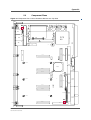
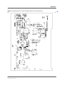
5.3 Component Plans. . . . . . . . . . . . . . . . . . . . . . . . . . . . . . . . . . . . . . . . .
82
82
82
82
82
82
82
82
83
83
83
84
MEN Mikro Elektronik GmbH
20SC13-00 E3 - 2004-01-30
11
Figures
Figure 1. General Board Map—Top View . . . . . . . . . . . . . . . . . . . . . . . . . . . . .
Figure 2. SC13a Board Map—CPU Board with PC•MIPs - Top View . . . . . . .
Figure 3. SC13b Board Map—CPU Board with M-Modules - Top View . . . . .
Figure 4. SC13c Board Map—CPU Board with PMCs - Top View . . . . . . . . . .
Figure 5. SO-DIMM DRAM Installation . . . . . . . . . . . . . . . . . . . . . . . . . . . . . .
Figure 6. Installing a CompactFlash Card . . . . . . . . . . . . . . . . . . . . . . . . . . . . . .
Figure 7. Installing a PC•MIP Mezzanine Module . . . . . . . . . . . . . . . . . . . . . . .
Figure 8. Installing an M-Module Mezzanine Module . . . . . . . . . . . . . . . . . . . .
Figure 9. Installing a PMC Mezzanine Module . . . . . . . . . . . . . . . . . . . . . . . . . .
Figure 10. A12C (VMEbus-family board) with Hard-Disk Adapter and
Hard Disk . . . . . . . . . . . . . . . . . . . . . . . . . . . . . . . . . . . . . . . . . . . . . . .
Figure 11. Position of Hard-Disk Adapter Card on the Board. . . . . . . . . . . . . . . .
Figure 12. Position of Hex Switch . . . . . . . . . . . . . . . . . . . . . . . . . . . . . . . . . . . . .
Figure 13. MENMON Address Mapping . . . . . . . . . . . . . . . . . . . . . . . . . . . . . . .
Figure 14. MENMON—Layout of the 0x41-Type Partition (PReP) . . . . . . . . . .
Figure 15. MENMON—Example PCI Configuration . . . . . . . . . . . . . . . . . . . . . .
Figure 16. Component Plan of SC13 Hardware Revision 03—Top Side . . . . . . .
Figure 17. Component Plan of SC13 Hardware Revision 03—Bottom Side . . . .
MEN Mikro Elektronik GmbH
20SC13-00 E3 - 2004-01-30
14
15
16
17
23
24
26
30
31
34
35
43
45
51
65
84
85
12
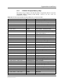
Tables
Table 1.
Table 2.
Table 3.
Table 4.
Table 5.
Table 6.
Table 7.
Table 8.
Table 9.
Table 10.
Table 11.
Table 12.
Table 13.
Table 14.
Table 15.
Table 16.
Table 17.
Table 18.
Table 19.
Table 20.
Table 21.
Table 22.
Table 23.
Table 24.
Table 25.
Table 26.
Table 27.
Table 28.
Table 29.
Table 30.
Table 31.
Table 32.
Table 33.
Table 34.
Table 35.
MEN Mikro Elektronik GmbH
20SC13-00 E3 - 2004-01-30
Pin Assignment of the 4-pin Power Connector . . . . . . . . . . . . . . . . . . 20
Signal Mnemonics for the 4-pin Power Connector . . . . . . . . . . . . . . . 20
Pin Assignment of the 60-Pin M-Module Plug Connectors . . . . . . . . . 28
M-Module Address Map . . . . . . . . . . . . . . . . . . . . . . . . . . . . . . . . . . . 29
Pin Assignment of the 44-Pin IDE Connector . . . . . . . . . . . . . . . . . . . 32
Signal Mnemonics for the IDE Connector . . . . . . . . . . . . . . . . . . . . . . 33
Pin Assignment and Status LEDs of the 8-pin RJ45 Ethernet 10Base-T/
100Base-T Connectors . . . . . . . . . . . . . . . . . . . . . . . . . . . . . . . . . . . . . 36
Signal Mnemonics of the Ethernet 10Base-T/100Base-T Connectors . 36
Pin Assignment of the 40-pin I/O Connector . . . . . . . . . . . . . . . . . . . . 39
Signal Mnemonics of 40-pin I/O Connector . . . . . . . . . . . . . . . . . . . . 39
Pin Assignment of 8-pin RJ45 RS232 Connector (COM1) . . . . . . . . . 41
MENMON - Assignment for Board Controller Devices . . . . . . . . . . . 50
MENMON—Download Destination Devices . . . . . . . . . . . . . . . . . . . 58
MENMON—Flash Sectors. . . . . . . . . . . . . . . . . . . . . . . . . . . . . . . . . . 59
MENMON Command Overview . . . . . . . . . . . . . . . . . . . . . . . . . . . . . 62
Hex-Switch Settings . . . . . . . . . . . . . . . . . . . . . . . . . . . . . . . . . . . . . . . 66
MENMON—System Calls—BRD_ID Fields . . . . . . . . . . . . . . . . . . . 68
MENMON—System Calls—RTC_RD Buffer Data . . . . . . . . . . . . . . 70
MENMON—System Calls—DSK_RD Fields. . . . . . . . . . . . . . . . . . . 71
MENMON—VxWorks Bootline—List of Parameters and their Usage 73
MENMON—Common Parameters Passed by All MENMONs. . . . . . 74
Memory Map—Processor View . . . . . . . . . . . . . . . . . . . . . . . . . . . . . . 75
Address Mapping for PCI. . . . . . . . . . . . . . . . . . . . . . . . . . . . . . . . . . . 75
BATS set up by MENMON . . . . . . . . . . . . . . . . . . . . . . . . . . . . . . . . . 76
PCI/ISA I/O Space Memory Map (addresses as seen from CPU) . . . . 77
Interrupts on the CPU Board . . . . . . . . . . . . . . . . . . . . . . . . . . . . . . . . 78
M1543 General Purpose Input (GPI) Pin Assignments . . . . . . . . . . . . 79
M1543 General Purpose Output (GPO) Pin Assignments . . . . . . . . . . 79
M1543 General Purpose Input/Output (GPIO) Pin Assignments . . . . 79
SMB 1 Devices. . . . . . . . . . . . . . . . . . . . . . . . . . . . . . . . . . . . . . . . . . . 80
SMB 2 Devices. . . . . . . . . . . . . . . . . . . . . . . . . . . . . . . . . . . . . . . . . . . 80
PCI Devices on Bus 0. . . . . . . . . . . . . . . . . . . . . . . . . . . . . . . . . . . . . . 80
PCI Devices on PC•MIP/PMC Bus . . . . . . . . . . . . . . . . . . . . . . . . . . . 81
M-Module Device Addresses . . . . . . . . . . . . . . . . . . . . . . . . . . . . . . . . 81
Table of Hardware Revisions . . . . . . . . . . . . . . . . . . . . . . . . . . . . . . . . 83
13
Getting Started
1
Getting Started
This chapter will give an overview of the board and some hints for first installation
in a system as a "check list".
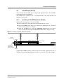
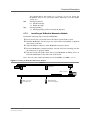
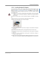
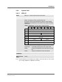
1.1
Maps of the Board
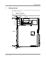
Figure 1. General Board Map—Top View
VMEbus P1 (A12 board family)
Ethernet
10Base-T 1
CompactFlash
card connector
SO-DIMM
DRAM Socket
MPC8245
1
Ethernet
10Base-T 2
Production/Test
Userconfigurable
hex switch
Power Connector
(SC13 family)
Reset Button/LED
RS232
COM1
I/O Connector
Front-panel
mounting screw
Front Panel
Side of Board
CompactPCI J1/J2 (D3 board family)
M1543
ALI
IDE Interface
Front-panel
mounting screw
MEN Mikro Elektronik GmbH
20SC13-00 E3 - 2004-01-30
14
Getting Started
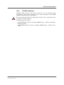
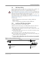
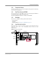
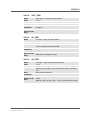
Figure 2. SC13a Board Map—CPU Board with PC•MIPs - Top View
SO-DIMM
DRAM Socket
MPC8245
Ethernet
10Base-T 2
Production/Test
Userconfigurable
hex switch
Power Connector
(SC13 family)
Ethernet
10Base-T 1
1
I/O Connector
Reset Button/LED
RS232
COM1
CompactFlash
card connector
VMEbus P1 (A12 board family)
Front-panel
mounting screw
PC•MIP
Slot 2
Front Panel
Side of Board
M1543
ALI
CompactPCI J1/J2 (D3 board family)
PC•MIP Bezel
Keepers
PC•MIP
Slot 1
PC•MIP
Keeper Screw
(solder side)
Finished Bezel
of PC•MIP I/O
Connector
PC•MIP
Slot 0
IDE Interface
Front-panel
mounting screw Injectors/Ejectors with
Threaded Standoffs and
Captive Screws
MEN Mikro Elektronik GmbH
20SC13-00 E3 - 2004-01-30
15
Getting Started
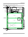
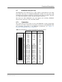
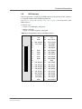
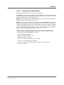
Figure 3. SC13b Board Map—CPU Board with M-Modules - Top View
I/O Connector
SO-DIMM
DRAM Socket
MPC8245
1
Ethernet
10Base-T 2
Production/Test
Userconfigurable
hex switch
M-Module 2
Power Connector
(SC13 family)
Ethernet
10Base-T 1
60-pin plug connector
Reset Button/LED
RS232
COM1
CompactFlash
card connector
VMEbus P1 (A12 board family)
Front-panel
mounting screw
Holes for M-Module
Mounting Screws
60-pin plug connector
M-Module 1
M-Module 0
CompactPCI J1/J2 (D3 board family)
M1543
ALI
60-pin plug connector
Front Panel
Side of Board
IDE Interface
Front-panel
mounting screw
MEN Mikro Elektronik GmbH
20SC13-00 E3 - 2004-01-30
16
Getting Started
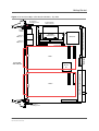
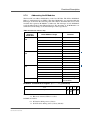
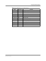
Figure 4. SC13c Board Map—CPU Board with PMCs - Top View
I/O Connector
Ethernet
10Base-T 1
SO-DIMM
DRAM Socket
MPC8245
1
Ethernet
10Base-T 2
Userconfigurable
hex switch
Production/Test
Power Connector
(SC13 family)
Reset Button/LED
RS232
COM1
CompactFlash
card connector
VMEbus P1 (A12 board family)
Front-panel
mounting screw
PMC 1
Front Panel
Side of Board
CompactPCI J1/J2 (D3 board family)
M1543
ALI
PMC 0
IDE Interface
Front-panel
mounting screw
MEN Mikro Elektronik GmbH
20SC13-00 E3 - 2004-01-30
17
Getting Started
1.2
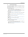
Configuring the Hardware
You should check your hardware requirements before installing the board in a
system, since most modifications are difficult or even impossible to do when the
board is mounted in an enclosure.
The following check list will give an overview on what you might want to configure.
DRAM SO-DIMM modules
The board is shipped without any DRAM on board. You should check your
main memory needs and install a suitable SO-DIMM module.
Refer to Chapter 2.5.1 SDRAM on page 23 for a detailed installation
description and hints on supported SO-DIMM modules.
CompactFlash
Refer to Chapter 2.5.3 CompactFlash on page 24 for a detailed
installation description and hints on supported CompactFlash cards.
PC•MIPs
Refer to Chapter 2.6.1 Installing a PC•MIP Mezzanine Module on page
26 for a detailed installation description.
M-Modules
Refer to Chapter 2.7.3 Installing an M-Module Mezzanine Module on
page 30 for a detailed installation description.
PMC modules
Refer to Chapter 2.8.1 Installing a PMC Mezzanine Module on page 31
for a detailed installation description.
Serial interface (SA) adapters
You can install standard serial interfaces such as RS232 using MEN’s SA
adapters on the SC13’s COM2..COM4 UART connectors.
Refer to Chapter 2.12 Serial Ports COM1..COM4 on page 41 for detailed
installation descriptions.
MEN Mikro Elektronik GmbH
20SC13-00 E3 - 2004-01-30
18
Getting Started
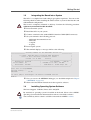
1.3
Integrating the Board into a System
The SC13 is a complex board and setting it up requires experience. You can use the
following check list when installing the CPU board in a system for the first time and
with minimum configuration.
!
The board is completely trimmed on delivery. Perform the following procedure
without any mezzanine module installed!
Power-down the system.
Install the SC13 in your system.
Connect a terminal to the standard RS232 interface COM1 (RJ45 connector).
Set your terminal to the following protocol:
-
9600 baud data transmission rate
8 data bits
1 stop bit
no parity
Power-up the system.
The terminal displays a message similar to the following:
_________________ Secondary MenMon for the A012/D003 Version 2.0 ____________
|
|
|
(c) 1999 - 2001 MEN mikro elektronik GmbH Nuernberg
|
|
Parts of this code based on Motorola's Dink32
|
|
Created Jul 11 2001
15:24:33
|
|_____________________________________________________________________________|
|
HW Revision: 01.00.00
|
CPU: MPC8245
(MAP B)
|
| Serial Number: 44
| CPU/MEM Clock: 300 / 100 MHz
|
|
Board Model: SC13b00
|
DIMM Module: 64 MB Setup: 222
|
\___________________________________________________________________________/
press 'ESC' to setup/MENMON
Selftest running ...
CHECKSUM
==> OK
*** Can't jump to bootstrapper. BS address in EEPROM invalid!
MenMon>
Now you can use the MENMON debugger (see detailed description in Chapter
3 MENMON on page 44).
Observe the installation instructions for the respective software.
1.4
Installing Operating System Software
The board supports VxWorks, Linux, OS-9 and QNX.
!
By standard, no operating system is installed on the board. Please refer to MEN’s
operating system installation documentation on how to install the software!
You can find any driver software available for download on MEN’s website.
MEN Mikro Elektronik GmbH
20SC13-00 E3 - 2004-01-30
19
Functional Description
2
Functional Description
The following describes the individual functions of the board and their
configuration on the board. There is no detailed description of the individual
controller chips and the CPUs. They can be obtained from the data sheets or data
books of the semiconductor manufacturer concerned (Chapter 5.1 Literature and
WWW Resources on page 82).
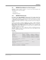
2.1
Power Supply
The board is supplied with +5V and ±12V via the onboard power connector.
However, ±12V may be required only by some mezzanine modules.
Connector types 4-pin power connector:
• 4-pin plug, AMP MATE-N-LOK™, 5.08mm pitch, P/N 350 211-1
• Mating connector:
4-pin receptacle, AMP MATE-N-LOK™, housing, P/N 770 827-1
Table 1. Pin Assignment of the 4-pin Power Connector
4
+5V
3
3
GND
2
2
GND12V
1
+12V
4
1
Table 2. Signal Mnemonics for the 4-pin Power Connector
Signal
Direction
Function
+12V
-
+12V power supply
+5V
-
+5V power supply
GND
-
Digital ground
GND12V
-
Digital ground of +12V supply
The onboard power supply generates the 2.0V core voltage and 3.3V I/O voltage of
the PowerPC.
2.2
Clock Supply
The clock supply generates all clocks for the on-board devices (PowerPC, SDRAM,
host bridge, PCI bus devices). The clock frequency is factory-set.
The local PCI clock operates at 33MHz.
MEN Mikro Elektronik GmbH
20SC13-00 E3 - 2004-01-30
20
Functional Description
2.3
PowerPC CPU
The board is equipped with the MPC8245 Kahlua II processor, which includes a 32bit superscalar PowerPC 603e core, the integrated host-to-PCI bridge, and two
UARTs.
2.3.1
General
The PowerPC architecture, developed jointly by Motorola, IBM, and Apple
Computer, is based on the POWER architecture implemented by the RS/6000™
family of computers. The PowerPC architecture takes advantage of recent
technological advances in such areas as process technology, compiler design, and
RISC microprocessor design to provide software compatibility across a diverse
family of implementations, primarily single-chip microprocessors, intended for a
wide range of systems.
2.3.2
Heat Sink
A heat sink is provided to meet thermal requirements.
MEN Mikro Elektronik GmbH
20SC13-00 E3 - 2004-01-30
21
Functional Description
2.4
Bus Structure
2.4.1
Host-to-PCI Bridge
The integrated host-to-PCI bridge (internal in MPC8245) is used as host bridge and
memory controller for the PowerPC processor. All transactions of the PowerPC to
the PCI bus are controlled by the host bridge. The SDRAM and boot Flash are
connected to the local memory bus of the integrated host-to-PCI bridge.
The PCI interface is PCI bus Rev. 2.2 compliant and supports all bus commands and
transactions. Master and target operations are possible. Only big-endian operation is
supported.
2.4.2
Local PCI Bus
The local PCI bus is controlled by the integrated host-to-PCI bridge. It runs at
33MHz. The I/O voltage is fixed to 3.3V. The data width is 32 bits.
Major functional elements of the board, such as Ethernet, are connected to the local
PCI bus.
2.4.3
PCI-to-ISA Bridge Super I/O Controller
The M1543 provides integrated Super I/O (2 serial ports), system peripherals (ISP)
(2 82C59 and serial interrupt, 1 82C54), advanced features (type F and distributed
DMA) in the DMA controller (2 82C37), PS2 keyboard/mouse controller, 2-channel
dedicated IDE master controller with Ultra-33 specification and System
Management Bus (SMB).
M1543 also provides a PCI-to-ISA IRQ routing table, and level-to-edge trigger
transfer.
2.4.4
PCI-to-PCI Bridge
The SC13a and SC13c boards have a secondary PCI bus for accesses to PC•MIP
and PMC modules. It is controlled by a PCI-to-PCI bridge of type 2031 from TI.
MEN Mikro Elektronik GmbH
20SC13-00 E3 - 2004-01-30
22
Functional Description
2.5
Memory
2.5.1
SDRAM
One SDRAM bank (bank 0) is implemented on the board. Bank 0 is connected to a
144-pin SO-DIMM connector. The current board version supports SO-DIMMs up to
512MB.
2.5.1.1
Installing SO-DIMM DRAM
The board is shipped without any DRAM SO-DIMM module installed. To install a
SO-DIMM module, please stick to the following procedure.
Figure 5. SO-DIMM DRAM Installation
SO-DIMM Memory Module
Safety Notch
Clip
Contact
Groove
Clip
Safety Tab
SO-DIMM Socket
The DRAM module will only fit as shown above because of a safety tab on the SODIMM socket which requires a notch in the SO-DIMM module.
!
Power down the system before installing a SO-DIMM module to avoid damage
of the board!
Place the memory module into the socket at a 45° angle and make sure that the
safety tab and notch are aligned.
Carefully push the memory module into the contact groove of the socket.
Press the memory module down until it clicks into place.
The clips of the socket now hold the memory module in place.
To release the module, squeeze both clips outwards and carefully pull the module out of the socket.
MEN Mikro Elektronik GmbH
20SC13-00 E3 - 2004-01-30
23
Functional Description
2.5.1.2
Supported SO-DIMM Modules
You can install standard SO-DIMM modules with SDRAM components. See
MEN’s website for memory modules available from MEN.
!
Note: MEN gives no warranty on functionality and reliability of the board if you
use any other module than that qualified and/or supplied by MEN. Please
contact either MEN directly or your local MEN sales office.
2.5.2
Flash
The board has on-board Flash. It is controlled by the integrated host-to-PCI bridge
of the MPC8245 and can accommodate 2MB. The data bus is 8 bits wide.
Flash memory contains the boot software for the MENMON/operating system
bootstrapper and application software. The MENMON sectors are softwareprotected against illegal write transactions through a password in the serial
download function of MENMON (cf. Chapter 3.6 Updating Flash Devices on page
58).
2.5.3
CompactFlash
CompactFlash is a standard for small form factor ATA Flash drives. It is electrically
compatible to the PC Card 1995 and PC Card ATA standards.
The CompactFlash standard is supported by industry’s leading vendors of Flash
cards and others.
CompactFlash cards are operated in a True IDE Mode.
2.5.3.1
Installing a CompactFlash Card
The CompactFlash slot is within the SO-DIMM DRAM socket, i.e. the
CompactFlash card is placed below a DRAM module.
The board is shipped without a CompactFlash card installed. To install
CompactFlash, please stick to the following procedure.
Figure 6. Installing a CompactFlash Card
Ethernet
10Base-T 1
CompactFlash
card connector
CompactFlash
Card
SO-DIMM
DRAM Socket
MPC8245
1
Ethernet
10Base-T 2
Production/Test
MEN Mikro Elektronik GmbH
20SC13-00 E3 - 2004-01-30
Userconfigurable
hex switch
MEbus P1 (A12 board family)
Reset Button/LED
RS232
COM1
I/O Connector
Front-panel
mounting screw
24
Functional Description
Power down your system and remove the board from the system.
If an SO-DIMM module is installed in the DRAM socket, remove the module
as described in Chapter 2.5.1.1 Installing SO-DIMM DRAM on page 23.
Insert the CompactFlash card carefully as indicated by the arrow on top of the
card, making sure that all the contacts are aligned properly and the card is
firmly connected with the card connector.
Reinstall your SO-DIMM module.
To remove the CompactFlash card you must again remove and then reinstall the
SO-DIMM module as described above.
Observe manufacturer notes on usage of CompactFlash cards.
2.5.3.2
Supported CompactFlash Cards
The board supports standard CompactFlash cards. For CompactFlash cards
available from MEN see MEN’s website.
2.5.4
EEPROM
The board has a 2-Kbyte serial EEPROM for factory data, MENMON parameters,
and for the VxWorks bootline.
MEN Mikro Elektronik GmbH
20SC13-00 E3 - 2004-01-30
25
Functional Description
2.6
PC•MIP Slots (SC13a)
The board has three PC•MIP slots for Type-I and Type-II modules. The PC•MIPs
are connected to the local PCI bus.
The PC•MIP slots enable the user to add functionality to the CPU board, from
graphics to process I/O.
2.6.1
Installing a PC•MIP Mezzanine Module
Perform the following steps to install a PC•MIP:
Power down your system and remove the board from the system.
Place the PC•MIP on the target slot of the board, aligning the two connectors
(P1/J1, P2/J2) and the two standoffs.
Screw the PC•MIP to the carrier by alternately tightening the two captive
screws on the label side of the PC•MIP. The module will be "injected" safely.
Figure 7. Installing a PC•MIP Mezzanine Module
System
Front Panel
Keeper
Captive Screw
J3
P3
PC•MIP Front
I/O Connector
(Type II module)
PC•MIP (Type I or II)
J1
P1
Standoff
Captive Screw
Standoff
CPU Board
Keeper
Screw
To deinstall PC•MIPs from the carrier board, just loosen the appropriate screws at
the label side of the PC•MIP. The injector/ejector system will "eject" the PC•MIP.
MEN Mikro Elektronik GmbH
20SC13-00 E3 - 2004-01-30
26
Functional Description
2.6.2
PC•MIP Connectors
PC•MIP modules connect to the board’s PCI bus via the two identical 64-pin
connectors P1 and P2. The connector layout is fully compatible to the PC•MIP
specification and will not be repeated here.
!
Please note that the board has no third 64-pin connectors (P3), and therefore does
not support rear I/O connection.
Connector types of P1 and P2:
• 64-pin SMT plug connector according to IEEE P1386, e. g. Molex 71436-0864
• Mating connector:
64-pin SMT receptacle connector according to IEEE P1386, e. g. Molex 714391864
MEN Mikro Elektronik GmbH
20SC13-00 E3 - 2004-01-30
27
Functional Description
2.7
M-Module Slots (SC13b)
The M-Module slots enable the user to add a number of I/O functions to the CPU
board. The wide range of standardized M-Modules includes not only process I/O
modules but also interface extensions, network boards (such as Profibus, CAN bus
etc.), DSP and transputer modules and special-purpose functions.
The SC13 has three M-Module slots and supports the following M-Module
characteristics: D16, D32, A08, A24, INTA, INTC.
2.7.1
Connection
The signals from the CPU board are fed to the M-Module via three 20-pin plug
connector rows. These connectors correspond to connectors on the M-Module. The
pin assignment corresponds to the M-Module specification (see Chapter 5.1
Literature and WWW Resources on page 82).
Table 3. Pin Assignment of the 60-Pin M-Module Plug Connectors
A B C
1
20
MEN Mikro Elektronik GmbH
20SC13-00 E3 - 2004-01-30
A
B
C
1
CS#
GND
AS#
2
A01
+5V
D16
3
A02
+12V
D17
4
A03
-12V
D18
5
A04
GND
D19
6
A05
-
D20
7
A06
-
D21
8
A07
GND
D22
9
D08/A16
D00/A08
-
10
D09/A17
D01/A09
-
11
D10/A18
D02/A10
D23
12
D11/A19
D03/A11
D24
13
D12/A20
D04/A12
D25
14
D13/A21
D05/A13
D26
15
D14/A22
D06/A14
D27
16
D15/A23
D07/A15
D28
17
DS1#
DS0#
D29
18
DTACK#
WRITE#
D30
19
IACK#
IRQ#
D31
20
RESET#
SYSCLK
DS2#
28
Functional Description
2.7.2
Addressing the M-Modules
The PowerPC can address M-Modules via the local PCI bus. The PCI-to-M-Module
bridge is implemented in an FPGA. The three M-Modules are mapped within the
PCI target as shown in the following table. The address determines the access mode
in which the respective M-Module is addressed. The interrupt of each M-Module
can be handled in the Control/Status Register. The interrupts of all M-Modules are
summarized in the bridge as the PCI interrupt of this target device.
Table 4. M-Module Address Map
Base Address
Register/
Block Size
M-Module 0
32M
Offset Address Range
Function
0x 0000 0000..0x 00FF FFFF A24/D32 access
0x 0100 0000..0x 01FF FCFF A24/D16 access
0x 01FF FD00..0x 01FF FDFF A08/D32 access
0x 01FF FE00..0x 01FF FEFF A08/D16 access
0x 01FF FF00..0x 01FF FF03 A08/D16 IACK
0x 01FF FF04..0x 01FF FF07 Control/Status Register
M-Module 1
32M
0x 0200 0000..0x 02FF FFFF A24/D32 access
0x 0300 0000..0x 03FF FCFF A24/D16 access
0x 03FF FD00..0x 03FF FDFF A08/D32 access
0x 03FF FE00..0x 03FF FEFF A08/D16 access
0x 03FF FF00..0x 03FF FF03 A08/D16 IACK
0x 03FF FF04..0x 03FF FF07 Control/Status Register
M-Module 2
32M
0x 0400 0000..0x 04FF FFFF A24/D32 access
0x 0500 0000..0x 05FF FCFF A24/D16 access
0x 05FF FD00..0x 05FF FDFF A08/D32 access
0x 05FF FE00..0x 05FF FEFF A08/D16 access
0x 05FF FF00..0x 05FF FF03 A08/D16 IACK
0x 05FF FF04..0x 05FF FF07 Control/Status Register
0x 0600 0000..0x 07FF FFFF Reserved for FPGA
user functions
M-Module Control/Status Register (0xnFFFF04) (read/write)
15..4
3
-
BE
2
1
0
PCI
IEN IRQ
RET
BE
Bus error
1 = Bus error occurred. Write 1 to clear.
PCIRET PCI retries
0 = PCI retries during access (slower)
1 = No PCI retries during access (faster) (default)
MEN Mikro Elektronik GmbH
20SC13-00 E3 - 2004-01-30
29
Functional Description
IEN
IRQ
You should change this setting to 0 ("slower") if you can expect the
M-Module access to be slower than 450ns. Otherwise, leave the default
setting as is.
Interrupt enable bit
0 = Disable interrupt
1 = Enable interrupt
Interrupt pending
1 = Interrupt pending (reflects inverted M_IRQ line)
2.7.3
Installing an M-Module Mezzanine Module
Perform the following steps to install an M-Module:
Power down your system and remove the CPU board from the system.
Hold the M-Module over the target slot of the CPU board with the component
sides facing each other.
Align the 60-pin connectors of the M-Module and carrier board.
Press the M-Module carefully but firmly onto the CPU board, making sure that
the connectors are properly linked.
Turn the CPU board upside down and use four M-Module mounting screws to
fasten the M-Module on the solder side of the board.
Note: You can order suitable mounting screws from MEN, see MEN’s website.
Figure 8. Installing an M-Module Mezzanine Module
M-Module
Mounting Bolt
60-pin connector
CPU board without front panel
M3x6 cross-recess
pan-head screws
MEN Mikro Elektronik GmbH
20SC13-00 E3 - 2004-01-30
M3x6 slotted panhead screws (plastics)
30
Functional Description
2.8
PMC Slots (SC13c)
The SC13 board provides two PMC slots for extension such as graphics, Fast
Ethernet, SCSI etc. The market offers lots of different PMC mezzanines.
The signaling voltage is set to 3.3V, i. e. the CPU board has no voltage key (see
Figure 9, Installing a PMC Mezzanine Module, on page 31) and can only carry
PMC mezzanines that support this keying configuration. Mezzanine cards may be
designed to accept either or both signaling voltages (3.3V/5V).
!
The connector layout is fully compatible to the IEEE1386 specification. For
connector pinouts please refer to the specification (see Chapter 5.1 Literature and
WWW Resources on page 82).
Connector types:
• 64-pin, 1-mm pitch board-to-board receptacle according to IEEE 1386
• Mating connector:
64-pin, 1-mm pitch board-to-board plug according to IEEE 1386
2.8.1
Installing a PMC Mezzanine Module
Perform the following steps to install a PMC module:
Make sure that voltage keying of your PMC module matches the CPU board.
Power down your system and remove the CPU board from the system.
The PMC module is plugged on the board with the component sides of the
PCBs facing each other.
Hold the PMC module over the target slot of the CPU board with the component sides facing each other.
Align the 64-pin connectors of the PMC module and carrier board.
Press the PMC module carefully but firmly onto the CPU board, making sure
that the connectors are properly linked.
Screw the PMC module tightly to the CPU board using the four mounting
standoffs and four matching oval-head cross-recessed screws of type M2.5x6.
Figure 9. Installing a PMC Mezzanine Module
PMC module
Mounting
Standoff
64-pin connectors
CPU Board
2 M2.5x6 oval-head
cross-recessed
screws
MEN Mikro Elektronik GmbH
20SC13-00 E3 - 2004-01-30
2 M2.5x6 oval-head
cross-recessed
screws
31
Functional Description
2.9
IDE Interface
The board provides a 44-pin plug for IDE connection. The pinning of this connector
is compliant with the ATA-4/ATAPI specification.
See Figure 1, General Board Map—Top View, on page 14 for the position of the
IDE connector.
Connector types:
• 44-pin, 2-row SMT plug, 2mm pitch
• Mating connector:
44-pin, 2-row IDC receptacle, 2mm pitch
Table 5. Pin Assignment of the 44-Pin IDE Connector
44
2
MEN Mikro Elektronik GmbH
20SC13-00 E3 - 2004-01-30
43
1
44
GND
43
GND
42
+5V
41
+5V
40
GND
39
IDE_RACT#
38
IDE_RCS3#
37
IDE_RCS1#
36
IDE_RA[2]
35
IDE_RA[0]
34
-
33
IDE_RA[1]
32
-
31
IDE_RIRQ
30
GND
29
IDE_RDAK#
28
GND
27
IDE_RRDY
26
GND
25
IDE_RRD#
24
GND
23
IDE_RWR#
22
GND
21
IDE_RDRQ
20
-
19
GND
18
IDE_RD[15]
17
IDE_RD[0]
16
IDE_RD[14]
15
IDE_RD[1]
14
IDE_RD[13]
13
IDE_RD[2]
12
IDE_RD[12]
11
IDE_RD[3]
10
IDE_RD[11]
9
IDE_RD[4]
8
IDE_RD[10]
7
IDE_RD[5]
6
IDE_RD[9]
5
IDE_RD[6]
4
IDE_RD[8]
3
IDE_RD[7]
2
GND
1
IDE_RRST#
32
Functional Description
Table 6. Signal Mnemonics for the IDE Connector
Signal
Function
+5V
-
+5V power supply, current-limited to 1.5A by a fuse
GND
-
Digital ground
IDE_RA[2:0]
out
IDE address [2:0]
IDE_RACT#
in
IDE active
IDE_RCS1#
out
IDE chip select 1
IDE_RCS3#
out
IDE chip select 3
IDE_RD[15:0]
in/out
IDE data [15:0]
IDE_RDAK#
out
IDE DMA acknowledge
IDE_RDRQ
in
IDE DMA request
IDE_RIRQ
in
IDE interrupt request
IDE_RRD#
out
IDE read strobe
IDE_RRDY
in
IDE ready
IDE_RRST#
out
IDE reset
IDE_RWR#
out
IDE write strobe
MEN Mikro Elektronik GmbH
20SC13-00 E3 - 2004-01-30
Direction
33
Functional Description
2.9.1
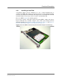
Installing a Hard Disk
A hard-disk adapter card for installation of a 2.5", 9.5mm hard-disk drive is
available from MEN. The adapter is designed in such a way that standard hard disks
can easily be installed. For flexibility the adapter does not include the hard disk
itself but includes all necessary screws to mount a standard hard disk.
Please see MEN’s website for ordering options.
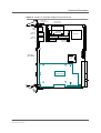
If you want to install a hard disk on the board using MEN’s adapter card, please
keep in mind that the assembly occupies some of the space usually used for
mezzanine modules. See Chapter 1.1 Maps of the Board on page 14 and Figure 11,
Position of Hard-Disk Adapter Card on the Board, on page 35.
Figure 10. A12C (VMEbus-family board) with Hard-Disk Adapter and Hard Disk
MEN Mikro Elektronik GmbH
20SC13-00 E3 - 2004-01-30
34
Functional Description
Figure 11. Position of Hard-Disk Adapter Card on the Board
VMEbus P1 (A12 board family)
Ethernet
10Base-T 1
CompactFlash
card connector
SO-DIMM
DRAM Socket
MPC8245
1
Ethernet
10Base-T 2
Production/Test
Userconfigurable
hex switch
Power Connector
(SC13 family)
Reset Button/LED
RS232
COM1
I/O Connector
Front-panel
mounting screw
Front Panel
Side of Board
CompactPCI J1/J2 (D3 board family)
M1543
ALI
Hard Disk Adapter
IDE Interface
Front-panel
mounting screw
MEN Mikro Elektronik GmbH
20SC13-00 E3 - 2004-01-30
35
Functional Description
2.10
Ethernet Interface
The two Ethernet interfaces of the SC13 support both 10Mbits/s and 100Mbits/s as
well as full-duplex operation and autonegotiation.
!
Note: The unique Ethernet address is set at the factory and should not be changed.
Any attempt to change this address may create node or bus contention and
thereby render the board inoperable. A label on the Ethernet connectors of the
board gives the set Ethernet address.
2.10.1
Connection
Two standard RJ45 connectors with status LEDs are available at the front panel for
connection to 10Base-T or 100Base-TX network environments. It is not necessary
to switch between the two configurations!
The pin assignment corresponds to the Ethernet specification IEEE802.3.
Connector types:
• Modular 8/8-pin mounting jack according to FCC68
• Mating connector:
Modular 8/8-pin plug according to FCC68
Table 7. Pin Assignment and Status LEDs of the 8-pin RJ45 Ethernet 10Base-T/
100Base-T Connectors
Lights up whenever there is
transmit or receive activity
ACT
1
Lights up as soon as the
link is established
(10Base-T or 100Base-T)
LNK
8
1
TX+
2
TX-
3
RX+
4
Shield_R
5
Shield_R
6
RX-
7
Shield_R
8
Shield_R
Table 8. Signal Mnemonics of the Ethernet 10Base-T/100Base-T Connectors
Signal
Function
Shield_R
-
Shield via RC network
RX+/-
in
Differential pair of receive data lines
TX+/-
out
Differential pair of transmit data lines
MEN Mikro Elektronik GmbH
20SC13-00 E3 - 2004-01-30
Direction
36
Functional Description
2.10.2
General
Ethernet is a local-area network (LAN) protocol that uses a bus or star topology and
supports data transfer rates of 100Mbps and more. The Ethernet specification served
as the basis for the IEEE 802.3 standard, which specifies the physical and lower
software layers. Ethernet uses the CSMA/CD access method to handle simultaneous
demands. It is one of the most widely implemented LAN standards.
Ethernet networks provide high-speed data exchange in areas that require
economical connection to a local communication medium carrying bursty traffic at
high-peak data rates.
A classic Ethernet system consists of a backbone cable and connecting hardware
(e.g. transceivers), which links the controllers of the individual stations via
transceiver (transmitter-receiver) cables to this backbone cable and thus permits
communication between the stations.
2.10.3
10Base-T
10Base-T is one of several adaptations of the Ethernet (IEEE 802.3) standard for
Local Area Networks (LANs). The 10Base-T standard (also called Twisted Pair
Ethernet) uses a twisted-pair cable with maximum lengths of 100 meters. The cable
is thinner and more flexible than the coaxial cable used for the 10Base-2 or
10Base-5 standards. Since it is also cheaper, it is the preferable solution for costsensitive applications.
Cables in the 10Base-T system connect with RJ45 connectors. A star topology is
common with 12 or more computers connected directly to a hub or concentrator.
The 10Base-T system operates at 10Mbps and uses baseband transmission methods.
2.10.4
100Base-T
The 100Base-T networking standard supports data transfer rates up to 100Mbps.
100Base-T is actually based on the older Ethernet standard. Because it is 10 times
faster than Ethernet, it is often referred to as Fast Ethernet. Officially, the 100Base-T
standard is IEEE 802.3u.
Like Ethernet, 100Base-T is based on the CSMA/CD LAN access method. There
are several different cabling schemes that can be used with 100Base-T, e.g.
100Base-TX, with two pairs of high-quality twisted-pair wires.
MEN Mikro Elektronik GmbH
20SC13-00 E3 - 2004-01-30
37
Functional Description
2.11
I/O Connector
The board features a 40-pin I/O connector that implements several interfaces:
• Serial port COM2 (compatible with MEN’s SA adapters, see Chapter 2.12 Serial
Ports COM1..COM4 on page 41)
• Serial ports COM3 and COM4 of the MPC8245
• A reset and abort button1
• Two user-configurable LEDs1
• Keyboard/mouse2
The built-in PS2/AT keyboard and PS2 mouse controller of the M1543 is connected to the I/O connector.
• USB port2
Connector types 40-pin connector:
• 40-pin low-profile plug, 2.54mm pitch, for ribbon-cable connection
• Mating connector:
40-pin IDC receptacle, e.g. Elco Series 8290 IDC socket
1
!
2
!
These ports are implemented on the connector, but there are no buttons and LEDs on the
board. Please contact our sales staff if you need any help or extensions to use these
interfaces.
These ports are implemented on the connector but may not be supported through software.
Please contact our sales staff if you need any help or extensions to use these interfaces.
MEN Mikro Elektronik GmbH
20SC13-00 E3 - 2004-01-30
38
Functional Description
Table 9. Pin Assignment of the 40-pin I/O Connector
40
2
1
39
1
40
Reserved1
39
Reserved
38
Reserved
37
Reserved
36
Reserved
35
Reserved
34
Reserved
33
Reserved
32
RXD4
31
Reserved
30
TXD4
29
Reserved
28
RXD3
27
TXD3
26
+5V
25
GND
24
USBP0+
23
USBP0-
22
+5V
21
GND
20
MSDATA
19
MSCLK
18
KBDATA
17
KBCLK
16
LED2
15
LED1
14
ABRTBTN#
13
PWRBTN#
12
+5V
11
GND
10
RI2#
9
DCD2#
8
CTS2#
7
DSR2#
6
RTS2#
5
DTR2#
4
RXD2
3
TXD2
2
+5V
1
GND
Reserved pins on the I/O connector cannot be used but do not impair functionality of the connector.
Table 10. Signal Mnemonics of 40-pin I/O Connector
Button LEDs
Mouse/
Keyboard
Power
Signal
MEN Mikro Elektronik GmbH
20SC13-00 E3 - 2004-01-30
Direction
Function
+5V
-
+5V power supply
GND
-
Digital ground of respective interface
KBDATA
out
Keyboard data
KBCLK
out
Keyboard clock
MSDATA
out
Mouse data
MSCLK
out
Mouse clock
LED1
out
LED1 cathode1
LED2
out
LED2 cathode1
ABRTBTN#
in
Abort button2
PWRBTN#
in
Reset button2
39
Functional Description
USB
MPC8245
COM3/COM4
M1543
COM2
Signal
1
2
Direction
Function
CTS2#
in
Serial port COM2 clear to send
DCD2#
in
Serial port COM2 data carrier detect
DSR2#
in
Serial port COM2 data set ready
DTR2#
out
Serial port COM2 data terminal
ready
RI2#
in
Serial port COM2 ring indicator
RTS2#
out
Serial port COM2 request to send
RXD2
in
Serial port COM2 receive data
TXD2
out
Serial port COM2 transmit data
RXD3
in
Serial port COM3 receive data
(MPC8245)
TXD3
out
Serial port COM3 transmit data
(MPC8245)
RXD4
in
Serial port COM4 receive data
(MPC8245)
TXD4
out
Serial port COM4 transmit data
(MPC8245)
USBP0+, USBP0-
in/out
USB port differential pair
Connect the anode to +5V (pin 12 of 40-pin connector).
Connect the button’s second terminal to GND (pin 11 of 40-pin connector).
2.11.1
Making the Interfaces Available
Of course you can use any interface provided through the 40-pin I/O connector as
needed using ribbon cable and lead it wherever you need it in the system.
However, the easiest way to make the interfaces of the I/O connector available is to
connect the CPU board to MEN’s 6U I/O extension card AD67. This card provides a
convenient 1-slot expansion by all functions of the 40-pin connector. You can use
SA adapters with COM2..COM4 simply by plugging adapters to the AD67.
For ordering information and detailed documentation on AD67 see MEN’s website.
MEN Mikro Elektronik GmbH
20SC13-00 E3 - 2004-01-30
40
Functional Description
2.12
Serial Ports COM1..COM4
The onboard Super I/O controller Ali M1543 provides two high-performance 16550
compatible UARTs with 16-byte send/receive FIFOs and a programmable baud rate
generator. These UARTs are used as COM1 and COM2.
The MPC8245 provides another two UARTs, used as COM3 and COM4.
2.12.1
COM1
COM1 is a standard RS232 interface led to an RJ45 connector at the front panel.
Connector types:
• Modular 8/8-pin mounting jack according to FCC68
• Mating connector:
Modular 8/8-pin plug according to FCC68
Table 11. Pin Assignment of 8-pin RJ45 RS232 Connector (COM1)
1
1
DSR
2
DCD
3
DTR
4
GND
5
RXD
6
TXD
7
CTS
8
RTS
8
2.12.2
COM2..COM4
COM2..COM4 are available via the 40-pin I/O connector. The signal level is fixed
to TTL. This allows flexible line interface configuration using serial interface (SA)
adapters.
COM2..COM4 support the use of MEN’s standard SA adapters. This allows you to
choose from a number of available line interfaces, from RS232 to RS422/RS485 to
TTY, with or without optical isolation.
COM2 is a full-fledged serial interface, while COM3 and COM4 only provide basic
serial lines and have no handshake lines.
For pin assignments of COM2..COM4 please refer to Chapter 2.11 I/O Connector
on page 38.
MEN offers a mounting kit for connection of standard SA adapters (see MEN’s
website).
For compatible adapters and ordering numbers see MEN’s website.
MEN Mikro Elektronik GmbH
20SC13-00 E3 - 2004-01-30
41
Functional Description
2.12.2.1 Installing Standard SA Adapters
You can install SA adapters either through ribbon-cable connection directly on the
40-pin I/O connector, or using an additional I/O extension card, MEN’s AD67.
Please see Chapter 2.11 I/O Connector on page 38 and MEN’s website for more
information. The following description shows how to install SA adapters without
any extension card.
!
Note: MEN gives no warranty on functionality and reliability of the board and SA
adapters used if you install SA adapters in a different way than described in
this manual.
Perform the following steps to install standard SA adapters using MEN’s mounting
kit:
Power-down your system and remove the board from the system.
Remove the front panel screws of the SA adapter.
Use the front panel screw to fasten the SA adapter at the additional SA adapter
front panel.
Plug the prefolded ribbon cable to the 40-pin I/O connector on the board.
Plug the two 10-pin connector of the ribbon cable to the respective SA adapter
connector.
Make sure to always match the pins correctly (pin 1 is marked by a triangle on
the ribbon cable connector).
You can now reinsert the board and the additional front panel into your system.
Make sure to fasten the SA adapter front panel appropriately in your enclosure!
MEN Mikro Elektronik GmbH
20SC13-00 E3 - 2004-01-30
42
Functional Description
2.13
Temperature Sensor
The LM75 temperature sensor is used for temperature management. It continuously
measures the board temperature.
2.14
Real-Time Clock and NVRAM
The board includes the 41T56 SMB real-time clock with integrated NVRAM. A
local GoldCap capacitor supplies the backup voltage.
The 56-byte NVRAM is organized as a 56 bytes x 8 bits SRAM.
2.15
Watchdog
The board uses an SMS24 watchdog, which has three functions:
• Power-On Reset
• Watchdog
• EEPROM (2KB) (see Chapter 2.5.4 EEPROM on page 25)
2.16
User-Defined Hex Switch
The board provides a rotary hex switch for operating system requirements and user
applications. Please refer to the corresponding software manual for their
implementation.
Figure 12. Position of Hex Switch
Ethernet
10Base-T 1
CompactFlash
card connector
SO-DIMM
DRAM Socket
MPC8245
1
Ethernet
10Base-T 2
Userconfigurable
hex switch
ector
mily)
Production/Test
VMEbus P1 (A12 board family)
Reset Button/LED
RS232
COM1
I/O Connector
Front-panel
mounting screw
MEN Mikro Elektronik GmbH
20SC13-00 E3 - 2004-01-30
43
MENMON
3
MENMON
3.1
General
MENMON is an assembly-language debugger with a simple user console interface
and can easily be extended and ported.
MENMON for SC13 also uses some parts of Motorola’s DINK32 and provides
extensions for user interface, configuration, debugging and self test.
Purpose
• Debugging applications without any operating system
• Bootstrapping operating systems
• Hardware testing
Features
• Auto-configuration for PCI devices on the board and devices on secondary PCI
buses
• Interrupt routing of all on-board devices and of all devices on secondary PCI
buses
• SDRAM size detection, reading and checking (Serial Presence Detect Data
Structure)
• Flash programming with password protection of MENMON spaces
• Primary/secondary MENMON
• Subset of Motorola PPCBug system calls implemented
3.2
Console
MENMON for the board can communicate through the COM1 port (available
through the I/O connector).
Additionally, if a P1 graphics PC•MIP module is found on the PCI bus, any console
output will also appear on the VGA display. The same is true if you connect a PS/2
keyboard to the I/O connecter. Characters can then be entered on the RS232 console
and on the PS/2 keyboard.
The default setting of the COM ports is 9600 baud, eight data bits, no parity, one
stop bit.
MEN Mikro Elektronik GmbH
20SC13-00 E3 - 2004-01-30
44
MENMON
3.3
MENMON Memory Map
Figure 13. MENMON Address Mapping
0x 0000 0000
Exception Wrappers
0x 0000 3000
MENMON Parameter String
0x 0000 3200
Unused
0x 0000 4200
VxWorks Bootline
12KB
512 bytes
4KB
256 bytes
0x 0000 4300
Unused
16MB
Download Area for
SERDL
DBOOT
NBOOT
15MB
MENMON relocated code
Global Data
512KB
0x 01F8 0000
MENMON Stack
64KB
0x 01F9 0000
User Program Stack
64KB
MENMON Memory Pool (malloc)
384KB
Runaway Stack
64KB
0x 0100 0000
0x 01F0 0000
0x 01FA 0000
0x 01FF 0000
MEN Mikro Elektronik GmbH
20SC13-00 E3 - 2004-01-30
45
MENMON
3.4
MENMON Start-up
3.4.1
User LEDs
There are two LEDs available on the I/O connector (see Chapter 2.11 I/O Connector
on page 38). The LEDs display the state of the boot like a counter.
!
The exact sequence of the LEDs, i. e. when each LED will light, depends on the
MENMON version. If you have any problems during start-up, please turn to MEN’s
support at [email protected] and give your MENMON version.
3.4.2
Boot Sequence
The assembler part of MENMON initializes the CPU and the host-to-PCI bridge
integrated in the MPC8245 (memory interface), and the monitor will be relocated to
the main memory.
All known devices will be initialized.
The primary MENMON looks for a valid secondary MENMON and starts it unless
the ABORT button is pressed, which is available on the I/O connector. ("Valid"
means the size is between 0x0000 and 0x80000 and the checksum is valid.)
If you press the ABORT button for more than five seconds, the MENMON settings
in the EEPROM are restored with default values.
MENMON checks whether there is a valid "startup" string stored in EEPROM. If
valid, all commands in the "startup" string are executed. (See Chapter 3.4.3
Configuring the MENMON Start-up Procedure on page 46.)
If no startup string was present, MENMON jumps to the operating system
bootstrapper whose address can be configured using the EE-BS command.
The MENMON command line interface will appear if the ESC key is pressed or the
bootstrapper address is set to an invalid address (i. e. 0x0 or 0xFFFFFFFF)
3.4.3
Configuring the MENMON Start-up Procedure
MENMON can be configured to automatically execute commands at start-up, for
example to boot from disk. The EE-STARTUP command can be used to configure
these commands. The EEPROM stores a string (max. 79 characters) that is
comprised of commands that are executed at startup, e.g:
DBOOT 1 FILE=MYBOOT; NBOOT
MENMON performs these commands until one of the commands passes control to a
loaded image.
The "EE-STARTUP -" command can be used to deactivate autoexecution of the
string. When the string is inactive, MENMON calls its BO command at start-up.
MEN Mikro Elektronik GmbH
20SC13-00 E3 - 2004-01-30
46
MENMON
3.4.4
Self Tests
At start-up the monitor runs self tests depending on the current self test level. (OFF,
QUICK or EXTENDED). The MENMON behavior depends on the current stop on
error mode (NO HOLD or HOLD).
Power On Self Test output with self test message mode EXTENDED:
=== PCI ===
MPC107
ALI1543 PCI2ISA
ALI1543 IDE
ALI1543 PMU
Enet 82559 I
Enet 82559 II
M-Mod Bridge
VME Bridge
PC-MIP/PMC Bridge
CPCI Bridge
CPCI slot 2
CPCI slot 3
CPCI slot 4
CPCI slot 5
CPCI slot 6
CPCI slot 7
CPCI slot 8
SO-SIMM SPD
RTC
LM75
HEX-SW
CHECKSUM
3.4.4.1
bus
bus
bus
bus
bus
bus
bus
bus
bus
bus
bus
bus
bus
bus
bus
bus
bus
===
==>
==>
==>
===
==>
===
==>
0x0, dev 0x00
0x0, dev 0x12
0x0, dev 0x1B
0x0, dev 0x1C
0x0, dev 0x17
0x0, dev 0x1A
0x0, dev 0x18
0x0, dev 0x19
0x0, dev 0x1D
0x0, dev 0x1E
0x1, dev 0x0F
0x1, dev 0x0E
0x1, dev 0x0D
0x1, dev 0x0C
0x1, dev 0x0B
0x1, dev 0x0A
0x1, dev 0x09
SMB ===
OK
OK
OK
HEX ===
OK
FLASH ===
OK
==>
==>
==>
==>
==>
==>
==>
==>
==>
==>
==>
==>
==>
==>
==>
==>
==>
OK
OK
OK
OK
OK
OK
OK
NOT
NOT
OK
NOT
NOT
NOT
NOT
NOT
NOT
NOT
PRESENT
PRESENT
PRESENT
PRESENT
PRESENT
PRESENT
PRESENT
PRESENT
PRESENT
Self Tests in Detail
Self tests can be manually started using the command DIAG xxx, e.g. DIAG RTC.
DIAG ALL executes all self tests.
RTC
The RTC test is non-destructive. It writes and compares the RTC NVRAM.
MEN Mikro Elektronik GmbH
20SC13-00 E3 - 2004-01-30
47
MENMON
PCI
This test scans the PCI bus with configuration cycles for PCI devices. This test
checks if all required devices are present. An error is reported if one of the following
devices is missing:
• Integrated host-to-PCI bridge of MPC8245
• ALI1543
• Ethernet I
MENMON also checks for the following optional devices, but the absence of these
devices is not treated as an error:
•
•
•
•
•
Ethernet II
M-Module bridge
VMEbus bridge
CompactPCI bridge
CompactPCI slots
SMB
This test performs read accesses to all on-board SMB devices.
Hex Switch
This test reads and displays the current hex switch position.
MENMON Flash Checksum
This test checks the checksum of the current MENMON (primary/secondary). The
first long word of MENMON contains the size, the second long word contains the
expected checksum. The test computes the checksum by XORing each long word of
MENMON with the next one, except for the first two long words.
ABORT Button
This test checks pressing and releasing of the ABORT button to test port pin GPI 0
of the M1543 (cf. Chapter 4.3 Implementation of M1543 PCI-to-ISA Bridge on
page 79).
The test is not performed during Power On Self Test.
This test does not check the ABORT interrupt.
CPU
This test enters and displays the clock configuration.
The test is not performed during Power On Self Test.
An error is detected for unknown PLL configuration for the installed CPU type.
It also displays the board temperature.
MEN Mikro Elektronik GmbH
20SC13-00 E3 - 2004-01-30
48
MENMON
3.5
MENMON Boot Methods for Client Programs
MENMON supports different methods to load and start client programs like
operating systems or their bootstappers:
• Disk boot
• Network boot
• Execution from Flash.
3.5.1
MENMON BIOS Devices
For disk and network Boot, MENMON supports several device tables. At the lowest
level there is the controller device, an instantation of a controller driver. For
example an IDE controller is a controller device. Each controller device is assigned
a Controller Logical Unit Number (CLUN), to refer to the controller device. The
controller device table is built only at startup of the CPU and is never changed at
runtime.
On the next level there are high-level devices. For example, an IDE or SCSI hard
disk would be called a device by the MENMON BIOS. Each device is assigned a
Device Logical Unit Number (DLUN) that is unique for the controller. The
MENMON device table is built dynamically on request (entries are added by the IOI
or DBOOT command, for example).
The IOI command can be used to display the CLUNs and DLUNs known by
MENMON. IOIN just displays the currently known devices while IOI will search
for devices behind each controller.
Example
MenMon> IOI
====== [ Controller Dev Table ] =========
CLUN Driver
param1
param2
0x00 IDE
0x000001F0 0x000003F6
0x01 IDE
0x00000170 0x00000376
0x02 Etherboot
0xFE002200 0x8A100000
0x03 Etherboot
0xFE002240 0x8A140000
====== [ Device Table ] =========
CLUN DLUN Device
Scanning for devices on IDE bus (CLUN=0x00)...
0x00 0x00 SanDisk SDP3B-8
0x01FEFC90
param3
0x00000000
0x00000000
0x00001700
0x00001A00
Type
Handle
0x00000000
0x00000000
0x00000000
0x00000000
Handle
IDE HD
Scanning for devices on IDE bus (CLUN=0x01)...
Autoscan not possible on CLUN=0x02
Autoscan not possible on CLUN=0x03
MEN Mikro Elektronik GmbH
20SC13-00 E3 - 2004-01-30
49
MENMON
3.5.1.1
Controller Devices (CLUNs)
On startup, MENMON searches for all known onboard controllers (CLUN
0x00..0x0F) and for any other PCI device that is supported by the MENMON
drivers. If additional controllers are found on the PCI bus, they receive CLUNs ≥
0x10.
Table 12. MENMON - Assignment for Board Controller Devices
CLUN
Controller
0x00
Primary IDE controller in ALI
0x01
Secondary IDE controller in ALI
0x02
First onboard Ethernet interface
0x03
Second onboard Ethernet interface
0x10..0FE Any other controller found that is supported by the MENMON drivers
3.5.1.2
High Level Devices (DLUNs)
Depending on the bus type, the DLUN is assigned differently:
Device LUNs (8-bit value)
For IDE devices:
7..0
0 = Master, 1 = Slave
For SCSI devices:
7..4
3..0
SCSI ID
SCSI LUN (normally 0)
Example: A SCSI hard disk with ID 6 would have a DLUN of 0x60.
MEN Mikro Elektronik GmbH
20SC13-00 E3 - 2004-01-30
50
MENMON
3.5.2
Disk Boot
Disk boot supports the following:
• Boot from any disk-like device: SCSI hard and floppy disks1, IDE hard disks or
CompactFlash.
• Supports PReP and DOS disk partitions as well as unpartitioned media.
• Supported file formats: RAW, ELF, PReP and PPCBOOT images.
To be able to boot from disk media, each medium must be prepared in the following
way:
Partitions
Hard disks can have a partition table. MENMON supports the four partition entries
in the first sector of the medium. The partition type must be either DOS (Type
0x01, 0x04, 0x06) or PReP (Type 0x41).
Figure 14. MENMON—Layout of the 0x41-Type Partition (PReP)
0
0
PC Compatibility Block
512
Entry Point Offset (LE)
516
Load Image Length (LE)
Load Image
Flag Field
520
OS_ID
521
522
Partition Name
554
Reserved1
OS-Specific Field
(optional)
Entry Point (Code
Aligned)
1023
Code Section of the Load Image
Reserved2
RBA_Count x 512
File System
With DOS-formatted partitions (or unpartitioned media) the file system must be a
DOS FAT file system (12-bit or 16-bit FAT entries).
PReP (Type 0x41) partitions have no file system, the entire partition is viewed as a
single file (no file name is required).PReP partitions can contain either a PReP file
(as in the above figure) or a PPCBOOT image.
1
The board supports SCSI devices only through use of a PC•MIP module!
MEN Mikro Elektronik GmbH
20SC13-00 E3 - 2004-01-30
51
MENMON
3.5.2.1
DBOOT Algorithm
The DBOOT command tries to find a bootable partition or file on any disk. If no
parameters are specified, DBOOT will search for devices behind each known
CLUN. On each disk found, it will check if there is a partition table on it, and
checks with each partition if it is bootable or not.
Any PReP partition found is assumed to be bootable.
For DOS partitions, DBOOT searches if the DOS file system contains the specified
file. The file name to be searched for can be configured in the EEPROM using the
EE-BOOTFILE (or EE-VXBLINE) command. Only the file-name part of that name
is used (e. g. if you configure EE-BOOTFILE /ata0/vxworks, then DBOOT looks
for "vxworks").
The file name can also be passed to the command line to DBOOT (e. g. DBOOT
file=myboot). The boot file must be in the root directory of the hard disk.
If no file name is configured in EEPROM and no file-name argument is passed to
DBOOT, the filename defaults to "BOOTFILE".
3.5.2.2
Loading the Boot File
Once a bootable device/partition has been found, the DBOOT command starts to
load the file. Regardless of the file format, the entire boot file will be loaded to
MENMON’s download area (0x01000000). (This address can be overridden
using the LOAD parameter.) The load address must not be between 0x01F00000
and 0x01FFFFFF.
MEN Mikro Elektronik GmbH
20SC13-00 E3 - 2004-01-30
52
MENMON
3.5.2.3
Starting the Loaded Program
RAW and PReP files will be executed at the load address.
For RAW files, the entry point, relative to the load address, can be specified through
the START parameter to the DBOOT command. (The default start offset is 0, i.e. the
program execution begins at the load address.)
PReP files begin with a header, which contains the entry point of the program. The
START parameter will be ignored in this case.
ELF files will not be executed at the load address. Instead MENMON analyzes the
ELF program header and sections, and the program sections will be relocated as
specified in the ELF file. Here, the relocation address may be any address in RAM
except the runaway stack and the load image itself. Only the physical address
entries in the ELF program headers are used, virtual addresses are treated as
physical addresses if the physical address entry is 0xFFFFFFFF.
Client Program Calling Conventions (for ELF, RAW and PReP files)
•
•
•
•
•
•
•
•
Interrupts are disabled (MSR.EE is cleared).
CPU is in Big Endian Mode.
MMU is enabled. BATs are set up.
Instruction Cache is enabled.
R1 is set to the top of runaway stack - 512 bytes.
R3 is set to 0 (no residual data available).
R4 is set to the image loading address. (Not the relocation address!)
R5..R7 are cleared.
MEN Mikro Elektronik GmbH
20SC13-00 E3 - 2004-01-30
53
MENMON
3.5.2.4
Syntax
Using the DBOOT Command
DBOOT [clun] [dlun] [PART=part] [FILE=file] [LOAD=addr]
[START=off] [HALT=n] [KERPAR=p1=x p2=y]
Parameters clun
Controller logical unit. If missing, DBOOT loops through
all known controllers.
dlun
Device logical unit. If missing, DBOOT automatically
searches for devices.
PART
Partition number [1..4]. If missing, DBOOT loops through
all partitions.
FILE
File name. Used when booting from a DOS FAT file system. The file must be present in the file system’s root
directory. If FILE is missing, the name "BOOTFILE" is
used. The file name is ignored when booting from Type41
partitions.
LOAD
Specifies the load address. This is the address where the
entire image of the file is first loaded, regardless of the
file format. If not specified, the download area is used.
START
Specifies the entry point of the loaded program relative to
its load address. Only used for RAW files. If START is not
present, the entry point is equal to the load address.
HALT
If this parameter is ’1‘, MENMON is called again when
the boot file was loaded. If this parameter is ’2‘, MENMON is called when the load image was relocated, right
after the first instruction of the program was executed.
KERPAR Parameters to add to kernel command line (only used
when booting PPCBOOT image)
Examples
• Load PReP boot from second partition of CompactFlash:
DBOOT 0 0 PART=2
• Load file MYBOOT from IDE hard disk on secondary IDE channel, master:
DBOOT 1 1 FILE=MYBOOT
• Try to find a bootable device on secondary IDE:
DBOOT 1
• Boot Linux from PPCBOOT image and pass kernel parameters:
DBOOT FILE=busybox.img KERPAR='root=ramfs console=ttyS0,9600'
MEN Mikro Elektronik GmbH
20SC13-00 E3 - 2004-01-30
54
MENMON
• Boot VxWorks from ATA:
MenMon> ee-vxbline
'.' = clear field;
'-' = go to previous field;
^D = quit
boot device
:ata=0,0
processor number
:0
host name
:host
file name
:/ata0/vxworks
inet on ethernet (e) :192.1.1.28
inet on backplane (b) :
host inet (h)
:192.1.1.22
gateway inet (g)
:
user (u)
:
ftp password (pw) (blank = use rsh):
flags (f)
:0x0
target name (tn)
:
startup script (s)
:
other (o)
:
Updating EEPROM..
MenMon> DBOOT 0
Hints
• Use the LS command to display the partition table and files on the device.
• In case of problems you can try to read raw sectors from disk using the DSKRD
command.
• Use the EE-STARTUP command to perform the DBOOT command automatically at startup.
MEN Mikro Elektronik GmbH
20SC13-00 E3 - 2004-01-30
55
MENMON
3.5.3
Network Boot
Network boot supports the following:
• Boot a file using BOOTP and TFTP protocols via Ethernet.
• Boot a file using TFTP only (without BOOTP).
• Supported file formats: RAW, ELF and PReP.
This boot method requires a host computer running the TCP/IP daemons tftpd and
optionally bootp. If you intend to boot via BOOTP, the host computer must also set
up a table (usually called bootptab) containing an entry for each target system to be
booted.
An entry in bootptab for the board could look like this:
mysystem:sm=255.255.255.0:\
hd=/usr/TFTPBOOT:\
bs:ht=ether:vm=rfc1048:\
ha=00c03a080003:\
ip=192.1.1.25:\
bf=mybootfile
At start-up, MENMON searches for the first available (and supported) Ethernet
controller in the system. When the NBOOT command is issued, MENMON uses
that controller (unless the CLUN parameter is specified) to send its BOOTP
broadcast. The BOOTP server will respond with a packet containing the target’s IP
address, home directory and boot file. Now MENMON will fetch the specified file
using the TFTP protocol.
The number of tries to get the BOOTP parameters or to load a file via TFTP is
configurable in EEPROM:
• EE-NTRY
rty
BOOTP/TFTP retries
-1 default
0 forever
1..127
You can also boot through TFTP only. In this case, you must configure some
parameters in the EEPROM. These parameters can be configured using either EEVXBLINE or the EE-NETxxx parameters.
Example of Booting a Specified File
MenMon> ee-netip 192.1.1.28
MenMon> ee-nethost 192.1.1.22
MenMon> ee-bootfile /FWARE/PPC/MENMON/PORTS/A12/BIN/menmon.rom
MenMon> nboot tftp
Probing...[Tulip] Tulip 00:C0:3A:08:00:17 at membase = 0xF0001000
Performing ethernet autonegotiation (V2)...100BaseTx FD
Etherboot/32 version 4.2.5b for [Tulip]
My IP 192.1.1.28, Netmask=0xFFFFFF00 Server IP 192.1.1.22, GW IP
0.0.0.0
Loading /FWARE/PPC/MENMON/PORTS/A12/BIN/menmon.rom...
to 0x01000000
352 kB
Loaded 0x000580DC bytes
Starting RAW-file
MEN Mikro Elektronik GmbH
20SC13-00 E3 - 2004-01-30
56
MENMON
As with the DBOOT command, the entire boot file will be loaded to MENMON’s
download area if not otherwise specified. Once the boot file has been loaded, the
file is interpreted, relocated and executed in the same way as described for the
DBOOT command. (See Chapter 3.5.2.3 Starting the Loaded Program on page 53.)
Client Program Calling Conventions
See Chapter Client Program Calling Conventions (for ELF, RAW and PReP files)
on page 53.
3.5.3.1
Syntax
Using the NBOOT Command
NBOOT [BOOTP=??] [TFTP=??] [CLUN=clun] [FILE=file]
[LOAD=addr] [START=addr] [HALT=n] [KERPAR=p1=x p2=y]
Parameters BOOTP
(Default) Obtain IP address from BOOTP server. Then
boot via TFTP.
TFTP
Use TFTP method only. Use parameters specified by EENETxx commands.
CLUN
Specifies the controller that should be used for network
boot. If CLUN is not present, the first available controller
is used.
FILE
File name to be sent within the BOOTP request. If FILE is
not present, the file name must be provided by the
BOOTP server (using the "bf" tag). A file name from the
BOOTP server always takes precedence.
LOAD
See Chapter 3.5.2.4 Using the DBOOT Command on
page 54
START
See Chapter 3.5.2.4 Using the DBOOT Command on
page 54
HALT
See Chapter 3.5.2.4 Using the DBOOT Command on
page 54
KERPAR See Chapter 3.5.2.4 Using the DBOOT Command on
page 54
Note: To boot from the second Ethernet interface of the CPU board, use NBOOT
CLUN=3 <opts>.
MEN Mikro Elektronik GmbH
20SC13-00 E3 - 2004-01-30
57
MENMON
3.6
Updating Flash Devices
MENMON provides the possibility of updating Flash and disk devices on the board
via the serial console interface or via Ethernet.
3.6.1
Download via Serial Interface
In order to program Flash or disk devices, you need to send a file from a host
computer to the target. On the host computer, you need a terminal emulation
program such as HyperTerm or Minicom.
The download file name extension determines the destination device and the offset
within that device. For example, a file named myfile.f00 will be programmed into
Flash sector 0.
Table 13. MENMON—Download Destination Devices
Device Abbreviation
1
Flash Device
Sector Size
F
Flash
See Table 14, MENMON—
Flash Sectors, on page 59
E
Serial EEPROM1
1 byte
D
SDRAM
2 bytes
C
IDE (CompactFlash)
512 bytes
S
SCSI ID0
Sector size from drive
If you want to program the EEPROM and use the file extension to specify the start address,
note that the highest start address you can state is 0x63 (with extension .E99).
Two special extensions are available for MENMON update:
• xxx.PMM
• xxx.SMM
is an alias for .F16 and updates the primary MENMON.
is an alias for .F24 and updates the secondary MENMON.
When a file is larger than one sector, the following sector of the device will also be
programmed.
The update file is transferred to DRAM before being programmed to Flash. The
DRAM of the board must therefore be large enough for the entire download file.
The update file may be max. 1MB (optional 15MB, if equipped with 16MB Flash).
MEN Mikro Elektronik GmbH
20SC13-00 E3 - 2004-01-30
58
MENMON
Table 14. MENMON—Flash Sectors
Flash Sector
Address
Flash Sector
Address
0
0x000000
18
0x120000
1
0x010000
19
0x130000
2
0x020000
20
0x140000
3
0x030000
21
0x150000
4
0x040000
22
0x160000
5
0x050000
23
0x170000
6
0x060000
24
0x180000
7
0x070000
25
0x190000
8
0x080000
26
0x1A0000
9
0x090000
27
0x1B0000
10
0x0A0000
28
0x1C0000
11
0x0B0000
29
0x1D0000
12
0x0C0000
30
0x1E0000
13
0x0D0000
31
0x1F0000
14
0x0E0000
32
0x1F8000
15
0x0F0000
33
0x1FA000
16
0x100000
34
0x1FC000
17
0x110000
3.6.2
Performing the Download
You must connect your host to board's COM1 interface.
Before you start the download, change the MENMON console baudrate to 115,200
baud (enter EE-BAUD 115200 and reset board).
To start download enter SERDL in the MENMON command line. You must specifiy
a password if you want to update the primary MENMON, secondary MENMON or
disk devices:
• SERDL PMENMON for primary MENMON
• SERDL MENMON for secondary MENMON
• SERDL DISK
for disk devices
MEN Mikro Elektronik GmbH
20SC13-00 E3 - 2004-01-30
59
MENMON
3.6.3
Update from Disk or Network
It is also possible to program Flash with a file from a disk or network:
Load the file into memory:
DBOOT HALT=1
or
NBOOT HALT=1
Program the Flash (in this case OS bootstrapper):
PFLASH F 0 100000
This programs the first Mbyte of Flash.
MEN Mikro Elektronik GmbH
20SC13-00 E3 - 2004-01-30
60
MENMON
3.7
MENMON User Interface
3.7.1
Command Line Editing
MENMON provides a rudimentary command line editor:
<CTRL> <H>
Backspace and delete previous character
<CTRL> <X>
Delete whole line
<CTRL> <A>
Retrieve last line
3.7.2
Numerical Arguments
Most MENMON commands require one or more arguments. Numerical arguments
may be numbers or simple expressions:
<num>
num is interpreted as a hexadecimal value
$<num>
Same as above
#<num>
num is interpreted as a decimal value
%<num>
num is interpreted as a binary value
.<REG>
Use the value of register <REG>
These arguments can be combined using the arithmetic operators "+" and "-".
Example:1
MenMon> D 10000
1
Some of the addresses used in our examples may not be suitable for your board’s address
mapping. If you want to try out MENMON’s functions, please compare the example
addresses with your mapping first!
MEN Mikro Elektronik GmbH
20SC13-00 E3 - 2004-01-30
Dumps address 0x10000
61
MENMON
3.7.3
MENMON Command Overview
Table 15. MENMON Command Overview
Command
H
Print help
IOI
Scan for BIOS devices
NBOOT [<opts>]
Boot from network
DEC21MEDIA <clun> <med>
Select Ethernet medium
DBOOT [<clun>] [<dlun>] [<opts>]
Boot from disk
RBOOT [<opts>]
Boot from shared RAM
LS <clun> <dlun> [<opts>]
List files/partitions on device
DSKRD <args>
Read blocks from RAW disk
DSKWR <args>
Write blocks to RAW disk
BIOS_DBG <mask>
Set MMBIOS debug level
I [<D>]
List board information
EEPROSPEED <clun> <med>
Select Ethernet Speed
EE[-xxx] [<arg>]
Serial EEPROM commands
DIAG [<arg>]
System diagnosis
RTC[-xxx] [<arg>]
Real time clock commands
WDOG[-xxx] [<arg>]
Watchdog (SMS24) commands
RST
Reset board
CHAM-xxx
Chameleon FPGA commands
SERDL [<passwd>]
Update Flash using YModem protocol
NDL [<opts>]
Update Flash from network
ERASE <D> [<O>] [<S>]
Erase Flash sectors
PFLASH <D> <O> <S> [<A>]
Program Flash
AS <addr> [<cnt>]
Assemble memory
DI [<addr>] [<cnt>]
Disassemble memory
GO [<addr>]
Jump to user program
S[RFO-] [<addr>]
Single step
BO [<addr>] [<opts>]
Call OS bootstrapper
B[DC#] [<addr>]
Set/display/clear breakpoints
.C[RFM] name
CPU User Register Change
.[RFM?] [name]
CPU User Register Display
ACT [<addr>] [<size>]
Execute a HWACT script
C[BWLLN#] <addr> [<val>]
Change memory
D [<addr>] [<cnt>]
Dump memory
FI <from> <to> <val>
Fill memory (byte)
MC <adr1> <adr2> <cnt>
Compare memory
MEN Mikro Elektronik GmbH
20SC13-00 E3 - 2004-01-30
Description
62
MENMON
Command
Description
MO <from> <to> <cnt>
Move (copy) memory
MS <from> <to> <val>
Search pattern in memory
MT[BWLFD] <from> <to>
Memory test
PCID[+] <dev> [<bus>] [<func>]
PCI config register dump
PCIC <dev> <addr> [<bus>] [<func>]
PCI config register change
PCIR
List PCI resources
PCI-VPD[-] <devNo> [<busNo>] [<capId>] PCI Vital Product Data dump
PCI
MEN Mikro Elektronik GmbH
20SC13-00 E3 - 2004-01-30
PCI probe
63
MENMON
3.8
Board Setup
3.8.1
ALI 1543
The PCI-to-ISA southbridge contains preconfigured and unconfigured Plug and
Play devices.
MENMON enables and configures the following devices:
•
•
•
•
•
•
•
•
COM1
COM2
Keyboard
Mouse
Primary/secondary IDE
DMA controller
PMU
SMB controller
MENMON disables the following devices:
• USB
3.8.2
PCI Auto-Configuration
MENMON maps all detected local PCI devices to PCI memory and PCI I/O space.
PCI bus masters are enabled. PCI bus interrupts are routed and configured in
configuration space.
The cacheline size and latency timer registers of all PCI devices are initialized:
PCI Latency Timer = 0x40 = 1.94µs
MEN Mikro Elektronik GmbH
20SC13-00 E3 - 2004-01-30
64
MENMON
The information command I displays the current PCI configuration:
Figure 15. MENMON—Example PCI Configuration
*PCI
busNo
=====
0x 0
0x 0
0x 0
0x 0
0x 0
0x 0
0x 0
0x 0
devNo
=====
0x 0
0x12
0x17
0x18
0x1A
0x1B
0x1C
0x1E
funcNo
======
0x 0
0x 0
0x 0
0x 0
0x 0
0x 0
0x 0
0x 0
DEV ID
======
0x0003
0x1533
0x1209
0x410C
0x1209
0x5229
0x7101
0x0022
VEN ID
======
0x1057
0x10B9
0x8086
0x1172
0x8086
0x10B9
0x10B9
0x1011
NUMBER OF MAPPED PCI BUSSES => 1
PCI IO:
START => FE002200
END
=> FE00EFFF
ALLOC => FE003000
PCI MEMORY:
START => 8A100000
END
=> 9FFFFFFF
ALLOC => 8A200000
PCI INT ROUTING:
INTA =>
7
INTB => 10
INTC => 11
INTD => 11
PCI BRIDGES:
PrimBus DevNo SecBus
------- ----- -----0x 0 0x1E
0x 1
There are two commands to control some features on the PCI bus.
• EE-PCI-STGATH controls PCI store gathering of CPU->PCI cycles.
• EE-PCI-SPECRD controls read prefetching of external master accesses to
the system memory.
There are several commands available to show and modify PCI configuration:
• PCI
•
•
•
•
PCIR
PCID
PCIC
PCI-VPD
MEN Mikro Elektronik GmbH
20SC13-00 E3 - 2004-01-30
scans the entire bus hierarchy and displays the device and vendor ID
of each device found.
shows the allocated PCI I/O and memory resources for each device.
shows the entire PCI configuration space of the specified device.
allows you to change the values of any PCI config space register.
shows the "vital product data" on devices that support it.
65
MENMON
3.8.3
SDRAM DIMM Configuration
The configuration EEPROM will be read over the System Managment Bus. The
monitor software checks the configuration data during boot. The SDRAM controller
is set up according to the information found in the serial presence detect (SPD)
EEPROM. If no valid SPD can be found, defaults are used.
A bad SPD checksum is tolerated as long as the rest appears reasonable.
3.8.4
Watchdog Configuration
By default, the board watchdog is disabled.
The watchdog can be enabled through WDOG-TOUT <ms> where <ms> specifies
the watchdog timeout in milliseconds. Possible values are 0 (disable watchdog),
800, 1600, 3200, and 6400.
Once the watchdog is enabled, it must be served by toggling the ALI GPO22 pin. If
the software fails to toggle this pin in time, the CPU is reset.
MENMON automatically and continuously serves the watchdog until the operating
system is started.
3.8.5
Hex Switch
The hex switch is completely user-configurable. With MENMON it has only one
function: at hex position "0" or "8" there will be a delay after each initialization step,
so that the boot procedure is slowed down. This function is provided for diagnostic
purposes. For normal operation of the board, you should set the hex switch to a
position between "1" and "F".
If the hex switch is set to 8 and F, the console can be redirected to a P10 PC•MIP or
AD45 adapter. See Chapter 3.2 Console on page 44.
Table 16. Hex-Switch Settings
Setting
0
User-defined, but delay after each initialization step
1..F
User-defined, no additional delay during boot
MEN Mikro Elektronik GmbH
20SC13-00 E3 - 2004-01-30
Description
66
MENMON
3.9
MENMON System Calls
This chapter describes the MENMON System Call handler, which allows system
calls from user programs. MENMON implements a small subset of the system calls
implemented in Motorola’s PPCBug. The implemented system calls are binarycompatible with PPCBug.
The system calls can be used to access selected functional routines contained within
the debugger, including input and output routines. The System Call handler may
also be used to transfer control to the debugger at the end of a user program.
3.9.1
Invoking System Calls
The System Call handler is accessible through the SC (system call) instruction, with
exception vector 0x00C00 (System Call Exception). To invoke a system call from
a user program, insert the following code into the source program. The code
corresponding to the particular system routine is specified in register R10.
Parameters are passed and returned in registers R3 to Rn, where n is less than10.
ADDI R10,R0,$XXXX
SC
$XXXX is the 16-bit code for the system call routine, and SC is the system call
instruction (system call to the debugger). Register R10 is set to 0x0000XXXX.
MEN Mikro Elektronik GmbH
20SC13-00 E3 - 2004-01-30
67
MENMON
3.9.2
System Calls
3.9.2.1
BRD_ID
Name
BRD_ID — Return pointer to board ID packet
Code
$0070
Description
This routine returns a pointer in R03 to the board identification
packet. The packet is built at initialization time.
The format of the board identification packet is shown below.
MENMON only implements some fields of the original PPCBug
system call.
Table 17. MENMON—System Calls—BRD_ID Fields
31
16 15
0x00
Eye Catcher
0x04
Reserved
0x08
Packet Size
87
0
Reserved
0x0C
Reserved
0x10
Reserved
0x14
Entry
Conditions
24 23
CLUN
DLUN
0x18
Reserved
0x1C
Reserved
Eye Catcher
Word containing ASCII string "BDID"
Packet Size
Half-word containing the size of the packet
CLUN
Logical Unit Number for the boot device controller
DLUN
Logical Unit Number for the boot device
-
Exit Conditions R03: Address
different from (word)
Entry
Starting address of ID packet
Note: CLUN and DLUN are initialized according to the device that was last booted
(for example, DBOOT or NBOOT command).
MEN Mikro Elektronik GmbH
20SC13-00 E3 - 2004-01-30
68
MENMON
3.9.2.2
OUT_CHR
Name
OUT_CHR — Output character routine
Code
$0020
Description
This routine outputs a character to the default output port.
Entry
Conditions
R03: Bits 7
through 0
Character (byte)
Exit Conditions Character is sent to the default I/O port.
different from
Entry
3.9.2.3
IN_CHR
Name
IN_CHR — Input character routine
Code
$0000
Description
IN_CHR reads a character from the default input port. The character is returned in the LSB of R03.
Entry
Conditions
-
Exit Conditions R03: Bits 7 through 0 contain the character returned
different from
R03: Bits 31 through 8 are zero
Entry
3.9.2.4
IN_STAT
Name
IN_STAT — Input serial port status routine
Code
$0001
Description
IN_STAT is used to see if there are characters in the default
input port buffer. R03 is set to indicate the result of the operation.
Entry
Conditions
No arguments required
Exit Conditions R03: Bit 3 (ne) = 1; Bit 2 (eq) = 0 if the receiver buffer is not
different from empty.
Entry
R03: Bit 3 (ne) = 0; Bit 2 (eq) = 1 if the receiver buffer is empty.
MEN Mikro Elektronik GmbH
20SC13-00 E3 - 2004-01-30
69
MENMON
3.9.2.5
RTC_RD
Name
RTC_RD — Read the RTC registers
Code
$0053
Description
RTC_RD is used to read the Real-Time Clock registers. The
data returned is in packed BCD.
The order of the data in the buffer is:
Table 18. MENMON—System Calls—RTC_RD Buffer Data
YY
MM
DD
dd
H
M
0
Buffer
+ eight bytes
Begin buffer
Entry
Conditions
S
YY
Year (2 nibbles packed BCD )
MM
Month (2 nibbles packed BCD) (1..12)
DD
Day of month (2 nibbles packed BCD) (1..31)
dd
Always 0
H
Hour (2 nibbles packed BCD) (0..23)
M
Minutes (2 nibbles packed BCD) (0..59)
S
Seconds (2 nibbles packed BCD) (0..59)
R03: Buffer address where RTC data is to be returned
Exit Conditions Buffer now contains date and time in packed BCD format.
different from
Entry
3.9.2.6
Name
DSK_RD — Disk read routine
Code
$0010
Description
This routine is used to read blocks of data from the specified
disk device. Information about the data transfer is passed in a
command packet which has been built somewhere in memory.
(The user program must first manually prepare the packet.) The
address of the packet is passed as an argument to the routine.
The command packet is eight half-words in length and is
arranged as follows:
MEN Mikro Elektronik GmbH
20SC13-00 E3 - 2004-01-30
DSK_RD
70
MENMON
Table 19. MENMON—System Calls—DSK_RD Fields
15
87
0x00
CLUN
0x02
DLUN
Status Half-Word
0x04
0x06
Most Significant Half-Word
Memory Address
Least Significant Half-Word
0x08
0x0A
0
Most Significant Half-Word
Block Number (Disk)
Least Significant Half-Word
0x0C
0x0E
Number of Blocks
Flag Byte
Address Modifier
CLUN
Logical Unit Number (LUN) of controller to use
DLUN
Logical Unit Number (LUN) of device to use
Status
This status half-word reflects the result of the
operation. It is zero if the command completed
without errors.
Memory
Address
Address of buffer in memory. Data is written
starting at this address.
Block Number
For disk devices, this is the block number where
the transfer starts. Data is read starting at this
block.
Number of
Blocks
The number of blocks to read from the disk. For
streaming tape devices, the actual number of
blocks transferred is returned in this field.
Flag Byte
Not implemented by MENMON
Address Modi- Not used
fier
Entry
Conditions
R03: 32-bit address of command packet
Exit Conditions Status half-word of command packet is updated. Data is written
different from into memory.
Entry
R03: Bit 3 (ne) = 1; Bit 2 (eq) = 0 if errors.
R03: Bit 3 (ne) = 0; Bit 2 (eq) = 1 if no errors.
Note: MENMON’s internal status codes are returned in Status.
MEN Mikro Elektronik GmbH
20SC13-00 E3 - 2004-01-30
71
MENMON
3.10
VxWorks Bootline
MENMON passes a string to the client program that confirms to the standard
VxWorks bootline. This string is copied to a fixed address before the client program
is called.
MENMON stores the VxWorks bootline in the serial EEPROM. MENMON
command EE-VXBLINE allows you to change the bootline interactively (same
behavior as VxWorks bootChange() routine).
There are alternative commands to modify only specific parameters within the
bootline.
The parameters in the bootline are used both by MENMON and by operating system
bootstrappers.
The address of the bootline string is 0x4200 on all PowerPC platforms and has
space for 256 characters.
The bootline has the following form:
bootdev(unitnum,procnum)hostname:filename e=# b=# h=# g=# u=userid
pw=passwd f=#
tn=targetname s=startupscript o=other
The bootline is a null-terminated ASCII string. Example:
enp(0,0)host:/usr/wpwr/target/config/mz7122/vxWorks e=90.0.0.2
b=91.0.0.2 h=100.0.0.4
g=90.0.0.3 u=bob pw=realtime f=2 tn=target
s=host:/usr/bob/startup o=any_string
MEN Mikro Elektronik GmbH
20SC13-00 E3 - 2004-01-30
72
MENMON
Table 20. MENMON—VxWorks Bootline—List of Parameters and their Usage
Parameter
boot device + unit
number
Description
Special
Command
Device name of boot device
Used by
MENMON
No
processor number
No
host name
Name of host to boot from
file name
File name of file to be booted
EE-BOOTFILE Yes, for NBOOT
and DBOOT
inet on ethernet (e=)
IP address and optional subnet mask
of this machine on Ethernet (e. g.
192.1.1.28:ffffff00)
EE-NETIP
inet on backplane (b=)
IP address on backplane
host inet (h=)
IP address of host to boot from
EE-NETHOST Yes, for NBOOT
gateway inet (g=)
IP address of gateway
EE-NETGW
user (u=)
User name
No
ftp password (pw=)
Password
No
flags (f=)
Flags for VxWorks
No
target name (tn=)
Name of this machine
EE-NETNAME No
startup script (s=)
Startup script for VxWorks
EE-KERPAR
other (o=)
Other devices to initialize in VxWorks
MEN Mikro Elektronik GmbH
20SC13-00 E3 - 2004-01-30
No
Yes, for NBOOT
No
Yes, for NBOOT
Yes, when booting
PPCBOOT images
containing a Linux
kernel
No
73
MENMON
3.10.1
Additional MENMON Parameters
Client programs often need to query certain parameters which are already set up or
detected by MENMON. In the past, client programs had to read the EEPROM or
access some registers directly in order to get these parameters.
The new method allows MENMON to pass certain parameters to the client program.
These parameters are stored in an separate ASCII string. The advantages lie in
common access to these parameters over the range of PPC boards and saving time to
boot.
The address of the parameter string is 0x3000 on all PowerPC platforms and has
space for 512 characters.
Table 21. MENMON—Common Parameters Passed by All MENMONs
Parameter
Description
MPAR
Magic word at beginning of string
brd=name
Product name of the board, e. g. SC13a or SC13b
brdrev=xx.yy.zz
Board revision
brdmod=xx
Board model
sernbr=xxxx
Serial number (decimal)
cbr=baud
Console baud rate in bits/s (decimal)
cons=dev
Selected console as an ASCII string (“COM1” or “P10” or
"VGA", if both a graphics module and a PS/2 keyboard
were found)
mem0=size
Size of main memory in KB (decimal)
cpu=name
CPU type (MPC8240, MPC8245)
cpuclk=f
CPU frequency in MHz (decimal)
memclk=f
Memory bus frequency in MHz (decimal)
vmeirqenb=mask
Enabled interrupt levels as defined by EE-VME-IRQ, not
used
clun=num
Controller logical unit number of the boot device when
booted over NBOOT or DBOOT
dlun=num
Device logical unit number of the boot device when booted
over NBOOT or DBOOT
Example
00003000:
00003010:
00003020:
00003030:
00003040:
00003050:
00003060:
00003070:
00003080:
MEN Mikro Elektronik GmbH
20SC13-00 E3 - 2004-01-30
4D504152
64726576
646D6F64
20636272
3D434F4D
20637075
636C6B3D
30302076
636C756E
20627264
3D30302E
3D303020
3D313135
31206D65
3D4D5043
32353020
6D656972
3D303220
3D413031
30302E30
7365726E
32303020
6D303D36
38323430
6D656D63
71656E62
646C756E
32206272
30206272
62723D36
636F6E73
35353336
20637075
6C6B3D31
3D464500
3D303000
MPAR brd=A012 br
drev=00.00.00 br
dmod=00 sernbr=6
cbr=115200 cons
=COM1 mem0=65536
cpu=MPC8245 cpu
clk=250 memclk=1
00 vmeirqenb=FE.
clun=02 dlun=00.
74
Organization of the Board
4
Organization of the Board
To install software on the board or to develop low-level software it is essential to be
familiar with the board’s address and interrupt organization.
4.1
Memory Mappings
The memory mapping of the board complies with the PowerPC CHRP (Common
Hardware Reference Platform) Specification. The integrated host-to-PCI bridge is
set to map B to support this mapping.
4.1.1
Processor View of the Memory Map
Table 22. Memory Map—Processor View
CPU Address Range
Size
Description
0x 0000 0000..0FFF FFFF
1GB
DRAM
0x 1000 0000..7FFF FFFF
1.8GB
Reserved
0x 8000 0000..FCFF FFFF
2GB-48MB
PCI Memory Space
0x FD00 0000..FDFF FFFF
16MB
PCI ISA Memory Space
0x FE00 0000..FE00 FFFF
64KB
PCI ISA I/O Space
0x FE80 0000..FEBF FFFF
4MB
PCI I/O Space (not used)
0x FEC0 0000..FEDF FFFF
2MB
PCI Config Addr. Reg.
0x FEE0 0000..FEEF FFFF
1MB
PCI Config Data. Reg.
0x FEF0 0000..FEFF FFFF
1MB
PCI IACK Space
0x FFE0 0000..FFFF FFFF
2MB
Boot Flash (8-bit)
Table 23. Address Mapping for PCI
Address Range
Size
Description
PCI Memory Space (addresses as seen on PCI bus)
0x 8000 0000..87FF FFFF
M-Module bridge
0x 8800 0000..89FF FFFF
0x 8A00 0000..8A0F FFFF
MPC8245 Embedded utility
block
0x 8B00 0000..9FFF FFFF
Available for PCI auto-configuration
PCI I/O Space (addresses as seen on PCI bus)
0x 0000..21FF
Fixed addresses of ISA devices
(see Chapter 4.1.2 PCI/ISA I/O
Space Memory Map on page 77)
0x 2200..EFFF
Available for PCI I/O space autoconfiguration
0x F000..FFFF
ALI IDE bus mastering
MEN Mikro Elektronik GmbH
20SC13-00 E3 - 2004-01-30
75
Organization of the Board
Table 24. BATS set up by MENMON1
Addr
1
Description
0x F000 0000..FFFF FFFF
0
PCI ISA & I/O & IACK and boot
Flash
IBAT: Caching enabled
0x 0000 0000..xx00 0000
(depending on DRAM configuration)
1
DRAM
IBAT: Caching enabled
0x 8000 0000..8FFF FFFF
2
PCI Memory Space
0x 9000 0000..9FFF FFFF
3
PCI Memory Space
Unless otherwise stated, all BATS are initialized with W I M !G.
MEN Mikro Elektronik GmbH
20SC13-00 E3 - 2004-01-30
BAT
76
Organization of the Board
4.1.2
PCI/ISA I/O Space Memory Map
This memory map complies to the ISA I/O address assignments. Refer to data sheet
"ALADDIN M1543: Desktop South Bridge, version 1.25, Jan. 1998" for
configuration registers.
Table 25. PCI/ISA I/O Space Memory Map (addresses as seen from CPU)
CPU Address Range
Device
Register
0x FE00 0000..FE00 000F
M1543
DMA1 (slave)
0x FE00 0020
M1543
INT_1 (master) Control Register
0x FE00 0021
M1543
INT_1 (master) Mask Register
0x FE00 0040
M1543
Timer Counter - Channel 0 Count
0x FE00 0041
M1543
Timer Counter - Channel 1 Count
0x FE00 0042
M1543
Timer Counter - Channel 2 Count
0x FE00 0043
M1543
Timer Counter Command Mode Register
0x FE00 0060
M1543
Read_access Clear IRQ[12] (for PS2),
IRQ[1] Latched Status
0x FE00 0060
M1543
Keyboard Data Buffer
0x FE00 0061
M1543
NMI and Speaker Status and Control
0x FE00 0064
M1543
Keyboard Status(R)/Command(W)
0x FE00 0080..FE00 009F
M1543
DMA Channel x Page Register
0x FE00 00A0
M1543
INT_2 (slave) Control Register
0x FE00 00A1
M1543
INT_2 (slave) Mask Register
0x FE00 00C0..FE00 00DF
M1543
DMA2 (master)
0x FE00 00F0
M1543
Coprocessor Error Ignored Register
0x FE00 0170..FE00 0177
M1543
IDE Secondary registers part A
0x FE00 01F0..FE00 01F7
M1543
IDE Primary registers part A
0x FE00 02F8..FE00 02FF
M1543 Super I/O UART2 controller
0x FE00 0378..FE00 037F
M1543 Super I/O Parallel Port Controller
0x FE00 03F0
M1543 Super I/O Config Port Index
0x FE00 03F1
M1543 Super I/O Config Port Data
0x FE00 0376..FE00 0377
M1543
IDE Secondary registers part B
0x FE00 03F6..FE00 03F7
M1543
IDE Primary registers part B
0x FE00 03F8..FE00 03FF
M1543 Super I/O UART1 controller
0x FE00 040B
M1543
DMA1 Extended Mode Register
0x FE00 0481..FE00 048B
M1543
DMA High Page Registers
0x FE00 04D0
M1543
INT_1 (master) Edge/Level Control
0x FE00 04D1
M1543
INT_2 (slave) Edge/Level Control
0x FE00 04D6
M1543
DMA2 Extended Mode Register
0x FE00 1800..FE00 181E
M1543
SMB Controller
0x FE00 2000..FE00 201F
M1543
PMU of ALI
0x FE00 F000..FE00 F00F
M1543
IDE bus master registers
MEN Mikro Elektronik GmbH
20SC13-00 E3 - 2004-01-30
77
Organization of the Board
4.2
Interrupt Handling
The board supports both maskable and nonmaskable interrupts. The interrupt
controller is located inside the M1543 PCI-to-ISA bridge.
Table 26. Interrupts on the CPU Board
Interrupt
Active
Polarity
Edge/Level
Source
0
High
Edge
Timer/Counter 0
1
High
Edge
Keyboard
3
High
Edge
COM2
4
High
Edge
COM1
7
Low
Level
PCI INTA
8
Low
Edge
ABORT
9
Low
Level
Reserved for FPGA user IRQ
10
Low
Level
PCI INTB (M-Modules + VME bridge)
11
Low
Level
PCI INTC, PCI INTD (Ethernet 1, Ethernet
2)
12
High
Edge
Mouse
13
Not usable (Coprocessor INT in PC environment)
14
High
Edge
Primary IDE (CompactFlash) SIRQ1
15
High
Edge
Secondary IDE (Std IDE) SIRQ2
4.2.1
Nonmaskable Interrupts
The M1543 can be programmed to assert an NMI when it detects a low level of the
SERR# line on the PCI local bus. The integrated host-to-PCI bridge will assert
MCP# to the processor upon detecting a high level on NMI from the M1543. The
host-to-PCI bridge can also be programmed to assert MCP# under other conditions.
Please refer to the respective user manual for details.
4.2.2
Maskable Interrupts
The M1543 supports 15 interrupt requests. These 15 interrupts are ISA-type
interrupts that are functionally equivalent to two 82C59 interrupt controllers. The
chip also provides two steerable IRQ lines which can be routed to any of the
available ISA interrupts. The M1543 supports four PCI interrupts: INTA#, INTB#,
INTC# and INTD#. The interrupt lines may to be routed to any of twelve ISA
interrupt lines.
The entire interrupt routing is managed by the boot software and board support
package of the operating system.
!
Note: All interrupts are handled by the ALI1543C PIC. The MPC8245's EPIC is not
used!
MEN Mikro Elektronik GmbH
20SC13-00 E3 - 2004-01-30
78
Organization of the Board
4.3
Implementation of M1543 PCI-to-ISA Bridge
The GPO/GPI/GPIO pins of the M1543 are used for several functions on the board.
The tables below show the port assignments of the board.
Table 27. M1543 General Purpose Input (GPI) Pin Assignments
GPI
Description
0
Abort button, ORed with ENUM signal
1
Reserved
2
LM75
3
PXI TRIG0
Table 28. M1543 General Purpose Output (GPO) Pin Assignments
GPO
Description
0
Reserved
1
PXI TRIG2
2
PXI TRIG3
3
Software reset
4..17
Reserved
18
PXI TRIG0
19
PXI TRIG1
20
SMB2 SCL
21
Reserved
22
Watchdog toggle (SMS24 WDI)
Table 29. M1543 General Purpose Input/Output (GPIO) Pin Assignments
GPIO
Description
0
in
Hex switch
1
in
Hex switch
2
out
Hex switch
3
in
Hex switch
4
out
LED1 (front and I/O connector)
5
out
LED2 (I/O connector)
6
out
Reserved
7
in/out
SMB2 SDA
MEN Mikro Elektronik GmbH
20SC13-00 E3 - 2004-01-30
Direction
79
Organization of the Board
4.4
SMB Devices
Two System Management Buses are used: SMB 1 is handled via the M1543 SMB
controller, SMB 2 via the GPIOs of the M1543.
Table 30. SMB 1 Devices
Address
Function
0x A0
SPD of SO-DIMM
0x 9A
LM75
0x D0
RTC M41T56
Table 31. SMB 2 Devices
Address
Function
0x 9x
Config Regs of SMS24
0x Ax
Memory Array of SMS24
4.5
PCI Devices on Bus 0
Table 32. PCI Devices on Bus 0
Device
Number
Device ID
Function
Interrupt
0x 00
0x 1057
0x 0003
Integrated host-to-PCI
bridge in MPC8245
-
0x 12
0x 10B9
0x 1533
M1543 PCI-to-ISA
-
0x 17
0x 8086
0x 1209
Ethernet 82559 I
PCI INTD
0x 18
0x 1172
0x 410C
MEN M-Module
(optional)
PCI INTB
0x 19
0x 1172
0x 5056
MEN VME bridge
(optional)
PCI INTB
0x 1B
0x 10B9
0x 5229
M1543 IDE
ISA 14, 15
0x 1C
0x 10B9
0x 7101
M1543 PMU
-
0x 1A
0x 8068
0x 1208
Ethernet 82559 II
PCI INTC
0x 1D
0x 104C
0x AC21
PCI-to-PC•MIP/PMC
bridge (optional)
-
0x 1E
0x 104C
0x AC21
PCI/CompactPCI bridge
(only D3 board family)
-
MEN Mikro Elektronik GmbH
20SC13-00 E3 - 2004-01-30
Vendor ID
80
Organization of the Board
4.6
PCI Devices on PC•MIP/PMC Bus
Table 33. PCI Devices on PC•MIP/PMC Bus
Device
Number
0x 00
Vendor ID
Device ID
INTA led to
PC•MIP 0
PCI INTB
PC•MIP 1
PCI INTC
0x 02
PC•MIP 2
PCI INTD
0x 03
PMC 0
PCI INTA
0x 02
PMC 1
PCI INTD
0x 01
4.7
Depends on mezzanine
module
Function
M-Module Interface
The M-Module FPGA implements the access logic for three M-Modules. All
devices are mapped via BAR0 (64MB).
Table 34. M-Module Device Addresses
Offset Address
Mapped by MENMON to
Function
0x 0000 0000
0x 8000 0000
M-Module 0
0x 0200 0000
0x 8200 0000
M-Module 1
0x 0400 0000
0x 8400 0000
M-Module 2
0x 0600 0000
0x 8600 0000
Reserved for FPGA user
functions
For details on M-Module address spaces see Chapter 2.7.2 Addressing the MModules on page 29.
MEN Mikro Elektronik GmbH
20SC13-00 E3 - 2004-01-30
81
Appendix
5
Appendix
5.1
Literature and WWW Resources
5.1.1
PowerPC
• MPC8245:
MPC8245 Integrated Processor User’s Manual
MPC8245UM/D; 2001; Motorola Inc.
www.motorola.com/PowerPC
5.1.2
Bridges
• M1543 PCI-to-ISA bridge:
M1543 Preliminary Data Sheet, Acer Laboratories Inc. Jan. 1998 / Version 1.25
www.acer.com
5.1.3
PC•MIP
• PC•MIP Standard:
standard ANSI/VITA 29;
VMEbus International Trade Association
7825 E. Gelding Dr., Ste. 104,
Scottsdale, AZ 85260
www.vita.com
5.1.4
M-Modules
• M-Module Standard:
ANSI/VITA 12-1996, M-Module Specification;
VMEbus International Trade Association
www.vita.com
5.1.5
PMC
• PMC specification:
Draft Standard Physical and Environmental Layers for PCI Mezzanine Cards:
PMC, P1386.1/Draft 2.0; 1995; IEEE
www.ieee.org
5.1.6
Ethernet
• Ethernet in general:
- The Ethernet, A Local Area Network, Data Link Layer and Physical
Layer Specifications, Version 2.0; 1982; Digital Equipment Corporation, Intel Corp., Xerox Corp.
- ANSI/IEEE 802.3-1996, Information Technology - Telecommunications
and Information Exchange between Systems - Local and Metropolitan
Area Networks - Specific Requirements - Part 3: Carrier Sense Multiple
Access with Collision Detection (CSMA/CD) Access Method and Phys-
MEN Mikro Elektronik GmbH
20SC13-00 E3 - 2004-01-30
82
Appendix
ical Layer Specifications; 1996; IEEE
www.ieee.org
• www.ethermanage.com/ethernet/
links to documents describing Ethernet, components, media, the Auto-Negotiation system, multi-segment configuration guidelines, and information on the Ethernet Configuration Guidelines book
• www.iol.unh.edu/training/ethernet.html
collection of links to Ethernet information, including tutorials, FAQs, and guides
• www.made-it.com/CKP/ieee8023.html
Connectivity Knowledge Platform at Made IT technology information service,
with lots of general information on Ethernet
5.1.7
EIDE
• EIDE:
Information Technology - AT Attachment-3 Interface (ATA-3), Revision 6,
working draft; 1995; Accredited Standards Committee X3T10
5.1.8
USB
• USB:
Universal Serial Bus Specification Revision 1.0; 1996; Compaq, Digital Equipment Corporation, IBM PC Company, Intel, Microsoft, NEC, Northern Telecom
www.usb.org
5.2
Board Revisions
Table 35. Table of Hardware Revisions
Revision
00.xx
Comment
First revision
released
Restrictions
MPC8240/250MHz is used instead of
MPC8245/300MHz - only two COM interfaces
Hex switch not implemented
01.xx
Second revision
Yellow Ethernet LED does not work
02.xx
Third revision
None known
03.xx
Fourth revision
None known
MEN Mikro Elektronik GmbH
20SC13-00 E3 - 2004-01-30
83
Appendix
5.3
Component Plans
S2
T2
IC4
C27
R94
C100
A2
S2
C10
R33
IC2
T1
R5
L1
C9
L2
C6
IC1
C19
R6
C25
R177
C17
SW1
C99
Figure 16. Component Plan of SC13 Hardware Revision 03—Top Side
R54
R7
R53
R52
R55
P3
P7
P4
IC3
P8
TP1
A3
8
PMC1
P122
P12
J24
J21
GND2
0
P6
SW2
IC45
P22
Q2
M-MODULE2
Q1
M4
P1
P2
P5
P9
H3
PC-MIP2
IC6
IC5
P121
R574 R575
M1
M-MODULE1
R585
R586
IC42
L3
J2
R257
GND1
J14
PMC0
J11
H2
PC-MIP1
P11
IC47
IC7
P112
R263
P111
R786
R785
M3
R686
R654
R656
R675
R282
R285
R283
R287
R676
R286
R295
R678
R288
R297
R691
R296
R689
R300
R301
R692
R303
R304
R305
R696
R697
R698
R714
H1
R314
R718
R316
R724
S1
S1
A1
P101
R657
R674
R281
M-MODULE0
R298
PC-MIP0
R653
R268
R673
R716
R715
R717
R318
R719
R720
R319
R721
R321
R761
R323
R760
R762
R325
R768
R327
J1
R655
R658
P10
R267
P102
M2
R722
R759
R763
R769
R764
P19
02P
MEN Mikro Elektronik GmbH
20SC13-00 E3 - 2004-01-30
84
Appendix
Figure 17. Component Plan of SC13 Hardware Revision 03—Bottom Side
R3
R2
R50
R46
R49
R47
D2
R34
R853
R56
R43 R42
R45 R44
R41
C28
D8
D9
R31
R22
R27
R23
R16
R14
R24 R26 R19
R25 R21 R18
R17
R37
R35
R30
R29
R40
R36
R32
R28
R15
R329
C103
C41 R333
C88
C42
C43
C49
C89
R340
C48
RC31
IC44
C53
R365
C106
C46
R363
R348
R346
R347
R349
R67
R68
R69
R70
R366
R367
R71
R73
R368
R72
R65
C55
R359
IC11
C104
R130
R817
R175
R389 R390
R129
R847
R126
R128
R123
R863
R66
C124
R490
R99
C119
C111
C125
C121
IC14
R420
R372
IC12
IC20
R369
R415
R392
R371
R602
R601
R472
R473
R477
R478
R479
R603
R426
R427
R487 R516
R517 R176
R179
R520
R521
R522
C35
R619
R620
R622
C85
IC31
R183
R182
R181
R191
R256
R255
R621
C75
R230
R526
R503
IC34
R643
R644
R639
R262
R259
R261
R260
R356
RC23
RC33
R737 R736 R734 R733
R742
R741
R740
IC39
R709
R708
R818
R821
R819
R758
R754
R707
R750 R749 R748
R751
R752 R753
R820
IC40
R712
R731
R770
R732
R771
R772
R745
R744
R743
R710
R746
R775
R747
R776
R777
R730
R729
R706
R705
R711
R504
R510
C67
R528
R812
R813 R788
R527
C68
R787
R789
R88
R509
R507
C86
C33
R605
C79
R814
R815
R848
R865
RC1
RC2
C91 RC17
R840
R849
C96
C94
IC33
R633
R625
R637
R638
R823
C76
R635
R632
R250
R225
R641
R735 R62
IC37
R499
R631
R624
R640
R81
R738
R827
IC43
R253
R224
R623
R629
R628
R192
R185
R193
R190
C74
R618
R188
R195
R186
R194
R198
R197
R204
R203
R200
R202
C97
C32
R588
R209
R207
R206
R201
R240
R241
R228
R534
R532
R630
R254
R212
R215
R210
R213
IC46
R533
R214
R208
R211
R205
C116
IC32
R604
R824
R500
C71
C69
C70
C72
R581 R579 R613 R611
R187 R577 R609 R576 R606
R189
R866
R572
R180
R184
R828
R199
R535
R196
R530
R531
R773
R688
R453
R232
R627
C24
R797
R755
R757
R756
R713
R582 R580 R612 R610
R234
R237 R235 R233 R229 R227 R226
R239 R238 R236 R231
R423
R422
R626
R114
R354 RC20 R330
R85 R82 R739
R687
C66
C65
R460
R515
R83
R826
C98
R170 R484
R169 R172
R171 R485
R173 R486
R514
R112
R408
R407
IC30
R149
C22
C23
R375 R376
R791 R790
R140
R465 R464 R137
R461 R467 R468
R139 R138 R134 R136 R153
R457 R462 R466 R492 R135 R154
R141
R156
R143
R157
R142
R158
R447
R159
R442
R160
R161
R437 R443 R448 R449 R458
R459
R162
R430 R446 R488 R489 R455 R491 R493
R163
R155
R445
R497
R480
R494
R463 R495
R481
R482
R166 R165
R167 R434
R168 R483
R89 C122
R825
R398
IC18
R425
D7
D6
D5
R796
R90
R406
R454
R151
R92 C128 R91
R374
R419
R471
C92
R417
RC24
RC32
R537
R380
R382
R424
R373
R379
R216
R607
R608
R834
R428
R370
R360
R381
R377
C117
C126
R439 R146 R144 R441
R150 R148 R440 R435
R147 R436 R145 R444
R431 R433 R438 R451
R587
C112
R100 R116 R115 R646
R399
R117
R397
R784
R783
C58
R418
R391
C113
R562 R565
C110
C60
R413
R512
R513
R566 R600
C59
IC19
R414
R569
C123
C127
IC17
R412
C13
C15
R396
R97 R118
R393 R395
R401
R536
R573
C118
R58
C120
R121 R98
R432
R219 R218 R217
R59
R816 RC15 R835
R122
IC16
IC15
R402
C95
C61
C62
R221
R220
R342
R822
R388
R416
R223
R222
R558 R559 R598 R554 R596 R571
C115
R864
R343
R60
R119
R125
R557 R556 R597
R378
C114
C57
C87
C34
R403
R411
R568 R570 R564 R567 R524 R508 R525
R61
R358
RC21
RC35
C31
R846
R127
IC13
RC22
RC34
R560 R599 R563 R561
C90
C105
R102
R152
R429
RC25
R8
R9
IC38
R104 R107
R345
R20
C51
C52
RC30
C40
C50
C54
RC29
RC26
R12
IC28
R362 R108
R110 R109
R103 R106
RC27
R862 R331
C56
C45
RC28
R120
IC27
R78
R79 R77
R105 R456
C39
R351
C101
R1
R124
IC24
R76
C38
R178
C1
C2
R843
IC29
R74 R341
R75 R80
C44
C16
C4
C3
R336 R339 R338 R337
R344
R39
R335
R350
R334
C47
C26
D4
R11
R332 R10
R13
C102
C37
D3
C29
IC26
R854
R855
C5
C12
IC25
R353 R57
R352
D1
IC22
IC10
C11
C18 R64
R829 R93
C30
R95
IC21
IC9
C7 C8
R38 R830
R645 R410 R409
C81
R636
R634 R385
R670
R856
R642
RC11 RC12
R578 R651 R838 R839
R252 R660 R405 R837
R616
R860
R615
R861
R617
R614
C93
R652
R133
R132
R701
R111
R681
R266
R277
R671
C82
R265
RC16
R269
R280
R672
R650
IC35
C83
C80
TP2
R384
R279
R383
R278
R284
R361
R364
R659
R798
R131
R677
R685
R690
R694
R299
R693
R290
R291
R700
R293
R302
R702
R311
R312
R292
R294
R315
RC6
R320
R322
R767
R324
RC13 RC14
C84
C36
R355
R113
R805
R804
R810
R289 R851 R850
R859
RC7
RC5
R833
R310
R723
R766
R728
R309
R727
R326
R765
R726 R553 R551
R725 R595 R555 R593
R523 R594 R244 R549 R552 R243
MEN Mikro Elektronik GmbH
20SC13-00 E3 - 2004-01-30
R858
R852
IC8
R844
RC3
R699
R703
R313
R317
RC18
IC36
R679
RC4
R845
R857
IC41
R680
R548 R591
R542 R545 R589 R544 R543 R506
R592 R550 R547 R590 R546 R540 R541
R242
R539 R538
R404
R778
R251
R781 R782
85
You can request the circuit diagrams for the current revision of the product described in this manual by
completely filling out and signing the following non-disclosure agreement.
Please send the agreement to MEN by mail. We will send you the circuit diagrams along with a copy of
the completely signed agreement by return mail.
®
MEN reserves the right to refuse sending of confidential information for any reason that MEN may consider substantial.
Non-Disclosure Agreement
for Circuit Diagrams provided by MEN Mikro Elektronik GmbH
between
MEN Mikro Elektronik GmbH
Neuwieder Straße 7
D-90411 Nürnberg
(”MEN”)
and
____________________
____________________
____________________
____________________
(”Recipient”)
We confirm the following Agreement:
MEN
Recipient
Date:
______________________
Date:
______________________
Name:
______________________
Name:
______________________
Function:
______________________
Function:
______________________
Signature:
Signature:
____________________________________
____________________________________
MEN Mikro Elektronik GmbH
Neuwieder Straße 5-7
90411 Nürnberg
Deutschland
The following Agreement is valid as of the date of MEN’s signature.
Tel. +49-911-99 33 5-0
Fax +49-911-99 33 5-901
Non-Disclosure Agreement for Circuit Diagrams page 1 of 2
E-Mail [email protected]
www.men.de
Geschäftsführer Manfred Schmitz, Udo Fuchs Handelsregister Nürnberg HRB 5540 UST-ID-Nr. DE 133 528 744
Deutsche Bank AG Kto. Nr. 0390 211, BLZ 760 700 12 HypoVereinsbank Kto. Nr. 1560 224 300, BLZ 760 200 70
ISO 9001 zertifiziert
1
Subject
The subject of this Agreement is to protect all information contained in the circuit diagrams of the following product:
®
Article Number: __________________ [filled out by recipient]
MEN provides the recipient with the circuit diagrams requested through this Agreement only for information.
2
Responsibilities of MEN
Information in the circuit diagrams has been carefully checked and is believed to be accurate as of the
date of release; however, no responsibility is assumed for inaccuracies. MEN will not be liable for any
consequential or incidental damages arising from reliance on the accuracy of the circuit diagrams. The
information contained therein is subject to change without notice.
3
Responsibilities of Recipient
The recipient, obtaining confidential information from MEN because of this Agreement, is obliged to protect this information.
The recipient will not pass on the circuit diagrams or parts thereof to third parties, neither to individuals
nor to companies or other organizations, without the written permission by MEN. The circuit diagrams
may only be passed to employees who need to know their content. The recipient protects the confidential information obtained through the circuit diagrams in the same way as he protects his own confidential information of the same kind.
4
Violation of Agreement
The recipient is liable for any damage arising from violation of one or several sections of this Agreement.
MEN has a right to claim damages amounting to the damage caused, at least to €100,000.
5
Other Agreements
MEN reserves the right to pass on its circuit diagrams to other business relations to the extent permitted
by the Agreement.
Neither MEN nor the recipient acquire licenses for the right of intellectual possession of the other party
because of this Agreement.
This Agreement does not result in any obligation of the parties to purchase services or products from the
other party.
6
Validity of Agreement
The period after which MEN agrees not to assert claims against the recipient with respect to the confidential information disclosed under this Agreement shall be _______ months [filled out by MEN]. (Not
less than twenty-four (24) nor more than sixty (60) months.)
7
General
If any provision of this Agreement is held to be invalid, such decision shall not affect the validity of the
remaining provisions and such provision shall be reformed to and only to the extent necessary to make
it effective and legal.
This Agreement is only effective if signed by both parties.
Amendments to this Agreement can be adopted only in writing. There are no supplementary oral agreements.
This Agreement shall be governed by German Law.
MEN Mikro Elektronik GmbH
The court of jurisdiction shall be Nuremberg.
Neuwieder Straße 5-7
90411 Nürnberg
Deutschland
Tel. +49-911-99 33 5-0
Fax +49-911-99 33 5-901
Non-Disclosure Agreement for Circuit Diagrams page 2 of 2
E-Mail [email protected]
www.men.de
Geschäftsführer Manfred Schmitz, Udo Fuchs Handelsregister Nürnberg HRB 5540 UST-ID-Nr. DE 133 528 744
Deutsche Bank AG Kto. Nr. 0390 211, BLZ 760 700 12 HypoVereinsbank Kto. Nr. 1560 224 300, BLZ 760 200 70
ISO 9001 zertifiziert