1
Embedded Solutions
20A011-00 E4 - 2004-04-20
A11 – 6U VMEbus PowerPC
Workstation
User Manual
Board-Level Computers
for Industrial Applications
®
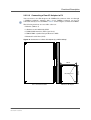
A11 – 6U VMEbus PowerPC Workstation
A11 – 6U VMEbus PowerPC Workstation
The A11 is an industrial PowerPC workstation with scalable performance delivering
up to 1160 MIPS. When equipped with the 603e, the A11 delivers excellent priceperformance for cost-sensitive applications with a need for high computing power.
The board can also be ordered with the 740 PowerPC CPU family for applications
where maximum perfomance is required.
The A11 is a complete state-of-the-art single-board computer needing only one slot
on the VMEbus. It offers fast Ethernet and Ultra2 SCSI controllers, a large amount
of DRAM, Flash and CompactFlash memory. Four serial interfaces are provided two of them default as COM3 and COM4, and the others as COM1 and COM2
directly at the front panel or via a transition module.
The A11 offers computer I/O flexibility by providing two slots for PC•MIP
mezzanine modules, while still providing full front-panel connectivity. Both Type I
and Type II PC•MIP modules can be used to equip the A11 with a full range of
workstation and industrial I/O options. Graphics for VGA, additional Ethernet or
SCSI for server or redundancy purposes, fieldbus interfaces for remote I/O control,
and many others are available, depending on the application.
The A11 CPU board is compatible with Motorola's PowerPC computer boards
(MVME1600 and MVME2600) and offers I/O compatibility with many existing P2
transition modules from Motorola (MVME712M) and other vendors.
MEN Mikro Elektronik GmbH
20A011-00 E4 - 2004-04-20
2
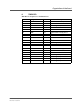
Technical Data
Technical Data
CPU
• Motorola PowerPC
- 603e / 100..300MHz, up to 423 MIPS @ 300MHz
- 740 / 200..500MHz, up to 928 MIPS @ 500MHz
Memory
• Level 1 Cache
- 603e: 16KB instruction/16KB data
- 740: 32KB instruction/32KB data
• Level 2 Cache
- Up to 512KB
• SDRAM soldered 32MB
- 64-bit data bus
- 66MHz
- No parity checking
• SO-DIMM slot up to 64MB
• Flash up to 16MB
- 64-bit data bus
- Two banks
• CompactFlash card interface for Flash ATA via on-board IDE
Local PCI Bus
•
•
•
•
MPC106 Host-to-PCI bridge
PCI Spec. 2.1 compliant
32 bit data bus, 33MHz
One local PCI expansion slot, e.g. for carrier boards with PMC or IP modules
VMEbus
•
•
•
•
•
•
•
•
•
•
•
VMEbus Spec. IEEE-1014-87 compatible
VME64x extension except A64
3-row or 5-row connectors
Tundra Universe II chip
Up to 70MB/s transfer rate
A16, A24, A32 master/slave
D08(EO), D16, D32, D64
BLT, ADOH, RMW, LOCK
7-level interrupter
7-level interrupt handler
System controller
PC-MIP Mezzanine Extension
• Two PC-MIPs Type I/II
• On local PCI bus via DEC21150 PCI-to-PCI bridge
• Compliant with PC-MIP specification
MEN Mikro Elektronik GmbH
20A011-00 E4 - 2004-04-20
3
Technical Data
Interfaces
• COM1/2 with RS232 interface at 9-pin micro D-Sub connector at front panel or
via P2 I/O
• COM3/4 sync./async. UART Z85230 via P2 I/O
• Standard floppy disk controller interface using on-board connector
• Ultra2 SCSI with LVD interface on front panel or 16/8-bit interface at P2 I/O
• Full-duplex 10/100Mbits/s PCI Ethernet controller with 100Base-TX/10Base-T
interface at front panel and 10Base-5 interface via P2 I/O
• Keyboard and mouse with 6-pin PS/2 connector at front panel
• Multimode parallel port (ECP, EPP, PS/2, SPP) via P2 I/O
• IDE interface on-board for AD35 CompactFlash adapter
Miscellaneous
• Real-time clock with 8Kx8 NVRAM
• 6 programmable 16-bit timers Z8536
• Hardware monitor with alarm function for
- On-board temperature control
- Voltage control
• Reset/abort button at front panel
• Four user LEDs at front panel
• Four control LEDs at front panel
• Hex switch for user settings
• Watchdog
Electrical Specifications
• Supply voltage/power consumption: +5V (4.85V..5.25V), 5.5A max.
• MTBF: 66,000h @ 50°C
Mechanical Specifications
• Dimensions: standard double Eurocard, 233.3mm x 160mm
• Weight: 384g
Environmental Specifications
• Temperature range (operation):
- 0..+60°C
- Industrial temperature range on request
- Airflow: min. 10m³/h
• Temperature range (storage): -40..+85°C
• Relative humidity (operation): max. 95% non-condensing
• Relative humidity (storage): max. 95% non-condensing
• Altitude: -300m to + 3,000m
• Shock: 15g/0.33ms, 6g/6ms
• Vibration: 1g/5..2,000Hz
MEN Mikro Elektronik GmbH
20A011-00 E4 - 2004-04-20
4
Technical Data
Safety
• PCB manufactured with a flammability rating of 94V-0 by UL recognized manufacturers
EMC
• Tested according to EN 55022 / 1999-05 (radio disturbance) and EN 55024 /
1999-05 (immunity) with regard to CE conformity
Software Support
•
•
•
•
MENMON
VxWorks
QNX
OS-9
MEN Mikro Elektronik GmbH
20A011-00 E4 - 2004-04-20
5
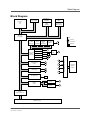
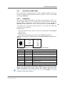
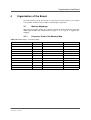
Block Diagram
Block Diagram
L2 Cache
up to 512KB
PowerPC
603e
740
DRAM Bank 1
up to 64MB
SO-DIMM
Flash Bank 1
8MB
DRAM Bank 0
32MB
SDRAM
Flash Bank 0
8MB (optional)
A32/D64 PowerPC Bus
MPC106
Host Bridge
D64 Memory Bus
Legend:
Temperature Counter/
Power
Timer
Manager
CIO Z8536
8Kx8
NVRAM,
RTC,
Watchdog
Sync. UART
COM3/4
R
R
Rear (P2)
F
Front Panel
B
On Board
ISA Bus
Mouse/Keyboard
PCI-to-ISA
Bridge
Super I/O
F
CompactFlash
IDE
Floppy Disk
F
B
COM1/2
F R
Enhanced Parallel
R
Local
PCI
Bus
Ethernet
10/100Base-T
21143
Rear VMEbus P2 Connector
R
D32
F
R
R
R
F
Ultra2 SCSI
SYM53C885
R
R
PCI Expansion
B
PCI Bus
PCI-to-PCI
Bridge
21150
Rear I/O
Adapter
AD39
PC•MIP
Type II
F
PC•MIP
Type II
F
PCI-to-VMEbus
Bridge
Tundra Universe II
VME64 Interface
MEN Mikro Elektronik GmbH
20A011-00 E4 - 2004-04-20
6
Product Safety
Product Safety
!
Lithium Battery
This board contains a lithium battery. There is a danger of explosion if the
battery is incorrectly replaced!
Replace only with the same or equivalent type.
Dispose of used batteries according to the manufacturer's instructions.
!
Fuses
This board contains fuses. If you need to replace a fuse, make sure you adhere to the
following types and ratings:
Component Current Rating
Type
Size
Function
S1
1.5A
Fast
1206
SCSI Termination Power
S2
1.5A
Fast
1206
Keyboard interface
S3
1.5A
Fast
1206
IDE interface
S4
1.5A
Fast
1206
Floppy disk interface
S5
1.5A
Fast
1206
Ethernet P2 interface
For component locations, see Figure 21, Component Plan of A11 Hardware
Revision 03 — Bottom Side, on page 106.
!
Electrostatic Discharge (ESD)
Computer boards and components contain electrostatic sensitive devices.
Electrostatic discharge (ESD) can damage components. To protect the board and
other components against damage from static electricity, you should follow some
precautions whenever you work on your computer.
• Power down and unplug your computer system when working on the inside.
• Hold components by the edges and try not to touch the IC chips, leads, or circuitry.
• Use a grounded wrist strap before handling computer components.
• Place components on a grounded antistatic pad or on the bag that came with the
component whenever the components are separated from the system.
• Store the board only in its original ESD-protected packaging. Retain the original
packaging in case you need to return the board to MEN for repair.
MEN Mikro Elektronik GmbH
20A011-00 E4 - 2004-04-20
7
About this Document
About this Document
This user manual describes the hardware functions of the board, connection of
peripheral devices and integration into a system. It also provides additional
information for special applications and configurations of the board.
The manual does not include detailed information on individual components (data
sheets etc.). A list of literature is given in the appendix.
History
Edition
Description
Technical Content
Date of Issue
E1
First edition
J. Steinert, U. Franke
1999-08-20
E2
Second edition, MENMON
version 2.x
J. Steinert, Klaus Popp
2000-02-14
E3
Third edition, MENMON
version 3.x
J. Steinert, Klaus Popp
2001-03-09
E4
Fourth edition
H. Schubert, U. Franke
2004-04-20
Conventions
!
italics
bold
hyperlink
This sign marks important notes or warnings concerning proper functionality of the
product described in this document. You should read them in any case.
Folder and file names are printed in italics.
Bold type is used for emphasis.
Hyperlinks are printed in blue color.
The globe will show you where hyperlinks lead directly to the Internet, so you can
look for the latest information online.
0xFF
Hexadecimal numbers are preceded by "0x", which is the usual C-language
convention, and are printed in a monospace type, e.g. 0x00FFFF.
IRQ#
/IRQ
Signal names followed by "#" or preceded by a slash ("/") indicate that this signal is
either active low or that it becomes active at a falling edge.
in/out
Signal directions in signal mnemonics tables generally refer to the corresponding
board or component, "in" meaning "to the board or component", "out" meaning
"coming from it".
Vertical lines on the outer margin signal technical changes to the previous edition of
the document.
MEN Mikro Elektronik GmbH
20A011-00 E4 - 2004-04-20
8
About this Document
Copyright Information
MEN reserves the right to make changes without further notice to any products herein. MEN makes no
warranty, representation or guarantee regarding the suitability of its products for any particular
purpose, nor does MEN assume any liability arising out of the application or use of any product or
circuit, and specifically disclaims any and all liability, including without limitation consequential or
incidental damages.
"Typical" parameters can and do vary in different applications. All operating parameters, including
"Typicals" must be validated for each customer application by customer's technical experts.
MEN does not convey any license under its patent rights nor the rights of others.
MEN products are not designed, intended, or authorized for use as components in systems intended for
surgical implant into the body, or other applications intended to support or sustain life, or for any other
application in which the failure of the MEN product could create a situation where personal injury or
death may occur. Should Buyer purchase or use MEN products for any such unintended or
unauthorized application, Buyer shall indemnify and hold MEN and its officers, employees,
subsidiaries, affiliates, and distributors harmless against all claims, costs, damages, and expenses, and
reasonable attorney fees arising out of, directly or indirectly, any claim of personal injury or death
associated with such unintended or unauthorized use, even if such claim alleges that MEN was
negligent regarding the design or manufacture of the part.
All brand or product names are trademarks or registered trademarks of their respective holders.
Information in this document has been carefully checked and is believed to be accurate as of the date of
publication; however, no responsibility is assumed for inaccuracies. MEN will not be liable for any
consequential or incidental damages arising from reliance on the accuracy of this document. The
information contained herein is subject to change without notice.
Copyright © 2004 MEN Mikro Elektronik GmbH. All rights reserved.
Please recycle
Germany
MEN Mikro Elektronik GmbH
Neuwieder Straße 5-7
90411 Nuremberg
Phone +49-911-99 33 5-0
Fax +49-911-99 33 5-901
E-mail [email protected]
www.men.de
France
MEN Mikro Elektronik SA
18, rue René Cassin
ZA de la Châtelaine
74240 Gaillard
Phone +33 (0) 450-955-312
Fax +33 (0) 450-955-211
E-mail [email protected]
www.men-france.fr
MEN Mikro Elektronik GmbH
20A011-00 E4 - 2004-04-20
UK
MEN Micro Ltd
Whitehall, 75 School Lane
Hartford, Northwich
Cheshire UK, CW8 1PF
Phone +44 (0) 1477-549-185
Fax +44 (0) 1477-549-178
E-mail [email protected]
www.menmicro.co.uk
USA
MEN Micro, Inc.
3740 North Josey Lane, Suite 203
Carrollton, TX 75007
Phone 972-939-2675
Fax 972-939-0055
E-mail [email protected]
www.menmicro.com
9
Contents
Contents
1 Getting Started . . . . . . . . . . . . . . . . . . . . . . . . . . . . . . . . . . . . . . . . . . . . . . . .
1.1 Map of the Board. . . . . . . . . . . . . . . . . . . . . . . . . . . . . . . . . . . . . . . . .
1.2 Configuring the Hardware . . . . . . . . . . . . . . . . . . . . . . . . . . . . . . . . . .
1.3 Integrating the Board into a System . . . . . . . . . . . . . . . . . . . . . . . . . .
1.4 Installing Operating System Software. . . . . . . . . . . . . . . . . . . . . . . . .
16
16
17
18
19
2 Functional Description . . . . . . . . . . . . . . . . . . . . . . . . . . . . . . . . . . . . . . . . . .
2.1 Power Supply. . . . . . . . . . . . . . . . . . . . . . . . . . . . . . . . . . . . . . . . . . . .
2.2 Clock Supply . . . . . . . . . . . . . . . . . . . . . . . . . . . . . . . . . . . . . . . . . . . .
2.3 PowerPC CPU . . . . . . . . . . . . . . . . . . . . . . . . . . . . . . . . . . . . . . . . . . .
2.3.1
General . . . . . . . . . . . . . . . . . . . . . . . . . . . . . . . . . . . . . . . . .
2.3.2
Heat Sink. . . . . . . . . . . . . . . . . . . . . . . . . . . . . . . . . . . . . . . .
2.4 Bus Structure . . . . . . . . . . . . . . . . . . . . . . . . . . . . . . . . . . . . . . . . . . . .
2.4.1
Host-to-PCI Bridge . . . . . . . . . . . . . . . . . . . . . . . . . . . . . . . .
2.4.2
Local PCI Bus . . . . . . . . . . . . . . . . . . . . . . . . . . . . . . . . . . . .
2.4.3
PCI-to-ISA Bridge . . . . . . . . . . . . . . . . . . . . . . . . . . . . . . . .
2.4.4
PCI-to-PCI Bridge. . . . . . . . . . . . . . . . . . . . . . . . . . . . . . . . .
2.4.5
PCI-to-VMEbus Bridge . . . . . . . . . . . . . . . . . . . . . . . . . . . .
2.5 Memory . . . . . . . . . . . . . . . . . . . . . . . . . . . . . . . . . . . . . . . . . . . . . . . .
2.5.1
Level 2 Cache . . . . . . . . . . . . . . . . . . . . . . . . . . . . . . . . . . . .
2.5.2
SDRAM . . . . . . . . . . . . . . . . . . . . . . . . . . . . . . . . . . . . . . . .
2.5.3
Flash . . . . . . . . . . . . . . . . . . . . . . . . . . . . . . . . . . . . . . . . . . .
2.5.4
EEPROM. . . . . . . . . . . . . . . . . . . . . . . . . . . . . . . . . . . . . . . .
2.6 Ethernet Interface . . . . . . . . . . . . . . . . . . . . . . . . . . . . . . . . . . . . . . . .
2.6.1
Connection . . . . . . . . . . . . . . . . . . . . . . . . . . . . . . . . . . . . . .
2.6.2
General . . . . . . . . . . . . . . . . . . . . . . . . . . . . . . . . . . . . . . . . .
2.6.3
10Base-5 . . . . . . . . . . . . . . . . . . . . . . . . . . . . . . . . . . . . . . . .
2.6.4
10Base-T . . . . . . . . . . . . . . . . . . . . . . . . . . . . . . . . . . . . . . . .
2.6.5
100Base-T . . . . . . . . . . . . . . . . . . . . . . . . . . . . . . . . . . . . . . .
2.7 SCSI Interface . . . . . . . . . . . . . . . . . . . . . . . . . . . . . . . . . . . . . . . . . . .
2.7.1
Connection . . . . . . . . . . . . . . . . . . . . . . . . . . . . . . . . . . . . . .
2.7.2
General . . . . . . . . . . . . . . . . . . . . . . . . . . . . . . . . . . . . . . . . .
2.7.3
SCSI Termination on A11. . . . . . . . . . . . . . . . . . . . . . . . . . .
2.8 PCI Expansion . . . . . . . . . . . . . . . . . . . . . . . . . . . . . . . . . . . . . . . . . . .
2.9 PC•MIP Slots. . . . . . . . . . . . . . . . . . . . . . . . . . . . . . . . . . . . . . . . . . . .
2.9.1
Installing PC•MIPs . . . . . . . . . . . . . . . . . . . . . . . . . . . . . . . .
2.9.2
PC•MIP Connectors . . . . . . . . . . . . . . . . . . . . . . . . . . . . . . .
2.10 CompactFlash . . . . . . . . . . . . . . . . . . . . . . . . . . . . . . . . . . . . . . . . . . .
2.10.1 Installing CompactFlash . . . . . . . . . . . . . . . . . . . . . . . . . . . .
2.10.2 Supported CompactFlash Cards . . . . . . . . . . . . . . . . . . . . . .
2.11 Keyboard/Mouse . . . . . . . . . . . . . . . . . . . . . . . . . . . . . . . . . . . . . . . . .
2.12 Serial Ports COM1/COM2 . . . . . . . . . . . . . . . . . . . . . . . . . . . . . . . . .
2.12.1 Connection . . . . . . . . . . . . . . . . . . . . . . . . . . . . . . . . . . . . . .
20
20
20
21
21
21
22
22
22
22
22
22
23
23
23
24
24
25
25
26
26
26
27
28
28
30
32
33
35
35
36
37
37
37
38
39
39
MEN Mikro Elektronik GmbH
20A011-00 E4 - 2004-04-20
10
Contents
2.13
2.14
2.15
2.16
2.17
2.18
2.19
Asynchronous/Synchronous Serial Ports COM3/COM4 . . . . . . . . . .
Enhanced Parallel Port. . . . . . . . . . . . . . . . . . . . . . . . . . . . . . . . . . . . .
Floppy Disk Controller . . . . . . . . . . . . . . . . . . . . . . . . . . . . . . . . . . . .
Hardware Monitor . . . . . . . . . . . . . . . . . . . . . . . . . . . . . . . . . . . . . . . .
Timekeeper, NVRAM and Watchdog . . . . . . . . . . . . . . . . . . . . . . . . .
Counter/Timer CIO Z8536 . . . . . . . . . . . . . . . . . . . . . . . . . . . . . . . . .
Reset/Abort Buttons and User/Status LEDs . . . . . . . . . . . . . . . . . . . .
2.19.1 Reset/Abort Buttons . . . . . . . . . . . . . . . . . . . . . . . . . . . . . . .
2.19.2 User/Status LEDs . . . . . . . . . . . . . . . . . . . . . . . . . . . . . . . . .
2.20 User-Defined Hex Switch . . . . . . . . . . . . . . . . . . . . . . . . . . . . . . . . . .
2.21 VMEbus Interface . . . . . . . . . . . . . . . . . . . . . . . . . . . . . . . . . . . . . . . .
2.21.1 Implementation on the Board . . . . . . . . . . . . . . . . . . . . . . . .
2.21.2 Connection . . . . . . . . . . . . . . . . . . . . . . . . . . . . . . . . . . . . . .
2.22 IEEE 1149.1 (JTAG)/COP Test Interface . . . . . . . . . . . . . . . . . . . . . .
2.22.1 Configuring the IEEE 1149.1 Test Interface . . . . . . . . . . . . .
2.22.2 Configuring the COP Test Interface . . . . . . . . . . . . . . . . . . .
40
41
42
44
44
44
45
45
45
46
47
47
49
55
56
56
3 MENMON . . . . . . . . . . . . . . . . . . . . . . . . . . . . . . . . . . . . . . . . . . . . . . . . . . . .
3.1 General . . . . . . . . . . . . . . . . . . . . . . . . . . . . . . . . . . . . . . . . . . . . . . . .
3.2 Console . . . . . . . . . . . . . . . . . . . . . . . . . . . . . . . . . . . . . . . . . . . . . . . .
3.3 A11 MENMON Memory Map . . . . . . . . . . . . . . . . . . . . . . . . . . . . . .
3.4 MENMON Start-up . . . . . . . . . . . . . . . . . . . . . . . . . . . . . . . . . . . . . . .
3.4.1
User LEDs. . . . . . . . . . . . . . . . . . . . . . . . . . . . . . . . . . . . . . .
3.4.2
Boot Sequence. . . . . . . . . . . . . . . . . . . . . . . . . . . . . . . . . . . .
3.4.3
Configuring the MENMON Start-up Procedure . . . . . . . . . .
3.4.4
Self Tests . . . . . . . . . . . . . . . . . . . . . . . . . . . . . . . . . . . . . . . .
3.5 MENMON Boot Methods for Client Programs . . . . . . . . . . . . . . . . .
3.5.1
MENMON BIOS Devices. . . . . . . . . . . . . . . . . . . . . . . . . . .
3.5.2
Disk Boot . . . . . . . . . . . . . . . . . . . . . . . . . . . . . . . . . . . . . . .
3.5.3
Network Boot . . . . . . . . . . . . . . . . . . . . . . . . . . . . . . . . . . . .
3.5.4
MENMON Tape Boot . . . . . . . . . . . . . . . . . . . . . . . . . . . . . .
3.6 Updating Flash Devices. . . . . . . . . . . . . . . . . . . . . . . . . . . . . . . . . . . .
3.6.1
Download via Serial Interface. . . . . . . . . . . . . . . . . . . . . . . .
3.6.2
Performing the Download . . . . . . . . . . . . . . . . . . . . . . . . . . .
3.6.3
Update from Disk or Network. . . . . . . . . . . . . . . . . . . . . . . .
3.7 MENMON User Interface . . . . . . . . . . . . . . . . . . . . . . . . . . . . . . . . . .
3.7.1
Command Line Editing . . . . . . . . . . . . . . . . . . . . . . . . . . . . .
3.7.2
Numerical Arguments . . . . . . . . . . . . . . . . . . . . . . . . . . . . . .
3.7.3
MENMON Command Overview . . . . . . . . . . . . . . . . . . . . .
3.8 Board Setup . . . . . . . . . . . . . . . . . . . . . . . . . . . . . . . . . . . . . . . . . . . . .
3.8.1
ALI 1543 . . . . . . . . . . . . . . . . . . . . . . . . . . . . . . . . . . . . . . . .
3.8.2
PCI Auto-Configuration . . . . . . . . . . . . . . . . . . . . . . . . . . . .
3.8.3
VMEbus . . . . . . . . . . . . . . . . . . . . . . . . . . . . . . . . . . . . . . . .
3.8.4
SCSI . . . . . . . . . . . . . . . . . . . . . . . . . . . . . . . . . . . . . . . . . . .
3.8.5
SDRAM DIMM Configuration. . . . . . . . . . . . . . . . . . . . . . .
3.8.6
Hex Switch . . . . . . . . . . . . . . . . . . . . . . . . . . . . . . . . . . . . . .
57
57
57
58
59
59
59
59
60
62
62
64
70
71
72
72
73
74
75
75
75
76
78
78
78
80
81
81
81
MEN Mikro Elektronik GmbH
20A011-00 E4 - 2004-04-20
11
Contents
3.9 MENMON System Calls . . . . . . . . . . . . . . . . . . . . . . . . . . . . . . . . . . .
3.9.1
Invoking System Calls. . . . . . . . . . . . . . . . . . . . . . . . . . . . . .
3.9.2
System Calls . . . . . . . . . . . . . . . . . . . . . . . . . . . . . . . . . . . . .
3.10 VxWorks Bootline . . . . . . . . . . . . . . . . . . . . . . . . . . . . . . . . . . . . . . . .
3.10.1 Additional MENMON Parameters . . . . . . . . . . . . . . . . . . . .
82
82
83
88
89
4 Organization of the Board . . . . . . . . . . . . . . . . . . . . . . . . . . . . . . . . . . . . . . .
4.1 Memory Mappings . . . . . . . . . . . . . . . . . . . . . . . . . . . . . . . . . . . . . . .
4.1.1
Processor View of the Memory Map. . . . . . . . . . . . . . . . . . .
4.1.2
PCI Configuration Space Map (Primary Bus) . . . . . . . . . . .
4.1.3
PCI Configuration Space Map (Secondary Bus) . . . . . . . . .
4.1.4
PCI/ISA I/O Space Memory Map . . . . . . . . . . . . . . . . . . . . .
4.1.5
VMEbus Memory Map . . . . . . . . . . . . . . . . . . . . . . . . . . . . .
4.2 Interrupt Handling . . . . . . . . . . . . . . . . . . . . . . . . . . . . . . . . . . . . . . . .
4.2.1
Nonmaskable Interrupts . . . . . . . . . . . . . . . . . . . . . . . . . . . .
4.2.2
Maskable Interrupts. . . . . . . . . . . . . . . . . . . . . . . . . . . . . . . .
4.3 Implementation of SYM53C895 SCSI Controller . . . . . . . . . . . . . . .
4.4 Implementation of M1543 PCI-to-ISA Bridge . . . . . . . . . . . . . . . . . .
4.5 Z8536 CIO. . . . . . . . . . . . . . . . . . . . . . . . . . . . . . . . . . . . . . . . . . . . . .
90
90
90
91
91
92
93
94
95
95
96
97
99
5 Appendix . . . . . . . . . . . . . . . . . . . . . . . . . . . . . . . . . . . . . . . . . . . . . . . . . . . .
5.1 Literature and WWW Resources. . . . . . . . . . . . . . . . . . . . . . . . . . . .
5.1.1
Bridges . . . . . . . . . . . . . . . . . . . . . . . . . . . . . . . . . . . . . . . .
5.1.2
VMEbus . . . . . . . . . . . . . . . . . . . . . . . . . . . . . . . . . . . . . . .
5.1.3
PCI . . . . . . . . . . . . . . . . . . . . . . . . . . . . . . . . . . . . . . . . . . .
5.1.4
Ethernet . . . . . . . . . . . . . . . . . . . . . . . . . . . . . . . . . . . . . . . .
5.1.5
SCSI . . . . . . . . . . . . . . . . . . . . . . . . . . . . . . . . . . . . . . . . . .
5.1.6
Parallel Port. . . . . . . . . . . . . . . . . . . . . . . . . . . . . . . . . . . . .
5.1.7
PC•MIP . . . . . . . . . . . . . . . . . . . . . . . . . . . . . . . . . . . . . . . .
5.1.8
Miscellaneous . . . . . . . . . . . . . . . . . . . . . . . . . . . . . . . . . . .
5.2 Board Revisions. . . . . . . . . . . . . . . . . . . . . . . . . . . . . . . . . . . . . . . . .
5.3 Component Plans. . . . . . . . . . . . . . . . . . . . . . . . . . . . . . . . . . . . . . . .
MEN Mikro Elektronik GmbH
20A011-00 E4 - 2004-04-20
100
100
100
100
100
101
101
101
102
102
102
105
12
Figures
Figure 1.
Figure 2.
Figure 3.
Figure 4.
Figure 5.
Figure 6.
Figure 7.
Figure 8.
Map of the Board - Front Panel and Top View . . . . . . . . . . . . . . . . . . 16
SO-DIMM DRAM Installation . . . . . . . . . . . . . . . . . . . . . . . . . . . . . . 23
Position of Flash on Bottom Side of A11. . . . . . . . . . . . . . . . . . . . . . . 24
SCSI Termination on A11 . . . . . . . . . . . . . . . . . . . . . . . . . . . . . . . . . . 32
Installation of a PC•MIP. . . . . . . . . . . . . . . . . . . . . . . . . . . . . . . . . . . . 35
CompactFlash Card . . . . . . . . . . . . . . . . . . . . . . . . . . . . . . . . . . . . . . . 37
COM4 Clock Signals — Principle . . . . . . . . . . . . . . . . . . . . . . . . . . . . 40
Jumpers for Clock Selection for COM4 (Default Setting: all jumpers
removed) . . . . . . . . . . . . . . . . . . . . . . . . . . . . . . . . . . . . . . . . . . . . . . . . 41
Figure 9. Reset/Abort Buttons and User LEDs . . . . . . . . . . . . . . . . . . . . . . . . . . 45
Figure 10. Position of Hex Switch . . . . . . . . . . . . . . . . . . . . . . . . . . . . . . . . . . . . . 46
Figure 11. VMEbus Interrupts . . . . . . . . . . . . . . . . . . . . . . . . . . . . . . . . . . . . . . . . 48
Figure 12. Connection of a Rear I/O Adapter (e.g. MEN’s AD39) . . . . . . . . . . . . 54
Figure 13. Connector and Jumper for IEEE 1149.1 Test Interface . . . . . . . . . . . . 56
Figure 14. Resistors for COP Test Interface . . . . . . . . . . . . . . . . . . . . . . . . . . . . . 56
Figure 15. MENMON — Address Mapping . . . . . . . . . . . . . . . . . . . . . . . . . . . . . 58
Figure 16. MENMON — Power On Self Test Output with Self Test Message Mode
EXTENDED . . . . . . . . . . . . . . . . . . . . . . . . . . . . . . . . . . . . . . . . . . . . . 60
Figure 17. MENMON — Layout of the 0x41-Type Partition (PReP) . . . . . . . . . 64
Figure 18. MENMON — Single Boot-Image CD-ROM Configuration . . . . . . . . 65
Figure 19. A11 Interrupt Structure. . . . . . . . . . . . . . . . . . . . . . . . . . . . . . . . . . . . . 94
Figure 20. Component Plan of A11 Hardware Revision 03 — Top Side . . . . . . 105
Figure 21. Component Plan of A11 Hardware Revision 03 — Bottom Side . . . 106
MEN Mikro Elektronik GmbH
20A011-00 E4 - 2004-04-20
13
Tables
Table 1.
Table 2.
Table 3.
Table 4.
Table 5.
Table 6.
Table 7.
Table 8.
Table 9.
Table 10.
Table 11.
Table 12.
Table 13.
Table 14.
Table 15.
Table 16.
Table 17.
Table 18.
Table 19.
Table 20.
Table 21.
Table 22.
Table 23.
Table 24.
Table 25.
Table 26.
Table 27.
Table 28.
Table 29.
Table 30.
Table 31.
Table 32.
Table 33.
Table 34.
Table 35.
Table 36.
Table 37.
MEN Mikro Elektronik GmbH
20A011-00 E4 - 2004-04-20
Terminal Lines of the 9-pin micro D-Sub RS232 Plug Connector
(COM1) . . . . . . . . . . . . . . . . . . . . . . . . . . . . . . . . . . . . . . . . . . . . . . . . 18
PowerPC Compare Chart . . . . . . . . . . . . . . . . . . . . . . . . . . . . . . . . . . . 21
Pin Assignment of the 8-pin RJ45 Ethernet 10Base-T/100Base-T
Connector . . . . . . . . . . . . . . . . . . . . . . . . . . . . . . . . . . . . . . . . . . . . . . . 25
Signal Mnemonics of the Ethernet 10Base-T/100Base-T Connector . 25
Signal Mnemonics for SCSI Interface . . . . . . . . . . . . . . . . . . . . . . . . . 28
Pin Assignment of the 68-pin VHDCI SCSI Connector . . . . . . . . . . . 29
Overview of SCSI Types, Maximum Bus Widths, Throughput and Line
Lengths . . . . . . . . . . . . . . . . . . . . . . . . . . . . . . . . . . . . . . . . . . . . . . . . . 31
SCSI Termination on A11 . . . . . . . . . . . . . . . . . . . . . . . . . . . . . . . . . . 32
Pin Assignment of the 114-pin PCI Expansion Connector . . . . . . . . . 34
Pin Assignment of the 6-Pin Mini DIN Keyboard/Mouse Connector . 38
Signal Mnemonics for Keyboard/Mouse Interface . . . . . . . . . . . . . . . 38
Pin Assignment of the 9-pin micro D-Sub COM1/COM2 Plug Connectors
(RS232). . . . . . . . . . . . . . . . . . . . . . . . . . . . . . . . . . . . . . . . . . . . . . . . . 39
Signal Mnemonics for RS232 Serial Ports COM1/COM2. . . . . . . . . . 39
Configuring Clock Signals for COM4 . . . . . . . . . . . . . . . . . . . . . . . . . 40
Pin Assignment of 26-pin ZIF Floppy Disk Drive Connector . . . . . . . 42
Signal Mnemonics for Floppy Disk Drive Connector . . . . . . . . . . . . . 43
Hardware Monitor Channels . . . . . . . . . . . . . . . . . . . . . . . . . . . . . . . . 44
User/Status LED Functions . . . . . . . . . . . . . . . . . . . . . . . . . . . . . . . . . 45
Pin Assignment of the 5/3-Row, 96/160-Pin VMEbus Connector P1 . 50
Pin Assignment of the 5/3-Row, 96/160-Pin VMEbus Connector P2 . 51
Signal Mnemonics of VMEbus Rear I/O Connector P2. . . . . . . . . . . . 52
Pin Assignment of the 16-pin IEEE 1149.1 Test Connector . . . . . . . . 55
MENMON — Assignment for A11 Controller Devices . . . . . . . . . . . 63
MENMON — Download Destination Devices . . . . . . . . . . . . . . . . . . 72
MENMON — Flash Sectors for 8MB . . . . . . . . . . . . . . . . . . . . . . . . . 73
MENMON — Flash Sectors for 16MB . . . . . . . . . . . . . . . . . . . . . . . . 73
MENMON — Command Overview. . . . . . . . . . . . . . . . . . . . . . . . . . . 76
MENMON — Address Map for A11 as a VMEbus Master . . . . . . . . 80
MENMON — Hex-Switch Settings . . . . . . . . . . . . . . . . . . . . . . . . . . . 81
MENMON — System Calls — BRD_ID Fields . . . . . . . . . . . . . . . . . 83
MENMON — System Calls — RTC_RD Buffer Data . . . . . . . . . . . . 85
MENMON — System Calls — DSK_RD Fields. . . . . . . . . . . . . . . . . 86
MENMON — VxWorks Bootline — List of Parameters and their
Usage . . . . . . . . . . . . . . . . . . . . . . . . . . . . . . . . . . . . . . . . . . . . . . . . . . 88
MENMON - Common Parameters Passed by All MENMONs . . . . . . 89
Address Map — Processor View . . . . . . . . . . . . . . . . . . . . . . . . . . . . . 90
PCI Configuration Space Map (Primary Bus) . . . . . . . . . . . . . . . . . . . 91
PCI Configuration Space Map (Secondary Bus) . . . . . . . . . . . . . . . . . 91
14
Table 38.
Table 39.
Table 40.
Table 41.
Table 42.
Table 43.
Table 44.
Table 45.
Table 46.
Table 47.
Table 48.
Table 49.
MEN Mikro Elektronik GmbH
20A011-00 E4 - 2004-04-20
PCI/ISA I/O Space Memory Map . . . . . . . . . . . . . . . . . . . . . . . . . . . . 92
Possible VMEbus Memory Map . . . . . . . . . . . . . . . . . . . . . . . . . . . . . 93
ISA Interrupt Assignments . . . . . . . . . . . . . . . . . . . . . . . . . . . . . . . . . . 95
Steerable Interrupt Assignments. . . . . . . . . . . . . . . . . . . . . . . . . . . . . . 95
PCI Interrupt Assignments . . . . . . . . . . . . . . . . . . . . . . . . . . . . . . . . . . 95
General-Purpose Pins of SYM53C895 SCSI Controller . . . . . . . . . . . 96
M1543 General Purpose Input (GPI) Pin Assignments . . . . . . . . . . . . 97
M1543 General Purpose Input/Output (GPIO) Pin Assignments . . . . 97
M1543 General Purpose Output Pin Assignments . . . . . . . . . . . . . . . . 98
M1543 GPI Assignment for Hex Switch . . . . . . . . . . . . . . . . . . . . . . . 98
Pin Assignment of the Z8536 Ports . . . . . . . . . . . . . . . . . . . . . . . . . . . 99
Table of Hardware Revisions . . . . . . . . . . . . . . . . . . . . . . . . . . . . . . . 102
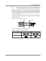
15
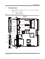
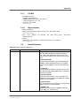
Getting Started
1
Getting Started
This chapter will give an overview of the A11 and some hints for first installation in
a VMEbus system as a "check list".
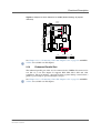
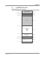
1.1
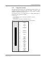
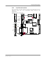
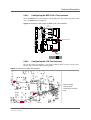
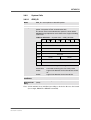
Map of the Board
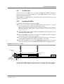
Figure 1. Map of the Board - Front Panel and Top View
Injectors/Ejectors
with Threaded
Standoffs and
Captive Screws
P2
P3
PC•MIP slot 1
SO-DIMM
DRAM
Socket
P1
VMEbus P1
Finished Bezel
of PC•MIP I/O
Connector
P2
P3
PC•MIP slot 2
PC•MIP
Keeper Screw
(solder side)
P1
Ethernet
10Base-T/100Base-T
Keyboard/Mouse
PCI
Bridge
PowerPC
Processor
Core
Tundra
Universe II
VMEbus
Controller
User LEDs
COM2
Abort Button
Reset Button
SCSI
Interface
CompactFlash
Card Slot
IEEE
1149.1/
COP Test
Interface
VMEbus P2
COM1
PCI Extension Slot
PC•MIP Bezel
Keepers
Southbridge
Floppy Disk
Drive Interface
P4 P5 P7 P6
User-defined Hex Switch
MEN Mikro Elektronik GmbH
20A011-00 E4 - 2004-04-20
Configuration Jumpers
16
Getting Started
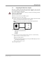
1.2
Configuring the Hardware
You should check your hardware requirements before installing the board in a
system, since most modifications are difficult or even impossible to do when the
board is mounted in an enclosure.
The following check list will give an overview on what you might want to configure.
DRAM SO-DIMM modules
The A11 is shipped with 32MB DRAM on board. You should check on your
main memory needs and install a suitable SO-DIMM module if necessary.
Refer to Chapter 2.5.2 SDRAM on page 23 for a detailed installation
description and hints on supported SO-DIMM modules.
CompactFlash
Refer to Chapter 2.10 CompactFlash on page 37 for a detailed
installation description and hints on supported CompactFlash cards.
PC•MIPs
Refer to Chapter 2.9.1 Installing PC•MIPs on page 35 for a detailed
installation description. Also, observe the installation recommendations
given in the M-Module’s user manual.
Rear I/O adapter
Refer to Chapter 2.21.2.3 Connecting a Rear I/O Adapter to P2 on page
54 for hints on connection of a rear I/O adapter.
PCI Expansion
Refer to Chapter 2.8 PCI Expansion on page 33 for more information on
possible PCI expansion.
MEN Mikro Elektronik GmbH
20A011-00 E4 - 2004-04-20
17
Getting Started
1.3
Integrating the Board into a System
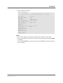
The A11 is a complex board and setting it up requires experience. You can use the
following check list when installing the CPU board in a VMEbus system for the first
time and with minimum configuration.
!
The board is completely trimmed on delivery. Perform the following procedure
without a PC•MIP installed!
Power-down the system.
Remove all boards from the VMEbus system.
Install the A11 in slot 1 of the system.
Connect a terminal to the standard RS232 interface COM1 (9-pin micro D-Sub
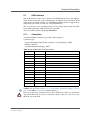
connector) by wiring the following lines to the connector:
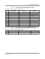
Table 1. Terminal Lines of the 9-pin micro D-Sub RS232 Plug Connector
(COM1)
6
9
1
5
6
-
1
-
7
-
2
RXD
8
-
3
TXD
9
-
4
-
5
GND
Set your terminal to the following protocol:
-
9600 baud data transmission rate
8 data bits
1 stop bit
No parity
Note: If you need to restore these default settings on the A11, do the following:
Press the Reset and Abort buttons at once.
Release the Reset button.
Hold the Abort button until the green front-panel LEDs light up in succession, then release the button.
Press the Reset button again.
Power-up the system.
MEN Mikro Elektronik GmbH
20A011-00 E4 - 2004-04-20
18
Getting Started
The terminal displays the following message:
___________________ Secondary MenMon for the A11 Version 3.0 ________________
|
|
|
(c) 1998 - 2000 MEN mikro elektronik GmbH Nuernberg
|
|
Parts of this code are based on Motorola’s Dink32
|
|
Created Feb 11 2000
13:42:19
|
|_____________________________________________________________________________|
|
HW Revision: 01.01.00
|
CPU: MPC740
|
| Serial Number: 0
|
CPU Clock: 299 MHz
|
| Board Version: 00
|
Onboard RAM: 32 MB
|
|
|
DIMM Module:
0 MB
|
\___________________________________________________________________________/
Init VME Controller.. (Slot 1 function enabled)
press ’ESC’ to setup/MENMON
Selftest running ...
CHECKSUM
==> OK
*** Can't jump to bootstrapper. BS address in EEPROM invalid!
MenMon>
Now you can use the MENMON debugger (see detailed description in Chapter
3 MENMON on page 57).
Observe the installation instructions for the respective software.
1.4
Installing Operating System Software
The A11 supports VxWorks, OS-9, LynxOS and QNX.
You can find any software available on MEN’s website.
!
By standard, no operating system is installed on the board. Please refer to MEN’s
operating system installation documentation on how to install the software!
MEN Mikro Elektronik GmbH
20A011-00 E4 - 2004-04-20
19
Functional Description
2
Functional Description
The following describes the individual functions of the A11 and their configuration
on the board. There is no detailed description of the individual controller chips and
the CPUs. They can be obtained from the data sheets or data books of the
semiconductor manufacturer concerned (Chapter 5.1 Literature and WWW
Resources on page 100).
2.1
Power Supply
The A11 is supplied with +5V via the VMEbus. However, PC•MIPs, PCI expansion
cards or rear I/O adapters may need +12V.
Two power supplies generate different supply voltages on the board: One is used for
the PowerPC core voltage, which is factory-set for the corresponding processor. The
other converter is fixed to 3.3V. It supplies the PC•MIP PCI bus and the host
memory bus devices.
2.2
Clock Supply
The clock supply generates all clocks for the on-board devices (PowerPC, SDRAM,
L2 Cache, host bridge, PCI bus devices). The clock frequency is factory-set for the
corresponding processor.
The local PCI clock is limited to 33MHz because of the Tundra Universe II
VMEbus chip.
MEN Mikro Elektronik GmbH
20A011-00 E4 - 2004-04-20
20
Functional Description
2.3
PowerPC CPU
The A11 supports the principle of scalable CPU performance. Depending on the
application, the user can choose between 188 MIPS and 629 MIPS of computing
performance.
The board is prepared for different PowerPC™ CPUs. All CPUs are pin- and buscompatible. The CPU is not removable.
2.3.1
General
The PowerPC architecture, developed jointly by Motorola, IBM, and Apple
Computer, is based on the POWER architecture implemented by the RS/6000™
family of computers. The PowerPC architecture takes advantage of recent
technological advances in such areas as process technology, compiler design, and
RISC microprocessor design to provide software compatibility across a diverse
family of implementations, primarily single-chip microprocessors, intended for a
wide range of systems.
To provide a single architecture for such a broad assortment of processor
environments, the PowerPC architecture is both flexible and scalable.
Table 2. PowerPC Compare Chart
1
PowerPC
Core
Voltage
Core
Frequencies
603e1
2.5V
166..300 MHz
1
2
1
16/16 KB
6.0 W
423 MIPS
7401
2.6V
200/233/266 MHz
1
2
2
32/32 KB
7/7.9 W
488 MIPS
740
1.9V
300 MHz
1
2
2
32/32 KB
4.8 W
550 MIPS
740
2.0V
500 MHz
1
2
2
32/32 KB
8W
928 MIPS
FPU
MMU
INT
Instruction/
Data Cache
Max. Power
Max.
Perfomance
Version for extended temperature range -40°C..+85°C available
Refer to MEN’s website for supported PowerPC CPU types.
!
2.3.2
Heat Sink
A heat sink is provided to meet thermal requirements.
!
Note: MEN gives no warranty on functionality and reliability of the A11 if you use
any other processor or heat sink than that supplied by MEN. Please contact
either MEN directly or your local MEN sales office!
MEN Mikro Elektronik GmbH
20A011-00 E4 - 2004-04-20
21
Functional Description
2.4
Bus Structure
2.4.1
Host-to-PCI Bridge
The MPC106 is used as host bridge for the PowerPC processor. All transactions of
the PowerPC to memory or to the PCI bus are controlled by the host bridge.
The A11 supports concurrent transfers on PowerPC and PCI buses.
The PCI interface is PCI bus Rev. 2.1 compliant and supports all bus commands and
transactions. Master and target operations are possible. Big- or little-endian
operation is selectable.
2.4.2
Local PCI Bus
The local PCI bus is controlled by the MPC106 host-to-PCI bridge. It runs at
33MHz. The I/O voltage is fixed to 5V. The data width is 32 bits.
Major functional elements of the A11, such as Ethernet, SCSI, PCI expansion and
PC•MIP extension, are connected on the local PCI bus.
2.4.3
PCI-to-ISA Bridge
The M1543 is the "southbridge" between PCI and ISA bus, providing full PCI and
ISA compatible functions. The M1543 provides integrated Super I/O (floppy disk
controller, 2 serial ports/1 parallel port), system peripherals (ISP) (2 82C59 and
serial interrupt, 1 82C54), advanced features (type F and distributed DMA) in the
DMA controller (2 82C37), PS2 keyboard/mouse controller, 2-channel dedicated
IDE master controller with Ultra-33 specification and System Management Bus
(SMB).
M1543 also provides a PCI-to-ISA IRQ routing table, and level-to-edge trigger
transfer. The chip provides 2 extra IRQ lines and 1 programmable chip. The
interrupt lines can be routed to any of the available ISA interrupts.
2.4.4
PCI-to-PCI Bridge
The A11 has a secondary PCI bus for PC•MIP mezzanines. It is controlled by a
21150 device and has a signaling voltage of 3.3V.
2.4.5
PCI-to-VMEbus Bridge
The Tundra Universe II chip is the bridge from the local board functions to the
VMEbus. The device decouples the transfers between the PCI bus and VMEbus
with the help of transmit and receive FIFOs for both sides.
MEN Mikro Elektronik GmbH
20A011-00 E4 - 2004-04-20
22
Functional Description
2.5
Memory
2.5.1
Level 2 Cache
For high performance the board has 512KB secondary level cache. The cache is
controlled by the MPC106 host bridge.
2.5.2
SDRAM
Two SDRAM banks are implemented on A11. Bank 0 with 32MB is permanently
mounted.
Bank 1 is connected to a 144-pin SO-DIMM connector for easy extension. The
MPC106 can handle SDRAM devices with up to 64Mbit.
2.5.2.1
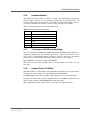
Installing SO-DIMM DRAM
The A11 is normally shipped without any DRAM SO-DIMM module installed. To
install a SO-DIMM module, please stick to the following procedure.
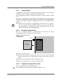
Figure 2. SO-DIMM DRAM Installation
Plastic
Clip
Contact
Groove
Safety
Notch
SO-DIMM Memory Module
SO-DIMM Socket
Safety
Tab
Plastic
Clip
The DRAM module will only fit as shown above because of a safety tab on the SODIMM socket which requires a notch in the SO-DIMM module.
!
Power down the system before installing a SO-DIMM module to avoid damage
of the A11!
Place the memory module into the socket at a 45° angle and make sure that the
safety tab and notch are aligned.
Carefully push the memory module into the contact groove of the socket.
Press the memory module down until it clicks into place.
The plastic clips of the socket now hold the memory module in place.
To release the module, squeeze both plastic clips outwards and carefully pull
the module out of the socket.
MEN Mikro Elektronik GmbH
20A011-00 E4 - 2004-04-20
23
Functional Description
2.5.2.2
Supported SO-DIMM Modules
You can install standard SO-DIMM modules with SDRAM components. See
MEN’s website for memory modules available from MEN.
!
Note: MEN gives no warranty on functionality and reliability of the A11 if you use
any other module than that qualified and/or supplied by MEN. Please contact
either MEN directly or your local MEN sales office.
2.5.3
Flash
The A11 has two on-board Flash banks. They are controlled by the MPC106 host
bridge and can accommodate a maximum of 8MB each. The data bus is 64 bits
wide. The devices are organized in 1Mx16bit.
Bank 1 contains the boot software for MENMON/OS bootstrapper and application
software. The occupied sectors are software-protected against illegal write
transactions.
Bank 0 is available for user applications. It is prepared for on-board programming.
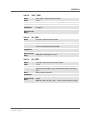
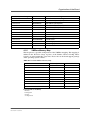
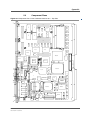
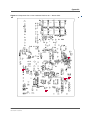
Figure 3. Position of Flash on Bottom Side of A11
C251
NR88
C3
C118
C86
IC56
C279
C447
C156
C154
C446
C328
C31 C161 C269
IC60
C18
C101
C102
C122
IC61
R1006
IC62
C250
C147
C68 C162 C37
C281
NR155
C264
C280
C4
C173
C329
C57
C348
C143
NR156
C158 C30
C350
C58
C193
C190
R14
R106
C164 C39
C274
C191 C209
C266
C27
C265 R123
C26
C40
C275
C41
C276
NR38
C48
C141
C25
C149
C49
C121
IC63
C70
C268
C28
C56
C453
C50
C23
NR157
NR158
C59
C263
C462
C112
C38 C165 C273
C172
C293
C74
C61
C142
C272
C270
C160 C32
C63
C330
C208
C148
R182
C454
C69
C319
C171
C62
C24
C248
C352
R13
C192
C17
C87
C215
C75
C267
C159 C29
R166
C463
C60
C271
C377
R138
L16
C455
C163 C36
C67
C370
C169
IC57
C194
R105
C177
C327
C378
R1007
C120
IC58
C157
C119
C320
C278
C155
IC59
R134
R137
C21
C195
C117
R167
C448
C214
C19
C22
R164
L15
R136
C136
C145
C20
C135
C326
C146
C249
R168
C170
C456
C301
R135
C322
C353
C464
NR32
C166
C167
C2
R59
C73
NR124
C203
C168
C277
NR24
C212
C84
C355
NR25
C144
C380
R180
03
R1003
C51
R1002
C44
C379
C213
C9
C189
R55
C71
R58
C72
C100
C349 R1011
C247
R1010 R1009 R1008 C292
NR45 C246
C347
R91
C302
C300
C96
NR14
NR57
C450
C442
C449
C441
NR1
C198
R125
R193
R124
NR84
2.5.4
R181
R188
R23
C34
C65 C125 C200
C324
C76
C131 NR154 NR52
C332
C5
C334
R145
R143
C199
C197
C420 R74
EEPROM
The A11 has a 4-kbit serial EEPROM for factory data.
MEN Mikro Elektronik GmbH
20A011-00 E4 - 2004-04-20
24
Functional Description
2.6
Ethernet Interface
The Ethernet interface of the A11 supports both 10Mbit/s and 100Mbit/s as well as
full-duplex operation and autonegotiation.
!
Note: The unique Ethernet address is set at the factory and should not be changed.
Any attempt to change this address may create node or bus contention and
thereby render the board inoperable. A label on the bottom side of the A11
gives the set Ethernet address.
2.6.1
Connection
A standard RJ45 connector is available at the front panel for connection to 10BaseT or 100Base-TX network environments. It is not necessary to switch between the
two configurations!
The pin assignment corresponds to the Ethernet specification IEEE802.3.
Connector types:
• Modular 8/8-pin mounting jack according to FCC68
• Mating connector:
Modular 8/8-pin plug according to FCC68
Table 3. Pin Assignment of the 8-pin RJ45 Ethernet 10Base-T/100Base-T
Connector
1
8
1
TX+
2
TX-
3
RX+
4
-
5
-
6
RX-
7
-
8
-
Table 4. Signal Mnemonics of the Ethernet 10Base-T/100Base-T Connector
Signal
Direction
Function
RX+/-
in
Differential pair of receive data lines
TX+/-
out
Differential pair of transmit data lines
The A11 also features a 10Base-5 interface for rear I/O via a rear I/O adapter at
VMEbus P2. (See also Chapter 2.21.2.3 Connecting a Rear I/O Adapter to P2 on
page 54 and MEN’s website for available adapters.)
MEN Mikro Elektronik GmbH
20A011-00 E4 - 2004-04-20
25
Functional Description
2.6.2
General
Ethernet is a local-area network (LAN) protocol developed by Xerox Corporation in
cooperation with DEC and Intel in 1976. Ethernet uses a bus or star topology and
supports data transfer rates of 100Mbps and more. The Ethernet specification served
as the basis for the IEEE 802.3 standard, which specifies the physical and lower
software layers. Ethernet uses the CSMA/CD access method to handle simultaneous
demands. It is one of the most widely implemented LAN standards.
Ethernet networks provide high-speed data exchange in areas that require
economical connection to a local communication medium carrying bursty traffic at
high-peak data rates.
A classic Ethernet system consists of a backbone cable and connecting hardware
(e.g. transceivers), which links the controllers of the individual stations via
transceiver (transmitter-receiver) cables to this backbone cable and thus permits
communication between the stations.
2.6.3
10Base-5
The yellow 10Base-5 thick-wire AUI line is the original type of Ethernet cable. The
simplest configuration is to connect the AUI connector of each station to this yellow
cable using a transceiver line and a transceiver. An Ethernet cable like this must not
be longer than 500m, and may have a maximum of 100 transceivers. The distance
between two transceivers must be at least 2.5m.
A transceiver contains the transmit and receive logic. It ensures regeneration-free
data transfers up to 500m cable length and carries out collision detection and carrier
sensing. Another task is electrical isolation between the station and the thick-wire
cable. The transceiver is supplied by the station via the transceiver cable. There are
also mini-transceivers that can be plugged directly to the AUI connector of the
Ethernet device.
The thick-wire cable must be electrically terminated by a 50-Ω termination resistor.
The line must only be grounded at one end (not at both).
2.6.4
10Base-T
10Base-T is one of several adaptations of the Ethernet (IEEE 802.3) standard for
Local Area Networks (LANs). The 10Base-T standard (also called Twisted Pair
Ethernet) uses a twisted-pair cable with maximum lengths of 100 meters. The cable
is thinner and more flexible than the coaxial cable used for the 10Base-2 or
10Base-5 standards. Since it is also cheaper, it is the preferable solution for costsensitive applications.
Cables in the 10Base-T system connect with RJ45 connectors. A star topology is
common with 12 or more computers connected directly to a hub or concentrator.
The 10Base-T system operates at 10Mbps and uses baseband transmission methods.
MEN Mikro Elektronik GmbH
20A011-00 E4 - 2004-04-20
26
Functional Description
2.6.5
100Base-T
The 100Base-T networking standard supports data transfer rates up to 100Mbps.
100Base-T is actually based on the older Ethernet standard. Because it is 10 times
faster than Ethernet, it is often referred to as Fast Ethernet. Officially, the 100Base-T
standard is IEEE 802.3µ.
Like Ethernet, 100Base-T is based on the CSMA/CD LAN access method. There
are several different cabling schemes that can be used with 100Base-T, including:
• 100Base-TX:
• 100Base-T4:
• 100Base-FX:
MEN Mikro Elektronik GmbH
20A011-00 E4 - 2004-04-20
two pairs of high-quality twisted-pair wires
four pairs of normal-quality twisted-pair wires
fiber optic cables
27
Functional Description
2.7
SCSI Interface
The SCSI interface of the A11 is based on the SYM53C895 device and supports
wide (16-bit) and narrow (8-bit) configurations. It supports Ultra and Ultra2 SCSI
modes with a maximum transfer rate of 80MB/s. Signaling interfaces supported are
either SE (single-ended) or LVD (low voltage differential).
The A11 provides active termination that can be changed between SE and LVD
mode. Mixed operation of SE and LVD is not possible.
You can set SE or LVD mode through MENMON.
2.7.1
Connection
A standard VHDCI connector is provided at the front panel.
Connector types:
• 68-pin shielded half-pitch D-Sub receptacle, very high density (VHD)
• Mating connector:
68-pin half-pitch D-Sub plug, VHD
Table 5. Signal Mnemonics for SCSI Interface
Signal
Direction
Function
DIFFSENSE
in/out
Differential mode sense
GND
-
Ground
SACK+/-
in/out
Acknowledge, differential pair
SATN+/-
in/out
Attention, differential pair
SBSY+/-
in/out
Busy, differential pair
SCD+/-
in/out
Command/data, differential pair
SD+/-[0..15]
in/out
Data lines, differential pairs
SDP+/-[0..1]
in/out
Data parity, differential pairs
SIO+/-
in/out
Input/output, differential pair
SMSG+/-
in/out
Message, differential pair
SREQ+/-
in/out
Request, differential pair
SRST+/-
in/out
Bus reset, differential pair
SSEL+/-
in/out
Select device, differential pair
TERMPWR
-
Termination power
The A11 also supports two SCSI interfaces for rear I/O via a rear I/O adapter at
VMEbus P2. (See also Chapter 2.21.2.3 Connecting a Rear I/O Adapter to P2 on
page 54 and MEN’s website for available adapters.)
!
Please note that front connection allows SE or LVD mode, while rear connection
only permits SE mode. If you have connected a device at the rear, you can use only
SE mode also at the front.
MEN Mikro Elektronik GmbH
20A011-00 E4 - 2004-04-20
28
Functional Description
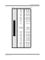
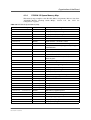
Table 6. Pin Assignment of the 68-pin VHDCI SCSI Connector
68
35
MEN Mikro Elektronik GmbH
20A011-00 E4 - 2004-04-20
34
1
68
SD-[11]
34
SD+/GND[11]
67
SD-[10]
33
SD+/GND[10]
66
SD-[9]
32
SD+/GND[9]
65
SD-[8]
31
SD+/GND[8]
64
SIO-
30
SIO+/GND
63
SREQ-
29
SREQ+/GND
62
SCD-
28
SCD+/GND
61
SSEL-
27
SSEL+/GND
60
SMSG-
26
SMSG+/GND
59
SRST-
25
SRST+/GND
58
SACK-
24
SACK+/GND
57
SBSY-
23
SBSY+/GND
56
-
22
-
55
SATN-
21
SATN+/GND
54
-
20
-
53
-
19
-
52
TERMPWR
18
TERMPWR
51
TERMPWR
17
TERMPWR
50
-
16
DIFFSENSE
49
-
15
-
48
SDP-[0]
47
SD-[7]
13
SD+/GND[7]
46
SD-[6]
12
SD+/GND[6]
45
SD-[5]
11
SD+/GND[5]
44
SD-[4]
10
SD+/GND[4]
43
SD-[3]
9
SD+/GND[3]
42
SD-[2]
8
SD+/GND[2]
41
SD-[1]
7
SD+/GND[1]
40
SD-[0]
6
SD+/GND[0]
39
SDP-[1]
5
SDP+/GND[1]
38
SD-[15]
4
SD+/GND[15]
37
SD-[14]
3
SD+/GND[14]
36
SD-[13]
2
SD+/GND[13]
35
SD-[12]
1
SD+/GND[12]
14 SDP+/GND[0]
29
Functional Description
2.7.2
General
SCSI (Small Computer System Interface) has a long history in the relatively short
period of the computing industry. SCSI's origins date back to the Selector Channel
on IBM-360 systems. It was first scaled down to be a universal, intelligent disk drive
interface. SCSI became an ANSI standard in 1986.
Over the last years since it became an official industry standard, SCSI has grown
and evolved to keep pace with the demands of the most sophisticated systems. The
standard recognizes magnetic disk and tape drives, various types of optical disk
drives, printers, scanners, processors, communications devices, medium changers,
and more.
The standard has also evolved to take advantage of newer hardware and more
intelligent controllers; caching is recognized; intelligent command queuing is
accommodated. There are also provisions for intelligent self-testing by the
peripheral. The data path has been widened and transfer speeds have been increased
to keep pace with system requirements.
2.7.2.1
SCSI Versions
SCSI drives have an integrated SCSI controller. There are different sorts of SCSI
interfaces, differing in the type of data transfer. SCSI signals can be transmitted
either via an 8-bit (narrow) or a 16-bit (wide SCSI) bus. It is possible to connect up
to 7 drives to an 8-bit bus, and up to 15 drives to a 16-bit bus. Both bus widths can
be configured as single-ended or differential SCSI. Single-ended SCSI transmits the
signals only via one line, differential SCSI via two lines. This makes four different
interface configurations: single-ended with 8 bits, single-ended with 16 bits,
differential with 8 bits and differential with 16 bits. When choosing a subsystem you
must make sure that the SCSI interface of the host adapter corresponds to the drive.
In general, 8-bit devices can be connected to a 16-bit bus. However, you must
consider a number of special rules for configuration. In addition, performance of the
16-bit bus is limited to that of an 8-bit bus, so that there may be transfer problems on
the SCSI bus. If both single-ended and differential versions are operated on the bus
at the same time, this can lead to damage to the disk drive and the controller. If the
controller and disk drive interfaces do not match, a single-differential-ended
converter must be used. In this case, however, impedances and signal timing on the
SCSI bus may be changed, which in turn can result in problems.
Single-Ended (SE) and Differential (DI) SCSI
With single-ended (SE) SCSI each signal is transferred on one line, with differential
(DI) SCSI on two lines. The advantages of differential SCSI lie in longer cable
lengths (25m instead of 6m) and greater immunity to interference. Disadvantages
are higher costs for disk drives and host adapter. Combining SE SCSI and DI SCSI
drives on one bus is not possible without special converters.
Low Voltage Differential (LVD) SCSI
LVD is a differential bus technology that combines much of the bus length, noise
immunity and performance benefits of conventional DI SCSI with the power
consumption and cost of SE SCSI interfaces. Power consumption of LVD devices is
reduced compared to a conventional differential bus through improvements in
receiver design that permit reductions in steady-state current consumption and
signaling voltage.
MEN Mikro Elektronik GmbH
20A011-00 E4 - 2004-04-20
30
Functional Description
Because of this lower power consumption, LVD drivers can be integrated into the
silicon interface chips thus eliminating the signal skew, real estate and cost
associated with separate differential components. What's more, by taking advantage
of the latest CMOS processes, dual-mode LVD cells can be designed that support
either single-ended or differential operation. Selection of operational mode (SE or
DI) by the device is automatic and is done without the use of jumpers. Because of
this compatibility, the cost of SCSI devices with LVD silicon will not differ
appreciably from comparable single-ended drives.
Synchronous and Asynchronous Data Transfer
SCSI data transfer can be asynchronous or synchronous, the latter being faster. With
asynchronous data transfer, each byte is sent and confirmed separately, whereas
with synchronous transfer several bytes are sent at once and then confirmed as one.
This makes for smaller overhead and higher transfer rates. Generally, all peripherals
can operate asynchronously. Synchronous drives or controllers perform a handshake
before data exchange, i.e. they check whether the communication partner is capable
of synchronous transfer. After handshaking, they automatically use the appropriate
data transfer method.
2.7.2.2
SCSI Cables
In order to allow trouble-free data transfer, some basic aspects must be considered
when choosing an SCSI cable.
The SCSI cables must be specified according to UL (Underwriters’ Laboratories)
and CSA (Canadian Standard Association). The individual wires of the cable must
be made of copper (or better: tin-plated copper). they must be twisted in pairs, and
in addition the cable should be twisted over a length of max. 1m. The complete
cable needs double screening.
If several peripherals are connected to a SCSI bus, the individual connection cables
should be as short as possible and ideally have the same length. This reduces
susceptibility to interference.
With wide SCSI, data transfer is done with 16 instead of 8 bits; the lines available in
the 50-pin SCSI cable are not enough. Therefore, wide SCSI uses special 68-line
cables for both single-ended wide SCSI and differential wide SCSI.
Table 7. Overview of SCSI Types, Maximum Bus Widths, Throughput and Line Lengths
Type
Bus Width Throughput
SE Line
DI Line
LVD Line
Max. Devices
SCSI-1
8 bits
5 MB/s
6m
25m
12m
8
Fast SCSI
8 bits
10 MB/s
3m
25m
12m
8
Fast Wide SCSI
16 bits
20 MB/s
3m
25m
12m
16
Ultra SCSI
8 bits
20 MB/s
1.5m
25m
12m
8
Ultra SCSI
8 bits
20 MB/s
3m
-
-
4
Wide Ultra SCSI
16 bits
40 MB/s
-
25m
12m
16
Wide Ultra SCSI
16 bits
40 MB/s
1.5m
-
-
8
Wide Ultra SCSI
16 bits
40 MB/s
3m
-
-
4
Ultra2 SCSI
8 bits
40 MB/s
-
-
12m
8
Wide Ultra2 SCSI
16 bits
80 MB/s
-
-
12m
16
MEN Mikro Elektronik GmbH
20A011-00 E4 - 2004-04-20
31
Functional Description
2.7.3
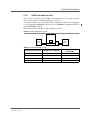
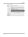
SCSI Termination on A11
The A11 can be located in the "middle" of the SCSI bus or at its end. You must
make sure the board is terminated properly for any case.
As mentioned above, the A11 provides active termination, which can be configured
as needed through MENMON. Please refer to MENMON command H EE for
detailed MENMON settings.
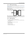
The following figure and table clarify termination on A11:
Figure 4. SCSI Termination on A11
A11
Term.
SCSI
Device
AD39
SCSI
Device
Table 8. SCSI Termination on A11
P2 Rear I/O via Adapter
Not connected
Not connected
Active termination on
SCSI device connected
Not connected
Active termination on
Not connected
SCSI device connected
Active termination on
SCSI device connected
SCSI device connected
Active termination off
MEN Mikro Elektronik GmbH
20A011-00 E4 - 2004-04-20
Applicable SCSI
Termination
68-pin Front Connector
32
Functional Description
2.8
PCI Expansion
The A11’s PCI expansion slot allows for various expansions at the PCI bus, e.g.
using expansion cards for PMC or PC•MIP mezzanines. Different expansion boards
are in preparation.
Connector types:
• 114-pin matched impedance receptacle connector, MICTOR .025 [0.64] centerline
• Mating connector:
114-pin matched impedance plug connector, MICTOR .025 [0.64] centerline
MEN Mikro Elektronik GmbH
20A011-00 E4 - 2004-04-20
33
Functional Description
Table 9. Pin Assignment of the 114-pin PCI Expansion Connector
77
113
MEN Mikro Elektronik GmbH
20A011-00 E4 - 2004-04-20
40
78
114
3
CLK
4
INTA#
5
GND
6
INTB#
7
PURST#
8
INTC#
9
HRESET#
10
INTD#
11
TDO
12
TDI
13
TMS
14
TCK
15
TRST#
16
PRESENT#
17
GNT#
18
REQ#
3.3V
19
+12V
20
-12V
21
PERR#
22
SERR#
23
LOCK#
24
SDONE#
25
DEVSEL#
26
SBO#
27
GND
28
GND
29
TRDY#
30
IRDY#
31
STOP#
32
FRAME#
33
GND
34
GND
35
ACK64#
36
Reserved
37
REQ64#
38
Reserved
39
PAR
40
RST#
41
C/BE1#
42
C/BE0#
43
C/BE3#
44
C/BE2#
45
AD1
46
AD0
47
AD3
48
AD2
49
AD5
50
AD4
51
AD7
52
AD6
53
AD9
54
AD8
55
AD11
56
AD10
57
AD13
58
AD12
59
AD15
60
AD14
61
AD17
62
AD16
63
AD19
64
AD18
65
AD21
66
AD20
67
AD23
68
AD22
69
AD25
70
AD24
71
AD27
72
AD26
73
AD29
74
AD28
75
AD31
76
AD30
77..113
Reserved
78..114
Reserved
+5V
39
2
2
GND
1
3.3V
GND
1
34
Functional Description
2.9
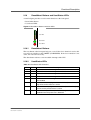
PC•MIP Slots
The A11 has two PC•MIP slots for Type-I and Type-II modules. Interfacing
between the local 5V PCI bus and the 3.3V PC•MIP PCI bus is done using a
DEC21150 PCI-to-PCI bridge.
The PC•MIP slots enable the user to add functionality to the A11 CPU board, from
graphics to process I/O.
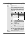
2.9.1
Installing PC•MIPs
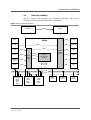
Perform the following steps to install a PC•MIP:
If you want to install a Type-II PC•MIP (with front connector), you must
remove the blank bezel at the front panel of the A11 first:
Remove the respective bezel keeper by loosening the keeper screw at the bottom side of the A11. (See Figure 1, Map of the Board - Front Panel and Top
View, on page 16).
Place the finished bezel supplied with your PC•MIP in the front panel cut-out
and reinstall the bezel keeper.
Place the PC•MIP on the target slot of the A11, aligning the three connectors
(P1/J1, P2/J2, P3/J3) and the two standoffs.
If you are installing a Type-II PC•MIP, carefully put the module’s front connector through the finished bezel, holding the module at a 45° angle.
Screw the PC•MIP to the carrier by alternately tightening the two captive
screws on the label side of the PC•MIP. The module will be "injected" safely.
Figure 5. Installation of a PC•MIP
System Front
Panel
Captive Screw
J3
P3
PC•MIP Front
I/O Connector
(Type II module)
PC•MIP (Type I or II)
Standoff
J1
P1
Captive Screw
Standoff
Carrier Board
Keeper
Keeper Screw
To deinstall PC•MIPs from the carrier board, just loosen the appropriate screws at
the label side of the PC•MIP. The injector/ejector system will "eject" the PC•MIP.
MEN Mikro Elektronik GmbH
20A011-00 E4 - 2004-04-20
35
Functional Description
2.9.2
PC•MIP Connectors
PC•MIP modules connect to the A11’s PCI bus via the two identical 64-pin
connectors P1 and P2. The connector layout is fully compatible to the PC•MIP
specification and will not be repeated here.
!
Although the A11 has a third, identical 64-pin connector (P3), it does not support
rear I/O connection.
Connector types of P1, P2 and P3:
• 64-pin SMT plug connector according to IEEE P1386, e. g. Molex 71436-0864
• Mating connector:
64-pin SMT receptacle connector according to IEEE P1386, e. g. Molex 714391864
MEN Mikro Elektronik GmbH
20A011-00 E4 - 2004-04-20
36
Functional Description
2.10
CompactFlash
CompactFlash is a standard for small form factor ATA Flash drives. It is electrically
compatible to the PC Card 1995 and PC Card ATA standards.
The CompactFlash standard is supported by industry’s leading vendors of Flash
cards.
You can use CompactFlash cards with the A11 through the AD35 adapter, which is
accessible at the front panel. The adapter is connected using a board-to-board
connector. The AD35 configures CompactFlash cards in a True IDE Mode of
operation.
!
Note: Removing and reinserting a CompactFlash card while the host computer’s
power is on might damage the IDE controller or the storage card. The least
that will happen is a reconfiguration of the CompactFlash card to PC Card
ATA mode from the original True IDE Mode.
2.10.1
Installing CompactFlash
The A11 is shipped without a CompactFlash card installed. To install
CompactFlash, please stick to the following procedure.
Figure 6. CompactFlash Card
Ejector
CompactFlash
Card
Power down your system.
Insert the card carefully as indicated by the arrow on top of the card, making
sure that all the contacts are aligned properly and the card is firmly in the card
socket.
Remove the CompactFlash card by pressing the ejector.
Observe manufacturer notes on usage of the Flash cards.
2.10.2
Supported CompactFlash Cards
The A11 supports standard CompactFlash cards.
For CompactFlash cards available from MEN see MEN’s website.
MEN Mikro Elektronik GmbH
20A011-00 E4 - 2004-04-20
37
Functional Description
2.11
Keyboard/Mouse
The built-in PS2/AT keyboard and PS2 mouse controller of the M1543 is connected
to a single mini DIN connector at the front panel.
Note: For the connection of both devices a special cable is necessary. MEN offers a
Y-cable for easy connection of a keyboard and mouse. For ordering numbers
please refer to MEN’s website.
A 6-pin mini DIN connector is provided to connect a standard PS/2 keyboard.
Connector types:
• 6-pin circular mini DIN receptacle
• Mating connector:
6-pin circular mini DIN plug, available for soldering and crimp connection
Table 10. Pin Assignment of the 6-Pin Mini DIN Keyboard/Mouse Connector
4
4 6
2
1
KB_VCC
2
MSEDAT
6
MSECLK
1
KBDAT
5
KBCLK
3 5
3
KB_GND
Table 11. Signal Mnemonics for Keyboard/Mouse Interface
Signal
Function
KB_GND
-
Keyboard logic ground
KB_VCC
-
Keyboard +5V supply, max. DC current 200mA
KBCLK
out
Keyboard clock
KBDAT
out
Keyboard data
MSECLKDAT
out
Mouse clock
MSEDAT
out
Mouse data
MEN Mikro Elektronik GmbH
20A011-00 E4 - 2004-04-20
Direction
38
Functional Description
2.12
Serial Ports COM1/COM2
The A11 provides two high-performance 16550 compatible UARTs with 16-byte
send/receive FIFOs and programmable baud rate generator. You can set the baud
rate through MENMON.
2.12.1
Connection
The serial ports COM1 and COM2 are accessible at the front panel as well as on a
rear I/O adapter. The A11 has two different pairs of physical RS232 transceivers.
You can change configuration of the receiver for front or rear I/O through
MENMON command EE. Please note that the transmitters are always enabled.
A11 provides two 9-pin micro D-Sub connectors at the front panel. Their pin
assignment is PC-compatible.
Connector types:
• 9-pin micro D-Sub socket connector with screw locking, ITT Cannon MDSM9SC-Z11-VS1
• Mating connector:
9-pin connector with locking post, ITT Cannon MDSM-9PE-Z10-VR
Table 12. Pin Assignment of the 9-pin micro D-Sub COM1/COM2 Plug Connectors
(RS232)
6
9
1
5
6
DSR
1
DCD
7
RTS
2
RXD
8
CTS
3
TXD
9
RI
4
DTR
5
GND
Table 13. Signal Mnemonics for RS232 Serial Ports COM1/COM2
Signal
Direction
Function
CTS
in
Clear to send
DCD
in
Data carrier detect
DSR
in
Data set ready
DTR
out
Data terminal ready
GND
-
Logic ground
RI
in
Ring indicator
RTS
out
Request to send
RXD
in
Receive data
TXD
out
Transmit data
The A11 also supports COM1 and COM2 at VMEbus P2 for rear I/O via a rear I/O
adapter. The signal level is fixed to TTL at the rear. This allows flexible line
interface configuration using serial interface (SA) adapters. (See also Chapter
2.21.2.3 Connecting a Rear I/O Adapter to P2 on page 54 and MEN’s website for
available rear I/O and SA adapters.)
MEN Mikro Elektronik GmbH
20A011-00 E4 - 2004-04-20
39
Functional Description
2.13
Asynchronous/Synchronous Serial Ports COM3/COM4
The A11 uses the Zilog Z85230 ESCC (Enhanced Serial Communications
Controller) to implement two serial communications interfaces—COM3 and
COM4. COM3 is prepared for asynchronous protocols and COM4 for synchronous
protocols such as SDLC or HDLC. The ports are accessible only via VMEbus P2
via a rear I/O adapter. The hardware supports asynchronous serial baud rates of
110 bytes/s up to 38.4 KB/s.
For synchronous operation of COM4 you need to specify the clock signaling for
transmitter and receiver. With the help of three jumpers you can select the source of
the synchrounous clock.
Figure 7. COM4 Clock Signals — Principle
A11
AD39
P5
TRxC*
D
R
1
2
3
TRxC4
P4
D
RTxC*
R
1
2
3
RTxC4
Jumpers
1
2
3
4
5
6
RTXC
RRXC
TTXC
You can configure the clock signals using jumpers:
Table 14. Configuring Clock Signals for COM4
Clock Signal
Transmit clock (TRxC#)
Receive clock (RTxC#)
MEN Mikro Elektronik GmbH
20A011-00 E4 - 2004-04-20
A11 Source
External Source
P5
P7
P6
P5
1 2 3
1 2
1 2
1 2 3
P7
P6
1 2
1 2
P4
P4
1 2 3
1 2 3
40
Functional Description
Figure 8. Jumpers for Clock Selection for COM4 (Default Setting: all jumpers
removed)
Injectors/Ejectors
with Threaded
Standoffs and
Captive Screws
P2
P3
PC•MIP slot 1
SO-DIMM
DRAM
Socket
P1
VMEbus P1
Finished Bezel
of PC•MIP I/O
Connector
P2
P3
PC•MIP slot 2
PC•MIP
Keeper Screw
(solder side)
P1
Ethernet
10Base-T/100Base-T
Keyboard/Mouse
PCI
Bridge
PowerPC
Processor
Core
Tundra
Universe II
VMEbus
Controller
User LEDs
COM2
Abort Button
Reset Button
SCSI
Interface
CompactFlash
Card Slot
IEEE
1149.1/
COP Test
Interface
VMEbus P2
COM1
PCI Extension Slot
PC•MIP Bezel
Keepers
Southbridge
Floppy Disk
Drive Interface
P4 P5 P7 P6
User-defined Hex Switch
Configuration Jumpers
P4
P5
P7
P6
1 2 3
1 2 3
1 2
1 2
See Chapter 2.21.2.3 Connecting a Rear I/O Adapter to P2 on page 54 and MEN’s
website for available rear I/O adapters.
2.14
Enhanced Parallel Port
The enhanced parallel port of the A11 is connected to the VMEbus P2 connector for
rear I/O via a rear I/O adapter. It supports ECP, EPP, PS/2, SPP and 1284
compliance. The port includes a protection circuit against damage caused when a
printer is powered up or operated at higher voltages.
See Chapter 2.21.2.3 Connecting a Rear I/O Adapter to P2 on page 54 and MEN’s
website for available rear I/O adapters.
MEN Mikro Elektronik GmbH
20A011-00 E4 - 2004-04-20
41
Functional Description
2.15
Floppy Disk Controller
The floppy disk controller supports up to 2.88 MB formatted floppy disk drives. It is
compatible with 82077 and supports 16-byte data FIFOs. It includes a highperformance internal data separator and supports standard 1 Mbit/s, 500 Kbit/s,
300 Kbit/s and 250 Kbit/s data transfer rates.
All standard PC modes of 3.5" floppy disk drives (720KB/1.2MB/1.44MB) are
implemented. Drives A and B are swapable.
Connector types:
• 26-pin ZIF/SMT receptacle, 1mm pitch, for FPC/FFC connection
• mating connector:
26-pin ZIF plug, 1mm pitch, for FPC/FFC connection
Table 15. Pin Assignment of 26-pin ZIF Floppy Disk Drive Connector
1
26
MEN Mikro Elektronik GmbH
20A011-00 E4 - 2004-04-20
1
+5V
2
INDEX#
3
+5V
4
SEL0#
5
+5V
6
CHANGE#
7
-
8
-
9
DENSEL
10
MOTON#
11
-
12
DIR#
13
-
14
STEP#
15
GND
16
WDATA#
17
GND
18
WGATE#
19
GND
20
TRK0#
21
GND
22
WP#
23
GND
24
RDATA#
25
GND
26
HDSEL#
42
Functional Description
Table 16. Signal Mnemonics for Floppy Disk Drive Connector
Signal
Function
+5V
-
+5V power supply, current-limited to 1.5A by a fuse
CHANGE#
in
Disk change
DENSEL
out
Density select
DIR#
out
Direction
GND
-
Digital ground
HDSEL#
out
Head select
INDEX#
in
Index
MOTON#
out
Motor on
RDATA#
in
Read data
SEL0#
out
Drive select 0
STEP#
out
Step
TRK0#
in
Track 0
WDATA#
out
Write data
WGATE#
out
Write gate
WP#
in
Write protect
MEN Mikro Elektronik GmbH
20A011-00 E4 - 2004-04-20
Direction
43
Functional Description
2.16
Hardware Monitor
The LM78 hardware monitor is used for voltage and temperature management.
Several supply voltages can be monitored. When the programmed limits are
exceeded, the monitor will generate an interrupt. Together with suitable software,
you can use the hardware monitor to create voltage protocols, for example.
The on-board temperature is measured continuously.
Table 17. Hardware Monitor Channels
Channel
Voltage
0
+5V
1
+3.3V
2
CPU core voltage
3
+12V
4
Battery voltage from VMEbus
5
-12V
2.17
Timekeeper, NVRAM and Watchdog
The A11 includes the M48T59Y 64Kbit timekeeper NVRAM with watchdog. A
snaphat top with battery and oscillator guarantees a typical data retention of 10
years at 25°C. The M48T59 checks its battery voltage at power-up. An internal
control bit is set at power-up if the battery voltage is below 2.5V (typical).
The NVRAM is organized as an 8K x 8bit SRAM.
The timeout period of the watchdog timer is programmable from 1/16 s to 4 s in
four steps.
2.18
Counter/Timer CIO Z8536
The Z8536 CIO is a counter/timer and parallel I/O unit which is used to provide the
modem control lines which are not provided by the Z85230 ESCC.
In VME64 applications the geographic address pins may be read at the I/O pins.
Four ports are used for the software implementation of an SMB controller for serial
devices such as LM78, 4-Kbit EEPROM or clock generation.
Three independent 16-bit counter timers are free for user implementations.
MEN Mikro Elektronik GmbH
20A011-00 E4 - 2004-04-20
44
Functional Description
2.19
Reset/Abort Buttons and User/Status LEDs
A small adapter provides several control functions at the front panel:
• Reset/Abort button
• User/status LEDs.
Figure 9. Reset/Abort Buttons and User LEDs
0
1
2
3
4
5
6
7
User LEDs
Abort Button
Reset Button
2.19.1
Reset/Abort Buttons
The reset button at the front panel triggers a reset. If the slot-1 function is active, this
reset will act globally for the VMEbus (SYSRESET#). If the slot-1 function is not
active, the reset will act locally.
The abort button activates a non-maskable interrupt of the CPU.
2.19.2
User/Status LEDs
Table 18. User/Status LED Functions
LED
Description
0
Green
User-defined function through M1543 GPO 23
1
Green
User-defined function through M1543 GPO 22
2
Green
User-defined function through M1543 GPO 20
3
Green
User-defined function through M1543 GPO 9
4
Yellow
VMEbus: slot-1 function; lights when VMEbus slot-1 functions
are enabled
5
Yellow
PCI bus: PCI activity; lights when the IRDY# (Initiator Ready)
signal line on the PCI bus is active
6
Yellow
CPU: CPU activity; lights when the DBB# (Data Bus Busy) signal line on the processor bus is active
7
Red
CHS: checkstop; driven by the PowerPC; lights when a halt
condition from the processor is detected
MEN Mikro Elektronik GmbH
20A011-00 E4 - 2004-04-20
Color
45
Functional Description
2.20
User-Defined Hex Switch
The A11 provides a rotary hex switch for operating system requirements and user
applications. Please refer to the corresponding software manual for the
implemention.
Figure 10. Position of Hex Switch
VMEbus P1
SO-DIMM
DRAM
Socket
P1
P2
P3
PC•MIP slot 2
PC•MIP
Keeper Screw
(solder side)
P1
Ethernet
10Base-T/100Base-T
Keyboard/Mouse
PCI
Bridge
PowerPC
Processor
Core
Tundra
Universe II
VMEbus
Controller
User LEDs
COM2
Abort Button
Reset Button
SCSI
Interface
CompactFlash
Card Slot
IEEE
1149.1/
COP Test
Interface
VMEbus P2
COM1
PCI Extension Slot
PC•MIP Bezel
Keepers
Southbridge
Floppy Disk
Drive Interface
P4 P5 P7 P6
User-defined Hex Switch
MEN Mikro Elektronik GmbH
20A011-00 E4 - 2004-04-20
Configuration Jumpers
46
Functional Description
2.21
VMEbus Interface
The A11's VMEbus interface conforms to the VME64 specification. It has the
following features:
• Tundra Universe II VMEbus chip
• Slot-1 functionality
• Wide range of VMEbus address and data transfer modes
- A32/A24/A16 master and slave (no A64 or A40)
- D64/D32/D16/D08 master and slave (no MD32)
- MBLT, BLT, ADOH, RMW, LOCK, location monitors
• Interrupt handler: 7-level
• Interrupter: 7-level
2.21.1
Implementation on the Board
2.21.1.1 VMEbus Master
The Tundra Universe II becomes VMEbus master when it is requested by the PCI
bus. In this case it acts as a PCI target device.
The A11 supports all addressing and data transfer modes documented in the VME64
specification (except A64) including read-modify-write and address-only cycles.
The mapping of the PCI address spaces to the VMEbus address areas depends on
software. Please refer to the board support package of the respective operating
system.
2.21.1.2 VMEbus Slave
The Tundra Universe II may be also configured for VMEbus slave capabillities. The
chip then works as a master to the local PCI bus.
2.21.1.3 VMEbus Interrupter
Interrupt generation is possible on all seven VMEbus levels. The interrupts are
generated fully under software control by setting the specific hardware registers.
Please refer to the Tundra Universe II user manual for a detailed description.
MEN Mikro Elektronik GmbH
20A011-00 E4 - 2004-04-20
47
Functional Description
2.21.1.4 VMEbus Interrupt Handler
The A11 is able to handle all seven VMEbus interrupts. The interrupts may be
masked and enabled in the Tundra Universe II register set (cf. Chapter 4.2 Interrupt
Handling on page 94).
The Tundra Universe II generates a single PCI interrupt with the LINT0 on the
INTB line. This interrupt is routed inside the M1543 interrupt controller to a
dedicated ISA interrupt.
Figure 11. VMEbus Interrupts
IRQ7
IRQ6
LINT0
Tundra
Universe II
IRQ5
Interrupt
Handler
IRQ3
IRQ4
VMEbus
IRQ2
IRQ1
When receiving an interrupt from the VMEbus the Tundra Universe II first
generates an IACK cycle to the VMEbus. After completion of the cycle the interrupt
to the PCI bus will be asserted and the local CPU may read the interrupt vector
number from the Tundra Universe II registers.
2.21.1.5 VMEbus Utility Bus
The A11 supports all VMEbus utility functions such as:
• 4-level bus arbitration with fixed priority (PRI), single level arbitration (SGL) or
round-robin (RRS) mode
• Slot-1 detection
• Programmable VMEbus timeout from 16..1024µs
• System clock driver
• IACK daisy chain driver
• System reset generation
• SYSFAIL# and ACFAIL# monitor
MEN Mikro Elektronik GmbH
20A011-00 E4 - 2004-04-20
48
Functional Description
2.21.2
Connection
Connector types P1/P2 (3-row VMEbus):
• Type-C 96-pin plug connector according to DIN41612/MIL-C-55302/IEC603-2
• Mating connector:
Type-C 96-pin receptacle according to DIN41612/MIL-C-55302/IEC603-2
Connector types P1/P2 (5-row VMEbus):
• 160-pin, 5-row plug, performance level according to DIN41612, part 5
• Mating connector:
160-pin, 5-row receptacle, performance level according to DIN41612, part 5
!
Note: Connector rows Z and D are only present with 5-row VMEbus models of the
A11!
MEN Mikro Elektronik GmbH
20A011-00 E4 - 2004-04-20
49
Functional Description
2.21.2.1 Pin Assignment of P1
The pin assignment of P1 conforms to the VME64 specification VITA 1-1994 and
VME64 Extensions Draft Standard VITA 1.1-199x.
Table 19. Pin Assignment of the 5/3-Row, 96/160-Pin VMEbus Connector P1
Z A B CD
1
32
Z
A
B
C
D
1
-
D0
BBSY#
D8
-
2
GND
D1
BCLR#
D9
GND
3
-
D2
ACFAIL#
D10
-
4
GND
D3
BG0IN#
D11
-
5
-
D4
BG0OUT#
D12
-
6
GND
D5
BG1IN#
D13
-
7
-
D6
BG1OUT#
D14
-
8
GND
D7
BG2IN#
D15
-
9
-
GND
BG2OUT#
GND
GAP#
10
GND
SYSCLK
BG3IN#
SYSFAIL#
GA0#
11
-
GND
BG3OUT#
BERR#
GA1#
12
GND
DS1#
BR0#
SYSRESET#
-
13
-
DS0#
BR1#
LWORD#
GA2#
14
GND
WRITE#
BR2#
AM5
-
15
-
GND
BR3#
A23
GA3#
16
GND
DTACK#
AM0
A22
-
17
-
GND
AM1
A21
GA4#
18
GND
AS#
AM2
A20
-
19
-
GND
AM3
A19
-
20
GND
IACK#
GND
A18
-
21
-
IACKIN#
-
A17
-
22
GND
IACKOUT#
-
A16
-
23
-
AM4
GND
A15
-
24
GND
A7
IRQ7#
A14
-
25
-
A6
IRQ6#
A13
-
26
GND
A5
IRQ5#
A12
-
27
-
A4
IRQ4#
A11
-
28
GND
A3
IRQ3#
A10
-
29
-
A2
IRQ2#
A9
-
30
GND
A1
IRQ1#
A8
-
31
-
-12V
VSTBY
+12V
GND
32
GND
+5V
+5V
+5V
-
MEN Mikro Elektronik GmbH
20A011-00 E4 - 2004-04-20
50
Functional Description
2.21.2.2 Pin Assignment of P2
Table 20. Pin Assignment of the 5/3-Row, 96/160-Pin VMEbus Connector P2
Z A B CD
1
32
Z
A
B
C
D
1
SDB[8]#
SDB[0]#
+5V
ENC#
-
2
GND
SDB[1]#
GND
ENC
-
3
SDB[9]#
SDB[2]#
-
ENT#
-
4
GND
SDB[3]#
V_A[24]
ENT
-
5
SDB[10]#
SDB[4]#
V_A[25]
ENR#
-
6
GND
SDB[5]#
V_A[26]
ENR
-
7
SDB[11]#
SDB[6]#
V_A[27]
+12VLAN
-
8
GND
SDB[7]#
V_A[28]
PR_STR#
-
9
SDB[12]#
SDBP[0]
V_A[29]
PR_D[0]
-
10
GND
SATN#
V_A[30]
PR_D[1]
-
11
SDB[13]#
SBSY#
V_A[31]
PR_D[2]
-
12
GND
SACK#
GND
PR_D[3]
-
13
SDB[14]#
SRST#
+5V
PR_D[4]
-
14
GND
SMSG#
V_D[16]
PR_D[5]
-
15
SDB[15]#
SSEL#
V_D[17]
PR_D[6]
-
16
GND
SCD#
V_D[18]
PR_D[7]
-
17
SDBP[1]
SREQ#
V_D[19]
PR_ACK#
-
18
GND
SIO#
V_D[20]
PR_BSY
-
19
-
TxD3
V_D[21]
PR_PE
-
20
GND
RxD3
V_D[22]
PR_SLCT
-
21
-
RTS3
V_D[23]
PR_INIT#
-
22
GND
CTS3
GNV_D[
PR_ERR#
-
23
-
DTR3
V_D[24]
TxD1
-
24
GND
DCD3
V_D[25]
RxD1
-
25
-
TxD4
V_D[26]
RTS1
-
26
GND
RxD4
V_D[27]
CTS1
-
27
-
RTS4
V_D[28]
TxD2
-
28
GND
TRxC4
V_D[29]
RxD2
-
29
-
CTS4
V_D[30]
RTS2
-
30
GND
DTR4
V_D[31]
CTS2
-
31
-
DCD4
GND
TERMPWR
GND
32
GND
RTxC4
+5V
DIFFSENSE
-
Note: The pin assignment of P2 is compatible with Motorola’s MVME712M
transition module.
MEN Mikro Elektronik GmbH
20A011-00 E4 - 2004-04-20
51
Functional Description
Table 21. Signal Mnemonics of VMEbus Rear I/O Connector P2
COM1
SCSI
Parallel Port
Ethernet VMEbus Power Lines
Signal
Function
+5V
-
+5V power supply
+12V
-
+12V power supply
+12VLAN
-
+12V Ethernet power supply
GND
-
Digital ground
V_A[24:A31]
in
VMEbus address lines A24..A31
V_D[16:D31]
in/out
VMEbus data lines D16..D31
ENC/ENC#
in?
Collision
ENR/ENR#
in
Receive lines
ENT/ENT#
out
Transmit lines
PR_ACK#
in
Parallel port acknowledge
PR_BUSY
in
Parallel port busy
PR_D[7:0]
in/out
Parallel port data [7:0]
PR_ERR#
in
Parallel port error
PR_INIT#
out
Parallel port init
PR_PE
in
Parallel port paper end
PR_SLCT
out
Parallel port select
PR_STR#
out
Parallel port strobe
DIFFSENSE
in/out
Differential mode sense
SACK#
in/out
Acknowledge
SATN#
in/out
Attention
SBSY#
in/out
Busy
SCD#
in/out
Command/data
SDB[0..15]#
in/out
Data lines
SDBP[0..1]
in/out
Data parity
SIO#
in/out
Input/output
SMSG#
in/out
Message
SREQ#
in/out
Request
SRST#
in/out
Bus reset
SSEL#
in/out
Select device
TERMPWR
power
Termination power
CTS1
in
COM1 clear to send
RTS1
out
COM1 request to send
RxD1
in
COM1 receive data
TxD1
out
COM1 transmit data
MEN Mikro Elektronik GmbH
20A011-00 E4 - 2004-04-20
Direction
52
Functional Description
COM4
COM3
COM2
Signal
Function
CTS2
in
COM2 clear to send
RTS2
out
COM2 request to send
RxD2
in
COM2 receive data
TxD2
out
COM2 transmit data
CTS3
in
COM3 clear to send
DCD3
in
COM3 data carrier detect
DTR3
out
COM3 data terminal ready
RTS3
out
COM3 request to send
RxD3
in
COM3 receive data
TxD3
out
COM3 transmit data
CTS4
in
COM4 clear to send
DCD4
in
COM4 data carrier detect
DTR4
out
COM4 data terminal ready
RTS4
out
COM4 request to send
RTxC4
in
COM4 receive clock
RxD4
in
COM4 receive data
TRxC4
out
COM4 transmit clock
TxD4
out
COM4 transmit data
MEN Mikro Elektronik GmbH
20A011-00 E4 - 2004-04-20
Direction
53
Functional Description
2.21.2.3 Connecting a Rear I/O Adapter to P2
You can connect a rear I/O adapter to the VMEbus P2 connector of the A11 through
a VMEbus backplane. Adapters with a 3-row VMEbus connector can also be
connected directly to P2. See MEN’s website for I/O adapters available from MEN.
The following functions are accessible at the rear:
•
•
•
•
•
Ethernet (10Base-5)
8-bit/narrow and 16-bit/wide SCSI
COM1/COM2 interfaces (TTL signal level)
COM3/COM4 asynchronous/synchronous UARTs
Enhanced Parallel Port (LPT)
A11 PowerPC Workstation
MEN Mikro Elektronik GmbH
20A011-00 E4 - 2004-04-20
80mm
Mounting holes
100mm
P2
VMEbus Backplane
P1
Figure 12. Connection of a Rear I/O Adapter (e.g. MEN’s AD39)
AD39 rear I/O Adapter
54
Functional Description
2.22
IEEE 1149.1 (JTAG)/COP Test Interface
The A11 provides IEEE 1149.1 and COP functions for facilitating board testing and
chip debug. The IEEE 1149.1 test interface provides a means for boundary-scan
testing of the PowerPC CPU and the board to which it is attached. The COP
function shares the IEEE 1149.1 test port, provides a means for executing test
routines, and facilitates chip and software debugging.
Connector types:
• Two 8-pin plugs, 2.54mm pitch, square pins ∅ 0.635mm gold
• Mating connector:
Two 8-pin receptacles, high-precision, 2.54mm pitch, for square pins ∅
0.635mm gold, 6.9mm height
Table 22. Pin Assignment of the 16-pin IEEE 1149.1 Test Connector
16
2
MEN Mikro Elektronik GmbH
20A011-00 E4 - 2004-04-20
15
1
16
GND
15
CHKSTP
14
-
13
HRESET
12
GND
11
SRESET
10
-
9
TMS
8
-
7
TCK
6
VCC
5
HALTED
4
TRST
4
TDI
2
-
1
TDO
55
Functional Description
2.22.1
Configuring the IEEE 1149.1 Test Interface
To use the IEEE 1149.1 test interface, install jumper P7. For normal operation of the
A11, you must remove jumper P7.
Figure 13. Connector and Jumper for IEEE 1149.1 Test Interface
Injectors/Ejectors
with Threaded
Standoffs and
Captive Screws
P2
P3
PC•MIP slot 1
SO-DIMM
DRAM
Socket
P1
VMEbus P1
Finished Bezel
of PC•MIP I/O
Connector
P2
PC•MIP Bezel
Keepers
P3
PC•MIP slot 2
PC•MIP
Keeper Screw
(solder side)
PCI
Bridge
Keyboard/Mouse
COM1
PCI Extension Slot
P1
Ethernet
10Base-T/100Base-T
PowerPC
Processor
Core
Tundra
Universe II
VMEbus
Controller
User LEDs
Test Connector
Abort Button
Reset Button
SCSI
Interface
CompactFlash
Card Slot
VMEbus P2
IEEE
1149.1/
COP Test
Interface
COM2
Southbridge
Floppy Disk
Drive Interface
P4 P5 P7 P6
Configuration Jumpers
User-defined Hex Switch
Jumper
2.22.2
P4
P5
P7
P6
1 2 3
1 2 3
1 2
1 2
Configuring the COP Test Interface
To use the COP test interface, you need to change three resistors on the A11’s
bottom side as shown in the following figure.
Figure 14. Resistors for COP Test Interface
C462
C4
C329
C57
C56
C25
C50
C49
NR32
C166
C167
R59
C2
C73
NR124
C203
C48
C41
C276
NR38
C149
C112
C26
C40
C275
C168
C277
NR24
C84
C355
NR25
C349 R1011
C144
380
R55
C71
R58
C72
C100
R1003
R180
C51
R1002
R1002
C379
C213
C347
NR45 C246
C247
R181
R188
36
C202
C356
NR27
37
C110
C457
R209
C458
C82
R91
C300
C324
C65 C125 C200
NR1
C96
C187
C111
R4
L23
NR160
NR62
R1017 C33
NR63
C332
C197
C335
C196
R93
C6
R191
R159
C421
R189 C357 C53
NR66
C323
C130
C35
C383
C460
NR41
NR56
C325
C66 C126 C201
C79
C42
C179
L20
C381
C176
NR48
C104 NR13
C183 R1015 R1014 R1013 R1012
R198
C178
R170 R169
R198
C109
C207
C12
R165
C92
C436
C369
C437
C206
C113
C294
C306
R144
R155
R142
R160 R161 S2 L3
C373 C434 NR46 R158 R163 L4
C333 R162 C435 NR43 R156 C374
C358
C412 L10
R157 C359 C52 C150 C413 L9
C77
L11
C253 R22 C95 R1024 C415
L12
NR33
R6
C372
C331
R2000 C1003 C414
L7
R184
R61
R16
L1001
C107
• Remove R1002
• Remove R199
R183 C151 C252
C78
C129
C433
C185
C420 R74
C7
C8
NR122
NR80
C205
C83
C199
R1016 NR74
C123
C424
R145
R143
C334
C5
C128
C64
R1
C186
C131 NR154 NR52
C76
NR82
C80
C449
C198
C34
NR57
NR84
C85
C450
C442
C441
R125
R193
R124
NR14
R23
C302
R1010 R1009 R1008 C292
C314
C212
R1023
R1022
R1021
C182
C280
C173
C453
• Install R199 at location
R198
L8
L13
R207
C385
R205
C440
R206
208
R204
C360
C243
R33
C134
C239
R34
C54
NR131
C1001
NR153
C1002
C384
C138
NR146
R199
R36
L17
C184
R199
C1005
R3
C204
C313
C103
C361 R202
C13
C106
C115
R24
C11
R107
R146
C388
C46
MEN Mikro Elektronik GmbH
20A011-00 E4 - 2004-04-20
C114
C429
NR58
C217
C89
L1004 NR73
C241
C242 C291 C240
C55
NR145
C426
R2004
C428
C1006
C88
C81
NR121
S5
C425
C382
R178
NR136
C132
C97
C376
R186
R185
R26
NR59
56
MENMON
3
MENMON
3.1
General
MENMON is an assembly-language debugger with a simple user console interface
and can easily be extended and ported.
MENMON for A11 also uses some parts of Motorola’s DINK32 and provides
extensions for user interface, configuration, debugging and self test.
Purpose
• Debugging applications without any operating system
• Bootstrapping operating systems
• Hardware testing
Features
• Auto-configuration for PCI devices on the board and devices on secondary PCI
buses
• Interrupt routing of all on-board devices and of all devices on secondary PCI
buses
• SDRAM size detection, reading and checking (Serial Presence Detect Data
Structure)
• 8/16MB Flash programming with password protection of MENMON spaces
• Provides user interface through VGA & PS/2 keyboard
• Primary/secondary MENMON
• VME setup (A16, A24, A32, D16, D32) master
• VME master access ranges with fixed mapping
• VME bus error handling
• New in MENMON 3.0: CD-ROM boot (El Torito Specification and Pseudo Partition Tables)
• Subset of Motorola PPCBug system calls implemented
3.2
Console
MENMON for A11 can communicate either through the serial console or through
VGA display & PS/2 keyboard.
The VGA console is used if
• the hex switch is set to between 4 and 7 and
• a VGA adapter could be found and
• a PS/2 keyboard could be found.
Currently, the A11 supports MEN’s P1 PC•MIP module (either with the SMI910 or
SMI710 chip). VGA console operates in standard VGA mode (i.e. 640x480 pixels,
white on black, 60 Hz).
PS/2 keyboard should have either a US or German keyboard layout. The layout can
be selected using MENMON command EE-KMAP.
MEN Mikro Elektronik GmbH
20A011-00 E4 - 2004-04-20
57
MENMON
3.3
A11 MENMON Memory Map
Figure 15. MENMON — Address Mapping
0x 0000 0000
Exception Wrappers
0x 0000 3000
MENMON Parameter String
0x 0000 3200
Unused
0x 0000 4200
VxWorks Bootline
12KB
512 bytes
4KB
256 bytes
0x 0000 4600
Unused
16MB
Download Area for
SERDL
DBOOT
NBOOT
15MB
MENMON relocated code
Global Data
512KB
0x 01F8 0000
MENMON Stack
64KB
0x 01F9 0000
User Program Stack
64KB
MENMON Memory Pool (malloc)
384KB
Runaway Stack
64KB
0x 0100 0000
0x 01F0 0000
0x 01FA 0000
0x 01FF 0000
MEN Mikro Elektronik GmbH
20A011-00 E4 - 2004-04-20
58
MENMON
3.4
MENMON Start-up
3.4.1
User LEDs
There are four user LEDs at the front panel. The LEDs display the state of the boot
like a counter.
!
The exact sequence of the LEDs, i.e. when each LED will light, depends on the
MENMON version. If you have any problems during start-up, please turn to MEN’s
support at [email protected] and give your MENMON version.
3.4.2
Boot Sequence
The assembler part of MENMON initializes the CPU and the MPC106 (memory
interface), and the monitor will be relocated to the main memory.
All known devices will be initialized.
The primary MENMON looks for a valid secondary MENMON and starts it unless
the ABORT button is pressed. ("Valid" means the size is between 0x0000 and
0x80000 and the checksum is valid.)
If you press the ABORT button for more than five seconds, the MENMON settings
in the EEPROM are restored with default values.
MENMON checks whether there is a valid "startup" string stored in EEPROM. If
valid, all commands in the "startup" string are executed. (See Chapter 3.4.3
Configuring the MENMON Start-up Procedure on page 59.)
If no startup string was present, MENMON jumps to the operating system
bootstrapper whose address can be configured using the EE-BS command.
The MENMON command line interface will appear if the ESC key is pressed or the
bootstrapper address is set to an invalid address (i. e. 0x0 or 0xFFFFFFFF)
3.4.3
Configuring the MENMON Start-up Procedure
MENMON can be configured to automatically execute commands at start-up, for
example to boot from disk. The EE-STARTUP command can be used to configure
these commands. The EEPROM stores a string (max. 79 characters) that is
comprised of commands that are executed at startup, e.g:
DBOOT 1 FILE=MYBOOT; NBOOT
MENMON performs these commands until one of the commands passes control to a
loaded image.
The "EE-STARTUP -" command can be used to deactivate autoexecution of the
string. When the string is inactive, MENMON calls its BO command at start-up.
MEN Mikro Elektronik GmbH
20A011-00 E4 - 2004-04-20
59
MENMON
3.4.4
Self Tests
At start-up the monitor runs self tests depending on the current self test level. (OFF,
QUICK or EXTENDED). The MENMON behavior depends on the current stop on
error mode (NO HOLD or HOLD).
Figure 16. MENMON — Power On Self Test Output with Self Test Message Mode
EXTENDED
press ’ESC’ to setup/MENMON
Selftest running ...
=== RTC ===
RTC
==> OK
=== PCI ===
MPC106
DEV 0
==>
SYM53C895
DEV C
==>
UNIVERS II
DEV D
==>
DEC21143
DEV E
==>
DEC21150
DEV 10
==>
ALI1543 PCI2ISA
DEV 12
==>
ALI1543 IDE
DEV 1B
==>
ALI1543 PMU
DEV 1C
==>
PCM EXPANSION
BUS 2 DEV X ==>
PCMIP I
BUS 1 DEV 0 ==>
PCMIP II
BUS 1 DEV 1 ==>
=== SMB ===
LM78
==> ERROR ***
SROM
==> OK
Z8536 SCL/SDA
==> OK
=== HEX ===
GPI 0
==> 0
DOCK
==> 1
GPI 2
==> 1
GPI 3
==> 1
HEX-SW
==> 0x1 OK
=== FLASH ===
CHECKSUM
==> OK
OK
OK
OK
OK
OK
OK
OK
OK
NOT FOUND
NOT FOUND
NOT FOUND
*** ERROR at selftest
MEN Mikro Elektronik GmbH
20A011-00 E4 - 2004-04-20
60
MENMON
3.4.4.1
Self Tests in Detail
RTC
The RTC test is non-destructive. It writes and compares the RTC NVRAM.
PCI
This test scans the PCI bus with configuration cycles for on-board PCI devices.
PC•MIPs will only be displayed if the configuration access is successful.
SMB
This test performs read accesses to all on-board SMB devices. It toggles the Z8536
SMB port pins SDA and SCL and detects "stuck at high" and "stuck at low" faults.
HEX Switch
This test reads and displays the current hex switch position.
MENMON Flash Checksum
This test checks the checksum of the current MENMON (primary/secondary). The
first long word of MENMON contains the size, the second long word contains the
expected checksum. The test computes the checksum by XORing each long word of
MENMON with the next one, except for the first two long words.
ABORT Button
This test checks pressing and releasing of the ABORT button to test the port pin of
the Z8536.
The test is not performed during Power On Self Test.
This test does not check the ABORT interrupt.
CPU
This test enters and displays the A11 clock configuration.
The test is not performed during Power On Self Test.
An error is detected for unknown PLL configuration for the installed CPU type.
MEN Mikro Elektronik GmbH
20A011-00 E4 - 2004-04-20
61
MENMON
3.5
MENMON Boot Methods for Client Programs
MENMON supports different methods to load and start client programs like
operating systems or their bootstappers:
•
•
•
•
Disk boot
Network boot
Tape boot
Execution from Flash.
3.5.1
MENMON BIOS Devices
For disk and network Boot, MENMON supports several device tables. At the lowest
level there is the controller device, an instantation of a controller driver. For
example the SCSI controller is a controller device. Each controller device is
assigned a Controller Logical Unit Number (CLUN), to refer to the controller
device. The controller device table is built only at startup of the CPU and is never
changed at runtime.
On the next level there are high-level devices. For example, an IDE or SCSI hard
disk would be called a device by the MENMON BIOS. Each device is assigned a
Device Logical Unit Number (DLUN) that is unique for the controller. The
MENMON device table is built dynamically on request (entries are added by the IOI
or DBOOT command, for example).
The IOI command can be used to display the CLUNs and DLUNs known by
MENMON. IOIN just displays the currently known devices while IOI will search
for devices behind each controller.
Example
MenMon> IOIN
====== [ Controller Dev Table ] =========
CLUN Driver
param1
param2
0x00 IDE
0x000001F0 0x000003F6
0x01 NCR 8xx
0xF0002000 0x00000000
0x02 FDC 765
0x800003F0 0x00000000
0x03 Etherboot
0x81009000 0xF0001000
====== [ Device Table ] =========
CLUN DLUN Device
0x00 0x00 SunDisk SDCFB-20
0x01 0x00 IBM DDRS-34560D
0x02 0x00 Std FDC Floppy
MEN Mikro Elektronik GmbH
20A011-00 E4 - 2004-04-20
param3
0x00000000
0x00000000
0x00000000
0x00000E00
Type
IDE HD
SCSI HD
Std Floppy
Handle
0x000FFCE0
0x000FFC90
0x000FFC10
0x00000000
Handle
0x000FFCA0
0x000FFC50
0x000FFC10
62
MENMON
3.5.1.1
Controller Devices (CLUNs)
On startup, MENMON searches for all known onboard controllers (CLUN
0x00..0x0F) and for any other PCI device that is supported by the MENMON
drivers. If additional controllers are found on the PCI bus, they receive CLUNs ≥
0x10.
Table 23. MENMON — Assignment for A11 Controller Devices
CLUN
Controller
0x00
Primary IDE controller in ALI
0x01
Onboard SCSI controller NCR 53C8xx
0x02
Floppy disk controller 765
0x03
Onboard Ethernet controller DEC21143
0x10..0FE Any other controller found that is supported by the MENMON drivers
3.5.1.2
High Level Devices (DLUNs)
Depending on the bus type, the DLUN is assigned differently:
Device LUNs (8-bit value)
For IDE devices:
7..0
0 = Master
1 = Slave
For SCSI devices:
7..4
3..0
SCSI ID
SCSI LUN (normally 0)
Example: A SCSI hard disk with ID 6 would have a DLUN of 0x60.
For FDC floppy devices, the DLUN is not used and should always be 0x00.
MEN Mikro Elektronik GmbH
20A011-00 E4 - 2004-04-20
63
MENMON
3.5.2
Disk Boot
Disk boot supports the following:
• Boot from any disk-like device: SCSI hard and floppy disks, SCSI CD-ROMs,
IDE hard disks or CompactFlash, FDC floppy
• Supports PReP and DOS disk partitions as well as unpartitioned media
• On CD-ROMs: Supports bootable CD-ROMs conforming to the "El Torito Specification" as well as CD-ROMs containing a pseudo DOS-Partition Table and
PReP partitions.
• Supported file formats: RAW, ELF and PReP
To be able to boot from disk media, each medium must be prepared in the following
way:
Partitions
Hard disks can have a partition table. MENMON supports the four partition entries
in the first sector of the medium. The partition type must be either DOS (Type
0x01, 0x04, 0x06) or PReP (Type 0x41).
Figure 17. MENMON — Layout of the 0x41-Type Partition (PReP)
0
0
PC Compatibility Block
512
Entry Point Offset (LE)
516
Load Image Length (LE)
Load Image
Flag Field
520
OS_ID
521
522
Partition Name
554
Reserved1
OS-Specific Field
(optional)
Entry Point (Code
Aligned)
1023
Code Section of the Load Image
Reserved2
RBA_Count x 512
MEN Mikro Elektronik GmbH
20A011-00 E4 - 2004-04-20
64
MENMON
File System
With DOS-formatted partitions (or unpartitioned media) the file system must be a
DOS FAT file system (12-bit or 16-bit FAT entries).
PReP (Type 0x41) partitions have no file system, the entire partition is viewed as a
single file (no file name is required).
CD-ROM File System
Two types of file systems are supported:
1. El Torito Specification
A standard from Phoenix and IBM that is used on PCs to boot from CD-ROMs.
An El Torito CD-ROM comprises (at least) two volumes: an ISO9660 compatible
volume and one volume containing a disk image of a bootable floppy or hard disk.
Figure 18. MENMON — Single Boot-Image CD-ROM Configuration
Single Boot-Image
Configuration
Sector 0
System
(Unused)
Sector 16
Sector 17
Primary Volume
Boot Record Volume
Set Terminator Volume
Booting Catalog
Initial/Default Entry
Bootable
Disk Image
CD-ROM
Image
CD-ROM
Image
When MENMON detects such a CD-ROM format, it handles the contained bootable
disk image like a standard hard or floppy disk, i. e. the same boot algorithm is
performed as for normal floppy and hard disks.
MEN Mikro Elektronik GmbH
20A011-00 E4 - 2004-04-20
65
MENMON
2. Pseudo Partition Table
Some OS-vendors (LynxOS) use the first (normally reserved) sector of a CD-ROM
for a partition table that is normally contained on hard disks only. This partition
table will then contain only one partition of type 0x41 (PReP). The PReP file is
then loaded just as from a hard disk.
Note: The logical sector numbers and sector counts within the partition table must
be in units of 512 byte sectors (even if the CD-ROM has 2048 byte sectors).
3.5.2.1
DBOOT Algorithm
The DBOOT command tries to find a bootable partition or file on any disk. If no
parameters are specified, DBOOT will search for devices behind each known
CLUN. On each disk found, it will check if there is a partition table on it, and
checks with each partition if it is bootable or not.
Any PReP partition found is assumed to be bootable.
For DOS partitions, DBOOT searches if the DOS file system contains the specified
file. The file name to be searched for can be configured in the EEPROM using the
EE-BOOTFILE (or EE-VXBLINE) command. Only the file-name part of that name
is used (e. g. if you configure EE-BOOTFILE /ata0/vxworks, then DBOOT looks
for "vxworks").
The file name can also be passed to the command line to DBOOT (e. g. DBOOT
file=myboot).
If no file name is configured in EEPROM and no file-name argument is passed to
DBOOT, the filename defaults to "BOOTFILE".
3.5.2.2
Loading the Boot File
Once a bootable device/partition has been found, the DBOOT command starts to
load the file. Regardless of the file format, the entire boot file will be loaded to
MENMON’s download area (0x01000000). (This address can be overridden
using the LOAD parameter.) The load address must not be between 0x01F00000
and 0x01FFFFFF.
MEN Mikro Elektronik GmbH
20A011-00 E4 - 2004-04-20
66
MENMON
3.5.2.3
Starting the Loaded Program
RAW and PReP files will be executed at the load address.
For RAW files, the entry point, relative to the load address, can be specified through
the START parameter to the DBOOT command. (The default start offset is 0, i.e. the
program execution begins at the load address.)
PReP files begin with a header, which contains the entry point of the program. The
START parameter will be ignored in this case.
ELF files will not be executed at the load address. Instead MENMON analyzes the
ELF program header and sections, and the program sections will be relocated as
specified in the ELF file. Here, the relocation address may be any address in RAM
except the runaway stack and the load image itself. Only the physical address
entries in the ELF program headers are used, virtual addresses are treated as
physical addresses if the physical address entry is 0xFFFFFFFF.
Client Program Calling Conventions
•
•
•
•
•
•
•
•
Interrupts are disabled (MSR.EE is cleared).
CPU is in Big Endian Mode.
MMU is enabled. BATs are set up.
Instruction Cache is enabled (L1 only).
R1 is set to the top of runaway stack - 512 bytes.
R3 is set to 0 (no residual data available).
R4 is set to the image loading address. (Not the relocation address!)
R5..R7 are cleared.
MEN Mikro Elektronik GmbH
20A011-00 E4 - 2004-04-20
67
MENMON
3.5.2.4
Syntax
Using the DBOOT Command
DBOOT [clun] [dlun] [PART=part] [FILE=file] [LOAD=addr]
[START=off] [HALT=n]
Parameters clun
Controller logical unit. If missing, DBOOT loops through all
known controllers.
dlun
Device logical unit. If missing, DBOOT automatically
searches for devices.
PART
Partition number [1..4]. If missing, DBOOT loops through
all partitions.
FILE
File name. Used when booting from a DOS FAT file system.
The file must be present in the file system’s root directory. If
FILE is missing, the name "BOOTFILE" is used. The file
name is ignored when booting from Type41 partitions.
LOAD
Specifies the load address. This is the address where the
entire image of the file is first loaded, regardless of the file
format. If not specified, the download area is used.
START Specifies the entry point of the loaded program relative to
its load address. Only used for RAW files. If START is not
present, the entry point is equal to the load address.
HALT
If this parameter is ’1‘, MENMON is called again when the
boot file was loaded. If this parameter is ’2‘, MENMON is
called when the load image was relocated, right after the
first instruction of the program was executed.
Examples
• Load PReP boot from second partition of CompactFlash:
DBOOT 0 0 PART=2
• Load file MYBOOT from SCSI hard disk with ID 2:
DBOOT 1 20 FILE=MYBOOT
• Try to find a bootable device on the SCSI bus:
DBOOT 1
MEN Mikro Elektronik GmbH
20A011-00 E4 - 2004-04-20
68
MENMON
• Boot VxWorks from ATA:
MenMon> ee-vxbline
'.' = clear field;
'-' = go to previous field;
^D = quit
boot device
:ata=0,0
processor number
:0
host name
:host
file name
:/ata0/vxworks
inet on ethernet (e) :192.1.1.28
inet on backplane (b) :
host inet (h)
:192.1.1.22
gateway inet (g)
:
user (u)
:
ftp password (pw) (blank = use rsh):
flags (f)
:0x0
target name (tn)
:
startup script (s)
:
other (o)
:
Updating EEPROM..
MenMon> DBOOT 0
Hints
• Use the LS command to display the partition table and files on the device.
• In case of problems you can try to read raw sectors from disk using the DSKRD
command.
• Use the EE-STARTUP command to perform the DBOOT command automatically at startup.
MEN Mikro Elektronik GmbH
20A011-00 E4 - 2004-04-20
69
MENMON
3.5.3
Network Boot
Network boot supports the following:
• Boot a file using BOOTP and TFTP protocols via Ethernet
• Boot a file using TFTP only (without BOOTP)
• Supported file formats: RAW, ELF and PReP
This boot method requires a host computer running the TCP/IP daemons tftpd and
optionally bootp. If you intend to boot via BOOTP, the host computer must also set
up a table (usually called bootptab) containing an entry for each target system to be
booted.
An entry in bootptab for A11 could look like this:
mysystem:sm=255.255.255.0:\
hd=/usr/TFTPBOOT:\
bs:ht=ether:vm=rfc1048:\
ha=00c03a080003:\
ip=192.1.1.25:\
bf=mybootfile
At start-up, MENMON searches for the first available (and supported) Ethernet
controller in the system. When the NBOOT command is issued, MENMON uses
that controller (unless the CLUN parameter is specified) to send its BOOTP
broadcast. The BOOTP server will respond with a packet containing the target’s IP
address, home directory and boot file. Now MENMON will fetch the specified file
using the TFTP protocol.
However you can also boot through TFTP only. In this case, you must configure
some parameters in the EEPROM. These parameters can be configured using either
EE-VXBLINE or the EE-NETxxx parameters.
Example of Booting a Specified File
MenMon> ee-netip 192.1.1.28
MenMon> ee-nethost 192.1.1.22
MenMon> ee-bootfile /FWARE/PPC/MENMON/PORTS/A11/BIN/menmon.rom
MenMon> nboot tftp
Probing...[Tulip] Tulip 00:C0:3A:08:00:17 at membase = 0xF0001000
Performing ethernet autonegotiation (V2)...100BaseTx FD
Etherboot/32 version 4.2.5b for [Tulip]
My IP 192.1.1.28, Netmask=0xFFFFFF00 Server IP 192.1.1.22, GW IP
0.0.0.0
Loading /FWARE/PPC/MENMON/PORTS/A11/BIN/menmon.rom...
to 0x01000000
352 kB
Loaded 0x000580DC bytes
Starting RAW-file
As with the DBOOT command, the entire boot file will be loaded to MENMON’s
download area if not otherwise specified. Once the boot file has been loaded, the
file is interpreted, relocated and executed in the same way as described for the
DBOOT command. (See Chapter 3.5.2.3 Starting the Loaded Program on page 67.)
Client Program Calling Conventions
See Chapter Client Program Calling Conventions on page 67.
MEN Mikro Elektronik GmbH
20A011-00 E4 - 2004-04-20
70
MENMON
3.5.3.1
Syntax
Using the NBOOT Command
NBOOT [BOOTP=??] [TFTP=??] [CLUN=clun] [FILE=file]
[LOAD=addr] [START=addr] [HALT=n]
Parameters BOOTP (Default) Obtain IP address from BOOTP server. Then
boot via TFTP.
3.5.3.2
TFTP
Use TFTP method only. Use parameters specified by EENETxx commands.
CLUN
Specifies the controller that should be used for network
boot. If CLUN is not present, the first available controller is
used.
FILE
File name to be sent within the BOOTP request. If FILE is
not present, the file name must be provided by the BOOTP
server (using the "bf" tag). A file name from the BOOTP
server always takes precedence.
LOAD
See Chapter 3.5.2.4 Using the DBOOT Command on page
68
START
See Chapter 3.5.2.4 Using the DBOOT Command on page
68
HALT
See Chapter 3.5.2.4 Using the DBOOT Command on page
68
Ethernet Medium Selection
MENMON currently supports Ethernet controllers using the DEC21xxx chips.
These chips can be found onboard the A11, on the P3 and P12 PC•MIP mezzanines
and on some other PCI hardware.
The medium to be used (10Mbit or 100Mbit, full duplex or half duplex) is stored in
the SROM that is connected to the DEC chip. Normally, "Autoselect" is stored here,
so MENMON will attempt to select the Ethernet medium automatically.
MENMON’s DEC21MEDIA command can be used to display or to change the
current medium selection.
3.5.4
MENMON Tape Boot
MENMON also supports booting from any SCSI tape device ("streamer").
The booting process is very easy. The TBOOT command searches for a tape device,
rewinds the tape and loads all data from the tape until a file mark or end-of-tape
mark is encountered.
The loaded data is then analyzed and started as usual (see Chapter Client Program
Calling Conventions on page 67).
MEN Mikro Elektronik GmbH
20A011-00 E4 - 2004-04-20
71
MENMON
3.6
Updating Flash Devices
MENMON provides the possibility of updating Flash and disk devices on the A11
via the serial console interface or via Ethernet.
3.6.1
Download via Serial Interface
In order to program Flash or disk devices, you need to send a file from a host
computer to the target. On the host computer, you need a terminal emulation
program such as HyperTerm or Minicom.
The download file name extension determines the destination device and the offset
within that device. For example, a file named myfile.f00 will be programmed into
Flash sector 0.
Table 24. MENMON — Download Destination Devices
Device Abbreviation
1
Flash Device
Sector Size
F
Flash
See Table 25, MENMON
— Flash Sectors for 8MB,
on page 73
E
Serial EEPROM1
1 byte
D
SDRAM
2 bytes
C
IDE (CompactFlash)
512 bytes
S
SCSI ID0
Sector size from drive
If you want to program the EEPROM and use the file extension to specify the start address,
note that the highest start address you can state is 0x63 (with extension .E99).
Two special extensions have been introduced in MENMON 3.0:
• xxx.PMM
• xxx.SMM
is an alias for .F28 and updates the primary MENMON.
is an alias for .F30 and updates the secondary MENMON.
When a file is larger than one sector, the following sector of the device will also be
programmed.
The update file is transferred to DRAM before being programmed to Flash. The
DRAM of the A11 must therefore be large enough for the entire download file. The
update file may be max. 15MB.
MEN Mikro Elektronik GmbH
20A011-00 E4 - 2004-04-20
72
MENMON
Table 25. MENMON — Flash Sectors for 8MB
Flash Sector
Address
0
0x000000
1
0x040000
2
0x080000
.. (Sector offset 0x040000)
32
0x7E0000
33
0x7E8000
34
0x7F0000
Table 26. MENMON — Flash Sectors for 16MB
Flash Sector
Address
0
0x000000
1
0x040000
2
0x080000
Bank
0
.. (Sector offset 0x040000)
32
0x7E0000
33
0x7E8000
34
0x7F0000
35
0x800000
36
0x840000
37
0x880000
1
.. (Sector offset 0x040000)
66
0xFE0000
67
0xFE8000
68
0xFF0000
3.6.2
Performing the Download
You must connect your host to A11's COM1 interface.
Before you start the download, change the MENMON console baudrate to 115,200
baud (enter EE-BAUD 115200 and reset A11).
To start download enter SERDL in the MENMON command line. You must specifiy
a password if you want to update the primary MENMON, secondary MENMON or
disk devices:
• SERDL PMENMON for primary MENMON
• SERDL MENMON for secondary MENMON
• SERDL DISK
for disk devices, no file system support (RAW only)
MEN Mikro Elektronik GmbH
20A011-00 E4 - 2004-04-20
73
MENMON
3.6.3
Update from Disk or Network
It is also possible to program Flash with a file from a disk or network:
Load the file into memory:
DBOOT HALT=1
or
NBOOT HALT=1
Program the Flash (in this case OS bootstrapper):
PFLASH F 0 100000
This programs the first Mbyte of Flash.
MEN Mikro Elektronik GmbH
20A011-00 E4 - 2004-04-20
74
MENMON
3.7
MENMON User Interface
3.7.1
Command Line Editing
MENMON provides a rudimentary command line editor:
<CTRL> <H>
Backspace and delete previous character
<CTRL> <X>
Delete whole line
<CTRL> <A>
Retrieve last line
3.7.2
Numerical Arguments
Most MENMON commands require one or more arguments. Numerical arguments
may be numbers or simple expressions:
<num>
num is interpreted as a hexadecimal value
$<num>
Same as above
#<num>
num is interpreted as a decimal value
%<num>
num is interpreted as a binary value
.<REG>
Use the value of register <REG>
These arguments can be combined using the arithmetic operators "+" and "-".
Example:1
MenMon> D 10000
1
Some of the addresses used in our examples may not be suitable for your board’s address
mapping. If you want to try out MENMON’s functions, please compare the example
addresses with your mapping first!
MEN Mikro Elektronik GmbH
20A011-00 E4 - 2004-04-20
Dumps address 0x10000
75
MENMON
3.7.3
MENMON Command Overview
Table 27. MENMON — Command Overview
Command
H
Print help
IOI
Scan for BIOS devices
NBOOT [<opts>]
Boot from network
DEC21MEDIA <clun> <med>
Select Ethernet medium
DBOOT [<clun>] [<dlun>] [<opts>]
Boot from disk
TBOOT [<clun>] [<dlun>] [<opts>]
Boot from tape
LS <clun> <dlun> [<opts>]
List files/partitions on device
DSKRD <args>
Read blocks from RAW disk
DSKWR <args>
Write blocks to RAW disk
BIOS_DBG <mask>
Set MMBIOS debug level
I [<D>]
List A11 information
EE[-xxx] [<arg>]
Serial EEPROM commands
VME[-xxx] [<arg>]
VME contr. parameters in EEPROM
DIAG [<arg>]
System diagnosis
SERDL [<passwd>]
Update Flash using YModem protocol
ERASE <D> [<O>] [<S>]
Erase Flash sectors
PFLASH <D> <O> <S> [<A>]
Program Flash
AS <addr> [<cnt>]
Assemble memory
DI [<addr>] [<cnt>]
Disassemble memory
GO [<addr>]
Jump to user program
S[RFO-] [<addr>]
Single step
BO [<addr>]
Call OS bootstrapper
B[DC#] [<addr>]
Set/display/clear breakpoints
.C[RFM] name
CPU User Register Change
.[RFM?] [name]
CPU User Register Display
C[BWLN#] <expr>
Change memory
D [<addr>] [<cnt>]
Dump memory
FI <from> <to> <val>
Fill memory (byte)
MC <adr1> <adr2> <cnt>
Compare memory
MO <from> <to> <cnt>
Move (copy) memory
MS <from> <to> <val>
Search pattern in memory
MT[BWLFD] <from> <to>
Memory test
PCID[+] <devNo> [<busNo>]
PCI config register dump
PCIC <devNo> <addr> [<busNo>]
PCI config register change
PCIR
List PCI resources
MEN Mikro Elektronik GmbH
20A011-00 E4 - 2004-04-20
Description
76
MENMON
Command
Description
PCI-VPD[-] <devNo> [<busNo>] [<capId>] PCI Vital Product Data dump
PCI
PCI probe
RST
Reset board
MEN Mikro Elektronik GmbH
20A011-00 E4 - 2004-04-20
77
MENMON
3.8
Board Setup
3.8.1
ALI 1543
The PCI-to-ISA southbridge contains preconfigured and unconfigured Plug and
Play devices.
MENMON enables and configures the following devices:
•
•
•
•
•
•
•
•
•
•
•
COM1
COM2
Keyboard
Mouse
Floppy disk drive
LPT
Primary IDE
DMA controller
PMU
SMB controller
Programmable chip selects for Z8536 and Z85230
MENMON disables the following devices:
• USB
3.8.2
PCI Auto-Configuration
MENMON maps all detected PCI devices to PCI memory and PCI I/O space. PCI
bus masters are enabled. PCI bus interrupts are routed and configured in
configuration space.
MEN Mikro Elektronik GmbH
20A011-00 E4 - 2004-04-20
78
MENMON
The information command I displays the current PCI configuration:
MenMon> i d
men A11 Information
===================
.....
*PCI
busNo
=====
0x 0
0x 0
0x 0
0x 0
0x 0
0x 0
0x 0
0x 0
0x 1
devNo
=====
0x 0
0x C
0x D
0x E
0x10
0x12
0x1B
0x1C
0x 1
funcNo
======
0x 0
0x 0
0x 0
0x 0
0x 0
0x 0
0x 0
0x 0
0x 0
DEV ID
======
0x0002
0x000C
0x0000
0x0019
0x0022
0x1533
0x5229
0x7101
0x0710
VEN ID
======
0x1057
0x1000
0x10E3
0x1011
0x1011
0x10B9
0x10B9
0x10B9
0x126F
MEM MAPPED CFG REGS at
======================
not avail
0x80801000
0x80802000
0x80804000
0x80810000
0x80840000
not avail
not avail
not avail
NUMBER OF MAPPED PCI BUSSES => 1
PCI IO:
START => 80003000
END
=> 8000EFFF
ALLOC => 80005000
PCI MEMORY:
START => F0000000
END
=> FEFFFFFF
ALLOC => F2000000
PCI INT ROUTING:
INTA => 10
INTB => 11
INTC => 15
INTD => 15
PCI BRIDGES:
PrimBus DevNo SecBus
------- ----- -----0x 0 0x10
0x 1
There are two new commands in MENMON 3.0 to control some features on the PCI
bus.
• EE-PCI-STGATH Controls PCI store gathering of CPU->PCI cycles.
• EE-PCI-SPECRD Controls read prefetching of external master accesses to
the system memory.
There are several commands available to show and modify PCI configuration:
• PCI
•
•
•
•
PCIR
PCID
PCIC
PCI-VPD
Scans the entire bus hierarchy and displays the device and vendor
ID of each device found.
Shows the allocated PCI I/O and memory resources for each device.
Shows the entire PCI configuration space of the specified device.
Allows you to change the values of any PCI config space register.
Shows the "vital product data" on devices that support it.
Note: Since the A11 is running with PowerPC Address Map A, you must add
0x C000 0000 to any PCI memory address and 0x 8000 0000 to PCI
I/O address in order to get the CPU's physical address!
MEN Mikro Elektronik GmbH
20A011-00 E4 - 2004-04-20
79
MENMON
3.8.3
VMEbus
3.8.3.1
System Controller (Slot-1) Function
The slot-1 function (clock generation and arbiter) is enabled automatically when the
A11 is plugged into slot 1 of the VME rack. Whether the function is enabled or not
is displayed during MENMON's startup procedure:
Init VME Controller.. (Slot 1 function enabled)
3.8.3.2
A11 as VMEbus Master
The VMEbus master and slave mapping can be displayed through command I.
Table 28. MENMON — Address Map for A11 as a VMEbus Master1
CPU Address
VME Modifiers
VME Space
VME Address
0x 8C00 0000 .. 8CFE FFFF Data, User
A24/D16
0x
00 0000 ..
FE FFFF
0x 8CFF 0000 .. 8CFF FFFF Data, User
A16/D16
0x
0000 ..
FFFF
0x 8D00 0000 .. 8DFE FFFF Data, Supervisor A24/D16
0x
00 0000 ..
FE FFFF
0x 8DFF 0000 .. 8DFF FFFF Data, Supervisor A16/D16
0x
0000 ..
FFFF
0x 8E00 0000 .. 8EFE FFFF Data, User
A24/D32
0x
00 0000 ..
FE FFFF
0x 8EFF 0000 .. 8EFF FFFF Data, User
A16/D32
0x
0000 ..
FFFF
0x 8F00 0000 .. 8FFE FFFF Data, Supervisor A24/D32
0x
00 0000 ..
FE FFFF
0x 8FFF 0000 .. 8FFF FFFF Data, Supervisor A16/D32
0x
0000 ..
FFFF
0x C100 0000 .. C7FF FFFF Data, Supervisor A32/D16
0x 0000 0000 .. 06FF FFFF
0x C800 0000 .. CFFF FFFF Data, User
0x 0000 0000 .. 07FF FFFF
A32/D32
The Tundra Universe II special PCI target image is mapped to the PCI I/O space.
This image provides the A16 and A24 ranges.
The PCI target images 0 and 1 are mapped to PCI memory space. They provide
128MB A32 space each and are configured for coupled PCI transactions and no
VMEbus block transfer.
The PCI target images 2 and 3 are reserved for user configuration, e. g. for higher
transfer rates with decoupled PCI and VMEbus block transfers (see also Chapter 3.3
A11 MENMON Memory Map on page 58).
1
In MENMON 2.2 this mapping has changed in the area from 0xC0000000 to 0xC100000.
MEN Mikro Elektronik GmbH
20A011-00 E4 - 2004-04-20
80
MENMON
3.8.3.3
A11 as a VMEbus Slave
By default, the VME slave interface of the A11 is disabled, i. e. no accesses are
possible to the A11 by another VME master.
MENMON commands VME-xxx allow you to enable a VME A24 and/or a VME
A32 window.
• VME-A24MA / VME-A24SA / VME-A24SIZE
• VME-A32MA / VME-A32SA / VME-A32SIZE
Control the A24 window.
Control the A32 window.
For example, to set up a 1MB window with A11 local address 0x200000 and
VME A24 address 0x800000, enter the following commands:
MenMon> VME-A24SIZE 10
In units of 64k blocks
MenMon> VME-A24MA 200000
MenMon> VME-A24SA 80
Note: Your operating system BSP may offer more flexible methods to enable slave windows!
3.8.4
SCSI
There are three MENMON configuration commands that control the SCSI
controller terminators:
• EE-SCSI-TERM8
Controls the terminator for SCSI bus signals D0..D7 and common control lines.
It must be enabled when the A11 SCSI controller is at the end of the SCSI cable.
• EE-SCSI-TERM16
Controls the terminator for the upper half of SCSI bus (wide SCSI)
• EE-SCSI-DIFFSENSE
Controls wether the SCSI Diffsense signal is forced to low by a general purpose
pin. You must force Diffsense to low whenever you have connected SCSI devices
through the rear transition module.
3.8.5
SDRAM DIMM Configuration
The configuration EEPROM will be read over the System Managment Bus. The
monitor software checks the configuration data.
3.8.6
Hex Switch
The hex switch is completely user-configurable. With MENMON it has only one
function: at hex position "0" there will be a delay after each initialization step, so
that the boot procedure is slowed down. This function is provided for diagnostic
purposes. For normal operation of the board, you should set the hex switch to a
position between "1" and "F".
If the hex switch is set between 4 and 7, the MENMON console can be redirected to
VGA. See Chapter 3.2 Console on page 57.
Table 29. MENMON — Hex-Switch Settings
Setting
0
User defined, but delay after each initialization step
1..F
User defined, no additional delay during boot
4..7
VGA console
MEN Mikro Elektronik GmbH
20A011-00 E4 - 2004-04-20
Description
81
MENMON
3.9
MENMON System Calls
This chapter describes the MENMON System Call handler, which allows system
calls from user programs. MENMON implements a small subset of the system calls
implemented in Motorola’s PPCBug. The implemented system calls are binarycompatible with PPCBug.
The system calls can be used to access selected functional routines contained within
the debugger, including input and output routines. The System Call handler may
also be used to transfer control to the debugger at the end of a user program.
3.9.1
Invoking System Calls
The System Call handler is accessible through the SC (system call) instruction, with
exception vector 0x00C00 (System Call Exception). To invoke a system call from
a user program, insert the following code into the source program. The code
corresponding to the particular system routine is specified in register R10.
Parameters are passed and returned in registers R3 to Rn, where n is less than10.
ADDI R10,R0,$XXXX
SC
$XXXX is the 16-bit code for the system call routine, and SC is the system call
instruction (system call to the debugger). Register R10 is set to 0x0000XXXX.
MEN Mikro Elektronik GmbH
20A011-00 E4 - 2004-04-20
82
MENMON
3.9.2
System Calls
3.9.2.1
BRD_ID
Name
BRD_ID - return pointer to board ID packet
Code
$0070
Description
This routine returns a pointer in R03 to the board identification
packet. The packet is built at initialization time.
The format of the board identification packet is shown below.
MENMON only implements some fields of the original PPCBug
system call.
Table 30. MENMON — System Calls — BRD_ID Fields
31
16 15
0x00
Eye Catcher
0x04
Reserved
0x08
Packet Size
87
0
Reserved
0x0C
Reserved
0x10
Reserved
0x14
Entry
Conditions
24 23
CLUN
DLUN
0x18
Reserved
0x1C
Reserved
Eye Catcher
Word containing ASCII string "BDID"
Packet Size
Half-word containing the size of the packet
CLUN
Logical Unit Number for the boot device controller
DLUN
Logical Unit Number for the boot device
-
Exit Conditions R03: Address
different from (word)
Entry
Starting address of ID packet
Note: CLUN and DLUN are initialized according to the device that was last booted
(for example, DBOOT or NBOOT command).
MEN Mikro Elektronik GmbH
20A011-00 E4 - 2004-04-20
83
MENMON
3.9.2.2
OUT_CHR
Name
OUT_CHR - output character routine
Code
$0020
Description
This routine outputs a character to the default output port.
Entry
Conditions
R03: Bits 7
through 0
Character (byte)
Exit Conditions Character is sent to the default I/O port.
different from
Entry
3.9.2.3
IN_CHR
Name
IN_CHR - input character routine
Code
$0000
Description
IN_CHR reads a character from the default input port. The character is returned in the LSB of R03.
Entry
Conditions
-
Exit Conditions R03: Bits 7 through 0 contain the character returned
different from
R03: Bits 31 through 8 are zero.
Entry
3.9.2.4
IN_STAT
Name
IN_STAT - input serial port status routine
Code
$0001
Description
IN_STAT is used to see if there are characters in the default
input port buffer. R03 is set to indicate the result of the operation.
Entry
Conditions
No arguments required
Exit Conditions R03: Bit 3 (ne) = 1; Bit 2 (eq) = 0 if the receiver buffer is not
different from empty.
Entry
R03: Bit 3 (ne) = 0; Bit 2 (eq) = 1 if the receiver buffer is empty.
MEN Mikro Elektronik GmbH
20A011-00 E4 - 2004-04-20
84
MENMON
3.9.2.5
RTC_RD
Name
RTC_RD - read the RTC registers
Code
$0053
Description
RTC_RD is used to read the Real-Time Clock registers. The
data returned is in packed BCD. MENMON implements only the
second register.
The order of the data in the buffer is:
Table 31. MENMON — System Calls — RTC_RD Buffer Data
0
0
0
0
0
0
Entry
Conditions
0
Buffer
+ eight bytes
Begin buffer
S
S
Seconds (2 nibbles packed BCD)
R03: Buffer address where RTC data is to be returned
Exit Conditions Buffer now contains date and time in packed BCD format.
different from
Entry
MEN Mikro Elektronik GmbH
20A011-00 E4 - 2004-04-20
85
MENMON
3.9.2.6
DSK_RD
Name
DSK_RD - disk read routine
Code
$0010
Description
This routine is used to read blocks of data from the specified
disk device. Information about the data transfer is passed in a
command packet which has been built somewhere in memory.
(The user program must first manually prepare the packet.) The
address of the packet is passed as an argument to the routine.
The command packet is eight half-words in length and is
arranged as follows:
Table 32. MENMON — System Calls — DSK_RD Fields
15
87
0x00
CLUN
0x02
DLUN
Status Half-Word
0x04
0x06
Most Significant Half-Word
Memory Address
Least Significant Half-Word
0x08
0x0A
0
Most Significant Half-Word
Block Number (Disk)
Least Significant Half-Word
0x0C
0x0E
Number of Blocks
Flag Byte
Address Modifier
CLUN
Logical Unit Number (LUN) of controller to use
DLUN
Logical Unit Number (LUN) of device to use
Status
This status half-word reflects the result of the
operation. It is zero if the command completed
without errors.
Memory
Address
Address of buffer in memory. Data is written
starting at this address.
Block Number
For disk devices, this is the block number where
the transfer starts. Data is read starting at this
block.
Number of
Blocks
The number of blocks to read from the disk. For
streaming tape devices, the actual number of
blocks transferred is returned in this field.
Flag Byte
Not implemented by MENMON
Address Modi- VMEbus address modifier to use while transferfier
ring data. If zero, a default value is selected by
the debugger. If nonzero, the specified value is
used.
Entry
Conditions
MEN Mikro Elektronik GmbH
20A011-00 E4 - 2004-04-20
R03: 32-bit address of command packet
86
MENMON
Exit Conditions Status half-word of command packet is updated. Data is written
different from into memory.
Entry
R03: Bit 3 (ne) = 1; Bit 2 (eq) = 0 if errors.
R03: Bit 3 (ne) = 0; Bit 2 (eq) = 1 if no errors.
Note: MENMON’s internal status codes are returned in Status.
MEN Mikro Elektronik GmbH
20A011-00 E4 - 2004-04-20
87
MENMON
3.10
VxWorks Bootline
MENMON passes a string to the client program that confirms to the standard
VxWorks bootline. This string is copied to a fixed address before the client program
is called.
MENMON stores the VxWorks bootline in the second half of the serial EEPROM.
MENMON command EE-VXBLINE allows you to change the bootline
interactively (same behavior as VxWorks bootChange() routine).
There are alternative commands to modify only specific parameters within the
bootline.
The parameters in the bootline are used both by MENMON and by operating system
bootstrappers.
The address of the bootline string is 0x4200 on all PowerPC platforms and has
space for 256 characters.
The bootline has the following form:
bootdev(unitnum,procnum)hostname:filename e=# b=# h=# g=# u=userid
pw=passwd f=#
tn=targetname s=startupscript o=other
The bootline is a null-terminated ASCII string. Example:
enp(0,0)host:/usr/wpwr/target/config/mz7122/vxWorks e=90.0.0.2
b=91.0.0.2 h=100.0.0.4
g=90.0.0.3 u=bob pw=realtime f=2 tn=target
s=host:/usr/bob/startup o=any_string
Table 33. MENMON — VxWorks Bootline — List of Parameters and their Usage
Parameter
boot device + unit
number
Description
Special
Command
Device name of boot device
Used by
MENMON
No
processor number
No
host name
Name of host to boot from
file name
File name of file to be booted
EE-BOOTFILE
Yes, for NBOOT
and DBOOT
inet on ethernet (e=)
IP address and optional subnet mask
of this machine on Ethernet (e. g.
192.1.1.28:ffffff00)
EE-NETIP
Yes, for NBOOT
inet on backplane (b=)
IP address on backplane
host inet (h=)
IP address of host to boot from
EE-NETHOST
Yes, for NBOOT
gateway inet (g=)
IP address of gateway
EE-NETGW
Yes, for NBOOT
user (u=)
User name
No
ftp password (pw=)
Password
No
flags (f=)
Flags for VxWorks
No
target name (tn=)
Name of this machine
MEN Mikro Elektronik GmbH
20A011-00 E4 - 2004-04-20
No
No
EE-NETNAME
No
88
MENMON
Parameter
Special
Command
Description
Used by
MENMON
startup script (s=)
Startup script for VxWorks
No
other (o=)
Other devices to initialize in VxWorks
No
3.10.1
Additional MENMON Parameters
Client programs often need to query certain parameters which are already set up or
detected by MENMON. In the past, client programs had to read the EEPROM or
access some registers directly in order to get these parameters.
The new method allows MENMON to pass certain parameters to the client program.
These parameters are stored in an separate ASCII string. The advantages lie in
common access to these parameters over the range of PPC boards and saving time to
boot.
The address of the parameter string is 0x3000 on all PowerPC platforms and has
space for 512 characters.
Table 34. MENMON - Common Parameters Passed by All MENMONs
Parameter
Description
MPAR
Magic word at beginning of string
brd=A011
Product name of the board
brdrev=xx.yy.zz
Board revision
brdmod=xx
Board model
sernbr=xxxx
Serial number (decimal)
cbr=baud
Console baud rate in bits/s (decimal)
cons=dev
Selected console as an ASCII string (“COM1” or “VGA”)
mem0=size
Size of main memory in kbyte (decimal)
cpu=name
CPU type (MPC740, MPC603e)
cpuclk=f
CPU frequency in MHz (decimal)
memclk=f
Memory bus frequency in MHz (decimal)
l2cache=size
Level 2 cache size in kbyte (decimal)
vmeirqenb=xx
VME interrupt level enable mask (hex)
Example
00003000:
00003010:
00003020:
00003030:
00003040:
00003050:
00003060:
00003070:
00003080:
MEN Mikro Elektronik GmbH
20A011-00 E4 - 2004-04-20
4D504152
64726576
646D6F64
33206362
733D434F
38206370
636C6B3D
37206C32
65697271
20627264
3D30312E
3D303120
723D3131
4D31206D
753D4D50
32393920
63616368
656E623D
3D413031
30322E30
7365726E
35323030
656D303D
43373430
6D656D63
653D3531
46450000
31206272
30206272
62723D32
20636F6E
33323736
20637075
6C6B3D36
3220766D
93810020
MPAR brd=A011 br
drev=01.02.00 br
dmod=01 sernbr=2
3 cbr=115200 con
s=COM1 mem0=3276
8 cpu=MPC740 cpu
clk=299 memclk=6
7 l2cache=512 vm
eirqenb=FE.....
89
Organization of the Board
4
Organization of the Board
To install software on the A11 board or to develop low-level software it is essential
to be familiar with the board’s address and interrupt organization.
4.1
Memory Mappings
The memory mapping of the A11 complies with the PowerPC Reference Platform
(PRP) Specification. The MPC106 host bridge is set to map A to support this
mapping.
4.1.1
Processor View of the Memory Map
Table 35. Address Map — Processor View
CPU Address Range
Size
PCI Address Range
Description
0x00000000..0x3FFFFFFF 1GB
-
DRAM
0x40000000..0x7FFFFFFF 1GB
-
Reserved
0x80000000..0x807FFFFF 8MB
0x00000000..0x007FFFFF ISA/PCI I/O Space
0x80800000..0x80FFFFFF 8MB
0x00800000..0x00FFFFFF PCI Config Space
0x81000000..0xBF7FFFFF 1GB - 8MB
0x01000000..0x3F7FFFFF PCI I/O Space
0xBF800000..0xBFFFFFEF 8MB - 16 bytes -
Reserved
0xBFFFFFF0..0xBFFFFFFF 16 bytes
0x3FFFFFF0..0x3FFFFFFF PCI IACK Space
0xC0000000..0xC0FFFFFF 16MB
0x00000000..0x00FFFFFF PCI/ISA Memory Space
0xC1000000..0xFEFFFFFF 1GB - 16MB
0x01000000..0x3EFFFFFF PCI Memory Space
0xFF000000..0xFF7FFFFF 8MB
-
Flash Bank 0
0xFF800000..0xFFFFFFFF 8MB
-
Flash Bank 1
MEN Mikro Elektronik GmbH
20A011-00 E4 - 2004-04-20
90
Organization of the Board
4.1.2
PCI Configuration Space Map (Primary Bus)
Table 36. PCI Configuration Space Map (Primary Bus)
IDSEL
A12
A13
A14
A16
A18
A20
CPU Address
PCI Configuration Space
Address
Definition
0x00800000..0x80800FFF 0x00800000..0x0080FFFF
Reserved
0x80801000..0x808010FF 0x00801000..0x008010FF
PCI-to-SCSI SYM53C895
0x80801100..0x80801FFF 0x00801100..0x00801FFF
Reserved
0x80802000..0x808020FF 0x00802000..0x008020FF
PCI-to-VME Universe II
0x80802100..0x80803FFF 0x00802100..0x00803FFF
Reserved
0x80804000..0x808040FF 0x00804000..0x008040FF
Fast Ethernet DS21143
0x80804100..0x8080FFFF 0x00804100..0x0080FFFF
Reserved
0x80810000..0x808100FF 0x00810000..0x008100FF
PCI-to-PCI DS21150
0x80810100..0x8083FFFF 0x00810100..0x0083FFFF
Reserved
0x80840000..0x808400FF 0x00840000..0x008400FF
PCI-to-ISA M1543
0x80840100..0x808FFFFF 0x00840100..0x008FFFFF
Reserved
0x80900000..0x809000FF 0x00900000..0x009000FF
PCI expansion
0x80900100..0x80FFFFFF 0x00900100..0x00FFFFFF
Reserved
4.1.3
PCI Configuration Space Map (Secondary Bus)
Table 37. PCI Configuration Space Map (Secondary Bus)
IDSEL
CPU Address
PCI Configuration Space Address
Definition
A16
Tbd.
Tbd.
PC•MIP 0
A17
Tbd.
Tbd.
PC•MIP 1
MEN Mikro Elektronik GmbH
20A011-00 E4 - 2004-04-20
91
Organization of the Board
4.1.4
PCI/ISA I/O Space Memory Map
This memory map complies to the ISA I/O address assignments. Refer to data sheet
"ALADIN M1543: Desktop South Bridge, version 1.25, Jan. 1998" for
configuration registers.
Table 38. PCI/ISA I/O Space Memory Map
CPU Address Range
Device
Register
0x80000000..0x8000000F
M1543
DMA1 (slave)
0x80000020
M1543
INT_1 (master) Control Register
0x80000021
M1543
INT_1 (master) Mask Register
0x80000040
M1543
Timer Counter - Channel 0 Count
0x80000041
M1543
Timer Counter - Channel 1 Count
0x80000042
M1543
Timer Counter - Channel 2 Count
0x80000043
M1543
Timer Counter Command Mode Register
0x80000060
M1543
Read_access Clear IRQ[12] (for PS2), IRQ[1]
Latched Status
0x80000060
M1543
Keyboard Data Buffer
0x80000061
M1543
NMI and Speaker Status and Control
0x80000064
M1543
Keyboard Status(R)/Command(W)
0x80000070
RTC
CMOS RAM Address Port (A0..A6) and NMI
Mask Register
0x80000071
RTC
CMOS Data Register
0x80000072
RTC
Port CMOS RAM Address Port (A7..A12)
0x80000080..0x8000009F
M1543
DMA Channel x Page Register
0x800000A0
M1543
INT_2 (slave) Control Register
0x800000A1
M1543
INT_2 (slave) Mask Register
0x800000C0..0x800000DF
M1543
DMA2 (master)
0x800000F0
M1543
Coprocessor Error Ignored Register
0x800001F0..0x800001F7
M1543
IDE Primary registers part A
0x800002F8..0x800002FF
M1543 Super I/O UART2 controller
0x80000378..0x8000037F
M1543 Super I/O Parallel Port Controller
0x800003F0
M1543 Super I/O Config Port Index
0x800003F1
M1543 Super I/O Config Port Data
0x800003F0..0x800003F5
M1543 Super I/O Floppy Controller
0x800003F6..0x800003F7
M1543
0x800003F8..0x800003FF
M1543 Super I/O UART1 controller
0x8000040B
M1543
DMA1 Extended Mode Register
0x80000481..0x8000048B
M1543
DMA High Page Registers
0x800004D0
M1543
INT_1 (master) Edge/Level Control
0x800004D1
M1543
INT_2 (slave) Edge/Level Control
MEN Mikro Elektronik GmbH
20A011-00 E4 - 2004-04-20
IDE Primary registers part B
92
Organization of the Board
CPU Address Range
Device
Register
0x800004D6
M1543
DMA2 Extended Mode Register
0x80000840
Z85230-SCC
Port B Control (serial port 4)
0x80000841
Z85230-SCC
Port B Data (serial port 4)
0x80000842
Z85230-SCC
Port A Control (serial port 3)
0x80000843
Z85230-SCC
Port A Data (serial port 3)
0x80000844
Z8536-CIO
Port C Data
0x80000845
Z8536-CIO
Port B Data
0x80000846
Z8536-CIO
Port A Data
0x80000847
Z8536
Control Register
0x8000084F
Z85230/Z8536
Pseudo IACK
0x80000CF8
MPC106
PCI Config Space Index
0x80000CFC
MPC106
PCI Config Space Data
0x80001800..0x8000181E
M1543
SMB Controller
4.1.5
VMEbus Memory Map
This map shows a possible configuration of the VMEbus mapping. The mapping is
defined in the PCI slave image registers of the Tundra Universe II chip. These
registers are reprogrammable at any time. Please refer to the board support package
of the operating system software.
Table 39. Possible VMEbus Memory Map
CPU Address
Description
Address Modifiers
0x8C000000..0x8CFEFFFF
A24/D16
DU
0x8CFF0000..0x8CFFFFFF
A16/D16
DU
0x8D000000..0x8DFEFFFF
A24/D16
DS
0x8DFF0000..0x8DFFFFFF
A16/D16
DS
0x8E000000..0x8EFEFFFF
A24/D32
DU
0x8EFF0000..0x8EFFFFFF
A16/D32
DU
0x8F000000..0x8FFEFFFF
A24/D32
DS
0x8FFF0000..0x8FFFFFFF
A16/D32
DS
0xC0000000..0xC7FFFFFF
A32/D16
DS
0xC8000000..0xCFFFFFFF
A32/D32
DU
Legend (address modifiers)
D Data
P Program
U User
S Supervisor
MEN Mikro Elektronik GmbH
20A011-00 E4 - 2004-04-20
93
Organization of the Board
4.2
Interrupt Handling
The A11 supports both maskable and nonmaskable Interrupts. The interrupt
controller is located inside the M1543 PCI-to-ISA bridge.
Figure 19. A11 Interrupt Structure
MCP#
PowerPC
INT#
MPC106
RTC
M1543
LM78
IRQ5
IDE
IRQ14
Mouse
IRQ12
IRQ2
COM3/4
Timer
IRQ9
Abort
IRQ8
IRQ10
IRQ11
M1543
PCI Interrupt
Routing
IRQ15
INTA
INTB
INTC
INTD
DEV 0
M1543
8259A
DEV 1
M1543
8259A
IRQ0
Counter
IRQ1
Keyboard
IRQ3
COM1
IRQ4
COM2
IRQ6
Floppy
IRQ7
LPT
PCI IntA
PCI IntB
PCI IntC
PCI IntD
PCI
Expansion
INTA
INTB
INTC
INTD
PCMIP 0
INTA
INTB
INTC
INTD
MEN Mikro Elektronik GmbH
20A011-00 E4 - 2004-04-20
PCMIP 1
INTA
INTB
INTC
INTD
LAN
21143
VMEbus
Universe II
SCSI
53C895
94
Organization of the Board
4.2.1
Nonmaskable Interrupts
The M1543 can be programmed to assert an NMI when it detects a low level of the
SERR# line on the PCI local bus. The MPC106 will assert MCP# to the processor
upon detecting a high level on NMI from the M1543. The MPC106 can also be
programmed to assert MCP# under other conditions. Please refer to the MPC106
user manual for details.
4.2.2
Maskable Interrupts
The M1543 supports 15 interrupt requests. These 15 interrupts are ISA-type
interrupts that are functionally equivalent to two 82C59 interrupt controllers. The
chip also provides two steerable IRQ lines which can be routed to any of the
available ISA interrupts. The M1543 supports four PCI interrupts: INTA#, INTB#,
INTC# and INTD#. The interrupt lines may to be routed to any of twelve ISA
interrupt lines.
Table 40. ISA Interrupt Assignments
ISA IRQ
Edge/Level
Polarity
Source
5
Edge
Low
LM78 System Monitor
8
Level
Low
Abort Push Button
9
Edge
Low
ESCC 85230/CIO8536
Table 41. Steerable Interrupt Assignments
SIRQ
1
Edge/Level
Level
Polarity
High
Source
Primary IDE IRQ
Table 42. PCI Interrupt Assignments
LAN
DEC21143
VMEbus
UniversaI
SCSI
SYM53C895
INTA
INTB
INTC
PC•MIP 0
PC•MIP 1
PCI
Expansion
INTA
INTD
INTA
INTB
INTA
INTB
INTC
INTB
INTC
INTD
INTC
INTD
The entire interrupt routing is managed by the boot software and board support
package of the operating system.
MEN Mikro Elektronik GmbH
20A011-00 E4 - 2004-04-20
95
Organization of the Board
4.3
Implementation of SYM53C895 SCSI Controller
The A11 provides the terminators for SE and LVD mode. Mode setting and
termination is handled by the general purpose pins of the SYM53C895 SCSI
controller.
Table 43. General-Purpose Pins of SYM53C895 SCSI Controller
General-Purpose Pin
Description
GPIO 0
-
Reserved
GPIO 1
-
Reserved
GPIO 2
H: Disable
L: Enable
TERM 8-bit
GPIO 3
H: Disable
L: Enable
TERM 16-bit
GPIO 4
H: Low voltage differential
L: Single-ended
DIFFSENSE
MEN Mikro Elektronik GmbH
20A011-00 E4 - 2004-04-20
Setting
96
Organization of the Board
4.4
Implementation of M1543 PCI-to-ISA Bridge
The GPO/GPI/GPIO pins of the M1543 are used for several functions on the A11.
The tables below show the port assignments of the A11. There are 10 General
Purpose Output pins, 6 General Purpose Input pins and 8 General Purpose I/O pins.
Since most of these pins are multifunction pins, they must be enabled by
programming.
Table 44. M1543 General Purpose Input (GPI) Pin Assignments
Input
Description
0
USER IN 0
2
USER IN 2
3
USER IN 3
4..8
Reserved
9
Keyboard clock
10
Keyboard data
11
Mouse clock
Table 45. M1543 General Purpose Input/Output (GPIO) Pin Assignments
I/O
Description
0
out
VMEbus IRQ6
1
out
VMEbus IRQ1
2
out
VMEbus IRQ2
3
out
VMEbus IRQ3
4
out
VMEbus IRQ4
5
out
VMEbus IRQ5
6
out
IDE 66MHz Clock
7
out
VMEbus IRQ7
MEN Mikro Elektronik GmbH
20A011-00 E4 - 2004-04-20
Direction
97
Organization of the Board
Table 46. M1543 General Purpose Output Pin Assignments
Output
Description
0
Programmable ISA-/CS
1
Not used
2
Front/rear COM1/2:
0: Front COM1/2
1: Rear COM1/2
3
VMEbus RESET
4..8
Reserved
9
User LED 3
10..11
Reserved
12
Direction of X-Bus
13..17
Reserved
18
WR# enable Flash D0..D31
19
WR# enable Flash D32..D63
20
User LED 2
22
User LED 1
23
User LED 0
The on-board hex switch is connected to the general purpose inputs of the M1543.
Table 47. M1543 GPI Assignment for Hex Switch
M1543
GPI 0
Switch bit 1
DOCK
Switch bit 2
GPI 2
Switch bit 4
GPI 3
Switch bit 8
MEN Mikro Elektronik GmbH
20A011-00 E4 - 2004-04-20
Description
98
Organization of the Board
4.5
Z8536 CIO
Table 48. Pin Assignment of the Z8536 Ports
Port Pin
Direction
Description
PA0
PRESENT
in
PA1
-
in
PA2
GA4
in
PA3
-
in
PA4
-
in
PA5
DTRA
out
Data terminal ready port A
PA6
SDA in
in
I2C bus
PA7
SDA out
out
I2C bus
PB0
SCL in
in
I2C bus
PB1
SCL out
out
I2C bus
PB2
GAP
in
VME64 geographic address
PB3
-
in
PB4
-
in
PB5
DTRB
out
PB6
-
in
PB7
ABORT
in
Status of the abort button
PC0
GA0
in
VME64 geographic address
PC1
GA1
in
VME64 geographic address
PC2
GA2
in
VME64 geographic address
PC3
GA3
in
VME64 geographic address
MEN Mikro Elektronik GmbH
20A011-00 E4 - 2004-04-20
Signal Name
PCI Extension Card present
VME64 geographic address
Data terminal ready port B
99
Appendix
5
Appendix
5.1
Literature and WWW Resources
5.1.1
Bridges
• MPC106 Host Bridge:
MPC106 PCI Bridge/Memory Controller User’s Manual, Motorola
www.mot.com
• M1543 PCI-to-ISA bridge:
M1543 Preliminary Data Sheet, Acer Laboratories Inc. Jan. 1998 / Version 1.25
www.acer.com
• 21150 PCI-to-PCI Bridge:
21150 PCI-to-PCI Bridge, Intel, July 1998
www.intel.com
5.1.2
VMEbus
• Tundra Universe II:
Universe II User Manual 1998, Tundra Semiconductor Corporation
www.tundra.com
• VMEbus General:
- The VMEbus Specification, 1989
- The VMEbus Handbook, Wade D.Peterson, 1989
VMEbus International Trade Association
www.vita.com
5.1.3
PCI
• PCI Local Bus Specification Revision 2.1:
1995; PCI Special Interest Group
P.O. Box 14070
Portland, OR 97214, USA
www.pcisig.com
MEN Mikro Elektronik GmbH
20A011-00 E4 - 2004-04-20
100
Appendix
5.1.4
Ethernet
• 21143 Ethernet controller:
21143 PCI/CardBus 10/100 Mbit/s Ethernet, LAN Controller, Digital Semiconductor
www.intel.com
• Ethernet in general:
- The Ethernet, A Local Area Network, Data Link Layer and Physical
Layer Specifications, Version 2.0; 1982; Digital Equipment Corporation, Intel Corp., Xerox Corp.
- ANSI/IEEE 802.3-1996, Information Technology - Telecommunications
and Information Exchange between Systems - Local and Metropolitan
Area Networks - Specific Requirements - Part 3: Carrier Sense Multiple
Access with Collision Detection (CSMA/CD) Access Method and Physical Layer Specifications; 1996; IEEE
www.ieee.org
• www.ethermanage.com/ethernet/
links to documents describing Ethernet, components, media, the Auto-Negotiation system, multi-segment configuration guidelines, and information on the Ethernet Configuration Guidelines book
• www.iol.unh.edu/training/ethernet.html
collection of links to Ethernet information, including tutorials, FAQs, and guides
• www.made-it.com/CKP/ieee8023.html
Connectivity Knowledge Platform at Made IT technology information service,
with lots of general information on Ethernet
5.1.5
SCSI
• SCSI Specifications:
- X3.131-1986 (SCSI-1);
American National Standard Institute
www.ansi.org
- X3.131-198X (SCSI-2);
Global Engineering Documents
2805 McGaw
Irvine, CA 92714
5.1.6
Parallel Port
• Parallel Port (EPP):
1284-1994 IEEE Standard Signaling Method for a Bidirectional Parallel Peripheral Interface for Personal Computers; 1994; IEEE
www.ieee.org
MEN Mikro Elektronik GmbH
20A011-00 E4 - 2004-04-20
101
Appendix
5.1.7
PC•MIP
• PC•MIP Standard:
standard ANSI/VITA 29;
VMEbus International Trade Association
7825 E. Gelding Dr., Ste. 104,
Scottsdale, AZ 85260
www.vita.com
5.1.8
Miscellaneous
• LM78 watchdog:
LM78, National Semiconductor Corporation, Data Sheet 1996
www.national.com
• SCC User's Manual (for Z85230 and other Zilog parts), Document:
UM95SCC0100
• Z8536:
Z8536 CIO Counter/Timer and Parallel I/O Unit, User's Manual
www.zilog.com
5.2
Board Revisions
Table 49. Table of Hardware Revisions
Revision
00.xx
Comment
Prototype
Restrictions
1. Operating temperature
The operating temperature range is limited to
0°C..+60°C. We recommend to guarantee sufficient air flow inside the rack. The A11 uses 8T in a
rack.
2. Reset operation
Onboard reset operations are not directed to the
VMEbus, except PowerON Reset. The SYSRESET# from the VMEbus is always directed to the
A11.
3. LVD SCSI
The LVD SCSI connector at the front panel is inactive. 16/8-bit single ended (SE) SCSI is available at
the rear P2 adapter.
4. System monitor
System monitor functions, such as voltage and
temperature measurement, provided by the LM78
device, are not available.
5. COP interface
The COP interface for boundary scan based development systems is not supported.
6. 100Base-TX
Ethernet transfer protocol at 100Mbit does not
work. 10Base-T shall be used.
MEN Mikro Elektronik GmbH
20A011-00 E4 - 2004-04-20
102
Appendix
Revision
01.xx
Comment
First revision released
The PCI expansion connector
is not mounted on the A11.
Please ask MEN sales for this
option.
Restrictions
1. COM1/2 rear I/O handshake lines
The CTS and RTS handshake lines for COM1/2 via
P2 rear I/O are not supported. The handshake
lines at the front panel conectors are not affected.
2. OS-9 Boot
Booting the OS-9 operating system may cause a
problem when not booting from a net device. The
OS-9 boot senses the Ethernet port for media
detection. Without response from another device
the boot sequence will stop.
Workaround: Connect an open cable to the RJ45
port.
3. Reset button
The A11 enters the standby mode after the reset
button is pressed for 5 seconds. When the button is
pressed again, the board re-enters the normal
mode.
02.xx
Second revision released
The PCI expansion connector
is not mounted on the A11.
Please ask MEN sales for this
option.
1. COM1/2 rear I/O handshake lines
The CTS and RTS handshake lines for COM1/2 via
P2 rear I/O are not supported. The handshake
lines at the front panel conectors are not affected.
2. OS-9 Boot
Booting the OS-9 operating system may cause a
problem when not booting from a net device. The
OS-9 boot senses the Ethernet port for media
detection. Without response from another device
the boot sequence will stop.
Workaround: Connect an open cable to the RJ45
port.
3. Reset button
The A11 enters the standby mode after the reset
button is pressed for 5 seconds. When the button is
pressed again, the board re-enters the normal
mode.
MEN Mikro Elektronik GmbH
20A011-00 E4 - 2004-04-20
103
Appendix
Revision
03.xx
Comment
Third revision released
The PCI expansion connector
is not mounted on the A11.
Please ask MEN sales for this
option.
Restrictions
1. COM1/2 rear I/O handshake lines
The CTS and RTS handshake lines for COM1/2 via
P2 rear I/O are not supported. The handshake
lines at the front panel conectors are not affected.
2. OS-9 Boot
Booting the OS-9 operating system may cause a
problem when not booting from a net device. The
OS-9 boot senses the Ethernet port for media
detection. Without response from another device
the boot sequence will stop.
Workaround: Connect an open cable to the RJ45
port.
3. Reset button
The A11 enters the standby mode after the reset
button is pressed for 5 seconds. When the button is
pressed again, the board re-enters the normal
mode.
MEN Mikro Elektronik GmbH
20A011-00 E4 - 2004-04-20
104
Appendix
5.3
Component Plans
Figure 20. Component Plan of A11 Hardware Revision 03 — Top Side
P12
IC17
NR53
NR39
IC18
NR42
IC54
IC44
C351
IC40
C321
IC43
IC76
R122 R129
IC71
R77
P13
R78
IC89
H1
R76
IC80
IC82
P19
IC51
IC55
IC41
IC42
R75
C354 C303 R90
H3
P11
IC79
P1
IC77
P22
IC74
IC46
IC48
IC47
IC45
IC49
IC50
IC53
IC52
H4
IC81
P23
IC72
IC66
IC65
GND1
H2
IC78
H5
IC67
IC88
P21
IC4
C1004
IC31
NR2
IC83
NR3
R126
NR15 R127
NR16 R110 NR78
NR4
NR5
C1010
NR61
NR21
NR12
NR23
IC64
NR10
NR26
NR17
NR72
C1009
C1012
C432
C296
R153
C399
IC7
C402
C403
C398
T3
L27
IC69
IC9
C396
IC34
IC32
IC12
IC84
P15
IC20
C394
L1
D2
R154
C1011
P9
NR81
NR8
R103
P8
IC33
R152
NR18
NR20
P18
NR7
R151
R109 R128
IC68
NR6
P14
L21
P17
IC13
IC10
IC1001
IC30
IC86
IC8
IC1000
IC27
IC11
IC87
NR147 NR133
D4
NR90
IC5
IC19
Q1
IC38
IC90
IC29
NR89
C308
C298
D5
IC25
C393
D1
T1
T2
IC35
IC3
C392
D6
IC1
IC26
IC6
IC73
P24
J1
IC36
IC23
Q2
IC28
L25
P20
IC24
L26
C397
R102
8
0
A1
C400
C401
C395
P4
P5
P7
IC21
IC37
P2
IC75
IC85
IC22
P10
IC70
GND2
P6
SW3
MEN Mikro Elektronik GmbH
20A011-00 E4 - 2004-04-20
105
Appendix
Figure 21. Component Plan of A11 Hardware Revision 03 — Bottom Side
C86
C118
C463
C75
C156
C377
R138
C154
IC60
C215
C330
C172
C74
C281
C446
C18
C101
C102
C122
IC61
R1006
IC62
C250
C147
C160 C32
C63
C68 C162 C37
C293
C4
C173
C329
C49
R14
C164 C39
C70
C274
C265 R123
C26
C41
NR32
C166
C167
C2
C73
R59
NR124
C203
C48
C190
R106
C266
C27
C276
NR38
C50
C193
C141
C28
C40
C149
C121
IC63
C191 C209
C25
C275
C23
NR157
C56
C453
C112
C350
C142
C270
C268
C58
C59
C57
C158 C30
NR158
NR156
C263
C462
C61
C272
C348
C143
NR155
C264
C280
C208
C148
R182
C454
C38 C165 C273
C69
C319
C328
C31 C161 C269
C24
C248
C171
C62
R13
C17
C87
C352
R164
R168
C267
C192
C277
NR24
C212
C84
C71
NR25
C349 R1011
C144
R1003
R180
R203
C44
R28
C9
NR22
NR123
C51
R1002
C124
R188
C379
C213
C34
NR57
C302
R23
C300
C96
NR14
C449
C441
R91
C324
C65 C125 C200
NR1
C131 NR154 NR52
C76
NR84
C110
NR64
C457
R209
C458
C45
C337
C82
NR160
NR62
R1017 C33
NR63
C202
C356
C85
C187
C199
C111
C128
C123
C83
C78
C130
NR82
C79
C42
C433
C35
R49
NR71
C178
C381
C176
NR56
R170 R169
R198
C460
NR41
L20
C207
C109
C179
C12
NR48
C104 NR13
C436
C92
C369
C113
R160 R161 S2 L3
NR46 R158 R163 L4
NR43 R156 C374
C412 L10
C52 C150 C413 L9
L11
R22 C95 R1024 C415
R184
C253
C331
C294
C306
R165
C206
R142
C373 C434
C333 R162 C435
C358
R157 C359
C77
C183 R1015 R1014 R1013 R1012
R15
R119
C325
C66 C126 C201
C383
C185
R155
R183 C151 C252
C129
NR80
R144
R93
R191
R159
C421
R189 C357 C53
C7
C8
NR122
C205
C116
C80
C420 R74
C196
C6
R1016 NR74
NR66
C323
R4
L23
C424
C197
C335
C64
R1
C186
R145
R143
C334
C5
C332
C336
NR27
C10
C347
C198
NR127
C188
R1010 R1009 R1008 C292
NR45 C246
C247
R181
C450
C442
R125
R193
R124
C189
C168
C72
R58
C100
C355
C380
R55
R6
C372
L12
NR33
R2000 C1003 C414
L1001
R61
R16
C437
L7
R1021
R1023
R1022
C107
C182
C279
C159 C29
R1007
IC57
C194
R166
C455
C60
C271
C21
C120
IC56
R105
C163 C36
C67
C370
C169
L16
C447
C119
IC58
C157
C177
C327
C378
C195
C117
R134
R137
NR88
C3
C19
C22
C20
C314
C278
C155
IC59
C145
C322
C448
C249
R136
C136
C214
C146
R135
L15
C135
C326
C170
C456
C301
C320
C251
R167
C353
C464
L8
L13
C385
R205
C81
NR121
C360
C243
C134
C1001
NR153
C1002
C384
C138
NR145
NR146
NR36
NR34
C184
R199
L17
C114
C1005
R3
C239
R38
R115
C220
L1004 NR73
C46
NR19 NR50 R30
L14
L5
NR128
NR51
C219
NR11 NR9
C305
C1008
R31
C390
C47
R46
C307
C133
NR126
C346
R2003
C452
NR85
R149
R150
C309
C389
C137
C227
C15
C90
C234
C229
C244
NR47
NR149
NR132
NR150
R148
C405
NR79
R45 R1030
R2
C152
C14
C286
C139
C344
C140
NR86
C406
C341 C345
C230
R18
NR37
NR142
NR140
C461
C235
C233
C232
NR28
R116
C340
C223
C225
R2005
MEN Mikro Elektronik GmbH
20A011-00 E4 - 2004-04-20
R147
C365
R2001
NR44
NR77
L6
R139
C175
R108
C311
R140
NR29
C366
C362
S3
R194
R19
NR97
R195
R20
R8
R11
C255
C364
R141
NR144
NR76
C174
C310
NR152
R9
R32
C338
R197
R196
C371
C367
R27
C98
R7
R2002
NR151
S4
L1000
C1000
R41
C108
NR70 NR94
R114
C254
C315
R10
NR96
NR75 NR95
NR83
C237
S1
C93
NR55
C16
R1029 R1005
C288
C236
C245 C290 C238
C260
NR40
C1013
C283
R121
C318 C317
C258 C259
R12
R1004 C443
R104
C231
C222
R80
R117
NR139 C181 NR141
C284
NR54
C224
C105
R120
R26
R1000
R187
NR30
R60
C257
C287
C342
C343
R118
C285
NR138
NR137 NR143
C386
R107
R1019
NR134
C228
C97
R185
NR135
C444
NR120
C404
C459
R1001
R1025 R1026 R1027 R1028
R1018
NR49
NR31
C407
NR148
C430
L19
R89
R1031
C289
C216
C339
C282
R21
C1007
R1020
NR59
C221
L1005
R111
C451
C180
C132
C376
R186
C106
C115
R24
C1
R39
C13
R146
C388
C445
C361 R202
C241
C242 C291 C240
C313
C103
C11
C427
R37
C204
C429
NR58
C217
R36
C89
NR87
NR131
C426
R112
R33
R34
C54
C55
S5
C425
C382
R178
NR60
R206
R204
NR136
NR65
R207
C440
R208
R2004
C428
C1006
C88
C419
C256
C363
NR69 NR93
NR68 NR92
C316
NR67 NR91
R73
R2006
C391
C226
C218
C387
NR35
106
You can request the circuit diagrams for the current revision of the product described in this manual by
completely filling out and signing the following non-disclosure agreement.
Please send the agreement to MEN by mail. We will send you the circuit diagrams along with a copy of
the completely signed agreement by return mail.
®
MEN reserves the right to refuse sending of confidential information for any reason that MEN may consider substantial.
Non-Disclosure Agreement
for Circuit Diagrams provided by MEN Mikro Elektronik GmbH
between
MEN Mikro Elektronik GmbH
Neuwieder Straße 7
D-90411 Nürnberg
(”MEN”)
and
____________________
____________________
____________________
____________________
(”Recipient”)
We confirm the following Agreement:
MEN
Recipient
Date:
______________________
Date:
______________________
Name:
______________________
Name:
______________________
Function:
______________________
Function:
______________________
Signature:
Signature:
____________________________________
____________________________________
MEN Mikro Elektronik GmbH
Neuwieder Straße 5-7
90411 Nürnberg
Deutschland
The following Agreement is valid as of the date of MEN’s signature.
Tel. +49-911-99 33 5-0
Fax +49-911-99 33 5-901
Non-Disclosure Agreement for Circuit Diagrams page 1 of 2
E-Mail [email protected]
www.men.de
Geschäftsführer Manfred Schmitz, Udo Fuchs Handelsregister Nürnberg HRB 5540 UST-ID-Nr. DE 133 528 744
Deutsche Bank AG Kto. Nr. 0390 211, BLZ 760 700 12 HypoVereinsbank Kto. Nr. 1560 224 300, BLZ 760 200 70
ISO 9001 zertifiziert
1
Subject
The subject of this Agreement is to protect all information contained in the circuit diagrams of the following product:
®
Article Number: __________________ [filled out by recipient]
MEN provides the recipient with the circuit diagrams requested through this Agreement only for information.
2
Responsibilities of MEN
Information in the circuit diagrams has been carefully checked and is believed to be accurate as of the
date of release; however, no responsibility is assumed for inaccuracies. MEN will not be liable for any
consequential or incidental damages arising from reliance on the accuracy of the circuit diagrams. The
information contained therein is subject to change without notice.
3
Responsibilities of Recipient
The recipient, obtaining confidential information from MEN because of this Agreement, is obliged to protect this information.
The recipient will not pass on the circuit diagrams or parts thereof to third parties, neither to individuals
nor to companies or other organizations, without the written permission by MEN. The circuit diagrams
may only be passed to employees who need to know their content. The recipient protects the confidential information obtained through the circuit diagrams in the same way as he protects his own confidential information of the same kind.
4
Violation of Agreement
The recipient is liable for any damage arising from violation of one or several sections of this Agreement.
MEN has a right to claim damages amounting to the damage caused, at least to €100,000.
5
Other Agreements
MEN reserves the right to pass on its circuit diagrams to other business relations to the extent permitted
by the Agreement.
Neither MEN nor the recipient acquire licenses for the right of intellectual possession of the other party
because of this Agreement.
This Agreement does not result in any obligation of the parties to purchase services or products from the
other party.
6
Validity of Agreement
The period after which MEN agrees not to assert claims against the recipient with respect to the confidential information disclosed under this Agreement shall be _______ months [filled out by MEN]. (Not
less than twenty-four (24) nor more than sixty (60) months.)
7
General
If any provision of this Agreement is held to be invalid, such decision shall not affect the validity of the
remaining provisions and such provision shall be reformed to and only to the extent necessary to make
it effective and legal.
This Agreement is only effective if signed by both parties.
Amendments to this Agreement can be adopted only in writing. There are no supplementary oral agreements.
This Agreement shall be governed by German Law.
MEN Mikro Elektronik GmbH
The court of jurisdiction shall be Nuremberg.
Neuwieder Straße 5-7
90411 Nürnberg
Deutschland
Tel. +49-911-99 33 5-0
Fax +49-911-99 33 5-901
Non-Disclosure Agreement for Circuit Diagrams page 2 of 2
E-Mail [email protected]
www.men.de
Geschäftsführer Manfred Schmitz, Udo Fuchs Handelsregister Nürnberg HRB 5540 UST-ID-Nr. DE 133 528 744
Deutsche Bank AG Kto. Nr. 0390 211, BLZ 760 700 12 HypoVereinsbank Kto. Nr. 1560 224 300, BLZ 760 200 70
ISO 9001 zertifiziert