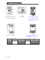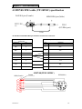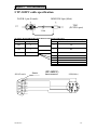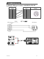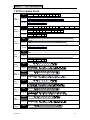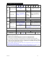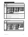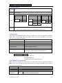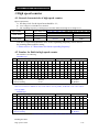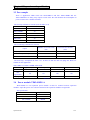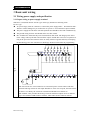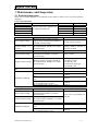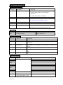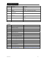
1
TP03 PLC USER Manual TP03 Programmable Logic Control 4KA72X123 Version: 1.6 2011-4-29 0086-0510-8522-7555 Contents Chapter 1 TP03 Introduction......................................................................................................... 1-1 1 Model type description....................................................................................................... 1-2 2 Product type ....................................................................................................................... 1-3 2.1 Basic module list ..................................................................................................... 1-3 2.2 Expansion module list ............................................................................................. 1-6 2.3 Programming tool.................................................................................................... 1-9 2.4 Accessory list ........................................................................................................ 1-10 3 System configuration ........................................................................................................1-11 4 OP07/08-TP03 cable (TP03-302MC) specification ......................................................... 1-12 5 TP03-302PC cable specification ...................................................................................... 1-13 6 TP03 PC/PDA port connect with HMI by RS-422........................................................... 1-14 7 TP03 terminal block......................................................................................................... 1-15 Chapter 2 Basic Unit Specification ............................................................................................. 2-1 1 Function ............................................................................................................................. 2-1 1.1 General specification............................................................................................... 2-1 1.2 AC type Power supply specification ....................................................................... 2-4 1.3 DC type Power supply specification ....................................................................... 2-4 1.4 General features for basic unit ................................................................................ 2-5 1.5 Environment specification....................................................................................... 2-6 2 Digital input/output ............................................................................................................ 2-7 2.1 Digital input ............................................................................................................ 2-7 2.2 Digital output point ................................................................................................. 2-7 3 Communication ports ....................................................................................................... 2-10 3.1 Communication ports position .............................................................................. 2-10 3.2 Three communication ports description ................................................................ 2-13 3.2.1 Modbus slave communication.................................................................... 2-13 3.2.2 Data link ..................................................................................................... 2-21 3.2.3 REMOTE I/O instruction ........................................................................... 2-21 3.2.4 RS/MBUS instruction ................................................................................ 2-22 3.3 Wiring methods..................................................................................................... 2-23 4 High speed counter........................................................................................................... 2-25 4.1 General characteristic of high speed counter ........................................................ 2-25 4.2 Number for Built-in high speed counter................................................................ 2-25 4.3 Function ................................................................................................................ 2-27 4.4 Application example for 1 phase high speed counter............................................ 2-27 4.4.1 1 Phase 1 input ........................................................................................... 2-27 4.4.2 1 Phase 2 input ........................................................................................... 2-28 4.5 Application example for 2 phase high speed counter............................................ 2-29 4.5.1 2 Phase 2 inputs.......................................................................................... 2-29 4.5.2 Action of 2 phase input signal .................................................................... 2-29 4.6 Output counting result........................................................................................... 2-30 4.7 Restrictions for fastest responding frequency ....................................................... 2-30 4.8 Common consideration: ........................................................................................ 2-31 5 Interruption Input ............................................................................................................. 2-32 6 Pulse output...................................................................................................................... 2-33 7 Expansion card................................................................................................................. 2-33 8 Built-in memory and memory card (TP03-1ME)............................................................. 2-34 9 Password .......................................................................................................................... 2-35 10 RUN/STOP switch ......................................................................................................... 2-35 11 RTC ................................................................................................................................ 2-36 12 Potentiometer ................................................................................................................. 2-37 13 Battery............................................................................................................................ 2-38 14 Instruction ...................................................................................................................... 2-38 I Chapter 3 Expansion unit specification....................................................................................... 3-1 1 Digital expansion unit ........................................................................................................ 3-1 1.1 General specification............................................................................................... 3-1 1.2 Outline dimension ................................................................................................... 3-2 1.2.1 TP02 digital expansion unit.......................................................................... 3-2 1.2.2 TP03 digital expansion unit.......................................................................... 3-2 1.3 Electric specification............................................................................................... 3-3 1.3.1 TP02-16EXD Specification.......................................................................... 3-3 1.3.2 TP02-16EYR Specification.......................................................................... 3-4 1.3.3 TP02-16EYT specification........................................................................... 3-5 1.3.4 TP02-16EMR Specification ......................................................................... 3-6 1.3.5 TP02-32EMR Specification ......................................................................... 3-7 1.3.6 TP03-16EMR Specification ......................................................................... 3-8 1.3.7 TP03-16EMT Specification ......................................................................... 3-9 1.3.8 TP03-16EMT P Specification ................................................................. 3-10 1.3.9 TP03-16EYR Specification.........................................................................3-11 1.3.10 TP03-16EYT Specification ...................................................................... 3-12 1.3.11 TP03-16EYT P Specification ................................................................ 3-13 1.3.12 TP03-16EXD Specification...................................................................... 3-14 2 Analogue expansion unit .................................................................................................. 3-15 2.1 Introduction ........................................................................................................... 3-15 2.1.1 Brief ........................................................................................................... 3-15 2.1.2 Data register and channel of analog expansion module. ............................ 3-16 2.1.3 Setting the system memory ........................................................................ 3-17 2.2 General Specification for analog expansion unit .................................................. 3-19 2.3 Dimension ............................................................................................................. 3-19 2.3.1 TP02 analog expansion unit ....................................................................... 3-19 2.3.2 TP03 analog expansion unit ....................................................................... 3-19 2.4 Wiring for analog expansion module .................................................................... 3-20 2.5 Electric Specification ............................................................................................ 3-22 2.5.1 TP02-4AD+ Specification.......................................................................... 3-22 2.5.2 TP03-8AD Specification ............................................................................ 3-23 2.5.3 TP03-4RD Specification ............................................................................ 3-24 2.5.4 TP03-4RD-K Specification………………………………………………..3-25 2.5.5 TP03-4TM Specification............................................................................ 3-26 2.5.6 TP02-2DA+ Specification.......................................................................... 3-27 2.5.7 TP03-2DA Specification ............................................................................ 3-28 2.5.8 TP03-3MA Specification............................................................................ 3-29 3 How many expansion unit can be connected to base unit ................................................ 3-31 3.1 Specification.......................................................................................................... 3-31 3.2 Power consumption............................................................................................... 3-31 3.2.1 5V power provide by base unit................................................................... 3-31 3.2.2 5V power consumed by expansion unit...................................................... 3-31 3.2.3 24V internal power provide by base unit ................................................... 3-31 3.3 For example........................................................................................................... 3-32 3.4 Power module TP03-01SPS-A.............................................................................. 3-32 Chapter4 Dimension and installation .......................................................................................... 4-1 1 Outline dimension .............................................................................................................. 4-1 1.1 Basic unit................................................................................................................. 4-1 1.2 TP02 expansion unit................................................................................................ 4-2 1.3 TP03 expansion unit and power unit....................................................................... 4-3 1.4 TP03 communication unit ....................................................................................... 4-3 2 Installation.......................................................................................................................... 4-5 2.1 Ambient environment.............................................................................................. 4-5 2.2 Installation of basic unit and expansion unit ........................................................... 4-5 2.2.1 Directly installation ...................................................................................... 4-6 2.2.2 DIN Rail installation .................................................................................... 4-8 2.3 Installation for expansion cable and termination connector.................................... 4-8 II Chapter 5 Wiring......................................................................................................................... 5-1 1 Wiring ................................................................................................................................ 5-1 2 Basic unit wiring ................................................................................................................ 5-2 2.1 Wiring power supply and specification................................................................... 5-2 2.1.1 Input wiring at power supply terminal ......................................................... 5-2 2.1.2 Protection circuit: ......................................................................................... 5-3 2.2 Input wiring............................................................................................................. 5-4 2.3 Output wiring .......................................................................................................... 5-5 3 Expansion unit wiring ........................................................................................................ 5-7 3.1 Input wiring for expansion unit............................................................................... 5-7 3.2 Output wiring for expansion unit ............................................................................ 5-8 4 Wiring consideration .......................................................................................................... 5-9 4.1 Wiring consideration for Input power terminal....................................................... 5-9 4.1.1 When Built in DC24V power supply share Common terminal with External power..................................................................................................................... 5-9 4.2 Wiring consideration for Input terminal:................................................................. 5-9 4.2.1 Wiring consideration for different Input devices (sensor/ switch…) ......... 5-10 4.2.2 Leakage current of Input component...........................................................5-11 4.3 Output terminal wiring consideration: .................................................................. 5-12 4.3.1 Surge current from Indicator load: ............................................................. 5-12 4.3.2 Surge voltage of inductive load.................................................................. 5-12 4.3.3 Driving a light load .................................................................................... 5-13 4.3.4 Lifespan of relay ........................................................................................ 5-13 4.3.5 Wiring consideration for TP03 HT type PLC ....................................... 5-13 4.3.6 Wiring consideration for TP03 HT P type PLC.......................................... 5-13 5 Solving noise problem...................................................................................................... 5-14 5.1 Power source noise................................................................................................ 5-14 5.2 Solving thunder stroke problem ............................................................................ 5-15 5.3 Anti-Noise for Expansion Cable ........................................................................... 5-16 5.4 Anti-Noise for I/O Wiring..................................................................................... 5-16 Chapter 6 Trial Run..................................................................................................................... 6-1 1 Trial run.............................................................................................................................. 6-1 1.1 Safety ...................................................................................................................... 6-1 1.2 Before Trial run....................................................................................................... 6-1 1.3 Trial run step ........................................................................................................... 6-2 2 Maintenance and Inspection............................................................................................... 6-3 2.1 Periodical inspection ............................................................................................... 6-3 2.1.1 General items: .............................................................................................. 6-3 2.1.2 Basic unit:..................................................................................................... 6-3 2.1.3 Expansion units: ........................................................................................... 6-3 3 Troubleshooting ................................................................................................................. 6-4 3.1 LED indicator status................................................................................................ 6-4 3.2 Presumption of troubleshooting procedure ............................................................. 6-4 3.3 Preparation for troubleshooting............................................................................... 6-4 3.4 Check the following again....................................................................................... 6-5 3.5 Troubleshooting procedure ..................................................................................... 6-6 3.5.1 Troubleshooting procedure - 1 ..................................................................... 6-6 3.5.2 Troubleshooting procedure - 2 ..................................................................... 6-7 3.5.3 Troubleshooting procedure - 3 ..................................................................... 6-8 3.5.4 Troubleshooting procedure - 4 ..................................................................... 6-8 3.5.5 Troubleshooting procedure - 5 ..................................................................... 6-9 Chapter 7 Instruction List ........................................................................................................... 7-1 1 Basic sequential instruction................................................................................................ 7-1 2 Step instruction :STL, RET................................................................................................ 7-3 3 Application instruction list ................................................................................................. 7-4 III Chapter 8 Special Relay.............................................................................................................. 8-1 PC status (M) ........................................................................................................................ 8-1 Clock device (M) .................................................................................................................. 8-1 Operation flags (M)............................................................................................................... 8-1 PC status (D) ......................................................................................................................... 8-2 RTC (D)................................................................................................................................. 8-2 PC operation mode (M)......................................................................................................... 8-3 PC mode (D) ......................................................................................................................... 8-3 Step ladder flags (M)............................................................................................................. 8-3 Step ladder flags (D) ............................................................................................................. 8-3 Interruption disable (M) ........................................................................................................ 8-4 UP/DOWN counting set device (M) ..................................................................................... 8-4 Devices (M)........................................................................................................................... 8-6 Error detection (D) ................................................................................................................ 8-6 Communication and link (M) I ............................................................................................. 8-6 Communication and link (D) I .............................................................................................. 8-8 Communication and link (M) II .......................................................................................... 8-10 Communication and link (D) II............................................................................................8-11 High speed and position (M)............................................................................................... 8-12 Expansion (M)..................................................................................................................... 8-12 Expansion function (D)....................................................................................................... 8-13 High speed and position (D) ............................................................................................... 8-13 PWM output (D) ................................................................................................................. 8-13 OP07/08 (M) ....................................................................................................................... 8-14 OP07/08 (D)........................................................................................................................ 8-15 AD/DA (M)......................................................................................................................... 8-16 AD/DA (D).......................................................................................................................... 8-16 IV Chapter 1 TP03 Introduction Chapter 1 TP03 Introduction...................................................................................... 1-1 1 Model type description .................................................................................... 1-2 2 Product type ..................................................................................................... 1-3 2.1 Basic module list.................................................................................... 1-3 2.2 Expansion module list............................................................................ 1-6 2.3 Programming tool .................................................................................. 1-9 2.4 Accessory list ....................................................................................... 1-10 3 System configuration ......................................................................................1-11 4 OP07/08-TP03 cable (TP-302MC) specification........................................... 1-12 5 TP-302PC cable specification........................................................................ 1-13 6 TP03 PC/PDA port connect with HMI by RS-422 ........................................ 1-14 7 TP03 terminal block....................................................................................... 1-15 Introduction 1-0 Chapter 1 TP03 Introduction Chapter 1 TP03 Introduction TP03 is the latest generation of PLC developed by TECO. The high-speed and high-quality programmable logic controller has following features: High speed of executive time. Basic instructions: 0.31us / step (ANDB), 0.45us/step (LD) Large memory capacity: Program memory capacity: 4~8~16k steps. The product has integrated basic and application instructions, such as operation instructions, ADD/SUB/MUL/DIV…etc. trigonometry instructions as SIN /COS /TAN…, matrix input, and other instructions as matrix input, 7-seg output, and PID. Flexible expansion ability Basic units: 14/20/26/30/36/40/60 point types, max can expand to 256 digital points. 60/10 (12 bits) analog input /output 3 communication ports, and with 3 functions (please refer to Chapter 3: communication port for detailed information) are available for Basic unit. Using any one of them can establish a network.. PC/PDA port is also for download/upload the program to/from TP03. Computer link: ONE computer can control as many as 255 TP03s. Data link: When a TP03 is set as master, it can control other 15 TP03s. Each PLC can receive max (64 bits+8 words) ×15 data. Remote I/O: TP03 is set as master; it can control as much as 4 other TP03s. Each slaver has MAX input 36 points; output 24 points: Compliant with Modbus: Modbus protocol has embeded in TP03. It’s easy to comminucation with inverter or HMI. Built-in RTC, PWM, RUN/STOP switch, two VR (potentiometers), flash memory, and the product is available for expansion modules, A/D, D/A module and etc. Built-in high speed 100K pulse output which can control servo controller. High speed counter: With max speed 100K single phase, the counter has the function of two/single phase high speed and interruption input which enable precisely controlling the pulse input signal from encoder. TP03 series products have the same height: 90mm. TP03 is very easy to operate for those who have used Mitsubishi FX series. Profibus-DP, DeviceNet, EtherNet (TCP/IP) communication module is optional Easy to maintain and installation, as terminal block is pluggable (only 40/60 points type), Din rail installation PDA edits software (programming language: instruction list, IL) TP02 expansion modules are available for TP03 The three programming languages, LD (Ladder Diagram, IL(Instruction List) and SFC Introduction 1-1 Chapter 1 TP03 Introduction (Sequential Function Chart) are all available for TP03. The system program can be updated directly by the controller 1 Model type description Main Module Type No. description TP03 - 20 H T - A P Transistor type: “P” PNP transistor No “P” (blank) NPN transistor Power supply: A:AC 100V~240V D: DC 20.4V~28.8V Output R:Relay T: transistor Function M:Standard H:Advanced S:Simple Point 14:14 point 20:20 point 26:26 point 30:30 point 36:36 point 40:40 point 60:60 point Product Series Expansion module Type No. description TP03 - 16 E M T P Transistor type: “P”: PNP transistor No “P” (blank): NPN transistor Input/Output type D: 24VDC Input (Module type is X only) R: Relay Outpu T: transistor Module type M: 24VDC input point and output point share half X: all points are 24VDC input Y: all points are for output E:Expansion module Point 16:16 point 32:32 point Product series TP03-01SPS-A : Power expansion module Introduction 1-2 Chapter 1 TP03 Introduction Analog expansion module Type No. description TP03 - 8 AD Analog module type AD: analog input RD: PT-100 temperature input RD-K: PT-1000 temperature input TM: J/K temperature input DA: analog output MA: analog input and output Channel 2: 2channels 4: 4 channels 8: 8 channels 3: Output: 1 channel;Input: 2 channel (MA available) Product series 2 Product type 2.1 Basic module list Type Input point User’s Rated 24vDC Input current battery point type current point TP03-14SR-A TP03-20SR-A 250mA TP03-26SR-A TP03-36SR-A TP03-20MR-A 100~240 VAC TP03-30MR-A 300mA TP03-20HR-A TP03-30HR-A TP03-40HR-A 500mA TP03-60HR-A TP03-40HR-D 21.6~28.8 N.A TP03-60HR-D VDC TP03-30MR-D TP03-20MT-A TP03-30MT-A 300mA TP03-20HT-A TP03-30HT-A TP03-40HT-A 500mA TP03-60HT-A 100~240 TP03-20MT-A P VAC TP03-30MT-A P TP03-20HT-A P 300mA TP03-30HT-A P TP03-40HT-A P TP03-60HT-A P Introduction 8 12 16 20 12 16 12 16 24 36 24 36 16 24VDC 7mA 12 16 12 16 24 36 12 16 12 16 24 36 Output point Max output type point dimension 6 116×92×64mm Fig 3 8 10 177×92×64mm Fig 4 16 8 116×90×83mm 14 2A/ point Relay Fig 1 8 (5A/COM) 14 16 24 177×90×83mm Fig 2 16 24 14 8 116×90×83mm 14 Fig 1 8 14 14 177×90×83mm Fig 2 24 0.3A/ point transistor (1.2A/COM) 8 14 8 116×90×83mm Fig 1 14 16 24 1-3 Chapter 1 TP03 Introduction Profile referring figure: Fig 1 Fig 2 Fig 3 Fig 4 Nameplate description Software version Software version TP03 model Power specification Model : TP03-60HR-A VX.X Power : 100~240VAC 50/60Hz 50VAmax. Input specification Input : 24VDC/7mA Output specification Output : 250VAC/2A; DC30V/2A Auxiliary power output AUX. Output: 24VDC/500mAmax. Introduction C TP03 model Power specification Model : TP03-60HR-A VX.X C Power : 100~240VAC 50/60Hz 50VAmax. C US LISTED 85FM Input specification Input : 24VDC/7mA IND. CONT. EQ. E205406 Output specification Output : 250VAC/2A; DC30V/2A Auxiliary power output AUX. Output: 24VDC/500mAmax. R 1-4 Chapter 1 TP03 Introduction Series number/Bar Code description (21) Y WW A BCD XXX 28 01020304 Hardware version (01~99) Software version(01~99) Manufacture s/n(000~999) Product code (000~999) Producing plant code(0) Producing Week (01~53) Producing year (0~9) Fixed code (21) Product profile and components introduction 1. Power supply terminals 2. RS485 port 3. Run/stop switch 4. 2 groups of potentiometer 5. PC/PDA communication port 6. Expansion port 7. Battery 8. Memory pack port 9. Input terminal block 10. Running indicator 11. Input and output indicator 12. Expansion connector 13. Product label 14. Series number 15. DIN rail groove 16. retractable installation hole 17. Output terminal block Introduction 1-5 Chapter 1 TP03 Introduction 2.2 Expansion module list Peripheral equipment Power Type No. Description Source OP07 N.A 2 line LCD, timer and counter setting device OP08 24Vdc 2 line LCD, timer and counter setting device Profile referring figure: OP07/OP08 Remark Fig 5 Fig 5 Fig 5 Expansion card Type No. TP03-0CV Built-in TP03-6AV TP03-2TI Optional TP03-485RS TP03-2AI TP03-1ME Profile referring figure: description Standard cover Analog potentiometer input port*6 Timer input port*2 RS485 multi-function communication port 0~10V analog input port *2(10 bit) Memory pack Remark (Fig 6) In developing (Fig 7) In developing (Fig 8) (Fig 9) In developing (Fig 10) (Fig 11) TP03-0CV (Fig 6) TP03-6AV (Fig 7) TP03-2TI (Fig 8) TP03-485RS (Fig 9) TP03-2AI (Fig 10) TP03-1ME (Fig 11) Note: If you want to read the data of TP03-2AI/TP03-2TI, you need to use the applied instruction F89 EPSC; if you want to read the data of TP03-6AV, you need to use the applied instruction F85 VRRD or F86 VRSC. See more details in <TP03 Programming manual>, Chapter 6 Applied Instruction Interpretation. Introduction 1-6 Chapter 1 TP03 Introduction Expansion module Power Type No. Source TP02-16EXD TP02-16EYR TP02-16EYT N.A TP02-16EMR TP02-32EMR TP02-4AD+ TP02-2DA+ TP03-01SPS-A TP03-4RD TP03-4RD-K TP03-4TM TP03-2DA TP03-3MA TP03-8AD TP03-16EMR TP03-16EMT TP03-16EMT P TP03-16EXD TP03-16EYR TP03-16EYT TP03-16EYT P Introduction In/out Description point 16 / 0 16 points DC input 0 / 16 16 points relay output 0 / 16 16 points transistor output 8 points DC input & 8 points relay 8/8 output 16 points DC input & 16 points 16 / 16 relay output 0~10V,0~20mA analog input *4 4/0 Channel 24Vdc 0~10V,+/-10V,0~20mA,4~20mA 0/2 analog output *2 channel 100~2 Power source for Expansion N.A 40V modules AC 4 / 0 PT100 temperature input *4 channel 4 / 0 PT1000 temperature input *4 channel 4 / 0 J/K temperature input *4 channel 0~10V,+/-10V,0~20mA,4~20mA 0/2 analog output *2 channel 24V 0~10V,0~20mA analog input *2 DC Channel 2/1 0~10V,+/-10V,0~20mA,4~20mA analog output *1 channel 0~10V,0~20mA analog input *8 8/0 Channel 8 points DC input/ 8 points relay N.A 8/8 output module 8 points DC input/ 8 points NPN N.A 8/8 transistor output module 8 points DC input/ 8 points PNP N.A 8/8 transistor output module 8 points DC input/ 8 points relay N.A 16 / 0 output module N.A 0/16 16 points relay output module 16 points NPN transistor output N.A 0 / 16 module 16 points PNP transistor output N.A 0 / 16 module dimension 64 x 90 x 76 mm 110 x 90 x 76 mm 64 x 90 x 76 mm Remark These modules are all available for both TP02 and TP03. (Fig 12) (Fig 13) (Fig 15) Fig 16 Fig 16 Fig 16 Fig 16 Fig 16 Fig 16 57 x 90 x 83 mm Fig 16 Fig 14 1-7 Chapter 1 TP03 Introduction Profile referring figure: 1 COMA 3 5 7 COMA COMA COMA 2 4 6 8 1 3 2 COMA COMA 5 4 7 6 9 11 13 15 0 COMA 8 10 12 14 16 2 1 COMA 4 3 6 5 7 PWR OE 3 1 3 1 2 6 COM C 4 7 8 5 2 COMc 4 5 6 8 7 COMb 9 11 COMd 0 1 2 4 5 6 3 7 IN 0 1 2 3 OUT 4 5 6 7 14 16 10 12 13 15 COMe COMC 1 3 4 6 CO MD 0 Fig 12 2 Fig 13 TP02-16EXD/ TP02-16EYR/ TP02-32EMR TP02-16EYT/ TP02-16EMR COMD 5 7 Fig 14 TP03-16EMR/ TP03-16EYR/ TP03-16EXD/TP03-16EMT/ TP03-16EMT P/TP03-16EYT/ TP03-16EYT P +24V V1 C1 V2 C2 + 2 4 V TC 0 + TC0 - TC1 + TC1 - 0V 11 SHLD 12 SHLD 0V PWR LNK Power V1 C3 SHLD V2 C4 TC2 + TC2 - TC3 + TC3 - SHLD Fig 15 TP02-4AD+/ TP02-2DA+ Fig 16 TP03-4RD/TP03-4RD-K/TP03-4TM/ TP03-2DA/TP03-3MA/TP03-8AD/ TP03-01SPS-A Communication module External Input Type No. power TP03-DNET TP03-PBUS 24Vdc EN01 GSM Introduction Description DeviceNet slaver Profibus-DP slaver TCP/IP GSM Dimension 38 x 90 x 59 mm Remark In developing (Fig 17) In developing (Fig 18) In developing (Fig 19) In developing (Fig 20) 1-8 Chapter 1 TP03 Introduction Profile referring figure: TP03-DNET (Fig 17) TP03-PBUS (Fig 18) MS NS GS EN01 (Fig 19) M GSM (Fig 20) 2.3 Programming tool Type No. TP03-PC TP03-PDA Description TP03 PLC PC software (Fig 21) TP03 PLC PDA software Remark The type no. for CD is TP03-CD06 (Fig 20) X000 CALL P1 OUT Y001 X001 FEND X002 OUT Y002 SRET TP03-CD06 Disk (Fig 20) Introduction TP03-PC Disk (Fig 21) 1-9 Chapter 1 TP03 Introduction 2.4 Accessory list Built-in accessory Basic module Built-in description Terminal connector (Fig 22) Battery ( for 5years) RS-485 built-in (H type only) Standard cover for Expansion card Type No. TP-200EC TP03-0CV Installation manual TP02 expansion Built-in module Option Built-in TP03 expansion module Option Built-in PC06 4cm cable for expansion module (Fig 23) 40cm cable for expansion module (Fig 23) 4cm cable for expansion module (Fig 24) 40cm cable for expansion module (Fig 24) 1.8M cable(black) (Fig 25) Compact Disk TP-042EC TP-402EC TP03-304EC TP03-340EC 26 pins, Only for TP03 expansion module TP03-302PC Include: TP03-PC TP03-PDA PDF files of instruction manual & operation manual TP03-CD06 Option PDA adapter (Fig 26) Built-in 1.8M cable (grey) (Fig 25) OP07/OP08 Option 5M cable (grey) (Fig 25) Profile referring figure: Remark Install TP-200EC into the connector in the last expansion module in order to form a I/O loop,if no expansion module must install into the TP03 host 14 pins, Only for TP02 expansion module JNSWPDA TP03-302MC TP03-305MC Only for OP08 Fig 22 Fig 23 Fig 24 TP-200EC TP-042EC(4cm)/ TP-402EC(40cm) TP03-304EC(4cm)/TP03-340EC(40cm) Fig 25 TP03-302PC(black) / TP03-302MC(grey) Fig 26 (both items are different in outline, color and internal wiring) PDA Adapter (JNSWPDA) TP03-305MC(grey) (same outline and color as TP03-302MC, but different in length and internal wiring) Introduction 1-10 Chapter 1 TP03 Introduction 3 System configuration Basic module TP03-40/60 TP02 expansion module Expansion cable TP-042EC (4cm) TP-402EC(40cm) TP02-16EXD/TP02-16EYR/ TP02-16EYT/TP02-16EMR/ TP02-4AD+/TP02-2DA+ Terminal connector TP02-32EMR TP-200EC TP03-20/30 Expansion cable TP03 expansion module TP03-304EC (4cm) TP03-4TM / TP03-4RD/ TP03-4RD-K/ TP03-2DA / TP03-340EC(40cm) TP03-3MA / TP03-8AD/ TP03-01SPS-A Terminal connector TP03-16EMR/TP03-16EYR/ TP-200EC TP03-16EXD/TP03-16EMT/ TP03-16EMT P/TP03-16EYT/ TP03-16EYT P +24V V1 0V V3 V6 C5 V7 3 1 7 6 4 P WR IN C8 5 2 COMA V8 C7 C6 1 COMA C4 RU N V5 SHLD V4 C3 C2 PWR 8 RU N 2 3 4 5 6 7 8 1 2 3 4 5 6 7 8 OU T 3 1 2 PC/PDA cable (TP03-302PC) V2 C1 6 COMC 4 5 IN OU T 7 8 COMD OP07/08 cable (TP03-302MC/TP03-305MC) OP07/08 PDA adapter (JNSWPDA ) PC 5 9 7 8 9 2 6 0 4 5 6 3 7 1 1 2 3 4 8 2 MOD1 MOD2 0 EST TMR CNT ENT PDA Introduction 1-11 Chapter 1 TP03 Introduction 4 OP07/08-TP03 cable (TP-302MC) specification D-SUB 9 pin (Female) MINI DIN 8pin (Male) OP07/08 侧 TP03 (PC/PDA port) 1.8m TP-302MC D-SUB/MINI DIN pin definition and internal connection: D-SUB 9pin(Female) (OP07/08) definition pin N.C 1 MINI DIN 8pin(Male)(TP03 PG (PC/PDA) port) pin definition TX+ 2 2 RX + RX+ 3 7 TX + N.C 4 6 GND GND 5 3 GND N.C 9 8 GND Vcc 6 5 Vcc TX- 7 1 RX - RX- 8 4 TX - OP07/08(TP03-302MC) 9PIN(Female) 5 9 4 8 3 7 2 6 1 Introduction Shield 8PIN(Male) 7 6 3 8 4 1 5 2 1-12 Chapter 1 TP03 Introduction 5 TP-302PC cable specification MINI DIN 8pin (Male) D-SUB 9 pin (Female) TP03 (PC/PDA port) PC 1.8m TP-302PC D-SUB/MINI DIN pin definition and internal connection: D-SUB 9pin(Female) MINI DIN 8pin(Male)(TP03 PG (PC/PDA) port) definition pin pin definition RX 2 4 TX - TX 3 1 RX - GND 5 3 GND 6 8 5 7 2 GND GND Vcc TX + RX + 9PIN(Female) 5 9 4 8 3 7 2 6 1 Introduction Shield (TP-302PC) 4KA97X249W22 8PIN(Male) 7 6 3 8 4 1 5 2 1-13 Chapter 1 TP03 Introduction 6 TP03 PC/PDA port connect with HMI by RS-422 Take OP10 HMI as an example 0P10 COM1 1 TX+ 2 RX 3 TX 4 NC 5 GND 6 TX7 VCC 8 RX9 RX+ Shield 9PIN(Female) TP03 PC/PDA Port RX1 RX+ 2 GND 3 TX4 VCC 5 GND 6 TX+ 7 GND 8 (TP03-102MC ) 8PIN(Male) 5 9 4 8 3 7 2 6 1 CO M CO M 0 1 2 3 5 4 TP03 PC/PDA port (Female) 7 6 4 3 1 7 6 10 11 12 8 5 2 13 RU N P WR +24V RU N S TOP o ut put 0V SR-A Series IN SG 0 1 2 3 4 5 6 7 0 1 2 3 4 5 6 7 10 12 11 13 OUT B A 2 0 S R-A COM 0 0 1 2 3 CO M1 4 5 6 7 TP03-102MC TP03 Series Introduction 1-14 Chapter 1 TP03 Introduction 7 TP03 terminal block TP0314SR-A Input COM Output COM0 Comm TP0320SR-A TP0326SR-A TP0336SR-A TP0320MR-A TP0330MR-A TP0320HR-A TP0330HR-A TP0320MT-A TP0330MT-A Introduction 0 COM 0 +24V 1 COMA COMA Output COMB 0 Comm +24V 0V Input COM COM 0 Output COM0 0 Input COM COM 0 COM0 0 Comm +24V Input 1 3 2 3 SG 0 5 4 5 2 A B SG A B SG 0 0V COM 13 14 15 16 17 0 2 1 4 15 10 7 11 10 12 COM3 14 13 15 12 11 13 5 6 5 7 6 COM2 3 4 3 10 7 2 14 13 7 COM2 5 6 COM1 12 COM3 6 4 5 1 0 + 2 4 V COM 12 12 14 16 11 13 15 17 3 4 3 COM0 N 10 7 2 11 10 COM2 5 6 CO M1 2 6 4 5 1 100~240VAC L 11 12 11 13 3 1 CO M0 CO M 10 4 7 COM2 7 2 0 0V 7 13 6 5 6 3 N + 2 4 V COM 4 5 2 1 100~240VAC L 6 12 10 12 14 16 11 13 15 17 3 COM1 0 CO M 5 11 7 COM2 5 7 2 1 0 0V 4 6 4 COM0 + 2 4 V CO M 10 10 1 2 11 13 5 3 N 7 10 11 12 13 14 15 16 17 20 21 22 23 3 4 2 100~240VAC L 7 CO M1 1 6 7 COM1 1 0 2 1 0 COM 6 3 0 0V 7 7 COM1 10 11 6 7 6 COM1 CO M0 + 2 4 V COM 6 1 2 N 6 10 11 12 13 14 15 16 17 7 6 5 5 1 1 0 0 ~ 2 40 V A C L 5 4 3 0 COM 4 5 A 0 0V 5 7 A COM0 + 24V COM 4 4 4 1 COM 3 4 B N Input Output 2 4 6 A B 1 0 0~ 24 0 V A C L Input Output 1 5 COMC 3 SG 0V Input Output 2 + 2 4V COM Input Output 2 3 2 0V Input 1 B 1 0V Output A 3 SG 4 COM1 B 2 1 +24V Output 0 1 3 3 SG Input 2 2 0V Comm 1 7 6 12 14 16 17 11 13 15 1-15 Chapter 1 TP03 Introduction 100~240VAC L 0 N Input TP0320HT-A 0 + 2 4 V COM 2 B SG 4 1 COM0 7 2 0 N 10 5 6 11 10 14 12 13 COM3 15 12 11 13 4 7 COM2 3 CO M1 7 COM2 5 6 3 100~240VAC L 4 3 COM1 1 CO M 0V A Output 2 1 CO M 0 Output 5 6 Note: COM0 of HT type is connected with user 0V internally TP0330HT-A 0 + 24V COM Input 0V A Output B SG 6 5 2 0 N 4 3 1 COM0 1 00 ~2 40V A C L 2 1 COM 4 7 COM2 3 COM1 10 12 14 16 11 13 15 17 7 5 11 10 6 12 14 13 CO M3 15 Note: COM0 of HT type is connected with user 0V internally TP0340HR-A Output 0 + 2 4 V COM Input 0V A B SG 0 TP0340HR-D TP0360HR-D TP0330MR-D A SG A + 24VDC 2 B SG 0 2 1 COM A B SG 24VDC + 1 CO M0 4 3 0V 0V A 0 2 B SG 3 7 2 21 17 COM4 15 16 20 22 COM5 24 23 26 25 27 1 4 CO M4 1 7 13 15 16 10 7 2 1 4 COM4 1 7 21 22 24 26 1 3 1 5 1 6 2 0 CO M5 2 3 2 5 2 7 4 7 COM2 5 11 10 6 12 14 13 COM3 15 12 14 16 20 22 24 26 11 13 15 17 21 23 25 27 4 7 COM2 3 CO M1 12 COM3 10 12 14 16 11 13 15 17 3 CO M1 6 0 12 COM3 11 10 6 5 1 1 COM0 N 11 10 7 6 4 3 5 6 COM2 5 2 1 4 1 100~240VAC L 4 0 COM 7 CO M2 5 3 CO M0 + 2 4 V COM 14 13 12 14 16 20 22 24 26 30 32 34 36 40 42 11 13 15 17 21 23 25 27 31 33 35 37 41 43 10 0 N 12 COM3 6 2 1 0 0 ~ 2 40 V A C L 4 7 COM 10 3 CO M1 + 24V COM Input 11 7 6 12 14 16 20 22 24 26 11 13 15 17 21 23 25 27 2 1 0 COM 3 COM1 5 COM0 - 10 COM2 5 7 0 0V 4 3 10 5 1 2 1 4 COM 4 1 7 13 15 16 11 6 12 14 16 20 22 24 26 30 32 34 36 40 42 11 13 15 17 21 23 25 27 31 33 35 37 41 43 2 6 3 7 COM 2 5 10 CO M1 4 1 - + 2 4 V COM Input Output 0 CO M 4 7 1 COM0 12 14 16 20 22 24 26 11 13 15 17 21 23 25 27 3 6 5 0 COM Output Output 4 N Input TP0340HT-A B 2 CO M1 3 1 0 0 ~2 4 0 V AC Input Output 2 1 COM 10 7 1 COM 0 0 0V L 6 5 N Input Output 4 3 100~240VAC L + 2 4 V COM TP0360HR-A 2 1 COM 5 6 12 11 10 14 13 COM3 CO M 4 15 17 16 Note: COM0 of HT type is connected with user 0V internally Input TP0360HT-A Output + 2 4 V COM 0V A 0 2 1 COM 4 B SG 5 0 N 7 12 14 16 20 22 24 26 30 32 34 36 40 42 31 33 35 37 41 43 11 13 15 17 21 23 25 27 2 1 COM0 100~240VAC L 10 6 3 4 7 COM2 5 3 COM1 1 2 1 4 CO M4 1 7 2 1 2 2 2 4 2 6 1 3 1 5 1 6 2 0 COM5 2 3 2 5 2 7 11 10 6 COM3 Note: COM0 of HT type is connected with user 0V internally 0 + 2 4 V COM TP03-20 MT-A P TP03-30 MT-A P Introduction Input Output Input 0V 2 + 2 4 V COM 0V COM 5 1 0 N 0 7 2 COM1 2 1 4 5 6 5 12 11 13 COM2 3 4 3 10 6 3 COM0 100~240VAC L 4 1 COM 10 7 7 6 12 14 16 17 11 13 15 1-16 Chapter 1 TP03 Introduction 1 COM0 Output 100~240VAC L Output 0V 0 10 7 11 10 12 COM3 14 13 15 12 11 13 7 COM2 5 6 5 6 6 0V 0 B 0 SG 4 6 3 1 CO M0 A 2 1 COM 2 5 4 10 12 14 16 11 13 15 17 7 COM2 3 COM1 7 5 11 10 6 12 CO M3 14 13 15 Note: the 0V of the high-speed output load must be connected with the user’s 0V of main module. COM0 needs to be connected with the positive of the power of the load. Y0,Y1 need to be connected with the 0V of the power of the load. Output + 2 4 V COM 0 COM 0V 2 4 1 3 1 CO M 0 A B 0 SG 6 5 10 7 2 4 3 COM1 12 14 16 20 22 24 26 11 13 15 17 21 23 25 27 COM2 5 11 7 6 10 12 CO M 3 14 13 COM4 15 17 16 Note: the 0V of the high-speed output load must be connected with the user’s 0V of main module. COM0 needs to be connected with the positive of the power of the load. Y0,Y1 need to be connected with the 0V of the power of the load. Output Note: The ‘ chapter. Introduction 4 3 + 24 V COM Output Input TP03-60 HT-A P 4 3 7 COM2 5 Note: the 0V of the high-speed output load must be connected with the user’s 0V of main module. COM0 needs to be connected with the positive of the power of the load. Y0,Y1 need to be connected with the 0V of the power of the load. Input TP03-40 HT-A P 2 2 COM1 4 3 CO M 1 1 CO M 1 COM0 A B SG Input TP03-30 HT-A P 0 + 2 4 V COM Input TP03-20 HT-A P 2 0 N + 2 4 V CO M 0V 0 COM 2 1 4 COM0 A B SG 0 10 6 3 5 1 7 2 COM1 4 3 12 14 16 20 22 24 26 30 32 34 36 40 42 31 33 35 37 41 43 11 13 15 17 21 23 25 27 COM2 5 6 7 1 1 1 2 14 COM4 17 2 1 2 2 24 2 6 1 0 COM3 1 3 15 1 6 20 COM5 23 2 5 27 Note: the 0V of the high-speed output load must be connected with the user’s 0V of main module. COM0 needs to be connected with the positive of the power of the load. Y0,Y1 need to be connected with the 0V of the power of the load. ’ terminal in the above table will be represented by ‘FG’ in the following 1-17 Chapter 2 Basic Unit Specification Chapter 2 Basic Unit Specification............................................................................ 2-1 1 Function ............................................................................................................................. 2-1 1.1 General specification............................................................................................... 2-1 1.2 AC type Power supply specification ....................................................................... 2-4 1.3 DC type Power supply specification ....................................................................... 2-4 1.4 General features for basic unit ................................................................................ 2-5 1.5 Environment specification ...................................................................................... 2-6 2 Digital input/output ............................................................................................................ 2-7 2.1 Digital input ............................................................................................................ 2-7 2.2 Digital output point ................................................................................................. 2-7 3 Communication ports....................................................................................................... 2-10 3.1 Communication ports position .............................................................................. 2-10 3.2 Three communication ports description ................................................................ 2-13 3.2.1 Modbus slave communication.................................................................... 2-13 3.2.2 Data link..................................................................................................... 2-21 3.2.3 REMOTE I/O instruction ........................................................................... 2-21 3.2.4 RS/MBUS instruction ................................................................................ 2-22 3.3 Wiring methods ..................................................................................................... 2-23 4 High speed counter........................................................................................................... 2-25 4.1 General characteristic of high speed counter ........................................................ 2-25 4.2 Number for Built-in high speed counter ............................................................... 2-25 4.3 Function ................................................................................................................ 2-27 4.4 Application example for 1 phase high speed counter............................................ 2-27 4.4.1 1 Phase 1 input ........................................................................................... 2-27 4.4.2 1 Phase 2 input ........................................................................................... 2-28 4.5 Application example for 2 phase high speed counter............................................ 2-29 4.5.1 2 Phase 2 inputs.......................................................................................... 2-29 4.5.2 Action of 2 phase input signal .................................................................... 2-29 4.6 Output counting result........................................................................................... 2-30 4.7 Restrictions for fastest responding frequency ....................................................... 2-30 4.8 Common consideration: ........................................................................................ 2-31 5 Interruption Input ............................................................................................................. 2-32 6 Pulse output...................................................................................................................... 2-33 7 Expansion card................................................................................................................. 2-33 8 Built-in memory and memory card (TP03-1ME)............................................................. 2-34 9 Password .......................................................................................................................... 2-35 10 RUN/STOP switch ......................................................................................................... 2-35 11 RTC ................................................................................................................................ 2-36 12 Potentiometer ................................................................................................................. 2-37 13 Battery............................................................................................................................ 2-38 14 Instruction ...................................................................................................................... 2-38 Contents 2-0 Chapter 2 Basic Unit Specification Chapter 2 Basic Unit Specification 1 Function (-14S short for : 14 points, S type,as 14SR-A -20M short for: 20 points, M type, as TP03-20MR-A/TP03-20MT-A etc -40H short for: 40 points, H type, as TP03-40HR-A/TP03-40HT-A/TP03-40HR-D etc.) 1.1 General specification Type Item Basic unit outline Operation control Input/ output Program language Program capacity Retention Digital input Digital I/O Digital output -14S -20S -26S -36S -20M 30M -20H 30H -40H -60H Brick type Reciprocating scan the program in the memory Scanning from Start to End (End instruction) then from Start to End again Ladder /Boolean/SFC (Ladder / IL / SFC) 4K steps 8K steps 16K steps Lithium power supply (with out 5 years lifespan) Flash retain 8 12 16 20 12 16 12 16 24 36 6 8 10 16 8 14 8 14 16 24 Reexpand to Digital module Reexpand to 80 points Reexpand to 256 points ※1 128 points Expansion module + Analog module + 2 xTP02- 4AD & 1 x TP02-2DA Or 1 x TP03-8AD &1 x TP03-2DA ※3 1 x TP02-4AD+ & 1 x TP02- 2DA+ & 7 x TP03-8AD & 4 x TP03-2DA Scan time 60 input channels /10 output channels(at most use 7 input modules, 8 8 input channels /2 output channels (at most use 1 input output channels. module, 2 output channels. See more details in <TP03 Max Analog I/O See more Programming manual>, Chapter 3.2 Analogue expansion details in unit.) <TP03 Programming manual>, Chapter 3.2 Analogue expansion unit.) 36 ANB/ORB …ec ANB/ORB …ect: 0.62μs/ step t: 0.31μs/ step Basic instruction LD/AND/OR… LD/AND/OR…ect: 0.9μs/ step ect: 0.36 --0.45μs/ step Application 126 138 144 instruction Digital I/O relay X000~X377(256 points) / Y000~Y377(256 points) General auxiliary relay: General auxiliary relay: M0~M7679 ( 7680 Auxiliary relay M0~M1535 ( 1536 points) points) Special auxiliary relay: M8000~M8511 ( 512points) Relay and register Function 2-1 Chapter 2 Basic Unit Specification Type Item Step relay Timer Counter Data register Index register Nest pointer -14S -20S -26S -36S -20M 30M -20H 30H -40H -60H S0~S1023 (1024 points) S0~S4095 (4096 points) 512 points .100ms: 200 100 points .100ms: 44 points(T0~T39,T196~T199); points(T0~T199);10ms: 46 points(T200~T245);1ms with accumulating 10ms: 46 function: 4 points(T246~T249);100 ms with points(T200~T245);1ms with accumulating function: accumulating function: 6 points(T250~T255);1ms: 256 4 points(T246~T249);100 ms with accumulating points(T256~T511) . ※5 function: 6 (Refer to Instruction Manual chapter 2 -2.6) points(T250~T255) Analog potentiometer timer: 2 points 136points.16bit:90points(C0 256 points.16 bit: 100 points(C0~C99), 16bit ~C89),16bit with accumulating function: 100points with accumulating function: (C100~C199), 32bit with accumulating 10points(C90~C99),32bit function:35points (C200~C234),32bit 1 phase with accumulating function: 1 input:11points(C235~C245), 36points(C220~C234),32bit1 32bit 1 phase 2 input:4points(C246~C249), phase 1 input: 6points 32bit 2 phase 2 input:4points(C251~C254) (C235~C238,C241~C242), (Refer to Instruction Manual chapter 2 32bit1 phase 2 input: 2points -2.7,2.8) (C246~C247),32bit2 phase 2 input: 3points(C251~C253) General General register:D0000~D7999(8000points); register:D0~D511(512points File register:D2000~D3299 (1300 points) ) Special register:D8000~D8511 (512points) Supplementary register:W0~W 9999(Available N.A. since H/M V2.3) ※4 32points: V000~V0015 / Z000~Z0015 Mark: N0~N7 (8points), pointer P0~P127 (128 Mark: N0~N7 ( 8points), pointer P0~P255 points), input interruption (256 points), input interruption pointer: pointer: I00~I30 (4points), I00~I50 (6points), timer interruption pointer: timer interruption pointer: I6**~I8** (3points), counter interruption I6**~I8** (3points), counter pointer I010~I060 (6points) interruption pointer I010~I060 (6points) 16 Bit : -32,768~32,768 ; 32 Bit : -2,147,483,648~2,147,483,648 16 Bit : 0~FFFFH ; 32 Bit : 0~FFFFFFFFH decimal (K) Constant Hex (H) Real number(E) -1.0× 2128 to -1.0× 2 −126 , 0 and 1.0× 2 −126 to 1.0× 2128 . Built-in: Second (D8013), Minute (D8014), RTC N.A. Hour (D8015), Day(D8016), Month (D8017), Year (D8018), Week(D8019) And with 30s offset Run/stop Switch Built-in 2 points built-in and 6 points expansible Potentiometer N.A. (TP03-6AV optional) Function 2-2 Chapter 2 Basic Unit Specification Type Item High speed counter High speed input (X0~X 5) -14S -20S -26S -36S -20M Single phase:4 points 10KHz 30M Single phase:4 points 10KHz + 2 points 5 KHz -20H 30H -40H -60H Signal phase: 4points 100KHz+2points 5KHz Two phases: 2 points 50 KHz 6points (correspondin 4points (corresponding to g to 6points (corresponding to I00~I30 ): Minimum pulse I00~I50 ): I00~I50 ): Minimum pulse Interrupt input Minimum width 50μs width 5μs pulse width 50μs 2 points: Y0/Y1 with acceleration/ N.A. Pulse Pulse output deceleration output PWM output N.A. 2 points: Y0/Y1 ※2 Frequency N.A 1KHz max. 100KHz max. PC/PDA RS232, for upload/download program to/from TP03 Built-in 1 communication Built-in 1 communication port RS485 port for Data Link, Remote for Data Link, Remote I/O or Comm N.A. I/O or Computer Link, max. Computer Link, max. 307.2k Communication unicati 307.2k bps bps on port RS485 communication card is available for the port, has Modbus communication protocol, Expansion card N.A. max. 307.2k bps. Self-diagnosis Input/output inspection, system processing time out inspection, illegal instruction inspection, program language syntax inspection and password set Supervise/ Troubleshoot Display processing time, byte/bit character or device set Terminal block Fixed, unremovable Removable 116 x 92x 64 177 x 92 x 64 177 x 90 x 83 Dimension 116 x 90 x 83 mm mm mm mm ※1: When basci unit’s power supply for the expand module not enough, please add an external power supply. ※2: Only for transistor output type When Y0 is set to count the output pulse, X2 can not be set as high speed counter. When Y1 is set to count the output pulse, X3 can not be set as high speed counter. As for M type, if the frequency exceeds specified one, the output states are maybe not right. ※3: The basic units of 20/30 points can, through setting special registers D8256 & D8258 or D8257 &, choose the analog modules either TP02 serie s or TP03 series for expanding. While basic units of 40/60 points can set through D8256~ D8259 to expand TP02 series and TP03 series analog modules which are both available for them at one time. ※4: In case of RUN→STOP or power failure, all the data of Supplementary register W are unsure.All the register W are used for general use. ※5:T256~T511,these 256 points are special timers.When PLC is on,they are used for general use. In case of RUN→STOP or power failure,they are used for accumulated use, the output contacts and data will keep. Function Two phases: 2 points 10KHz 2-3 Chapter 2 Basic Unit Specification 1.2 AC type Power supply specification Type Item 24Vdc terminal for external using -14S -20S -26S -36S 250mA(with short circuit protection) Power supply voltage -20M -30M -20H -30H 300 mA(with short circuit protection) -40H -60H 500 mA(with short circuit protection) 85 ~264 VAC When the supplied power increases to 75~85VAC or above, TP03 will RUN, which Operation decreasing to 70VAC or less, TP03 will stops. The power failure lasting within 10ms will not affect TP03 normal operation. Consumption power 30VA 50VA 1.3 DC type Power supply specification Type Item 24VDC terminal Power supply voltage -30MR -40H -60H No 24V DC When the supplied power increases to 19.2VDC or above, TP03 will RUN, while Operation decreasing to 19VDC or less, TP03 will stop. The power failure lasting within 10ms will not affect TP03 normal operation. Consumption power 30W Function 2-4 Chapter 2 Basic Unit Specification 1.4 General features for basic unit Summary TP03 M type: 20 / 30 points ¾ Built-in Flash memory ( 8,000 Steps ) ¾ Retentive data with lithium battery ¾ Can expand to 128 points ¾ Can expand 8 channels AD input & 2 channels DA output TP03 H Type : 20/30 points ¾ Built-in EEPROM ( 8,000 Steps ) ,Built-in RTC, RS485 communication ¾ Retentive data and RTC data with lithium battery ¾ Removable terminal block ¾ Can expand to 256 points with adding an external power supply ¾ Can expand 8 channels AD input & 2 channels DA output TP03 H Type : 40/60 points ¾ Built-in EEPROM ( 16,000 Steps ) ,Built-in RTC, RS485 communication ¾ Retentive data and RTC data with lithium battery ¾ Removable terminal block ¾ Can expand to 256 points with adding an external power supply ¾ Can expand 60 channels AD input & 10 channels DA output TP03 SR Type : 14/20/26/36 points ¾ Built-in EEPROM (4,000 Steps ), RS485 communication ¾ Can expand to 80 points ¾ Can expand 8 channels AD input & 2 channels DA output Function 2-5 Chapter 2 Basic Unit Specification 1.5 Environment specification Item -14S -20S -26S -36S -20M -30M -20H -30H -40H -60H Operating Temperature 0 to 55℃ (32 to 131F) ( Operating ambient temperature ) Storage Temperature -25 to +70℃ Relative Humidity Level RH1, 30 to 95% (non-condensing) Pollution Degree 2 (IEC 60664) Installation category II Enclosure IP20 Corrosion Immunity No corrosive gases Altitude Operation: 0 to 2,000m ( 0 to 6,565 feet) Transport: 0 to 3,000m ( 0 to 9,840 feet) Vibration Resistance When mounted on a DIN rail: 10 to 57Hz amplitude 0.075mm, 57 to 150Hz acceleration 9.8m/sec2 (1G) Lloyd’s 2 hours per axis on each of three mutually perpendicular axis. When mounted on a panel surface: 2 to 25Hz amplitude 1.6mm, 25 to 100Hz acceleration 39.2m/sec2 (4G) Lloyd’s 90 minutes per axis on each of three mutually perpendicular axis. Shock Resistance 147 m/sec2 (15G), 11ms duration, 3 shocks per axis, on three mutually perpendicular axis (IEC61131) Noise Immunity 1,000Vpp, 1us @30 to 100 Hz Dielectric withstand 1,500VAC, > 1mins between all terminals to ground ( for AC type) Dielectric withstand 500VAC, > 1mins between all terminals to ground ( for DC type) Insulation Resistance 500VDC, > 10M ohm between all terminals to ground Grounding 100 ohm or less Function 2-6 Chapter 2 Basic Unit Specification 2 Digital input/output 2.1 Digital input Electric specifications Input type schematic diagram DC (sink or source) Off→On Voltage level Min. 15 VDC On→Off Max. 9 VDC Input impedance 3.3k ohm Current 6.7~7.2mA @24VDC 24VDC 0V COM X0 OffÆOn: 1ms Response time 5V +24V OnÆOff: 2.5 ms Insulation Photo-coupling 2.2 Digital output point A . Relay output Electric specifications Current Voltage Max load 2A/1 point(5A/COM) Inductive 100VA resistive 120W Load Y0 250VAC /30VDC or less Min Load Responding time schematic diagram AC RY CO M DC5V 1mA OffÆOn: 6ms OnÆOff: 6ms B. Transistor NPN type Transistor output Y0 and Y1 Electric specifications Current schematic diagram 0.3A/point (1.2A/COM) Voltage 30VDC Max load 9W Min Load 10mA Responding time OffÆOn : 5us 24V Trigger circuit Y0 Load COM 0V OnÆOff : 1us Other outputs (except above two) and all outputs on M type Electric specifications Current 0.3A/point (1.2A/COM) Voltage 30VDC Max load 9W Min Load 10mA Responding time Off→On : 15us Digital input/output schematic diagram Trigger circuit Y0 Load COM On→Off : 150us 2-7 Chapter 2 Basic Unit Specification C. Transistor PNP type Transistor output Y0 and Y1 Electric specifications Current 0.3A/point (1.2A/COM) Voltage 30VDC Max load 9W Min Load 10mA Responding time OffÆOn : 5us schematic diagram OnÆOff : 1us Other outputs (except above two) and all outputs on M type Electric specifications Current 0.3A/point (1.2A/COM) Voltage 30VDC Max load 9W Min Load 10mA Responding time Off→On : 15us schematic diagram On→Off : 150us Number Arrangement for input/output With respect to expansion for 20 point basic unit, the input number for the first digital (analogue) expansion unit should be start from X20 (D8436) and so on.While the output should be start from Y10 (D8381) and so on. With respect to expansion for 30 point basic unit, the input number for the first digital (analogue) expansion unit should be start from X20 (D8436) and so on.While the output should be start from Y20 (D8381) and so on. With respect to expansion for 40 point basic unit, the input number for the first digital (analogue) expansion unit should be start from X30 (D8436) and so on.While the output should be start from Y20 (D8381) and so on. With respect to expansion for 60 point basic unit, the input number for the first digital (analogue) expansion unit should be start from X50 (D8436) and so on.While the output should be start from Y30 (D8381) and so on. With respect to expansion for 14 point basic unit, the input number for the first digital (analogue) expansion unit should be start from X10 (D8436) and so on.While the output should be start from Y10 (D8381) and so on. With respect to expansion for 26 point basic unit, the input number for the first digital (analogue) expansion unit should be start from X20 (D8436) and so on. While the output should be start from Y20 (D8381) and so on. With respect to expansion for 36 point basic unit, the input number for the first digital (analogue) expansion unit should be start from X30 (D8436) and so on. While the output should be start from Y20 (D8381) and so on. For instance: If the user plans the following system, the number arrangement for I/O is suggested in the table below: Digital input/output 2-8 Chapter 2 Basic Unit Specification 2 4 /1 6 0 /2 T P 0 3 -2 D A T P 0 3 -4 0 H Product type Input points 4 /0 1 6 /0 8 /8 T P 0 2 -4 A D + T P 0 2 -1 6 E X D T P 0 2 -1 6 E M R Output points Input number Output number Register ( for analogue) Y0~Y7 Y10~Y17 — TP03-40H 24 16 X0~X07 X0~X17 X20~X27 TP03-2DA 0 2 — — D8381 / D8382 (Output channel 1 / channel 2) TP02-16EXD 16 0 X30~X37 X40~X47 — — TP02-4AD+ 4 0 — — D8436/ D8437/ D8438/ D8439 (Input channel 1~/ channel 4) TP02-16EMR 8 8 X50~X57 Y20~Y27 — Note: When the basic unit expanded with both the expansion unit TP3-□□□ and TP02-□□□, TP02-□□□ must be routed after TP3-□□□. Digital input/output 2-9 Chapter 2 Basic Unit Specification 3 Communication ports 3.1 Communication ports position TP03 has three communication ports and see the left figure: <1>. PC/PDA communication port 7 8 6 4 3 5 2 1 <2>. RS485 Expansion card . <3>. RS485 communication port 0 + 2 4 V COM 0V A 100~240VAC L N B SG CO M0 0 2 1 COM 1 4 3 2 COM 1 6 5 4 3 10 7 CO M2 5 6 12 14 16 11 13 15 17 7 11 10 12 CO M3 14 13 15 RS485 port, only H type available. Note 1: Note 2: Note 3: Note 4: Note 5: The baud rate for PC/PDA port is 9.6k~57.6kbps; The baud rate for expansion cards and RS485 port is 9.6k~307.2kbps; The default baud rate for the three ports is same 19.2kbps. Communication modes are setting through system memory D8120, D8320 and D8321. It is recommended that sticking a label with the set data on the house of the product. Address number is set by PC/PDA software, it can be read throuth system memory D8121 .It is also recommended that sticking a label with the set data on the house of the product. Communication ports 2-10 Chapter 2 Basic Unit Specification Function description for 3 communication port <1> <2> PC/PDA RS485 port expansion card A Program up/down load Modbus slave B (Only RTU) C Upload or download the user program to/from TP03 or update system program. ◎ ◎ Available for PC/PDA monitoring the TP03. All the three ports are available for such function (refer to 3.3.1) ○ The two ports can not be enabled simulataneously for such function.It must be used together with application instruction F190 or F193 (refer to 3.3.2 and instruction description F190 and F193) ○ The two ports can not be enabled simulataneously for such function.It must be used together with application instruction F191 (refer to 3.3.3 and instruction description F191) ◎ The two ports can be enabled simulataneously for such function and communication protocol is unnecessary.It must be used together with application instruction F80 (refer to 3.3.4 and instruction description F80) ◎ ◎ The two ports can be enabled simulataneously for such function and communication protocol Modbus is necessary.It must be used together with application instruction F87 (refer to 3.3.5 and instruction description F87) D8320 D8120 Optional Built-in for H type ○ E RS instruction ◎ MBUS instrucditon (ASCII or RTU) D8321 Built-in Remarks ◎ ○ Data Link Special registers for setting communication format and Baud Rate Description ◎ D Remote IO F <3> RS485 port ◎: having such function, available for more than one port using simultaneously. ○: having such function, only one port is available for such function at one time. Communication ports 2-11 Chapter 2 Basic Unit Specification Communication setting for PC/PDA port (D8321) Item Bit Description Data length (B0) 1: 8 bit Parity bit (B2,B1) Stop bit (B3) Baud rate (Kbps) (B7,B6,B5,B4) (0, 0): no parity (0, 1): odd check (0): 1bit (1, 1): even check (1): 2bits (0, 1, 1, 1): 9.6 (1, 0, 0, 0): 19.2 (1, 0, 0, 1): 38.4 (1, 0, 1, 0): 57.6 Note 1: PC/PDA communication port supports Modbus RTU with a fixed Data length 8bit; Note 2: The modified data for D8321will take effect at the next scan time after communicaton finished. Note 3: However, if D8321 is not set inside the scope, the defaulted communication format for PC/PDA will be take effect (Baud Rate: 19.2kbps; 8 bit data length, 2bit for stop bit, and without parity bit). Communication format setting for RS485 (D8120)port and Expansion card (D8320) D8120 & D8320 Item Bit Data Length (B0) Parity bit (B2,B1) Stop bit (B3) Description (0): 7 bit (1): 8 bit (0, 0): no parity (0, 1): odd parity check (1, 1): even parity (0) : 1bit (0, (0, (0, (0, (0, (0, (1, 0, 0, 1, 1, 1, 1, 0, (1) : 2bit 1, 1, 0, 0, 1, 1, 0, 0): 300 1): 600 0): 1200 1): 2400 0): 4800 1): 9600 0): 19200 (1, (1, (1, (1, (1, (1, 0, 0, 0, 1, 1, 1, 0, 1, 1, 0, 0, 1, 1): 38400 0): 57600 1): 76800 0): 128000 1): 153600 0): 307200 Baud rate(Kbps) (B7,B6,B5,B4) Start character (B8) (0) : NO (1) : enabled, default: STX(02H) End character (B9) (0) : NO (1) : enabled, default: ETX(03H) Control bits (B10,B11,B12) ModBus mode (B13) 0 (B14) Reserved 0 (B15) Reserved (0,0,0): control mode (without-hardware-control)Æreserved (0) : RTU mode (1) : ASCII mode Note 1: B0~B7 for setting communication format and baud rate, which are available for all the Functions. B8~B9 is just for RS instruction; B10~B12, B14~B15 are reserved; B13 is just for MBUS instruction. Only RTU mode is available for ModBus slave. Note 2: SHL terminal should be 3 class ground or the production will be interrupted to error operation because of noise. Note 3: COM terminal is not connected internally with FG terminal. Note 4: The isolated twisted cable should be 0.5mm2 with 30mm unshielded end for connecting to terminal block. Communication ports 2-12 Chapter 2 Basic Unit Specification Note 5: It is necessary to add terminal resistor (120Ω,1/4W) when several PLCs are connected in the Net. Note6: The modified data for D8320 will take effect at the next scan time after communicaton finished. Note 7: The modified setting for D8120 will take effect at the next scan time after communicaton finished. Note8: When using two communication port, can’t set baud rate at 307.2k at the same time. Note9: When using DLINK, RMIO, can’t set 7 bit mode of the Data Length. 3.2 Three communication ports description 3.2.1 Modbus slave communication PC/PDA communication port (built-in), RS485 expansion cards (optional) and RS485 communication port (built-in only on H type), all the three port can set up Modbus slave communication net simultaneously or respectively. 3.2.1.1 Format for Modbus slave communication When TP03 receives command from PC, TP03 will perform according to the command and then feedback to PC. If there is an error in command content, TP03 will feedback an exception response to PC. z Command format and response format: CRC range Slave Address z Function Code Data CRC-16 Response format for exception: CRC range Slave Address Function Code Exception Code CRC-16 Description Slave Address: Function Code Data CRC-16 check Exception Code 00H: broadcast to all slaves 01H: read coil 01H: No.1 slave A. 05H: write a single coil 0FH: No.15 slave B. 0FH: write several coils C. 03H: read register …. D. 06H: write a single register 0FFH: No.255 slave E. 10H: write several registers F. 08H: diagnose G. 6CH: TP03 control CRC range includes Slave Address, Function Code and Data /Exception Code. See the respective function hereafter. 10H: No.16 slave Data range differs for various functions H. 11H: read TP03 ID Note: Responding time (Time out) at computer side covers the duration for transmitting max 256 bytes (which are varies with different baud rate) pulsing waiting time in PLC scan time. Communication ports 2-13 Chapter 2 Basic Unit Specification Exception Code Under communication linking, the controller responses the Exception Code and send Function Code adding 80H (the highest bit is set to 1) to main system if there is error happened. Code Name Description 01 Illegal function The function code is illegal for slaves. 02 Illegal data address The address is illegal for slaves. 03 Illegal data value Illegal data 04 Slave device failure An unrecoverable error occurred while the server (or slave) was attempting to perform the requested action. 05 Acknowledge Reserved 06 Slave device busy Reserved 07 Run mode or password mode. The function is error in run or password mode. 3.2.1.2 Function Codes description Coil Address Mapping Register address Content Points 0000H~00FFH X0~X377 256 Points 0100H~01FFH Y0~Y377 256 Points 0200H~07FFH M0~M1535 1536 Points 0800H~0BFFH S0~S1023 1024 Points 0C00H~0DFFH T0~T511 512 Points 0E00H~0EFFH C0~C255 256 Points 0F00H~0FFFH M8000~M8255 256 Points 1000H~10FFH M8256~M8511 256 Points 1100H~1CFFH S1024~S4095 3072 Points 1D00H~34FFH M1536~M7679 6144 Points 3500H~3FFFH Reserved Remark These are available for 01H, 05H and 0FH (read/ write ) Note: TP03 input and output coil address is allocated in octal (X000~X007, Y010~Y017…X110~X117…Y370~Y077) Other coil address is allocated in decimal (M0~M7, M8, M9, M10…M1534, M1535 C0~C7, C8, C9, C10…C255) Register address mapping Register address Content Bytes number 4000H~41FFH T0~T511 Present value 1024 Bytes 4200H~42C7H C0~C199 Present value 400 Bytes 42C8H~4337H C200~C255 Present value 224 Bytes *1 4338H~6477H D0~D8511 Present value 17024 Bytes 6478H~6497H Z0, V0~Z15, V15 Present value 64 Bytes 6498H~6697H T0~T511 Set value 1024 Bytes 6698H~676FH C0~C199 Set value 400 Bytes 6760H~67CFH C200~C255 Set value 224 Bytes *1 67D0H~6FFFH Reserved Remarks 2 03H, 06H, 10H (Read/Write) Reserved 03H(Read) Reserved *1: High speed counter address mapping Communication ports 2-14 Chapter 2 Basic Unit Specification (C200~C255, 32-bit High speed counter) Register address Register value Present value Set value 42C8H 42C9H …… 4336H 4337H 6760H 6761H …… 67CEH 67CFH C200 Low byte of present value C200 High byte of present value …… C255 Low byte of present value C255 High byte of present value C200 Low byte of set value C200 High byte of set value …… C255 Low byte of set value C255 High byte of set value Word High byte Low byte Low word High byte Low word Low byte High word High byte High word Low byte Low word High byte High word High byte Low word High byte High word High byte Low word Low byte High word Low byte Low word Low byte High word Low byte Low word High byte High word High byte Low word Low byte High word Low byte A. 01H read coil Function Code 01H Function This function code is used to read from 1 to 2000 consecutive status of coils in a remote device. PC Æ PLC PLCÆPC(OK) Slave Address 01H Slave Address 01H Slave Address 01H Function Code 01H Function Code 01H Function Code 81H 03H Exception Code 01H Output state CDH x32-x23 Low 80H High 55H High 00H Start Address Low 13H Format Data Coil number CRC-16 Remark PLCÆPC(ERROR) Bytes High 00H Data Output state 6BH x42-x33 Low 15H Output state 05H x47-x43 Low 0EH High 90H CRC-16 Low 40 High 12 CRC-16 Byte count equals quantity of coils / 8, if the remainder is different of 0, add one. It is recommended to set the start address equal multiple of 8, for that can improve the program efficiency. In PC Æ PLC, coils number is 0015(H) =21(D), however 21/8=2……5. Bytes number in PLCÆPC (OK) should be 2+1=3(D) =03(H) (means 3 x 8 = 24 coil states). Address for Input coil and output coil address is octal allocated (X000~X007, X010~X017, X020~X027 ….), in PC Æ PLC, Start Address is 0013(H)=23(Oct),in PLCÆPC(OK), the output state should be the 24 coil state from X023, that is 21 coils states (X024, X025, …., X027, X030, X031, …X036, X037, X040, X041, …, X046, X047) plus three 0s. The response data should be three bytes (8 bits are a byte), that is X23-X32, X33-X42, X43-X47. It is the same for reading Y. In the Byte (X23~X32), X23 is Low significant bit and X32 is High significant bit. The byte is arranged from High bit to Low bit, that is X32~X23. When the responding data for X032-X023 is CD (H) = 1100 1101(B), the state for X32~X023 is ON-ON-OFF-OFF-ON-ON-OFF-ON. Note:The maximal coil number of M/H type is 2000,the maximal coil number of S type is 960. Communication ports 2-15 Chapter 2 Basic Unit Specification B. 05H write a single coil Function Code 05H Function This function code is used to write a single output to either ON or OFF in a remote device. PC Æ PLC Format PLCÆPC(ERROR) Slave Address 01H Slave Address 01H Slave Address 01H Function Code 05H Function Code 05H Function Code 85H Coil High 01H Address Data Low ACH Coil Value High FFH Low 00H Low 4FH CRC-16 Remark PLCÆPC(OK) High 77H Coil High 01H Address Data Low ACH Coil Value CRC-16 High FFH Low 00H Low 4FH High 77H Exception Code CRC-16 02H Low C2H High 94H A value of 0xFF00 requests the coil to be ON. A value of 0x0000 requests the coil to be OFF. C. 0FH Write multiple coils: Function Code 0FH Function This function code is used to force each coil in a sequence of coils (from 1 to 1968) to either ON or OFF in a remote device. PC Æ PLC Format PLCÆPC(OK) Slave Address 11 H Slave Address 01H Slave Address 01H Function Code 0FH Function Code 0FH Function Code 8FH Start High 00H Address Low 13H Data Coil High 00H number Low 0AH Bytes 02H *Input Data CRC-16 Remark PLCÆPC(ERROR) Check High 00H Data Code Low 13H Data CRC-16 00H Exception Code CRC-16 01H Low 84H High 35H Low 0AH Low 26H High 99H Low XX High XX 1. Byte count equals quantity of coils / 8, if the remainder is different of 0, add one. 2. The data length is equal to Bytes. As in the above example, Bytes=2, that is input data length is 2 bytes. 3. XX represents that the data differs with different input data 4. It is recommended to set the start address equal multiple of 8. It can improve the program efficiency. Communication ports 2-16 Chapter 2 Basic Unit Specification D. 03H read register: Function Code 03H Function This function code is used to read the contents of from 1 to 125 consecutive blocks of holding registers in a remote device. PC Æ PLC Format PLCÆPC(ERROR) Slave Address 01H Slave Address 01H Slave Address 01H Function Code 03H Function Code 03H Function Code 83H 40H Bytes 06H Exception Code 02H Data Start High Address Low 6BH Register High number Low 00H Low 63H High 47H CRC-16 Remark PLCÆPC(OK) *Responding Data CRC-16 03H Low XX High XX CRC-16 Low C1H High 34H 1. Start character is the first register address. 2. Byte count equals quantity of register ×2. Data length is byte count. For each register, each word contains a high byte and a low byte. 3. The data length is equal to Bytes. As in the above example, Bytes=6, that is input data length is 6 bytes. 4. It is recommended to set the start address equal multiple of 8. It can improve the program efficiency. 5. XX represents that the data differs with different input data E. 06H Write a single register Function Code 06H Function This function code is used to write a single holding register in a remote device. PC Æ PLC Format PLCÆPC(OK) PLCÆPC(ERROR) Slave Address 01H Slave Address 01H Slave Address 01H Function Code 06H Function Code 06H Function Code 86H Data 40H High 40H 01H Low 01H 00H High 00H 03H Low 03H CRC-16 Low 8DH High CBH Data Register High 40H address Low 01H Input Data CRC-16 High 00H Exception Code 03H CRC-16 Low 02H High 61H Low 03H Low 8DH High CBH Remark Communication ports 2-17 Chapter 2 Basic Unit Specification F. 10H Write multiple registers: Function Code Function 10H This function code is used to write a block of consecutive registers (1 to 125 registers) in a remote device. PC Æ PLC PLCÆPC(OK) PLCÆPC(ERROR) Slave Address 01H Slave Address 01H Slave Address 01H Function Code Format Data 10H Start Address High 40H Register number High 00H Low 01H Data Low 02H Bytes count 04H *Input Data 10H Start High 40H Address Low 01H Register High 00H number Low 02H CRC-16 Function Code 90H Exception Code 03H CRC-16 Low 0CH High 01H Low 05H High C8H Low XX CRC-16 Remark Function Code High XX 1. Start character is the first register address. 2. Byte count equals quantity of register ×2. (each register contains two bytes) 3. The data length is equal to Bytes. As in the above example, Bytes=4, that is input data length is 4 bytes. 4. XX represents that the data differs with different input data. G. 08H Diagnose: The function code 08 provides a series of tests for checking the communication system between a client (Master) device and a server (Slave), or for checking various internal error conditions within a server. Sub-function 00: Return Query Data Function Code Sub-function 0000 Function Return Query Data PC Æ PLC Slave Address 01H PLCÆPC(OK) Slave Address 01H PLCÆPC(ERROR) Slave Address 01H Function Code 08H Function Code 08H Function Code 88H Sub-function High 00H Exception Code 02H Sub-function High 00H Format Low 00H Data Data CRC-16 Remark High A5H Low 37H Low DAH High 8DH Low 00H Data Data CRC-16 High A5H CRC-16 High C7H Low C1H Low 37H Low DAH High 8DH Data is a random word. Communication ports 2-18 Chapter 2 Basic Unit Specification H. 6CH : PLC control(6CH: RUN/STOP program, Write ID and Read RUN/STOP state): a. Sub-function FF00: Control TP03 user program running/stopping Function Sub-function FF00 Code Function Control TP03 user program running/stopping PC Æ PLC Slave Address Function Code Sub-function Format Data Data CRC-16 Remark 01H PLCÆPC(OK) Slave Address 01H PLCÆPC(ERROR) Slave Address 01H 6CH Function Code 6CH Function Code ECH High FFH Exception Code 04H High FFH Low 00H High 53H Sub-function Data Data Low 54H Low 9CH CRC-16 High D8H Low 00H High 53H CRC-16 Low 6DH High 03H Low 54H Low 9CH High D8H 1. If Data =5255H, run program (ASCII code ‘RU’); 2. If Data =5354H, stop program (ASCII code ‘ST’). b. Sub-function FF01: Write TP03 ID Function Sub-function FF01 Code Function Write TP03 ID PC Æ PLC Slave Address 01H Slave Address 01H Function Code 6CH Function Code 6CH Function Code ECH High FFH Exception Code 04H Sub-function High FFH Sub-function Low 01H Data Data Data CRC-16 1. PLCÆPC(ERROR) Slave Address Format Remark PLCÆPC(OK) 01 H High 00H Low 37H Low B3H High 51H Low 01H Data CRC-16 High 00H CRC-16 Low 6CH High C6H Low 37H Low B3H High 51H To write new ID number to TP03, Data is new ID number (1 to approx. 255). And the high byte must be set to 0. Communication ports 2-19 Chapter 2 Basic Unit Specification c. Sub-function FF02: Read TP03 running/stopping status Function Sub-function FF02 Code Function Format Read TP03 running/stopping status PC Æ PLC Slave Address 01 H PLCÆPC(OK) Slave Address 01H Function Code 6CH Function Code SubHigh function Data Low FFH High 00H Low 00H Low 00H High 17H Data CRC-16 Remark 02H PLCÆPC(ERROR) Slave Address 01H 6CH Function Code ECH SubHigh function Low Data FFH Exception Code 04H High 52H Low 55H Low FDH High 48H Data CRC-16 02H CRC-16 Low 6DH High 03H *: Sub-function: Read program running or stopping status, If return data =5255H, program running (ASCII code ‘RU’); if return data =5354H, program stopping (ASCII code ‘ST’). d. Sub-function FF03: Set RTC value Function Sub-function FF03 Code Function Set RTC value PC Æ PLC Slave Address 01 H PLCÆPC(OK) Slave Address 01H PLCÆPC(ERROR) Slave Address 01H Function Code 6CH Function Code 6CH Function Code ECH SubHigh function Low FFH High SubData function Low FFH High Sec Low C4H Low Min High F4H High Hou Low day High Mon Low Yea High Wee Low 00 Low XX High XX Data Format Data Data Data Data CRC-16 Remark 03H CRC-16 03H Exception Code CRC-16 04H Low 6CH High C6H 1. Data length is 8 bytes, BCD code (second, minute, hour, day, month, year, week, 00). 2. XX represents that the data differs with different input data Communication ports 2-20 Chapter 2 Basic Unit Specification I. 11H Read TP03 ID Function Code 11H Function Read TP03 ID Format PC Æ PLC Slave Address 01 H PLCÆPC(OK) Slave Address 01H PLCÆPC(ERROR) Slave Address 01H Function Code 11H Function Code 11H Function Code 91H Low C0H Bytes 01H Exception Code 04H High 2CH TP03 ID 03H Low 10H High 4CH CRC-16 Data CRC-16 Remark CRC-16 Low 4CH High 53H 1. Such function is available for one TP03 communicating with another one. If there is several TP03s in the net, the data in the bus must be wrong. 3.2.2 Data link TP03 master can communicate with as many as 15 TP03 slaves with the application instruction: DTLK. Here is the briefing about this function and as for more information, plese refer to Instruction Description F190 DTLK. Item Specification Communication EIA RS-485 Baud rate 300bps~307200bps Slaves Max 15 slaves Connecting area D0~D157, M2000~M3023 Data length for each slave Max: 64bit+8 word Cable Isolated twist cable, 2-wire2 Total length: 500m(76800bit/s), 1km(38400bit/s) Application instruction format FUN: DTLK K K : set the port, range 0~1; 0: built-in RS485 port; 1: RS485 expansion communication port 3.2.3 REMOTE I/O instruction TP03 master can communicate with as many as 4 TP03 slaves with the application instruction RMIO. Here is the briefing about this function and as for more information, please refer to Instruction Description F191. Item Description communication EIA RS485 standard Baud rate 9600bps~614400bps Slave Max 4 slaves Remote I/O Input: 36 points (M4200~M4235); Slave 1 (for master) output: 24 points (M4600~M4623) Communication ports 2-21 Chapter 2 Basic Unit Specification Input: 36 points (M4240~M4275); output: 24 points (M4624~M4647) Input: 36 points (M4280~M4315); Slave 3 output: 24 points (M4648~M4671) Input: 36 points (M4320~M4355); Slave 4 output: 24 points (M4672~M4695) Isolated twist cable, 2-wire2 Cable Total length: 500m(76800bit/s), 1km(38400bit/s) Note: Remote I/O slave should be TP03 basic unit rather expansion unit or other. Application instruction: Slave 2 F191: RMIO K K port selection, range :0~1. 0: built-in RS485 port. 1: RS485 expansion communication port Function description: When TP03 is set to such mode, the input and output of master can be expanded. Max slave number is 4 in this configuration. The I/O of slave is just the expansive input and output for master and the program in slaver will not be operated. 3.2.4 RS/MBUS instruction Here is the briefing about this function and as for more information, plese refer to Instruction Description F80 (RS) and F87 (MBUS). Application Instruction z z F80: RS S m D n K F87: MBUS S m D n K S: sending address m: data length(0~255) D: receiving address n : receiving data length(0~255) K: port selection, range: 0~1 . 0: RS485port, 1: RS485 expansion communication port RS instruction needs no communication protocol. Data communication is available for other communication unit including PC, barcode reader and printer. MBUS instruction is for modbus master with RTU mode or ASCII mode. Communication ports 2-22 Chapter 2 Basic Unit Specification 3.3 Wiring methods A. Wiring for PC/PDA communication port PC/PDA cable (TP-302PC) PC TP03 PDA Note: User can mode the adapter that tranfers signal RS422 from 9 pin D-type connector to RS 485 on A/B terminal. Please refer to section 5 of Chapter 1 for more information about the TP-302PC Pins and its definition. B. Wiring for built-in RS485 port or RS485 expansion card. a. Linking with controller RS485—RS232 converter R A B SG A B SG A B SG A B SG R Or Other brands of PLC and equipment A B SG R A B SG b. A B SG A B SG A B SG A B SG R DATA LINK & REMOTE I/O communication. R Communication ports A B SG A B SG R A B SG 2-23 Chapter 2 Basic Unit Specification Note 1: SHL terminal should be 3 class ground or the production will be interrupted to error operation because of noise. Note 2: Branch of communication cable should not exceed 3. ○ × Connector Cable nod Note 3: R represents terminal resistor (120Ω,1/4W). Communication ports 2-24 Chapter 2 Basic Unit Specification 4 High speed counter 4.1 General characteristic of high speed counter Input requirements: A. the duty circle for the input form should be 1:1; B. Low voltage level should be less than 9V. C. The respnding frequency of the high speed counter differs from high /low voltage level. Frequencty Input teminal High voltage level -14S -20S -26S -36S -20M -30M -20H -30H -40H -60H 1 Phase 15v~28.8v 10 KHz 100 KHz* X000~X003 2 Phase 15v~28.8v 10 KHz 50 KHz* 1Phase/2 X004~X005 15v~28.8v Unused 5 KHz 5 KHz* Phase The above requirement should be met, or the responding frequency will be less or the counting data would be wrong. * Please refer to ‘4.7 Restrictions for fastest responding frequency’ 4.2 Number for Built-in high speed counter The number is as following: TP03M/H type 1phase 1 input counting 1phase 2 inputs counting 2phases 2 inputs counting C235 C236 C237 C238 C239 C240 C241 C242 C243 C244 C245 C246 C247 C248 C249 C251 C252 C253 C254 X000 U/D X001 U/D X002 U/D U/D U U U A A A R R D D D B B B R R U/D X003 U/D X004 U/D U/D R R U/D X005 U/D U/D U: Up-counting D: Down-counting R S S A U B D R R R: Reset S: Set R S (R) R S A: A Phase B: B Phase C250 / C255 are reserved. The reset of C252: if M8170 is off, C252 will be reset by X002; if M8170 is on, C252 will be reset by X005 TP03SR type 1phase 1 input counting C235 C236 C237 C238 X000 U/D X001 X002 U/D U/D X003 C241 C242 U: Up-counting D: Down-counting C246 C247 C251 C252 C253 U/D U U A A R D D B B U/D U/D 1phase 2 inputs counting 2phases 2 inputs counting R R R R: Reset A B A: A Phase B: B Phase C239/C240/C243/C244/C245/C248/C249/C250/C254/C255 are reserved. Reading the table: High speed counter 2-25 Chapter 2 Basic Unit Specification 1phase 1 input counting: X000 input: corresponding to C235 (U/D) which has no interruption reset and set function Or corresponding to C241 (U/D) which can be interruption reset by X001 and has no interruption set function. Or corresponding to C244 (U/D) which can be interruption reset by X001 and interruption set by X004. And the rest may be deduced by analogy. 1 phase 2 inputs counting : X000 input: corresponding to C246 (U/D) Up counting, C246 Down counting defaults to X001, has no interruption reset and set function Or corresponding to C249 (U/D) Up counting, C249 Down counting defaults to X001, interruption Reset to X002 and Set to X005. And the rest may be deduced by analogy. 2 phases 2 inputs counting: X000 input : corresponding to C251 (A/B) A phase counting, C246 B phase counting defaults to X001, has no interruption reset and set function corresponding to C254 (A/B) A phase counting, C254 B phase counting defaults to X001, interruption Reset to X002 and Set to X005. And the rest may be deduced by analogy. Note: With regard to high speed counting, the number of the counter should be input X000~X005 which can not be repeatedly used. As for NON-high-speed-counting, the input X000~X005, as other input, could be the general input relay in sequential program. Furthermore, the soft device of high speed counting, if not executing high speed counting, can also be define as 32-bit data register to saving digit. If X000 is used in C235, it can not be used in C241, C244, C246, C247, C249, C251, C252, C254 and interruption pointerI00□. High speed counter 2-26 Chapter 2 Basic Unit Specification 4.3 Function The high speed counter operates differently if the input is not same. Refer to the former table for fore information about the operation. The Set and Reset of the high speed counter, having nothing to do with PLC scan time, is controlled by interruption pointer. Such counter (32bit, up counting/ down counting, HEX) can be classified into three types according to different switching of the up and down counting. Item 1phase 1 input counting 1phase 2 inputs counting 2phases 2 inputs counting Counting direction, up/down C235~C245 counting direction is controlled by M8235~M8245 ON /OFF. Automatically controlled by the different inputs. Supervision counting direction —— Supervise M8246~M8255 to show counting direction. A phase is ON, and at the same time, B phase is OFF—ON: up counting; B phase is ON—OFF: down counting. In terms of all kinds of high speed counter, the reset and set is controlled by interruption pointer. Information on M8xxx controlling counting direction Type Counter M8xxx relay C235 M8235 C236 M8236 C237 M8237 ON : operating C238 M8238 DOWN counting C239 M8239 (DN) 1phase C240 M8240 1input C241 M8241 OFF: operating counting C242 M8242 UP (UP) C243 M8243 C244 M8244 C245 M8245 Information on M8xxx supervising counting direction Type Counter M8xxx relay C246 M8246 C247 M8247 1phase C248 M8248 ON : indicating 2input DOWN counting C249 M8249 (DN) 2phase 2input C251 C252 C253 C254 M8251 M8252 M8253 M8254 OFF: indicating UP counting (UP) 4.4 Application example for 1 phase high speed counter 4.4.1 1 Phase 1 input X 010 M 8235 U P/D O W N counting X 011 RST C235 X 012 C235 High speed counter K -5 Reset X010 OFF: up counting; X010 ON: Down counting If X011 is enabled, C235 will be reset (RST). When X012 is ON, C235 will count input X000. 2-27 Chapter 2 Basic Unit Specification UP X010 X011 RESET X012 SET DOWN X000 Counting input Current 0 1 3 2 4 5 4 3 2 1 UP 0 0 -1 -2 -3 -4 Former output -5 -6 -7 -8 -7 -6 -5 -4 -3 C235 output z z X010 controls C235 up/down counting. When the present value changes from -6 to -5, the output of C235 will be ON. While as the present value changes from -5 to -6, the output of C235 will be OFF. z The output action has not relation to present value. The value 2,147,483,647 will change to -2,147,483,648 as up counting is operated, also, the value -2,147,483,648will change to 2,147,483,647 as down counting is operated. z When X011 is enabled, the instruction RST will be operated, namely, the current value will be cleared to 0 and output will be OFF. z As for the retentive high speed counter, the present value and output state (ON/OFF) will be kept as power fails. X 010 M 8244 U P/D O W N counting X 011 RST When X012 is ON, and input X004 is also ON, C244 C 244 starts to count X000 pulse. In the example, the set value D 0(D 1) can be data in index register (D1, D0). X 012 C 244 When X001 is ON, C244 will be set at once. However, such reset action also can be accomplished by sequential instruction RST, as above figure. M8235~M8245 ON / OFF can control C235~C245 counting direction. 4.4.2 1 Phase 2 input X011 RST C246 X012 X012 is ON: C246 will operate up counting when Input X000 is OFFÆON, while Down counting when X001 is C246 OFFÆON. X011 RST C249 X012 is ON: C249 will start to operate up counting for X012 C249 K1234 X001, down counting for X000 when X005 is ON. When X002 is ON, C249 will be reset at once. Sequential instruction RST also can do the same as left figure. High speed counter 2-28 Chapter 2 Basic Unit Specification C246~C249 counting direction can be supervised by M8235~M8245. 4.5 Application example for 2 phase high speed counter 4.5.1 2 Phase 2 inputs The present value and output operation of 32 bit counter is same with former 1phase 1input high speed counting. X 011 R ST C 251 z X 012 C 251 K 1234 C 251 Y 002 z Y 003 z M 8251 When X012 ON, C251 starts to count X000 (A phase), and X001(B phase). When X011 ON, RST instruction reset C251. If the present value is bigger than set value, Y000ON, and if not, Y002 OFF. When Y003 ON, counting direction is Up, or the direction is Down. z When X012 ON and X006 ON, C254 starts to count X000 (A phase) and X001 (B phase). X012 z When X011 ON, reset C254. And X002 also can do that. C254 D 0(D 1) z If the present value is bigger than set value, Y004 ON. C254 Otherwise, Y004 will be OFF. Y004 z Y005 ON: Down counting; Y005 OFF: Up counting. M 8254 z When A phase is ON and B phase is change OFF to ON, the Y005 counting direction will be UP. Otherwise, when B is change ON to OFF, direction will be down. The state ON/OFF of M8251~M8255 can indicate the counting direction of C251~C255. X011 RST C254 4.5.2 Action of 2 phase input signal z z 2 phase encoder can produce A phase and B phase with 90°phase difference to A phase. Such high speed counter can automatically up count or down count. The following indicates operation of 2 phase counter. A phase A phase +1 +1 B phase ? Time Forward: up counting High speed counter -1 -1 B phase ? Time Reverser: down counting 2-29 Chapter 2 Basic Unit Specification 4.6 Output counting result The output should be enabled immediately as long as the present value reaches the set value of high speed counter, so the special application instructions should be used. A. <<Comparison set/reset instruction for high speed counter>> X000 F53 D HSCS K5 C241 Y000 z When reaching the comparison value, the interruption will be on (Y000 ON). z Please select transistor output type. As for relay F54 D K10 C241 Y000 HSCR output type, the PLC has a mechanical delay about 10ms. B. <<Zone comparison instruction for high speed counter>> Comparison Counter value Number X000 F55 D HSZ Output z Zone comparison instruction of high-speed K5 K20 C241 Y000 K10>C241 present value →Y000 ON K10<C241 present value<K20 →Y001 ON C241 present value>K20 →Y002 ON Regarding to general application instruction F10 (CMP) and FNC11 (ZCP), there will be a delay because of PLC scan time. In order to avoid that delay in high speed counting, the above instructions F53, F54 and F55 have nothing to do with scan time and the output will operate immediately. Comparison Comparison Counter value 1 value 2 Number Output 4.7 Restrictions for fastest responding frequency Regarding to hardware, the input X000~X005 has the competence to accept 100 kHz signal. However, with respect to software, please take the following items into consideration: A. When C235~C238,C241,C242,C244,C245 are set as up-counting counter, its max frequency could be 100KHz. B. When C235~C238,C241,C242,C244,C245 are set as up/down counting counters or as down-counting ones, its max frequency could be 5KHz. C. The C239~C240,C243,C246~C249 counters could accept the max frequency, 5KHz D. The C251~C254 counters could accept the max frequency 50KHz. E. When the system is preoccupied by a lot of other functions (such as frequent communication/ longer program/longer scan time/ many interruptions/ pulse output/ compare instruction for high speed counter), it is suggest that the max average frequency of high speed counter should be decreased properly. High speed counter 2-30 Chapter 2 Basic Unit Specification 4.8 Common consideration: The enabling terminal for high speed counters should be always ON. Example: M8000 (RUN) C235 is responding to X000, so X000 should not be set as the enabling terminal. C235 X000 The terminal should be always ON. C235 It is recommended to use contact without mechanical delay for high speed counter enabling device.The vibration of the analog switch would result in high speed counting error. Thusly, the analog switch can not be used as an enable device for high speed counter. The enabling relay for high speed counter can not be shared with other instructions. For instance: input interruption pointer and F56 SPD speed detect. Even the present value equal set value of high speed counter, the output will not be ON until it received counting pulse. The ON and OFF the enabling input for the high speed counter can control such counter RUN or STOP, which should be programmed in the main program. If it is in the SFC, Sub rountin or interruption program, Counter will not RUN or STOP till the SFC or Sub-Routin is operated. High speed counter 2-31 Chapter 2 Basic Unit Specification 5 Interruption Input The input X000~X005 can be set to do interruption. Basic specification Type -14S -20S -26S -36S -20M -30M Item Input X000~X003 Pulse width 50us min. -20H -30H -40H -60H X000~X005 5us min. Interruption definition: Ix0x 0: Falling edge interruption 0~5: X000~X005 1: Rising edge interruption Rising edge interruption Falling edge interruption Forbid Interruption X000 I001 I000 M8050 M8170 X001 I101 I100 M8051 M8171 X002 I201 I200 M8052 M8172 X003 I301 I300 M8053 M8173 X004 I401 I400 M8054 M8174 X005 I501 I500 M8055 M8175 Input Interruption pointer Pulse Snap z The pointer number can not be used repeatedly. As for the same input, the corresponding rising edge interruption and falling edge interruption can not be used in a same program. z M8050~M8055 “ON” to ban corresponding input interruption. When X000~X005 generates a pulse, the corresponding relay will be set immediately. Basic program for interruption F 04 EI Enable interruption Pointer I 001 X000 rising edge Main program FNC 06 FEND End Pointer I 100 X000 falling edge Interruption FNC03 IRET Interruption return Interruption FNC 03 IRET Interruption return END Please refer to Application Instruction F04 for programming information. Interruption Input 2-32 Chapter 2 Basic Unit Specification 6 Pulse output Basic specification Type Item Pulse output PWM output Frequency Voltage range Current range Output type Application instruction (refer to Instruction Description) Remark: -20MT (P) -30MT (P) -20HT (P) -30HT (P) -40HT (P) -60HT (P) 2 Points Y0/Y1 with acceleration/deceleration, without interpolation 2 Points Y0/Y 1KHz max. 100KHz max. 12 ~ 24VDC 10 mA ~ 300mA -HT type: NPN Transistor/ -HT P type: PNP Transistor 1. F57 PLSY : Pulse output Y 2. F58 PWM : Pulse Width Modulation 3. F59 PLSR : Pulse output with acceleration/deceleration 4. Position instruction: F156 – F159 -HT type: The COM teminal for Y000/Y001 is internally connected with the terminal 0V for output 24VDC. -HT P type: the 0V of the high-speed output load must be connected with the user’s 0V of main module. COM0 needs to be connected with the positive of the power of the load. Y0,Y1 need to be connected with the 0V of the power of the load. Note: Such function should be done by above application instructions, and only transistor-output type is available. If relay-output type is set such function, the output will be error for the longer responding time 1 kHz. The lifespan of the relay would be shortened extremely. When Y0 is set for pulse output, X2 can not be set for high speed counter. While When Y1 is set for pulse output, X3 can not be set for high speed counter. While As for the M type, the output should be wrong when the output frequency exceeds specified one. 7 Expansion card Only one expansion card is available for each basic unit. TP-0CV (built-in standard type) should be installed when TP03 has no expansion card to avoid dust accumulating and undermine connector function. Plug and unplug the card when power is OFF. As for more information, please refer to peripheral manual. Pulse output / Expansion card 2-33 Chapter 2 Basic Unit Specification 8 Built-in memory and memory card (TP03-1ME) Built-in memory Type Non-retentive 2. System specification Built-in flash memory (power fail have no impact on the data) 1. Input relay X, output relay Y, general auxiliary relay M, general state S 2. Timer contact and timing coil. 3. General counter contact, counting coil and reset coil. 4. General data register for present value. 5. Register for present value of timer. 6. Register for present value of general counter. Built-in RAM (data will be lost as power fails) 1. Retentive auxiliary relay M, retentive state S. 2. Contact and coil of accumulating timer T. 3. Contact, counting coil and reset coil of retentive counter and high speed counter. 4. Retentive register D for present value 5. Register for present value of accumulating and 1ms timer T. 6. Register for present value of retentive counter and high speed counter. 7. Special register (M8000~M8511, D8000~D8511) Built-in RAM (data will be saved by lithium battery as power fails) Data register 1. User program (20/30 type: 0~8K, 40/60type: 0~16K, S type: 0~4K) Saving place retentive Memory for program Saving content Memory card (TP03-1ME) Type Memory for program Saving content 1.User program (20/30 type: 0~8K, 40/60type: 0~16K) 2. System specification Saving place Built-in flash memory 5. Special register (M8000~M8511, D8000~D8511) Note: A. The program in built-in memory will be performed as memory card (TP03-1ME) is not used. B. The memory card (TP03-1ME) is pluggable as power is off. C. When power is ON, the program will be automatically transmitted from memory card (TP03-1ME) to built-in memory. D. Software TP03-PC or TP03-PDA can read the data in built-in memory or memory card (TP03-1ME). Built-in memory and memory card (TP03-1ME) 2-34 Chapter 2 Basic Unit Specification 9 Password Password set through TP3-PC or TP3-PDA can prevent the program from illegal upload or download. The password has 3 levels of protection with a letter 1, 2 or 3 in the head. Function 1 All is forbidden 2 Read and write from system memory is forbidden 3 Read from and write to from system memory is forbidden. And write to data register is forbidden Setting 1 □□□□□□□□ 2 □□□□□□□□ Description Forbid: 1. Read and writing in system memory; 2. Read and writing from/to Data register; 3. Supervision Forbid: 1. Read and writing in system memory; Allow: 1.Read and writing from /to Data register; 2. Supervision Forbid: 1. Read and writing in system memory; 2. Writing to Data register; Allow: 1. Read from Data register; 2. Supervision 3 □□□□□□□□ represents: only for 1, 2 and 3. □ represents: the character among A-F or the number among 0-9 (any combinations are available). 10 RUN/STOP switch There are three modes to RUN/STOP TP03. A. Send RUN/STOP command to TP03 through TP3-PC / TP3-PDA (refer to TP3-PC/TP3-PDA programming method for more information). B. Built-in RUN/STOP switch When the switch is turned to RUN position, TP03 will RUN, while it is turned to STOP, TP03 will stop. Such method is to enable RUN/STOP flag with rising edge. C. Enforcing RUN/STOP through special auxiliary relays M8035 and M8037 See the left figure. Please set M8035 to 1 and D8035 to 0. Then the switch for X000 and X001 can control the TP03 RUN or RUN STOP STOP. a. Please set M8035 to 1 to enable external RUN/STOP mode. COM X000 X001 b. To set D8035. Set one of the input points (X000~X007) as PLC the RUN signal. When D8035 is set to 0 that represents X000, to 1 that represents X001. In this example, it is X000. X001 c. The pulse of the RUN signal from X000 or others can control M8037 TP03 to ‘RUN’. Which pulse of STOP signal from X001 or others can control TP03 to ‘STOP’. When both switches are turned ON, STOP has the priority. Note: Whatever mode is set to control the TP03 RUN/STOP, M8036 will be set to 1, M8037 will be reset to 0 as TP03 is controlled to RUN, while M8036 will be reset to 0, M8037 will be set to 1 as TP03 is controlled to STOP. When RUN/STOP flag is set to ON simultaneously, TP03 will operate ‘STOP’ and reset M8036 (OFF). Password / Run/ stop switch 2-35 Chapter 2 Basic Unit Specification 11 RTC Type Item -20M -30M Register N.A Special application instruction (refer to the Instruction Description) N.A Tolerance N.A Leap year Flash memory retentive N.A N.A -20H -30H -40H -60H Built-in: Second(D8013), Minute(D8014), Hour(D8015),Day(D8016), Month(D8017), Year(D8018), Week(D8019) With 30s offset 1. F160 TCMP: timing data compare 2. F161 TZCP: timing area data compare 3. F162 TADD: timing data add 4. F163 TSUB: timing data subtract 5. F166 TRD: read timing data 6. F167 TWR: write timing data 7. F169 HOUR: set the timer ±45seconds/month (25℃) Auto offset D8013 – D8019 data will be kept by lithium battery when power fails Set the time for RTC through the special coils and registers Special coil Content Description Special register Content D8013 Second (0~59) D8014 Minute (0~59) M8015 Clock Stop and set ON: timing stops and it can be reset D8015 Hour M8016 Stop time displaying ON: Read/ display time is unavailable D8016 Day M8017 ±30s offset ON: enable ±30s offset D8017 Month M8018 Clock detection ON: Clock is enabled D8018 Year (2000~2099) M8019 Clock error ON: Clock error D8019 Week RTC / Run/ stop switch 2-36 Chapter 2 Basic Unit Specification 12 Potentiometer TP03 has built-in standard analog potentiometer with corresponding data (0~1023) saved in hereinafter DATA register. Such potentiometer could be set as the indirect set value for analog timer, which is called analog potentiometer timer. X000 F85 VRRD T0 K0 Transfer the analog value of potentiometer (VR0) to 0~1023 (in decimal) and then move it to D0. D0 D0 0~102.3S 0-1023 integral for potentiometer saved in data register As for the above example, the input value can be multified with the application instruction F22. M8000 F22 MUL D0 K 2 T0 D10 D 10 Transfer the data = [(data in D2) × 2] to D10(D11) The multiplication instruction can expand the register data so the setting range will be widen. Max value should be below 32,767. In this example, D11 is automatically used by F22 MUL, do not use is at any other places. F86VRSC can read the value (0~10) for analog potentiometer with correspondent scale. There are 2 built-in analog potentiometers. If you prefer more, there is an optional card with 6 analog potentiometers. Potentiometer 2-37 Chapter 2 Basic Unit Specification 13 Battery Electric specification Item Description Part number BT-CR2450-CB-01 Voltage 3V Capacity 600mA-HR Lifespan 5 Year 1. For use Do not charge the battery; do not short circuit the batter; use the battery only for the specified equipment; insert the battery in right polarity position; do not heat the batter; do not dispose of the batter in fire. Consideration 2. For transport and storage The handling of the packaged batteries must be adequate to avoid mechanical damage.Storage areas should be cool, dry, ventilated and protected from the rain and direct sunbeam. Run without battery (M8030 = ON). When EPROM and EEPROM is only for saving program which has not retention requirement and RTC function, TP03 can Run at ‘without battery’ mode. Although TP03 is set to ‘Run without battery’ mode, and the battery is not installed or has no power, the BAT LED will not be OFF. Run without battery Example for clearing program in memory backup area (parameter range is default as initial value) Note: Generally, with respect to special data M500 M3071 Initial pulse register D8120 F40 state S500 S899 ZRST (communication format), F40 D8121 (address set) and Timer T249 ZRST T246 D8129 (time out), all F40 Counter C100 C199 these registers are backup ZRST devices needing battery. F40 Counter C255 ZRST C220 If you require such F40 Data register function at ‘Run without ZRST D200 D7999 battery’ mode, please reset all these registers firstly. Then, move the certain value to these register in the program. M8002 F40 ZRST Auxiliary relay 14 Instruction Please refer to chapter 7 for instruction set, or refer to Instruction description manual for more information on instructions. Battery/ Instruction 2-38 Chapter 3 Expansion unit specification Chapter 3 Expansion unit specification ..................................................................... 3-1 1 Digital expansion unit ...................................................................................... 3-1 1.1 General specification ............................................................................. 3-1 1.2 Outline dimension.................................................................................. 3-2 1.2.1 TP02 digital expansion unit ......................................................... 3-2 1.2.2 TP03 digital expansion unit ......................................................... 3-2 1.3 Electric specification.............................................................................. 3-3 1.3.1 TP02-16EXD Specification ......................................................... 3-3 1.3.2 TP02-16EYR Specification.......................................................... 3-4 1.3.3 TP02-16EYT specification .......................................................... 3-5 1.3.4 TP02-16EMR Specification......................................................... 3-6 1.3.5 TP02-32EMR Specification......................................................... 3-7 1.3.6 TP03-16EMR Specification......................................................... 3-8 1.3.7 TP03-16EMT Specification ......................................................... 3-9 1.3.8 TP03-16EMT P Specification ................................................. 3-10 1.3.9 TP03-16EYR Specification.........................................................3-11 1.3.10 TP03-16EYT Specification...................................................... 3-12 1.3.11 TP03-16EYT P Specification................................................ 3-13 1.3.12 TP03-16EXD Specification ..................................................... 3-14 2 Analogue expansion unit................................................................................ 3-15 2.1 Introduction.......................................................................................... 3-15 2.1.1 Brief ........................................................................................... 3-15 2.1.2 Data register and channel of analog expansion module............. 3-16 2.1.3 Setting the system memory........................................................ 3-17 2.2 General Specification for analog expansion unit ................................. 3-19 2.3 Dimension ............................................................................................ 3-19 2.3.1 TP02 analog expansion unit....................................................... 3-19 2.3.2 TP03 analog expansion unit....................................................... 3-19 2.4 Wiring for analog expansion module................................................... 3-20 2.5 Electric Specification ........................................................................... 3-22 2.5.1 TP02-4AD+ Specification ......................................................... 3-22 2.5.2 TP03-8AD Specification............................................................ 3-23 2.5.3 TP03-4RD Specification ............................................................ 3-24 2.5.4 TP03-4RD-K Specification........................................................ 3-25 2.5.5 TP03-4TM Specification ........................................................... 3-26 2.5.6 TP02-2DA+ Specification ......................................................... 3-27 2.5.7 TP03-2DA Specification............................................................ 3-28 2.5.8 TP03-3MA Specification ........................................................... 3-29 3 How many expansion unit can be connected to base unit ............................. 3-31 3.1 Specification ........................................................................................ 3-31 3.2 Power consumption.............................................................................. 3-31 3.2.1 5V power provide by base unit .................................................. 3-31 3.2.2 5V power consumed by expansion unit ..................................... 3-31 3.2.3 24V internal power provide by base unit ................................... 3-31 Contents 3-0 Chapter 3 Expansion unit specification 3.3 For example ......................................................................................... 3-32 3.4 Power module TP03-01SPS-A ............................................................ 3-32 Contents 3-0 Chapter 3 Expansion unit specification Chapter 3 Expansion unit specification 1 Digital expansion unit 1.1 General specification Type Item TP02 TP02 TP02 TP02 TP02 TP03 TP03 -16EXD -16EYR -16EYT -16EMR -32EMR -16EMR -16EMT Expansion unit outline Input point Output point Terminal block Dimension ( WxHxD) 16 0 0 16 0 16 8 8 64 x 90 x 76mm 16 16 Brick type 8 8 8 8 Unremovable 110 x 90 x 76 mm TP03 -16EMT P 8 8 TP03 TP03 TP03 -16EYR -16EYT 0 16 -16EYT P 0 16 TP03 -16EXD 0 16 16 0 57 x 90 x 83 mm Operation temperature Storage temperature Relative humidity Pollution degree Installation class Enclosure Anti-erosive Altitude 0 ~ 55℃ (32~131F) -25 ~ +70℃ Level RH1,30~95% (non-condense) 2 (IEC 60664) II IP20 No erosive gas Operation: 0 to 2,000m (0 to 6,565 feet) Transport:0 to 3,000m (0 to 9,840 feet) Vibration Resistance Mounted on a DIN rail:10 to 57Hz amplitude 0.075mm, 57 to 150Hz acceleration 9.8m/sec2 (1G) 2 hours per axis on each of three mutually perpendicular axis; Mounted on a panel surface:2 to 25Hz amplitude 1.6mm, 25 to 100Hz acceleration 39.2m/sec2 (4G) Lloyd’s 90 minutes per axis on each of three mutually perpendicular axis. Shock Resistance 147 m/sec2 (15G), 11 m sec duration, 3 shocks per axis, on three mutually perpendicular axis (IEC61131) Noise immunity 1,000Vpp,1us @30 to 100 Hz Dielectric withstand 1,500VAC > 1mins between all terminals to ground ( for AC power supply ) Dielectric withstand 500VAC > 1mins between all terminals to ground ( for DC power supply ) Insulation resistance 500V DC @> 10M ohm between all terminals to ground Grounding 100 ohm or less expansion unit 3-1 Chapter 3 Expansion unit specification 1.2 Outline dimension 1.2.1 TP02 digital expansion unit COMA COMA 1 3 5 2 COMA COMA 4 3 1 2 7 COMc 4 9 11 13 15 8 10 12 14 16 6 6 5 8 7 COMb 9 11 COMd 14 16 10 12 13 15 COMe 1.2.2 TP03 digital expansion unit PWR expansion unit OE 0 1 2 3 4 5 6 7 IN 0 1 2 3 OUT 4 5 6 7 3-2 Chapter 3 Expansion unit specification 1.3 Electric specification 1.3.1 TP02-16EXD Specification Item specification ON Upside terminal block Input point 16 Output point 0 Input voltage DC24V +10%~-20% Input current 4.8mA @24VDC Input impedance > 20Vdc(3.5mA) OFF voltage/current level < 8Vdc (1.5mA) Response time 10ms Input indicator LED lit when input ON Internal power supply Accessory 1 COMA COMA 5 3 6 4 2 7 8 5 kΩ Typ. voltage/current level Insulation method Outline figure Photo-coupling insulation 5VDC:max 50mA COMB current Expansion cable(TP-042EC : 4cm,14pin) COMB 1 3 2 5 4 7 6 8 Downside terminal block Internal circuit Terminal block Symbol 1~8 COM.A~COM.B content Input terminal Common terminal Note: a. 8 inputs share one common terminal b. The common terminals with same symbol in upside and downside are not connected internally. c. The last digit of TP03 I/O number should be start from 0(for instance, X000~X007, X010~X017, Y020~Y027 …) and allocated in octal. While the last digit of TP03 I/O number should be start from 1(The last digit of TP03 I/O number should be start from 0(for instance, X000~X007, X010~X017, Y020~Y027 …)and allocated in octal)and allocated in decimal. Consequently, when TP02 expansion module is expanded for TP03 basic unit, the number of I/O should be allocated according to such item. expansion unit 3-3 Chapter 3 Expansion unit specification 1.3.2 TP02-16EYR Specification Item Specification Input point Output point Output Upside terminal block 0 16 Voltage AC250V/DC30V Current 2A/1 point ;5A/1common Type Mechanical lifespan Electric lifespan Response time 2 COMA 4 6 8 7 5 COMB 20,000,000 times 150,000 times @ 3A Below 10ms 1 mA @ 5vDC Indicator LED LIT when output ON Insulation Relay Accessory 3 1 Relay Min load Internal power supply: Consumption current Outline figure 1 3 2 For 5VDC: max 50mA For 24VDC: max 80mA COMC 4 5 6 8 7 COMD Downside terminal block Expansion cable (TP-042EC : 4cm, 14pin) Internal circuit Terminal block symbol 1~8 COM.A ~COM.D content Output terminal Common terminal Note: a. 4 points share one common terminal. b. The common terminals with same symbol in upside and downside are not connected internally. expansion unit 3-4 Chapter 3 Expansion unit specification 1.3.3 TP02-16EYT specification Item Specification Input point Output point Upside terminal block 16 Voltage DC4v~DC27V Current 0.3A/1point; 1A/1 common Type Output 0 Response time Outline figure 1 3 2 6 COMA 4 8 7 5 COMB Transistor NPN Below 1ms Output indicator LED lit when output ON. Insulation method Photo-coupling insulation Internal power supply: Current consumption For 5VDC: Max 50mA For 24VDC: Max 80mA accessory Expansion cable (TP-042EC : 4cm,14pin) 3 1 2 COMC 4 5 6 8 7 COMD Downside terminal block Internal circuit Terminal block Symbol 1~8 C(-).A~C(-).D content Output terminal Common terminal Note: a. 4 points share one common terminal. b. The common terminals with same symbol in upside and downside are not connected internally. expansion unit 3-5 Chapter 3 Expansion unit specification 1.3.4 TP02-16EMR Specification Item Specification Input point 8 Output point 8 AC250V/DC30V Current 2A/1 Point; 5A/1 common 3 1 COMA COMA 2 5 4 7 6 8 Relay Mechanical lifespan Output Upside terminal block Voltage type Outline figure 20,000,000 times Electric lifespan 150,000 times @ 3A Responding time Below 10ms Min load 1 mA @ 5vDC Output indicator LED lit when output ON Insulation method Relay 1 Voltage DC24V +10%~-20% Current 4.8mA @24VDC Impedance 2 5 kΩ Typ. ON level Above 20Vdc (3.5mA) (min.) OFF level Below 8Vdc (1.5mA) (max.) Input Responding time 3 COMB 4 5 6 8 7 COMC Downside terminal block 10ms Indicator LED lit when input ON Insulation method Photo-coupling insulation Internal power supply: Current consumption For 5VDC: Max 50mA For 24VDC: Max 80mA accessory Expansion cable(TP-042EC : 4cm,14pin) Internal circuit Symbol 1~8 Terminal block Upside COM.A 1~8 Downside COM.B~COM.C Content Input terminal Common terminal Output terminal Common terminal Note: a. 4 points share one common terminal. b. The common terminals with same symbol in upside and downside are not connected internally. expansion unit Input Output 3-6 Chapter 3 Expansion unit specification 1.3.5 TP02-32EMR Specification Item Specification Input point 16 Output point 16 Output Upside terminal block Voltage AC250V/DC30V Current 2A/1 point ;5A/1common Type Outline figure 4 7 6 9 11 13 15 8 10 12 14 16 20,000,000 times Electric lifespan 150,000 times @ 3A Responding time Below 10ms Minimum load 1 1 mA @ 5vDC LED lit when output ON Indicator Insulation method DC24V +10%~-20% Current 4.8mA @24VDC impedance 3 2 Relay Voltage COMc 4 5 6 8 7 COMb 9 11 COMd 14 16 10 12 13 15 Downside terminal block 5 kΩ Typ. ON level Above 20Vdc(3.5mA) OFF level Below 8Vdc(1.5mA) Responding time Indicator 10ms LED lit when input ON Insulation method Internal power supply: Current consumption Accessory 2 COMA COMA 5 Relay Mechanical lifespan input 3 1 COMA COMA Photo-coupling insulation For 5VDC: Max 50mA For 24VDC: Max 80mA Expansion cable(TP-042EC : 4cm,14pin) Internal circuit Symbol Upside Terminal block 1 ~ 16 COM.A 1 ~16 Downside COM.B~COM.E Content Input terminal Common terminal Output terminal Common terminal Note: a. 4 points share one common terminal. b. The common terminals with same symbol in upside and downside are not connected internally. expansion unit Input Output 3-7 COMe Chapter 3 Expansion unit specification 1.3.6 TP03-16EMR Specification Item Specification Input point 8 Output point 8 Output 0 COMA Voltage AC250V/DC30V Current 2A/1 point; 5A/1 common terminal Type Outline figure 1 COMA Relay Mechanical lifespan 2 3 PWR 20,000,000 times 4 5 OE 1 2 3 4 5 6 7 IN OUT 100,000 times @ 3A Responding time 6ms 0 1 2 3 1 mA @ 5vDC 4 5 6 7 Output indicator LED lit when output ON Insulation method Relay COMC Voltage DC24V +10%~-20% Current 7mA @24VDC Impedance Input 7 0 Electric lifespan Minimal Load 6 0 3kΩ Type. ON level Above 15Vdc (4.2mA) OFF level Below 9 Vdc (2.5mA) Responding time Indicator 1 3 2 4 COMD 6 5 7 Downside 10ms LED lit when input ON Insulation method PWR LED Photo-coupling insulation 5V Power LED(Green) OE LED Output Enable LED(Green) Internal power supply: Current consumption For 5VDC: Max 30mA For 24VDC: Max 45mA Accessory Expansion cable(TP03-304EC : 6cm,26pin) Internal circuit Symbol Upside Terminal block Downside Content 0~7 COM.A 0~7 COM.C~COM.D Input terminal Common terminal Output terminal Common terminal Note: a. 4 points share one common terminal. b. The common terminals with same symbol in upside and downside are not connected internally. expansion unit Input Output 3-8 Chapter 3 Expansion unit specification 1.3.7 TP03-16EMT Specification Item Specification Input point 8 Output point 8 Output 0 COMA Voltage DC 4V~30V Current 0.3A/1 point; 1.2A/1 common terminal Type Outline figure 2 1 COMA NPN transistor 4 3 PWR 5 OE 1 2 3 4 5 6 7 IN OUT < 1ms Output indicator LED lit when output ON Insulation method Photo-coupling insulation 0 1 2 3 Voltage DC24V +10%~-20% 4 5 6 7 Current 7mA @24VDC Input 3kΩ Type. Above 15Vdc (4.2mA) OFF level Below 9 Vdc (2.5mA) Responding time 0 10ms Indicator 3 2 4 COMD 6 5 7 Downside LED lit when input ON Insulation method 1 COMC ON level 7 0 Responding time Impedance 6 Photo-coupling insulation PWR LED 5V Power LED(Green) OE LED Output Enable LED(Green) Internal power supply: Current consumption For 5VDC: Max 30mA For 24VDC: Max 45mA Accessory Expansion cable(TP03-304EC : 6cm,26pin) Internal circuit Symbol Upside Terminal block Downside Content 0~7 COM.A 0~7 COM.C~COM.D Input terminal Common terminal Output terminal Common terminal Input Note: a. 4 points share one common terminal. b. The common terminals with same symbol in upside and downside are not connected internally. Output expansion unit 3-9 Chapter 3 Expansion unit specification 1.3.8 TP03-16EMT P Specification Item Specification Input point 8 Output point 8 Output 0 COMA Voltage DC 4V~30V Current 0.3A/1 point; 1.2A/1 common terminal Type Outline figure 2 1 COMA PNP transistor 4 3 PWR 5 OE 1 2 3 4 5 6 7 IN OUT < 1ms Output indicator LED lit when output ON Insulation method Photo-coupling insulation 0 1 2 3 Voltage DC24V +10%~-20% 4 5 6 7 Current 7mA @24VDC Input 3kΩ Type. Above 15Vdc (4.2mA) OFF level Below 9 Vdc (2.5mA) Responding time 0 10ms Indicator 3 2 4 COMD 6 5 7 Downside LED lit when input ON Insulation method 1 COMC ON level 7 0 Responding time Impedance 6 Photo-coupling insulation PWR LED 5V Power LED(Green) OE LED Output Enable LED(Green) Internal power supply: Current consumption For 5VDC: Max 30mA For 24VDC: Max 45mA Accessory Expansion cable(TP03-304EC : 6cm,26pin) Internal circuit Symbol Upside Terminal block Downside Content 0~7 COM.A 0~7 COM.C~COM.D Input terminal Common terminal Output terminal Common terminal Note: a. 4 points share one common terminal. b. The common terminals with same symbol in upside and downside are not connected internally. expansion unit Input Output 3-10 Chapter 3 Expansion unit specification 1.3.9 TP03-16EYR Specification Item Specification Input point 0 Output point 16 Outline figure 1 C O MA AC250V/DC30V Current 2A/1 point; 5A/1 common terminal Type Output 0 Voltage 2 20,000,000 times 100,000 times @ 3A Responding time 6ms Output indicator Insulation method PWR LED 6 5 7 OE 0 1 2 3 4 5 6 7 0 1 2 3 4 5 6 7 OUT Electric lifespan Minimal Load 4 CO M B PWR Relay Mechanical lifespan 3 1 C O MC 1 mA @ 5vDC 0 LED lit when output ON 3 2 4 C O MD 6 5 7 Downside Relay 5V Power LED(Green) OE LED Output Enable LED(Green) Internal power supply: Current consumption For 5VDC: Max 40mA For 24VDC: Max 85mA Accessory Expansion cable(TP03-304EC : 6cm,26pin) Internal circuit Symbol Upside Terminal block Downside Content 0 ~7 COM.A~COM.B 0~7 COM.C~COM.D Output terminal Common terminal Output terminal Common terminal Note: a. 4 points share one common terminal. b. The common terminals with same symbol in upside and downside are not connected internally. expansion unit Output 3-11 Chapter 3 Expansion unit specification 1.3.10 TP03-16EYT Specification Item Specification Input point 0 Output point 16 Outline figure 1 C O MA Output 0 Voltage DC 4V~30V Current 0.3A/1 point; 1.2A/1 common terminal Type 2 6 5 7 OE 0 1 2 3 4 5 6 7 0 1 2 3 4 5 6 7 OUT Responding time < 1ms Output indicator LED lit when output ON Insulation method Photo-coupling insulation OE LED Output Enable LED(Green) Internal power supply: Current consumption For 5VDC: Max 30mA For 24VDC: Max 45mA 1 C O MC 5V Power LED(Green) Accessory 4 CO M B PWR NPN transistor PWR LED 3 0 3 2 4 C O MD 6 5 7 Downside Expansion cable(TP03-304EC : 6cm,26pin) Internal circuit Symbol Upside Terminal block Downside Content 0~7 COM.A~COM.B 0~7 COM.C~COM.D Output terminal Common terminal Output terminal Common terminal Note: a. 4 points share one common terminal. b. The common terminals with same symbol in upside and downside are not connected internally. expansion unit Output 3-12 Chapter 3 Expansion unit specification 1.3.11 TP03-16EYT P Specification Item Specification Input point 0 Output point 16 Outline figure 1 C O MA Output 0 Voltage DC 4V~30V Current 0.3A/1 point; 1.2A/1 common terminal Type 2 6 5 7 OE 0 1 2 3 4 5 6 7 0 1 2 3 4 5 6 7 OUT Responding time < 1ms Output indicator LED lit when output ON Insulation method Photo-coupling insulation OE LED Output Enable LED(Green) Internal power supply: Current consumption For 5VDC: Max 30mA For 24VDC: Max 45mA 1 C O MC 5V Power LED(Green) Accessory 4 CO M B PWR PNP transistor PWR LED 3 0 3 2 4 C O MD 6 5 7 Downside Expansion cable(TP03-304EC : 6cm,26pin) Internal circuit Symbol Upside Terminal block Downside Content 0~7 COM.A~COM.B 0~7 COM.C~COM.D Output terminal Common terminal Output terminal Common terminal Note: a. 4 points share one common terminal. b. The common terminals with same symbol in upside and downside are not connected internally. expansion unit Output 3-13 Chapter 3 Expansion unit specification 1.3.12 TP03-16EXD Specification Item Specification Input point 16 Output point 0 Input CO M A Voltage DC24V +10%~-20% Current 7mA @24VDC Impedance Outline figure 0 2 1 CO M A 4 3 6 5 7 3kΩ Type. ON level Above 15Vdc (4.2mA) OFF level Below 9 Vdc (2.5mA) Responding time Indicator PWR PWR LED 1 2 3 4 5 6 7 0 1 2 3 4 5 6 7 IN 10ms LED lit when input ON Insulation method 0 Photo-coupling insulation 5V Power LED(Green) CO M B Internal power supply: Current consumption For 5VDC: Max 30mA For 24VDC: Max 45mA 0 2 1 CO MB 4 3 6 5 7 Downside Accessory Expansion cable(TP03-304EC : 6cm,26pin) Internal circuit Symbol Upside Terminal block Downside Content 0~7 COM.A 0~7 COM.B Input terminal Common terminal Input terminal Common terminal Input Note: a. 8 points share one common terminal. b. The common terminals with same symbol in upside and downside are not connected internally. expansion unit 3-14 Chapter 3 Expansion unit specification 2 Analogue expansion unit 2.1 Introduction 2.1.1 Brief Analog expansion unit for input: TP02-4AD+,TP03-4AD,T0P3-8AD,TP03-4RD, TP03-4TM …etc. Analog expansion unit for output: TP02-2DA+,TP03-2DA …etc. Analog expansion unit for both input and output: TP03-3MA …etc. Note : TP03-8AD,TP03-2DA,TP03-3MA only can be used for TP03 M/H type which version over V1.5 or for TP03 SR type which version over V1.2. TP03-4RD,TP03-4RD-K only can be used for TP03 M/H type which version over V1.7 or for TP03 SR type which version over V1.3 TP03-4TM only can be used for TP03 M/H type which version over V1.8 or for TP03 SR type which version over V1.5 System configuration of analog expansion unit z TP03 20/30 points basic unit(20MR/T、20HR/T、30MR/T、30HR/T) and SR type unit can expanse: 2 TP02-4AD+s and 1 TP02-2DA+,or 1 TP03-8AD and 1 TP03-2DA. That is, the basic unit can expand to as much as 8 channels of analog input and 2 channels of output. z TP03 40/60 points basic unit(40HR/HT , 60HR/HT)can expand: 1 TP02-4AD+, 1 TP02-2DA+, 7 TP03 analog input expansion units (if installed with 7 TP03-8ADs, the system will have 56 input channels; while if installed with TP03-4RD, the system will have 28 input channels) and 4 analog output expansion units (if installed with 4 TP03-2DAs, the system will have 8 output channels). That is to say, the system can expanse so much to 60 channels of analog input and 10 channels of output. Note: | One expansion unit with both input and output will occupy two expansion units (one is for input and the other is for output). | The total channels of each analog expansion units are different for special function of particular units. For instance, TP02-4AD+ has 4 channels (please refer to respective specification for information about channels) | TP03expansion analog unit should be connected next to TP03. Then TP02 expansion analog unit should be connect next to TP03 expansion analog unit. The corresponding channels are numbered from TP3 expansion analog unit and then TP02 expansion analog unit. | TP03-3MA will occupy 4 AD input channels, the first two are the input on TP03-3MA,the other two are null. TP03-3MA will occupy 2 DA output channels, the first one is the output on TP03-3MA,the other one is null. Example 1: Basic unit60MR) (TP03-8AD) AD Channel: Channel 1~8 (TP03-3AM) (TP03-8AD) Channel 9~10 Channel 13~20 (TP03-4AD) (TP02-4AD) Channel 21~24 Channel 25~28 Channel 11~12 are null expansion unit 3-15 Chapter 3 Expansion unit specification Example 2: Max basic system configuration Max configuration includes several common I/O expansion units (max 256 points) + (TP02-4AD)*1+(TP03-8AD)*7+(TP02-2DA)*1+(TP03-2DA)*4 基本组(60HR)(TP03-8AD)*7 (TP03-2DA)*4 (TP02-32EMR)*6 (TP02-4AD+) (TP02-2DA+) Note: 1. Among all the expansion units for TP03 basic unit, the TP02 expansion should be installed after TP03 expansion unit, including I/O module, AD and DA module. 2. Then the last unit should be plugged with terminal connector (TP-200EC). 3. the figure is only the logic connect. In fact some of power module will be added into due to different application.(refer to 3.) 2.1.2 Data register and channel of analog expansion module System will read data in the channel and write them in the data address. Channel Analog expansion module for input (System will the read data from individual channels to corresponding address) Analog expansion module for output (System will the read data from corresponding address to individual channels) Data address Data address Channel 1 D8436 D8381 Channel 2 D8437 D8382 Channel 3 D8438 D8383 …… …… …… Channel 1 D8444 D8389 Channel 2 D8445 D8390 …… …… Channel 59 D8494 Channel 60 D8495 Channel 61 D8496 (Reserved) Channel 62 D8497 (Reserved) Channel 63 D8498 (Reserved) Channel 64 D8499 (Reserved) expansion unit 3-16 Chapter 3 Expansion unit specification 2.1.3 Setting the system memory Please set the system memory in advance, before try-run the connected units. Setting System memory Modules TP02 EXTEND MODULE ONLY TP03 EXTEND MODULE 20/30 point And S type 40/60 point 0~2 0 Default Remarks 0~1 0 20/30 and SR type can’t connect with modules mixed by TP03 and TP02 modules D8256 Set the number of (TP02-4AD+) D8257 Set the number of Modules (TP03 input expansion units) 0 0~1 0~7 0 D8258 Set the number of channels (TP02-2DA+) 0~2 0 0~2 0 D8259 Set the number of channels (TP03 output expansion units) 0 0~2 0~8 0 D8260 AD software filter (refer to next page for more) 0: no software filter 1~3: filter mode 1~3 0 AD Channel 1~4 D8261 D8262 … D8274 D8275 D8276 D8277 D8278 D8279 Operation mode for AD module: to set 4 HEX codes Hxxxx in Register #D8261~D8276. =0: AD mode is disabled; =1: 0~10V voltage input mode(0~4000) ; =2: 0~20mA current input mode(0~2000) ; =3: 4~20mA current input mode or 1~5V voltage input mode(0~2000) ; =4: PT100 =5: PT1000 =6: J =7: K =8: Operation mode for DA module: to set 4 HEX codes Hxxxx in Register #D8277~D8279. =0: DA mode is disabled ; =1: 0~10V voltage input mode(0~4000) ; =2: 0~20mA current input mode(0~2000) ; =3: 4~20mA current input mode /1~5V voltage input mode (0~2000). AD Channel 5~8 … H0000 AD Channel 57~60 Reserved AD Channel 61~64 DA Channel 1~4 DA Channel 5~8 0 DA Channel 9~10 M8257 number error for AD modules 1: D8256,D8257 set value exceeds the range. 0 M8258 Channel error for DA modules 1: D8258,D8259 set value exceeds the range. 0 For example: AD mode D8261=H0123 AD CH1=3,4~20mA Current input mode or 1~5V Voltage input mode (0~2000) ; AD CH2=2,0~20mA Current input mode (0~2000) ; AD CH3=1,0~10V Voltage input mode (0~4000); expansion unit AD Channel 53~56 3-17 Chapter 3 Expansion unit specification AD CH4=0,AD mode is disabled. For example: DA mode D8278=H3210 DA CH5=0,DA mode is disabled; DA CH6=1,0~10V Voltage output mode (0~4000) ; DA CH7=2,0~20m ACurrent output mode (0~2000) ; DA CH8=3,4~20mA Current output mode or 1~5V Voltage output mode (0~2000). Software filter for analog input expansion unit (Mode 1): refresh data in each scan time. Sampling the latest 5 AD data, then eliminate the max and min data, finally get the average of the remained 3 data. (Mode 2): refresh data in every 5 scan times. Sampling the 5 consecutive data from mode 1, then get the average of the 5 data. (Mode 3): refresh data in every 25 scan times. Sampling the 5 consecutive data from mode 2, then get the average of the max and min data. For example: sampling data 1=161,sampling data2=120,sampling data3=154,sampling data4=160,sampling data5=190,sampling data6=169,sampling data7=110,sampling data8=121,sampling data9=150,sampling data10=198,sampling data11=199. Mode 1: ① Refreshed data =(161+154+160)/3=158— filter (1,2,3,4,5) Eliminate max 190 and min 120. ② Refreshed data=(154+160+169)/3=161—Filter(2,3,4,5,6) Eliminate max 190 and min 120. ③ Refreshed data=(154+160+169)/3=161—Filter(3,4,5,6,7) Eliminate max 190 and min 110. : : ⑦ Refreshed data=(121+150+198)/3=156—Filter(7,8,9,10,11) Eliminate max 199 and min 110. Mode 2: Get the average of the 5 data from mode 1. (①+②+③+④+⑤)/5 Mode 3: Get the average of the max and min data among 5 consecutive data from mode 2. This mode can efficiently filter the ripple noise. (max + min)/2, Max and min is inside ⑴⑵⑶⑷⑸. expansion unit 3-18 Chapter 3 Expansion unit specification 2.2 General Specification for analog expansion unit Item Analog expansion unit Storage temperature -25~70 ℃ Ambient temperature 0~55 ℃ Humidity range 5~90%HR(Non condense) Installation Install directly or DIN rail Ground Less than100 ohm Insulation system Insulation impedance Photo-coupling isolation 10M Ω or above, 500V DC (between output terminal and secondary circuit) Withstand voltage for insulation Indicator 500V AC/1min (between output terminal and secondary circuit) LED (5VPower indicator LED: Green) 2.3 Dimension 2.3.1 TP02 analog expansion unit Power 2.3.2 TP03 analog expansion unit PWR expansion unit L NK 3-19 Chapter 3 Expansion unit specification 2.4 Wiring for analog expansion module Wiring figure of Input (A/D) analog expansion module: 1. The cable for analog input should be standard isolated twisted cable, routed away power line and other line which will interrupt others. It is recommended that the cable should be less that 3m in length. 2. Connect the common terminal to system ground. Then properly ground the system. Both voltage signal and current signal are available for analog units. However the signal should be less than ±15V or ±30mA with the switch properly set or the analog unit will be damaged. Wiring figure of Output (D/A) analog expansion module: 1. The cable for analog input should be standard isolated twisted cable, routed away power line and other line which will interrupt others. It is recommended that the cable should be less that 3m in length. 2. The improper wiring will lead to error operation or damage the unit. Short circuit the voltage output will irrevocably destroy the unit. You can set voltage output or current output for the unit.: Keep the wire from the shield as short as possible (30mm or less). Connect SHLD terminal with shield-net. Connect Flame ground (FG) and SHLD teminal with wire of apx. 1.25mm2 . Use this module dedicated constant-voltage supply or 24VDC power supply of basic module for the 24VDC input power supply. expansion unit 3-20 Chapter 3 Expansion unit specification expansion unit 3-21 Chapter 3 Expansion unit specification 2.5 Electric Specification 2.5.1 TP02-4AD+ Specification Specification Item Voltage Current Analog input range 0V~10V or 1V~5V , Input impedance 30KΩ 0mA~20mA or 4mA~20mA , Input impedance 250Ω Data range 0000(0V)~4000(10V) or 0000(1V)~2000(5V) 0000(0mA)~2000(20mA)or 0000(4mA)~2000(20mA) Resolution 2.5 mV 10 μA Accuracy ±5% or less(at 25 ℃) ±1%or less(at 0~55 ℃) Transmit speed 1scan time/ 4 Channel Number of channels Terminal block 4 channels V1~V4 Voltage input terminals for Voltage signal between V,C. I1~I4 Current input terminals for Current signal between I,C and short circuit V, I. C1~C4 V or I Common terminal SHLD Please connect Shielded terminal to FG on the House. And all shielded terminals are internally connected. 24V 24VDC input terminal (+) 0V 24VDC input terminal (-) +24V V1 0V C1 11 SHLD C2 12 SHLD Power Switch V3 C3 I3 SHLD V4 I4 C4 SHLD Outline figure Power indicator LED (5V power LED: Green) Internal power 5VDC:Max current 50mA External power 24VDC±10%(Consumption current: Max 100 mA) Accessory V2 Installation manual, Expansion cable(TP-042EC : 4cm,14pin) Principle figure expansion unit 3-22 Chapter 3 Expansion unit specification 2.5.2 TP03-8AD Specification Specification Item Voltage Current Analog input range 0V~10V or 1V~5V , Input impedance 30KΩ 0mA~20mA or 4mA~20mA , Input impedance 250Ω Data range 0000(0V)~4000(10V)or 0000(1V)~2000(5V) 0000(0mA)~2000(20mA)or 0000(4mA)~2000(20mA) Resolution 2.5 mV 10 μA Accuracy ±1%(at 20 ℃) ±1%(at 20 ℃) Transmit speed Number of channels Terminal block 1 scan time/ 8 Channel 8 channels A0~A7 Analog input terminal C0~C7 Common terminal for A0~A7 SHLD Please connect Shielded terminal to FG on the House. And all shielded terminals are internally connected. 24V 24VDC input terminal(+) 0V 24VDC input terminal(-) S0 Voltage /Current input switch A0: Current input V A0: Voltage input : S7 Power indicator I I A7: Current input V A7: Voltage input +24V 0V A1 C0 PWR shl d A4 shl d C4 A2 C1 A3 C2 C3 LN K A5 C5 A6 A7 C6 C7 PWR:+24 V Power LED(Green) LNK: Link LED(Green) Internal power 5VDC:Max current 30mA External power 24VDC±20%(Consumption current: Max 50mA) Accessory A0 Outline figure Installation manual, Expansion cable(TP03-304EC : 4cm,26pin) Principle figure expansion unit 3-23 Chapter 3 Expansion unit specification 2.5.3 TP03-4RD Specification Item Specification Temperature range Digital output Pt100:-100℃~600℃(60Ω~313Ω) -1000~6000(-100℃~600℃) Resolution 2.5 mV Accuracy ±1% FSR (-100℃~600℃) Sensor type RTD; α=0.00385;2 or 3 wires Transmit speed 1 scan time/ 4 Channel Number of channels Terminal block 4 channels Thermistor (Pt100) signal input A B0~B3 Thermistor (Pt100) signal input B B0~b3 Thermistor (Pt100) signal input b 24V 24VDC input terminal(+) 0V 24VDC input terminal(-) B0 PWR B1 A1 bo 0V A0~A3 Power indicator A0 +24V b1 LN K PWR:+24 V Power LED(Green) LNK: Link LED(Green) Internal power 5VDC:Max current 50mA External power 24VDC±20%(Consumption current: Max 100 mA) Accessory A2 b2 Installation manual, Expansion cable(TP03-304EC : 4cm,26pin) External device B2 A3 B3 b3 Outline figure Shielded twisted wire A0 B0 PT100 0 SHLD A/D Converter Principle figure Photo coupling To basic unit External device Shielded twisted wire A3 B3 PT100 3 SHLD Shielded twisted wire 24V 0V expansion unit 24V 0V Voltage regulator 3-24 Chapter 3 Expansion unit specification 2.5.4 TP03-4RD-K Specification Item Specification Temperature range Digital output Pt1000:-50℃~200℃(803Ω~1758Ω) -500~2000(-50℃~200℃) Resolution 2.5 mV Accuracy ±1% FSR (-50℃~200℃) Sensor type RTD; α=0.00385;2 or 3 wires Transmit speed 1 scan time/ 4 Channel Number of channels Terminal block 4 channels B0~B3 Thermistor (Pt1000) signal input B B0~b3 Thermistor (Pt1000) signal input b 24V 24VDC input terminal(+) 0V 24VDC input terminal(-) B0 PWR B1 A1 bo 0V A0~A3 Thermistor (Pt1000) signal input A Power indicator A0 +24V b1 LN K PWR:+24 V Power LED(Green) LNK: Link LED(Green) Internal power 5VDC:Max current 50mA External power 24VDC±20%(Consumption current: Max 100 mA) A2 b2 Installation manual, Expansion cable(TP03-304EC : 4cm,26pin) Accessory External device B2 A3 B3 b3 Outline figure Shielded twisted wire A0 B0 PT1000 0 SHLD A/D Converter Principle figure Photo coupling To basic unit External device Shielded twisted wire A3 B3 PT1000 3 SH LD Shielded twisted wire 24V 0V expansion unit 24V 0V Voltage regulator 3-25 Chapter 3 Expansion unit specification 2.5.5 TP03-4TM Specification Specification Item J-type Temperature range Digital output -100℃~700℃ -100℃~1200℃ -1000~7000 -1000~12000 Resolution 2.5 mV Accuracy ±1% FSR Sensor type K-type Thermocouple J-type /K-type Transmit speed 1 scan time/ 4 Channel Number of channels + 2 4 V TC0 + TC0 - TC1 + TC1 - 4 channels TC0+ ~ TC3+ Thermistor (J,K type) signal input+ terminal TC0- ~ TC3- Thermistor (J,K type) signal input- terminal 24V 24VDCPower input terminal(+) 0V 24VDCPower input terminal(-) Terminal block 0V PWR LN K PWR:+24 V Power LED(Green) Power indicator LNK: Link LED(Green) internal power 5VDC:Max current 50mA External power 24VDC±20%(Consumption current: Max 150 mA) TC2 + TC2 - TC3 + TC3 - Installation manual, Expansion cable(TP03-304EC : 4cm,26pin) Accessory Outline figure External device Shielded twisted wire TC0+ J,K Photo To basic unit coupling TC0A/Dl Converter External device Shielded twisted wire TC3+ J,K Principle figure TC3- Register External device Shielded twisted wire 24V 0V expansion unit 24V 0V Voltage regulator 3-26 Chapter 3 Expansion unit specification 2.5.6 TP02-2DA+ Specification Specification Item Voltage Current 0V~10V or 1V~5V, external impendence should be less than 500Ω 0mA~20mA or 4mA~20Ma, Principle figure 500Ω. Data range 0000(0V)~4000(10V) or 0000(1V)~2000(5V) 0000(0mA)~2000(20mA) or 0000(4mA)~2000(20mA) Resolution 2.5 mV 10 μA Accuracy ±5% or less (at 25 ℃) ±1% or less (0~55 ℃) Transmit speed 1 scan time/ 2 Channel Analog output range Number of channels V1~V2 Voltage output terminal, input voltage signal between VC C1~C2 Common ground V1±~V2± Terminal block 2 channels C3~C4 I1~I2 SHLD Voltage output terminal, output voltage signal (-10V~+10V)between V and C terminal (V1,V2 and V1±,V2± can not be used at same time) Please connect Shielded terminal to FG on the House. And all shielded terminals are internally connected. 0V 24VDC Power input terminal(-) External power Accessory V2 C2 11 SHLD 12 SHLD Power output terminals for Current signal between I,C . 24VDC Power input terminal(+) Internal power supply 0V C1 Common ground 24V Power indicator +24V V1 V1 C3 SHLD V2 C4 SHLD Outline figure LED (5V power LED: Green) 5VDC:Max current 50mA 24VDC±10%(Consumption current: Max 100 mA) Installation manual, Expansion cable(TP-042EC : 4cm,14pin) Principle figure expansion unit 3-27 Chapter 3 Expansion unit specification 2.5.7 TP03-2DA Specification Specification Item Voltage Analog output range V0-C0,V1-C1: 0V~10V or 1V~5V ±V0-C2, C1-C3: -10V~ +10V. Current I0-C0, I1-C1: 0mA~20mA or 4mA~20mA. external impendence should be more than 500Ω external impendence should be less than 500Ω. Data range 0000(0V) ~ 4000(10V) or 0000(1V) ~ 2000(5V) 0000(0mA) ~ 2000(20mA) or 0000(4mA) ~ 2000(20mA) Resolution 2.5 mV 10 μA Accuracy ±1% (at 20 ℃) ±1% (at 20℃) Transmit speed Number of channels V0~V1 I0~I1 Terminal block 1 scan time/ 2 Channel 2 channels Voltage output terminal, output voltage signal between terminal V and C. Current output terminal, output current signal between terminal I and C C0~C1 Common ground for V0~V2,I0~I2 V0±~ V1± Voltage output terminal, output voltage signal (-10V~+10V)between V and C terminal (V0,V1 and V0±,V1± can not be used at same time) C2~C3 Common ground for V0±~V1± 24V 24VDCPower input terminal(+) 0V 24VDCPower input terminal(-) Power indicator 0V C0 I0 PWR V1 C1 I1 LN K V0 ± C2 V1 ± C3 PWR:+24 V Power LED(Green) LNK: Link LED(Green) internal power 5VDC:Max current 30mA External power 24VDC±10%(Consumption current: Max 100 mA) Accessory V0 +24V Outline figure Installation manual, Expansion cable(TP-304EC : 4cm,26pin) Principle figure expansion unit 3-28 Chapter 3 Expansion unit specification 2.5.8 TP03-3MA Specification Specification Item Voltage Input range Input Vin0-COM0 Vin1-COM1 Current 0V~10V or 1V~5V Iin0-COM0 Iin1-COM1 0mA~20mA 4mA~20mA , Input impedance 30KΩ Input impedance 250Ω Data range 0000(0V)~4000(10V) or 0000(1V)~2000(5V) 0000(0mA)~2000(20mA) or 0000(4mA)~2000(20mA) Number of channels 2 channels (but it will occupy 4 channel registers) Output range Vout -COM 0V~10V or 1V~5V Vout± -COM -10V~ +10V. Iout -COM or 0mA~20mA or 4mA~20mA. external impendence should be more than 500Ω external impendence should be less than 500Ω. Data range 0000(0V) ~ 4000(10V) or 0000(1V) ~ 2000(5V) 0000(0mA) ~ 2000(20mA) or 0000(4mA) ~ 2000(20mA) Number of channels 1 channel (but it will occupy 2 channel registers) Output Resolution 2.5 mV 10 μA Accuracy ±1% (at 25 ℃) ±1% (at 0~55 ℃) Transmission speed 1 scan time/ 3 Channel Vin0~Vin1 Voltage output terminal, output voltage signal between terminal V and C. Iin0~Iin1 Com0~Co m1 Terminal block Current input terminals for Current signal between I,C and short circuit V, I. Common ground Iin1~Iin1 for V0 +24V C0 V1 I0 0V C1 I1 Vin0~Vin1or Vout or Vout± Voltage output terminal, output voltage signal (-10V~+10V)between Vout and Cout terminal (Vout and Vout± can not be used at same time) Iout Current output terminal ,output current PWR LNK singal(0~20mA) between Iout and Com. Com Common ground for Vout, Vout±,Iout 24V 24VCD input terminal(+) 0V 24VCD input terminal(-) Power indicator PWR:+24 V Power LED(Green) LNK: Link LED(Green) internal power supply 5VDC:Max current 30mA External power supply 24VDC±20%(Consumption current: Max 85 mA) Accessory expansion unit V2 V2 ± C2 Outline figure Installation manual, Expansion cable(TP03-304EC : 4cm, 26pin) 3-29 Chapter 3 Expansion unit specification Input circuit External device Shielded twisted wire V0 I0 Photo coupling C0 To basic unit A/Dl Converter External device Shielded twisted wire V1 I1 C1 Voltage/current supply Register Shielded twisted wire 24V 24V 0V 0V Voltage regulator Output circuit Principle figure Voltage output V2± External device Shielded twisted wire V2 I2 C2 A/Dl Photo To basic unit coupling Converter Shielded twisted wire 24V 0V 24V 0V Voltage regulator Register expansion unit 3-30 Chapter 3 Expansion unit specification 3 How many expansion unit can be connected to base unit The maximal number of expansion unit than can be connected to base unit is related to the specification about base unit and the power consumed by expansion unit Next four will be think about. 1. The maximal points about digital I/O defined by base unit;(refer to 3.1) 2. The maximal points about analog I/O defined by base unit;(refer to 3.1) 3. The maximal power consumption about 5V internal. (refer to 3.2.1; 3.2.2) 4. The maximal number of output that are on at the same time. . (refer to 3.2.3; 3.2.4) 3.1 Specification Digital I/O(base unit + expansion unit) Channels of AD Channels of DA S type 80 8 2 20/30 M type 128 8 2 20/30 H type 256 8 2 40/60 H type 256 60 10 Base unit 3.2 Power consumption 3.2.1 5V power provide by base unit Base unit 5V output(mA) S Type 160 20/30 Relay type 410 20/30 Transistor type 340 40/60 Relay type 410 40/60 Transistor type 280 3.2.2 5V power consumed by expansion unit Expansion unit 5V current (mA)(max) TP03-16EXD 20 TP03-16EMR 30 TP03-16EYR 40 TP03-16EMT 30 TP03-16EYT 40 TP03-8AD 30 TP03-2DA 30 Table 3.2.2 3.2.3 24V internal power provide by base unit All base unit provide 200mA 24V internal power Every relay output needs 5mA current of 24v internal when it’s on . Every transistor output of expansion unit needs 5mA current of 24v internal when it’s on. All transistor output of base unit don’t need 24V internal expansion unit 3-31 Chapter 3 Expansion unit specification 3.3 For example There is application which needs one TP03-60HT-A and four TP03-16EMR and one TP03-8AD.There are thirty relay output at same time. We will calculate the consumption of power to detect if it’s suitable for TP03. The first step,calculate 5v current (refer to Table 3.2.2) unit 5V current(mA) TP03-16EMR 30 TP03-16EMR 30 TP03-16EMR 30 TP03-16EMR 30 TP03-8AD 30 Total 150 The second step, calculate 24v current . Number of on at the same time Current of 24v internal (mA) Relay output 30 150 Transistor output of expansion unit 0 0 Total - 150 output The third step, accomplish the table 3.2.3. If there are OK all, then can judge the TP03s are suitable for the application. TP03-60HT-A+4*TP03-16EMR+TP03-8AD Item Digital I/O points AD/DA points 5V current(mA) 24v current specification 256 60/10 280 200 The application 124 8/0 150 150 judge OK OK OK OK table 3.2.3 3.4 Power module TP03-01SPS-A TP03-01SPS-A is an expansion power module. It must be connect between expansion modules. It provide power of 5v and 24v internal to the expansion modules on right side. The specification expansion unit Item specification 5v 250mA 24V internal 250mA 24V external 400mA 3-32 Chapter4 Dimension and installation Chapter4 Dimension and installation......................................................................... 4-1 1 Outline dimension............................................................................................ 4-1 1.1 Basic unit ............................................................................................... 4-1 1.2 TP02 expansion unit .............................................................................. 4-2 1.3 TP03 expansion unit and power unit ..................................................... 4-3 1.4 TP03 communication unit...................................................................... 4-3 2 Installation........................................................................................................ 4-5 2.1 Ambient environment ............................................................................ 4-5 2.2 Installation of basic unit and expansion unit.......................................... 4-5 2.2.1 Directly installation...................................................................... 4-6 2.2.2 DIN Rail installation .................................................................... 4-8 2.3 Installation for expansion cable and termination connector .................. 4-8 Contents 4-0 Chapter4 Dimension and installation Chapter4 Dimension and installation 1 Outline dimension 1.1 Basic unit 14/20 26/36 TP03-14SR-A TP03-20SR-A TP03-26SR-A TP03-36SR-A TP03-20MR-A / TP03-20HR-A / TP03-20MT-A/ TP03-20MT-A P / TP03-20HT-A/ TP03-20HT-A P 20/30 TP03-30MR-A / TP03-30MR-D/ TP03-30HR-A / TP03-30MT-A/ TP03-30MT-A P / TP03-30HT-A/ TP03-30HT-A P Outline dimension 4-1 Chapter4 Dimension and installation 40/60 TP03-40HR-A / TP03-40HT-A / TP03-40HT-A P / TP03-40HR-D TP03-60HR-A / TP03-60HT-A / TP03-60HT-A P/TP03-60HR-D 1.2 TP02 expansion unit TP02-16EXD/ TP02-16EYR/ TP02-16EYT/ TP02-16EMR/ TP02-4AD+/ TP02-2DA+ TP02-32EMR COMA COMA 1 3 2 COMA COMA 1 3 2 Outline dimension 5 4 7 6 COMc 4 5 9 11 13 15 8 10 12 14 16 6 8 7 COMb 9 11 COMd 14 16 10 12 13 15 COMe 4-2 Chapter4 Dimension and installation 1.3 TP03 expansion unit and power unit TP03-16EMR-A/TP03-16EMT/TP03-16EMT P/TP03-16EYR/ TP03-16EYT/ TP03-16EYT P/TP03-16EXD TP03-2DA/ TP03-3MA/ TP03-8AD/ TP03-4TM/TP03-4RD/TP03-4RD-K TP03-01SPS-A /TP03-16EXD/TP03-16EMT TP03-4TM/ TP03-2DA/ TP03-3MA/ /TP03-16EMT P /TP03-16EYT/TP03-16EYT P TP03-4RD/ TP03-4RD-K/ TP03-8AD/ TP03-01SPS 1.4 TP03 communication unit DNET PBUS SG2-PROFIBUS-DP Outline dimension 4-3 Chapter4 Dimension and installation EN01 GSM Unit:mm(1 inch=25.4mm) Tolerance:±0.3 MS NS GSM Outline dimension 4-4 Chapter4 Dimension and installation 2 Installation 2.1 Ambient environment >50cm TP03 PLC should be installed in the closed-type distributor with sufficient space for dissipation (refer to following figure) in order to keep the PLC in good condition. >50cm >50cm >50cm TP03 PLC TP02 installation site should avoid following occasions: Ambient temperature exceeding 0 ~ 55 ℃, Relative humidity exceeding 5 ~ 90 % RH. Dusty, salty, iron powders place, corrosive, flammable, or ignescent gas. Exposed to volatile gas, detergent, ammonia gas, or electrolyte gas. Exposed to heavy vibration, possible shock, direct sunlight, poor ventilation and near heating device. Please keep the PLC far away from High voltage line, high voltage equipment, power line and radiation part of the radio aid, as well as large load switches. 2.2 Installation of basic unit and expansion unit Installation 4-5 Chapter4 Dimension and installation 2.2.1 Directly installation >20mm >20mm Please use M4 ×15mm or bigger screws to fix the PLC in the distributors. When the expansion cable (4cm) is used, please refer to 6.1 for installation dimension and use M4 screws to fix the units. z Basic unit TP03-20□□-□/ TP03-30□□-□ z Expansion unit >20mm Basic unit TP03-40□□-□/ TP03-60□□-□ >20mm z Installation >20mm >20mm Power 4-6 >20mm >20mm Chapter4 Dimension and installation COM A COM A 3 1 2 COMA COMA 1 5 4 3 2 7 6 COM c 4 5 9 8 6 11 13 15 10 12 14 16 8 7 COMb 9 11 COMd 14 16 10 12 13 15 COMe The following figure indicates dimension for installation holes when expansion cable (4cm) is used. And the fixing screw should be M4. Installation 4-7 Chapter4 Dimension and installation 2.2.2 DIN Rail installation Please user Din rail with width 35mm and mounting clamp for installing PLC installing uninstalling Firstly, place the groove at the back of modules right on the upper edge of Din rail. Then push the module down to lock up position. Retractable Pull out the retractable mounting feet. Then rotate the mould at the bottom to outside. The module will be uninstalled easily. 2.3 Installation for expansion cable and termination connector The expansion cable is used for expanding expansion modules. The expansion capability differs from different PLC types. Please refer to Chapter 2 for more information. Only one 40cm cable (TP03-340EC or TP-402EC) can be used in a expansion system. Others should be 4cm cable (TP03-304EC or TP-042EC). And the last unit should be installed with a terminal connector. Example 1: COMA PWR 3 1 COMA 2 7 6 8 OE 0 1 4 5 6 7 0 1 2 2 3 3 4 5 6 7 IN O UT COMA 9 11 13 15 COMA Installation 5 4 10 12 14 16 4-8 Chapter4 Dimension and installation Example 2: COMA P WR 3 1 COMA 2 5 4 7 6 8 OE 0 1 4 5 6 7 0 1 2 2 3 3 4 5 6 7 IN OU T COMA COMA 9 11 13 15 10 12 14 16 Example 3: 扩充 1 COMA COMA 3 2 COMA COMA 7 5 4 6 8 9 11 13 15 10 12 14 16 Before installing, please make sure the power is off. Installing step for expansion cable and terminal connector: (1) Open the expansion connector cover; (2) Withdraw the termination connector originally installed the basic module at right side. (3) Plug the expansion connector to the male connector on the module. (4) Then, plug the other end connector to the male connector at left side of another module. (5) And the termination connector should be installed in the last expansion module. (6) Close the cover. Expansion socket Termination connector Cover Expansion cable Prehension holder NOTE 1: Remove the expansion cable or termination connector from the expansion socket . NOTE 2: Be ware of the (IN), (OUT) feature of expansion socket. They must be connected in correct order. Installation 4-9 Chapter 5 Wiring Chapter 5 Wiring........................................................................................................ 5-1 1 Wiring .............................................................................................................. 5-1 2 Basic unit wiring .............................................................................................. 5-2 2.1 Wiring power supply and specification ................................................. 5-2 2.1.1 Input wiring at power supply terminal......................................... 5-2 2.1.2 Protection circuit:......................................................................... 5-3 2.2 Input wiring............................................................................................ 5-4 2.3 Output wiring ......................................................................................... 5-5 3 Expansion unit wiring...................................................................................... 5-7 3.1 Input wiring for expansion unit.............................................................. 5-7 3.2 Output wiring for expansion unit........................................................... 5-8 4 Wiring consideration........................................................................................ 5-9 4.1 Wiring consideration for Input power terminal ..................................... 5-9 4.1.1 When Built in DC24V power supply share Common terminal with External power ...................................................................................... 5-9 4.2 Wiring consideration for Input terminal: ............................................... 5-9 4.2.1 Wiring consideration for different Input devices (sensor/ switch…) ............................................................................................................. 5-10 4.2.2 Leakage current of Input component ..........................................5-11 4.3 Output terminal wiring consideration: ................................................. 5-12 4.3.1 Surge current from Indicator load:............................................. 5-12 4.3.2 Surge voltage of inductive load ................................................. 5-12 4.3.3 Driving a light load .................................................................... 5-13 4.3.4 Lifespan of relay ........................................................................ 5-13 4.3.5 Wiring consideration for TP03 HT type PLC ............................ 5-13 4.3.6 Wiring consideration for TP03 HT P type PLC....................... 5-13 5 Solving noise problem ................................................................................... 5-14 5.1 Power source noise .............................................................................. 5-14 5.2 Solving thunder stroke problem........................................................... 5-15 5.3 Anti-Noise for Expansion Cable .......................................................... 5-16 5.4 Anti-Noise for I/O Wiring.................................................................... 5-16 Contents 5-0 Chapter 5 Wiring Chapter 5 Wiring 1 Wiring Please use the input and output signal wire with O or Y Ends (see figure below). The torsion torque should be 5~8kg-cm (4.3~6.9 in-lbs). mm(Max) mm(Max) mm(Min) mm(Min) Blank terminal should not be wired. Input and Output wire should not share same duct with power line, as well as use one several-strand cable for connecting both input/output signal and power. When PLCs are aligned in rows, Host Expansion Uint The wiring for output/input signal of both basic and expansion units are susceptible to interrupting by noise. Thusly, the distance should be more than 50mm as above figure. The basic unit can expand more than two expansion units. Expansion cable should connect the right side of front unit with left side of next unit. All in all, the right expansion groove is for the next expansion unit or termination connector if there is no expansion unit any more. The standard expansion cable with the expansion unit is 40mm. And the longer cable 400mm is optional. Precaution: The small conductor should not be allowed dropping into PLC when tightening the screw and wiring. Wiring 5-1 Chapter 5 Wiring 2 Basic unit wiring 2.1 Wiring power supply and specification 2.1.1 Input wiring at power supply terminal TP03 PLC is classified into DC and AC type. Please pay attention to following items. For AC type: AC power range (100VAC~240VAC). Connect the power supply with L、N terminal on PLC. The PLC will be damaged if you connect the AC power to +24V terminal or input terminals. The power supply for both basic unit and expansion unit should be ON/ OFF simultaneously. The ground wiring for basic unit should not be less than 1.6mm. PLC would not be affected if the power fail lasted less than 10ms. The longer power fail or lower voltage will stop the PLC and cut all the output. And the PLC will recover operation as long as the power becomes normal. There are many retentive registers and relay for keeping the data during power fail. And the user should pay attention to that when in programming. 0 + 2 4 V COM 0V 2 1 COM 4 3 6 5 10 7 12 11 13 AC type A 100~240VAC L N B SG CO M0 0 1 2 CO M1 4 3 CO M2 5 6 7 11 10 1 2 1 4 COM4 1 7 13 15 16 CO M3 The max current for +24V terminal is 0.5A. External power can not connect with this terminal. Driving current for each input should be 6~7mA. For 16 inputs, the total current is about 0.1A. Thusly, the current for external load should be less than 0.3A. The terminal +24V provides the driving current for transistor outputs Y0/Y1 in TP03 H type. The terminal COM0 connects with 0V, while others do not connects with 0V. Basic unit wiring 5-2 Chapter 5 Wiring For DC type: Please connect the DC power to 24V+ and 24V- terminal. Voltage range is 20.4VDC~26.4VDC. When the voltage decreases to less than 17.5VDC, PLC will stop and all outputs off. 0 + 2 4 V CO M 2 4 1 COM 0V 3 6 5 10 7 12 11 13 DC type Supply power for system zzz A + 24VDC B SG CO M0 1 0 - 2 COM 1 4 3 CO M2 5 7 6 11 10 12 COM 3 1 4 COM 4 1 7 13 15 16 2.1.2 Protection circuit: Any device controlled by PLC is important in the system. Any fault will result in all the industry automation system out of control or in risk. It is recommended connecting a protection circuit to Power input. A + 24VDC B SG COM 0 - 0 1 A CO M1 B SG 100~240VAC L N CO M 0 0 1 CO M1 ①AC power supply load which can prevent the system from instability ②Fuse for protection circuit (3A) when in frequently ON/OFF the power. ③Power indicator ⑥TP03 PLC Body ④Emergent stop switch ⑦ Third class ground To cut off the power in emergent ⑧Power supply: ⑤Isolation device of system (AC):100~240VAC, 50/60Hz Isolation device can be a switch as MC or relay (DC):24VDC Basic unit wiring 5-3 Chapter 5 Wiring 2.2 Input wiring ◎Input signal has two methods to be wired for DC input: SINK and SOURCE mode. Sink = current inputs share the common Source = Current outputs share the common COM X0 X0 COM ◎ Wiring A. SINK mode (NPN Type) Input equivalent circuit. Wiring circuit 5V +24V 24VDC 0V COM X0 SB. SOURCE mode (PNP Type) Input equivalent circuit. Wiring circuit 5V +24V 24VDC 0V COM X0 ◎ Insulation circuit: PLC internal circuit photo-coupling insulted with Input module. Basic unit wiring 5-4 Chapter 5 Wiring 2.3 Output wiring Load Y0 LED AC RY COM Relay output Y0 Load COM Trigger TP03 M type NPN transistor output COM Y0 Load Trigger TP03 M type PNP transistor output 24V Trigger Y0 Load COM 0V TP03 H type NPN transistor output Y0,Y1 Basic unit wiring 1. PLC Output has two types: relay and transistor. Please refer to chapter 2 for electric specification related to it. 2. Operation indicator: When the output is ON, the corresponding indicator will be lit. 3. Insulation circuit: For transistor output: PLC internal circuit is photo-coupling insulated. For relay output: PLC internal circuit is relay insulated. 4. Please pay attention to common terminal’s wiring for output. Take TP03-30MT-A as an example, Y0~Y1 share COM0, Y2~Y5 share COM1, Y6~Y11 share COM2 and Y12~Y15 share COM3. See the following figure for transistor output type. 5.In (TP03-20HT-A, TP03-30HT-A, TP03-40HT-A, TP03-60HT-A) HT type.Y0~Y1 share COM0, COM0 is connected with user 0V internally. Remember not to connect USER 24V with the COM0.Other COM in the PLC internal and USER 0V is not connected. 6.In (TP03-20HT-A P, TP03-30HT-A P, TP03-40HT-A P, 5-5 Chapter 5 Wiring TP03-60HT-A P) HT P type. Y0~Y1 share COM0. The COM0 is not connected to USER 0V internally. When Y0 ~ Y1 connect to external load, 0V of the load needs to connect to USER 0V. Other COMs are not required . 7.In (TP03-20HT-A P, TP03-30HT-A P, TP03-40HT-A P, TP03-60HT-A P) HT P type. COM needs to connect with the positive of the external power supply. Y needs to connect with the negative of the external power supply. 8.In -HT,-HT P type. Except Y0, Y1 output point, the other output points are the same with -MT,-MT P-type . For relay output: 1 COM0 100~240VAC L 0 N 2 COM1 4 3 COM2 5 11 7 6 10 12 COM3 14 13 15 For NPN transistor output: 1 COM0 10 0~240V A C L N 0 2 COM1 4 3 COM2 5 6 7 11 10 12 COM3 14 13 15 For PNP transistor output: Over load capacity for output terminal Each output terminal has the overload capacity of 2 times of rated current/ 5Min and the common terminal has 1.5 times of rated current/ 2Min. If that exceeds limited range, the terminals will be fault or even the internal circuit will be dangerously burned. Wiring example for Relay output type Basic unit wiring 5-6 Chapter 5 Wiring 7 MC1 4 2 9 M C2 MC2 M C1 2 5 3 3 6 8 1 ①Diode for absorbing surge: to extend the terminals lifespan. ②Emergency stop: use external switch ③Fuse: connect the fuse at output common terminal with the capacity of 5~10A in order to protect output circuit. ④Surge absorber: to reduce the noise from AC load ⑤DC power supply ⑥Indicator: neon lamp. ⑦AC power supply ⑧Incandescent lamp (resistance load) ⑨Mutually locked Output: to connect an external mutually locked circuit matching with PLC internal program to provide safety protection for any exceptional condition. ◎Wiring example for Transistor output type NPN transistor 5 4 1 6 MC2 MC1 2 3 MC1 MC2 3 PNP transistor Basic unit wiring ①DC power supply ②Emergency stop ③Fuse for protecting circuit ④All outputs for transistor type are Open Collector. If Y0 is set to pulse output (PLSY instruction), please connect a resistor to maintain the output current >0.1A in order to ensure output normal operating. ⑤All outputs for transistor type are Open Collector. If Y1 is set to pulse output (PWM instruction), please connect a resistor to maintain the output current >0.1A in order to ensure output normal operating. ⑥Mutually locked Output: to connect an external mutually locked circuit matching with PLC internal program to provide safety protection for any exceptional condition. 5-7 Chapter 5 Wiring 3 Expansion unit wiring 3.1 Input wiring for expansion unit TP02-16EXD 3 1 COMA 2 4 7 6 8 3 1 COMB 2 COMB 5 4 7 6 8 Power Power COMA 5 TP02-16EMR 1 COMA 3 2 5 7 6 4 1 3 5 7 9 11 13 15 COMA COMA 8 COMA COMA 2 4 6 8 10 12 14 16 Power Power COMA TP02-32EMR TP03-16EXD 0 1 4 6 COMB 5 3 7 0 COMB Power COMA 2 2 1 4 3 6 5 7 Power COMA TP03-16EMR/TP03-16EMT/ TP03-16EMT P COMA 2 1 6 4 3 5 7 Power COMA 0 Wiring consideration 5-7 Chapter 5 Wiring 3.2 Output wiring for expansion unit Power Power TP02-16EYR / TP02-16EYT 3 COMC 4 8 7 5 1 3 COMC 2 COMD 4 6 8 7 5 COMD Power Power 2 6 4 7 8 5 1 COMD Power 2 6 COMC 3 COM c L L L L 6 8 9 11 2 4 5 7 COM b L L L L Power 3 L L L L 3 4 6 COM d L L 14 16 10 12 13 15 L L L L COM e Power Power 1 L Power TP02-32EMR TP02-16EMR Power 1 L L L L Power L COMC 1 3 4 6 COMA 1 2 L L COMD Power 0 5 7 0 2 L L L L COMB Power Power TP03-16EYR/ TP03-16EYT/ TP03-16EYT P 5 7 L L L L L L COMC 1 3 4 6 0 2 COMD 5 7 L L Power Power TP03-16EMR/TP03-16EMT/ TP03-16EMT P L L Wiring consideration 5-8 Chapter 5 Wiring 4 Wiring consideration 4.1 Wiring consideration for Input power terminal 4.1.1 When Built in DC24V power supply share Common terminal with External power 0V External power supply24V Output Encoder +24V Note: External DC2V + terminal can connect with the COM on the PLC, while – terminal must be separated. When external DC24V power supply share Common terminal: 0V Output External power supply 24V Encode +24V Note: All external power DC24V + terminals can be connected with the COM, while – terminal must be separated. 4.2 Wiring consideration for Input terminal: Input ON/OFF duration must be following the principal to ensure the correctness of signals: Ton>Δt + ton Toff<Δt + toff . Input ON duration: Ton Module responding time for OFF—ON: ton Input OFF duration: Toff Module responding time for OFOFF—ON: toff PLC a scan time: Δt Ton Toff Input device terminal toff ton Input terminal ON PLC Above Δt Wiring consideration Above Δt 5-9 Chapter 5 Wiring 4.2.1 Wiring consideration for different Input devices (sensor/ switch…) DC input Example 1.DC 2 wires type (proximity sensor): Example 2.Contact output type IN Output IN Proximity 0V COM Example 3.NPN open collector type COM Example 4.PNP open collector type + + IN Constant current circuit 0V COM Example 5.NPN current output type Input 0V COM IN + Output 0V COM Example 6.PNP current output type + Constant current circuit IN COM Constant current circuit Output IN Example 7. Voltage output type Power supply Output 0V Among the above example 1, 2, 3, 4, 5, the driving current of external output transistor must be larger than that of internal transistor of input module (6~7mA). As for example 1, please pay attention to leakage current as OFF (if that is larger than OFF current, the OFF action will not be operated). As for example 7, the component of voltage output type can not be used in TP03 DC input. Wiring consideration 5-10 Chapter 5 Wiring 4.2.2 Leakage current of Input component AS for the following example, when there is leakage current as signal OFF, and larger than the module OFF current, the module can not OFF or Onise margin will not work as module is OFF. <Reference > Formulation for leakage current LED limit switch Input port IN RS iL = Vf Rin Leakage current COM Refer to the circuit diagram of the solution eliminating the effect of leakage current, the resistance of R should comply with the following formulation. Θ iL × ( V − Vf Rin + Rs V: Power voltage Vf: voltage drop on LED. Rs: resistance of current limit Rin: internal impedance of input module Input port Leakage current of input component External bleeder Rin × R ) < VinOFF Rin + R ⎛ VinOFF × Rin ∴ R < ⎜⎜ ⎝ Rin × iL − Vinoff ⎞ ⎟⎟ × toleranceA ⎠ Tolerance A: 0.7 Power for bleeder resistor: Power supply IN R Vin Rin iL COM iL: leakage current Vin OFF: Off level for input signal Rin: Internal resistor of input V: Power voltage V2 × toleranceB R Tolerance B: 1.5 For example: basic unit TP03-30MR, power supply voltage=24V,VinOFF=15V, Rin=3.5kΩ. given leakage current for input component = 6.5mA。 That is iL=6.5mA, Vin OFF=15V, Rin=3.5kΩ, V=24V W> R< 15 × 3.5 × 0.7 = 4.75kΩ 3.5 × 6.5 − 15 R=4.75kΩ , if standard resistor R=4.7 kΩ. then 24 2 × 1.5 = 0.18W 4.7 k A resistor 4.7kΩ with power 1/4W should be applied as the bleeder resistor. W > Wiring consideration 5-11 Chapter 5 Wiring 4.3 Output terminal wiring consideration: 4.3.1 Surge current from Indicator load: When the incandescent lamp is turned on, there will be a surge current 10~20 times larger than normal value lasting some 10ms. It is recommended to add a shunt resistor or a bleeding resistor to reduce that surge. Current limiting resistor A shunt resistor Current limiting resistor Output a shunt resistor There will remain current to supply for indicator in OFF condition, therefore, the resistance should be carefully determined. Output The brightness of the lamp will be reduced if the resistance is too large. 4.3.2 Surge voltage of inductive load When inductive load is ON/OFF transited, there will be a surge voltage KV. Particularly, relay output module has no standard surge absorber, so it might be seriously affected by such surge voltage. Please refer to following directions regarding surge absorbing for different circuit. As for AC power supply type, please apply a CR surge absorber. As for DC power supply type, please apply a flying-wheel diode surge absorber. Inductive load Inductive load CR surge absorb Flying-wheel diode Applying single capacitor to absorb surge may seriously damage relay terminals! (Please do not apply that). Load Power supply C Load Power supply C The charging current of capacitor in OFF condition is too large, so the terminal might be melt. While short circuit current of capacitor in ON condition, the terminal also might be melt out. Wiring consideration 5-12 Chapter 5 Wiring 4.3.3 Driving a light load A semiconductor relay can be applied as an interface to drive a light-loaded machine. Semiconductor relay(SSR) Semiconductor relay (Photo-coupling) Connecting device (DC) Connecting device (AC) 4.3.4 Lifespan of relay 300 Max DC load breaking capacity DC voltage [Vdc] 200 Operation The lifespan of output relay varies with different loads. Electrical endurance 101 250V DC Resistive load 102 100 50 40 30 Resistive load 103 cosf =1 cosf =0.6 20 10 104 0.1 0.2 0.5 1 2 5 10 20 DC current [A] 0 1 2 3 4 5 6 7 8 Switching current [A] Note 1: The data in the figure are rated ones. The ambient temperature will affect the lifespan of relay. Note 2: Mechanical lifespan of the relay will be over 200 million times. Note 3: Generally, the lifespan of relay could be over 100,000 times as the current is within 2A. 4.3.5 Wiring consideration for TP03 HT type PLC When using TP03 HT type PLC (TP03-20HT-A,TP03-30HT-A,TP03-40HT-A,TP03-60HT-A), the output terminal Y0 and Y1 share one common terminal COM0,the COM0 and USER 0V are connected internally in TP03 PLC. Be sure not to connect USER 24V and COM0,the other COM and USER 0V are not connected internally in TP03 PLC. 4.3.6 Wiring consideration for TP03 HT P type PLC When using TP03 HT P type PLC (TP03-20HT-A P,TP03-30HT-A P,TP03-40HT-A P,TP03-60HT-A P), the output terminal Y0 and Y1 share one common terminal COM0. COM0 needs to connect to the positive of power supply of the load. Y0, Y1 need to connect to the negative of power supply of the load. Wiring consideration 5-13 Chapter 5 Wiring 5 Solving noise problem The wiring between PLC and external device will result in external noise affecting PLC system. Here is the noise immunity resolution for different application. Grounding PLC should be separately grounded. Particularly, it should not be grounded together with other heavy load (including inverter or motor). TP03 Other machine Apply Class 3 ground for TP03. The grounding wire should be 2mm2 or more and less than 5 meters in length. TP03 ground Inverter ground Motor (heavy load) less than 5m If the system can not be grounded separately, just connect the terminal of TP03 to the distributing box as shown in figure. The connecting wire should be as short as possible. If the distributing box has been grounded, it is not necessary to connect the grounding terminal of TP03 to the distributing box. If TP03 is installed on the door side of distributing box, please wire the grounding as shown in following figure. (Apply grounding wire with diameter exceeding 2mm2 and length within 50cm). TP03 TP03 grounded to door The door is grounded to the control box 5.1 Power source noise The noise immunity of TP03 power module is 1000Vp_p. when the noise is larger than that, please add isolated transformer at power side to absorb high frequency noise (100KHZ~2MHZ). Solving noise problem 5-14 Chapter 5 Wiring TP03 Isolation transformer AC Power source AC Power input The closer the isolation transformer located to PLC input, the better. AC power wire should be twisted wire. The capacity of isolation transformer should be more than 120% consumption capacity of PLC, or the voltage at primary side of transformer would larger than rated one that will undermine safety. Isolation transformer TP03 AC Power input AC Power source Terminal block Twisted Wire Please add a voltage tap to secondary side of transformer if the capacity of transformer is larger. The power supply for PLC should be a single one when noise is very serious. And several transformers are recommended. 110V 100V 90V primary side 0V MCCB For TP03 power supply terminals For Load AC Power supply 5.2 Solving thunder stroke problem When the factory installing PLC is far away from other buildings, the installation of PLC must take thunder stroke problem into consideration. (Thunder stroke may induce surge voltage up to 4000KV). A surge protector must be installed to reduce the high voltage and protect PLC. It is recommended to install a surge protector according to the equipment installed and power capacity. Please refer to following diagram for the installation of and outdoor 1.7KAV surge protector. MCCB breaker Transformer (drop voltage) AC250V input TP03 AC input FG Surge protector E other devices Class 3 ground Special Class 3 groung(<10Ω) Solving noise problem 5-15 Chapter 5 Wiring The special type 3 ground (resistance less than 10ohm) must be installed separately with PLC ground. Applying underground pipeline may isolate the voltage induced from the air. (Under thunderbolt, the voltage induced from the air may be exceeding 24 VDC.) The pipeline should be buried underground in depth at least 60 cm. 60cm or 120cm depth under ground Applying relay to input/output signal wire may isolate induced voltage and protect the PLC from damage. 5.3 Anti-Noise for Expansion Cable If an elector-magnetic switch is operating ON/OFF action near the PLC or expansion cable, it is possible to generate messy noise or high voltage and cause undesired effect to the PLC. Please install surge protector beside the elector-magnetic switch. The system expansion cable must not be placed into the same wiring duct with any other input/output signal or power line. 5.4 Anti-Noise for I/O Wiring Please apply insulated twisted pair to be input signal line to prevent noise interference. Shielding wire of insulated twisted pair should be connected to the FG terminal of TP03 and then to the ground. Please refer to “Precautions for connecting output terminals” for information. Surge Absorber is not included in the output circuit of relay output module. Please apply additional surge absorber in operation. Power lines should be arranged away from input/output signal line and communication wire to prevent noise interference. In case the signal connection distance of input/output wire is longer, input wires should be wired separately to the output wires to prevent noise interference. Never wire the signal lines of PLC to the same wiring duct of any other power line. TP03 TP03 Solving noise problem Inverter Inverter 5-16 Chapter6 Trial Run Chapter 6 Trial Run.....................................................................................................6-1 1 Trial run ............................................................................................................6-1 1.1 Safety ......................................................................................................6-1 1.2 Before Trial run.......................................................................................6-1 1.3 Trial run step ...........................................................................................6-2 2 Maintenance and Inspection .............................................................................6-3 2.1 Periodical inspection...............................................................................6-3 2.1.1 General items: ...............................................................................6-3 2.1.2 Basic unit: .....................................................................................6-3 2.1.3 Expansion units:............................................................................6-3 3 Troubleshooting ................................................................................................6-4 3.1 LED indicator status ...............................................................................6-4 3.2 Presumption of troubleshooting procedure .............................................6-4 3.3 Preparation for troubleshooting ..............................................................6-4 3.4 Check the following again ......................................................................6-5 3.5 Troubleshooting procedure .....................................................................6-6 3.5.1 Troubleshooting procedure - 1 ......................................................6-6 3.5.2 Troubleshooting procedure - 2 ......................................................6-7 3.5.3 Troubleshooting procedure - 3 ......................................................6-8 3.5.4 Troubleshooting procedure - 4 ......................................................6-8 3.5.5 Troubleshooting procedure - 5 ......................................................6-9 Trial run 6-0 Chapter6 Trial Run Chapter 6 Trial Run 1 Trial run 1.1 Safety In the use of PLC system, sometimes the wrong operations due to the following reasons. ·PLC, input / output device and power devices power, power-off at different times. ·Deviation of response time caused by instantaneous power failure. ·Anomalies of PLC, the external power supply and other equipments. To prevent this abnormal or accident caused by malfunction of the system, please take the following safety measures. ◆ Set interlock external circuit In the control of the motor, such as opposite movement (forward→ reverse), please Set interlock external circuit. ◆ Set of emergency stop external circuit To cut off the power of output devices, please set of emergency stop external circuit. ◆ The PLC should be powered on later than other equipments. After the input/output devices, power equipment starting, start the PLC. First shut off the power of PLC, and then make the input/output devices shut off. ◆ Should be firmly grounded Because inverter switch produces high voltage, if PLC is near the inverter, it should be avoid the common ground. ◆ In order to prevent to get an electric shock, please be sure to use terminals sets cover. 1.2 Before Trial run When TP03 installing and wiring finished, check the following points before Power ON. ● Is the TP02 expansion module wired in the end? ● Is the product type right? 1 Check installation condition ● Is the TP03 installed on vertical surface of control panel? ● Whether each module is fixed securely ● Whether there is sufficient space for dissipation 2 3 Check power lines, input/output lines and communication lines Check expansion cables and termination connector Trial run ●Whether the wiring is correct?(Power, input/output lines) ●Whether the screw in the terminal block is loosing? ●Whether the cable AWG is proper? ●Are power lines twisted? ●Whether input/output lines run parallel or close to high voltage /high current lines? ●Are output lines equipped with protection fuses? ●Are shielded twisted pair cables used for communication lines? ●Is number of expansion cables (number of expansion modules) used appropriate? ●Are more than two 40CM strand cables used? ●Is a termination connector installed on the last expansion module? 6-1 Chapter6 Trial Run Check the grounding line ●Whether Class-3 grounding is correctly grounded? ●Whether the grounding is not connected together with high voltage board? Check the voltage of power supply ●Whether the power source is correct (AC or DC)? ●Whether the polarity of power is correct (AC: L / N, DC: +/-)? ●whether source voltage is within rated voltage (AC: 85~250V, DC: 21.6~26.4V)? 6 Check the operation condition of the pause output circuit ●Whether there is proper safety external protection circuit for PLC? 7 END 4 5 1.3 Trial run step 1 Write program 2 Link PDA/PC with PLC Run PDA06/PC06 to design program on PDA/PC including Setting system memory (D8321) Design program Save the designed program Supply power Whether the POWER indicator is ON? Whether the RUN indicator is lit. Please switch the RUN/STOP to STOP. Whether the BAT indicator is ON? Not ON is right. Whether the ERR indicator is ON? Not ON is right. If either BAT or ERR indicator is on, please refer to troubleshooting. All initialize With PDA/PC to initialize TP03 and write program to it. 5 Check the wiring to I/O Check the input wiring with input indicator or the monitoring device? Check the output port wiring by forcing set/reset of the output relay with auxiliary device. 6 Trial run Check whether the Run indicator is ON? 7 Modify the program 3 4 Trial run Modify the program online, if it is not proper. 6-2 Chapter6 Trial Run 8 Save the program 9 End Trial run Save the program in PC other device can store it. Record type of PLC, program capacity, facility name and date. Printout the program. 6-3 Chapter6 Trial Run 2 Maintenance and Inspection 2.1 Periodical inspection Please refer to following tables to periodically inspect TP03 in order to keep it in best operation condition. 2.1.1 General items: Inspection item Ambient temperature Ambient humidity Gas Vibration immunity Shock immunity 2.1.2 Basic unit: Inspection item Power supply voltage Actual voltage of DC24V terminal on AC type RUN/STOP Switch Input terminal voltage Check up Refer to installation precaution (ambient temperature should be the one inside the distributor) Criterion 0~55℃ 5~90%RH No corrosive gas No No Check up Measure the input voltage of power supply on the terminal block. Whether it is within specified range? Measure voltage of DC24V terminal on the terminal block. Whether it is within specified range? Whether it is in right position Measure voltage of input terminal on the terminal block. Whether it is within specified range? Remark Non-condense Criterion AC type: AC100~230V DC type: DC21.6~26.4V DC21.6~28.8V (Voltage could be 30VDC as PLC has no load) In RUN position DC19.2~26.4V Output terminal voltage Measure voltage of output terminal on the terminal block. Whether it is within specified range? For relay output type: Less than AC 250V Less than DC 30V For transistor output type: Less than DC 30V Err indicator on basic unit Eyeballing ERR indicator OFF No loose Installation condition Basic unit is fixed or not? Screws on terminal block are loose or not? The withdrawable terminal is loose or not? Expansion cables, termination connector are all installed proper or not? The expansion card is loose or not? 2.1.3 Expansion units: Inspection item Input terminal voltage Output terminal voltage Installation condition Maintenance and inspection Check up Measure voltage of input terminal on the terminal block. Whether it is within specified range? Measure voltage of output terminal on the terminal block. Whether it is within specified range? Expansion unit is fixed or not? Screws on terminal block are loose or not? Expansion cables, termination connector are all installed proper or not? No loose No loose Installed No loose Criterion Please refer to specification of each unit. No loose No loose Installed 6-3 Chapter6 Trial Run 3 Troubleshooting Please check the indicators on basic units as error occurs. And do troubleshooting according to different conditions. 3.1 LED indicator status M,H type PWR RUN OFF OFF BLI NK ON ON ON ON BLI NK ON BAT OFF ERR OFF OFF ON OFF OFF OFF OFF ON ON OFF BLI NK ON ON ON ON S type PWR RUN OFF OFF ON Shine slowly(6.4s) ON Shine quickly(1.6s) Description Power is OFF Self-diagnosis detects error that program does not operate and all I/O does not work. Stop mode RUN mode A warn for the program is logically error. Both program and I/O still in working. Other Description Power is OFF Self-diagnosis detects error that program does not operate and all I/O does not work. Stop mode ON ON RUN mode ON ON Other Troubleshooting procedure – 2 Troubleshooting procedure – 1 Troubleshooting procedure – 3 Input state error: Troubleshooting procedure – 4 Output state error: Troubleshooting procedure – 5 Check the logic of user program. / troubleshooting procedure – 1 Troubleshooting procedure – 1 Troubleshooting procedure – 2 Troubleshooting procedure – 1 Troubleshooting procedure – 3 Input state error: Troubleshooting procedure – 4 Output state error: Troubleshooting procedure – 5 Troubleshooting procedure – 1 3.2 Presumption of troubleshooting procedure Such troubleshooting procedure is to resolve abrupt error and recovery method after the error module was superseded by a good one. The following conditions are not included: a. Temporary error caused by noise interference (not successive) b. Problem caused by faulty program (User application) 3.3 Preparation for troubleshooting a. Backup the program memory and system memory. The auxiliary device could not save current program or save the wrong content sometimes. Please save the latest program and system memory to PC. Please also save the necessary data to PC as in ROM operation mode. b. Auxiliary device c. Prepare PC / PDA and etc. d. e. Spare units Troubleshooting 6-4 Chapter6 Trial Run f. Prepare necessary replacement for faulty units g. h. System memory setting recorder and I/O relay assignment lists. i. Please prepare ‘system memory setting recorder’ and ‘I/O relay assignment lists’. 3.4 Check the following again Power indicator The red indicator for POWER will be on as the main unit/ expansion unit is supplied with power. If it is off on main unit, maybe it is caused by the heavy load of built-in DC24V on TP03. Please unload it, and prepare with external power supply DC 24V. Preparation Please check the wiring for input/ output and power. If AC220V is supplied to input/ output terminals, the TP03 body will be damaged. After send the user program (programmed by PC/ PDA) to TP03, check the ERROR indicator. If the ERROR indicator does not blink, that means the program is right. And the program can be trial run then. It is available for user to enforce terminal ON or OFF with PC/ PDA to inspect wiring. Run and supervision PC/ PDA can supervise the set value and present value from Timer, Counter, Data register and enforce the output ON/OFF. PLC input/ output responding time Responding time for PLC from sending input signal to input terminal to output signal: Responding time = Delay for input port +Scan time for operating user program+ Delay for output port Delay time for general input terminal 2.5ms, can not be adjusted. Delay time for Interruption or high speed signal 10us, can not be adjusted. Scan time for operating user program Delay time for output Delay time for general terminal output terminal Delay time for pulse output terminal of H type. Please refer to D8010 Relay type: about 6ms Transistor type: about 150us About 5 us (only for transistor type) Troubleshooting 6-5 Chapter6 Trial Run 3.5 Troubleshooting procedure 3.5.1 Troubleshooting procedure - 1 No. 8060 M register Function Expansion card error 8061 PC check 8063 8063 8064 Communication error Parameter error 8065 Syntax error 8065 8066 Program error 8066 Troubleshooting hardware No. 8060 8061 8064 D register Error code description Error code :200x: Expansion card not adapt to x: card install in fact 1:TP03-6AV 2:TP03-485RS 3:TP03-232RS 4:TP03-2AI 5:TP03-2TI 6:TP03-10P 6006:no communication card Error code 0000: No error 6101: RAM error 6102: ROM error 6103: Basic unit I/O bus error 6104: User program error 6105: watchdog time detecting over time 6106: RAM address error 6301:DTLK error 6302:RMIO error Error code 0000: No error 6401: program and parameter is not corresponding 6402: register capacity set error 6409: other error Error code 0000: no error 6501: instruction address error 6504: pointer repeated 6505: device address is beyond range 6506: using undefined instruction 6507: Pointer error 6508: Interruption pointer error 6509: other Error code 0000: no error 6603: MPS continuously used for more than 8 times 6604: MPS MRD MPP relation error 6605: STL continuously used for more than 10 times 6606: no known label 6607: Main program has I and SRET 6609: CALL has more than 16 levels nest. 6610: for next are not corresponding 6611: with JCS and without JCR 6612: with STL and without RET 6613: with MC and without MCR 6614: with SMCS and without SMCR 6615: with I and without IRET 6616: MC, MCR I, SRET between 6617:for,next has more than 16 levels nest. 6618: no end 6621: other error Continue to operate Y N Y N N N 6-6 Chapter6 Trial Run 8067 Operation error 8067 8068 8069 Error step preserve I/O bus error Error code 8069 Y 6705: address error 6706: parameter error 6730: sampling time out of range(Ts<0) 6732: PID input filter out of range 6733: PID proportional gain out of range (Kp) 6734: PID integral time const out of range.(TI) 6735: PID Derivative gain out of range.(KD) 6736: PID Derivative time const out of range 6740: PID sampling time ≤ scan cycle 6742: Overflow of variational value about measuring in PID 6743: Overflow of deviated value in PID 6744: Overflow of integration computation in PID 6745: Overflow of differential grain leads to overflow of differential value in PID 6746: Overflow of differential computation values in PID 6747: Overflow of PID computation results 6750: SV-PVnf<150,or system is unstable 6751: Large Overshoot of the Set Value 6752: Large fluctuations during Autotuning Set Process Preserve application instruction error Y step number 6903: expansion I/O error Y 6904: expansion A/D error 6905:expansion A/D unit is power off or 4 channels are all idle load 3.5.2 Troubleshooting procedure - 2 Check the voltage of power terminal on basic unit AC85V~250V Y Change basic unit N Check external wiring or change the power supply Troubleshooting 6-7 Chapter6 Trial Run 3.5.3 Troubleshooting procedure – 3 Set external Run/STOP Y Start external Run N Y M8037 enforced to On? Enter Run N Release Enforce N Y Switch Run/Stop switch to STOP, then to Run Enter Run N Troubleshooting procedure -1 Troubleshooting procedure -1 Y Finish recovery 3.5.4 Troubleshooting procedure - 4 This procedure is designed for input signal error which can not be detected by CPU self-diagnose. Error example: z None of input and output terminals on basic unit and expansion unit can set ON. z Certain input can not be set ON/OFF. z Sometimes a given input signal can affect other input signals on same basic unit or expansion unit. Resolution 1. Check the power supply of TP03 and the wiring. If that is OK, please go on. 2. As for the input signal, the ON level should be above 15V while OFF level should be below 9V. If not, please modify it. If that is OK, please go on. 3. Cut all the power supply for devices connected to input terminal (as switch and proximity switch…). 4. Add an external +24vDC power supply to input terminal and common terminals. z The input indicator should be ON. z The input indicator should be OFF as the power is cut. 5. Check the input indicator on basic unit and expansion unit. 6. Supervise ON/OFF state of input relays with PC or PDA linked. 7. If the above state is normal, that is OK (that is to say, the responding indicator will be on as it is supplied with +24VDC, while off as the +24VDC is cut). Otherwise, please change the basic unit or expansion unit. 8. The input point will not act as expected when the electronic switch has large leakage current. 9. If none of the said item is wrong, but there is still error with input signal, please check the noise source or whether there has conductive thing inside PLC. 10. If there still be a problem after above check, please contact with after-sale service department Troubleshooting 6-8 Chapter6 Trial Run for support. 3.5.5 Troubleshooting procedure - 5 This procedure is designed for output signal error which can not be detected by CPU self-diagnose. Error example: z None of output terminals on a certain basic unit or expansion unit can set ON. (Normally, the fuse for output is melted.) z Certain output can not be set ON/OFF. z Sometimes an output signal can affect other output signals on same basic unit or expansion unit. Resolution 1. Check the power supply of TP03 and the wiring. If that is OK, please go on. 2. Connect PC/ PDA. Supervise the ON/OFF state of data memory (relay output type) related to error. 3. Check •When output is ON, the indicator should be lit and voltage between output will be below 1.2V; •When output is OFF, the indicator should be OFF and voltage between outputs will be equal to power supply voltage. 4. Check the output indicator on basic unit and expansion unit 5. If the above state is normal, that is OK (that is to say, the responding indicator will be lit as output is ON, while off as the output is OFF). Otherwise, please change the basic unit or expansion unit. 6. If none of the said item is wrong, but there is still error with input signal, please check the noise source or whether there has conductive thing inside PLC. 7. If there still be a problem after above check, please contact with after-sale service department for support. Troubleshooting 6-9 Chapter 7 Instruction list Chapter 7 Instruction List .......................................................................................... 7-1 1 Basic sequential instruction ............................................................................. 7-1 2 Step instruction :STL, RET.............................................................................. 7-3 3 Application instruction list............................................................................... 7-4 7-0 Chapter 7 Instruction list Chapter 7 Instruction List 1 Basic sequential instruction Mnemoni c Function [LD] Initial logical operation contact type NO (normally open) [LDI] Initial logical operation contact type NC (normally closed) [AND] Serial connection of NO (normally open) contacts [ANI] Serial connection of NC (normally closed) contacts [OR] Parallel connection of NO (normally open) contacts XYMSTC 1 [ORI] Parallel connection of (normally closed) contacts XYMSTC 1 [LDP] Initial logical operation -Rising edge pulse [LDF] Initial logical operation Falling/ trailing edge pulse [ANDP] Serial connection of Rising edge pulse [ANDF] Serial connection of Falling /trailing edge pulse [ORP] Parallel connection of Rising edge pulse XYMSTC 2 [ORF] Parallel connection of Falling / trailing edge pulse XYMSTC 2 [ANB] Serial connection of multiple contact circuits [ORB] Parallel connection of multiple contact circuits Circuit Step XYMSTC 1 XYMSTC 1 XYMSTC 1 XYMSTC 1 XYMSTC 2 XYMSTC 2 XYMSTC 2 XYMSTC X001 X002 X003 X004 X001 X002 X003 X004 2 Y001 1 Y001 1 7-1 Chapter 7 Instruction list [MPS] Stores the current result of the internal PLC operations [MRD] Reads the current result of the internal PLC operations [MPP] Pops (recalls and removes) the currently stored result [INV] Inverse [MC] Denotes the start of a master control block 1 MPS MRD 1 MPP 1 X001 INV Y001 1 3 X001 MC N MCR N YM 2 [NOP] [END] Denotes the end of a master control block No operation Program End [PLS] Rising edge pulse X001 [PLF] Falling / trailing edge pulse X001 [P] [I] [OUT] [OUTI] [OUT T] [OUT C] [OUT S] Pointer Interruption pointer [SET] Sets a bit device permanently ON X001 [RST] Resets a bit device permanently OFF X001 [SMCS] Master control set SMCS Y&M:1 2 T :3 C :3/5 2 Y,M:1 S, special M:2 T,C:2 special D:3 Y,M:1 S, special M:2 T,C:2 D&V&Z& special D:3 1 [SMCR] Master control reset SMCR 1 [JCS] Jump control set JCS 1 [JCR] Jump control reset JCR 1 [MCR] X001 1 1 2 PLS YM PLF YM 2 Driving timer or counter coils XYMSTC SET YMS RST YMS Note: The step for [LD],[LDI],[AND],[ANDI],[OR],[ORI] with operand M1536~M7679 or S1024~4095 is 2. The step for [OUT] with operand M1536~M7679 or S is 2. The step for [SET],[RST] with operand M1536~M7679, M8000~80511 and S is 2. 7-2 Chapter 7 Instruction list 2 Step instruction :STL, RET Mnemonic Function [STL] Step ladder [RET] Step ladder return Circuit Step 1 RET 1 7-3 Chapter 7 Instruction list 3 Application instruction list Application instruction Instruction type Program flow Move and compare Arithmetic and logic operations Rotation and shift No. Mnemonic function 16/32 P Bit Step 16bit Type 32bit S M H 00 CJ Conditional jump 16 √ 3 — ○ ○ ○ 01 CALL Call subroutine 16 √ 3 — ○ ○ ○ 02 SRET Subroutine return 16 1 — ○ ○ ○ 03 IRET Interrupt return *1 1 — ○ ○ ○ 04 EI Enable interrupt *1 1 — ○ ○ ○ 05 DI Disable interrupt *1 1 — ○ ○ ○ 06 FEND First end *1 1 — ○ ○ ○ 07 WDT Waterdog timer *1 1 — ○ ○ ○ 08 FOR Start of a for/next loop *1 3 — ○ ○ ○ 09 NEXT End a for/next loop *1 1 — ○ ○ ○ 10 CMP Compare 16/ 32 √ 7 13 ○ ○ ○ 11 ZCP Zone compare 16/ 32 √ 9 17 ○ ○ ○ 12 MOV Move 16/ 32 √ 5 9 ○ ○ ○ 13 SMOV Shift move √ 11 — ○ ○ ○ 14 CML Compliment 16/ 32 √ 5 9 ○ ○ ○ 15 BMOV Block move √ 7 — ○ ○ ○ 16 FMOV Fill move 16/ 32 √ 7 13 ○ ○ ○ 17 XCH Exchange 16/ 32 √ 5 9 ○ ○ ○ 18 BCD BCD binary coded decimal 16/ 32 √ 5 9 ○ ○ ○ 19 BIN BIN binary 16/ 32 √ 5 9 ○ ○ ○ 20 ADD Addition 16/ 32 √ 7 13 ○ ○ ○ 21 SUB Subtraction 16/ 32 √ 7 13 ○ ○ ○ 22 MUL Multiplication 16/ 32 √ 7 13 ○ ○ ○ 23 DIV Division 16/ 32 √ 7 13 ○ ○ ○ 24 INC Increment 16/ 32 √ 3 5 ○ ○ ○ 25 DEC Decrement 16/ 32 √ 3 5 ○ ○ ○ 26 WAND Word and 16/ 32 √ 7 13 ○ ○ ○ 27 WOR Word or 16/ 32 √ 7 13 ○ ○ ○ 28 WXOR Word exclusive or 16/ 32 √ 7 13 ○ ○ ○ 29 NEG Negation 16/ 32 √ 3 5 ○ ○ ○ 30 ROR Rotation right 16/ 32 √ 5 9 ○ ○ ○ 31 ROL Rotation left 16/ 32 √ 5 9 ○ ○ ○ 32 RCR Rotation right with carry 16/ 32 √ 5 9 ○ ○ ○ 33 RCR Rotation left with carry 5 9 ○ ○ ○ 34 SFTR Bit shift right 16 √ 9 — ○ ○ ○ 35 SFTL Bit shift left 16 √ 9 — ○ ○ ○ 36 WSFR Word shift right 16 √ 9 — ○ ○ ○ 16 16 √ 16/ 32 √ 7-4 Chapter 7 Instruction list Application instruction Instruction type Data operation High speed processing Handy instruction Handy instruction External I/O device No. Mnemonic function 16/32 P Bit Step 16bit Type 32bit S M H 37 WSFL Word shift left 16 √ 9 — ○ ○ ○ 38 SFWR Shift register write 16 √ 7 — ○ ○ ○ 39 SFRD Shift register read 16 √ 7 — ○ ○ ○ 40 ZRST Zone reset 16 √ 5 — ○ ○ ○ 41 DECO Decode 16 √ 7 — ○ ○ ○ 42 ENCO Encode 16 √ 7 — ○ ○ ○ 43 SUM Sum of active bits 16/ 32 √ 5 9 ○ ○ ○ 44 BON Check specified but status 16/ 32 √ 7 13 ○ ○ ○ 45 MEAN Mean 16/ 32 √ 7 13 ○ ○ ○ 46 ANS Timed annunciator set 16 7 — ○ ○ ○ 47 ANR Annuciator reset 16 √ 1 — ○ ○ ○ 48 SQR Square root 16/ 32 √ 5 9 ○ ○ ○ 49 FLT Float point 16/ 32 √ 5 9 ○ ○ ○ 50 REF Refresh 16 5 — ○ ○ ○ 52 MTR Input matrix 16 9 — ○ ○ ○ 53 HSCS High speed counter set 32 — 13 ○ ○ ○ 54 HSCR High speed counter reset 32 — 13 ○ ○ ○ 55 HSZ High speed counter zone compare 32 — 17 ○ ○ ○ 56 SPD Speed detect 16 7 — ○ ○ ○ 57 PLSY Pulse Y output 16/32 7 13 — ○ ○ 58 PWM Pulse width modulation 16 7 — — ○ ○ 59 PLSR Ramp pulse output 16/32 9 17 — ○ ○ 60 IST Initial state 16 7 — ○ ○ ○ 61 SER Search 16/32 9 17 ○ ○ ○ 62 ABSD Absolute drum 16/32 9 17 ○ ○ ○ 63 INCD Incremental drum 16 9 — ○ ○ ○ 64 TTMR Teaching timer 16 5 — ○ ○ ○ 65 STMR Special timer- definable 16 7 — ○ ○ ○ 66 ALT Alternate state 16 3 — ○ ○ ○ 67 RAMP Ramp-variable value 16 9 — ○ ○ ○ 68 ROTC Rotary table control 16 9 — ○ ○ ○ 69 SORT Sort data 16 11 — ○ ○ ○ 70 TKY Ten key input 16/32 7 13 ○ ○ ○ 71 HKY Hexadecimal input 16/32 9 17 ○ ○ ○ 72 DSW Digital switch 16 9 — ○ ○ ○ 73 SEGD Seven segment decoder 16 5 — ○ ○ ○ 74 SEGL Seven segment with latch 16 7 — ○ ○ ○ 75 ARWS Arrow switch 16 9 — ○ ○ ○ √ √ √ 7-5 Chapter 7 Instruction list Application instruction Instruction type External serial devices Floating points and trigonometry No. Mnemonic function 16/32 P Bit Step 16bit Type 32bit S M H 76 ASC ASCII code 16 11 — ○ ○ ○ 77 PR Print to a display 16 5 — ○ ○ ○ 80 RS RS communications 16 11 — ○ ○ ○ 81 PRUN Octal code bit sending 5 9 ○ ○ ○ 82 ASIC HEX-ASCII 16 √ 7 — ○ ○ ○ 83 HEX ASCII-HEX 16 √ 7 — ○ ○ ○ 84 CCD Check code 16 √ 7 — ○ ○ ○ 85 VRRD Volume read 16 √ 5 — — ○ ○ 86 DRSC Volume scale 16 √ 5 — — ○ ○ 87 MBUS MODBUS 16 11 — ○ ○ ○ 88 PID PID control loop 16 9 — ○ ○ ○ 89 EPSC Read scale from Expansion card 16 √ 9 — — ○ ○ 110 ECMP Float compare 32 √ — 13 ○ ○ ○ 111 EZCP Float zone compare 32 √ — 17 ○ ○ ○ 112 EMOV Moving of floating-point number 32 √ — 9 ○ ○ ○ 118 EBCD Float to scientific 32 √ — 9 ○ ○ ○ 119 EBIN Scientific to float 32 √ — 9 ○ ○ ○ 120 EADD Float add 32 √ — 13 ○ ○ ○ 121 ESUB Float subtract 32 √ — 13 ○ ○ ○ 122 EMUL Float multiplication 32 √ — 13 ○ ○ ○ 123 EDIV Float division 32 √ — 13 ○ ○ ○ 124 EXP 32 √ — 9 ○ ○ ○ 125 LOGE 32 √ — 9 ○ ○ ○ 126 LOG10 32 √ — 9 ○ ○ ○ 127 ESQR Float square root 32 √ — 9 ○ ○ ○ 128 ENEG Binary floating-point numbers NEG computation 32 √ 129 INT Float - integer 130 SIN Sine 32 131 COS cosine 132 TAN 133 Exponent arithmetic computation Natural logarithm computation Common logarithm computation 16/32 √ 16/32 √ 5 5 9 ○ ○ ○ √ — 9 ○ ○ ○ 32 √ — 9 ○ ○ ○ Tangent 32 √ — 9 ○ ○ ○ ASIN Arc sine 32 √ — 9 ○ ○ ○ 134 ACOS Arc cosine 32 √ — 9 ○ ○ ○ 135 ATAN Arc tangent 32 √ — 9 ○ ○ ○ 7-6 Chapter 7 Instruction list Application instruction Instruction type Data operation Position Real time clock control Gray code communication Inline comparison No. Mnemonic function 16/32 P Bit Step 16bit Type 32bit S M H 136 RAD Degree - RAD 32 √ — 9 ○ ○ ○ 137 GRE RAD - Degree 32 √ — 9 ○ ○ ○ 147 SWAP Float to Scientific 16/32 √ 3 5 ○ ○ ○ 156 ZRN Zero return 16/32 9 17 — ○ ○ 157 PLSV Pulse V 16/32 7 13 — ○ ○ 158 DRVI Drive to increment 16/32 9 17 — ○ ○ 159 DRVA Drive to absolute 16/32 9 17 — ○ ○ 160 TCMP Time compare 16 √ 11 — — — ○ 161 TZCP Time zone compare 16 √ 9 — — — ○ 162 TADD Time add 16 √ 7 — — — ○ 163 TSUB Time subtract 16 √ 7 — — — ○ 166 TRD Read RTC data 16 √ 3 — — — ○ 167 TWR Set RTC data 16 √ 3 — — — ○ 170 GRY Decimal to Gray Code 16/32 √ 5 9 ○ ○ ○ 171 GBIN Gray Code to Decimal 16/32 √ 5 9 ○ ○ ○ 188 CRC Cyclical Redundancy Check 16 7 — ○ ○ ○ 190 DTLK Data Link 16 3 — ○ ○ ○ 191 RMIO Remote I/O 16 3 — ○ ○ ○ 192 TEXT 7 — ○ ○ ○ 193 DTLK2 Data Link 16 7 — ○ ○ ○ 224 LD (S1)=(S2) 16/32 5 9 ○ ○ ○ 225 LD (S1)>(S2) 16/32 5 9 ○ ○ ○ 226 LD (S1)<(S2) 16/32 5 9 ○ ○ ○ 228 LD (S1)≠(S2) 16/32 5 9 ○ ○ ○ 229 LD (S1)≤(S2) 16/32 5 9 ○ ○ ○ 230 LD (S1)≥(S2) 16/32 5 9 ○ ○ ○ 232 AND (S1)=(S2) 16/32 5 9 ○ ○ ○ 233 AND (S1)>(S2) 16/32 5 9 ○ ○ ○ 234 AND (S1)<(S2) 16/32 5 9 ○ ○ ○ 236 AND (S1)≠(S2) 16/32 5 9 ○ ○ ○ 237 AND (S1) ≤(S2) 16/32 5 9 ○ ○ ○ 238 AND (S1) ≥(S2) 16/32 5 9 ○ ○ ○ 240 OR (S1)=(S2) 16/32 5 9 ○ ○ ○ 241 OR (S1)>(S2) 16/32 5 9 ○ ○ ○ 242 OR (S1)<(S2) 16/32 5 9 ○ ○ ○ 244 OR (S1)≠(S2) 16/32 5 9 ○ ○ ○ 245 OR (S1) ≤(S2) 16/32 5 9 ○ ○ ○ 246 OR (S1) ≥(S2) 16/32 5 9 ○ ○ ○ OP07/08 text 16 √ √ 7-7 Chapter 8 Special Relay Chapter 8 special relay................................................................................................8-1 PC status (M) .......................................................................................................8-1 Clock device (M) .................................................................................................8-1 Operation flags (M)..............................................................................................8-1 PC status (D) ........................................................................................................8-2 RTC (D) ...............................................................................................................8-2 PC operation mode (M) .......................................................................................8-3 PC mode (D) ........................................................................................................8-3 Step ladder flags (M)............................................................................................8-3 Step ladder flags (D) ............................................................................................8-3 Interruption disable (M) .......................................................................................8-4 UP/DOWN counting set device (M)....................................................................8-4 Devices (M) .........................................................................................................8-6 Error detection (D) ...............................................................................................8-6 Communication and link (M) I ............................................................................8-6 For RS485 port...............................................................................................................8-6 For expansion communication port................................................................................8-7 For RMIO.......................................................................................................................8-7 Communication and link (D) I.............................................................................8-8 For RS485 port...............................................................................................................8-8 For GSM module............................................................................................................8-8 For expansion communication port................................................................................8-9 For RMIO.......................................................................................................................8-9 Communication and link (M) II.........................................................................8-10 DTLK ...........................................................................................................................8-10 Communication and link (D) II..........................................................................8-11 DTLK ...........................................................................................................................8-11 High speed and position (M)..............................................................................8-12 Expansion (M) ...................................................................................................8-12 Expansion function (D)......................................................................................8-13 High speed and position (D) ..............................................................................8-13 PWM output (D) ................................................................................................8-13 OP07/08 (M) ......................................................................................................8-14 OP07/08 (D).......................................................................................................8-15 AD/DA (M)........................................................................................................8-16 AD/DA (D).........................................................................................................8-16 Special relay 8-0 Chapter 8 Special Relay Chapter 8 special relay PC status (M) Device No. Function Operation 8000 RUN monitor (NO contact) RUN input 8001 RUN monitor (NC contact) M8061 8002 Initial pulse (NO contact) 8003 Initial pulse (NC contact) M8002 8004 Error occurrence ON when one or more flags of M8061,M8064~ M8067 are ON 8005 Warning occurrence ON when one or more flags of M8060,M8063, M8069 are ON 8006 Battery low voltage ON when battery voltage is too low. OFF when a new battery is installed. 8007 Latch for battery low voltage ON when battery voltage is too low. M8000 M8001 M8003 Clock device (M) Device No. Function Operation 8011 10ms period oscillator 5ms ON/5ms OFF 8012 100ms period oscillator 50ms ON/50ms OFF 8013 1s period oscillator 0.5s ON/0.5s OFF 8014 1min period oscillator 30s ON/30s OFF 8015 Clock stop and set Stop timing and reset the clock 8016 Stop displaying clock time Stop displaying clock time 8017 +/-30s offset +/-30 s offset for internal time 8018 RTC detection Check whether RTC is enabled. 8019 RTC error Clock is set out of the range. Operation flags (M) Device No. Function Operation 8020 Zero On when the result of add or subtract is 0 8021 Borrow On when the result of subtract is smaller than the minimum negative number of the system 8022 Carry ON when the result of add should be carry 8024 BMOV direction (F15) 0: forward,1:reverse 8026 RAMP mode (F67)0: reset, 1: keep 8027 PR mode (F77)0: 8bytes;1: 16bytes 8029 Instruction execution ends ON when the instruction as DSW(F72) is finished 8023 Special relay 8-1 Chapter 8 Special Relay PC status (D) Device No. Function 8001 TP03 type 8002 Version 8004 Error code 8005 Warning code Operation 10 represents 1.0 version RTC (D) Device No. Function 8010 Present scan time(1ms unit) 8011 Min scan time 8012 Max scan time 8013 Second (0~59) 8014 Minute (0~59) 8015 Hour 8016 Day 8017 Month 8018 Year (2000~2099) 8019 Week Special relay Operation 8-2 Chapter 8 Special Relay PC operation mode (M) Device No. Function Operation 8033 Register hold in stop mode Saving mode for Register 0: STOP→RUN, TP03 saves according to requirement 1: STOP→RUN,TP03 saves all data 8034 Output prohibit 1: output 0; 8035 Enforced operation mode When M8035 on, the No. of X input which D8035 specified can be used for RUN control 8036 Enforced Run instruction When M8036 on, the PLC will switch into RUN 8037 Enforced Stop instruction When M8037 on, the PLC will switch into STOP 8039 Constant scan mode 1: ENABLE; 0: DISABLE This register will not be initiated in Power ON. 0: output Y PC mode (D) Device No. 8039 Function Operation Constant scan time Default: 0, unit: ms Step ladder flags (M) Device No. Function Operation 8040 STL transfer disable M8040 ON, STL transfer is disabled. 8041 STL transfer start When M8041 ON, STL state transfer is enabled in automatic operation 8046 STL state ON When M8047 is ON and any one of S0~S899 is on, M8064 will be ON. 8047 Enable STL monitor As long as M8047 is ON, D8040~D8047 are enabled. 8048 Annunciator ON If M8049 ON, and any one of S900~S999 is on, M8048 will be ON 8049 Enable Annunciator M8049 ON, D8049 is enabled. Step ladder flags (D) Device No. 8040 Function Operation Address for ON State 8041 8042 8043 8044 8045 8046 8047 8048 8049 Special relay The minimum address for ON State among (S900 ~ S999) 8-3 Chapter 8 Special Relay Interruption disable (M) Device No. Function 8050 Input interruption disable(I00x) 8051 Input interruption disable(I10x) 8052 Input interruption disable(I20x) 8053 Input interruption disable(I30x) 8054 Input interruption disable(I40x) 8055 Input interruption disable(I50x) 8056 Timing interruption disable(I6xx) 8057 Timing interruption disable(I7xx) 8058 Timing interruption disable(I8xx) 8059 Counting interruption disable (I010~I060) Operation ON: forbid interrupt Initial to ON when stop to run interruption disable UP/DOWN counting set device (M) Device No. Function 8200 UP/DOWN counting set for C200 8201 UP/DOWN counting set for C201 8202 UP/DOWN counting set for C202 8203 UP/DOWN counting set for C203 8204 UP/DOWN counting set for C204 8205 UP/DOWN counting set for C205 8206 UP/DOWN counting set for C206 8207 UP/DOWN counting set for C207 8208 UP/DOWN counting set for C208 8209 UP/DOWN counting set for C209 8210 UP/DOWN counting set for C210 8211 UP/DOWN counting set for C211 8212 UP/DOWN counting set for C212 8213 UP/DOWN counting set for C213 8214 UP/DOWN counting set for C214 8215 UP/DOWN counting set for C215 8216 UP/DOWN counting set for C216 8217 UP/DOWN counting set for C217 8218 UP/DOWN counting set for C218 8219 UP/DOWN counting set for C219 8220 UP/DOWN counting set for C220 8221 UP/DOWN counting set for C221 8222 UP/DOWN counting set for C222 8223 UP/DOWN counting set for C223 8224 UP/DOWN counting set for C224 8225 UP/DOWN counting set for C225 8226 UP/DOWN counting set for C226 Special relay Operation 8-4 Chapter 8 Special Relay 8227 UP/DOWN counting set for C227 8228 UP/DOWN counting set for C228 8229 UP/DOWN counting set for C229 8230 UP/DOWN counting set for C230 8231 UP/DOWN counting set for C231 8232 UP/DOWN counting set for C232 8233 UP/DOWN counting set for C233 8234 UP/DOWN counting set for C234 8241 UP/DOWN counting set for C241 8242 UP/DOWN counting set for C242 8243 UP/DOWN counting set for C243 8244 UP/DOWN counting set for C244 8245 UP/DOWN counting set for C245 8246 UP/DOWN counting set for C246 8247 UP/DOWN counting set for C247 8248 UP/DOWN counting set for C248 8249 UP/DOWN counting set for C249 8250 UP/DOWN counting set for C250 8251 UP/DOWN counting monitor for C251 8252 UP/DOWN counting set for C252 8253 UP/DOWN counting monitor for C253 8254 UP/DOWN counting set for C254 8255 UP/DOWN counting set for C255 Special relay 8-5 Chapter 8 Special Relay Devices (M) Device No. Function 8060 Expansion card error 8061 PLC hardware check 8063 Communication error 8064 Parameter check 8065 Syntax check 8066 Program check 8067 Operation check 8068 retain 8069 Expansion unit check Operation PLC hardware error Error detection (D) Device No. Function 8060 Error code 8061 Error code 8063 Error code 8064 Error code 8065 Error code 8066 Error code 8067 Error code 8068 Error code 8069 Error code Operation Refer to chapter 6 -3.5.1 Communication and link (M) I For RS485 port Device No. Function 8121 RS485 communication port send data is ready RS, MBUS 8122 RS485 communication port sending flag RS, MBUS 8123 RS485 communication port receiving data end flag RS, MBUS 8124 RS485 communication port MBUS instruction error MBUS 8129 RS485 communication port communication over time. RS, MBUS Special relay Operation 8-6 Chapter 8 Special Relay For expansion communication port Device No. Function Operation 8320 ASCII self-adapting symbol If you want to communicate with ASCII,you must set M8320.If M8320 is off,you can not use ASCII function( Available since H/M V2.3,SR V1.8) 8321 Expansion communication port send data is ready RS,MBUS 8322 Expansion communication port sending flag RS,MBUS 8323 Expansion communication port receiving data end flag RS,MBUS 8324 Expansion communication port MBUS instruction error MBUS 8329 Expansion communication port communication over time. RS,MBUS For RMIO Device No. Function 8335 RMIO data in transmission 8336 RMIO data transmission error ( master) 8337 RMIO data transmission error (slave 1) 8338 RMIO data transmission error (slave 2) 8339 RMIO data transmission error (slave 3) 8340 RMIO data transmission error (slave 4) 8341 Expansion communication port is under RMIO 8342 RS 485 communication port is under RMIO Special relay Operation 8-7 Chapter 8 Special Relay Communication and link (D) I For RS485 port Device No. Function Operation 8120 Communication format Build in RS485 communication port default value 89Hex 8121 Address Read-only 8122 Remaining data number of RS485 sending data 8123 Number of RS485 Data received 8124 Start character RS485 communication port, RS instruction 02Hex 8125 End character RS485 communication port, RS instruction 03Hex 8129 Communication watchdog time RS485 communication port, RS and MBUS instruction default: 01 For GSM module Device No. Function Operation 0x0000: waiting 0x0001: send message(controlled by TP03) 0x0003: sending message (controlled by GSM module) 0x0000: sending successfully(controlled by GSM module) 0x0004: sending failed (controlled by GSM module) 8310 Sending flag 8311 Register address of sending-message number Register address of sending-message number 8312 length of sending-message number length of sending-message number (max 16 words) 8313 Register address of sending-message details Register address of sending-message details 8314 length of sending-message details length of sending-message details (max 40 words) 8315 Receiving flag of 8316 Register address Receiving-message number of 8317 Length Receiving-message number 8318 Register address of Receiving-message details Register address of sending-message details 8319 length of Receiving-message details length of sending-message details (max 40 words) Special relay 0x0000: waiting 0x0001: receive massage (control by GSM module) Register address of sending-message number length of sending-message number (max 16 words) 8-8 Chapter 8 Special Relay For expansion communication port Device No. Function Operation 8320 Communication format Expansion communication port (RS485/RS232) 89Hex 8321 Address PC/PDA communication port 89HEx 8322 Remaining data sending data 8323 Number received 8324 Start character Expansion communication port, RS instruction 02Hex 8325 End character Expansion communication port RS 03Hex 8329 Communication watchdog time Expansion communication port ( RS and MBUS) of number RS485 of Expansion communication port Data Expansion communication port instruction For RMIO Device No. Function 8373 RMIO slave setting state 8374 RMIO slave setting 8376 RMIO slave 8377 RMIO slave number setting 8379 RMIO retry times 8380 RMIO monitor time 8331 Current scan time 8332 Max scan time 8333 Error counting number (master) 8334 Error counting number (slave 1) 8335 Error counting number (slave 2) 8336 Error counting number (slave 3) 8337 Error counting number (slave 4) 8338 Error code (master ) 8339 Error code (slave 1) 8340 Error code (slave 2) 8341 Error code (slave 3) 8342 Error code (slave 4) 8343 Off line output control Special relay Operation If RMIO off line, stop outputting the data or not 8-9 Chapter 8 Special Relay Communication and link (M) II DTLK Device No. Function 8400 Data sending error (master) 8401 Data sending error(slave 1) 8402 Data sending error(slave 2) 8403 Data sending error(slave 3) 8404 Data sending error(slave 4) 8405 Data sending error(slave 5) 8406 Data sending error(slave 6) 8407 Data sending error(slave 7) 8408 Data sending error(slave 8) 8409 Data sending error(slave 9) 8410 Data sending error(slave 10) 8411 Data sending error(slave 11) 8412 Data sending error(slave 1 2) 8413 Data sending error (slave 13) 8414 Data sending error(slave 14) 8415 Data sending error(slave 15) 8416 Data sending 8417 Expansion communication port is set as DTLK 8418 RS485 port is set as DTLK Special relay Operation 8-10 Chapter 8 Special Relay Communication and link (D) II DTLK 8173 Set state of master Data Link 8174 Set state of slave Data Link 8175 Set state of refresh range Data Link 8176 set Master address Data Link 8177 set Slaver address Data Link 8178 set Refresh range Data Link 8179 Retry times Data Link 8180 Monitor time Data Link 8401 8402 8403 8404 8405 8406 8407 8408 8409 8410 8411 8412 8413 8414 8415 8416 8417 8418 8419 8420 8421 8422 8423 8424 8425 8426 8427 8428 8429 8430 8431 8432 8433 8434 Current scan time Max scan time Error counting number (master) Error counting number (slave1) Error counting number (slave2) Error counting number (slave3) Error counting number (slave4) Error counting number (slave5) Error counting number (slave6) Error counting number (slave7) Error counting number (slave8) Error counting number (slave9) Error counting number (slave10) Error counting number (slave11) Error counting number (slave12) Error counting number (slave13) Error counting number (slave14) Error counting number (slave15) Error code (master) Error code (slave 1) Error code (slave2) Error code (slave3) Error code (slave4) Error code (slave5) Error code (slave6) Error code (slave7) Error code (slave8) Error code (slave9) Error code (slave10) Error code (slave11) Error code (slave12) Error code (slave13) Error code (slave14) Error code (slave15) Special relay 8-11 Chapter 8 Special Relay High speed and position (M) 8130 Reserved 8131 Reserved 8132 Reserved 8133 Reserved 8134 Reserved 8135 Reserved 8136 Reserved 8137 Reserved 8138 Reserved 8139 Reserved 8140 FNC156(ZRN)CLR signal output enable 8141 Reserved 8142 Reserved 8143 Y000 pulse output finished Available since V1.6 8144 Y001 pulse output finished Available since V1.6 8145 Y000 pulse output stops 8146 Y001 pulse output stops 8147 Y000 pulse output monitoring (busy/read) 8148 Y001 pulse output monitoring (busy/read) 8149 Y000 Y001 pulse output at same time Expansion (M) 8110 EX_IO function enable OFF: function as former ON: the number of EX_IO decide by D8110(input),D8111(output) Available since V1.7 8112 Input filter function enable OFF: no filter function ON:the filter time decide by D8112(ms) Available since V1.7 8160 F17(XCH) SWAP 8161 8 octal processing mode (F76,80,82,83,84, 87,188) 8167 F71(HKY)HEX data processing 8168 F13(SMOV)DE HEX processing D100~D511 data preserve mode OFF: data preserve in RAM ON: data preserve in FLASH Available since V1.8 The reset of C252 If M8170 is off, C252 will be reset by X002; If M8170 is on, C252 will be reset by X005 8169 8170 Special relay 8-12 Chapter 8 Special Relay Expansion function (D) 8110 The total number of input(include host input) When M8110 ON, the total number of input decide by D8110 8111 The total number of output(include host output) When M8110 ON, the total number of output decide by D8111 8112 Input filter time (ms) When M8112 ON, the input filter time decide by D8112 High speed and position (D) 8130 Reserved 8131 Reserved 8132 Reserved 8134 Reserved 8136 Accumulated value for output pulse of Y000 and Y001 D8136(low word) , D8137(high word) 8137 8140 8141 8142 Accumulated value for output pulse of Y000 D8140(low word) , D8141(high word) 8143 Accumulated value for output pulse of Y001 D8142(low word) , D8143(high word) 8145 Bias speed for F158,F159 8146 8147 Maximum speed for F158,F159 D8146(low word) , D8147(high word) 8148 Acceleration/deceleration time for F158,F159 PWM output (D) 8158 PWM Y0 time base 8159 PWM Y1 time base 0: 1ms 1: 0.1ms 2: 0.01ms *Note: S type has no function about PWM, M type only can be set to 0, H type can be set to 0, 1,2. Special relay 8-13 Chapter 8 Special Relay OP07/08 (M) 8280 Key F1 8281 Key F2 8282 Key F3 8283 Key F4 8284 Key F5 8285 Key F6 8286 Key F7 8287 Key F8 8288 Key F9 8289 Key F10 8290 Key F11 8291 Key F12 8292 Up 8293 Down 8294 Left 8295 Right 8296 Key TMR 8297 Key CNT 8298 Key ENT 8299 Key MOD1 8300 Key MOD2 8301 Key ESC 8302 Reserved 8303 Reserved Special relay 8-14 Chapter 8 Special Relay OP07/08 (D) 8280 First line content defaulted 8281 Second line content defaulted 8282 First line content user defined 8283 First line content user defined 8284 OP07/08 display mode setting 8285 OP07/08 present display mode 8286 OP07/08 display number range 8287 Error code 8288 8289 Present number for timer mode 8290 Present number for Counter mode 8291 Present number for user mode1 8292 Present number for user mode2 8293 Present number for user mode3 8294 Present number for user mode4 8295 First line content for F192 mode 8296 Second line content for F192 mode 8297 Data format set 1 8298 Data format set 2 8299 Data format set 3 8300 Data format set 4 Special relay 8-15 Chapter 8 Special Relay AD/DA (M) 8257 Total quantity of AD modules is wrong 8258 Total quantity of DA module channel is wrong AD/DA (D) 8256 number of modules (TP02-4AD+) 8257 number of modules (TP03-AD) 8258 Number of channels (TP02-DA modules) 8259 Number of channels (TP03 DA modules) 8260 AD filter mode 8261 AD1~4 channel mode set 8262 AD5~8 channel mode set 8263 AD9~12 channel mode set 8264 AD13~16 channel mode set 8265 AD17~20 channel mode set 8266 AD21~24 channel mode set 8267 AD25~28 channel mode set 8268 AD29~32 channel mode set 8269 AD33~36 channel mode set 8270 AD37~40 channel mode set 8271 AD41~44 channel mode set 8272 AD45~48 channel mode set 8273 AD49~52 channel mode set 8274 AD53~56 channel mode set 8275 AD57~60 channel mode set 8276 Reserved 8277 DA1~4 channel mode set 8278 DA5~8 channel mode set 8279 DA9~10 channel mode set 8351 4TM module 1 data Save the temperature of module 1 8352 4TM module 2 data Save the temperature of module 2 8353 4TM module 3 data Save the temperature of module 3 8354 4TM module 4 data Save the temperature of module 4 8355 4TM module 5 data Save the temperature of module 5 8356 4TM module 6 data Save the temperature of module 6 8357 4TM module 7 data Save the temperature of module 7 Special relay As for the basic unit (20/30 points, SR type), only one group either D8256 & D8258 or D8257 & D8259 is available for setting. 0: no software filter 1~3: software filter mode 1~3 8-16 Chapter 8 Special Relay 8358 4TM module 8 data 8381 DA channel 1data 8382 DA channel 2data 8383 DA channel 3data 8384 DA channel 4data 8385 DA channel 5data 8386 DA channel 6 data 8387 DA channel 7 data 8388 DA channel 8 data 8389 DA channel 9 data 8390 DA channel 10 data 8436 AD channel 1 data 8437 AD channel 2 data 8438 AD channel 3 data 8439 AD channel 4 data 8440 AD channel 5 data 8441 AD channel 6 data 8442 AD channel 7 data 8443 AD channel 8 data 8444 AD channel 9 data 8445 AD channel 10 data 8446 AD channel 11 data 8447 AD channel 12 data 8448 AD channel 13 data 8449 AD channel 14 data 8450 AD channel 15 data 8451 AD channel 16 data 8452 AD channel 17 data 8453 AD channel 18 data 8454 AD channel 19 data 8455 AD channel 20 data 8456 AD channel 21 data 8457 AD channel 22 data 8458 AD channel 23 data 8459 AD channel 24 data 8460 AD channel 25 data 8461 AD channel 26 data 8462 AD channel 27 data 8463 AD channel 28 data 8464 AD channel 29 data 8465 AD channel 30 data Special relay Save the temperature of module 8 8-17 Chapter 8 Special Relay 8466 AD channel 31 data 8467 AD channel 32 data 8468 AD channel 33 data 8469 AD channel 34 data 8470 AD channel 35 data 8471 AD channel 36 data 8472 AD channel 37 data 8473 AD channel 38 data 8474 AD channel 39 data 8475 AD channel 40 data 8476 AD channel 41 data 8477 AD channel 42 data 8478 AD channel 43 data 8479 AD channel 44 data 8480 AD channel 45 data 8481 AD channel 46 data 8482 AD channel 47 data 8483 AD channel 48 data 8484 AD channel 49 data 8485 AD channel 50 data 8486 AD channel 51 data 8487 AD channel 52 data 8488 AD channel 53 data 8489 AD channel 54 data 8490 AD channel 55 data 8491 AD channel 56 data 8492 AD channel 57 data 8493 AD channel 58 data 8494 AD channel 59 data 8495 AD channel 60 data 8496 AD backup channel 8497 AD backup channel 8498 AD backup channel 8499 AD backup channel Special relay 8-18