1
Agilent E4991A RF IMPEDANCE/MATERIAL ANALYZER Service Manual
Manual Change
Agilent Part No. N/A
May 2009
Change 1
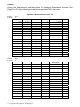
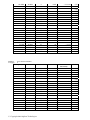
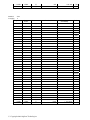
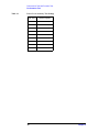
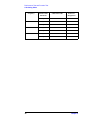
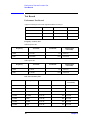
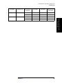
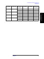
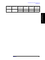
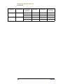
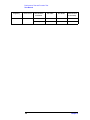
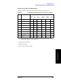
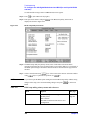
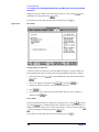
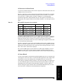
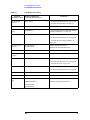
Change the Measurement Uncertainty value of Frequency Accuracy Test (Page 74) to the
following information and appended TAR to this report.
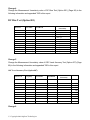
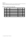
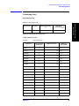
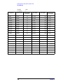
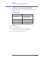
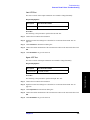
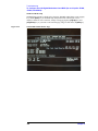
Frequency Accuracy Test
Without Option 1D5
Frequency
Test Limit
1 MHz
3 GHz
± 10 Hz
± 30 kHz
Test Result
TAR
Hz
kHz
Measurement
Uncertainty
± 0.491 Hz
± 0.369 kHz
TAR
Hz
kHz
Measurement
Uncertainty
± 0.003 Hz
± 0.008 kHz
20.4
81.5
With Option 1D5
Frequency
Test Limit
1 MHz
3 GHz
± 1 Hz
± 3 kHz
Test Result
3931
3859
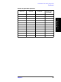
Change 2
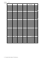
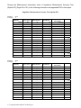
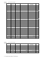
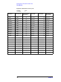
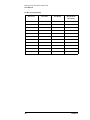
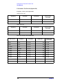
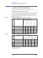
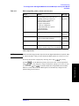
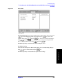
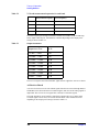
Change the Measurement Uncertainty value of OSC Level Accuracy Test (Page 74 to 75) to
the following information and appended TAR to this report.
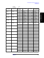
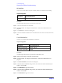
OSC Level Accuracy Test
Power Level
1 dBm
0 dBm
-7.9 dBm
-10 dBm
-15 dBm
-20 dBm
-25 dBm
-30 dBm
-35 dBm
-40 dBm
Frequency
1 GHz
3 GHz
3 GHz
300 MHz
1 MHz
50 MHz
1 GHz
10 MHz
2 GHz
100 MHz
C Copyright 2009 Agilent Technologies
○
Test Limit
± 2.00 dB
± 3.00 dB
± 3.00 dB
± 2.00 dB
± 2.00 dB
± 2.00 dB
± 2.00 dB
± 2.00 dB
± 3.00 dB
± 2.00 dB
Test Result
dB
dB
dB
dB
dB
dB
dB
dB
dB
dB
Measurement
Uncertainty
± 0.22 dB
± 0.35 dB
± 0.35 dB
± 0.26 dB
± 0.22 dB
± 0.24 dB
± 0.24 dB
± 0.22 dB
± 0.24 dB
± 0.27 dB
TAR
9.44
8.72
8.62
7.88
9.4
8.57
8.57
9.38
12.69
7.63
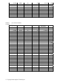
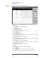
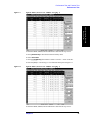
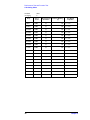
Change 3
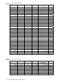
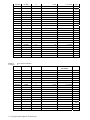
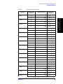
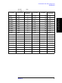
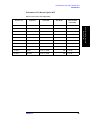
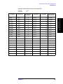
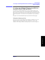
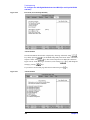
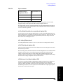
Change the Measurement Uncertainty value of Impedance Measurement Accuracy Test
(Page 76 to 87) to the following information and appended TAR to this report.
Impedance Measurement Accuracy Test
Standard:
Averaging:
Open
8
Frequency
1 MHz
10 MHz
100 MHz
200 MHz
300 MHz
500 MHz
600 MHz
800 MHz
1.0 GHz
1.3 GHz
1.6 GHz
1.8 GHz
2.0 GHz
2.2 GHz
2.4 GHz
2.6 GHz
2.8 GHz
3.0 GHz
Standard:
Averaging:
Short
8
Frequency
1 MHz
10 MHz
100 MHz
200 MHz
300 MHz
500 MHz
600 MHz
800 MHz
1.0 GHz
1.3 GHz
1.6 GHz
1.8 GHz
2.0 GHz
2.2 GHz
2.4 GHz
2.6 GHz
2.8 GHz
3.0 GHz
Power Level
Measurement
-3 dBm
-3 dBm
-3 dBm
-3 dBm
-3 dBm
-3 dBm
-3 dBm
-3 dBm
-3 dBm
-3 dBm
-3 dBm
-3 dBm
-3 dBm
-3 dBm
-3 dBm
-3 dBm
-3 dBm
-3 dBm
|Y|
|Y|
|Y|
|Y|
|Y|
|Y|
|Y|
|Y|
|Y|
|Y|
|Y|
|Y|
|Y|
|Y|
|Y|
|Y|
|Y|
|Y|
Power Level
Measurement
-3 dBm
-3 dBm
-3 dBm
-3 dBm
-3 dBm
-3 dBm
-3 dBm
-3 dBm
-3 dBm
-3 dBm
-3 dBm
-3 dBm
-3 dBm
-3 dBm
-3 dBm
-3 dBm
-3 dBm
-3 dBm
|Z|
|Z|
|Z|
|Z|
|Z|
|Z|
|Z|
|Z|
|Z|
|Z|
|Z|
|Z|
|Z|
|Z|
|Z|
|Z|
|Z|
|Z|
C Copyright 2009 Agilent Technologies
○
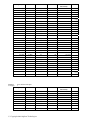
Test Result
μS
μS
μS
μS
μS
μS
μS
μS
μS
μS
μS
μS
μS
μS
μS
μS
μS
μS
Test Result
mΩ
mΩ
mΩ
mΩ
mΩ
mΩ
mΩ
mΩ
mΩ
mΩ
mΩ
mΩ
mΩ
mΩ
mΩ
mΩ
mΩ
mΩ
Measurement
Uncertainty
± 0.61 μS
± 0.46 μS
± 3.3 μS
± 6.5 μS
± 9.8 μS
± 17 μS
± 21 μS
± 28 μS
± 35 μS
± 46 μS
± 61 μS
± 69 μS
± 126 μS
± 140 μS
± 155 μS
± 171 μS
± 186 μS
± 203 μS
TAR
Measurement
Uncertainty
± 2.6 mΩ
± 3.6 mΩ
± 15 mΩ
± 26 mΩ
± 31 mΩ
± 51 mΩ
± 51 mΩ
± 51 mΩ
± 51 mΩ
± 101 mΩ
± 101 mΩ
± 101 mΩ
± 201 mΩ
± 201 mΩ
± 201 mΩ
± 201 mΩ
± 201 mΩ
± 201 mΩ
TAR
8.42
13.61
5.45
4.85
4.58
4.39
4.62
4.63
4.61
6.24
6.03
6.11
5.49
5.60
5.69
5.82
5.98
6.14
5.25
5.05
4.49
4.51
5.43
5.25
6.24
8.23
10.23
6.63
8.13
9.12
5.06
5.56
6.06
6.56
7.06
7.55
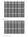
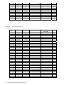
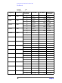
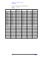
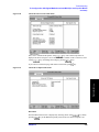
Standard:
Averaging:
50 Ω
8
Frequency
1 MHz
1 MHz
10 MHz
10 MHz
100 MHz
100 MHz
200 MHz
200 MHz
300 MHz
300 MHz
500 MHz
500 MHz
600 MHz
600 MHz
800 MHz
800 MHz
1.0 GHz
1.0 GHz
1.3 GHz
1.3 GHz
1.6 GHz
1.6 GHz
1.8 GHz
1.8 GHz
2.0 GHz
2.0 GHz
2.2 GHz
2.2 GHz
2.4 GHz
2.4 GHz
2.6 GHz
2.6 GHz
2.8 GHz
2.8 GHz
3.0 GHz
3.0 GHz
Power Level
Measurement
-3 dBm
-3 dBm
-3 dBm
-3 dBm
-3 dBm
-3 dBm
-3 dBm
-3 dBm
-3 dBm
-3 dBm
-3 dBm
-3 dBm
-3 dBm
-3 dBm
-3 dBm
-3 dBm
-3 dBm
-3 dBm
-3 dBm
-3 dBm
-3 dBm
-3 dBm
-3 dBm
-3 dBm
-3 dBm
-3 dBm
-3 dBm
-3 dBm
-3 dBm
-3 dBm
-3 dBm
-3 dBm
-3 dBm
-3 dBm
-3 dBm
-3 dBm
|Z|
θ
|Z|
θ
|Z|
θ
|Z|
θ
|Z|
θ
|Z|
θ
|Z|
θ
|Z|
θ
|Z|
θ
|Z|
θ
|Z|
θ
|Z|
θ
|Z|
θ
|Z|
θ
|Z|
θ
|Z|
θ
|Z|
θ
|Z|
θ
C Copyright 2009 Agilent Technologies
○
Test Result
Ω
mrad
Ω
mrad
Ω
mrad
Ω
mrad
Ω
mrad
Ω
mrad
Ω
mrad
Ω
mrad
Ω
mrad
Ω
mrad
Ω
mrad
Ω
mrad
Ω
mrad
Ω
mrad
Ω
mrad
Ω
mrad
Ω
mrad
Ω
mrad
Measurement
Uncertainty
± 0.09 Ω
± 1.7 mrad
± 0.09 Ω
± 1.7 mrad
± 0.09 Ω
± 1.7 mrad
± 0.11 Ω
± 2.2 mrad
± 0.14 Ω
± 2.7 mrad
± 0.19 Ω
± 3.7 mrad
± 0.23 Ω
± 4.6 mrad
± 0.23 Ω
± 4.6 mrad
± 0.23 Ω
± 4.6 mrad
± 0.24 Ω
± 4.7 mrad
± 0.24 Ω
± 4.8 mrad
± 0.24 Ω
± 4.6 mrad
± 0.51 Ω
± 10.1 mrad
± 0.51 Ω
± 10.2 mrad
± 0.51 Ω
± 10.1 mrad
± 0.51 Ω
± 10.2 mrad
± 0.53 Ω
± 10.2 mrad
± 0.53 Ω
± 10.9 mrad
TAR
4.17
4.20
4.26
4.28
5.09
5.10
5.30
5.29
4.92
4.93
4.44
4.44
4.70
4.69
5.37
5.36
5.99
6.00
9.60
9.65
10.43
10.47
11.32
11.49
8.00
8.01
8.20
8.21
8.58
8.59
8.84
8.84
8.79
9.08
9.07
8.83
Standard:
Averaging:
10 cm Airline with Open
8
Frequency
Power Level
1 MHz
1 MHz
10 MHz
10 MHz
100 MHz
100 MHz
200 MHz
200 MHz
300 MHz
300 MHz
500 MHz
500 MHz
600 MHz
600 MHz
800 MHz
800 MHz
1.0 GHz
1.0 GHz
1.6 GHz
1.6 GHz
1.8 GHz
1.8 GHz
2.0 GHz
2.0 GHz
2.2 GHz
2.2 GHz
2.4 GHz
2.4 GHz
2.6 GHz
2.6 GHz
3.0 GHz
3.0 GHz
Standard:
Averaging:
-3 dBm
-3 dBm
-3 dBm
-3 dBm
-3 dBm
-3 dBm
-3 dBm
-3 dBm
-3 dBm
-3 dBm
-3 dBm
-3 dBm
-3 dBm
-3 dBm
-3 dBm
-3 dBm
-3 dBm
-3 dBm
-3 dBm
-3 dBm
-3 dBm
-3 dBm
-3 dBm
-3 dBm
-3 dBm
-3 dBm
-3 dBm
-3 dBm
-3 dBm
-3 dBm
-3 dBm
-3 dBm
10 cm Airline with Open
1
Frequency
Power Level
1 MHz
1 MHz
10 MHz
10 MHz
100 MHz
100 MHz
200 MHz
200 MHz
Measurement
|Z|
θ
|Z|
θ
|Z|
θ
|Z|
θ
|Z|
θ
|Z|
θ
|Z|
θ
|Z|
θ
|Z|
θ
|Z|
θ
|Z|
θ
|Z|
θ
|Z|
θ
|Z|
θ
|Z|
θ
|Z|
θ
Measurement
-20 dBm
-20 dBm
-20 dBm
-20 dBm
-20 dBm
-20 dBm
-20 dBm
-20 dBm
C Copyright 2009 Agilent Technologies
○
|Z|
θ
|Z|
θ
|Z|
θ
|Z|
θ
Test Result
Ω
mrad
Ω
mrad
Ω
mrad
Ω
mrad
Ω
mrad
Ω
mrad
Ω
mrad
Ω
mrad
Ω
mrad
Ω
mrad
Ω
mrad
Ω
mrad
Ω
mrad
Ω
mrad
Ω
mrad
Ω
mrad
Test Result
Ω
mrad
Ω
mrad
Ω
mrad
Ω
mrad
Measurement
Uncertainty
± 254 Ω
± 17.6 mrad
± 4.3 Ω
± 2.0 mrad
± 0.42 Ω
± 2.0 mrad
± 0.22 Ω
± 2.2 mrad
± 0.16 Ω
± 2.6 mrad
± 0.09 Ω
± 3.7 mrad
± 0.09 Ω
± 8.7 mrad
± 0.12 Ω
± 8.7 mrad
± 0.23 Ω
± 5.2 mrad
± 0.72 Ω
± 8.4 mrad
± 0.29 Ω
± 8.5 mrad
± 0.10 Ω
± 14.3 mrad
± 0.23 Ω
± 12.8 mrad
± 0.64 Ω
± 12.5 mrad
± 2.2 Ω
± 14.4 mrad
± 1.1 Ω
± 13.8 mrad
TAR
Measurement
Uncertainty
± 1771 Ω
± 50.6 mrad
± 7.7 Ω
± 5.3 mrad
± 0.42 Ω
± 2.1 mrad
± 0.22 Ω
± 2.2 mrad
TAR
10.13
6.71
10.03
9.94
5.22
5.27
5.47
5.50
4.96
5.01
5.61
5.67
5.12
5.17
5.02
5.03
5.50
5.51
5.83
5.86
6.88
6.92
14.69
14.81
9.24
9.27
6.92
6.93
6.88
6.89
6.71
6.75
8.18
13.12
21.20
14.20
8.05
7.50
6.76
6.86
300 MHz
300 MHz
500 MHz
500 MHz
600 MHz
600 MHz
800 MHz
800 MHz
1.0 GHz
1.0 GHz
1.6 GHz
1.6 GHz
1.8 GHz
1.8 GHz
2.0 GHz
2.0 GHz
2.2 GHz
2.2 GHz
2.4 GHz
2.4 GHz
2.6 GHz
2.6 GHz
3.0 GHz
3.0 GHz
Standard:
Averaging:
-20 dBm
-20 dBm
-20 dBm
-20 dBm
-20 dBm
-20 dBm
-20 dBm
-20 dBm
-20 dBm
-20 dBm
-20 dBm
-20 dBm
-20 dBm
-20 dBm
-20 dBm
-20 dBm
-20 dBm
-20 dBm
-20 dBm
-20 dBm
-20 dBm
-20 dBm
-20 dBm
-20 dBm
|Z|
θ
|Z|
θ
|Z|
θ
|Z|
θ
|Z|
θ
|Z|
θ
|Z|
θ
|Z|
θ
|Z|
θ
|Z|
θ
|Z|
θ
|Z|
θ
Ω
mrad
Ω
mrad
Ω
mrad
Ω
mrad
Ω
mrad
Ω
mrad
Ω
mrad
Ω
mrad
Ω
mrad
Ω
mrad
Ω
mrad
Ω
mrad
± 0.16 Ω
± 2.6 mrad
± 0.09 Ω
± 3.7 mrad
± 0.09 Ω
± 8.7 mrad
± 0.12 Ω
± 8.7 mrad
± 0.23 Ω
± 5.2 mrad
± 0.72 Ω
± 8.4 mrad
± 0.29 Ω
± 8.5 mrad
± 0.10 Ω
± 14.4 mrad
± 0.23 Ω
± 12.8 mrad
± 0.64 Ω
± 12.5 mrad
± 2.2 Ω
± 14.4 mrad
± 1.1 Ω
± 13.9 mrad
Test Result
Measurement
Uncertainty
± 0.002 Ω
± 19.4 mrad
± 0.005 Ω
± 4.2 mrad
± 0.03 Ω
± 2.5 mrad
± 0.07 Ω
± 3.0 mrad
± 0.11 Ω
± 3.0 mrad
± 0.31 Ω
± 3.5 mrad
± 0.77 Ω
± 5.0 mrad
± 0.45 Ω
± 5.2 mrad
± 0.19 Ω
± 8.3 mrad
5.79
5.80
6.19
6.26
5.58
5.63
5.36
5.37
5.89
5.89
6.14
6.16
7.12
7.15
14.99
15.19
9.41
9.46
7.08
7.09
7.16
7.16
6.88
6.91
10 cm Airline with Short
8
Frequency
1 MHz
1 MHz
10 MHz
10 MHz
100 MHz
100 MHz
200 MHz
200 MHz
300 MHz
300 MHz
500 MHz
500 MHz
600 MHz
600 MHz
1.0 GHz
1.0 GHz
1.3 GHz
1.3 GHz
Power Level
Measurement
-3 dBm
-3 dBm
-3 dBm
-3 dBm
-3 dBm
-3 dBm
-3 dBm
-3 dBm
-3 dBm
-3 dBm
-3 dBm
-3 dBm
-3 dBm
-3 dBm
-3 dBm
-3 dBm
-3 dBm
-3 dBm
|Z|
θ
|Z|
θ
|Z|
θ
|Z|
θ
|Z|
θ
|Z|
θ
|Z|
θ
|Z|
θ
|Z|
θ
C Copyright 2009 Agilent Technologies
○
Ω
mrad
Ω
mrad
Ω
mrad
Ω
mrad
Ω
mrad
Ω
mrad
Ω
mrad
Ω
mrad
Ω
mrad
TAR
7.50
6.47
5.63
5.60
5.13
5.13
4.63
4.62
4.67
4.68
4.57
4.57
4.92
4.91
5.20
5.22
6.98
7.01
1.6 GHz
1.6 GHz
1.8 GHz
1.8 GHz
2.0 GHz
2.0 GHz
2.4 GHz
2.4 GHz
2.6 GHz
2.6 GHz
2.8 GHz
2.8 GHz
Standard:
Averaging:
-3 dBm
-3 dBm
-3 dBm
-3 dBm
-3 dBm
-3 dBm
-3 dBm
-3 dBm
-3 dBm
-3 dBm
-3 dBm
-3 dBm
10 cm Airline with Short
1
Frequency
Power Level
1 MHz
1 MHz
10 MHz
10 MHz
100 MHz
100 MHz
200 MHz
200 MHz
300 MHz
300 MHz
500 MHz
500 MHz
600 MHz
600 MHz
1.0 GHz
1.0 GHz
1.3 GHz
1.3 GHz
1.6 GHz
1.6 GHz
1.8 GHz
1.8 GHz
2.0 GHz
2.0 GHz
2.4 GHz
2.4 GHz
2.6 GHz
2.6 GHz
2.8 GHz
2.8 GHz
|Z|
θ
|Z|
θ
|Z|
θ
|Z|
θ
|Z|
θ
|Z|
θ
Measurement
-40 dBm
-40 dBm
-40 dBm
-40 dBm
-40 dBm
-40 dBm
-40 dBm
-40 dBm
-40 dBm
-40 dBm
-40 dBm
-40 dBm
-40 dBm
-40 dBm
-40 dBm
-40 dBm
-40 dBm
-40 dBm
-40 dBm
-40 dBm
-40 dBm
-40 dBm
-40 dBm
-40 dBm
-40 dBm
-40 dBm
-40 dBm
-40 dBm
-40 dBm
-40 dBm
C Copyright 2009 Agilent Technologies
○
|Z|
θ
|Z|
θ
|Z|
θ
|Z|
θ
|Z|
θ
|Z|
θ
|Z|
θ
|Z|
θ
|Z|
θ
|Z|
θ
|Z|
θ
|Z|
θ
|Z|
θ
|Z|
θ
|Z|
θ
Ω
mrad
Ω
mrad
Ω
mrad
Ω
mrad
Ω
mrad
Ω
mrad
± 0.12 Ω
± 10.8 mrad
± 0.31 Ω
± 8.3 mrad
± 0.91 Ω
± 10.4 mrad
± 2.06 Ω
± 13.6 mrad
± 0.74 Ω
± 13.4 mrad
± 0.30 Ω
± 13.6 mrad
Test Result
Measurement
Uncertainty
± 0.010 Ω
± 68.1 mrad
± 0.011 Ω
± 8.5 mrad
± 0.03 Ω
± 2.9 mrad
± 0.07 Ω
± 3.0 mrad
± 0.12 Ω
± 3.0 mrad
± 0.31 Ω
± 3.6 mrad
± 0.80 Ω
± 5.1 mrad
± 0.45 Ω
± 5.2 mrad
± 0.19 Ω
± 8.3 mrad
± 0.12 Ω
± 11.0 mrad
± 0.31 Ω
± 8.4 mrad
± 0.92 Ω
± 10.4 mrad
± 2.06 Ω
± 13.6 mrad
± 0.74 Ω
± 13.4 mrad
± 0.30 Ω
± 13.7 mrad
Ω
mrad
Ω
mrad
Ω
mrad
Ω
mrad
Ω
mrad
Ω
mrad
Ω
mrad
Ω
mrad
Ω
mrad
Ω
mrad
Ω
mrad
Ω
mrad
Ω
mrad
Ω
mrad
Ω
mrad
9.42
9.43
6.81
6.84
7.74
7.76
7.01
7.02
6.64
6.64
8.87
8.90
TAR
10.74
8.87
10.84
8.87
9.41
8.87
7.69
8.87
7.35
8.87
7.31
8.87
6.52
8.87
6.29
8.87
7.61
8.87
10.07
8.87
7.32
8.87
8.20
8.87
7.65
8.87
6.98
8.87
9.23
8.87
Change 4
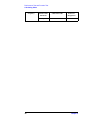
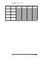
Change the Measurement Uncertainty value of DC Bias Test (Option 001) (Page 88) to the
following information and appended TAR to this report.
DC Bias Test (Option 001)
Bias Level
-40 V
-4 V
0V
4V
40 V
-50 mA
-4 mA
-100 μA
100 μA
4 mA
50 mA
Test Limit
Measurement
Uncertainty
Test Result
± 46.00 mV
± 10.00 mV
± 6.00 mV
± 10.00 mV
± 46.00 mV
± 120.0 μA
± 28.0 μA
± 20.2 μA
± 20.2 μA
± 28.0 μA
± 120.0 μA
mV
μV
μV
μV
mV
μA
μA
μA
μA
μA
μA
TAR
46.50
174.60
216.90
205.80
47.39
12.86
24.11
21.07
17.44
24.48
13.28
± 0.99 mV
± 57.3 μV
± 27.8 μV
± 48.6 μV
± 0.98 mV
± 9.4 μA
± 1.2 μA
± 1.0 μA
± 1.2 μA
± 1.2 μA
± 9.1 μA
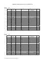
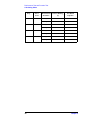
Change 5
Change the Measurement Uncertainty value of OSC Level Accuracy Test (Option 007) (Page
89) to the following information and appended TAR to this report.
OSC Level Accuracy Test (Option 007)
Power Level
1 dBm
0 dBm
-7.9 dBm
-10 dBm
-15 dBm
-20 dBm
-25 dBm
-30 dBm
-35 dBm
-40 dBm
Frequency
Test Limit
1 GHz -4.00dB/+2.00dB
3 GHz
3 GHz
300 MHz
1 MHz
50 MHz
1 GHz
10 MHz
2 GHz
100 MHz
-6.00dB/+3.00dB
-6.00dB/+3.00dB
-4.00dB/+2.00dB
-4.00dB/+2.00dB
-4.00dB/+2.00dB
-4.00dB/+2.00dB
-4.00dB/+2.00dB
-6.00dB/+3.00dB
-4.00dB/+2.00dB
Change 6
C Copyright 2009 Agilent Technologies
○
dB
Measurement
Uncertainty
± 0.22 dB
dB
dB
dB
dB
dB
dB
dB
dB
dB
± 0.35 dB
± 0.35 dB
± 0.26 dB
± 0.22 dB
± 0.24 dB
± 0.24 dB
± 0.22 dB
± 0.24 dB
± 0.27 dB
Test Result
TAR
9.44
8.72
8.62
7.88
9.40
8.57
8.57
9.38
12.69
7.63
Change the Measurement Uncertainty value of Impedance Measurement Accuracy Test
(Option 007) (Page 90 to 101) to the following information and appended TAR to this report.
Impedance Measurement Accuracy Test (Option 007)
Standard:
Averaging:
Open
8
Frequency
1 MHz
10 MHz
100 MHz
200 MHz
300 MHz
500 MHz
600 MHz
800 MHz
1.0 GHz
1.3 GHz
1.6 GHz
1.8 GHz
2.0 GHz
2.2 GHz
2.4 GHz
2.6 GHz
2.8 GHz
3.0 GHz
Standard:
Averaging:
Power Level
Measurement
-3 dBm
-3 dBm
-3 dBm
-3 dBm
-3 dBm
-3 dBm
-3 dBm
-3 dBm
-3 dBm
-3 dBm
-3 dBm
-3 dBm
-3 dBm
-3 dBm
-3 dBm
-3 dBm
-3 dBm
-3 dBm
|Y|
|Y|
|Y|
|Y|
|Y|
|Y|
|Y|
|Y|
|Y|
|Y|
|Y|
|Y|
|Y|
|Y|
|Y|
|Y|
|Y|
|Y|
Test Result
μS
μS
μS
μS
μS
μS
μS
μS
μS
μS
μS
μS
μS
μS
μS
μS
μS
μS
Measurement
Uncertainty
± 0.38 μS
± 0.80 μS
± 3.4 μS
± 6.6 μS
± 9.8 μS
± 17 μS
± 21 μS
± 28 μS
± 35 μS
± 46 μS
± 61 μS
± 70 μS
± 126 μS
± 140 μS
± 156 μS
± 171 μS
± 186 μS
± 205 μS
TAR
Measurement
Uncertainty
± 3.1 mΩ
± 3.6 mΩ
± 15 mΩ
± 26 mΩ
± 31 mΩ
± 51 mΩ
± 51 mΩ
± 51 mΩ
± 51 mΩ
± 101 mΩ
± 101 mΩ
± 101 mΩ
± 201 mΩ
± 201 mΩ
± 201 mΩ
± 201 mΩ
± 201 mΩ
TAR
32.55
16.85
7.57
6.13
5.53
5.09
4.94
4.90
4.81
6.40
6.15
6.16
5.55
5.66
5.73
5.86
6.04
6.14
Short
8
Frequency
1 MHz
10 MHz
100 MHz
200 MHz
300 MHz
500 MHz
600 MHz
800 MHz
1.0 GHz
1.3 GHz
1.6 GHz
1.8 GHz
2.0 GHz
2.2 GHz
2.4 GHz
2.6 GHz
2.8 GHz
Power Level
Measurement
-3 dBm
-3 dBm
-3 dBm
-3 dBm
-3 dBm
-3 dBm
-3 dBm
-3 dBm
-3 dBm
-3 dBm
-3 dBm
-3 dBm
-3 dBm
-3 dBm
-3 dBm
-3 dBm
-3 dBm
C Copyright 2009 Agilent Technologies
○
|Z|
|Z|
|Z|
|Z|
|Z|
|Z|
|Z|
|Z|
|Z|
|Z|
|Z|
|Z|
|Z|
|Z|
|Z|
|Z|
|Z|
Test Result
mΩ
mΩ
mΩ
mΩ
mΩ
mΩ
mΩ
mΩ
mΩ
mΩ
mΩ
mΩ
mΩ
mΩ
mΩ
mΩ
mΩ
10.09
9.79
5.70
5.16
5.97
5.58
6.57
8.56
10.57
6.79
8.29
9.28
5.15
5.64
6.15
6.64
7.14
3.0 GHz
Standard:
Averaging:
|Z|
mΩ
± 201 mΩ
7.65
50 Ω
8
Frequency
1 MHz
1 MHz
10 MHz
10 MHz
100 MHz
100 MHz
200 MHz
200 MHz
300 MHz
300 MHz
500 MHz
500 MHz
600 MHz
600 MHz
800 MHz
800 MHz
1.0 GHz
1.0 GHz
1.3 GHz
1.3 GHz
1.6 GHz
1.6 GHz
1.8 GHz
1.8 GHz
2.0 GHz
2.0 GHz
2.2 GHz
2.2 GHz
2.4 GHz
2.4 GHz
2.6 GHz
2.6 GHz
2.8 GHz
2.8 GHz
3.0 GHz
3.0 GHz
Standard:
Averaging:
-3 dBm
Power Level
Measurement
-3 dBm
-3 dBm
-3 dBm
-3 dBm
-3 dBm
-3 dBm
-3 dBm
-3 dBm
-3 dBm
-3 dBm
-3 dBm
-3 dBm
-3 dBm
-3 dBm
-3 dBm
-3 dBm
-3 dBm
-3 dBm
-3 dBm
-3 dBm
-3 dBm
-3 dBm
-3 dBm
-3 dBm
-3 dBm
-3 dBm
-3 dBm
-3 dBm
-3 dBm
-3 dBm
-3 dBm
-3 dBm
-3 dBm
-3 dBm
-3 dBm
-3 dBm
10 cm Airline with Open
8
C Copyright 2009 Agilent Technologies
○
|Z|
θ
|Z|
θ
|Z|
θ
|Z|
θ
|Z|
θ
|Z|
θ
|Z|
θ
|Z|
θ
|Z|
θ
|Z|
θ
|Z|
θ
|Z|
θ
|Z|
θ
|Z|
θ
|Z|
θ
|Z|
θ
|Z|
θ
|Z|
θ
Test Result
Ω
mrad
Ω
mrad
Ω
mrad
Ω
mrad
Ω
mrad
Ω
mrad
Ω
mrad
Ω
mrad
Ω
mrad
Ω
mrad
Ω
mrad
Ω
mrad
Ω
mrad
Ω
mrad
Ω
mrad
Ω
mrad
Ω
mrad
Ω
mrad
Measurement
Uncertainty
± 0.09 Ω
± 1.7 mrad
± 0.09 Ω
± 1.7 mrad
± 0.09 Ω
± 1.7 mrad
± 0.11 Ω
± 2.2 mrad
± 0.14 Ω
± 2.7 mrad
± 0.19 Ω
± 3.7 mrad
± 0.23 Ω
± 4.6 mrad
± 0.23 Ω
± 4.6 mrad
± 0.24 Ω
± 4.6 mrad
± 0.24 Ω
± 4.7 mrad
± 0.24 Ω
± 4.8 mrad
± 0.24 Ω
± 4.8 mrad
± 0.51 Ω
± 10.2 mrad
± 0.51 Ω
± 10.3 mrad
± 0.51 Ω
± 10.2 mrad
± 0.51 Ω
± 10.3 mrad
± 0.51 Ω
± 10.3 mrad
± 0.51 Ω
± 10.3 mrad
TAR
5.51
8.87
5.60
8.87
6.39
8.87
6.54
8.87
5.94
8.87
5.19
8.87
4.84
8.87
5.52
8.87
6.12
8.87
9.74
8.87
10.51
8.87
11.49
8.87
8.07
8.87
8.27
8.87
8.65
8.87
8.90
8.87
9.19
8.87
9.55
8.87
Frequency
1 MHz
1 MHz
10 MHz
10 MHz
100 MHz
100 MHz
200 MHz
200 MHz
300 MHz
300 MHz
500 MHz
500 MHz
600 MHz
600 MHz
800 MHz
800 MHz
1.0 GHz
1.0 GHz
1.6 GHz
1.6 GHz
1.8 GHz
1.8 GHz
2.0 GHz
2.0 GHz
2.2 GHz
2.2 GHz
2.4 GHz
2.4 GHz
2.6 GHz
2.6 GHz
3.0 GHz
3.0 GHz
Standard:
Averaging:
Power Level
Measurement
-3 dBm
-3 dBm
-3 dBm
-3 dBm
-3 dBm
-3 dBm
-3 dBm
-3 dBm
-3 dBm
-3 dBm
-3 dBm
-3 dBm
-3 dBm
-3 dBm
-3 dBm
-3 dBm
-3 dBm
-3 dBm
-3 dBm
-3 dBm
-3 dBm
-3 dBm
-3 dBm
-3 dBm
-3 dBm
-3 dBm
-3 dBm
-3 dBm
-3 dBm
-3 dBm
-3 dBm
-3 dBm
|Z|
θ
|Z|
θ
|Z|
θ
|Z|
θ
|Z|
θ
|Z|
θ
|Z|
θ
|Z|
θ
|Z|
θ
|Z|
θ
|Z|
θ
|Z|
θ
|Z|
θ
|Z|
θ
|Z|
θ
|Z|
θ
10 cm Airline with Open
1
Frequency
Power Level
1 MHz
1 MHz
10 MHz
10 MHz
100 MHz
100 MHz
200 MHz
200 MHz
300 MHz
-20 dBm
-20 dBm
-20 dBm
-20 dBm
-20 dBm
-20 dBm
-20 dBm
-20 dBm
-20 dBm
C Copyright 2009 Agilent Technologies
○
Measurement
|Z|
θ
|Z|
θ
|Z|
θ
|Z|
θ
|Z|
Test Result
Ω
mrad
Ω
mrad
Ω
mrad
Ω
mrad
Ω
mrad
Ω
mrad
Ω
mrad
Ω
mrad
Ω
mrad
Ω
mrad
Ω
mrad
Ω
mrad
Ω
mrad
Ω
mrad
Ω
mrad
Ω
mrad
Test Result
Ω
mrad
Ω
mrad
Ω
mrad
Ω
mrad
Ω
Measurement
Uncertainty
± 296 Ω
± 10.3 mrad
± 5.3 Ω
± 2.3 mrad
± 0.42 Ω
± 2.0 mrad
± 0.22 Ω
± 2.2 mrad
± 0.16 Ω
± 2.6 mrad
± 0.09 Ω
± 3.8 mrad
± 0.09 Ω
± 8.7 mrad
± 0.12 Ω
± 8.7 mrad
± 0.23 Ω
± 5.2 mrad
± 0.72 Ω
± 8.4 mrad
± 0.29 Ω
± 8.5 mrad
± 0.10 Ω
± 14.4 mrad
± 0.23 Ω
± 12.8 mrad
± 0.64 Ω
± 12.6 mrad
± 2.2 Ω
± 14.4 mrad
± 1.1 Ω
± 13.9 mrad
TAR
Measurement
Uncertainty
± 969 Ω
± 61.5 mrad
± 10.5 Ω
± 3.4 mrad
± 0.42 Ω
± 2.0 mrad
± 0.23 Ω
± 2.2 mrad
± 0.17 Ω
TAR
20.13
8.87
15.15
8.87
6.79
8.87
6.75
8.87
5.94
8.87
6.38
8.87
5.20
8.87
5.12
8.87
5.60
8.87
5.92
8.87
6.93
8.87
14.54
8.87
9.31
8.87
6.95
8.87
6.94
8.87
6.75
8.87
19.90
8.87
20.37
8.87
9.98
8.87
7.96
8.87
6.67
300 MHz
500 MHz
500 MHz
600 MHz
600 MHz
800 MHz
800 MHz
1.0 GHz
1.0 GHz
1.6 GHz
1.6 GHz
1.8 GHz
1.8 GHz
2.0 GHz
2.0 GHz
2.2 GHz
2.2 GHz
2.4 GHz
2.4 GHz
2.6 GHz
2.6 GHz
3.0 GHz
3.0 GHz
Standard:
Averaging:
-20 dBm
-20 dBm
-20 dBm
-20 dBm
-20 dBm
-20 dBm
-20 dBm
-20 dBm
-20 dBm
-20 dBm
-20 dBm
-20 dBm
-20 dBm
-20 dBm
-20 dBm
-20 dBm
-20 dBm
-20 dBm
-20 dBm
-20 dBm
-20 dBm
-20 dBm
-20 dBm
10 cm Airline with Short
8
Frequency
Power Level
1 MHz
1 MHz
10 MHz
10 MHz
100 MHz
100 MHz
200 MHz
200 MHz
300 MHz
300 MHz
500 MHz
500 MHz
600 MHz
600 MHz
1.0 GHz
1.0 GHz
1.3 GHz
1.3 GHz
1.6 GHz
1.6 GHz
-3 dBm
-3 dBm
-3 dBm
-3 dBm
-3 dBm
-3 dBm
-3 dBm
-3 dBm
-3 dBm
-3 dBm
-3 dBm
-3 dBm
-3 dBm
-3 dBm
-3 dBm
-3 dBm
-3 dBm
-3 dBm
-3 dBm
-3 dBm
C Copyright 2009 Agilent Technologies
○
θ
|Z|
θ
|Z|
θ
|Z|
θ
|Z|
θ
|Z|
θ
|Z|
θ
|Z|
θ
|Z|
θ
|Z|
θ
|Z|
θ
|Z|
θ
Measurement
|Z|
θ
|Z|
θ
|Z|
θ
|Z|
θ
|Z|
θ
|Z|
θ
|Z|
θ
|Z|
θ
|Z|
θ
|Z|
θ
mrad
Ω
mrad
Ω
mrad
Ω
mrad
Ω
mrad
Ω
mrad
Ω
mrad
Ω
mrad
Ω
mrad
Ω
mrad
Ω
mrad
Ω
mrad
Test Result
Ω
mrad
Ω
mrad
Ω
mrad
Ω
mrad
Ω
mrad
Ω
mrad
Ω
mrad
Ω
mrad
Ω
mrad
Ω
mrad
± 2.6 mrad
± 0.09 Ω
± 3.8 mrad
± 0.09 Ω
± 8.7 mrad
± 0.12 Ω
± 8.8 mrad
± 0.23 Ω
± 5.2 mrad
± 0.72 Ω
± 8.4 mrad
± 0.29 Ω
± 8.5 mrad
± 0.10 Ω
± 14.3 mrad
± 0.23 Ω
± 12.8 mrad
± 0.64 Ω
± 12.6 mrad
± 2.2 Ω
± 14.4 mrad
± 1.1 Ω
± 13.9 mrad
Measurement
Uncertainty
± 0.002 Ω
± 27.2 mrad
± 0.005 Ω
± 4.4 mrad
± 0.03 Ω
± 2.5 mrad
± 0.07 Ω
± 3.0 mrad
± 0.11 Ω
± 3.0 mrad
± 0.31 Ω
± 3.5 mrad
± 0.77 Ω
± 5.0 mrad
± 0.46 Ω
± 5.2 mrad
± 0.19 Ω
± 8.3 mrad
± 0.12 Ω
± 10.9 mrad
8.87
7.06
8.87
5.78
8.87
5.50
8.87
6.01
8.87
6.26
8.87
7.19
8.87
14.90
8.87
9.54
8.87
7.13
8.87
7.24
8.87
6.94
8.87
TAR
16.85
8.87
9.80
8.87
6.41
8.87
5.62
8.87
5.61
8.87
5.36
8.87
5.15
8.87
5.31
8.87
7.10
8.87
9.55
8.87
1.8 GHz
1.8 GHz
2.0 GHz
2.0 GHz
2.4 GHz
2.4 GHz
2.6 GHz
2.6 GHz
2.8 GHz
2.8 GHz
Standard:
Averaging:
-3 dBm
-3 dBm
-3 dBm
-3 dBm
-3 dBm
-3 dBm
-3 dBm
-3 dBm
-3 dBm
-3 dBm
10 cm Airline with Short
1
Frequency
Power Level
1 MHz
1 MHz
10 MHz
10 MHz
100 MHz
100 MHz
200 MHz
200 MHz
300 MHz
300 MHz
500 MHz
500 MHz
600 MHz
600 MHz
1.0 GHz
1.0 GHz
1.3 GHz
1.3 GHz
1.6 GHz
1.6 GHz
1.8 GHz
1.8 GHz
2.0 GHz
2.0 GHz
2.4 GHz
2.4 GHz
2.6 GHz
2.6 GHz
2.8 GHz
2.8 GHz
-40 dBm
-40 dBm
-40 dBm
-40 dBm
-40 dBm
-40 dBm
-40 dBm
-40 dBm
-40 dBm
-40 dBm
-40 dBm
-40 dBm
-40 dBm
-40 dBm
-40 dBm
-40 dBm
-40 dBm
-40 dBm
-40 dBm
-40 dBm
-40 dBm
-40 dBm
-40 dBm
-40 dBm
-40 dBm
-40 dBm
-40 dBm
-40 dBm
-40 dBm
-40 dBm
C Copyright 2009 Agilent Technologies
○
|Z|
θ
|Z|
θ
|Z|
θ
|Z|
θ
|Z|
θ
Measurement
|Z|
θ
|Z|
θ
|Z|
θ
|Z|
θ
|Z|
θ
|Z|
θ
|Z|
θ
|Z|
θ
|Z|
θ
|Z|
θ
|Z|
θ
|Z|
θ
|Z|
θ
|Z|
θ
|Z|
θ
Ω
mrad
Ω
mrad
Ω
mrad
Ω
mrad
Ω
mrad
Test Result
Ω
mrad
Ω
mrad
Ω
mrad
Ω
mrad
Ω
mrad
Ω
mrad
Ω
mrad
Ω
mrad
Ω
mrad
Ω
mrad
Ω
mrad
Ω
mrad
Ω
mrad
Ω
mrad
Ω
mrad
± 0.31 Ω
± 8.4 mrad
± 0.91 Ω
± 10.4 mrad
± 2.07 Ω
± 13.6 mrad
± 0.74 Ω
± 13.4 mrad
± 0.30 Ω
± 13.6 mrad
Measurement
Uncertainty
± 0.007 Ω
± 89.7 mrad
± 0.008 Ω
± 13.7 mrad
± 0.04 Ω
± 2.7 mrad
± 0.07 Ω
± 3.1 mrad
± 0.12 Ω
± 3.0 mrad
± 0.31 Ω
± 3.6 mrad
± 0.78 Ω
± 5.1 mrad
± 0.45 Ω
± 5.3 mrad
± 0.19 Ω
± 8.3 mrad
± 0.12 Ω
± 10.9 mrad
± 0.31 Ω
± 8.4 mrad
± 0.92 Ω
± 10.5 mrad
± 2.06 Ω
± 13.7 mrad
± 0.74 Ω
± 13.4 mrad
± 0.30 Ω
± 13.6 mrad
6.89
8.87
7.77
8.87
7.06
8.87
6.69
8.87
8.99
8.87
TAR
23.42
8.87
21.07
8.87
11.23
8.87
9.37
8.87
8.85
8.87
8.90
8.87
7.98
8.87
7.30
8.87
7.93
8.87
10.60
8.87
7.59
8.87
8.44
8.87
7.89
8.87
7.13
8.87
9.49
8.87
Change 7
Change the Measurement Uncertainty value of Frequency Accuracy Test (Option 010) (Page
102) to the following information and appended TAR to this report.
Frequency Accuracy Test (Option 010)
Without Option 1D5
Frequency
Test Limit
Test Result
1 MHz
3 GHz
± 10 Hz
± 30 kHz
Hz
kHz
Frequency
Test Limit
Test Result
1 MHz
3 GHz
± 1 Hz
± 3 kHz
Hz
kHz
Measurement
Uncertainty
± 0.029 Hz
± 0.085 kHz
TAR
Measurement
Uncertainty
± 0.003 Hz
± 0.008 kHz
TAR
351.40
354.90
With Option 1D5
4101.90
3822.90
Change 8
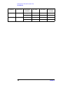
Change the Measurement Uncertainty value of OSC Level Accuracy Test (Option 010) (Page
102) to the following information and appended TAR to this report.
Power
Level
1 dBm
0 dBm
-7.9 dBm
-10 dBm
-15 dBm
-20 dBm
-25 dBm
-30 dBm
-35 dBm
-40 dBm
Frequency
1 GHz
3 GHz
3 GHz
300 MHz
1 MHz
50 MHz
1 GHz
10 MHz
2 GHz
100 MHz
Test Limit
± 3.50 dB
± 5.60 dB
± 5.60 dB
± 3.50 dB
± 3.50 dB
± 3.50 dB
± 3.50 dB
± 3.50 dB
± 5.60 dB
± 3.50 dB
Test Result
dB
dB
dB
dB
dB
dB
dB
dB
dB
dB
Measurement
Uncertainty
± 0.22 dB
± 0.35 dB
± 0.35 dB
± 0.26 dB
± 0.22 dB
± 0.24 dB
± 0.24 dB
± 0.22 dB
± 0.24 dB
± 0.27 dB
TAR
16.51
16.28
16.08
13.79
16.44
14.99
14.99
16.42
23.68
13.35
Change 9
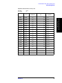
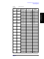
Change the Measurement Uncertainty value of Impedance Measurement Accuracy Test
(Option 010) (Page 103 to 114) to the following information and appended TAR to this report.
C Copyright 2009 Agilent Technologies
○
Impedance Measurement Accuracy Test (Option 010)
Standard:
Open
Averaging: 8
Frequency
1 MHz
10 MHz
100 MHz
200 MHz
300 MHz
500 MHz
600 MHz
800 MHz
1.0 GHz
1.3 GHz
1.6 GHz
1.8 GHz
2.0 GHz
2.2 GHz
2.4 GHz
2.6 GHz
2.8 GHz
3.0 GHz
Standard:
Short
Averaging: 8
Frequency
1 MHz
10 MHz
100 MHz
200 MHz
300 MHz
500 MHz
600 MHz
800 MHz
1.0 GHz
1.3 GHz
1.6 GHz
1.8 GHz
2.0 GHz
2.2 GHz
2.4 GHz
2.6 GHz
Power
Level
-3 dBm
-3 dBm
-3 dBm
-3 dBm
-3 dBm
-3 dBm
-3 dBm
-3 dBm
-3 dBm
-3 dBm
-3 dBm
-3 dBm
-3 dBm
-3 dBm
-3 dBm
-3 dBm
-3 dBm
-3 dBm
Measurement
Power
Level
-3 dBm
-3 dBm
-3 dBm
-3 dBm
-3 dBm
-3 dBm
-3 dBm
-3 dBm
-3 dBm
-3 dBm
-3 dBm
-3 dBm
-3 dBm
-3 dBm
-3 dBm
-3 dBm
Measurement
Test Result
|Y|
|Y|
|Y|
|Y|
|Y|
|Y|
|Y|
|Y|
|Y|
|Y|
|Y|
|Y|
|Y|
|Y|
|Y|
|Y|
|Y|
|Y|
|Z|
|Z|
|Z|
|Z|
|Z|
|Z|
|Z|
|Z|
|Z|
|Z|
|Z|
|Z|
|Z|
|Z|
|Z|
|Z|
C Copyright 2009 Agilent Technologies
○
TAR
μS
μS
μS
μS
μS
μS
μS
μS
μS
μS
μS
μS
μS
μS
μS
μS
μS
μS
Measurement
Uncertainty
± 0.61 μS
± 0.46 μS
± 3.3 μS
± 6.5 μS
± 9.8 μS
± 17 μS
± 21 μS
± 28 μS
± 35 μS
± 46 μS
± 61 μS
± 69 μS
± 126 μS
± 140 μS
± 155 μS
± 171 μS
± 186 μS
± 203 μS
TAR
mΩ
mΩ
mΩ
mΩ
mΩ
mΩ
mΩ
mΩ
mΩ
mΩ
mΩ
mΩ
mΩ
mΩ
mΩ
mΩ
Measurement
Uncertainty
± 2.6 mΩ
± 3.6 mΩ
± 15 mΩ
± 26 mΩ
± 31 mΩ
± 51 mΩ
± 51 mΩ
± 51 mΩ
± 51 mΩ
± 101 mΩ
± 101 mΩ
± 101 mΩ
± 201 mΩ
± 201 mΩ
± 201 mΩ
± 201 mΩ
Test Result
8.42
13.61
5.45
4.85
4.58
4.39
4.62
4.63
4.61
6.24
6.03
6.11
5.49
5.60
5.69
5.82
5.98
6.14
5.25
5.05
4.49
4.51
5.43
5.25
6.24
8.23
10.23
6.63
8.13
9.12
5.06
5.56
6.06
6.56
2.8 GHz
3.0 GHz
Standard:
50 Ω
Averaging: 8
Frequency
1 MHz
1 MHz
10 MHz
10 MHz
100 MHz
100 MHz
200 MHz
200 MHz
300 MHz
300 MHz
500 MHz
500 MHz
600 MHz
600 MHz
800 MHz
800 MHz
1.0 GHz
1.0 GHz
1.3 GHz
1.3 GHz
1.6 GHz
1.6 GHz
1.8 GHz
1.8 GHz
2.0 GHz
2.0 GHz
2.2 GHz
2.2 GHz
2.4 GHz
2.4 GHz
2.6 GHz
2.6 GHz
2.8 GHz
2.8 GHz
3.0 GHz
3.0 GHz
-3 dBm
-3 dBm
|Z|
|Z|
Power
Level
-3 dBm
-3 dBm
-3 dBm
-3 dBm
-3 dBm
-3 dBm
-3 dBm
-3 dBm
-3 dBm
-3 dBm
-3 dBm
-3 dBm
-3 dBm
-3 dBm
-3 dBm
-3 dBm
-3 dBm
-3 dBm
-3 dBm
-3 dBm
-3 dBm
-3 dBm
-3 dBm
-3 dBm
-3 dBm
-3 dBm
-3 dBm
-3 dBm
-3 dBm
-3 dBm
-3 dBm
-3 dBm
-3 dBm
-3 dBm
-3 dBm
-3 dBm
Measurement
|Z|
θ
|Z|
θ
|Z|
θ
|Z|
θ
|Z|
θ
|Z|
θ
|Z|
θ
|Z|
θ
|Z|
θ
|Z|
θ
|Z|
θ
|Z|
θ
|Z|
θ
|Z|
θ
|Z|
θ
|Z|
θ
|Z|
θ
|Z|
θ
C Copyright 2009 Agilent Technologies
○
mΩ
mΩ
± 201 mΩ
± 201 mΩ
Ω
mrad
Ω
mrad
Ω
mrad
Ω
mrad
Ω
mrad
Ω
mrad
Ω
mrad
Ω
mrad
Ω
mrad
Ω
mrad
Ω
mrad
Ω
mrad
Ω
mrad
Ω
mrad
Ω
mrad
Ω
mrad
Ω
mrad
Ω
mrad
Measurement
Uncertainty
± 0.09 Ω
± 1.7 mrad
± 0.09 Ω
± 1.7 mrad
± 0.09 Ω
± 1.7 mrad
± 0.11 Ω
± 2.2 mrad
± 0.14 Ω
± 2.7 mrad
± 0.19 Ω
± 3.7 mrad
± 0.23 Ω
± 4.6 mrad
± 0.23 Ω
± 4.6 mrad
± 0.23 Ω
± 4.6 mrad
± 0.24 Ω
± 4.7 mrad
± 0.24 Ω
± 4.8 mrad
± 0.24 Ω
± 4.6 mrad
± 0.51 Ω
± 10.1 mrad
± 0.51 Ω
± 10.2 mrad
± 0.51 Ω
± 10.1 mrad
± 0.51 Ω
± 10.2 mrad
± 0.53 Ω
± 10.2 mrad
± 0.53 Ω
± 10.9 mrad
Test Result
7.06
7.55
TAR
4.17
8.87
4.26
8.87
5.09
8.87
5.30
8.87
4.92
8.87
4.44
8.87
4.70
8.87
5.37
8.87
5.99
8.87
9.60
8.87
10.43
8.87
11.32
8.87
8.00
8.87
8.20
8.87
8.58
8.87
8.84
8.87
8.79
8.87
9.07
8.87
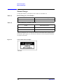
Standard:
10 cm Airline with Open
Averaging: 8
Measurement
Frequency
Power
Level
1 MHz
-3 dBm
|Z|
1 MHz
-3 dBm
θ
10 MHz
-3 dBm
|Z|
10 MHz
-3 dBm
θ
100 MHz
-3 dBm
|Z|
100 MHz
-3 dBm
θ
200 MHz
-3 dBm
|Z|
200 MHz
-3 dBm
θ
300 MHz
-3 dBm
|Z|
300 MHz
-3 dBm
θ
500 MHz
-3 dBm
|Z|
500 MHz
-3 dBm
θ
600 MHz
-3 dBm
|Z|
600 MHz
-3 dBm
θ
800 MHz
-3 dBm
|Z|
800 MHz
-3 dBm
θ
1.0 GHz
-3 dBm
|Z|
1.0 GHz
-3 dBm
θ
1.6 GHz
-3 dBm
|Z|
1.6 GHz
-3 dBm
θ
1.8 GHz
-3 dBm
|Z|
1.8 GHz
-3 dBm
θ
2.0 GHz
-3 dBm
|Z|
2.0 GHz
-3 dBm
θ
2.2 GHz
-3 dBm
|Z|
2.2 GHz
-3 dBm
θ
2.4 GHz
-3 dBm
|Z|
2.4 GHz
-3 dBm
θ
2.6 GHz
-3 dBm
|Z|
2.6 GHz
-3 dBm
θ
3.0 GHz
-3 dBm
|Z|
3.0 GHz
-3 dBm
θ
Standard:
10 cm Airline with Open
Averaging: 1
Frequency Power Level Measurement
1 MHz
1 MHz
10 MHz
10 MHz
100 MHz
100 MHz
200 MHz
-20 dBm
-20 dBm
-20 dBm
-20 dBm
-20 dBm
-20 dBm
-20 dBm
|Z|
θ
|Z|
θ
|Z|
θ
|Z|
C Copyright 2009 Agilent Technologies
○
Test Result
TAR
Ω
mrad
Ω
mrad
Ω
mrad
Ω
mrad
Ω
mrad
Ω
mrad
Ω
mrad
Ω
mrad
Ω
mrad
Ω
mrad
Ω
mrad
Ω
mrad
Ω
mrad
Ω
mrad
Ω
mrad
Ω
mrad
Measurement
Uncertainty
± 254 Ω
± 17.6 mrad
± 4.3 Ω
± 2.0 mrad
± 0.42 Ω
± 2.0 mrad
± 0.22 Ω
± 2.2 mrad
± 0.16 Ω
± 2.6 mrad
± 0.09 Ω
± 3.7 mrad
± 0.09 Ω
± 8.7 mrad
± 0.12 Ω
± 8.7 mrad
± 0.23 Ω
± 5.2 mrad
± 0.72 Ω
± 8.4 mrad
± 0.29 Ω
± 8.5 mrad
± 0.10 Ω
± 14.3 mrad
± 0.23 Ω
± 12.8 mrad
± 0.64 Ω
± 12.5 mrad
± 2.2 Ω
± 14.4 mrad
± 1.1 Ω
± 13.8 mrad
TAR
Ω
mrad
Ω
mrad
Ω
mrad
Ω
Measurement
Uncertainty
± 1771 Ω
± 50.6 mrad
± 7.7 Ω
± 5.3 mrad
± 0.42 Ω
± 2.1 mrad
± 0.22 Ω
Test Result
10.13
8.87
10.03
8.87
5.22
8.87
5.47
8.87
4.96
8.87
5.61
8.87
5.12
8.87
5.02
8.87
5.50
8.87
5.83
8.87
6.88
8.87
14.69
8.87
9.24
8.87
6.92
8.87
6.88
8.87
6.71
8.87
8.18
8.87
21.20
8.87
8.05
8.87
6.76
200 MHz
300 MHz
300 MHz
500 MHz
500 MHz
600 MHz
600 MHz
800 MHz
800 MHz
1.0 GHz
1.0 GHz
1.6 GHz
1.6 GHz
1.8 GHz
1.8 GHz
2.0 GHz
2.0 GHz
2.2 GHz
2.2 GHz
2.4 GHz
2.4 GHz
2.6 GHz
2.6 GHz
3.0 GHz
3.0 GHz
-20 dBm
-20 dBm
-20 dBm
-20 dBm
-20 dBm
-20 dBm
-20 dBm
-20 dBm
-20 dBm
-20 dBm
-20 dBm
-20 dBm
-20 dBm
-20 dBm
-20 dBm
-20 dBm
-20 dBm
-20 dBm
-20 dBm
-20 dBm
-20 dBm
-20 dBm
-20 dBm
-20 dBm
-20 dBm
θ
|Z|
θ
|Z|
θ
|Z|
θ
|Z|
θ
|Z|
θ
|Z|
θ
|Z|
θ
|Z|
θ
|Z|
θ
|Z|
θ
|Z|
θ
|Z|
θ
Standard:
10 cm Airline with Short
Averaging: 8
Frequency Power Level Measurement
1 MHz
1 MHz
10 MHz
10 MHz
100 MHz
100 MHz
200 MHz
200 MHz
300 MHz
300 MHz
500 MHz
500 MHz
600 MHz
600 MHz
1.0 GHz
1.0 GHz
1.3 GHz
1.3 GHz
1.6 GHz
-3 dBm
-3 dBm
-3 dBm
-3 dBm
-3 dBm
-3 dBm
-3 dBm
-3 dBm
-3 dBm
-3 dBm
-3 dBm
-3 dBm
-3 dBm
-3 dBm
-3 dBm
-3 dBm
-3 dBm
-3 dBm
-3 dBm
|Z|
θ
|Z|
θ
|Z|
θ
|Z|
θ
|Z|
θ
|Z|
θ
|Z|
θ
|Z|
θ
|Z|
θ
|Z|
C Copyright 2009 Agilent Technologies
○
mrad
Ω
mrad
Ω
mrad
Ω
mrad
Ω
mrad
Ω
mrad
Ω
mrad
Ω
mrad
Ω
mrad
Ω
mrad
Ω
mrad
Ω
mrad
Ω
mrad
± 2.2 mrad
± 0.16 Ω
± 2.6 mrad
± 0.09 Ω
± 3.7 mrad
± 0.09 Ω
± 8.7 mrad
± 0.12 Ω
± 8.7 mrad
± 0.23 Ω
± 5.2 mrad
± 0.72 Ω
± 8.4 mrad
± 0.29 Ω
± 8.5 mrad
± 0.10 Ω
± 14.4 mrad
± 0.23 Ω
± 12.8 mrad
± 0.64 Ω
± 12.5 mrad
± 2.2 Ω
± 14.4 mrad
± 1.1 Ω
± 13.9 mrad
Ω
mrad
Ω
mrad
Ω
mrad
Ω
mrad
Ω
mrad
Ω
mrad
Ω
mrad
Ω
mrad
Ω
mrad
Ω
Measurement
Uncertainty
± 0.002 Ω
± 19.4 mrad
± 0.005 Ω
± 4.2 mrad
± 0.03 Ω
± 2.5 mrad
± 0.07 Ω
± 3.0 mrad
± 0.11 Ω
± 3.0 mrad
± 0.31 Ω
± 3.5 mrad
± 0.77 Ω
± 5.0 mrad
± 0.45 Ω
± 5.2 mrad
± 0.19 Ω
± 8.3 mrad
± 0.12 Ω
Test Result
8.87
5.79
8.87
6.19
8.87
5.58
8.87
5.36
8.87
5.89
8.87
6.14
8.87
7.12
8.87
14.99
8.87
9.41
8.87
7.08
8.87
7.16
8.87
6.88
8.87
TAR
7.50
8.87
5.63
8.87
5.13
8.87
4.63
8.87
4.67
8.87
4.57
8.87
4.92
8.87
5.20
8.87
6.98
8.87
9.42
1.6 GHz
1.8 GHz
1.8 GHz
2.0 GHz
2.0 GHz
2.4 GHz
2.4 GHz
2.6 GHz
2.6 GHz
2.8 GHz
2.8 GHz
Standard:
Averaging:
-3 dBm
-3 dBm
-3 dBm
-3 dBm
-3 dBm
-3 dBm
-3 dBm
-3 dBm
-3 dBm
-3 dBm
-3 dBm
θ
|Z|
θ
|Z|
θ
|Z|
θ
|Z|
θ
|Z|
θ
mrad
Ω
mrad
Ω
mrad
Ω
mrad
Ω
mrad
Ω
mrad
± 10.8 mrad
± 0.31 Ω
± 8.3 mrad
± 0.91 Ω
± 10.4 mrad
± 2.06 Ω
± 13.6 mrad
± 0.74 Ω
± 13.4 mrad
± 0.30 Ω
± 13.6 mrad
Ω
mrad
Ω
mrad
Ω
mrad
Ω
mrad
Ω
mrad
Ω
mrad
Ω
mrad
Ω
mrad
Ω
mrad
Ω
mrad
Ω
mrad
Ω
mrad
Ω
mrad
Ω
mrad
Ω
mrad
Measurement
Uncertainty
± 0.010 Ω
± 68.1 mrad
± 0.011 Ω
± 8.5 mrad
± 0.03 Ω
± 2.9 mrad
± 0.07 Ω
± 3.0 mrad
± 0.12 Ω
± 3.0 mrad
± 0.31 Ω
± 3.6 mrad
± 0.80 Ω
± 5.1 mrad
± 0.45 Ω
± 5.2 mrad
± 0.19 Ω
± 8.3 mrad
± 0.12 Ω
± 11.0 mrad
± 0.31 Ω
± 8.4 mrad
± 0.92 Ω
± 10.4 mrad
± 2.06 Ω
± 13.6 mrad
± 0.74 Ω
± 13.4 mrad
± 0.30 Ω
± 13.7 mrad
8.87
6.81
8.87
7.74
8.87
7.01
8.87
6.64
8.87
8.87
8.87
10 cm Airline with Short
1
Frequency
1 MHz
1 MHz
10 MHz
10 MHz
100 MHz
100 MHz
200 MHz
200 MHz
300 MHz
300 MHz
500 MHz
500 MHz
600 MHz
600 MHz
1.0 GHz
1.0 GHz
1.3 GHz
1.3 GHz
1.6 GHz
1.6 GHz
1.8 GHz
1.8 GHz
2.0 GHz
2.0 GHz
2.4 GHz
2.4 GHz
2.6 GHz
2.6 GHz
2.8 GHz
2.8 GHz
Power Level
Measurement
-40 dBm
-40 dBm
-40 dBm
-40 dBm
-40 dBm
-40 dBm
-40 dBm
-40 dBm
-40 dBm
-40 dBm
-40 dBm
-40 dBm
-40 dBm
-40 dBm
-40 dBm
-40 dBm
-40 dBm
-40 dBm
-40 dBm
-40 dBm
-40 dBm
-40 dBm
-40 dBm
-40 dBm
-40 dBm
-40 dBm
-40 dBm
-40 dBm
-40 dBm
-40 dBm
|Z|
θ
|Z|
θ
|Z|
θ
|Z|
θ
|Z|
θ
|Z|
θ
|Z|
θ
|Z|
θ
|Z|
θ
|Z|
θ
|Z|
θ
|Z|
θ
|Z|
θ
|Z|
θ
|Z|
θ
C Copyright 2009 Agilent Technologies
○
Test Result
TAR
10.74
8.87
10.84
8.87
9.41
8.87
7.69
8.87
7.35
8.87
7.31
8.87
6.52
8.87
6.29
8.87
7.61
8.87
10.07
8.87
7.32
8.87
8.20
8.87
7.65
8.87
6.98
8.87
9.23
8.87
Change 10
Change the Measurement Uncertainty value of DC Bias Test (Option 001 & Option 010)
(Page 88) to the following information and appended TAR to this report.
DC Bias Test (Option 001 & Option 010)
Bias
Level
-40 V
-4 V
0V
4V
40 V
-50 mA
-4 mA
-100 μA
100 μA
4 mA
50 mA
Test Limit
± 46.00 mV
± 10.00 mV
± 6.00 mV
± 10.00 mV
± 46.00 mV
± 120.0 μA
± 28.0 μA
± 20.2 μA
± 20.2 μA
± 28.0 μA
± 120.0 μA
C Copyright 2009 Agilent Technologies
○
Test Result
mV
μV
μV
μV
mV
μA
μA
μA
μA
μA
μA
±
±
±
±
±
±
±
±
±
±
±
Measurement
Uncertainty
TAR
0.87 mV
68.5 μV
13.3 μV
45.5 μV
0.88 mV
8.9 μA
1.2 μA
1.0 μA
1.2 μA
1.3 μA
8.9 μA
52.90
146.00
454.70
220.10
52.80
13.51
25.34
21.67
17.86
22.42
13.57
Agilent E4991A RF Impedance/Material Analyzer
Service Manual
Fifth Edition
Manufacturing No. E4991 - 90140
September 2008
Notices
The information contained in this document is subject to change without notice.
This document contains proprietary information that is protected by copyright. All rights
are reserved. No part of this document may be photocopied, reproduced, or translated to
another language without the prior written consent of Agilent Technologies.
Microsoft ,MS-DOS ,Windows ,Visual C++ ,Visual Basic ,VBA
registered
and Excel
are
UNIX is a registered trademark in U.S. and other countries, licensed
exclusively through X/Open Company Limited.
Portions
Copyright 1996, Microsoft Corporation. All rights reserved.
Copyright 2001, 2003, 2004, 2005, 2008 Agilent Technologies
Manual Printing History
The manual’s printing date and part number indicate its current edition. The printing date
changes when a new edition is printed. (Minor corrections and updates that are
incorporated at reprint do not cause the date to change.) The manual part number changes
when extensive technical changes are incorporated.
December 2001
First Edition
April 2003
Second Edition
November 2004
Third Edition
December 2005
Fourth Edition
September 2008
Fifth Edition (E4991 - 90140)
2
Safety Summary
The following general safety precautions must be observed during all phases of operation,
service, and repair of this instrument. Failure to comply with these precautions or with
specific WARNINGS elsewhere in this manual may impair the protection provided by the
equipment. In addition it violates safety standards of design, manufacture, and intended use
of the instrument.
Agilent Technologies assumes no liability for the customer’s failure to comply with these
requirements.
NOTE
The E4991A complies with INSTALLATION CATEGORY II as well as POLLUTION
DEGREE 2 in IEC61010-1. The E4991A is an INDOOR USE product.
NOTE
The LEDs in the E4991A are Class 1 in accordance with IEC60825-1,
CLASS 1 LED PRODUCT
NOTE
This equipment is MEASUREMENT CATEGORY I (CAT I). Do not use for CAT II, III,
or IV.
NOTE
This equipment is tested with stand-alone condition or with the combination with the
accessories supplied by Agilent Technologies against the requirement of the standards
described in the Declaration of Conformity. If it is used as a system component,
compliance of related regulations and safety requirements are to be confirmed by the
builder of the system.
•
Ground the Instrument
To avoid electric shock, the instrument chassis and cabinet must be grounded with the
supplied power cable’s grounding prong.
•
DO NOT Operate in an Explosive Atmosphere
Do not operate the instrument in the presence of inflammable gasses or fumes.
Operation of any electrical instrument in such an environment clearly constitutes a
safety hazard.
•
Keep Away from Live Circuits
Operators must not remove instrument covers. Component replacement and internal
adjustments must be made by qualified maintenance personnel. Do not replace
components with the power cable connected. Under certain conditions, dangerous
voltage levels may remain even after the power cable has been disconnected. To avoid
injuries, always disconnect the power and discharge circuits before touching them.
•
DO NOT Service or Adjust the Instrument Alone
Do not attempt internal service or adjustment unless another person, capable of
rendering first aid and resuscitation, is present.
•
DO NOT Substitute Parts or Modify the Instrument
To avoid the danger of introducing additional hazards, do not install substitute parts or
perform unauthorized modifications to the instrument. Return the instrument to an
3
Agilent Technologies Sales and Service Office for service and repair to ensure that
safety features are maintained in operational condition.
•
Dangerous Procedure Warnings
Warnings, such as the example below, precede potentially dangerous procedures
throughout this manual. Instructions contained in the warnings must be followed.
WARNING
Dangerous voltage levels, capable of causing death, are present in this instrument.
Use extreme caution when handling, testing, and adjusting this instrument.
•
Do not connect the measuring terminals to mains.
Safety Symbol
General definitions of safety symbols used on the instrument or in manuals are listed
below.
Instruction Manual symbol: the product is marked with this symbol when it is necessary for
the user to refer to the instrument manual.
Alternating current.
Direct current.
On (Supply).
Off (Supply).
In position of push-button switch.
Out position of push-button switch.
Frame (or chassis) terminal. A connection to the frame (chassis) of the equipment which
normally include all exposed metal structure.
WARNING
This warning sign denotes a hazard. It calls attention to a procedure, practice,
condition or the like, which, if not correctly performed or adhered to, could result in
injury or death to personnel.
CAUTION
This Caution sign denotes a hazard. It calls attention to a procedure, practice, condition or
the like, which, if not correctly performed or adhered to, could result in damage to or
destruction of part or all of the product.
NOTE
Note denotes important information. It calls attention to a procedure, practice, condition or
the like, which is essential to highlight.
4
Certification
Agilent Technologies certifies that this product met its published specifications at the time
of shipment from the factory. Agilent Technologies further certifies that its calibration
measurements are traceable to the United States National Institute of Standards and
Technology, to the extent allowed by the Institution’s calibration facility, or to the
calibration facilities of other International Standards Organization members.
Documentation Warranty
The material contained in this document is provided "as is," and is subject to being
changed, without notice, in future editions. Further, to the maximum extent permitted by
applicable law, Agilent disclaims all warranties, either express or implied with regard to
this manual and any information contained herein, including but not limited to the implied
warranties of merchantability and fitness for a particular purpose. Agilent shall not be
liable for errors or for incidental or consequential damages in connection with the
furnishing, use, or performance of this document or any information contained herein.
Should Agilent and the user have a separate written agreement with warranty terms
covering the material in this document that conflict with these terms, the warranty terms in
the separate agreement will control.
Exclusive Remedies
The remedies provided herein are buyer’s sole and exclusive remedies. Agilent
Technologies shall not be liable for any direct, indirect, special, incidental, or
consequential damages, whether based on contract, tort, or any other legal theory.
Assistance
Product maintenance agreements and other customer assistance agreements are available
for Agilent Technologies products.
For any assistance, contact your nearest Agilent Technologies Sales and Service Office.
Addresses are provided at the back of this manual.
5
Typeface Conventions
Bold
Boldface type is used when a term is defined. For
example: icons are symbols.
Italic
Italic type is used for emphasis and for titles of
manuals and other publications.
[Hardkey]
Indicates a hardkey labeled “Hardkey.”
Softkey
Indicates a softkey labeled “Softkey.”
[Hardkey] - Softkey1 - Softkey2
Indicates keystrokes [Hardkey] - Softkey1 Softkey2.
E4991A Documentation Map
The following manuals are available for the E4991A.
•
Operation Manual (P/N: E4991-900x0)
Most of basic information necessary for using E4991A is described in this manual. It
includes the way of installation, preparation, measurement operation including
calibration, performances (specifications), key definitions, and error messages.
•
Programming Manual (P/N: E4991-900x1)
The Programming Manual shows how to write and use program to control the E4991A.
•
Service Manual (P/N: E4991-901x0)
This manual describes how to adjust and repair the E4991A, and how to carry out
performance tests.
Microsoft , MS-DOS , Windows , and Visual Basic for Applications are registered
trademarks of Microsoft Corporation in U.S. and other countries.
6
Software Installed
The Windows operating system installed in this machine is customized for more effective
operation, and has different functions that are not part of the Windows operating system for
ordinary PCs (personal computers). Therefore, do not attempt to use the system in ways
other than those described in this manual or to install Windows-based software (including
anti-virus software) for ordinary PCs as doing so may cause malfunctions.
Also note the followings.
•
Do not update the Windows operating system installed in this machine to the Windows
operating system for ordinary PCs. Doing so will cause malfunctions.
•
Do not allow any computer virus to infect the system. This machine has no virus check
function nor anti-virus software installed.
Agilent Technologies will not be held liable for any failure or damage arising from
negligence regarding these prohibitions and warnings.
NOTE
If the pre-installed software is damaged somehow, resulting in errant behavior by the
machine, perform a "system recovery".
7
8
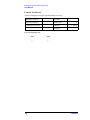
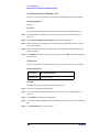
Contents
1. General Information
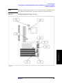
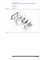
Organization of Service Manual . . . . . . . . . . . . . . . . . . . . . . . . . . . . . . . . . . . . . . . . . . . . . . . . . . . . . . . . . . 18
Instrument Covered by This Manual . . . . . . . . . . . . . . . . . . . . . . . . . . . . . . . . . . . . . . . . . . . . . . . . . . . . . . 20
Required Equipment . . . . . . . . . . . . . . . . . . . . . . . . . . . . . . . . . . . . . . . . . . . . . . . . . . . . . . . . . . . . . . . . . . . 21
2. Performance Test and Function Test
Required Equipment . . . . . . . . . . . . . . . . . . . . . . . . . . . . . . . . . . . . . . . . . . . . . . . . . . . . . . . . . . . . . . . . . . . 24
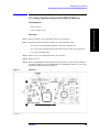
How to Set the E4991A for Maintenance . . . . . . . . . . . . . . . . . . . . . . . . . . . . . . . . . . . . . . . . . . . . . . . . . . . 25
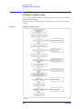
Performance Test . . . . . . . . . . . . . . . . . . . . . . . . . . . . . . . . . . . . . . . . . . . . . . . . . . . . . . . . . . . . . . . . . . . . . 27
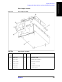
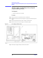
Introduction . . . . . . . . . . . . . . . . . . . . . . . . . . . . . . . . . . . . . . . . . . . . . . . . . . . . . . . . . . . . . . . . . . . . . . . . 27
Frequency Accuracy Test . . . . . . . . . . . . . . . . . . . . . . . . . . . . . . . . . . . . . . . . . . . . . . . . . . . . . . . . . . . . . 28
Power Level Accuracy Test. . . . . . . . . . . . . . . . . . . . . . . . . . . . . . . . . . . . . . . . . . . . . . . . . . . . . . . . . . . . 31
Impedance Measurement Accuracy Test. . . . . . . . . . . . . . . . . . . . . . . . . . . . . . . . . . . . . . . . . . . . . . . . . . 35
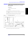
DC Bias Level Accuracy Test (Option 001) . . . . . . . . . . . . . . . . . . . . . . . . . . . . . . . . . . . . . . . . . . . . . . . 42
Performance Test (for Option 007 Temperature Characteristic Test Kit) . . . . . . . . . . . . . . . . . . . . . . . . . . . 46
Introduction . . . . . . . . . . . . . . . . . . . . . . . . . . . . . . . . . . . . . . . . . . . . . . . . . . . . . . . . . . . . . . . . . . . . . . . . 46
Required Test. . . . . . . . . . . . . . . . . . . . . . . . . . . . . . . . . . . . . . . . . . . . . . . . . . . . . . . . . . . . . . . . . . . . . . . 46
Specification . . . . . . . . . . . . . . . . . . . . . . . . . . . . . . . . . . . . . . . . . . . . . . . . . . . . . . . . . . . . . . . . . . . . . . . 46
Required Equipment . . . . . . . . . . . . . . . . . . . . . . . . . . . . . . . . . . . . . . . . . . . . . . . . . . . . . . . . . . . . . . . . . 46
Test Procedure . . . . . . . . . . . . . . . . . . . . . . . . . . . . . . . . . . . . . . . . . . . . . . . . . . . . . . . . . . . . . . . . . . . . . . 46
Performance Test (for Option 010 Probe Station Connection Kit). . . . . . . . . . . . . . . . . . . . . . . . . . . . . . . . 48
Introduction . . . . . . . . . . . . . . . . . . . . . . . . . . . . . . . . . . . . . . . . . . . . . . . . . . . . . . . . . . . . . . . . . . . . . . . . 48
Required Test. . . . . . . . . . . . . . . . . . . . . . . . . . . . . . . . . . . . . . . . . . . . . . . . . . . . . . . . . . . . . . . . . . . . . . . 48
Specification . . . . . . . . . . . . . . . . . . . . . . . . . . . . . . . . . . . . . . . . . . . . . . . . . . . . . . . . . . . . . . . . . . . . . . . 48
Test Procedure . . . . . . . . . . . . . . . . . . . . . . . . . . . . . . . . . . . . . . . . . . . . . . . . . . . . . . . . . . . . . . . . . . . . . . 49
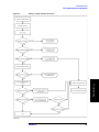
Function Test. . . . . . . . . . . . . . . . . . . . . . . . . . . . . . . . . . . . . . . . . . . . . . . . . . . . . . . . . . . . . . . . . . . . . . . . . 51
Introduction . . . . . . . . . . . . . . . . . . . . . . . . . . . . . . . . . . . . . . . . . . . . . . . . . . . . . . . . . . . . . . . . . . . . . . . . 51
Warm Up Time . . . . . . . . . . . . . . . . . . . . . . . . . . . . . . . . . . . . . . . . . . . . . . . . . . . . . . . . . . . . . . . . . . . . . 51
Ambient Conditions . . . . . . . . . . . . . . . . . . . . . . . . . . . . . . . . . . . . . . . . . . . . . . . . . . . . . . . . . . . . . . . . . 51
Low Loss Capacitor Check . . . . . . . . . . . . . . . . . . . . . . . . . . . . . . . . . . . . . . . . . . . . . . . . . . . . . . . . . . . . 52
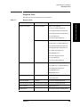
Calculating Sheet . . . . . . . . . . . . . . . . . . . . . . . . . . . . . . . . . . . . . . . . . . . . . . . . . . . . . . . . . . . . . . . . . . . . . 53
Performance Test. . . . . . . . . . . . . . . . . . . . . . . . . . . . . . . . . . . . . . . . . . . . . . . . . . . . . . . . . . . . . . . . . . . . 53
Function Test . . . . . . . . . . . . . . . . . . . . . . . . . . . . . . . . . . . . . . . . . . . . . . . . . . . . . . . . . . . . . . . . . . . . . . . 73
Test Record . . . . . . . . . . . . . . . . . . . . . . . . . . . . . . . . . . . . . . . . . . . . . . . . . . . . . . . . . . . . . . . . . . . . . . . . . . 74
Performance Test Record . . . . . . . . . . . . . . . . . . . . . . . . . . . . . . . . . . . . . . . . . . . . . . . . . . . . . . . . . . . . . 74
Performance Test Record (Option 007). . . . . . . . . . . . . . . . . . . . . . . . . . . . . . . . . . . . . . . . . . . . . . . . . . . 89
Performance Test Record (Option 010). . . . . . . . . . . . . . . . . . . . . . . . . . . . . . . . . . . . . . . . . . . . . . . . . . 102
Function Test Record . . . . . . . . . . . . . . . . . . . . . . . . . . . . . . . . . . . . . . . . . . . . . . . . . . . . . . . . . . . . . . . 116
3. Adjustment
Safety Considerations . . . . . . . . . . . . . . . . . . . . . . . . . . . . . . . . . . . . . . . . . . . . . . . . . . . . . . . . . . . . . . . . .
Warm-up for Adjustment . . . . . . . . . . . . . . . . . . . . . . . . . . . . . . . . . . . . . . . . . . . . . . . . . . . . . . . . . . . . . .
Required Equipment . . . . . . . . . . . . . . . . . . . . . . . . . . . . . . . . . . . . . . . . . . . . . . . . . . . . . . . . . . . . . . . . . .
Preparation for using the Adjustment Program . . . . . . . . . . . . . . . . . . . . . . . . . . . . . . . . . . . . . . . . . . . . .
Required Controller. . . . . . . . . . . . . . . . . . . . . . . . . . . . . . . . . . . . . . . . . . . . . . . . . . . . . . . . . . . . . . . . .
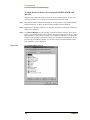
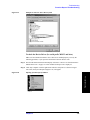
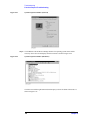
Installing a GPIB Card (82340B, 82341C/D or 82350A). . . . . . . . . . . . . . . . . . . . . . . . . . . . . . . . . . . .
Installing Agilent VEE for Personal Computer. . . . . . . . . . . . . . . . . . . . . . . . . . . . . . . . . . . . . . . . . . . .
Installing Adjustment Program into Your PC . . . . . . . . . . . . . . . . . . . . . . . . . . . . . . . . . . . . . . . . . . . .
118
118
118
119
119
119
119
119
9
Contents
Equipment Setup . . . . . . . . . . . . . . . . . . . . . . . . . . . . . . . . . . . . . . . . . . . . . . . . . . . . . . . . . . . . . . . . . .
E4991A Control Mode. . . . . . . . . . . . . . . . . . . . . . . . . . . . . . . . . . . . . . . . . . . . . . . . . . . . . . . . . . . . . .
Order of Adjustment. . . . . . . . . . . . . . . . . . . . . . . . . . . . . . . . . . . . . . . . . . . . . . . . . . . . . . . . . . . . . . . . . .
Required Adjustment after Replacing Assembly . . . . . . . . . . . . . . . . . . . . . . . . . . . . . . . . . . . . . . . . . . . .
Adjustment Program. . . . . . . . . . . . . . . . . . . . . . . . . . . . . . . . . . . . . . . . . . . . . . . . . . . . . . . . . . . . . . . . . .
Adjustment Program Menu. . . . . . . . . . . . . . . . . . . . . . . . . . . . . . . . . . . . . . . . . . . . . . . . . . . . . . . . . . .
How to perform the Adjustment Program . . . . . . . . . . . . . . . . . . . . . . . . . . . . . . . . . . . . . . . . . . . . . . .
Initialization of the System Calibration Data . . . . . . . . . . . . . . . . . . . . . . . . . . . . . . . . . . . . . . . . . . . . . . .
Required Equipment . . . . . . . . . . . . . . . . . . . . . . . . . . . . . . . . . . . . . . . . . . . . . . . . . . . . . . . . . . . . . . . .
Procedure . . . . . . . . . . . . . . . . . . . . . . . . . . . . . . . . . . . . . . . . . . . . . . . . . . . . . . . . . . . . . . . . . . . . . . . .
A1 VCXO Frequency Adjustment . . . . . . . . . . . . . . . . . . . . . . . . . . . . . . . . . . . . . . . . . . . . . . . . . . . . . . .
Required Equipment . . . . . . . . . . . . . . . . . . . . . . . . . . . . . . . . . . . . . . . . . . . . . . . . . . . . . . . . . . . . . . . .
Procedure . . . . . . . . . . . . . . . . . . . . . . . . . . . . . . . . . . . . . . . . . . . . . . . . . . . . . . . . . . . . . . . . . . . . . . . .
A3 Local Level Adjustment . . . . . . . . . . . . . . . . . . . . . . . . . . . . . . . . . . . . . . . . . . . . . . . . . . . . . . . . . . . .
Required Equipment . . . . . . . . . . . . . . . . . . . . . . . . . . . . . . . . . . . . . . . . . . . . . . . . . . . . . . . . . . . . . . . .
Procedure . . . . . . . . . . . . . . . . . . . . . . . . . . . . . . . . . . . . . . . . . . . . . . . . . . . . . . . . . . . . . . . . . . . . . . . .
A3 Output AGC Gain Adjustment . . . . . . . . . . . . . . . . . . . . . . . . . . . . . . . . . . . . . . . . . . . . . . . . . . . . . . .
Required Equipment . . . . . . . . . . . . . . . . . . . . . . . . . . . . . . . . . . . . . . . . . . . . . . . . . . . . . . . . . . . . . . . .
Procedure . . . . . . . . . . . . . . . . . . . . . . . . . . . . . . . . . . . . . . . . . . . . . . . . . . . . . . . . . . . . . . . . . . . . . . . .
A3 Output Level Adjustment . . . . . . . . . . . . . . . . . . . . . . . . . . . . . . . . . . . . . . . . . . . . . . . . . . . . . . . . . . .
Required Equipment . . . . . . . . . . . . . . . . . . . . . . . . . . . . . . . . . . . . . . . . . . . . . . . . . . . . . . . . . . . . . . . .
Procedure . . . . . . . . . . . . . . . . . . . . . . . . . . . . . . . . . . . . . . . . . . . . . . . . . . . . . . . . . . . . . . . . . . . . . . . .
A4 AGC Gain Adjustment . . . . . . . . . . . . . . . . . . . . . . . . . . . . . . . . . . . . . . . . . . . . . . . . . . . . . . . . . . . . .
Required Equipment . . . . . . . . . . . . . . . . . . . . . . . . . . . . . . . . . . . . . . . . . . . . . . . . . . . . . . . . . . . . . . . .
Procedure . . . . . . . . . . . . . . . . . . . . . . . . . . . . . . . . . . . . . . . . . . . . . . . . . . . . . . . . . . . . . . . . . . . . . . . .
A4 Local Level Adjustment . . . . . . . . . . . . . . . . . . . . . . . . . . . . . . . . . . . . . . . . . . . . . . . . . . . . . . . . . . . .
Required Equipment . . . . . . . . . . . . . . . . . . . . . . . . . . . . . . . . . . . . . . . . . . . . . . . . . . . . . . . . . . . . . . . .
Procedure . . . . . . . . . . . . . . . . . . . . . . . . . . . . . . . . . . . . . . . . . . . . . . . . . . . . . . . . . . . . . . . . . . . . . . . .
A4 IF Gain Adjustment . . . . . . . . . . . . . . . . . . . . . . . . . . . . . . . . . . . . . . . . . . . . . . . . . . . . . . . . . . . . . . .
Required Equipment . . . . . . . . . . . . . . . . . . . . . . . . . . . . . . . . . . . . . . . . . . . . . . . . . . . . . . . . . . . . . . . .
Procedure . . . . . . . . . . . . . . . . . . . . . . . . . . . . . . . . . . . . . . . . . . . . . . . . . . . . . . . . . . . . . . . . . . . . . . . .
Default Cal Coefficient Adjustment . . . . . . . . . . . . . . . . . . . . . . . . . . . . . . . . . . . . . . . . . . . . . . . . . . . . . .
Required Equipment . . . . . . . . . . . . . . . . . . . . . . . . . . . . . . . . . . . . . . . . . . . . . . . . . . . . . . . . . . . . . . . .
Procedure . . . . . . . . . . . . . . . . . . . . . . . . . . . . . . . . . . . . . . . . . . . . . . . . . . . . . . . . . . . . . . . . . . . . . . . .
A5 Reference Oven Adjustment (Opt 1D5 only) . . . . . . . . . . . . . . . . . . . . . . . . . . . . . . . . . . . . . . . . . . . .
Required Equipment . . . . . . . . . . . . . . . . . . . . . . . . . . . . . . . . . . . . . . . . . . . . . . . . . . . . . . . . . . . . . . . .
Procedure . . . . . . . . . . . . . . . . . . . . . . . . . . . . . . . . . . . . . . . . . . . . . . . . . . . . . . . . . . . . . . . . . . . . . . . .
A2 DC Bias Voltage Adjustment (Opt 001 only) . . . . . . . . . . . . . . . . . . . . . . . . . . . . . . . . . . . . . . . . . . . .
Required Equipment . . . . . . . . . . . . . . . . . . . . . . . . . . . . . . . . . . . . . . . . . . . . . . . . . . . . . . . . . . . . . . . .
Procedure . . . . . . . . . . . . . . . . . . . . . . . . . . . . . . . . . . . . . . . . . . . . . . . . . . . . . . . . . . . . . . . . . . . . . . . .
A2 DC Bias Current Adjustment (Opt 001 only). . . . . . . . . . . . . . . . . . . . . . . . . . . . . . . . . . . . . . . . . . . .
Required Equipment . . . . . . . . . . . . . . . . . . . . . . . . . . . . . . . . . . . . . . . . . . . . . . . . . . . . . . . . . . . . . . . .
Procedure . . . . . . . . . . . . . . . . . . . . . . . . . . . . . . . . . . . . . . . . . . . . . . . . . . . . . . . . . . . . . . . . . . . . . . . .
A2 DC Bias Output Resistor/Conductance Adjustment (Opt 001 only) . . . . . . . . . . . . . . . . . . . . . . . . . .
Required Equipment . . . . . . . . . . . . . . . . . . . . . . . . . . . . . . . . . . . . . . . . . . . . . . . . . . . . . . . . . . . . . . . .
Procedure . . . . . . . . . . . . . . . . . . . . . . . . . . . . . . . . . . . . . . . . . . . . . . . . . . . . . . . . . . . . . . . . . . . . . . . .
Writing the Instrument ID . . . . . . . . . . . . . . . . . . . . . . . . . . . . . . . . . . . . . . . . . . . . . . . . . . . . . . . . . . . . .
Required Equipment . . . . . . . . . . . . . . . . . . . . . . . . . . . . . . . . . . . . . . . . . . . . . . . . . . . . . . . . . . . . . . . .
Procedure . . . . . . . . . . . . . . . . . . . . . . . . . . . . . . . . . . . . . . . . . . . . . . . . . . . . . . . . . . . . . . . . . . . . . . . .
10
120
121
122
124
125
125
128
132
132
132
133
133
133
134
134
134
135
135
135
136
136
136
138
138
138
139
139
139
140
140
140
141
141
141
142
142
142
144
144
144
145
145
145
146
146
146
148
148
148
Contents
How to confirm the E4991A option installed . . . . . . . . . . . . . . . . . . . . . . . . . . . . . . . . . . . . . . . . . . . . 148
System Backup (for serial prefix JP1KH, JP2KH, and MY432) . . . . . . . . . . . . . . . . . . . . . . . . . . . . . . . . 149
How to make a system backup disk . . . . . . . . . . . . . . . . . . . . . . . . . . . . . . . . . . . . . . . . . . . . . . . . . . . . 149
System backup Procedure . . . . . . . . . . . . . . . . . . . . . . . . . . . . . . . . . . . . . . . . . . . . . . . . . . . . . . . . . . . 149
4. Troubleshooting
Introduction. . . . . . . . . . . . . . . . . . . . . . . . . . . . . . . . . . . . . . . . . . . . . . . . . . . . . . . . . . . . . . . . . . . . . . . . . 154
How to exit from the E4991A Measurement View . . . . . . . . . . . . . . . . . . . . . . . . . . . . . . . . . . . . . . . . . . 155
To Troubleshoot the Instrument . . . . . . . . . . . . . . . . . . . . . . . . . . . . . . . . . . . . . . . . . . . . . . . . . . . . . . . . . 156
Primary Trouble Isolation . . . . . . . . . . . . . . . . . . . . . . . . . . . . . . . . . . . . . . . . . . . . . . . . . . . . . . . . . . . . 156
No Display Troubleshooting. . . . . . . . . . . . . . . . . . . . . . . . . . . . . . . . . . . . . . . . . . . . . . . . . . . . . . . . . . . . 158
Booting Process Troubleshooting (for serial prefix JP1KH, JP2KH, and MY432) . . . . . . . . . . . . . . . . . . 161
Booting Process Troubleshooting (for serial prefix MY433 and later) . . . . . . . . . . . . . . . . . . . . . . . . . . . 168
Troubleshooting Using Internal Test. . . . . . . . . . . . . . . . . . . . . . . . . . . . . . . . . . . . . . . . . . . . . . . . . . . . . . 172
Power On Self Test . . . . . . . . . . . . . . . . . . . . . . . . . . . . . . . . . . . . . . . . . . . . . . . . . . . . . . . . . . . . . . . . . 172
PLL unlock . . . . . . . . . . . . . . . . . . . . . . . . . . . . . . . . . . . . . . . . . . . . . . . . . . . . . . . . . . . . . . . . . . . . . . . 172
To Execute the Internal Test . . . . . . . . . . . . . . . . . . . . . . . . . . . . . . . . . . . . . . . . . . . . . . . . . . . . . . . . . . 172
Internal Test. . . . . . . . . . . . . . . . . . . . . . . . . . . . . . . . . . . . . . . . . . . . . . . . . . . . . . . . . . . . . . . . . . . . . . . 172
Analog Test Failure Troubleshooting in the Internal Test. . . . . . . . . . . . . . . . . . . . . . . . . . . . . . . . . . . . 173
System Test Failure Troubleshooting in the Internal Test. . . . . . . . . . . . . . . . . . . . . . . . . . . . . . . . . . . . 174
Function Depend Troubleshooting . . . . . . . . . . . . . . . . . . . . . . . . . . . . . . . . . . . . . . . . . . . . . . . . . . . . . . . 175
Functions . . . . . . . . . . . . . . . . . . . . . . . . . . . . . . . . . . . . . . . . . . . . . . . . . . . . . . . . . . . . . . . . . . . . . . . . . 175
To check the Front Panel . . . . . . . . . . . . . . . . . . . . . . . . . . . . . . . . . . . . . . . . . . . . . . . . . . . . . . . . . . . . . 179
To check the LCD . . . . . . . . . . . . . . . . . . . . . . . . . . . . . . . . . . . . . . . . . . . . . . . . . . . . . . . . . . . . . . . . . . 179
To check the External Keyboard . . . . . . . . . . . . . . . . . . . . . . . . . . . . . . . . . . . . . . . . . . . . . . . . . . . . . . . 179
To check the Mouse. . . . . . . . . . . . . . . . . . . . . . . . . . . . . . . . . . . . . . . . . . . . . . . . . . . . . . . . . . . . . . . . . 180
To check the FDD . . . . . . . . . . . . . . . . . . . . . . . . . . . . . . . . . . . . . . . . . . . . . . . . . . . . . . . . . . . . . . . . . . 180
To check the VGA Display Output . . . . . . . . . . . . . . . . . . . . . . . . . . . . . . . . . . . . . . . . . . . . . . . . . . . . . 180
To check the External Trigger Input . . . . . . . . . . . . . . . . . . . . . . . . . . . . . . . . . . . . . . . . . . . . . . . . . . . . 181
To check the LAN (for serial prefix JP1KH, JP2KH, and MY432) . . . . . . . . . . . . . . . . . . . . . . . . . . . . 181
To Check the LAN (for serial prefix MY433 and later) . . . . . . . . . . . . . . . . . . . . . . . . . . . . . . . . . . . . . 184
To check the Printer Parallel port ( for serial prefix JP1KH, JP2KH, and MY432) . . . . . . . . . . . . . . . . 188
To check the Printer USB port ( for serial prefix MY433 and later). . . . . . . . . . . . . . . . . . . . . . . . . . . . 188
To check the GPIB . . . . . . . . . . . . . . . . . . . . . . . . . . . . . . . . . . . . . . . . . . . . . . . . . . . . . . . . . . . . . . . . . 188
External Tests Failure Troubleshooting . . . . . . . . . . . . . . . . . . . . . . . . . . . . . . . . . . . . . . . . . . . . . . . . . . . 189
To Execute the External Test. . . . . . . . . . . . . . . . . . . . . . . . . . . . . . . . . . . . . . . . . . . . . . . . . . . . . . . . . . 189
The contents of the external test . . . . . . . . . . . . . . . . . . . . . . . . . . . . . . . . . . . . . . . . . . . . . . . . . . . . . . . 189
Front Keyboard & LCD Display Test . . . . . . . . . . . . . . . . . . . . . . . . . . . . . . . . . . . . . . . . . . . . . . . . . . . 190
Source Test . . . . . . . . . . . . . . . . . . . . . . . . . . . . . . . . . . . . . . . . . . . . . . . . . . . . . . . . . . . . . . . . . . . . . . . 190
Out ATT Test . . . . . . . . . . . . . . . . . . . . . . . . . . . . . . . . . . . . . . . . . . . . . . . . . . . . . . . . . . . . . . . . . . . . . . 191
Input ATT Test . . . . . . . . . . . . . . . . . . . . . . . . . . . . . . . . . . . . . . . . . . . . . . . . . . . . . . . . . . . . . . . . . . . . 191
IF Gain Test . . . . . . . . . . . . . . . . . . . . . . . . . . . . . . . . . . . . . . . . . . . . . . . . . . . . . . . . . . . . . . . . . . . . . . . 192
Front Isolation Test . . . . . . . . . . . . . . . . . . . . . . . . . . . . . . . . . . . . . . . . . . . . . . . . . . . . . . . . . . . . . . . . . 192
Test Head Test . . . . . . . . . . . . . . . . . . . . . . . . . . . . . . . . . . . . . . . . . . . . . . . . . . . . . . . . . . . . . . . . . . . . . 193
DC Bias Test (Option 001 only) . . . . . . . . . . . . . . . . . . . . . . . . . . . . . . . . . . . . . . . . . . . . . . . . . . . . . . . 193
Z Meas Test . . . . . . . . . . . . . . . . . . . . . . . . . . . . . . . . . . . . . . . . . . . . . . . . . . . . . . . . . . . . . . . . . . . . . . . 194
External Test Failure Troubleshooting . . . . . . . . . . . . . . . . . . . . . . . . . . . . . . . . . . . . . . . . . . . . . . . . . . 195
Performance Tests Failure Troubleshooting . . . . . . . . . . . . . . . . . . . . . . . . . . . . . . . . . . . . . . . . . . . . . . . . 196
Troubleshooting for Performance Test Failure . . . . . . . . . . . . . . . . . . . . . . . . . . . . . . . . . . . . . . . . . . . . 196
11
Contents
To Configure the A20 Digital Motherboard and BIOS (for serial prefix JP1KH, JP2KH, and MY432) .
To Identify the Motherboard Used . . . . . . . . . . . . . . . . . . . . . . . . . . . . . . . . . . . . . . . . . . . . . . . . . . . . .
Configure the Motherboard . . . . . . . . . . . . . . . . . . . . . . . . . . . . . . . . . . . . . . . . . . . . . . . . . . . . . . . . . .
To Confirm or Set the BIOS Options . . . . . . . . . . . . . . . . . . . . . . . . . . . . . . . . . . . . . . . . . . . . . . . . . . .
To Configure the A20 Digital Motherboard and BIOS (for serial prefix MY433 and later) . . . . . . . . . . .
To Identify the Motherboard Installed . . . . . . . . . . . . . . . . . . . . . . . . . . . . . . . . . . . . . . . . . . . . . . . . . .
Configure the Motherboard . . . . . . . . . . . . . . . . . . . . . . . . . . . . . . . . . . . . . . . . . . . . . . . . . . . . . . . . . .
Testing DRAM on the Motherboard . . . . . . . . . . . . . . . . . . . . . . . . . . . . . . . . . . . . . . . . . . . . . . . . . . . .
To Confirm or Set the BIOS Options . . . . . . . . . . . . . . . . . . . . . . . . . . . . . . . . . . . . . . . . . . . . . . . . . . .
197
197
198
200
210
210
210
210
211
5. Theory of Operation
Overall Instrument Operation. . . . . . . . . . . . . . . . . . . . . . . . . . . . . . . . . . . . . . . . . . . . . . . . . . . . . . . . . . .
Digital Section . . . . . . . . . . . . . . . . . . . . . . . . . . . . . . . . . . . . . . . . . . . . . . . . . . . . . . . . . . . . . . . . . . . . . .
A20 Digital Motherboard (for serial prefix JP1KH, JP2KH, and MY432) . . . . . . . . . . . . . . . . . . . . . .
A20 Digital Motherboard (for serial prefix MY433 and later). . . . . . . . . . . . . . . . . . . . . . . . . . . . . . . .
A21 Analog Interface Board. . . . . . . . . . . . . . . . . . . . . . . . . . . . . . . . . . . . . . . . . . . . . . . . . . . . . . . . . .
A22 Front Panel Keyboard . . . . . . . . . . . . . . . . . . . . . . . . . . . . . . . . . . . . . . . . . . . . . . . . . . . . . . . . . . .
A24 GPIB Board. . . . . . . . . . . . . . . . . . . . . . . . . . . . . . . . . . . . . . . . . . . . . . . . . . . . . . . . . . . . . . . . . . .
A25 LAN Interface Board (for serial prefix JP1KH, JP2KH, and MY432). . . . . . . . . . . . . . . . . . . . . .
A26 Display Board . . . . . . . . . . . . . . . . . . . . . . . . . . . . . . . . . . . . . . . . . . . . . . . . . . . . . . . . . . . . . . . . .
A27 Mass Storage Disk Drive . . . . . . . . . . . . . . . . . . . . . . . . . . . . . . . . . . . . . . . . . . . . . . . . . . . . . . . .
A28 FDD (Floppy Disk Drive) . . . . . . . . . . . . . . . . . . . . . . . . . . . . . . . . . . . . . . . . . . . . . . . . . . . . . . .
A51 LCD (Liquid Crystal Display) . . . . . . . . . . . . . . . . . . . . . . . . . . . . . . . . . . . . . . . . . . . . . . . . . . . .
A52 Inverter Board . . . . . . . . . . . . . . . . . . . . . . . . . . . . . . . . . . . . . . . . . . . . . . . . . . . . . . . . . . . . . . . . .
Analog Section . . . . . . . . . . . . . . . . . . . . . . . . . . . . . . . . . . . . . . . . . . . . . . . . . . . . . . . . . . . . . . . . . . . . . .
A1 Reference Oscillator Board. . . . . . . . . . . . . . . . . . . . . . . . . . . . . . . . . . . . . . . . . . . . . . . . . . . . . . . .
A3 Source Board. . . . . . . . . . . . . . . . . . . . . . . . . . . . . . . . . . . . . . . . . . . . . . . . . . . . . . . . . . . . . . . . . . .
A4 Receiver Board . . . . . . . . . . . . . . . . . . . . . . . . . . . . . . . . . . . . . . . . . . . . . . . . . . . . . . . . . . . . . . . . .
A6 Test Head Board(for the standard and Option 010) . . . . . . . . . . . . . . . . . . . . . . . . . . . . . . . . . . . . .
A10 Analog Motherboard . . . . . . . . . . . . . . . . . . . . . . . . . . . . . . . . . . . . . . . . . . . . . . . . . . . . . . . . . . . .
A2 DC Bias Board (Option 001) . . . . . . . . . . . . . . . . . . . . . . . . . . . . . . . . . . . . . . . . . . . . . . . . . . . . . .
A5 Reference Oven Board (Option 1D5) . . . . . . . . . . . . . . . . . . . . . . . . . . . . . . . . . . . . . . . . . . . . . . . .
220
223
223
223
223
223
223
223
223
224
224
224
224
225
227
227
228
229
229
229
229
6. Replaceable Parts
Ordering Information . . . . . . . . . . . . . . . . . . . . . . . . . . . . . . . . . . . . . . . . . . . . . . . . . . . . . . . . . . . . . . . . .
Direct Mail Order System. . . . . . . . . . . . . . . . . . . . . . . . . . . . . . . . . . . . . . . . . . . . . . . . . . . . . . . . . . . .
Exchange Assemblies. . . . . . . . . . . . . . . . . . . . . . . . . . . . . . . . . . . . . . . . . . . . . . . . . . . . . . . . . . . . . . . . .
Replaceable Parts List (for serial prefix JP1KH, JP2KH, and MY432) . . . . . . . . . . . . . . . . . . . . . . . . . .
Power Cables and Plug Configurations . . . . . . . . . . . . . . . . . . . . . . . . . . . . . . . . . . . . . . . . . . . . . . . . .
Top View (Major Assembly) . . . . . . . . . . . . . . . . . . . . . . . . . . . . . . . . . . . . . . . . . . . . . . . . . . . . . . . . .
Top View (Cables & Other Parts) . . . . . . . . . . . . . . . . . . . . . . . . . . . . . . . . . . . . . . . . . . . . . . . . . . . . . .
Top View (Miscellaneous Parts) . . . . . . . . . . . . . . . . . . . . . . . . . . . . . . . . . . . . . . . . . . . . . . . . . . . . . . .
Top View (Under Power Supply) . . . . . . . . . . . . . . . . . . . . . . . . . . . . . . . . . . . . . . . . . . . . . . . . . . . . . .
Front View (Analog Boards and Semi Rigid Cables). . . . . . . . . . . . . . . . . . . . . . . . . . . . . . . . . . . . . . .
Front Panel . . . . . . . . . . . . . . . . . . . . . . . . . . . . . . . . . . . . . . . . . . . . . . . . . . . . . . . . . . . . . . . . . . . . . . .
Front Panel (Back Side) . . . . . . . . . . . . . . . . . . . . . . . . . . . . . . . . . . . . . . . . . . . . . . . . . . . . . . . . . . . . .
Rear View . . . . . . . . . . . . . . . . . . . . . . . . . . . . . . . . . . . . . . . . . . . . . . . . . . . . . . . . . . . . . . . . . . . . . . . .
Side View . . . . . . . . . . . . . . . . . . . . . . . . . . . . . . . . . . . . . . . . . . . . . . . . . . . . . . . . . . . . . . . . . . . . . . . .
232
232
233
234
234
234
236
238
240
242
244
246
247
248
12
Contents
Test Head. . . . . . . . . . . . . . . . . . . . . . . . . . . . . . . . . . . . . . . . . . . . . . . . . . . . . . . . . . . . . . . . . . . . . . . . . 250
Option 007 Temperature Characteristic Test Kit. . . . . . . . . . . . . . . . . . . . . . . . . . . . . . . . . . . . . . . . . . . 252
Test Head for Option 010 . . . . . . . . . . . . . . . . . . . . . . . . . . . . . . . . . . . . . . . . . . . . . . . . . . . . . . . . . . . . 254
Mass Storage Disk Drive Assembly . . . . . . . . . . . . . . . . . . . . . . . . . . . . . . . . . . . . . . . . . . . . . . . . . . . . 255
Power Supply Assembly . . . . . . . . . . . . . . . . . . . . . . . . . . . . . . . . . . . . . . . . . . . . . . . . . . . . . . . . . . . . . 256
Other Parts. . . . . . . . . . . . . . . . . . . . . . . . . . . . . . . . . . . . . . . . . . . . . . . . . . . . . . . . . . . . . . . . . . . . . . . . 256
Replaceable Parts List (for serial prefix MY433 and later) . . . . . . . . . . . . . . . . . . . . . . . . . . . . . . . . . . . . 258
Power Cables and Plug Configurations. . . . . . . . . . . . . . . . . . . . . . . . . . . . . . . . . . . . . . . . . . . . . . . . . . 258
Top View (Major Assembly). . . . . . . . . . . . . . . . . . . . . . . . . . . . . . . . . . . . . . . . . . . . . . . . . . . . . . . . . . 258
Top View (Cables & Other Parts) . . . . . . . . . . . . . . . . . . . . . . . . . . . . . . . . . . . . . . . . . . . . . . . . . . . . . . 260
Top View (Miscellaneous Parts) . . . . . . . . . . . . . . . . . . . . . . . . . . . . . . . . . . . . . . . . . . . . . . . . . . . . . . . 262
Top View (Under Power Supply) . . . . . . . . . . . . . . . . . . . . . . . . . . . . . . . . . . . . . . . . . . . . . . . . . . . . . . 264
Front View (Analog Boards and Semi Rigid Cables) . . . . . . . . . . . . . . . . . . . . . . . . . . . . . . . . . . . . . . . 266
Front Panel . . . . . . . . . . . . . . . . . . . . . . . . . . . . . . . . . . . . . . . . . . . . . . . . . . . . . . . . . . . . . . . . . . . . . . . 268
Front Panel (Back Side) . . . . . . . . . . . . . . . . . . . . . . . . . . . . . . . . . . . . . . . . . . . . . . . . . . . . . . . . . . . . . 270
Rear View . . . . . . . . . . . . . . . . . . . . . . . . . . . . . . . . . . . . . . . . . . . . . . . . . . . . . . . . . . . . . . . . . . . . . . . . 271
Side View . . . . . . . . . . . . . . . . . . . . . . . . . . . . . . . . . . . . . . . . . . . . . . . . . . . . . . . . . . . . . . . . . . . . . . . . 272
Test Head. . . . . . . . . . . . . . . . . . . . . . . . . . . . . . . . . . . . . . . . . . . . . . . . . . . . . . . . . . . . . . . . . . . . . . . . . 274
Option 007 Temperature Characteristic Test Kit. . . . . . . . . . . . . . . . . . . . . . . . . . . . . . . . . . . . . . . . . . . 276
Test Head for Option 010 . . . . . . . . . . . . . . . . . . . . . . . . . . . . . . . . . . . . . . . . . . . . . . . . . . . . . . . . . . . . 278
Floppy Disk Drive Assembly . . . . . . . . . . . . . . . . . . . . . . . . . . . . . . . . . . . . . . . . . . . . . . . . . . . . . . . . . 279
Mass Storage Disk Drive Assembly . . . . . . . . . . . . . . . . . . . . . . . . . . . . . . . . . . . . . . . . . . . . . . . . . . . . 280
Power Supply Assembly . . . . . . . . . . . . . . . . . . . . . . . . . . . . . . . . . . . . . . . . . . . . . . . . . . . . . . . . . . . . . 281
Other Parts. . . . . . . . . . . . . . . . . . . . . . . . . . . . . . . . . . . . . . . . . . . . . . . . . . . . . . . . . . . . . . . . . . . . . . . . 282
7. Replacement Procedure
Replacing an Assembly . . . . . . . . . . . . . . . . . . . . . . . . . . . . . . . . . . . . . . . . . . . . . . . . . . . . . . . . . . . . . . . 284
Required Tools . . . . . . . . . . . . . . . . . . . . . . . . . . . . . . . . . . . . . . . . . . . . . . . . . . . . . . . . . . . . . . . . . . . . . . 285
Outer Cover Removal . . . . . . . . . . . . . . . . . . . . . . . . . . . . . . . . . . . . . . . . . . . . . . . . . . . . . . . . . . . . . . . . . 286
Tools Required . . . . . . . . . . . . . . . . . . . . . . . . . . . . . . . . . . . . . . . . . . . . . . . . . . . . . . . . . . . . . . . . . . . . 286
Procedure. . . . . . . . . . . . . . . . . . . . . . . . . . . . . . . . . . . . . . . . . . . . . . . . . . . . . . . . . . . . . . . . . . . . . . . . . 286
Front Panel Removal . . . . . . . . . . . . . . . . . . . . . . . . . . . . . . . . . . . . . . . . . . . . . . . . . . . . . . . . . . . . . . . . . 287
Tools Required . . . . . . . . . . . . . . . . . . . . . . . . . . . . . . . . . . . . . . . . . . . . . . . . . . . . . . . . . . . . . . . . . . . . 287
Procedure. . . . . . . . . . . . . . . . . . . . . . . . . . . . . . . . . . . . . . . . . . . . . . . . . . . . . . . . . . . . . . . . . . . . . . . . . 287
A50 Power Supply Assembly Removal (for serial prefix JP1KH, JP2KH, and MY432) . . . . . . . . . . . . . 288
Tools Required . . . . . . . . . . . . . . . . . . . . . . . . . . . . . . . . . . . . . . . . . . . . . . . . . . . . . . . . . . . . . . . . . . . . 288
Procedure. . . . . . . . . . . . . . . . . . . . . . . . . . . . . . . . . . . . . . . . . . . . . . . . . . . . . . . . . . . . . . . . . . . . . . . . . 288
A50 Power Supply Assembly Removal (for serial prefix MY433 and later). . . . . . . . . . . . . . . . . . . . . . . 289
Tools Required . . . . . . . . . . . . . . . . . . . . . . . . . . . . . . . . . . . . . . . . . . . . . . . . . . . . . . . . . . . . . . . . . . . . 289
Procedure. . . . . . . . . . . . . . . . . . . . . . . . . . . . . . . . . . . . . . . . . . . . . . . . . . . . . . . . . . . . . . . . . . . . . . . . . 289
A27 Mass Storage Disk Drive Assembly Removal . . . . . . . . . . . . . . . . . . . . . . . . . . . . . . . . . . . . . . . . . . 290
Tools Required . . . . . . . . . . . . . . . . . . . . . . . . . . . . . . . . . . . . . . . . . . . . . . . . . . . . . . . . . . . . . . . . . . . . 290
Procedure. . . . . . . . . . . . . . . . . . . . . . . . . . . . . . . . . . . . . . . . . . . . . . . . . . . . . . . . . . . . . . . . . . . . . . . . . 290
A28 FDD (Floppy Disk Drive) Removal . . . . . . . . . . . . . . . . . . . . . . . . . . . . . . . . . . . . . . . . . . . . . . . . . . 291
Tools Required . . . . . . . . . . . . . . . . . . . . . . . . . . . . . . . . . . . . . . . . . . . . . . . . . . . . . . . . . . . . . . . . . . . . 291
Procedure. . . . . . . . . . . . . . . . . . . . . . . . . . . . . . . . . . . . . . . . . . . . . . . . . . . . . . . . . . . . . . . . . . . . . . . . . 291
A20 Digital Motherboard Removal (for serial prefix JP1KH, JP2KH, and MY432) . . . . . . . . . . . . . . . . 292
Tools Required . . . . . . . . . . . . . . . . . . . . . . . . . . . . . . . . . . . . . . . . . . . . . . . . . . . . . . . . . . . . . . . . . . . . 292
Procedure. . . . . . . . . . . . . . . . . . . . . . . . . . . . . . . . . . . . . . . . . . . . . . . . . . . . . . . . . . . . . . . . . . . . . . . . . 292
13
Contents
A20 Digital Motherboard Removal (for serial prefix MY433 and later). . . . . . . . . . . . . . . . . . . . . . . . . .
Tools Required . . . . . . . . . . . . . . . . . . . . . . . . . . . . . . . . . . . . . . . . . . . . . . . . . . . . . . . . . . . . . . . . . . . .
Procedure . . . . . . . . . . . . . . . . . . . . . . . . . . . . . . . . . . . . . . . . . . . . . . . . . . . . . . . . . . . . . . . . . . . . . . . .
CPU Replacement (for serial prefix JP1KH, JP2KH, and MY432). . . . . . . . . . . . . . . . . . . . . . . . . . . . . .
Tools Required . . . . . . . . . . . . . . . . . . . . . . . . . . . . . . . . . . . . . . . . . . . . . . . . . . . . . . . . . . . . . . . . . . . .
Procedure . . . . . . . . . . . . . . . . . . . . . . . . . . . . . . . . . . . . . . . . . . . . . . . . . . . . . . . . . . . . . . . . . . . . . . . .
DIMM64MB Memory Module Replacement (for serial prefix JP1KH, JP2KH, and MY432). . . . . . . . .
Procedure . . . . . . . . . . . . . . . . . . . . . . . . . . . . . . . . . . . . . . . . . . . . . . . . . . . . . . . . . . . . . . . . . . . . . . . .
A1/A2(Opt.001)/A3/A4 Board Removal . . . . . . . . . . . . . . . . . . . . . . . . . . . . . . . . . . . . . . . . . . . . . . . . . .
Tools Required . . . . . . . . . . . . . . . . . . . . . . . . . . . . . . . . . . . . . . . . . . . . . . . . . . . . . . . . . . . . . . . . . . . .
Procedure . . . . . . . . . . . . . . . . . . . . . . . . . . . . . . . . . . . . . . . . . . . . . . . . . . . . . . . . . . . . . . . . . . . . . . . .
A5 Reference Oven Board(Opt.1D5) Removal . . . . . . . . . . . . . . . . . . . . . . . . . . . . . . . . . . . . . . . . . . . . .
Tools Required . . . . . . . . . . . . . . . . . . . . . . . . . . . . . . . . . . . . . . . . . . . . . . . . . . . . . . . . . . . . . . . . . . . .
Procedure . . . . . . . . . . . . . . . . . . . . . . . . . . . . . . . . . . . . . . . . . . . . . . . . . . . . . . . . . . . . . . . . . . . . . . . .
A10 Analog Motherboard Removal . . . . . . . . . . . . . . . . . . . . . . . . . . . . . . . . . . . . . . . . . . . . . . . . . . . . . .
Tools Required . . . . . . . . . . . . . . . . . . . . . . . . . . . . . . . . . . . . . . . . . . . . . . . . . . . . . . . . . . . . . . . . . . . .
Procedure . . . . . . . . . . . . . . . . . . . . . . . . . . . . . . . . . . . . . . . . . . . . . . . . . . . . . . . . . . . . . . . . . . . . . . . .
A21 Analog Interface Board and EEPROM Removal . . . . . . . . . . . . . . . . . . . . . . . . . . . . . . . . . . . . . . . .
Tools Required . . . . . . . . . . . . . . . . . . . . . . . . . . . . . . . . . . . . . . . . . . . . . . . . . . . . . . . . . . . . . . . . . . . .
Procedure . . . . . . . . . . . . . . . . . . . . . . . . . . . . . . . . . . . . . . . . . . . . . . . . . . . . . . . . . . . . . . . . . . . . . . . .
A24 GPIB/A25 LAN Board Removal (for serial prefix JP1KH, JP2KH, and MY432) . . . . . . . . . . . . . .
Tools Required . . . . . . . . . . . . . . . . . . . . . . . . . . . . . . . . . . . . . . . . . . . . . . . . . . . . . . . . . . . . . . . . . . . .
Procedure . . . . . . . . . . . . . . . . . . . . . . . . . . . . . . . . . . . . . . . . . . . . . . . . . . . . . . . . . . . . . . . . . . . . . . . .
A24 GPIB Card Replacement (for serial prefix MY433 and later) . . . . . . . . . . . . . . . . . . . . . . . . . . . . . .
Tools Required . . . . . . . . . . . . . . . . . . . . . . . . . . . . . . . . . . . . . . . . . . . . . . . . . . . . . . . . . . . . . . . . . . . .
Removal Procedure. . . . . . . . . . . . . . . . . . . . . . . . . . . . . . . . . . . . . . . . . . . . . . . . . . . . . . . . . . . . . . . . .
Replacement Procedure . . . . . . . . . . . . . . . . . . . . . . . . . . . . . . . . . . . . . . . . . . . . . . . . . . . . . . . . . . . . .
A26 Display Board Removal . . . . . . . . . . . . . . . . . . . . . . . . . . . . . . . . . . . . . . . . . . . . . . . . . . . . . . . . . . .
Tools Required . . . . . . . . . . . . . . . . . . . . . . . . . . . . . . . . . . . . . . . . . . . . . . . . . . . . . . . . . . . . . . . . . . . .
Procedure . . . . . . . . . . . . . . . . . . . . . . . . . . . . . . . . . . . . . . . . . . . . . . . . . . . . . . . . . . . . . . . . . . . . . . . .
A22 Front Panel Keyboard Removal . . . . . . . . . . . . . . . . . . . . . . . . . . . . . . . . . . . . . . . . . . . . . . . . . . . . .
Tools Required . . . . . . . . . . . . . . . . . . . . . . . . . . . . . . . . . . . . . . . . . . . . . . . . . . . . . . . . . . . . . . . . . . . .
Procedure . . . . . . . . . . . . . . . . . . . . . . . . . . . . . . . . . . . . . . . . . . . . . . . . . . . . . . . . . . . . . . . . . . . . . . . .
A51 LCD Removal. . . . . . . . . . . . . . . . . . . . . . . . . . . . . . . . . . . . . . . . . . . . . . . . . . . . . . . . . . . . . . . . . . .
Tools Required . . . . . . . . . . . . . . . . . . . . . . . . . . . . . . . . . . . . . . . . . . . . . . . . . . . . . . . . . . . . . . . . . . . .
Procedure . . . . . . . . . . . . . . . . . . . . . . . . . . . . . . . . . . . . . . . . . . . . . . . . . . . . . . . . . . . . . . . . . . . . . . . .
A52 Inverter Board Removal . . . . . . . . . . . . . . . . . . . . . . . . . . . . . . . . . . . . . . . . . . . . . . . . . . . . . . . . . . .
Tools Required . . . . . . . . . . . . . . . . . . . . . . . . . . . . . . . . . . . . . . . . . . . . . . . . . . . . . . . . . . . . . . . . . . . .
Procedure . . . . . . . . . . . . . . . . . . . . . . . . . . . . . . . . . . . . . . . . . . . . . . . . . . . . . . . . . . . . . . . . . . . . . . . .
293
293
293
294
294
294
296
296
296
296
296
298
298
298
298
298
298
299
299
299
300
300
300
301
301
301
302
303
303
303
304
304
304
305
305
305
305
305
305
8. Post-Repair Procedures
Post-Repair Procedures . . . . . . . . . . . . . . . . . . . . . . . . . . . . . . . . . . . . . . . . . . . . . . . . . . . . . . . . . . . . . . . 308
A. Manual Changes
Manual Changes . . . . . . . . . . . . . . . . . . . . . . . . . . . . . . . . . . . . . . . . . . . . . . . . . . . . . . . . . . . . . . . . . . . . . 312
B. System Installation for A27 Mass Storage
System Recovery (for serial prefix JP1KH, JP2KH, and MY432) . . . . . . . . . . . . . . . . . . . . . . . . . . . . . . 314
14
Contents
Notes on executing system recovery . . . . . . . . . . . . . . . . . . . . . . . . . . . . . . . . . . . . . . . . . . . . . . . . . . . 314
Procedure to execute system recovery (for serial number JP1KH and A27 that has never been replaced)
315
Procedure to execute system recovery (for serial number other than JP1KH or A27 that has been replaced)
317
System Recovery (for serial prefix MY433 and later) . . . . . . . . . . . . . . . . . . . . . . . . . . . . . . . . . . . . . . . . 319
Types of system recoveries . . . . . . . . . . . . . . . . . . . . . . . . . . . . . . . . . . . . . . . . . . . . . . . . . . . . . . . . . . . 319
Notes on executing system recovery . . . . . . . . . . . . . . . . . . . . . . . . . . . . . . . . . . . . . . . . . . . . . . . . . . . 319
Procedure to execute system recovery . . . . . . . . . . . . . . . . . . . . . . . . . . . . . . . . . . . . . . . . . . . . . . . . . . 320
Procedure to create the user backup image . . . . . . . . . . . . . . . . . . . . . . . . . . . . . . . . . . . . . . . . . . . . . . . 323
Procedure to execute the user recovery function . . . . . . . . . . . . . . . . . . . . . . . . . . . . . . . . . . . . . . . . . . 326
Initial Registration of E4991A (for serial prefix MY433 and later). . . . . . . . . . . . . . . . . . . . . . . . . . . . . . 329
C. Firmware Update
Firmware Update . . . . . . . . . . . . . . . . . . . . . . . . . . . . . . . . . . . . . . . . . . . . . . . . . . . . . . . . . . . . . . . . . . . . 334
Required Equipment . . . . . . . . . . . . . . . . . . . . . . . . . . . . . . . . . . . . . . . . . . . . . . . . . . . . . . . . . . . . . . . . 334
How to make the E4991A Firmware Installation Disk . . . . . . . . . . . . . . . . . . . . . . . . . . . . . . . . . . . . . . 334
How to update the E4991A firmware . . . . . . . . . . . . . . . . . . . . . . . . . . . . . . . . . . . . . . . . . . . . . . . . . . . 335
D. Power Requirement
Preparation for Power Supply. . . . . . . . . . . . . . . . . . . . . . . . . . . . . . . . . . . . . . . . . . . . . . . . . . . . . . . . . . . 340
Power Requirements . . . . . . . . . . . . . . . . . . . . . . . . . . . . . . . . . . . . . . . . . . . . . . . . . . . . . . . . . . . . . . . . 340
Power Cable . . . . . . . . . . . . . . . . . . . . . . . . . . . . . . . . . . . . . . . . . . . . . . . . . . . . . . . . . . . . . . . . . . . . . . 340
Turning the Power ON and OFF. . . . . . . . . . . . . . . . . . . . . . . . . . . . . . . . . . . . . . . . . . . . . . . . . . . . . . . . . 342
Turning the power ON . . . . . . . . . . . . . . . . . . . . . . . . . . . . . . . . . . . . . . . . . . . . . . . . . . . . . . . . . . . . . . 342
Turning the power OFF . . . . . . . . . . . . . . . . . . . . . . . . . . . . . . . . . . . . . . . . . . . . . . . . . . . . . . . . . . . . . . 342
E. Messages
Alphabetical Order . . . . . . . . . . . . . . . . . . . . . . . . . . . . . . . . . . . . . . . . . . . . . . . . . . . . . . . . . . . . . . . . . . . 344
A . . . . . . . . . . . . . . . . . . . . . . . . . . . . . . . . . . . . . . . . . . . . . . . . . . . . . . . . . . . . . . . . . . . . . . . . . . . . . . . 344
B . . . . . . . . . . . . . . . . . . . . . . . . . . . . . . . . . . . . . . . . . . . . . . . . . . . . . . . . . . . . . . . . . . . . . . . . . . . . . . . 344
C . . . . . . . . . . . . . . . . . . . . . . . . . . . . . . . . . . . . . . . . . . . . . . . . . . . . . . . . . . . . . . . . . . . . . . . . . . . . . . . 344
D . . . . . . . . . . . . . . . . . . . . . . . . . . . . . . . . . . . . . . . . . . . . . . . . . . . . . . . . . . . . . . . . . . . . . . . . . . . . . . . 346
E . . . . . . . . . . . . . . . . . . . . . . . . . . . . . . . . . . . . . . . . . . . . . . . . . . . . . . . . . . . . . . . . . . . . . . . . . . . . . . . 346
F. . . . . . . . . . . . . . . . . . . . . . . . . . . . . . . . . . . . . . . . . . . . . . . . . . . . . . . . . . . . . . . . . . . . . . . . . . . . . . . . 347
G . . . . . . . . . . . . . . . . . . . . . . . . . . . . . . . . . . . . . . . . . . . . . . . . . . . . . . . . . . . . . . . . . . . . . . . . . . . . . . . 347
I . . . . . . . . . . . . . . . . . . . . . . . . . . . . . . . . . . . . . . . . . . . . . . . . . . . . . . . . . . . . . . . . . . . . . . . . . . . . . . . . 347
M . . . . . . . . . . . . . . . . . . . . . . . . . . . . . . . . . . . . . . . . . . . . . . . . . . . . . . . . . . . . . . . . . . . . . . . . . . . . . . . 349
N . . . . . . . . . . . . . . . . . . . . . . . . . . . . . . . . . . . . . . . . . . . . . . . . . . . . . . . . . . . . . . . . . . . . . . . . . . . . . . . 349
O . . . . . . . . . . . . . . . . . . . . . . . . . . . . . . . . . . . . . . . . . . . . . . . . . . . . . . . . . . . . . . . . . . . . . . . . . . . . . . . 351
P. . . . . . . . . . . . . . . . . . . . . . . . . . . . . . . . . . . . . . . . . . . . . . . . . . . . . . . . . . . . . . . . . . . . . . . . . . . . . . . . 351
Q . . . . . . . . . . . . . . . . . . . . . . . . . . . . . . . . . . . . . . . . . . . . . . . . . . . . . . . . . . . . . . . . . . . . . . . . . . . . . . . 352
R . . . . . . . . . . . . . . . . . . . . . . . . . . . . . . . . . . . . . . . . . . . . . . . . . . . . . . . . . . . . . . . . . . . . . . . . . . . . . . . 353
S. . . . . . . . . . . . . . . . . . . . . . . . . . . . . . . . . . . . . . . . . . . . . . . . . . . . . . . . . . . . . . . . . . . . . . . . . . . . . . . . 353
T . . . . . . . . . . . . . . . . . . . . . . . . . . . . . . . . . . . . . . . . . . . . . . . . . . . . . . . . . . . . . . . . . . . . . . . . . . . . . . . 354
U . . . . . . . . . . . . . . . . . . . . . . . . . . . . . . . . . . . . . . . . . . . . . . . . . . . . . . . . . . . . . . . . . . . . . . . . . . . . . . . 354
Messages indicating the internal status of the equipment. . . . . . . . . . . . . . . . . . . . . . . . . . . . . . . . . . . . . . 356
Messages indicating measurement failure. . . . . . . . . . . . . . . . . . . . . . . . . . . . . . . . . . . . . . . . . . . . . . . . 356
15
Contents
Messages indicating the results (or current status) of processing. . . . . . . . . . . . . . . . . . . . . . . . . . . . . . 357
16
1. General Information
1
General Information
The Service Manual is a guide to servicing the E4991A RF Impedance/Material Analyzer.
The manual contains information requisite to do performance test, adjust, troubleshoot, and
repair.
17
General Information
Organization of Service Manual
Organization of Service Manual
Tabs are used to divide the major chapter and appendix of this manual. The contents of
each chapter and appendix in this manual as follows;
Chapter 1, “General Information,”
The Service Manual is a guide to servicing the E4991A RF Impedance/Material
Analyzer. The manual contains information requisite to do performance test, adjust,
troubleshoot, and repair.
Chapter 2, “Performance Test and Function Test,”
This chapter provides information on how to verify the E4991A performance. The
maintenance consists of performance test and function test.
Chapter 3, “Adjustment,”
This chapter provides the adjustment procedure for the E4991A RF
Impedance/Material Analyzer to ensure that the E4991A is within its specifications.
Chapter 4, “Troubleshooting,”
This chapter provides procedure to isolate the failure assembly in the E4991A RF
Impedance/Material Analyzer.
Chapter 5, “Theory of Operation,”
This chapter provides the theory of operation of the E4991A RF Impedance/Material
Analyzer.
Chapter 6, “Replaceable Parts,”
This chapter contains information for ordering replacement parts for the E4991A RF
Impedance/Material Analyzer.
Chapter 7, “Replacement Procedure,”
This chapter provides procedure for removing and replacing the major assemblies in
the E4991A RF Impedance/Material Analyzer.
Chapter 8, “Post-Repair Procedures,”
This chapter lists the procedures required to verify the E4991A operation after an
assembly is replaced with a new one.
Appendix A, “Manual Changes,”
This appendix contains the information required to adapt this manual to versions or
configurations of the E4991A manufactured earlier than the current printing date of
this manual. The information in this manual applies directly to E4991A units with
the serial number that is printed on the title page of this manual.
Appendix B, “System Installation for A27 Mass Storage,”
18
Chapter 1
This appendix describes how to install the operation system to the A27 mass storage.
When the operating system in the A27 mass storage has damage, you can recover it
before replacing the A27 by the following procedure.
Appendix C, “Firmware Update,”
This appendix describes how to update the E4991A firmware. When you want to
update the E4991A firmware, refer to this appendix.
Appendix D, “Power Requirement,”
Appendix E, “Messages,”
The E4991A can display error messages as well as messages that indicate the internal
operating status of the equipment. This appendix explains what these messages mean
by listing them in alphabetical order.
Chapter 1
19
1. General Information
General Information
Organization of Service Manual
General Information
Instrument Covered by This Manual
Instrument Covered by This Manual
Agilent Technologies uses a two-part, ten-character serial number label (See Figure 1-1)
attached to the instrument's rear panel. The first five characters are the serial prefix and the
last five digits are the suffix.
Figure 1-1
Serial Number Label Example
An instrument manufactured after the printing date of this manual may have serial number
prefix that is not listed on the title page. This unlisted serial number prefix indicates the
instrument is different from those described in this manual. The manual for this new
instrument may be accompanied by a yellow Manual Changes supplement or have a
different manual part number. This sheet contains “change information” that explains how
to adapt the manual to the newer instrument.
In addition to change information, the supplement may contain information for correcting
errors (Errata) in the manual. To keep this manual as current and accurate as possible,
Agilent Technologies recommends that you periodically request the latest Manual Changes
supplement. The supplement for this manual is identified by this manual's printing data and
is available from Agilent Technologies. If the serial prefix or number of an instrument is
lower than that on the title page of this manual, see Appendix A, Manual Changes. For
information concerning, a serial number prefix that is not listed on the title page or in the
Manual change supplement, contact the nearest Agilent Technologies office.
20
Chapter 1
Required Equipment
Table lists the recommended equipment for performing maintenance on the E4991A.
Table 1-1
Equipment
Frequency Counter
Recommended Test Equipment
Critical specifications
Frequency: 1 MHz to 3 GHz
Recommended Model
Qty.
Use*1
53131/2A Opt.010 & 030*2
or 53181A Opt.010 & 030*2
1
P,A
Frequency: 10 MHz, Time Base
Error: £ ±1·10–10/year
5071A
1
A
Multimeter
No substitute
3458A
1
P,A
Power Meter
No Substitute
438A*3,
E4418A/B
or E4419A/B
1
P,A
Power Sensor
Frequency Range: 1 MHz to 3 GHz
Power: -35 dBm to 1 dBm
8482A+8481D*4,
E4412A*5
or E9304A*6
1
P,A
Network Analyzer
Frequency: 5 GHz to 6 GHz
8753ES Opt.006,
1
F
1
P
16195B*7
1
P,A,F,T
85031B
1
F
Accuracy: < 2.5 ppm
Frequency Standard
or 5061B
8753ET Opt.006
or 8753E Opt.006
Performance Test Kit
No Substitute
16190B
or 16190A Opt.001
Calibration Kit
No Substitute
Termination
No Substitute
HP 909C Opt.012
1
T
Cable
BNC(m)-BNC(m) Cable, 61 cm
p/n 8120-1839
1
P,A
BNC(m)-BNC(m) Cable, 122 cm
p/n 8120-1840
1
A
N(m)-N(m) Cable, 61 cm
11500B
1
T
N(m)-BNC(f) Adapter
p/n 1250-0780
1
P,A
7mm-N(f) Adapter
11524A
1
P,A
7mm-N(m) Adapter
11525A
1
A
Dual Banana - BNC Adapter
1251-2277
1
P,A
Coaxial Termination Feed Thru
11048C
1
P
Adapter
Chapter 1
21
1. General Information
General Information
Required Equipment
General Information
Required Equipment
Table 1-1
Recommended Test Equipment
Equipment
Torque Wrench
Critical specifications
Size: 3/4 inch
Torque: 136 N-cm
Recommended Model
p/n 8710-1766
Qty.
1
Use*1
P
*1.P: Performance Tests, F: Function Tests, A: Adjustment, T: Troubleshooting
*2.Opt.050 and Opt.124 can be substituted for Opt.030. In this case, a N(m)-BNC(f) adapter is necessary.
*3.438A cannot be used with E4412A or E9304A.
*4.8481D is not necessary for Adjustment.
*5.E4412A is not necessary for Adjustment.
*6.If E9304A is used, the multimeter is not necessary.
*7.16195B is a furnished accessory for the E4991A.
22
Chapter 1
2. Performance Test and
Function Test
2
Performance Test and Function Test
This chapter provides information on how to verify the E4991A performance. The
maintenance consists of performance test and function test.
23
Performance Test and Function Test
Required Equipment
Required Equipment
The required test equipment for the performance test and the function test is listed on Table
on page 21. Use only calibrated equipment when doing the performance test or the function
test for the E4991A.
NOTE
The followings are indispensable to do the performance test. The service center must
receive the following from the customer.
•
Agilent E4991A
•
16195B 7-mm Calibration Kit (Furnished Accessory for E4991A)
•
Standard Test Head (Furnished Accessory for E4991A)
•
Option 007 Temperature Characteristic Test Kit (if the E4991A has Option 007)
If the E4991A has the Option 007 Temperature Characteristic Test Kit, you have to do
the performance tests for the Option 007 (using the Option 007 kit) in addition to all the
performance tests for standard E4991A.
•
Option 010 Test Head including 1 m extension cable (if the E4991A has Option 010)
If the E4991A has the Option 010 Probe Station Connection Kit, you have to do the
performance tests for the Option 010 (using the Option 010 Test Head) in addition to
all the performance tests for standard E4991A.
24
Chapter 2
Performance Test and Function Test
How to Set the E4991A for Maintenance
How to Set the E4991A for Maintenance
This section provides procedure to set the E4991A in the performance test and function
test.
This contains a set of keys that are used to move the cursor across the display or enter
numeric values.
key
(arrow keys)
Used to move the onscreen setting cursor up, down, left, or
right.
By pressing this key, you can select and execute the feature
that the cursor is placed over. It has the same function as
pressing the rotary knob.
key
(click key)
...
(numeric keys)
key
Used to type numeric values, one by one, in the cursor
position. By pressing a unit key after entering a value, the
value and unit are set and executed.
When you press this key in an area where numeric values
are typed, the character to the left of the cursor (|) is
deleted. If two or more characters are currently selected
(i.e., highlighted) with the cursor, pressing this key clears
all of them.
If the numeric entry area contains no characters, input and
deletion of ‘-’ repeats each time you press this key.
key
key (unit keys)
key
key
Chapter 2
By pressing one of these keys after entering a numeric
value with the numeric keys, the entry is set and executed
with the prefix indicating unit of measurement added to the
value. Two unit prefixes are labeled on each key except
; however, the appropriate unit is determined
automatically depending on the parameter being set. If you
press the
key, the entered value is executed without a
unit prefix.
Used to close the setup toolbar at the right of the display.
Also, by pressing this key when a dialog box is onscreen,
you can cancel any entry mode and the box closes (i.e., this
key can be used instead of pressing the Cancel or x button
in a dialog box).
When you press this key when a dialog box is onscreen, the
entered setting is executed and the box closes. This key can
also be used instead of pressing the OK button in a dialog
box.
25
2. Performance Test and
Function Test
By turning the knob clockwise or counterclockwise, you
can move the onscreen setting cursor. If you press this knob
with the cursor placed over a feature, it is selected and
executed.
(rotary knob)
Performance Test and Function Test
How to Set the E4991A for Maintenance
key
By pressing this key, the leftmost menu opens in the menu
bar at the top of the display. Then, the arrow keys
(
) can be used to move the cursor to other
menus or to the desired item in a menu. Pressing the click
key (
) selects and executes the item. The
key is
used to work with the menu bar when a mouse is not
available.
To close an open menu, press the
key again.
26
Chapter 2
Performance Test and Function Test
Performance Test
Performance Test
Introduction
Warm Up Time
Allow the E4991A to warm up for at least 30 minutes before you execute any of the
performance tests
Ambient Conditions
Perform all performance tests in ambient conditions of 23 °C ± 5 °C, £ 70 % RH.
Performance Test Interval
The performance test should be performed periodically. The recommended test interval is
12 months.
NOTE
The test interval depends on maintenance of use and the environmental conditions under
which the instrument is used. You may find that the test interval could be shortened or
lengthened; however, such a decision should be based on substantial quantitative data.
Performance Test Record and Calculation Sheet
Performance test record lists all test points, acceptable test limits, test result entry columns,
and measurement uncertainties. The listed measurement uncertainties are valid only when
the recommended test equipment is used.
The calculation sheet is used as an aid for recording raw measurement data, and for
calculating the performance test results.
The procedure for using the calculation sheet and performance test record is;
1. Photo copy the calculation sheet.
2. Follow the performance test procedure and record the measurement values, the
E4991A’s reading, etc., into the specified column on the calculation sheet.
3. Calculate the test result using the appropriate equation given on the calculation sheet,
and record the test result into the Test Result column of the performance test record.
Chapter 2
27
2. Performance Test and
Function Test
This section provides the test procedures used to verify that the E4991A meets its
specifications. The performance tests can also be used for incoming inspection, and for
verification after troubleshooting or adjustment. If the performance tests indicate that the
E4991A is NOT operating within the specified limits, check your test setup, then proceed
to troubleshooting if necessary.
Performance Test and Function Test
Performance Test
Frequency Accuracy Test
This test verifies the E4991A’s test signal frequency accuracy with an external frequency
counter.
Specification
Frequency Accuracy:
–10 ppm (without Option 1D5)
–1 ppm (with Option 1D5)
Required Equipment
Description
Frequency Counter
Recommended Model
53131/2A Opt.010 and 030*1
or 53181A Opt.010 and 030*1
BNC(m)-BNC(m) Cable, 61 cm
p/n 8120-1839
N(m)-BNC(f) Adapter
p/n 1250-0780
7mm-N(f) Adapter
11524A
*1.Opt.050 and Opt.124 can be substituted for Opt.030. In this
case, a N(m)-BNC(f) adapter is necessary.
Procedure
NOTE
In the following procedure, the 53181A is used. Perform the same operation if another
frequency counter is used.
1. Connect the equipment as shown in Figure 2-1. For testing the analyzer equipped with
Option 1D5, connect a BNC(m)-BNC(m) cable between the Ext Ref In connector and
the Ref Oven(Option 1D5) connector on the analyzer rear panel.
NOTE
For testing without Option 1D5, disconnect the above BNC(m)-BNC(m) cable.
28
Chapter 2
Performance Test and Function Test
Performance Test
Figure 2-1
Frequency Accuracy Test Setup 1
2. Performance Test and
Function Test
2. Press [Preset] to preset the E4991A.
3. Set the E4991A as follows;
Setting
Operation
Frequency: 1MHz
[start/stop] - Center- [1]-[M/u]
Power: 0dBm
[Source] - Osc Unit- Power
[Source] - Osc Level- [0]-[Enter]
4. Press [Stop/Single] on the 53181A front panel to make a single measurement.
5. Subtract the analyzer setting(1 MHz) from the frequency counter reading, and record
the result on the performance test record.
6. Disconnect the BNC connector from 1 ch in the 53181A front panel, then connect it to
the 2 ch as shown in Figure 2-2.
Chapter 2
29
Performance Test and Function Test
Performance Test
Figure 2-2
Frequency Accuracy Test Setup 2
7. Set the E4991A’s frequency to 3GHz by the following procedure.
[start/stop] - Center - [3]-[G/n]
8. Press [Stop/Single] on the 53181A front panel to make a single measurement.
9. Subtract the analyzer setting (3 GHz) from the frequency counter reading, and record
the result on the performance test record.
30
Chapter 2
Performance Test and Function Test
Performance Test
Power Level Accuracy Test
This test verifies the E4991A’s test signal power level accuracy with a power meter and a
power sensor.
Specification
Power Level Accuracy:
–2 dB @ £ 1 GHz
2. Performance Test and
Function Test
+2 dB/-4 dB @ £ 1 GHz (with Opt. 007)
–5.5 dB @ £ 1 GHz (with Opt. 010)
–3 dB @ > 1 GHz
+3 dB/-6 dB @ > 1 GHz (with Opt. 007)
–7.6 dB @ > 1 GHz (with Opt.010)
Required Equipment
Description
Recommended Model
Power Meter
E4418A/B, E4419A/B or 438A
Power Sensor
E4412A, E9304A or 8482A+8481D
Multimeter
3458A
BNC(m)-BNC(m) Cable, 61 cm
p/n 8120-1839
N(m)-BNC(f) Adapter
p/n 1250-0780
7mm-N(f) Adapter
11524A
Dual Banana-BNC(f) Adapter
p/n 1251-2277
Feed Through Termination
11048C
Procedure
1. Connect the equipment as shown in Figure 2-3.
NOTE
Refer to Page 42 for the test setup applied to Option 007 and, Page 44 for Option 010.
Chapter 2
31
Performance Test and Function Test
Performance Test
Figure 2-3
Power Level Accuracy Test Setup 1
2. Press [Preset] to preset the E4991A.
3. Set the E4991A as follows;
Setting
Operation
Frequency: 1MHz
[start/stop] - Center- [1]-[M/u]
Power: -15 dBm
[Source] - Osc Unit- Power
[Source] - Osc Level- [+/-]-[1]-[5]-[Enter]
4. Press [Trigger Setup].
5. Select Trigger Source-Manual.
6. Press [Reset] key ([blue] - [->]) to initialize the 3458A, then Set it as follows;
a. Press [ACV] to set the measurement mode to AC voltage.
b. Press [S]([blue] - [N Rdgs/Trig]),⇓,⇓,⇓ to display SETACV.
c. Press ⇒,⇓,⇓,⇓ to display SYNC, then press [Enter]
d. Press [NPLC] - [1] - [0] - [0] - [Enter]
7. Press [Trigger] to make a measurement.
8. Record the multimeter reading to the calculation sheet.
9. Calculate the test result according to the calculation sheet, then record it to the
performance test record.
10. Perform zeroing and calibrating the power meter
11. Connect the equipment as shown in Figure 2-4.
32
Chapter 2
Performance Test and Function Test
Performance Test
Figure 2-4
Power level Accuracy Test Setup 2
2. Performance Test and
Function Test
12. Set the E4991A as follows;
Setting
Operation
Frequency: 1GHz
[start/stop] - Center- [1]-[G/n]
Power: 1dBm
[Source] - Osc Unit- Power
[Source] - Osc Level- [1]-[Enter]
13. Input the E4991A’s frequency to the power meter.
14. Press [Trigger] to make a measurement.
15. Subtract theE4991A’s reading from the power meter reading, then record it to the
performance test record.
16. Set the OSC level and Frequency settings as shown in Table 2-1 to test the analyzer and
repeat step 12 to 15 for other points.
Chapter 2
33
Performance Test and Function Test
Performance Test
Table 2-1
Power Level Accuracy Test Settings
OSC Level
34
Center Frequency
1 dBm
1 GHz
0 dBm
3 GHz
-7.9 dBm
3 GHz
-10 dBm
300 MHz
-20 dBm
50 MHz
-25 dBm
1 GHz
-30 dBm
10 MHz
-35 dBm
2 GHz
-40 dBm
100 MHz
Chapter 2
Performance Test and Function Test
Performance Test
Impedance Measurement Accuracy Test
This test verifies the E4991A’s impedance measurement accuracy with a calibrated
standards(16190B).
Specification
Basic Accuracy:
See the “Specifications and Supplemental Performance Characteristics” of the Operation
Manual.
Required Equipment
Description
Recommended Model
Performance Test Kit
16190B
Calibration Kit
16195B(furnished with E4991A)
Procedure
Preparation
1. Connect the equipment as shown in Figure 2-5.
Figure 2-5
Impedance Measurement Accuracy Test
2. Press [Preset] to preset the E4991A.
3. Press [Sweep].
4. Press Segment Table Menu to show segment table.
5. Set the measurement points using Add Segment as Figure 2-6.
Chapter 2
35
2. Performance Test and
Function Test
NOTE
–0.65%
Performance Test and Function Test
Performance Test
Figure 2-6
Segment Table 1(Power Level: -3 dBm, Averaging: 8)
6. Press [Sweep].
7. Press Sweep Type-Segment to use segment table.
8. Press [Trigger Setup].
9. Select Trigger Source-Manual.
10. Press [Cal/Compen] to show the Cal/Compen menu.
11. Select Cal Menu[Uncal].
12. Select Cal Type-User Freq & Pwr.
13. Connect the OPEN Termination included in the 16195B to the 7 mm connector using
the Torque Wrench(p/n:8710-1760).
14. Select Meas Open to calibrate open termination.
15. Connect the SHORT Termination included in the 16195B to the 7 mm connector using
the Torque Wrench(p/n:8710-1760).
16. Select Meas Short to calibrate short termination.
17. Connect the 50 W Termination included in the 16195B to the 7 mm connector using the
Torque Wrench(p/n:8710-1760).
18. Select Meas Load to calibrate 50 W termination.
19. Select Done.
20. Press [Save/Recall] to show the Save/Recall softkey menu.
21. Select Save State.
22. Press [-],[3],[Enter], then E4991A’s status is saved to “-3.sta” status file.
23. Set Osc[dBm] to -20 and Avg to 1 for all measurement points as Figure 2-7.
36
Chapter 2
Performance Test and Function Test
Performance Test
Figure 2-7
Segment Table 2 (Power Level: -20dBm, Averaging: 1)
2. Performance Test and
Function Test
24. Perform OPEN, SHORT, LOAD calibration as described in step 10 to 19.
25. Press [Save/Recall] to show the Save/Recall softkey menu.
26. Select Save State.
27. Press [-],[2],[0][Enter], then E4991A’s status is saved to “-20.sta” status file.
28. Set OSC[dBm] to -40 and Avg to 1 for all measurement point as Figure 2-8.
Figure 2-8
Segment Table 3 (Power Level: -40dBm, Averaging: 1)
29. Perform OPEN, SHORT, LOAD calibration as described in step 10 to 19.
Chapter 2
37
Performance Test and Function Test
Performance Test
30. Press [Save/Recall] to show the Save/Recall softkey menu.
31. Select Save State.
32. Press [-],[4],[0],[Enter], then E4991A’s status is saved to “-40.sta” status file.
OPEN Termination
33. Record the 16190B’s OPEN termination calibration values on the calculation sheet.
34. Connect the 16190B’s OPEN termination to the 7mm connector.
35. Press [Save/Recall] to show the Save/Recall softkey menu.
36. Select Recall State.
37. Select the file “-3.sta”.
38. Press [Meas/Format] to show the parameter setup menu.
39. Select Meas Parameter- |Y|.
40. Press [Trigger] to make a measurement.
41. Record the |Y| readings to the calculation sheet.
42. Calculate the test result according to the calculation sheet, the record it to the
performance test record.
SHORT Termination
43. Record the 16190B’s SHORT termination calibration values on the calculation sheet.
44. Connect the 16190B’s SHORT termination to the 7mm connector.
45. Press [Meas/Format] to show the parameter setup menu.
46. Select Meas Parameter- |Z|.
47. Press [Trigger] to make a measurement.
48. Record the |Z| readings to the calculation sheet.
49. Calculate the test result according to the calculation sheet, the record it to the
performance test record.
50 W Termination
50. Record the 16190B’s 50 W termination calibration values on the calculation sheet.
51. Connect the 16190B’s 50 W termination to the 7mm connector.
52. Press [Trigger] to make a measurement.
53. Record the |Z| and q readings to the calculation sheet.
54. Calculate the test result according to the calculation sheet, the record it to the
performance test record.
10 cm airline with OPEN Termination
55. Record the 16190B’s 10 cm airline with OPEN termination calibration values on the
calculation sheet.
56. Connect the 16190B’s 10 cm airline and OPEN termination to the 7mm connector,
using the following procedure. (see Figure 2-9)
38
Chapter 2
Performance Test and Function Test
Performance Test
a. Fully retract the threads on the 7mm connector. Then insert the marked side tip of
the airline center conductor.
b. Gently cover the airline center conductor with the airline outer conductor, with the
logo side down. (To prevent damage, don’t let the conductor scrape the edge of the
outer conductor.) Mate the outer conductors. then torque the connection to 136
N-cm. (A 1/2 inch open end wrench may be necessary to hold the airline
stationary.)
Figure 2-9
2. Performance Test and
Function Test
c. Gently inserts the airline center conductor into the open termination center
conductor. Mate the outer conductors. Then torque the connection to 136 N-cm
using the Torque Wrench(p/n:8710-1760). A 1/2 inch open end wrench may be
necessary to hold the airline stationary.
10 cm Airline with OPEN Measurement Test Setup
57. Press [Trigger] to make a measurement.
58. Record the |Z| and q readings to the calculation sheet.
NOTE
Ignore the reading at 1.3 GHz and 2.8 GHz.
59. Press [Save/Recall] to show the Save/Recall menu.
60. Select Recall State.
61. Select the file “-20.sta”.
62. Press [Trigger] to make a measurement.
Chapter 2
39
Performance Test and Function Test
Performance Test
63. Record the |Z| and q readings to the calculation sheet.
NOTE
Ignore the reading at 1.3 GHz and 2.8 GHz.
64. Calculate the test result according to the calculation sheet, the record it to the
performance test record.
10 cm airline with SHORT Termination
65. Record the 16190B’s 10 cm airline with SHORT termination calibration values on the
calculation sheet.
66. Connect the 16190B’s 10 cm airline and short termination to the 7mm connector, using
the following procedure. (see Figure 2-10)
a. Remove the open termination from the airline.
b. Gently inserts the airline center conductor into the short termination center
conductor. Mate the outer conductors. Then torque the connection to 136 N-cm
using the Torque Wrench(p/n:8710-1760). A 1/2 inch open end wrench may be
necessary to hold the airline stationary.
Figure 2-10
10 cm Airline with SHORT Measurement Test Setup
67. Press [Save/Recall] to show the Save/Recall menu.
68. Select Recall State.
69. Select the file “0.sta”.
40
Chapter 2
Performance Test and Function Test
Performance Test
70. Press [Trigger] to make a measurement.
71. Record the |Z| and q readings to the calculation sheet.
NOTE
Ignore the reading at 800 MHz, 2.2 GHz and 3.0 GHz.
72. Press [Save/Recall] to show the Save/Recall softkey menu.
73. Select Recall State.
2. Performance Test and
Function Test
74. Select the file “-40.sta”.
75. Press [Trigger] to make a measurement.
76. Record the |Z| and q readings to the calculation sheet.
77. Calculate the test result according to the calculation sheet, the record it to the
performance test record.
NOTE
Ignore the reading at 800 MHz, 2.2 GHz and 3.0 GHz.
.
Chapter 2
41
Performance Test and Function Test
Performance Test
DC Bias Level Accuracy Test (Option 001)
This test verifies the E4991A’s DC bias level accuracy at several level.
Specification
Voltage(open terminal)
–(0.1 % + 6 mV)
Current(short terminal)
–(0.2 % + 20 mA)
Required Equipment
Description
Recommended Model
Multimeter
3458A
BNC(m)-BNC(m) Cable, 61 cm
p/n 8120-1839
N(m)-BNC(f) Adapter
p/n 1250-0780
7mm-N(f) Adapter
11524A
Dual Banana-BNC(f) Adapter
p/n 1251-2277
Procedure
1. Connect the test equipment as shown in Figure 2-11. The BNC(f)-Banana adapter must
be connected to voltage measurement connectors with the “GND” connector
connecting to the “LO” terminal.
42
Chapter 2
Performance Test and Function Test
Performance Test
Figure 2-11
DC Bias Level Accuracy Test (voltage) Setup
2. Performance Test and
Function Test
2. Initialize the multimeter, then set the NPLC to 100 and DCV function.
3. Press [Preset] to preset the E4991A, then set it as follows;
Setting
Operation
Osc Level: 0 V *1
[Source]- Osc Level-[0]-[Enter]
DC Bias: On
[Source]- DC Bias-On
Bias Source: Voltage
[Source]-Bias Source-Voltage
Bias Limit: 50 mA
[Source]-Bias Limit-[5]-[0]-[k/m]
Bias Level: -40 V
[Source]-Bias Level-[-]-[4]-[0]-[Enter]
*1. OSC level is set to 5 mV automatically.
4. Press [Trigger Setup]-Continuous.
5. Subtract the analyzer setting(-40V) from the multimeter reading, and record the result
on the performance test record.
6. Set the Bias Level to test the analyzer as shown in Table 2-2 and repeat Step 4 to 5 for
other test points.
Chapter 2
43
Performance Test and Function Test
Performance Test
Table 2-2
DC Bias Level Accuracy Test (Voltage) Settings
Bias Voltage Setting
-40 V
-4 V
0V
4V
40 V
7. Connect the test equipment as shown in Figure 2-12. Connect the BNC(f)-Banana
adapter to current measurement connectors with the “GND” connector connecting to
the “LO” terminal.
Figure 2-12
DC Bias Level Accuracy Test (current) Setup
44
Chapter 2
Performance Test and Function Test
Performance Test
8. Set the multimeter to DCI function.
9. Press [Preset] to preset the E4991A, then set it as follows;
Operation
Osc Level: 0 V *1
[Source]- Osc Level-[0]-[Enter]
DC Bias: On
[Source]- DC Bias-On
Bias Source: Current
[Source]-Bias Source-Current
Bias Limit: 40 V
[Source]-Bias Limit-[4]-[0]-[Enter]
Bias Level: -50 mA
[Source]-Bias Level-[-]-[5]-[0]-[k/m]
2. Performance Test and
Function Test
Setting
*1. OSC level is set to 5 mV automatically.
10. Press [Trigger Setup]-Single for a single sweep measurement.
11. Record the multimeter reading on the performance test record.
12. Set the Bias Level to test the analyzer as shown in Table 2-3 and repeat Step 10 to 11
for other test points.
Table 2-3
DC Bias Level Accuracy Test (Current) Settings
Bias Voltage Setting
-50 mA
-4 mA
-100 mA
100 mA
4 mA
50 mA
Chapter 2
45
Performance Test and Function Test
Performance Test (for Option 007 Temperature Characteristic Test Kit)
Performance Test (for Option 007 Temperature
Characteristic Test Kit)
Introduction
This section provides the information on the performance test setups and procedures for the
E4991A Option 007 Temperature Characteristic Test Kit. To execute the performance tests
for the Option 007, both the Temperature Characteristic Test Kit and the E4991A are
required.
Required Test
The E4991A with Option 007 requires the following performance tests with the test setups
for Option 007 to be done in addition to the performance tests for standard E4991A.
•
Power Level Accuracy Test
•
Impedance Measurement Accuracy Test
Specification
Except for the Power Level Accuracy and Impedance Measurement Accuracy, the E4991A
Option 007 specifications are same as the standard E4991A specifications. The Power
Level Accuracy and Impedance Measurement Accuracy of the Option 007 E4991A are
described below:
Power Level Accuracy:
–2 dB @ £ 1 GHz (without Opt. 007)
+2 dB/-4 dB @ £ 1 GHz (with Opt. 007)
–3 dB @ > 1 GHz (without Opt. 007)
+3 dB/-6 dB @ > 1 GHz (with Opt. 007)
Impedance Measurement Accuracy
The values of accuracy equation terms Ea, Zs and
Yo for Option 007 are different from those of the
standard E4991A. Refer to Specifications on Chapter
11 of the E4991A Operation Manual.
Required Equipment
The required equipment for the Option 007 performance tests is same as that for the
standard E4991A.
Test Procedure
Step 1. Perform all the necessary performance tests for the standard E4991A.
Step 2. Install the E4991A and the hardware of the Option 007 Temperature Characteristic Test
Kit as shown in Figure 2-13. The installation procedure is as follows:
a. Attach the test head of the E4991A to the Test Head Stand (included in the kit).
46
Chapter 2
Performance Test and Function Test
Performance Test (for Option 007 Temperature Characteristic Test Kit)
b. Mount the cable holder (attached to the 7-mm coaxial connector module of the
Heat-Resistant Cable) on the Fixture Stand with its captive screws.
c. Place the Fixture Stand on a box (a carton or a substitute) to level the Heat-Resistant
Cable at the same hight as the DUT Port on the test head. Adjust the hight of the
Fixture Stand for 223 mm – 10 mm with a spacer (another carton or books) inserted
between the Fixture Stand and box as shown in the figure.
CAUTION
Do not force the RF extension cable assembly. It is strongly suggested that the RF
extension cable assembly be connected last of the setup procedure in order to prevent the
joint of SMA connectors on the cable from being forced and damaged.
CAUTION
Do not force the high temperature cable or else the cable may be impaired. Avoid bending
the cable.
Figure 2-13
Option 007 Hardware Installation for Performance Tests
Step 3. Connect the test equipment to the 7-mm coaxial connector on the high temperature cable
assembly in place of the DUT Port on the test head and, perform the following tests. See
Figure 2-13 for the connector to which the test equipment (a power sensor, coaxial
terminations or a 10 cm air-line) is connected.
NOTE
•
Power Level Accuracy Test
•
Impedance Measurement Accuracy Test
Record the test results using the performance test record for Option 007.
Chapter 2
47
2. Performance Test and
Function Test
d. Connect the 1 meter RF Extension Cable Assembly and Heat-Resistant Cable to the test
head of the E4991A as shown in the figure.
Performance Test and Function Test
Performance Test (for Option 010 Probe Station Connection Kit)
Performance Test (for Option 010 Probe Station Connection
Kit)
Introduction
This section provides the information on the performance test setups and procedures for the
E4991A Option 010 Probe Station Connection Kit. To execute the performance tests for
the Option 010, both the test head for Option 010 and the E4991A are required.
Required Test
The E4991A with Option 010 requires the following performance tests with the test setups
for Option 010 to be done in addition to the performance tests for standard E4991A.
•
Frequency Accuracy Test
•
Power Level Accuracy Test
•
Impedance Measurement Accuracy Test
•
DC Bias Level Accuracy Test (Opt. 001)
Specification
Except for the Power Level Accuracy, the E4991A Option 010 specifications are same as
the standard E4991A specifications. Therefore, the Frequency Accuracy, Impedance
Measurement Accuracy and DC Bias Level Accuracy of the E4991A with Option 010 are
tested to the same test limits as the standard E4991A. The Power Level Accuracy
specification of the Option 010 is different from that of the standard E4991A as follows:
Power Level Accuracy:
–2 dB @ £ 1 GHz (without Opt. 010)
–5.5 dB @ £ 1 GHz (with Opt. 010)
–3 dB @ > 1 GHz (without Opt. 010)
–7.6 dB @ > 1 GHz (with Opt. 010)
48
Chapter 2
Performance Test and Function Test
Performance Test (for Option 010 Probe Station Connection Kit)
Test Procedure
Step 1. Perform all the necessary tests using the Option 010 test head. The each test procedure for
Opt.010 test head is the same as that for the standard test head. Then, connect the
equipment as shown in Figure 2-14.
Figure 2-14
Equipment Setting for Opt.010 Test Head
2. Performance Test and
Function Test
Chapter 2
49
Performance Test and Function Test
Performance Test (for Option 010 Probe Station Connection Kit)
50
Chapter 2
Performance Test and Function Test
Function Test
Function Test
Introduction
2. Performance Test and
Function Test
This section provides the test procedures used to verify that the E4991A's performance
characteristics are met. The function tests is recommended to be performed with the
E4991A performance test.
Warm Up Time
Allow the E4991A to warm up for at least 30 minutes before you execute any of the
performance tests
Ambient Conditions
Perform all function tests in ambient conditions of 23 °C ± 5 °C, £70% RH.
Chapter 2
51
Performance Test and Function Test
Function Test
Low Loss Capacitor Check
This test verifies the Low Loss Capacitor included in the 16195B Calibration Kit which is
furnished accessory for E4991A.
Required Equipment
Description
Recommended Model
Network Analyzer
8753ES Opt.006, 8753ET Opt.006 or 8753E Opt.006
7mm Calibration KIT
85031B
Procedure
1. Press [Preset] to preset the network analyzer.
2. Setup the network analyzer as follows;
Parameter Setting
Operation
Conversion: Z(reflection)
[Meas]-CONVERSION-Z:refl
Format: Liner
[Format]-LIN MAG
Source Power: 0 dBm
[Power]-[0]-[·1]
Start Frequency: 5 GHz
[Start]-[5]-[G/n]
Stop Frequency: 6 GHz
[Stop]-[6]-[G/n]
IF BW: £100 Hz
[Avg]-IF BW-[1]-[0]-[0]-[·1]
Number of points: 401 or larger
[Sweep Setup]-NUMBER of POINTS-[4]-[0]
-[1]-[·1]
3. Perform the S11 1 port full calibration.
4. Connect the low loss capacitor to the port 1.
5. Make a single sweep measurement.
6. Record the minimum impedance value and its frequency to calculation sheet.
7. Record the test result to the function test record.
NOTE
If the minimum impedance or the frequency is out of limit, check the fail column.
52
Chapter 2
Performance Test and Function Test
Calculating Sheet
Calculating Sheet
Performance Test
Power Level Accuracy Test
Frequency
-15 dBm
1 MHz
Multimeter Reading
[a]
Test Result
[-16.99+20·log10 a]
mV
dBm
2. Performance Test and
Function Test
Power Level
Impedance Measurement Accuracy Test
16190B Calibration Value
Standard:
Frequency
Open Termination
Measurement
Parameter
Calibration Value
Reference
Designation
1 MHz
|Y|
mS
CV1
10 MHz
|Y|
mS
CV2
100 MHz
|Y|
mS
CV3
200 MHz
|Y|
mS
CV4
300 MHz
|Y|
mS
CV5
500 MHz
|Y|
mS
CV6
600 MHz
|Y|
mS
CV7
800 MHz
|Y|
mS
CV8
1.0 GHz
|Y|
mS
CV9
1.3 GHz
|Y|
mS
CV10
1.6 GHz
|Y|
mS
CV11
1.8 GHz
|Y|
mS
CV12
2.0 GHz
|Y|
mS
CV13
2.2 GHz
|Y|
mS
CV14
2.4 GHz
|Y|
mS
CV15
2.6 GHz
|Y|
mS
CV16
2.8 GHz
|Y|
mS
CV17
3.0 GHz
|Y|
mS
CV18
Chapter 2
53
Performance Test and Function Test
Calculating Sheet
Standard:
Frequency
Short Termination
Measurement
Parameter
Calibration Value
Reference
Designation
1 MHz
|Z|
mW
CV19
10 MHz
|Z|
mW
CV20
100 MHz
|Z|
mW
CV21
200 MHz
|Z|
mW
CV22
300 MHz
|Z|
mW
CV23
500 MHz
|Z|
mW
CV24
600 MHz
|Z|
mW
CV25
800 MHz
|Z|
mW
CV26
1.0 GHz
|Z|
mW
CV27
1.3 GHz
|Z|
mW
CV28
1.6 GHz
|Z|
mW
CV29
1.8 GHz
|Z|
mW
CV30
2.0 GHz
|Z|
mW
CV31
2.2 GHz
|Z|
mW
CV32
2.4 GHz
|Z|
mW
CV33
2.6 GHz
|Z|
mW
CV34
2.8 GHz
|Z|
mW
CV35
3.0 GHz
|Z|
mW
CV36
54
Chapter 2
Performance Test and Function Test
Calculating Sheet
Standard:
Frequency
1 MHz
100 MHz
200 MHz
300 MHz
500 MHz
600 MHz
800 MHz
1.0 GHz
1.3 GHz
1.6 GHz
1.8 GHz
2.0 GHz
2.2 GHz
2.4 GHz
Chapter 2
Measurement
Parameter
Calibration Value
Reference
Designation
|Z|
W
CV37
q
mrad
CV38
|Z|
W
CV39
q
mrad
CV40
|Z|
W
CV41
q
mrad
CV42
|Z|
W
CV43
q
mrad
CV44
|Z|
W
CV45
q
mrad
CV46
|Z|
W
CV47
q
mrad
CV48
|Z|
W
CV49
q
mrad
CV50
|Z|
W
CV51
q
mrad
CV52
|Z|
W
CV53
q
mrad
CV54
|Z|
W
CV55
q
mrad
CV56
|Z|
W
CV57
q
mrad
CV58
|Z|
W
CV59
q
mrad
CV60
|Z|
W
CV61
q
mrad
CV62
|Z|
W
CV63
q
mrad
CV64
|Z|
W
CV65
2. Performance Test and
Function Test
10 MHz
50 W Termination
55
Performance Test and Function Test
Calculating Sheet
Frequency
2.6 GHz
2.8 GHz
3.0 GHz
56
Measurement
Parameter
Calibration Value
Reference
Designation
q
mrad
CV66
|Z|
W
CV67
q
mrad
CV68
|Z|
W
CV69
q
mrad
CV70
|Z|
W
CV71
q
mrad
CV72
Chapter 2
Performance Test and Function Test
Calculating Sheet
Standard:
Frequency
1 MHz
100 MHz
200 MHz
300 MHz
500 MHz
600 MHz
800 MHz
1.0 GHz
1.6 GHz
1.8 GHz
2.0 GHz
2.2 GHz
2.4 GHz
2.6 GHz
Chapter 2
Measurement
Parameter
Calibration Value
Reference
Designation
|Z|
kW
CV73
q
mrad
CV74
|Z|
W
CV75
q
mrad
CV76
|Z|
W
CV77
q
mrad
CV78
|Z|
W
CV79
q
mrad
CV80
|Z|
W
CV81
q
mrad
CV82
|Z|
W
CV83
q
mrad
CV84
|Z|
W
CV85
q
mrad
CV86
|Z|
W
CV87
q
mrad
CV88
|Z|
W
CV89
q
mrad
CV90
|Z|
W
CV91
q
mrad
CV92
|Z|
W
CV93
q
mrad
CV94
|Z|
W
CV95
q
mrad
CV96
|Z|
W
CV97
q
mrad
CV98
|Z|
W
CV99
q
mrad
CV100
|Z|
W
CV101
2. Performance Test and
Function Test
10 MHz
Airline with Open Termination
57
Performance Test and Function Test
Calculating Sheet
Frequency
3.0 GHz
58
Measurement
Parameter
Calibration Value
Reference
Designation
q
mrad
CV102
|Z|
W
CV103
q
mrad
CV104
Chapter 2
Performance Test and Function Test
Calculating Sheet
Standard:
Frequency
1 MHz
100 MHz
200 MHz
300 MHz
500 MHz
600 MHz
1.0 GHz
1.3 GHz
1.6 GHz
1.8 GHz
2.0 GHz
2.4 GHz
2.6 GHz
2.8 GHz
Chapter 2
Measurement
Parameter
Calibration Value
Reference
Designation
|Z|
W
CV105
q
mrad
CV106
|Z|
W
CV107
q
mrad
CV108
|Z|
W
CV109
q
mrad
CV110
|Z|
W
CV111
q
mrad
CV112
|Z|
W
CV113
q
mrad
CV114
|Z|
W
CV115
q
mrad
CV116
|Z|
W
CV117
q
mrad
CV118
|Z|
W
CV119
q
mrad
CV120
|Z|
W
CV121
q
mrad
CV122
|Z|
W
CV123
q
mrad
CV124
|Z|
W
CV125
q
mrad
CV126
|Z|
W
CV127
q
mrad
CV128
|Z|
W
CV129
q
mrad
CV130
|Z|
W
CV131
q
mrad
CV132
|Z|
W
CV133
2. Performance Test and
Function Test
10 MHz
Airline with Short Termination
59
Performance Test and Function Test
Calculating Sheet
Frequency
Measurement
Parameter
q
60
Calibration Value
mrad
Reference
Designation
CV134
Chapter 2
Performance Test and Function Test
Calculating Sheet
Impedance Measurement Accuracy Test
Standard:
Averaging
Freq.
Open
8
Power
Level
Measurement
Parameter
E4991A Reading
[a]
Test Result
Equation
-3 dBm
|Y|
mS
a-CV1
10 MHz
-3 dBm
|Y|
mS
a-CV2
100 MHz
-3 dBm
|Y|
mS
a-CV3
200 MHz
-3 dBm
|Y|
mS
a-CV4
300 MHz
-3 dBm
|Y|
mS
a-CV5
500 MHz
-3 dBm
|Y|
mS
a-CV6
600 MHz
-3 dBm
|Y|
mS
a-CV7
800 MHz
-3 dBm
|Y|
mS
a-CV8
1.0 GHz
-3 dBm
|Y|
mS
a-CV9
1.3 GHz
-3 dBm
|Y|
mS
a-CV10
1.6 GHz
-3 dBm
|Y|
mS
a-CV11
1.8 GHz
-3 dBm
|Y|
mS
a-CV12
2.0 GHz
-3 dBm
|Y|
mS
a-CV13
2.2 GHz
-3 dBm
|Y|
mS
a-CV14
2.4 GHz
-3 dBm
|Y|
mS
a-CV15
2.6 GHz
-3 dBm
|Y|
mS
a-CV16
2.8 GHz
-3 dBm
|Y|
mS
a-CV17
3.0 GHz
-3 dBm
|Y|
mS
a-CV18
Chapter 2
2. Performance Test and
Function Test
1 MHz
61
Performance Test and Function Test
Calculating Sheet
Standard:
Averaging
Freq.
Short
8
Power
Level
Measurement
Parameter
E4991A Reading
[a]
Test Result
Equation
1 MHz
-3 dBm
|Z|
mW
a-CV19
10 MHz
-3 dBm
|Z|
mW
a-CV20
100 MHz
-3 dBm
|Z|
mW
a-CV21
200 MHz
-3 dBm
|Z|
mW
a-CV22
300 MHz
-3 dBm
|Z|
mW
a-CV23
500 MHz
-3 dBm
|Z|
mW
a-CV24
600 MHz
-3 dBm
|Z|
mW
a-CV25
800 MHz
-3 dBm
|Z|
mW
a-CV26
1.0 GHz
-3 dBm
|Z|
mW
a-CV27
1.3 GHz
-3 dBm
|Z|
mW
a-CV28
1.6 GHz
-3 dBm
|Z|
mW
a-CV29
1.8 GHz
-3 dBm
|Z|
mW
a-CV30
2.0 GHz
-3 dBm
|Z|
mW
a-CV31
2.2 GHz
-3 dBm
|Z|
mW
a-CV32
2.4 GHz
-3 dBm
|Z|
mW
a-CV33
2.6 GHz
-3 dBm
|Z|
mW
a-CV34
2.8 GHz
-3 dBm
|Z|
mW
a-CV35
3.0 GHz
-3 dBm
|Z|
mW
a-CV36
62
Chapter 2
Performance Test and Function Test
Calculating Sheet
Standard:
Averaging
Freq.
1 MHz
100 MHz
200 MHz
300 MHz
500 MHz
600 MHz
800 MHz
1.0 GHz
1.3 GHz
1.6 GHz
1.8 GHz
2.0 GHz
2.2 GHz
Chapter 2
Power
Level
-3 dBm
-3 dBm
-3 dBm
-3 dBm
-3 dBm
-3 dBm
-3 dBm
-3 dBm
-3 dBm
-3 dBm
-3 dBm
-3 dBm
-3 dBm
-3 dBm
Measurement
Parameter
E4991A Reading
[a]
Test Result
Equation
|Z|
W
a-CV37
q
mrad
a-CV38
|Z|
W
a-CV39
q
mrad
a-CV40
|Z|
W
a-CV41
q
mrad
a-CV42
|Z|
W
a-CV43
q
mrad
a-CV44
|Z|
W
a-CV45
q
mrad
a-CV46
|Z|
W
a-CV47
q
mrad
a-CV48
|Z|
W
a-CV49
q
mrad
a-CV50
|Z|
W
a-CV51
q
mrad
a-CV52
|Z|
W
a-CV53
q
mrad
a-CV54
|Z|
W
a-CV55
q
mrad
a-CV56
|Z|
W
a-CV57
q
mrad
a-CV58
|Z|
W
a-CV59
q
mrad
a-CV60
|Z|
W
a-CV61
q
mrad
a-CV62
|Z|
W
a-CV63
q
mrad
a-CV64
2. Performance Test and
Function Test
10 MHz
50 W
8
63
Performance Test and Function Test
Calculating Sheet
Freq.
2.4 GHz
2.6 GHz
2.8 GHz
3.0 GHz
64
Power
Level
-3 dBm
-3 dBm
-3 dBm
-3 dBm
Measurement
Parameter
E4991A Reading
[a]
Test Result
Equation
|Z|
W
a-CV65
q
mrad
a-CV66
|Z|
W
a-CV67
q
mrad
a-CV68
|Z|
W
a-CV69
q
mrad
a-CV70
|Z|
W
a-CV71
q
mrad
a-CV72
Chapter 2
Performance Test and Function Test
Calculating Sheet
Standard:
Averaging
Freq.
1 MHz
100 MHz
200 MHz
300 MHz
500 MHz
600 MHz
800 MHz
1.0 GHz
1.6 GHz
1.8 GHz
2.0 GHz
2.2 GHz
2.4 GHz
Chapter 2
Power
Level
-3 dBm
-3 dBm
-3 dBm
-3 dBm
-3 dBm
-3 dBm
-3 dBm
-3 dBm
-3 dBm
-3 dBm
-3 dBm
-3 dBm
-3 dBm
-3 dBm
Measurement
Parameter
E4991A Reading
[a]
Test Result
Equation
|Z|
kW
a-CV73
q
mrad
a-CV74
|Z|
W
a-CV75
q
mrad
a-CV76
|Z|
W
a-CV77
q
mrad
a-CV78
|Z|
W
a-CV79
q
mrad
a-CV80
|Z|
W
a-CV81
q
mrad
a-CV82
|Z|
W
a-CV83
q
mrad
a-CV84
|Z|
W
a-CV85
q
mrad
a-CV86
|Z|
W
a-CV87
q
mrad
a-CV88
|Z|
W
a-CV89
q
mrad
a-CV90
|Z|
W
a-CV91
q
mrad
a-CV92
|Z|
W
a-CV93
q
mrad
a-CV94
|Z|
W
a-CV95
q
mrad
a-CV96
|Z|
W
a-CV97
q
mrad
a-CV98
|Z|
W
a-CV99
q
mrad
2. Performance Test and
Function Test
10 MHz
Airline with Open
8
a-CV100
65
Performance Test and Function Test
Calculating Sheet
Freq.
2.6 GHz
3.0 GHz
66
Power
Level
-3 dBm
-3 dBm
Measurement
Parameter
E4991A Reading
[a]
Test Result
Equation
|Z|
W
a-CV101
q
mrad
a-CV102
|Z|
W
a-CV103
q
mrad
a-CV104
Chapter 2
Performance Test and Function Test
Calculating Sheet
Standard:
Averaging
Freq.
1 MHz
100 MHz
200 MHz
300 MHz
500 MHz
600 MHz
800 MHz
1.0 GHz
1.6 GHz
1.8 GHz
2.0 GHz
2.2 GHz
2.4 GHz
Chapter 2
Power
Level
Measurement
Parameter
-20 dBm
|Z|
kW
a-CV73
q
mrad
a-CV74
|Z|
W
a-CV75
q
mrad
a-CV76
|Z|
W
a-CV77
q
mrad
a-CV78
|Z|
W
a-CV79
q
mrad
a-CV80
|Z|
W
a-CV81
q
mrad
a-CV82
|Z|
W
a-CV83
q
mrad
a-CV84
|Z|
W
a-CV85
q
mrad
a-CV86
|Z|
W
a-CV87
q
mrad
a-CV88
|Z|
W
a-CV89
q
mrad
a-CV90
|Z|
W
a-CV91
q
mrad
a-CV92
|Z|
W
a-CV93
q
mrad
a-CV94
|Z|
W
a-CV95
q
mrad
a-CV96
|Z|
W
a-CV97
q
mrad
a-CV98
|Z|
W
a-CV99
q
mrad
-20 dBm
-20 dBm
-20 dBm
-20 dBm
-20 dBm
-20 dBm
-20 dBm
-20 dBm
-20 dBm
-20 dBm
-20 dBm
-20 dBm
-20 dBm
E4991A Reading
[a]
Test Result
Equation
2. Performance Test and
Function Test
10 MHz
Airline with Open
1
a-CV100
67
Performance Test and Function Test
Calculating Sheet
Freq.
Power
Level
Measurement
Parameter
2.6 GHz
-20 dBm
|Z|
W
a-CV101
q
mrad
a-CV102
|Z|
W
a-CV103
q
mrad
a-CV104
3.0 GHz
68
-20 dBm
E4991A Reading
[a]
Test Result
Equation
Chapter 2
Performance Test and Function Test
Calculating Sheet
Standard:
Averaging
Freq.
1 MHz
100 MHz
200 MHz
300 MHz
500 MHz
600 MHz
1.0 GHz
1.3 GHz
1.6 GHz
1.8 GHz
2.0 GHz
2.4 GHz
2.6 GHz
Chapter 2
Power
Level
-3 dBm
-3 dBm
-3 dBm
-3 dBm
-3 dBm
-3 dBm
-3 dBm
-3 dBm
-3 dBm
-3 dBm
-3 dBm
-3 dBm
-3 dBm
-3 dBm
Measurement
Parameter
E4991A Reading
[a]
Test Result
Equation
|Z|
W
a-CV105
q
mrad
a-CV106
|Z|
W
a-CV107
q
mrad
a-CV108
|Z|
W
a-CV109
q
mrad
a-CV110
|Z|
W
a-CV111
q
mrad
a-CV112
|Z|
W
a-CV113
q
mrad
a-CV114
|Z|
W
a-CV115
q
mrad
a-CV116
|Z|
W
a-CV117
q
mrad
a-CV118
|Z|
W
a-CV119
q
mrad
a-CV120
|Z|
W
a-CV121
q
mrad
a-CV122
|Z|
W
a-CV123
q
mrad
a-CV124
|Z|
W
a-CV125
q
mrad
a-CV126
|Z|
W
a-CV127
q
mrad
a-CV128
|Z|
W
a-CV129
q
mrad
a-CV130
|Z|
W
a-CV131
q
mrad
a-CV132
2. Performance Test and
Function Test
10 MHz
Airline with Short
8
69
Performance Test and Function Test
Calculating Sheet
Freq.
2.8 GHz
70
Power
Level
-3 dBm
Measurement
Parameter
E4991A Reading
[a]
Test Result
Equation
|Z|
W
a-CV133
q
mrad
a-CV134
Chapter 2
Performance Test and Function Test
Calculating Sheet
Standard:
Averaging
Freq.
1 MHz
100 MHz
200 MHz
300 MHz
500 MHz
600 MHz
1.0 GHz
1.3 GHz
1.6 GHz
1.8 GHz
2.0 GHz
2.4 GHz
2.6 GHz
Chapter 2
Power
Level
Measurement
Parameter
-40 dBm
|Z|
W
a-CV105
q
mrad
a-CV106
|Z|
W
a-CV107
q
mrad
a-CV108
|Z|
W
a-CV109
q
mrad
a-CV110
|Z|
W
a-CV111
q
mrad
a-CV112
|Z|
W
a-CV113
q
mrad
a-CV114
|Z|
W
a-CV115
q
mrad
a-CV116
|Z|
W
a-CV117
q
mrad
a-CV118
|Z|
W
a-CV119
q
mrad
a-CV120
|Z|
W
a-CV121
q
mrad
a-CV122
|Z|
W
a-CV123
q
mrad
a-CV124
|Z|
W
a-CV125
q
mrad
a-CV126
|Z|
W
a-CV127
q
mrad
a-CV128
|Z|
W
a-CV129
q
mrad
a-CV130
|Z|
W
a-CV131
q
mrad
a-CV132
-40 dBm
-40 dBm
-40 dBm
-40 dBm
-40 dBm
-40 dBm
-40 dBm
-40 dBm
-40 dBm
-40 dBm
-40 dBm
-40 dBm
-40 dBm
E4991A Reading
[a]
Test Result
Equation
2. Performance Test and
Function Test
10 MHz
Airline with Short
1
71
Performance Test and Function Test
Calculating Sheet
Freq.
Power
Level
Measurement
Parameter
2.8 GHz
-40 dBm
|Z|
W
a-CV133
q
mrad
a-CV134
72
E4991A Reading
[a]
Test Result
Equation
Chapter 2
Performance Test and Function Test
Calculating Sheet
Function Test
Low Loss Capacitor Test
Description
Lower Limit
0W
Frequency
5.2 GHz
Chapter 2
Upper Limit
mW
100 mW
GHz
5.8 GHz
2. Performance Test and
Function Test
Minimum Impedance
Reading
73
Performance Test and Function Test
Test Record
Test Record
Performance Test Record
Agilent Technologies E4991A RF Impedance/Material Analyzer
Mainframe: Serial No.
Test Date
Test Head: Serial No.
Temperature
Calibration Kit Serial No.
Humidity
C
%R.H.
Tested by
Frequency Accuracy Test
Without Option 1D5
Frequency
Test Limit
Test Result
Measurement
Uncertainty
1 MHz
–10.00 Hz
Hz
–0.491 Hz
3 GHz
–30.00 kHz
kHz
–0.369 kHz
With Option 1D5
Frequency
Test Limit
Test Result
Measurement
Uncertainty
1 MHz
–1.00 Hz
Hz
–0.003 Hz
3 GHz
–3.00 kHz
kHz
–0.008 kHz
OSC Level Accuracy Test
Power Level
Frequency
Test Limit
Test Result
Measurement
Uncertainty
1 dBm
1 GHz
–2.00 dB
dB
–0.22 dB
0 dBm
3 GHz
–3.00 dB
dB
–0.35 dB
-7.9 dBm
3 GHz
–3.00 dB
dB
–0.35 dB
-10 dBm
300 MHz
–2.00 dB
dB
–0.26 dB
-15 dBm
1 MHz
–2.00 dB
dB
–0.22 dB
-20 dBm
50 MHz
–2.00 dB
dB
–0.24 dB
-25 dBm
1 GHz
–2.00 dB
dB
–0.24 dB
74
Chapter 2
Performance Test and Function Test
Test Record
Power Level
Frequency
Test Limit
Test Result
Measurement
Uncertainty
-30 dBm
10 MHz
–2.00 dB
dB
–0.22 dB
-35 dBm
2 GHz
–3.00 dB
dB
–0.24 dB
-40 dBm
100 MHz
–2.00 dB
dB
–0.27 dB
2. Performance Test and
Function Test
Chapter 2
75
Performance Test and Function Test
Test Record
Impedance Measurement Accuracy Test
Standard:
Averaging:
Open
8
Frequency
Power Level
1 MHz
-3 dBm
|Y|
–5.13 mS
mS
–0.61 mS
10 MHz
-3 dBm
|Y|
–6.26 mS
mS
–0.46 mS
100 MHz
-3 dBm
|Y|
–17.6 mS
mS
–3.3 mS
200 MHz
-3 dBm
|Y|
–31.4 mS
mS
–6.5 mS
300 MHz
-3 dBm
|Y|
–44.7 mS
mS
–9.8 mS
500 MHz
-3 dBm
|Y|
–72 mS
mS
–17 mS
600 MHz
-3 dBm
|Y|
–95 mS
mS
–21 mS
800 MHz
-3 dBm
|Y|
–127 mS
mS
–28 mS
1.0 GHz
-3 dBm
|Y|
–161 mS
mS
–35 mS
1.3 GHz
-3 dBm
|Y|
–284 mS
mS
–46 mS
1.6 GHz
-3 dBm
|Y|
–362 mS
mS
–61 mS
1.8 GHz
-3 dBm
|Y|
–420 mS
mS
–69 mS
2.0 GHz
-3 dBm
|Y|
–689 mS
mS
–126 mS
2.2 GHz
-3 dBm
|Y|
–781 mS
mS
–140 mS
2.4 GHz
-3 dBm
|Y|
–881 mS
mS
–155 mS
2.6 GHz
-3 dBm
|Y|
–991 mS
mS
–171 mS
2.8 GHz
-3 dBm
|Y|
–1111 mS
mS
–186 mS
3.0 GHz
-3 dBm
|Y|
–1244 mS
mS
–203 mS
76
Measurement
Parameter
Test Limit
Test Result
Measurement
Uncertainty
Chapter 2
Performance Test and Function Test
Test Record
Standard:
Averaging:
Frequency
Power Level
Short
8
Measurement
Parameter
Test Limit
Test Result
Measurement
Uncertainty
-3 dBm
|Z|
–13.5 mW
mW
–2.6 mW
10 MHz
-3 dBm
|Z|
–18.0 mW
mW
–3.6 mW
100 MHz
-3 dBm
|Z|
–63 mW
mW
–15 mW
200 MHz
-3 dBm
|Z|
–113 mW
mW
–26 mW
300 MHz
-3 dBm
|Z|
–163 mW
mW
–31 mW
500 MHz
-3 dBm
|Z|
–263 mW
mW
–51 mW
600 MHz
-3 dBm
|Z|
–313 mW
mW
–51 mW
800 MHz
-3 dBm
|Z|
–413 mW
mW
–51 mW
1.0 GHz
-3 dBm
|Z|
–513 mW
mW
–51 mW
1.3 GHz
-3 dBm
|Z|
–663 mW
mW
–101 mW
1.6 GHz
-3 dBm
|Z|
–813 mW
mW
–101 mW
1.8 GHz
-3 dBm
|Z|
–913 mW
mW
–101 mW
2.0 GHz
-3 dBm
|Z|
–1013 mW
mW
–201 mW
2.2 GHz
-3 dBm
|Z|
–1113 mW
mW
–201 mW
2.4 GHz
-3 dBm
|Z|
–1213 mW
mW
–201 mW
2.6 GHz
-3 dBm
|Z|
–1313 mW
mW
–201 mW
2.8 GHz
-3 dBm
|Z|
–1413 mW
mW
–201 mW
3.0 GHz
-3 dBm
|Z|
–1513 mW
mW
–201 mW
Chapter 2
2. Performance Test and
Function Test
1 MHz
77
Performance Test and Function Test
Test Record
Standard:
Averaging:
Frequency
1 MHz
10 MHz
100 MHz
200 MHz
300 MHz
500 MHz
600 MHz
800 MHz
1.0 GHz
1.3 GHz
1.6 GHz
1.8 GHz
2.0 GHz
2.2 GHz
Power Level
-3 dBm
-3 dBm
-3 dBm
-3 dBm
-3 dBm
-3 dBm
-3 dBm
-3 dBm
-3 dBm
-3 dBm
-3 dBm
-3 dBm
-3 dBm
-3 dBm
78
50 W
8
Measurement
Parameter
Test Limit
|Z|
–0.35 W
q
–7.0 mrad
|Z|
–0.36 W
q
–7.2 mrad
|Z|
–0.43 W
q
–8.5 mrad
|Z|
–0.58 W
q
–11.5 mrad
|Z|
–0.65 W
q
–13.0 mrad
|Z|
–0.80 W
q
–16.0 mrad
|Z|
–1.08 W
q
–21.5 mrad
|Z|
–1.23 W
q
–24.5 mrad
|Z|
–1.38 W
q
–27.5 mrad
|Z|
–2.25 W
q
–45.0 mrad
|Z|
–2.48 W
q
–49.5 mrad
|Z|
–2.63 W
q
–52.5 mrad
|Z|
–4.02 W
q
–80.5 mrad
|Z|
–4.17 W
q
–83.5 mrad
Test Result
Measurement
Uncertainty
W
mrad
W
mrad
W
mrad
W
mrad
W
mrad
W
mrad
W
mrad
W
mrad
W
mrad
W
mrad
W
mrad
W
mrad
W
mrad
W
mrad
–0.09 W
–1.7 mrad
–0.09 W
–1.7 mrad
–0.09 W
–1.7 mrad
–0.11 W
–2.2 mrad
–0.14 W
–2.7 mrad
–0.19 W
–3.7 mrad
–0.23 W
–4.6 mrad
–0.23 W
–4.6 mrad
–0.23 W
–4.6 mrad
–0.24 W
–4.7 mrad
–0.24 W
–4.8 mrad
–0.24 W
–4.6 mrad
–0.51 W
–10.1 mrad
–0.51 W
–10.2 mrad
Chapter 2
Performance Test and Function Test
Test Record
Frequency
2.4 GHz
2.6 GHz
3.0 GHz
-3 dBm
-3 dBm
-3 dBm
-3 dBm
Chapter 2
Measurement
Parameter
Test Limit
|Z|
–4.32 W
q
–86.5 mrad
|Z|
–4.47 W
q
–89.5 mrad
|Z|
–4.62 W
q
–92.5 mrad
|Z|
–4.77 W
q
–95.5 mrad
Test Result
Measurement
Uncertainty
W
mrad
W
mrad
W
mrad
W
mrad
–0.51 W
–10.1 mrad
–0.51 W
2. Performance Test and
Function Test
2.8 GHz
Power Level
–10.2 mrad
–0.53 W
–10.2 mrad
–0.53 W
–10.9 mrad
79
Performance Test and Function Test
Test Record
Standard:
Averaging:
Frequency
1 MHz
10 MHz
100 MHz
200 MHz
300 MHz
500 MHz
600 MHz
800 MHz
1.0 GHz
1.6 GHz
1.8 GHz
2.0 GHz
2.2 GHz
2.4 GHz
Power Level
-3 dBm
-3 dBm
-3 dBm
-3 dBm
-3 dBm
-3 dBm
-3 dBm
-3 dBm
-3 dBm
-3 dBm
-3 dBm
-3 dBm
-3 dBm
-3 dBm
80
10 cm Airline with Open
8
Measurement
Parameter
Test Limit
|Z|
–2.6 kW
q
–117.8 mrad
|Z|
–42.8 W
q
–19.6 mrad
|Z|
–2.15 W
q
–10.0 mrad
|Z|
–1.18 W
q
–11.7 mrad
|Z|
–0.78 W
q
–12.8 mrad
|Z|
–0.47 W
q
–20.9 mrad
|Z|
–0.44 W
q
–44.5 mrad
|Z|
–0.59 W
q
–43.5 mrad
|Z|
–1.25 W
q
–28.2 mrad
|Z|
–4.17 W
q
–48.6 mrad
|Z|
–1.95 W
q
–58.7 mrad
|Z|
–1.34 W
q
–211.6 mrad
|Z|
–2.05 W
q
–118.2 mrad
|Z|
–4.37 W
q
–86.4 mrad
Test Result
Measurement
Uncertainty
kW
mrad
W
mrad
W
mrad
W
mrad
W
mrad
W
mrad
W
mrad
W
mrad
W
mrad
W
mrad
W
mrad
W
mrad
W
mrad
W
mrad
–254 W
–17.6 mrad
–4.3 W
–2.0 mrad
–0.42 W
–2.0 mrad
–0.22 W
–2.2 mrad
–0.16 W
–2.6 mrad
–0.09 W
–3.7 mrad
–0.09 W
–8.7 mrad
–0.12 W
–8.7 mrad
–0.23 W
–5.2 mrad
–0.72 W
–8.4 mrad
–0.29 W
–8.5 mrad
–0.10 W
–14.3 mrad
–0.23 W
–12.8 mrad
–0.64 W
–12.5 mrad
Chapter 2
Performance Test and Function Test
Test Record
Frequency
2.6 GHz
3.0 GHz
Power Level
-3 dBm
-3 dBm
Test Limit
|Z|
–14.8 W
q
–98.6 mrad
|Z|
–6.9 W
q
–93.0 mrad
Test Result
Measurement
Uncertainty
W
mrad
W
mrad
–2.2 W
–14.4 mrad
–1.1 W
2. Performance Test and
Function Test
Chapter 2
Measurement
Parameter
–13.8 mrad
81
Performance Test and Function Test
Test Record
Standard:
Averaging:
Frequency
1 MHz
10 MHz
100 MHz
200 MHz
300 MHz
500 MHz
600 MHz
800 MHz
1.0 GHz
1.6 GHz
1.8 GHz
2.0 GHz
2.2 GHz
2.4 GHz
Power Level
-20 dBm
-20 dBm
-20 dBm
-20 dBm
-20 dBm
-20 dBm
-20 dBm
-20 dBm
-20 dBm
-20 dBm
-20 dBm
-20 dBm
-20 dBm
-20 dBm
82
10 cm Airline with Open
1
Measurement
Parameter
Test Limit
|Z|
–14.5 kW
q
–663.4 mrad
|Z|
–161.8 W
q
–74.2 mrad
|Z|
–3.33 W
q
–15.5 mrad
|Z|
–1.47 W
q
–14.6 mrad
|Z|
–0.91 W
q
–14.9 mrad
|Z|
–0.52 W
q
–23.1 mrad
|Z|
–0.48 W
q
–48.5 mrad
|Z|
–0.63 W
q
–46.6 mrad
|Z|
–1.34 W
q
–30.2 mrad
|Z|
–4.39 W
q
–51.2 mrad
|Z|
–2.01 W
q
–60.6 mrad
|Z|
–1.38 W
q
–217.6 mrad
|Z|
–2.09 W
q
–120.7 mrad
|Z|
–4.47 W
q
–88.4 mrad
Test Result
Measurement
Uncertainty
kW
mrad
W
mrad
W
mrad
W
mrad
W
mrad
W
mrad
W
mrad
W
mrad
W
mrad
W
mrad
W
mrad
W
mrad
W
mrad
W
mrad
–1771 W
–50.6 mrad
–7.7 W
–5.3 mrad
–0.42 W
–2.1 mrad
–0.22 W
–2.2 mrad
–0.16 W
–2.6 mrad
–0.09 W
–3.7 mrad
–0.09 W
–8.7 mrad
–0.12 W
–8.7 mrad
–0.23 W
–5.2 mrad
–0.72 W
–8.4 mrad
–0.29 W
–8.5 mrad
–0.10 W
–14.4 mrad
–0.23 W
–12.8 mrad
–0.64 W
–12.5 mrad
Chapter 2
Performance Test and Function Test
Test Record
Frequency
2.6 GHz
3.0 GHz
Power Level
-20 dBm
-20 dBm
Test Limit
|Z|
–15.4 W
q
–102.6 mrad
|Z|
–7.1 W
q
–95.4 mrad
Test Result
Measurement
Uncertainty
W
mrad
W
mrad
–2.2 W
–14.4 mrad
–1.1 W
2. Performance Test and
Function Test
Chapter 2
Measurement
Parameter
–13.9 mrad
83
Performance Test and Function Test
Test Record
Standard:
Averaging:
Frequency
1 MHz
10 MHz
100 MHz
200 MHz
300 MHz
500 MHz
600 MHz
1.0 GHz
1.3 GHz
1.6 GHz
1.8 GHz
2.0 GHz
2.4 GHz
2.6 GHz
Power Level
-3 dBm
-3 dBm
-3 dBm
-3 dBm
-3 dBm
-3 dBm
-3 dBm
-3 dBm
-3 dBm
-3 dBm
-3 dBm
-3 dBm
-3 dBm
-3 dBm
84
10 cm Airline with Short
8
Measurement
Parameter
Test Limit
|Z|
–0.010 W
q
–125.4 mrad
|Z|
–0.020 W
q
–23.3 mrad
|Z|
–0.13 W
q
–12.5 mrad
|Z|
–0.30 W
q
–13.6 mrad
|Z|
–0.50 W
q
–13.7 mrad
|Z|
–1.38 W
q
–15.8 mrad
|Z|
–3.75 W
q
–24.1 mrad
|Z|
–2.32 W
q
–27.0 mrad
|Z|
–1.28 W
q
–58.0 mrad
|Z|
–1.10 W
q
–101.6 mrad
|Z|
–2.08 W
q
–56.7 mrad
|Z|
–6.97 W
q
–79.5 mrad
|Z|
–14.38 W
q
–95.1 mrad
|Z|
–4.86 W
q
–88.5 mrad
Test Result
Measurement
Uncertainty
W
mrad
W
mrad
W
mrad
W
mrad
W
mrad
W
mrad
W
mrad
W
mrad
W
mrad
W
mrad
W
mrad
W
mrad
W
mrad
W
mrad
–0.002 W
–19.4 mrad
–0.005 W
–4.2 mrad
–0.03 W
–2.5 mrad
–0.07 W
–3.0 mrad
–0.11 W
–3.0 mrad
–0.31 W
–3.5 mrad
–0.77 W
–5.0 mrad
–0.45 W
–5.2 mrad
–0.19 W
–8.3 mrad
–0.12 W
–10.8 mrad
–0.31 W
–8.3 mrad
–0.91 W
–10.4 mrad
–2.06 W
–13.6 mrad
–0.74 W
–13.4 mrad
Chapter 2
Performance Test and Function Test
Test Record
Frequency
2.8 GHz
Power Level
-3 dBm
Measurement
Parameter
Test Limit
|Z|
–2.65 W
q
–120.6 mrad
Test Result
Measurement
Uncertainty
W
mrad
–0.30 W
–13.6 mrad
2. Performance Test and
Function Test
Chapter 2
85
Performance Test and Function Test
Test Record
Standard:
Averaging:
Frequency
1 MHz
10 MHz
100 MHz
200 MHz
300 MHz
500 MHz
600 MHz
1.0 GHz
1.3 GHz
1.6 GHz
1.8 GHz
2.0 GHz
2.4 GHz
2.6 GHz
Power Level
-40 dBm
-40 dBm
-40 dBm
-40 dBm
-40 dBm
-40 dBm
-40 dBm
-40 dBm
-40 dBm
-40 dBm
-40 dBm
-40 dBm
-40 dBm
-40 dBm
86
10 cm Airline with Short
1
Measurement
Parameter
Test Limit
|Z|
–0.100 W
q
–892.0 mrad
|Z|
–0.110 W
q
–104.2 mrad
|Z|
–0.23 W
q
–21.2 mrad
|Z|
–0.42 W
q
–18.7 mrad
|Z|
–0.66 W
q
–18.1 mrad
|Z|
–1.88 W
q
–21.6 mrad
|Z|
–5.17 W
q
–33.2 mrad
|Z|
–2.82 W
q
–32.7 mrad
|Z|
–1.39 W
q
–63.2 mrad
|Z|
–1.20 W
q
–110.2 mrad
|Z|
–2.24 W
q
–61.1 mrad
|Z|
–7.48 W
q
–85.3 mrad
|Z|
–15.72 W
q
–104.0 mrad
|Z|
–5.12 W
q
–93.1 mrad
Test Result
Measurement
Uncertainty
W
mrad
W
mrad
W
mrad
W
mrad
W
mrad
W
mrad
W
mrad
W
mrad
W
mrad
W
mrad
W
mrad
W
mrad
W
mrad
W
mrad
–0.010 W
–68.1 mrad
–0.011 W
–8.5 mrad
–0.03 W
–2.9 mrad
–0.07 W
–3.0 mrad
–0.12 W
–3.0 mrad
–0.31 W
–3.6 mrad
–0.80 W
–5.1 mrad
–0.45 W
–5.2 mrad
–0.19 W
–8.3 mrad
–0.12 W
–11.0 mrad
–0.31 W
–8.4 mrad
–0.92 W
–10.4 mrad
–2.06 W
–13.6 mrad
–0.74 W
–13.4 mrad
Chapter 2
Performance Test and Function Test
Test Record
Frequency
2.8 GHz
Power Level
-40 dBm
Measurement
Parameter
Test Limit
|Z|
–2.76 W
q
–125.8 mrad
Test Result
Measurement
Uncertainty
W
mrad
–0.30 W
–13.7 mrad
2. Performance Test and
Function Test
Chapter 2
87
Performance Test and Function Test
Test Record
DC Bias Test (Option 001)
Bias Level
Test Limit
Test Result
Measurement
Uncertainty
-40 V
–46.00 mV
mV
–0.99 mV
-4 V
–10.0 mV
mV
–57.3 mV
0V
– 6.00 mV
mV
–27.8 mV
4V
–10.0 mV
mV
–48.6 mV
40 V
–46.00 mV
mV
–0.98 mV
-50 mA
–120.0 mA
mA
–9.4 mA
-4 mA
–28.0 mA
mA
–1.2 mA
-100 mA
–20.2 mA
mA
–1.0 mA
100 mA
–20.2 mA
mA
–1.2 mA
4 mA
–28.0 mA
mA
–1.2 mA
50 mA
–120.0 mA
mA
–9.1 mA
88
Chapter 2
Performance Test and Function Test
Test Record
Performance Test Record (Option 007)
OSC Level Accuracy Test (Option 007)
Power Level
Frequency
Test Limit
Test Result
Measurement
Uncertainty
1 GHz
-4.00/+2.00 dB
dB
–0.22 dB
0 dBm
3 GHz
-6.00/+3.00 dB
dB
–0.35 dB
-7.9 dBm
3 GHz
-6.00/+3.00 dB
dB
–0.35 dB
-10 dBm
300 MHz
-4.00/+2.00 dB
dB
–0.26 dB
-15 dBm
1 MHz
-4.00/+2.00 dB
dB
–0.22 dB
-20 dBm
50 MHz
-4.00/+2.00 dB
dB
–0.24 dB
-25 dBm
1 GHz
-4.00/+2.00 dB
dB
–0.24 dB
-30 dBm
10 MHz
-4.00/+2.00 dB
dB
–0.22 dB
-35 dBm
2 GHz
-6.00/+3.00 dB
dB
–0.24 dB
-40 dBm
100 MHz
-4.00/+2.00 dB
dB
–0.27 dB
Chapter 2
2. Performance Test and
Function Test
1 dBm
89
Performance Test and Function Test
Test Record
Impedance Measurement Accuracy Test (Option 007)
Standard:
Averaging:
Frequency
Power Level
Open
8
Measurement
Parameter
Test Limit
Test Result
Measurement
Uncertainty
1 MHz
-3 dBm
|Y|
–12.13 mS
mS
–0.38 mS
10 MHz
-3 dBm
|Y|
–13.31 mS
mS
–0.80 mS
100 MHz
-3 dBm
|Y|
–25.2 mS
mS
–3.4 mS
200 MHz
-3 dBm
|Y|
–40.0 mS
mS
–6.6 mS
300 MHz
-3 dBm
|Y|
–54.1 mS
mS
–9.8 mS
500 MHz
-3 dBm
|Y|
–82 mS
mS
–17 mS
600 MHz
-3 dBm
|Y|
–102 mS
mS
–21 mS
800 MHz
-3 dBm
|Y|
–134 mS
mS
–28 mS
1.0 GHz
-3 dBm
|Y|
–168 mS
mS
–35 mS
1.3 GHz
-3 dBm
|Y|
–291 mS
mS
–46 mS
1.6 GHz
-3 dBm
|Y|
–369 mS
mS
–61 mS
1.8 GHz
-3 dBm
|Y|
–427 mS
mS
–70 mS
2.0 GHz
-3 dBm
|Y|
–697 mS
mS
–126 mS
2.2 GHz
-3 dBm
|Y|
–789 mS
mS
–140 mS
2.4 GHz
-3 dBm
|Y|
–890 mS
mS
–156 mS
2.6 GHz
-3 dBm
|Y|
–999 mS
mS
–171 mS
2.8 GHz
-3 dBm
|Y|
–1121 mS
mS
–186 mS
3.0 GHz
-3 dBm
|Y|
–1254 mS
mS
–205 mS
90
Chapter 2
Performance Test and Function Test
Test Record
Standard:
Averaging:
Frequency
Power Level
Short
8
Measurement
Parameter
Test Limit
Test Result
Measurement
Uncertainty
-3 dBm
|Z|
–30.5 mW
mW
–3.1 mW
10 MHz
-3 dBm
|Z|
–35.0 mW
mW
–3.6 mW
100 MHz
-3 dBm
|Z|
–80 mW
mW
–15 mW
200 MHz
-3 dBm
|Z|
–130 mW
mW
–26 mW
300 MHz
-3 dBm
|Z|
–180 mW
mW
–31 mW
500 MHz
-3 dBm
|Z|
–280 mW
mW
–51 mW
600 MHz
-3 dBm
|Z|
–330 mW
mW
–51 mW
800 MHz
-3 dBm
|Z|
–430 mW
mW
–51 mW
1.0 GHz
-3 dBm
|Z|
–530 mW
mW
–51 mW
1.3 GHz
-3 dBm
|Z|
–680 mW
mW
–101 mW
1.6 GHz
-3 dBm
|Z|
–830 mW
mW
–101 mW
1.8 GHz
-3 dBm
|Z|
–930 mW
mW
–101 mW
2.0 GHz
-3 dBm
|Z|
–1030 mW
mW
–201 mW
2.2 GHz
-3 dBm
|Z|
–1130 mW
mW
–201 mW
2.4 GHz
-3 dBm
|Z|
–1230 mW
mW
–201 mW
2.6 GHz
-3 dBm
|Z|
–1330 mW
mW
–201 mW
2.8 GHz
-3 dBm
|Z|
–1430 mW
mW
–201 mW
3.0 GHz
-3 dBm
|Z|
–1530 mW
mW
–201 mW
Chapter 2
2. Performance Test and
Function Test
1 MHz
91
Performance Test and Function Test
Test Record
Standard:
Averaging:
Frequency
1 MHz
10 MHz
100 MHz
200 MHz
300 MHz
500 MHz
600 MHz
800 MHz
1.0 GHz
1.3 GHz
1.6 GHz
1.8 GHz
2.0 GHz
2.2 GHz
Power Level
-3 dBm
-3 dBm
-3 dBm
-3 dBm
-3 dBm
-3 dBm
-3 dBm
-3 dBm
-3 dBm
-3 dBm
-3 dBm
-3 dBm
-3 dBm
-3 dBm
92
50 W
8
Measurement
Parameter
Test Limit
|Z|
–0.46 W
q
–9.2 mrad
|Z|
–0.46 W
q
–9.3 mrad
|Z|
–0.53 W
q
–10.7 mrad
|Z|
–0.71 W
q
–14.2 mrad
|Z|
–0.78 W
q
–15.7 mrad
|Z|
–0.93 W
q
–18.6 mrad
|Z|
–1.11 W
q
–22.1 mrad
|Z|
–1.26 W
q
–25.1 mrad
|Z|
–1.41 W
q
–28.1 mrad
|Z|
–2.28 W
q
–45.6 mrad
|Z|
–2.51 W
q
–50.2 mrad
|Z|
–2.66 W
q
–53.2 mrad
|Z|
–4.05 W
q
–81.2 mrad
|Z|
–4.20 W
q
–84.2 mrad
Test Result
Measurement
Uncertainty
W
mrad
W
mrad
W
mrad
W
mrad
W
mrad
W
mrad
W
mrad
W
mrad
W
mrad
W
mrad
W
mrad
W
mrad
W
mrad
W
mrad
–0.09 W
–1.7 mrad
–0.09 W
–1.7 mrad
–0.09 W
–1.7 mrad
–0.11 W
–2.2 mrad
–0.14 W
–2.7 mrad
–0.19 W
–3.7 mrad
–0.23 W
–4.6 mrad
–0.23 W
–4.6 mrad
–0.24 W
–4.6 mrad
–0.24 W
–4.7 mrad
–0.24 W
–4.8 mrad
–0.24 W
–4.8 mrad
–0.51 W
–10.2 mrad
–0.51 W
–10.3 mrad
Chapter 2
Performance Test and Function Test
Test Record
Frequency
2.4 GHz
2.6 GHz
3.0 GHz
-3 dBm
-3 dBm
-3 dBm
-3 dBm
Chapter 2
Measurement
Parameter
Test Limit
|Z|
–4.35 W
q
–87.2 mrad
|Z|
–4.50 W
q
–90.2 mrad
|Z|
–4.65 W
q
–93.2 mrad
|Z|
–4.80 W
q
–96.2 mrad
Test Result
Measurement
Uncertainty
W
mrad
W
mrad
W
mrad
W
mrad
–0.51 W
–10.2 mrad
–0.51 W
2. Performance Test and
Function Test
2.8 GHz
Power Level
–10.3 mrad
–0.51 W
–10.3 mrad
–0.51 W
–10.3 mrad
93
Performance Test and Function Test
Test Record
Standard:
Averaging:
Frequency
1 MHz
10 MHz
100 MHz
200 MHz
300 MHz
500 MHz
600 MHz
800 MHz
1.0 GHz
1.6 GHz
1.8 GHz
2.0 GHz
2.2 GHz
2.4 GHz
Power Level
-3 dBm
-3 dBm
-3 dBm
-3 dBm
-3 dBm
-3 dBm
-3 dBm
-3 dBm
-3 dBm
-3 dBm
-3 dBm
-3 dBm
-3 dBm
-3 dBm
94
10 cm Airline with Open
8
Measurement
Parameter
Test Limit
|Z|
–5.9 kW
q
–272.0 mrad
|Z|
–79.3 W
q
–36.3 mrad
|Z|
–2.80 W
q
–13.0 mrad
|Z|
–1.47 W
q
–14.5 mrad
|Z|
–0.94 W
q
–15.5 mrad
|Z|
–0.53 W
q
–23.8 mrad
|Z|
–0.45 W
q
–46.3 mrad
|Z|
–0.61 W
q
–44.8 mrad
|Z|
–1.28 W
q
–28.9 mrad
|Z|
–4.24 W
q
–49.4 mrad
|Z|
–1.97 W
q
–59.4 mrad
|Z|
–1.35 W
q
–214.3 mrad
|Z|
–2.06 W
q
–119.2 mrad
|Z|
–4.40 W
q
–87.0 mrad
Test Result
Measurement
Uncertainty
kW
mrad
W
mrad
W
mrad
W
mrad
W
mrad
W
mrad
W
mrad
W
mrad
W
mrad
W
mrad
W
mrad
W
mrad
W
mrad
W
mrad
–296 W
–10.3 mrad
–5.3 W
–2.3 mrad
–0.42 W
–2.0 mrad
–0.22 W
–2.2 mrad
–0.16 W
–2.6 mrad
–0.09 W
–3.8 mrad
–0.09 W
–8.7 mrad
–0.12 W
–8.7 mrad
–0.23 W
–5.2 mrad
–0.72 W
–8.4 mrad
–0.29 W
–8.5 mrad
–0.10 W
–14.4 mrad
–0.23 W
–12.8 mrad
–0.64 W
–12.6 mrad
Chapter 2
Performance Test and Function Test
Test Record
Frequency
2.6 GHz
3.0 GHz
Power Level
-3 dBm
-3 dBm
Test Limit
|Z|
–14.9 W
q
–99.7 mrad
|Z|
–6.9 W
q
–93.7 mrad
Test Result
Measurement
Uncertainty
W
mrad
W
mrad
–2.2 W
–14.4 mrad
–1.1 W
2. Performance Test and
Function Test
Chapter 2
Measurement
Parameter
–13.9 mrad
95
Performance Test and Function Test
Test Record
Standard:
Averaging:
Frequency
1 MHz
10 MHz
100 MHz
200 MHz
300 MHz
500 MHz
600 MHz
800 MHz
1.0 GHz
1.6 GHz
1.8 GHz
2.0 GHz
2.2 GHz
2.4 GHz
Power Level
-20 dBm
-20 dBm
-20 dBm
-20 dBm
-20 dBm
-20 dBm
-20 dBm
-20 dBm
-20 dBm
-20 dBm
-20 dBm
-20 dBm
-20 dBm
-20 dBm
96
10 cm Airline with Open
1
Measurement
Parameter
Test Limit
|Z|
–19.2 kW
q
–883.1 mrad
|Z|
–212.7 W
q
–97.5 mrad
|Z|
–4.13 W
q
–19.2 mrad
|Z|
–1.8 W
q
–17.7 mrad
|Z|
–1.08 W
q
–17.8 mrad
|Z|
–0.59 W
q
–26.2 mrad
|Z|
–0.49 W
q
–50.6 mrad
|Z|
–0.65 W
q
–48.1 mrad
|Z|
–1.37 W
q
–31.0 mrad
|Z|
–4.48 W
q
–52.3 mrad
|Z|
–2.04 W
q
–61.5 mrad
|Z|
–1.39 W
q
–220.8 mrad
|Z|
–2.11 W
q
–122.0 mrad
|Z|
–4.51 W
q
–89.2 mrad
Test Result
Measurement
Uncertainty
kW
mrad
W
mrad
W
mrad
W
mrad
W
mrad
W
mrad
W
mrad
W
mrad
W
mrad
W
mrad
W
mrad
W
mrad
W
mrad
W
mrad
–969 W
–61.5 mrad
–10.5 W
–3.4 mrad
–0.42 W
–2.0 mrad
–0.23 W
–2.2 mrad
–0.17 W
–2.6 mrad
–0.09 W
–3.8 mrad
–0.09 W
–8.7 mrad
–0.12 W
–8.8 mrad
–0.23 W
–5.2 mrad
–0.72 W
–8.4 mrad
–0.29 W
–8.5 mrad
–0.10 W
–14.3 mrad
–0.23 W
–12.8 mrad
–0.64 W
–12.6 mrad
Chapter 2
Performance Test and Function Test
Test Record
Frequency
2.6 GHz
3.0 GHz
Power Level
-20 dBm
-20 dBm
Test Limit
|Z|
–15.6W
q
–104.1 mrad
|Z|
–7.1 W
q
–96.3 mrad
Test Result
Measurement
Uncertainty
W
mrad
W
mrad
–2.2 W
–14.4 mrad
–1.1 W
2. Performance Test and
Function Test
Chapter 2
Measurement
Parameter
–13.9 mrad
97
Performance Test and Function Test
Test Record
Standard:
Averaging:
Frequency
1 MHz
10 MHz
100 MHz
200 MHz
300 MHz
500 MHz
600 MHz
1.0 GHz
1.3 GHz
1.6 GHz
1.8 GHz
2.0 GHz
2.4 GHz
2.6 GHz
Power Level
-3 dBm
-3 dBm
-3 dBm
-3 dBm
-3 dBm
-3 dBm
-3 dBm
-3 dBm
-3 dBm
-3 dBm
-3 dBm
-3 dBm
-3 dBm
-3 dBm
98
10 cm Airline with Short
8
Measurement
Parameter
Test Limit
|Z|
–0.031 W
q
–276.7 mrad
|Z|
–0.043 W
q
–40.5 mrad
|Z|
–0.16 W
q
–15.7 mrad
|Z|
–0.37 W
q
–16.5 mrad
|Z|
–0.60 W
q
–16.4 mrad
|Z|
–1.62 W
q
–18.6 mrad
|Z|
–3.93 W
q
–25.3 mrad
|Z|
–2.39 W
q
–27.8 mrad
|Z|
–1.30 W
q
–58.9 mrad
|Z|
–1.12 W
q
–103.2 mrad
|Z|
–2.10 W
q
–57.3 mrad
|Z|
–7.04 W
q
–80.3 mrad
|Z|
–14.55 W
q
–96.2 mrad
|Z|
–4.90 W
q
–89.1 mrad
Test Result
Measurement
Uncertainty
W
mrad
W
mrad
W
mrad
W
mrad
W
mrad
W
mrad
W
mrad
W
mrad
W
mrad
W
mrad
W
mrad
W
mrad
W
mrad
W
mrad
–0.002 W
–27.2 mrad
–0.005 W
–4.4 mrad
–0.03 W
–2.5 mrad
–0.07 W
–3.0 mrad
–0.11 W
–3.0 mrad
–0.31 W
–3.5 mrad
–0.77 W
–5.0 mrad
–0.46 W
–5.2 mrad
–0.19 W
–8.3 mrad
–0.12 W
–10.9 mrad
–0.31 W
–8.4 mrad
–0.91 W
–10.4 mrad
–2.07 W
–13.6 mrad
–0.74 W
–13.4 mrad
Chapter 2
Performance Test and Function Test
Test Record
Frequency
2.8 GHz
Power Level
-3 dBm
Measurement
Parameter
Test Limit
|Z|
–2.66 W
q
–121.5 mrad
Test Result
Measurement
Uncertainty
W
mrad
–0.30 W
–13.6 mrad
2. Performance Test and
Function Test
Chapter 2
99
Performance Test and Function Test
Test Record
Standard:
Averaging:
Frequency
1 MHz
10 MHz
100 MHz
200 MHz
300 MHz
500 MHz
600 MHz
1.0 GHz
1.3 GHz
1.6 GHz
1.8 GHz
2.0 GHz
2.4 GHz
2.6 GHz
Power Level
-40 dBm
-40 dBm
-40 dBm
-40 dBm
-40 dBm
-40 dBm
-40 dBm
-40 dBm
-40 dBm
-40 dBm
-40 dBm
-40 dBm
-40 dBm
-40 dBm
100
10 cm Airline with Short
1
Measurement
Parameter
Test Limit
|Z|
–0.151 W
q
–1338.0 mrad
|Z|
–0.168 W
q
–156.2 mrad
|Z|
–0.33 W
q
–31.6 mrad
|Z|
–0.63 W
q
–28.4 mrad
|Z|
–0.99 W
q
–27.2 mrad
|Z|
–2.69 W
q
–30.9 mrad
|Z|
–6.16 W
q
–39.6 mrad
|Z|
–3.27 W
q
–38.0 mrad
|Z|
–1.45 W
q
–65.8 mrad
|Z|
–1.25 W
q
–115.0 mrad
|Z|
–2.31 W
q
–63.1 mrad
|Z|
–7.68 W
q
–87.6 mrad
|Z|
–16.23 W
q
–107.3 mrad
|Z|
–5.22 W
q
–95.0 mrad
Test Result
Measurement
Uncertainty
W
mrad
W
mrad
W
mrad
W
mrad
W
mrad
W
mrad
W
mrad
W
mrad
W
mrad
W
mrad
W
mrad
W
mrad
W
mrad
W
mrad
–0.007 W
–89.7 mrad
–0.008 W
–13.7 mrad
–0.04 W
–2.7 mrad
–0.07 W
–3.1 mrad
–0.12 W
–3.0 mrad
–0.31 W
–3.6 mrad
–0.78 W
–5.1 mrad
–0.45 W
–5.3 mrad
–0.19 W
–8.3 mrad
–0.12 W
–10.9 mrad
–0.31 W
–8.4 mrad
–0.92 W
–10.5 mrad
–2.06 W
–13.7 mrad
–0.74 W
–13.4 mrad
Chapter 2
Performance Test and Function Test
Test Record
Frequency
2.8 GHz
Power Level
-40 dBm
Measurement
Parameter
Test Limit
|Z|
–2.82 W
q
–128.4 mrad
Test Result
Measurement
Uncertainty
W
mrad
–0.30 W
–13.6 mrad
2. Performance Test and
Function Test
Chapter 2
101
Performance Test and Function Test
Test Record
Performance Test Record (Option 010)
Frequency Accuracy Test (Option 010)
Without Option 1D5
Frequency
Test Limit
Test Result
Measurement
Uncertainty
1 MHz
–10.00 Hz
Hz
–0.029 Hz
3 GHz
–30.00 kHz
kHz
–0.085kHz
With Option 1D5
Frequency
Test Limit
Test Result
Measurement
Uncertainty
1 MHz
–1.00 Hz
Hz
–0.003 Hz
3 GHz
–3.00 kHz
kHz
–0.008 kHz
OSC Level Accuracy Test (Option 010)
Power Level
Frequency
Test Limit
Test Result
Measurement
Uncertainty
1 dBm
1 GHz
–3.50 dB
dB
–0.22 dB
0 dBm
3 GHz
–5.60 dB
dB
–0.35 dB
-7.9 dBm
3 GHz
–5.60 dB
dB
–0.35 dB
-10 dBm
300 MHz
–3.50 dB
dB
–0.26 dB
-15 dBm
1 MHz
–3.50 dB
dB
–0.22 dB
-20 dBm
50 MHz
–3.50 dB
dB
–0.24 dB
-25 dBm
1 GHz
–3.50 dB
dB
–0.24 dB
-30 dBm
10 MHz
–3.50 dB
dB
–0.22 dB
-35 dBm
2 GHz
–5.60 dB
dB
–0.24 dB
-40 dBm
100 MHz
–3.50 dB
dB
–0.27 dB
102
Chapter 2
Performance Test and Function Test
Test Record
Impedance Measurement Accuracy Test (Option 010)
Standard:
Averaging:
Frequency
Power Level
Open
8
Measurement
Parameter
Test Limit
Test Result
Measurement
Uncertainty
-3 dBm
|Y|
–5.13 mS
mS
–0.61 mS
10 MHz
-3 dBm
|Y|
–6.26 mS
mS
–0.46 mS
100 MHz
-3 dBm
|Y|
–17.6 mS
mS
–3.3 mS
200 MHz
-3 dBm
|Y|
–31.4 mS
mS
–6.5 mS
300 MHz
-3 dBm
|Y|
–44.7 mS
mS
–9.8 mS
500 MHz
-3 dBm
|Y|
–72 mS
mS
–17 mS
600 MHz
-3 dBm
|Y|
–95 mS
mS
–21 mS
800 MHz
-3 dBm
|Y|
–127 mS
mS
–28 mS
1.0 GHz
-3 dBm
|Y|
–161 mS
mS
–35 mS
1.3 GHz
-3 dBm
|Y|
–284 mS
mS
–46 mS
1.6 GHz
-3 dBm
|Y|
–362 mS
mS
–61 mS
1.8 GHz
-3 dBm
|Y|
–420 mS
mS
–69 mS
2.0 GHz
-3 dBm
|Y|
–689 mS
mS
–126 mS
2.2 GHz
-3 dBm
|Y|
–781 mS
mS
–140 mS
2.4 GHz
-3 dBm
|Y|
–881 mS
mS
–155 mS
2.6 GHz
-3 dBm
|Y|
–991 mS
mS
–171 mS
2.8 GHz
-3 dBm
|Y|
–1111 mS
mS
–186 mS
3.0 GHz
-3 dBm
|Y|
–1244 mS
mS
–203 mS
Chapter 2
2. Performance Test and
Function Test
1 MHz
103
Performance Test and Function Test
Test Record
Standard:
Averaging:
Frequency
Power Level
Short
8
Measurement
Parameter
Test Limit
Test Result
Measurement
Uncertainty
1 MHz
-3 dBm
|Z|
–13.5 mW
mW
–2.6 mW
10 MHz
-3 dBm
|Z|
–18.0 mW
mW
–3.6 mW
100 MHz
-3 dBm
|Z|
–63 mW
mW
–15 mW
200 MHz
-3 dBm
|Z|
–113 mW
mW
–26 mW
300 MHz
-3 dBm
|Z|
–163 mW
mW
–31 mW
500 MHz
-3 dBm
|Z|
–263 mW
mW
–51 mW
600 MHz
-3 dBm
|Z|
–313 mW
mW
–51 mW
800 MHz
-3 dBm
|Z|
–413 mW
mW
–51 mW
1.0 GHz
-3 dBm
|Z|
–513 mW
mW
–51 mW
1.3 GHz
-3 dBm
|Z|
–663 mW
mW
–101 mW
1.6 GHz
-3 dBm
|Z|
–813 mW
mW
–101 mW
1.8 GHz
-3 dBm
|Z|
–913 mW
mW
–101 mW
2.0 GHz
-3 dBm
|Z|
–1013 mW
mW
–201 mW
2.2 GHz
-3 dBm
|Z|
–1113 mW
mW
–201 mW
2.4 GHz
-3 dBm
|Z|
–1213 mW
mW
–201 mW
2.6 GHz
-3 dBm
|Z|
–1313 mW
mW
–201 mW
2.8 GHz
-3 dBm
|Z|
–1413 mW
mW
–201 mW
3.0 GHz
-3 dBm
|Z|
–1513 mW
mW
–201 mW
104
Chapter 2
Performance Test and Function Test
Test Record
Standard:
Averaging:
Frequency
1 MHz
100 MHz
200 MHz
300 MHz
500 MHz
600 MHz
800 MHz
1.0 GHz
1.3 GHz
1.6 GHz
1.8 GHz
2.0 GHz
2.2 GHz
-3 dBm
-3 dBm
-3 dBm
-3 dBm
-3 dBm
-3 dBm
-3 dBm
-3 dBm
-3 dBm
-3 dBm
-3 dBm
-3 dBm
-3 dBm
-3 dBm
Chapter 2
Measurement
Parameter
Test Limit
|Z|
–0.35 W
q
–7.0 mrad
|Z|
–0.36 W
q
–7.2 mrad
|Z|
–0.43 W
q
–8.5 mrad
|Z|
–0.58 W
q
–11.5 mrad
|Z|
–0.65 W
q
–13.0 mrad
|Z|
–0.80 W
q
–16.0 mrad
|Z|
–1.08 W
q
–21.5 mrad
|Z|
–1.23 W
q
–24.5 mrad
|Z|
–1.38 W
q
–27.5 mrad
|Z|
–2.25 W
q
–45.0 mrad
|Z|
–2.48 W
q
–49.5 mrad
|Z|
–2.63 W
q
–52.5 mrad
|Z|
–4.02 W
q
–80.5 mrad
|Z|
–4.17 W
q
–83.5 mrad
Test Result
Measurement
Uncertainty
W
mrad
W
mrad
W
mrad
W
mrad
W
mrad
W
mrad
W
mrad
W
mrad
W
mrad
W
mrad
W
mrad
W
mrad
W
mrad
W
mrad
–0.09 W
–1.7 mrad
2. Performance Test and
Function Test
10 MHz
Power Level
50 W
8
–0.09 W
–1.7 mrad
–0.09 W
–1.7 mrad
–0.11 W
–2.2 mrad
–0.14 W
–2.7 mrad
–0.19 W
–3.7 mrad
–0.23 W
–4.6 mrad
–0.23 W
–4.6 mrad
–0.23 W
–4.6 mrad
–0.24 W
–4.7 mrad
–0.24 W
–4.8 mrad
–0.24 W
–4.6 mrad
–0.51 W
–10.1 mrad
–0.51 W
–10.2 mrad
105
Performance Test and Function Test
Test Record
Frequency
2.4 GHz
2.6 GHz
2.8 GHz
3.0 GHz
Power Level
-3 dBm
-3 dBm
-3 dBm
-3 dBm
106
Measurement
Parameter
Test Limit
|Z|
–4.32 W
q
–86.5 mrad
|Z|
–4.47 W
q
–89.5 mrad
|Z|
–4.62 W
q
–92.5 mrad
|Z|
–4.77 W
q
–95.5 mrad
Test Result
Measurement
Uncertainty
W
mrad
W
mrad
W
mrad
W
mrad
–0.51 W
–10.1 mrad
–0.51 W
–10.2 mrad
–0.53 W
–10.2 mrad
–0.53 W
–10.9 mrad
Chapter 2
Performance Test and Function Test
Test Record
Standard:
Averaging:
Frequency
1 MHz
100 MHz
200 MHz
300 MHz
500 MHz
600 MHz
800 MHz
1.0 GHz
1.6 GHz
1.8 GHz
2.0 GHz
2.2 GHz
2.4 GHz
-3 dBm
-3 dBm
-3 dBm
-3 dBm
-3 dBm
-3 dBm
-3 dBm
-3 dBm
-3 dBm
-3 dBm
-3 dBm
-3 dBm
-3 dBm
-3 dBm
Chapter 2
Measurement
Parameter
Test Limit
|Z|
–2.6 kW
q
–117.8 mrad
|Z|
–42.8 W
q
–19.6 mrad
|Z|
–2.15 W
q
–10.0 mrad
|Z|
–1.18 W
q
–11.7 mrad
|Z|
–0.78 W
q
–12.8 mrad
|Z|
–0.47 W
q
–20.9 mrad
|Z|
–0.44 W
q
–44.5 mrad
|Z|
–0.59 W
q
–43.5 mrad
|Z|
–1.25 W
q
–28.2 mrad
|Z|
–4.17 W
q
–48.6 mrad
|Z|
–1.95 W
q
–58.7 mrad
|Z|
–1.34 W
q
–211.6 mrad
|Z|
–2.05 W
q
–118.2 mrad
|Z|
–4.37 W
q
–86.4 mrad
Test Result
Measurement
Uncertainty
kW
mrad
W
mrad
W
mrad
W
mrad
W
mrad
W
mrad
W
mrad
W
mrad
W
mrad
W
mrad
W
mrad
W
mrad
W
mrad
W
mrad
–254 W
–17.6 mrad
2. Performance Test and
Function Test
10 MHz
Power Level
10 cm Airline with Open
8
–4.3 W
–2.0 mrad
–0.42 W
–2.0 mrad
–0.22 W
–2.2 mrad
–0.16 W
–2.6 mrad
–0.09 W
–3.7 mrad
–0.09 W
–8.7 mrad
–0.12 W
–8.7 mrad
–0.23 W
–5.2 mrad
–0.72 W
–8.4 mrad
–0.29 W
–8.5 mrad
–0.10 W
–14.3 mrad
–0.23 W
–12.8 mrad
–0.64 W
–12.5 mrad
107
Performance Test and Function Test
Test Record
Frequency
2.6 GHz
3.0 GHz
Power Level
-3 dBm
-3 dBm
108
Measurement
Parameter
Test Limit
|Z|
–14.8 W
q
–98.6 mrad
|Z|
–6.9 W
q
–93.0 mrad
Test Result
Measurement
Uncertainty
W
mrad
W
mrad
–2.2 W
–14.4 mrad
–1.1 W
–13.8 mrad
Chapter 2
Performance Test and Function Test
Test Record
Standard:
Averaging:
Frequency
1 MHz
100 MHz
200 MHz
300 MHz
500 MHz
600 MHz
800 MHz
1.0 GHz
1.6 GHz
1.8 GHz
2.0 GHz
2.2 GHz
2.4 GHz
-20 dBm
-20 dBm
-20 dBm
-20 dBm
-20 dBm
-20 dBm
-20 dBm
-20 dBm
-20 dBm
-20 dBm
-20 dBm
-20 dBm
-20 dBm
-20 dBm
Chapter 2
Measurement
Parameter
Test Limit
|Z|
–14.5 kW
q
–663.4 mrad
|Z|
–161.8 W
q
–74.2 mrad
|Z|
–3.33 W
q
–15.5 mrad
|Z|
–1.47 W
q
–14.6 mrad
|Z|
–0.91 W
q
–14.9 mrad
|Z|
–0.52 W
q
–23.1 mrad
|Z|
–0.48 W
q
–48.5 mrad
|Z|
–0.63 W
q
–46.6 mrad
|Z|
–1.34 W
q
–30.2 mrad
|Z|
–4.39 W
q
–51.2 mrad
|Z|
–2.01 W
q
–60.6 mrad
|Z|
–1.38 W
q
–217.6 mrad
|Z|
–2.09 W
q
–120.7 mrad
|Z|
–4.47 W
q
–88.4 mrad
Test Result
Measurement
Uncertainty
kW
mrad
W
mrad
W
mrad
W
mrad
W
mrad
W
mrad
W
mrad
W
mrad
W
mrad
W
mrad
W
mrad
W
mrad
W
mrad
W
mrad
–1771 W
–50.6 mrad
2. Performance Test and
Function Test
10 MHz
Power Level
10 cm Airline with Open
1
–7.7 W
–5.3 mrad
–0.42 W
–2.1 mrad
–0.22 W
–2.2 mrad
–0.16 W
–2.6 mrad
–0.09 W
–3.7 mrad
–0.09 W
–8.7 mrad
–0.12 W
–8.7 mrad
–0.23 W
–5.2 mrad
–0.72 W
–8.4 mrad
–0.29 W
–8.5 mrad
–0.10 W
–14.4 mrad
–0.23 W
–12.8 mrad
–0.64 W
–12.5 mrad
109
Performance Test and Function Test
Test Record
Frequency
2.6 GHz
3.0 GHz
Power Level
-20 dBm
-20 dBm
110
Measurement
Parameter
Test Limit
|Z|
–15.4 W
q
–102.6 mrad
|Z|
–7.1 W
q
–95.4 mrad
Test Result
Measurement
Uncertainty
W
mrad
W
mrad
–2.2 W
–14.4 mrad
–1.1 W
–13.9 mrad
Chapter 2
Performance Test and Function Test
Test Record
Standard:
Averaging:
Frequency
1 MHz
100 MHz
200 MHz
300 MHz
500 MHz
600 MHz
1.0 GHz
1.3 GHz
1.6 GHz
1.8 GHz
2.0 GHz
2.4 GHz
2.6 GHz
-3 dBm
-3 dBm
-3 dBm
-3 dBm
-3 dBm
-3 dBm
-3 dBm
-3 dBm
-3 dBm
-3 dBm
-3 dBm
-3 dBm
-3 dBm
-3 dBm
Chapter 2
Measurement
Parameter
Test Limit
|Z|
–0.010 W
q
–125.4 mrad
|Z|
–0.020 W
q
–23.3 mrad
|Z|
–0.13 W
q
–12.5 mrad
|Z|
–0.30 W
q
–13.6 mrad
|Z|
–0.50 W
q
–13.7 mrad
|Z|
–1.38 W
q
–15.8 mrad
|Z|
–3.75 W
q
–24.1 mrad
|Z|
–2.32 W
q
–27.0 mrad
|Z|
–1.28 W
q
–58.0 mrad
|Z|
–1.10 W
q
–101.6 mrad
|Z|
–2.08 W
q
–56.7 mrad
|Z|
–6.97 W
q
–79.5 mrad
|Z|
–14.38 W
q
–95.1 mrad
|Z|
–4.86 W
q
–88.5 mrad
Test Result
Measurement
Uncertainty
W
mrad
W
mrad
W
mrad
W
mrad
W
mrad
W
mrad
W
mrad
W
mrad
W
mrad
W
mrad
W
mrad
W
mrad
W
mrad
W
mrad
–0.002 W
–19.4 mrad
2. Performance Test and
Function Test
10 MHz
Power Level
10 cm Airline with Short
8
–0.005 W
–4.2 mrad
–0.03 W
–2.5 mrad
–0.07 W
–3.0 mrad
–0.11 W
–3.0 mrad
–0.31 W
–3.5 mrad
–0.77 W
–5.0 mrad
–0.45 W
–5.2 mrad
–0.19 W
–8.3 mrad
–0.12 W
–10.8 mrad
–0.31 W
–8.3 mrad
–0.91 W
–10.4 mrad
–2.06 W
–13.6 mrad
–0.74 W
–13.4 mrad
111
Performance Test and Function Test
Test Record
Frequency
2.8 GHz
Power Level
-3 dBm
112
Measurement
Parameter
Test Limit
|Z|
–2.65 W
q
–120.6 mrad
Test Result
Measurement
Uncertainty
W
mrad
–0.30 W
–13.6 mrad
Chapter 2
Performance Test and Function Test
Test Record
Standard:
Averaging:
Frequency
1 MHz
100 MHz
200 MHz
300 MHz
500 MHz
600 MHz
1.0 GHz
1.3 GHz
1.6 GHz
1.8 GHz
2.0 GHz
2.4 GHz
2.6 GHz
-40 dBm
-40 dBm
-40 dBm
-40 dBm
-40 dBm
-40 dBm
-40 dBm
-40 dBm
-40 dBm
-40 dBm
-40 dBm
-40 dBm
-40 dBm
-40 dBm
Chapter 2
Measurement
Parameter
Test Limit
|Z|
–0.100 W
q
–892.0 mrad
|Z|
–0.110 W
q
–104.2 mrad
|Z|
–0.23 W
q
–21.2 mrad
|Z|
–0.42 W
q
–18.7 mrad
|Z|
–0.66 W
q
–18.1 mrad
|Z|
–1.88 W
q
–21.6 mrad
|Z|
–5.17 W
q
–33.2 mrad
|Z|
–2.82 W
q
–32.7 mrad
|Z|
–1.39 W
q
–63.2 mrad
|Z|
–1.20 W
q
–110.2 mrad
|Z|
–2.24 W
q
–61.1 mrad
|Z|
–7.48 W
q
–85.3 mrad
|Z|
–15.72 W
q
–104.0 mrad
|Z|
–5.12 W
q
–93.1 mrad
Test Result
Measurement
Uncertainty
W
mrad
W
mrad
W
mrad
W
mrad
W
mrad
W
mrad
W
mrad
W
mrad
W
mrad
W
mrad
W
mrad
W
mrad
W
mrad
W
mrad
–0.010 W
–68.1 mrad
2. Performance Test and
Function Test
10 MHz
Power Level
10 cm Airline with Short
1
–0.011 W
–8.5 mrad
–0.03 W
–2.9 mrad
–0.07 W
–3.0 mrad
–0.12 W
–3.0 mrad
–0.31 W
–3.6 mrad
–0.80 W
–5.1 mrad
–0.45 W
–5.2 mrad
–0.19 W
–8.3 mrad
–0.12 W
–11.0 mrad
–0.31 W
–8.4 mrad
–0.92 W
–10.4 mrad
–2.06 W
–13.6 mrad
–0.74 W
–13.4 mrad
113
Performance Test and Function Test
Test Record
Frequency
2.8 GHz
Power Level
-40 dBm
114
Measurement
Parameter
Test Limit
|Z|
–2.76 W
q
–125.8 mrad
Test Result
Measurement
Uncertainty
W
mrad
–0.30 W
–13.7 mrad
Chapter 2
Performance Test and Function Test
Test Record
DC Bias Test (Option 001 & Option 010)
Bias Level
Test Limit
Test Result
Measurement
Uncertainty
–46.00 mV
mV
–0.87 mV
-4 V
–10.0 mV
mV
–68.5 mV
0V
– 6.00 mV
mV
–13.3 mV
4V
–10.0 mV
mV
–45.5 mV
40 V
–46.00 mV
mV
–0.88 mV
-50 mA
–120.0 mA
mA
–8.9 mA
-4 mA
–28.0 mA
mA
–1.2 mA
-100 mA
–20.2 mA
mA
–1.0 mA
100 mA
–20.2 mA
mA
–1.2 mA
4 mA
–28.0 mA
mA
–1.3 mA
50 mA
–120.0 mA
mA
–8.9 mA
Chapter 2
2. Performance Test and
Function Test
-40 V
115
Performance Test and Function Test
Test Record
Function Test Record
Agilent Technologies E4991A RF Impedance/Material Analyzer
Mainframe: Serial No.
Test Date
Test Head: Serial No.
Temperature
Calibration Kit Serial No.
Humidity
C
%R.H.
Tested by
Low Loss Capacitor Test
116
Pass
Fail
[ ]
[ ]
Chapter 2
3. Adjustment
3
Adjustment
This chapter provides the adjustment procedure for the E4991A RF Impedance/Material
Analyzer to ensure that the E4991A is within its specifications.
117
Adjustment
Safety Considerations
Safety Considerations
This manual contains NOTEs, CAUTIONs, and WARNINGs that must be followed to
ensure the safety of the operator and to keep the instrument in a safe and serviceable
condition. The Adjustment must be performed by qualified service personnel.
WARNING
Any interruption of the protective ground conductor (inside or outside the
equipment) or disconnection of the protective ground terminal can make the can
make the instrument dangerous. Intentional interruption of the protective ground
system for any reason is prohibited.
Warm-up for Adjustment
Allow the E4991A to warm up for at least 30 minutes before you execute any of the
adjustments.
Required Equipment
Table 1-1 lists the equipment required to perform the Adjustment procedures described in
this chapter. Use only calibrated test equipment when adjusting the E4991A.
NOTE
The followings are indispensable to perform the adjustment. The service center must
receive the following from the customer.
•
Agilent E4991A
•
16195B 7-mm Calibration Kit (Furnished Accessory for E4991A)
•
Standard Test Head (Furnished Accessory for E4991A)
If the E4991A has an Option 010 Probe Station Connection Kit, you have to perform
the adjustment using the Standard Test Head only.
118
Chapter 3
Adjustment
Preparation for using the Adjustment Program
Preparation for using the Adjustment Program
The Adjustment must be performed using the Adjustment Program.
To use the Adjustment Program, some preparation is required. This section describes how
to its procedure.
Required Controller
The following controller system is required to run the adjustment program.
Windows PC
PC-AT Compatible, RAM:‡64MBytes, CPU Pentium 200 MHz or
faster
OS
Microsoft Windows NT (4.0), Windows 95 , Windows 98 ,
Windows 2000
Software
Agilent VEE (5.0x or 6.0x)
GPIB Card
82350A, 82340B, 82341C/D
Installing a GPIB Card (82340B, 82341C/D or 82350A)
Installing Agilent VEE for Personal Computer
Install the Agilent VEE into your computer (see the Agilent VEE for Windows ).
Installing Adjustment Program into Your PC
1. Make a copy of the E4991A adjustment program named ADJE4991A.EXE in a
directory of the hard disk drive in your PC. The program is downloadable from the
CTU-Kobe web site.
2. Double-click on the filename on the Windows Explorer to start extracting the
self-extracting archive.
3. You will be prompted to enter directory name for installing the program files. Click
UNZIP to use default directory (C:\ADJE4991A)
4. Confirm the message of “unzipped successfully” on WinZip Self-Extractor Display,
and then click OK and Close.
Chapter 3
119
3. Adjustment
Install a GPIB Card into your computer (see the GPIB Card manual). The select code of the
GPIB Card should be set to “7”.
Adjustment
Preparation for using the Adjustment Program
Equipment Setup
Table 1-1 lists the equipment required to perform the Adjustment procedures described in
this chapter. Use only calibrated test equipment when adjusting the E4991A.
Performing adjustments requires the system described in this section. The Hardware Setup
is shown in Figure 3-1.
Figure 3-1
Adjustment Hardware Setup
120
Chapter 3
Adjustment
Preparation for using the Adjustment Program
E4991A Control Mode
It is necessary to set the E4991A in addressable only mode to perform the adjustments.
When your E4991A is set to system controller mode, set the E4991A in addressable only
mode by the following E4991A mouse procedure.
Step 1. Click System... on the System menu.
Step 2. Click GPIB Setup Menu box.
Step 3. Select Addressable Only in the Control Mode box.
Step 4. Turn the E4991A’s main power off and then back on again.
Or, set to addressable only mode by the following E4991A front panel procedure.
Step 1. Press [System] key on the front panel.
Step 2. Press [Click] key on the front panel.
Step 3. Press [Click] key again, if system controller mode is selected in the Control Mode box.
Step 4. Turn the E4991A’s main power off and then back on again.
In addition, you can confirm the E4991A GPIB address by the above procedure.
3. Adjustment
Chapter 3
121
Adjustment
Order of Adjustment
Order of Adjustment
When performing more than one Adjustment, perform them in the order they appear in this
chapter. The procedures are presented in the following order. For example, you need to
perform the A4 Local AGC Gain Adjustment, A4 Local Level Adjustment, A4 IF Gain
Adjustment, Default Cal Coef Adjustment and System Backup after performing the A3
Local Level Adjustment.
Figure 3-2
Order of Adjustment
122
Chapter 3
Adjustment
Order of Adjustment
Figure 3-3
Order of DC Bias Adjustment
The Spot Adjustment in the Adjustment Program can perform the following adjustments
automatically according to Order of Adjustment as shown in Table 3-1.
Required Adjustment Items in the Spot Adjustment
A4 IF Gain Adjustment
Default Cal Coefficient Adjustment
*->
*->
*->
*->
*
*->
*->
*->
*->
*->
*->
*
*->
*->
*->
*
A4 Adjustment
A2 Adjustment (Opt.001)
*->
*->
*
A5 Reference Oven Adjustment(Opt.1D5)
A4 Local Level Adjustment
*->
A2 DC Bias R/C Adjustment (Opt.001)
A4 Local AGC Gain Adjustment
*->
A2 DC Bias Current Adjustment (Opt.001)
A3 Output Level Adjustment
A3 Adjustment
*->
A3 Output AGC Gain Adjustment
A1 Adjustment
A3 Local Level Adjustment
A1 VCXO Frequency Adjustment
Adjustment Items
*
A5 Adjustment (Opt.1D5)
*
Default Cal Adjustment
Chapter 3
123
3. Adjustment
Spot Adjustment ( in the
Adjustment Program)
A2 DC Bias Voltage Adjustment (Opt.001)
Table 3-1
Adjustment
Required Adjustment after Replacing Assembly
Required Adjustment after Replacing Assembly
If you replace the following assembly, the adjustment items as shown in Table 3-2 are
required. Then perform the corresponding adjustment using the Spot Adjustment in the
Adjustment Program.
Required Adjustment Item after Replacing Assembly
A5 Adjustment(Opt.1D5)
A2 Adjustment(Opt. 001)
A4 Adjustment
Required Adjustment
(Spot Adjustment in Adjustment Program)
A1 Adjustment
Replaced Assembly
A3 Adjustment
Table 3-2
A1 REFERENCE OSCILLATOR
A3 SOURCE
*1
A4 RECEIVER
*1
A6 STANDARD TEST HEAD
*1
A2 DC Bias(Opt. 001)
A5 10MHz OVEN(Opt.1D5)
*1.If your instrument has an option 001(A2 DC Bias), also perform A2 Adjustment.
124
Chapter 3
Adjustment
Adjustment Program
Adjustment Program
This section describes the explanation of the function and the procedure of the Adjustment
Program. For details, refer to the “Operation Manual for E4991A Adjustment Program”.
The operation manual is downloadable from the CTU-Kobe web site
Adjustment Program Menu
The Adjustment Program has the following main menu.
•
All Adjustment
•
Spot Adjustment
•
Write ID
•
EEPROM Initialize
All Adjustment
All Adjustment executes all adjustments according to the option the E4991A has. When
you replace the EEPROM on the A21 Analog Interface Board or A27 Mass Storage Disk
Drive(HDD), All Adjustment must be performed.
3. Adjustment
All Adjustment consists of the following adjustments.
NOTE
•
EEPROM Initialize
•
A1 VCXO Frequency Adjustment
•
A3 Local Level Adjustment
•
A3 Output AGC Gain Adjustment
•
A3 Output Level Adjustment
•
A4 Local AGC Gain Adjustment
•
A4 Local Level Adjustment
•
A4 IF Gain Adjustment
•
Default Cal Coefficient Adjustment
•
A5 Ref Oven Adjustment (Opt.1D5)
•
A2 DC Bias Voltage Adjustment (Opt.001)
•
A2 DC Bias Current Adjustment (Opt.001)
•
A2 DC Bias R/C Adjustment (Opt.001)
It is necessary to perform the system backup after performing the adjustment so that the
system recovery can be performed correctly. For details, refer to “System Backup (for
serial prefix JP1KH, JP2KH, and MY432)” on page 149
Chapter 3
125
Adjustment
Adjustment Program
Spot Adjustment
Spot Adjustment executes the corresponding adjustment automatically according to
replaced each analog board. Perform the Spot Adjustment when the analog board such as
A1,A2,A3,A4,A5 or A6 board is replaced. For example, if you replace or adjustment only
A1 board, perform only A1 Adjustment. For details, refer to Table 3-2 on page 124
Spot Adjustment consists of the following adjustments.
•
A1 Adjustment
If you replace or adjust A1 Board, perform A1 Adjustment only.
The A1 Adjustment consists of the following adjustments.
— A1 VCXO Frequency Adjustment
— A3 Local Level Adjustment
— A3 Output AGC Gain Adjustment
— A3 Output Level Adjustment
— A4 Local AGC Gain Adjustment
— A4 Local Level Adjustment
— A4 IF Gain Adjustment
— Default Cal Coefficient Adjustment
•
A3 Adjustment
If you replace or adjust A3 Board(or the Standard Test Head), perform A3 Adjustment
only.
The A3 Adjustment consists of the following adjustments.
— A3 Local Level Adjustment
— A3 Output AGC Gain Adjustment
— A3 Output Level Adjustment
— A4 Local AGC Gain Adjustment
— A4 Local Level Adjustment
— A4 IF Gain Adjustment
— Default Cal Coefficient Adjustment
NOTE
If your instrument has an option 001(A2 DC Bias), perform A2 Adjustment after
performing the A3 Adjustment.
•
A4 Adjustment
If you replace or adjust A4 Board, perform A4 Adjustment only.
The A4 Adjustment consists of the following adjustments.
— A4 Local AGC Gain Adjustment
— A4 Local Level Adjustment
— A4 IF Gain Adjustment
126
Chapter 3
Adjustment
Adjustment Program
— Default Cal Coefficient Adjustment
NOTE
If your instrument has option 001(A2 DC Bias), perform A2 Adjustment after performing
the A4 Adjustment.
•
A5 Adjustment (Opt.1D5)
If you replace or adjust A5 Board, perform A5 Adjustment only.
The A5 Adjustment consists of the following adjustment.
— A5 Ref Oven Adjustment (Opt.1D5)
•
A2 Adjustment (Opt.001)
If you replace or adjust A2 Board, perform A2 Adjustment only.
The A2 Adjustment consists of the following adjustments.
— A2 DC Bias Voltage Adjustment (Opt.001)
— A2 DC Bias Current Adjustment (Opt.001)
— A2 DC Bias R/C Adjustment (Opt.001)
•
Default Cal Adjustment
If you replace A1 or A3 or A4 Board, perform Default Cal Adjustment.
— Default Cal Coefficient Adjustment
NOTE
It is necessary to perform the system backup after performing the adjustment so that the
system recovery can be performed correctly. For details, refer to “System Backup (for
serial prefix JP1KH, JP2KH, and MY432)” on page 149
Write ID
Write ID executes writing the serial number and the option information. Perform this
procedure whenever you replace EEPROM with new one. This process can not be
performed without inputting a password. This password is “ctuKobe”.
EEPROM Initialize
EEPROM Initialize executes initializing the EEPROM. When you replace EEPROM with
new one, perform this procedure. All Adjustment must be performed after performing this
item. This item is included in the “All Adjustment”.
Chapter 3
127
3. Adjustment
The Default Cal Adjustment consists of the following adjustment.
Adjustment
Adjustment Program
How to perform the Adjustment Program
The following is the simple procedure to perform the Adjustment Program. For details,
refer to the “Operation Manual for E4991A Adjustment Program”.
Step 1. If the following equipment is used for the E4991A Adjustment, you need to use Agilent
Edit Cal(Calibration Data Editor).
If you don’t use the following equipment, go to step 3.
•
8482A Power Sensor
Install the latest version: Rev.A.02.30(as of November 2001)of Agilent Edit Cal before
running the Adjustment Program, if it is not installed in your PC. For details, refer to
“Operation Manual for Edit Cal”. The program and operation manual for the Edit Cal are
downloadable from CTU-Kobe web site.
Step 2. Enter the calibration data of the Equipment(8482A) in the Edit Cal.
Step 3. Start the Agilent VEE.
Step 4. Load the adjustment program file into the Agilent VEE as follows.
1. Pull down the File menu from the Agilent VEE window and select Open.
2. Select the file C:\adje4991a\adje4991a.vee and click Open.
Step 5. You may be asked to add drivers for the equipment during the program loading. Then,
click OK and the GPIB address for each equipment. Enter 0 as the address for the
equipment which are not used for the adjustment. (See Figure 3-4).
Figure 3-4
Direct I/O configuration
Step 6. Click START on the Agilent VEE Screen as shown in Figure 3-5.
128
Chapter 3
Adjustment
Adjustment Program
Figure 3-5
Agilent VEE Screen
Figure 3-6
ETE Configuration
Step 8. “E4991A Info and Adjustment Conditions” box is displayed as shown in Figure 3-7. Input
the E4991A serial number, option and the test conditions. Generally, use the 16195B
Calibration Kit which is a furnished accessory for the E4991A. Click Next, when you
complete the settings.
Chapter 3
129
3. Adjustment
Step 7. “ETE Configuration” box is displayed as show in Figure 3-6. Select the model number and
the serial number of the equipment and set its GPIB address. In File Folder Setting, enter
the path the Adjustment Program installed. Click Next, when you complete the settings.
Adjustment
Adjustment Program
Figure 3-7
E4991A Info and Adjustment Conditions
Step 9. “Adjustment Program Main Menu” box is displayed as shown in Figure 3-8. For example,
click [F1]All Adjustment, if you want to perform all adjustments.
Figure 3-8
Adjustment Program Main Menu
When the Spot Adjustment is selected in Main Menu, “Spot Adjustment Menu” box is
displayed as shown in Figure 3-9. Then select the corresponding adjustment according to
Table 3-2 on page 124.
130
Chapter 3
Adjustment
Adjustment Program
Figure 3-9
Spot Adjustment Menu
3. Adjustment
Chapter 3
131
Adjustment
Initialization of the System Calibration Data
Initialization of the System Calibration Data
The EEPROM has the system calibration data. When the EEPROM on the A21 Analog
Interface Board is replaced, it is necessary to initialize the EEPROM using the “EEPROM
Initialize” in the Adjustment Program. All Adjustment must be performed after performing
this item. This item is included in the “All Adjustment”. When you encounter the error
regarding the EEPROM such as “EEPROM TEST:Fail” or “EEPROM CSUM ERROR”,
firstly perform this item to disappear it.
Required Equipment
Nothing
Procedure
Step 1. Run the adjustment program.
Step 2. Choose the EEPROM Initialize in the Main Menu.
It is possible to perform this item with the All Adjustment too.
Step 3. Make sure that nothing is connected to the E4991A.
Step 4. Follow the adjustment program instruction to update the correction constant.
NOTE
All Adjustment must be performed after performing this item.
132
Chapter 3
Adjustment
A1 VCXO Frequency Adjustment
A1 VCXO Frequency Adjustment
The purpose of this procedure is to adjust the VCXO on the A1 Reference Oscillator
Board.
Required Equipment
Description
Recommended Model
Frequency Counter
53181A Opt.010 and 030,
53131A Opt.010 and 030 or
53132A Opt.010 and 030
BNC(m)-BNC(m) Cable, 61 cm
p/n 8120-1839
Procedure
Step 1. Run the adjustment program.
Step 2. Choose the A1 Adjustment in the Spot Adjustment.
3. Adjustment
It is possible to perform this item with the All Adjustment too.
Step 3. Make sure that nothing is connected to the “Ext Ref In” on the E4991A rear panel.
Step 4. Connect the instrument as shown in Figure 3-10
Figure 3-10
A1 VCXO Frequency Adjustment Setup
Step 5. Follow the adjustment program instruction to update the correction constant.
Chapter 3
133
Adjustment
A3 Local Level Adjustment
A3 Local Level Adjustment
The purpose of this procedure is to adjust the local level on the A3 Source Board.
Required Equipment
Nothing
Procedure
Step 1. Run the adjustment program.
Step 2. Choose the A3 Adjustment in the Spot Adjustment.
It is possible to perform this item with the All Adjustment too.
Step 3. Make sure that nothing is connected to the E4991A.
Step 4. Follow the adjustment program instruction to update the correction constant.
134
Chapter 3
Adjustment
A3 Output AGC Gain Adjustment
A3 Output AGC Gain Adjustment
The purpose of this procedure is to adjust the gain of AGC on the A3 Source Board.
Required Equipment
Description
Recommended Model
Calibration Kit
16195B(furnished with E4991A)
7mm-N(m) Adapter
11525A
Procedure
Step 1. Run the adjustment program.
Step 2. Choose the A3 Adjustment in the Spot Adjustment.
It is possible to perform this item with the All Adjustment too.
Step 3. Connect the instrument as shown in Figure 3-11.
3. Adjustment
Figure 3-11
A3 AGC Gain Adjustment Setup
Step 4. Follow the adjustment program instruction to update the correction constant.
Chapter 3
135
Adjustment
A3 Output Level Adjustment
A3 Output Level Adjustment
The purpose of this procedure is to adjust the A3 output level and flatness.
Required Equipment
Description
Recommended Model
Power Meter
438A, E4418A/B or E4419A/B
Power Sensor
8482A+8481D or E9304A*1
Calibration Kit
16195B
7mm-N(f) Adapter
11524A
*1.The E9304A cannot be used with the 438A.
Procedure
Step 1. Run the adjustment program.
Step 2. Choose the A3 Adjustment in the Spot Adjustment.
It is possible to perform this item with the All Adjustment too.
Step 3. Connect the instrument as shown in Figure 3-12.
Figure 3-12
A3 Output Level Adjustment Setup (1/2)
136
Chapter 3
Adjustment
A3 Output Level Adjustment
Step 4. Click OK, then wait till the measurement completion.
Step 5. Disconnect the power sensor and the adapter from the 7mm connector.
Step 6. Connect the instrument as shown in Figure 3-13.
Figure 3-13
A3 Output Level Adjustment Setup (2/2)
3. Adjustment
Step 7. Follow the adjustment program instruction to update the correction constant.
Chapter 3
137
Adjustment
A4 AGC Gain Adjustment
A4 AGC Gain Adjustment
The purpose of this procedure is to adjust the Gain of AGC on the A4 Receiver Board.
Required Equipment
Nothing
Procedure
Step 1. Run the adjustment program.
Step 2. Choose the A4 Adjustment in the Spot Adjustment.
It is possible to perform this item with the All Adjustment too.
Step 3. Make sure that nothing is connected to the E4991A.
Step 4. Follow the adjustment program instruction to update the correction constant.
138
Chapter 3
Adjustment
A4 Local Level Adjustment
A4 Local Level Adjustment
The purpose of this procedure is to adjust the local level in the A4 Receiver Board.
Required Equipment
Nothing
Procedure
Step 1. Run the adjustment program.
Step 2. Choose the A4 Adjustment in the Spot Adjustment.
It is possible to perform this item with the All Adjustment too.
Step 3. Make sure that nothing is connected to the E4991A.
Step 4. Follow the adjustment program instruction to update the correction constant.
3. Adjustment
Chapter 3
139
Adjustment
A4 IF Gain Adjustment
A4 IF Gain Adjustment
The purpose of this procedure is to adjust the IF Gain in the A4 Receiver Board.
Required Equipment
Description
Calibration Kit
Recommended Model
16195B(furnished with E4991A)
Procedure
Step 1. Run the adjustment program.
Step 2. Choose the A4 Adjustment in the Spot Adjustment.
It is possible to perform this item with the All Adjustment too.
Step 3. Connect the instrument as shown in Figure 3-14.
Figure 3-14
A4 IF Gain Adjustment Setup
Step 4. Follow the adjustment program instruction to update the correction constant.
140
Chapter 3
Adjustment
Default Cal Coefficient Adjustment
Default Cal Coefficient Adjustment
The purpose of this procedure is to keep the default of the coefficient of calibration.
Required Equipment
Description
Calibration Kit
Recommended Model
16195B(furnished with E4991A)
Procedure
Step 1. Run the adjustment program.
Step 2. Choose the Default Cal Adjustment in the Spot Adjustment.
It is possible to perform this item with the All Adjustment too.
Step 3. Connect the instrument as shown in Figure 3-15.
Default Cal Coefficient Adjustment Setup
3. Adjustment
Figure 3-15
Step 4. Follow the adjustment program instruction to update the correction constant.
Chapter 3
141
Adjustment
A5 Reference Oven Adjustment (Opt 1D5 only)
A5 Reference Oven Adjustment (Opt 1D5 only)
The purpose of this procedure is to adjust the 10MHz high stability reference oscillator
(Option 1D5) frequency.
Required Equipment
Description
Recommended Model
Frequency Counter
53181A Opt.010 and 030,
53131A Opt.010 and 030 or
53132A Opt.010 and 030
Frequency Standard
5071A or 5061B
BNC(m)-BNC(m) Cable, 61 cm
p/n 8120-1839
BNC(m)-BNC(m) Cable,122cm
p/n 8120-1840
Procedure
Step 1. Run the adjustment program.
Step 2. Choose the A5 Adjustment(Opt.1D5) in the Spot Adjustment.
It is possible to perform this item with the All Adjustment too.
Step 3. Connect the instrument as shown in Figure 3-16.
142
Chapter 3
Adjustment
A5 Reference Oven Adjustment (Opt 1D5 only)
Figure 3-16
A5 Reference Oven Adjustment Setup
Step 5. Adjust “Reference Oven Adjustment screw” as shown in Figure 3-17 so that the counter
reading is 10MHz – 1Hz, if the counter reading is out of 10MHz–1Hz. Then remove side
strap handle.
Figure 3-17
Reference Oven Adjustment Screw
Chapter 3
143
3. Adjustment
Step 4. Follow the adjustment program instruction to update the correction constant.
Adjustment
A2 DC Bias Voltage Adjustment (Opt 001 only)
A2 DC Bias Voltage Adjustment (Opt 001 only)
The purpose of this procedure is to adjust the output voltage and the voltage monitor on the
A2 DC Bias Board.
Required Equipment
Description
Recommended Model
Multimeter
3458A
7mm-N(f) Adapter
11524A
N(m)-BNC(f) Adapter
p/n 1250-0780
BNC(f)-Banana Adapter
p/n 1251-2277
BNC Cable, 61 cm
p/n 8120-1839
Procedure
Step 1. Run the adjustment program.
Step 2. Choose the A2 Adjustment(Opt.001) in the Spot Adjustment.
It is possible to perform this item with the All Adjustment too.
Step 3. Connect the instrument as shown in Figure 3-18.
Figure 3-18
A2 DC Bias Voltage Adjustment Setup
Step 4. Follow the adjustment program instruction to update the correction constant.
144
Chapter 3
Adjustment
A2 DC Bias Current Adjustment (Opt 001 only)
A2 DC Bias Current Adjustment (Opt 001 only)
The purpose of this procedure is to adjust the output current and the current monitor on the
A2 DC Bias Board.
Required Equipment
Description
Recommended Model
Multimeter
3458A
7mm-N(f) Adapter
11524A
N(m)-BNC(f) Adapter
p/n 1250-0780
BNC(f)-Banana Adapter
p/n 1251-2277
BNC Cable, 61 cm
p/n 8120-1839
Procedure
3. Adjustment
Step 1. Run the adjustment program.
Step 2. Choose the A2 Adjustment(Opt.001) in the Spot Adjustment.
It is possible to perform this item with the All Adjustment too.
Step 3. Connect the instrument as shown in Figure 3-19.
Figure 3-19
A2 DC Bias Current Adjustment Setup
Step 4. Follow the adjustment program instruction to update the correction constant.
Chapter 3
145
Adjustment
A2 DC Bias Output Resistor/Conductance Adjustment (Opt 001 only)
A2 DC Bias Output Resistor/Conductance Adjustment (Opt
001 only)
The purpose of this procedure is to get the output resistor and the output conductance on
the A2 DC Bias Board.
Required Equipment
Description
Calibration Kit
Recommended Model
16195B(furnished with E4991A)
Procedure
Step 1. Run the adjustment program.
Step 2. Choose the A2 Adjustment(Opt.001) in the Spot Adjustment.
It is possible to perform this item with the All Adjustment too.
Step 3. Connect the instrument as shown in Figure 3-20 and Figure 3-21.
Figure 3-20
A2 DC Bias Output R/C Adjustment Setup (1/2)
146
Chapter 3
Adjustment
A2 DC Bias Output Resistor/Conductance Adjustment (Opt 001 only)
Figure 3-21
A2 DC Bias Output R/C Adjustment Setup (2/2)
Chapter 3
3. Adjustment
Step 4. Follow the adjustment program instruction to update the correction constant.
147
Adjustment
Writing the Instrument ID
Writing the Instrument ID
The E4991A has an instrument ID such as a serial number and an option number in the
EEPROM. When the option configuration is changed or the EEPROM on the A21 Analog
Interface Board is replaced, it is necessary to re-write the instrument ID using the “Write
ID” in the Adjustment Program.
Required Equipment
Nothing
Procedure
Step 1. Run the adjustment program.
Step 2. Choose Write ID in the Main Menu.
Step 3. Make sure that nothing is connected to the E4991A.
Step 4. Follow the adjustment program instruction to re-write instrument ID in EEPROM. This
process can not be performed without inputting a password. This password is “ctuKobe”.
How to confirm the E4991A option installed
You can know the E4991A option number and firmware revision by the following E4991A
mouse procedure.
Step 1. Click System... on the E4991A System menu.
Step 2. Click About E4991A..., and then About E4991A dialog box as shown in Figure 3-22 will
be open.
Figure 3-22
About E4991A dialog box
Step 3. The E4991A option number and firmware revision are appeared in the dialog box.
Or, by the following E4991A front panel procedure.
Step 1. Press [System] key on the E4991A front panel.
Step 2. Move the cursor to About E4991A... using the arrow key, and press [Click] key on the front
panel.
Step 3. The E4991A option number and firmware revision is displayed in the dialog box.
148
Chapter 3
Adjustment
System Backup (for serial prefix JP1KH, JP2KH, and MY432)
System Backup (for serial prefix JP1KH, JP2KH, and
MY432)
The E4991A has the system files, application files and correction constant data in the C
drive of the hard disk. The E4991A also has a backup file in the H drive(Hidden Drive) of
the hard disk drive which includes a compression image of the system files, application
files, and correction constant data. The System Backup copies the system files, application
files and correction constant data in the C drive to the H drive. The correction constant data
in the C drive and the EEPROM is updated to new data after performing the adjustment at
the same time. It is necessary to perform the System Backup after performing the
adjustment so that the System Recovery can be performed correctly. The procedure to
perform the System Backup is as follows.
NOTE
The System Backup must be performed by manual after performing the Adjustment. The
Adjustment Program can’t perform System Backup.
How to make a system backup disk
Step 2. Insert a floppy disk in the floppy disk drive of the PC.
Step 3. Run the DOS prompt, and change the current directory to the specific directory which
includes the above two files.
Step 4. Perform the following command. Then, the system backup disk will be made
automatically.
“copydisk.exe backup.bin a:“
System backup Procedure
Step 1. Connect the external keyboard with the E4991A.
Step 2. Insert the above system backup disk in the floppy disk drive of the E4991A.
Step 3. Power on E4991A.
Step 4. Press [F] key on the external keyboard as soon as the AMI BIOS System Configuration
Display as shown in Figure 3-23 is displayed after RAM counting.
Chapter 3
149
3. Adjustment
Step 1. Copy the files(copydisk.exe, Backup.bin) which is downloadable from CTU-Kobe web
site to the specific directory on the PC.
Adjustment
System Backup (for serial prefix JP1KH, JP2KH, and MY432)
Figure 3-23
AMIBIOS System Configuration Display
The contents of the system backup disk are loaded while Figure 3-24 is displayed. After a
short time, the system backup start screen as shown in Figure 3-25 is displayed.
Figure 3-24
Searching File Display
150
Chapter 3
Adjustment
System Backup (for serial prefix JP1KH, JP2KH, and MY432)
Figure 3-25
System Backup Start Screen
Continue? [Y,N]? Y
A Backup file is already exist, Overwrite? [Y,N]? Y
Step 6. Remove the system backup disk from the floppy disk drive after confirming the following
display.
DONE
A:\>
A:\> is indicated on the screen when the system backup is complete.
NOTE
You can confirm if the system backup is complete by the following procedure.
A:\> C:
C:\> dir /a
Then, confirm the file size and the time stamp of the following two files.
1. drvspace.000
2. sysbak.dat (the same file size, and the time stamp is the present.)
Step 7. Shut down the E4991A by pressing the power switch.
Step 8. The E4991A will restart in the system backup complete condition.
NOTE
System backup can be suspended without execution by pressing [N] instead of [Y] Step 5.
A:\> is also indicated on the screen after this section is made. Remove the system backup
Chapter 3
151
3. Adjustment
Step 5. Press [Y] key on keyboard in the following case.
Adjustment
System Backup (for serial prefix JP1KH, JP2KH, and MY432)
disk and shut down the E4991A by pressing the power switch.
152
Chapter 3
4. Troubleshooting
4
Troubleshooting
This chapter provides procedure to isolate the failure assembly in the E4991A RF
Impedance/Material Analyzer.
153
Troubleshooting
Introduction
Introduction
WARNING
These servicing instructions are for use by qualified personnel only. To avoid
electrical shock, do not perform any servicing unless you are qualified to do so.
WARNING
The opening of covers or removal of parts is likely to expose dangerous voltages.
Disconnect the instrument from its power supply.
CAUTION
Many of the assemblies in this instrument are very susceptible to damage from ESD
(electrostatic discharge). Perform the following procedures only at a static-safe
workstation and wear a grounding strap.
CAUTION
Do NOT operate without following instructions. Programs or files in the instrument may
be broken.
154
Chapter 4
Troubleshooting
How to exit from the E4991A Measurement View
How to exit from the E4991A Measurement View
You need to exit from the E4991A Measurement View to perform the some
troubleshooting. The following is the procedure to exit from the E4991A Measurement
View.
Step 1. Connect the mouse and the external keyboard to the E4991A. Then turn on the E4991A.
Step 2. Click System - Exit from the menu bar. This opens the Enter Password to exit dialog box
as shown in Figure 4-1.
Figure 4-1
Enter Password to exit dialog box
Step 3. Enter the password: e4991a into the Password box by using the Enter Password to exit
dialog box that appears by clicking the Keyboard... button or by using the external
keyboard.
Step 4. Exit from the E4991A Measurement View by clicking the OK button. Then windows
desktop screen is displayed.
NOTE
You have to shut down the E4991A by the following procedure and turn on E4991A after
exiting the E4991A Measurement View.
1. Click Start - Shut Down...
2. Click the Shut down button in the Shut Down Windows dialog box to select it.
Chapter 4
4. Troubleshooting
3. Click the OK button.
155
Troubleshooting
To Troubleshoot the Instrument
To Troubleshoot the Instrument
The primary procedural tool in this section is the flowchart. The flowchart contains entire
troubleshooting path from a failed instrument to a working one, and will direct you in an
orderly manner through the possible failure symptoms. Reference letters on the flowcharts
point to procedural steps that explain the brief instructions in the chart.
Primary Trouble Isolation
The action in the Primary Trouble Isolation are done without disassembling the E4991A.
Step 1. Perform power-up
About few minutes after the E4991A is turned on, the measurement view is displayed on
the screen. The display on the screen should be similar to the Figure 4-13, “G:
Measurement View,” on page 166.
Step 2. Check the display
If there is no display on the LCD after the E4991A is turned on, go to “No Display
Troubleshooting” on page 158. If the E4991A stops in booting process in spite of the
anything is displayed on the LCD, go to “Booting Process Troubleshooting (for serial
prefix JP1KH, JP2KH, and MY432)” on page 161 or “Booting Process Troubleshooting
(for serial prefix MY433 and later)” on page 168. The power on self test is performed once
automatically after the E4991A measurement view is displayed. If power on self test fails,
go to “Troubleshooting Using Internal Test” on page 172.
Step 3. Check the Basic Function
If you find the E4991A’s function without measurement part doesn’t work correctly, go to
“Function Depend Troubleshooting” on page 175.
Step 4. Check the Measurement Function
If you find the measurement function doesn’t work correctly, perform the external test and
the performance test. When the external test fails, go to “External Tests Failure
Troubleshooting” on page 189. When the performance test fails, go to “Performance Tests
Failure Troubleshooting” on page 196.
156
Chapter 4
Troubleshooting
To Troubleshoot the Instrument
Figure 4-2
Primary Trouble Isolation Flowchart
4. Troubleshooting
Chapter 4
157
Troubleshooting
No Display Troubleshooting
No Display Troubleshooting
If you encounter problems which there is no display, isolate the failure part in accordance
with the following procedure.
Connect the keyboard to the E4991A rear, and turn the power on. And, start the trouble
isolation.
Figure 4-3
No Display Trouble Isolation
158
Chapter 4
Troubleshooting
No Display Troubleshooting
Step 1. Check LED on A50 Power Supply
From the E4991A rear, check the LED inside of the lattice of the rear panel as shown in
Figure 4-4. If the LED doesn’t light, the A50 Power Supply assembly is failure.
Figure 4-4
LED on the A50 Power Supply
Step 2. Check power LED
If the power LED on Front Panel doesn’t light and the fans inside of the E4991A doesn’t
run, problem seems in the A21 Analog Interface board or the flat cable between the A21
and the A22 Front Panel Keyboard.
Chapter 4
159
4. Troubleshooting
If power shutdown occurs immediately after the power LED lights, there is a possibility
that the fan stops. The E4991A has three fans inside. There is one CPU fan on the A20
Digital Motherboard. There are two system fans which are secured on the frame. A power
shutdoun occurs the moment the system fans stops. In this case, remove the E4991A outer
cover and make sure whether the fans run or stop.
Troubleshooting
No Display Troubleshooting
Step 3. Check LED of “Num Lock” key
Hit the “Num Lock” key which is on the keyboard as shown in the Figure 4-5. If the LED
doesn’t light, problem seems in the CPU, DIMM (memory), or A20 Digital Motherboard.
Figure 4-5
LED of the Num Lock key
NOTE
Make sure of the followings before replacing the CPU, DIMM64MB, or A20.
•
Whether CPU, DIMM64MB, and BIOS ROM on the A20 are connection good or not.
•
Whether the jumpers setting on the A20 are correct or not as described in “Configure
the Motherboard” on page 198.
•
Whether BIOS options are correct or not as described in “To Confirm or Set the BIOS
Options” on page 200.
Step 4. Checking with the external monitor
Connect an additional VGA monitor to the VIDEO output on the E4991A rear panel.
•
If something is displayed on the external monitor, problem is around the LCD.
•
If nothing is displayed even on the external monitor, problem seems in A26 Display
board or around the A20 Digital Motherboard.
Step 5. Check Flat Cable
Check a flat cable between A51 LCD and A26 display board.
Step 6. Check around the Back Light
Check A52 inverter board and cable between A52 and A26 and cables between A51 LCD
and A52.
160
Chapter 4
Troubleshooting
Booting Process Troubleshooting (for serial prefix JP1KH, JP2KH, and
MY432)
Booting Process Troubleshooting (for serial prefix JP1KH,
JP2KH, and MY432)
Figure 4-6
Booting Process
4. Troubleshooting
Chapter 4
161
Troubleshooting
Booting Process Troubleshooting (for serial prefix JP1KH, JP2KH, and
MY432)
Step 1. Video BIOS Boot
Video BIOS title screen shown in Figure 4-7 is displayed first, when the E4991A turned
on. If the Video BIOS title screen doesn’t displayed, go to “No Display Troubleshooting”
on page 158.
Figure 4-7
A: Video BIOS Title Screen
Step 2. BIOS, RAM Counting
BIOS logo screen shown in Figure 4-8 describes the BIOS name, model number of the
Digital Motherboard, CPU type and RAM size on the Digital Motherboard, and type of the
Mass Storage.
If the message is displayed, you can assume that A20 Digital Motherboard, CPU and
DIMM64MB are functioning correctly.
If the E4991A stops during checking RAM, you can assume problem is in the A20, or
DIMM64MB.
NOTE
Hit [Delete] key on the external keyboard as soon as the message of “Hit DEL if you want
to run SETUP” is displayed during RUM counting, if you want run the BIOS setup utility.
It is able to be the followings using the BIOS setup utility. For details of the BIOS options
the E4991A is specified, refer to “To Confirm or Set the BIOS Options” on page 200.
•
to set the system date and time
•
to change the first boot device (if you want to boot from floppy disk, it is necessary to
change it.)
•
to confirm the BIOS options
162
Chapter 4
Troubleshooting
Booting Process Troubleshooting (for serial prefix JP1KH, JP2KH, and
MY432)
Figure 4-8
B: BIOS Logo and RAM Counting
Step 3. System Configuration
The BIOS checks the E4991A configuration and displays it shown in as Figure 4-9. Three
PCI boards, A21, A25, and A26 can be confirmed like below.
•
“PCI Slot 1 : Ethernet” is A25 LAN board
•
“PCI Slot 2 : VGA” is A26 Display board
•
“PCI Slot 3 : Unknown Device” is A21 Analog Interface board
If the BIOS couldn’t detect above boards caused by hardware problem or poor connection,
nothing is displayed there. In addition, the BIOS can not check the operation of the above
boards. When nothing is displayed there, doubt first whether a PCI slot connection is poor
or not.
4. Troubleshooting
But A24 GPIB board can’t be confirmed because it is on the ISA slots.
Chapter 4
163
Troubleshooting
Booting Process Troubleshooting (for serial prefix JP1KH, JP2KH, and
MY432)
Figure 4-9
C: System Configuration
Step 4. Searching for Boot Record
A message of “Searching for Boot Record from IDE-0..OK” shown in Figure 4-9 is
displayed after system configuration is displayed when the E4991A starts to boot from
the A27 Mass Storage (IDE-0) without problem. However, a message of “Drive Not
Ready” shown in Figure 4-10 is displayed when the E4991A could not boot from it. In
this case, the E4991A may have a problem around the A27.
Figure 4-10
D: message of Hard Disk not ready
164
Chapter 4
Troubleshooting
Booting Process Troubleshooting (for serial prefix JP1KH, JP2KH, and
MY432)
You can check whether the A27 gives hardware problem or not using BIOS setup utility as
shown in Figure 4-11. For details of how to run the BIOS setup utility, refer to “Run the
BIOS setup utility” on page 200.
Move the cursor to “Auto-Detect Hard Disks” using [›], [fl] keys and hit [Enter] key at the
BIOS setup utility main menu. Then Figure 4-11 is displayed.
Figure 4-11
Auto-Detect Hard Disks page
The E4991A has an A27 (hard disk drive) which is connected to the IDE1 connector on
the A20 Digital Motherboard. The disk size, cyln and so on are displayed as shown in the
Figure 4-11 as soon as the mass storage is detected. If the mass storage is not detected,
“Not Installed” is displayed on “Pri Master” right. In this case, check the flat cables first
which are connected with the A27 and the A20 via the A26 Display board. If the flat cables
are ok, replace the A27.
Step 5. E4991A Logo Screen
NOTE
If the E4991A was turned off without shutdown process, Microsoft Scandisk run after
E4991A logo is displayed. If serious trouble is found in the scan disk, reinstall the
operating system. For details of the system installation, refer to Appendix B, “System
Installation for A27 Mass Storage,” on page 313. And if the operating system still doesn’t
boot properly after reinstallation, A27 has to be replaced physically.
And, you encounter the following problems, try to reinstall the operating system before
replacing the A27.
•
“xxx file is missing” is displayed on the DOS screen.
•
The E4991A logo screen is not displayed after “Searching for Boot Record from IDE-0
.. OK” is displayed.
•
Windows always boots with Safe Mode.
Chapter 4
165
4. Troubleshooting
Files of the E4991A logos are in A27 Mass Storage. If the logos are displayed, the A27
works.
Troubleshooting
Booting Process Troubleshooting (for serial prefix JP1KH, JP2KH, and
MY432)
NOTE
To use the E4991A functions are necessary to install its device drivers to the operating
system. The Agilent factory installs the necessary device drivers to the E4991A (operating
system) and ship it. The operating system checks the necessary device drivers. When the
operating system doesn’t detect them, the message box is displayed. You need to prepare
the device driver and to install it, if you experience the above situation.
Figure 4-12
E: E4991A Logo Screen
During the logo screen is displayed, an operating system (Windows 98) is loaded from A27
to DIMM64MB.
Step 6. Measurement View
The measurement View as shown in Figure 4-13 is displayed after the E4991A firmware is
loaded without problem.
Figure 4-13
G: Measurement View
166
Chapter 4
Troubleshooting
Booting Process Troubleshooting (for serial prefix JP1KH, JP2KH, and
MY432)
Step 7. Power On Self Test
The power on self test is executed once automatically before the measurement starts. For
details, refer to “Troubleshooting Using Internal Test” on page 172. In addition, a message
of the “Internal Test In Progress...” is displayed during the power on self test in progress. If
an hang-up occurs during the power on self test, problem seems in analog block such as A1
Reference OSC, A3 Source, A4 Receiver or A2 DC Bias(Opt.001).
4. Troubleshooting
Chapter 4
167
Troubleshooting
Booting Process Troubleshooting (for serial prefix MY433 and later)
Booting Process Troubleshooting (for serial prefix MY433
and later)
Figure 4-14 represents the booting process flow in the E4991A. If the E4991A stops in the
booting process, troubleshoot using the following step-by-step procedure.
Figure 4-14
Booting process flowchart
168
Chapter 4
Troubleshooting
Booting Process Troubleshooting (for serial prefix MY433 and later)
Step 1. Splash Screen
The splash screen is displayed with Agilent logo as shown in Figure 4-15.
If the splash screen is displayed, you can assume that the A20 digital motherboard is
functioning correctly.
NOTE
While the splash screen is displayed, if you want to run the BIOS setup utility, push F2 key
as soon as in the screen.
.
Figure 4-15
Splash Screen
Step 2. Windows boot screens
The Windows boot screens are displayed. The Windows boot screens consists of two
screens. Each screen is displayed in the order as shown in Figure 4-15. If the Windows
boot screens are displayed, it is assumed that the A27 HDD works. While the Window
screens are displayed, Windows operating system is starting up.
4. Troubleshooting
Chapter 4
169
Troubleshooting
Booting Process Troubleshooting (for serial prefix MY433 and later)
Figure 4-16
Windows boot screens
If you encounter the following problems, try to reinstall the operating system before
replacing the A27.
•
"xxx file is missing" is displayed on DOS screen.
•
The Window boot screen is not displayed after the splash screen is displayed.
•
Windows always boots up with Safe Mode.
NOTE
If the E4991A was turned off without shutdown process, Microsoft Scandisk runs while
the windows boot screens are displayed. If a serious problem is found in the scandisk,
reinstall the operating system. For details of the operating system installation, refer to
Appendix B, “System Installation for A27 Mass Storage,” on page 313. If the operating
system still doesn't boot up properly after reinstallation, replace the A27.
NOTE
The operating system automatically checks the device drivers, which are necessary to use
the E4991A functions and are installed in the system before the E4991A is shipped from
Agilent factory. If the operating system doesn't detect them, a message box is displayed. In
this case, install the device driver.
Step 3. Measurement view
The measurement view as shown in Figure 4-17 is displayed after the system initialization
is completed without problem.
170
Chapter 4
Troubleshooting
Booting Process Troubleshooting (for serial prefix MY433 and later)
Figure 4-17
Measurement view
Step 4. Power On Self Test
The power on self test is executed once automatically before the measurement starts. For
details, refer to “Troubleshooting Using Internal Test” on page 172. In addition, a message
of the “Internal Test In Progress...” is displayed during the power on self test in progress. If
an hang-up occurs during the power on self test, problem seems in analog block such as A1
Reference OSC, A3 Source, A4 Receiver or A2 DC Bias(Opt.001).
4. Troubleshooting
Chapter 4
171
Troubleshooting
Troubleshooting Using Internal Test
Troubleshooting Using Internal Test
Power On Self Test
The E4991A performs the power on self test once after the E4991A is turned on. When the
failure part is detected in the E4991A, a message of the “Power on test failed” is displayed.
The content of the power on self test is same as the internal test.
PLL unlock
When phase lock loop doesn’t work in the E4991A, not “Power on test failed” but “PLL
unlock” is displayed.
•
If you use the external reference signal (Opt.1D5), check to see if it is correct. If you
use the correct signal or you don’t use it, there is a possibility to need repair and/or
adjustment.
•
When the E4991A is turned on from cold, “PLL unlock” is displayed during few time
very occasionally because warm-up time is not enough. If “PLL unlock” is displayed
continuously after warm-up, there is a possibility to need repair and/or adjustment.
There is a possibility that A1 Reference OSC or A3 Source or A5 10MHz
Oven(Opt.1D5) gives problem.
To Execute the Internal Test
If the “Power on test failed” is displayed after the E4991A is turned on, you should
perform the internal test to isolate the faulty assembly. You can execute the internal test by
the following procedure.
Step 1. Press [Menu] on the front panel.
Step 2. Select System Menu using
key.
Step 3. Select Diagnostic using
key and press
Step 4. Select Internal Test using
Step 5. Select Test Start using
key.
key and press
key and press
key.
key in the internal test menu.
Internal Test
The internal test contains the following two tests.
•
Analog Test
This is the test to check the function related to the analog section. When the analog test
fails, “Analog Test: FAIL” will be displayed.
•
System Test
This is the test to check the function related to the digital section. When the system test
fails, “System Test: FAIL” will be displayed.
172
Chapter 4
Troubleshooting
Troubleshooting Using Internal Test
Analog Test Failure Troubleshooting in the Internal Test
When “Analog Test: Fail” is displayed in the internal test, replace the faulty assembly as
shown in Table 4-1. The contents of the analog test is as follows;
Table 4-1
Test
No.
Troubleshooting Information for Analog Test Failure
First Failed Test
Test Point
Probable Faulty Assembly
A1 Ref
OSC
A3
Source
A4
Receiver
A2 DC
Bias(001)
DC_A1_P9V
+9V on A1
†††
2
DC_A1_N9V
-9V on A1
†††
3
DC_A1_P5VRF1
+5V for RF1 on A1
†††
4
DC_A1_P5VRF2
+5V for RF2 on A1
†††
5
DC_A1_P5V
+5V on A1
†††
6
DC_A3_P5VPLL
+5V for PLL on A3
†††
7
DC_A3_P10V
-10V on A3
†††
8
DC_A3_N5V
-5V on A3
†††
9
DC_A3_N10VPLL
-10V on A3
†††
10
DC_A3_OUTDET
Detect Level of RFOUT AGC on A3
†††
11
DC_A3_LODET
Detect Level of Local AGC on A3
†††
12
DC_A4_P10V
+10.5V on A4
†††
13
DC_A4_P5V
+5V on A4
†††
14
DC_A4_P8VA
+8V for CH1 on A4
†††
15
DC_A4_P8VB
+8V for CH2 on A4
†††
16
DC_A4_N10_5V
-10.5V on A4
†††
17
DC_A4_N5V
-5V on A4
†††
18
DC_A4_LODET
Detect Level of Local AGC on A4
19
A2_STAT
Status of A2
†††
20
DC_A2_P50V
+50V on A2
†††
21
DC_A2_N50V
-50V on A2
†††
22
DC_A2_P5VREF
+5V for Reference on A2
†††
23
FREQ_A1_VCO1
VCO Output for RF1 on A1
†††
24
FREQ_A1_REF1
PLL Reference for RF1 on A1
†††
25
FREQ_A1_VCO2
VCO Output for RF2 on A1
†††
26
FREQ_A1_REF2
PLL Reference for RF2 on A1
†††
Chapter 4
††
A6 Test
Head
4. Troubleshooting
1
A5 Freq
Ref(1D5)
†††
173
Troubleshooting
Troubleshooting Using Internal Test
Table 4-1
Test
No.
27
Troubleshooting Information for Analog Test Failure
First Failed Test
Test Point
FREQ_A3_VCO
VCO Output for A3
†††:
††:
NOTE
Probable Faulty Assembly
A1 Ref
OSC
A3
Source
††
†††
A4
Receiver
A2 DC
Bias(001)
A5 Freq
Ref(1D5)
A6 Test
Head
Most suspicious assembly
Suspicious assembly
When many tests fails in Table 4-1, replace A21 Analog Interface Board or A10 Analog
Mother Board.
System Test Failure Troubleshooting in the Internal Test
When “System Test: Fail” is displayed in the internal test, check each error using the
following procedure.
•
ANALOG IF TEST
1. Turn off the instrument, and then turn on it.
2. If this fail still remains, replace A21 Analog Interface Board.
•
EEPROM TEST
1. Turn off the instrument, and then turn on it.
2. If this fail still remains, perform “EEPROM Initialize” and all adjustments using
the Adjustment Program as shown in Chapter 3, “Adjustment,”.
3. If this fail still remains, replace EEPROM, and then perform “Write ID”,
“EEPROM Initialize” and all adjustments using the Adjustment Program as shown
in Chapter 3, “Adjustment,” and Chapter 8, “Post-Repair Procedures,”.
4. If this fail still remains, replace A27 HDD, and then perform all adjustments using
Adjustment Program as shown in Chapter 3, “Adjustment,” and Chapter 8,
“Post-Repair Procedures,”.
•
KEYBD TEST
1. Check the status of each front key and turn off the instrument, and then turn on it.
2. If this fail still remains, replace A22 Front Keyboard.
NOTE
When “KEYBD TEST” is failed, perform the internal test using the mouse.
•
SYSTEM COLOR TEST
1. Turn off the instrument, and then turn on it.
2. Usually, this fail is disappeared after rebooting
174
Chapter 4
Troubleshooting
Function Depend Troubleshooting
Function Depend Troubleshooting
Functions
The E4991A has the following typical functions.
The hardkeys and knob located on the front panel are divided 4 blocks labeled
“Entry/Navigation block”, “Measurement block”, “Stimulus block”, and “System
block” respectively. Some of the front panel keys control the E4991A functions
directly. Refer to “To check the Front Panel” on page 179, if you want to check the
front panel.
•
Almost all the information required for the measurement value, setup state, result data
processing, menu bar, softkey label and others is indicated on the color LCD display.
An 8.4-inch TFT display is used. Refer to “To check the LCD” on page 179, if you
want to check the LCD.
•
Use of the external keyboard ensures effective entry of the numerical value and
character string which is connected to the E4991A rear panel. Refer to “To check the
External Keyboard” on page 179, if you want to check the external keyboard.
•
Use of the mouse allow you to freely move the pointer on the E4991A LCD display,
and effective perform a great variety setups which is connected to the E4991A rear
panel. Refer to “To check the Mouse” on page 180, if you want to check the mouse.
•
The floppy disk drive is used to save the E4991A setup state and measurement data in
the floppy disk and to call them up. It is compatible with a 3.5-inch, 720KB or 1.44MB,
DOS format floppy disk. Refer to “To check the FDD” on page 180, if you want to
check the FDD.
•
The external color monitor is available to display the same information as the E4991A
LCD. Refer to “To check the VGA Display Output” on page 180, if you want to check
the VGA Display Output.
•
The external trigger input terminal allows you to enter the trigger signal to command
execution of measurement. Refer to “To check the External Keyboard” on page 179, if
you want to check the external trigger input.
•
You can use the LAN port to connect the E4991A to the LAN. Refer to “To check the
LAN (for serial prefix JP1KH, JP2KH, and MY432)” on page 181, if you want to
check the LAN.
•
A specified printer is available to print out the E4991A measurement display, setup
display and others.You can use it to connect the printer parallel port. Refer to “To
check the Printer Parallel port ( for serial prefix JP1KH, JP2KH, and MY432)” on
page 188, if you want to check the printer parallel port.
•
It is available to build an automatic measurement by connecting the external controller
and other equipment through GPIB connector. Refer to “To check the GPIB” on
page 188, if you want to check the GPIB.
Chapter 4
175
4. Troubleshooting
•
Troubleshooting
Function Depend Troubleshooting
To check the Device Driver (for serial prefix JP1KH, JP2KH, and
MY432)
Make sure first whether the E4991A device drivers are installed properly or not by the
following procedure, if you experience the E4991A function doesn’t work.
Step 1. Exit from the E4991A Measurement Display as shown in “How to exit from the E4991A
Measurement View” on page 155. Then windows desktop screen is displayed.
Step 2. Right mouse click “My Computer” icon, and click “Properties”. Then System Properties
dialog box is displayed.
Step 3. Click Device Manager tag. The operating system detects all the necessary device driver,
Figure 4-18 is displayed. However, if it doesn’t detect the necessary device driver, a yellow
back grounded “!” icon as shown in Figure 4-19 is displayed. The Figure 4-19 shows the
example of the operating system doesn’t detect the LAN board (3Com EtherLink 10/100
PCI TX NIC [3C905B-TX]) properly. So, the device of the LAN board with the yellow
back grounded “!” icon is displayed.
Figure 4-18
View Installed Device Drivers
176
Chapter 4
Troubleshooting
Function Depend Troubleshooting
Figure 4-19
Example of no device driver file in system
To check the Device Driver (for serial prefix MY433 and later)
Make sure first whether the E4991A device drivers are installed properly or not by the
following procedure, if you experience the E4991A function doesn’t work.
Step 1. Exit from the E4991A Measurement Display as shown in “How to exit from the E4991A
Measurement View” on page 155. Then windows desktop screen is displayed.
Step 2. Click "My Computer" with the right button and select "Properties" as shown in Figure
4-20. Then, the System Properties(Figure 4-21) will appear.
Figure 4-20
Opening System Property Window
4. Troubleshooting
Chapter 4
177
Troubleshooting
Function Depend Troubleshooting
Figure 4-21
System Properties Window (General)
Step 3. Click Hardware tab and Device Manager button. The operating system detects all the
necessary device drivers and displays the device names as shown in Figure 4-22.
Figure 4-22
System Properties Window (Hardware)
Click the icon with the right button and click Property to show the detail of the status. as
shown in Figure 4-23.
178
Chapter 4
Troubleshooting
Function Depend Troubleshooting
Figure 4-23
Opening Device Driver Property
To check the Front Panel
Procedure
Randomly press the front panel keys and rotate the knob to verify that they work correctly.
You can check this function using the external test as showing in “To Execute the Internal
Test” on page 172
If any fail to work, it assumes that the A22 Front keyboard or A21 Analog Interface board
gives problem. Or, it assume that any front panel key has been subsided in the panel.
To check the LCD
You can check this function using the external test as showing in “To Execute the Internal
Test” on page 172
4. Troubleshooting
To check the External Keyboard
Procedure
Step 1. Connect the external keyboard to the E4991A rear.
Step 2. Turn the E4991A on.
Step 3. Press [Menu] key.
Step 4. Press the [›], [fl] keys on the external keyboard, and make sure that the cursor on the menu
bar moves to up or down. If any fail to work, there is a possibility that the external
keyboard or the A20 Digital Motherboard gives problem.
Chapter 4
179
Troubleshooting
Function Depend Troubleshooting
To check the Mouse
Procedure
Step 1. Connect the mouse to the E4991A rear.
Step 2. Turn the E4991A on.
Step 3. Move the mouse and press the mouse buttons, and make sure that the mouse pointer moves
smoothly and the mouse buttons work correctly. If any fail to work, there is a possibility
that the mouse or the A20 Digital Motherboard gives problem.
To check the FDD
Procedure
Step 1. Inset the floppy disk into the E4991A FDD.
Step 2. Click the followings. Then “Save As” dialog box is displayed.
Save/Recall - SAVE STATE
Step 3. Select the drive and file name as follows;
Drive: [-a-]
File name: e4991a
Then, click OK. If any fail to work, there is a possibility that the floppy disk, the A28 FDD
or the flat cables between the FDD and the A20 Digital Motherboard via the A26 Display
board gives problem.
Step 4. Next, click the followings to recall the state file you saved. Then “Open” dialog box is
displayed.
Save/Recall - RECALL STATE
Step 5. Select the drive and file name as follows;
Drive: [-a-]
File name: e4991a
Then, click OK. If any fail to work, there is a possibility that the floppy disk, the A28 FDD
or cable between the FDD and the A20 Digital Motherboard gives problem.
To check the VGA Display Output
Procedure
Step 1. Connect the external monitor to the E4991A rear.
Step 2. Turn the external monitor on.
Step 3. Make sure that the screen on the external monitor is the same as the screen on the LCD. If
screen is not displayed on the external monitor, there is a possibility that the A26 Display
board gives problem.
180
Chapter 4
Troubleshooting
Function Depend Troubleshooting
To check the External Trigger Input
Procedure
Step 1. Press [Preset] key. Then the E4991A is initialized.
Step 2. Select the trigger source to “EXTERNAL” by following front panel procedure.
[Trigger Setup] - Trigger Source - External
Step 3. Attach the 50ohm termination(BNC) to the E4991A Ext Trig connector rear, then a trigger
is generated and measurement data is displayed.
Step 4. Remove the 50ohm termination(BNC) from the E4991A Ext Trig connector rear, then a
trigger is generated and measurement data is displayed.
Step 5. If measurement doesn’t execute under the external trigger in spite of the internal trigger
works properly, there is a possibility that the A21 Analog Interface board gives problem.
To check the LAN (for serial prefix JP1KH, JP2KH, and MY432)
Procedure
Step 1. Connect the LAN cable between the E4991A rear and the personal computer. If you have a
crossed LAN cable, it is available to connect with them directly. Or, if have a straight LAN
cable, it is available to connect with them via multi port Hub.
Step 2. Exit from the E4991A Measurement Display as shown in “How to exit from the E4991A
Measurement View” on page 155. Then windows desktop screen is displayed.
Step 3. Set up the IP address/subnet mask
a. Open the shortcut menu by right-clicking the Network Neighborhood icon on the
desktop and click Properties. This opens up the Network dialog box (Figure 4-24).
Figure 4-24
Network dialog box
4. Troubleshooting
Chapter 4
181
Troubleshooting
Function Depend Troubleshooting
b. Click the TCP/IP icon in the Configuration tab to select it.
c. Click the Properties button. This opens the TCP/IP Properties dialog box (Figure
4-25).
Figure 4-25
TCP/IP Properties dialog box (IP Address tab)
d. If the IP Address and the Subnet Mask are not assigned yet, enter them as follows.
IP Address
192.168.0.1
Subnet Mask
255.255.255.0
If they are already assigned, go to step 4.
The following is how to enter the IP Address and the Subnet Mask.
Click the Specify an IP address option button in the IP Address tab to select it and
input your IP address in the IP Address box and your subnet mask in the Subnet Mask
box (overwrite the initial values) to assign a specific IP address and subnet mask.
Step 4. Shut down the E4991A
a. Click the OK button to close the TCP/IP Properties dialog box.
b. Click the OK button to close Network dialog box. This opens the System Setup
Change dialog box (Figure 4-26).
Figure 4-26
System Setup Change dialog box
c. Click the Yes button to restart the E4991A.
182
Chapter 4
Troubleshooting
Function Depend Troubleshooting
NOTE
Shut down the E4991A by following the procedure below if you click the No button by
mistake.
1. Click Start - Shut Down...
2. Click the Shut down button in the Shut Down Windows dialog box to select it.
3. Click the OK button.
Step 5. Turn the E4991A on again, after shutdown. Then, the LAN settings take effect.
Step 6. Open the DOS prompt by the following the mouse procedure from personal computer.
Start - Programs - MS-DOS Prompt
You can confirm whether the E4991A LAN hardware and setting is available or not using
ping command. Type “ping xxx.xxx.xxx.xxx”, and press [Enter] key from the Command
Prompt window. Where “xxx.xxx.xxx.xxx” is the IP address of the E4991A you assigned.
Figure 4-27 and Figure 4-28 are examples of the ping command response. When the
E4991A returns response to the personal computer, such a Figure 4-27 is displayed. When
the E4991A doesn’t return the response, such a Figure 4-28 is displayed.
If the E4991A doesn’t return the response, there is a possibility that the A25 LAN Interface
board gives problem.
Figure 4-27
Example of the ping command succeeds
4. Troubleshooting
Chapter 4
183
Troubleshooting
Function Depend Troubleshooting
Figure 4-28
Example of the ping command fails
To Check the LAN (for serial prefix MY433 and later)
Procedure
Step 1. Exit from the E4991A Measurement Display as shown in “How to exit from the E4991A
Measurement View” on page 155. Then windows desktop screen is displayed.
Step 2. Connect a LAN cable between the LAN port on the rear panel and an external computer
(PC).
NOTE
Use a crossed LAN cable to enable the peer-to-peer communication between the E4991A
and the PC. If the E4991A needs to be connected to the PC via a multi port Hub, use a
straight LAN cable.
Step 3. Double-click “My Computer” icon on Windows desktop of the E4991A. And double-click
“Control Panel”. The Control Panel window will appear.
Step 4. Double-click “Network and Dial-up Connections” icon to show the Network and Dial-up
Connections window as shown in the left of Figure 4-29.
184
Chapter 4
Troubleshooting
Function Depend Troubleshooting
Figure 4-29
Network and Dial-up Connections window
Step 5. Check the Local Area Connection icon to confirm whether the network connection is
enabled or disabled. The meaning of the icon is shown in the right of Figure 4-29. If the
connection is disabled, Double-click the Local Area Connection icon.
Step 6. Set up the IP address/subnet mask as follows.
a. Click the Local Area Connection icon with the right button and click “Properties”. This
opens the "Local Area Connection Properties” dialog box as shown in Figure 4-30.
Figure 4-30
Network dialog box
4. Troubleshooting
b. Click "Internal Protocol (TCP/IP)” icon.
c. Click the "Properties" button. This opens the "TCP/IP Properties" dialog box as shown
in Figure 4-31.
Chapter 4
185
Troubleshooting
Function Depend Troubleshooting
Figure 4-31
TCP/IP Properties dialog box (IP Address tab)
d. If the IP Address and the Subnet Mask are already assigned, go to Step 7. If they are
not assigned yet, enter them as follows:
IP Address 192.168.0.1
Subnet Mask 255.255.255.0
Default Gateway blank
To enter a specific IP Address and Subnet Mask, click "Use the following IP address"
option button to select it. Input your IP address in the "IP Address" box and your subnet
mask in the Subnet Mask box (overwrite the initial values).
Step 7. By clicking “OK” button, the network settings take effect. Verify the E4991A LAN
settings and response to a command from the external computer as follows:
a. On the external computer, click "Start" button in the Windows Start menu bar using a
mouse.
b. Click "Programs" and “Accessories” and "Command Prompt" to open the DOS
(Command) Prompt window.
c. Type a ping command followed by the E4991A IP address as "ping xxx.xxx.xxx.xxx"
(where, xxx.xxx.xxx.xxx is the IP address such as 192.168.0.1 assigned in Step 6-d.)
Press
key on the keyboard.
d. The external computer displays a message of ping command response from the
E4991A. Figure 4-32 shows an example of normal result that indicates the IP address,
packet size, and a response time counted by the computer. The ping command is
repeated 4 times.
186
Chapter 4
Troubleshooting
Function Depend Troubleshooting
Figure 4-32
Example of normal ping command test result
If the E4991A doesn't return the response, the external computer displays a message of
"Request timed out" as shown in Figure 4-33. In this case, a failure in the A20 digital
motherboard is suspected.
Figure 4-33
Example of no response for ping command
4. Troubleshooting
Chapter 4
187
Troubleshooting
Function Depend Troubleshooting
To check the Printer Parallel port ( for serial prefix JP1KH, JP2KH,
and MY432)
Test Equipment
Please refer
http://www.agilent.com/find/ctdkobe_printers
for the latest supported printers.
Printer Cable (Parallel Cable)
Procedure
Step 1. Connect the printer cable between the printer and the E4991A printer parallel port.
Step 2. Press [Preset] key. Then the E4991A is initialized.
Step 3. Start printing by following mouse procedure. Then Press OK on Print Menu.
Display - PRINT - Graph[Mono]
Step 4. If any fail to work, there is a possibility that the A20 Digital Mother board, connection of
the printer cable or the printer driver gives problem.
To check the Printer USB port ( for serial prefix MY433 and later)
Test Equipment
Please refer
http://www.agilent.com/find/ctdkobe_printers
for the latest supported printers.
Printer Cable (USB Cable)
Procedure
Step 1. Connect the printer cable between the printer and the E4991A USB port.
Step 2. Press [Preset] key. Then the E4991A is initialized.
Step 3. Start printing by following mouse procedure. Then Press OK on Print Menu.
Display - PRINT - Graph[Mono]
Step 4. If any fail to work, there is a possibility that the A20 Digital Mother board, connection of
the printer cable or the printer driver gives problem.
To check the GPIB
Procedure
Perform the E4991A performance test program. If the controller can not detect the
E4991A, there is a possibility that the A24 GPIB board or connection of the GPIB cable
gives problem.
188
Chapter 4
Troubleshooting
External Tests Failure Troubleshooting
External Tests Failure Troubleshooting
If you can't identify the faulty assembly using the internal tests, you can execute the
external tests in addition to the internal tests. These external tests are also built-in tests and
9 tests are available in the E4991A diagnostic test mode. Refer to Table 4-2 to know which
assembly is probably faulty and should be replaced.
To Execute the External Test
To execute the external tests, perform the following procedures. This procedure should be
done with the mouse and the external keyboard.
Step 1. Connect the mouse and the external keyboard to rear panel, and then turn on E4991A.
Step 2. Click System Menu on the menu bar.
Step 3. Click Diagnostic in the System menu.
Step 4. Double-Click External Test in the Diagnostic menu. Then the External Test dialog box is
opened.
Step 5. Click the button of the each test to execute the specified test.
Step 6. Perform each test according to the instruction.
The contents of the external test
The external test contains the following tests.
Front Keyboard & LCD Display
•
Source
•
Out ATT
•
Input ATT
•
IF Gain
•
Front Isolation
•
Test Head
•
DC Bias
•
Z Meas
Chapter 4
4. Troubleshooting
•
189
Troubleshooting
External Tests Failure Troubleshooting
Front Keyboard & LCD Display Test
This test is to check if the function of the front keyboard and the LCD works normally.
Required Equipment
Nothing
Procedure
The following is the procedure to perform the Front Keyboard & LCD Display Test
Step 1. Open the External Test dialog box as described in “To Execute the External Test” on
page 189.
Step 2. Click 1.Front Keyboard & LCD Display on External Test dialog box.
Step 3. Push the front key according to the front keyboard map, and confirm if the key and the
knob work normally.
Step 4. Click each LCD button on LCD Display Menu, and confirm if the function of the LCD
works normally.
Step 5. Click PASS and exit this window, if all tests is passed. Click FAIL and exit this window, if
a test is failed.
Source Test
This test is to check if the function of the receiver reads the level of the source normally.
Required Equipment
Description
Recommended Model
Calibration Kit
16195B (50 ohm)
Procedure
The following is the procedure to perform the Source Test.
Step 1. Connect the Test Head to the instrument.
Step 2. Open the External Test dialog box as described in “To Execute the External Test” on
page 189.
Step 3. Click 2.Source on External Test dialog box.
Step 4. Connect the 50ohm Termination of the 16195B to DUT Port on the Test Head. Then click
OK.
Step 5. Click OK & Next>> to go to the next test.
190
Chapter 4
Troubleshooting
External Tests Failure Troubleshooting
Out ATT Test
This test is to check if the Output Attenuator on A3 Board is changed normally.
Required Equipment
Description
Recommended Model
Calibration Kit
16195B (50 ohm)
Procedure
The following is the procedure to perform the Out ATT Test.
Step 1. Connect the Test Head to the instrument.
Step 2. Open the External Test dialog box as described in “To Execute the External Test” on
page 189.
Step 3. Click 3.Out ATT on External Test dialog box.
Step 4. Connect the 50ohm Termination of the 16195B to DUT Port on the Test Head. Then click
OK.
Step 5. Click OK & Next>> to go to the next test.
Input ATT Test
This test is to check if the Input Attenuator on A4 Board is changed normally.
Required Equipment
Description
Recommended Model
Calibration Kit
16195B (50 ohm)
4. Troubleshooting
Procedure
The following is the procedure to perform the Input ATT Test.
Step 1. Connect the Test Head to the instrument.
Step 2. Open the External Test dialog box as described in “To Execute the External Test” on
page 189.
Step 3. Click 4.Input ATT on External Test dialog box.
Step 4. Connect the 50ohm Termination of the 16195B to DUT Port on the Test Head. Then click
OK.
Step 5. Click OK & Next>> to go to the next test.
Chapter 4
191
Troubleshooting
External Tests Failure Troubleshooting
IF Gain Test
This test is to check if the IF Gain(IF=12.5kHz, 10kHz) on A4 Board works normally.
Required Equipment
Description
Recommended Model
Calibration Kit
16195B (50 ohm)
Procedure
The following is the procedure to perform the IF Gain Test.
Step 1. Connect the Test Head to the instrument.
Step 2. Open the External Test dialog box as described in “To Execute the External Test” on
page 189.
Step 3. Click 5.IF Gain on External Test dialog box.
Step 4. Connect the 50ohm Termination of the 16195B to DUT Port on the Test Head. Then click
OK.
Front Isolation Test
This test is to isolate PORT1 and PORT2 on A4 Board.
Required Equipment
Description
Recommended Model
50 ohm Termination(N)
HP 909C Opt.012
N(m)-N(m), 61cm Cable
11500B
Procedure
The following is the procedure to perform the Front Isolation Test.
Step 1. Make sure that noting is connected to the instrument.
Step 2. Open the External Test dialog box as described in “To Execute the External Test” on
page 189.
Step 3. Click 6.Front Isolation on External Test dialog box.
Step 4. Connect RF OUT and PORT2 using N Cable, and connect the 50ohm Termination(N) to
PORT1. Then click OK.
Step 5. Click OK & Next>> to go to the next test.
Step 6. Connect RF OUT and PORT1 using N Cable, and connect the 50ohm Termination(N) to
PORT2. Then click OK.
Step 7. Click OK & Next>> to go to the next test.
192
Chapter 4
Troubleshooting
External Tests Failure Troubleshooting
Test Head Test
This test is to check if the test head works normally.
Required Equipment
Description
Recommended Model
Calibration Kit
16195B (50 ohm)
N(m)-N(m), 61cm Cable
11500B
Procedure
The following is the procedure to perform the Test Head Test.
Step 1. Make sure that noting is connected to the instrument.
Step 2. Open the External Test dialog box as described in “To Execute the External Test” on
page 189.
Step 3. Click 7.Test Head on External Test dialog box.
Step 4. Connect RF OUT and PORT1 using N Cable. Then click OK.
Step 5. Connect RF OUT and PORT2 using N Cable. Then click OK.
Step 6. Connect the Test Head to the instrument, and connect the 50ohm Termination of the
16195B to DUT Port on the Test Head. Then click OK.
Step 7. Click OK & Next>> to go to the next test.
DC Bias Test (Option 001 only)
This test is to check if the function of A2 DC Bias Board(Option 001) works normally.
Required Equipment
Recommended Model
Calibration Kit
16195B (Open, Short, 50 ohm)
4. Troubleshooting
Description
Procedure
The following is the procedure to perform the DC Bias Test.
Step 1. Connect the Test Head to the instrument.
Step 2. Open the External Test dialog box as described in “To Execute the External Test” on
page 189.
Step 3. Click 8.DC Bias on External Test dialog box.
Step 4. Connect the OPEN(0 S) Termination of the 16195B to DUT Port on the Test Head. Then
click OK.
Chapter 4
193
Troubleshooting
External Tests Failure Troubleshooting
Step 5. Connect the SHORT(0 ohm) Termination of the 16195B to DUT Port on the Test Head.
Then click OK.
Step 6. Connect the 50 ohm Termination of the 16195B to DUT Port on the Test Head. Then click
OK.
Z Meas Test
This test is to check if the measurement of OPEN, SHORT and LOAD works normally.
Required Equipment
Description
Recommended Model
Calibration Kit
16195B (Open, Short, 50 ohm)
Procedure
The following is the procedure to perform the Z Meas Test.
Step 1. Connect the Test Head to the instrument.
Step 2. Open the External Test dialog box as described in “To Execute the External Test” on
page 189.
Step 3. Click 9.Z meas on External Test dialog box.
Step 4. Connect the OPEN(0 S) Termination of the 16195B to DUT Port on the Test Head. Then
click OK.
Step 5. Click OK & Next>> to go to the next test.
Step 6. Connect the SHORT(0 ohm) Termination of the 16195B to DUT Port on the Test Head.
Then click OK.
Step 7. Click OK & Next>> to go to the next test.
Step 8. Connect the 50 ohm Termination of the 16195B to DUT Port on the Test Head. Then click
OK.
Step 9. Click OK & Next>> to go to the next test.
194
Chapter 4
Troubleshooting
External Tests Failure Troubleshooting
External Test Failure Troubleshooting
When the external test fails, replace the faulty assembly as shown in Table 4-2.
Table 4-2
Test
No.
Troubleshooting Information for External Test Failure
First Failed Test
Probable Faulty Assembly
A1 Ref
OSC
A3
Source
A4
Reciever
1
FRONT KEY & LCD*1
2
SOURCE
††
†††
††
3
OUTPUT ATT
††
†††
††
4
INPUT ATT
††
††
†††
5
IF GAIN
††
††
†††
6
FRONT ISOLATION
7
TEST HEAD
8
DC BIAS TEST
9
Z MEAS
A2 DC
Bias(001)
A5 Freq
Ref(1D5)
A6 Test
Head
†††
†††
†††
††
†††
†††
††
†
††
*1.If “FRONT KEY &LCD” test fails, verify A22 Front Panel Keyboard, A51 LCD, A21
Analog Interface Board and A26 Display Board.
†††:
††:
†:
Most suspicious assembly
Suspicious assembly
There is some possibility of a fault
4. Troubleshooting
Chapter 4
195
Troubleshooting
Performance Tests Failure Troubleshooting
Performance Tests Failure Troubleshooting
Perform the following procedure sequentially when any performance tests fail.
Troubleshooting for Performance Test Failure
Table 4-3 gives the recommended adjustments when the performance test fails. You should
perform the corresponding adjustments using the Spot Adjustment in the Adjustment
Program as shown in Table 4-3. If the performance test still fails, replace the assembly as
shown in Table 4-4. Note that this table lists some typical cases. In a few cases, other
assembly may actually be faulty.
Recommended Adjustment for Performance Test Failure
1
A5 Adjustment
A2 Adjustment
Recommended Adjustment
(Spot Adjustment in Adjustment Program)
A4 Adjustment
First Failed Test
A1 Adjustment
Test
No.
A3 Adjustment
Table 4-3
Frequency Accuracy Test (Std)
Frequency Accuracy Test (Opt. 1D5)
Table 4-4
2
OSC Level Accuracy Test
3
Impedance measurement accuracy test
4
DC Bias Level accuracy Test (Opt.001)
Isolate Faulty Assembly for Performance Test Failure
Test
No.
First Failed Test
Probable Faulty Assembly
A1 Ref
OSC
1
Frequency Accuracy Test (Std)
A3
Source
A4
Receiver
A2 DC
Bias(001)
†††
Frequency Accuracy Test (Opt. 1D5)
†††
2
OSC Level Accuracy Test
†††
3
Impedance Measurement Accuracy Test
††
4
DC Bias Level Accuracy Test (Opt. 001)
†††:
††:
A5 Freq
Ref(1D5)
†††
†††
Most suspicious assembly
Suspicious assembly
196
Chapter 4
Troubleshooting
To Configure the A20 Digital Motherboard and BIOS (for serial prefix JP1KH,
JP2KH, and MY432)
To Configure the A20 Digital Motherboard and BIOS (for
serial prefix JP1KH, JP2KH, and MY432)
If you replace the A20 Digital Motherboard, you need to confirm the jumpers for the
specific CPU installed. You also need to confirm the BIOS options using the BIOS setup
utility procedure. And, the BIOS detects the A27 Mass Storage connected to the A20, and
displays these parameters. It is a useful tool to verify whether the A27 gives problem or
not.
The jumpers on the A20 and the BIOS setups are presented in the following pages.
To Identify the Motherboard Used
The E4991A consists of Digital Motherboard and AMD-K6/2-400MHz processor. This
motherboard displays the message "Hunter ATX - PE-PHATX-03 - xx/xx/xx" and
"AMD-K6-2-/400" during the Memory checking after power on as shown in Figure 4-8.
4. Troubleshooting
Chapter 4
197
Troubleshooting
To Configure the A20 Digital Motherboard and BIOS (for serial prefix JP1KH,
JP2KH, and MY432)
Configure the Motherboard
There are several jumpers on the A20 digital motherboard that must be configured to the
correct settings for the AMD-K6/2-400MHz microprocessor as shown in Table 4-5 to
Table 4-12. Figure 4-34 shows the A20 digital motherboard jumpers location.
Table 4-5
Table 4-6
Table 4-7
Table 4-8
Table 4-9
Table 4-10
Table 4-11
Table 4-12
JP1
1-2
2-3
OFF
ON
1-2
3-4
5-6
7-8
ON
OFF
OFF
OFF
JP2
JP3 CPU Speed (AMD-K6/2E-400MHz)
1-2
3-4
5-6
ON
OFF
OFF
JP4 BUS Clock (66MHz)
1-2
3-4
5-6
OFF
OFF
ON
JP7 BIOS Write Protect (Non Writable)
1-2
2-3
ON
OFF
JP9 CMOS Reset (Normal)
1-2
2-3
ON
OFF
JP10 CPU Voltage Selection (2.2V)
1-2
3-4
5-6
7-8
OFF
ON
OFF
OFF
JP11 Power On Select
198
1-2
2-3
ON
OFF
Chapter 4
Troubleshooting
To Configure the A20 Digital Motherboard and BIOS (for serial prefix JP1KH,
JP2KH, and MY432)
NOTE
If the jumper settings, especially jumper 3, 4, or 10 is incorrect, there is a possibility that it
gives damage to the microprocessor. You must be attentive to configure the jumpers.
Figure 4-34
A20 Digital Motherboard Jumpers Location
4. Troubleshooting
Chapter 4
199
Troubleshooting
To Configure the A20 Digital Motherboard and BIOS (for serial prefix JP1KH,
JP2KH, and MY432)
To Confirm or Set the BIOS Options
Generally, BIOS (Basic Input Output System) is a software to control the data input/output
of the personal computer. The E4991A has the BIOS inside. Use the following procedure
to confirm or set the BIOS options, known as the BIOS setup utility.
Run the BIOS setup utility
You can use the external keyboard in the BIOS setup utility to perform various functions.
Step 1. Connect the external keyboard to the E4991A rear panel. Then turn the E4991A on.
Step 2. Hit [Delete] key as soon as the message of “Hit DEL if you want to run SETUP” is
displayed.
Step 3. Enter password as “e4991a” when you are required it. Then Figure 4-35 is displayed.
Figure 4-35
BIOS setup utility main menu Page
The BIOS setup utility has 11 windows. For details of the BIOS options in the each
window are described in bellow pages. You can select a window using [›], [fl] keys or
[Tab] key, and perform an operation using [Enter] key.
200
Chapter 4
Troubleshooting
To Configure the A20 Digital Motherboard and BIOS (for serial prefix JP1KH,
JP2KH, and MY432)
The windows are:
•
Standard COMS Setup
The default settings of all the Standard CMOS Setup options are described in the
“Standard CMOS Setup” on page 202.
•
Advanced CMOS Setup
The default settings of all the Advanced CMOS Setup options are described in the
“Advanced CMOS Setup” on page 203.
•
Advanced Chipset Setting
The default settings of all the Advanced Chipset Setting options are described in the
“Advanced Chipset Setup” on page 204.
•
Power Management Setup
The default settings of all the Power Management Setup options are described in the
“Power Management Setup” on page 205.
•
PCI/Plug and Play Setup
The default settings of all the PCI/Plug and Play Setup options are described in the
“PCI / Plug and Play Setup” on page 206.
•
Peripheral Setup
The default settings of all the Peripheral Setup options are described in the “Peripheral
Setup” on page 207.
•
Auto-Detect Hard Drive
After replacing the A27 Mass Storage, you can confirm whether the connection
between the A27 and the A20 Digital Motherboard is good or not. Because, BIOS
automatically configures the drive parameters after A27 has detected.
•
Change User Password
4. Troubleshooting
This option is unnecessary to use in the E4991A.
•
Change Supervisor Password
•
Auto Configuration With Optimal Settings
This option is unnecessary to use in the E4991A.
•
Auto Configuration With Fail Safe Settings
This option is unnecessary to use in the E4991A.
•
Save Settings and Exit
If you want to quit from BIOS setup utility without saving, select a “Exit Without
Saving”. For details, refer to “Exit Without Saving” on page 209.
•
Exit Without Saving
If you want to quit from BIOS setup utility with saving, select a “Save Setting and
Exit”. For details, refer to “Save Settings and Exit” on page 209.
Chapter 4
201
Troubleshooting
To Configure the A20 Digital Motherboard and BIOS (for serial prefix JP1KH,
JP2KH, and MY432)
Standard CMOS Setup
Standard Setup options are displayed by choosing “Standard CMOS Setup” using [›], [fl]
keys and hit [Enter] key at the BIOS setup utility main menu. Then Figure 4-36 is
displayed. If date or time is incorrect, change it using [›], [fl] keys, [PageUp] key and
[PageDown] key. If you want to exit from this page, and go to main menu, hit [ESC] key.
Figure 4-36
STANDARD CMOS SETUP Page
202
Chapter 4
Troubleshooting
To Configure the A20 Digital Motherboard and BIOS (for serial prefix JP1KH,
JP2KH, and MY432)
Advanced CMOS Setup
Advanced CMOS Setup options are displayed by choosing “Standard CMOS Setup” using
[›], [fl] keys and hit [Enter] key at the BIOS setup utility main menu. Then Figure 4-37 is
displayed. Compare the default BIOS options as shown in Figure 4-37 with your E4991A’s
BIOS options. If there is difference, change BIOS option using [›], [fl] keys, [PageUp] key
and [PageDown] key. If you want to exit from this page, and go to main menu, hit [ESC]
key.
Figure 4-37
ADVANCED CMOS SETUP Page
4. Troubleshooting
Chapter 4
203
Troubleshooting
To Configure the A20 Digital Motherboard and BIOS (for serial prefix JP1KH,
JP2KH, and MY432)
Advanced Chipset Setup
Advanced Chipset Setup options are displayed by choosing “Advanced Chipset Setup”
using [›], [fl] keys and hit [Enter] key at the BIOS setup utility main menu. Then Figure
4-38 is displayed. Compare the default BIOS options as shown in Figure 4-38 with your
E4991A’s BIOS options. If there is difference, change BIOS option using [›], [fl] keys,
[PageUp] key and [PageDown] key. If you want to exit from this page, and go to main
menu, hit [ESC] key.
Figure 4-38
ADVANCED CHIPSET SETUP page
204
Chapter 4
Troubleshooting
To Configure the A20 Digital Motherboard and BIOS (for serial prefix JP1KH,
JP2KH, and MY432)
Power Management Setup
Power Management Setup options are displayed by choosing “Power management Setup”
using [›], [fl] keys and hit [Enter] key at the BIOS setup utility main menu. Then Figure
4-39 is displayed. Compare the default BIOS options as shown in Figure 4-39 with your
E4991A’s BIOS options. If there is difference, change BIOS option using [›], [fl] keys,
[PageUp] key and [PageDown] key. If you want to exit from this page, and go to main
menu, hit [ESC] key.
Figure 4-39
POWER MANAGEMENT SETUP Page
4. Troubleshooting
Chapter 4
205
Troubleshooting
To Configure the A20 Digital Motherboard and BIOS (for serial prefix JP1KH,
JP2KH, and MY432)
PCI / Plug and Play Setup
PCI/Plug and Play Setup options are displayed by choosing “PCI / Plug and Play Setup”
using [›], [fl] keys and hit [Enter] key at the BIOS setup utility main menu. Then Figure
4-40 is displayed. Compare the default BIOS options as shown in Figure 4-40 with your
E4991A’s BIOS options. If there is difference, change BIOS option using [›], [fl] keys,
[PageUp] key and [PageDown] key. If you want to exit from this page, and go to main
menu, hit [ESC] key.
Figure 4-40
PCI / PLUG AND PLAY SETUP Page
206
Chapter 4
Troubleshooting
To Configure the A20 Digital Motherboard and BIOS (for serial prefix JP1KH,
JP2KH, and MY432)
Peripheral Setup
Peripheral Setup options are displayed by choosing “Peripheral Setup” using [›], [fl] keys
and hit [Enter] key at the BIOS setup utility main menu. Then Figure 4-41 is displayed.
Compare the default BIOS options as shown in Figure 4-41 with your E4991A’s BIOS
options. If there is difference, change BIOS option using [›], [fl] keys, [PageUp] key and
[PageDown] key. If you want to exit from this page, and go to main menu, hit [ESC] key.
Figure 4-41
PERIPHERAL SETUP Page
4. Troubleshooting
Chapter 4
207
Troubleshooting
To Configure the A20 Digital Motherboard and BIOS (for serial prefix JP1KH,
JP2KH, and MY432)
Auto-Detect Hard Disks
Auto-Detect Hard Disks options are displayed by choosing “Auto-Detect Hard Disks”
using [›], [fl] keys and hit [Enter] key at the BIOS setup utility main menu. Then Figure
4-42 is displayed. You can find A27 mass storage (hard disk or flash disk) drive parameters
for IDE1 drive connected to the primary channel installed in the A20 Digital Motherboard.
If you doubt the mass storage doesn’t work properly, make sure that the E4991A system
detects the mass storage correctly using this option.
Figure 4-42
AUTO-DETECT HARD DISK SETUP Page
208
Chapter 4
Troubleshooting
To Configure the A20 Digital Motherboard and BIOS (for serial prefix JP1KH,
JP2KH, and MY432)
Change Supervisor Password
Usually, you are required a password first, when the BIOS setup utility is executed. If a
password is not assigned in your E4991A, set it using BIOS setup utility. Move the cursor
to “Change Supervisor Password” using [›], [fl] keys and hit [Enter] key at the BIOS setup
utility main menu, and you have to set the password to “e4991a”, don’t set it to others.
Save Settings and Exit
It is necessary to save BIOS options before exit on the BIOS setup utility, when you want
to change and save a BIOS option. Move the cursor to “Save Settings and Exit” using [›],
[fl] keys and hit [Enter] key at the BIOS setup utility main menu. Then, the message of
“Save current settings and exit (Y/N)?” is displayed. If yes, hit [Y] key. Then, the BIOS
setup utility is closed.
Exit Without Saving
If you cancel the changes of the BIOS options, move the cursor to “Exit Without Saving”
using [›], [fl] keys and hit [Enter] key at the BIOS setup utility main menu. Then, the
message of “Quit without saving (Y/N)?” is displayed. If you want to quit without saving,
hit [Y] key. Then, the BIOS setup utility is closed.
4. Troubleshooting
Chapter 4
209
Troubleshooting
To Configure the A20 Digital Motherboard and BIOS (for serial prefix MY433
and later)
To Configure the A20 Digital Motherboard and BIOS (for
serial prefix MY433 and later)
When you replace the A20 digital motherboard, you need to confirm the jumper settings
for the specific CPU installed. The jumper settings information is provided in “Configure
the Motherboard” on page 210.
You also need to confirm the BIOS options using the BIOS setup utility procedure. The
BIOS setup procedure is described in “To Confirm or Set the BIOS Options” on page 211.
To Identify the Motherboard Installed
Confirm the splash screen is displayed in the beginning of the boot process as shown in
Figure 4-15.
Configure the Motherboard
There is a jumper on the A20 digital motherboard that must be configured to the correct
setting. Confirm that the jumper setting is “Normal” as shown in Figure 4-43.
Figure 4-43
A20 digital motherboard jumpers location and settings
Testing DRAM on the Motherboard
When the A20 digital motherboard is replaced with a new one, it is advisable to perform
the DRAM test before proceeding to the BIOS setup utility procedure. Confirm the DRAM
count in accordance with the following procedure.
210
Chapter 4
Troubleshooting
To Configure the A20 Digital Motherboard and BIOS (for serial prefix MY433
and later)
Step 1. Connect the external keyboard and mouse to the E4991A rear panel connectors.
Step 2. Turn the instrument on. Wait until the E4991A boots up. Do not press any key until the
E4991A measurement view appears.
Step 3. Press
key on the front panel.
Step 4. Click Misc Setup in the softkey menu.
Step 5. Click Control Panel... in the softkey menu.
Step 6. Scroll the function viewer to find "System" icon and double-click "System". This opens
"System Properties" window as shown in Figure 4-44.
Figure 4-44
System Properties window
Step 7. Verify that "260,148 KB RAM" is displayed in the Computer profile as shown in Figure
4-44. If it is not correct, the A20 board is faulty.
Step 8. Click "OK" button to close the window.
Step 9. Turn the E4991A off before proceeding to the next step "To Confirm or Set the BIOS
Options".
BIOS is the PC's built-in program describing the standard procedure of basic inputs and
outputs for the system hardware. BIOS involves the system BIOS, start-up program and
BIOS setup utility. The E4991A starts up first with the BIOS when the power is turned on.
Use the following procedure to confirm or set the BIOS options, known as the BIOS setup
utility.
Run the BIOS setup utility
Use the external keyboard to select and set various options in the BIOS setup utility. Do
not operate the E4991A front panel until you exit the BIOS option setup procedure.
Procedure
Step 1. Connect the external keyboard to the E4991A rear panel connector.
Step 2. Turn the instrument on.
Step 3. Press F2 key as soon as the splash screen as shown in Figure 4-15 is displayed. Wait a few
Chapter 4
211
4. Troubleshooting
To Confirm or Set the BIOS Options
Troubleshooting
To Configure the A20 Digital Motherboard and BIOS (for serial prefix MY433
and later)
seconds until the message "Enter CURRENT Password:" appears.
Step 4. Press
key (The LED in the key lights.)
Step 5. Enter password "e4991a" and press
displayed as shown in Figure 4-45.
Figure 4-45
. Then BIOS setup utility main menu is
BIOS setup utility main menu
Step 6. The BIOS setup utility has primary menus, most of which have sub-menus. Brief
descriptions and reference pages for these menus are provided in Table 4-13. The details of
the BIOS option settings in each menu and sub-menus are described on the page listed in
the table.
Step 7. Select a desired menu using
using
NOTE
keys. Select a item in the menu or sub-menu window
keys. To perform an operation, use
key.
If you want to quit the BIOS option setting and exit the BIOS setup utility without saving
changes in the setup, select "Exit Discarding Changes" and press
Menu.
Table 4-13
key at the Exit
BIOS setup utility primary menus and references
Menu
Options
Ref. page
Main
Product description including processor and
memory fitted
Date and time
IDE disks found and sub-menus for extra
configuration
on
page 212
212
Chapter 4
Troubleshooting
To Configure the A20 Digital Motherboard and BIOS (for serial prefix MY433
and later)
Table 4-13
BIOS setup utility primary menus and references
Menu
Options
Ref. page
Advanced
Start-up display mode (silent-boot etc.)
Operating system type (ACPI etc.)
Advanced chipset configuration
Processor cache control
PCI space configuration
I/O devices configuration
Advanced hard disk drive options
System monitoring
Version information
on
page 214
Security
Passwords and permissions
on
page 216
Power
Action after AC-reconnect
Power savings modes and timers
on
page 216
Boot
Selects device boot order
on
page 215
Exit
Save with or without changes
Load/save default settings (from flash ROM)
on
page 217
Load Setup Defaults
NOTE
Perform the following procedure only when the A20 digital motherboard is replaced. Jump
to “Advanced Menu” when you check whether the BIOS options are correctly set or not.
Exit menu shown below is displayed by choosing "Exit" using
pressing
using
keys and by
key at the BIOS Setup Utility main menu. Select “Load Setup Default”
keys. The dialog box “Setup Comfirmation” prompts you to select Y (Yes)
Chapter 4
4. Troubleshooting
or N (No). Press
and
to load the manufacture Setup Defaults into the BIOS
ROM. As a result, almost all of the BIOS options are automatically configured to the
optimal settings for the E4991A.
213
Troubleshooting
To Configure the A20 Digital Motherboard and BIOS (for serial prefix MY433
and later)
Figure 4-46
Exit menu (for Load Setup Defaults)
Advanced Menu
The Advanced Menu shown below is displayed by choosing "Advanced" using
keys and by pressing
key at the BIOS Setup Utility main menu. Select “Advanced
Chipset Control” using
keys. The current setup states are displayed as shown in
Figure 4-48. If “Video Boot Type” is incorrect, select it using
keys, and change the
setting by pressing
keys.
If you want to exit from this page and return to main menu, press
Figure 4-47
key.
Advanced Menu
214
Chapter 4
Troubleshooting
To Configure the A20 Digital Motherboard and BIOS (for serial prefix MY433
and later)
Figure 4-48
Advanced Chipset Control Sub-menu
Next, select “Advanced OS Options” using
keys. The current setup states are
displayed as shown in Figure 4-49. If “Installed OS” or “Enable ACPI” is incorrect, select
it using
keys, and change the setting by pressing
keys.
If you want to exit from this page and return to main menu, press
Figure 4-49
key.
Advanced OS Options Sub-menu
4. Troubleshooting
Boot Menu
The Boot Menu shown below is displayed by choosing "Boot" using
pressing
Chapter 4
keys and by
key at the BIOS Setup Utility main menu. The current setup states are
215
Troubleshooting
To Configure the A20 Digital Motherboard and BIOS (for serial prefix MY433
and later)
displayed as shown in Figure 4-50. If the setup is incorrect, select it using
and change the setting by pressing
keys.
If you want to exit from this page and return to main menu, press
Figure 4-50
keys,
key.
Boot Menu
Change Supervisor Password
A password needs to be entered to execute the BIOS setup utility. If a password has not
been assigned in the E4991A, set the password using this BIOS setup utility as follows.
a. Select "Security" using
keys at the BIOS Setup Utility main menu and press
key.
b. Select “Set Supervisor password” using
keys and press
key.
c. Enter the password of "e4991a". Never set another password.
d. Press
key.
e. If a message of "New supervisor password installed. Press any key to continue" is
displayed, press
key.
Power Menu
The Power Menu shown below is displayed by choosing "Power" using
keys and
by pressing
key at the BIOS Setup Utility main menu. The current setup states are
displayed as shown in Figure 4-51. If “After Power Failure” is incorrect, select it using
keys, and change the setting by pressing
keys.
If you want to exit from this page and return to main menu, press
216
key.
Chapter 4
Troubleshooting
To Configure the A20 Digital Motherboard and BIOS (for serial prefix MY433
and later)
Figure 4-51
Power Menu
Save & Exit Setup When you want to change and save a BIOS option, Select "Exit" using
keys at the BIOS Setup Utility main menu and press
key. Select “Save
CMOS to Flash” using
and press
using
key. A message of "Save configuration change and exit
and press
now?" is displayed. Select “Yes” using
key. Then select “Exit Saving Changes”
and press
key.
The BIOS setup utility is closed after the current settings are saved.
Exit Without Saving
If you cancel the changes in the BIOS option settings, select "Exit Discarding Changes"
using
keys at the Exit Menu and press
key.
Chapter 4
4. Troubleshooting
The BIOS setup utility is closed without saving the current settings.
217
Troubleshooting
To Configure the A20 Digital Motherboard and BIOS (for serial prefix MY433
and later)
218
Chapter 4
5
Theory of Operation
219
5. Theory of Operation
This chapter provides the theory of operation of the E4991A RF Impedance/Material
Analyzer.
Theory of Operation
Overall Instrument Operation
Overall Instrument Operation
The E4991A consists of a mainframe, a test head and a calibration kit as shown in Figure
5-1. The mainframe includes a signal source, a receiver, a digital control, and a power
supply section.
The signal source generates a stimulus signal in the frequency range from 1 MHz to 3 GHz.
The stimulus signal goes through the test head, and the test fixture to the device under test
(DUT).
The test head detects the voltage across the DUT and the current through the DUT, and
transfers the detected signals to the receiver section.
The receiver converts the analog signals to a digital data and forwards it to the digital
control section.
The calibration kit is used to calibrate the E4991A system. Calibration ensures the
impedance measurement accuracy at the measurement terminal of the test head.
The power supply in the mainframe supplies all necessary dc power for the E4991A.
Figure 5-1
Connection between each assembly in the mainframe is shown in Figure 5-2 system block
diagram.
220
Chapter 5
Theory of Operation
Overall Instrument Operation
Figure 5-2
System Block Diagram (for serial prefix JP1KH, JP2KH, and MY432)
221
5. Theory of Operation
Chapter 5
Theory of Operation
Overall Instrument Operation
Figure 5-3
System Block Diagram (for serial prefix MY433 and later)
222
Chapter 5
Theory of Operation
Digital Section
Digital Section
A20 Digital Motherboard (for serial prefix JP1KH, JP2KH, and
MY432)
A20 digital motherboard provides basic system control and interface functions for the
instrument. It contains a CPU, ROM for BIOS, 128MBytes RAM, USB interface,
keyboard and mouse interfaces, and interfaces to PCI (Peripheral Component Interconnect)
and ISA (Industry Standard Architecture) buses.
A20 Digital Motherboard (for serial prefix MY433 and later)
A20 digital motherboard provides basic system control and interface functions for the
instrument. It contains a CPU, ROM for BIOS, 256MBytes RAM, USB interface, LAN,
keyboard and mouse interfaces, and interfaces to PCI (Peripheral Component Interconnect)
buses.
A21 Analog Interface Board
A21 analog interface board has several functions: an interface function between digital and
analog blocks, the other interface functions for A22 front panel keyboard, a power control
function, and measurement function. The A21 contains PLD (Programmable Logic
Device) for interface functions, a BNC connector for external trigger input, DSP (Digital
Signal Processor) for post measurement data processing and EEPROM that stores
correction constants for adjustment data.
A22 Front Panel Keyboard
A22 front panel keyboard detects operator’s inputs, key inputs and RPG inputs, from the
front panel, and transmits them to the A21 analog interface board.
A24 GPIB Board
A24 GPIB board provides IEEE-488 standard bus services for instrument. The board
interfaces the bus to A20 digital motherboard to receive and process GPIB commands.
A25 LAN Interface Board (for serial prefix JP1KH, JP2KH, and
MY432)
A25 LAN interface board allows the analyzer to communicate with an external controller
or an external server via a network interconnection. Protocol is TCP/IP, and it works for
10base-T and 100base-TX.
A26 display board controls LCD. The control signals are transmitted through a flat cable,
and a backlight voltage is supplied through A52 inverter board.
Chapter 5
223
5. Theory of Operation
A26 Display Board
Theory of Operation
Digital Section
A27 Mass Storage Disk Drive
A27 mass storage disk drive is a 2.5 inches hard disk drive. The disk drive is used to store
the operating system, firmware, and user’s measurement data. The drive is mounted with
shock-resistance, but be careful for the mechanical handling.
A28 FDD (Floppy Disk Drive)
A28 FDD is a 1.44 MBytes, 3.5 inches, MS-DOS compatible, and it is located on the front
panel. The FDD is used to store the measurement data and the instrument setup data.
A51 LCD (Liquid Crystal Display)
A51 is an 8.4 inch color TFT LCD. It consists of the LCD display and the backlight. Video
signal is provided from A26 Display Board through a flat cable.
A high voltage is supplied from A52 Inverter to the LCD’s backlight. The backlight
determines the brightness of the LCD screen.
A52 Inverter Board
A52 generates a high ac voltage required to drive LCD’s backlight.
224
Chapter 5
Theory of Operation
Analog Section
Analog Section
The analog section consists of A1 reference osc board, A2 DC bias board(Option 001), A3
source board, A4 receiver board, A5 reference oven board(Option 1D5), A6 test head, and
A10 analog motherboard. The A1, A2, A3, and A4 are controlled by A20 digital
motherboard through A21 analog interface board and A10 analog motherboard.
225
5. Theory of Operation
Chapter 5
Theory of Operation
Analog Section
Figure 5-4
Analog Block Diagram
226
Chapter 5
Theory of Operation
Analog Section
A1 Reference Oscillator Board
A1 reference oscillator board provides reference frequencies of RF1, RF2, Int Ref Out, and
10 MHz reference for A3 and A4.
The RF1 is supplied to A3 source board for local signal that will be supplied to A4 finally,
and its frequency depends on measurement frequency as shown in Table 5-1. The signal
level of the RF1 is +6 dBm typically. The RF2 is supplied to A3 for producing the
measurement signal that is output from RF OUT port. The signal level of the RF2 is +6
dBm typically. The frequency difference between RF1 and RF2 is 12.5 kHz equal to the IF
signal.
Table 5-1
RF1 and RF2 frequencies for each band
Measurement Frequency
RF1
RF2
Band1
1 MHz - 1739.9 MHz
2303.9875 MHz
2304 MHz
Band2
1740 MHz - 2259.9 MHz
1151.9875 MHz
1152 MHz
Band3
2260 MHz - 2679.9 MHz
1151.9875 MHz
1152 MHz
Band4
2680 MHz - 3000 MHz
1151.9875 MHz
1152 MHz
A 150MHz oscillator(75MHz VCXO x 2) in A1 supplies a reference frequency signal for
the PLL-controlled oscillators that create RF1 and RF2 signals. If nothing is connected to
Ext Ref In connector on the rear panel, it is locked to an internal VCXO (Voltage
Controlled Crystal Oscillator). But if an external 10 MHz signal is supplied to the Ext Ref
In, it is locked to the external signal.
The RF2 is generated by a PLL circuit with the 6MHz reference signal (150MHz reference
signal / 25). The RF1 is generated by a PLL circuit with the reference signal that is the RF2
divided by the fractional N divider. If one of the VCO control voltages in the PLLs is out of
limits, “PLL Unlock” notification is displayed.
The created 150 MHz signal is also divided into a 10 MHz signal(150MHz/15), and it is
supplied to A3 and A4 for reference frequency through A10 analog motherboard. The
10MHz reference signal is output to Int Ref Out BNC connector on the rear panel directly.
A3 Source Board
A3 source board supplies a measurement signal through RF OUT port to A6 test head, and
a local signal to A4 receiver board. A3 source board also supplies a DC bias voltage which
is generated by A2 DC bias board(Opt.001), through RF OUT port to A6 test head.
VCO (Voltage Controlled Oscillator) frequency varies from 2305 MHz to 4152 MHz, and
it is mixed with RF2 signal to produce the measurement frequency(1MHz to 3GHz). The
relationship of the VCO frequency and measurement frequency is shown in Table 5-2.
After the mixing, the signal is filtered with a selectable BPF (Band Pass Filter) or a LPF
(Low Pass Filter) to eliminate the unwanted harmonics and spurious.
227
5. Theory of Operation
Chapter 5
Theory of Operation
Analog Section
Table 5-2
VCO and measurement frequencies for each band
Measurement Frequency
VCO Frequency
Band1
1 MHz - 1739.9 MHz
2305 MHz - 4043.9 MHz
Band2
1740 MHz - 2259.9 MHz
2892 MHz - 3411.9 MHz
Band3
2260 MHz - 2679.9 MHz
3412 MHz - 3831.9 MHz
Band4
2680 MHz - 3000 MHz
3832 MHz - 4152 MHz
The filtered signal goes through an attenuator variable from 0 dB to 35 dB in 5 dB steps,
and is output to RF Out port. Attenuation is controlled depending on the output power
setting as shown in Table 5-3.
Table 5-3
Output Attenuator
Nominal Setting of
Output Power Level
Output Attenuator
on A3
-7.9 dBm ~ +1 dBm
0 dB
-12.9 dBm ~ -8 dBm
5 dB
-17.9 dBm ~ -13 dBm
10 dB
-22.9 dBm ~ -18 dBm
15 dB
-27.9 dBm ~ -23 dBm
20 dB
-32.9 dBm ~ -28 dBm
25 dB
-37.9 dBm ~ -33 dBm
30 dB
-40 dBm ~ -38 dBm
35 dB
The A3 VCO signal is also mixed with RF1 signal which is supplied to A4 receiver board.
A4 Receiver Board
A4 receiver board receives the Vch and Ich signals from the A6 test head through PORT1
and PORT2, mixes down them into 12.5 KHz IF signals, and converts the analog signals to
digital data. The receiver has two signal flow to measure Vch and Ich signals.
The input attenuators on A4 board are controlled to optimize the receiver input signal
levels(the signal to noise ratios) for accurate measurements. These attenuators are set
depending on the output power setting as shown in Table 5-4.
228
Chapter 5
Theory of Operation
Analog Section
Table 5-4
Input Attenuator
Nominal Setting of
Output Power Level
Input Attenuator on
A4
-12.9 dBm ~ +1 dBm
20 dB
-22.9 dBm ~ -13 dBm
10 dB
-40 dBm ~ -23 dBm
0 dB
The variable gain IF amplifiers automatically control the IF signal levels to be within
appropriate range for the input of the ADC (analog to digital converter).
The digitized data at ADC is transferred through A10 analog motherboard to the DSP on
A21 analog interface board which performs vector component extraction and calculation
for the Vch and Ich signal data.
A6 Test Head Board(for the standard and Option 010)
A6 test head receives the stimulus signal from the A3 source board through RFOUT port
and test cable(Opt.010), and applies it to the DUT (device under test). At the same time, the
test head outputs two signals(Vch and Ich signals) that represent the voltage across the
DUT and the current through the DUT.
A10 Analog Motherboard
A10 analog motherboard connects A1, A2, A3, and A4 to A21 analog interface board.
A2 DC Bias Board (Option 001)
A2 DC bias board contains a DC bias source that provides a bias voltage up to 40V and a
bias current up to 100 mA.
The bias voltage across the DUT and the bias current through the DUT are monitored and
feedback to the bias source. This feedback operation automatically maintains the bias
voltage or current at the same level as the setting value regardless of the DUT’s dc
resistance. The bias source allows a current compliance(limit) to be applied in the voltage
bias mode and a voltage compliance in the current bias mode.
A5 Reference Oven Board (Option 1D5)
A5 reference oven board supplies a high stability 10MHz external reference signal to A1
reference oscillator board via an external connection path between rear panel BNC
connectors. When the 10MHz external reference output (Option 1D5) is connected to the
EXT REF Input connector on the rear panel, the internal REF OSC output signal is phase
locked to the external reference signal.
229
5. Theory of Operation
Chapter 5
Theory of Operation
Analog Section
230
Chapter 5
6. Replaceable Parts
6
Replaceable Parts
This chapter contains information for ordering replacement parts for the E4991A RF
Impedance/Material Analyzer.
231
Replaceable Parts
Ordering Information
Ordering Information
To order part listed in the replaceable part lists, quote the Agilent part number (with a
check digit), indicate the quantity required, and address the order to the nearest Agilent
office. The check digit will ensure accurate and timely processing of the order.
To order a part not listed in the replaceable part table, include the instrument model
number, the description and function of the part, and the quantity of parts required.
Address the order to the nearest Agilent office.
Direct Mail Order System
Within the USA, Agilent can supply parts through a direct mail order system. There are
several advantages to this system:
•
Direct ordering and shipping from the Agilent Parts Center in Mountain View,
California.
•
No maximum or minimum on any mail order (there is a minimum order amount for
parts ordered through a local Agilent office when the orders require billing and
invoicing)
•
Prepaid transportation (there is a small handling charge for each order).
•
No invoices.
In order for Agilent to provide these advantages, please send a check or money order with
each order.
Mail order forms and specific ordering information are available through your local
Agilent sales office. Addresses and telephone numbers are located in a separate document
shipped with the manuals.
232
Chapter 6
Exchange Assemblies
Under the rebuilt-exchange assembly program, certain factory-repaired and tested
assemblies are available on a trade-in basis. These assemblies are offered al lower cost than
a new assembly, but meet all factory specifications required of a new assembly.
The defective assembly must be returned for credit under the terms of the rebuilt-exchange
assembly program. Any spare assembly stock desired should be ordered using the new
assembly part number.
Chapter 6
233
6. Replaceable Parts
Replaceable Parts
Exchange Assemblies
Replaceable Parts
Replaceable Parts List (for serial prefix JP1KH, JP2KH, and MY432)
Replaceable Parts List (for serial prefix JP1KH, JP2KH, and
MY432)
Power Cables and Plug Configurations
For details of the power cables and plug configurations, refer to Appendix D, “Power
Requirement,” on page 339.
Top View (Major Assembly)
Figure 6-1
Top View (Major Assembly)
234
Chapter 6
Table 6-1
Ref.
Desig.
1
2
3
4
5
6
7
8
9
10
Top View (Major Assembly)
Agilent Part Number
C/D
Qty.
04287-66521
7
1
A21 ANALOG INTERFACE BOARD
1818-6491
1
1
IC, EEPROM*1
0515-0430
3
1
SCREW M3
54810-66413
6
1
A26 DISPLAY BOARD
04287-87101
3
1
LABEL
0515-0430
3
1
SCREW M3
1150-7769
2
1
A25 LAN BOARD
0515-0430
3
1
SCREW M3
82341C #002
8
1
A24 GPIB BOARD
0515-0430
3
1
SCREW M3
E4991-66505
7
1
A5 10MHz OVEN (Opt. 1D5)
0515-0914
8
3
SCREW-MACH M3X0.5
04287-01210
5
2
SLOT COVER
0515-0430
3
2
SCREW M3
E4991-61020
1
1
A20 ATX DIGITAL MOTHER BOARD
0515-1250
7
6
SCREW M3X0.5
0380-1811
9
1
STAND OFF
0950-2782
4
1
A28 FLOPPY DISK DRIVE
04287-01203
6
1
FDD HOLDER
0515-1056
1
3
SCREW
0515-1550
0
4
SCREW M3-L 8 P-H
1
Mass Storage Disk Drive Assembly
See Table 6-13
Description
0515-1550
0
4
SCREW M3-L 8 P-H
04287-61011
8
1
FAN ASSY
0515-1666
9
4
SCREW M4X35 POZI
1
A50 Power Supply Assembly
11
See Table 6-14
12
E4991-61001
8
1
PORT USB
1400-0249
0
1
CABLE TIE
0515-1250
7
1
SCREW
Chapter 6
235
6. Replaceable Parts
Replaceable Parts
Replaceable Parts List (for serial prefix JP1KH, JP2KH, and MY432)
Replaceable Parts
Replaceable Parts List (for serial prefix JP1KH, JP2KH, and MY432)
*1.Included in the analog Interface board.
Top View (Cables & Other Parts)
Figure 6-2
Top View (Cables & Other Parts)
236
Chapter 6
Table 6-2
Ref.
Desig.
Top View (Cables)
Agilent Part Number
C/D
Qty.
Description
1
54801-61611
5
1
FLAT CABLE ASSY
2
54801-61610
4
1
FLAT CABLE ASSY
3
04396-61707
3
1
CABLE ASSY
4
04287-61607
0
1
FLAT CABLE
5
E5100-61661
1
1
CABLE FLAT 26PIN
6
54801-61636
4
1
FLAT CABLE ASSY
7
54801-61635
3
1
WIRE ASSY
8
04287-61609
2
1
FLAT CABLE ASSY
9
04287-61632
1
1
WIRE ASSY
10
04287-61633
2
1
WIRE ASSY
11
E4991-61606
9
1
WIRE ASSY
12
E4991-61605
8
1
RF CABLE ASSY
Chapter 6
237
6. Replaceable Parts
Replaceable Parts
Replaceable Parts List (for serial prefix JP1KH, JP2KH, and MY432)
Replaceable Parts
Replaceable Parts List (for serial prefix JP1KH, JP2KH, and MY432)
Top View (Miscellaneous Parts)
Figure 6-3
Top View (Miscellaneous Parts)
238
Chapter 6
Table 6-3
Ref.
Desig.
Top View (Screw)
Agilent Part Number
C/D
Qty.
Description
1
0515-1550
0
4
SCREW M3-L 8 P-H
2
5041-9176
2
1
TRIM STRIP
3
0515-0889
6
5
SCREW-MACH M3.5X.6
0515-0889
6
6
SCREW-MACH M3.5X.6 (Bottom Side)
0515-0914
8
3
SCREW-MACH M3X0.5
4
Chapter 6
239
6. Replaceable Parts
Replaceable Parts
Replaceable Parts List (for serial prefix JP1KH, JP2KH, and MY432)
Replaceable Parts
Replaceable Parts List (for serial prefix JP1KH, JP2KH, and MY432)
Top View (Under Power Supply)
Figure 6-4
Top View (Under Power Supply)
240
Chapter 6
Table 6-4
Ref.
Desig.
Top View (Under Power Supply)
C/D
Qty.
Description
1818-7321
8
2
DIMM64MB
1400-0249
0
10
CABLE TIE
2
04287-61631
0
1
WIRE ASSY
3
E4991-66510
4
1
ANALOG MOTHER
0515-1550
0
10
SCREW M3-L 8 P-H
1821-4776
8
1
CPU IC-K6
3160-0938
6
1
FAN
5183-4063
6
1
THERMAL CMD
5184-4049
0
1
CLAMP
04287-61622
9
1
WIRE ASSY
04287-01213
8
1
COVER
0515-1550
0
1
SCREW M3-L 8 P-H
0515-0914
8
3
SCREW-MACH M3X0.5
6
1400-1334
6
1
CLAMP CABLE
7
1400-1334
6
1
CLAMP CABLE
1
4
5
Agilent Part Number
Chapter 6
241
6. Replaceable Parts
Replaceable Parts
Replaceable Parts List (for serial prefix JP1KH, JP2KH, and MY432)
Replaceable Parts
Replaceable Parts List (for serial prefix JP1KH, JP2KH, and MY432)
Front View (Analog Boards and Semi Rigid Cables)
Figure 6-5
Front View (Analog Boards and Semi Rigid Cables)
242
Chapter 6
Table 6-5
Ref.
Desig.
Front View (Analog Boards and Semi Rigid Cables)
C/D
Qty.
04287-66554
6
1
A4 RECEIVER BOARD
04287-69554
2
1
A4 RECEIVER BOARD (Exchange)
0515-1550
0
2
SCREW M3-L 8 P-H
0515-0924
0
4
SCREW M3X0.5
2
04287-61601
4
1
RF CABLE ASSY
3
E4991-65001
6
1
N CONNECTOR ASSY
4
E4991-66502
4
1
A2 DC BIAS BOARS (Opt. 001)
0515-1550
0
2
SCREW M3-L 8 P-H
5
04287-61603
6
1
RF CABLE ASSY SRGD
6
9170-1468
6
8
CORE-TROID
1400-0249
0
2
CABLE TIE
7
04287-61604
7
1
RF CABLE ASSY
8
04287-61605
8
1
RF CABLE ASSY
9
04287-61606
9
1
RF CABLE ASSY
10
04287-61602
5
1
RF CABLE ASSY
11
E4991-66553
5
1
A3 SOURCE BOARD
E4991-69553
1
1
SOURCE BOARD (Exchange)
0515-1550
0
2
SCREW M3-L 8 P-H
04287-66511
5
1
REFERENCE OSCILLATOR
04287-69511
1
1
REFERENCE OSCILLATOR (Exchange)
0515-1550
0
2
SCREW M3-L 8 P-H
04287-61011
8
1
FAN ASSY
0515-1666
9
4
SCREW M4X35 POZI
1
12
13
Agilent Part Number
Chapter 6
Description
243
6. Replaceable Parts
Replaceable Parts
Replaceable Parts List (for serial prefix JP1KH, JP2KH, and MY432)
Replaceable Parts
Replaceable Parts List (for serial prefix JP1KH, JP2KH, and MY432)
Front Panel
Figure 6-6
Front Panel
244
Chapter 6
Table 6-6
Ref.
Desig.
Front Panel
Agilent Part Number
C/D
Qty.
Description
1
5182-7594
2
1
KNOB
2
E4991-00201
2
1
FRONT PANEL
3
E4991-00202
3
1
SUB PANEL
4
E5100-40001
9
1
FRONT BEZEL
5
04287-40004
7
1
GUIDE FOR CURSOR KEY
6
E4991-25002
3
1
RUBBER KEY (CURSOR)
7
E4991-25001
2
1
RUBBER KEY
8
E4991-66522
8
1
FRONT KEYBOARD
9
04287-40001
4
1
FRONT BEZEL
10
04287-25003
4
1
OPTICAL FILTER
11
2090-0396
0
1
LCD-DISPLAY
04287-25004
5
1
GASKET
12
5022-1190
4
1
FRONT FRAME
13
0371-3953
5
1
KEY CAP
14
04287-01212
7
1
BRACKET SW
0515-0999
9
2
SCREW M2.5X0.45 L=6 FL
04287-61901
7
1
WIRE ASSY WITH SWITCH
15
Chapter 6
245
6. Replaceable Parts
Replaceable Parts
Replaceable Parts List (for serial prefix JP1KH, JP2KH, and MY432)
Replaceable Parts
Replaceable Parts List (for serial prefix JP1KH, JP2KH, and MY432)
Front Panel (Back Side)
Figure 6-7
Front Panel (Back Side)
Table 6-7
Front View (Analog Boards and Semi Rigid Cables)
Ref.
Desig.
Agilent Part Number
C/D
Qty.
Description
1
0400-0010
2
1
ROUND GROMET
2
1400-1334
6
1
CABLE CLAMP
3
1400-0249
0
1
CABLE TIE
4
0515-1550
0
2
SCREW M3-L 8 P-H
5
0363-0170
5
9 cm
6
1400-0611
0
4
CABLE CLAMP
7
E4991-01205
8
1
ANGLE
8
0950-2888
1
1
INVERTER BOARD
9
E4991-00606
1
1
CASE SHIELD
246
RFI GASKET
Chapter 6
Rear View
Figure 6-8
Rear View
Table 6-8
Rear View
Ref.
Desig.
C/D
Qty.
2950-0054
1
2
NUT-HEX-DBL-CHAM
2190-0054
1
2
WSHR-LK INTL T
04287-01205
8
1
REAR COVER I/O
0515-0914
8
1
SCREW-MACH M3X0.5
3
0515-1232
5
6
SCREW-MACH M3.5
4
0515-1550
0
3
SCREW M3-L 8 P-H
5
1250-0252
6
1
CONN-RF BNC (Opt. 1D5)
2190-0102
8
1
WSHR-LK INTL T
2950-0035
8
1
NUT-HEX-DBL-CHAM
1
2
Agilent Part Number
Chapter 6
Description
247
6. Replaceable Parts
Replaceable Parts
Replaceable Parts List (for serial prefix JP1KH, JP2KH, and MY432)
Replaceable Parts
Replaceable Parts List (for serial prefix JP1KH, JP2KH, and MY432)
Side View
Figure 6-9
Side View
248
Chapter 6
Table 6-9
Ref.
Desig.
Side View
C/D
Qty.
5041-9167
1
4
FOOT FL
1460-1345
5
2
WIREFORM
E5100-40002
0
4
STANDOFF
0515-1232
5
4
SCREW-MACH M3.5
5041-9187
5
2
STRAP HANDL REAR
0515-0956
8
2
SCREW
4
5063-9209
8
2
STRAP HANDLE
5
E4991-60002
7
1
COVER ASSY
6
5041-9186
4
2
STRAP HANDLE FRT
0515-0956
8
2
SCREW
7
0515-2079
0
6
SCREW M4X8
8
5022-1190
4
1
FRONT FRAME221.5
8160-0641
3
210 cm
GASKET BRAID
5041-9173
9
2
SIDE TRIM 221.5
1
2
3
9
Agilent Part Number
Chapter 6
Description
249
6. Replaceable Parts
Replaceable Parts
Replaceable Parts List (for serial prefix JP1KH, JP2KH, and MY432)
Replaceable Parts
Replaceable Parts List (for serial prefix JP1KH, JP2KH, and MY432)
Test Head
Figure 6-10
Test Head
250
Chapter 6
Table 6-10
Ref.
Desig.
Test Head
Agilent Part Number
C/D
Qty.
Description
1
E4991-04001
8
1
COVER TOP
2
E4991-60111
9
1
TEST HEAD
0515-0914
8
5
SCREW-MACH M3X0.5
E4991-04002
9
1
COVER BOTTOM
0515-0914
8
6
SCREW-MACH M3X0.5
0403-0800
4
4
FOOT
1250-2468
0
3
RF CONNECTOR N-SMA
0515-0914
9
8
SCREW-MACH M3X0.5
E4991-20063
6
1
HOUSING
0515-1006
1
4
SCREW-MACH M3X0.5
6
E4991-25101
3
2
CUSHION
7
E4991-00601
6
1
PLATE
8
E4991-61601
4
1
RF CABLE ASSY
9
E4991-61602
5
1
RF CABLE ASSY
10
E4991-61603
6
1
RF CABLE ASSY
3
4
5
Chapter 6
251
6. Replaceable Parts
Replaceable Parts
Replaceable Parts List (for serial prefix JP1KH, JP2KH, and MY432)
Replaceable Parts
Replaceable Parts List (for serial prefix JP1KH, JP2KH, and MY432)
Option 007 Temperature Characteristic Test Kit
Figure 6-11
Replaceable Parts of the Option 007 Test Kit
252
Chapter 6
Table 6-11
Ref.
Desig.
Replaceable Pats of the Option 007
Agilent Part Number
C/D
Qty.
Description
1
E4991-61610
5
1
CABLE ASSY HEAT-RESISTANT
2
E4991-01220
7
1
HOLDER CABLE
3
E4991-01221
8
1
HOLDER CABLE
4
0515-0372
2
4
SCREW-MACH M3X8 TORX T10 PAN
5
0515-1946
8
4
SCREW-MACH M3X6 TORX T10 90 DEG FLAT
6
E4991-60005
0
1
STAND TEST-FIXTURE
7
04287-61651
4
1
RF CABLE ASSY EXTENSION
8
E4991-60006
1
1
STAND TEST-HEAD
9
E4991-60032
3
1
TERMINATION OPEN
10
E4991-60031
2
1
TERMINATION SHORT
11
E4991-60060
7
1
CASE TEMPERATURE-COMPENSATION-SET
12
1250-2879
7
3
ADAPTER N (M) - SMA (F)
13
1250-3157
6
3
ADAPTER N (F) - SMA (F)
14
04291-09001
4
1
PAD
15
E4991-18001
7
1
DISK FLOPPY TEMP-CHARAC-TEST SOFTWARE
16
1400-0584
6
3
TIE CABLE
Chapter 6
253
6. Replaceable Parts
Replaceable Parts
Replaceable Parts List (for serial prefix JP1KH, JP2KH, and MY432)
Replaceable Parts
Replaceable Parts List (for serial prefix JP1KH, JP2KH, and MY432)
Test Head for Option 010
Figure 6-12
Test Head for Option 010
Table 6-12
Test Head for Option 010
Ref.
Desig.
Agilent Part Number
C/D
Qty.
Description
1
E4991-60111
9
1
TEST HEAD
2
E4991-01210
5
1
ANGLE
3
04287-61651
4
1
EXTENSION CABLE ASSY
254
Chapter 6
Mass Storage Disk Drive Assembly
Figure 6-13
Mass Storage Disk Drive Assembly
Table 6-13
Mass Storage Disk Drive Assembly
Ref.
Desig.
Agilent Part Number
C/D
Qty.
Description
1
E4991-65003
8
1
HDD INSTALLED
2
0515-0924
0
4
SCREW-MACH M3X0.5
3
1410-1580
5
4
BUSHING
4
E5010-00655
6
4
PLATE
5
04287-01211
6
1
HDD BRACKET
6
04287-01204
7
1
HDD HOLDER
Chapter 6
255
6. Replaceable Parts
Replaceable Parts
Replaceable Parts List (for serial prefix JP1KH, JP2KH, and MY432)
Replaceable Parts
Replaceable Parts List (for serial prefix JP1KH, JP2KH, and MY432)
Power Supply Assembly
Figure 6-14
Power Supply Assembly
Table 6-14
Power Supply Assembly
Ref.
Desig.
Agilent Part Number
C/D
Qty.
Description
1
0950-3396
8
1
PWR-SPLY-225W
2
0515-0924
0
2
SCREW-MACH M3X0.5
3
04287-60003
8
1
BRACKET P/S ASSY
4
04287-61011
8
1
FAN ASSY
5
0515-1666
9
4
SCREW M4X35 POZI
6
1400-2198
2
2
SADDLE-EDGE
Other Parts
256
Chapter 6
Table 6-15
Other Parts
Agilent Part Number
C/D
Qty.
Description
E4991-900x0
4
1
OPERATION MANUAL
E4991-900x2
6
1
PROGRAMMING MANUAL
E4991-901x0
9
1
SERVICE MANUAL*1
E4991-180x0
0
1
SAMPLE PROGRAM SET
E4991-900x1
5
1
QUICK START GUIDE
E4991-905x0
9
1
CD-ROM (manual)
E4991-16000
2
1
RECOVERY FD 1.00
E4991-16101
4
1
CD-ROM SOFTWARE 1.00
1150-7846
6
1
MOUSE PS/2
1150-7970
7
1
KEYBOARD
8710-1766
2
1
TORQUE WRENCH
E4991-60021
0
1
SHORT TERMINATION*2
E4991-60022
1
1
OPEN TERMINATION*2
04287-60021
0
1
50 OHM TERMINATION*2
04287-60022
1
1
LOW-LOSS CAPACITOR*2
16195-60041
8
1
CARRYING CASE*2
16195-90030
8
1
OPERATION NOTE, 16195B *2
*1.Opt. 0BW only
*2.Included in 16195B Calibration Kit
Chapter 6
257
6. Replaceable Parts
Replaceable Parts
Replaceable Parts List (for serial prefix JP1KH, JP2KH, and MY432)
Replaceable Parts
Replaceable Parts List (for serial prefix MY433 and later)
Replaceable Parts List (for serial prefix MY433 and later)
Power Cables and Plug Configurations
For details of the power cables and plug configurations, refer to Appendix D, “Power
Requirement,” on page 339.
Top View (Major Assembly)
Figure 6-15
Top View (Major Assembly)
258
Chapter 6
Table 6-16
Ref.
Desig.
1
2
3
4
5
6
7
Top View (Major Assembly)
Agilent Part Number
04287-66531
9
10
Qty.
Description
1
A21 ANALOG INTERFACE BOARD
1818-6491
1
1
IC, EEPROM*1
0515-0430
3
1
SCREW M3
54810-66413
6
1
A26 DISPLAY BOARD
04287-87101
3
1
LABEL
0515-0430
3
1
SCREW M3
04287-61009
8
1
A24 GPIB BOARD
0515-0430
3
1
SCREW M3
04287-01210
5
3
SLOT COVER
0515-0430
3
3
SCREW M3
E4991-66505
7
1
A5 10MHz OVEN Assemble (Opt. 1D5)
0515-0914
8
3
SCREW-MACH M3X0.5
0960-2372
1
1
A20 ATX DIGITAL MOTHER BOARD
0515-1250
7
5
SCREW M3X0.5
1
A28 Floppy Disk Drive Assembly
4
SCREW M3-L 8 P-H
1
Mass Storage Disk Drive Assembly
See Table 6-28
0515-1550
8
C/D
0
See Table 6-29
0515-1550
0
4
SCREW M3-L 8 P-H
04287-61011
8
1
FAN ASSY
0515-1666
9
4
SCREW M4X35 POZI
1
A50 Power Supply Assembly
See Table 6-14
*1.Included in the analog Interface board.
Chapter 6
259
6. Replaceable Parts
Replaceable Parts
Replaceable Parts List (for serial prefix MY433 and later)
Replaceable Parts
Replaceable Parts List (for serial prefix MY433 and later)
Top View (Cables & Other Parts)
Figure 6-16
Top View (Cables & Other Parts)
260
Chapter 6
Table 6-17
Ref.
Desig.
Top View (Cables)
Agilent Part Number
C/D
Qty.
Description
1
54801-61610
4
1
FLAT CABLE ASSY
2
54801-61611
5
1
FLAT CABLE ASSY
3
04396-61707
3
1
CABLE ASSY
4
04287-61607
0
1
FLAT CABLE
5
E4991-61606
9
1
WIRE ASSY
6
E4991-61605
8
1
RF CABLE ASSY
7
E5100-61661
1
1
CABLE FLAT 26PIN
8
54801-61636
4
1
FLAT CABLE ASSY
9
54801-61635
3
1
WIRE ASSY
10
04287-61609
2
1
FLAT CABLE ASSY
11
04287-61632
1
1
WIRE ASSY
12
04287-61633
2
1
WIRE ASSY
Chapter 6
261
6. Replaceable Parts
Replaceable Parts
Replaceable Parts List (for serial prefix MY433 and later)
Replaceable Parts
Replaceable Parts List (for serial prefix MY433 and later)
Top View (Miscellaneous Parts)
Figure 6-17
Top View (Miscellaneous Parts)
262
Chapter 6
Table 6-18
Ref.
Desig.
Top View (Screw)
Agilent Part Number
C/D
Qty.
Description
1
0515-1550
0
4
SCREW M3-L 8 P-H
2
5041-9176
2
1
TRIM STRIP
3
0515-0889
6
5
SCREW-MACH M3.5X.6
0515-0889
6
6
SCREW-MACH M3.5X.6 (Bottom Side)
0515-0914
8
3
SCREW-MACH M3X0.5
4
Chapter 6
263
6. Replaceable Parts
Replaceable Parts
Replaceable Parts List (for serial prefix MY433 and later)
Replaceable Parts
Replaceable Parts List (for serial prefix MY433 and later)
Top View (Under Power Supply)
Figure 6-18
Top View (Under Power Supply)
264
Chapter 6
Table 6-19
Ref.
Desig.
Top View (Under Power Supply)
C/D
Qty.
04287-01213
8
1
COVER
0515-1550
0
1
SCREW M3-L 8 P-H
0515-0914
8
3
SCREW-MACH M3X0.5
E4991-66510
4
1
ANALOG MOTHER
0515-1550
0
10
SCREW M3-L 8 P-H
3
04287-61631
0
1
WIRE ASSY
4
1400-1334
6
1
CLAMP CABLE
5
1400-0611
0
1
CLAMP CABLE
6
1400-1334
6
1
CLAMP CABLE
7
1400-3207
1
CABLE TIE
1
2
Agilent Part Number
Chapter 6
Description
265
6. Replaceable Parts
Replaceable Parts
Replaceable Parts List (for serial prefix MY433 and later)
Replaceable Parts
Replaceable Parts List (for serial prefix MY433 and later)
Front View (Analog Boards and Semi Rigid Cables)
Figure 6-19
Front View (Analog Boards and Semi Rigid Cables)
266
Chapter 6
Table 6-20
Ref.
Desig.
Front View (Analog Boards and Semi Rigid Cables)
C/D
Qty.
04287-66554
6
1
A4 RECEIVER BOARD
04287-69554
2
1
A4 RECEIVER BOARD (Exchange)
0515-1550
0
2
SCREW M3-L 8 P-H
0515-0924
0
4
SCREW M3X0.5
2
04287-61601
4
1
RF CABLE ASSY
3
E4991-65001
6
1
N CONNECTOR ASSY
4
E4991-66502
4
1
A2 DC BIAS BOARS (Opt. 001)
0515-1550
0
2
SCREW M3-L 8 P-H
5
04287-61603
6
1
RF CABLE ASSY SRGD
6
9170-1468
6
8
CORE-TROID
1400-0249
0
2
CABLE TIE
8
04287-61605
8
1
RF CABLE ASSY
9
04287-61606
9
1
RF CABLE ASSY
10
04287-61602
5
1
RF CABLE ASSY
11
E4991-66553
5
1
A3 SOURCE BOARD
E4991-69553
1
1
SOURCE BOARD (Exchange)
0515-1550
0
2
SCREW M3-L 8 P-H
04287-66511
5
1
REFERENCE OSCILLATOR
04287-69511
1
1
REFERENCE OSCILLATOR (Exchange)
0515-1550
0
2
SCREW M3-L 8 P-H
04287-61011
8
1
FAN ASSY
0515-1666
9
4
SCREW M4X35 POZI
1
12
13
Agilent Part Number
Chapter 6
Description
267
6. Replaceable Parts
Replaceable Parts
Replaceable Parts List (for serial prefix MY433 and later)
Replaceable Parts
Replaceable Parts List (for serial prefix MY433 and later)
Front Panel
Figure 6-20
Front Panel
268
Chapter 6
Table 6-21
Ref.
Desig.
Front Panel
Agilent Part Number
C/D
Qty.
Description
1
5182-7594
2
1
KNOB
2
E4991-00201
2
1
FRONT PANEL
3
E4991-00202
3
1
SUB PANEL
4
E5100-40001
9
1
FRONT BEZEL
5
04287-40004
7
1
GUIDE FOR CURSOR KEY
6
E4991-25002
3
1
RUBBER KEY (CURSOR)
7
E4991-25001
2
1
RUBBER KEY
8
E4991-66522
8
1
FRONT KEYBOARD
9
04287-40001
4
1
FRONT BEZEL
10
04287-25003
4
1
OPTICAL FILTER
11
2090-0396
0
1
LCD-DISPLAY
04287-25004
5
1
GASKET
12
5022-1190
4
1
FRONT FRAME
13
0371-3953
5
1
KEY CAP
14
04287-01212
7
1
BRACKET SW
0515-0999
9
2
SCREW M2.5X0.45 L=6 FL
04287-61901
7
1
WIRE ASSY WITH SWITCH
15
Chapter 6
269
6. Replaceable Parts
Replaceable Parts
Replaceable Parts List (for serial prefix MY433 and later)
Replaceable Parts
Replaceable Parts List (for serial prefix MY433 and later)
Front Panel (Back Side)
Figure 6-21
Front Panel (Back Side)
Table 6-22
Front View (Analog Boards and Semi Rigid Cables)
Ref.
Desig.
Agilent Part Number
C/D
Qty.
Description
1
0400-0010
2
1
ROUND GROMET
2
1400-1334
6
1
CABLE CLAMP
3
1400-0249
0
1
CABLE TIE
4
0515-1550
0
2
SCREW M3-L 8 P-H
5
0363-0170
5
9 cm
6
1400-0611
0
4
CABLE CLAMP
7
E4991-01205
8
1
ANGLE
8
0950-2888
1
1
INVERTER BOARD
9
E4991-00606
1
1
CASE SHIELD
270
RFI GASKET
Chapter 6
Rear View
Figure 6-22
Rear View
Table 6-23
Rear View
Ref.
Desig.
C/D
Qty.
1250-0252
6
1
CONN-RF BNC (Opt. 1D5)
2190-0102
8
1
WSHR-LK INTL T
2950-0035
8
1
NUT-HEX-DBL-CHAM
2
0515-1550
0
3
SCREW M3-L 8 P-H
3
04287-01270
1
REAR COVER I/O
1
Agilent Part Number
Description
0515-0914
8
2
SCREW-MACH M3X0.5
4
0515-1232
5
6
SCREW-MACH M3.5
5
2950-0054
1
2
NUT-HEX-DBL-CHAM
2190-0054
1
2
WSHR-LK INTL T
Chapter 6
271
6. Replaceable Parts
Replaceable Parts
Replaceable Parts List (for serial prefix MY433 and later)
Replaceable Parts
Replaceable Parts List (for serial prefix MY433 and later)
Side View
Figure 6-23
Side View
272
Chapter 6
Table 6-24
Ref.
Desig.
Side View
C/D
Qty.
5041-9167
1
4
FOOT FL
1460-1345
5
2
WIREFORM
E5100-40002
0
4
STANDOFF
0515-1232
5
4
SCREW-MACH M3.5
5041-9187
5
2
STRAP HANDL REAR
0515-0956
8
2
SCREW
4
5063-9209
8
2
STRAP HANDLE
5
E4991-60002
7
1
COVER ASSY
6
5041-9186
4
2
STRAP HANDLE FRT
0515-0956
8
2
SCREW
7
0515-2079
0
6
SCREW M4X8
8
5022-1190
4
1
FRONT FRAME221.5
8160-0641
3
210 cm
GASKET BRAID
5041-9173
9
2
SIDE TRIM 221.5
1
2
3
9
Agilent Part Number
Chapter 6
Description
273
6. Replaceable Parts
Replaceable Parts
Replaceable Parts List (for serial prefix MY433 and later)
Replaceable Parts
Replaceable Parts List (for serial prefix MY433 and later)
Test Head
Figure 6-24
Test Head
274
Chapter 6
Table 6-25
Ref.
Desig.
Test Head
Agilent Part Number
C/D
Qty.
Description
1
E4991-04001
8
1
COVER TOP
2
E4991-60111
9
1
TEST HEAD
0515-0914
8
5
SCREW-MACH M3X0.5
E4991-04002
9
1
COVER BOTTOM
0515-0914
8
6
SCREW-MACH M3X0.5
0403-0800
4
4
FOOT
1250-2468
0
3
RF CONNECTOR N-SMA
0515-0914
9
8
SCREW-MACH M3X0.5
E4991-20063
6
1
HOUSING
0515-1006
1
4
SCREW-MACH M3X0.5
6
E4991-25101
3
2
CUSHION
7
E4991-00601
6
1
PLATE
8
E4991-61601
4
1
RF CABLE ASSY
9
E4991-61602
5
1
RF CABLE ASSY
10
E4991-61603
6
1
RF CABLE ASSY
3
4
5
Chapter 6
275
6. Replaceable Parts
Replaceable Parts
Replaceable Parts List (for serial prefix MY433 and later)
Replaceable Parts
Replaceable Parts List (for serial prefix MY433 and later)
Option 007 Temperature Characteristic Test Kit
Figure 6-25
Replaceable Parts of the Option 007 Test Kit
276
Chapter 6
Table 6-26
Ref.
Desig.
Replaceable Pats of the Option 007
Agilent Part Number
C/D
Qty.
Description
1
E4991-61610
5
1
CABLE ASSY HEAT-RESISTANT
2
E4991-01220
7
1
HOLDER CABLE
3
E4991-01221
8
1
HOLDER CABLE
4
0515-0372
2
4
SCREW-MACH M3X8 TORX T10 PAN
5
0515-1946
8
4
SCREW-MACH M3X6 TORX T10 90 DEG FLAT
6
E4991-60005
0
1
STAND TEST-FIXTURE
7
04287-61651
4
1
RF CABLE ASSY EXTENSION
8
E4991-60006
1
1
STAND TEST-HEAD
9
E4991-60032
3
1
TERMINATION OPEN
10
E4991-60031
2
1
TERMINATION SHORT
11
E4991-60060
7
1
CASE TEMPERATURE-COMPENSATION-SET
12
1250-2879
7
3
ADAPTER N (M) - SMA (F)
13
1250-3157
6
3
ADAPTER N (F) - SMA (F)
14
04291-09001
4
1
PAD
15
E4991-18001
7
1
DISK FLOPPY TEMP-CHARAC-TEST SOFTWARE
16
1400-0584
6
3
TIE CABLE
Chapter 6
277
6. Replaceable Parts
Replaceable Parts
Replaceable Parts List (for serial prefix MY433 and later)
Replaceable Parts
Replaceable Parts List (for serial prefix MY433 and later)
Test Head for Option 010
Figure 6-26
Test Head for Option 010
Table 6-27
Test Head for Option 010
Ref.
Desig.
Agilent Part Number
C/D
Qty.
Description
1
E4991-60111
9
1
TEST HEAD
2
E4991-01210
5
1
ANGLE
3
04287-61651
4
1
EXTENSION CABLE ASSY
278
Chapter 6
Floppy Disk Drive Assembly
Figure 6-27
Floppy Disk Drive Assembly
Table 6-28
Floppy Disk Drive Assembly
Ref.
Desig.
Agilent Part Number
1
0950-4325
2
04287-01203
3
E5100-61661
4
2190-0583
5
0515-1056
C/D
Description
1
A28 FLOPPY DISK DRIVE
6
1
FDD HOLDER
1
1
CABLE FLAT 26PIN
3
M2.5 SPRING WASH
3
SCREW
1
Chapter 6
Qty.
279
6. Replaceable Parts
Replaceable Parts
Replaceable Parts List (for serial prefix MY433 and later)
Replaceable Parts
Replaceable Parts List (for serial prefix MY433 and later)
Mass Storage Disk Drive Assembly
Figure 6-28
Mass Storage Disk Drive Assembly
Table 6-29
Mass Storage Disk Drive Assembly
Ref.
Desig.
Agilent Part Number
1
E4991-61200
2
0515-0924
3
1410-1580
4
E5070-24011
5
04287-01211
6
04287-01204
280
C/D
Qty.
Description
1
HDD INSTALLED
0
4
SCREW-MACH M3X0.5
5
4
BUSHING
4
PLATE
6
1
HDD BRACKET
7
1
HDD HOLDER
Chapter 6
Power Supply Assembly
Figure 6-29
Power Supply Assembly
Table 6-30
Power Supply Assembly
Ref.
Desig.
Agilent Part Number
C/D
Qty.
Description
1
0950-3396
8
1
PWR-SPLY-225W
2
0515-0924
0
2
SCREW-MACH M3X0.5
3
04287-60003
8
1
BRACKET P/S ASSY
4
04287-61011
8
1
FAN ASSY
5
0515-1666
9
4
SCREW M4X35 POZI
6
1400-2198
2
2
SADDLE-EDGE
Chapter 6
281
6. Replaceable Parts
Replaceable Parts
Replaceable Parts List (for serial prefix MY433 and later)
Replaceable Parts
Replaceable Parts List (for serial prefix MY433 and later)
Other Parts
Table 6-31
Other Parts
Agilent Part Number
C/D
Qty.
Description
E4991-900x0
4
1
OPERATION MANUAL
E4991-900x2
6
1
PROGRAMMING MANUAL
E4991-901x0
9
1
SERVICE MANUAL*1
E4991-180x0
0
1
SAMPLE PROGRAM SET
E4991-900x1
5
1
QUICK START GUIDE
E4991-905x0
9
1
CD-ROM (manual)
E4991-16000
2
1
RECOVERY FD 1.00
E4991-16101
4
1
CD-ROM SOFTWARE 1.00
1150-7846
6
1
MOUSE PS/2
1150-7970
7
1
KEYBOARD
8710-1766
2
1
TORQUE WRENCH
E4991-60021
0
1
SHORT TERMINATION*2
E4991-60022
1
1
OPEN TERMINATION*2
04287-60021
0
1
50 OHM TERMINATION*2
04287-60022
1
1
LOW-LOSS CAPACITOR*2
16195-60041
8
1
CARRYING CASE*2
16195-90030
8
1
OPERATION NOTE, 16195B *2
*1.Opt. 0BW only
*2.Included in 16195B Calibration Kit
282
Chapter 6
7. Replacement Procedure
7
Replacement Procedure
This chapter provides procedure for removing and replacing the major assemblies in
the E4991A RF Impedance/Material Analyzer.
283
Replacement Procedure
Replacing an Assembly
Replacing an Assembly
The following steps show the sequence to replace an assembly in a E4991A RF
Impedance/Material Analyzer.
1. Identify the faulty group. Refer to Chapter 4, “Troubleshooting.”
2. Order a replacement assembly. Refer to Chapter 6, “Replaceable Parts.”
3. Replace the faulty assembly and determine what adjustments are necessary. Refer to
Chapter 7, “Replacement Procedure.” and Chapter 8, “Post-Repair Procedures.”
4. Perform the necessary adjustments. Refer to Chapter 3, “Adjustment.”
5. Perform the necessary performance tests. Refer to Chapter 2, “Performance Test and
Function Test.”
WARNING
These servicing instructions are for use by qualified personnel only. To avoid
electrical shock, do not perform any servicing unless you are qualified to do so.
WARNING
The opening of covers or removal of parts is likely to expose dangerous voltages.
Disconnect the instrument from its power supply.
CAUTION
Many of the assemblies in this instrument are very susceptible to damage from
ESD(electrostatic discharge). Perform the following procedures only at a static-safe
workstation and wear a grounding strap.
284
Chapter 7
Replacement Procedure
Required Tools
Required Tools
The following tools are required for repair of E4991A.
Table 7-1
Required Tools
Size
Purpose
Pozidriv screwdriver
pt size #2 (medium)
Outer Cover Removal
7. Replacement Procedure
Tool
A1/A2/A3/A4 Board Removal
A10 Analog Motherboard Removal
A22 Front Panel Keyboard Removal
A51 LCD Removal
A52 Inverter Board Removal
pt size #1 (small)
A1/A2/A3/A4 Board Removal
A5 Reference Oven Board Removal
A10 Analog Motherboard Removal
A20 Digital Motherboard Removal
A27 Mass Storage Removal
A28 FDD Removal
A50 Power Supply Removal
A51 LCD Removal
A52 Inverter Board Removal
Torx screwdriver
T15
A20 Digital Motherboard Removal
A24 GPIB/A25 LAN Board Removal
A26 Display Board Removal
A28 FDD Removal
EEPROM Removal
Flat edge screwdriver
small
Front Panel Removal
CPU Replacement
Open-end wrench
5/16-inch
A1/A2/A3/A4 Board Removal
Open-end torque wrench
5/16-inch(set to 10 in-lb)
A1/A2/A3/A4 Board Removal
PLCC extractor
EEPROM Removal
Soldering Iron
A22 Front Panel Keyboard Removal
Chapter 7
285
Replacement Procedure
Outer Cover Removal
Outer Cover Removal
Tools Required
•
Pozidriv screwdriver, pt size #2 (medium)
Procedure
Step 1. Disconnect the power cable from the E4991A.
Step 2. Remove the four rear feet.
Step 3. Remove the six screws holding the outer cover from the rear side.
Step 4. Remove the side strap handles.
Step 5. Turn the E4991A over.
Step 6. Remove eight screws from the bottom side.
Step 7. Remove four bottom feet.
NOTE
If bottom feet is not be removed, outer cover won’t be removed smooth.
Step 8. Put a plastic cover(p/n 5040-6973) on the front panel of the E4991A and place the E4991A
on flat table with its front panel down.
Step 9. Slide up the outer cover and remove it carefully.
286
Chapter 7
Replacement Procedure
Front Panel Removal
Front Panel Removal
Tools Required
Pozidriv screwdriver, pt size #2 (medium)
Flat edge screwdriver
Procedure
Step 1. Remove the top trim with a flat edge driver.
Step 2. Remove the nine screws (item 1 and 2 in Figure 7-1 ) from the top and bottom side of the
front frame.
Figure 7-1
Screws fastening Front Panel
Step 3. Gradually pull the front panel assembly towards the front by holding knob.
Chapter 7
287
7. Replacement Procedure
•
•
Replacement Procedure
A50 Power Supply Assembly Removal (for serial prefix JP1KH, JP2KH, and
MY432)
A50 Power Supply Assembly Removal (for serial prefix
JP1KH, JP2KH, and MY432)
Tools Required
•
Pozidriv screwdriver, pt size #1 (small)
Procedure
Step 1. Remove the outer cover as described in “Outer Cover Removal.”
Step 2. Disconnect the cables (item 9 and 10 in Figure 6-2 on page 236) connected to the power
supply
Step 3. Remove the three flat head screws (item 1 in Figure 7-2) from top side.
Step 4. Remove the three screws (item 2 in Figure 7-2) from the rear panel.
Figure 7-2
Power Supply Assembly removal
Step 5. Slide the power supply assembly toward front side, and lift it.
288
Chapter 7
Replacement Procedure
A50 Power Supply Assembly Removal (for serial prefix MY433 and later)
A50 Power Supply Assembly Removal (for serial prefix
MY433 and later)
Tools Required
Pozidriv screwdriver, pt size #1 (small)
Procedure
Step 1. Remove the outer cover as described in “Outer Cover Removal.”
Step 2. Disconnect the cables (item 11 and 12 in Figure 6-16 on page 260) connected to the power
supply
Step 3. Remove the three flat head screws (item 1 in Figure 7-2) from top side.
Step 4. Remove the three screws (item 2 in Figure 7-2) from the rear panel.
Figure 7-3
Power Supply Assembly removal
Step 5. Slide the power supply assembly toward front side, and lift it.
Chapter 7
289
7. Replacement Procedure
•
Replacement Procedure
A27 Mass Storage Disk Drive Assembly Removal
A27 Mass Storage Disk Drive Assembly Removal
Tools Required
•
Pozidriv screwdriver, pt size #1 (small)
Procedure
Step 1. Remove the outer cover as described in “Outer Cover Removal.”
Step 2. Disconnect all cables (item 6 in Figure 6-2 on page 236) connected to the mass storage disk
drive.
Step 3. Remove four screws (item 1 in Figure 7-4) fastening the mass storage disk drive assembly
to the chassis.
Figure 7-4
Mass Storage Disk Drive Assembly
Step 4. Slide the assembly toward rear side, and lift it.
Step 5. Disassemble the mass storage disk drive as shown in Figure 6-13 on page 255.
Step 6. Install the new mass storage disk drive. Then recovery the backuped files, if you backuped
the user files. Install the latest firmware, if it is not installed in the mass storage disk drive.
290
Chapter 7
Replacement Procedure
A28 FDD (Floppy Disk Drive) Removal
A28 FDD (Floppy Disk Drive) Removal
Tools Required
Pozidriv screwdriver, pt size #1 (small)
Torx screwdriver, T15
7. Replacement Procedure
•
•
Procedure
Step 1. Remove the outer cover as described in “Outer Cover Removal”
Step 1. Remove the front panel as described in “Front Panel Removal”
Step 2. Remove four screws fastening the side panel on the LCD side to the FDD folder.
Step 3. Remove four screws fastening the FDD folder to FDD.
Step 4. Remove the FDD from the FDD folder.
Step 5. Disconnect the mylar ribbon cable (item 5 in Figure 6-2 on page 236) at the FDD.
NOTE
The mylar ribbon cable and their connector are fragile. You must be attentive as described
in NOTE on page 303 when you are instructed to disconnect or connect it.
Chapter 7
291
Replacement Procedure
A20 Digital Motherboard Removal (for serial prefix JP1KH, JP2KH, and
MY432)
A20 Digital Motherboard Removal (for serial prefix JP1KH,
JP2KH, and MY432)
Tools Required
•
•
Pozidriv screwdriver, pt size #1 (small)
Torx screwdriver, T15
Procedure
Step 1. Remove the mouse, the external keyboard and the parallel printer cable if they are
connected to the rear panel.
Step 2. Remove the outer cover as described in “Outer Cover Removal”
Step 3. Remove the power supply as described in “A50 Power Supply Assembly Removal (for
serial prefix JP1KH, JP2KH, and MY432)”
Step 4. Disconnect the following cables.
•
A20 to A26 Display board IDE1 flat cable (item 1 in Figure 6-2 on page 236)
•
A20 to A26 Display board floppy flat cable (item 2 in Figure 6-2)
•
A20 to A10 Analog Motherboard power supply cable (item 3 in Figure 6-2)
Step 5. Remove the following boards.
•
A21 Analog Interface board as described in “A21 Analog Interface Board and
EEPROM Removal”
•
A24 GPIB board as described in“A24 GPIB/A25 LAN Board Removal (for serial
prefix JP1KH, JP2KH, and MY432)”
•
A25 LAN board as described in “A24 GPIB/A25 LAN Board Removal (for serial
prefix JP1KH, JP2KH, and MY432)”
•
A26 Display board as described in “A26 Display Board Removal”
Step 6. Remove seven screws fastening the A20 to the bottom panel and remove the A20.
Step 7. Remove the CPU and CPU fan as described in “CPU Replacement (for serial prefix
JP1KH, JP2KH, and MY432)”.
Step 8. Remove the DIMM64MB modules as described in “DIMM64MB Memory Module
Replacement (for serial prefix JP1KH, JP2KH, and MY432)”.
NOTE
To replace the A20, reverse the above procedure. And, configure the several jumpers and
BIOS parameters as described in “To Configure the A20 Digital Motherboard and BIOS
(for serial prefix JP1KH, JP2KH, and MY432)” on page 197.
292
Chapter 7
Replacement Procedure
A20 Digital Motherboard Removal (for serial prefix MY433 and later)
A20 Digital Motherboard Removal (for serial prefix MY433
and later)
Tools Required
Pozidriv screwdriver, pt size #1 (small)
Torx screwdriver, T15
Procedure
Step 1. Remove the mouse, the external keyboard and the parallel printer cable if they are
connected to the rear panel.
Step 2. Remove the outer cover as described in “Outer Cover Removal”
Step 3. Remove the power supply as described in “A50 Power Supply Assembly Removal (for
serial prefix MY433 and later)”
Step 4. Disconnect the following cables.
•
A26 to A20 Digital Motherboard floppy flat cable (item 1 in Figure 6-16 on page 260 )
•
A26 to A20 IDE1 flat cable (item 2 in Figure 6-16)
•
A26 to LCD mylar ribbon cable (item 4 in Figure 6-16)
•
A26 to Floppy mylar ribbon cable (item 7 in Figure 6-16)
•
A26 to A27 Mass Storage Disk Drive flat cable (item 8 in Figure 6-16)
•
A26 to Backlight primary cable (item 9 in Figure 6-16)
•
A21 to the A10 Analog Motherboard flat cable (item 3 in Figure 6-16)
•
A21 to the A22 Front Panel Keyboard flat cable (item 10 in Figure 6-16)
•
A21 to the system fan cables
Step 5. Remove the following boards.
•
A21 Analog Interface board as described in “A21 Analog Interface Board and
EEPROM Removal”
•
A24 GPIB board as described in“A24 GPIB Card Replacement (for serial prefix
MY433 and later)”
•
A26 Display board as described in “A26 Display Board Removal”
Step 6. Remove five screws fastening the A20 to the bottom panel and remove the A20.
NOTE
To replace the A20, reverse the above procedure. And, configure the several jumpers and
BIOS parameters as described in “To Configure the A20 Digital Motherboard and BIOS
(for serial prefix MY433 and later)” on page 210.
Chapter 7
293
7. Replacement Procedure
•
•
Replacement Procedure
CPU Replacement (for serial prefix JP1KH, JP2KH, and MY432)
CPU Replacement (for serial prefix JP1KH, JP2KH, and
MY432)
There is a CPU on the A20 Digital Motherboard.
Tools Required
•
Flat edge screwdriver
Procedure
NOTE
Always handle the CPU by the edges, never touch the pins.
Step 1. Remove the outer cover as described in “Outer Cover Removal”
Step 2. Remove the power supply as described in “A50 Power Supply Assembly Removal (for
serial prefix JP1KH, JP2KH, and MY432)”
Step 3. Disconnect the CPU fan cable from J16 CPU fan connector.
Step 4. Separate the heatsink clip from the CPU socket tabs using the flat edge screwdriver.
Step 5. Pull the CPU socket release lever laterally away from the CPU socket to disengage the
level from the locking tab. Then rotate the lever upward to release the CPU from the CPU
socket.
Step 6. Lift the CPU out of the socket.
Step 7. To replace the CPU, reverse the CPU removal procedure. Install the CPU so that pin 1 on
the CPU aligns with pin 1 of the CPT socket as shown in Figure 7-5. The diagonal notch on
the CPU represents pin 1.
294
Chapter 7
Replacement Procedure
CPU Replacement (for serial prefix JP1KH, JP2KH, and MY432)
Figure 7-5
CPU Socket Alignment
7. Replacement Procedure
Chapter 7
295
Replacement Procedure
DIMM64MB Memory Module Replacement (for serial prefix JP1KH, JP2KH,
and MY432)
DIMM64MB Memory Module Replacement (for serial prefix
JP1KH, JP2KH, and MY432)
There are two DIMM64MB memory module on the A20 Digital Motherboard.
Procedure
Step 1. Remove the outer cover as described in “Outer Cover Removal”.
Step 2. Remove the power supply as described in “A50 Power Supply Assembly Removal (for
serial prefix JP1KH, JP2KH, and MY432)”.
Step 3. There are three DIMM sockets on the A20. Two DIMM memory modules are installed at
the socket U12 and U13.
Step 4. Cut the cable tie which ties DIMM memory.
Step 5. Unlatch the two clips and remove the DIMM memory.
Step 6. To replace the DIMM memory, reverse the above procedure. Install the DIMM memory in
the socket and latch the clips. Tie the DIMM memory and the socket using the cable tie.
A1/A2(Opt.001)/A3/A4 Board Removal
Tools Required
•
Pozidriv screwdriver, pt size #1 (small) and #2 (medium)
•
Open-end wrench, 5/16-inch
•
Open-end torque wrench, 5/16-inch (set to 10 in-lb) (for reconnecting SMA connector)
Procedure
Step 1. Remove the outer cover as described in “Outer Cover Removal.”
Step 2. Remove the front frame as described in “Front Panel Removal”
Step 3. Disconnect the semi-rigid cables connected to the board assembly.
Step 4. Remove the two screws fastening the extractor to the chassis.
NOTE
Remove the two nuts (item 1 in Figure 6-8 on page 247) fastening the BNC connector on
the rear panel when the A1 is removed.
Remove the two screws fastening the front frame to the bracket connect (item 3 in Figure
6-5 on page 242) when the A4 is removed.
296
Chapter 7
Replacement Procedure
A1/A2(Opt.001)/A3/A4 Board Removal
Step 5. Remove the board using the extractor.
7. Replacement Procedure
Chapter 7
297
Replacement Procedure
A5 Reference Oven Board(Opt.1D5) Removal
A5 Reference Oven Board(Opt.1D5) Removal
Tools Required
•
Pozidriv screwdriver, pt size #1 (small)
Procedure
Step 1. Remove the outer cover as described in “Outer Cover Removal.”
Step 2. Remove the two cables (item 11 and 12 in Figure 6-2 on page 236) connected to the A5.
Step 3. Remove three screws on left side panel.
Step 4. Remove the A5.
A10 Analog Motherboard Removal
Tools Required
•
Pozidriv screwdriver, pt size #1 (small) and #2 (medium)
Procedure
Step 1. Remove the outer cover as described in “Outer Cover Removal”
Step 2. Remove the front frame as described in “Front Panel Removal”
Step 3. Remove the A20 Digital Motherboard as described in “A20 Digital Motherboard Removal
(for serial prefix JP1KH, JP2KH, and MY432)”.
Step 4. Remove the A1, A2(Opt.001), A3, A4 boards as described in “A1/A2(Opt.001)/A3/A4
Board Removal”.
Step 5. Remove the three screws fastening the cover (item 5 in Figure 6-4 on page 240) to the
chassis assembly and remove the cover.
Step 6. From the outer side of the rear panel, remove the two screws fasting the rear panel to the
A10.
Step 7. From the inner side of the rear panel, remove the eight screws fasting the rear panel to the
A10 and remove the A10.
298
Chapter 7
Replacement Procedure
A21 Analog Interface Board and EEPROM Removal
A21 Analog Interface Board and EEPROM Removal
Tools Required
PLCC extractor
•
Torx screwdriver, T15
Procedure
Step 1. Remove the outer cover as described in “Outer Cover Removal”.
Step 2. Disconnect the following cables from the A21 Analog Interface board.
•
A21 to the A10 Analog Motherboard flat cable (item 3 in Figure 6-2)
•
A21 to the A22 Front Panel Keyboard flat cable (item 8 in Figure 6-2 on page 236)
•
A21 to the system fan cables
Step 3. Remove a torx screw fastening the A21 to the rear panel.
Step 4. Remove the A21.
Step 5. Remove the EEPROM from the original board, then mount it on the new board. Because,
the adjustment data is stored in the EEPROM. If the EEPROM is defective, it is necessary
to perform all adjustments after replacing it.
Figure 7-6
EEPROM
Chapter 7
299
7. Replacement Procedure
•
Replacement Procedure
A24 GPIB/A25 LAN Board Removal (for serial prefix JP1KH, JP2KH, and
MY432)
A24 GPIB/A25 LAN Board Removal (for serial prefix
JP1KH, JP2KH, and MY432)
Tools Required
•
Torx screwdriver, T15
Procedure
Step 1. Remove the outer cover as described in “Outer Cover Removal”
Step 2. Remove a torx screw fastening the board to the rear panel.
Step 3. Remove the board.
Figure 7-7
Assignment of the Bit switches on the A24 GPIB board
300
Chapter 7
Replacement Procedure
A24 GPIB Card Replacement (for serial prefix MY433 and later)
A24 GPIB Card Replacement (for serial prefix MY433 and
later)
Tools Required
Pozidriv screwdriver, pt size #2 (medium) (where Pozidriv screws are in use)
TORX screwdriver, T15, (T10, T20 where TORX screws are in use)
7. Replacement Procedure
•
•
Removal Procedure
Refer to Figure 7-8 for this procedure.
Step 1. Remove the outer cover as described in “Outer Cover Removal”.
Step 2. Remove the TORX T15 screw (item 1) fastening the card to the rear panel.
Step 3. Lift the A24 GPIB Card.
CAUTION
Be careful not to injure the digital mother board and the cable connected the display board
to the front assembly.
Figure 7-8
A24 GPIB Card Removal
Chapter 7
301
Replacement Procedure
A24 GPIB Card Replacement (for serial prefix MY433 and later)
Replacement Procedure
•
Replace the new A24 GPIB card by inverse procedure of removal.
302
Chapter 7
Replacement Procedure
A26 Display Board Removal
A26 Display Board Removal
Tools Required
•
Torx screwdriver, T15
7. Replacement Procedure
Procedure
Step 1. Remove the outer cover as described in “Outer Cover Removal”
Step 2. Disconnect the following cables from the A26 Display board.
•
A26 to Floppy mylar ribbon cable (item 5 in Figure 6-2 on page 236)
•
A26 to A27 Mass Storage Disk Drive flat cable (item 6 in Figure 6-2)
•
A26 to A20 Digital Motherboard floppy flat cable (item 2 in Figure 6-2)
•
A26 to A20 IDE1 flat cable (item 1 in Figure 6-2)
•
A26 to Backlight primary cable (item 7 in Figure 6-2 )
•
A26 to LCD mylar ribbon cable (item 4 in Figure 6-2)
Step 3. Remove a torx screw fastening the A26 to the rear panel.
Step 4. Remove the A26.
NOTE
Use the following procedure when you handle the mylar ribbon cable. The mylar cable and
their connector are very fragile. To replace to a new mylar cable is recommended when you
are instructed to disconnect and connect the mylar cable frequently.
To disconnect the cable:
Step 1. Pry up the retainer slightly at either end of the connector as shown in Figure 7-9, using a
small flat-blade screwdriver.
Figure 7-9
pry up the retainer
Step 2. Pull the mylar ribbon cable out of the connector.
Chapter 7
303
Replacement Procedure
A22 Front Panel Keyboard Removal
A22 Front Panel Keyboard Removal
Tools Required
•
Pozidriv screwdriver, pt size #1 (small) and #2 (medium)
•
Soldering Iron
Procedure
Step 1. Remove the front panel as described in“Front Panel Removal”.
Step 2. Remove the six screws fastening the LCD cover to the front panel.
Step 3. Disconnect the flat cable (item 8 in Figure 6-2 on page 236) from the A22 Front Panel
Keyboard.
Step 4. Remove the eight screws fastening the A22 to the front panel.
Step 5. Remove the front panel knob to remove the A22.
Step 6. Remove two screws fastening the LED board to the front panel. The LED board is
connected to the A22 using the four wire cables.
Step 7. Remove the two wire cables from the power switch assembly (item 13 in Figure 6-2) using
a soldering iron.
Step 8. Remove the A22.
304
Chapter 7
Replacement Procedure
A51 LCD Removal
A51 LCD Removal
Tools Required
•
Pozidriv screwdriver, pt size #1 (small) and #2 (medium)
Step 1. Remove the front panel as described in“Front Panel Removal”.
Step 2. Remove the six screws fastening the LCD cover to the front panel.
Step 3. Disconnect the flat cable (item 8 in Figure 6-2 on page 236) from the A22 Front Panel
Keyboard.
Step 4. Disconnect the two backlight cables from the Inverter board as described in “A52 Inverter
Board Removal”.
Step 5. Remove the four screws fastening the LCD to the LCD cover and remove the LCD.
Step 6. Remove the mylar ribbon cable (item 4 in Figure 6-2) from the LCD and remove the LCD.
NOTE
The mylar ribbon cable and their connector are fragile. You must be attentive as described
in NOTE on page 303 when you are instructed to disconnect or connect it.
A52 Inverter Board Removal
Tools Required
•
Pozidriv screwdriver, pt size #1 (small) and #2 (medium)
Procedure
Step 1. Remove the front panel as described in“Front Panel Removal”.
Step 2. Remove the two screws fastening the Inverter board cover to the LCD cover and remove
the cover.
Step 3. Disconnect the backlight primary cable (item 7 in Figure 6-2) from the Inverter board.
Step 4. Disconnect the two backlight cables from the Inverter board.
Step 5. Remove the two screws fastening the Inverter board to the LCD cover and remove the
Inverter board.
Chapter 7
305
7. Replacement Procedure
Procedure
Replacement Procedure
A52 Inverter Board Removal
306
Chapter 7
8. Post-Repair Procedures
8
Post-Repair Procedures
This chapter lists the procedures required to verify the E4991A operation after an assembly
is replaced with a new one.
307
Post-Repair Procedures
Post-Repair Procedures
Post-Repair Procedures
Table 8-1 Post Repair Procedures lists the required procedures that must be performed
after the replacement of an assembly, CPU, DIMM(Memory) or the EEPROM. These are
the recommended minimum procedures to ensure that the replacement is successfully
completed.
Table 8-1
Post-Repair Procedures
Replaced
Assembly or Part
Required Adjustments
Correction Constants (CC)
A1 Reference
Oscillator Board
Perform the following required
adjustments using the A1 Adjustment in
Spot Adjustment of the program.
A1 VCXO Frequency Adjustment
A3 Local Level Adjustment
A3 Output AGC Gain Adjustment
A3 Output Level Adjustment
A4 Local AGC Gain Adjustment
A4 Local level Adjustment
A4 IF Local AGC Gain Adjustment
Default Cal Coefficient Adjustment
System Backup
A2 DC Bias Board
(Opt 001)
Perform the following required
adjustments using the A2 Adjustment in
Spot Adjustment of the program.
A2 DC Bias Voltage Adjustment
A2 DC Bias Current Adjustment
A2 DC Bias RC Adjustment
System Backup
A3 Source Board
Perform the following required
adjustments using the A3 Adjustment
and A2 Adjustment(Opt.001) in Spot
Adjustment of the program.
A3 Local Level Adjustment
A3 Output AGC Gain Adjustment
A3 Output Level Adjustment
A4 Local AGC Gain Adjustment
A4 Local level Adjustment
A4 IF Local AGC Gain Adjustment
Default Cal Coefficient Adjustment
A2 DC Bias Voltage Adjustment
A2 DC Bias Current Adjustment
A2 DC Bias RC Adjustment
System Backup
308
Verification
“To Execute the Internal Test” on page 172
“To Execute the External Test” on page 189
Frequency Accuracy Test
Power Level Accuracy Test
Impedance Measurement Accuracy Test
“To Execute the Internal Test” on page 172
“To Execute the External Test” on page 189
DC Bias Test
Impedance Measurement Accuracy Test
“To Execute the Internal Test” on page 172
“To Execute the External Test” on page 189
Power Level Accuracy Test
Impedance Measurement Accuracy Test
Frequency Accuracy Test
DC Bias Test
8
Post-Repair Procedures
Post-Repair Procedures
Table 8-1
Post-Repair Procedures
Replaced
Assembly or Part
Required Adjustments
Correction Constants (CC)
A4 Receiver Board
Perform the following required
adjustments using the A4 Adjustment
and A2 Adjustment(Opt.001) in Spot
Adjustment of the program.
A4 Local AGC Gain Adjustment
A4 Local level Adjustment
A4 IF Local AGC Gain Adjustment
Default Cal Coefficient Adjustment
A2 DC Bias Voltage Adjustment
A2 DC Bias Current Adjustment
A2 DC Bias RC Adjustment
System Backup
A5 Frequency
Reference(Opt
1D5)
Perform the following required
adjustment using the A5 Adjustment in
Spot Adjustment of the program.
Verification
“To Execute the Internal Test” on page 172
“To Execute the External Test” on page 189
Impedance Measurement Accuracy Test
DC Bias Test
Frequency Accuracy Test(with Option 1D5)
A6 Test Head Board
Perform the following required
adjustments using theA3 Adjustment
and A2 Adjustment(Opt.001) in Spot
Adjustment of the program.
“To Execute the External Test” on page 189
Power Level Accuracy Test
Impedance Measurement Accuracy Test
DC Bias Test
A3 Output Level Adjustment
A4 IF Gain Adjustment
Default Cal Coefficient Adjustment
A2 DC Bias Voltage Adjustment
A2 DC Bias Current Adjustment
A2 DC Bias RC Adjustment
System Backup
A10 Analog
Motherboard
Not Required
Inspect the Booting Process
A20 Digital
Motherboard
Set jumpers and BIOS parameters on
the A20. For details, see “To Configure
the A20 Digital Motherboard and BIOS
(for serial prefix JP1KH, JP2KH, and
MY432)” on page 197.
Inspect the Booting Process
A21 Analog
Interface Board
Not Required
Inspect the Booting Process
When the symptom of failure is out of
specification, perform the performance test.
“To check the Front Panel” on page 179
“To check the External Trigger Input” on
page 181
8
309
8. Post-Repair Procedures
A5 Reference Oven Adjustment
Post-Repair Procedures
Post-Repair Procedures
Table 8-1
Post-Repair Procedures
Replaced
Assembly or Part
Required Adjustments
Correction Constants (CC)
Verification
A22 Front Panel
Keyboard
Not Required
A24 GPIB Board
Not Required
“To check the GPIB” on page 188
A25 LAN Interface
Board
Not Required
“To check the LAN (for serial prefix JP1KH,
JP2KH, and MY432)” on page 181
A26 Display Board
Not Required
Inspect the Booting Process
“To Execute the External Test” on page 189
“To check the Front Panel” on page 179
“To Execute the External Test” on page 189
“To check the VGA Display Output” on
page 180
A27 Mass Storage
Disk Drive
All Adjustments.
System Backup
Inspect the Booting Process
A28 FDD
Not Required
“To check the FDD” on page 180
A50 Power Supply
Assembly
Not Required
Inspect the Booting Process
A51 LCD
Not Required
Inspect the Booting Process
Perform the all Performance Tests
“To Execute the External Test” on page 189
“To check the LCD” on page 179
A52 Inverter Board
Not Required
Inspect the Booting Process
“To Execute the External Test” on page 189
CPU 400MHz
Not Required
Inspect the Booting Process
DIMM 64Mbyte
Not Required
Inspect the Booting Process
EEPROM on the
A21
Write ID (Serial No. and Option No.)
Inspect the Booting Process
EEPROM Initialize
Perform the all Performance Tests
All Adjustments.
System Backup
310
8
A. Manual Changes
A
Manual Changes
This appendix contains the information required to adapt this manual to versions or
configurations of the E4991A manufactured earlier than the current printing date of this
manual. The information in this manual applies directly to E4991A units with the serial
number that is printed on the title page of this manual.
311
Manual Changes
Manual Changes
Manual Changes
To adapt this manual to your E4991A, refer to Table A-1 and Table A-2.
Table A-1
Manual Changes by Serial Number
Serial Prefix or Number
Table A-2
Make Manual Changes
Manual Changes by Firmware Version
Version
Make Manual Changes
Agilent Technologies uses a two-part, ten-character serial number that is stamped on the
serial number plate (Figure A-1). The first five characters are the serial prefix and the last
five digits are the suffix.
Figure A-1
Serial Number Plate (Example)
312
Appendix A
B
System Installation for A27 Mass Storage
313
B. System Installation for
A27 Mass Storage
This appendix describes how to install the operation system to the A27 mass storage. When
the operating system in the A27 mass storage has damage, you can recover it before
replacing the A27 by the following procedure.
System Installation for A27 Mass Storage
System Recovery (for serial prefix JP1KH, JP2KH, and MY432)
System Recovery (for serial prefix JP1KH, JP2KH, and
MY432)
The E4991A has a backup file in the H drive(Hidden Drive) of the A27 mass storage which
includes a compression image of the system files, application files, and calibration constant
data. You can recover these files using the following procedure when the operating system
in the A27 mass storage has damage.
NOTE
There are two types of the system recovery. This section describes the procedure for each
system recovery.
•
Procedure for the E4991As that have serial number prefixed JP1KH and their A27
mass storage has never been replaced.
•
Procedure for the E4991As that do not have serial number prefixed JP1KH or their A27
mass storage has been replaced.
Notes on executing system recovery
Performing system recovery causes the following:
o
The following settings of the E4991A are initialized.
•
•
•
o
Network settings
GPIB settings
Printer settings
If the firmware has been updated after purchasing the E4991A, the firmware when you
purchased the product*1 is recovered.
Files you created using the save function are not affected, but we recommend backing them
up before executing system recovery for precautionary purposes.
NOTE
If the E4991A is turned off without shutdown process, Microsoft Scandisk runs after
E4991A logo is displayed. If serious trouble is found during the scan disk, reinstall the
operating system. And if the operating system still doesn’t boot properly after
reinstallation, A27 has to be replaced physically.
And, if you encounter the following problems, try to reinstall the operating system before
replacing the A27.
•
“xxx file is missing” is displayed on the DOS screen.
•
The E4991A logo screen is not displayed after “Searching for Boot Record from IDE-0
.. OK” is displayed.
•
Windows always boots with Safe Mode.
*1.If the hard disk failed and has been replaced after purchase, the state when the
replacement was performed is recovered.
314
Appendix B
System Installation for A27 Mass Storage
System Recovery (for serial prefix JP1KH, JP2KH, and MY432)
Procedure to execute system recovery (for serial number JP1KH and
A27 that has never been replaced)
Step 1. Connect the external keyboard to the E4991A.
Step 2. Insert the system recovery disk (furnished with the E4991A) in the floppy disk drive of the
E4991A.
Step 3. Turn the E4991A on.
Step 4. Press [F] key on the external keyboard as soon as the AMI BIOS System Configuration
Display as shown in Figure B-1 is displayed after RAM counting.
Figure B-1
AMIBIOS System Configuration Display
The contents of the system recovery disk are loaded while Figure B-2 is displayed. After a
short time, the system recovery start screen as shown in Figure B-3 is displayed.
315
B. System Installation for
A27 Mass Storage
Appendix B
System Installation for A27 Mass Storage
System Recovery (for serial prefix JP1KH, JP2KH, and MY432)
Figure B-2
Searching File Display
Figure B-3
System Recovery Start Screen
Step 5. Press [Y] key on keyboard in the following case.
Continue? [Y,N]? Y
Step 6. Remove the system recovery disk from the floppy disk drive after confirming the following
display.
“Please reset E4991A.”
316
Appendix B
System Installation for A27 Mass Storage
System Recovery (for serial prefix JP1KH, JP2KH, and MY432)
A:\>
A:\> is indicated on the screen when the system recovery is complete.
Step 7. Shut down the E4991A by pressing the power switch.
Step 8. The E4991A will restart in the system recovery complete condition.
NOTE
System recovery can be suspended without execution by pressing [N] instead of [Y] Step 5.
A:\> is also indicated on the screen after this section is made. Remove the system recovery
disk and shut down the E4991A by pressing the power switch.
NOTE
If you do not have the system recovery disk, you can make it by the following procedure.
1. Copy the files (copydisk.exe, recover.bin) which are downloadable from CTU-kobe
web site (internal) to specific directory on your PC.
2. Insert a floppy disk to the floppy disk drive in your PC.
3. Run the DOS prompt, and change the current directory to the specific directory which
includes the above two files.
4. Perform the following command. Then, the system recovery disk will be made
automatically.
“ copydisk.exe recover.bin a: “
Procedure to execute system recovery (for serial number other than
JP1KH or A27 that has been replaced)
Step 1. Shut down the E4991A.
Step 2. Connect the external keyboard to the E4991A.
Step 3. Press the standby switch of the E4991A to turn it on.
Step 4. When the message in the figure below appears on the screen following the Agilent's logo
screen, immediately press
on the keyboard.
NOTE
Step 5. When ”Recover Hard disk (C drive) [Y, N]?” is displayed, press
on the
keyboard. If you want to quit the system recovery, press
to start up the E4991A as
usual.
Appendix B
317
B. System Installation for
A27 Mass Storage
Watch the message carefully because after several seconds it will be replaced with the next
screen. Note that this is automatically done with no key operations.
System Installation for A27 Mass Storage
System Recovery (for serial prefix JP1KH, JP2KH, and MY432)
Step 6. The following message appears. This is the final confirmation message asking whether you
want to start the system recover. Press
on the keyboard to start the system recovery. If
you want to quit the system recovery, press
to start up the E4991A as usual.
===============
SYSTEM RECOVERY
===============
This process will recover the system drive (C:) of this
instrument to the factory-shipment state. It takes about 10 minutes.
Please refer to the Operation Manual for more information.
This is the last chance to quit the recovery process
Continue [Y,N]?
Step 7. The system recovery will be completed in about 10 minutes. The following message is
displayed during the system recovery.
===============================
SYSTEM RECOVERY IN PROGRESS....
===============================
System recovery in progress. It takes about 10 minutes.
Please DO NOT TURN THE POWER OFF DURING THIS TIME.
CAUTION
Never turn off the power during the system recovery because doing so may cause
serious damage to the E4991A.
Step 8. When the system recovery is completed, the following message appears below the above
message indicating that the system recovery is in progress.
"Recovery Completed !"
"Please any key and then restart system."
Now the system recovery of the E4991A is complete.
318
Appendix B
System Installation for A27 Mass Storage
System Recovery (for serial prefix MY433 and later)
System Recovery (for serial prefix MY433 and later)
By executing system recovery, you can return the system of the E4991A (the Windows
operating system and the firmware) to the factory state (at the time of purchase*1).
Types of system recoveries
The following two types of system recoveries are available.
o
Factory recovery
Returns the contents of the C drive to the factory state.
o
User recovery*2
Returns the contents of the C drive to a user-specified state. To use this function, you
must prepare for recovery in advance. For information on preparation, see “Procedure
to create the user backup image” on page 323 for information on the execution. Also,
see “Procedure to execute the user recovery function” on page 326.
Notes on executing system recovery
Executing system recovery causes the following:
o
In addition to the Windows operating system and the firmware, the following settings
of the E4991A are returned to the factory state.
•
•
•
Network setting
GPIB setting
Printer setting
o
The driver for the supported printer installed after purchase is deleted.
o
You need to execute initial registration again.
Files you created using the save function (files in the D drive) are not affected, but we
recommend backing them up before executing system recovery for precautionary
purposes. For more information on backup, refer to “Making Backup Files” as described in
E4991A User’s Guide.
Appendix B
319
B. System Installation for
A27 Mass Storage
*1.If the hard disk failed and has been replaced after purchase, the state when the replacement
was performed is recovered.
*2.This function is available when the volume label on the hard disk is IG201 or higher.
System Installation for A27 Mass Storage
System Recovery (for serial prefix MY433 and later)
Procedure to execute system recovery
NOTE
You need the keyboard for this operation.
Step 1. Shut down the E4991A.
Step 2. Connect the keyboard to the E4991A.
Step 3. Insert the disk for the system recovery which is furnished with the E4991A into the floppy
disk drive of the E4991A.
Step 4. Press the standby switch of the E4991A to turn it on.
Step 5. When the screen as shown in the figure below appears, press and hold
until this screen disappears.
NOTE
of the keyboard
After several seconds, the next screen appears automatically even if you do not press any
key, so do not miss it.
If the above message does not appear, the instrument is at fault; contact your local Agilent
customer center listed at the end of this manual or distributor.
320
Appendix B
System Installation for A27 Mass Storage
System Recovery (for serial prefix MY433 and later)
Step 6. The following screen appears. Select “+Removable Devices” with
keyboard, and press
of the
of the keyboard.
Step 7. The message as shown below appears. Press
factory recovery, press
here.
of the keyboard. If you want to cancel the
Agilent Technologies System Utilities
Recovery & Backup Options
Choose One of the following:
_________________________________________________________________
1. Recover Factory Backup Image
2. Create User Backup Image
3. Recover User Backup Image
4. Exit
_________________________________________________________________
Enter a Choice: _
NOTE
If the above message does not appear, the instrument or the disk for the system recovery is
at fault; contact your local Agilent customer center listed at the end of this manual or
distributor.
321
B. System Installation for
A27 Mass Storage
Appendix B
System Installation for A27 Mass Storage
System Recovery (for serial prefix MY433 and later)
Step 8. The message as shown below appears. Press
system recovery, press
here.
of the keyboard. If you want to cancel the
You chose to Restore your system by installing the original factory
installed OS and system software.
WARNING: Press C to Continue only if you are sure that you want
to proceed. The C: Drive will be completely overwritten with no
chance of recovering any data. Use Option 1 to recover the system
from a serious malfunction caused by corrupted or inadvertently
deleted files on the system's primary C: partition.
Press C to Continue or E to Exit: _
Step 9. The message as shown below appears. Press
of the keyboard to start the factory
recovery. If you want to cancel the factory recovery, press
here.
CAUTION! Interrupting this process may leave the system in an
unstable state. Allow the software to complete the
backup and recovery process. This may take up to 20
minutes depending on the system configuration.
Press C to Continue or E to Exit: _
CAUTION
Never turn off the power during the factory recovery because doing so may cause
serious damage to the E4991A.
Step 10. The factory recovery will be complete in about 5 minutes. When the factory recovery is
complete, the message as shown below appears. Press
,
, and
of the
keyboard at the same time to restart.
Remove the disk and Press CLT+ALT+DEL to restart your
system.
NOTE
If the above message does not appear, the instrument is at fault; contact your local Agilent
customer center listed at the end of this manual or distributor.
Step 11. After restart, the screen for initial registration appears. Execute initial registration. For
information on the execution procedure, refer to “Initial Registration of E4991A (for serial
prefix MY433 and later)” on page 329.
322
Appendix B
System Installation for A27 Mass Storage
System Recovery (for serial prefix MY433 and later)
Procedure to create the user backup image
This section describes how to create the user backup image. The C drive contents saved in
this creation are recalled when the user recovery function is executed.
NOTE
This function is available when the volume label on the hard disk is IG201 or higher.
NOTE
You need the keyboard for this operation.
Step 1. Shut down the E4991A.
Step 2. Connect the keyboard to the E4991A.
Step 3. Insert the disk for the system recovery into the floppy disk drive of the E4991A.
Step 4. Press the standby switch of the E4991A to turn it on.
Step 5. When the screen as shown in the figure below appears, press and hold
keyboard until this screen disappears.
NOTE
of the
After several seconds, the next screen appears automatically even if you do not press any
key, so do not miss it.
If the above message does not appear, the instrument is at fault; contact your local Agilent
customer center listed at the end of this manual or distributor.
323
B. System Installation for
A27 Mass Storage
Appendix B
System Installation for A27 Mass Storage
System Recovery (for serial prefix MY433 and later)
Step 6. The following screen appears. Select “+Removable Devices” with
keyboard, and press
of the
of the keyboard.
Step 7. The message as shown below appears. Press
create user backup image, press
here.
of the keyboard. If you want to cancel the
Agilent Technologies System Utilities
Recovery & Backup Options
Choose One of the following:
_________________________________________________________________
1. Recover Factory Backup Image
2. Create User Backup Image
3. Recover User Backup Image
4. Exit
_________________________________________________________________
Enter a Choice: _
NOTE
If the above message does not appear, the instrument or the disk for the system recovery is
at fault; contact your local Agilent customer center listed at the end of this manual or
distributor.
324
Appendix B
System Installation for A27 Mass Storage
System Recovery (for serial prefix MY433 and later)
Step 8. The message as shown below appears. Press
create user backup image, press
here.
of the keyboard. If you want to cancel the
You chose to create a backup image file of your system.
The system will perform a quick integrity check of the file
structure on the C: Drive. It will then copy the C: partition to
an image file and store it on the System Recovery partition.
Press C to Continue or E to Exit: _
Step 9. The message as shown below appears. Press
of the keyboard to start the create user
backup image. If you want to cancel the create user backup image, press
here.
CAUTION! Interrupting this process may leave the system in an
unstable state. Allow the software to complete the
backup and recovery process. This may take up to 20
minutes depending on the system configuration.
Press C to Continue or E to Exit: _
CAUTION
Never turn off the power during the create user backup image because doing so may
cause serious damage to the E4991A.
Step 10. The create user backup image will be complete in about 5 minutes. When the create user
backup image is complete, the message as shown below appears. Press
,
, and
of the keyboard at the same time to restart.
Remove the disk and Press CLT+ALT+DEL to restart your
system.
NOTE
If the above message does not appear, the instrument is at fault; contact your local Agilent
customer center listed at the end of this manual or distributor.
325
B. System Installation for
A27 Mass Storage
Appendix B
System Installation for A27 Mass Storage
System Recovery (for serial prefix MY433 and later)
Procedure to execute the user recovery function
Returns the contents of the C drive to a user-specified state. To use this function, you must
create the user backup image in advance. For more information, see the description
“Procedure to create the user backup image” on page 323.
NOTE
This function is available when the volume label on the hard disk is IG201 or higher.
NOTE
You need the keyboard for this operation.
Step 1. Shut down the E4991A.
Step 2. Connect the keyboard to the E4991A.
Step 3. Insert the disk for the system recovery into the floppy disk drive of the E4991A.
Step 4. Press the standby switch of the E4991A to turn it on.
Step 5. When the screen as shown in the figure below appears, press and hold
keyboard until this screen disappears.
NOTE
of the
After several seconds, the next screen appears automatically even if you do not press any
key, so do not miss it.
If the above message does not appear, the instrument is at fault; contact your local Agilent
customer center listed at the end of this manual or distributor.
326
Appendix B
System Installation for A27 Mass Storage
System Recovery (for serial prefix MY433 and later)
Step 6. The following screen appears. Select “+Removable Devices” with
keyboard, and press
of the
of the keyboard.
Step 7. The message as shown below appears. Press
user recovery, press
here.
of the keyboard. If you want to cancel the
Agilent Technologies System Utilities
Recovery & Backup Options
Choose One of the following:
_________________________________________________________________
1. Recover Factory Backup Image
2. Create User Backup Image
3. Recover User Backup Image
4. Exit
_________________________________________________________________
Enter a Choice: _
NOTE
If the above message does not appear, the instrument or the disk for the system recovery is
at fault; contact your local Agilent customer center listed at the end of this manual or
distributor.
327
B. System Installation for
A27 Mass Storage
Appendix B
System Installation for A27 Mass Storage
System Recovery (for serial prefix MY433 and later)
Step 8. The message as shown below appears. Press
user recovery, press
here.
of the keyboard. If you want to cancel the
You chose to recover your own system backup image file.
WARNING: Press C to Continue only if you are sure that you want
to proceed. The C: partition will be completely overwritten with no
chance of recovering any data. Use Option 3 to recover the system
from a serious malfunction caused by corrupted or inadvertently
deleted files on the system's primary C: partition.
Press C to Continue or E to Exit: _
Step 9. The message as shown below appears. Press
If you want to cancel the user recovery, press
of the keyboard to start the user recovery.
here.
CAUTION! Interrupting this process may leave the system in an
unstable state. Allow the software to complete the
backup and recovery process. This may take up to 20
minutes depending on the system configuration.
Press C to Continue or E to Exit: _
CAUTION
Never turn off the power during the system recovery because doing so may cause
serious damage to the E4991A.
Step 10. The user recovery will be complete in about 5 minutes. When the user recovery is
complete, the message as shown below appears. Press
,
, and
of the
keyboard at the same time to restart.
Remove the disk and Press CLT+ALT+DEL to restart your
system.
NOTE
If the above message does not appear, the instrument is at fault; contact your local Agilent
customer center listed at the end of this manual or distributor.
328
Appendix B
System Installation for A27 Mass Storage
Initial Registration of E4991A (for serial prefix MY433 and later)
Initial Registration of E4991A (for serial prefix MY433 and
later)
When you start up the E4991A for the first time or after executing system recovery, you
need to perform the initial registration of the Windows 2000 operating system of the
E4991A.
NOTE
You cannot use the front panel keys during the initial registration of the E4991A therefore
connect the mouse and the keyboard before turning on the power.
NOTE
If you perform the following procedure incorrectly, a message asking you whether to
return to the previous registration screen and perform the registration appears. In this case,
follow the instruction to return to the previous registration screen.
Step 1. Turns on the E4991A.
Step 2. The Windows 2000 Professional Setup wizard appears. Click the Next > button (Figure
B-4).
Figure B-4
Windows 2000 Professional Setup wizard
329
B. System Installation for
A27 Mass Storage
Appendix B
System Installation for A27 Mass Storage
Initial Registration of E4991A (for serial prefix MY433 and later)
Step 3. In the Windows 2000 Professional Setup dialog box, select the I accept this agreement
box and click the Next >button (Figure B-5). Then, the Windows 2000 operating system is
restarted automatically.
Figure B-5
Windows 2000 Professional Setup dialog box
Step 4. The Network Identification wizard appears. Click the Next > button (Figure B-6).
Figure B-6
Network Identification wizard
330
Appendix B
System Installation for A27 Mass Storage
Initial Registration of E4991A (for serial prefix MY433 and later)
Step 5. In the Network Identification Wizard dialog box (1/2), select the Windows always
assumes the following user has logged on to this computer box and check that
agt_instr is in the User Name box. If not, type in agt_instr. Finally, click the Next> button
(Figure B-7).
Figure B-7
Network Identification Wizard dialog box (1/2)
Step 6. In the Network Identification Wizard dialog box (2/2), click the Finish button to finish the
initial registration of the E4991A (Figure B-8). Then, the measurement display of
theE4991A appears.
Figure B-8
Network Identification Wizard dialog box (2/2)
331
B. System Installation for
A27 Mass Storage
Appendix B
System Installation for A27 Mass Storage
Initial Registration of E4991A (for serial prefix MY433 and later)
332
Appendix B
C. Firmware Update
C
Firmware Update
This appendix describes how to update the E4991A firmware. When you want to update
the E4991A firmware, refer to this appendix.
333
Firmware Update
Firmware Update
Firmware Update
Required Equipment
•
E4991A (with keyboard and mouse)
•
Three blank floppy disks (DOS format)
How to make the E4991A Firmware Installation Disk
The following is the procedure to make the E4991A Firmware Installation Disk.
Step 1. Copy the following files from Agilent Technologies web site to the three floppy disks using
your computer’s FDD.
•
disk1(1 of 3)-- e4991a.msi, e499101.cab
•
disk2(2 of 3)-- e499102.cab
•
disk3(3 of 3)-- e499103.cab
Step 2. Assign the Label name as follows using the properties of your computer’s Windows
Explorer as shown in Figure C-1.
Figure C-1
•
DISK_1 (for disk1)
•
DISK_2 (for disk2)
•
DISK_3 (for disk3)
Windows Explorer (example)
1. Insert the disk1(1 of 3) into the FDD of your computer.
2. On the Windows Explorer, click 3 1/2 Floppy [A:] and confirm the files.
3. Right click on 3 1/2 Floppy [A:], then click Properties. The Properties dialog box
appears.
4. Enter the Label name in the Label box of properties dialog box (General) for the disk1
as shown in Figure C-2, and press the OK button.
334
Appendix C
Figure C-2
Properties Dialog Box (example)
5. Perform 1 through 4 for each disk.
NOTE
If the label name is not assigned, the firmware update for the E4991A will not be done
correctly.
How to update the E4991A firmware
It is possible to update the E4991A firmware, but not the following software by this
procedure.
•
OS (Operating System)
•
VBA (Visual Basic for Application)
•
Calibration Constant Data
The following is the procedure to update the E4991A firmware.
Step 1. Prepare the E4991A firmware installation disks (three disks).
Step 2. Connect the mouse and the keyboard to the E4991A rear panel. Then turn the E4991A on.
Step 3. Exit from the E4991A Measurement Display.
1. Click System - Exit on the menu bar, and the Enter Password to exit dialog box will
appear.
2. Enter the password e4991a into the Password box.
3. Click the OK button. Then windows desktop screen is displayed.
Step 4. Double-click the “My Computer” icon on the Windows desktop.
Step 5. Insert the E4991A firmware installation disk1 (1 of 3) into the FDD of the E4991A.
Step 6. Double-Click the “3 1/2 Floppy [A:]” icon.
Appendix C
335
C. Firmware Update
Firmware Update
Firmware Update
Firmware Update
Firmware Update
Step 7. Remove the old version of the firmware using the following procedure.
1. Double-Click “E4991.msi” icon. The E4991A Setup Wizard(uninstall) will start
automatically as shown in Figure C-3.
2. Click on the Remove E4991A option button on the E4991A Setup Wizard as shown in
Figure C-3, then click on the Finish button.
3. Click on the Close to exit the “Installation Complete” window.
Figure C-3
E4991A Setup Wizard (uninstall)
Step 8. Install the new version of the firmware using the following procedure.
1. Double-Click “E4991.msi” icon. The E4991A Setup Wizard will start automatically as
shown in Figure C-4.
2. Click on the Next to continue the firmware installation on the E4991A Setup Wizard as
shown in Figure C-4.
3. Click on the Next to start the firmware installation on “Confirm Installation” window.
4. After the disk1 installation is finished, insert the firmware installation disk2 (2 of 3)
into the FDD of the E4991A, then click OK.
5. After the disk2 installation is finished, insert the firmware installation disk3 (3 of 3)
into the FDD of the E4991A, then click OK
6. Click on the Close to exit on the “Installation Complete” window.
336
Appendix C
Figure C-4
E4991A Setup Wizard
Step 9. Shutdown the E4991A by the following procedure.
1. Click Start - Shut Down...
2. Click the Shut down button in the Shut Down Windows dialog box to select it.
3. Click the OK button.
Step 10. Turn on the E4991A, and then click System - About E4991A.... Confirm the firmware
revision you have just installed.
Appendix C
337
C. Firmware Update
Firmware Update
Firmware Update
Firmware Update
Firmware Update
338
Appendix C
D. Power Requirement
D
Power Requirement
339
Power Requirement
Preparation for Power Supply
Preparation for Power Supply
Before turning on power to the equipment, be sure to verify the following:
Power Requirements
The E4991A requires the following power source:
Requirements
Voltage
90 to 132 VAC or 198 to 264 VAC *1
Frequency
47 to 63 Hz
Maximum power consumption
350 VA
*1. Switched automatically by the E4991A in conformity to the voltage.
Power Cable
In accordance with international safety standards, this instrument is equipped with a
three-wire power cable. When connected to an appropriate ac power outlet, this cable
grounds the instrument frame. The type of power cable shipped with each instrument
depends on country of destination. Refer to Figure D-1 for the part numbers of the power
cables available.
WARNING
For protection from electrical shock, the power cable ground must not be defeated.
The power plug must be plugged into an outlet that provides a protective earth
ground connection.
340
Appendix D
Power Requirement
Preparation for Power Supply
Figure D-1
Power cable options
D. Power Requirement
Appendix D
341
Power Requirement
Turning the Power ON and OFF
Turning the Power ON and OFF
Perform the following steps to turn the power ON or OFF.
Turning the power ON
Step 1. If the standby switch (
(
) in the lower-left part of the front panel is in the pressed down
) position, press the switch to the popped up position (
Step 2. Press the standby switch to the pressed down position (
).
).
This operation turns ON the power, and the E4991A starts the self-test.
Step 3. Confirm that the self-test indicates normal operation.
Normal operation is confirmed by the self-test if no error message appears.
Turning the power OFF
Step 1. Use either of the following methods to turn OFF the E4991A.
•
Press the standby switch (
pressed down (
•
) in the lower-left part of the front panel (now in the
) position) to the popped up (
) position.
Send the shutdown command from an external controller.
These operations will start the E4991A shutdown process (required software and hardware
processes for turning the power off), and the power will turn OFF after a few seconds.
NOTE
Under normal circumstances, always press the standby switch ( ), or send the shutdown
command from the external controller, to actuate the E4991A shutdown process. Never
cut off the power supply directly by disconnecting the power cable plug from the rear
panel of the unit.
If the power supply is cut off directly by disconnecting the power cable plug or by
disconnecting the power supply to the AC outlet, the shutdown process will not be carried
out, and there is a risk of damage to the software or hardware of the E4991A.
342
Appendix D
E. Messages
E
Messages
The E4991A can display error messages as well as messages that indicate the internal
operating status of the equipment. This appendix explains what these messages mean by
listing them in alphabetical order.
343
Messages
Additional standards needed
Messages showing the status of the E4991A are displayed in the lower-left area of the
E4991A LCD screen. These messages include error messages that occur during the
execution of GPIB commands and others that indicate the internal status of the equipment.
Error messages are indicated following the character string “[Err]” and can be read out by a
GPIB command. Other kinds of messages are indicated without the “[Err]” character string
and cannot be read out by a GPIB command. This section explains the meaning of each
message and how to resolve the problem it indicates.
Alphabetical Order
Errors with negative error numbers are basically general errors for GPIB instruments
defined by IEEE488.2. On the other hand, errors with positive error numbers have been
defined specifically for the E4991A.
A
6
Additional standards needed
Before completing data measurement that requires calculation of the calibration
coefficient, a GPIB command is sent to turn the calibration function On. For example,
when only measurement of the Open Standard and Short Standard, but not the Load
Standard, of the calibration kit has been completed, the SENS:CORR1:COLL:SAVE
command is attempted in order to set the calibration function On.
Measure all of the necessary calibration data.
B
-168
Block data not allowed
Block data ia received at a position where the E4991A cannot allow a block data element.
C
10
Cal measure aborted
One of the following problems has occurred.
•
During measurement of the necessary calibration/fixture compensation data, or during
and after the calculation of calibration/fixture compensation coefficients (with
calibration function turned On), the settings of calibration/fixture compensation
acquired data points (Fixed, Full Range, Fixed, User Pwr or User Freq & Pwr) have
been altered. All measured calibration/fixture compensation data acquired thus far
and/or the calibration/fixture compensation function have been invalidated.
•
While the calibration/fixture compensation acquired data point setting is in the
user-defined point condition (User Freq & Pwr), the sweep condition (Sweep Range,
Sweep Parameter, Measurement Points, and Sweep Type) has been altered during
measurement of the necessary calibration/fixture compensation data, or during and
after the calculation of calibration/fixture compensation coefficients (with the
344
Appendix E
Messages
Calibration required
calibration function turned On). All measured calibration/fixture compensation data
acquired thus far and/or the calibration/fixture compensation function have been
invalidated.
•
During measurement of the necessary calibration data, the measurement has been
interrupted by the Abort Cal Meas button. The calibration data have been invalidated.
In order to recover the calibration/fixture compensation function or the equipment setting
valid just prior to the event, click the Recover Cal/Compen state button. Also, if
necessary, retry measurement of the calibration/fixture compensation data.
7
Calibration required
While the calibration function is not set to On, a GPIB command has been sent even
though that command can only be executed while the calibration function is On. For
example, when the calibration function is Off, the SENS:CORR2:COLL command has
been attempted in order to measure fixture compensation data.
After measuring all necessary data, turn the calibration function On.
31
Can’t calculate equivalent parameters
The measured data are not suitable for approximate calculation into the equivalent circuit
parameters selected in the equivalent circuit model.
Retry measurement or select an appropriate equivalent circuit model.
62
Can’t execute data examination
After changing the setting conditions, wait for the measurement to be updated and then
read out the statistic analysis results.
-148
Character data not allowed
Character data has been received at a position where the E4991A cannot allow a character
data element. For example, when the program message "CALC1:MARK:FUNC:TARG
MAX" is sent instead of the correct program message "CALC1:MARK:FUNC:TARG
le-12", the character data element is regarded by the E4991A as invalid.
Refer to the command reference and check the parameter to be used for that command.
-100
Command error
An error has occurred for which the E4991A could not grammatically specify the error
message. This shows that a command error defined by IEEE488.2,5.1.1.4 has occurred.
13
Comp measure aborted
During measurement of the necessary fixture compensation data, the measurement has
been interrupted by the Abort Compen Meas button. The fixture compensation data has
been invalidated.
Retry measuring the fixture compensation data if necessary.
Appendix E
345
E. Messages
Even though the data for statistic analysis has been acquired, an attempt has been made to
read out the statistic analysis results by changing the setting conditions (such as sweep start
rate) and using the CALC{1-5}:MST:DATA? command before the measurement has been
updated.
Messages
Compensation Required
11
Compensation Required
Before finishing the measurement of fixture compensation data, a command has been sent
to turn the fixture compensation function On. For example, before measurement of Open
Compensation Data has been finished, the SENS:CORR2:COLL:OPEN command has
been attempted in order to set the Open Compensation Function in the fixture
compensation functions to On.
Measure the necessary fixture compensation data.
D
-230
Data corrupt or stale
Data may be invalid. Also, a newly reading procedure may have been started but not
completed since the most recent access.
-222
Data out of range
A data element well out of the E4991A’s defined range (but not violating the standard) has
been received.
-104
Data type error
The parser has recognized a data element that is not supposed to exist. For example, even
though numerical figure or character string data are expected, block data have been sent.
Define the type of recognized data.
E
-200
Execution error
An execution error has occurred for which the E4991A could not specify the error
message. This code shows that an execution error defined in IEEE488.2, 11.5.1.1.5 has
occurred.
-123
Exponent too large
The absolute figure of the exponent has exceeded 32,000. (refer to IEEE488.2, 7.2.4.1).
-178
Expression data not allowed
An expression data element has been received at a position where the E4991A does not
allow expression data elements.
-170
Expression error
During structure analysis of the expression data, there has been an error that does not apply
to a situation between errors -171 and - 179.
346
Appendix E
Messages
File name not found
F
-256
File name not found
A designated file could not be found and the command has not been correctly executed.
For example, attempts have been made to read and write on a file that does not exist or a
disk has not been properly inserted.
95
Frequency sweep only
A command that is only valid when the sweep parameter is in frequency has been sent. For
example, when a sweep parameter other than frequency is set, the
CALC{1-5}:MARK:UNIT command is attempted in order to set the marker X-axis display
to relaxation time (1/2pf).
First, use the SWE:TYPE command to set the sweep parameter to frequency.
G
-105
GET not allowed
While receiving a program message, the Group Execution Trigger (GET command in
HTBasic) has been inputted (refer to IEEE4888.2,7.7). For example, a wait command such
as "*OPC?", or "*WAI" has been sent.
-224
Illegal parameter value
The parameter value is not appropriate. For example, when the program message
"DISP:TRAC1:Y:SPAC OBAS" has been sent instead of the correct program message
"DISP:TRAC1:Y:SPAC LOG", the parameter rate is regarded by the E4991A as
inappropriate.
Refer to the command reference and confirm that the parameter value is correctly inputted.
71
Impedance measurement mode only
A command has been sent that is only valid for Impedance Measurement Mode. For
example, during the Magnetic Material Measurement Mode, the
SENS:CORR2:CKIT:STAN1:C command has been attempted in order to define the user
defined fixture compensation kit.
Select Impedance Measurement Mode.
-213
Init ignored
Because another measurement is already underway, the Measurement Initialize Request
("INIT" command) has been ignored. For example, this happens when changing the setting
of "INIT:CONT" to "OFF" and the "TRIG:SOUR" command to "BUS" or when
attempting a trigger with the "*TRG" command. If the "INIT" command is sent to the
E4991A before the sweep is completed (without a wait time), it is regarded as an invalid
command.
-161
Invalid block data
Even though the block data is expected, the received block data is invalid for some reason
(refer to IEEE488.2, 7.7.6.2). For example, before the length of block data has been filled,
an END message is received.
Appendix E
347
E. Messages
I
Messages
Invalid character
-101
Invalid character
In the error message character string, an invalid character has been found. For example,
when a message "SENS:CORR1:COLL:FPO USER" is sent toward the proper program
message; "SENS:CORR1:COLL:FPO&USER", the ampersand symbol (&) will be
perceived by E4991A as an invalid character. In case the parameter is inputted at the end,
provide space between the command and the parameter.
-121
Invalid character in number
There are invalid characters in the received data and type. For example, an alphabetic
character has been found in a decimal numeric or a “9” has been found in octal data.
-171
Invalid expression
An expression data element is invalid (refer to IEEE488.2, 7.7.7.2). For example, the
brackets are not paired or the character violates the standard.
106
Invalid file name
During the execution of file save/recall command, the character string contained an
inappropriate file name. For example, when executing a recall command, the file name
extension was incorrect.
Specify an appropriate file name.
Also, when saving data on a floppy disk, this error message will be shown if the disk is not
properly inserted or the disk is write-protected.
77
Invalid material size
The definition of the size of the test material in a Magnetic Material Measurement is
invalid. For example, an attempt has been made to set the outer diameter of the test
material to a smaller figure than the inner diameter.
Set the outer diameter of the magnetic material to a larger size than that of the inner
diameter.
-103
Invalid separator
When the parser (compiler) is expecting a separating symbol, a character that is not a
separating symbol has been sent. For example, when the program message
"SENS:CORR1:COLL:FPO USER *OPC?" is sent instead of two program messages
correctly separated by a semi-colon as "SENS:CORR1:COLL:FPO USER;*OPC?" the
instrument cannot perceive the separation. When sending two program messages
simultaneously, be sure to insert a separating symbol such as a semi-column (;) between
the two messages.
-151
Invalid string data
Even though character string data are expected, the received character string is invalid for
some reason (refer to IEEE488.2, 7.7.2.4). For example, the END message has been
received before the closing quotation mark character appeared.
-131
Invalid suffix
The suffix (here meaning Unit) does not following the sentence structure defined by
IEEE488.2, 7.7.3.2, or the suffix is not appropriate for the E4991A. For example, when the
program message "SOUR:VOLT:STAR 10dbm" has been sent instead of the correct
program message "SOUR:VOLT:STAR 10mV", the suffix is regarded by the E4991A as
invalid. Refer to the command reference to confirm the unit that should be used for this
348
Appendix E
Messages
Macro execution error
command.
M
-272
Macro execution error
An execution error related to the E4991A’s macro functions has occurred.
-261
Math error in expression
A program data element that is a syntactically legal expression could not be executed due
to a math error such as an attempted divide-by-zero.
-109
Missing parameter
A parameter is insufficient for a command, or the parameter has not been inputted. For
example, the SWE:POIN command requires 1 parameter, so when the program message
"SWE:POIN" has been sent instead of the correct program message "SWE:POIN 201", it
is regarded as invalid by the E4991A because no parameter has been inputted.
Make sure to input a parameter for any command that requires one.
32
Must be more than 2 points for analysis
Measurement points within the sweep range are set to 2 (if the partial search function is On
within the designated Searching range), so calculation of the equivalent circuit parameter
(Calculate Parameter button or CALC{1-5}:EPAR command) could not be executed.
N
92
No active marker
Because the marker is not displayed, the sent command has been ignored. For example,
when the marker is not displayed, the CALC{1-5}:MARK:SET command has been
attempted in order to change the instrument setting of the E4991A.
First use the CALC{1-5}:MARK{1-8} command to show the marker on the display.
61
No data available in memory
This occurs when the marker’s Statistic Analysis Function (Statistics button) is Off and an
attempt has been made to read out the statistic analysis result by using the
CALC{1-5}:MST:DATA? command.
Turn the Marker’s Statistic Analysis Function to On and acquire data for statistic analysis.
113
No data trace displayed
Because the data trace is not displayed, the sent command has been ignored. For example,
when the data trace is not displayed, the CALC{1-5}:MARK:ON command has been
attempted in order to set a trace displaying a marker as the data trace.
First use the CALC{1-5}:MATH:FUNC command to display the data trace.
0
(no error)
No error has occurred.
This message is not normally shown on the LCD display but returned after the
Appendix E
349
E. Messages
Measurement points within the sweep range (if the partial search function is On within the
designated Searching range) must be set to 3 or above.
Messages
No fixed delta marker
SYST:ERR? command has been sent by GPIB. When the equipment finds no occurrence
of an error, a message is returned as error number 0.
94
No fixed delta marker
Because the reference marker is not set to fixed D mode, the sent command has been
ignored. For example, when the fixed D mode is not set, the CALC{1-5}:MARK:REF:Y
command has been attempted in order to set the reference marker to the designated
measurement values.
First use the CALC{1-5}:MARK:REF command to display the reference marker. Next, use
the CALC{1-5}:MARK:REF:TYPE command to change the setting to fixed D mode.
90
No marker delta - parameter not set
This occurs when the reference marker’s D mode is Off and the CALC{1-5}:MARK:SET
command or CALC{1-5}:MARK:FUNC:DOM:SPAN command has been attempted in
order to set the D value to span value within the sweep range or within the partial search
range.
First use the CALC{1-5}:MARK:REF command to display the reference marker. Next, use
the CALC{1-5}:MARK:REF:TYPE command to set the D Mode or Fixed D Mode to On.
114
No memory trace displayed
Due to the fact that memory trace is not displayed, a command that has been sent was
ignored. For example, when the memory trace is not displayed, the
DISP:TRAC{1-5}:Y:FOR command is attempted in order to set the scale setting subject
as the data trace.
First use the CALC{1-5}:MATH:FUNC command to display the memory trace.
30
No Valid Memory Trace
This occurs when there are no data stored in the Memory Trace and the
CALC{1-5}:MATH:FUNC command has been attempted in order to display the Memory
Trace.
Before displaying the Memory Trace, use the CALC{1-5}:MATH:MEM command to store
the data into the Memory Trace.
140
Not allowed for the current trigger source
An invalid command for the presently selected trigger source has been sent. For example,
when the trigger source is set to internal trigger (Internal), the TRIG:EVEN command has
been attempted in order to set the trigger event mode (detecting point for triggering) at each
measurement point (On Point) or at each (On Segment). This operation is valid only when
internal trigger is not set as the trigger source.
After setting the trigger source to Manual, External or GPIB Bus, change the Trigger
Event Mode.
14
Not allowed in power sweep
An invalid command has been sent to the oscillator level sweep while it is in progress. For
example, during the oscillator level sweep, the SWE:TYPE command has been attempted
in order to set the sweep type to log sweep. This operation is invalid during the oscillator
level sweep.
Confirm that the command is valid for the oscillator level sweep.
70
Not allowed in this measurement mode
350
Appendix E
Messages
Not available for this fixture
A command has been sent that cannot be executed in the currently set measurement mode.
For example, in the Dielectric Measurement Mode, the SENS:CORR1:CKIT command
has been attempted in order to set the calibration kit to the defined calibration kit used.
Select a measurement mode in which the command is valid.
80
Not available for this fixture
An invalid command has been sent to the currently selected text fixture. For example,
when the 16197A is selected, the CALC{1-5}:FORM command is attempted in order to set
a prohibited measurement parameter (e.g. complex dielectric constant).
Select an appropriate measurement parameter or display format.
79
Not available for this format
The selected measurement parameter or display format could not be executed. For
example, in the Dielectric Measurement Mode or in Magnetic Material Measurement
Mode, the DISP:TRAC{1-5}:GRAT:FORM command is attempted in order to set a
prohibited display format (Smith Chart or Admittance Chart).
Select an appropriate measurement parameter or display format.
47
Not enough data
The amount of data transferred to the E4991A by an eternal controller was less than the
amount expected by the E4991A.
-120
Numeric data error
An error has been caused by numeric data (including nondecimal numeric types). In errors
- 121 to - 129, an unspecified numeric error has occurred.
-128
Numeric data not allowed
A numeric data element has been received at a position where the E4991A does not allow
numeric data elements. For example, when the program message "CALC1:FORM 3" has
been sent instead of the correct program message "CALC1:FORM RS", the numeric data
element is received by E4991A as invalid. Refer to the command reference and confirm
which parameter should be used for a particular command.
O
48
Option not installed
Because a particular option has not been installed, the sent command has been ignored. For
example, when the option 001 (DC bias function) is not installed, the SOUR:VOLT:OFFS
command has been attempted in order to set up the DC bias voltage values.
Please contact your nearest Agilent Technologies branch office or the company where you
purchased the instrument install the necessary options.
-321
Out of memory
There is a shortage of memory (RAM).
P
-108
Parameter not allowed
Appendix E
351
E. Messages
Match the amount of data to be transferred with the E4991A measurement points.
Messages
Permeability measurement mode only
The parameters have exceeded the number necessary for a command.
For example, when the program message "SWE:TYPE LIN,SEGM" is sent instead of the
proper program message "SWE:TYPE LIN", 2 parameters are sent even though only 1
parameter is required for this command. Therefore, the number of parameters is regarded
as invalid by the E4991A.
Refer to the command reference and check the number of parameters required.
73
Permeability measurement mode only
A command that is only valid for Magnetic Material Measurement Mode has been sent.
For example, in the Dielectric Measurement Mode, the CALC:FORM:PAR:MGA
command has been attempted in order to set the size of the magnetic substance.
Select Magnetic Material Measurement Mode.
72
Permittivity measurement mode only
A command that is only valid for Dielectric Measurement Mode has been sent. For
example, in the Magnetic Material Measurement Mode, the
SENS:CORR1:CKIT:STAN7:THIC command has been attempted in order to set the
thickness of the load standard for Dielectric Measurement.
Select Dielectric Measurement Mode.
22
Printer error
The printer has not responded to the control from the E4991A.
Confirm whether the printer’s power is On or Off, the connection status of the cable, and
the paper supply.
-112
Program mnemonic too long
The length of a header has exceeded 12 characters. The length of a header here refers to the
length of the series of characters that are separated by colons (:).
Refer to IEEE488.2,7.6.4.1 for further details.
Q
-430
Query DEADLOCKED
This indicates a condition that has created a "DEADLOCK" Query error (refer to
IEEE488.2, 6.3.1.7). This error occurs, for example, when both input and output buffers
become full and when the E4991A is no longer able to carry out a process.
-400
Query error
The E4991A has found a Query error for which it is not able to specify the error message.
This code shows that a Query error defined in IEEE488.2, 11.5.1.1.7 or 6.3 has occurred.
-410
Query INTERRPUTED
This indicates a condition that has created an "INTERRUPTED" Query error (refer to
IEEE488.1, 6.3.2.3). This error is generated when, for example, the data byte "DAB" or
Get is received after the Query but before its response is fully sent.
-420
Query UNTERMINATED
This indicates a condition that has created an "UNTERMINATED" Query error (refer to
IEEE488.1, 6.3.3.2). This error occurs when the E4991A is designated as a talker (if
designated as a controller, data transmission is possible via the interface) and receives
352
Appendix E
Messages
Query UNTERMINATED after indefinite response
incomplete program messages. For example, when a command that does not require a
Query, such as "*CLS", has been sent as "*CLS?", it is regarded as an incomplete message
by the E4991A.
Check the command reference.
-440
Query UNTERMINATED after indefinite response
This indicates that a query has been received in the same program message after a query
requesting an indefinite response has been executed (refer to IEEE488.2, 6.5.7.5.7).
R
105
Recall error
An error has occurred during reading out (recall) of a file. For example, this occurs when
an attempt is made to read out a file containing invalid data (such as the extension (.sta) for
instrument state files that were saved with equipment other than the E4991A).
Confirm that there is no problem in the file contents.
S
104
Save error
Check the amount of available space in the media in which the date is to be stored.
118
Segment table empty or insufficient table
Because the segment sweep table has not been created, a sent command has been ignored.
For example, before the segment sweep table is created, the SWE:TYPE command is
attempted in order to set a sweep type as the segment sweep.
Before carrying out a segment sweep, create the segment sweep table.
-221
Settings conflict
Even though the program data element has been received and it conforms to the standard,
execution is not possible with the present condition of the E4991A.
-150
String data error
An error caused by a received series of character data elements (quotation mark character)
has occurred. In errors - 151 to - 159, an unspecified character string error has occurred.
-158
String data not allowed
A string data element has been found at a position where the E4991A does not allow string
data elements. For example, when the program message "TRIG:SOUR "MAN"" has
been sent instead of the correct program message "TRIG:SOUR MAN", the double quote
(") is regarded by the E4991A as invalid.
Refer to the command reference and confirm whether the double quote (") is required in
the parameter of a particular command.
-138
Suffix not allowed
A suffix has been added after numeric data where a suffix (here meaning Unit) cannot be
Appendix E
353
E. Messages
While saving a file, an error has been detected on the media in which the data is to be
stored. For example, when saving the file to a floppy disk, the space available in the floppy
disk is not sufficient.
Messages
Suffix too long
inputted. For example, when the program message "DISP:TRAC1:Y:PDIV 0.01rad" has
been sent instead of the correct program message "DISP:TRAC1:Y:PDIV 0.01", the suffix
is regarded by E4991A as invalid.
Refer to the command reference and confirm that the suffix can be added to the numeric
data element.
-134
Suffix too long
The suffix (here meaning Unit) display is written with more than 12 characters (refer to
IEEE488.2, 7.7.2.4).
-102
Syntax error
An unrecognized command or data type has occurred. For example, when the program
message "SYST:POFF" is sent instead of the proper program message "SYST::POFF", a
colon (:) has been incorrectly inserted, and it will be perceived by the E4991A as an
unrecognized command.
Delete one colon (:) in order to send the appropriate command.
-310
System error
In the E4991A, one of the so called "System Errors" has occurred.
T
-124
Too many digits
The mantissa of a decimal numeric data element exceeds 255 excluding leading zeros
(refer to IEEE488.27.7.2.4).
69
Too many segments or points
While editing the list sweep table, a setting has been attempted that exceeds the maximum
number of segments (16), the maximum number of measurement points (201) per segment,
or the maximum number of total measurement points (801) in all segments.
During setting, the numbers of segments or measurement points should not exceed the
maximum figures.
-223
Too much data
This occurs when the amount of data exceeds the E4991A’s memory capacity, even though
the program data received in a block, expression, or character string conforms to the
standard. The occurrence of this error indicates that the problem is restricted to the memory
or memory related devices.
-211
Trigger ignored
The trigger command "*TRG" or an external trigger signal has been received and detected
by the E4991A but was ignored because of the timing (for example, the E4991A trigger
was not in the waiting condition).
Prepare for the trigger command or external trigger signal when the trigger is in the waiting
condition.
U
-113
Undefined header
A command not defined by the E4991A has been received, although grammatical structure
354
Appendix E
Messages
User cal mode only
does not provide any problem. For example, when the program message
"DISP:TRAC1:X:AUTO" has been sent instead of the correct program message
"DISP:TRAC1:Y:AUTO", it is received by the E4991A as an undefined command.
Refer to the command reference and check the correct commands.
15
User cal mode only
Setting has been attempted by using commands to define each standard of the calibration
kit before selecting a user defined calibration kit.
First select the calibration kit that will be used as the user defined calibration kit. Then
define each standard value for this calibration kit.
E. Messages
Appendix E
355
Messages
DC bias overload
Messages indicating the internal status of the equipment
Messages that indicate the internal status of the equipment include equipment irregularities
as well as the results of processing (or current processing status). These messages do not
have numbers.
Messages indicating measurement failure
DC bias overload
During application of DC bias voltage, a sudden change in the connection condition of the
DUT has lowered the direct-current impedance, resulting in momentary over-current at the
DC bias source.
Do not remove the DUT during application of DC bias. If this error occurs frequently
during normal measurement, this may be due to instrument failure.
PLL Unlock
An error has been detected in the internal PLL (Phase Lock Loop) circuit of the E4991A.
The PLL is used to generate a stable frequency source. This can occur due to an error of the
external reference signal or when the power is turned ON in a low-temperature
environment.
If the external reference signal has not been inputted or shows no error, instrument tuning
or repair is necessary. If the message does not disappear in a few minutes after turning the
power ON, instrument tuning or repair is necessary.
Power on test failed
An error has been detected during the self-test after turning on the power.
RF overload
There has been a ranging failure in the internal circuit due to a sudden change in impedance
caused by removing the DUT or some other reason during measurement.
Do not remove the DUT during measurement. If this error occurs frequently during normal
measurement, there may be instrument failure.
356
Appendix E
Messages
Cal done
Messages indicating the results (or current status) of processing
Cal done
Calculation and storage of a calibration coefficient completed.
Cal measure aborted
Measurement of calibration data aborted.
Comp done
Calculation and storage of a fixture compensation coefficient completed.
Comp measure aborted
Measurement of a fixture compensation coefficient aborted.
Peak not found
Peak search function executed, but no defined peak was found.
Target value not found
Target search function executed, but no target measurement value was found.
Trigger hold
Measurement is in hold mode, in which a trigger is not accepted.
E. Messages
Wait -- measuring cal standard
Calibration data are now being measured.
Wait -- measuring comp standard
Fixture compensation data are now being measured.
Appendix E
357
Messages
Wait -- measuring comp standard
358
Appendix E
REGIONAL SALES AND SUPPORT OFFICES
For more information about Agilent Technologies test and measurement products, applications, services, and
for a current sales office listing, visit our web site: http://www.agilent.com/find/tmdir. You can also contact one
of the following centers and ask for a test and measurement sales representative.
21/01/2004
United States:
Test and Measurement Call Center
(tel) 1 800 452-4844
(fax) 1 888 900-8921
Canada:
Test and Measurement Call Center
(tel) 1 877 894-4414
(fax) 1 888 900-8921
China:
(tel) 800 810-0189
(fax) 800 820-2816
Europe:
(tel) (31 20) 547-2323
(fax) (31 20) 547-2390
Japan:
Call Center
(tel) 0120 421-345
(tel) (81) 426 56-7832
(fax) (81) 426 56-7840
Korea:
(tel) (82 2) 2004-5004
(fax) (82 2) 2004-5115
Latin America:
(tel) (305) 269-7500
(fax) (305) 269-7599
Taiwan:
(tel) 0800 047 866
(fax) 0800 286 331
Australia/New Zealand:
(tel) (61 3) 9210-5555 (Australia)
(fax) (61 3) 9210-5899
(tel) (64 4) 939-0636 (New Zealand)
(fax) (64 4) 972-5364
Asia Pacific:
(tel) (65) 6375-8100
(fax) (65) 6836-0252
Email: [email protected]