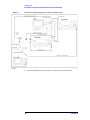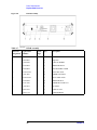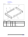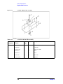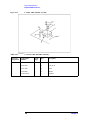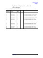
1
Agilent 43521A Downconverter Unit
Service Manual
First Edition
SERIAL NUMBERS
This manual applies directly to instruments that have the serial number
JP1KG 143/146, and JP1KG00150 or above. For additional important
information about serial numbers, see Appendix A.
Part No. 43521-90100
February 2000
Printed in Japan
Notices
The information contained in this document is subject to change without notice.
This document contains proprietary information that is protected by copyright. All rights
are reserved. No part of this document may be photocopied, reproduced, or translated into
another language without the prior written consent of Agilent Technologies.
Agilent Technologies Japan, Ltd.
Component Test PGU-Kobe
1-3-2, Murotani, Nishi-Ku, Kobe-shi, Hyogo, 651-2241 Japan
Copyright © Agilent Technologies Japan, Ltd. 2000
Manual Printing History
The manual’s printing date and part number indicate its current edition. The printing date
changes when a new edition is printed. (Minor corrections and updates incorporated in
reprints do not necessitate a new printing date.) The manual part number changes when
extensive technical changes are incorporated.
Feb. 2000
First Edition
Safety Summary
The following general safety precautions must be observed during all phases of operation,
service, and repair of this instrument. Failure to comply with these precautions or with
specific WARNINGS elsewhere in this manual may impair the protection provided by the
equipment. Such noncompliance would also violate safety standards of design,
manufacture, and intended use of the instrument.
The Agilent Technologies assumes no liability for the customer’s failure to comply with
these requirements.
NOTE
The Agilent 43521A complies with INSTALLATION CATEGORY II and POLLUTION
DEGREE 2 in IEC61010-1. The Agilent 43521A is an INDOOR USE product.
NOTE
LEDs in the Agilent 43521A are Class 1 in accordance with IEC60825-1,
CLASS 1 LED PRODUCT.
•
Ground the Instrument
To avoid electric shock, the instrument chassis and cabinet must be grounded with the
supplied power cable’s grounding prong.
2
•
DO NOT Operate in an Explosive Atmosphere
Do not operate the instrument in the presence of inflammable gasses or fumes.
Operation of any electrical instrument in such an environment clearly constitutes a
safety hazard.
•
Keep Away from Live Circuits
Operators must not remove instrument covers. Component replacement and internal
adjustments must be made by qualified maintenance personnel. Do not replace
components with the power cable connected. Under certain conditions, dangerous
voltage levels may exist even with the power cable removed. To avoid injuries, always
disconnect the power and discharge circuits before touching them.
•
DO NOT Service or Adjust Alone
Do not attempt internal service or adjustment unless another person, capable of
rendering first aid and resuscitation, is present.
•
DO NOT Substitute Parts or Modify the Instrument
To avoid the danger of introducing additional hazards, do not install substitute parts or
perform unauthorized modifications to the instrument. Return the instrument to an
Agilent Technologies Sales and Service Office for service and repair to ensure that
safety features are maintained in operational condition.
•
Dangerous Procedure Warnings
Warnings, such as the example below, precede potentially dangerous procedures
throughout this manual. Instructions contained in the warnings must be followed.
WARNING
Dangerous voltage levels, capable of causing death, are present in this instrument.
Use extreme caution when handling, testing, or adjusting this instrument.
Safety Symbols
General definitions of safety symbols used on the instrument or in manuals are listed
below.
Instruction Manual symbol: the product is marked with this symbol when it is necessary for
the user to refer to the instrument manual.
Alternating current.
Direct current.
On (Supply).
Off (Supply).
In-position of push-button switch.
Out-position of push-button switch.
Frame (or chassis) terminal. A connection to the frame (chassis) of the equipment, which
normally include all exposed metal structure.
3
WARNING
This warning sign denotes a hazard. It calls attention to a procedure, practice, or
condition that, if not correctly performed or adhered to, could result in injury or
death to personnel.
CAUTION
This Caution sign denotes a hazard. It calls attention to a procedure, practice, or condition
that, if not correctly performed or adhered to, could result in damage to or destruction of
part or all of the product.
NOTE
This Note sign denotes important information. It calls attention to a procedure, practice, or
condition that is essential for the user to understand.
Certification
Agilent Technologies certifies that this product met its published specifications at the time
of shipment from the factory. Agilent Technologies further certifies that its calibration
measurements are traceable to the United States National Institute of Standards and
Technology, to the extent allowed by the Institution’s calibration facility or by the
calibration facilities of other International Standards Organization members.
Warranty
This Agilent Technologies instrument product is warranted against defects in material and
workmanship for a period corresponding to the individual warranty periods of its
component products. Instruments are warranted for a period of one year. Fixtures and
adapters are warranted for a period of 90 days. During the warranty period, Agilent
Technologies will, at its option, either repair or replace products that prove to be defective.
For warranty service or repair, this product must be returned to a service facility designated
by Agilent Technologies. Buyer shall prepay shipping charges to Agilent Technologies and
Agilent Technologies shall pay shipping charges to return the product to Buyer. However,
Buyer shall pay all shipping charges, duties, and taxes for products returned to Agilent
Technologies from another country.
Agilent Technologies warrants that its software and firmware designated by Agilent
Technologies for use with an instrument will execute its programming instruction when
properly installed on that instrument. Agilent Technologies does not warrant that the
operation of the instrument, or software, or firmware will be uninterrupted or error free.
4
Limitation of Warranty
The foregoing warranty shall not apply to defects resulting from improper or inadequate
maintenance by Buyer, Buyer-supplied software or interfacing, unauthorized modification
or misuse, operation outside the environmental specifications for the product, or improper
site preparation or maintenance.
IMPORTANT
No other warranty is expressed or implied. Agilent Technologies specifically disclaims the
implied warranties of merchantability and fitness for a particular purpose.
Exclusive Remedies
The remedies provided herein are Buyer’s sole and exclusive remedies. Agilent
Technologies shall not be liable for any direct, indirect, special, incidental, or
consequential damages, whether based on contract, tort, or any other legal theory.
Assistance
Product maintenance agreements and other customer assistance agreements are available
for Agilent Technologies products.
For any assistance, contact your nearest Agilent Technologies Sales and Service Office.
Addresses are provided at the back of this manual.
Typeface Conventions
Bold
Boldface type is used when a term is defined. For
example: icons are symbols.
Italic
Italic type is used for emphasis and for titles of
manuals and other publications.
[Hardkey]
Indicates a hardkey labeled “Hardkey.”
Softkey
Indicates a softkey labeled “Softkey.”
[Hardkey] - Softkey1 - Softkey2
Indicates keystrokes [Hardkey] - Softkey1 Softkey2.
5
6
Contents
1. General Information
Organization of Service Manual . . . . . . . . . . . . . . . . . . . . . . . . . . . . . . . . . . . . . . . . . . . . . . . . . . . . . . . . . . 12
Instruments Covered by This Manual. . . . . . . . . . . . . . . . . . . . . . . . . . . . . . . . . . . . . . . . . . . . . . . . . . . . . . 13
Require Equipment . . . . . . . . . . . . . . . . . . . . . . . . . . . . . . . . . . . . . . . . . . . . . . . . . . . . . . . . . . . . . . . . . . . . 14
2. Performance Test
Performance Test . . . . . . . . . . . . . . . . . . . . . . . . . . . . . . . . . . . . . . . . . . . . . . . . . . . . . . . . . . . . . . . . . . . . . 18
Introduction . . . . . . . . . . . . . . . . . . . . . . . . . . . . . . . . . . . . . . . . . . . . . . . . . . . . . . . . . . . . . . . . . . . . . . . . 18
RF Power Measurement Accuracy Test . . . . . . . . . . . . . . . . . . . . . . . . . . . . . . . . . . . . . . . . . . . . . . . . . . 19
Input VSWR Test . . . . . . . . . . . . . . . . . . . . . . . . . . . . . . . . . . . . . . . . . . . . . . . . . . . . . . . . . . . . . . . . . . . 23
Function Test. . . . . . . . . . . . . . . . . . . . . . . . . . . . . . . . . . . . . . . . . . . . . . . . . . . . . . . . . . . . . . . . . . . . . . . . . 26
Introduction . . . . . . . . . . . . . . . . . . . . . . . . . . . . . . . . . . . . . . . . . . . . . . . . . . . . . . . . . . . . . . . . . . . . . . . . 26
Warm Up Time . . . . . . . . . . . . . . . . . . . . . . . . . . . . . . . . . . . . . . . . . . . . . . . . . . . . . . . . . . . . . . . . . . . . . 26
Ambient Condition . . . . . . . . . . . . . . . . . . . . . . . . . . . . . . . . . . . . . . . . . . . . . . . . . . . . . . . . . . . . . . . . . . 26
600 MHz SAW OSC Phase Noise Test . . . . . . . . . . . . . . . . . . . . . . . . . . . . . . . . . . . . . . . . . . . . . . . . . . . 27
System Phase Noise Test. . . . . . . . . . . . . . . . . . . . . . . . . . . . . . . . . . . . . . . . . . . . . . . . . . . . . . . . . . . . . . 29
Calculation Sheet . . . . . . . . . . . . . . . . . . . . . . . . . . . . . . . . . . . . . . . . . . . . . . . . . . . . . . . . . . . . . . . . . . . . . 32
Performance Test. . . . . . . . . . . . . . . . . . . . . . . . . . . . . . . . . . . . . . . . . . . . . . . . . . . . . . . . . . . . . . . . . . . . 32
Function Test . . . . . . . . . . . . . . . . . . . . . . . . . . . . . . . . . . . . . . . . . . . . . . . . . . . . . . . . . . . . . . . . . . . . . . . 34
Performance Test Record . . . . . . . . . . . . . . . . . . . . . . . . . . . . . . . . . . . . . . . . . . . . . . . . . . . . . . . . . . . . . . . 35
RF Power Measurement Accuracy Test . . . . . . . . . . . . . . . . . . . . . . . . . . . . . . . . . . . . . . . . . . . . . . . . . . 35
Input VSWR Test . . . . . . . . . . . . . . . . . . . . . . . . . . . . . . . . . . . . . . . . . . . . . . . . . . . . . . . . . . . . . . . . . . . 36
Function Test Record . . . . . . . . . . . . . . . . . . . . . . . . . . . . . . . . . . . . . . . . . . . . . . . . . . . . . . . . . . . . . . . . 36
600 MHz SAW OSC Phase Noise Test . . . . . . . . . . . . . . . . . . . . . . . . . . . . . . . . . . . . . . . . . . . . . . . . . . . 36
System Phase Noise Test. . . . . . . . . . . . . . . . . . . . . . . . . . . . . . . . . . . . . . . . . . . . . . . . . . . . . . . . . . . . . . 36
3. Adjustment
Safety Considerations . . . . . . . . . . . . . . . . . . . . . . . . . . . . . . . . . . . . . . . . . . . . . . . . . . . . . . . . . . . . . . . . . . 38
Required Controller . . . . . . . . . . . . . . . . . . . . . . . . . . . . . . . . . . . . . . . . . . . . . . . . . . . . . . . . . . . . . . . . . . . 38
Warm-up for Adjustment . . . . . . . . . . . . . . . . . . . . . . . . . . . . . . . . . . . . . . . . . . . . . . . . . . . . . . . . . . . . . . . 38
Required Equipment . . . . . . . . . . . . . . . . . . . . . . . . . . . . . . . . . . . . . . . . . . . . . . . . . . . . . . . . . . . . . . . . . . . 38
Order of Adjustment . . . . . . . . . . . . . . . . . . . . . . . . . . . . . . . . . . . . . . . . . . . . . . . . . . . . . . . . . . . . . . . . . . . 39
Preparation for using the Adjustment Program . . . . . . . . . . . . . . . . . . . . . . . . . . . . . . . . . . . . . . . . . . . . . . 40
Installing a GPIB Card (82340B, 82341C/D or 82350A). . . . . . . . . . . . . . . . . . . . . . . . . . . . . . . . . . . . . 40
Installing HP VEE for Personal Computer . . . . . . . . . . . . . . . . . . . . . . . . . . . . . . . . . . . . . . . . . . . . . . . . 40
Installing Adjustment Program into Your PC (preliminary) . . . . . . . . . . . . . . . . . . . . . . . . . . . . . . . . . . . 40
Equipment Setup . . . . . . . . . . . . . . . . . . . . . . . . . . . . . . . . . . . . . . . . . . . . . . . . . . . . . . . . . . . . . . . . . . . . 40
Running the Adjustment Program . . . . . . . . . . . . . . . . . . . . . . . . . . . . . . . . . . . . . . . . . . . . . . . . . . . . . . . . 42
600 MHz SAW Oscillator Frequency Adjustment . . . . . . . . . . . . . . . . . . . . . . . . . . . . . . . . . . . . . . . . . . . . 43
Required Equipment . . . . . . . . . . . . . . . . . . . . . . . . . . . . . . . . . . . . . . . . . . . . . . . . . . . . . . . . . . . . . . . . . 43
Manual Procedure . . . . . . . . . . . . . . . . . . . . . . . . . . . . . . . . . . . . . . . . . . . . . . . . . . . . . . . . . . . . . . . . . . . 43
Writing Default Correction Constant . . . . . . . . . . . . . . . . . . . . . . . . . . . . . . . . . . . . . . . . . . . . . . . . . . . . . . 45
Required Equipment . . . . . . . . . . . . . . . . . . . . . . . . . . . . . . . . . . . . . . . . . . . . . . . . . . . . . . . . . . . . . . . . . 45
Procedure. . . . . . . . . . . . . . . . . . . . . . . . . . . . . . . . . . . . . . . . . . . . . . . . . . . . . . . . . . . . . . . . . . . . . . . . . . 45
RF Power Linearity Correction Constants . . . . . . . . . . . . . . . . . . . . . . . . . . . . . . . . . . . . . . . . . . . . . . . . . . 46
Required Equipment . . . . . . . . . . . . . . . . . . . . . . . . . . . . . . . . . . . . . . . . . . . . . . . . . . . . . . . . . . . . . . . . . 46
Procedure. . . . . . . . . . . . . . . . . . . . . . . . . . . . . . . . . . . . . . . . . . . . . . . . . . . . . . . . . . . . . . . . . . . . . . . . . . 47
RF Power Frequency Response Correction Constants . . . . . . . . . . . . . . . . . . . . . . . . . . . . . . . . . . . . . . . . . 48
7
Contents
Required Equipment . . . . . . . . . . . . . . . . . . . . . . . . . . . . . . . . . . . . . . . . . . . . . . . . . . . . . . . . . . . . . . . . . 48
Procedure . . . . . . . . . . . . . . . . . . . . . . . . . . . . . . . . . . . . . . . . . . . . . . . . . . . . . . . . . . . . . . . . . . . . . . . . . 49
4. Troubleshooting
TROUBLESHOOTING SUMMARY . . . . . . . . . . . . . . . . . . . . . . . . . . . . . . . . . . . . . . . . . . . . . . . . . . . . .
Check Procedure . . . . . . . . . . . . . . . . . . . . . . . . . . . . . . . . . . . . . . . . . . . . . . . . . . . . . . . . . . . . . . . . . . . . .
Check LED (Front) . . . . . . . . . . . . . . . . . . . . . . . . . . . . . . . . . . . . . . . . . . . . . . . . . . . . . . . . . . . . . . . . . .
Check Fan . . . . . . . . . . . . . . . . . . . . . . . . . . . . . . . . . . . . . . . . . . . . . . . . . . . . . . . . . . . . . . . . . . . . . . . . .
Check 600 MHz Output . . . . . . . . . . . . . . . . . . . . . . . . . . . . . . . . . . . . . . . . . . . . . . . . . . . . . . . . . . . . . .
Check Power Measurement Function . . . . . . . . . . . . . . . . . . . . . . . . . . . . . . . . . . . . . . . . . . . . . . . . . . . .
Check Heterodyne Path . . . . . . . . . . . . . . . . . . . . . . . . . . . . . . . . . . . . . . . . . . . . . . . . . . . . . . . . . . . . . .
Check Local Doubler Path . . . . . . . . . . . . . . . . . . . . . . . . . . . . . . . . . . . . . . . . . . . . . . . . . . . . . . . . . . . .
Power Supply Troubleshooting . . . . . . . . . . . . . . . . . . . . . . . . . . . . . . . . . . . . . . . . . . . . . . . . . . . . . . . . . .
Check the Line Voltage, and Fuse. . . . . . . . . . . . . . . . . . . . . . . . . . . . . . . . . . . . . . . . . . . . . . . . . . . . . . .
Check the Power Supply Unit Output. . . . . . . . . . . . . . . . . . . . . . . . . . . . . . . . . . . . . . . . . . . . . . . . . . . .
Check the Power Supply on the A1 board . . . . . . . . . . . . . . . . . . . . . . . . . . . . . . . . . . . . . . . . . . . . . . . .
600 MHz OSC Troubleshooting. . . . . . . . . . . . . . . . . . . . . . . . . . . . . . . . . . . . . . . . . . . . . . . . . . . . . . . . . .
Check the 600 MHz Output on the A1 board . . . . . . . . . . . . . . . . . . . . . . . . . . . . . . . . . . . . . . . . . . . . . .
Power Measurement Function Troubleshooting. . . . . . . . . . . . . . . . . . . . . . . . . . . . . . . . . . . . . . . . . . . . . .
Heterodyne Path Troubleshooting . . . . . . . . . . . . . . . . . . . . . . . . . . . . . . . . . . . . . . . . . . . . . . . . . . . . . . . .
Local Doubler Path Troubleshooting . . . . . . . . . . . . . . . . . . . . . . . . . . . . . . . . . . . . . . . . . . . . . . . . . . . . . .
Performance/Function Tests Failure Troubleshooting . . . . . . . . . . . . . . . . . . . . . . . . . . . . . . . . . . . . . . . . .
Perform Adjustments and Correction Constants . . . . . . . . . . . . . . . . . . . . . . . . . . . . . . . . . . . . . . . . . . .
52
54
54
54
54
55
55
57
59
59
59
60
62
62
64
66
69
71
71
5. Theory of Operation
OVERALL OPERATION . . . . . . . . . . . . . . . . . . . . . . . . . . . . . . . . . . . . . . . . . . . . . . . . . . . . . . . . . . . . . .
43521A BLOCK DIAGRAM . . . . . . . . . . . . . . . . . . . . . . . . . . . . . . . . . . . . . . . . . . . . . . . . . . . . . . . . . .
Power Supply Section . . . . . . . . . . . . . . . . . . . . . . . . . . . . . . . . . . . . . . . . . . . . . . . . . . . . . . . . . . . . . . . .
Sequencer & I/O (Digital Control) Section . . . . . . . . . . . . . . . . . . . . . . . . . . . . . . . . . . . . . . . . . . . . . . .
Power Measurement Section . . . . . . . . . . . . . . . . . . . . . . . . . . . . . . . . . . . . . . . . . . . . . . . . . . . . . . . . . .
Heterodyne Section. . . . . . . . . . . . . . . . . . . . . . . . . . . . . . . . . . . . . . . . . . . . . . . . . . . . . . . . . . . . . . . . . .
Local Drive Section . . . . . . . . . . . . . . . . . . . . . . . . . . . . . . . . . . . . . . . . . . . . . . . . . . . . . . . . . . . . . . . . .
600 MHz OSC Section . . . . . . . . . . . . . . . . . . . . . . . . . . . . . . . . . . . . . . . . . . . . . . . . . . . . . . . . . . . . . . .
74
75
77
77
77
78
78
78
6. Parts Replacement
Replaceable Part List . . . . . . . . . . . . . . . . . . . . . . . . . . . . . . . . . . . . . . . . . . . . . . . . . . . . . . . . . . . . . . . . . . 80
Ordering Information . . . . . . . . . . . . . . . . . . . . . . . . . . . . . . . . . . . . . . . . . . . . . . . . . . . . . . . . . . . . . . . . 80
. . . . . . . . . . . . . . . . . . . . . . . . . . . . . . . . . . . . . . . . . . . . . . . . . . . . . . . . . . . . . . . . . . . . . . . . . . . . . . . . . 80
Parts List . . . . . . . . . . . . . . . . . . . . . . . . . . . . . . . . . . . . . . . . . . . . . . . . . . . . . . . . . . . . . . . . . . . . . . . . . . 81
Replacement Procedure . . . . . . . . . . . . . . . . . . . . . . . . . . . . . . . . . . . . . . . . . . . . . . . . . . . . . . . . . . . . . . . 105
Top Cover Removal . . . . . . . . . . . . . . . . . . . . . . . . . . . . . . . . . . . . . . . . . . . . . . . . . . . . . . . . . . . . . . . . 105
Bottom Cover Removal . . . . . . . . . . . . . . . . . . . . . . . . . . . . . . . . . . . . . . . . . . . . . . . . . . . . . . . . . . . . . 105
Side Cover Removal . . . . . . . . . . . . . . . . . . . . . . . . . . . . . . . . . . . . . . . . . . . . . . . . . . . . . . . . . . . . . . . . 105
Front Panel Removal . . . . . . . . . . . . . . . . . . . . . . . . . . . . . . . . . . . . . . . . . . . . . . . . . . . . . . . . . . . . . . . 106
Rear Panel Removal . . . . . . . . . . . . . . . . . . . . . . . . . . . . . . . . . . . . . . . . . . . . . . . . . . . . . . . . . . . . . . . . 106
Step Attenuator Replacement . . . . . . . . . . . . . . . . . . . . . . . . . . . . . . . . . . . . . . . . . . . . . . . . . . . . . . . . . 107
U-WAVE AMP 18 GHz Replacement . . . . . . . . . . . . . . . . . . . . . . . . . . . . . . . . . . . . . . . . . . . . . . . . . . 107
U-WAVE MXR 26.5 GHz Replacement. . . . . . . . . . . . . . . . . . . . . . . . . . . . . . . . . . . . . . . . . . . . . . . . . 108
8
Contents
U-WAVE AMP 20 GHz Replacement. . . . . . . . . . . . . . . . . . . . . . . . . . . . . . . . . . . . . . . . . . . . . . . . . . . 108
U-WAVE FREQ DBLR Replacement. . . . . . . . . . . . . . . . . . . . . . . . . . . . . . . . . . . . . . . . . . . . . . . . . . . 109
U-WAVE AMP 700 MHz Replacement . . . . . . . . . . . . . . . . . . . . . . . . . . . . . . . . . . . . . . . . . . . . . . . . . 109
7. Post Repair Procedures
POST REPAIR PROCEDURES. . . . . . . . . . . . . . . . . . . . . . . . . . . . . . . . . . . . . . . . . . . . . . . . . . . . . . . . . 112
A. Manual Changes
Manual Changes . . . . . . . . . . . . . . . . . . . . . . . . . . . . . . . . . . . . . . . . . . . . . . . . . . . . . . . . . . . . . . . . . . . . . 116
Change 1 . . . . . . . . . . . . . . . . . . . . . . . . . . . . . . . . . . . . . . . . . . . . . . . . . . . . . . . . . . . . . . . . . . . . . . . . . . . 117
Page 57, Check Heterodyne Path . . . . . . . . . . . . . . . . . . . . . . . . . . . . . . . . . . . . . . . . . . . . . . . . . . . . . . 117
Page 57, Check Local Doubler Path . . . . . . . . . . . . . . . . . . . . . . . . . . . . . . . . . . . . . . . . . . . . . . . . . . . . 117
Page 64, Figure 4-7 Power Measurement Section Simplified Block Diagram . . . . . . . . . . . . . . . . . . . . 118
Page 66, Figure 4-9 Heterodyne Path Simplified Block Diagram . . . . . . . . . . . . . . . . . . . . . . . . . . . . . 119
Page 68, Heterodyne Path Troubleshooting . . . . . . . . . . . . . . . . . . . . . . . . . . . . . . . . . . . . . . . . . . . . . . 119
Page 70, Local Doubler Path Troubleshooting . . . . . . . . . . . . . . . . . . . . . . . . . . . . . . . . . . . . . . . . . . . . 120
Page 76, Figure 5-2 43521A Block Diagram . . . . . . . . . . . . . . . . . . . . . . . . . . . . . . . . . . . . . . . . . . . . . 121
Page 82, Figure 6-2 Top View (Major Assemblies) . . . . . . . . . . . . . . . . . . . . . . . . . . . . . . . . . . . . . . . . 122
Page 83, Table 6-1 Top View (Major Assemblies) . . . . . . . . . . . . . . . . . . . . . . . . . . . . . . . . . . . . . . . . . 123
Page 84, Figure 6-3 Top View (Cables and Wires 1/2) . . . . . . . . . . . . . . . . . . . . . . . . . . . . . . . . . . . . . . 124
Page 85, Table 6-2 Top View (Cables and Wires 1/2). . . . . . . . . . . . . . . . . . . . . . . . . . . . . . . . . . . . . . . 125
Page 86, Figure 6-4 Top View (Cables and Wires 2/2) . . . . . . . . . . . . . . . . . . . . . . . . . . . . . . . . . . . . . . 126
Page 87, Table 6-3 Top View (Cables and Wires 2/2). . . . . . . . . . . . . . . . . . . . . . . . . . . . . . . . . . . . . . . 127
Page 97, Figure 6-12 Step Attenuator Assembly . . . . . . . . . . . . . . . . . . . . . . . . . . . . . . . . . . . . . . . . . . 128
Page 97, Table 6-11 Step Attenuator Assembly . . . . . . . . . . . . . . . . . . . . . . . . . . . . . . . . . . . . . . . . . . . 128
Page 103, Figure 6-18 DETECTOR Assembly. . . . . . . . . . . . . . . . . . . . . . . . . . . . . . . . . . . . . . . . . . . . 129
Page 103, Table 6-17 DETECTOR Assembly . . . . . . . . . . . . . . . . . . . . . . . . . . . . . . . . . . . . . . . . . . . . 129
Page 107, Step Attenuator Replacement . . . . . . . . . . . . . . . . . . . . . . . . . . . . . . . . . . . . . . . . . . . . . . . . . 130
Page 107, U-WAVE AMP 18 GHz Replacement . . . . . . . . . . . . . . . . . . . . . . . . . . . . . . . . . . . . . . . . . . 131
Pages 112, Table 7-1 Post Repair Procedures . . . . . . . . . . . . . . . . . . . . . . . . . . . . . . . . . . . . . . . . . . . . . 132
B. Power Requirement
Replacing Fuse . . . . . . . . . . . . . . . . . . . . . . . . . . . . . . . . . . . . . . . . . . . . . . . . . . . . . . . . . . . . . . . . . . . . . . 136
Fuse Selection . . . . . . . . . . . . . . . . . . . . . . . . . . . . . . . . . . . . . . . . . . . . . . . . . . . . . . . . . . . . . . . . . . . . . 136
Power Requirements . . . . . . . . . . . . . . . . . . . . . . . . . . . . . . . . . . . . . . . . . . . . . . . . . . . . . . . . . . . . . . . . . . 137
Power Cable . . . . . . . . . . . . . . . . . . . . . . . . . . . . . . . . . . . . . . . . . . . . . . . . . . . . . . . . . . . . . . . . . . . . . . 137
9
Contents
10
1
General Information
The Service Manual is a guide to servicing the 43521A Downconverter Unit. The manual
contains informatoin required to performance test, adjust, troubleshoot, and repair the
Downconverter unit
11
General Information
Organization of Service Manual
Organization of Service Manual
The 43521A is used as part of the 4352S VCO/PLL Signal Test System. Using the 43521A
expands the maximum frequency of the 4352S to 12.6 GHz.
This manual consists of the chapters and appendices listed below,. This section lists the
names of the chapters and the desrcibes content of each chapter and the appendices.
•
Performance Test provides the procedures required to performance test for the
43521A.
•
Adjustment provides procedures for adjusting the 43521A after repair or replacement of
a part. Most of the adjustments update the correction constants data stored in the
EEPROM on the A1 board assembly. The correction constants data is updated by using
the adjustment program.
•
Troubleshooting outlines the 43521A troubleshooting, and provides troubleshooting
procedures to isolate the faulty part.
•
Theory of Operation explains the overall operation of the 43521A.
•
Parts Replacement provides the replaceable part list and the procedure to replace its
assemblies.
•
Post Repair Procedures contains the table of related service procedures. It is a table of
adjustments and verification procedures to be performed after repair or replacement of
each part.
•
Appendices contains manual change information (required to make this manual
compatible with earlier shipment configurations of the 43521A), and power
requirements of the 43521A.
12
Chapter 1
General Information
Instruments Covered by This Manual
Instruments Covered by This Manual
Agilent Technologies uses a two-part, ten-character serial number label (See Figure 1-1)
attached to the instrument’s rear panel. The first five characters are the serial prefix and the
last five digits are the suffix.
Figure 1-1
Serial Number Label
An instrument manufactured after the printing date of this manual may have serial number
prefix that is not listed on the title page. This unlisted serial number prefix indicates the
instrument is different from those described in this manual. The manual for this new
instrument may be accompanied by a yellow Manual Changes supplement or have a
different manual part number. This sheet contains “change information” that explains how
to adapt the manual to the newer instrument.
In addition to change information, the supplement may contain information for correcting
errors (Errata) in the manual. To keep this manual as current and accurate as possible,
Agilent Technologies recommends that you periodically request the latest Manual Changes
supplement. The supplement for this manual is identified by this manual’s printing data
and is available from Agilent Technologies. If the serial prefix or number of an instrument
is lower than that on the title page of this manual, see Appendix A, Manual Changes. For
information concerning, a serial number prefix that is not listed on the title page or in the
Manual change supplement, contact the nearest Agilent Technologies office.
Chapter 1
13
General Information
Require Equipment
Require Equipment
Table 1-1 lists the recommended equipment for performing maintenance on the 43521A.
Table 1-1
Recommended Test Equipment
Equipment
Critical Specifications
Recommended Model
Qty.
Use*1
VCO/PLL Signal
Analyzer
No substitute
4352B
1
P,A,
T
Signal Generator
Freq.Range 10 MHz to 6 GHz
Power: ≥ 10 dBm
8665B Opt.004 or
8360B series
1
P,A,
T
Signal Generator
Freq Range 10 MHz to 3 GHz
Power:
8664A Opt.004
8665A/B Opt.004
or 8642B
1
P
Signal Generator
Freq Rang 3 GHz to 12 GHz
83711B or 8360B series
1
P,A,
T
Power Meter
No substitute
437B, 438A,
E4418A/B or E4419A/B
1
P,A
Power Meter
No substitute
E4419A/B
1
A
Power Sensor
Freq. Range: 3 GHz to 12 GHz,
Power: +15 dBm to −15 dBm
8481A
2
P,A
Power Sensor
No substitute
E4412A
1
A
Power Amplifier
Gain: 35 dB
Freq. Range: 3 GHz to 12 GHz
83020A
1
P,A
DC Power Supply
No substitute
87422A (for 83020A)
1
P,A
Network Analyzer
Freq: 2 GHz to 13 GHz
8719D, 8720D
or 8722D
1
P
Calibration Kit
Freq: 2 GHz to 13 GHz
85054D or 85054B
1
P
Step Attenuator
Attenuation Range: 0 dB to 70 dB,
Step: 10 dB,
Freq.Range: 3 GHz to 12 GHz
8495H
1
P,A
Step Attenuator
Attenuation Range: 0 dB to 11 dB,
Step: 1 dB,
Freq.Range: 3 GHz to 12 GHz
8494H
1
P,A
Att. Switch Driver
No substitute
11713A
1
P,A
Power Splitter
Freq. Range: 3 GHz to 12 GHz
2-Way, 50 Ω
11667A
1
P,A
2 GHz Lowpass Filter
Insertion Loss: 0.5 dB,
VSWR < 1.24
p/n 0955-0634
1
A
14
Chapter 1
General Information
Require Equipment
Table 1-1
Recommended Test Equipment
Equipment
Critical Specifications
Recommended Model
Qty.
Use*1
Attenuator Pad
Impedance 50 Ω, 7mm(m)-7mm(f),
6 dB, 3 GHz to 12 GHz
8493B Opt.006
1
P,A
Blocking Capacitor
No substitute
11742A
1
P,A
Spectrum Analyzer
Freq. Range: 100 MHz to 5 GHz
8595E
1
T
Cable
N(m)-N(m),18 cm
8120-4387
2
P,A,
T
N(m)-N(m),61 cm
11500B
1
P,A,
T
BNC(m)-BNC(m),61 cm
8120-1839
2
P,A,
T
BNC(m)-BNC(m),122 cm
8120-1840
1
P,A,
T
Precision N(m)-Precison
N(m),61cm
11500C
2
P,A,
T
3.5mm(m)-3.5mm(m) Cable,61cm
11500E
1
P,A,
T
N(m)-N(m) Adapter
1250-1475
1
P
SMA(f)-SMA(f) Adapter
1250-1158
1
T
SMA right angle(m)(f) Adapter
1250-1249
2
T
3.5mm(f)-Precision N(m) Adapter
1250-1744
2
P,A,
T
3.5mm(m)-Precision N(f) Adapter
1250-1750
1
A
3.5mm(m)-N(m) Adapter
1250-1743
1
A
3.5mm(f)*2-N(f) Adapter
part of 85130C*3
1
P
Adapter
*1.P: Performance Test, A: Adjustment and Correction Constants, T: Troubleshooting
*2.Special rugged female connector specifically for connecting to the network analyzer test port, but does not mate
with a standard male connector.
*3.If the 8722D is used, use 87130E+ 11524A for a substitute.
Chapter 1
15
General Information
Require Equipment
16
Chapter 1
2
Performance Test
This chapter provides the Performance Test Procedure for the 43521A Downconverter
Unit. These performance tests are used to verify that the analyzer’s performance meets its
specifications.
17
Performance Test
Performance Test
Performance Test
Introduction
This section provides the test procedures used to verify that the 43521A’s specifications
are met. The performance tests can also be used for incoming inspection, and for
verification after troubleshooting or adjustment. If the performance tests indicate that the
43521A is NOT operating within the specified limits, check your test setup, then proceed
with troubleshooting if necessary.
Warm Up Time
Allow the 43521A to warm up for at least 30 minutes before you execute any of the
performance tests.
Ambient Conditions
Perform all performance tests in ambient conditions of 23 °C ± 5 °C, ≤ 70% RH.
Performance Test Interval
The performance test should be performed periodically. The recommended test interval is
12 months.
NOTE
The test interval depends on maintenance of use and the environmental conditions under
which the instrument is used. You may find that the test interval could be shortened or
lengthened; however, such a decision should be based on substantial quantitative data.
Performance Test Record and Calculation Sheet
Performance test record lists all test points, acceptable test limits, test result entry columns,
and measurement uncertainties. The listed measurement uncertainties are valid only when
the recommended test equipment is used.
The calculation sheet is used as an aid for recording raw measurement data, and for
calculating the performance test results.
The procedure for using the calculation sheet and performance test record is;
1. Photo copy the calculation sheet.
2. Follow the performance test procedure and record the measurement values, etc., in the
specified column on the calculation sheet.
3. Calculate the test result using the appropriate equation given on the calculation sheet,
and record the test result into the Test Result column of the performance test record.
18
Chapter 2
Performance Test
Performance Test
RF Power Measurement Accuracy Test
This test checks the RF power measurement accuracy.
Specification
RF Power Measurement Accuracy
Frequency
Level (Attenuator)
Temperature
≥2.4 GHz, ≤4 GHz
> 4 GHz, ≤8 GHz
> 8 GHz, ≤ 12 GHz
≤ 0 dBm (0 dB)
23±10 °C
±1.5 dB
±2.0 dB
±2.5 dB
≤ 15 dBm (> 0dB)
0 to 40 °C
±1.5 dB
±2.0 dB
±2.5 dB
Test Equipment
Description
Recommended Model
Signal Generator (for RF IN)
83711B or 8360B series
Signal Generator (for LO IN)
8665B or 8360B series
Power Amplifier
83020A
DC Power Supply
87422A
Power Splitter
11667A
Power Meter
E4418A/B,437B,or 438A
Power Sensor
8481A
VCO/PLL Signal Analyzer
4352B
Step Attenuator
8495H
Step Attenuator
8494H
Attenuator Pad
8493B Opt.006
Blocking Capacitor
11742A
RF Cable N(m)-N(m), 61 cm
p/n 8120-1839,2ea
RF Cable N(m)-N(m), 122 cm
p/n 8120-1840
N(m)-N(m) Cable,18cm
p/n 8120-4387,2ea
N(m)-N(m) Cable, 61cm
11500B or part of 11851B
Precision N(m)-Precision N(m)
Cable, 61 cm
11500C or part of 11851B,
2ea
3.5mm(m)-3.5mm(m) Cable,61 cm
11500E
N(m)-N(m) Adapter
1250-1475
3.5mm(m)-Precision N(f) Adapter
1250-1744
Chapter 2
19
Performance Test
Performance Test
Procedure
Figure 2-1
Power Measurement Accuracy Test Setup
1. Perform the zero adjustment and the calibration for the power meter.
2. Connect the equipment as shown in Figure 2-1.
3. Press [Preset] to initialize the 4352B. Then set the controls as follows.
20
Chapter 2
Performance Test
Performance Test
Setting
Operation
Instrument type: VCO Tester
[Meas] - INST TYPE - VCO TESTER
Measurement mode: RF Power
[Meas] - RF POWER
Down converter control: ON
[RF/LO] - DOWNCONV ON off
LO control: Auto*1
[RF/LO] - LO CONTROL AUTO man
Signal generator type: 1*2
[RF/LO] - SG TYPE - [1]
Signal generator max. freq.: 6 GHz
[RF/LO] - SG MAX FREQ - [6] - [G/n]
Frequency Band: 2.4 GHz-6.6 GHz
[Meas] - FREQ BAND - 2.4-6.6G
Nominal Frequency: 4 GHz
[Meas] - FREQ BAND - NOMINAL FREQ - [4] [G/n]
43521A RF Attenuator: 20 dB
[Sense Range] - RF ATTEN - [2] - [0] - [×1]
*1.If the signal generator for the LO IN port is NOT the 8665B, set the LO control to Manual.
*2.If the LO control is set to Manual, this operation is not required.
4. Set the other instruments’ control as follows.
Instrument
Setting
RF signal generator
Freq: 4 GHz, Power: 0 dBm
LO signal generator*1
Freq: 4.624 GHz, Power: 10 dBm
Step Attenuator
0 dB
*1.If the LO control is set to Auto, this operation is NOT required.
5. Adjust the RF signal generator output power to make the power meter reading between
(15±0.2) dBm.
6. Record the 4352B reading and the power meter reading in the calculation sheet.
7. Calculate the test result according to the calculation sheet, then record it in the
performance test record.
8. Repeat Step 6 for all setting in Table 2-1
Chapter 2
21
Performance Test
Performance Test
Table 2-1
Power Measurement Accuracy Test Setting
RF Att.
Power
Meter
Reading
RF SG
Freq.
Step Att.
LO SG
Freq.*1
Freq. Band
20 dB
15±0.2 dBm
4 GHz
0 dB
4.624 GHz
2.4 to 6.6 GHz
8 GHz
0 dB
3.688 GHz
5.4 to12.6 GHz
12 GHz
0 dB
5.688 GHz
5.4 to12.6 GHz
4 GHz
10 dB
4.624 GHz
2.4 to 6.6 GHz
8 GHz
10 dB
3.688 GHz
5.4 to 12.6 GHz
12 GHz
10 dB
5.688 GHz
5.4 to 12.6 GHz
3 GHz
15 dB
3.624 GHz
2.4 to 6.6 GHz
4 GHz
15 dB
4.624 GHz
2.4 to 6.6 GHz
5 GHz
15 dB
5.624 GHz
2.4 to 6.6 GHz
6 GHz
15 dB
2.688 GHz
5.4 to 12.6 GHz
7 GHz
15 dB
3.188 GHz
5.4 to 12.6 GHz
8 GHz
15 dB
3.688 GHz
5.4 to 12.6 GHz
9 GHz
15 dB
4.188 GHz
5.4 to 12.6 GHz
10 GHz
15 dB
4.688 GHz
5.4 to 12.6 GHz
11 GHz
15 dB
5.188 GHz
5.4 to 12.6 GHz
12 GHz
15 dB
5.688 GHz
5.4 to 12.6 GHz
4 GHz
20 dB
4.624 GHz
2.4 to 6.6 GHz
8 GHz
20 dB
3.688 GHz
5.4 to 12.6 GHz
12 GHz
20 dB
5.688 GHz
5.4 to 12.6 GHz
4 GHz
30 dB
4.624 GHz
2.4 to 6.6 GHz
8 GHz
30 dB
3.688 GHz
5.4 to 12.6 GHz
12 GHz
30 dB
5.688 GHz
5.4 to 12.6 GHz
4 GHz
20 dB
4.624 GHz
2.4 to 6.6 GHz
8 GHz
20 dB
3.688 GHz
5.4 to 12.6 GHz
12 GHz
20 dB
5.688 GHz
5.4 to 12.6 GHz
4 GHz
30 dB
4.624 GHz
2.4 to 6.6 GHz
8 GHz
30 dB
3.688 GHz
5.4 to 12.6 GHz
12 GHz
30 dB
5.688 GHz
5.4 to 12.6 GHz
5±0.2 dBm
0±0.2 dBm
−5±0.2 dBm
−15±0.2 dBm
0 dBm
−5±0.2 dBm
−15±0.2 dBm
*1.If the LO control is set to “Auto”, this setting is not required.
22
Chapter 2
Performance Test
Performance Test
Input VSWR Test
This test checks the return loss of the RF-IN port.
Specification
VSWR < 1.5
Required Equipment
Description
Recommended Model
Network Analyzer
8719D, 8720D
or 8722D
VCO/PLL Signal Analyzer
4352B
Calibration Kit
85054D or 85054B
N(m)-N(m) Cable,18 cm
p/n 8120-4387,2ea
Precision N(m)-Precision N(m)
Cable, 61 cm
11500C or part of 11851B
3.5 mm(f)*1-N(f) Adapter
part of 83130C*2
*1.Special rugged female connector specifically for connecting
to the network analyzer test port, but does not mate with a
standard male connector.
*2.If the 8722D is used, use 87130E+ 11524A for a substitute.
Procedure
1. Preset the network analyzer, then setup as follows.
Parameter
Value
Measurement mode
SWR*1
Source Power
0 dBm
Sweep Mode
Liner
Start Frequency
2 GHz
Stop Frequency
13 GHz
Number of points
61 or larger
*1.If SWR is NOT included in the available measurement mode, select the return loss or
the reflection coefficient for a substitute.
2. Make a S11 1-port calibration using the calibration kit.
3. Connect the equipment as shown in Figure 2-2.
Chapter 2
23
Performance Test
Performance Test
Figure 2-2
Input VSWR Test Setup
4. Press [Preset] to initialize the 4352B, then set the control as follows
Setting
Operation
Down converter control: ON
[RF/LO] - DOWNCONV ON off
Signal generator max freq: 6 GHz
[RF/LO] - SG MAX FREQ - [6] - [G/n]
Frequency Band: 5.4 GHz to 12.6 GHz
[Meas] - FREQ BAND - 5.4-12.6G
43521A RF attenuator: 20 dB
[Sense Range] - RF ATTEN - [2] - [0] - [×1]
5. Make the single sweep measurement for the network analyzer.
6. Record the maximum value to the performance test record.
NOTE
If the measurement mode is set to Return Loss or Reflection Coefficient at Step 1, perform
the following procedure instead of Step 6.
a. Record either of the following values to the calculation sheet.
•
the minimum value of the return loss
•
the maximum value of the reflection coefficient
b. Calculate the test result according to the calculation sheet, then record it in the
performance test record.
7. Set the 43521A RF attenuator to 0 dB
24
Chapter 2
Performance Test
Performance Test
8. Repeat the Step 5 and 6.
Chapter 2
25
Performance Test
Function Test
Function Test
Introduction
This section provides the test procedures used to verify the 43521A's performance
characteristics and functions. The function test is recommended to be performed with the
43521A performance test.
Warm Up Time
Allow the 43521A to warm up for at least 30 minutes before you execute any of the
function tests.
Ambient Condition
Perform all performance tests in ambient conditions of 23 °C ±5 °C, ≤ 70% RH.
26
Chapter 2
Performance Test
Function Test
600 MHz SAW OSC Phase Noise Test
This test checks the phase noise of the 600 MHz SAW oscillator using the 4352B.
Performance Characteristic
1 kHz Offset
≤ −105 dBc
10 kHz Offset
≤ −130 dBc
100 kHz Offset
≤ −140 dBc
1 MHz Offset
≤ −148 dBc
Required Equipment
Description
Recommended Model
VCO/PLL Signal Analyzer
4352B
Signal Generator
8664A or 8665A/B
N(m)-N(m) Cable, 61 cm
11500B or part of 11851B,
2ea
BNC(m)-BNC(m) Cable, 61 cm
p/n 8120-1839
Procedure
Figure 2-3
600 MHz SAW OSC Phase Noise Test Setup
Chapter 2
27
Performance Test
Function Test
1. Connect the equipment as shown in Figure 2-3.
2. Press [Preset] to initialize the 4352B, then set the control as follows.
Setting
Operation
Instrument type: VCO Analyzer
[Meas] - INST TYPE - VCO ANALY
Measurement mode: Phase Noise
[Meas] - PHASE NOISE
Down converter control: ON
[RF/LO] - DOWNCONV ON off
LO control: Manual
[RF/LO] - LO CONTROL auto MAN
Frequency Band: except 10 MHz-3 GHz
[Meas] - FREQ BAND - except 10M-3G
43521A RF Attenuator: 5 dB
[Sense Range] - RF ATTEN - [5] - [×1]
43521A Noise Attenuator: 0 dB
[Sense Range] - NOISE ATTEN - [0] - [×1]
Averaging: On
[Bw/Avg] - AVERAGING ON off
3. Set the frequency of the signal generator’s output to 576.1 MHz, and the power to
10 dBm.
4. Press [Trigger] - SINGLE to make a measurement.
5. Press [Menu] - MARKER to indicate the maker.
6. Press [1] - [k/m] to show the phase noise at 1 kHz offset.
7. Record the reading into the calculation sheet.
8. Perform Step 7 at all offset in the following table.
Offset
1 kHz
10 kHz
100 kHz
1 MHz
9. Record the test result in the performance test record according to the calculation sheet.
28
Chapter 2
Performance Test
Function Test
System Phase Noise Test
This test checks the phase noise of the 4352S with 43521A.
Performance Characteristic
9 MHz Offset
≤ -133 dBc ( Freq. Band: 2.4 to 6.6 GHz)
≤ -132 dBc ( Freq. Band: 5.4 to 12.6 GHz)
Required Equipment
NOTE
Description
Recommended Model
VCO/PLL Signal Analyzer
4352B
LO Signal generator
8664A, 8665A/B or 8642B
RF Signal generator
8664A or 8665A/B
N(m)-N(m) Cable, 18 cm
p/n 8120-4387,2ea
N(m)-N(m) Cable, 61 cm
11500B or part of the
11851B, 2ea
BNC(m)-BNC(m) Cable, 61 cm
p/n 8120-1839. 2ea
The message “CAUTION: Set RF ATT 5dB Less” could be displayed on the 4352B’s
display during performing this test. In this test, the corrective action of the message is not
needed.
Chapter 2
29
Performance Test
Function Test
Procedure
Figure 2-4
System Phase Noise Test Setup
1. Connect the equipment as shown in Figure 2-4
2. Press [Preset] to initialize the 4352B, then set the control as follows
Setting
Operation
Instrument type: VCO Analyzer
[Meas] - INST TYPE - VCO ANALY
Measurement mode: Phase Noise
[Meas] - PHASE NOISE
Down converter control: ON
[RF/LO] - DOWNCONV ON off
LO control: Manual
[RF/LO] - LO CONTROL auto MAN
Maximum SG Frequency: 6 GHz
[RF/LO] - SG MAX FREQ - [6] - [G/n]
Frequency Band: 2.4 to 6.6 GHz
[Meas] - FREQ BAND - 2.4-6.6G
43521A RF Attenuator: 20 dB
[Sense Range] - RF ATTEN - [2] - [0] [×1]
43521A Noise Attenuator: 0 dB
[Sense Range] - NOISE ATTEN - [0] - [×1]
Averaging: ON
[Bw/Avg] - AVERAGING ON off
30
Chapter 2
Performance Test
Function Test
3. Set the control of each signal generator as follows.
Signal Generator
Frequency
Power
LO Signal Generator
2.1 GHz
+10 dBm
RF Signal Generator
2.724 GHz
0 dBm
4. Press [Trigger] - SINGLE to make a measurement.
5. Press [Menu] - MARKER to indicate the maker.
6. Press [9] - [M/μ] to show the phase noise at the 9 MHz offset.
7. Record the reading in the calculation sheet.
8. Press [Meas] - FREQ BAND - 5.4-12.6G to change the frequency range.
9. Set the control of each signal generator as follows.
Signal Generator
Frequency
Power
LO Signal Generator
1.811 GHz
+10 dBm
RF Signal Generator
2.998 GHz
0 dBm
10. Perform Step 4 to Step 7.
11. Record the test result into the performance test record according to the calculation
sheet.
Chapter 2
31
Performance Test
Calculation Sheet
Calculation Sheet
Performance Test
RF Power measurement Accuracy Test
RF Attenuator:
20 dB
Level
Frequency
15 dBm
4 GHz
dBm
dBm
dB
8 GHz
dBm
dBm
dB
12 GHz
dBm
dBm
dB
4 GHz
dBm
dBm
dB
8 GHz
dBm
dBm
dB
12 GHz
dBm
dBm
dB
3 GHz
dBm
dBm
dB
4 GHz
dBm
dBm
dB
5 GHz
dBm
dBm
dB
6 GHz
dBm
dBm
dB
7 GHz
dBm
dBm
dB
8 GHz
dBm
dBm
dB
9 GHz
dBm
dBm
dB
10 GHz
dBm
dBm
dB
11 GHz
dBm
dBm
dB
12 GHz
dBm
dBm
dB
4 GHz
dBm
dBm
dB
8 GHz
dBm
dBm
dB
12 GHz
dBm
dBm
dB
4 GHz
dBm
dBm
dB
8 GHz
dBm
dBm
dB
12 GHz
dBm
dBm
dB
5 dBm
0 dBm
–5 dBm
–15 dBm
32
Power Meter
Reading [a]
4352B
Reading [b]
Test Result
[a – b]
Chapter 2
Performance Test
Calculation Sheet
RF Attenuator:
0 dB
Level
Frequency
–5 dBm
4 GHz
dBm
dBm
dB
8 GHz
dBm
dBm
dB
12 GHz
dBm
dBm
dB
4 GHz
dBm
dBm
dB
8 GHz
dBm
dBm
dB
12 GHz
dBm
dBm
dB
–15 dBm
Power Meter
Reading [a]
4352B
Reading [b]
Test Result
[a – b]
Input VSWR Test
RF
Attenuator
Return loss
Minimum Value [a]
20 dB
dB
0 dB
dB
Chapter 2
Maximum value
Reflection
Coefficient [b]
Test Result
[1+a/1−a] or
[1+10-b/20/1−10-b/20]
33
Performance Test
Calculation Sheet
Function Test
600 MHz SAW OSC Phase Noise Test
Offset
NOTE
4352B reading
Performance
Characteristic
1 kHz
dBc
≤ −105 dBc
10 kHz
dBc
≤ −130 dBc
100 kHz
dBc
≤ −140 dBc
1 MHz
dBc
≤ −148 dBc
This test fails if the reading is above the performance characteristic in any test point.
System Phase Noise Test
Frequency Band
NOTE
4352B Reading
Performance
Characteristic
2.4 to 6.6 GHz
≤ −133 dBc
5.4 to 12.6 GHz
≤ −132 dBc
This test fails if the reading is above the performance characteristic in any test point.
34
Chapter 2
Performance Test
Performance Test Record
Performance Test Record
Agilent Technologies 43521A Downconverter Unit
Serial Number:
Options:
Temperature:
ºC
Humidity:
%RH
Date:
Tested by:
RF Power Measurement Accuracy Test
RF Attenuator:
20 dB
Level
Frequency
Test Limit
15 dBm
4 GHz
± 1.5 dB
dB
±0.36 dB
8 GHz
± 2.0 dB
dB
±0.46 dB
12 GHz
± 2.5 dB
dB
±0.65 dB
4 GHz
± 1.5 dB
dB
±0.29 dB
8 GHz
± 2.0 dB
dB
±0.41 dB
12 GHz
± 2.5 dB
dB
±0.61 dB
3 GHz
± 1.5 dB
dB
±0.29 dB
4 GHz
± 1.5 dB
dB
±0.29 dB
5 GHz
± 2.0 dB
dB
±0.41 dB
6 GHz
± 2.0 dB
dB
±0.41 dB
7 GHz
± 2.0 dB
dB
±0.41 dB
8 GHz
± 2.0 dB
dB
±0.41 dB
9 GHz
± 2.5 dB
dB
±0.61 dB
10 GHz
± 2.5 dB
dB
±0.61 dB
11 GHz
± 2.5 dB
dB
±0.61 dB
12 GHz
± 2.5 dB
dB
±0.61 dB
4 GHz
± 1.5 dB
dB
±0.29 dB
8 GHz
± 2.0 dB
dB
±0.41 dB
12 GHz
± 2.5 dB
dB
±0.61 dB
4 GHz
± 1.5 dB
dB
±0.29 dB
8 GHz
± 2.0 dB
dB
±0.41 dB
12 GHz
± 2.5 dB
dB
±0.61 dB
5 dBm
0 dBm
–5 dBm
–15 dBm
Chapter 2
Test Result
Measurement
Uncertainty
35
Performance Test
Performance Test Record
RF Attenuator:
0 dB
Level
Frequency
Test Limit
–5 dBm
4 GHz
± 1.5 dB
dB
±0.29 dB
8 GHz
± 2.0 dB
dB
±0.41 dB
12 GHz
± 2.5 dB
dB
±0.61 dB
4 GHz
± 1.5 dB
dB
±0.29 dB
8 GHz
± 2.0 dB
dB
±0.41 dB
12 GHz
± 2.5 dB
dB
±0.61 dB
–15 dBm
Test Result
Measurement
Uncertainty
Input VSWR Test
RF Attenuator
Test Limit
Test Result
Measurement
Uncertainty
20 dB
<1.5
±0.1
0 dB
<1.5
±0.1
Function Test Record
600 MHz SAW OSC Phase Noise Test
Pass
[ ]
Fail
[ ]
System Phase Noise Test
Pass
[ ]
36
Fail
[ ]
Chapter 2
3
Adjustment
This chapter provides the adjustment procedure for the 43521A Downconverter Unit to
ensure that the 43521A Downconverter Unit is within its specifications.
37
Adjustment
Safety Considerations
Safety Considerations
This manual contains NOTEs, CAUTIONs, and WARNINGs that must be followed to
ensure the safety of the operator and to keep the instrument in a safe and serviceable
condition. The Adjustment must be performed by qualified service personnel.
WARNING
Any interruption of the protective ground conductor (inside or outside the analyzer)
or disconnection of the protective ground terminal can make the can make the
instrument dangerous. Intentional interruption of the protective ground system for
any reason is prohibited.
Required Controller
The following controller system is required to run the adjustment program.
Windows PC
PC-AT Compatible, RAM:≥64MBytes, CPU Pentium 200 MHz or
faster
OS
Microsoft® Windows NT® (≥4.0), Windows 95®, Windows 98®
Software
HP VEE (≥4.0)
GPIB Card
82350A, 82340B, 82341C/D
Warm-up for Adjustment
Warm-up the 43521A for at least 30 minute before performing any of the following
Adjustment procedures to ensure procedures to ensure proper results and correct
instrument operation.
Required Equipment
Table 1-1 lists the equipment required to perform the Adjustment procedures described in
this chapter. Use only calibrated test equipment when adjusting the 43521A.
38
Chapter 3
Adjustment
Order of Adjustment
Order of Adjustment
When performing more than one Adjustment, perform them in the order they appear in this
chapter. The procedures are presented in the following order.
•
600 MHz SAW Oscillator Frequency Adjustment
•
RF Power Linearity Correction Constants
•
RF Power Frequency Response Correction Constants
•
RF IN Direct Path Insertion Loss Correction Constants
•
Correction Constant Checksum
Chapter 3
39
Adjustment
Preparation for using the Adjustment Program
Preparation for using the Adjustment Program
To use the Adjustment Program, some preparation is required. This section describes how
to its procedure.
Installing a GPIB Card (82340B, 82341C/D or 82350A)
Install a GPIB Card into your computer (see the GPIB Card manual). The select code of the
GPIB Card should be set to “7”.
Installing HP VEE for Personal Computer
Install the HP VEE into your computer (see the HP VEE for Windows®).
Installing Adjustment Program into Your PC (preliminary)
1. Make a copy of the 43521A adjustment program named ADJ43521A.EXE in a
directory of your hard disk drive.
2. Double-click the filename on the Windows’ Explorer to start extracting the
self-extracting archive.
3. You will be prompted to enter directory name for installing the program files. Click
Unzip to use default directory (C:\ADJ43521A).
4. Confirm the message that you successfully extract the files and click OK and Close.
Equipment Setup
Performing adjustments requires the system described in this section. The Hardware Setup
is shown in Figure 3-1.
40
Chapter 3
Adjustment
Preparation for using the Adjustment Program
Figure 3-1
Adjustment Hardware Setup
Chapter 3
41
Adjustment
Running the Adjustment Program
Running the Adjustment Program
1. Start the HP VEE.
2. Load the adjustment program file into the HP VEE as follows.
a. Pull down the File menu from the HP VEE window and select Open.
b. Select the file C:\ADJ43521A\ADJ43521A.VEE and click Open.
3. You may be asked to add drivers for the equipment during the program loading. Click
on OK and the GPIB address for each equipment. Enter 0 as the address for the
equipment which are not used for the adjustment. (See Figure 3-2).
Figure 3-2
Direct I/O configuration
4. Click START button on the HP VEE Screen.
5. Follow the instruction shown on the display.
42
Chapter 3
Adjustment
600 MHz SAW Oscillator Frequency Adjustment
600 MHz SAW Oscillator Frequency Adjustment
The purpose of this procedure is to adjust the 600 MHz SAW Oscillator.
Required Equipment
Description
Recommended Model
VCO/PLL Signal Analyzer
4352B
Signal Generator
8664A, 8665A/B or
8360B series*1
N(m)-N(m) Cable, 61 cm
11500B or part of 11851B, 2ea
BNC(m)-BNC(m) Cable, 61 cm
p/n 8120-1839, 2ea
*1.83622B or 83624B cannot be used in this adjustment.
Manual Procedure
NOTE
This adjustment can be performed with the adjustment program. In this case, choose the
Adj_Freq and follow the program instruction.
1. Connect the equipment as shown in Figure 3-3.
Figure 3-3
600 MHz SAW OSC Frequency Adjustment Setup
Chapter 3
43
Adjustment
600 MHz SAW Oscillator Frequency Adjustment
2. Remove the plug hole cap for the 600 MHz ADJ on the rear panel. The location of the
600 MHz ADJ is shown in Figure 3-4.
Figure 3-4
600 MHz ADJ Location
3. Connect a 15-pin D-Sub cable (furnished with the 43521A) between the I/O PORT
connector of the 43521A and the I/O PORT connector of the 4352B.
4. Press [RF/LO] and then DOWNCONV on OFF to toggle it DOWNCONV ON off. (The
43521A outputs the 600 MHz signal.)
5. Press [Meas] and FREQ BAND [xx-xx] in this order, and then press a key other than
FREQ BAND 10M-3G on the frequency band menu. The selected frequency band
softkey is underlined.
6. Press [RF/LO] and then DOWNCONV ON off to toggle it DOWNCONV on OFF. (While
keeping to 600 MHz signal from the 43521A, you can use the measurement functions
of the 4352B.)
7. Press [Meas], INST TYPE, INST TYPE: VCO TESTER, and FREQUENCY in this order.
And then press [Sense Range], FREQ RES: 1kHz.
8. Rotate the 600 MHz ADJ clockwise until the 4352B reading is less than 599.976 MHz.
9. Connect a BNC cable between the 40 MHz Input of the 43521A and the 40 MHz
Output of the 4352B. Then confirm that the 4352B reading is within 600 MHz ± 1 kHz.
10. Disconnect the BNC cable between the 40 MHz Input of the of the 43521A and the 40
MHz Output of the 4352B. Then rotate the 600 MHz ADJ counterclockwise until the
4352B reading is within 600 MHz ± 6 kHz
11. Press [MEAS], RF POWER, and then check that the 4352B reading is 8 dBm or more.
44
Chapter 3
Adjustment
Writing Default Correction Constant
Writing Default Correction Constant
The purpose of this procedure is to writing default data. This adjustment is required only
when the A1 Board is replaced.
Required Equipment
Description
Recommended Model
VCO/PLL Signal Analyzer
4352B
Procedure
1. Run the adjustment program.
2. Choose the CC_WriteDef.
3. Follow the adjustment program instruction to update the correction constants.
Chapter 3
45
Adjustment
RF Power Linearity Correction Constants
RF Power Linearity Correction Constants
The purpose of this procedure is to adjust the power linearity and the power temperature
characteristic.
Required Equipment
46
Description
Recommended Model
Signal Generator (for RF IN)
83711B, 8360B series
Signal Generator (for LO IN)
8665B, 8360B series
Power Amplifier
83020A
DC Power Supply
87422A
Power Splitter
11667A
Power Meter
E4419A/B
Power Sensor
E4412A
VCO/PLL Signal Analyzer
4352B
80 dB Step Attenuator
8495H
10 dB Step Attenuator
8494H
Attenuator/Switch Driver
11713A
Attenuator Pad
8493B Opt.006
Blocking Capacitor
11742A
2 GHz Lowpass Filter
p/n 0955-0634
RF Cable N(m)-N(m), 61 cm
p/n 8120-1839,2ea
RF Cable N(m)-N(m), 122 cm
p/n 8120-1840
N(m)-N(m) Cable,18cm
p/n 8120-4387,2ea
N(m)-N(m) Cable, 61cm
11500B or part of 11851B
Precision N(m)-Precision N(m)
Cable 61 cm
11500C or part of 11851B,
2ea
3.5mm(m)-3.5mm(m) Cable, 61 cm
11500E
N(m)-N(m) Adapter
p/n 1250-1475
3.5mm(f)-Precision N(m) Adapter
p/n 1250-1744
3.5mm(m)-Precision N(f) Adapter
p/n 1250-1750
Chapter 3
Adjustment
RF Power Linearity Correction Constants
Procedure
1. Run the adjustment program.
2. Choose the CC_RFPowLin.
3. Connect the equipment as shown in Figure 3-5
Figure 3-5
RF Power Linearity Correction Constants Setup
4. Follow the adjustment program instruction to update the correction constants.
Chapter 3
47
Adjustment
RF Power Frequency Response Correction Constants
RF Power Frequency Response Correction Constants
The purpose of this procedure is to adjust the power and the power temperature
characteristic.
Required Equipment
48
Description
Recommended Model
Signal Generator (for RF IN)
83711B, 8360B series
Signal Generator (for LO IN)
8665B, 8360B series
Power Splitter
11667A
Power Meter 1
E4419A/B
Power Sensor 1
8481A
Power Meter 2
437B,438A,E4418A/B or
E4419A/B
Power Sensor 2
8481A
VCO/PLL Signal Analyzer
4352B
RF Cable N(m)-N(m), 61 cm
p/n 8120-1839,2ea
RF Cable N(m)-N(m), 122 cm
p/n 8120-1840
N(m)-N(m) Cable,18cm
p/n 8120-4387,2ea
N(m)-N(m) Cable, 61cm
11500B or part of 11851B
Precision N(m)-Precision N(m)
Cable, 61 cm
11500C or part of 11851B
N(m)-N(m) Adapter
p/n 1250-1475
3.5mm(m)-Precision N(m) Adapter
p/n 1250-1743
Chapter 3
Adjustment
RF Power Frequency Response Correction Constants
Procedure
1. Run the adjustment program.
2. Choose the CC_RFPowF_Resp.
3. Connect the equipment as shown in Figure 3-6
Figure 3-6
Power Sensor Tracking Calibration Setup
4. Follow the program instruction to perform the power sensor tracking calibration.
5. Connect the equipment as shown in Figure 3-7
Chapter 3
49
Adjustment
RF Power Frequency Response Correction Constants
Figure 3-7
RF Power Frequency Response Correction Constants Setup
6. Follow the adjustment program instruction to update the correction constants.
50
Chapter 3
4
Troubleshooting
This chapter describes troubleshooting flow and provides the procedure to determine
which assembly/part is faulty and should be checked.
51
Troubleshooting
TROUBLESHOOTING SUMMARY
TROUBLESHOOTING SUMMARY
The troubleshooting strategy of this manual is based on a verification (rather than
symptomatic) approach. This chapter describes typical troubleshooting procedure step by
step and you can identify a faulty part by following the troubleshooting steps sequentially.
Figure 4-1 diagrams the troubleshooting organization.
A faulty part is replaced according to Chapter 6. Chapter 6 lists the replaceable parts and
gives replacement procedures for the major parts.
The procedures required after part replacement, such as adjustments and performance tests,
are given in Chapter 7.
52
Chapter 4
Troubleshooting
TROUBLESHOOTING SUMMARY
Figure 4-1
Troubleshooting Organization
Chapter 4
53
Troubleshooting
Check Procedure
Check Procedure
To verify the operation of the 43521A alone, perform the following procedures.
NOTE
•
Check LED (Front)
•
Check Fan
•
Check 600 MHz Output
•
Check Power Measurement Function
•
Check Heterodyne Path
•
Check Local Doubler Path
All check procedures except the check LED and Fan needs the 4352B to control the
43521A.
If the 43521A has passed all of the checks but it still making incorrect measurements or
unexpected operations, suspect the 4352B. Refer to the 4352B Service Manual.
Check LED (Front)
Turn the 43521A power on and watch the LED on the front panel. The LED should be lit.
If case of unexpected results, continue with the Power Supply Troubleshooting section.
Check Fan
Turn the 43521A power on and inspect the fan on the rear panel. The fan should be rotating
and audible. If case of unexpected results, continue with the Power Supply
Troubleshooting section.
Check 600 MHz Output
1. Connect an N(m)-N(m) cable between the LO OUT connector of the 43521A and the
RF IN connector of the 4352B. Connect a BNC cable between the 40 MHz Input of the
43521A and the 40 MHz Output of the 4352B. Connect a 15-pin D-Sub cable
(furnished with the 43521A) between the I/O PORT connector of the 43521A and the
I/O PORT connector of the 4352B.
2. Press [RF/LO] and then DOWNCONV on OFF to toggle it DOWNCONV ON off. (The
43521A outputs the 600 MHz signal.)
3. Press [Meas] and FREQ BAND [xx-xx] in this order, and then press a key other than
FREQ BAND 10M-3G on the frequency band menu. The selected frequency band
softkey is underlined.
4. Press [RF/LO] and then DOWNCONV ON off to toggle it DOWNCONV on OFF. (While
keeping to 600 MHz signal from the 43521A, you can use the measurement functions
of the 4352B.)
5. Press [Meas], INST TYPE, INST TYPE: VCO TESTER, and FREQUENCY in this order.
FREQUENCY is underlined, which indicates that the frequency measurement in the
tester mode is selected.
54
Chapter 4
Troubleshooting
Check Procedure
6. Check that the measured value on the 4352B’s screen is 600 MHz ± 64 kHz.
7. Press [MEAS], RF POWER.
8. Check that the measured value on the 4352B’s screen is 8 dBm or more.
•
If the measured values (frequency and power) are not within these limits, continue
with 600 MHz OSC Troubleshooting.
•
If the measured values (frequency and power) are within these limits, the 600 MHz
OSC is verified.
9. Record this value as Pb. The difference between this Pb and Pa described by Check
Power Measurement Function is used to diagnose faults.
Check Power Measurement Function
1. Connect an N(m)-N(m) cable between the LO OUT connector and the RF IN connector
of the 43521A. Connect a 15-pin D-Sub cable (furnished with the 43521A) between the
I/O PORT connector of the 43521A and the I/O PORT of the 4352B.
2. Press [RF/LO] and then DOWNCONV on OFF to toggle it DOWNCONV ON off.
3. Press [Meas] and FREQ BAND [xx-xx] in this order, and then press a key other than
FREQ BAND 10M-3G on the frequency band menu. The selected frequency band
softkey is underlined.
4. Press [Sens Range] and RF ATTEN in this order. Use [↑] and [↓] or the rotary knob to
set the attenuator to 20 dB.
5. Press [System], SERVICE MENU, and SERVICE MODES in this order. (The 4352B
enters into the service mode and displays the measured power value. The value
measured with the power measurement function of the 43521A is displayed.)
6. Use the power value measured with the 4352B as Pa.
7. Check that the difference between Pb recorded in the Check 600 MHz Output section
and Pa is 2 dB or less.
•
If the difference is not within the limit, continue with Power Measurement
Function Troubleshooting.
•
If the difference is within the limit, the power measurement function is verified.
Check Heterodyne Path
NOTE
The message “CAUTION: Set RF ATT 5dB Less” could be displayed on the 4352B’s
display during performing this check. In this check, the corrective action of the message is
not needed.
1. Connect the equipment as shown in Figure 4-2, and connect a 15-pin D-Sub cable
(furnished with the 43521A) between the I/O PORT connector of the 43521A and the
I/O PORT connector of the 4352B.
Chapter 4
55
Troubleshooting
Check Procedure
Figure 4-2
Heterodyne Path / Local Doubler Path Check Setup
2. Press [Preset] to initialize the 4352B, then set the 43521A/4352B as follows.
Setting
Operation
Instrument type: VCO Tester
[Meas] - INST TYPE - VCO TESTER
Measurement mode: FREQUENCY
[Meas] - FREQUENCY
Down converter control: ON
[RF/LO] - DOWNCONV ON off
Signal Generator max freq: 3 GHz
[RF/LO] - SG MAX FREQ - [3] - [G/n]
Frequency Band: 2.5 - 3.6 GHz
[Meas] - FREQ BAND - 2.5-3.6G
LO control: Manual
[RF/LO] - LO CONTROL auto MAN
43521A RF Attenuator: 20 dB
[Sense Range] - RF ATTEN - [2] - [0] - [x1]
3. Set signal generators as follows.
56
Instrument
Setting
RF signal generator
Freq: 3 GHz, Power: 0 dBm
LO signal generator
Freq: 2.376 GHz, Power: 10 dBm
Chapter 4
Troubleshooting
Check Procedure
4. Press [Meas] - FREQ BAND - NOMINAL FREQ - [3] - [G/n] - [x1].
•
If the 4352B reading is not 3 GHz, change the frequency of the LO signal generator
to the LO#’s frequency which is displayed on the left bottom of the 4352B display.
Then, confirm that the 4352B reading is 3 GHz.
5. Press [RF/LO] and then DOWNCONV ON off to toggle it DOWNCONV on OFF and
press [Meas] - RF POWER, then check that the 4352B reading is more than -7 dBm.
•
If the 4352B reading is not within the limit, continue with Heterodyne Path
Troubleshooting.
•
If the 4352B reading is within the limit, the heterodyne path is verified.
Check Local Doubler Path
NOTE
The message “CAUTION: Set RF ATT 5dB Less” could be displayed on the 4352B’s
display during performing this check. In this check, the corrective action of the message is
not needed.
1. Connect the equipment as shown in Figure 4-2, and connect a 15-pin D-Sub cable
(furnished with the 43521A) between the I/O PORT connector of the 43521A and the
I/O PORT connector of the 4352B.
2. Press [Preset] to initialize the 4352B, then set the 43521A/4352B as follows.
Setting
Operation
Instrument type: VCO Tester
[Meas] - INST TYPE - VCO TESTER
Measurement mode: FREQUENCY
[Meas] - FREQUENCY
Down converter control: ON
[RF/LO] - DOWNCONV ON off
Signal Generator max freq: 3 GHz
[RF/LO] - SG MAX FREQ - [3] - [G/n]
Frequency Band: 3.1 - 6.6 GHz
[Meas] - FREQ BAND - 3.1-6.6G
LO control: Manual
[RF/LO] - LO CONTROL auto MAN
43521A RF Attenuator: 20 dB
[Sense Range] - RF ATTEN - [2] - [0] - [x1]
3. Set signal generators as follows.
Instrument
Setting
RF signal generator
Freq: 4.6 GHz, Power: 0 dBm
LO signal generator
Freq: 1.988 GHz, Power: 10 dBm
4. Press [Meas] - FREQ BAND - NOMINAL FREQ - [4] - [ .] - [6] - [G/n] - [x1].
•
If the 4352B reading is not 4.6 GHz, change the frequency of the LO signal
generator to the LO#’s frequency which is displayed on the left bottom of the
4352B display. Then, confirm that the 4352B reading is 4.6 GHz.
5. Press [RF/LO] and then DOWNCONV ON off to toggle it DOWNCONV on OFF and
Chapter 4
57
Troubleshooting
Check Procedure
press [Meas] - RF POWER, then check that the 4352B reading is more than -7 dBm.
58
•
If the 4352B reading is not within the limit, continue with Local Doubler Path
Troubleshooting.
•
If the 4352B reading is within the limit, the local doubler path is verified.
Chapter 4
Troubleshooting
Power Supply Troubleshooting
Power Supply Troubleshooting
Check the Line Voltage, and Fuse
Check the main power line cord, line fuse, actual line voltage to see that they are all
correct. For more information about the line cord and line fuse, see the Power
Requirements in Appendix B.
Check the Power Supply Unit Output
1. Remove the 43521A’s top cover.
2. Turn the 43521A power on.
3. Measure the output voltages (+5,+15,-15V) of the power supply unit using a voltmeter
with a small probe. The voltages locations on the A1 board are shown in Figure 4-3.
Figure 4-3
Voltage Location
•
If the voltmeter reading is not within the following limits, replace the power supply
Chapter 4
59
Troubleshooting
Power Supply Troubleshooting
unit.
Table 4-1
•
Power Supply Unit Output
supply
Range
+5V
+ 4.75 to + 5.25
+ 15 V
+ 14.25 to 15.75
- 15 V
- 14.75 to -15.75
If the voltmeter reading is within the limits, the power supply is verified.
Check the Power Supply on the A1 board
1. Disconnect the cables from the A1 board’s connector, J6, J7, J8, J9, J10, J11, J12, J13,
J14, and J15. The connector locations are shown in Figure 4-4.
Figure 4-4
A1 Connector Location
2. Measure the DC voltages on the A1 using a voltmeter with a small probe. See Table 4-2
60
Chapter 4
Troubleshooting
Power Supply Troubleshooting
for power lines, connector pins, and limits.
Table 4-2
A1 Power Supplies
Supply
Connector Pin
Range
+ 12 V
J6 P3 (for Thermo.)
+ 10.8 to + 13.2
+5V
J7 P3 (for LED)
+ 4.5 to + 5.5
+5V
J8 P3 (for FAN)
+ 4.5 to + 5.5
+5V
J9 P2 (for Coax. SW)
+ 4.5 to + 5.5
+5V
J10 P2 (for Coax. SW)
+ 4.5 to + 5.5
+5V
J11 P2 (for Coax. SW)
+ 4.5 to + 5.5
+ 15 V
J12 P1 (for Amp.)
+ 13.5 to + 16.5
+ 15 V
J13 P1 (for Amp.)
+ 13.5 to + 16.5
+ 15 V
J14 P1 (for Amp.)
+ 13.5 to + 16.5
+5V
J15 P6 (for Step Att.)
+ 4.5 to + 5.5
•
If any of the voltages are not within these limits, replace the A1.
•
If the all voltages are good, the A1 is verified.
Chapter 4
61
Troubleshooting
600 MHz OSC Troubleshooting
600 MHz OSC Troubleshooting
Check the 600 MHz Output on the A1 board
The 600 MHz Output path is shown in Figure 4-5.
Figure 4-5
600 MHz OSC section simplified Block Diagram
1. Turn the 43521A power off and disconnect the RF cable frome the A1 connector J4.
The connector location is shown in Figure 4-6.
62
Chapter 4
Troubleshooting
600 MHz OSC Troubleshooting
Figure 4-6
A1 connector J4 Location
2. Connect a 3.5mm(m)-3.5mm(m) cable (+ 3.5mm(f)-N(m) adapter) between the J4
connector of the A1 and the RF IN connector of the 4352B. Connect a BNC Cable
between the 40 MHz Input of the 43521A and the 40 MHz Output of the 4352B.
3. Turn the 43521A power on, and press [RF/LO] and then confirm that the 43521A is not
connected ( DOWNCONV on OFF).
4. Press [Meas], INST TYPE, INST TYPE: VCO TESTER, and FREQUENCY in this order.
FREQUENCY is underlined, which indicates that the frequency measurement in the
tester mode is selected.
5. Check that the measured value on the 4352B’s screen is 600 MHz ± 64 kHz.
6. Press [MEAS], RF POWER.
7. Check that the measured value on the 4352B’s screen is 8 dBm or more.
•
If the measured values (frequency and power) are not within these limits, replace
the A1 board.
•
If the measured values (frequency and power) are within these limits, check the
signal path between the J4 of the A1 and the LO OUT (Front) connector. The path
consists of the RF cable, the coaxial switch and the RF cable.
Chapter 4
63
Troubleshooting
Power Measurement Function Troubleshooting
Power Measurement Function Troubleshooting
The power measurement function is shown in Figure 4-7.
Figure 4-7
Power Measurement Section Simplified Block Diagram
1. Turn the 43521A power off and disconnect the RF cable from the A1 connector J5. The
connector location is shown in Figure 4-8.
64
Chapter 4
Troubleshooting
Power Measurement Function Troubleshooting
Figure 4-8
A1 connector J5 Location
2. Connect a N-N cable between the LO OUT connector and the RF IN connector of the
43521A. Connect a 15-pin D-Sub cable (furnished with the 43521A) between the I/O
PORT connector of the 43521A and the I/O PORT connector of the 4352B.
3. Turn the 43521A power on, and press [RF/LO] and then DOWNCONV on OFF to
toggle it DOWNCONV ON off.
4. Press [Meas] and FREQ BAND [xx-xx] in this order, and then press 2.5-3.6G on the
frequency band menu. The selected frequency band softkey is underlined.
5. Press [Sens Range] and RF ATTEN in this order. Use [↑] and [↓] or the rotary knob to
set the attenuator to 20 dB.
6. Check that the output voltage (DC, negative polarity) from the 8474C is -100 mV or
more using a voltmeter. (ex. -110 mV is good.)
•
If the voltmeter reading is within the limit, replace the A1 board. (The A1 board can
not detect the output voltage.)
•
If the voltmeter reading is not within the limit above, check the signal path between
the J5 of the A1 and RF IN (Front) connector.
( Normally, the output power from the 11742A Blocking Capacitor is about -3 dBm
when steps 1 through 5 are performed.)
Chapter 4
65
Troubleshooting
Heterodyne Path Troubleshooting
Heterodyne Path Troubleshooting
The heterodyne path is shown in Figure 4-9.
Figure 4-9
Heterodyne Path Simplified Block Diagram
1. Turn the 43521A power off, and disconnect a RF semrigid cable from the mixer (PN:
0955-0665) IF output connector. The connector location is shown in Figure 4-10.
NOTE
Remove the two screws that secure the LPF (Low Pass Filter) before the semirigid cable is
disconnected from the mixer IF output.
66
Chapter 4
Troubleshooting
Heterodyne Path Troubleshooting
Figure 4-10
Mixer IF OUTPUT connector location
2. Connect the equipment as shown in Figure 4-2, and connect a 15-pin D-Sub cable
(furnished with the 43521A) between the I/O PORT connector of the 43521A and the
I/O PORT connector of the 4352B.
3. Turn the 43521A power on, and press [Preset] to initialize the 4352B, then set the
43521A/4352B as follows.
Setting
Operation
Instrument type: VCO Tester
[Meas] - INST TYPE - VCO TESTER
Measurement mode: FREQUENCY
[Meas] - FREQUENCY
Down converter control: ON
[RF/LO] - DOWNCONV ON off
Signal Generator max freq: 3 GHz
[RF/LO] - SG MAX FREQ - [3] - [G/n]
Frequency Band: 2.5 - 3.6 GHz
[Meas] - FREQ BAND - 2.5-3.6G
LO control: Manual
[RF/LO] - LO CONTROL auto MAN
43521A RF Attenuator: 20 dB
[Sense Range] - RF ATTEN - [2] - [0] - [x1]
Chapter 4
67
Troubleshooting
Heterodyne Path Troubleshooting
4. Set signal generators as follows.
Instrument
Setting
RF signal generator
Freq: 3 GHz, Power: 0 dBm
LO signal generator
Freq: 2.376 GHz, Power: 10 dBm
5. Check signals from the mixer IF output using a spectrum analyzer.
68
•
If three spectrums (RF, LO, and RF-LO) are traced on the analyzer’s display but the
result of the Check Heterodyne Path fails, check the path between the mixer IF
output and RF OUT (Front) connector.
( Normally, the signal RF - LO goes through the LPF and the signal is amplified by
the 0955-0689 Amp(gain 19 dB) when steps 1 through 4 are performed.)
•
If the LO and RF-LO signals are not traced, check the path between the mixer LO
connector and LO IN (Front) connector.
( Normally, the LO signal applied to the mixer LO connector is about 8 dBm when
steps 1 through 4 are performed.)
•
If the RF and RF-LO signals are not traced, check the path between the mixer RF
connector and RF IN (Front) connector.
( Normally, the RF signal applied to the mixer RF connector is more than -18 dBm
when steps 1 through 4 are performed.)
Chapter 4
Troubleshooting
Local Doubler Path Troubleshooting
Local Doubler Path Troubleshooting
The local doubler path is shown in Figure 4-11.
Figure 4-11
Local Doubler Path Simplified Block Diagram
1. Turn the 43521A power off, disconnect the RF cable from the mixer (PN: 0955-0665)
IF output connector. The connector location is shwn in Figure 4-10.
2. Connect the equipment as shown in Figure 4-2, and connect a 15-pin D-Sub cable
(furnished with the 43521A) between the I/O PORT connector of the 43521A and the
I/O PORT connector of the 4352B.
3. Turn the 43521A power on, and press [Preset] to initialize the 4352B, then set the
43521A/4352B as follows.
Setting
Operation
Instrument type: VCO Tester
[Meas] - INST TYPE - VCO TESTER
Measurement mode: FREQUENCY
[Meas] - FREQUENCY
Down converter control: ON
[RF/LO] - DOWNCONV ON off
Signal Generator max freq: 3 GHz
[RF/LO] - SG MAX FREQ - [3] - [G/n]
Frequency Band: 2.5 - 3.6 GHz
[Meas] - FREQ BAND - 3.1-6.6G
LO control: Manual
[RF/LO] - LO CONTROL auto MAN
43521A RF Attenuator: 20 dB
[Sense Range] - RF ATTEN - [2] - [0] - [x1]
Chapter 4
69
Troubleshooting
Local Doubler Path Troubleshooting
4. Set signal generators as follows.
Instrument
Setting
RF signal generator
Freq: 4.6 GHz, Power: 0 dBm
LO signal generator
Freq: 1.988 GHz, Power: 10 dBm
5. Check signals from the mixer IF output using a spectrum analyzer.
70
•
If three spectrums (RF, LOx2, and RF-LOx2) are traced on the analyzer’s display
but the result of the Check Local Doubler Path fails, check the path between the
mixer IF connector and RF OUT (Front) connector.
( Normally, the signal RF - LOx2 goes through the LPF and the signal is amplified
by the 0955-0689 Amp(gain 19 dB) when steps 1 through 4 are performed.)
•
If the LOx2 and RF-LOx2 signals are not traced, check the doubler path.
( Normally, the LOx2 signal applied to the mixer LO connector is about 8 dBm
when steps 1 through 4 are performed.)
•
If the RF and RF-LOx2 signals are not traced, check the path between the mixer RF
connector and RF IN (Front) connector.
( Normally, the RF signal applied to the mixer RF connector is more than -18 dBm
when steps 1 through 4 are performed.)
Chapter 4
Troubleshooting
Performance/Function Tests Failure Troubleshooting
Performance/Function Tests Failure Troubleshooting
Perform the following procedure sequentially when any performance/function tests fail.
Perform Adjustments and Correction Constants
Table 4-3 gives the recommended adjustments and correction constants data when a
performance/function test fails. If a performance/function test fails, you should perform the
corresponding adjustments or correction constants function as shown in Table 4-3. If the
tests still fail, refer to Table 4-4 and check the probable faulty assembly or section.
Note that this table lists some typical cases. In a few cases, other assemblies orr parts may
actually be faulty.
Table 4-3
Troubleshooting Information for
Performance/Function Tests Failure 1
First Failed Test
Adjustments
Correction Constants (CC)
RF Power Measurement Accuracy
RF Power Linearity CC
RF Power Frequency CC
Input VSWR
None
600 MHz OSC Phase Noise
None
System Phase Noise
None
Table 4-4
Troubleshooting Information for
Performance/Function Tests Failure 2
Failed Test
Probable Faulty assembly/section
RF Power Measurement Accuracy
A1board assembly
RF Power Measurement section
Thermometer
Input VSWR
Path between RF IN and Input
connector of Amp (PN: 0955-1115)
Path between RF IN and 8474C.
600 MHz OSC Phase Noise
A1 board assembly
System Phase Noise
Amplifier of Heterodyne Path (PN:
0955-1115 or 0955-0689)
Amplifier of Doubler Path (PN:
0955-1114)
Chapter 4
71
Troubleshooting
Performance/Function Tests Failure Troubleshooting
72
Chapter 4
5
Theory of Operation
This chapter describes the general overall operation of the 43521A. Detailed
component-level circuit theory is not provided in this manual.
73
Theory of Operation
OVERALL OPERATION
OVERALL OPERATION
The 43521A is used as part of the 4352S VCO/PLL Signal Test System. Figure 5-1 is a
simplified block diagram of the VCO/PLL Signal Test System including the 43521A.
Using the 43521A expands the maximum frequency of the VCO/PLL Signal Test system
to 12.6 GHz.
Figure 5-1
VCO/PLL Signal Test System simplified block diagram
The 43521A has two signal paths. One is the direct path that is from the RF IN port of the
43521A to the RF IN port of the 4352B directly. The other is the heterodyne path which
downconverts the RF input signal to the proper signal for the input of the 4352B. Since the
level loss between the RF IN port and RF OUT port of the 43521A is calibrated, the power
level related measurement such as RF power measurement can be performed properly.
When the heterodyne path is selected, the external signal generator (SG) is used as the
local signal generator for downconversion. The frequency doubler in the 43521A doubles
the local signal from the SG so that the double frequency of the SG is maximum as the
local signal. Then the built-in 600 MHz oscillator in the 43521A offers the local signal of
the 4352B so that the VCO/PLL Signal Test system can perform the 12.6 GHz evaluation
by using only one 6 GHz SG.
74
Chapter 5
Theory of Operation
OVERALL OPERATION
43521A BLOCK DIAGRAM
The 43521A consists of the following sections.
•
Power Supply
•
Sequencer & I/O (Digital Control)
•
Power Measurement
•
Heterodyne
•
Local Drive
•
600 MHz OSC
Figure 5-2 shows the block diagram of the 43521A.
Chapter 5
75
Theory of Operation
OVERALL OPERATION
Figure 5-2
43521A Block Diagram
76
Chapter 5
Theory of Operation
OVERALL OPERATION
Power Supply Section
The power supply section block diagram is shown in Figure 5-3.
Figure 5-3
Power Supply Section Block Diagram
The power supply unit (PN: 0950-3642) produces approximately +5Vdc, +15Vdc, and
-15Vdc. These dc voltages are applied to the A1 board assembly (PN: 43521-66501). The
+5Vdc is supplied to the digital section of the A1 board, and is supplied to the LED, FAN,
Coaxial Switches, and the step attenuator through the A1. The +15 Vdc is supplied to the
A1 to produce regulated +12 V and +5 V for the A/D converter section and the 600 MHz
OSC section of the A1. The +15 Vdc is also supplied to the three amplifiers in the 43521A
through the A1 board. The -15 Vdc is supplied to the A1 to produce regulated -12V and
-5V for the A/D converter section and the 600MHz OSC section of the A1.
Sequencer & I/O (Digital Control) Section
This section provides digital control for the 43521A. It communicates with the 4352B via
the I/O PORT, in order to control the switches, the step attenuator in the 43521A, and
transfer the measurement data (raw data) in the 43521A to the 4352B for RF power
measurement. This section has EEPROM which stores the correction constants data for the
43521A. The correction constants data is also transferred to the 4352B via the I/O port, and
is used for the RF power measurement. All operations of the 43521A are controlled by the
4352B via the I/O section.
Power Measurement Section
This section measures the RF input power level for RF Power Measurement. It has Peak
Detector (8474C) which converts the RF power into DC voltage (negative polarity). The
DC voltage is supplied to the A/D converter of the A1 board. The A/D converter converts
the DC voltage into digital data. This section also has the Thermometer which is used to
Chapter 5
77
Theory of Operation
OVERALL OPERATION
measure the temperature around the Peak Detector, and to compensate the RF power value
of the Peak Detector with the Thermometer reading value.
Heterodyne Section
This section converts the RF signal from the RF IN (Front) of the 43521A into the IF signal
(624 MHz). To convert the RF signal into the IF signal, a local signal source is required.
The frequency of the local signa1 for mixing the 624 MHz IF signal depends on the RF
signal, and is detected by the 4352B. The mixer (0955-0665) of the heterodyne section
outputs the 624 MHz signal and other frequency signals, and these signals are applied to
the next low pass filter (PN: 9135-0229, cut-off frequency is 800 MHz). Then only 624
MHz IF signal passes the low pass filter, and the signal is supplied to the RF OUT of the
43521A.
Local Drive Section
This section supplies the local signal to the mixer (0955-0665) of the heterodyne section. It
has two signal paths. One is the direct path that is from the LO IN of the 43521A to the
input port of the mixer directly. The other is doubler path which doubles the frequency of
the local signal from the LO IN. The heterodyne section can convert the RF signal (up to
12.6 GHz) to the IF signal (624 MHz) with only one SG (up to 6 GHz) by using the doubler
path.
600 MHz OSC Section
This section produces the 600 MHz signal for the 4352B Local signal. The signal is a low
phase noise signal. To improve the frequency accuracy of the 600 MHz signal, the 40 MHz
signal from the rear panel of the 4352B is inputted. It provides phase locking for
synchronizing the 600 MHz signal to the 40 MHz signal.
78
Chapter 5
6
Parts Replacement
This chapter contains the 43521A’s replaceable parts list and the procedure to replace its
assemblies.
79
Parts Replacement
Replaceable Part List
Replaceable Part List
Ordering Information
To order part listed in the replaceable part lists, quote the Agilent Technologies part
number (with a check digit), indicate the quantity required, and address the order to the
nearest Agilent Technologies office. The check digit will ensure accurate and timely
processing of the order.
To order a part not listed in the replaceable part table, include the instrument model
number, the description and function of the part, and the quantity of parts required.
Address the order to the nearest Agilent Technologies office.
Direct Mail Order System
Within the USA, Agilent Technologies can supply parts through a direct mail order system.
There are several advantages to this system:
•
Direct ordering and shipping from the Agilent Technologies Parts Center in Mountain
View, California.
•
No maximum or minimum on any mail order (there is a minimum order amount for
parts ordered through a local Agilent Technologies office when the orders require
billing and invoicing)
•
Prepaid transportation (there is a small handling charge for each order).
•
No invoices.
In order for Agilent Technologies to provide these advantages, please send a check or
money order with each order.
Mail order forms and specific ordering information are available through your local
Agilent Technologies sales office. Addresses and telephone numbers are located in a
separate document shipped with the manuals.
80
Chapter 6
Parts Replacement
Replaceable Part List
Parts List
Figure 6-1
Power Cables and Plug Configurations
Chapter 6
81
Parts Replacement
Replaceable Part List
Figure 6-2
Top View (Major Assemblies)
82
Chapter 6
Parts Replacement
Replaceable Part List
Table 6-1
Top View (Major Assemblies)
Reference
Designation
Agilent Part
Number
Check
Digit
Qty.
Description
1
43521-66501
0
1
A1 Board
2
0950-3642
7
1
Power Supply
3
33321-60059
8
1
Step ATT
4
5088-7049
2
1
LIMITER 26.5 GHz
5
0955-1115
5
1
U-WAVE AMP 18 GHz
6
1250-1159
4
2
Adapter- Coaxial
7
8493B#003
8
3
Attenuator 3dB
8
0955-0665
8
1
U-WAVE MXR 26.5 GHz
9
0955-1114
4
1
U-WAVE AMP 20 GHz
10
0955-0693
2
1
U-WAVE FREQ DBLR
11
33312-60005
3
3
COAX IAL SWITCH
0515-1057
2
6
Screw
12
9135-0229
1
1
U-WAVE LPF
13
8474C
6
1
DETECTOR
14
11742A
8
1
BLOCKING CAP
15
11636B
1
1
POWER DIVIDER
16
0955-0689
6
1
U-WAVE AMP 700MHz
Chapter 6
83
Parts Replacement
Replaceable Part List
Figure 6-3
Top View (Cables and Wires 1/2)
84
Chapter 6
Parts Replacement
Replaceable Part List
Table 6-2
Top View (Cables and Wires 1/2)
Reference
Designation
Agilent Part
Number
Check
Digit
Qty.
Description
J1
43521-61620
4
1
WIRE ASSY
J3
43521-61622
6
1
RF CABLE ASSY
J4
43521-61623
7
1
RF CABLE ASSY
J5
43521-61624
8
1
RF CABLE ASSY
J6
43521-61625
9
1
WIRE ASSY
J7
43521-61626
0
1
WIRE ASSY
J9
43521-61648
6
1
WIRE ASSY (Yellow)
J10
43521-61629
3
1
WIRE ASSY (Green)
J11
43521-61630
6
1
WIRE ASSY (Blue)
J12
43521-61633
9
1
WIRE ASSY
J13
43521-61631
7
1
WIRE ASSY
J14
43521-61632
8
1
WIRE ASSY
Chapter 6
85
Parts Replacement
Replaceable Part List
Figure 6-4
Top View (Cables and Wires 2/2)
86
Chapter 6
Parts Replacement
Replaceable Part List
Table 6-3
Top View (Cables and Wires 2/2)
Reference
Designation
Agilent Part
Number
Check
Digit
Qty.
Description
1
43521-61635
1
2
RF CABLE ASSY
2
43521-61645
3
1
RF CABLE ASSY SRGD ( Divider - Switch)
3
43521-61643
1
1
RF CABLE ASSY SRGD (RF IN - Switch)
4
43521-61604
4
1
RF CABLE ASSY SRGD (RF OUT - Switch)
5
43521-61606
6
1
RF CABLE ASSY SRGD (Mixer - LPF)
6
43521-61607
7
1
RF CABLE ASSY SRGD (Switch - Switch)
7
43521-61601
1
1
RF CABLE ASSY SRGD (LO IN - Switch)
8
43521-61602
2
1
RF CABLE ASSY SRGD (LO OUT - Switch)
9
43521-61608
8
1
RF CABLE ASSY SRGD (DBLR - Switch)
10
43521-61609
9
1
RF CABLE ASSY SRGD (AMP - DBLR)
11
43521-61610
2
1
RF CABLE ASSY SRGD (AMP- Switch)
12
43521-61611
3
1
RF CABLE ASSY SRGD (Mixer - Switch)
Chapter 6
87
Parts Replacement
Replaceable Part List
Figure 6-5
Top View (Miscellaneous Parts)
88
Chapter 6
Parts Replacement
Replaceable Part List
Table 6-4
Top View (Miscellaneous Parts)
Reference
Designation
Agilent Part
Number
Check
Digit
Qty.
Description
1
43521-61637
3
1
Wire Assy with Power SW
0515-0905
7
2
Screw
2190-0583
9
2
Spring Washer
43521-01209
9
1
Angle (for Wire Assy)
0515-1550
0
2
Screw
3
04192-40002
1
1
Coupler
4
0400-0064
6
2
Bushing
5
43521-25001
9
1
Rod
6
43521-00101
8
1
Chassis
7
43521-00102
9
1
Chassis Sub
8
5041-0564
4
1
Key Cap
9
0515-0889
6
4
Screw
10
0363-0125
0
2
Shield Gasket (152 mm)
11
0515-1550
0
6
Screw
12
0515-1550
0
9
Screw
13
0515-2079
0
4
Screw
14
0515-1550
0
4
Screw
2
Chapter 6
89
Parts Replacement
Replaceable Part List
Figure 6-6
Bottom View (Miscellaneous Parts)
Table 6-5
Bottom View (Miscellaneous Parts)
Reference
Designation
Agilent Part
Number
Check
Digit
Qty.
Description
1
0363-0125
0
2
Shield Gasket (152 mm)
2
0515-0889
6
4
Screw
3
0515-2079
0
4
Screw
90
Chapter 6
Parts Replacement
Replaceable Part List
Figure 6-7
FRONT Assembly
Table 6-6
FRONT Assembly
Reference
Designation
Agilent Part
Number
Check
Digit
Qty.
Description
1
43521-00202
0
1
Panel Front Sub (Hidden)
2
5061-5386
0
4
Connector Type-N
2190-0104
0
4
WSHR-LK INTL T
2950-0132
6
4
NUT-HEX-DUB-CHAM
3
42841-66575
3
1
PC BD ASSY DSPL (with LED) (Hidden)
4
43521-00201
9
1
Panel Front
Chapter 6
91
Parts Replacement
Replaceable Part List
Figure 6-8
REAR Assembly
Table 6-7
REAR Assembly
Reference
Designation
Agilent Part
Number
Check
Digit
Qty.
Description
1
43521-00203
1
1
Panel Rear
2
6960-0081
9
1
Plug Hole
3
1250-0102
5
1
Connector RF BNC
2190-0054
9
1
WSHR-LK INTL T
2950-0054
1
1
NUT-HEX-DBL-CHAM
43521-61621
5
1
FLAT CBL ASSY
1251-5436
0
2
SCREW LOCK KIT
43521-61627
1
1
FAN CABLE ASSY
2190-0584
0
4
WSHR-LK HLCL
0515-3149
7
4
SCREW-MACH M3 L33
1252-6951
8
1
AC INLET
2110-0381
7
1
FUSE 3A 250V
2110-1134
0
1
FUSE DRAWER
4
5
6
92
Chapter 6
Parts Replacement
Replaceable Part List
Figure 6-9
Cover (Top/Bottom)
Table 6-8
Cover (Top/Bottom)
Reference
Designation
Agilent Part
Number
Check
Digit
Qty.
Description
1
5021-5832
0
4
Shield Gasket (152 mm)
2
5002-1047
8
1
Cover Top
3
5002-1088
7
1
Cover Bottom
Chapter 6
93
Parts Replacement
Replaceable Part List
Figure 6-10
Chassis Parts
94
Chapter 6
Parts Replacement
Replaceable Part List
Table 6-9
Chassis Parts
Reference
Designation
Agilent Part
Number
Check
Digit
Qty.
Description
1
5002-3736
6
1
Side Cover
2
08751-07001
5
4
Gasket
3
5063-9210
1
1
Strap Handle
4
5041-9186
4
1
Front Cap
5
5041-9187
5
1
Rear Cap
6
0515-1132
4
2
Screw M5
7
5002-3959
5
1
Side Cover
8
5041-9167
1
4
Foot
9
1460-1345
5
2
Wire Form
10
5041-9188
6
4
Standoff
11
0515-1232
5
4
Screw M3.5
Chapter 6
95
Parts Replacement
Replaceable Part List
Figure 6-11
Chassis Parts
Table 6-10
Chassis Parts
Reference
Designation
Agilent Part
Number
Check
Digit
Qty.
Description
1
5021-5832
7
2
Side Strut
2
5021-5802
1
1
Rear Frame
3
0515-1668
1
8
Screw
4
5022-1187
9
1
Front Frame
96
Chapter 6
Parts Replacement
Replaceable Part List
Figure 6-12
Step Attenuator Assembly
Table 6-11
Step Attenuator Assembly
Reference
Designation
Agilent Part
Number
Check
Digit
Qty.
Description
1
33321-60059
8
1
Step ATT
2
43521-00607
9
1
Plate (for Step ATT)
3
2200-0142
0
2
Screw
4
0515-1550
0
2
Screw M3
5
3050-0891
7
2
Washer
Chapter 6
97
Parts Replacement
Replaceable Part List
Figure 6-13
U-WAVE AMP 18 GHz Assembly
Table 6-12
U-WAVE AMP 18 GHz Assembly
Reference
Designation
Agilent Part
Number
Check
Digit
Qty.
Description
1
0955-1115
5
1
U-WAVE AMP 18 GHz
2
0180-3597
8
1
CAP 47uF
3
43521-01201
1
1
Angle (for AMP)
4
0520-0173
2
2
Screw
5
0515-1550
0
4
Screw M3
6
43521-25002
0
1
Insulator
98
Chapter 6
Parts Replacement
Replaceable Part List
Figure 6-14
U-WAVE MXR 26.5 GHz Assembly
Table 6-13
U-WAVE MXR 26.5 GHz Assembly
Reference
Designation
Agilent Part
Number
Check
Digit
Qty.
Description
1
0955-0665
8
1
U-WAVE MXR 26.5 GHz
2
0460-0751
4
1
TAPE-INDL (40 mm x 25 mm x 2)
3
43521-00606
8
1
Plate (for MXR)
4
0515-1550
0
2
Screw
Chapter 6
99
Parts Replacement
Replaceable Part List
Figure 6-15
U-WAVE AMP 20 GHz Assembly
Table 6-14
U-WAVE AMP 20 GHz Assembly
Reference
Designation
Agilent Part
Number
Check
Digit
Qty.
Description
1
0955-1114
4
1
U-WAVE AMP 20 GHz
2
0180-3597
8
1
CAP 47uF
3
43521-01207
7
1
Angle (for AMP)
4
0520-0173
2
1
Screw
5
0520-0174
3
1
Screw
6
0515-1550
0
2
Screw M3
7
43521-25002
0
1
Insulator
100
Chapter 6
Parts Replacement
Replaceable Part List
Figure 6-16
U-WAVE FREQ DBLR Assembly
Table 6-15
U-WAVE FREQ DBLR Assembly
Reference
Designation
Agilent Part
Number
Check
Digit
Qty.
Description
1
0955-0693
2
1
U-WAVE FREQ DBLR
2
43521-01202
2
1
Angle (for DBLR)
3
0515-1057
2
2
Screw M2.5
4
0515-1550
2
4
Screw
Chapter 6
101
Parts Replacement
Replaceable Part List
Figure 6-17
U-WAVE LPF Assembly
Table 6-16
U-WAVE LPF Assembly
Reference
Designation
Agilent Part
Number
Check
Digit
Qty.
Description
1
9135-0229
1
1
U-WAVE LPF
2
1400-2299
4
2
CLAMP HOLDER
3
0380-1795
8
2
STAND-OFF
4
0515-1087
8
2
Screw
102
Chapter 6
Parts Replacement
Replaceable Part List
Figure 6-18
DETECTOR Assembly
Table 6-17
DETECTOR Assembly
Reference
Designation
Agilent Part
Number
Check
Digit
Qty.
Description
1
8474C
6
1
DETECTOR
2
43521-61625
9
1
Wire Assy
3
43521-01210
1
1
Angle (for DETECTOR)
4
0515-1550
0
2
Screw
5
3050-0891
7
2
Washer
Chapter 6
103
Parts Replacement
Replaceable Part List
Figure 6-19
U-WAVE AMP 700 MHz Assembly
Table 6-18
U-WAVE AMP 700 MHz Assembly
Reference
Designation
Agilent Part
Number
Check
Digit
Qty.
Description
1
0955-0689
6
1
U-WAVE AMP 700 MHz
2
0180-3597
8
1
CAP 47 uF
3
0515-1426
9
2
Screw
4
3050-0229
5
2
Washer
5
43521-25002
0
1
Insulator
104
Chapter 6
Parts Replacement
Replacement Procedure
Replacement Procedure
This Chapter describes how to replace the 43521A major assemblies.The cover and panel
removal procedures that are required for some assembly replacements are described first.
Then the replacement procedures for each major assembly are described.
Top Cover Removal
Tools Required
•
Torx screwdriver, T15
•
Pozidriv Screwdriver, pt size #2 (medium)
Procedure
1. Disconnect the power cable from the 43521A.
2. Remove the two rear feet behind the top cover.
3. Loosen the top cover rear screw.
4. Slide the top cover toward the rear and lift it off.
Bottom Cover Removal
Tools Required
•
Torx screwdriver, T15
•
Pozidriv Screwdriver, pt size #2 (medium)
Procedure
1. Disconnect the power cable from the 43521A.
2. Place the 43521A upside down.
3. Remove the two rear feet behind the bottom cover.
4. Loosen the bottom cover rear screw.
5. Slide the bottom cover toward the rear and lift it off.
Side Cover Removal
Tools Required
•
Torx screwdriver, T15
•
Pozidriv Screwdriver, pt size #2 (medium)
Procedure (for right side cover)
1. Remove the top cover and the bottom cover as described in the “Top Cover Removal”
and “Bottom Cover Removal” procedures.
Chapter 6
105
Parts Replacement
Replacement Procedure
2. Remove the screw at the rear frame.
3. Slide off the side cover toward the rear.
Procedure (for left side cover)
1. Remove the top cover and the bottom cover as described in the “Top Cover Removal”
and “Bottom Cover Removal” procedures.
2. Remove the two screws at the side strap handle caps to remove the strap.
3. Slide off the side cover toward the rear.
Front Panel Removal
Tools Required
•
Torx screwdriver, T15
•
Pozidriv Screwdriver, pt size #2 (medium)
•
Flat bladed screwdriver.
Procedure
1. Disconnect the power cable from the 43521A.
2. Place the 43521A upside down.
3. Remove the four screws from the bottom of the front frame.
4. Turn the 43521A over into the correct position.
5. Remove the top trim strip from the front frame by prying the strip up with a flat
screwdriver.
6. Remove the four screws from the top of the front frame.
7. Remove the top cover as described in the “Top Cover Removal” procedure.
8. Disconnect the cables connecting the front panel.
9. Gradually press the front panel assembly from the inside, and remove the front panel.
Rear Panel Removal
Tools Required
•
Torx screwdriver, T15
•
Pozidriv Screwdriver, pt size #1 (small), #2 (medium)
Procedure
1. Remove the top, bottom, and side covers as described in the “Top Cover
Removal”,“Bottom Cover Removal” and “Side Cover Removal” procedures.
2. Place the 43521A upside down.
3. Remove the four screws from the bottom of the rear frame.
106
Chapter 6
Parts Replacement
Replacement Procedure
4. Turn over the 43521A into the correct position.
5. Remove the four screws from the top of the rear frame.
6. Gradually pull the rear panel assembly out from the rear frame.
Step Attenuator Replacement
Tools Required
•
Torx screwdriver, T15
•
Pozidriv Screwdriver, pt size #1 (small), #2 (medium)
•
Open-end wrench, 5/16-inch
Open-end torque wrench, 5/16-inch (set to 10 in-lb) (for reconnecting SMA connector)
•
Adjustable Wrench (for Coaxial Connector)
Removal Procedure
1. Remove the top cover as described in the “Top Cover Removal” procedure.
2. Remove the two screws that secure the plate (for Step Att) to the Chassis Sub.
3. Disconnect the SMA connector of the 1250-1159 Adapter and the SMA connector of
the 5088-7049 Limiter from the step attenuator’s connectors (female). To loosen the
SMA connector, grip flat faces of the part (Adapter or Limiter) with the adjustable
wrench to keep the part steady.
4. Disconnect the ribbon cable for the step attenuator from the A1 J15 connector.
5. Remove the two screws that secure the step attenuator to the plate (for Step Att).
U-WAVE AMP 18 GHz Replacement
Tools Required
•
Torx screwdriver, T15
•
Pozidriv Screwdriver, pt size #1 (small), #2 (medium)
•
Open-end wrench, 5/16-inch
Open-end torque wrench, 5/16-inch (set to 10 in-lb) (for reconnecting SMA connector)
•
Adjustable Wrench (for Coaxial Connector)
Removal Procedure
1. Remove the top cover as described in the “Top Cover Removal” procedure.
2. Remove the two screws that secure the plate (for Step Att) to the Chassis Sub.
3. Disconnect the SMA connector of the 5088-7049 Limiter from the U-Wave amplifier’s
connector (IN side) and the SMA connector of the 1250-1159 Adapter from the
11636B Power Divider’s connector. To loosen the SMA connector, grip flat faces of
the part (Adapter or Limiter) with the adjustable wrench to keep the part steady.
4. Remove the four screws that secure the angle (for AMP) to the Chassis Sub.
5. Disconnect the SMA connector of the 1250-1159 Adapter from the U-Wave
Chapter 6
107
Parts Replacement
Replacement Procedure
amplifier’s connector (OUT side). To loosen the SMA connector, grip the flat faces of
the adapter with the adjustable wrench to keep the adapter steady.
6. Disconnect the WIRE Assy for the amplifier from the A1 J12 connector.
7. Remove the two screws that secure the amplifier to the angle (for AMP).
U-WAVE MXR 26.5 GHz Replacement
Tools Required
•
Torx screwdriver, T15
•
Pozidriv Screwdriver, pt size #1 (small), #2 (medium)
•
Open-end wrench, 5/16-inch
Open-end torque wrench, 5/16-inch (set to 10 in-lb) (for reconnecting SMA connector)
•
Adjustable Wrench (for Coaxial Connector)
Removal Procedure
1. Remove the top cover as described in the “Top Cover Removal” procedure.
2. Disconnect the RF Cable 43521-61610 (AMP - Switch) from the Coaxial Switch.
3. Disconnect the RF Cable 43521-61611 (Mixer - Switch) from the mixer’s connector
(LO side).
4. Remove the two screws that secure the LPF to the Chassis Sub.
5. Disconnect the RF Cable 43521-61606 (Mixer - LPF) from the mixer’s connector (IF
side).
6. Remove the two screws that secure the mixer to the Chassis Sub.
7. Discconet the SMA connector of the 8493B Fixed Attenuator from the mixer’s
connector (RF side). To loosen the SMA connector, grip flat faces of the fixed
attenuator with the adjustable wrench to keep the fixed attenuator steady.
U-WAVE AMP 20 GHz Replacement
Tools Required
•
Torx screwdriver, T15
•
Pozidriv Screwdriver, pt size #1 (small), #2 (medium)
•
Open-end wrench, 5/16-inch
Open-end torque wrench, 5/16-inch (set to 10 in-lb) (for reconnecting SMA connector)
Removal Procedure
1. Remove the top cover as described in the “Top Cover Removal” procedure.
2. Remove the two screws that secure the angle (for AMP) to the Chassis Sub.
3. Disconnect the RF Cable 43521-61610 (AMP - Switch) from the amplifier’s connector
(OUT side).
4. Disconnect the RF Cable 43521-61609 (AMP - DBLR) from the amplifier’s connector
108
Chapter 6
Parts Replacement
Replacement Procedure
(IN side).
5. Disconnect the WIRE Assy for the amplifier from the A1 J14 connector
6. Remove the screw (S side) and screw (L side) that secure the amplifier to the angle (for
AMP).
U-WAVE FREQ DBLR Replacement
Tools Required
•
Torx screwdriver, T15
•
Pozidriv Screwdriver, pt size #1 (small), #2 (medium)
•
Open-end wrench, 5/16-inch
Open-end torque wrench, 5/16-inch (set to 10 in-lb) (for reconnecting SMA connector)
Removal Procedure
1. Remove the top cover as described in the “Top Cover Removal” procedure.
2. Remove the two screws that secure the angle (for AMP 20 GHz) to the Chassis Sub.
3. Disconnect the RF Cable 43521-61609 (AMP - DBLR) from the doubler’s connector
(OUT side).
4. Disconnect the RF Cable 43521-61608 (DBLR - Switch) from the doubler’s connector
(IN side)
5. Remove the two screws that secure the doubler to the angle (for DBLR).
U-WAVE AMP 700 MHz Replacement
Tools Required
•
Torx screwdriver, T15
•
Pozidriv Screwdriver, pt size #1 (small), #2 (medium)
•
Open-end wrench, 5/16-inch
Open-end torque wrench, 5/16-inch (set to 10 in-lb) (for reconnecting SMA connector)
Removal Procedure
1. Remove the top cover as described in the “Top Cover Removal” procedure.
2. Disconnect the RF Cable 43521-61635 (AMP - LPF) from the amplifier’s connector
(IN side).
3. Disconnect the RF Cable 43521-61635 (AMP - Switch) from the amplifier’s connector
(OUT side)
4. Disconnect the WIRE Assy for the amplifier from the A1 J13 connector.
5. Remove the two screws and washers that secure the amplifier to the Chassis Sub.
Chapter 6
109
Parts Replacement
Replacement Procedure
110
Chapter 6
7
Post Repair Procedures
This chapter lists the procedures required to verify the 43521A operation after an assembly
or a part is replaced with a new one.
111
Post Repair Procedures
POST REPAIR PROCEDURES
POST REPAIR PROCEDURES
Table 7-1 Post Repair Procedures lists the required procedures that must be performed
after the replacement of an assembly or a part. These are the recommended minimum
procedures to ensure that the replacement is successfully completed.
When you replace an assembly or a part, perform the adjustments and updating correction
constants (CC) in Table 7-1 sequentially. Then perform the operational verifications and
performance verifications listed in Table 7-1.
For the detailed procedure of the adjustments and updating correction constants, see
Adjustments Chapter. For the detailed operational verification procedures, see this manual's
chapter specified in Table 7-1. For detailed performance verification procedures, see
Performance Test or Troubleshooting Chapter in this manual.
Table 7-1
Post Repair Procedures
Replaced
Assembly or Part
A1 board
Adjustments
Correction Constants (CC)
600 MHz SAW OSC Frequenccy
Writing Default CC
RF Power Linearity CC
RF Power Frequency CC
Verification
Check 600 MHz Output*1
RF Power Measurement Accuracy Test
600 MHz OSC Phase Noise Test
System Phase Noise
43521-61625
(Thermometer )
RF Power Linearity CC
RF Power Frequency CC
RF Power Measurement Accuracy Test
8474C
(Power Detector)
RF Power Linearity CC
RF Power Frequency CC
Check Power Measurement Function*1
RF Power Measurement Accuracy Test
Input VSWR Test
11742A
(Blocking Capacitor)
RF Power Linearity CC
RF Power Frequency CC
Check Power Measurement Function*1
RF Power Measurement Accuracy Test
Input VSWR Test
8493B(between
11742A and 11636B)
(Fixed Att. 3dB)
RF Power Linearity CC
RF Power Frequency CC
Check Power Measurement Function*1
RF Power Measurement Accuracy Test
Input VSWR Test
8493B(between
11636B and SW1)
(Fixed Att. 3dB)
RF Power Linearity CC
RF Power Frequency CC
Check Power Measurement Function*1
RF Power Measurement Accuracy Test
Input VSWR Test
11636B
(Power Divider)
RF Power Linearity CC
RF Power Frequency CC
Check Power Measurement Function*1
33321-60059
(Step Att.)
RF Power Linearity CC
RF Power Frequency CC
Check Heterodyne Path*1
RF Power Measurement Accuracy Test
Input VSWR Test
112
Check Heterodyne Path*1
RF Power Measurement Accuracy Test
Input VSWR Test
Chapter 7
Post Repair Procedures
POST REPAIR PROCEDURES
Table 7-1
Replaced
Assembly or Part
Post Repair Procedures
Adjustments
Correction Constants (CC)
Verification
5088-7049
(Limiter)
RF Power Linearity CC
RF Power Frequency CC
Check Heterodyne Path*1
RF Power Measurement Accuracy Test
Input VSWR Test
0955-1115
(Amplifier)
RF Power Linearity CC
RF Power Frequency CC
Check Heterodyne Path*1
RF Power Measurement Accuracy Test
Input VSWR Test
System Phase Noise Test
8493B(between Amp.
and Mixer)
(Fixed Att. 3dB)
RF Power Frequency CC
Check Heterodyne Path*1
0955-0665
(Mixer)
RF Power Frequency CC
Check Heterodyne Path*1
9135-0229
(Low Pass Filter)
RF Power Frequency CC
Check Heterodyne Path*1
0955-0689
(Amplifier)
RF Power Frequency CC
Check Heterodyne Path*1
System Phase Noise Test
0955-1114
(Amplifier)
RF Power Frequency CC
Check Local Doubler Path*1
System Phase Noise Test
0955-0693
(Doubler)
RF Power Frequency CC
Check Local Doubler Path*1
System Phase Noise Test
33312-60005 (SW1)
(Coaxial Switch)
RF Power Linearity CC
RF Power Frequency CC
Check Power Measurement Function*1
RF Power Measurement Accuracy Test
Input VSWR Test
33312-60005 (SW2)
(Coaxial Switch)
600 MHz SAW OSC Frequency
Check 600 MHz Output*1
33312-60005 (SW3)
(Caxial Switch)
RF Power Frequency CC
Check Heterodyne Path*1
Check Local Doubler Path*1
System Phase Noise Test
*1.See the Troubleshooting chapter.
Chapter 7
113
Post Repair Procedures
POST REPAIR PROCEDURES
114
Chapter 7
A
Manual Changes
This appendix contains the information required to adapt this manual to earlier versions or
configurations of the 43521A than the current printing date of this manual. The
information in this manual applies directly to an 43521A whose serial number prefix is
listed on the title page of this manual.
115
Manual Changes
Manual Changes
Manual Changes
To adapt this manual to your 43521A, refer to Table A-1.
Table A-1
Manual Changes by Serial Number
Serial Prefix or Number
Make Manual Changes
JP1KG00149 or below except
JP1KG143/146
Change 1
Agilent Technologies uses a two-part, ten-character serial number that is stamped on the
serial number plate (see Figure A-1). The first five characters are the serial prefix and the
last five digits are the suffix.
Figure A-1
Serial Number Plate
116
Appendix A
Manual Changes
Change 1
Change 1
Change the description according to pages 112 through 133.
Page 57, Check Heterodyne Path
Replace the description for the step 5 with the following description:
5. Press [RF/LO] and then DOWNCONV ON off to toggle it DOWNCONV on OFF and
press [Meas] - RF POWER, then check that the 4352B reading is more than -2 dBm.
•
If the 4352B reading is not within the limit, continue with Heterodyne Path
Troubleshooting.
•
If the 4352B reading is within the limit, the heterodyne path is verified.
Page 57, Check Local Doubler Path
Replace the description for the step 5 with the following description:
5. Press [RF/LO] and then DOWNCONV ON off to toggle it DOWNCONV on OFF and
press [Meas] - RF POWER, then check that the 4352B reading is more than -2 dBm.
•
If the 4352B reading is not within the limit, continue with Local Doubler Path
Troubleshooting.
•
If the 4352B reading is within the limit, the local doubler path is verified.
Appendix A
117
Manual Changes
Change 1
Page 64, Figure 4-7 Power Measurement Section Simplified Block
Diagram
Replace the figure with the following figure:
Figure A-2
Power Measurement Section Simplified Block Diagram
118
Appendix A
Manual Changes
Change 1
Page 66, Figure 4-9 Heterodyne Path Simplified Block Diagram
Replace the figure with the following figure:
Figure A-3
Heterodyne Path Simplified Block Diagram
Page 68, Heterodyne Path Troubleshooting
Replace the description for the step 5 with the following description:
5. Check signals from the mixer IF output using a spectrum analyzer.
•
If three spectrums (RF, LO, and RF-LO) are traced on the analyzer’s display but the
result of the Check Heterodyne Path fails, check the path between the mixer IF
output and RF OUT (Front) connector.
( Normally, the signal RF - LO goes through the LPF and the signal is amplified by
the 0955-0689 Amp(gain 19 dB) when steps 1 through 4 are performed.)
•
If the LO and RF-LO signals are not traced, check the path between the mixer LO
connector and LO IN (Front) connector.
( Normally, the LO signal applied to the mixer LO connector is about 8 dBm when
steps 1 through 4 are performed.)
•
If the RF and RF-LO signals are not traced, check the path between the mixer RF
connector and RF IN (Front) connector.
( Normally, the RF signal applied to the mixer RF connector is more than -13 dBm
when steps 1 through 4 are performed.)
Appendix A
119
Manual Changes
Change 1
Page 70, Local Doubler Path Troubleshooting
Replace the description for the step 5 with the following description:
5. Check signals from the mixer IF output using a spectrum analyzer.
•
If three spectrums (RF, LOx2, and RF-LOx2) are traced on the analyzer’s display
but the result of the Check Local Doubler Path fails, check the path between the
mixer IF connector and RF OUT (Front) connector.
( Normally, the signal RF - LOx2 goes through the LPF and the signal is amplified
by the 0955-0689 Amp(gain 19 dB) when steps 1 through 4 are performed.)
•
If the LOx2 and RF-LOx2 signals are not traced, check the doubler path.
( Normally, the LOx2 signal applied to the mixer LO connector is about 8 dBm
when steps 1 through 4 are performed.)
•
If the RF and RF-LOx2 signals are not traced, check the path between the mixer RF
connector and RF IN (Front) connector.
( Normally, the RF signal applied to the mixer RF connector is more than -13 dBm
when steps 1 through 4 are performed.)
120
Appendix A
Manual Changes
Change 1
Page 76, Figure 5-2 43521A Block Diagram
Replace the figure with the following figure:
Figure A-4
43521A Block Diagram
Appendix A
121
Manual Changes
Change 1
Page 82, Figure 6-2 Top View (Major Assemblies)
Replace the figure with the following figure:
Figure A-5
Top View (Major Assemblies)
122
Appendix A
Manual Changes
Change 1
Page 83, Table 6-1 Top View (Major Assemblies)
Change the table as follows:
Table A-2
Top View (Major Assemblies)
Reference
Designation
Agilent Part
Number
Check
Digit
Qty.
Description
1
43521-66501
0
1
A1 Board
2
0950-3642
7
1
Power Supply
3
33321-60059
8
1
Step ATT
4
8493B#003
8
1
Attenuator 3dB
5
0955-1115
5
1
U-WAVE AMP 18 GHz
6
1250-1159
4
3
Adapter- Coaxial
7
8493B#006
7
1
Attenuator 6dB
8
0955-0665
8
1
U-WAVE MXR 26.5 GHz
9
0955-1114
4
1
U-WAVE AMP 20 GHz
10
0955-0693
2
1
U-WAVE FREQ DBLR
11
33312-60005
3
3
COAX IAL SWITCH
12
9135-0229
1
1
U-WAVE LPF
13
8474C
6
1
DETECTOR
14
11742A
8
1
BLOCKING CAP
15
11636B
1
1
POWER DIVIDER
16
0955-0689
6
1
U-WAVE AMP 700MHz
Appendix A
123
Manual Changes
Change 1
Page 84, Figure 6-3 Top View (Cables and Wires 1/2)
Replace the figure with the following figure:
Figure A-6
Top View (Cables and Wires 1/2)
124
Appendix A
Manual Changes
Change 1
Page 85, Table 6-2 Top View (Cables and Wires 1/2)
Change the table as follows:
Table A-3
Top View (Cables and Wires 1/2)
Reference
Designation
Agilent Part
Number
Check
Digit
Qty.
Description
J1
43521-61620
4
1
WIRE ASSY
J3
43521-61622
6
1
RF CABLE ASSY
J4
43521-61623
7
1
RF CABLE ASSY
J5
43521-61624
8
1
RF CABLE ASSY
J6
43521-61625
9
1
WIRE ASSY
J7
43521-61626
0
1
WIRE ASSY
J9
43521-61628
2
1
WIRE ASSY (Yellow)
J10
43521-61629
3
1
WIRE ASSY (Green)
J11
43521-61630
6
1
WIRE ASSY (Blue)
J12
43521-61633
9
1
WIRE ASSY
J13
43521-61631
7
1
WIRE ASSY
J14
43521-61632
8
1
WIRE ASSY
Appendix A
125
Manual Changes
Change 1
Page 86, Figure 6-4 Top View (Cables and Wires 2/2)
Replace the figure with the following figure:
Figure A-7
Top View (Cables and Wires 2/2)
126
Appendix A
Manual Changes
Change 1
Page 87, Table 6-3 Top View (Cables and Wires 2/2)
Change the table as follows:
Table A-4
Top View (Cables and Wires 2/2)
Reference
Designation
Agilent Part
Number
Check
Digit
Qty.
Description
1
43521-61635
1
2
RF CABLE ASSY
2
43521-61603
3
1
RF CABLE ASSY SRGD ( Divider - Switch)
3
43521-61605
5
1
RF CABLE ASSY SRGD (RF IN - Switch)
4
43521-61604
4
1
RF CABLE ASSY SRGD (RF OUT - Switch)
5
43521-61606
6
1
RF CABLE ASSY SRGD (Mixer - LPF)
6
43521-61607
7
1
RF CABLE ASSY SRGD (Switch - Switch)
7
43521-61601
1
1
RF CABLE ASSY SRGD (LO IN - Switch)
8
43521-61602
2
1
RF CABLE ASSY SRGD (LO OUT - Switch)
9
43521-61608
8
1
RF CABLE ASSY SRGD (DBLR - Switch)
10
43521-61609
9
1
RF CABLE ASSY SRGD (DBLR - AMP)
11
43521-61610
2
1
RF CABLE ASSY SRGD (AMP- Switch)
12
43521-61611
3
1
RF CABLE ASSY SRGD (Mixer - Switch)
Appendix A
127
Manual Changes
Change 1
Page 97, Figure 6-12 Step Attenuator Assembly
Replace the figurewith th efollowing figure.
Figure A-8
Step Attenuator Assembly
Page 97, Table 6-11 Step Attenuator Assembly
Change the table as follows:
Table A-5
Step Attenuator Assembly
Reference
Designation
Agilent Part
Number
Check
Digit
Qty.
Description
1
33321-60059
8
1
Step ATT
2
43521-00604
6
1
Plate (for Step ATT)
3
2200-0142
0
2
Screw
4
0515-1550
0
2
Screw M3
128
Appendix A
Manual Changes
Change 1
Page 103, Figure 6-18 DETECTOR Assembly
Replace the figure with the following figure.
Figure A-9
DETECTOR Assembly
Page 103, Table 6-17 DETECTOR Assembly
Change the table as follows:
Table A-6
DETECTOR Assembly
Reference
Designation
Agilent Part
Number
Check
Digit
Qty.
Description
1
8474C
6
1
DETECTOR
2
43521-61625
9
1
Wire Assy
3
43521-01208
8
1
Angle (for DETECTOR)
4
0515-1550
0
2
Screw
5
3050-0891
7
2
Washer
Appendix A
129
Manual Changes
Change 1
Page 107, Step Attenuator Replacement
Replace the description with the following description.
Step Attenuator Replacement
Tools Required
•
Torx screwdriver, T15
•
Pozidriv Screwdriver, pt size #1 (small), #2 (medium)
•
Open-end wrench, 5/16-inch
Open-end torque wrench, 5/16-inch (set to 10 in-lb) (for reconnecting SMA connector)
•
Adjustable Wrench (for Coaxial Connector)
Removal Procedure
1. Remove the top cover as described in the “Top Cover Removal” procedure.
2. Remove the two screws that secure the plate (for Step Att) to the Chassis Sub.
3. Disconnect the SMA connectors of the 1250-1159 Adapters from the step attenuator’s
connectors (female). To loosen the SMA connector, grip the flat faces of the adapter
with the adjustable wrench to keep the adapter steady.
4. Disconnect the ribbon cable for the step attenuator from the A1 J15 connector.
5. Remove the two screws that secure the step attenuator to the plate (for Step Att).
130
Appendix A
Manual Changes
Change 1
Page 107, U-WAVE AMP 18 GHz Replacement
U-WAVE AMP 18 GHz Replacement
Tools Required
•
Torx screwdriver, T15
•
Pozidriv Screwdriver, pt size #1 (small), #2 (medium)
•
Open-end wrench, 5/16-inch
Open-end torque wrench, 5/16-inch (set to 10 in-lb) (for reconnecting SMA connector)
•
Adjustable Wrench (for Coaxial Connector)
Removal Procedure
1. Remove the top cover as described in the “Top Cover Removal” procedure.
2. Remove the two screws that secure the plate (for Step Att) to the Chassis Sub.
3. Disconnect the SMA connector of the 1250-1159 Adapter from the U-Wave
amplifier’s connector (IN side) and the SMA connector of the 1250-1159 Adapter from
the 11636B Power Divider’s connector. To loosen the SMA connector, grip the flat
faces of the adapter with the adjustable wrench to keep the adapter steady.
4. Remove the four screws that secure the angle (for AMP) to the Chassis Sub.
5. Disconnect the SMA connector of the 1250-1159 Adapter from the U-Wave
amplifier’s connector (OUT side). To loosen the SMA connector, grip the flat faces of
the adapter with the adjustable wrench to keep the adapter steady.
6. Disconnect the WIRE Assy for the amplifier from the A1 J12 connector.
7. Remove the two screws that secure the amplifier to the angle (for AMP).
Appendix A
131
Manual Changes
Change 1
Pages 112, Table 7-1 Post Repair Procedures
Change the table as follows:
Table A-7
Post Repair Procedures
Replaced
Assembly or Part
Adjustments
Correction Constants (CC)
Verification
A1 board
600 MHz SAW OSC Frequency
RF Power Linearity CC
RF Power Frequency CC
RF IN Direct Path Insertion Loss CC
Check 600 MHz Output*1
RF Power Measurement Accuracy Test
600 MHz OSC Phase Noise Test
System Phase Noise Test
43521-61625
(Thermometer )
RF Power Linearity CC
RF Power Frequency CC
RF Power Measurement Accuracy Test
8474C
RF Power Linearity CC
RF Power Frequency CC
Check Power Measurement Function*1
RF Power Measurement Accuracy Test
Input VSWR Test
(Blocking Capacitor)
RF Power Linearity CC
RF Power Frequency CC
Check Power Measurement Function*1
RF Power Measurement Accuracy Test
Input VSWR Test
8493B(between
11742A and 11636B)
RF Power Linearity CC
RF Power Frequency CC
Check Power Measurement Function*1
RF Power Measurement Accuracy Test
Input VSWR Test
RF Power Linearity CC
RF Power Frequency CC
Check Power Measurement Function*1
RF Power Linearity CC
RF Power Frequency CC
Check Heterodyne Path*1
RF Power Measurement Accuracy Test
Input VSWR Test
RF Power Linearity CC
RF Power Frequency CC
Check Heterodyne Path*1
RF Power Measurement Accuracy Test
Input VSWR Test
System Phase Noise Test
RF Power Frequency CC
Check Heterodyne Path*1
RF Power Frequency CC
Check Heterodyne Path*1
RF Power Frequency CC
Check Heterodyne Path*1
RF Power Frequency CC
Check Heterodyne Path*1
System Phase Noise Test
RF Power Frequency CC
Check Local Doubler Path*1
System Phase Noise Test
(Power Detector)
11742A
(Fixed Att. 6dB)
11636B
(Power Divider)
33321-60059
(Step Att.)
0955-1115
(Amplifier)
8493B(between Amp.
and Mixer)
Check Heterodyne Path*1
RF Power Measurement Accuracy Test
Input VSWR Test
(Fixed Att. 3dB)
0955-0665
(Mixer)
9135-0229
(Low Pass Filter)
0955-0689
(Amplifier)
0955-1114
(Amplifier)
132
Appendix A
Manual Changes
Change 1
Table A-7
Post Repair Procedures
Replaced
Assembly or Part
0955-0693
Adjustments
Correction Constants (CC)
Verification
RF Power Frequency CC
Check Local Doubler Path*1
System Phase Noise Test
33312-60005 (SW1)
(Coaxial Switch)
RF Power Linearity CC
RF Power Frequency CC
Check Power Measurement Function*1
RF Power Measurement Accuracy Test
Input VSWR Test
33312-60005 (SW2)
600 MHz SAW OSC Frequency
Check 600 MHz Output*1
RF Power Frequency CC
Check Heterodyne Path*1
(Doubler)
(Coaxial Switch)
33312-60005 (SW3)
(Coaxial Switch)
Check Local Doubler Path*1
System Phase Noise Test
*1.See the Troubleshooting chapter.
Appendix A
133
Manual Changes
Change 1
134
Appendix A
B
Power Requirement
135
Power Requirement
Replacing Fuse
Replacing Fuse
Fuse Selection
Select proper fuse according to the Table B-1.
Table B-1
Fuse Selection
Fuse Rating/Type
Fuse Part Number
3A 250Vac
UL/CSA type
2110-0381
Time Delay
For ordering the fuse, contact your nearest Agilent Technologies Sales and Service Office.
136
Appendix B
Power Requirement
Power Requirements
Power Requirements
The 43521A requires the following power source:
Voltage : 90 to 132 Vac, 198 to 264 Vac
Frequency : 47 to 63 Hz
Power : 100 VA maximum
Power Cable
In accordance with international safety standards, this instrument is equipped with a
three-wire power cable. When connected to an appropriate ac power outlet, this cable
grounds the instrument frame.
The type of power cable shipped with each instrument depends on the country of
destination. Refer to Figure B-1 for the part numbers of the power cables available.
WARNING
For protection from electrical shock, the power cable ground must not be defeated.
The power plug must be plugged into an outlet that provides a protective earth
ground connection.
Appendix B
137
Power Requirement
Power Requirements
Figure B-1
Power Cable Supplied
138
Appendix B