1
POWER NETWORK
PARAMETER
ANALYZER
N10
SERIAL INTERFACE
SERVICE MANUAL
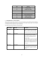
CONTENTS:
1. PREFACE--------------------------------------------------------------------------------------------------4
2. DESCRIPTION OF THE MODBUS PROTOCOL ------------------------------------------------4
2.1. ASCII framing---------------------------------------------------------------------------------------5
2.2. RTU framing ----------------------------------------------------------------------------------------5
2.3. Characteristic of frame fields -------------------------------------------------------------------6
2.4. LRC calculation ------------------------------------------------------------------------------------7
2.5. CRC calculation ------------------------------------------------------------------------------------7
2.6. Character formation during serial transmission --------------------------------------------8
2.7. Transaction interruption --------------------------------------------------------------------------8
3. FUNCTION DESCRIPTION ---------------------------------------------------------------------------8
3.1. Reading of N-registers (code 03) --------------------------------------------------------------8
3.2. Record of values into the register (code 06) ------------------------------------------------9
3.3. Record into N-registers (code 16) -------------------------------------------------------------9
3.4. Report identifying the device (code 17) ------------------------------------------------------10
4. ERROR CODES ------------------------------------------------------------------------------------------10
5. REGISTER MAP OF THE N10 METER ------------------------------------------------------------12
APPENDIX A – CALCULATION OF THE CHECKSUM---------------------------------------------20
3
1. PREFACE
The digital programmable N10 meter destined to measure parameters of power networks has been provided with
a serial interface in RS-485 standard to communicate with other devices.
The asynchronous communication protocol MODBUS has been implemented on this serial interface.
The configuration of serial interface parameters has been described in the Service Manual of the N10 meter.
Composition of serial interface parameters concerning N10 meter:
• Meter address
1...32
• Transmission speed
300/600/1200/2400/4800/9600/19,000 bits/sec
• Working modes
ASCII, RTU
• Information unit
ASCII: 8N1, 7E1, 701
RTU: 8N2, 8E1, 801
• Maximal response time
300 ms
Explanation of some abbreviations:
ASCII = American Standard Code for Information Interchange
RTU =
Remote Terminal Unit
LRC =
Longitudinal Redundancy Check
CRC = Cyclic Redundancy Check
CR =
Carriage Return
LF =
Line –Feed (Character)
MSB = Most – Significant Bit
2. DESCRIPTION OF THE MODBUS PROTOCOL
The MODBUS interface is a standard adopted by manufacturers of industrial controllers for an asynchronous
character exchange of information between different devices of measuring and controlling systems. It has the
following features:
• Simple access rule to the interface grounded on the „master slave” principle,
• Protection of transmitted messages against errors,
• Confirmation of remote order realisation and error signalling,
• Effective actions protecting against the system suspension,
• Taking advantage of the asynchronous character transmission.
Programmable controllers working in the MODBUS protocol can communicate with each other and with other
devices using the master – slave technique, in which only one device (the master) can initiate transactions (called
„queries”).
The other devices (the slaves) respond by supplying the requested data to the master, or by taking the action
requested in the query.
Typical master devices include host processors and programming pannels. Typical slaves include programmable
controllers. The master can address individual slaves, or can initiate a broadcast message to all slaves. Slaves
return a message called a „response” to queries that are addressed to them individually. (Responses are not
returned to broadcast queries from the master).
4
The MODBUS protocol establishes the format for the master’s query by placing into it the device address,
a function code defining the requested action, any data to be sent, and an error checking code.
The slave’s response message is also constructed using MODBUS protocol. It contains fields confirming the
action taken, any data to be returned, and an error checking code.
If an error occured in receipt of the message, or if the slave is unable to perform the requested action, the slave
will construct an error message and send it as its response.
At the message level, the MODBUS protocol still applies the master – slave principle even though the network
communication method is peer-to-peer. If a controller orginates a message it does so as a master device, and
expects a response from a slave device. Similarly, when a controller receives a message it constructs a slave
response and returns it to the originating controller.
The format of transmitted information is as follows:
•
Master ⇒ slave: device address, function code, data to be sent, error checking code
•
Slave ⇒ master: sender address, confirmation, data to be sent, error checking code
Devices working in the MODBUS protocol can be setup to communicate on standard MODBUS networks using
either of two transmission modes: ASCII or RTU. Users select the desired mode, along with the serial port
communication parameters (baud rate, parity mode, etc) during configuration of each controller.
The mode and serial parameters must be the same for all devices on a MODBUS network.
In the MODBUS system, transmitted messages are placed into frames that are not related to serial transmission.
These frames have a defined beginning and end. This enables for the receiving device to reject incomplete
frames and signalling of related errors with them.
Taking into consideration the possibility to operate in one of two different transmission modes (ASCII or RTU), two
frames have been defined.
2.1. ASCII framing
In the ASCII mode each byte of information is transmitted as two ASCII characters. The basic feature of this mode
is that it allows to long intervals between characters within the message (to 1 sec) without causing errors.
A typical message frame is shown below.
Start
Address
Function
Data
LRC
Check
End
Index
1 char
/:/
2 chars
2 chars
N chars
2 chars
2 chars
CR LF
In ASCII mode messages start with a colon ( : ) character („:”-ASCII 3Ahex) and end with a „carriage return – line
feed” (CR and LF characters). The frame information part is protected by the code LRC
(Longitudinal Redundancy Check).
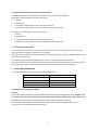
2.2. RTU Framing
In RTU mode, messages start with a silent interval of at least 3.5 character times.
This is most easily implemented as a multiple of character times at the baud rate that is being used on the
network.
5
The frame format is shown below:
Start
Address
Function
Data
CRC
Check
End
Index
T1-T2-T3-T4
8 bits
8 bits
N x 8bits
16 bits
T1-T2-T3-T4
Beginning and end indexes are marked symbolically as an interval equal to four lengths of the index (information
unit). The checking code consists of 16 bits and emerges as the result of CRC calculation (Cyclical Redundancy
Check) of the frame contents.
2.3. Characteristic of frame fields.
Address field
The address field of a message frame contains two characters (in ASCII mode) or eight bits (in RTU mode).
Valid slave device address are in the range of 0-247 decimal. The individual slave devices are assigned
addresses in the range of 0-247. The master addresses the slave unit by placing the slave address in the frame
address field. When the slave sends its response, it places its own address in this address field of the response to
let the master know which slave is responding. The address 0 is used as a broadcast address recognized by all
slave units connected to the bus.
Function field
The function code field of a message frame contains two characters (in ASCII mode) or eight bits (in RTU mode).
Valid codes are in the range of 1-255 decimal.
When a message is sent from a master to a slave device, the function code field tells the slave what kind of action
to perform. When the slave responds to the master, it uses the function code field to indicate either a normal
(error-free) response or that some kind of error occured (called an exception response). For a formal response
the slave simply echoes the original function code. For a formal response the slave returns a code that is
equivalent to the original function code with its most significant logic 1.
The error code is placed on the data field of the response frame.
Data field
The data field is constructed using sets of two hexadecimal digits, in the range of 00 to FF hexadecimal.
These can be made from a pair of ASCII characters or from one RTU character, according to the network’s serial
transmission mode.
The data field of messages sent from a master to slave devices contains additional information which the slave
must use to take the action defined by the function code. This can include items like discrete and register
addresses, the quantity of items to be handled, and count of actual data bytes in the field.
The data field can be non-existent (of zero length) in certain kinds of messages. For example, in a request from a
master device for a slave to respond with its communications event log (function code 0B hexdecimal) the slave
does not require any additional information. The function code alone specifies the action.
6
Error checking field
Two kinds of error-checking methods are used for standard MODBUS networks. The error checking field contents
depends upon the method that is being used.
ASCII
When ASCII mode is used for character framing, the error checking field contains two ASCII characters. The error
check characters are the result of a Longitudinal Redundancy Check (LRC) calculation that is performed on the
message contents, exclusive of the beginning „colon” and terminating CRLF characters. LRC characters are
appended to the message as the last field preceding the CRLF characters.
RTU
When RTU mode is used for character framing, the error checking field containts a 16-bit value implemented as
two 8-bit bytes. The error check value is the result of a Cyclical Redundancy Check calculation performed on a
message contents.
The CRC field is appended to the message as the last field in the message. When this is done, the low-order byte
of the field is appended first, followed by the high-order byte.
The CRC high-order byte is the last byte to be sent in the message.
2.4. LRC checking
The LRC is calculated by adding together sucessIve 8-bit bytes of the message, discarding any carries, and then
two is complementing the result. It is performed on the ASCII message field contents excluding the „colon”
character that begins the message, and excluding the CRLF pair at the end of the message.
The 8-bit value of the LRC sum is placed at the frame end as two ASCII characters, first the character containing
the older tetrad, and after it the character containing the younger LRC tetrad.
2.5. CRC checking
The generating procedure of CRC is realized according the following algorythm:
1.
Load a 16-bit register with FFFF hex. Call this the CRC register.
2.
Exclusive OR the first 8-bit byte of the message with the low-order byte of the 16 bit CRC register, putting the
result in the CRC register.
3.
Shift the CRC register one bit to the right (towards the LSB), zero-filling the MSB. Extract and examine the
4.
(If the LSB was 0): Repeat step 3 (another shift)
LSB.
(If the LSB was 1): Exclusive OR the CRC register with the polynomial value A001 hex.
5.
Repeats steps 3 and 4 until 8 shifts have been performed. When this is done, a complete 8-bit byte will have
been processed.
6.
Repeat steps 2 through 5 for the next 8-bit byte of the message. Continue doing this until all bytes have been
processed.
7.
The final contents of the CRC register is the CRC value.
8.
When the CRC is placed into the message, its upper and lower bytes must be swapped as described below.
7
2.6. Character formation during serial transmission
In the MODBUS protocol, characters are transmitted from the youngest to the oldest bit.
Organization of the information unit in the ASCII mode:
•
1 start bit,
•
7 data field bits,
•
1 even parity check bit (odd) or lack of even parity check bit,
•
1 stop bit at even parity check or 2 stop bits when lack of even parity check.
Organization of the information unit in the RTU mode:
•
1 start bit,
•
8 data field bits,
•
1 even parity check bit (odd) or lack of even parity check bit,
•
1 stop bit at even parity check or 2 stop bits when lack of even parity check.
2.7. Transaction interruption
In the master unit the user sets up the important parameter which is the „maximal response time on the query
frame” after which exceeding, the transaction is interrupted.
This time is choice such that each slave unit working in the system (even the slowest,) normally will have the time
to answer to the frame query.
An exceeding of this time attests therefore about an error and such is treated by the master unit.
If the unit slave will find out a transmission error it does not accomplish the order and does not send any answer.
That causes an exceeding of the waiting time after the query frame and the transaction interruption.
3. FUNCTION DESCRIPTION
In the N10 meter following protocol functions has been implemented:
Code
Signification
03
Reading of n-register
06
Record of an individual register
16
Record of n-registers
17
Slave device identification
3.1. Reading of n-registers (code 03)
Demand:
The function enables the reading of values included in registers in being addressed slave device. Registers are
16 or 32-bit units, which can include numerical values bounded with changeable processes, and the like.
The demand frame defines the 16-bit start address and the number of registers to read-out.
The signification of the register contents with address data can be different for different device types.
The function is not accessible in the broadcast mode.
8
Example: Reading of 3 registers beginning by the register with the 6Bhex address.
Address
Function
11
03
Register
Address
Register
Address
Hi
Lo
00
Number
of
Registers
Number
of
Registers
Hi
Lo
00
03
6B
Checking
sum
7E
LRC
Answer:
Register data are packing beginning from the smallest address: first the older byte, then the younger register byte.
Example: the answer frame
Address
Function
Number
Of
bites
Value
in the
register
107
Hi
11
03
06
02
Value
in the
register
107
Lo
Value
in the
register
108
Hi
Value
in the
register
108
Lo
Value
inthe
register
109
Hi
Value
in the
register
109
Lo
Checking
Sum
2B
00
00
00
64
55
LRC
3.2. Record of values in the register (code 06)
Demand:
The function enables the modification of the register contents.
It is accessible in the broadcast mode.
Example
Address
Function
Register
Address
Hi
Register
Address
Lo
Value
Hi
Value
Lo
Checking
sum
11
06
00
87
03
9E
C1
LRL
Answer:
The correct answer to a record requirement in the register is the retransmission of the message after
accomplishing the operation.
Example
Address
Function
Register
Address
Hi
Register
Address
Lo
Value
Hi
Value
Lo
Checking
sum
11
06
00
87
03
9E
C1
3.3. Record in n-registers (code 16)
Demand:
The function is accessible in broadcast mode. It enables the modification of the register contents.
9
LRC
Example: Record of two registers beginning from the register adressed 136.
Address
Function
Register
Address
Hi
Register
Address
Lo
Number
Of
registers
HI
Number
of registers
Lo
Number
of bytes
Data
Hi
Data
Lo
Data
Hi
Data
Lo
Checking
Sum
11
10
00
87
00
02
04
00
0A
01
02
45
LRC
Answer:
The correct answer includes the unit slave address, function code, starting address and the number of recorded
registers.
Example
Address
Function
Register
Address
Hi
Register
Address
Lo
Number
of
registers
Hi
Number
of
registers
Lo
Checking
sum
11
10
00
87
00
02
56
LRC
3.4. Report identifying the device (code 17)
Demand:
This function enables the user to obtain information about the device type, status and configuration depending on
this.
Example
Address
Function
Checking
Sum
11
11
DE
LRC
Answer:
The field „Device identificator” in the answer frame means the unique identificator of this class of device, however
the other fields include parameters depended on the device type.
Example concerning the N10 meter
Slave
address
Function
11
11
Byte
number
6
Device
identificator
Device
state
50
FF
Voltage
range
Current
sum
0064
0001
Checking
sum
4. ERROR CODES
When the master device is broadcasting a demand to the slave device then, except for messages in the
broadcast mode, it expects a correct answer. After sending the demand of the master unit one of the four
possibilities can occur:
•
If the slave unit receives the demand without a transmission error and can execute it correctly, then it returns
a correct answer,
10
•
If the slave unit does not receive the demand, no answer is returned. Timeout conditions for the demand will
be fulfilled in the master device programme.
•
If the slave unit receives the demand, but with transmission errors (even parity error of checking sum LRC or
CRC), no answer is returned. Timeout conditions for the demand will be fulfilled in the master device
programme.
•
If the slave unit receives the demand without a transmission error but does not execute it correctly (e.g. if the
demand is, the reading-out of a non-existent bit output or register), then it returns the answer including the
error code, informing the master device about the error reason.
•
A message with an incorrect answer includes two fields distinguishing it from the correct answer.
The function code field:
In the correct answer, the slave unit retransmits the function code from the demand message in the field of the
answer function code. All function codes have the most-significant bit (MSB) equal zero (code values are under
80h). In the incorrect answer, the slave unit sets up the MSB bit of the function code at 1.
This causes that the function code value in the incorrect answer is exactly plus 80h greater than it would be in a
correct answer.
On the base of the function code with a set up MSB bit the programme of the master device can recognize an
incorrect answer and can check the error code on the data field.
The data field:
In a correct answer the slave device can return data to the data field (certain information required by the master
unit). In the incorrect answer the slave unit returns the error code to the data field. It defines conditions of the
slave device which had produced the error.
An example considering a demand of a master device and the incorrect answer of the slave unit has been shown
below:
Example: demand
Slave
address
Function
Variable
Address
Hi
Variable
Address
Lo
Number
of
variables
Hi
Number
of
Variables
Lo
Checking
sum
0A
01
04
A1
00
01
4F
LRC
Example: incorrect answer
Slave
address
Function
Error
code
Checking
sum
0A
81
02
73
LRC
In this example the master device addresses the demand to the slave unit with No10 (0Ah). The function code
(01) serves to the read-out operation of the bit input state. Then this frame means the demand of the status readout of a one bit input with the address number: 1245 (04A1h).
If in the slave device there is no bit input with the given address, then the device returns the incorrect answer with
the No 02 error code. This means a forbidden data address in the slave device. Possible error codes and their
meanings are shown in the table below.
11
Code
Meaning
01
Forbidden function
02
Forbidden data address
03
Forbidden data value
04
Damage in the connected device
05
Confirmation
06
Occupied, message removed
07
Negative confirmation
08
Error of memory parity
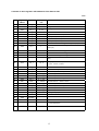
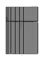
5. REGISTER MAP OF THE N10 METER
Data included in the N10 meter are located in 16-bit or 32-bit registers. Process variables and meter parameters
are placed in the register addresses area in a way depending on the variable value type. Bits in the 16-bit register
are numbered from the youngest to the oldest ones (b0-b15).
The register map has been devided into the following areas.
Address range
Value type
Description
4000 - 4031
Integer (16 bits)
The value is placed in one 16 bit register.
Table 1 includes the register description.
Registers can be read out and recorded.
7000 - 7223
Float (32 bits)
The value is placed in two successive
16-bit registers. Registers include these
same data as 32-bit registers from the
7500-7611 area.
Example: registers 7000 and 7001 include
the value from the register 7500, registers
7002 and 7003 include the value from the
register 7501, etc. Registers serves only
to read out.
7500 - 7779
Float (32 bits)
The value is placed in the 32-bit register.
The description of registers is included in
Table 2.
12
Contents of 16-bit registers with addresses from 4000 to 4031
Table 1
Item
Register
address
Symbol
Range
unit
1.
4000
Tr_I
1...20000
2.
4001
Tr_U
1...4000
3.
4002
Ao_n
0...34
4.
4003
Ao_L
80...120%
Coeficient rescaling the output
5.
4004
A0_0
0, 1
Range of the continuous output
6.
4005
Po_n
0.35...37
Quantity on the pulse output, code from Table 2
7.
4006
Po_c
0...9999
Constant of the pulse output
8.
4007
Pl_n
0; 38...40
9.
4008
Pl_c
1...9999
10.
4009
Pl_0
1
Cancellation of the external energy counter (counter of the
pulse input)
11.
4010
EnP0
1
Cancellation of the active energy counter
12.
4011
Enq0
1
Cancellation of the reactive energy counter
13.
4012
EnS0
1
Cancellation of the apparent energy counter
14.
4013
PA_0
1
Cancellation of the 15-minut active power Pav (max and min
value)
15.
4014
PA_t
1,2, 3
16.
4015
PA_S
0, 1
17.
4016
18.
4017
A1_n
0, 1...34
19.
4018
A1on
0...120 (%)
Two-state output 1 – switch on value
20.
4019
A1oF
0...120 (%)
Two-state output 1 – switch off value
21.
4020
A2_n
0, 1...34
Two-state output 2 – Quantity, code from Table 2
22.
4021
A2on
0...120(%)
Two-state output 2 – switch on value
23.
4022
A2oF
0...120(%)
Two-state output 2 – switch off value
24.
4023
A3_n
0, 1...34
Two-state output 3 – Quantity, code from Table 2
25.
4024
A3on
0...120(%)
Two-state output 3 – switch on value
26.
4025
A3oF
0...120(%)
Two-state output 3 – switch off value
27.
4026
AL._dt
0...100 sec.
Time-lag in relay operation
28.
4027
Year
1998-2083
Year
29.
4028
MonDay
Date in the format: month* 100 + day
30.
4029
HourMin
Time in the format: hour* 100 + minute
31.
4030
ALR
0...7
States of relay outputs:A1=bo, A2=b1, A3=b2
1 – output switched on
32.
4031
Harm
0, 1
The harmonic calculation mode is switched on.
0000...9999
Description
Current transformer ratio
Voltage transformer ration
Quantity on the continuous output, code from Table 2
Quantity on the pulse input, code from Table 2
Constant of the external energy counter (pulse input)
Averaging time of the Pav power
1-15 min., 2-30min., 3-60min
Synchronization of Pav power averaging with the real timer
Access code change
Two-state output 1 – Quantity, code from Table 2
13
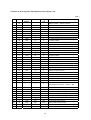
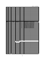
Contents of 32-bit registers with addresses from 7500 to 7779
Table 2
Item
Code
Register
address
Symbol
Range
unit
1
00
2
Description
01
7500
U1
V
L1 phase voltage
3
02
7501
I1
A
L1 phase current
4
03
7502
P1
W
L1 phase active power
5
04
7503
Q1
Var
L1 phase reactive power
6
05
7504
S1
VA
L1 phase apparent power
7
06
7505
Pf1
Pf
L1 phase active power factor
8
07
7506
tϕ1
tϕ
L1 phase reactive power over the active power
Without quantity – display extincted
9
08
7507
U2
V
L2 phase voltage
10
09
7508
I2
A
L2 phase current
11
10
7509
P2
W
L2 phase active power
12
11
7510
Q2
Var
L2 phase reactive power
13
12
7511
S2
VA
L2 phase apparent power
14
13
7512
Pf2
Pf
L2 phase active power factor
15
14
7513
tϕ2
tϕ
L2 phase reactive power over the active power
16
15
7514
U3
V
L3 phase voltage
17
16
7515
I3
A
L3 phase current
18
17
7516
P3
W
L3 phase active power
19
18
7517
Q3
Var
L3 phase reactive power
20
19
7518
S3
VA
L3 phase apparent power
21
20
7519
Pf3
Pf
L3 phase active power factor
22
21
7520
tϕ3
tϕ
L3 phase reactive power over the active power
23
22
7521
Us
V
Mean three-phase voltage
24
23
7522
Is
A
Mean three-phase current
25
24
7523
P
W
Three-phase active power
26
25
7524
Q
Var
Three-phase reactive power
27
26
7525
S
VA
Three-phase apparent power
28
27
7526
Pf
Pf
Active power factor
29
28
7527
tϕ
tϕ
Three-phase reactive power over the
three-phase active power – mean tϕ = Q/P
30
29
7528
f
Hy
Frequency
31
30
7529
U12
V
L1-L2 phase-to-phase voltage
32
31
7530
U23
V
L2-L3 phase-to-phase voltage
33
32
7531
U31
V
L3-L1 phase-to-phase voltage
34
33
7532
U123
V
Mean phase-to-phase voltage
35
34
7533
PAV
W
(e.g.) 15-minute mean active power
36
35
7534
EnP
Wh
Three-phase active energy
37
36
7535
Enb
VArh
Three-phase reactive energy
38
37
7536
EnS
Vah
Three-phase apparent energy
39
38
7537
EnPz
Wh
Active energy from an external counter
14
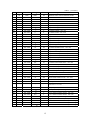
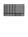
TABLE 2 (continuation)
40
38
7538
Enbz
VArh
Reactive energy from an external counter
41
40
7539
EnSz
VA
Apparent energy from an external counter
42
41
7540
Date – day, month
43
42
7541
Date-year
44
43
7542
Time- hours, minutes
45
44
7543
Time-secondes
46
7544, 7545
U1
V
L1 phase voltage – min, max
47
7546, 7547
U2
V
L2 phase voltage – min, max
48
7548, 7549
U3
V
L3 phase voltage – min, max
49
7550, 7551
I1
A
L1 phase current – min, max
50
7552, 7553
I2
A
L2 phase current – min, max
51
7554,7555
I3
A
L3 phase current – min, max
52
7556, 7557
P1
W
L1 phase active power – min, max
53
7558, 7559
P2
W
L2 phase active power – min, max
54
7560, 7561
P3
W
L3 phase active power – min, max
55
7562, 7563
S1
VA
L1 phase apparent power – min, max
56
7564, 7565
S2
VA
L2 phase apparent power – min, max
57
7566, 7567
S3
VA
L3 phase apparent power – min, max
58
7568, 7569
Q1
VAr
L1 phase reactive power – min, max
59
7570, 7571
Q2
VAr
L2 phase reactive power – min, max
60
7572, 7573
Q3
VAr
L3 phase reactive power – min, max
61
7574, 7575
Pf1
Pf
L1 phase active power factor – min, max
62
7576, 7577
Pf2
Pf
L2 phase active power factor – min, max
63
7578, 7579
Pf3
Pf
L3 phase active power factor – min, max
64
7580, 7581
tϕ1
tϕ1 = Q1/P1, L1 phase – min, max
65
7582, 7583
tϕ2
tϕ2 = Q2/P2, L2 phase – min, max
66
7584, 7585
tϕ3
67
7586, 7587
US
V
Mean three-phase voltage – min, max
68
7588, 7589
IS
A
Mean three-phase current – min, max
69
7590, 7591
P
W
Three-phase active power – min, max
70
7592, 7593
Q
VAr
Three-phase reactive power – min, max
71
7594, 7595
S
VA
Three-phase apparent power – min, max
72
7596, 7597
Pf
Pf
Active power factor – min, max
73
7598, 7599
tϕ
tϕ
Mean three-phase reactive power factor over active
power factor – min, max
74
7600, 7601
f
Hz
Frequency – min, max
75
7602, 7603
U12
V
L1-L2 phase-to-phase voltage - min, max
76
7604, 7605
U23
V
L2-L3 phase-to-phase voltage - min, max
77
7606, 7607
U31
V
L3-L1 phase-to-phase voltage - min, max
78
7608, 7609
U123
V
Mean phase-to-phase voltage - min, max
79
7610, 7611
PAV
W
(e.g.) 15 minute mean active power ) - min, max
tϕ3 = Q3/P3, L3 phase – min, max
80
45
7612
THDU1
%
Relative harmonic content of L1 phase voltage
81
46
7613
THDU2
%
Relative harmonic content of L2 phase voltage
82
47
7614
THDU3
%
Relative harmonic content of L3 phase voltage
15
TABLE 2 (continuation)
83
48
7615
THDI1
%
Relative harmonic content of L1 phase current
84
49
7616
THDI2
%
Relative harmonic content of L2 phase current
85
50
7617
THDI3
%
Relative harmonic content of L3 phase current
86
7618, 7619
THDU1
%
87
7620, 7621
THDU2
%
88
7622, 7623
THDU3
%
89
7624, 7625
THDI1
%
90
7626, 7627
THDI2
%
91
7628, 7629
THDI3
%
92
7630
HarU1[1]
%
Relative harmonic content of L1 phase
voltage – min,max
Relative harmonic content of L2 phase
voltage – min,max
Relative harmonic content of L3 phase
voltage – min,max
Relative harmonic content of L1 phase
current – min,max
Relative harmonic content of L2 phase
current – min,max
Relative harmonic content of L3 phase
current – min,max
1st harmonic of L1 phase voltage
93
7631
HarU1[2]
%
2nd harmonic of L1 phase voltage
94
7632
HarU1[3]
%
3rd harmonic of L1 phase voltage
95
7633
HarU1[4]
%
4th harmonic of L1 phase voltage
96
7634
HarU1[5]
%
5th harmonic of L1 phase voltage
97
7635
HarU1[6]
%
6th harmonic of L1 phase voltage
98
7636
HarU1[7]
%
7th harmonic of L1 phase voltage
99
7637
HarU1[8]
%
8th harmonic of L1 phase voltage
100
7638
HarU1[9]
%
9th harmonic of L1 phase voltage
101
7639
HarU1[10]
%
10th harmonic of L1 phase voltage
102
7640
HarU1[11]
%
11th harmonic of L1 phase voltage
103
7641
HarU1[12]
%
12th harmonic of L1 phase voltage
104
7642
HarU1[13]
%
13th harmonic of L1 phase voltage
105
7643
HarU1[14]
%
14th harmonic of L1 phase voltage
106
7644
HarU1[15]
%
15th harmonic of L1 phase voltage
107
7645
HarU1[16]
%
16th harmonic of L1 phase voltage
108
7646
HarU1[17]
%
17th harmonic of L1 phase voltage
109
7647
HarU1[18]
%
18th harmonic of L1 phase voltage
110
7648
HarU1[19]
%
19th harmonic of L1 phase voltage
111
7649
HarU1[20]
%
20th harmonic of L1 phase voltage
112
7650
HarU1[21]
%
21st harmonic of L1 phase voltage
113
7651
HarU1[22]
%
22nd harmonic of L1 phase voltage
114
7652
HarU1[23]
%
23rd harmonic of L1 phase voltage
115
7653
HarU1[24]
%
24th harmonic of L1 phase voltage
116
7654
HarU1[25]
%
25th harmonic of L1 phase voltage
117
7655
HarU2[1]
%
1st harmonic of L2 phase voltage
118
7656
HarU2[2]
%
2nd harmonic of L2 phase voltage
119
7657
HarU2[3]
%
3rd harmonic of L2 phase voltage
120
7658
HarU2[4]
%
4th harmonic of L2 phase voltage
121
7659
HarU2[5]
%
5th harmonic of L2 phase voltage
122
7660
HarU2[6]
%
6th harmonic of L2 phase voltage
123
7661
HarU2[7]
%
7th harmonic of L2 phase voltage
124
7662
HarU2[8]
%
8th harmonic of L2 phase voltage
125
7663
HarU2[9]
%
9th harmonic of L2 phase voltage
126
7664
HarU2[10]
%
10th harmonic of L2 phase voltage
16
TABLE 2 (continuation)
127
7665
HarU2[11]
%
11th harmonic of L2 phase voltage
128
7666
HarU2[12]
%
12th harmonic of L2 phase voltage
129
7667
HarU2[13]
%
13th harmonic of L2 phase voltage
130
7668
HarU2[14]
%
14th harmonic of L2 phase voltage
131
7669
HarU2[15]
%
15th harmonic of L2 phase voltage
132
7670
HarU2[16]
%
16th harmonic of L2 phase voltage
133
7671
HarU2[17]
%
17th harmonic of L2 phase voltage
134
7672
HarU2[18]
%
18th harmonic of L2 phase voltage
135
7673
HarU2[19]
%
19th harmonic of L2 phase voltage
136
7674
HarU2[20]
%
20th harmonic of L2 phase voltage
137
7675
HarU2[21]
%
21st harmonic of L2 phase voltage
138
7676
HarU2[22]
%
22nd harmonic of L2 phase voltage
139
7677
HarU2[23]
%
23rd harmonic of L2 phase voltage
140
7678
HarU2[24]
%
24th harmonic of L2 phase voltage
141
7679
HarU2[25]
%
25th harmonic of L2 phase voltage
142
7680
HarU3[1]
%
1st harmonic of L3 phase voltage
143
7681
HarU3[2]
%
2nd harmonic of L3 phase voltage
144
7682
HarU3[3]
%
3rd harmonic of L3 phase voltage
145
7683
HarU3[4]
%
4th harmonic of L3 phase voltage
146
7684
HarU3[5]
%
5th harmonic of L3 phase voltage
147
7685
HarU3[6]
%
6th harmonic of L3 phase voltage
148
7686
HarU3[7]
%
7th harmonic of L3 phase voltage
149
7687
HarU3[8]
%
8th harmonic of L3 phase voltage
150
7688
HarU3[9]
%
9th harmonic of L3 phase voltage
151
7689
HarU3[10]
%
10th harmonic of L3 phase voltage
152
7690
HarU3[11]
%
11th harmonic of L3 phase voltage
153
7691
HarU3[12]
%
12th harmonic of L3 phase voltage
154
7692
HarU3[13]
%
13th harmonic of L3 phase voltage
155
7693
HarU3[14]
%
14th harmonic of L3 phase voltage
156
7694
HarU3[15]
%
15th harmonic of L3 phase voltage
157
7695
HarU3[16]
%
16th harmonic of L3 phase voltage
158
7696
HarU3[17]
%
17th harmonic of L3 phase voltage
159
7697
HarU3[18]
%
18th harmonic of L3 phase voltage
160
7698
HarU3[19]
%
19th harmonic of L3 phase voltage
161
7699
HarU3[20]
%
20th harmonic of L3 phase voltage
162
7700
HarU3[21]
%
21st harmonic of L3 phase voltage
163
7701
HarU3[22]
%
22nd harmonic of L3 phase voltage
164
7702
HarU3[23]
%
23rd harmonic of L3 phase voltage
165
7703
HarU3[24]
%
24th harmonic of L3 phase voltage
166
7704
HarU3[25]
%
25th harmonic of L3 phase voltage
167
7705
HarI1[1]
%
1st harmonic of L1 phase current
168
7706
HarI1[2]
%
2nd harmonic of L1 phase current
169
7707
HarI1[3]
%
3rd harmonic of L1 phase current
170
7708
HarI1[4]
%
4th harmonic of L1 phase current
171
7709
HarI1[5]
%
5th harmonic of L1 phase current
172
7710
HarI1[6]
%
6th harmonic of L1 phase current
173
7711
HarI1[7]
%
7th harmonic of L1 phase current
174
7712
HarI1[8]
%
8th harmonic of L1 phase current
17
TABLE 2 (continuation)
175
7713
HarI1[9]
%
9th harmonic of L1 phase current
176
7714
HarI1[10]
%
10th harmonic of L1 phase current
177
7715
HarI1[11]
%
11th harmonic of L1 phase current
178
7716
HarI1[12]
%
12th harmonic of L1 phase current
179
7717
HarI1[13]
%
13th harmonic of L1 phase current
180
7718
HarI1[14]
%
14th harmonic of L1 phase current
181
7719
HarI1[15]
%
15th harmonic of L1 phase current
182
7720
HarI1[16]
%
16th harmonic of L1 phase current
183
7721
HarI1[17]
%
17th harmonic of L1 phase current
184
7722
HarI1[18]
%
18th harmonic of L1 phase current
185
7723
HarI1[19]
%
19th harmonic of L1 phase current
186
7724
HarI1[20]
%
20th harmonic of L1 phase current
187
7725
HarI1[21]
%
21st harmonic of L1 phase current
188
7726
HarI1[22]
%
22nd harmonic of L1 phase current
189
7727
HarI1[23]
%
23rd harmonic of L1 phase current
190
7728
HarI1[24]
%
24th harmonic of L1 phase current
191
7729
HarI1[25]
%
25th harmonic of L1 phase current
192
7730
HarI2[1]
%
1st harmonic of L2 phase current
193
7731
HarI2[2]
%
2nd harmonic of L2 phase current
194
7732
HarI2[3]
%
3rd harmonic of L2 phase current
195
7733
HarI2[4]
%
4th harmonic of L2 phase current
196
7734
HarI2[5]
%
5th harmonic of L2 phase current
197
7735
HarI2[6]
%
6th harmonic of L2 phase current
198
7736
HarI2[7]
%
7th harmonic of L2 phase current
199
7737
HarI2[8]
%
8th harmonic of L2 phase current
200
7738
HarI2[9]
%
9th harmonic of L2 phase current
201
7739
HarI2[10]
%
10th harmonic of L2 phase current
202
7740
HarI2[11]
%
11th harmonic of L2 phase current
203
7741
HarI2[12]
%
12th harmonic of L2 phase current
204
7742
HarI2[13]
%
13th harmonic of L2 phase current
205
7743
HarI2[14]
%
14th harmonic of L2 phase current
206
7744
HarI2[15]
%
15th harmonic of L2 phase current
207
7745
HarI2[16]
%
16th harmonic of L2 phase current
208
7746
HarI2[17]
%
17th harmonic of L2 phase current
209
7747
HarI2[18]
%
18th harmonic of L2 phase current
210
7748
HarI2[19]
%
19th harmonic of L2 phase current
211
7749
HarI2[20]
%
20th harmonic of L2 phase current
212
7750
HarI2[21]
%
21st harmonic of L2 phase current
213
7751
HarI2[22]
%
22nd harmonic of L2 phase current
214
7752
HarI2[23]
%
23rd harmonic of L2 phase current
215
7753
HarI2[24]
%
24th harmonic of L2 phase current
216
7754
HarI2[25]
%
25th harmonic of L2 phase current
217
7755
HarI3[1]
%
1st harmonic of L3 phase current
218
7756
HarI3[2]
%
2nd harmonic of L3 phase current
219
7757
HarI3[3]
%
3rd harmonic of L3 phase current
220
7758
HarI3[4]
%
4th harmonic of L3 phase current
221
7759
HarI3[5]
%
5th harmonic of L3 phase current
222
7760
HarI3[6]
%
6th harmonic of L3 phase current
18
TABLE 2 (continuation)
223
7761
HarI3[7]
%
7th harmonic of L3 phase current
224
7762
HarI3[8]
%
8th harmonic of L3 phase current
225
7763
HarI3[9]
%
9th harmonic of L3 phase current
226
7764
HarI3[10]
%
10th harmonic of L3 phase current
227
7765
HarI3[11]
%
11th harmonic of L3 phase current
228
7766
HarI3[12]
%
12th harmonic of L3 phase current
229
7767
HarI3[13]
%
13th harmonic of L3 phase current
230
7768
HarI3[14]
%
14th harmonic of L3 phase current
231
7769
HarI3[15]
%
15th harmonic of L3 phase current
232
7770
HarI3[16]
%
16th harmonic of L3 phase current
233
7771
HarI3[17]
%
17th harmonic of L3 phase current
234
7772
HarI3[18]
%
18th harmonic of L3 phase current
235
7773
HarI3[19]
%
19th harmonic of L3 phase current
236
7774
HarI3[20]
%
20th harmonic of L3 phase current
237
7775
HarI3[21]
%
21st harmonic of L3 phase current
238
7776
HarI3[22]
%
22nd harmonic of L3 phase current
239
7777
HarI3[23]
%
23rd harmonic of L3 phase current
240
7778
HarI3[24]
%
24th harmonic of L3 phase current
241
7779
HarI3[25]
%
25th harmonic of L3 phase current
19
APPENDIX A
CALCULATION OF THE CHECKING SUM
In this appendix some examples of function in the C language for calculate the LRC checking sum for ASCII
mode and the CRC checking sum for the RTU mode have been shown.
The function for LRC calculation has two arguments:
unsigned char* outMSg;
•
Index for the communication buffer, including binary data
from which one should calculate LRC.
unsigned short usDataLen;
•
Number of bytes in the communication buffer.
The function returns LRC of unsigned chart type.
static unsigned charLRC (outMsg, usDataLen)
unsigned char* outMsg
/* buffer to calculate LRC*/
unsigned short usDataLen;
/* number of bytes in the buffer*/
{
/*LRC unitialization*/
unsigned char uchLRC = 0
while (usDataLen- -)
uchLRC +=*outMsg++;
/* add the buffer byte without transfer*/
return ((unsigned char) (-(char uchLRC)));
/* return the sum in the completion code up two */
}
An example of function in C language calculating the CRC sum is presented below.
All possible values of CRC sum are placed in two tables.
The first table includes the oldest byte of all 256 possible values of the 16-bit CRC field, however the second table
includes the youngest byte.
The assignment of the CRC sum through tabel indexing is further more rapid than the calculation of a new CRC
value for each sign of the communication buffer.
Note: The below function represents bytes of the sum CRC older/younger, and this way the CRC value returned
by the function can be directly placed in the communication buffer.
The function serving to calculate CRC has two arguments:
unsigned char* puchMsg
Index for the communication buffer including
binary data from which one should calculate LRC.
unsigned short usDataLen;
Number of bytes in the communication buffer.
The function returns CRC of unsigned short type.
unsigned short CRC16 (puchMsg, usDataLen)
unsigned char* puchMsg;
/* Buffer to calculate CRC*/
unsigned short usDataLen
/* Number of bytes in the buffer*/
{
unsigned char uchCRChi = 0xFF
/*Initialization of the older CRC byte*/
unsigned char uchCRCIo = 0xFF
/*Initialization of the younger CRC byte*/
20
while (usDataLen--)
{
uIndex =
uchCRChi ^ *puchMsg++;
uchCRChi = uchCRClo ^ crc_hi[uIndex];
uchCRClo = crc_lo[uIndex];
}
return(uchCRChi<<8 | uchCRClo);
/* CRC calculation*/
}
//older CRC byte table/
const unsigned char crc_hi[ ]={
0x00,
0x40,
0x80,
0xC0,
0x00,
0x40,
0x80,
0xC0,
0x00,
0x40,
0x80,
0xC0,
0x00,
0x40,
0x80,
0xC0,
0x00,
0x40
};
0xC1,
0x01,
0x41,
0x80,
0xC1,
0x01,
0x41,
0x80,
0xC1,
0x00,
0x41,
0x80,
0xC1,
0x01,
0x41,
0x80,
0xC1,
0x81,
0xC0,
0x01,
0x41,
0x81,
0xC0,
0x00,
0x41,
0x81,
0xC1,
0x01,
0x41,
0x81,
0xC0,
0x00,
0x41,
0x81,
0x40,
0x80,
0xC0,
0x00,
0x40,
0x80,
0xC1,
0x00,
0x40,
0x81,
0xC0,
0x01,
0x40,
0x80,
0xC1,
0x00,
0x40,
0x01,
0x41,
0x80,
0xC1,
0x01,
0x41,
0x81,
0xC1,
0x01,
0x40,
0x80,
0xC0,
0x00,
0x41,
0x81,
0xC1,
0x01,
0xC0,
0x00,
0x41,
0x81,
0xC0,
0x00,
0x40,
0x81,
0xC0,
0x01,
0x41,
0x80,
0xC1,
0x01,
0x40,
0x81,
0xC0,
0x80,
0xC1,
0x00,
0x40,
0x80,
0xC1,
0x00,
0x40,
0x80,
0xC0,
0x00,
0x41,
0x81,
0xC0,
0x00,
0x40,
0x80,
0x41,
0x81,
0xC1,
0x01,
0x41,
0x81,
0xC1,
0x01,
0x41,
0x80,
0xC1,
0x00,
0x40,
0x80,
0xC1,
0x00,
0x41,
0x01,
0x40,
0x81,
0xC0,
0x00,
0x40,
0x81,
0xC0,
0x01,
0x41,
0x81,
0xC1,
0x01,
0x41,
0x81,
0xC1,
0x01,
0xC0,
0x00,
0x40,
0x80,
0xC1,
0x01,
0x40,
0x80,
0xC0,
0x00,
0x40,
0x81,
0xC0,
0x00,
0x40,
0x81,
0xC0,
0x80,
0xC1,
0x00,
0x41,
0x81,
0xC0,
0x01,
0x41,
0x80,
0xC1,
0x00,
0x40,
0x80,
0xC1,
0x01,
0x40,
0x80,
0x41,
0x81,
0xC1,
0x01,
0x40,
0x80,
0xC0,
0x00,
0x41,
0x81,
0xC1,
0x01,
0x41,
0x81,
0xC0,
0x01,
0x41,
0x00,
0x40,
0x81,
0xC0,
0x00,
0x41,
0x80,
0xC1,
0x00,
0x40,
0x81,
0xC0,
0x00,
0x40,
0x80,
0xC0,
0x00,
0xC1,
0x01,
0x40,
0x80,
0xC1,
0x01,
0x41,
0x81,
0xC1,
0x01,
0x40,
0x80,
0xC1,
0x01,
0x41,
0x80,
0xC1,
0x81,
0xC0,
0x01,
0x41,
0x81,
0xC0,
0x01,
0x40,
0x81,
0xC0,
0x01,
0x41,
0x81,
0xC0,
0x01,
0x41,
0x81,
0x03,
0x0F,
0xD9,
0xD5,
0x30,
0x3C,
0x38,
0xEC,
0x21,
0xA5,
0xAB,
0x7F,
0xB2,
0x96,
0x5E,
0x8A,
0x47,
0x02,
0xCF,
0x1B,
0x15,
0x31,
0xFC,
0x28,
0x2C,
0x20,
0x65,
0x69,
0xBF,
0xB3,
0x56,
0x5A,
0x4A,
0x46,
0xC2,
0xCE,
0xDB,
0xD7,
0xF1,
0xFD,
0xE8,
0xE4,
0xE0,
0x64,
0xA9,
0x7D,
0x73,
0x57,
0x9A,
0x4E,
0x86,
0xC6,
0x0E,
0xDA,
0x17,
0x33,
0x3D,
0xE9,
0x24,
0xA0,
0xA4,
0xA8,
0xBD,
0xB1,
0x97,
0x9B,
0x8E,
0x82,
0x06,
0x0A,
0x1A,
0x16,
0xF3,
0xFF,
0x29,
0x25,
0x60,
0x6C,
0x68,
0xBC,
0x71,
0x55,
0x5B,
0x8F,
0x42,
0x07,
0xCA,
0x1E,
0xD6,
0xF2,
0x3F,
0xEB,
0xE5,
0x61,
0xAC,
0x78,
0x7C,
0x70,
0x95,
0x99,
0x4F,
0x43,
0xC7,
0xCB,
0xDE,
0xD2,
0x32,
0x3E,
0x2B,
0x27,
0xA1,
0xAD,
0xB8,
0xB4,
0xB0,
0x94,
0x59,
0x8D,
0x83,
0x05,
0x0B,
0xDF,
0x12,
0x36,
0xFE,
0x2A,
0xE7,
0x63,
0x6D,
0xB9,
0x74,
0x50,
0x54,
0x58,
0x4D,
0x41,
0xC5,
0xC9,
0x1F,
0x13,
0xF6,
0xFA,
0xEA,
0xE6,
0xA3,
0xAF,
0x79,
0x75,
0x90,
0x9C,
0x98,
0x4C,
0x81,
0xC4,
0x09,
0xDD,
0xD3,
0xF7,
0x3A,
0xEE,
0x26,
0xA2,
0x6F,
0xBB,
0xB5,
0x91,
0x5C,
0x88,
0x8C,
0x80,
//younger CRC byte table/
const unsigned char crc_lo[ ]={
0x00,
0x04,
0x08,
0x1D,
0x11,
0x37,
0x3B,
0x2E,
0x22,
0x62,
0x6E,
0x7B,
0x77,
0x51,
0x5D,
0x48,
0x44,
0x40
0xC0,
0xCC,
0xC8,
0x1C,
0xD1,
0xF5,
0xFB,
0x2F,
0xE2,
0x66,
0xAE,
0x7A,
0xB7,
0x93,
0x9D,
0x49,
0x84,
0xC1,
0x0C,
0xD8,
0xDC,
0xD0,
0x35,
0x39,
0xEF,
0xE3,
0xA6,
0xAA,
0xBA,
0xB6,
0x53,
0x5F,
0x89,
0x85,
0x01,
0x0D,
0x18,
0x14,
0x10,
0x34,
0xF9,
0x2D,
0x23,
0xA7,
0x6A,
0xBE,
0x76,
0x52,
0x9F,
0x4B,
0x45,
0xC3,
0xCD,
0x19,
0xD4,
0xF0,
0xF4,
0xF8,
0xED,
0xE1,
0x67,
0x6B,
0x7E,
0x72,
0x92,
0x9E,
0x8B,
0x87,
};
21