1
RocketIO™
Transceiver
User Guide
UG024 (v2.2) November 7, 2003
R
R
"Xilinx" and the Xilinx logo shown above are registered trademarks of Xilinx, Inc. Any rights not expressly granted herein are reserved.
CoolRunner, RocketChips, Rocket IP, Spartan, StateBENCH, StateCAD, Virtex, XACT, XC2064, XC3090, XC4005, and XC5210 are
registered trademarks of Xilinx, Inc.
The shadow X shown above is a trademark of Xilinx, Inc.
ACE Controller, ACE Flash, A.K.A. Speed, Alliance Series, AllianceCORE, Bencher, ChipScope, Configurable Logic Cell, CORE Generator,
CoreLINX, Dual Block, EZTag, Fast CLK, Fast CONNECT, Fast FLASH, FastMap, Fast Zero Power, Foundation, Gigabit Speeds...and
Beyond!, HardWire, HDL Bencher, IRL, J Drive, JBits, LCA, LogiBLOX, Logic Cell, LogiCORE, LogicProfessor, MicroBlaze, MicroVia,
MultiLINX, NanoBlaze, PicoBlaze, PLUSASM, PowerGuide, PowerMaze, QPro, Real-PCI, RocketIO, SelectIO, SelectRAM, SelectRAM+,
Silicon Xpresso, Smartguide, Smart-IP, SmartSearch, SMARTswitch, System ACE, Testbench In A Minute, TrueMap, UIM, VectorMaze,
VersaBlock, VersaRing, Virtex-II Pro, Virtex-II EasyPath, Wave Table, WebFITTER, WebPACK, WebPOWERED, XABEL, XACTFloorplanner, XACT-Performance, XACTstep Advanced, XACTstep Foundry, XAM, XAPP, X-BLOX +, XC designated products, XChecker,
XDM, XEPLD, Xilinx Foundation Series, Xilinx XDTV, Xinfo, XSI, XtremeDSP and ZERO+ are trademarks of Xilinx, Inc.
The Programmable Logic Company is a service mark of Xilinx, Inc.
All other trademarks are the property of their respective owners.
Xilinx, Inc. does not assume any liability arising out of the application or use of any product described or shown herein; nor does it convey
any license under its patents, copyrights, or maskwork rights or any rights of others. Xilinx, Inc. reserves the right to make changes, at any
time, in order to improve reliability, function or design and to supply the best product possible. Xilinx, Inc. will not assume responsibility for
the use of any circuitry described herein other than circuitry entirely embodied in its products. Xilinx provides any design, code, or
information shown or described herein "as is." By providing the design, code, or information as one possible implementation of a feature,
application, or standard, Xilinx makes no representation that such implementation is free from any claims of infringement. You are
responsible for obtaining any rights you may require for your implementation. Xilinx expressly disclaims any warranty whatsoever with
respect to the adequacy of any such implementation, including but not limited to any warranties or representations that the implementation
is free from claims of infringement, as well as any implied warranties of merchantability or fitness for a particular purpose. Xilinx, Inc. devices
and products are protected under U.S. Patents. Other U.S. and foreign patents pending. Xilinx, Inc. does not represent that devices shown
or products described herein are free from patent infringement or from any other third party right. Xilinx, Inc. assumes no obligation to
correct any errors contained herein or to advise any user of this text of any correction if such be made. Xilinx, Inc. will not assume any liability
for the accuracy or correctness of any engineering or software support or assistance provided to a user.
Xilinx products are not intended for use in life support appliances, devices, or systems. Use of a Xilinx product in such applications without
the written consent of the appropriate Xilinx officer is prohibited.
The contents of this manual are owned and copyrighted by Xilinx. Copyright 1994-2003 Xilinx, Inc. All Rights Reserved. Except as stated
herein, none of the material may be copied, reproduced, distributed, republished, downloaded, displayed, posted, or transmitted in any form
or by any means including, but not limited to, electronic, mechanical, photocopying, recording, or otherwise, without the prior written consent
of Xilinx. Any unauthorized use of any material contained in this manual may violate copyright laws, trademark laws, the laws of privacy and
publicity, and communications regulations and statutes.
RocketIO™ Transceiver User Guide
www.xilinx.com
1-800-255-7778
UG024 (v2.2) November 7, 2003
RocketIO™ Transceiver User Guide
UG024 (v2.2) November 7, 2003
The following table shows the revision history for this document..
Date
Version
Revision
11/20/01
1.0
• Initial Xilinx release.
01/23/02
1.1
• Updated for typographical and other errors found during review.
02/25/02
1.2
• Part of Virtex-II Pro™ Developer’s Kit (March 2002 Release)
07/11/02
1.3
• Updated “PCB Design Requirements”. Added Appendix A, “RocketIO Transceiver
Timing Model.” Changed Cell Models to Appendix B.
09/27/02
1.4
• Added additional IMPORTANT NOTE regarding ISE revisions at the beginning of
Chapter 1
• Added material in section “CRC (Cyclic Redundancy Check).”
• Added section “Other Important Design Notes.”
• New pre-emphasis eye diagrams in section “Pre-emphasis Techniques.”
• Numerous parameter additions previously shown as “TBD” in “MGT Package Pins.”
10/16/02
1.5
• Corrected pinouts for FF1152 package, device column 2VP20/30, LOC Constraints
rows GT_X0_Y0 and GT_X0_Y1.
• Corrected section “CRC Latency” and Table 2-20 to express latency in terms of
TXUSRCLK and RXUSRCLK cycles.
• Corrected sequence of packet elements in Figure 2-30.
11/20/02
1.6
•
•
•
•
•
•
•
•
•
•
•
12/12/02
1.6.1
03/25/03
2.0
Table 1-2: Added support for XAUI Fibre Channel.
Corrected max PCB drive distance to 40 inches.
Reorganized content sequence in Chapter 2, “Digital Design Considerations.”
Table 1-5: Additional information in RXCOMMADET definition.
Code corrections in VHDL Clock templates.
“Data Path Latency” section expanded and reformatted.
Corrections in clocking scheme drawings. Addition of drawings showing clocking
schemes without using DCM.
Table B-1: Corrections in Valid Data Characters.
Table 3-4: Data added.
Corrections made to power regulator schematic, Figure 3-6.
Table 2-23: Data added/corrected.
• Added clarifying text regarding trace length vs. width.
•
•
•
•
Reorganized existing content
Added new content
Added Appendix C, “Related Online Documents”
Added “Index”
UG024 (v2.2) November 7, 2003
www.xilinx.com
1-800-255-7778
RocketIO™ Transceiver User Guide
Date
Version
Revision
06/12/03
2.1
• Table 1-2: Added qualifying footnote to XAUI 10GFC.
• Table 1-5: Corrected definition of RXRECCLK.
• Section “RocketIO Transceiver Instantiations” in Chapter 1: added text briefly
explaining what the Instantiation Wizard does.
• Table 2-14: Changed numerics from exact values to rounded-off approximations
(nearest 5,000), and added footnote calling attention to this.
• Section “Clocking” in Chapter 2: added text recommending use of an IBUFGDS for
reference clock input to FPGA fabric.
• Section “RXRECCLK” in Chapter 2: Deleted references to SERDES_10B attribute and
to divide-by-10. (RXRECCLK is always 1/20th the data rate.).
• Section “CRC_FORMAT” in Chapter 2: Corrected minimum data length for
USER_MODE to “greater than 20”.
• Table 3-5: Clarified the significance of the VTTX/VTRX voltages shown in this table.
• Section “AC and DC Coupling” in Chapter 3: Explanatory material added regarding
VTRX/VTTX settings when AC or DC coupling is used.
• Table 4-1: Corrected pinouts for FG256 and FG456.
• Table 4-3: Corrected pinouts for FF1517 (XC2VP70).
11/07/03
2.2
• Section “Clock Signals” in Chapter 2: Added material that states:
♦ the reference clock must be provided at all times.
♦ any added jitter on the reference clock will be reflected on the RX/TX I/O.
• Figure 2-3: Added a BUFG after the IBUFGDS reference clock buffer.
• Section “RX_BUFFER_USE” in Chapter 2: Corrected erroneous “USRCLK2” to
“RXUSRCLK/RXUSRCLK2”.
• Table 2-20: Added footnotes qualifying the maximum receive-side latency parameters
given in the table.
• Section “FIBRE_CHAN” in Chapter 2: Added specification for minimum data length
(24 bytes not including CRC placeholder).
• Section “ETHERNET” in Chapter 2: Added note indicating that Gigabit Ethernet 802.3
frame specifications must be adhered to.
• Table 2-23: Corrected “External” to “Internal” loopback. Improved explanation of
Parallel Mode loopback.
• Added Figure 2-28, “Serial and Parallel Loopback Logic.”
• Section “Clock and Data Recovery” in Chapter 3: Corrected text to make clear that
RXRECCLK is always 1/20th the incoming data rate, and that CDR requires a
minimum number of transitions to achieve and maintain a lock on the received data.
• Section “Voltage Regulation” in Chapter 3: Added material defining voltage regulator
requirements when a device other than the LT1963 is used.
• Section “AC and DC Coupling” in Chapter 3: Added footnote to Table 3-6 clarifying
VTRX/VTTX voltage compliance.
• Figure 3-17 and section “Epson EG-2121CA 2.5V (LVPECL Outputs)” in Chapter 3:
Added material specifying the optional use of an LVPECL buffer as an alternative to
the LVDS buffer previously specified.
• Table 4-2: Added pinouts for FG676 package, XC2VP20 and XC2VP30.
• Table A-5: Added BREFCLK parameters TBREFPWH and TBREFPWL.
• Section “Application Notes” in Appendix C: Included new Xilinx Application Notes
XAPP648, XAPP669, and XAPP670.
• Various non-technical edits and corrections.
RocketIO™ Transceiver User Guide
www.xilinx.com
1-800-255-7778
UG024 (v2.2) November 7, 2003
Table of Contents
Schedule of Figures . . . . . . . . . . . . . . . . . . . . . . . . . . . . . . . . . . . . . . . . . . . . . . . . . . . . . . . . .
11
Schedule of Tables . . . . . . . . . . . . . . . . . . . . . . . . . . . . . . . . . . . . . . . . . . . . . . . . . . . . . . . . . .
13
Preface: About This Guide
RocketIO Features . . . . . . . . . . . . . . . . . . . . . . . . . . . . . . . . . . . . . . . . . . . . . . . . . . . . . . . . . .
Guide Contents . . . . . . . . . . . . . . . . . . . . . . . . . . . . . . . . . . . . . . . . . . . . . . . . . . . . . . . . . . . . .
For More Information . . . . . . . . . . . . . . . . . . . . . . . . . . . . . . . . . . . . . . . . . . . . . . . . . . . . . . .
Additional Resources . . . . . . . . . . . . . . . . . . . . . . . . . . . . . . . . . . . . . . . . . . . . . . . . . . . . . . .
Conventions . . . . . . . . . . . . . . . . . . . . . . . . . . . . . . . . . . . . . . . . . . . . . . . . . . . . . . . . . . . . . . . .
15
15
16
16
17
Port and Attribute Names. . . . . . . . . . . . . . . . . . . . . . . . . . . . . . . . . . . . . . . . . . . . . . . . . . 17
Typographical . . . . . . . . . . . . . . . . . . . . . . . . . . . . . . . . . . . . . . . . . . . . . . . . . . . . . . . . . . . . 17
Online Document . . . . . . . . . . . . . . . . . . . . . . . . . . . . . . . . . . . . . . . . . . . . . . . . . . . . . . . . . 18
Chapter 1: RocketIO Transceiver Overview
Basic Architecture and Capabilities . . . . . . . . . . . . . . . . . . . . . . . . . . . . . . . . . . . . . . . . . . 19
RocketIO Transceiver Instantiations . . . . . . . . . . . . . . . . . . . . . . . . . . . . . . . . . . . . . . . . . 21
HDL Code Examples . . . . . . . . . . . . . . . . . . . . . . . . . . . . . . . . . . . . . . . . . . . . . . . . . . . 21
List of Available Ports . . . . . . . . . . . . . . . . . . . . . . . . . . . . . . . . . . . . . . . . . . . . . . . . . . . . . . .
Primitive Attributes . . . . . . . . . . . . . . . . . . . . . . . . . . . . . . . . . . . . . . . . . . . . . . . . . . . . . . . . .
Modifiable Primitives . . . . . . . . . . . . . . . . . . . . . . . . . . . . . . . . . . . . . . . . . . . . . . . . . . . . . . .
Byte Mapping . . . . . . . . . . . . . . . . . . . . . . . . . . . . . . . . . . . . . . . . . . . . . . . . . . . . . . . . . . . . . . .
22
26
31
35
Chapter 2: Digital Design Considerations
Clocking . . . . . . . . . . . . . . . . . . . . . . . . . . . . . . . . . . . . . . . . . . . . . . . . . . . . . . . . . . . . . . . . . . . . 37
Clock Signals . . . . . . . . . . . . . . . . . . . . . . . . . . . . . . . . . . . . . . . . . . . . . . . . . . . . . . . . . . . . .
BREFCLK . . . . . . . . . . . . . . . . . . . . . . . . . . . . . . . . . . . . . . . . . . . . . . . . . . . . . . . . . . . .
Clock Ratio . . . . . . . . . . . . . . . . . . . . . . . . . . . . . . . . . . . . . . . . . . . . . . . . . . . . . . . . . . . . . .
Digital Clock Manager (DCM) Examples . . . . . . . . . . . . . . . . . . . . . . . . . . . . . . . . . . . . .
Example 1a: Two-Byte Clock with DCM . . . . . . . . . . . . . . . . . . . . . . . . . . . . . . . . . . . .
Example 1b: Two-Byte Clock without DCM . . . . . . . . . . . . . . . . . . . . . . . . . . . . . . . . . .
Example 2: Four-Byte Clock . . . . . . . . . . . . . . . . . . . . . . . . . . . . . . . . . . . . . . . . . . . . . .
Example 3: One-Byte Clock. . . . . . . . . . . . . . . . . . . . . . . . . . . . . . . . . . . . . . . . . . . . . . .
Half-Rate Clocking Scheme . . . . . . . . . . . . . . . . . . . . . . . . . . . . . . . . . . . . . . . . . . . . . . . .
Multiplexed Clocking Scheme with DCM . . . . . . . . . . . . . . . . . . . . . . . . . . . . . . . . . . . .
Multiplexed Clocking Scheme without DCM . . . . . . . . . . . . . . . . . . . . . . . . . . . . . . . . .
RXRECCLK . . . . . . . . . . . . . . . . . . . . . . . . . . . . . . . . . . . . . . . . . . . . . . . . . . . . . . . . . . . . . .
Clock Dependency . . . . . . . . . . . . . . . . . . . . . . . . . . . . . . . . . . . . . . . . . . . . . . . . . . . . . . . .
Data Path Latency . . . . . . . . . . . . . . . . . . . . . . . . . . . . . . . . . . . . . . . . . . . . . . . . . . . . . . . .
37
38
40
40
41
44
44
48
52
53
53
54
54
54
Reset/Power Down . . . . . . . . . . . . . . . . . . . . . . . . . . . . . . . . . . . . . . . . . . . . . . . . . . . . . . . . . . 55
8B/10B Encoding/Decoding . . . . . . . . . . . . . . . . . . . . . . . . . . . . . . . . . . . . . . . . . . . . . . . . . . 58
Overview . . . . . . . . . . . . . . . . . . . . . . . . . . . . . . . . . . . . . . . . . . . . . . . . . . . . . . . . . . . . . . . . 58
8B/10B Encoder . . . . . . . . . . . . . . . . . . . . . . . . . . . . . . . . . . . . . . . . . . . . . . . . . . . . . . . 58
RocketIO™ Transceiver User Guide
UG024 (v2.2) November 7, 2003
www.xilinx.com
1-800-255-7778
5
R
8B/10B Decoder . . . . . . . . . . . . . . . . . . . . . . . . . . . . . . . . . . . . . . . . . . . . . . . . . . . . . . . 58
Ports and Attributes . . . . . . . . . . . . . . . . . . . . . . . . . . . . . . . . . . . . . . . . . . . . . . . . . . . . . . . 59
TXBYPASS8B10B,
RX_DECODE_USE . . . . . . . . . . . . . . . . . . . . . . . . . . . . . . . . . . . . . . . . . . . . . . . . . . . . .
TXCHARDISPVAL,
TXCHARDISPMODE . . . . . . . . . . . . . . . . . . . . . . . . . . . . . . . . . . . . . . . . . . . . . . . . . . .
TXCHARISK . . . . . . . . . . . . . . . . . . . . . . . . . . . . . . . . . . . . . . . . . . . . . . . . . . . . . . . . . .
TXRUNDISP . . . . . . . . . . . . . . . . . . . . . . . . . . . . . . . . . . . . . . . . . . . . . . . . . . . . . . . . . .
TXKERR . . . . . . . . . . . . . . . . . . . . . . . . . . . . . . . . . . . . . . . . . . . . . . . . . . . . . . . . . . . . .
RXCHARISK,
RXRUNDISP . . . . . . . . . . . . . . . . . . . . . . . . . . . . . . . . . . . . . . . . . . . . . . . . . . . . . . . . . .
RXDISPERR . . . . . . . . . . . . . . . . . . . . . . . . . . . . . . . . . . . . . . . . . . . . . . . . . . . . . . . . . .
RXNOTINTABLE . . . . . . . . . . . . . . . . . . . . . . . . . . . . . . . . . . . . . . . . . . . . . . . . . . . . . .
Vitesse Disparity Example . . . . . . . . . . . . . . . . . . . . . . . . . . . . . . . . . . . . . . . . . . . . . . . . .
Transmitting Vitesse Channel Bonding Sequence . . . . . . . . . . . . . . . . . . . . . . . . . . . . .
Receiving Vitesse Channel Bonding Sequence . . . . . . . . . . . . . . . . . . . . . . . . . . . . . . . .
8B/10B Bypass Serial Output . . . . . . . . . . . . . . . . . . . . . . . . . . . . . . . . . . . . . . . . . . . . . . .
8B/10B Serial Output Format . . . . . . . . . . . . . . . . . . . . . . . . . . . . . . . . . . . . . . . . . . . . . .
HDL Code Examples: Transceiver Bypassing of 8B/10B Encoding. . . . . . . . . . . . . . .
59
60
61
61
61
61
62
62
62
62
63
63
64
64
SERDES Alignment . . . . . . . . . . . . . . . . . . . . . . . . . . . . . . . . . . . . . . . . . . . . . . . . . . . . . . . . . 65
Overview . . . . . . . . . . . . . . . . . . . . . . . . . . . . . . . . . . . . . . . . . . . . . . . . . . . . . . . . . . . . . . . .
Serializer . . . . . . . . . . . . . . . . . . . . . . . . . . . . . . . . . . . . . . . . . . . . . . . . . . . . . . . . . . . . .
Deserializer . . . . . . . . . . . . . . . . . . . . . . . . . . . . . . . . . . . . . . . . . . . . . . . . . . . . . . . . . . .
Ports and Attributes . . . . . . . . . . . . . . . . . . . . . . . . . . . . . . . . . . . . . . . . . . . . . . . . . . . . . . .
ALIGN_COMMA_MSB . . . . . . . . . . . . . . . . . . . . . . . . . . . . . . . . . . . . . . . . . . . . . . . . .
ENPCOMMAALIGN,
ENMCOMMAALIGN. . . . . . . . . . . . . . . . . . . . . . . . . . . . . . . . . . . . . . . . . . . . . . . . . . .
PCOMMA_DETECT,
MCOMMA_DETECT . . . . . . . . . . . . . . . . . . . . . . . . . . . . . . . . . . . . . . . . . . . . . . . . . . .
COMMA_10B_MASK,
PCOMMA_10B_VALUE,
MCOMMA_10B_VALUE . . . . . . . . . . . . . . . . . . . . . . . . . . . . . . . . . . . . . . . . . . . . . . . .
DEC_PCOMMA_DETECT,
DEC_MCOMMA_DETECT,
DEC_VALID_COMMA_ONLY . . . . . . . . . . . . . . . . . . . . . . . . . . . . . . . . . . . . . . . . . . .
RXREALIGN . . . . . . . . . . . . . . . . . . . . . . . . . . . . . . . . . . . . . . . . . . . . . . . . . . . . . . . . . .
RXCHARISCOMMA . . . . . . . . . . . . . . . . . . . . . . . . . . . . . . . . . . . . . . . . . . . . . . . . . . .
RXCOMMADET . . . . . . . . . . . . . . . . . . . . . . . . . . . . . . . . . . . . . . . . . . . . . . . . . . . . . . .
65
65
65
65
65
66
68
68
68
68
69
69
Clock Recovery . . . . . . . . . . . . . . . . . . . . . . . . . . . . . . . . . . . . . . . . . . . . . . . . . . . . . . . . . . . . . 69
Overview . . . . . . . . . . . . . . . . . . . . . . . . . . . . . . . . . . . . . . . . . . . . . . . . . . . . . . . . . . . . . . . .
Clock Synthesizer . . . . . . . . . . . . . . . . . . . . . . . . . . . . . . . . . . . . . . . . . . . . . . . . . . . . . .
Clock and Data Recovery . . . . . . . . . . . . . . . . . . . . . . . . . . . . . . . . . . . . . . . . . . . . . . . .
Clock Correction. . . . . . . . . . . . . . . . . . . . . . . . . . . . . . . . . . . . . . . . . . . . . . . . . . . . . . . . . .
Ports and Attributes . . . . . . . . . . . . . . . . . . . . . . . . . . . . . . . . . . . . . . . . . . . . . . . . . . . . . . .
CLK_CORRECT_USE . . . . . . . . . . . . . . . . . . . . . . . . . . . . . . . . . . . . . . . . . . . . . . . . . . .
RX_BUFFER_USE . . . . . . . . . . . . . . . . . . . . . . . . . . . . . . . . . . . . . . . . . . . . . . . . . . . . . .
CLK_COR_SEQ_*_* . . . . . . . . . . . . . . . . . . . . . . . . . . . . . . . . . . . . . . . . . . . . . . . . . . . .
CLK_COR_SEQ_LEN . . . . . . . . . . . . . . . . . . . . . . . . . . . . . . . . . . . . . . . . . . . . . . . . . . .
69
69
70
70
71
71
72
72
72
CLK_COR_INSERT_IDLE_FLAG,
CLK_COR_KEEP_IDLE,
CLK_COR_REPEAT_WAIT . . . . . . . . . . . . . . . . . . . . . . . . . . . . . . . . . . . . . . . . . . . . . . 73
Synchronization Logic . . . . . . . . . . . . . . . . . . . . . . . . . . . . . . . . . . . . . . . . . . . . . . . . . . . . . . 74
Overview . . . . . . . . . . . . . . . . . . . . . . . . . . . . . . . . . . . . . . . . . . . . . . . . . . . . . . . . . . . . . . . . 74
6
www.xilinx.com
1-800-255-7778
RocketIO™ Transceiver User Guide
UG024 (v2.2) November 7, 2003
R
Ports and Attributes . . . . . . . . . . . . . . . . . . . . . . . . . . . . . . . . . . . . . . . . . . . . . . . . . . . . . . . 74
RXCLKCORCNT . . . . . . . . . . . . . . . . . . . . . . . . . . . . . . . . . . . . . . . . . . . . . . . . . . . . . . 74
RX_LOS_INVALID_INCR,
RX_LOS_THRESHOLD . . . . . . . . . . . . . . . . . . . . . . . . . . . . . . . . . . . . . . . . . . . . . . . . . 75
RX_LOSS_OF_SYNC_FSM . . . . . . . . . . . . . . . . . . . . . . . . . . . . . . . . . . . . . . . . . . . . . . . 75
RXLOSSOFSYNC . . . . . . . . . . . . . . . . . . . . . . . . . . . . . . . . . . . . . . . . . . . . . . . . . . . . . . 75
Channel Bonding (Channel Alignment) . . . . . . . . . . . . . . . . . . . . . . . . . . . . . . . . . . . . . 76
Overview . . . . . . . . . . . . . . . . . . . . . . . . . . . . . . . . . . . . . . . . . . . . . . . . . . . . . . . . . . . . . . . .
Channel Bonding (Alignment) Operation . . . . . . . . . . . . . . . . . . . . . . . . . . . . . . . . . . . .
Ports and Attributes . . . . . . . . . . . . . . . . . . . . . . . . . . . . . . . . . . . . . . . . . . . . . . . . . . . . . . .
CHAN_BOND_MODE . . . . . . . . . . . . . . . . . . . . . . . . . . . . . . . . . . . . . . . . . . . . . . . . . .
ENCHANSYNC . . . . . . . . . . . . . . . . . . . . . . . . . . . . . . . . . . . . . . . . . . . . . . . . . . . . . . .
CHAN_BOND_ONE_SHOT. . . . . . . . . . . . . . . . . . . . . . . . . . . . . . . . . . . . . . . . . . . . . .
CHAN_BOND_SEQ_*_*,
CHAN_BOND__SEQ_LEN,
CHAN_BOND_SEQ_2_USE . . . . . . . . . . . . . . . . . . . . . . . . . . . . . . . . . . . . . . . . . . . . . .
CHAN_BOND_WAIT,
CHAN_BOND_OFFSET,
CHAN_BOND_LIMIT . . . . . . . . . . . . . . . . . . . . . . . . . . . . . . . . . . . . . . . . . . . . . . . . . .
CHBONDDONE . . . . . . . . . . . . . . . . . . . . . . . . . . . . . . . . . . . . . . . . . . . . . . . . . . . . . . .
CHBONDI,
CHBONDO . . . . . . . . . . . . . . . . . . . . . . . . . . . . . . . . . . . . . . . . . . . . . . . . . . . . . . . . . . .
RXCLKCORCNT,
RXLOSSOFSYNC . . . . . . . . . . . . . . . . . . . . . . . . . . . . . . . . . . . . . . . . . . . . . . . . . . . . . .
76
77
78
78
78
78
79
79
80
80
80
Troubleshooting . . . . . . . . . . . . . . . . . . . . . . . . . . . . . . . . . . . . . . . . . . . . . . . . . . . . . . . . . . 80
CRC (Cyclic Redundancy Check) . . . . . . . . . . . . . . . . . . . . . . . . . . . . . . . . . . . . . . . . . . . . 81
Overview . . . . . . . . . . . . . . . . . . . . . . . . . . . . . . . . . . . . . . . . . . . . . . . . . . . . . . . . . . . . . . . .
CRC Operation . . . . . . . . . . . . . . . . . . . . . . . . . . . . . . . . . . . . . . . . . . . . . . . . . . . . . . . .
CRC Generation . . . . . . . . . . . . . . . . . . . . . . . . . . . . . . . . . . . . . . . . . . . . . . . . . . . . . . .
CRC Latency . . . . . . . . . . . . . . . . . . . . . . . . . . . . . . . . . . . . . . . . . . . . . . . . . . . . . . . . . .
Ports and Attributes . . . . . . . . . . . . . . . . . . . . . . . . . . . . . . . . . . . . . . . . . . . . . . . . . . . . . . .
TX_CRC_USE,
RX_CRC_USE . . . . . . . . . . . . . . . . . . . . . . . . . . . . . . . . . . . . . . . . . . . . . . . . . . . . . . . . .
CRC_FORMAT . . . . . . . . . . . . . . . . . . . . . . . . . . . . . . . . . . . . . . . . . . . . . . . . . . . . . . . .
CRC_START_OF_PACKET,
CRC_END_OF_PACKET . . . . . . . . . . . . . . . . . . . . . . . . . . . . . . . . . . . . . . . . . . . . . . . .
RXCHECKINGCRC,
RXCRCERR . . . . . . . . . . . . . . . . . . . . . . . . . . . . . . . . . . . . . . . . . . . . . . . . . . . . . . . . . . .
TXFORCECRCERR,
TX_CRC_FORCE_VALUE . . . . . . . . . . . . . . . . . . . . . . . . . . . . . . . . . . . . . . . . . . . . . . .
81
81
81
81
82
82
82
85
85
85
RocketIO CRC Support Limitations . . . . . . . . . . . . . . . . . . . . . . . . . . . . . . . . . . . . . . . . . 85
Fabric Interface (Buffers) . . . . . . . . . . . . . . . . . . . . . . . . . . . . . . . . . . . . . . . . . . . . . . . . . . . . 86
Overview: Transmitter and Elastic (Receiver) Buffers . . . . . . . . . . . . . . . . . . . . . . . . . .
Transmitter Buffer (FIFO) . . . . . . . . . . . . . . . . . . . . . . . . . . . . . . . . . . . . . . . . . . . . . . . .
Receiver Buffer . . . . . . . . . . . . . . . . . . . . . . . . . . . . . . . . . . . . . . . . . . . . . . . . . . . . . . . .
Ports and Attributes . . . . . . . . . . . . . . . . . . . . . . . . . . . . . . . . . . . . . . . . . . . . . . . . . . . . . . .
TXBUFERR . . . . . . . . . . . . . . . . . . . . . . . . . . . . . . . . . . . . . . . . . . . . . . . . . . . . . . . . . . .
TX_BUFFER_USE . . . . . . . . . . . . . . . . . . . . . . . . . . . . . . . . . . . . . . . . . . . . . . . . . . . . . .
RXBUFSTATUS . . . . . . . . . . . . . . . . . . . . . . . . . . . . . . . . . . . . . . . . . . . . . . . . . . . . . . .
RX_BUFFER_USE . . . . . . . . . . . . . . . . . . . . . . . . . . . . . . . . . . . . . . . . . . . . . . . . . . . . . .
86
86
86
86
86
86
87
87
Miscellaneous Signals. . . . . . . . . . . . . . . . . . . . . . . . . . . . . . . . . . . . . . . . . . . . . . . . . . . . . . . 87
Ports and Attributes . . . . . . . . . . . . . . . . . . . . . . . . . . . . . . . . . . . . . . . . . . . . . . . . . . . . . . . 87
RocketIO™ Transceiver User Guide
UG024 (v2.2) November 7, 2003
www.xilinx.com
1-800-255-7778
7
R
RX_DATA_WIDTH,
TX_DATA_WIDTH . . . . . . . . . . . . . . . . . . . . . . . . . . . . . . . . . . . . . . . . . . . . . . . . . . . .
SERDES_10B . . . . . . . . . . . . . . . . . . . . . . . . . . . . . . . . . . . . . . . . . . . . . . . . . . . . . . . . . .
TERMINATION_IMP . . . . . . . . . . . . . . . . . . . . . . . . . . . . . . . . . . . . . . . . . . . . . . . . . . .
TXPOLARITY,
RXPOLARITY,
TXINHIBIT . . . . . . . . . . . . . . . . . . . . . . . . . . . . . . . . . . . . . . . . . . . . . . . . . . . . . . . . . . .
TX_DIFF_CTRL,
PRE_EMPHASIS . . . . . . . . . . . . . . . . . . . . . . . . . . . . . . . . . . . . . . . . . . . . . . . . . . . . . . .
LOOPBACK . . . . . . . . . . . . . . . . . . . . . . . . . . . . . . . . . . . . . . . . . . . . . . . . . . . . . . . . . .
87
87
87
88
88
88
Other Important Design Notes . . . . . . . . . . . . . . . . . . . . . . . . . . . . . . . . . . . . . . . . . . . . . . 90
Receive Data Path 32-bit Alignment . . . . . . . . . . . . . . . . . . . . . . . . . . . . . . . . . . . . . . . . .
32-bit Alignment Design . . . . . . . . . . . . . . . . . . . . . . . . . . . . . . . . . . . . . . . . . . . . . . . . . . .
Verilog . . . . . . . . . . . . . . . . . . . . . . . . . . . . . . . . . . . . . . . . . . . . . . . . . . . . . . . . . . . . . .
VHDL . . . . . . . . . . . . . . . . . . . . . . . . . . . . . . . . . . . . . . . . . . . . . . . . . . . . . . . . . . . . . . .
90
91
91
94
Chapter 3: Analog Design Considerations
Serial I/O Description . . . . . . . . . . . . . . . . . . . . . . . . . . . . . . . . . . . . . . . . . . . . . . . . . . . . . . . 99
Pre-emphasis Techniques . . . . . . . . . . . . . . . . . . . . . . . . . . . . . . . . . . . . . . . . . . . . . . . . . . 100
Differential Receiver . . . . . . . . . . . . . . . . . . . . . . . . . . . . . . . . . . . . . . . . . . . . . . . . . . . . . . . 103
Jitter . . . . . . . . . . . . . . . . . . . . . . . . . . . . . . . . . . . . . . . . . . . . . . . . . . . . . . . . . . . . . . . . . . . . . . . 103
Clock and Data Recovery . . . . . . . . . . . . . . . . . . . . . . . . . . . . . . . . . . . . . . . . . . . . . . . . . . . 103
PCB Design Requirements . . . . . . . . . . . . . . . . . . . . . . . . . . . . . . . . . . . . . . . . . . . . . . . . . 104
Power Conditioning . . . . . . . . . . . . . . . . . . . . . . . . . . . . . . . . . . . . . . . . . . . . . . . . . . . . .
Voltage Regulation . . . . . . . . . . . . . . . . . . . . . . . . . . . . . . . . . . . . . . . . . . . . . . . . . . . .
Passive Filtering . . . . . . . . . . . . . . . . . . . . . . . . . . . . . . . . . . . . . . . . . . . . . . . . . . . . . .
High-Speed Serial Trace Design . . . . . . . . . . . . . . . . . . . . . . . . . . . . . . . . . . . . . . . . . . .
Routing Serial Traces . . . . . . . . . . . . . . . . . . . . . . . . . . . . . . . . . . . . . . . . . . . . . . . . . .
Differential Trace Design . . . . . . . . . . . . . . . . . . . . . . . . . . . . . . . . . . . . . . . . . . . . . . .
AC and DC Coupling . . . . . . . . . . . . . . . . . . . . . . . . . . . . . . . . . . . . . . . . . . . . . . . . . .
Reference Clock . . . . . . . . . . . . . . . . . . . . . . . . . . . . . . . . . . . . . . . . . . . . . . . . . . . . . . . . .
Epson EG-2121CA 2.5V (LVPECL Outputs) . . . . . . . . . . . . . . . . . . . . . . . . . . . . . . . . .
Pletronics LV1145B (LVDS Outputs) . . . . . . . . . . . . . . . . . . . . . . . . . . . . . . . . . . . . . .
104
105
106
109
109
109
111
112
112
112
Other Important Design Notes . . . . . . . . . . . . . . . . . . . . . . . . . . . . . . . . . . . . . . . . . . . . . 113
Powering the RocketIO Transceivers . . . . . . . . . . . . . . . . . . . . . . . . . . . . . . . . . . . . . . . 113
The POWERDOWN Port . . . . . . . . . . . . . . . . . . . . . . . . . . . . . . . . . . . . . . . . . . . . . . . . . 113
Chapter 4: Simulation and Implementation
Simulation Models . . . . . . . . . . . . . . . . . . . . . . . . . . . . . . . . . . . . . . . . . . . . . . . . . . . . . . . . . 115
SmartModels . . . . . . . . . . . . . . . . . . . . . . . . . . . . . . . . . . . . . . . . . . . . . . . . . . . . . . . . . . . . 115
HSPICE . . . . . . . . . . . . . . . . . . . . . . . . . . . . . . . . . . . . . . . . . . . . . . . . . . . . . . . . . . . . . . . . 115
Implementation Tools . . . . . . . . . . . . . . . . . . . . . . . . . . . . . . . . . . . . . . . . . . . . . . . . . . . . . . 115
Par. . . . . . . . . . . . . . . . . . . . . . . . . . . . . . . . . . . . . . . . . . . . . . . . . . . . . . . . . . . . . . . . . . . . . 115
MGT Package Pins . . . . . . . . . . . . . . . . . . . . . . . . . . . . . . . . . . . . . . . . . . . . . . . . . . . . . . . . . 117
Appendix A: RocketIO Transceiver Timing Model
Timing Parameters . . . . . . . . . . . . . . . . . . . . . . . . . . . . . . . . . . . . . . . . . . . . . . . . . . . . . . . . . 123
Setup/Hold Times of Inputs Relative to Clock . . . . . . . . . . . . . . . . . . . . . . . . . . . . . . . 123
Clock to Output Delays . . . . . . . . . . . . . . . . . . . . . . . . . . . . . . . . . . . . . . . . . . . . . . . . . . . 123
8
www.xilinx.com
1-800-255-7778
RocketIO™ Transceiver User Guide
UG024 (v2.2) November 7, 2003
R
Clock Pulse Width . . . . . . . . . . . . . . . . . . . . . . . . . . . . . . . . . . . . . . . . . . . . . . . . . . . . . . . 124
Timing Parameter Tables and Diagram . . . . . . . . . . . . . . . . . . . . . . . . . . . . . . . . . . . . . 124
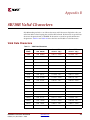
Appendix B: 8B/10B Valid Characters
Valid Data Characters . . . . . . . . . . . . . . . . . . . . . . . . . . . . . . . . . . . . . . . . . . . . . . . . . . . . . . 129
Valid Control Characters (K-Characters) . . . . . . . . . . . . . . . . . . . . . . . . . . . . . . . . . . . . 137
Appendix C: Related Online Documents
Application Notes . . . . . . . . . . . . . . . . . . . . . . . . . . . . . . . . . . . . . . . . . . . . . . . . . . . . . . . . . . 139
XAPP648: Serial Backplane Interface to a Shared Memory . . . . . . . . . . . . . . . . . . . . .
XAPP649: SONET Rate Conversion in Virtex-II Pro Devices . . . . . . . . . . . . . . . . . . .
XAPP651: SONET and OTN Scramblers/Descramblers . . . . . . . . . . . . . . . . . . . . . . .
XAPP652: Word Alignment and SONET/SDH Deframing . . . . . . . . . . . . . . . . . . . .
XAPP660: Partial Reconfiguration of RocketIO Pre-emphasis
and Differential Swing Control Attributes . . . . . . . . . . . . . . . . . . . . . . . . . . . . . . . .
XAPP661: RocketIO Transceiver Bit-Error Rate Tester . . . . . . . . . . . . . . . . . . . . . . . .
XAPP662: In-Circuit Partial Reconfiguration of RocketIO Attributes . . . . . . . . . . . .
XAPP669: PPC405 PPE Reference System Using Virtex-II Pro
RocketIO Transceivers . . . . . . . . . . . . . . . . . . . . . . . . . . . . . . . . . . . . . . . . . . . . . . . . .
XAPP670: Minimizing Receiver Elastic Buffer Delay in the Virtex-II Pro
RocketIO Transceiver . . . . . . . . . . . . . . . . . . . . . . . . . . . . . . . . . . . . . . . . . . . . . . . . . .
139
139
139
140
140
140
140
141
141
Characterization Reports . . . . . . . . . . . . . . . . . . . . . . . . . . . . . . . . . . . . . . . . . . . . . . . . . . . 141
Virtex-II Pro RocketIO Multi-Gigabit Transceiver
Characterization Summary . . . . . . . . . . . . . . . . . . . . . . . . . . . . . . . . . . . . . . . . . . . . . 141
Virtex-II Pro RocketIO MGT HSSDC2 Cable Characterization. . . . . . . . . . . . . . . . . . 142
White Papers . . . . . . . . . . . . . . . . . . . . . . . . . . . . . . . . . . . . . . . . . . . . . . . . . . . . . . . . . . . . . . . 142
WP157: Usage Models for Multi-Gigabit Serial Transceivers . . . . . . . . . . . . . . . . . . . 142
WP160: Emulating External SERDES Devices with
Embedded RocketIO Transceivers . . . . . . . . . . . . . . . . . . . . . . . . . . . . . . . . . . . . . . . 142
Index . . . . . . . . . . . . . . . . . . . . . . . . . . . . . . . . . . . . . . . . . . . . . . . . . . . . . . . . . . . . . . . . . . . . . . . . . . .
RocketIO™ Transceiver User Guide
UG024 (v2.2) November 7, 2003
www.xilinx.com
1-800-255-7778
143
9
R
10
www.xilinx.com
1-800-255-7778
RocketIO™ Transceiver User Guide
UG024 (v2.2) November 7, 2003
Schedule of Figures
Chapter 1: RocketIO Transceiver Overview
Figure 1-1: RocketIO Transceiver Block Diagram . . . . . . . . . . . . . . . . . . . . . . . . . . . . . . . . . 20
Chapter 2: Digital Design Considerations
Figure 2-1: REFCLK/BREFCLK Selection Logic . . . . . . . . . . . . . . . . . . . . . . . . . . . . . . . . . . . 39
Figure 2-2: Two-Byte Clock with DCM . . . . . . . . . . . . . . . . . . . . . . . . . . . . . . . . . . . . . . . . . . 41
Figure 2-3: Two-Byte Clock without DCM . . . . . . . . . . . . . . . . . . . . . . . . . . . . . . . . . . . . . . . 44
Figure 2-4: Four-Byte Clock . . . . . . . . . . . . . . . . . . . . . . . . . . . . . . . . . . . . . . . . . . . . . . . . . . . . 44
Figure 2-5: One-Byte Clock. . . . . . . . . . . . . . . . . . . . . . . . . . . . . . . . . . . . . . . . . . . . . . . . . . . . . 48
Figure 2-6: One-Byte Data Path Clocks, SERDES_10B = TRUE . . . . . . . . . . . . . . . . . . . . . 52
Figure 2-7: Two-Byte Data Path Clocks, SERDES_10B = TRUE . . . . . . . . . . . . . . . . . . . . . 52
Figure 2-8: Four-Byte Data Path Clocks, SERDES_10B = TRUE . . . . . . . . . . . . . . . . . . . . . 52
Figure 2-9: Multiplexed REFCLK with DCM . . . . . . . . . . . . . . . . . . . . . . . . . . . . . . . . . . . . . 53
Figure 2-10: Multiplexed REFCLK without DCM . . . . . . . . . . . . . . . . . . . . . . . . . . . . . . . . . 53
Figure 2-11: Using RXRECCLK to Generate RXUSRCLK and RXUSRCLK2. . . . . . . . . . 54
Figure 2-12: 8B/10B Data Flow . . . . . . . . . . . . . . . . . . . . . . . . . . . . . . . . . . . . . . . . . . . . . . . . . . 59
Figure 2-13: 10-Bit TX Data Map with 8B/10B Bypassed . . . . . . . . . . . . . . . . . . . . . . . . . . . 63
Figure 2-14: 10-Bit RX Data Map with 8B/10B Bypassed . . . . . . . . . . . . . . . . . . . . . . . . . . . 63
Figure 2-15: 8B/10B Parallel to Serial Conversion . . . . . . . . . . . . . . . . . . . . . . . . . . . . . . . . . 64
Figure 2-16: 4-Byte Serial Structure. . . . . . . . . . . . . . . . . . . . . . . . . . . . . . . . . . . . . . . . . . . . . . 64
Figure 2-17: Synchronizing Comma Align Signals to RXRECCLK . . . . . . . . . . . . . . . . . . 66
Figure 2-18: Top MGT Comma Control Flip-Flop Ideal Locations . . . . . . . . . . . . . . . . . . 67
Figure 2-19: Bottom MGT Comma Control Flip-Flop Ideal Locations . . . . . . . . . . . . . . . 67
Figure 2-20: Clock Correction in Receiver . . . . . . . . . . . . . . . . . . . . . . . . . . . . . . . . . . . . . . . . 70
Figure 2-21: RXLOSSOFSYNC FSM States . . . . . . . . . . . . . . . . . . . . . . . . . . . . . . . . . . . . . . . 75
Figure 2-22: Channel Bonding (Alignment) . . . . . . . . . . . . . . . . . . . . . . . . . . . . . . . . . . . . . . 76
Figure 2-23: CRC Packet Format . . . . . . . . . . . . . . . . . . . . . . . . . . . . . . . . . . . . . . . . . . . . . . . . 81
Figure 2-24: USER_MODE / FIBRE_CHAN Mode . . . . . . . . . . . . . . . . . . . . . . . . . . . . . . . . 83
Figure 2-25: Ethernet Mode . . . . . . . . . . . . . . . . . . . . . . . . . . . . . . . . . . . . . . . . . . . . . . . . . . . . 83
Figure 2-26: Infiniband Mode . . . . . . . . . . . . . . . . . . . . . . . . . . . . . . . . . . . . . . . . . . . . . . . . . . 84
Figure 2-27: Local Route Header . . . . . . . . . . . . . . . . . . . . . . . . . . . . . . . . . . . . . . . . . . . . . . . . 85
Figure 2-28: Serial and Parallel Loopback Logic . . . . . . . . . . . . . . . . . . . . . . . . . . . . . . . . . . 89
Figure 2-29: RXDATA Aligned Correctly . . . . . . . . . . . . . . . . . . . . . . . . . . . . . . . . . . . . . . . . 90
Figure 2-30: Realignment of RXDATA. . . . . . . . . . . . . . . . . . . . . . . . . . . . . . . . . . . . . . . . . . . 91
Chapter 3: Analog Design Considerations
Figure 3-1: Differential Amplifier. . . . . . . . . . . . . . . . . . . . . . . . . . . . . . . . . . . . . . . . . . . . . . . 99
Figure 3-2: Alternating K28.5+ with No Pre-Emphasis . . . . . . . . . . . . . . . . . . . . . . . . . . . . 101
RocketIO™ Transceiver User Guide
UG024 (v2.2) November 7, 2003
www.xilinx.com
1-800-255-7778
11
R
Figure 3-3: K28.5+ with Pre-Emphasis . . . . . . . . . . . . . . . . . . . . . . . . . . . . . . . . . . . . . . . . . . 101
Figure 3-4: Eye Diagram, 10% Pre-Emphasis, 20" FR4, Worst-Case Conditions . . . . . . 102
Figure 3-5: Eye Diagram, 33% Pre-Emphasis, 20" FR4, Worst-Case Conditions . . . . . . 102
Figure 3-6: Power Supply Circuit Using LT1963 Regulator . . . . . . . . . . . . . . . . . . . . . . . . 105
Figure 3-7: Power Filtering Network for One Transceiver. . . . . . . . . . . . . . . . . . . . . . . . . 106
Figure 3-8: Example Power Filtering PCB Layout for Four MGTs, Top Layer. . . . . . . . 107
Figure 3-9: Example Power Filtering PCB Layout for Four MGTs, Bottom Layer. . . . . 107
Figure 3-10: Example Power Filtering PCB Layout for Eight MGTs, Top Layer . . . . . . 108
Figure 3-11: Example Power Filtering PCB Layout for Eight MGTs, Bottom Layer . . . 108
Figure 3-12: Single-Ended Trace Geometry. . . . . . . . . . . . . . . . . . . . . . . . . . . . . . . . . . . . . . 110
Figure 3-13: Microstrip Edge-Coupled Differential Pair . . . . . . . . . . . . . . . . . . . . . . . . . . 110
Figure 3-14: Stripline Edge-Coupled Differential Pair . . . . . . . . . . . . . . . . . . . . . . . . . . . . 110
Figure 3-15: AC-Coupled Serial Link . . . . . . . . . . . . . . . . . . . . . . . . . . . . . . . . . . . . . . . . . . . 111
Figure 3-16: DC-Coupled Serial Link . . . . . . . . . . . . . . . . . . . . . . . . . . . . . . . . . . . . . . . . . . . 111
Figure 3-17: LVPECL Reference Clock Oscillator Interface. . . . . . . . . . . . . . . . . . . . . . . . 112
Figure 3-18: LVPECL Reference Clock Oscillator Interface (On-Chip Termination) . . 112
Figure 3-19: LVDS Reference Clock Oscillator Interface . . . . . . . . . . . . . . . . . . . . . . . . . . 112
Figure 3-20: LVDS Reference Clock Oscillator Interface (On-Chip Termination) . . . . 112
Chapter 4: Simulation and Implementation
Figure 4-1: 2VP2 Implementation . . . . . . . . . . . . . . . . . . . . . . . . . . . . . . . . . . . . . . . . . . . . . . 116
Figure 4-2: 2VP50 Implementation . . . . . . . . . . . . . . . . . . . . . . . . . . . . . . . . . . . . . . . . . . . . . 116
Appendix A: RocketIO Transceiver Timing Model
Figure A-1: RocketIO Transceiver Block Diagram . . . . . . . . . . . . . . . . . . . . . . . . . . . . . . . 122
Figure A-2: RocketIO Transceiver Timing Relative to Clock Edge . . . . . . . . . . . . . . . . . 127
Appendix B: 8B/10B Valid Characters
Appendix C: Related Online Documents
12
www.xilinx.com
1-800-255-7778
RocketIO™ Transceiver User Guide
UG024 (v2.2) November 7, 2003
Schedule of Tables
Chapter 1: RocketIO Transceiver Overview
Table 1-1: Number of RocketIO Cores per Device Type . . . . . . . . . . . . . . . . . . . . . . . . . . . 19
Table 1-2: Communications Standards Supported by RocketIO Transceiver . . . . . . . . . 19
Table 1-3: Serial Baud Rates and the SERDES_10B Attribute . . . . . . . . . . . . . . . . . . . . . . . 20
Table 1-4: Supported RocketIO Transceiver Primitives . . . . . . . . . . . . . . . . . . . . . . . . . . . . 21
Table 1-5: GT_CUSTOM (1), GT_AURORA, GT_FIBRE_CHAN (2), GT_ETHERNET (2),
GT_INFINIBAND, and GT_XAUI Primitive Ports . . . . . . . . . . . . . . . . . . . . . . . . . . . . . 22
Table 1-6: RocketIO Transceiver Attributes . . . . . . . . . . . . . . . . . . . . . . . . . . . . . . . . . . . . . . 26
Table 1-7: Default Attribute Values: GT_AURORA, GT_CUSTOM, GT_ETHERNET . 31
Table 1-8: Default Attribute Values: GT_FIBRE_CHAN, GT_INFINIBAND,
and GT_XAUI . . . . . . . . . . . . . . . . . . . . . . . . . . . . . . . . . . . . . . . . . . . . . . . . . . . . . . . . . . . . . . 33
Table 1-9: Control/Status Bus Association to Data Bus Byte Paths. . . . . . . . . . . . . . . . . . . 35
Chapter 2: Digital Design Considerations
Table 2-1: Clock Ports. . . . . . . . . . . . . . . . . . . . . . . . . . . . . . . . . . . . . . . . . . . . . . . . . . . . . . . . . . 37
Table 2-2: Reference Clock Usage . . . . . . . . . . . . . . . . . . . . . . . . . . . . . . . . . . . . . . . . . . . . . . . 38
Table 2-3: BREFCLK Pin Numbers . . . . . . . . . . . . . . . . . . . . . . . . . . . . . . . . . . . . . . . . . . . . . . 39
Table 2-4: Data Width Clock Ratios . . . . . . . . . . . . . . . . . . . . . . . . . . . . . . . . . . . . . . . . . . . . . 40
Table 2-5: DCM Outputs for Different DATA_WIDTHs . . . . . . . . . . . . . . . . . . . . . . . . . . 40
Table 2-6: Latency through Various Transmitter Components/Processes. . . . . . . . . . . . . 54
Table 2-7: Latency through Various Receiver Components/Processes. . . . . . . . . . . . . . . . 55
Table 2-8: Reset and Power Control Descriptions . . . . . . . . . . . . . . . . . . . . . . . . . . . . . . . . . 55
Table 2-9: Power Control Descriptions. . . . . . . . . . . . . . . . . . . . . . . . . . . . . . . . . . . . . . . . . . . 55
Table 2-10: 8B/10B Bypassed Signal Significance . . . . . . . . . . . . . . . . . . . . . . . . . . . . . . . . . 60
Table 2-11: Running Disparity Control . . . . . . . . . . . . . . . . . . . . . . . . . . . . . . . . . . . . . . . . . . 61
Table 2-12: Possible Locations of Comma Character . . . . . . . . . . . . . . . . . . . . . . . . . . . . . . . 66
Table 2-13: Effects of Comma-Related Ports and Attributes . . . . . . . . . . . . . . . . . . . . . . . . 69
Table 2-14: Data Bytes Allowed Between Clock Corrections as a Function of
REFCLK Stability and IDLE Sequences Removed . . . . . . . . . . . . . . . . . . . . . . . . . . . . . . 71
Table 2-15: Clock Correction Sequence / Data Correlation for 16-Bit Data Port . . . . . . . 72
Table 2-16: Applicable Clock Correction Sequences . . . . . . . . . . . . . . . . . . . . . . . . . . . . . . . 72
Table 2-17: RXCLKCORCNT Definition . . . . . . . . . . . . . . . . . . . . . . . . . . . . . . . . . . . . . . . . . 74
Table 2-18: Bonded Channel Connections . . . . . . . . . . . . . . . . . . . . . . . . . . . . . . . . . . . . . . . . 77
Table 2-19: Master/Slave Channel Bonding Attribute Settings. . . . . . . . . . . . . . . . . . . . . . 78
Table 2-20: Effects of CRC on Transceiver Latency (1) . . . . . . . . . . . . . . . . . . . . . . . . . . . . . . 82
Table 2-21: Global and Local Headers . . . . . . . . . . . . . . . . . . . . . . . . . . . . . . . . . . . . . . . . . . . 84
Table 2-22: Serial Speed Ranges as a Function of SERDES_10B. . . . . . . . . . . . . . . . . . . . . 87
Table 2-23: LOOPBACK Modes. . . . . . . . . . . . . . . . . . . . . . . . . . . . . . . . . . . . . . . . . . . . . . . . . 89
Table 2-24: 32-bit RXDATA, Aligned versus Misaligned. . . . . . . . . . . . . . . . . . . . . . . . . . . 90
RocketIO™ Transceiver User Guide
UG024 (v2.2) November 7, 2003
www.xilinx.com
1-800-255-7778
13
R
Chapter 3: Analog Design Considerations
Table 3-1: Differential Transmitter Parameters . . . . . . . . . . . . . . . . . . . . . . . . . . . . . . . . . . . 99
Table 3-2: Pre-emphasis Values . . . . . . . . . . . . . . . . . . . . . . . . . . . . . . . . . . . . . . . . . . . . . . . . 100
Table 3-3: Differential Receiver Parameters . . . . . . . . . . . . . . . . . . . . . . . . . . . . . . . . . . . . . 103
Table 3-4: CDR Parameters . . . . . . . . . . . . . . . . . . . . . . . . . . . . . . . . . . . . . . . . . . . . . . . . . . . . 104
Table 3-5: Transceiver Power Supplies . . . . . . . . . . . . . . . . . . . . . . . . . . . . . . . . . . . . . . . . . 105
Table 3-6: VTRX and VTTX for AC- and DC-Coupled Environments . . . . . . . . . . . . . . . . 111
Chapter 4: Simulation and Implementation
Table 4-1: LOC Grid & Package Pins Correlation for FG256/456 & FF672 . . . . . . . . . . . . . . . . . 117
Table 4-2: LOC Grid & Package Pins Correlation for FG676, FF896, and FF1152 . . . . . . . . . . . . 118
Table 4-3: LOC Grid & Package Pins Correlation for FF1517 and FF1704 . . . . . . . . . . . . . . . . . 119
Appendix A: RocketIO Transceiver Timing Model
Table A-1: RocketIO Clock Descriptions . . . . . . . . . . . . . . . . . . . . . . . . . . . . . . . . . . . . . . . . 121
Table A-2: Parameters Relative to the RX User Clock (RXUSRCLK) . . . . . . . . . . . . . . . . 124
Table A-3: Parameters Relative to the RX User Clock2 (RXUSRCLK2) . . . . . . . . . . . . . . 125
Table A-4: Parameters Relative to the TX User Clock2 (TXUSRCLK2) . . . . . . . . . . . . . . 125
Table A-5: Miscellaneous Clock Parameters . . . . . . . . . . . . . . . . . . . . . . . . . . . . . . . . . . . . . 126
Appendix B: 8B/10B Valid Characters
Table B-1: Valid Data Characters . . . . . . . . . . . . . . . . . . . . . . . . . . . . . . . . . . . . . . . . . . . . . . . 129
Table B-2: Valid Control Characters (K-Characters) . . . . . . . . . . . . . . . . . . . . . . . . . . . . . . 137
Appendix C: Related Online Documents
14
www.xilinx.com
1-800-255-7778
RocketIO™ Transceiver User Guide
UG024 (v2.2) November 7, 2003
R
Preface
About This Guide
The RocketIO Transceiver User Guide provides the product designer with the detailed
technical information needed to successfully implement the RocketIO™ multi-gigabit
transceiver in Virtex-II Pro Platform FPGA designs.
RocketIO Features
The RocketIO transceiver’s flexible, programmable features allow a multi-gigabit serial
transceiver to be easily integrated into any Virtex-II Pro design:
•
Variable-speed, full-duplex transceiver, allowing 600 Mbps to 3.125 Gbps baud
transfer rates
•
Monolithic clock synthesis and clock recovery system, eliminating the need for
external components
•
Automatic lock-to-reference function
•
Five levels of programmable serial output differential swing (800 mV to 1600 mV
peak-peak), allowing compatibility with other serial system voltage levels
•
Four levels of programmable pre-emphasis
•
AC and DC coupling
•
Programmable 50Ω/75Ω on-chip termination, eliminating the need for external
termination resistors
•
Serial and parallel TX-to-RX internal loopback modes for testing operability
•
Programmable comma detection to allow for any protocol and detection of any 10-bit
character.
Guide Contents
The RocketIO Transceiver User Guide contains these sections:
•
Preface, “About This Guide” — This section.
•
Chapter 1, “RocketIO Transceiver Overview” — An overview of the transceiver’s
capabilities and how it works.
•
Chapter 2, “Digital Design Considerations” — Ports and attributes for the six
provided communications protocol primitives; VHDL/Verilog code examples for
clocking and reset schemes; transceiver instantiation; 8B/10B encoding; CRC; channel
bonding.
•
Chapter 3, “Analog Design Considerations” — RocketIO serial overview; preemphasis; jitter; clock/data recovery; PCB design requirements.
RocketIO™ Transceiver User Guide
UG024 (v2.2) November 7, 2003
www.xilinx.com
1-800-255-7778
15
R
Preface: About This Guide
•
Chapter 4, “Simulation and Implementation” — Simulation models; implementation
tools; debugging and diagnostics.
•
Appendix A, “RocketIO Transceiver Timing Model” — Timing parameters associated
with the RocketIO transceiver core.
•
Appendix B, “8B/10B Valid Characters” — Valid data and K-characters.
•
Appendix C, “Related Online Documents” — Bibliography of online Application
Notes, Characterization Reports, and White Papers.
For More Information
For a complete menu of online information resources available on the Xilinx website, visit
http://www.xilinx.com/virtex2pro/ or refer to Appendix C, “Related Online
Documents.”
For a comprehensive listing of available tutorials and resources on network technologies
and communications protocols, visit http://www.iol.unh.edu/training/.
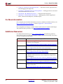
Additional Resources
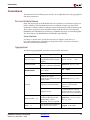
For additional information, go to http://support.xilinx.com. The following table lists
some of the resources you can access from this website. You can also directly access these
resources using the provided URLs.
Resource
Tutorials
Description/URL
Tutorials covering Xilinx design flows, from design entry to
verification and debugging
http://support.xilinx.com/support/techsup/tutorials/index.htm
Answer Browser
Database of Xilinx solution records
http://support.xilinx.com/xlnx/xil_ans_browser.jsp
Application Notes
Descriptions of device-specific design techniques and approaches
http://support.xilinx.com/apps/appsweb.htm
Data Sheets
Device-specific information on Xilinx device characteristics,
including readback, boundary scan, configuration, length count,
and debugging
http://support.xilinx.com/xlnx/xweb/xil_publications_index.jsp
Problem Solvers
Interactive tools that allow you to troubleshoot your design issues
http://support.xilinx.com/support/troubleshoot/psolvers.htm
Tech Tips
Latest news, design tips, and patch information for the Xilinx
design environment
http://www.support.xilinx.com/xlnx/xil_tt_home.jsp
16
www.xilinx.com
1-800-255-7778
RocketIO™ Transceiver User Guide
UG024 (v2.2) November 7, 2003
R
Conventions
Conventions
This document uses the following conventions. An example illustrates each typographical
and online convention.
Port and Attribute Names
Input and output ports of the RocketIO transceiver primitives are denoted in upper-case
letters. Attributes of the RocketIO transceiver are denoted in upper-case letters with
underscores. Trailing numbers in primitive names denote the byte width of the data path.
These values are preset and not modifiable. When assumed to be the same frequency,
RXUSRCLK and TXUSRCLK are referred to as USRCLK and can be used interchangeably.
This also holds true for RXUSRCLK2, TXUSRCLK2, and USRCLK2.
Comma Definition
A comma is a “K-character” used by the transceiver to align the serial data on a
byte/half-word boundary (depending on the protocol used), so that the serial data is
correctly decoded into parallel data.
Typographical
The following typographical conventions are used in this document:
Convention
Meaning or Use
Example
Courier font
Messages, prompts, and
program files that the system
displays
speed grade: - 100
Courier bold
Literal commands that you
enter in a syntactical statement
ngdbuild design_name
Commands that you select
from a menu
File → Open
Keyboard shortcuts
Ctrl+C
Variables in a syntax
statement for which you must
supply values
ngdbuild design_name
References to other manuals
See the Development System
Reference Guide for more
information.
Emphasis in text
If a wire is drawn so that it
overlaps the pin of a symbol,
the two nets are not connected.
An optional entry or
parameter. However, in bus
specifications, such as
bus[7:0], they are required.
ngdbuild [option_name]
design_name
A list of items from which you
must choose one or more
lowpwr ={on|off}
Helvetica bold
Italic font
Square brackets
Braces
RocketIO™ Transceiver User Guide
UG024 (v2.2) November 7, 2003
{ }
[ ]
www.xilinx.com
1-800-255-7778
17
R
Preface: About This Guide
Convention
Meaning or Use
Example
Separates items in a list of
choices
lowpwr ={on|off}
Vertical ellipsis
.
.
.
Repetitive material that has
been omitted
IOB #1: Name = QOUT’
IOB #2: Name = CLKIN’
.
.
.
Horizontal ellipsis . . .
Repetitive material that has
been omitted
allow block block_name
loc1 loc2 ... locn;
Vertical bar
|
Online Document
The following conventions are used in this document:
Convention
18
Meaning or Use
Example
See the section “Additional
Resources” for details.
Blue text
Cross-reference link to a
location in the current
document
Red text
Cross-reference link to a
location in another document
See Figure 2-5 in the Virtex-II
Handbook.
Blue, underlined text
Hyperlink to a website (URL)
Go to http://www.xilinx.com
for the latest speed files.
www.xilinx.com
1-800-255-7778
Refer to “Title Formats” in
Chapter 1 for details.
RocketIO™ Transceiver User Guide
UG024 (v2.2) November 7, 2003
R
Chapter 1
RocketIO Transceiver Overview
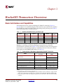
Basic Architecture and Capabilities
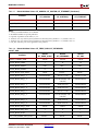
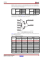
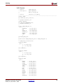
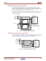
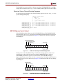
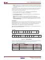
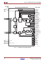
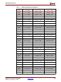
The RocketIO transceiver is based on Mindspeed’s SkyRail™ technology. Figure 1-1,
page 20, depicts an overall block diagram of the transceiver. Up to 24 transceiver modules
are available on a single Virtex-II Pro FPGA, depending on the part being used. Table 1-1
shows the RocketIO cores available by device.
Table 1-1:
Number of RocketIO Cores per Device Type
Device
RocketIO
Cores
Device
RocketIO
Cores
Device
RocketIO
Cores
XC2VP2
4
XC2VP30
8
XC2VP100
0 or 20
XC2VP4
4
XC2VP40
0 or 12
XC2VP125
0, 20, or 24
XC2VP7
8
XC2VP50
0 or 16
XC2VP20
8
XC2VP70
16 or 20
The transceiver module is designed to operate at any serial bit rate in the range of
600 Mbps to 3.125 Gbps per channel, including the specific bit rates used by the
communications standards listed in Table 1-2. The serial bit rate need not be configured in
the transceiver, as the operating frequency is implied by the received data, the reference
clock applied, and the SERDES_10B attribute (see Table 1-3).
Table 1-2:
Communications Standards Supported by RocketIO Transceiver
Channels
(Lanes) (1)
Mode
I/O Bit Rate
(Gbps)
1.06
Fibre Channel
1
Gbit Ethernet
1
1.25
4
3.125
4
3.1875 (3)
XAUI (10-Gbit Ethernet)
XAUI (10-Gbit Fibre
Channel) (2)
Infiniband
2.12
1, 4, 12
2.5
Aurora (Xilinx protocol)
1, 2, 3, 4, ...
0.600 – 3.125
Custom Mode
1, 2, 3, 4, ...
0.600 – 3.125
Notes:
1. One channel is considered to be one transceiver.
2. Supported with the GT_CUSTOM primitive. Certain attributes must be modified to comply with the
XAUI 10GFC specifications, including but not limited to CLK_COR_SEQ and CHAN_BOND_SEQ.
3. Bit rate is possible with the following topology specification: maximum 6" FR4 and one Molex 74441
connector.
RocketIO™ Transceiver User Guide
UG024 (v2.2) November 7, 2003
www.xilinx.com
1-800-255-7778
19
R
Chapter 1: RocketIO Transceiver Overview
Table 1-3:
SERDES_10B
Serial Baud Rate
FALSE
1.0 Gbps – 3.125 Gbps
TRUE
600 Mbps – 1.0 Gbps
PACKAGE
PINS
AVCCAUXRX
VTRX
Serial Baud Rates and the SERDES_10B Attribute
MULTI-GIGABIT TRANSCEIVER CORE
FPGA FABRIC
Power Down
2.5V RX
POWERDOWN
RXRECCLK
RXPOLARITY
RXREALIGN
RXCOMMADET
ENPCOMMAALIGN
ENMCOMMAALIGN
Termination Supply RX
CRC
Check
RXCHECKINGCRC
RXCRCERR
RXDATA[15:0]
RXDATA[31:16]
RXP
Comma
Detect
Realign
RXN
Clock
Manager
8B/10B
Decoder
RXNOTINTABLE[3:0]
RXDISPERR[3:0]
RXCHARISK[3:0]
RXCHARISCOMMA[3:0]
RXRUNDISP[3:0]
RXBUFSTATUS[1:0]
ENCHANSYNC
CHBONDDONE
CHBONDI[3:0]
CHBONDO[3:0]
Channel Bonding
and
Clock Correction
Parallel Loopback Path
Serial Loopback Path
Deserializer
RX
Elastic
Buffer
RXLOSSOFSYNC
RXCLKCORCNT
TXBUFERR
TXFORCECRCERR
TXDATA[15:0]
TXDATA[31:16]
TX
FIFO
TXP
TXN
Serializer
8B/10B
Encoder
CRC
Output
Polarity
TXBYPASS8B10B[3:0]
TXCHARISK[3:0]
TXCHARDISPMODE[3:0]
TXCHARDISPVAL[3:0]
TXKERR[3:0]
TXRUNDISP[3:0]
TXPOLARITY
TXINHIBIT
GNDA
AVCCAUXTX
VTTX
LOOPBACK[1:0]
TXRESET
RXRESET
REFCLK
REFCLK2
REFCLKSEL
BREFCLK
BREFCLK2
RXUSRCLK
RXUSRCLK2
TXUSRCLK
TXUSRCLK2
TX/RX GND
2.5V TX
Termination Supply TX
DS083-2_04_090402
Figure 1-1:
20
RocketIO Transceiver Block Diagram
www.xilinx.com
1-800-255-7778
RocketIO™ Transceiver User Guide
UG024 (v2.2) November 7, 2003
R
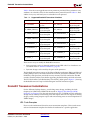
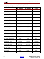
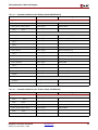
RocketIO Transceiver Instantiations
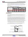
Table 1-4 lists the sixteen gigabit transceiver primitives provided. These primitives carry
attributes set to default values for the communications protocols listed in Table 1-2. Data
widths of one, two, and four bytes are selectable for each protocol.
Table 1-4:
Supported RocketIO Transceiver Primitives
Primitives
Description
Primitive
Description
GT_CUSTOM
Fully customizable
by user
GT_XAUI_2
10-Gb Ethernet,
2-byte data path
GT_FIBRE_CHAN_1
Fibre Channel,
1-byte data path
GT_XAUI_4
10-Gb Ethernet,
4-byte data path
GT_FIBRE_CHAN_2
Fibre Channel,
2-byte data path
GT_INFINIBAND_1
Infiniband, 1-byte
data path
GT_FIBRE_CHAN_4
Fibre Channel,
4-byte data path
GT_INFINIBAND_2
Infiniband, 2-byte
data path
GT_ETHERNET_1
Gigabit Ethernet,
1-byte data path
GT_INFINIBAND_4
Infiniband, 4-byte
data path
GT_ETHERNET_2
Gigabit Ethernet,
2-byte data path
GT_AURORA_1
Xilinx protocol,
1-byte data path
GT_ETHERNET_4
Gigabit Ethernet,
4-byte data path
GT_AURORA_2
Xilinx protocol,
2-byte data path
GT_XAUI_1
10-Gb Ethernet,
1-byte data path
GT_AURORA_4
Xilinx protocol,
4-byte data path
There are two ways to modify the RocketIO transceiver:
•
Static properties can be set through attributes in the HDL code. Use of attributes are
covered in detail in “Primitive Attributes,” page 26.
•
Dynamic changes can be made by the ports of the primitives
The RocketIO transceiver consists of the Physical Media Attachment (PMA) and Physical
Coding Sublayer (PCS). The PMA contains the serializer/deserializer (SERDES), TX and
RX buffers, clock generator, and clock recovery circuitry. The PCS contains the 8B/10B
encoder/decoder and the elastic buffer supporting channel bonding and clock correction.
The PCS also handles Cyclic Redundancy Check (CRC). Refer again to Figure 1-1, showing
the RocketIO transceiver top-level block diagram and FPGA interface signals.
RocketIO Transceiver Instantiations
For the different clocking schemes, several things must change, including the clock
frequency for USRCLK and USRCLK2 discussed in “Digital Clock Manager (DCM)
Examples” in Chapter 2. The data and control ports for GT_CUSTOM must also reflect this
change in data width by concatenating zeros onto inputs and wires for outputs for Verilog
designs, and by setting outputs to open and concatenating zeros on unused input bits for
VHDL designs.
HDL Code Examples
Please use the Architecture Wizard to create instantiation templates. This wizard creates
code and instantiation templates that define the attributes for a specific application.
RocketIO™ Transceiver User Guide
UG024 (v2.2) November 7, 2003
www.xilinx.com
1-800-255-7778
21
R
Chapter 1: RocketIO Transceiver Overview
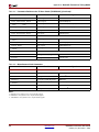
List of Available Ports
The RocketIO transceiver primitives contain 50 ports, with the exception of the 46-port
GT_ETHERNET and GT_FIBRE_CHAN primitives. The differential serial data ports
(RXN, RXP, TXN, and TXP) are connected directly to external pads; the remaining 46 ports
are all accessible from the FPGA logic (42 ports for GT_ETHERNET and
GT_FIBRE_CHAN).
Table 1-5 contains the port descriptions of all primitives.
Table 1-5: GT_CUSTOM (1), GT_AURORA, GT_FIBRE_CHAN (2), GT_ETHERNET (2),
GT_INFINIBAND, and GT_XAUI Primitive Ports
I/O
Port
Size
BREFCLK
I
1
This high-quality reference clock uses dedicated routing to improve
jitter for serial speeds of 2.5 Gbps or greater. See Table 2-2, page 38 for
usage cases.
BREFCLK2
I
1
Alternative to BREFCLK. Can be selected by REFCLKSEL.
CHBONDDONE (2)
O
1
Indicates a receiver has successfully completed channel bonding when
asserted High.
CHBONDI (2)
I
4
The channel bonding control that is used only by "slaves" which is
driven by a transceiver's CHBONDO port.
CHBONDO (2)
O
4
Channel bonding control that passes channel bonding and clock
correction control to other transceivers.
CONFIGENABLE
I
1
Reconfiguration enable input (unused)
CONFIGIN
I
1
Data input for reconfiguring transceiver (unused)
CONFIGOUT
O
1
Data output for configuration readback (unused)
ENCHANSYNC (2)
I
1
Comes from the core to the transceiver and enables the transceiver to
perform channel bonding
ENMCOMMAALIGN
I
1
Selects realignment of incoming serial bitstream on minus-comma.
High realigns serial bitstream byte boundary when minus-comma is
detected.
ENPCOMMAALIGN
I
1
Selects realignment of incoming serial bitstream on plus-comma. High
realigns serial bitstream byte boundary when plus-comma is detected.
LOOPBACK
I
2
Selects the two loopback test modes. Bit 1 is for serial loopback and bit 0
is for internal parallel loopback.
POWERDOWN
I
1
Shuts down both the receiver and transmitter sides of the transceiver
when asserted High. This decreases the power consumption while the
transceiver is shut down. This input is asynchronous.
REFCLK
I
1
High-quality reference clock driving transmission (reading TX FIFO,
and multiplied for parallel/serial conversion) and clock recovery.
REFCLK frequency is accurate to ±100 ppm. This clock originates off
the device, is routed through fabric interconnect, and is selected by
REFCLKSEL.
REFCLK2
I
1
An alternative to REFCLK. Can be selected by REFCLKSEL.
Port
22
Definition
www.xilinx.com
1-800-255-7778
RocketIO™ Transceiver User Guide
UG024 (v2.2) November 7, 2003
R
List of Available Ports
Table 1-5: GT_CUSTOM (1), GT_AURORA, GT_FIBRE_CHAN (2), GT_ETHERNET (2),
GT_INFINIBAND, and GT_XAUI Primitive Ports (Continued)
Port
REFCLKSEL
I/O
Port
Size
I
1
Definition
Selects the reference clock to use:
Low = selects REFCLK if REF_CLK_V_SEL = 0
selects BREFCLK if REF_CLK_V_SEL = 1
High = selects REFCLK2 if REF_CLK_V_SEL = 0
selects BREFCLK2 if REF_CLK_V_SEL = 1
See “REF_CLK_V_SEL,” page 29.
RXBUFSTATUS
O
2
Receiver elastic buffer status. Bit 1 indicates if an overflow/underflow
error has occurred when asserted High. Bit 0 indicates that the buffer is
at least half-full when asserted High.
RXCHARISCOMMA (3)
O
1, 2, 4
Similar to RXCHARISK except that the data is a comma.
RXCHARISK (3)
O
1, 2, 4
If 8B/10B decoding is enabled, it indicates that the received data is a
K-character when asserted High. Included in Byte-mapping. If 8B/10B
decoding is bypassed, it remains as the first bit received (Bit "a") of the
10-bit encoded data (see Figure 2-14, page 63).
RXCHECKINGCRC
O
1
CRC status for the receiver. Asserts High to indicate that the receiver
has recognized the end of a data packet. Only meaningful if
RX_CRC_USE = TRUE.
RXCLKCORCNT
O
3
Status that denotes occurrence of clock correction or channel bonding.
This status is synchronized on the incoming RXDATA. See
“RXCLKCORCNT,” page 74.
RXCOMMADET
O
1
Signals that a comma has been detected in the data stream.
To assure signal is reliably brought out to the fabric for different data
paths, this signal may remain High for more than one
USRCLK/USRCLK2 cycle.
RXCRCERR
O
1
RXDATA (3)
O
8, 16, 32
RXDISPERR (3)
O
1, 2, 4
RXLOSSOFSYNC
O
2
Indicates if the CRC code is incorrect when asserted High. Only
meaningful if RX_CRC_USE = TRUE.
Up to four bytes of decoded (8B/10B encoding) or encoded (8B/10B
bypassed) receive data.
If 8B/10B encoding is enabled it indicates whether a disparity error has
occurred on the serial line. Included in Byte-mapping scheme.
Status related to byte-stream synchronization
(RX_LOSS_OF_SYNC_FSM)
If RX_LOSS_OF_SYNC_FSM = TRUE, RXLOSSOFSYNC indicates the
state of the FSM:
Bit 1 = Loss of sync (High)
Bit 0 = Resync state (High)
If RX_LOSS_OF_SYNC_FSM = FALSE, RXLOSSOFSYNC indicates:
Bit 1 = Received data invalid (High)
Bit 0 = Channel bonding sequence recognized (High)
RocketIO™ Transceiver User Guide
UG024 (v2.2) November 7, 2003
www.xilinx.com
1-800-255-7778
23
R
Chapter 1: RocketIO Transceiver Overview
Table 1-5: GT_CUSTOM (1), GT_AURORA, GT_FIBRE_CHAN (2), GT_ETHERNET (2),
GT_INFINIBAND, and GT_XAUI Primitive Ports (Continued)
I/O
Port
Size
RXN (4)
I
1
RXNOTINTABLE (3)
O
1, 2, 4
RXP (4)
I
1
Serial differential port (FPGA external)
RXPOLARITY
I
1
Similar to TXPOLARITY, but for RXN and RXP. When de-asserted,
assumes regular polarity. When asserted, reverses polarity.
RXREALIGN
O
1
Signal from the PMA denoting that the byte alignment with the serial
data stream changed due to a comma detection. Asserted High when
alignment occurs.
RXRECCLK
O
1
Clock recovered from the data stream by dividing its speed by 20.
RXRESET
I
1
Synchronous RX system reset that "recenters" the receive elastic buffer.
It also resets 8B/10B decoder, comma detect, channel bonding, clock
correction logic, and other internal receive registers. It does not reset the
receiver PLL.
RXRUNDISP (3)
O
1, 2, 4
Signals the running disparity (0 = negative, 1 = positive) in the received
serial data. If 8B/10B encoding is bypassed, it remains as the second bit
received (Bit "b") of the 10-bit encoded data (see Figure 2-14, page 63).
RXUSRCLK
I
1
Clock from a DCM or a BUFG that is used for reading the RX elastic
buffer. It also clocks CHBONDI and CHBONDO in and out of the
transceiver. Typically, the same as TXUSRCLK.
RXUSRCLK2
I
1
Clock output from a DCM that clocks the receiver data and status
between the transceiver and the FPGA core. Typically the same as
TXUSRCLK2. The relationship between RXUSRCLK and RXUSRCLK2
depends on the width of RXDATA.
TXBUFERR
O
1
Provides status of the transmission FIFO. If asserted High, an
overflow/underflow has occurred. When this bit becomes set, it can
only be reset by asserting TXRESET.
TXBYPASS8B10B (3)
I
1, 2, 4
This control signal determines whether the 8B/10B encoding is enabled
or bypassed. If the signal is asserted High, the encoding is bypassed.
This creates a 10-bit interface to the FPGA core. See the 8B/10B section
for more details.
TXCHARDISPMODE (3)
I
1, 2, 4
If 8B/10B encoding is enabled, this bus determines what mode of
disparity is to be sent. When 8B/10B is bypassed, this becomes the first
bit transmitted (Bit "a") of the 10-bit encoded TXDATA bus section (see
Figure 2-13, page 63) for each byte specified by the byte-mapping.
TXCHARDISPVAL (3)
I
1, 2, 4
If 8B/10B encoding is enabled, this bus determines what type of
disparity is to be sent. When 8B/10B is bypassed, this becomes the
second bit transmitted (Bit "b") of the 10-bit encoded TXDATA bus
section (see Figure 2-13, page 63) for each byte specified by the bytemapping section.
Port
24
Definition
Serial differential port (FPGA external)
Status of encoded data when the data is not a valid character when
asserted High. Applies to the byte-mapping scheme.
www.xilinx.com
1-800-255-7778
RocketIO™ Transceiver User Guide
UG024 (v2.2) November 7, 2003
R
List of Available Ports
Table 1-5: GT_CUSTOM (1), GT_AURORA, GT_FIBRE_CHAN (2), GT_ETHERNET (2),
GT_INFINIBAND, and GT_XAUI Primitive Ports (Continued)
I/O
Port
Size
TXCHARISK (3)
I
1, 2, 4
TXDATA (3)
I
8, 16, 32
TXFORCECRCERR
I
1
Specifies whether to insert error in computed CRC.
When TXFORCECRCERR = TRUE, the transmitter corrupts the
correctly computed CRC value by XORing with the bits specified in
attribute TX_CRC_FORCE_VALUE. This input can be used to test
detection of CRC errors at the receiver.
TXINHIBIT
I
1
If a logic High, the TX differential pairs are forced to be a constant 1/0.
TXN = 1, TXP = 0
TXKERR (3)
O
1, 2, 4
If 8B/10B encoding is enabled, this signal indicates (High) when the
K-character to be transmitted is not a valid K-character. Bits correspond
to the byte-mapping scheme.
TXN (4)
O
1
Transmit differential port (FPGA external)
TXP (4)
O
1
Transmit differential port (FPGA external)
TXPOLARITY
I
1
Specifies whether or not to invert the final transmitter output. Able to
reverse the polarity on the TXN and TXP lines. Deasserted sets regular
polarity. Asserted reverses polarity.
TXRESET
I
1
Synchronous TX system reset that “recenters” the transmit elastic
buffer. It also resets 8B/10B encoder and other internal transmission
registers. It does not reset the transmission PLL.
TXRUNDISP (3)
O
1, 2, 4
Signals the running disparity after this byte is encoded. Low indicates
negative disparity, High indicates positive disparity.
TXUSRCLK
I
1
Clock output from a DCM or a BUFG that is clocked with a reference
clock. This clock is used for writing the TX buffer and is frequencylocked to the reference clock.
TXUSRCLK2
I
1
Clock output from a DCM that clocks transmission data and status and
reconfiguration data between the transceiver an the FPGA core. The
ratio between TXUSRCLK and TXUSRCLK2 depends on the width of
TXDATA.
Port
Definition
If 8B/10B encoding is enabled, this control bus determines if the
transmitted data is a K-character or a Data character. A logic High
indicates a K-character.
Transmit data that can be 1, 2, or 4 bytes wide, depending on the
primitive used. TXDATA [7:0] is always the last byte transmitted. The
position of the first byte depends on selected TX data path width.
Notes:
1. The GT_CUSTOM ports are always the maximum port size.
2. GT_FIBRE_CHAN and GT_ETHERNET ports do not have the three CHBOND** or ENCHANSYNC ports.
3. The port size changes with relation to the primitive selected, and also correlates to the byte mapping.
4. External ports only accessible from package pins.
RocketIO™ Transceiver User Guide
UG024 (v2.2) November 7, 2003
www.xilinx.com
1-800-255-7778
25
R
Chapter 1: RocketIO Transceiver Overview
Primitive Attributes
The primitives also contain attributes set by default to specific values controlling each
specific primitive’s protocol parameters. Included are channel-bonding settings (for
primitives supporting channel bonding), clock correction sequences, and CRC. Table 1-6
shows a brief description of each attribute. Table 1-7 and Table 1-8 have the default values
of each primitive.
Table 1-6:
RocketIO Transceiver Attributes
Attribute
ALIGN_COMMA_MSB
Description
TRUE/FALSE controls the alignment of detected commas within the
transceiver’s 2-byte-wide data path.
FALSE: Align commas within a 10-bit alignment range. As a result the
comma is aligned to either RXDATA[15:8} byte or RXDATA [7:0] byte in
the transceivers internal data path.
TRUE: Aligns comma with 20-bit alignment range.
As a result aligns on the RXDATA[15:8] byte.
Notes:
1. If protocols (like Gigabit Ethernet) are oriented in byte pairs with commas always in
even (first) byte formation, this can be set to TRUE. Otherwise, it should be set to
FALSE.
2. For 32-bit data path primitives, see “32-bit Alignment Design,” page 91.
3. This attribute is only modifiable in the GT_CUSTOM primitive.
CHAN_BOND_LIMIT
Integer 1-31 that defines maximum number of bytes a slave receiver can read
following a channel bonding sequence and still successfully align to that
sequence.
CHAN_BOND_MODE
STRING
OFF, MASTER, SLAVE_1_HOP, SLAVE_2_HOPS
OFF: No channel bonding involving this transceiver.
MASTER: This transceiver is master for channel bonding. Its CHBONDO
port directly drives CHBONDI ports on one or more SLAVE_1_HOP
transceivers.
SLAVE_1_HOP: This transceiver is a slave for channel bonding.
SLAVE_1_HOP’s CHBONDI is directly driven by a MASTER transceiver
CHBONDO port. SLAVE_1_HOP’s CHBONDO port can directly drive
CHBONDI ports on one or more SLAVE_2_HOPS transceivers.
SLAVE_2_HOPS: This transceiver is a slave for channel bonding.
SLAVE_2_HOPS CHBONDI is directly driven by a SLAVE_1_HOP
CHBONDO port.
26
www.xilinx.com
1-800-255-7778
RocketIO™ Transceiver User Guide
UG024 (v2.2) November 7, 2003
R
Primitive Attributes
Table 1-6:
RocketIO Transceiver Attributes (Continued)
Attribute
CHAN_BOND_OFFSET
Description
Integer 0-15 that defines offset (in bytes) from channel bonding sequence for
realignment. It specifies the first elastic buffer read address that all channelbonded transceivers have immediately after channel bonding.
CHAN_BOND_WAIT specifies the number of bytes that the master
transceiver passes to RXDATA, starting with the channel bonding sequence,
before the transceiver executes channel bonding (alignment) across all
channel-bonded transceivers.
CHAN_BOND_OFFSET specifies the first elastic buffer read address that all
channel-bonded transceivers have immediately after channel bonding
(alignment), as a positive offset from the beginning of the matched channel
bonding sequence in each transceiver.
For optimal performance of the elastic buffer, CHAN_BOND_WAIT and
CHAN_BOND_OFFSET should be set to the same value (typically 8).
CHAN_BOND_ONE_SHOT
TRUE/FALSE that controls repeated execution of channel bonding.
FALSE: Master transceiver initiates channel bonding whenever possible
(whenever channel-bonding sequence is detected in the input) as long as
input ENCHANSYNC is High and RXRESET is Low.
TRUE: Master transceiver initiates channel bonding only the first time it
is possible (channel bonding sequence is detected in input) following
negated RXRESET and asserted ENCHANSYNC. After channel-bonding
alignment is done, it does not occur again until RXRESET is asserted and
negated, or until ENCHANSYNC is negated and reasserted.
Always set Slave transceivers CHAN_BOND_ONE_SHOT to FALSE.
CHAN_BOND_SEQ_*_*
11-bit vectors that define the channel bonding sequence. The usage of these
vectors also depends on CHAN_BOND_SEQ_LEN and
CHAN_BOND_SEQ_2_USE. See “Receiving Vitesse Channel Bonding
Sequence,” page 63, for format.
CHAN_BOND_SEQ_2_USE
Controls use of second channel bonding sequence.
FALSE: Channel bonding uses only one channel bonding sequence
defined by CHAN_BOND_SEQ_1_1..4.
TRUE: Channel bonding uses two channel bonding sequences defined
by:
CHAN_BOND_SEQ_1_1..4 and
CHAN_BOND_SEQ_2_1..4
as further constrained by CHAN_BOND_SEQ_LEN.
CHAN_BOND_SEQ_LEN
Integer 1-4 defines length in bytes of channel bonding sequence. This
defines the length of the sequence the transceiver matches to detect
opportunities for channel bonding.
CHAN_BOND_WAIT
Integer 1-15 that defines the length of wait (in bytes) after seeing channel
bonding sequence before executing channel bonding.
RocketIO™ Transceiver User Guide
UG024 (v2.2) November 7, 2003
www.xilinx.com
1-800-255-7778
27
R
Table 1-6:
Chapter 1: RocketIO Transceiver Overview
RocketIO Transceiver Attributes (Continued)
Attribute
Description
CLK_COR_INSERT_IDLE_FLAG
TRUE/FALSE controls whether RXRUNDISP input status denotes running
disparity or inserted-idle flag.
FALSE: RXRUNDISP denotes running disparity when RXDATA is
decoded data.
TRUE: RXRUNDISP is raised for the first byte of each inserted (repeated)
clock correction ("Idle") sequence (when RXDATA is decoded data).
CLK_COR_KEEP_IDLE
TRUE/FALSE controls whether or not the final byte stream must retain at
least one clock correction sequence.
FALSE: Transceiver can remove all clock correction sequences to further
recenter the elastic buffer during clock correction.
TRUE: In the final RXDATA stream, the transceiver must leave at least
one clock correction sequence per continuous stream of clock correction
sequences.
CLK_COR_REPEAT_WAIT
Integer 0 - 31 controls frequency of repetition of clock correction operations.
This attribute specifies the minimum number of RXUSRCLK cycles without
clock correction that must occur between successive clock corrections. If this
attribute is zero, no limit is placed on how frequently clock correction can
occur.
CLK_COR_SEQ_*_*
11-bit vectors that define the sequence for clock correction. The attribute
used depends on the CLK_COR_SEQ_LEN and CLK_COR_SEQ_2_USE.
CLK_COR_SEQ_2_USE
TRUE/FALSE controls use of second clock correction sequence.
FALSE: Clock correction uses only one clock correction sequence defined
by CLK_COR_SEQ_1_1..4.
TRUE: Clock correction uses two clock correction sequences defined by:
CLK_COR_SEQ_1_1..4 and
CLK_COR_SEQ_2_1..4
as further constrained by CLK_COR_SEQ_LEN.
CLK_COR_SEQ_LEN
Integer that defines the length of the sequence the transceiver matches to
detect opportunities for clock correction. It also defines the size of the
correction, since the transceiver executes clock correction by repeating or
skipping entire clock correction sequences.
CLK_CORRECT_USE
TRUE/FALSE controls the use of clock correction logic.
FALSE: Permanently disable execution of clock correction (rate
matching). Clock RXUSRCLK must be frequency-locked with
RXRECCLK in this case.
TRUE: Enable clock correction (normal mode).
COMMA_10B_MASK
28
This 10-bit vector defines the mask that is ANDed with the incoming serial
bit stream before comparison against PCOMMA_10B_VALUE and
MCOMMA_10B_VALUE.
www.xilinx.com
1-800-255-7778
RocketIO™ Transceiver User Guide
UG024 (v2.2) November 7, 2003
R
Primitive Attributes
Table 1-6:
RocketIO Transceiver Attributes (Continued)
Attribute
CRC_END_OF_PKT
Description
NOTE: This attribute is only valid when CRC_FORMAT = USER_MODE.
K28_0, K28_1, K28_2, K28_3, K28_4, K28_5, K28_6, K28_7, K23_7, K27_7,
K29_7, K30_7. End-of-packet (EOP) K-character for USER_MODE CRC.
Must be one of the 12 legal K-character values.
CRC_FORMAT
ETHERNET, INFINIBAND, FIBRE_CHAN, USER_MODE CRC algorithm
selection. Modifiable only for GT_AURORA_n, GT_XAUI_n, and
GT_CUSTOM. USER_MODE allows user definition of Start of Packet (SOP)
and End of Packet (EOP) K-characters.
CRC_START_OF_PKT
NOTE: This attribute is only valid when CRC_FORMAT = USER_MODE.
K28_0, K28_1, K28_2, K28_3, K28_4, K28_5, K28_6, K28_7, K23_7, K27_7,
K29_7, K30_7. Start-of-packet (SOP) K-character for USER_MODE CRC.
Must be one of the twelve legal K-character values.
DEC_MCOMMA_DETECT
TRUE/FALSE controls the raising of per-byte flag RXCHARISCOMMA on
minus-comma.
DEC_PCOMMA_DETECT
TRUE/FALSE controls the raising of per-byte flag RXCHARISCOMMA on
plus-comma.
DEC_VALID_COMMA_ONLY
TRUE/FALSE controls the raising of RXCHARISCOMMA on an invalid
comma.
FALSE: Raise RXCHARISCOMMA on:
0011111xxx
(if DEC_PCOMMA_DETECT is TRUE)
and/or on:
1100000xxx
(if DEC_MCOMMA_DETECT is TRUE)
regardless of the settings of the xxx bits.
TRUE: Raise RXCHARISCOMMA only on valid characters that are in the
8B/10B translation.
MCOMMA_10B_VALUE
This 10-bit vector defines minus-comma for the purpose of raising
RXCOMMADET and realigning the serial bit stream byte boundary. This
definition does not affect 8B/10B encoding or decoding. Also see
COMMA_10B_MASK.
MCOMMA_DETECT
TRUE/FALSE indicates whether to raise or not raise RXCOMMADET when
minus-comma is detected.
PCOMMA_10B_VALUE
This 10-bit vector defines plus-comma for the purpose of raising
RXCOMMADET and realigning the serial bit stream byte boundary. This
definition does not affect 8B/10B encoding or decoding. Also see
COMMA_10B_MASK.
PCOMMA_DETECT
TRUE/FALSE indicates whether to raise or not raise RXCOMMADET when
plus-comma is detected.
REF_CLK_V_SEL
1/0:
1: Selects BREFCLK/BREFCLK2 for 2.5 Gbps or greater serial speeds.
0: Selects REFCLK/REFCLK2 for serial speeds under 2.5 Gbps.
RocketIO™ Transceiver User Guide
UG024 (v2.2) November 7, 2003
www.xilinx.com
1-800-255-7778
29
R
Table 1-6:
Chapter 1: RocketIO Transceiver Overview
RocketIO Transceiver Attributes (Continued)
Attribute
Description
RX_BUFFER_USE
Always set to TRUE.
RX_CRC_USE,
TX_CRC_USE
TRUE/FALSE determines if CRC is used or not.
RX_DATA_WIDTH,
TX_DATA_WIDTH
Integer (1, 2, or 4). Relates to the data width of the FPGA fabric interface.
RX_DECODE_USE
This determines if the 8B/10B decoding is bypassed. FALSE denotes that it
is bypassed.
RX_LOS_INVALID_INCR
Power of two in a range of 1 to 128 that denotes the number of valid
characters required to "cancel out" appearance of one invalid character for
loss of sync determination.
RX_LOS_THRESHOLD
Power of two in a range of 4 to 512. When divided by
RX_LOS_INVALID_INCR, denotes the number of invalid characters
required to cause FSM transition to "sync lost" state.
RX_LOSS_OF_SYNC_FSM
TRUE/FALSE denotes the nature of RXLOSSOFSYNC output.
TRUE: RXLOSSOFSYNC outputs the state of the FSM bits.
See “RXLOSSOFSYNC,” page 23, for details.
SERDES_10B
Denotes whether the reference clock is 1/10 or 1/20 the serial bit rate.
TRUE: 1/10
FALSE: 1/20
FALSE supports a serial bitstream range of 1.0 Gbps to 3.125 Gbps.
TRUE supports a range of 600 Mbps to 1.0 Gbps.
See “Half-Rate Clocking Scheme,” page 52.
TERMINATION_IMP
Integer (50 or 75). Termination impedance of either 50Ω or 75Ω. Refers to
both the RX and TX.
TX_BUFFER_USE
Always set to TRUE.
TX_CRC_FORCE_VALUE
8-bit vector. Value to corrupt TX CRC computation when input
TXFORCECRCERR is High. This value is XORed with the correctly
computed CRC value, corrupting the CRC if TX_CRC_FORCE_VALUE is
nonzero. This can be used to test CRC error detection in the receiver
downstream.
TX_DIFF_CTRL
An integer value (400, 500, 600, 700, or 800) representing 400 mV, 500 mV,
600 mV, 700 mV, or 800 mV of voltage difference between the differential
lines. Twice this value is the peak-peak voltage.
TX_PREEMPHASIS
An integer value (0-3) that sets the output driver pre-emphasis to improve
output waveform shaping for various load conditions. Larger value denotes
stronger pre-emphasis. See pre-emphasis values in Table 3-2, page 100.
30
www.xilinx.com
1-800-255-7778
RocketIO™ Transceiver User Guide
UG024 (v2.2) November 7, 2003
R
Modifiable Primitives
Modifiable Primitives
As shown in Table 1-7 and Table 1-8, only certain attributes are modifiable for any
primitive. These attributes help to define the protocol used by the primitive. Only the
GT_CUSTOM primitive allows the user to modify all of the attributes to a protocol not
supported by another transceiver primitive. This allows for complete flexibility. The other
primitives allow modification of the analog attributes of the serial data lines and several
channel-bonding values.
Table 1-7:
Default Attribute Values: GT_AURORA, GT_CUSTOM, GT_ETHERNET
Default
GT_AURORA
Default
GT_CUSTOM (1)
Default
GT_ETHERNET
ALIGN_COMMA_MSB
FALSE
FALSE
FALSE
CHAN_BOND_LIMIT
16
16
1
CHAN_BOND_MODE
OFF (2)
OFF
OFF
CHAN_BOND_OFFSET
8
8
0
FALSE (2)
FALSE
TRUE
CHAN_BOND_SEQ_1_1
00101111100
00000000000
00000000000
CHAN_BOND_SEQ_1_2
00000000000
00000000000
00000000000
CHAN_BOND_SEQ_1_3
00000000000
00000000000
00000000000
CHAN_BOND_SEQ_1_4
00000000000
00000000000
00000000000
CHAN_BOND_SEQ_2_1
00000000000
00000000000
00000000000
CHAN_BOND_SEQ_2_2
00000000000
00000000000
00000000000
CHAN_BOND_SEQ_2_3
00000000000
00000000000
00000000000
CHAN_BOND_SEQ_2_4
00000000000
00000000000
00000000000
FALSE
FALSE
FALSE
CHAN_BOND_SEQ_LEN
1
1
1
CHAN_BOND_WAIT
8
8
7
CLK_COR_INSERT_IDLE_FLAG
FALSE (2)
FALSE
FALSE (2)
CLK_COR_KEEP_IDLE
FALSE (2)
FALSE
FALSE (2)
1 (2)
1
1 (2)
CLK_COR_SEQ_1_1
00111110111
00000000000
00110111100
CLK_COR_SEQ_1_2
00111110111
00000000000
00001010000
CLK_COR_SEQ_1_3
00111110111 (5)
00000000000
00000000000
CLK_COR_SEQ_1_4
00111110111 (5)
00000000000
00000000000
CLK_COR_SEQ_2_1
00000000000
00000000000
00000000000
Attribute
CHAN_BOND_ONE_SHOT
CHAN_BOND_SEQ_2_USE
CLK_COR_REPEAT_WAIT
RocketIO™ Transceiver User Guide
UG024 (v2.2) November 7, 2003
www.xilinx.com
1-800-255-7778
31
R
Table 1-7:
Chapter 1: RocketIO Transceiver Overview
Default Attribute Values: GT_AURORA, GT_CUSTOM, GT_ETHERNET (Continued)
Default
GT_AURORA
Default
GT_CUSTOM (1)
Default
GT_ETHERNET
CLK_COR_SEQ_2_2
00000000000
00000000000
00000000000
CLK_COR_SEQ_2_3
00000000000
00000000000
00000000000
CLK_COR_SEQ_2_4
00000000000
00000000000
00000000000
FALSE
FALSE
FALSE
CLK_COR_SEQ_LEN
4 (4)
1
2
CLK_CORRECT_USE
TRUE
TRUE
TRUE
COMMA_10B_MASK
1111111111
1111111000
1111111000
K29_7
K29_7
Note (6)
USER_MODE
USER_MODE
ETHERNET
CRC_START_OF_PKT
K27_7
K27_7
Note (6)
DEC_MCOMMA_DETECT
TRUE
TRUE
TRUE
DEC_PCOMMA_DETECT
TRUE
TRUE
TRUE
DEC_VALID_COMMA_ONLY
TRUE
TRUE
TRUE
1100000101
1100000000
1100000000
TRUE
TRUE
TRUE
0011111010
0011111000
0011111000
TRUE
TRUE
TRUE
REF_CLK_V_SEL
0
0
0
RX_BUFFER_USE
TRUE
TRUE
TRUE
FALSE (2)
FALSE
FALSE (2)
RX_DATA_WIDTH
N (3)
2
N (3)
RX_DECODE_USE
TRUE
TRUE
TRUE
RX_LOS_INVALID_INCR
1 (2)
1
1 (2)
RX_LOS_THRESHOLD
4 (2)
4
4 (2)
RX_LOSS_OF_SYNC_FSM
TRUE (2)
TRUE
TRUE (2)
SERDES_10B
FALSE (2)
FALSE
FALSE (2)
50 (2)
50
50 (2)
TRUE
TRUE
TRUE
11010110 (2)
11010110
11010110 (2)
FALSE (2)
FALSE
FALSE (2)
Attribute
CLK_COR_SEQ_2_USE
CRC_END_OF_PKT
CRC_FORMAT
MCOMMA_10B_VALUE
MCOMMA_DETECT
PCOMMA_10B_VALUE
PCOMMA_DETECT
RX_CRC_USE
TERMINATION_IMP
TX_BUFFER_USE
TX_CRC_FORCE_VALUE
TX_CRC_USE
32
www.xilinx.com
1-800-255-7778
RocketIO™ Transceiver User Guide
UG024 (v2.2) November 7, 2003
R
Modifiable Primitives
Table 1-7:
Default Attribute Values: GT_AURORA, GT_CUSTOM, GT_ETHERNET (Continued)
Attribute
TX_DATA_WIDTH
TX_DIFF_CTRL
TX_PREEMPHASIS
Default
GT_AURORA
Default
GT_CUSTOM (1)
Default
GT_ETHERNET
N (3)
2
N (3)
500 (2)
500
500 (2)
0 (2)
0
0 (2)
Notes:
1. All GT_CUSTOM attributes are modifiable.
2. Modifiable attribute for specific primitives.
3. Depends on primitive used: either 1, 2, or 4.
4. Attribute value only when RX_DATA_WIDTH is 4. When RX_DATA_WIDTH is 1 or 2, attribute value is 2.
5. Attribute value only when RX_DATA_WIDTH is 4. When RX_DATA_WIDTH is 1 or 2, attribute value is 0.
6. CRC_EOP and CRC_SOP are not applicable for this primitive.
Table 1-8: Default Attribute Values: GT_FIBRE_CHAN, GT_INFINIBAND,
and GT_XAUI
Default
GT_FIBRE_CHAN
Default
GT_INFINIBAND
Default
GT_XAUI
ALIGN_COMMA_MSB
FALSE
FALSE
FALSE
CHAN_BOND_LIMIT
1
16
16
CHAN_BOND_MODE
OFF
OFF (1)
OFF (1)
CHAN_BOND_OFFSET
0
8
8
TRUE
FALSE (1)
FALSE (1)
CHAN_BOND_SEQ_1_1
00000000000
00110111100
00101111100
CHAN_BOND_SEQ_1_2
00000000000
Lane ID (Modify with
Lane ID)
00000000000
CHAN_BOND_SEQ_1_3
00000000000
00001001010
00000000000
CHAN_BOND_SEQ_1_4
00000000000
00001001010
00000000000
CHAN_BOND_SEQ_2_1
00000000000
00110111100
00000000000
CHAN_BOND_SEQ_2_2
00000000000
Lane ID (Modify with
Lane ID)
00000000000
CHAN_BOND_SEQ_2_3
00000000000
00001000101
00000000000
CHAN_BOND_SEQ_2_4
00000000000
00001000101
00000000000
FALSE
TRUE
FALSE
CHAN_BOND_SEQ_LEN
1
4
1
CHAN_BOND_WAIT
7
8
8
FALSE (1)
FALSE (1)
FALSE (1)
Attribute
CHAN_BOND_ONE_SHOT
CHAN_BOND_SEQ_2_USE
CLK_COR_INSERT_IDLE_FLAG
RocketIO™ Transceiver User Guide
UG024 (v2.2) November 7, 2003
www.xilinx.com
1-800-255-7778
33
R
Chapter 1: RocketIO Transceiver Overview
Table 1-8: Default Attribute Values: GT_FIBRE_CHAN, GT_INFINIBAND,
and GT_XAUI (Continued)
Default
GT_FIBRE_CHAN
Default
GT_INFINIBAND
Default
GT_XAUI
FALSE (1)
FALSE (1)
FALSE (1)
2 (1)
1 (1)
1 (1)
CLK_COR_SEQ_1_1
00110111100
00100011100
00100011100
CLK_COR_SEQ_1_2
00010010101
00000000000
00000000000
CLK_COR_SEQ_1_3
00010110101
00000000000
00000000000
CLK_COR_SEQ_1_4
00010110101
00000000000
00000000000
CLK_COR_SEQ_2_1
00000000000
00000000000
00000000000
CLK_COR_SEQ_2_2
00000000000
00000000000
00000000000
CLK_COR_SEQ_2_3
00000000000
00000000000
00000000000
CLK_COR_SEQ_2_4
00000000000
00000000000
00000000000
FALSE
FALSE
FALSE
CLK_COR_SEQ_LEN
4
1
1
CLK_CORRECT_USE
TRUE
TRUE
TRUE
COMMA_10B_MASK
1111111000
1111111000
1111111000
Note (3)
Note (3)
K29_7 (1)
FIBRE_CHAN
INFINIBAND
USER_MODE (1)
Note (3)
Note (3)
K27_7 (1)
DEC_MCOMMA_DETECT
TRUE
TRUE
TRUE
DEC_PCOMMA_DETECT
TRUE
TRUE
TRUE
DEC_VALID_COMMA_ONLY
TRUE
TRUE
TRUE
Lane ID(INFINBAND ONLY)
NA
00000000000 (1)
NA
1100000000
1100000000
1100000000
TRUE
TRUE
TRUE
0011111000
0011111000
0011111000
TRUE
TRUE
TRUE
REF_CLK_V_SEL
0
0
0
RX_BUFFER_USE
TRUE
TRUE
TRUE
FALSE (1)
FALSE (1)
FALSE (1)
N (2)
N (2)
N (2)
Attribute
CLK_COR_KEEP_IDLE
CLK_COR_REPEAT_WAIT
CLK_COR_SEQ_2_USE
CRC_END_OF_PKT
CRC_FORMAT
CRC_START_OF_PKT
MCOMMA_10B_VALUE
MCOMMA_DETECT
PCOMMA_10B_VALUE
PCOMMA_DETECT
RX_CRC_USE
RX_DATA_WIDTH
34
www.xilinx.com
1-800-255-7778
RocketIO™ Transceiver User Guide
UG024 (v2.2) November 7, 2003
R
Byte Mapping
Table 1-8: Default Attribute Values: GT_FIBRE_CHAN, GT_INFINIBAND,
and GT_XAUI (Continued)
Default
GT_FIBRE_CHAN
Default
GT_INFINIBAND
Default
GT_XAUI
TRUE
TRUE
TRUE
RX_LOS_INVALID_INCR
1 (1)
1 (1)
1 (1)
RX_LOS_THRESHOLD
4 (1)
4 (1)
4 (1)
RX_LOSS_OF_SYNC_FSM
TRUE (1)
TRUE (1)
TRUE (1)
SERDES_10B
FALSE (1)
FALSE (1)
FALSE (1)
50 (1)
50 (1)
50 (1)
TRUE
TRUE
TRUE
11010110 (1)
11010110 (1)
11010110 (1)
FALSE (1)
FALSE (1)
FALSE (1)
N (2)
N (2)
N (2)
500 (1)
500 (1)
500 (1)
0 (1)
0 (1)
0 (1)
Attribute
RX_DECODE_USE
TERMINATION_IMP
TX_BUFFER_USE
TX_CRC_FORCE_VALUE
TX_CRC_USE
TX_DATA_WIDTH
TX_DIFF_CTRL
TX_PREEMPHASIS
Notes:
1. Modifiable attribute for specific primitives.
2. Depends on primitive used: either 1, 2, or 4.
3. CRC_EOP and CRC_SOP are not applicable for this primitive.
Byte Mapping
Most of the 4-bit wide status and control buses correlate to a specific byte of TXDATA or
RXDATA. This scheme is shown in Table 1-9. This creates a way to tie all the signals
together regardless of the data path width needed for the GT_CUSTOM. All other
primitives with specific data width paths and all byte-mapped ports are affected by this
situation. For example, a 1-byte wide data path has only 1-bit control and status bits
(TXKERR[0]) correlating to the data bits TXDATA[7:0]. Footnote 3 in Table 1-5 shows the
ports that use byte mapping.
Table 1-9:
Control/Status Bus Association to Data Bus Byte Paths
Control/Status Bit
Data Bits
[0]
[7:0]
[1]
[15:8]
[2]
[23:16]
[3]
[31:24]
RocketIO™ Transceiver User Guide
UG024 (v2.2) November 7, 2003
www.xilinx.com
1-800-255-7778
35
R
36
Chapter 1: RocketIO Transceiver Overview
www.xilinx.com
1-800-255-7778
RocketIO™ Transceiver User Guide
UG024 (v2.2) November 7, 2003
R
Chapter 2
Digital Design Considerations
Clocking
Clock Signals
There are eight clock inputs into each RocketIO transceiver instantiation (Table 2-1).
REFCLK and BREFCLK are reference clocks generated from an external source and
presented to the FPGA as differential inputs. The reference clocks connect to the REFCLK
or BREFCLK ports of the RocketIO multi-gigabit transceiver (MGT). While only one of
these reference clocks is needed to drive the MGT, BREFCLK or BREFCLK2 must be used
for serial speeds of 2.5 Gbps or greater. (See “BREFCLK,” page 38.)
The PLL architecture for the transceiver uses the reference clock as the interpolation source
to clock the serial data. Removing the reference clock will stop the RX and TX PLLs from
working. Therefore, a reference clock must be provided at all times.
The reference clock also clocks a Digital Clock Manager (DCM) or a BUFG to generate all of
the other clocks for the MGT. Never run a reference clock through a DCM, since unwanted
jitter will be introduced. Any additional jitter on the reference clock will be transferred to
the transceiver’s RX and TX serial I/O.
It is recommended that all reference clock sources into the FPGA be LVDS or LVPECL
IBUFGDS. The DCI or DT attributes of LVDS are optional. Refer to the Virtex-II Pro Platform
FPGA User Guide (Chapter 3, “Design Considerations”) for a complete listing and
discussion of IBUFGDS and other available I/O primitives. Also see section “Reference
Clock” in Chapter 3 of this Guide.
Typically, TXUSRCLK = RXUSRCLK and TXUSRCLK2 = RXUSRCLK2. The transceiver
uses one or two clocks generated by the DCM. As an example, USRCLK and USRCLK2
clocks run at the same speed if the 2-byte data path is used. The USRCLK must always be
frequency-locked to the reference clock of the RocketIO transceiver when SERDES_10B =
FALSE (full-rate operation).
Note: The reference clock must be at least 50 MHz (for full-rate operation only; 60 MHz for halfrate operation) with a duty cycle between 45% and 55%, and should have a frequency stability of
±100 ppm or better, with jitter as low as possible. Module 3 of the Virtex-II Pro data sheet gives
further details.
Table 2-1:
Clock Ports
Clock
I/Os
Description
BREFCLK
Input
Reference clock used to read the TX FIFO and multiplied by
20 for parallel-to-serial conversion (20X)
BREFCLK2
Input
Alternative to BREFCLK
RocketIO™ Transceiver User Guide
UG024 (v2.2) November 7, 2003
www.xilinx.com
1-800-255-7778
37
R
Chapter 2: Digital Design Considerations
Table 2-1:
Clock Ports (Continued)
Clock
I/Os
RXRECCLK
Description
Output
Recovered clock (from serial data stream) divided by 20.
Clocks data into the elastic buffer.
REFCLK
Input
Reference clock used to read the TX FIFO and multiplied by
20 for parallel-to-serial conversion (20X)
REFCLK2
Input
Alternative to REFCLK.
REFCLKSEL
Input
Selects which reference clock is used. 0 selects REFCLK;
1 selects REFCLK2.
RXUSRCLK
Input
Clock from FPGA used for reading the RX Elastic Buffer.
Clock signals CHBONDI and CHBONDO into and out of the
transceiver. This clock is typically the same as TXUSRCLK.
TXUSRCLK(1)
Input
Clock from FPGA used for writing the TX Buffer. This clock
must be frequency locked to REFCLK for proper operation.
RXUSRCLK2
Input
Clock from FPGA used to clock RX data and status between
the transceiver and FPGA fabric. The relationship between
RXUSRCLK2 and RXUSRCLK depends on the width of the
receiver data path. RXUSRCLK2 is typically the same as
TXUSRCLK2.
TXUSRCLK2(1)
Input
Clock from FPGA used to clock TX data and status between
the transceiver and FPGA fabric. The relationship between
TXUSRCLK2 and TXUSRCLK depends on the width of the
transmission data path.
Notes:
1. TXUSRCLK and TXUSRCLK2 must be driven by clock sources, even if only the receiver of the MGT is
being used.
Table 2-2:
Reference Clock Usage
Data Rate
600 Mbps –
2.499 Gbps
REFCLK
√
BREFCLK
√
Routing
2.500 Gbps –
3.125 Gbps
√
Can Route
Across Chip?
Can Route
Through BUFG?
√
√
Note (1)
Note (1)
Notes:
1. Because of dedicated routing to reduce jitter, BREFCLK cannot be routed through the fabric.
BREFCLK
At speeds of 2.5 Gbps or greater, REFCLK configuration introduces more than the
maximum allowable jitter to the RocketIO transceiver. For these higher speeds, BREFCLK
configuration is required. The BREFCLK configuration uses dedicated routing resources
that reduce jitter.
BREFCLK must enter the FPGA through dedicated clock I/O. BREFCLK can connect to the
BREFCLK inputs of the transceiver and the CLKIN input of the DCM for creation of
38
www.xilinx.com
1-800-255-7778
RocketIO™ Transceiver User Guide
UG024 (v2.2) November 7, 2003
R
Clocking
USRCLKs. If all the transceivers on a Virtex-II Pro FPGA are to be used, two BREFCLKs
must be created, one for the top of the chip and one for the bottom. These dedicated clocks
use the same clock inputs for all packages:
BREFCLK
Top
BREFCLK2
P
GCLK4S
N
GCLK5P
P
GCLK2S
N
GCLK3P
BREFCLK
Bottom
BREFCLK2
P
GCLK6P
N
GCLK7S
P
GCLK0P
N
GCLK1S
An attribute (REF_CLK_V_SEL) and a port (REFCLKSEL) determine which reference clock
is used for the MGT PMA block. Figure 2-1 shows how REFCLK and BREFCLK are
selected through use of REFCLKSEL and REF_CLK_V_SEL.
refclk
REF_CLK_V_SEL
0
1.5V
refclk2
1
0
REFCLKSEL
refclk_out
to PCS and PMA
1
brefclk
0
2.5V
brefclk2
1
ug024_35_091802
Figure 2-1: REFCLK/BREFCLK Selection Logic
Table 2-3 shows the BREFCLK pin numbers for all packages. Note that these pads must be
used for BREFCLK operations.
Table 2-3:
BREFCLK Pin Numbers
Top
Package
Bottom
BREFCLK
Pin Number
BREFCLK2
Pin Number
BREFCLK
Pin Number
BREFCLK2
Pin Number
FG256
A8/B8
B9/A9
R8/T8
T9/R9
FG456
C11/D11
D12/C12
W11/Y11
Y12/W12
FF672
B14/C14
C13/B13
AD14/AE14
AE13/AD13
FF896
F16/G16
G15/F15
AH16/AJ16
AJ15/AH15
FF1152
H18/J18
J17/H17
AK18/AL18
AL17/AK17
FF1148
N/A
N/A
N/A
N/A
FF1517
E20/D20
J20/K20
AR20/AT20
AL20/AK20
FF1704
G22/F22
F21/G21
AU22/AT22
AT21/AU21
FF1696
N/A
N/A
N/A
N/A
RocketIO™ Transceiver User Guide
UG024 (v2.2) November 7, 2003
www.xilinx.com
1-800-255-7778
39
R
Chapter 2: Digital Design Considerations
Clock Ratio
USRCLK2 clocks the data buffers. The ability to send/receive parallel data to/from the
transceiver at three different widths requires the user to change the frequency of
USRCLK2. This creates a frequency ratio between USRCLK and USRCLK2. The falling
edges of the clocks must align. Table 2-4 shows the ratios for each of the three data widths.
Table 2-4:
Data Width Clock Ratios
Data Width
Frequency Ratio of USRCLK\USRCLK2
1 byte
1:2 (1)
2 byte
1:1
4 byte
2:1 (1)
Notes:
1. Each edge of the slower clock must align with the falling edge of the faster clock.
Digital Clock Manager (DCM) Examples
With at least three different clocking schemes possible on the transceiver, a DCM is the best
way to create these schemes.
Table 2-5 shows typical DCM connections for several transceiver clocks. REFCLK is the
input reference clock for the DCM. The other clocks are generated by the DCM. The DCM
establishes a desired phase relationship between TXUSRCLK, TXUSRCLK2, etc. in the
FPGA core and REFCLK at the pad.
NOTE: The reference clock may be any of the four MGT clocks, including the BREFCLKs.
Table 2-5:
DCM Outputs for Different DATA_WIDTHs
SERDES_10B
TX_DATA_WIDTH
RX_DATA_WIDTH
REFCLK
TXUSRCLK
RXUSRCLK
TXUSRCLK2
RXUSRCLK2
FALSE
1
CLKIN
CLK0
CLK2X180
FALSE
2
CLKIN
CLK0
CLK0
FALSE
4
CLKIN
CLK180 (1)
CLKDV (divide by 2)
TRUE
1
CLKIN
CLKDV (divide by 2)
CLK180 (1)
TRUE
2
CLKIN
CLKDV (divide by 2)
CLKDV (divide by 2)
TRUE
4
CLKIN
CLKFX180 (divide by 2)
CLKDV (divide by 4)
Notes:
1. Since CLK0 is needed for feedback, it can be used instead of CLK180 to clock USRCLK or USRCLK2 of the transceiver with the use
of the transceiver’s local inverter, saving a global buffer (BUFG).
40
www.xilinx.com
1-800-255-7778
RocketIO™ Transceiver User Guide
UG024 (v2.2) November 7, 2003
R
Clocking
Example 1a: Two-Byte Clock with DCM
The following HDL codes are examples of a simple clock scheme using 2-byte data with
both USRCLK and USRCLK2 at the same frequency. USRCLK_M is the input for both
USRCLK and USRCLK2.
MGT + DCM for 2-Byte Data Path
Clocks for 2-Byte Data Path
GT_std_2
REFCLK
0
IBUFGDS
TXUSRCLK
RXUSRCLK
REFCLK_P
REFCLK_N
TXUSRCLK2
RXUSRCLK2
DCM
CLKIN
CLKFB
RST
CLK0
REFCLKSEL
REFCLK
TXUSRCLK2
RXUSRCLK2
TXUSRCLK
RXUSRCLK
BUFG
ug024_02a_112202
Figure 2-2:
Two-Byte Clock with DCM
VHDL Template
-- Module:
TWO_BYTE_CLK
-- Description:
VHDL submodule
-DCM for 2-byte GT
--- Device:
Virtex-II Pro Family
--------------------------------------------------------------------library IEEE;
use IEEE.std_logic_1164.all;
--- pragma translate_off
library UNISIM;
use UNISIM.VCOMPONENTS.ALL;
-- pragma translate_on
-entity TWO_BYTE_CLK is
port (
REFCLKIN : in std_logic;
RST
: in std_logic;
USRCLK_M : out std_logic;
REFCLK
: out std_logic;
LOCK
: out std_logic
);
end TWO_BYTE_CLK;
-architecture TWO_BYTE_CLK_arch of TWO_BYTE_CLK is
--- Components Declarations:
component BUFG
port (
I : in std_logic;
O : out std_logic
);
end component;
-component IBUFG
port (
I : in std_logic;
RocketIO™ Transceiver User Guide
UG024 (v2.2) November 7, 2003
www.xilinx.com
1-800-255-7778
41
R
Chapter 2: Digital Design Considerations
O : out std_logic
);
end component;
-component DCM
port (
CLKIN
: in std_logic;
CLKFB
: in std_logic;
DSSEN
: in std_logic;
PSINCDEC : in std_logic;
PSEN
: in std_logic;
PSCLK
: in std_logic;
RST
: in std_logic;
CLK0
: out std_logic;
CLK90
: out std_logic;
CLK180
: out std_logic;
CLK270
: out std_logic;
CLK2X
: out std_logic;
CLK2X180 : out std_logic;
CLKDV
: out std_logic;
CLKFX
: out std_logic;
CLKFX180 : out std_logic;
LOCKED
: out std_logic;
PSDONE
: out std_logic;
STATUS
: out std_logic_vector ( 7 downto 0 )
);
end component;
--- Signal Declarations:
-signal GND
: std_logic;
signal CLK0_W
: std_logic;
begin
GND
--- DCM
U_DCM:
port
<= '0';
Instantiation
DCM
map (
CLKIN
=>
CLKFB
=>
DSSEN
=>
PSINCDEC =>
PSEN
=>
PSCLK
=>
RST
=>
CLK0
=>
LOCKED
=>
);
REFCLK,
USRCLK_M,
GND,
GND,
GND,
GND,
RST,
CLK0_W,
LOCK
--- BUFG Instantiation
U_BUFG: IBUFG
port map (
I => REFCLKIN,
O => REFCLK
);
42
www.xilinx.com
1-800-255-7778
RocketIO™ Transceiver User Guide
UG024 (v2.2) November 7, 2003
R
Clocking
U2_BUFG: BUFG
port map (
I => CLK0_W,
O => USRCLK_M
);
end TWO_BYTE_CLK_arch;
Verilog Template
//Module:
//Description:
//
//
// Device:
TWO_BYTE_CLK
Verilog Submodule
DCM for 2-byte GT
Virtex-II Pro Family
module TWO_BYTE_CLK (
REFCLKIN,
REFCLK,
USRCLK_M,
DCM_LOCKED
);
input
output
output
output
REFCLKIN;
REFCLK;
USRCLK_M;
DCM_LOCKED;
wire
wire
wire
wire
wire
wire
REFCLKIN;
REFCLK;
USRCLK_M;
DCM_LOCKED;
REFCLKINBUF;
clk_i;
DCM dcm1 (
.CLKFB
.CLKIN
.DSSEN
.PSCLK
.PSEN
.PSINCDEC
.RST
.CLK0
.CLK90
.CLK180
.CLK270
.CLK2X
.CLK2X180
.CLKDV
.CLKFX
.CLKFX180
.LOCKED
.PSDONE
.STATUS
);
(
(
(
(
(
(
(
(
(
(
(
(
(
(
(
(
(
(
(
USRCLK_M ),
REFCLKINBUF ),
1'b0 ),
1'b0 ),
1'b0 ),
1'b0 ),
1'b0 ),
clk_i ),
),
),
),
),
),
),
),
),
DCM_LOCKED ),
),
)
BUFG buf1 (
RocketIO™ Transceiver User Guide
UG024 (v2.2) November 7, 2003
www.xilinx.com
1-800-255-7778
43
R
Chapter 2: Digital Design Considerations
.I ( clk_i ),
.O ( USRCLK_M )
);
IBUFG buf2(
.I ( REFCLKIN ),
.O ( REFCLKINBUF )
);
endmodule
Example 1b: Two-Byte Clock without DCM
If TXDATA and RXDATA are not clocked off the FPGA using the respective USRCLK2s,
then the DCM may be removed from the two-byte clocking scheme, as shown in
Figure 2-3:
MGT for 2-Byte Data Path (no DCM)
GT_std_2
0
IBUFGDS BUFG
REFCLK_P
REFCLK_N
REFCLKSEL
REFCLK
TXUSRCLK2
RXUSRCLK2
TXUSRCLK
RXUSRCLK
ug024_02b_091803
Figure 2-3: Two-Byte Clock without DCM
Example 2: Four-Byte Clock
If a 4-byte or 1-byte data path is chosen, the ratio between USRCLK and USRCLK2
changes. The time it take for the SERDES to serialize the parallel data requires the change
in ratios.
The DCM example (Figure 2-4) is detailed for a 4-byte data path. If 3.125 Gbps is required,
REFCLK is 156 MHz and USRCLK2_M runs at only 78 MHz, including the clocking for
any interface logic. Both USRCLK and USRCLK2 are aligned on the falling edge, since
USRCLK_M is 180° out of phase when using local inverters with the transceiver.
Note: These local MGT clock input inverters, shown and noted in Figure 2-4, are not included
in the FOUR_BYTE_CLK templates.
MGT + DCM for 4-Byte Data Path
Clocks for 4-Byte Data Path
GT_std_4
REFCLK
IBUFGDS
REFCLK_P
REFCLK_N
TXUSRCLK
RXUSRCLK
TXUSRCLK2
RXUSRCLK2
CLKDV_DIVIDE = 2
BUFG
DCM
CLKIN CLKDV
CLKFB
RST
CLK0
BUFG
0
REFCLKSEL
REFCLK
TXUSRCLK2
RXUSRCLK2
TXUSRCLK
RXUSRCLK
MGT clock input inverters (acceptable skew)
UG024_03_112202
Figure 2-4:
44
Four-Byte Clock
www.xilinx.com
1-800-255-7778
RocketIO™ Transceiver User Guide
UG024 (v2.2) November 7, 2003
R
Clocking
VHDL Template
-- Module:
FOUR_BYTE_CLK
-- Description:
VHDL submodule
-DCM for 4-byte GT
--- Device:
Virtex-II Pro Family
--------------------------------------------------------------------library IEEE;
use IEEE.std_logic_1164.all;
--- pragma translate_off
library UNISIM;
use UNISIM.VCOMPONENTS.ALL;
-- pragma translate_on
-entity FOUR_BYTE_CLK is
port (
REFCLKIN
: in std_logic;
RST
: in std_logic;
USRCLK_M
: out std_logic;
USRCLK2_M
: out std_logic;
REFCLK
: out std_logic;
LOCK
: out std_logic
);
end FOUR_BYTE_CLK;
-architecture FOUR_BYTE_CLK_arch of FOUR_BYTE_CLK is
--- Components Declarations:
component BUFG
port (
I : in std_logic;
O : out std_logic
);
end component;
-component IBUFG
port (
I : in std_logic;
O : out std_logic
);
end component;
-component DCM
port (
CLKIN
: in std_logic;
CLKFB
: in std_logic;
DSSEN
: in std_logic;
PSINCDEC : in std_logic;
PSEN
: in std_logic;
PSCLK
: in std_logic;
RST
: in std_logic;
CLK0
: out std_logic;
CLK90
: out std_logic;
CLK180
: out std_logic;
CLK270
: out std_logic;
CLK2X
: out std_logic;
CLK2X180 : out std_logic;
RocketIO™ Transceiver User Guide
UG024 (v2.2) November 7, 2003
www.xilinx.com
1-800-255-7778
45
R
Chapter 2: Digital Design Considerations
CLKDV
: out std_logic;
CLKFX
: out std_logic;
CLKFX180 : out std_logic;
LOCKED
: out std_logic;
PSDONE
: out std_logic;
STATUS
: out std_logic_vector ( 7 downto 0 )
);
end component;
--- Signal Declarations:
-signal GND
: std_logic;
signal CLK0_W
: std_logic;
signal CLKDV_W
: std_logic;
signal USRCLK2_M_W: std_logic;
begin
USRCLK2_M <= USRCLK2_M_W;
GND
<= '0';
-- DCM Instantiation
U_DCM: DCM
port map (
CLKIN
=>
REFCLK,
CLKFB
DSSEN
PSINCDEC
PSEN
PSCLK
RST
CLK0
CLKDV
LOCKED
);
=>
=>
=>
=>
=>
=>
=>
=>
=>
USRCLK2_M_W,
GND,
GND,
GND,
GND,
RST,
CLK0_W,
CLKDV_W,
LOCK
-- BUFG Instantiation
U_BUFG: IBUFG
port map (
I => REFCLKIN,
O => REFCLK
);
U2_BUFG: BUFG
port map (
I => CLK0_W,
O => USRCLK_M
);
U3_BUFG: BUFG
port map (
I => CLKDV_W,
O => USRCLK2_M_W
);
end FOUR_BYTE_CLK_arch;
46
www.xilinx.com
1-800-255-7778
RocketIO™ Transceiver User Guide
UG024 (v2.2) November 7, 2003
R
Clocking
Verilog Template
// Module:
// Description:
//
//
// Device:
FOUR_BYTE_CLK
Verilog Submodule
DCM for 4-byte GT
Virtex-II Pro Family
module FOUR_BYTE_CLK(
REFCLKIN,
REFCLK,
USRCLK_M,
USRCLK2_M,
DCM_LOCKED
);
input
output
output
output
output
REFCLKIN;
REFCLK;
USRCLK_M;
USRCLK2_M;
DCM_LOCKED;
wire
wire
wire
wire
wire
wire
wire
wire
REFCLKIN;
REFCLK;
USRCLK_M;
USRCLK2_M;
DCM_LOCKED;
REFCLKINBUF;
clkdv2;
clk_i;
DCM dcm1 (
.CLKFB
.CLKIN
.DSSEN
.PSCLK
.PSEN
.PSINCDEC
.RST
.CLK0
.CLK90
.CLK180
.CLK270
.CLK2X
.CLK2X180
.CLKDV
.CLKFX
.CLKFX180
.LOCKED
.PSDONE
.STATUS
);
(
(
(
(
(
(
(
(
(
(
(
(
(
(
(
(
(
(
(
USRCLK_M ),
REFCLKINBUF ) ,
1'b0 ),
1'b0 ),
1'b0 ),
1'b0 ),
1'b0 ),
clk_i ),
),
),
),
),
),
clkdv2 ),
),
),
DCM_LOCKED ),
),
)
BUFG buf1 (
.I ( clkdv2 ),
.O ( USRCLK2_M )
);
BUFG buf2 (
RocketIO™ Transceiver User Guide
UG024 (v2.2) November 7, 2003
www.xilinx.com
1-800-255-7778
47
R
Chapter 2: Digital Design Considerations
.I ( clk_i ),
.O ( USRCLK_M )
);
IBUFG buf3(
.I ( REFCLKIN ),
.O ( REFCLKINBUF )
);
endmodule
Example 3: One-Byte Clock
This is the 1-byte data path width clocking scheme example. USRCLK2_M is twice as fast
as USRCLK_M. It is also phase-shifted 180° for falling edge alignment.
Clocks for 1-Byte Data Path
MGT + DCM for 1-Byte Data Path
GT_std_1
REFCLK
TXUSRCLK
RXUSRCLK
IBUFGDS
REFCLK_P
REFCLK_N
TXUSRCLK2
RXUSRCLK2
BUFG
DCM
CLKIN CLK2X180
CLKFB
RST
CLK0
0
REFCLKSEL
REFCLK
TXUSRCLK2
RXUSRCLK2
TXUSRCLK
RXUSRCLK
BUFG
UG024_04_112202
Figure 2-5:
One-Byte Clock
VHDL Template
-- Module:
ONE_BYTE_CLK
-- Description:
VHDL submodule
-DCM for 1-byte GT
--- Device:
Virtex-II Pro Family
--------------------------------------------------------------------library IEEE;
use IEEE.std_logic_1164.all;
--- pragma translate_off
library UNISIM;
use UNISIM.VCOMPONENTS.ALL;
-- pragma translate_on
-entity ONE_BYTE_CLK is
port (
REFCLKIN
: in std_logic;
RST
: in std_logic;
USRCLK_M
: out std_logic;
USRCLK2_M
: out std_logic;
REFCLK
: out std_logic;
LOCK
: out std_logic
);
end ONE_BYTE_CLK;
-architecture ONE_BYTE_CLK_arch of ONE_BYTE_CLK is
48
www.xilinx.com
1-800-255-7778
RocketIO™ Transceiver User Guide
UG024 (v2.2) November 7, 2003
R
Clocking
--- Components Declarations:
component BUFG
port (
I : in std_logic;
O : out std_logic
);
end component;
-component IBUFG
port (
I : in std_logic;
O : out std_logic
);
end component;
-component DCM
port (
CLKIN
: in std_logic;
CLKFB
: in std_logic;
DSSEN
: in std_logic;
PSINCDEC
: in std_logic;
PSEN
: in std_logic;
PSCLK
: in std_logic;
RST
: in std_logic;
CLK0
: out std_logic;
CLK90
: out std_logic;
CLK180
: out std_logic;
CLK270
: out std_logic;
CLK2X
: out std_logic;
CLK2X180
: out std_logic;
CLKDV
: out std_logic;
CLKFX
: out std_logic;
CLKFX180
: out std_logic;
LOCKED
: out std_logic;
PSDONE
: out std_logic;
STATUS
: out std_logic_vector ( 7 downto 0 )
);
end component;
--- Signal Declarations:
-signal GND
: std_logic;
signal CLK0_W
: std_logic;
signal CLK2X180_W : std_logic;
signal USRCLK2_M_W : std_logic;
signal USRCLK_M_W : std_logic;
begin
GND
<= '0';
USRCLK2_M <= USRCLK2_M_W;
USRCLK_M <= USRCLK_M_W;
--- DCM Instantiation
U_DCM: DCM
port map (
CLKIN
=>
REFCLK,
RocketIO™ Transceiver User Guide
UG024 (v2.2) November 7, 2003
www.xilinx.com
1-800-255-7778
49
R
Chapter 2: Digital Design Considerations
CLKFB
=>
DSSEN
=>
PSINCDEC =>
PSEN
=>
PSCLK
=>
RST
=>
CLK0
=>
CLK2X180 =>
LOCKED
=>
);
-- BUFG Instantiation
U_BUFG: IBUFG
port map (
I => REFCLKIN,
O => REFCLK
USRCLK_M,
GND,
GND,
GND,
GND,
RST,
CLK0_W,
CLK2X180_W,
LOCK
);
U2_BUFG: BUFG
port map (
I => CLK0_W,
O => USRCLK_M_W
);
U4_BUFG: BUFG
port map (
I => CLK2X180_W,
O => USRCLK2_M_W
);
end ONE_BYTE_CLK_arch;
Verilog Template
// Module:
ONE_BYTE_CLK
// Description: Verilog Submodule
//
DCM for 1-byte GT
// Device:
Virtex-II Pro Family
module ONE_BYTE_CLK (
REFCLKIN,
REFCLK,
USRCLK_M,
USRCLK2_M,
DCM_LOCKED
);
50
input
output
output
output
output
REFCLKIN;
REFCLK;
USRCLK_M;
USRCLK2_M;
DCM_LOCKED;
wire
wire
wire
wire
wire
wire
wire
REFCLKIN;
REFCLK;
USRCLK_M;
USRCLK2_M;
DCM_LOCKED;
REFCLKINBUF;
clk_i;
www.xilinx.com
1-800-255-7778
RocketIO™ Transceiver User Guide
UG024 (v2.2) November 7, 2003
R
Clocking
wire
clk_2x_180;
DCM dcm1 (
.CLKFB
.CLKIN
.DSSEN
.PSCLK
.PSEN
.PSINCDEC
.RST
.CLK0
.CLK90
.CLK180
.CLK270
.CLK2X
.CLK2X180
.CLKDV
.CLKFX
.CLKFX180
.LOCKED
.PSDONE
.STATUS
);
( USRCLK_M ),
( REFCLKINBUF),
(
(
(
(
(
(
(
(
(
(
(
(
(
(
(
(
(
1'b0 ),
1'b0 ),
1'b0 ),
1'b0 ),
1'b0 ),
clk_i ),
),
),
),
),
clk2x_180 ),
),
),
),
DCM_LOCKED ),
),
)
BUFG buf1 (
.I ( clk2x_180 ),
.O ( USRCLK2_M )
);
BUFG buf2 (
.I ( clk_i ),
.O ( USRCLK_M )
);
IBUFGbuf3 (
.I ( REFCLKIN ),
.O ( REFCLKINBUF )
);
endmodule
RocketIO™ Transceiver User Guide
UG024 (v2.2) November 7, 2003
www.xilinx.com
1-800-255-7778
51
R
Chapter 2: Digital Design Considerations
Half-Rate Clocking Scheme
Some applications require serial speeds between 600 Mbps and 1 Gbps. The transceiver
attribute SERDES_10B, which sets the REFCLK multiplier to 10 instead of 20, enables the
half-rate speed range when set to TRUE. With this configuration, the clocking scheme also
changes. The figures below illustrate the three clocking scheme waveforms when
SERDES_10B = TRUE.
Clocks for 1-Byte Data Path
GT_std_1
(SERDES_10B = TRUE)
REFCLK
IBUFGDS
REFCLK_P
REFCLK_N
CLKDV = divide by 2
BUFG
DCM
0
REFCLKSEL
REFCLK
TXUSRCLK
RXUSRCLK
TXUSRCLK2
RXUSRCLK2
CLKIN CLKDV
CLKFB
TXUSRCLK
RXUSRCLK
RST
CLK0
TXUSRCLK2
RXUSRCLK2
BUFG
MGT clock input inverters (acceptable skew)
UG024_29_013103
Figure 2-6: One-Byte Data Path Clocks, SERDES_10B = TRUE
GT_std_2
Clocks for 2-Byte Data Path
CLKDV = divide by 2
(SERDES_10B = TRUE)
IBUFGDS
REFCLK
REFCLK_P
REFCLK_N
0
DCM
CLKIN
TXUSRCLK
RXUSRCLK
CLKDV
REFCLKSEL
REFCLK
TXUSRCLK
RXUSRCLK
TXUSRCLK2
RXUSRCLK2
BUFG
TXUSRCLK2
RXUSRCLK2
CLK0
CLKFB
BUFG
UG024_30_013103
Figure 2-7:
Two-Byte Data Path Clocks, SERDES_10B = TRUE
CLKDV = divide by 4
CLK_FX = divide by 2
Clocks for 4-Byte Data Path
(SERDES_10B = TRUE)
IBUFGDS
REFCLK
REFCLK_P
REFCLK_N
GT_std_4
0
DCM
CLKIN CLK_FX180
BUFG
TXUSRCLK
RXUSRCLK
CLKDV
REFCLKSEL
REFCLK
TXUSRCLK
RXUSRCLK
TXUSRCLK2
RXUSRCLK2
BUFG
TXUSRCLK2
RXUSRCLK2
CLKFB
CLK0
BUFG
UG024_31_013103
Figure 2-8:
52
Four-Byte Data Path Clocks, SERDES_10B = TRUE
www.xilinx.com
1-800-255-7778
RocketIO™ Transceiver User Guide
UG024 (v2.2) November 7, 2003
R
Clocking
Multiplexed Clocking Scheme with DCM
Following configuration of the FPGA, some applications might need to change the
frequency of its REFCLK depending on the protocol used. Figure 2-9 shows how the
design can use two different reference clocks connected to two different DCMs. The clocks
are then multiplexed before input into the RocketIO transceiver.
User logic can be designed to determine during autonegotiation if the reference clock used
for the transceiver is incorrect. If so, the transceiver must then be reset and another
reference clock selected.
IBUFGDS
GT_std_2
REFCLK_P
REFCLK_N
REFCLK
REFCLK2
REFCLKSEL
TXUSRCLK2
RXUSRCLK2
TXUSRCLK
RXUSRCLK
REFCLK2_P
REFCLK2_N
DCM
CLKIN
CLKFB
RST
CLK0
REFCLKSEL
Use of 2 DCMs is required
to maintain correct
IBUFG/DCM/BUFGMUX topology
for clock skew compensation
DCM
CLKIN
CLKFB
RST
0
CLK0
1
BUFGMUX
UG024_05a_112202
Figure 2-9: Multiplexed REFCLK with DCM
Multiplexed Clocking Scheme without DCM
As with “Example 1b: Two-Byte Clock without DCM”, the DCMs shown in Figure 2-9 may
be removed if TXDATA and RXDATA are not clocked off the FPGA. (See Figure 2-10.)
However, the transceiver must still be reset when clocks are switched.
IBUFGDS
GT_std_2
REFCLK_P
REFCLK_N
REFCLK2_P
REFCLK2_N
REFCLKSEL
0
REFCLK
REFCLK2
REFCLKSEL
TXUSRCLK2
RXUSRCLK2
TXUSRCLK
RXUSRCLK
1
BUFGMUX
Figure 2-10:
RocketIO™ Transceiver User Guide
UG024 (v2.2) November 7, 2003
UG024_05b_021503
Multiplexed REFCLK without DCM
www.xilinx.com
1-800-255-7778
53
R
Chapter 2: Digital Design Considerations
RXRECCLK
RXRECCLK is a recovered clock derived by dividing by 20 the received data stream bit rate
(whether full-rate or half-rate). If clock correction is bypassed, it is not possible to
compensate for differences in the clock embedded in the received data and the REFCLKcreated USRCLKs. In this case, RXRECCLK is used to generate the RXUSRCLKs, as shown
in Figure 2-11:
DCM
IBUFGDS
REFCLK_P
REFCLK_N
0
BUFG
CLKIN
CLKFB
CLK0
REFCLKSEL
REFCLK
TXUSRCLK
TXUSRCLK2
RXUSRCLK
RST
RXUSRCLK2
BUFG
RXRECCLK
UG024_38_112202
Figure 2-11:
Using RXRECCLK to Generate RXUSRCLK and RXUSRCLK2
Note: Bypassing the RX elastic buffer is not recommended, as the skew created by the DCM
and routing to global clock resources is uncertain and may cause unreliable performance.
Clock Dependency
All signals used by the FPGA fabric to interact between user logic and the transceiver
depend on an edge of USRCLK2. These signals all have setup and hold times with respect
to this clock. For specific timing values, see Module 3 of the Virtex-II Pro data sheet. The
timing relationships are further discussed and illustrated in Appendix A, “RocketIO
Transceiver Timing Model.”
Data Path Latency
With the many configurations of the MGT, both the transmit and receive latency of the data
path varies. Below are several tables that provide approximate latencies for common
configurations.
Table 2-6:
Latency through Various Transmitter Components/Processes
Component/Process
TX Fabric/GT Interface
TX CRC
8B/10B Encoder
Latency
1 Byte Data Path:
2 Byte Data Path:
4 Byte Data Path:
2.5 TXUSRCLK2 cycles
1.25 TXUSRCLK cycles
1 TXUSRCLK2 cycle
1 TXUSRCLK cycle
1.25 TXUSRCLK2 cycles
2.5 TXUSRCLK cycles
included
7 TXUSRCLK cycles
bypassed
1 TXUSRCLK cycle
included
1 TXUSRCLK cycle
bypassed
1 TXUSRCLK cycle
TX FIFO
4 TXUSRCLK cycles (± 0.5)
TX SERDES
SERDES_10B = FALSE:
1.5 TXUSRCLK cycles
54
SERDES_10B = TRUE:
0.5 TXUSRCLK cycles (approx.)
www.xilinx.com
1-800-255-7778
RocketIO™ Transceiver User Guide
UG024 (v2.2) November 7, 2003
R
Reset/Power Down
Table 2-7:
Latency through Various Receiver Components/Processes
Component/Process
Latency
RX SERDES
1.5 recovered clock (RXRECCLK) cycles
Comma Detect/Realignment
2.5 or 3.5 recovered clock cycles
(some bits bypass one register, depending on comma alignment)
8B/10B Decoder
included
1 recovered clock cycle
bypassed
1 recovered clock cycle
18 RXUSRCLK cycles (± 0.5)
RX FIFO
RX GT/Fabric Interface
1 Byte Data Path:
2 Byte Data Path:
4 Byte Data Path:
2.5 RXUSRCLK2 cycles
1.25 RXUSRCLK cycles
1 RXUSRCLK2 cycle
1 RXUSRCLK cycle
1.25 RXUSRCLK2 cycles
2.5 RXUSRCLK cycles
Reset/Power Down
The receiver and transmitter have their own synchronous reset inputs. The transmitter
reset recenters the transmission FIFO, and resets all transmitter registers and the 8B/10B
encoder. The receiver reset recenters the receiver elastic buffer, and resets all receiver
registers and the 8B/10B decoder. Neither reset signal has any effect on the PLLs.
After the DCM-locked signal is asserted, the resets can be asserted. The resets must be
asserted for two USRCLK2 cycles to ensure correct initialization of the FIFOs. Although
both the transmit and receive resets can be attached to the same signal, separate signals are
preferred. This allows the elastic buffer to be cleared in case of an over/underflow without
affecting the ongoing TX transmission. The following example is an implementation that
resets all three data-width transceivers.
Additional reset and power control descriptions are given in Table 2-8 and Table 2-9.
Table 2-8:
Reset and Power Control Descriptions
Ports
Description
RXRESET
Synchronous receive system reset recenters the receiver elastic buffer, and resets
the 8B/10B decoder, comma detect, channel bonding, clock correction logic,
and other receiver registers. The PLL is unaffected.
TXRESET
Synchronous transmit system reset recenters the transmission FIFO, and resets
the 8B/10B encoder and other transmission registers. The PLL is unaffected.
POWERDOWN
Shuts down the transceiver (both RX and TX sides).
In POWERDOWN mode, transmit output pins TXP/TXN are undriven, but
biased by the state of transmit termination supply VTTX. If VTTX is
unpowered, TXP/TXN float to a high-impedance state. Receive input pins
RXP/RXN respond similarly to the state of receive termination supply VTRX.
Table 2-9:
Power Control Descriptions
POWERDOWN
Transceiver Status
0
Transceiver in operation
1
Transceiver temporarily powered down
Notes:
1. Unused transceivers are automatically configured as powered-down by the implementation tools.
RocketIO™ Transceiver User Guide
UG024 (v2.2) November 7, 2003
www.xilinx.com
1-800-255-7778
55
R
Chapter 2: Digital Design Considerations
VHDL Template
-- Module: gt_reset
-- Description: VHDL submodule
-- reset for GT
--- Device: Virtex-II Pro Family
--------------------------------------------------------------------LIBRARY IEEE;
USE IEEE.std_logic_1164.all;
use IEEE.STD_LOGIC_ARITH.ALL;
use IEEE.Numeric_STD.all;
use IEEE.STD_LOGIC_UNSIGNED.ALL;
--- pragma translate_off
library UNISIM;
use UNISIM.VCOMPONENTS.ALL;
-- pragma translate_on
-entity gt_reset is
port (
USRCLK2_M : in std_logic;
LOCK
: in std_logic;
REFCLK
: out std_logic;
DCM_LOCKED: in std_logic;
RST
: out std_logic);
end gt_reset;
-architecture RTL of gt_reset is
-signal startup_count : std_logic_vector (7 downto 0);
begin
process (USRCLK2_M, DCM_LOCKED)
begin
if (USRCLK2_M' event and USRCLK2_M = '1') then
if(DCM_LOCKED = '0') then
startup_count <= "00000000";
elsif (DCM_LOCKED = '1') then
startup_count <= startup_count + "00000001";
end if;
end if;
if (USRCLK2_M' event and USRCLK2_M = '1') then
if(DCM_LOCKED = '0') then
RST <= '1';
elsif (startup_count = "00000010") then
RST <= '0';
end if;
end if;
end process;
end RTL;
56
www.xilinx.com
1-800-255-7778
RocketIO™ Transceiver User Guide
UG024 (v2.2) November 7, 2003
R
Reset/Power Down
Verilog Template
// Module:
// Description:
//
//
// Device:
gt_reset
Verilog Submodule
reset for4-byte GT
Virtex-II Pro Family
module gt_reset(
USRCLK2_M,
DCM_LOCKED,
RST
);
input
input
output
USRCLK2_M;
DCM_LOCKED;
RST;
wire
wire
reg
reg [7:0]
USRCLK2_M;
DCM_LOCKED;
RST;
startup_counter;
always @ ( posedge USRCLK2_M )
if ( !DCM_LOCKED )
startup_counter <= 8'h0;
else if ( startup_counter != 8'h02 )
startup_counter <= startup_counter + 1;
always @ ( posedge USRCLK2_M or negedge DCM_LOCKED )
if ( !DCM_LOCKED )
RST <= 1'b1;
else
RST <= ( startup_counter != 8'h02 );
endmodule
RocketIO™ Transceiver User Guide
UG024 (v2.2) November 7, 2003
www.xilinx.com
1-800-255-7778
57
R
Chapter 2: Digital Design Considerations
8B/10B Encoding/Decoding
Overview
The RocketIO transceiver has the ability to encode eight bits into a 10-bit serial stream
using standard 8B/10B encoding. This guarantees a DC-balanced, edge-rich serial stream,
facilitating DC- or AC-coupling and clock recovery. Table 2-10, page 60, shows the
significance of 8B/10B ports that change purpose, depending on whether 8B/10B is
bypassed or enabled.
8B/10B Encoder
A bypassable 8B/10B encoder is included in the transmitter. The encoder uses the same
256 data characters and 12 control characters (shown in Appendix B, “8B/10B Valid
Characters”) that are used for Gigabit Ethernet, XAUI, Fibre Channel, and InfiniBand.
The encoder accepts 8 bits of data along with a K-character signal for a total of 9 bits per
character applied. If the K-character signal is High, the data is encoded into one of the
twelve possible K-characters available in the 8B/10B code. (See Table B-2, page 137.) If the
K-character input is Low, the 8 bits are encoded as standard data. If the K-character input
is High and a user applies other than one of the twelve possible combinations, TXKERR
indicates the error.
8B/10B Decoder
An optional 8B/10B decoder is included in the receiver. A programmable option allows the
decoder to be bypassed. When it is bypassed, the 10-bit character order is as shown in
Figure 2-14, page 63. The decoder uses the same table that is used for Gigabit Ethernet,
Fibre Channel, and InfiniBand.
The decoder separately detects both “disparity errors” and “out-of-band” errors. A
disparity error occurs when a 10-bit character is received that exists within the 8B/10B table
(Table B-1, page 129), but has an incorrect disparity. An out-of-band error occurs when a 10bit character is received that does not exist within the 8B/10B table. It is possible to obtain
an out-of-band error without having a disparity error. The proper disparity is always
computed for both legal and illegal characters. The current running disparity is available at
the RXRUNDISP signal.
The 8B/10B decoder performs a unique operation if out-of-band data is detected. Should
this occur, the decoder signals the error, passes the illegal 10 bits through, and places them
on the outputs. This can be used for debugging purposes if desired.
The decoder also signals reception of one of the twelve valid K-characters (Table B-2,
page 137) by way of the RXCHARISK port.
In addition, a programmable comma detect is included. The comma detect signal
RXCOMMADET registers a comma on the receipt of any plus-comma, minus-comma, or
both. Since the comma is defined as a 7-bit character, this includes several out-of-band
characters. RXCHARISCOMMA allows the decoder to detect only the three defined
commas (K28.1, K28.5, and K28.7) as plus-comma, minus-comma, or both. In total, there
are six possible options, three for valid commas and three for "any comma."
Note that all bytes (1, 2, or 4) at the RX FPGA interface each have their own individual
8B/10B indicators (K-character, disparity error, out-of-band error, current running
disparity, and comma detect).
58
www.xilinx.com
1-800-255-7778
RocketIO™ Transceiver User Guide
UG024 (v2.2) November 7, 2003
R
8B/10B Encoding/Decoding
Ports and Attributes
TXBYPASS8B10B,
RX_DECODE_USE
One port and one attribute enable 8B/10B encoding/decoding in the transceiver.
TXBYPASS8B10B is a byte-mapped port that is 1, 2, or 4 bits wide, depending on the data
width of the transceiver primitive being used. These bits correlate to each byte of the data
path. To enable 8B/10B encoding in the transmitter, these bits must be set Low. In this
mode, the transmit data input to the TXDATA port is non-encoded data of either 8, 16, or
32 bits wide. However, if other encoding schemes are preferred, the encoder capabilities
can be bypassed by setting all bits High. In this mode, the data input to TXDATA is either
10, 20, or 40 bits wide. The extra bits are fed through the TXCHARDISPMODE and
TXCHARDISPVAL buses (shown in Table 2-10).
The decoder is controlled by the attribute RX_DECODE_USE. When this attribute is set to
TRUE, the decoder is enabled and should coincide with TXBYPASS8B10B being set Low. In
this mode, the received data output from the RXDATA port is decoded data, either 8, 16, or
32 bits wide. However, when the attribute is set to FALSE, the decoder is disabled. In this
mode, the received data is 10, 20, or 40 bits wide, and the extra bits are provided by
RXCHARISK and RXRUNDISP (shown in Table 2-10).
If this pair is not matched, the data is not received correctly. Figure 2-12 shows the
encoding/decoding blocks of the transceiver and how the data passes through these
blocks. Table 2-10 shows the significance of 8B/10B ports that change purpose depending
on whether 8B/10B is bypassed or enabled.
Transceiver Module
Physical Coding Sublayer
32/16/8 bits
TXDATA
C
R
C
Physical Media Attachment
Mindspeed IP
F
I
F
O
8B/10B
Encode
Transmit
Buffer
Serializer
TX+
TX−
TX Clock Generator
REFCLK
Transmitter
Channel Bonding
and
Clock Correction
20X Multiplier
Loop-back
Loop-back (parallel)
50 – 156.3 MHz
Receiver
CRC
RX Clock Recovery
32/16/8 bits
RXDATA
Elastic
Buffer
8B/10B
Decode
Deserializer
Comma Detect
Receive
Buffer
RX+
RX−
UG024_09_031203
Figure 2-12:
RocketIO™ Transceiver User Guide
UG024 (v2.2) November 7, 2003
8B/10B Data Flow
www.xilinx.com
1-800-255-7778
59
R
Table 2-10:
Chapter 2: Digital Design Considerations
8B/10B Bypassed Signal Significance
Function
TXBYPASS8B10B
0
8B/10B encoding is enabled (not bypassed). 1, 2, or 4 bits, mapped to number of
bytes of data path width.
1
8B/10B encoding bypassed (disabled). 1, 2, or 4 bits, mapped to number of bytes
of data path width.
Function, 8B/10B Enabled
TXCHARDISPMODE,
TXCHARDISPVAL
Function, 8B/10B Bypassed
00
Maintain running disparity normally
Part of 10-bit encoded byte
(see Figure 2-13):
01
Invert the normally generated running
disparity before encoding this byte.
TXCHARDISPMODE[0]
( or: [1] / [2] / [3] )
10
Set negative running disparity before
encoding this byte.
TXCHARDISPVAL[0]
( or: [1] / [2] / [3] )
11
Set positive running disparity before
encoding this byte.
TXDATA[7:0]
( or: [15:8] / [23:16] / [31:24] )
Received byte is a K-character
Part of 10-bit encoded byte
(see Figure 2-14):
Indicates running disparity is
NEGATIVE
RXCHARISK[0]
( or: [1] / [2] / [3] )
RXCHARISK
RXRUNDISP
0
1
Indicates running disparity is
POSITIVE
RXRUNDISP[0]
( or: [1] / [2] / [3] )
RXDATA[7:0]
( or: [15:8] / [23:16] / [31:24] )
RXDISPERR
Disparity error occurred on current
byte
Unused
TXCHARISK
Transmitted byte is a K-character
Unused
RXCHARISCOMMA
Received byte is a comma
Unused
TXCHARDISPVAL,
TXCHARDISPMODE
TXCHARDISPVAL and TXCHARDISPMODE are dual-purpose ports for the transmitter
depending upon whether 8B/10B encoding is enabled. Table 2-10 shows this dual
functionality. When encoding is enabled, these ports function as byte-mapped control
ports controlling the running disparity of the transmitted serial data.
In the encoding configuration, the disparity of the serial transmission can be controlled
with the TXCHARDISPVAL and TXCHARDISPMODE ports. When TXCHARDISPMODE
is set High, the running disparity is set before encoding the specific byte.
TXCHARDISPVAL determines if the disparity is negative (set Low) or positive (set High).
Table 2-11 illustrates this.
60
www.xilinx.com
1-800-255-7778
RocketIO™ Transceiver User Guide
UG024 (v2.2) November 7, 2003
R
8B/10B Encoding/Decoding
Table 2-11:
Running Disparity Control
{TXCHARDISPMODE,
TXCHARDISPVAL}
Function
00
Maintain running disparity normally
01
Invert normally generated running disparity before
encoding this byte
10
Set negative running disparity before encoding this byte
11
Set positive running disparity before encoding this byte
When TXCHARDISPMODE is set Low, the running disparity is maintained if
TXCHARDISPVAL is also set Low, but the disparity is inverted before encoding the byte
when TXCAHRDISPVAL is set High.
Most applications will use the mode where both TXCHARDISPMODE and
TXCHARDISPVAL are set Low. Some applications may use other settings if special
running disparity configurations are required, such as in the “Vitesse Disparity Example”
below.
In the bypassed configuration, TXCHARDISPMODE [0] becomes bit 9 of the 10 bits of
encoded data. TXCHARDISPMODE [1:3] are bits 19, 29, and 39 in the 20- and 40-bit wide
buses. TXCHARDISPVAL becomes bits 8, 18, 28, and 38 of the transmit data. See
Figure 2-13.
TXCHARISK
TXCHARISK is a byte-mapped control port that is used only when the 8B/10B encoder is
implemented. This port controls whether the byte of TXDATA is to be encoded as a control
(K) character (when asserted High) or as a data character (when de-asserted). When
8B/10B encoding is bypassed, this port is undefined.
TXRUNDISP
TXRUNDISP is a status port that is byte-mapped to TXDATA. This port indicates the
running disparity after the byte of TXDATA is encoded. When High, the disparity is
positive. When Low, the disparity is negative.
TXKERR
TXKERR is a status port that is byte-mapped to TXDATA. This port is defined only if
8B/10B encoding is enabled. If a bit is asserted High, it means that TXDATA and
TXCHARISK have combined to create an invalid control (K) character. The transmission,
reception, and decode of this invalid character will create unexpected RXDATA results in
the RocketIO receiver, or in other transceivers.
RXCHARISK,
RXRUNDISP
RXCHARISK and RXRUNDISP are dual-purpose ports for the receiver depending
whether 8B/10B decoding is enabled. Table 2-10 shows this dual functionality. When
decoding is enabled, the ports function as byte-mapped status ports for the received data.
RocketIO™ Transceiver User Guide
UG024 (v2.2) November 7, 2003
www.xilinx.com
1-800-255-7778
61
R
Chapter 2: Digital Design Considerations
In the 8B/10B decoding configuration, RXCHARISK asserted High indicates the received
byte of data is a control (K) character. Otherwise, the received byte of data is a data
character. See Appendix B, “8B/10B Valid Characters”.
The RXRUNDISP port indicates the disparity of the received byte is either negative or
positive. RXRUNDISP asserted High indicates positive disparity. This is used in cases like
the “Vitesse Disparity Example” below. When CLK_COR_INSERT_IDLE_FLAG = TRUE,
RXRUNDISP is asserted to flag the presence of an inserted clock correction sequence.
In the bypassed configuration, RXCHARISK and RXRUNDISP are additional data bits for
the 10-, 20-, or 40-bit buses, similar to the configuration on the transmit side. RXCHARISK
[0:3] relates to bits 9, 19, 29, and 39, while RXRUNDISP pertains to bits 8, 18, 28, and 38 of
the data bus. See Figure 2-14.
RXDISPERR
RXDISPERR is a status port for the receiver that is byte-mapped to RXDATA. When a bit in
RXDISPERR is asserted High, it means that a disparity error has occurred in the received
data. This usually indicates data corruption (bit errors) or transmission of an invalid
control character. It can also occur in cases where normal disparity is not required, such as
in the “Vitesse Disparity Example”.
RXNOTINTABLE
RXNOTINTABLE is a status port for the receiver that is byte-mapped to RXDATA. When it
is asserted High, it means that the received data is not in the 8B/10B tables. This port is
only used when the 8B/10B decoder is enabled.
Vitesse Disparity Example
To support other protocols, the transceiver can affect the disparity mode of the serial data
transmitted. For example, Vitesse channel-to-channel alignment protocol sends out:
K28.5+ K28.5+ K28.5- K28.5- or K28.5- K28.5- K28.5+ K28.5+
instead of:
K28.5+ K28.5- K28.5+ K28.5- or K28.5- K28.5+ K28.5- K28.5+
The logic must assert TXCHARDISPVAL to cause the serial data to send out two negative
running disparity characters.
Note: If bypassing 8B/10B encoding/decoding, the remaining 10 bits will be the 10-bit-encoded
version of the channel bonding sequence. This is the same as the clock correction sequence
shown in Table 2-15, page 72.
Transmitting Vitesse Channel Bonding Sequence
TXBYPASS8B10B
| TXCHARISK
| | TXCHARDISPMODE
| | | TXCHARDISPVAL
| | | | TXDATA
| | | | |
0 1 0 0 10111100 K28.5+
0 1 0 1 10111100 K28.5+
0 1 0 0 10111100 K28.50 1 0 1 10111100 K28.5-
62
www.xilinx.com
1-800-255-7778
(or
(or
(or
(or
K28.5-)
K28.5-)
K28.5+)
K28.5+)
RocketIO™ Transceiver User Guide
UG024 (v2.2) November 7, 2003
R
8B/10B Encoding/Decoding
The RocketIO core receives this data, but for cases where TXCHARDISPVAL is set High
during data transmission, the disp_err bit in CHAN_BOND_SEQ must also be set High.
Receiving Vitesse Channel Bonding Sequence
On the RX side, the definition of the channel bonding sequence uses the disp_err bit to
specify the flipped disparity.
CHAN_BOND_SEQ_1_1 =
CHAN_BOND_SEQ_1_2 =
CHAN_BOND_SEQ_1_3 =
CHAN_BOND_SEQ_1_4 =
CHAN_BOND_SEQ_LEN =
CHAN_BOND_SEQ_2_USE
10-bit literal value
| disp_err
| | char_is_k
| | | 8-bit_byte_value
| | | |
0 0 1 10111100 matches
0 1 1 10111100 matches
0 0 1 10111100 matches
0 1 1 10111100 matches
4
= FALSE
K28.5+
K28.5+
K28.5K28.5-
(or
(or
(or
(or
K28.5-)
K28.5-)
K28.5+)
K28.5+)
8B/10B Bypass Serial Output
When 8B/10B encoding is bypassed, the TXCHARDISPVAL and TXCHARDISPMODE
bits become bits “b” and “a”, respectively, of the 10-bit encoded data that the transceiver
must transmit to the receiving terminal. Figure 2-13 illustrates the TX data map during
8B/10B bypass.
TXCHARDISPMODE[0]
TXCHARDISPVAL[0]
TXDATA[7] . . .
. . . TXDATA[0]
a
b
c
d
e
i
f
g
h
j
0
1
2
3
4
5
6
7
8
9
First transmitted
Last transmitted
UG024_10a_051602
Figure 2-13:
10-Bit TX Data Map with 8B/10B Bypassed
During receive when 8B/10B decoding is enabled, the running disparity of the serial
transmission can be read by the transceiver from the RXRUNDISP port, while the
RXCHARISK port indicates presence of a K-character. When 8B/10B decoding is
bypassed, these bits remain as Bits “b” and “a”, respectively, of the 10-bit encoded data that
the transceiver passes on to the user logic. Figure 2-14 illustrates the RX data map during
8B/10B bypass.
RXCHARISK[0]
RXRUNDISP[0]
RXDATA[7] . . .
. . . RXDATA[0]
a
b
c
d
e
i
f
g
h
j
0
1
2
3
4
5
6
7
8
9
First received
Last received
UG024_10b_051602
Figure 2-14:
RocketIO™ Transceiver User Guide
UG024 (v2.2) November 7, 2003
10-Bit RX Data Map with 8B/10B Bypassed
www.xilinx.com
1-800-255-7778
63
R
Chapter 2: Digital Design Considerations
8B/10B Serial Output Format
The 8B/10B encoding translates a 8-bit parallel data byte to be transmitted into a 10-bit
serial data stream. This conversion and data alignment are shown in Figure 2-15. The serial
port transmits the least significant bit of the 10-bit data “a” first and proceeds to “j”. This
allows data to be read and matched to the form shown in Appendix B, “8B/10B Valid
Characters.”
Parallel
H
G
F
E
D
C
B
A
7
6
5
4
3
2
1
0
8B/10B
Serial
a
b
c
d
e
i
f
g
h
j
0
1
2
3
4
5
6
7
8
9
First transmitted
Last transmitted
UG024_10_021102
Figure 2-15:
8B/10B Parallel to Serial Conversion
The serial data bit sequence is dependent on the width of the parallel data. The most
significant byte is always sent first, regardless of the whether 1-byte, 2-byte, or 4-byte paths
are used. The least significant byte is always last. Figure 2-16 shows a case when the serial
data corresponds to each byte of the parallel data. TXDATA [31:24] is serialized and sent
out first, followed by TXDATA [23:16], TXDATA [15:8], and finally TXDATA [7:0]. The
2-byte path transmits TXDATA [15:8] and then TXDATA [7:0].
H3 − A3
H2 − A2
H1 − A1
H0 − A0
TXDATA 31:24
TXDATA 23:16
TXDATA 15:8
TXDATA 7:0
8B/10B
a3 − j3
a2 − j2
LSB3
1st Sent
Encoded
LSB2
2nd Sent
Encoded
a1 − j1
a0 − j0
LSB1
3rd Sent
Encoded
LSB0
4th Sent
Encoded
U024_11_020802
Figure 2-16:
4-Byte Serial Structure
HDL Code Examples: Transceiver Bypassing of 8B/10B Encoding
8B/10B encoding can be bypassed by the transceiver. The TXBYPASS8B10B is set to 1111;
the RXDECODE attribute is set to FALSE to create the extra two bits needed for a 10-bit
data bus; and TXCHARDISPMODE, TXCHARDISPVAL, RXCHARISK, and RXRUNDISP
are added to the 8-bit data bus.
Please use the Architecture Wizard to create instantiation templates. This wizard creates
code and instantiation templates that define the attributes for a specific application.
64
www.xilinx.com
1-800-255-7778
RocketIO™ Transceiver User Guide
UG024 (v2.2) November 7, 2003
R
SERDES Alignment
SERDES Alignment
Overview
Serializer
The multi-gigabit transceiver multiplies the reference frequency provided on the reference
clock input (REFCLK) by 20, or by 10 if half-rate operation is selected. Data is converted
from parallel to serial format and transmitted on the TXP and TXN differential outputs.
The electrical polarity of TXP and TXN can be interchanged through the TXPOLARITY
port. This option can either be programmed or controlled by an input at the FPGA core TX
interface. This facilitates recovery from situations where printed circuit board traces have
been reversed.
Deserializer
The RocketIO transceiver core accepts serial differential data on its RXP and RXN inputs.
The clock/data recovery circuit extracts clock phase and frequency from the incoming data
stream and re-times incoming data to this clock. The recovered clock is presented on
output RXRECCLK at 1/20 of the received serial data rate.
The receiver is capable of handling either transition-rich 8B/10B streams or scrambled
streams, and can withstand a string of up to 75 non-transitioning bits without an error.
Word alignment is dependent on the state of comma detect bits. If comma detect is
enabled, the transceiver recognizes up to two 10-bit preprogrammed characters. Upon
detection of the character or characters, RXCOMMADET is driven High and the data is
synchronously aligned. If a comma is detected and the data is aligned, no further
alignment alteration takes place. If a comma is received and realignment is necessary, the
data is realigned and RXREALIGN is asserted. The realignment indicator is a distinct
output. The transceiver continuously monitors the data for the presence of the 10-bit
character(s). Upon each occurrence of the 10-bit character, the data is checked for word
alignment. If comma detect is disabled, the data is not aligned to any particular pattern.
The programmable option allows a user to align data on plus-comma, minus-comma, both,
or a unique user-defined and programmed sequence.
The electrical polarity of RXP and RXN can be interchanged through the RXPOLARITY
port. This can be useful in the event that printed circuit board traces have been reversed.
Ports and Attributes
Comma definition can be accomplished using the attributes discussed below. This method
of definition makes the MGT extremely flexible in implementing different protocols.
ALIGN_COMMA_MSB
This attribute determines where the commas will reside in the parallel received data. The
comma indicates to the deserializer how to parallelize the data. However, with the
multiple data path widths available, the PCS portion must determine where to place the
comma in the parallel data bytes.
When ALIGN_COMMA_MSB is FALSE, the PCS may place the comma in any of the
RXDATA bytes. In the 1-byte mode, of course, there is only one location in which the
comma can be placed. In the 2-byte and 4-byte paths, some uncertainty exists as to which
byte will contain the comma, as shown in Table 2-12.
RocketIO™ Transceiver User Guide
UG024 (v2.2) November 7, 2003
www.xilinx.com
1-800-255-7778
65
R
Chapter 2: Digital Design Considerations
When ALIGN_COMMA_MSB is TRUE, the PCS places the comma into the most
significant byte (MSB) of RXDATA in the 2-byte mode. Because the PCS is optimized for
the 2-byte mode, some uncertainty exists in the 4-byte mode as to which byte will contain
the comma, as shown in Table 2-12. See “Receive Data Path 32-bit Alignment” for more
details on this case.
Table 2-12:
Possible Locations of Comma Character
Data Path Width:
ALIGN_COMMA_MSB:
1 byte
2 bytes
[7:0]
[15:8]
TRUE
√
√
FALSE
√
√
4 bytes
[7:0]
[31:24] [23:16]
[15:8]
√
√
[7:0]
√
√
√
√
√
ENPCOMMAALIGN,
ENMCOMMAALIGN
These two alignment ports control how the PMA aligns incoming serial data. It can align
on a minus-comma (negative disparity), a plus-comma (positive disparity), both, or
neither if comma alignment is not desired. These signals are latched inside the transceiver
with RXRECCLK.
Care must be taken not to de-assert these signals at the improper time. Comma detection
may be vulnerable to spurious realignment if RXRECCLK occurs at the wrong time. To
avoid this problem, ENPCOMMAALIGN and ENMCOMMAALIGN should be passed
through a flip-flop that is clocked with RXRECCLK. These flip-flops should be located
near the MGT, and RXRECCLK should use local interconnect (not global clock resources)
to reduce skew. For both top and bottom edges, the best slices to use are in the CLB
immediately to the left of the transceiver, next to the bottom of the transceiver. For the top
side of the chip, this is the fourth CLB row; for the bottom side, the bottom CLB row. For
example, for the XC2VP7, here are the best slices to use for two of the transceivers:
•
For GT_X0Y1 (top edge), the best slices are SLICE_X15Y72 and SLICE_X15Y73.
•
For GT_X0Y0 (bottom edge), the best slices are SLICE_X14Y0 and SLICE_X14Y1.
This must be done for each MGT. Figure 2-17 shows this recommendation.
GT_std_
*
PCOMMA_CONTROL
D
Q
ENPCOMMAALIGN
RXRECCLK
MCOMMA_CONTROL
D
Q
ENMCOMMAALIGN
UG024_39_013103
Figure 2-17:
66
Synchronizing Comma Align Signals to RXRECCLK
www.xilinx.com
1-800-255-7778
RocketIO™ Transceiver User Guide
UG024 (v2.2) November 7, 2003
R
SERDES Alignment
Figure 2-18 and Figure 2-19 show floorplanner layouts for the two examples given above.
ug024_43_031303
Figure 2-18:
Top MGT Comma Control Flip-Flop Ideal Locations
ug024_44_031303
Figure 2-19:
RocketIO™ Transceiver User Guide
UG024 (v2.2) November 7, 2003
Bottom MGT Comma Control Flip-Flop Ideal Locations
www.xilinx.com
1-800-255-7778
67
R
Chapter 2: Digital Design Considerations
PCOMMA_DETECT,
MCOMMA_DETECT
These two control attributes define when RXCOMMADET signals that a comma has been
received. When only PCOMMA_DETECT is TRUE, RXCOMMADET signals when a pluscomma is received, but not a minus-comma. When only MCOMMA_DET is TRUE,
RXCOMMADET signals when a minus-comma is received, but not a plus-comma. If both
attributes are TRUE, RXCOMMADET will signal when either comma character is received.
COMMA_10B_MASK,
PCOMMA_10B_VALUE,
MCOMMA_10B_VALUE
The RocketIO transceiver allows the user to define a comma character using these three
attributes. The COMMA_10B_MASK bits are used in conjunction with
PCOMMA_10B_VALUE (to define a plus-comma) or MCOMMA_10B_VALUE (to define a
minus-comma) to define some number of recognized comma characters. High bits in the
mask condition the corresponding bits in PCOMMA_10B_VALUE or
MCOMMA_10B_VALUE to matter, while Low bits in the mask function as a "don’t care"
conditioner.
For example, with COMMA_10B_MASK set to 1111111000 (meaning the three least
significant bits don’t matter) and PCOMMA_10B_VALUE is 0011111000, the comma
detection unit will recognize the following characters as plus-commas:
0011111000 (K28.7)
0011111001 (K28.1)
0011111010 (K28.5)
0011111011 through 0011111111 (not valid comma characters)
Using the same value in PCOMMA_10B_VALUE but setting COMMA_10B_MASK to
1111111111 (meaning all the bits in PCOMMA_10B_VALUE matter), the comma
detection unit will recognize only the 0011111000 (K28.7) sequence, which matches the
value of PCOMMA_10B_VALUE exactly.
DEC_PCOMMA_DETECT,
DEC_MCOMMA_DETECT,
DEC_VALID_COMMA_ONLY
These signals only pertain to the 8B/10B decoder, not the comma alignment circuitry. The
DEC_PCOMMA_DETECT and DEC_MCOMMA_DETECT control the 8B/10B decoder to
signal the RXCHARISCOMMA port if a plus-comma or minus-comma is received. This is
described in the table below.
DEC_VALID_COMMA_ONLY, for most applications, should be set to TRUE. If valid data
is being transmitted and hence received, then an invalid comma would arise only in the
case of a bit error, in which case RXCHARISCOMMA would not be asserted in the
presence of bit errors. If set to FALSE, then RXCHARISCOMMA will be asserted for
invalid K-characters.
RXREALIGN
This status signal indicates whenever, the serial data is realigned from a comma character
in the data stream. This signal will not necessarily go High after the transceiver is reset. If
68
www.xilinx.com
1-800-255-7778
RocketIO™ Transceiver User Guide
UG024 (v2.2) November 7, 2003
R
Clock Recovery
ENPCOMMAALIGN and ENMCOMMAALIGN are both set to zero then this signal
should not go High. See Table 2-13.
RXCHARISCOMMA
This signal is similar to RXCHARISK, except that it signals that a specific byte of RXDATA
is a comma character. However, this definition only holds true for when 8B/10B
encoding/decoding is enabled. This port is controlled by the DEC_* attributes and is
shown in Table 2-13. If the 8B/10B decoder is bypassed, this port is undefined.
RXCOMMADET
This signal indicates if a comma character has been detected in the serial data. The
definition of this port is defined by the PCOMMA_DETECT and MCOMMA_DETECT
attributes. This signal is clocked off RXRECCLK, and to reliably have the signal pulse for
all the data width configurations, this pulse may change with respect to the USRCLKs.
Table 2-13:
Effects of Comma-Related Ports and Attributes
Affects
RXCOMMADET
Affects Character
Alignment and
RXREALIGN
PCOMMA_10B_VALUE
MCOMMA_10B_VALUE
√
√
PCOMMA_DETECT
MCOMMA_DETECT
√
Port or Attribute
Affects
RXCHARISCOMMA
DEC_VALID_COMMA_ONLY
DEC_PCOMMA_DETECT
DEC_MCOMMA_DETECT
√
ENPCOMMAALIGN
ENMCOMMAALIGN
√
Clock Recovery
Overview
Clock Synthesizer
Synchronous serial data reception is facilitated by a clock/data recovery circuit. This
circuit uses a fully monolithic Phase-Locked Loop (PLL), which does not require any
external components. The clock/data recovery circuit extracts both phase and frequency
from the incoming data stream. The recovered clock is presented on output RXRECCLK at
1/20 of the serial received data rate.
The gigabit transceiver multiplies the reference frequency provided on the reference clock
input (REFCLK) by 20.
No fixed phase relationship is assumed between REFCLK, RXRECCLK, and/or any other
clock that is not tied to either of these clocks. When the 4-byte or 1-byte receiver data path
is used, RXUSRCLK and RXUSRCLK2 have different frequencies (1:2), and each edge of
the slower clock is aligned to a falling edge of the faster clock. The same relationships
apply to TXUSRCLK and TXUSRCLK2. See Table 2-5, page 40, for details.
RocketIO™ Transceiver User Guide
UG024 (v2.2) November 7, 2003
www.xilinx.com
1-800-255-7778
69
R
Chapter 2: Digital Design Considerations
Clock and Data Recovery
The clock/data recovery (CDR) circuits lock to the reference clock automatically if the data
is not present. For proper operation, TXUSRCLK must have the exact same frequency as
REFCLK. REFCLK, RXUSRCLK, and the incoming stream (RXRECCLK) must not exceed
±100 ppm of frequency variation.
It is critical to keep power supply noise low in order to minimize common and differential
noise modes into the clock/data recovery circuitry. See “PCB Design Requirements,”
page 104, for more details.
Clock Correction
Clock RXRECCLK (the recovered clock) reflects the data rate of the incoming data. Clock
RXUSRCLK defines the rate at which the FPGA core consumes the data. Ideally, these rates
are identical. However, since the clocks typically have different sources, one of the clocks is
faster than the other. The receiver buffer accommodates this difference between the clock
rates. See Figure 2-20.
Read
RXUSRCLK
Write
RXRECCLK
"Nominal" condition: buffer half-full
Read
Read
Write
Buffer less than half -full (emptying)
Repeatable sequence
Write
Buffer more than half-full (filling up)
Removable sequence
Figure 2-20:
DS083-2_15_100901
Clock Correction in Receiver
Nominally, the buffer is always half-full. This is shown in the top buffer, where the shaded
area represents buffered data not yet read. Received data is inserted via the write pointer
under control of RXRECCLK. The FPGA core reads data via the read pointer under control
of RXUSRCLK. The half-full/half-empty condition of the buffer gives a cushion for the
differing clock rates. This operation continues indefinitely, regardless of whether or not
“meaningful” data is being received. When there is no meaningful data to be received, the
incoming data consists of IDLE characters or other padding.
If RXUSRCLK is faster than RXRECCLK, the buffer becomes more empty over time. The
clock correction logic corrects for this by decrementing the read pointer to reread a
repeatable byte sequence. This is shown in the middle buffer, Figure 2-20, where the solid
read pointer decrements to the value represented by the dashed pointer. By decrementing
the read pointer instead of incrementing it in the usual fashion, the buffer is partially
refilled. The transceiver inserts a single repeatable byte sequence when necessary to refill a
buffer. If the byte sequence length is greater than one, and if attribute
CLK_COR_REPEAT_WAIT is 0, then the transceiver can repeat the same sequence
multiple times until the buffer is refilled to the half-full condition.
70
www.xilinx.com
1-800-255-7778
RocketIO™ Transceiver User Guide
UG024 (v2.2) November 7, 2003
R
Clock Recovery
Similarly, if RXUSRCLK is slower than RXRECCLK, the buffer fills up over time. The clock
correction logic corrects for this by incrementing the read pointer to skip over a removable
byte sequence that need not appear in the final FPGA core byte stream. This is shown in the
bottom buffer, Figure 2-20, where the solid read pointer increments to the value
represented by the dashed pointer. This accelerates the emptying of the buffer, preventing
its overflow. The transceiver design skips a single byte sequence, when necessary, to
partially empty a buffer. If attribute CLK_COR_REPEAT_WAIT is 0, the transceiver can
also skip four consecutive removable byte sequences in one step, to further empty the
buffer when necessary.
These operations require the clock correction logic to recognize a byte sequence that can be
freely repeated or omitted in the incoming data stream. This sequence is generally an IDLE
sequence, or other sequence comprised of special values that occur in the gaps separating
packets of meaningful data. These gaps are required to occur sufficiently often to facilitate
the timely execution of clock correction.
The clock correction logic has the ability to remove up to four IDLE sequences during a
clock correction. How many IDLEs are removed depends on several factors, including
how many IDLEs are received and whether CLK_COR_KEEP_IDLE is TRUE or FALSE.
For example, if three IDLEs are received and CLK_COR_KEEP_IDLE is set to TRUE, at
least one IDLE sequence must remain after clock correction has been completed. This
limits the clock correction logic to remove only two of the three IDLE sequences. If
CLK_COR_KEEP_IDLE is FALSE, then all three IDLEs can be removed.
Table 2-14 illustrates the relationship between the number of IDLE sequences removed, the
inherent stability of REFCLK, and the number of bytes allowed between clock correction
sequences.
Table 2-14: Data Bytes Allowed Between Clock Corrections as a Function of
REFCLK Stability and IDLE Sequences Removed
Bytes Allowed Between Clock Correction Sequences (1)
REFCLK
Stability
Remove 1 IDLE (2)
Sequence:
Remove 2 IDLE
Sequences:
Remove 3 IDLE
Sequences:
Remove 4 IDLE
Sequences:
100 ppm
5,000
10,000
15,000
20,000
50 ppm
10,000
20,000
30,000
40,000
20 ppm
25,000
50,000
75,000
100,000
Notes:
1. All numbers are approximate.
2. IDLE = the defined clock correction sequence.
Ports and Attributes
CLK_CORRECT_USE
This attribute controls whether the PCS will repeat/skip the clock correction sequences
(CCS) from the elastic buffer to compensate for differences between the clock recovered
from serial data and the reference clocks. When this attribute is set to TRUE, the clock
correction is enabled. If set to FALSE, clock correction is disabled. When clock correction is
disabled, RXRECCLK must drive the receive logic in the fabric. Otherwise, the elastic
buffer may over/underflow.
RocketIO™ Transceiver User Guide
UG024 (v2.2) November 7, 2003
www.xilinx.com
1-800-255-7778
71
R
Chapter 2: Digital Design Considerations
Clock correction may be used with other encoding protocols, but they must have a 10-bit
alignment scheme. This is required so the comma detection logic can properly align the
data in the elastic buffer, allowing the clock correction logic to properly read out data to the
FPGA fabric.
RX_BUFFER_USE
The RX_BUFFER_USE attribute controls if the elastic buffer is bypassed or not. Most
applications use this buffer for clock correction and channel bonding. (See “Channel
Bonding (Channel Alignment),” page 76.) It is recommended that this attribute always be
set to TRUE, since this buffer allows a way to cross the clock domains of RXRECCLK and
the fabric RXUSRCLK/RXUSRCLK2.
CLK_COR_SEQ_*_*
To accommodate many different protocols, the MGT features programmability that allows
it to detect a 1-, 2-, or 4-byte clock correction sequence (CCS), such as may be used in
Gigabit Ethernet (2-byte) or Fibre Channel (4-byte). The attributes CLK_COR_SEQ_*_*
and CLK_COR_SEQ_LEN (below) define the CCS that the PCS recognizes. Both SEQ_1
and SEQ_2 can be used at the same time if multiple CCSes are required. As shown in
Table 2-15, the example CCS has two possible modes, one for when 8B/10B encoding is
used, the other for when 8B/10B encoding is bypassed. The most significant bit of the CCS
determines whether it is applicable to an 8-bit (encoded) or a 10-bit (unencoded) sequence.
These sequences require that the encoding scheme allows the comma detection and
alignment circuitry to properly align data in the elastic buffer. (See
“CLK_CORRECT_USE”, above). The bit definitions are the same as shown earlier in the
Vitesse channel-bonding example. (See “Receiving Vitesse Channel Bonding Sequence.”)
Table 2-15:
Clock Correction Sequence / Data Correlation for 16-Bit Data Port
Attribute Settings
CLK_COR_SEQ
10-Bit Data Mode
8-Bit Data Mode
(8B/10B Bypass)
Character
CHARISK
TXDATA
(hex)
CLK_COR_SEQ_1_1
00110111100
10011111010
K28.5
1
ΒΧ
CLK_COR_SEQ_1_2
00010010101
11010100010
D21.4
0
95
CLK_COR_SEQ_1_3
00010110101
11010101010
D21.5
0
Β5
CLK_COR_SEQ_1_4
00010110101
11010101010
D21.5
0
Β5
CLK_COR_SEQ_LEN
To define the CCS length, this attribute takes the integer value 1, 2, 3, or 4. Table 2-16 shows
which sequences are used for the four possible settings of CLK_COR_SEQ_LEN.
Table 2-16:
72
Applicable Clock Correction Sequences
CLK_COR_SEQ_LEN
CLK_COR_SEQ_1
That Are Applicable
CLK_COR_SEQ_2
That Are Applicable (1)
1
1_1
2_1
2
1_1, 1_2
2_1, 2_2
3
1_1, 1_2, 1_3
2_1, 2_2, 2_3
www.xilinx.com
1-800-255-7778
RocketIO™ Transceiver User Guide
UG024 (v2.2) November 7, 2003
R
Clock Recovery
Table 2-16:
Applicable Clock Correction Sequences
CLK_COR_SEQ_LEN
CLK_COR_SEQ_1
That Are Applicable
CLK_COR_SEQ_2
That Are Applicable (1)
4
1_1, 1_2, 1_3. 1_4
2_1, 2_2, 2_3, 2_4
Notes:
1. Applicable only if CLK_COR_SEQ_2_USE is set to TRUE.
CLK_COR_INSERT_IDLE_FLAG,
CLK_COR_KEEP_IDLE,
CLK_COR_REPEAT_WAIT
These attributes help control how clock correction is implemented.
CLK_COR_INSERT_IDLE_FLAG is a TRUE/FALSE attribute that defines the output of
the RXRUNDISP port. When set to TRUE, RXRUNDISP is raised for the first byte of each
inserted (repeated) clock correction sequence (8B/10B decoding enabled). When set to
FALSE (default), RXRUNDISP denotes the running disparity of RXDATA (8B/10B
decoding enabled).
CLK_COR_KEEP_IDLE is a TRUE/FALSE attribute that controls whether or not the final
byte stream must retain at least one clock correction sequence. When set to FALSE
(default), the clock correction logic is allowed to remove all clock correction sequences if
needed to recenter the elastic buffer. When set to TRUE, it forces the clock correction logic
to retain at least one clock correction sequence per continuous stream of clock correction
sequences.
Example: Elastic buffer is 75% full and clock correction is needed. (IDLE is the defined clock
correction sequence.)
Data stream written into elastic buffer:
D0
IDLE
IDLE
IDLE
IDLE
D1
D2
Data stream read out of elastic buffer (CLK_COR_KEEP_IDLE = FALSE)
D0
D1
D2
Data stream read out of elastic buffer (CLK_COR_KEEP_IDLE = TRUE)
D0
IDLE
D1
D2
CLK_COR_REPEAT_WAIT is an integer attribute (0-31) that controls frequency of
repetition of clock correction operations. This attribute specifies the minimum number of
RXUSRCLK cycles without clock correction that must occur between successive clock
corrections. For example, if this attribute is 3, then at least three RXUSRCLK cycles without
clock correction must occur before another clock correction sequence can occur. If this
attribute is 0, no limit is placed on how frequently clock correction can occur.
Example: Elastic buffer is 25% full, clock correction is needed, and one sequence is repeated
per clock correction. (IDLE is the defined clock correction sequence.)
Data stream written into elastic buffer:
D0
RocketIO™ Transceiver User Guide
UG024 (v2.2) November 7, 2003
IDLE
IDLE
IDLE
www.xilinx.com
1-800-255-7778
D1
D2
73
R
Chapter 2: Digital Design Considerations
Data stream read out of elastic buffer (CLK_COR_REPEAT_WAIT = 0):
D0
IDLE
IDLE
IDLE
IDLE
IDLE
IDLE
D1
D2
Data stream read out of elastic buffer (CLK_COR_REPEAT_WAIT = 1):
D0
IDLE
IDLE
IDLE
IDLE
IDLE
D1
D2
The percent that the buffer is full, together with the value of CLK_COR_REPEAT_WAIT,
determines how many times the clock correction sequence is repeated during each clock
correction.
Synchronization Logic
Overview
For some applications, it is beneficial to know if incoming data is valid or not, and if the
MGT is synchronized on the data. For applications using the 8B/10B encoding scheme, the
RX_LOSS_OF_SYNC FSM does this. It can be programmed to lose sync after a specified
number of invalid data characters are received.
Ports and Attributes
RXCLKCORCNT
Clock correction count (RXCLKCORCNT) is a three-bit signal. It signals if clock correction
has occurred, and whether the elastic buffer realigned the data by skipping or repeating
data in the buffer. It also signals if channel bonding has occurred. Table 2-17 defines the
eight binary states of RXCLKCORCNT.
Table 2-17:
74
RXCLKCORCNT Definition
RXCLKCORCNT[2:0]
Significance
000
No channel bonding or clock correction occurred for current
RXDATA
001
Elastic buffer skipped one clock correction sequence for
current RXDATA
010
Elastic buffer skipped two clock correction sequence for
current RXDATA
011
Elastic buffer skipped three clock correction sequence for
current RXDATA
100
Elastic buffer skipped four clock correction sequence for
current RXDATA
101
Elastic buffer executed channel bonding for current RXDATA
110
Elastic buffer repeated two clock correction sequences for
current RXDATA
111
Elastic buffer repeated one clock correction sequences for
current RXDATA
www.xilinx.com
1-800-255-7778
RocketIO™ Transceiver User Guide
UG024 (v2.2) November 7, 2003
R
Synchronization Logic
RX_LOS_INVALID_INCR,
RX_LOS_THRESHOLD
These two signals determine how fast an invalid character advances the RXLOSSOFSYNC
FSM counter before loss of sync is considered to have occurred. RX_LOS_INVALID_INCR
determines how quickly the occurrence of invalid characters is “forgotten” in the presence
of subsequent valid characters. For example, RX_LOS_INVALID_INCR = 4 means that
four consecutive valid characters after an invalid character will reset the counter.
RX_LOS_THRESHOLD determines when the counter has reached the point where the link
is considered to be "out of sync."
RX_LOSS_OF_SYNC_FSM
The transceiver’s FSM is driven by RXRECCLK and uses status from the data stream prior
to the elastic buffer. This is intended to give early warning of possible problems well before
corrupt data appears on RXDATA. RX_LOSS_OF_SYNC_FSM, a TRUE/FALSE attribute,
indicates what the output of the RXLOSSOFSYNC port (see below) means.
RXLOSSOFSYNC
If RX_LOSS_OF_SYNC_FSM = FALSE, then RXLOSSOFSYNC[1] High indicates that the
transceiver has received an invalid character, and RXLOSSOFSYNC[0] High indicates that
a channel-bonding sequence has been recognized.
If RX_LOSS_OF_SYNC_FSM = TRUE, then the two bits of RXLOSSOFSYNC reflect the
state of the RXLOSSOFSYNC FSM. The state machine diagram in Figure 2-21 and the three
subsections following describe the three states of the RXLOSSOFSYNC FSM.
count < RX_LOS_THRESHOLD
SYNC_ACQUIRED
00
count = RX_LOS_THRESHOLD
valid data + 4 RXRECCLK cycles
channel alignment
or
comma realignment
valid data + < 4 RXRECCLK cycles
invalid data
01
no comma received
10
RESYNC
LOSS_OF_SYNC
comma received
UG024_40_031803
Figure 2-21:
RXLOSSOFSYNC FSM States
SYNC_ACQUIRED (RXLOSSOFSYNC = 00)
In this state, a counter is decremented by 1 (but not past 0) for a valid received symbol and
incremented by RX_LOS_INVALID_INCR for an invalid symbol. If the count reaches or
RocketIO™ Transceiver User Guide
UG024 (v2.2) November 7, 2003
www.xilinx.com
1-800-255-7778
75
R
Chapter 2: Digital Design Considerations
exceeds RX_LOS_THRESHOLD, the FSM moves to state LOSS_OF_SYNC. Otherwise, if a
channel bonding (alignment) sequence has just been written into the elastic buffer, or if a
comma realignment has just occurred, the FSM moves to state RESYNC. Otherwise, the
FSM remains in state SYNC_ACQUIRED.
RESYNC (RXLOSSOFSYNC = 01)
The FSM waits in this state for four RXRECCLK cycles and then goes to state
SYNC_ACQUIRED, unless an invalid symbol is received, in which case the FSM goes to
state LOSS_OF_SYNC.
LOSS_OF_SYNC (RXLOSSOFSYNC = 10)
The FSM remains in this state until a comma is received, at which time it goes to state
RESYNC.
Channel Bonding (Channel Alignment)
Overview
Some gigabit I/O standards such as XAUI specify the use of multiple transceivers in
parallel for even higher data rates. Words of data are split into bytes, with each byte sent
over a separate channel (transceiver). See Figure 2-22.
In Transmitters:
Full word SSSS sent over four channels, one byte per channel
PQRS T
Channel (lane) 0
PQRS T
Channel (lane) 1
PQRS T
Channel (lane) 2
PQRS T
Channel (lane) 3
In Receivers:
Read
RXUSRCLK
PQRS T
Read
RXUSRCLK
PQRS T
PQRS T
PQRS T
PQRS T
PQRS T
PQRS T
PQRS T
Before channel bonding
After channel bonding
DS083-2_16_010202
Figure 2-22:
Channel Bonding (Alignment)
The top half of the figure shows the transmission of words split across four transceivers
(channels or lanes). PPPP, QQQQ, RRRR, SSSS, and TTTT represent words sent over the
four channels.
The bottom-left portion of the figure shows the initial situation in the FPGA’s receivers at
the other end of the four channels. Due to variations in transmission delay—especially if
76
www.xilinx.com
1-800-255-7778
RocketIO™ Transceiver User Guide
UG024 (v2.2) November 7, 2003
R
Channel Bonding (Channel Alignment)
the channels are routed through repeaters—the FPGA core might not correctly assemble
the bytes into complete words. The bottom-left illustration shows the incorrect assembly of
data words PQPP, QRQQ, RSRR, etc.
To support correction of this misalignment, the data stream includes special byte
sequences that define corresponding points in the several channels. In the bottom half of
Figure 2-22, the shaded "P" bytes represent these special characters. Each receiver
recognizes the "P" channel bonding character, and remembers its location in the buffer. At
some point, one transceiver designated as the Master instructs all the transceivers to align
to the channel bonding character "P" (or to some location relative to the channel bonding
character). After this operation, the words transmitted to the FPGA core are properly
aligned: RRRR, SSSS, TTTT, etc., as shown in the bottom-right portion of Figure 2-22. To
ensure that the channels remain properly aligned following the channel bonding
operation, the Master transceiver must also control the clock correction operations
described in the previous section for all channel-bonded transceivers.
Channel Bonding (Alignment) Operation
Channel bonding is the technique of tying several serial channels together to create one
aggregate channel. Several channels are fed on the transmit side by one parallel bus and
reproduced on the receive side as the identical parallel bus. The maximum number of
serial differential pairs that can be bonded is 24. For implementation guidelines, see
“Implementation Tools,” page 115.
Channel bonding allows those primitives that support it to send data over multiple
"channels." Among these primitives are GT_CUSTOM, GT_INFINIBAND, GT_XAUI, and
GT_AURORA. To "bond" channels together, there is always one "Master." The other
channels can either be a SLAVE_1_HOP or SLAVE_2_HOPS. SLAVE_1_HOP is a Slave to a
Master that can also be daisy chained to a SLAVE_2_HOPS. A SLAVE_2_HOPS can only be
a Slave to a SLAVE_1_HOP and its CHBONDO does not connect to another transceiver. To
designate a transceiver as a Master or a Slave, the attribute CHAN_BOND_MODE must be
set to one of three designations: Master, SLAVE_1_HOP, or SLAVE_2_HOPS. To shut off
channel bonding, set the transceiver attribute to "off." The possible values that can be used
are shown in Table 2-18.
Table 2-18:
Bonded Channel Connections
Mode
CHBONDI
CHBONDO
OFF
NA
NA
MASTER
NA
Slave 1 CHBONDI
SLAVE_1_HOP
Master CHBONDO
Slave 2 CHBONDI
SLAVE_2_HOPS
Slave 1 CHBONDO
NA
The channel bonding sequence is similar in format to the clock correction sequence. This
sequence is set to the appropriate sequence for the primitives supporting channel bonding.
The GT_CUSTOM is the only primitive allowing modification to the sequence. These
sequences are comprised of one or two sequences of length up to 4 bytes each, as set by
CHAN_BOND_SEQ_LEN and CHAN_BOND_SEQ_2_USE. Other control signals include
the attributes:
•
CHAN_BOND_WAIT
•
CHAN_BOND_OFFSET
RocketIO™ Transceiver User Guide
UG024 (v2.2) November 7, 2003
www.xilinx.com
1-800-255-7778
77
R
Chapter 2: Digital Design Considerations
•
CHAN_BOND_LIMIT
•
CHAN_BOND_ONE_SHOT
Typical values for these attributes are:
CHAN_BOND_WAIT = 8
CHAN_BOND_OFFSET = CHAN_BOND_WAIT
CHAN_BOND_LIMIT = 2 x CHAN_BOND_WAIT
Lower values are not recommended. Use higher values only if channel bonding sequences
are farther apart than 17 bytes.
Table 2-19 shows different settings for CHAN_BOND_ONE_SHOT and ENCHANSYNC
in Master and Slave applications.
Table 2-19:
Master/Slave Channel Bonding Attribute Settings
Master
Slave
CHAN_BOND_ONE_SHOT
TRUE or FALSE as desired
FALSE
ENCHANSYNC
Dynamic control as desired
Tie High
Ports and Attributes
CHAN_BOND_MODE
An MGT can be designated as one of three types when used in a channel-bonding scheme.
The type is designated by CHAN_BOND_MODE, the three values of which are MASTER,
SLAVE_1_HOP, and SLAVE_2_HOPS. (A fourth mode, OFF, is used when channel
bonding is not being performed.) The Master always controls, for itself and for Slaves of
either type, when channel bonding and clock correction will occur.
Masters are always connected directly to a SLAVE_1_HOP, and indirectly to a
SLAVE_2_HOPS via daisy-chain through a SLAVE_1_HOP. This topology improves the
timing characteristics of the CHBONDO and CHBONDI buses.
ENCHANSYNC
ENCHANSYNC controls when channel bonding is enabled. Table 2-19 shows the
recommended settings for Master and Slaves. To counter the possibility of a bit error
causing a false channel bonding sequence to occur, this port is usually de-asserted once a
group of channels have been successfully aligned.
CHAN_BOND_ONE_SHOT
As with ENCHANSYNC, many applications will require that the channels be aligned only
once. CHAN_BOND_ONE_SHOT = TRUE allows the Master to initiate a channel bonding
only once. This remains true even if more channel bonding sequences are received. (The
channels may be aligned again if RXRESET is asserted and then deasserted, and
ENCHANSYNC is deasserted and then reasserted.)
CHAN_BOND_ONE_SHOT may be set to FALSE when very few channel bonding
sequences appear in the data stream. (For Slave instantiations, this attribute should always
be set to FALSE. See Table 2-19.) When the channel bonding sequence appears frequently
in the data stream, however, it is recommended that this attribute be set to TRUE in order
to prevent the RX buffer from over- or underflowing.
78
www.xilinx.com
1-800-255-7778
RocketIO™ Transceiver User Guide
UG024 (v2.2) November 7, 2003
R
Channel Bonding (Channel Alignment)
CHAN_BOND_SEQ_*_*,
CHAN_BOND__SEQ_LEN,
CHAN_BOND_SEQ_2_USE
The channel bonding sequence (CBS) is similar in format to the clock correction sequence. The
CBS is set to the appropriate sequence for the primitives supporting channel bonding.
GT_CUSTOM is the only primitive allowing modification to the sequence. These
sequences are comprised of one or two sequences of length up to 4 bytes each, as set by
CHAN_BOND_SEQ_LEN and CHAN_BOND_SEQ_2_USE.
These CBSes should be unique from other delimiters in the data stream, including Clock
Correction Sequence, IDLE, Start of Frame, and End of Frame. As with clock correction,
there are multiple sequences that can be defined (GT_CUSTOM only). The primary CBS is
defined by CHAN_BOND_SEQ_1_*, where * = a number from 1 to 4.
If a second CBS is required, CHAN_BOND_SEQ_2_USE must be set to TRUE, and
CHAN_BOND_SEQ_2_* used to define the second CBS; otherwise,
CHAN_BOND_SEQ_2_USE should be left at its default value, FALSE. See “Receiving
Vitesse Channel Bonding Sequence,” page 63, for the bit breakdown of the sequence
definition.
Finally, CHAN_BOND_SEQ_LEN defines the CBS length as 1 to 4 bytes. When set to
anything other than 4, only those sequences are defined. For example, if
CHAN_BOND_SEQ_LEN is set to 2, only CHAN_BOND_SEQ_1_1 and
CHAN_BOND_SEQ_1_2 need to be defined.
CHAN_BOND_WAIT,
CHAN_BOND_OFFSET,
CHAN_BOND_LIMIT
These three attributes define how the Master performs channel alignment of the RX buffer.
The typical values of these attributes are:
CHAN_BOND_WAIT = 8
CHAN_BOND_WAIT roughly defines the maximum number of bytes by which the Slave
can lag the Master. Due to internal pipelining, the equation should be
(CHAN_BOND_WAIT - 3.5) bytes = # of bytes Slave may lag Master. For example, if
CHAN_BOND_WAIT = 8, the Slave may lag the Master by 4.5 bytes. While this type of lag
is equivalent to approximately 14 ns at 3.125 Gbps, it is recommended that channel links be
matched as closely as possible.
The equation that produces this maximum lag time result is
lag time [ns] = (1 / serial speed [Gbps] ) • number of lag bytes • 10 bits/byte
or, for schemes that do not use 8B/10B encoding,
(1 / serial speed [Gbps] ) • number of 10-bit lag characters • 10 bits/character
In the example above, 1/3.125 Gbps • 4.5 bytes • 10 bits/byte = 14.4 ns.
The recommended setting of 8 is set for protocols such as Infiniband and XAUI, which can
repeat the CBS every 16 and 17 bytes respectively. However, CHAN_BOND_WAIT can
grow accordingly if CBSes are spaced farther apart.
RocketIO™ Transceiver User Guide
UG024 (v2.2) November 7, 2003
www.xilinx.com
1-800-255-7778
79
R
Chapter 2: Digital Design Considerations
CHAN_BOND_OFFSET = CHAN_BOND_WAIT
CHAN_BOND_OFFSET measures the number of bytes past the beginning of the channel
bonding sequence. However, this value must always equal CHAN_BOND_WAIT.
CHAN_BOND_LIMIT = 2X CHAN_BOND_WAIT
CHAN_BOND_LIMIT defines the expiration time after which the Slave will invalidate the
most recently seen CBS location in the RX buffer. For proper alignment, this value must
always be set to two times CHAN_BOND_WAIT.
CHBONDDONE
This port indicates when a channel alignment has occurred in the MGT. When it is
asserted, RXDATA is valid after RXCLKCORCNT goes to a 101.
Note: The Slave's RXCLKCORCNT will go to 101 regardless of whether the channel bonding
was successful or not. To determine if channel bonding was successful, check both this signal
and RXCLKCORCNT.
CHBONDI,
CHBONDO
These two 4-bit ports are used by the Master MGT to control its clock correction and
channel bonding, as well as those of any Slaves bonded to it. CHBONDO of the Master is
connected to CHBONDI of a SLAVE_1_HOP. The signal is then daisy-chained from
SLAVE_1_HOP CHBONDO to a SLAVE_2_HOPS CHBONDI. See Figure 4-1 and
Figure 4-2, page 116, and Table 2-18, page 77, for examples. The three least significant bits
correlate to the value of the RXCLKCORCNT port. These four bits allow the Master to
control when the Slaves perform clock correction. This keeps channels from going out of
sync if, for instance, one Slave repeated a CCS while another skipped.
RXCLKCORCNT,
RXLOSSOFSYNC
These signals are mainly used for clock correction. However, they can convey some
information relevant to channel bonding as well. Refer to “RXCLKCORCNT” and
“RXLOSSOFSYNC,” page 75.
Troubleshooting
Factors that influence channel bonding include:
•
Skew between Master and Slave CBS arrival time, both Master-lags-Slave and Slave-lagsMaster cases. The larger the separation, the larger CHAN_BOND_WAIT needs to be.
•
Arrival time between consecutive CBSes. The smaller the separation is between
consecutive CBSes, the smaller CHAN_BOND_WAIT needs to be set to ensure that
the Master aligns to the intended sequence instead of the one after or the one before.
There are several possibilities that could cause unsuccessful channel bonding:
80
•
Slave’s CBS lagging the master by too much. Essentially, the Slave does not see a CBS
when CHBONDO is asserted.
•
Master CBS lags the slave by too much. In this case, the slave’s CBS sequence has
exceeded CHAN_BOND_LIMIT and has expired.
•
CBS sequences appear more frequently than CHAN_BOND_LIMIT allows, causing the
Slave to align to a CBS before or after the expected one.
www.xilinx.com
1-800-255-7778
RocketIO™ Transceiver User Guide
UG024 (v2.2) November 7, 2003
R
CRC (Cyclic Redundancy Check)
CRC (Cyclic Redundancy Check)
Overview
Cyclic Redundancy Check (CRC) is a procedure to detect errors in the received data. The
RocketIO transceiver CRC logic supports the 32-bit invariant CRC calculation used by
Infiniband, Fibre Channel, and Gigabit Ethernet.
CRC Operation
On the transmitter side, the CRC logic recognizes where the CRC bytes should be inserted
and replaces four placeholder bytes at the tail of a data packet with the computed CRC. For
Gigabit Ethernet and Fibre Channel, transmitter CRC can adjust certain trailing bytes to
generate the required running disparity at the end of the packet. This is discussed further
in the “FIBRE_CHAN” and “ETHERNET” sections under “CRC_FORMAT,” page 82.
On the receiver side, the CRC logic verifies the received CRC value, supporting the same
standards as above.
CRC Generation
RocketIO transceivers support a 32-bit invariant CRC (fixed 32-bit polynomial shown
below) for Gigabit Ethernet, Fibre Channel, Infiniband, and user-defined modes.
x
32
+x
26
+x
23
+x
22
+x
16
+x
12
+x
11
+x
10
8
7
5
4
2
1
+x +x +x +x +x +x +1
The CRC recognizes the SOP (Start of Packet), EOP (End of Packet), and other packet
features to identify the beginning and end of data. These SOP and EOP are defined by
CRC_FORMAT for ETHERNET, INFINIBAND, and FIBRE_CHAN, and in these cases the
user does not need to set CRC_START_OF_PKT and CRC_END_OF_PKT. Where
CRC_FORMAT is USER_MODE (user-defined), CRC_START_OF_PKT and
CRC_END_OF_PKT are used to define SOP and EOP.
SOP
…
Data
CRC
4 Bytes
Figure 2-23:
…
EOP
…
Idle
UG024_07_021102
CRC Packet Format
The transmitter computes 4-byte CRC on the packet data between the SOP and EOP
(excluding the CRC placeholder bytes). The transmitter inserts the computed CRC just
before the EOP. The transmitter modifies trailing Idles or EOP if necessary to generate
correct running disparity for Gigabit Ethernet and Fibre Channel. The receiver recomputes
CRC and verifies it against the inserted CRC. Figure 2-23 shows the packet format for CRC
generation. The empty boxes are only used in certain protocols (Ethernet). The user logic
must create a four-byte placeholder for the CRC by placing it in TXDATA. Otherwise, data
is overwritten.
CRC Latency
Enabling CRC increases the transmission latency from TXDATA to TXP and TXN. The
enabling of CRC does not affect the latency from RXP and RXN to RXDATA. The typical
and maximum latencies, expressed in TXUSRCLK/RXUSRCLK cycles, are shown in
Table 2-20. For timing diagrams expressing these relationships, please see Module 3 of the
Virtex-II Pro Data Sheet.
RocketIO™ Transceiver User Guide
UG024 (v2.2) November 7, 2003
www.xilinx.com
1-800-255-7778
81
R
Chapter 2: Digital Design Considerations
Table 2-20:
Effects of CRC on Transceiver Latency (1)
TXDATA to TXP and TXN
in TXUSRCLK Cycles
RXP and RXN to RXDATA
in RXUSRCLK Cycles (3)
Typical
Maximum
Typical
Maximum
CRC Disabled
8
11
25
42 (2)
CRC Enabled
14
17
25
42 (2)
Notes:
1. See Table 2-6 and Table 2-7 for all MGT block latency parameters.
2. This maximum may occur when certain conditions are present, and clock correction and channel
bonding are enabled. If these functions are both disabled, the maximum will be near the typical values.
3. To further reduce receive-side latency, refer to Appendix C, “Related Online Documents.”
Ports and Attributes
TX_CRC_USE,
RX_CRC_USE
These two attributes control whether the MGT CRC circuitry is enabled or bypassed. When
set to TRUE, CRC is enabled. When set to FALSE, CRC is bypassed and must be
implemented in the FPGA fabric.
CRC_FORMAT
There are four possible CRC modes: USER_MODE, FIBRE_CHAN, ETHERNET, and
INFINIBAND. This attribute is modifiable only for the GT_XAUI and GT_CUSTOM
primitives. Each mode has a Start of Packet (SOP) and End of Packet (EOP) setting to
determine where to start and end the CRC monitoring. USER_MODE allows the user to
define the SOP and EOP by setting the CRC_START_OF_PKT and CRC_END_OF_PKT to
one of the valid K-characters (Table B-2, page 137). The CRC is controlled by RX_CRC_USE
and TX_CRC_USE. Whenever these attributes are set to TRUE, CRC is used.
The four modes are defined in the subsections following.
USER_MODE
USER_MODE is the simplest CRC methodology. The CRC checks for the SOP and EOP,
calculates CRC on the data, and leaves the four remainders directly before the EOP. The
CRC form for the user-defined mode is shown in Figure 2-24, along with the timing for
when RXCHECKINGCRC and RXCRCERR are asserted High with respect to the incoming
data.
To check the CRC error detection logic in a testing mode such as serial loopback, a CRC
error can be forced by setting TXFORCECRCERR to High, which incorporates an error into
the transmitted data. When that data is received, it appears "corrupted," and the receiver
signals an error by asserting RXCRCERR High at the same time RXCHECKINGCRC goes
High. User logic determines the procedure that is invoked when a CRC error occurs.
Note: Data length must be greater than 20 bytes for USER_MODE CRC generation. For CRC
to operate correctly, at least four gap bytes are required between EOP of one packet and SOP of
the next packet. The gap may contain clock correction sequences, provided that at least 4 bytes
of gap remain after all clock corrections.
82
www.xilinx.com
1-800-255-7778
RocketIO™ Transceiver User Guide
UG024 (v2.2) November 7, 2003
R
CRC (Cyclic Redundancy Check)
FIBRE_CHAN
The FIBRE_CHAN CRC is similar to USER_MODE CRC (Figure 2-24), with one exception:
In FIBRE_CHAN, SOP and EOP are predefined protocol delimiters. Unlike USER_MODE,
FIBRE_CHAN does not need to define the attributes CRC_START_OF_PKT and
CRC_END_OF_PKT. Both USER_MODE and FIBRE_CHAN, however, disregard SOP and
EOP in CRC computation.
SOP
DATA
R0
R1
R2
R3
EOP
RXCHECKINGCRC
RXCRCERR
UG024_12_022803
Figure 2-24:
USER_MODE / FIBRE_CHAN Mode
Designs should generate only the EOP frame delimiter for a beginning running disparity
(RD) that is negative. (These are the frame delimiters that begin with /K28.5/D21.4/ or
/K28.5/D10.4/.) Never generate the EOP frame delimiter for a beginning RD that is
positive. (These are the frame delimiters that begin with /K28.5/D21.5/ or
/K28.5/D10.5/.) When the RocketIO CRC determines that the running disparity must be
inverted to satisfy Fibre Channel requirements, it will convert the second byte of the EOP
frame delimiter (D21.4 or D10.4) to the value required to invert the running disparity
(D21.5 or D10.5).
Note that CRC generation for EOP requires that the transmitted K28.5 be left-justified in
the MGT’s internal two-byte data path. Observing the following restrictions assures
correct alignment of the packet delimiters:
•
4-byte data path: K28.5 must appear in TXDATA[31:24] or TXDATA[15:8].
•
2-byte data path: K28.5 must appear in TXDATA[15:8].
•
1-byte data path: K28.5 must be strobed into the MGT on rising TXUSRCLK2 only
when TXUSRCLK is High.
Note: Minimum data length for this mode is 24 bytes, not including the CRC placeholder.
ETHERNET
The Ethernet CRC is more complex (Figure 2-25). The SOP, EOP, and Preamble are
neglected by the CRC. The extension bytes are special “K” characters in special cases. The
extension bytes are untouched by the CRC as are the Trail bits, which are added to
maintain packet length.
SOP
Preamble
SOF
n Bytes
DATA
Pad Bits
R0
R1
R2
R3
EOP
Trail Bits
2 to 3 Bytes
UG024_13_101602
Figure 2-25:
Ethernet Mode
Designs should generate only the /K28.5/D16.2/ IDLE sequence for transmission, never
/K28.5/D5.6/. When the RocketIO CRC determines that the running disparity must be
inverted to satisfy Gigabit Ethernet requirements, it will convert the first /K28.5/D16.2/
IDLE following a packet to /K28.5/D5.6/, performing the necessary conversion.
RocketIO™ Transceiver User Guide
UG024 (v2.2) November 7, 2003
www.xilinx.com
1-800-255-7778
83
R
Chapter 2: Digital Design Considerations
Note: As noted in Figure 2-25, pad bits are used to assure that the header, data, and CRC total
to the 64-byte minimum packet length. For packets that are already 64 bytes or longer, pad bits
are not used.
Note that CRC generation for IDLE requires that the transmitted K28.5 be left-justified in
the MGT’s internal two-byte data path. Observing the following restrictions assures
correct alignment of the packet delimiters:
•
4-byte data path: K28.5 must appear in TXDATA[31:24] or TXDATA[15:8].
•
2-byte data path: K28.5 must appear in TXDATA[15:8].
•
1-byte data path: K28.5 must be strobed into the MGT on rising TXUSRCLK2 only
when TXUSRCLK is High.
Note: Minimum data length for this mode is defined by the protocol requirements.
Note: For correct operation of the Gigabit Ethernet CRC function, transmitted and received
frames must comply with the 802.3 specification regarding Gigabit Ethernet. This includes the
preamble maximum length.
INFINIBAND
The Infiniband CRC is the most complex mode, and is not supported in the CRC generator.
Infiniband CRC contains two computation types: an invariant 32-bit CRC, the same as in
Ethernet protocol; and a variant 16-bit CRC, which is not supported in the hard core.
Infiniband CRC must be implemented entirely in the FPGA fabric.
There are also two Infiniband Architecture (IBA) packets, a local and a global. Both of these
IBA packets are shown in Figure 2-26.
Local IBA
SOP LRH BTH
Packet
Payload
R0
R1
R2
R3
Variant CRC
Packet
Payload
R0
R1
R2
R3
EOP
Global IBA
SOP LRH GRH BTH
Variant CRC
EOP
UG024_14_020802
Figure 2-26:
Infiniband Mode
The CRC is calculated with certain bits masked in LRH and GRH, depending on whether
the packet is local or global. The size of these headers is shown in Table 2-21.
Table 2-21:
Global and Local Headers
Packet
84
Description
Size
LRH
Local Routing Header
8 Bytes
GRH
Global Routing Header
40 Bytes
BTH
IBA Transport Header
12 Bytes
www.xilinx.com
1-800-255-7778
RocketIO™ Transceiver User Guide
UG024 (v2.2) November 7, 2003
R
CRC (Cyclic Redundancy Check)
The CRC checks the LNH (Link Next Header) of the LRH. LRH is shown in Figure 2-27,
along with the bits the CRC uses to evaluate the next packet.
B0
B17 − B10
B2
B3
B4
B5
B6
B7
B11, B10 1 1 IBA Global Packet
1 0 IBA Local Packet
0 1 Raw Packet (CRC does not insert remainder)
0 0 Raw Packet (CRC does not insert remainder)
UG024_15_020802
Figure 2-27: Local Route Header
Note: Minimum data length for this mode is defined by the protocol requirements.
Because of the complexity of the CRC algorithms and implementations, especially with
Infiniband, a more in-depth discussion is beyond the scope of this manual.
CRC_START_OF_PACKET,
CRC_END_OF_PACKET
When implementing USER_MODE CRC, Start of Packet (SOP) and End of Packet (EOP)
must be defined for the CRC logic. These delimiters must be one of the defined
K-characters (see Table B-2, page 137). These must be different than a clock correction
sequence (CCS) or IDLE sequence; otherwise, the CRC will mistake the CCS or IDLE for
SOP/EOP.
Note: These attribute are not applicable to the other CRC formats.
RXCHECKINGCRC,
RXCRCERR
These two signals are status ports for the CRC circuitry.
RXCHECKINGCRC is asserted within several USRCLKs of the EOF being received from
RXDATA. This signals that the CRC circuitry has identified the SOF and the EOF.
If a CRC error occurred, RXCRCERR will be asserted at the same time that
RXCHECKINGCRC goes High.
TXFORCECRCERR,
TX_CRC_FORCE_VALUE
To test the CRC logic in either the MGT or the FPGA fabric, TXFORCECRCERR and
TX_CRC_FORCE_VALUE may be used to invoke a CRC error. When TXFORCECRCERR
is asserted High for at least one USRCLK2 cycle during data transmission (between SOP
and EOP), the CRC circuitry is forced to XOR TXDATA with TX_CRC_FORCE_VALUE,
creating a bit error. This should cause the receiver to register that a CRC error has occurred.
RocketIO CRC Support Limitations
There are limitations to the CRC support provided by the RocketIO transceiver core:
•
RocketIO CRC support is implementable for single-channel use only. Computation
and byte-striping of CRC across multiple bonded channels is not supported. For that
usage, the CRC logic can be implemented in the FPGA fabric.
RocketIO™ Transceiver User Guide
UG024 (v2.2) November 7, 2003
www.xilinx.com
1-800-255-7778
85
R
Chapter 2: Digital Design Considerations
•
The RocketIO transceiver does not compute the 16-bit variant CRC used for
Infiniband, and thus does not fulfill the Infiniband CRC requirement. Infiniband CRC
can be computed in the FPGA fabric.
•
All CRC formats have minimum allowable packet sizes. These limits are larger than
those set by the user mode, and are defined by the specific protocol.
Fabric Interface (Buffers)
Overview: Transmitter and Elastic (Receiver) Buffers
Both the transmitter and the receiver include buffers (FIFOs) in the data path. This section
gives the reasons for including the buffers and outlines their operation.
Transmitter Buffer (FIFO)
The transmitter buffer’s write pointer (TXUSRCLK) is frequency-locked to its read pointer
(REFCLK). Therefore, clock correction and channel bonding are not required. The purpose
of the transmitter's buffer is to accommodate a phase difference between TXUSRCLK and
REFCLK. Proper operation of the circuit is only possible if the FPGA clock (TXUSRCLK) is
frequency-locked to the reference clock (REFCLK). Phase variations of up to one clock
cycle are allowable. A simple FIFO suffices for this purpose. A FIFO depth of four permits
reliable operation with simple detection of overflow or underflow, which might occur if
the clocks are not frequency-locked. Overflow or underflow conditions are detected and
signaled at the interface.
Receiver Buffer
The receiver buffer is required for two reasons:
•
To accommodate the slight difference in frequency between the recovered clock
RXRECCLK and the internal FPGA core clock RXUSRCLK (clock correction)
•
To allow realignment of the input stream to ensure proper alignment of data being
read through multiple transceivers (channel bonding)
The receiver uses an elastic buffer, where "elastic" refers to the ability to modify the read
pointer for clock correction and channel bonding.
Ports and Attributes
TXBUFERR
When High, this port indicates that a transmit buffer underflow or overflow has occurred.
Once set High, TXRESET must be asserted to clear this bit.
TX_BUFFER_USE
This attribute allows the user to bypass the transmit buffer. A value of FALSE bypasses the
buffer, while a TRUE keeps the buffer in the data path. This attribute should always be set
to TRUE.
86
www.xilinx.com
1-800-255-7778
RocketIO™ Transceiver User Guide
UG024 (v2.2) November 7, 2003
R
Miscellaneous Signals
RXBUFSTATUS
This 2-bit port indicates the status of the receiver elastic buffer. RXBUFSTATUS[1] High
indicates if an overflow/underflow error has occurred. (Once set High, RXRESET must be
asserted to clear this bit.) RXBUFSTATUS[0] High indicates that the elastic buffer is at least
half-full.
RX_BUFFER_USE
When set to FALSE, this attribute causes the receive buffer to be bypassed. It should
normally be set to TRUE, since channel bonding and clock correction use the receive buffer
for realignment. When the buffer is bypassed, the user logic must be clocked with
RXRECCLK.
Miscellaneous Signals
Ports and Attributes
Several ports and attributes of the MGT have very unique functionality. The following do
not have large roles in the other functionality discussed so far:
RX_DATA_WIDTH,
TX_DATA_WIDTH
These two attributes define the data width in bytes of RXDATA and TXDATA respectively.
The possible values of each attribute are 1, 2, and 4, which correspond to 8-, 16-, and 32-bit
data buses when 8B/10B encoding/decoding is used. (See “8B/10B Encoding/Decoding,”
page 58.) The bus widths are 10, 20, and 40 bits when 8B/10B encoding/decoding is
bypassed.
SERDES_10B
This attribute allows the MGT to expand its serial speed range. The normal operational
speed range of 800 Mbps to 3.125 Gbps (20 times the reference clock rate) is obtained when
this attribute is set to FALSE. When set to TRUE, the MGT serial data will run at 10 times
the reference clock rate, producing a speed range of 622 Mbps to 1 Gbps.
Table 2-22:
Serial Speed Ranges as a Function of SERDES_10B
SERDES_10B
Reference Clock Range
Serial Speed Range
TRUE
60 – 100 MHz
600 Mbps – 1.0 Gbps
FALSE
50 – 156.25 MHz
1.0 Gbps – 3.125 Gbps
TERMINATION_IMP
Receive Termination
On-chip termination is provided at the receiver, eliminating the need for external
termination. The receiver includes programmable on-chip termination circuitry for 50Ω
(default) or 75Ω impedance.
RocketIO™ Transceiver User Guide
UG024 (v2.2) November 7, 2003
www.xilinx.com
1-800-255-7778
87
R
Chapter 2: Digital Design Considerations
Transmit Termination
On-chip termination is provided at the transmitter, eliminating the need for external
termination. Programmable options exist for 50Ω (default) and 75Ω termination.
TXPOLARITY,
RXPOLARITY,
TXINHIBIT
A differential pair has a positive-designated and a negative-designated component. If for
some reason the polarity of these components is switched between two transceivers, the
data will not be passed properly. If this occurs, TXPOLARITY will invert the definition of
the TXN and TXP pins. On the receiver side of the MGT, the RXPOLARITY port can invert
the definition of RXN and RXP.
For some protocols, the MGT must turn off the TXN/TXP pins. The TXINHIBT port shuts
off the transmit pins and forces them to a constant value (TXN = 0, TXP = 1). Asserting
TXINHIBIT also disables internal serial loopback.
TX_DIFF_CTRL,
PRE_EMPHASIS
These two attributes control analog functionality of the MGT.
The TX_DIFF_CTRL attribute is used to compensate for signal attenuation in the link
between transceivers. It has five possible values of 400, 500, 600, 700, and 800 mV. These
values represent the peak-to-peak amplitude of one component of the differential pair; the
full differential peak-to-peak amplitude is two times these values.
The PRE_EMPHASIS attribute has four values—10%, 20%, 25%, and 33%—which are
designated by 0, 1, 2, and 3 respectively. Pre-emphasis is discussed in greater detail in
Chapter 3, “Analog Design Considerations.”
LOOPBACK
To facilitate testing without the requirement to apply patterns or measure data at gigahertz
rates, two programmable loopback features are available.
One option, serial loopback, places the gigabit transceiver into a state where transmit data
is directly fed back to the receiver. An important point to note is that the feedback path is
at the output pads of the transmitter. This tests the entirety of the transmitter and receiver.
The second loopback path is a parallel path that checks only the digital circuitry. When the
parallel option is enabled, the serial loopback path is disabled. However, the transmitter
outputs remain active and data is transmitted over the serial link. If TXINHIBIT is asserted,
TXN is forced High and TXP is forced Low until TXINHIBIT is de-asserted.
LOOPBACK allows the user to send the data that is being transmitted directly to the
receiver of the transceiver. Table 2-23 shows the three loopback modes.
88
www.xilinx.com
1-800-255-7778
RocketIO™ Transceiver User Guide
UG024 (v2.2) November 7, 2003
R
Miscellaneous Signals
Table 2-23:
Input
Value
LOOPBACK Modes
Mode
Description
00
Normal Mode
Normal Mode is selected during normal operation. The
transmitted data is sent out the differential transmit ports
(TXN, TXP) and are sent to another transceiver without
being sent to its own receiver logic. During normal
operation, LOOPBACK should be set to 00.
01
Internal Parallel
Mode
Internal Parallel Mode allows testing the transmit and
receive interface logic PCS without having to go into the
PMA section of the transceiver, or to another transceiver.
See Figure 2-28.
Internal Serial Mode is used to check that the entire
transceiver is working properly, including testing of 8B/10B
encoding/decoding. This emulates what another
transceiver would receive as data from this specific
transceiver design.
10
Internal Serial
Mode
Since the TXP/TXN pins are still being driven during this
loopback mode, PCB traces on these pins should be
terminated to remove reflections; otherwise, loopback bit
errors could result. Termination can be accomplished by any
of a variety of methods. Two examples:
• Connect SMA terminators on the TXP/TXN SMA
connectors (if applicable), or simply use 50Ω resistors on
the transmitter backplane pins.
• Connect the unterminated TXP/TXN to the RXP/RXN of
another instantiated transceiver, allowing its receiver
inputs to terminate the transmitter outputs.
TXDATA
TX PCS
TX SERIALIZER
PARALLEL
LOOPBACK = 01
RXDATA
RX PCS
TXP/TXN
SERIAL
LOOPBACK = 10
MUX
RX DESERIALIZER
MUX
RXP/RXN
UG024_25_110503
Figure 2-28:
RocketIO™ Transceiver User Guide
UG024 (v2.2) November 7, 2003
Serial and Parallel Loopback Logic
www.xilinx.com
1-800-255-7778
89
R
Chapter 2: Digital Design Considerations
Other Important Design Notes
Receive Data Path 32-bit Alignment
The RocketIO transceiver uses the attribute ALIGN_COMMA_MSB to align protocol
delimiters with the use of comma characters (special K-characters K28.5, K28.1, and K28.7
for most protocols). Setting ALIGN_COMMA_MSB to TRUE/FALSE determines where
the comma characters appear on the RXDATA bus. When ALIGN_COMMA_MSB is set to
FALSE, the comma can appear in any byte lane of RXDATA in the 2- and 4-byte primitives.
When ALIGN_COMMA_MSB is set to TRUE, the comma appears in RXDATA[15:8] for the
2-byte primitives, and in either RXDATA[15:8] or RXDATA[31:24] for the 4-byte primitives.
(See “ALIGN_COMMA_MSB,” page 65.)
In the case of a 4-byte primitive, the transceiver sets comma alignment with respect to its
2-byte internal data path, but it does not constrain the comma to appear only in
RXDATA[31:24]. Logic must be designed in the FPGA fabric to handle comma alignment
for the 32-bit primitives when implementing certain protocols. (Note that FPGA logic is not
required for 1-byte and 2-byte configurations.)
One such protocol is Fibre Channel. Delimiters such as IDLES, SOF, and EOF are four bytes
long, and are assumed by the protocol logic to be aligned on a 32-bit boundary. The Fibre
Channel IDLE delimiter is four bytes long and is composed of characters K28.5, D21.4,
D21.5, and D21.5. The comma, K28.5, is transmitted in TXDATA[31:24], which the protocol
logic expects to be received in RXDATA[31:24].
Using Table B-1, page 129, and Table B-2, page 137, the IDLE delimiter can be translated
into a hexadecimal value 0xBC95B5B5 that represents the 32-bit RXDATA word. On the
32-bit RXDATA interface, the received word is either 32-bit aligned or misaligned, as
shown in Table 2-24. In the table, "pp" indicates a byte from a previous word of data.
Table 2-24:
32-bit RXDATA, Aligned versus Misaligned
RXDATA
[31:24]
RXDATA
[23:16]
RXDATA
[15:8]
RXDATA
[7:0]
BC
95
B5
B5
CHARISCOMMA
1
0
0
0
32-bit misaligned
pp
pp
BC
95
CHARISCOMMA
0
0
1
0
32-bit aligned
When RXDATA is 32-bit aligned, the logic should pass RXDATA though to the protocol
logic without modification. A properly aligned data flow is shown in Figure 2-29.
TXDATA
BC95B5B5
FDB53737
45674893
nnnnnnnn
nnnnnnnn
RXDATA
BC95B5B5
FDB53737
45674893
nnnnnnnn
nnnnnnnn
ALIGNED_DATA
pppppppp
BC95B5B5
FDB53737
45674893
nnnnnnnn
ug024_33_091602
Figure 2-29:
90
RXDATA Aligned Correctly
www.xilinx.com
1-800-255-7778
RocketIO™ Transceiver User Guide
UG024 (v2.2) November 7, 2003
R
Other Important Design Notes
When RXDATA is 32-bit misaligned, the word requiring alignment is split between
consecutive RXDATA words in the data stream, as shown in Figure 2-30. (RXDATA_REG
in the figure refers to the design example code in “32-bit Alignment Design,” page 91.)
TXDATA
RXDATA
RXDATA_REG[15:0]
ALIGNED_DATA
BC95B5B5
FDB53737
45674893
nnnnnnnn
nnnnnnnn
ppppBC95
B5B5FDB5
37374567
4893nnnn
nnnnnnnn
pppp
BC95
FDB5
4567
nnnn
pppppppp
pppppppp
BC95B5B5
FDB53737
45674893
ug024_34_091602
Figure 2-30:
Realignment of RXDATA
This conditional shift/delay operation on RXDATA also must be performed on the status
outputs RXNOTINTABLE, RXDISPERR, RXCHARISK, RXCHARISCOMMA, and
RXRUNDISP in order to keep them properly synchronized with RXDATA.
It is not possible to adjust RXCLKCORCNT appropriately for shifted/delayed RXDATA,
because RXCLKCORCNT is summary data, and the summary for the shifted case cannot
be recalculated.
32-bit Alignment Design
The following example code illustrates one way to create the logic to properly align 32-bit
wide data with a comma in bits [31:24] For brevity, most status bits are not included in this
example design; however, these should be shifted in the same manner as RXDATA and
RXCHARISK.
Note that when using a 40-bit data path (8B/10B bypassed), a similar realignment scheme
may be used, but it cannot rely on RXCHARISCOMMA for comma detection.
Verilog
/*********************************************************************
*
*
XILINX IS PROVIDING THIS DESIGN, CODE, OR INFORMATION "AS IS"
*
AS A COURTESY TO YOU, SOLELY FOR USE IN DEVELOPING PROGRAMS AND
*
SOLUTIONS FOR XILINX DEVICES. BY PROVIDING THIS DESIGN, CODE,
*
OR INFORMATION AS ONE POSSIBLE IMPLEMENTATION OF THIS FEATURE,
*
APPLICATION OR STANDARD, XILINX IS MAKING NO REPRESENTATION
*
THAT THIS IMPLEMENTATION IS FREE FROM ANY CLAIMS OF INFRINGEMENT,
*
AND YOU ARE RESPONSIBLE FOR OBTAINING ANY RIGHTS YOU MAY REQUIRE
*
FOR YOUR IMPLEMENTATION. XILINX EXPRESSLY DISCLAIMS ANY
*
WARRANTY WHATSOEVER WITH RESPECT TO THE ADEQUACY OF THE
*
IMPLEMENTATION, INCLUDING BUT NOT LIMITED TO ANY WARRANTIES OR
*
REPRESENTATIONS THAT THIS IMPLEMENTATION IS FREE FROM CLAIMS OF
*
INFRINGEMENT, IMPLIED WARRANTIES OF MERCHANTABILITY AND FITNESS
*
FOR A PARTICULAR PURPOSE.
*
*
(c) Copyright 2002 Xilinx Inc.
*
All rights reserved.
RocketIO™ Transceiver User Guide
UG024 (v2.2) November 7, 2003
www.xilinx.com
1-800-255-7778
91
R
Chapter 2: Digital Design Considerations
*
*********************************************************************/
//
//
//
//
//
//
//
//
//
//
//
//
//
//
//
//
//
//
//
//
//
//
//
//
//
//
//
//
Virtex-II Pro RocketIO comma alignment module
This module reads RXDATA[31:0] from a RocketIO transceiver
and copies it to
its output, realigning it if necessary so that commas
are aligned to the MSB position
[31:24]. The module assumes ALIGN_COMMA_MSB is TRUE,
so that the comma
is already aligned to [31:24] or [15:8].
Outputs
aligned_data[31:0] -- Properly aligned 32-bit ALIGNED_DATA
sync -- Indicator that aligned_data is properly aligned
aligned_rxisk[3:0] - properly aligned 4 bit RXCHARISK
Inputs - These are all RocketIO inputs or outputs
as indicated:
usrclk2 -- RXUSRCLK2
rxreset -- RXRESET
rxisk[3:0] RXCHARISK[3:0]
rxdata[31:0] RXDATA[31:0] -- (commas aligned to
[31:24] or [15:8])
rxrealign -- RXREALIGN
rxcommadet -- RXCOMMADET
rxchariscomma3 -- RXCHARISCOMMA[3]
rxchariscomma1 -- RXCHARISCOMMA[1]
module align_comma_32 ( aligned_data, aligned_rxisk, sync,
usrclk2,
rxreset,
rxdata, rxisk,
rxrealign, rxcommadet,
rxchariscomma3, rxchariscomma1 );
output
output
output
[31:0]
[3:0]
aligned_data;
aligned_rxisk;
sync;
reg
reg
[31:0]
aligned_data;
sync;
input
input
input
input
input
input
input
input
reg
reg
reg
reg
92
[31:0]
[3:0]
[15:0]
[1:0]
[3:0]
usrclk2;
rxreset;
rxdata;
rxisk;
rxrealign;
rxcommadet;
rxchariscomma3;
rxchariscomma1;
rxdata_reg;
rxisk_reg;
aligned_rxisk;
byte_sync;
www.xilinx.com
1-800-255-7778
RocketIO™ Transceiver User Guide
UG024 (v2.2) November 7, 2003
R
Other Important Design Notes
reg
reg
//
//
//
//
//
//
//
//
//
//
//
//
//
[3:0]
wait_to_sync;
count;
This process maintains wait_to_sync and count,
which are used only to
maintain output sync; this provides some idea
of when the output is properly
aligned, with the comma in aligned_data[31:24].
counter is set to a high value
whenever the elastic buffer is reinitialized;
that is, upon asserted RXRESET or
RXREALIGN. Count-down is enabled whenever a
comma is known to have
come through the comma detection circuit,
that is, upon an asserted RXREALIGN
or RXCOMMADET.
The
always @ ( posedge usrclk2 )
begin
if ( rxreset )
begin
wait_to_sync <= 4'b1111;
count
<= 1'b0;
end
else if ( rxrealign )
begin
wait_to_sync <= 4'b1111;
count
<= 1'b1;
end
else
begin
if ( count && ( wait_to_sync != 4'b0000 ) )
wait_to_sync <= wait_to_sync - 4'b0001;
if ( rxcommadet )
count
<= 1'b1;
end
end
//
//
//
//
//
//
//
//
//
//
//
This process maintains output sync, which indicates
when outgoing aligned_data
should be properly aligned, with the comma in aligned_data[31:24].
Output aligned_data is
considered to be in sync when a comma is seen on
rxdata (as indicated
by rxchariscomma3 or 1) after the counter wait_to_sync
has reached 0, indicating
that commas seen by the comma detection circuit
have had time to propagate to
aligned_data after initialization of the elastic buffer.
always @ ( posedge usrclk2 )
begin
if ( rxreset | rxrealign )
sync <= 1'b0;
else if ( ( wait_to_sync == 4'b0000 ) &
( rxchariscomma3 | rxchariscomma1 ) )
sync <= 1'b1;
end
RocketIO™ Transceiver User Guide
UG024 (v2.2) November 7, 2003
www.xilinx.com
1-800-255-7778
93
R
Chapter 2: Digital Design Considerations
// This process generates aligned_data with commas aligned in [31:24],
// assuming that incoming commas are aligned to [31:24] or [15:8].
// Here, you could add code to use ENPCOMMAALIGN and
// ENMCOMMAALIGN to enable a move back into the byte_sync=0 state.
always @ ( posedge usrclk2 or posedge rxreset )
begin
if ( rxreset )
begin
rxdata_reg <= 16'h0000;
aligned_data
<= 32'h0000_0000;
rxisk_reg <= 2'b00;
aligned_rxisk
<= 4'b0000;
byte_sync <= 1'b0;
end
else
begin
rxdata_reg[15:0] <= rxdata[15:0];
rxisk_reg[1:0]
<= rxisk[1:0];
if ( rxchariscomma3 )
begin
aligned_data[31:0] <= rxdata[31:0];
aligned_rxisk[3:0]
<= rxisk[3:0];
byte_sync
<= 1'b0;
end
else
if ( rxchariscomma1 | byte_sync )
begin
aligned_data[31:0] <= { rxdata_reg[15:0], rxdata[31:16]
};
aligned_rxisk[3:0]
<= { rxisk_reg[1:0], rxisk[3:2] };
byte_sync
<= 1'b1;
end
else
begin
aligned_data[31:0] <= rxdata[31:0];
aligned_rxisk <= rxisk;
end
end
end
endmodule
// align_comma_32
VHDL
--------------
94
*
***********************************************************
***********************************************************
*
* XILINX IS PROVIDING THIS DESIGN, CODE, OR INFORMATION "AS IS"
* AS A COURTESY TO YOU, SOLELY FOR USE IN DEVELOPING PROGRAMS AND
* SOLUTIONS FOR XILINX DEVICES. BY PROVIDING THIS DESIGN, CODE,
* OR INFORMATION AS ONE POSSIBLE IMPLEMENTATION OF THIS FEATURE,
* APPLICATION OR STANDARD, XILINX IS MAKING NO REPRESENTATION
* THAT THIS IMPLEMENTATION IS FREE FROM ANY CLAIMS OF INFRINGEMENT,
* AND YOU ARE RESPONSIBLE FOR OBTAINING ANY RIGHTS YOU MAY REQUIRE
* FOR YOUR IMPLEMENTATION. XILINX EXPRESSLY DISCLAIMS ANY
* WARRANTY WHATSOEVER WITH RESPECT TO THE ADEQUACY OF THE
www.xilinx.com
1-800-255-7778
RocketIO™ Transceiver User Guide
UG024 (v2.2) November 7, 2003
R
Other Important Design Notes
-- * IMPLEMENTATION, INCLUDING BUT NOT LIMITED TO ANY WARRANTIES OR
-- * REPRESENTATIONS THAT THIS IMPLEMENTATION IS FREE FROM CLAIMS OF
-- * INFRINGEMENT, IMPLIED WARRANTIES OF MERCHANTABILITY AND FITNESS
-- * FOR A PARTICULAR PURPOSE.
-- *
-- * (c) Copyright 2002 Xilinx Inc.
-- * All rights reserved.
-- *
--************************************************************
-- Virtex-II Pro RocketIO comma alignment module
--- This module reads RXDATA[31:0] from a RocketIO transceiver
-- and copies it to
-- its output, realigning it if necessary so that commas
-- are aligned to the MSB position
-- [31:24]. The module assumes ALIGN_COMMA_MSB is TRUE,
-- so that the comma
-- is already aligned to [31:24] or [15:8].
--Outputs
--- aligned_data[31:0] -- Properly aligned 32-std_logic ALIGNED_DATA
-- sync -- Indicator that aligned_data is properly aligned
-- aligned_rxisk[3:0] -properly aligned 4-std_logic RXCHARISK
-- Inputs - These are all RocketIO inputs or outputs
-- as indicated:
--- usrclk2 -- RXUSRCLK2
-- rxreset -- RXRESET
-- rxdata[31:0] RXDATA[31:0] -- (commas aligned to
-[31:24] or [15:8])
-- rxisk[3:0] - RXCHARISK[3:0]
-- rxrealign -- RXREALIGN
-- rxcommadet -- RXCOMMADET
-- rxchariscomma3 -- RXCHARISCOMMA[3]
-- rxchariscomma1 -- RXCHARISCOMMA[1]
-LIBRARY IEEE;
USE IEEE.std_logic_1164.all;
use IEEE.STD_LOGIC_ARITH.ALL;
use IEEE.Numeric_STD.all;
use IEEE.STD_LOGIC_UNSIGNED.ALL;
ENTITY align_comma_32 IS
PORT (
aligned_data
aligned_rxisk
sync
usrclk2
rxreset
rxdata
rxisk
rxrealign
rxcommadet
rxchariscomma3
rxchariscomma1
END ENTITY align_comma_32;
RocketIO™ Transceiver User Guide
UG024 (v2.2) November 7, 2003
:
:
:
:
:
:
:
:
:
:
:
OUT std_logic_vector(31 DOWNTO 0);
OUT std_logic_vector(3 DOWNTO 0);
OUT std_logic;
IN std_logic;
IN std_logic;
IN std_logic_vector(31 DOWNTO 0);
IN std_logic_vector(3 DOWNTO 0);
IN std_logic;
IN std_logic;
IN std_logic;
IN std_logic);
www.xilinx.com
1-800-255-7778
95
R
Chapter 2: Digital Design Considerations
ARCHITECTURE translated OF align_comma_32 IS
SIGNAL
SIGNAL
SIGNAL
SIGNAL
SIGNAL
SIGNAL
SIGNAL
SIGNAL
rxdata_reg
rxisk_reg
byte_sync
wait_to_sync
count
rxdata_hold
rxisk_hold
sync_hold
:
:
:
:
:
:
:
:
std_logic_vector(15 DOWNTO 0);
std_logic_vector(1 DOWNTO 0);
std_logic;
std_logic_vector(3 DOWNTO 0);
std_logic;
std_logic_vector(31 DOWNTO 0);
std_logic_vector(3 DOWNTO 0);
std_logic;
BEGIN
aligned_data <= rxdata_hold;
aligned_rxisk <= rxisk_hold;
sync <= sync_hold;
--------------
This process maintains wait_to_sync and count,
which are used only to
maintain output sync; this provides some idea
of when the output is properly
aligned, with the comma in aligned_data[31:24].
The counter is set to a high value
whenever the elastic buffer is reinitialized;
that is, upon asserted RXRESET or
RXREALIGN. Count-down is enabled whenever a
comma is known to have
come through the comma detection circuit, that
is, upon an asserted RXREALIGN
or RXCOMMADET.
PROCESS (usrclk2)
BEGIN
IF (usrclk2'EVENT AND usrclk2 = '1') THEN
IF (rxreset = '1') THEN
wait_to_sync <= "1111";
count <= '0';
ELSE
IF (rxrealign = '1') THEN
wait_to_sync <= "1111";
count <= '1';
ELSE
IF (count = '1') THEN
IF(wait_to_sync /= "0000") THEN
wait_to_sync <= wait_to_sync - "0001";
END IF;
END IF;
IF (rxcommadet = '1') THEN
count <= '1';
END IF;
END IF;
END IF;
END IF;
END PROCESS;
-----
96
This process maintains output sync, which
indicates when outgoing aligned_data
should be properly aligned, with the comma
in aligned_data[31:24]. Output aligned_data is
www.xilinx.com
1-800-255-7778
RocketIO™ Transceiver User Guide
UG024 (v2.2) November 7, 2003
R
Other Important Design Notes
--------
considered to be in sync when a comma is seen
on rxdata (as indicated
by rxchariscomma3 or 1) after the counter
wait_to_sync has reached 0, indicating
that commas seen by the comma detection circuit
have had time to propagate to
aligned_data after initialization of the elastic buffer.
PROCESS (usrclk2)
BEGIN
IF (usrclk2'EVENT AND usrclk2 = '1') THEN
IF ((rxreset OR rxrealign) = '1') THEN
sync_hold <= '0';
ELSE
IF (wait_to_sync = "0000")THEN
IF ((rxchariscomma3 OR rxchariscomma1) = '1') THEN
sync_hold <= '1';
END IF;
END IF;
END IF;
END IF;
END PROCESS;
--------
This process generates aligned_data with commas
aligned in [31:24],
assuming that incoming commas are aligned
to [31:24] or [15:8].
Here, you could add code to use ENPCOMMAALIGN and
ENMCOMMAALIGN to enable a move back into the
byte_sync=0 state.
PROCESS (usrclk2, rxreset)
BEGIN
IF (rxreset = '1') THEN
rxdata_reg <= "0000000000000000";
rxdata_hold <= "00000000000000000000000000000000";
rxisk_reg <= "00";
rxisk_hold <= "0000";
byte_sync <= '0';
ELSIF (usrclk2'EVENT AND usrclk2 = '1') THEN
rxdata_reg(15 DOWNTO 0) <= rxdata(15 DOWNTO 0);
rxisk_reg(1 DOWNTO 0) <= rxisk(1 DOWNTO 0);
IF (rxchariscomma3 = '1') THEN
rxdata_hold(31 DOWNTO 0) <= rxdata(31 DOWNTO 0);
rxisk_hold(3 DOWNTO 0) <= rxisk(3 DOWNTO 0);
byte_sync <= '0';
ELSE
IF ((rxchariscomma1 OR byte_sync) = '1') THEN
rxdata_hold(31 DOWNTO 0) <= rxdata_reg(15 DOWNTO 0) &
rxdata(31 DOWNTO 16);
rxisk_hold(3 DOWNTO 0) <= rxisk_reg(1 DOWNTO 0) &
rxisk(3 DOWNTO 2);
byte_sync <= '1';
ELSE
rxdata_hold(31 DOWNTO 0) <= rxdata(31 DOWNTO 0);
rxisk_hold(3 DOWNTO 0) <= rxisk(3 DOWNTO 0);
END IF;
RocketIO™ Transceiver User Guide
UG024 (v2.2) November 7, 2003
www.xilinx.com
1-800-255-7778
97
R
Chapter 2: Digital Design Considerations
END IF;
END IF;
END PROCESS;
END ARCHITECTURE translated;
98
www.xilinx.com
1-800-255-7778
RocketIO™ Transceiver User Guide
UG024 (v2.2) November 7, 2003
R
Chapter 3
Analog Design Considerations
Serial I/O Description
The RocketIO transceiver transmits and receives serial differential signals. This feature
operates at a nominal supply voltage of 2.5 VDC. A serial differential pair consists of a true
(VP) and a complement (VN) set of signals. The voltage difference represents the
transferred data. Thus: VP – VN = VDATA. Differential switching is performed at the
crossing of the two complementary signals. Therefore, no separate reference level is
needed. A graphical representation of this concept is shown in Figure 3-1.
DATA
CML Output Driver
U024_06_020802
Figure 3-1:
Differential Amplifier
The RocketIO transceiver is implemented in Current Mode Logic (CML). A CML output
consists of transistors configured as shown in Figure 3-1. CML uses a positive supply and
offers easy interface requirements. In this configuration, both legs of the driver, VP and VN,
sink current, with one leg always sinking more current than its complement. The CML
output consists of a differential pair with 50Ω (or, optionally, 75Ω) source resistors. The
signal swing is created by switching the current in a common-drain differential pair.
The differential transmitter specification is shown in Table 3-1, page 99.
Table 3-1:
Differential Transmitter Parameters
Parameter
Min
Typ
Max
Units
Conditions
Output differential
voltage is programmable
VOUT
Serial output differential
peak to peak (TXP/TXN)
800
1600
mV
VTTX
Output termination
voltage supply
1.8
2.625
V
VTCM
Common mode output
voltage range
1.5
2.5
V
VISKEW
Differential output skew
15
ps
RocketIO™ Transceiver User Guide
UG024 (v2.2) November 7, 2003
www.xilinx.com
1-800-255-7778
99
R
Chapter 3: Analog Design Considerations
Pre-emphasis Techniques
In pre-emphasis, the initial differential voltage swing is boosted to create a stronger rising
or falling waveform. This method compensates for high frequency loss in the transmission
media that would otherwise limit the magnitude of this waveform. The effects of
pre-emphasis are shown in four scope screen captures, Figure 3-2 through Figure 3-5 on
the pages following.
The STRONG notation in Figure 3-3 is used to show that the waveform is greater in voltage
magnitude, at this point, than the LOGIC or normal level (i.e., no pre-emphasis).
A second characteristic of RocketIO transceiver pre-emphasis is that the STRONG level is
reduced after some time to the LOGIC level, thereby minimizing the voltage swing
necessary to switch the differential pair into the opposite state.
Lossy transmission lines cause the dissipation of electrical energy. This pre-emphasis
technique extends the distance that signals can be driven down lossy line media and
increases the signal-to-noise ratio at the receiver.
It should be noted that high pre-emphasis settings are not appropriate for short links (a
fraction of the maximum length of 40 inches of FR4). Excessive pre-emphasis can actually
degrade the bit error rate (BER) of a multi-gigabit link. Careful simulation and/or lab
testing of the system should always be used to verify that the optimal pre-emphasis setting
is in use. Consult the Virtex-II Pro RocketIO™ Multi-Gigabit Transceiver Characterization
Summary for more detailed information on the waveforms to be expected at the various
pre-emphasis levels.
The four levels of pre-emphasis are shown in Table 3-2.
Table 3-2:
100
Pre-emphasis Values
Attribute Values
Emphasis (%)
0
10
1
20
2
25
3
33
www.xilinx.com
1-800-255-7778
RocketIO™ Transceiver User Guide
UG024 (v2.2) November 7, 2003
R
Pre-emphasis Techniques
UG024_17_020802
Figure 3-2:
Alternating K28.5+ with No Pre-Emphasis
Logic High
Strong High
Logic Low
Strong Low
UG024_18_020802
Figure 3-3:
RocketIO™ Transceiver User Guide
UG024 (v2.2) November 7, 2003
K28.5+ with Pre-Emphasis
www.xilinx.com
1-800-255-7778
101
R
Chapter 3: Analog Design Considerations
ug024_36_031803
Figure 3-4:
Eye Diagram, 10% Pre-Emphasis, 20" FR4, Worst-Case Conditions
ug024_37_031803
Figure 3-5:
102
Eye Diagram, 33% Pre-Emphasis, 20" FR4, Worst-Case Conditions
www.xilinx.com
1-800-255-7778
RocketIO™ Transceiver User Guide
UG024 (v2.2) November 7, 2003
R
Differential Receiver
Differential Receiver
The differential receiver accepts the VP and VN signals, carrying out the difference
calculation VP – VN electronically.
All input data must be differential and nominally biased to a common mode voltage of
0.5 V – 2.5 V, or AC coupled. Internal terminations provide for simple 50Ω or 75Ω
transmission line connection.
The differential receiver parameters are shown in Table 3-3.
Table 3-3:
Differential Receiver Parameters
Parameter
Min
Typ
Max
Units
VIN
Serial input differential peak
to peak (RXP/RXN)
175
2000
mV
VICM
Common mode input voltage
range
500
2500
mV
ps
TISKEW
Differential input skew
75
TJTOL
Receive data total jitter
tolerance (peak to peak)
0.65
UI (1)
Receive data deterministic
jitter tolerance (peak to peak)
0.41
UI
TDJTOL
Conditions
Notes:
1. UI = Unit Interval
Jitter
Jitter is defined as the short-term variations of significant instants of a signal from their
ideal positions in time (ITU). Jitter is typically expressed in a decimal fraction of Unit
Interval (UI), e.g. 0.3 UI.
Total Jitter = Deterministic Jitter (DJ) + Random Jitter (RJ).
Deterministic Jitter (DJ) is data pattern dependant jitter, attributed to a unique source (e.g.,
Inter Symbol Interference (ISI) due to loss effects of the media). DJ is linearly additive.
Random Jitter (RJ) is due to stochastic sources, such as substrate, power supply, etc. RJ is
additive as the sum of squares, and follows a bell curve.
Clock and Data Recovery
The serial transceiver input is locked to the input data stream through Clock and Data
Recovery (CDR), a built-in feature of the RocketIO transceiver. CDR keys off the rising and
falling edges of incoming data and derives a clock that is representative of the incoming
data rate.
The derived clock, RXRECCLK, is presented to the FPGA fabric at 1/20th the incoming
data rate (whether full-rate or half-rate). This clock is generated and remains locked as
long as it remains within the specified component range. This range is shown in Table 3-4.
A sufficient number of transitions must be present in the data stream for CDR to work
properly. The CDR circuit is guaranteed to work with 8B/10B encoding. Further, CDR
RocketIO™ Transceiver User Guide
UG024 (v2.2) November 7, 2003
www.xilinx.com
1-800-255-7778
103
R
Chapter 3: Analog Design Considerations
requires approximately 5,000 transitions upon power-up to guarantee locking to the
incoming data rate. Once lock is achieved, up to 75 missing transitions can be tolerated
before lock to the incoming data stream is lost.
Table 3-4:
CDR Parameters
Parameter
Min Typ
Frequency Range
Serial input, diff.
(RXP/RXN)
300
TDCREF
REFCLK(1) duty cycle
45
TRCLK/TFCLK
REFCLK(1) rise and
fall time (see
Virtex-II Pro Data
Sheet, Module 3)
TGJTT
REFCLK(1) total
jitter,(2) peak-to-peak
TLOCK(3)
Clock recovery
frequency acquisition
time
Max
Units
1,562.5
MHz
Conditions
50
55
%
400
600
ps
Between 20%
and 80% voltage
levels
40
ps
3.125 Gbps
50
ps
2.5 Gbps
120
ps
1.06 Gbps
µs
From system
reset. Much less
time is needed to
lock if loss of
sync occurs.
10
TUNLOCK
cycles
PLL length
75
nontransitions
Requirement
when bypassing
8B/10B
Notes:
1. BREFCLK for speeds of 2.5 Gbps or greater.
2. Jitter measured at BGA ball.
3. TLOCK from a loss-of-sync state depends on serial speed and length of sequence used. Please see the
Characterization Report for more details.
An additional feature of CDR is its ability to accept an external precision clock, REFCLK,
which either acts to clock incoming data or to assist in synchronizing the derived
RXRECCLK.
For further clarity, TXUSRCLK is used to clock data from the FPGA core to the TX FIFO.
The FIFO depth accounts for the slight phase difference between these two clocks. If the
clocks are locked in frequency, then the FIFO acts much like a pass-through buffer.
PCB Design Requirements
In order to ensure reliable operation of the RocketIO transceivers, certain requirements
must be met by the designer. This section outlines these requirements governing power
filtering networks, high-speed differential signal traces, and reference clocks. Any designs
that do not adhere to these requirements will not be supported by Xilinx, Inc.
Power Conditioning
Each RocketIO transceiver has five power supply pins, all of which are sensitive to noise.
Table 3-5, summarizes the power supply pins, their names, associated voltages, and power
requirements.
104
www.xilinx.com
1-800-255-7778
RocketIO™ Transceiver User Guide
UG024 (v2.2) November 7, 2003
R
PCB Design Requirements
To operate properly, the RocketIO transceiver requires a certain level of noise isolation
from surrounding noise sources. For this reason, it is required that both dedicated voltage
regulators and passive high-frequency filtering be used to power the RocketIO circuitry.
Table 3-5:
Transceiver Power Supplies
Power (1) (mW)
1.8V 2.625V
1.5V 1.8V
Description
Supply
2.5V
AVCCAUXRX
√
90
90
Analog RX supply
AVCCAUXTX
√
130
130
Analog TX supply
37.5 (3)
0 (3)
RX termination supply
37.5 (3)
75 (3)
TX termination supply
N/A
N/A
Analog ground for transmit
and receive analog supplies
VTRX (2)
√
VTTX
√
√
GNDA
DC
AC
Coupled Coupled
Notes:
1. Power at max data rate. Power figures shown do not include power requirements of VCCINT (28 mW) and
VCCAUX (48 mW), which power the PCS and PMA respectively.
2. See section “AC and DC Coupling,” page 111, and Table 3-6 for VTRX supply restrictions in AC- and
DC-coupled cases.
3. These numbers are based on VTTX at 2.5V for the DC- and AC-coupled cases; VTRX at 2.5V for the
DC-coupled case, and 1.8V for the AC-coupled case.
Voltage Regulation
The transceiver voltage regulator circuits must not be shared with any other supplies
(including FPGA supplies VCCINT, VCCO, VCCAUX, and VREF). Voltage regulators may be
shared among transceiver power supplies of the same voltage; however, each supply pin
must still have its own separate passive filtering network. (See Figure 3-7.)
1
+
10µF
5
OUT
IN
SHDN
GND
SENSE
TAB
4
[email protected]
3
LT1963
100Ω
2
VIN > 3VDC
+
330µF
1µF
1µF
1µF
1µF
1µF
1µF
1µF
1µF
1µF
1µF
93.8Ω
GNDA
GNDA
UG024_026_120202
Figure 3-6:
Power Supply Circuit Using LT1963 Regulator
The required voltage regulator is the Linear Technology LT1963 device or equivalent. The
regulator must be used in the circuit specified by the manufacturer. Figure 3-6 shows the
schematic for the adjustable version of the LT1963 device with values for a 2.5 V supply, as
would be used for AVCCAUXRX and AVCCAUXTX. Alternatively, fixed output voltage
devices in the same series may be used, such as the LT1963-2.5. If the fixed version is used,
SENSE should be connected to OUT.
All characterization work was done using the LT1963 device. If another part is used
instead of the LT1963, it must meet the following requirements:
RocketIO™ Transceiver User Guide
UG024 (v2.2) November 7, 2003
www.xilinx.com
1-800-255-7778
105
R
Chapter 3: Analog Design Considerations
•
Must be a linear regulator.
•
Must have output noise no greater than 40 µV RMS from 10 Hz to 100 KHz.
•
Must regulate to within 2% of the nominal output voltage (±50 mV).
Termination voltages VTTX and VTRX may be of any value in the range of 1.8 V to 2.625 V.
In cases where the RocketIO transceiver is interfacing with a transceiver from another
vendor, termination voltage may be dictated by the specifications of the other transceiver.
In cases where the RocketIO transceiver is interfacing with another RocketIO transceiver,
any termination voltage my be used. The logical choice is 2.5 V, as this voltage is already
available on the board for the AVCCAUXTX and AVCCAUXRX supplies.
The LT1963 circuit’s output capacitors (330 µF and 1 µF) may be placed anywhere on the
board, preferably close to the output of the LT1963 device.
Refer to the manufacturer’s Web page at http://www.linear-tech.com for further
information about this device.
Passive Filtering
To achieve the necessary isolation from high-frequency power supply noise, passive filter
networks are required on the power supply pins. The topology of these capacitor and
ferrite bead circuits is given in Figure 3-7.
2.5V
BLM18AG102SN1
AVCCAUXRX
0.22µF
BLM18AG102SN1
AVCCAUXTX
0.22µF
VTT
BLM18AG102SN1
VTTX
0.22µF
VTR
BLM18AG102SN1
VTRX
0.22µF
GNDA
UG024_20_022002
Figure 3-7:
Power Filtering Network for One Transceiver
Each transceiver power pin requires one capacitor and one ferrite bead. The capacitors
must be of value 0.22 µF in an 0603 (EIA) SMT package of X7R dielectric material at 10%
tolerance, rated to at least 5 V. These capacitors must be placed within 1 cm of the pins they
are connected to. The ferrite bead is the Murata BLM18AG102SN1. These components may
not be shared under any circumstances.
Figure 3-8 and Figure 3-9 show an example layout of the power filtering network for four
transceivers. The device is in an FF672 package, which has eight transceivers total—four
on the top edge (rows A/B), and four on the bottom edge (rows AE/AF). Figure 3-8 shows
the top PCB layer, with lands for the capacitors and ferrite beads of the VTTX and VTRX
supplies. The ferrite beads are mounted at the eight "L[n]" locations; the capacitors are
mounted at the eight "C[n]" locations. Figure 3-9 shows the bottom PCB layer, with lands
106
www.xilinx.com
1-800-255-7778
RocketIO™ Transceiver User Guide
UG024 (v2.2) November 7, 2003
R
PCB Design Requirements
for the capacitors and ferrite beads of the AVCCAUXTX and AVCCAUXRX supplies. The
ferrite beads are mounted at the eight "L[n]" locations; the capacitors are mounted at the
eight "C[n]" locations.
UG024_27_022202
Figure 3-8:
Example Power Filtering PCB Layout for Four MGTs, Top Layer
UG024_28_022202
Figure 3-9:
Example Power Filtering PCB Layout for Four MGTs, Bottom Layer
Figure 3-10 and Figure 3-11 show an example layout of the power filtering network for
eight transceivers. The device is in an FF1152 package, which has sixteen transceivers
total—eight on the Row A edge, and eight on the Row AP (opposite) edge. Figure 3-10
shows the top PCB layer, with lands for the capacitors and ferrite beads of the VTTX and
RocketIO™ Transceiver User Guide
UG024 (v2.2) November 7, 2003
www.xilinx.com
1-800-255-7778
107
R
Chapter 3: Analog Design Considerations
VTRX supplies. The ferrite beads are mounted at the sixteen "L[n]" locations; the capacitors
are mounted at the sixteen "C[n]" locations. Figure 3-11 shows the bottom PCB layer, with
lands for the capacitors and ferrite beads of the AVCCAUXTX and AVCCAUXRX supplies.
The ferrite beads are mounted at the sixteen "L[n]" locations; the capacitors are mounted at
the sixteen "C[n]" locations.
ug024_041_022403
Figure 3-10: Example Power Filtering PCB Layout for Eight MGTs, Top Layer
ug024_042_022403
Figure 3-11:
Example Power Filtering PCB Layout for Eight MGTs, Bottom Layer
All AVCCAUXTX and AVCCAUXRX pins in a Virtex-II Pro device must be connected to
2.5 V, regardless of whether or not they are used. See “Powering the RocketIO
Transceivers” and “The POWERDOWN Port,” page 113, for details.
108
www.xilinx.com
1-800-255-7778
RocketIO™ Transceiver User Guide
UG024 (v2.2) November 7, 2003
R
PCB Design Requirements
High-Speed Serial Trace Design
Routing Serial Traces
All RocketIO transceiver I/Os are placed on the periphery of the BGA package to facilitate
routing and inspection (since JTAG is not available on serial I/O pins). Two output/input
impedance options are available in the RocketIO transceivers: 50Ω and 75Ω. Controlled
impedance traces with a corresponding impedance should be used to connect the
RocketIO transceiver to other compatible transceivers. In chip-to-chip PCB applications,
50Ω termination and 100Ω differential transmission lines are recommended.
When routing a differential pair, the complementary traces must be matched in length to as
close a tolerance as is feasible. Length mismatches produce common mode noise and
radiation. Severe length mismatches produce jitter and unpredictable timing problems at
the receiver. Matching the differential traces to within 50 mils (1.27 mm) produces a robust
design. Since signals propagate in FR4 PCB traces at approximately 180 ps per inch, a
difference of 50 mils produces a timing skew of roughly 9 ps. Use SI CAD tools to confirm
these assumptions on specific board designs.
All signal traces must have an intact reference plane beneath them. Stripline and
microstrip geometries may be used. The reference plane should extend no less than five
trace widths to either side of the trace to ensure predictable transmission line behavior.
Routing of a differential pair is optimally done in a point-to-point fashion, ideally
remaining on the same PCB routing layer. As vias represent an impedance discontinuity,
layer-to-layer changes should be avoided wherever possible. It is acceptable to traverse the
PCB stackup to reach the transmitter and receiver package pins. If serial traces must
change layers, care must be taken to ensure an intact current return path. For this reason,
routing of high-speed serial traces should be on signal layers that share a reference plane.
If the signal layers do not share a reference plane, a capacitor of value 0.01 µF should be
connected across the two reference layers close to the vias where the signals change layers.
If both of the reference layers are DC coupled (if they are both ground), they can be
connected with vias close to where the signals change layers.
To control crosstalk, serial differential traces should be spaced at least five trace separation
widths from all other PCB routes, including other serial pairs. A larger spacing is required
if the other PCB routes carry especially noisy signals, such as TTL and other similarly noisy
standards.
The RocketIO transceiver is designed to function at 3.125 Gbps through 40 inches of PCB
with two high-bandwidth connectors. Longer trace lengths require either a low-loss
dielectric or considerably wider serial traces.
Differential Trace Design
The characteristic impedance of a pair of differential traces depends not only on the
individual trace dimensions, but also on the spacing between them. The RocketIO
transceivers require either a 100Ω or 150Ω differential trace impedance (depending on
whether the 50Ω or 75Ω termination option is selected). To achieve this differential
impedance requirement, the characteristic impedance of each individual trace must be
slightly higher than half of the target differential impedance. A field solver should be used
to determine the exact trace geometry suited to the specific application (Figure 3-12). This
task should not be left up to the PCB vendor.
RocketIO™ Transceiver User Guide
UG024 (v2.2) November 7, 2003
www.xilinx.com
1-800-255-7778
109
R
Chapter 3: Analog Design Considerations
W
W = 7.9 mil (0.201 mm)
H = 5.0 mil (0.127 mm)
Z0 = 50Ω
Trace
H
Er = 4.3
Dielectric
Reference Plane
Figure 3-12:
UG024_21_042903
Single-Ended Trace Geometry
Trace lengths up to 20" in FR4 may be of any width, provided that the differential
impedance is 100Ω or 150Ω. Trace lengths between 20" and 40" in FR4 must be at least
8 mils wide and have a differential impedance of 100Ω or 150Ω. For information on other
dielectric materials, please contact your Xilinx representative or the Xilinx Hotline.
Differential impedance of traces on the finished PCB should be verified with Time Domain
Reflectometry (TDR) measurements.
Tight coupling of differential traces is recommended. Tightly coupled traces (as opposed to
loosely coupled) maintain a very close proximity to one another along their full length.
Since the differential impedance of tightly coupled traces depends heavily on their
proximity to each other, it is imperative that they maintain constant spacing along their full
length, without deviation. If it is necessary to separate the traces in order to route through
a pin field or other PCB obstacle, it can be helpful to modify the trace geometry in the
vicinity of the obstacle to correct for the impedance discontinuity (increase the individual
trace width where trace separation occurs). Figure 3-13 and Figure 3-14 show examples of
PCB geometries that result in 100Ω differential impedance.
W1
W2
S
Trace
Trace
H
Er = 4.3
Dielectric
Reference Plane
Figure 3-13:
W1 = 6.29 mil (0.160 mm)
W2 = 6.29 mil (0.160 mm)
S = 10 mil (0.254 mm)
H = 5.0 mil (0.127 mm)
Z01 = 55.3Ω
Z02 = 55.3Ω
Z0DIFF = 100Ω
UG024_22_042903
Microstrip Edge-Coupled Differential Pair
Reference Plane
H1
W1
Trace
S
W2
Trace
Dielectric
W1 = 3.0 mil (0.076 mm)
W2 = 3.0 mil (0.076 mm)
S = 6.85 mil (0.174 mm)
H1 = 10.0 mil (0.254 mm)
H2 = 10.0 mil (0.254 mm)
Z01 = 64.8Ω
Z02 = 64.8Ω
Z0DIFF = 100Ω
H2
Er = 4.3
Reference Plane
UG024_22a_042903
Figure 3-14: Stripline Edge-Coupled Differential Pair
110
www.xilinx.com
1-800-255-7778
RocketIO™ Transceiver User Guide
UG024 (v2.2) November 7, 2003
R
PCB Design Requirements
AC and DC Coupling
AC coupling (use of DC blocking capacitors in the signal path) should be used in cases
where transceiver differential voltages are compatible, but common mode voltages are not.
Some designs require AC coupling to accommodate hot plug-in, and/or differing power
supply voltages at different transceivers. This is illustrated in Figure 3-15.
Capacitors of value 0.01 µF in a 0402 (EIA) package are suitable for AC coupling at
3.125 Gbps when 8B/10B encoding is used. Different data rates and different encoding
schemes may require a different value.
TX
Z0 = 100Ω Differential
C1
RX
C2
UG024_23_042503
Figure 3-15:
AC-Coupled Serial Link
DC coupling (direct connection) is preferable in cases where RocketIO transceivers are
interfaced with other RocketIO transceivers or other Mindspeed transceivers that have
compatible differential and common mode voltage specifications. Passive components are
not required when DC coupling is used. This is illustrated in Figure 3-16.
TX
Z0 = 100Ω Differential
RX
UG024_24_042503
Figure 3-16:
DC-Coupled Serial Link
The RocketIO differential receiver produces the best bit-error rates when its commonmode voltage falls between 1.6V and 1.8V. When the receiver is AC-coupled to the line,
VTRX is the sole determinant of the receiver common-mode voltage, and therefore must be
set to a value within this range. When two transceivers, both terminated with 2.5V, are DCcoupled, the common-mode voltage will establish itself at around 1.7V to 1.8V.
The VTRX and VTTX voltages for different coupling environments are summarized in
Table 3-6.
Table 3-6:
VTRX and VTTX for AC- and DC-Coupled Environments
Coupling
VTRX
VTTX
AC
1.6V to 1.8V
2.5V ±5%
DC
2.5V ±5% (1)
2.5V ±5% (1)
Notes:
1. The recommended voltage for DC-coupled implementations is 2.5V. However,
any voltage is valid as long as
a. VTRX = VTTX, and
b. VTRX and VTTX are within the specifications shown in Table 3-5, page 105.
RocketIO™ Transceiver User Guide
UG024 (v2.2) November 7, 2003
www.xilinx.com
1-800-255-7778
111
R
Chapter 3: Analog Design Considerations
Reference Clock
A high degree of accuracy is required from the reference clock. For this reason, it is
required that one of the oscillators listed in this section be used:
Epson EG-2121CA 2.5V (LVPECL Outputs)
See the Epson Electronics America website for detailed information. The power supply
circuit specified by the manufacturer must be used.
The circuit shown in Figure 3-17 must be used to interface the oscillator’s LVPECL outputs
to the LVDS or LVPECL inputs of the transceiver reference clock. Alternatively, the
LVDS_25_DCI input buffers may be used to terminate the signals on-chip, as shown in
Figure 3-18.
Z0
EG2121CA
2.5V-PECL
100Ω
100Ω
LVDS or
LVPECL
Z0
100Ω
Figure 3-17:
UG024_025a_110603
LVPECL Reference Clock Oscillator Interface
Z0
EG2121CA
2.5V-PECL
100Ω
100Ω
LVDS_25
_DCI
Z0
100Ω
Figure 3-18:
UG024_025c_112202
LVPECL Reference Clock Oscillator Interface (On-Chip Termination)
Pletronics LV1145B (LVDS Outputs)
See the Pletronics website for detailed information.
The circuit shown in Figure 3-19 must be used to interface the oscillator’s LVDS outputs to
the LVDS inputs of the transceiver reference clock. Alternatively, the LVDS_25_DCI input
buffer may be used to terminate the signals on-chip, as shown in Figure 3-20.
Z0
LV1145B
2.5V-LVDS
100Ω
LVDS
Z0
UG024_025b_050102
Figure 3-19:
LVDS Reference Clock Oscillator Interface
Z0
LV1145B
2.5V-LVDS
LVDS_25_DCI
100Ω
Z0
UG024_025d_112202
Figure 3-20:
112
LVDS Reference Clock Oscillator Interface (On-Chip Termination)
www.xilinx.com
1-800-255-7778
RocketIO™ Transceiver User Guide
UG024 (v2.2) November 7, 2003
R
Other Important Design Notes
Other Important Design Notes
Powering the RocketIO Transceivers
IMPORTANT! All RocketIO transceivers in the FPGA, whether instantiated in the design
or not, must be connected to power and ground. Unused transceivers may be powered by
any 2.5 V source, and passive filtering is not required. Refer to “Power Conditioning,”
page 104, for detailed information on powering instantiated RocketIO transceivers.
The maximum power consumption per port is 350 mW at 3.125 Gbps operation.
The POWERDOWN Port
POWERDOWN is a single-bit primitive port (see Table 2-5, page 40) that allows shutting
off the transceiver in case it is not needed for the design, or will not be transmitting or
receiving for a long period of time. When POWERDOWN is asserted, the transceiver does
not use any power. The clocks are disabled and do not propagate through the core. The
3-state TXP and TXN pins are set High-Z, while the outputs to the fabric are frozen but not
set High-Z.
Any given transceiver that is not instantiated in the design will automatically be set to the
POWERDOWN state by the Xilinx ISE development software, and will consume no power.
An instantiated transceiver, however, will consume some power, even if it is not engaged
in transmitting or receiving. Therefore, when a transceiver is not to be used for an extended
period of time, the POWERDOWN port should be asserted High to reduce overall power
consumption by the Virtex-II Pro FPGA.
Deasserting the POWERDOWN port restores the transceiver to normal functional status.
RocketIO™ Transceiver User Guide
UG024 (v2.2) November 7, 2003
www.xilinx.com
1-800-255-7778
113
R
114
Chapter 3: Analog Design Considerations
www.xilinx.com
1-800-255-7778
RocketIO™ Transceiver User Guide
UG024 (v2.2) November 7, 2003
R
Chapter 4
Simulation and Implementation
Simulation Models
SmartModels
SmartModels are encrypted versions of the actual HDL code. These models allow the user
to simulate the actual functionality of the design without having access to the code itself.
A simulator with SmartModel capability is required to use SmartModels.
The models must be extracted before they can be used. For information on how to extract
the SmartModels under ISE 5.1i, see Solution Record 15501.
HSPICE
HSPICE is an analog design model that allows simulation of the RX and TX high-speed
transceiver. To obtain these HSPICE models, go to the SPICE Suite Access web page at
http://support.xilinx.com/support/software/spice/spice-request.htm.
Implementation Tools
Par
For place and route, the transceiver has one restriction. This is required when channel
bonding is implemented. Because of the delay limitations on the CHBONDO to CHBONDI
ports, linking of the Master to a Slave_1_hop must run either in the X or Y direction, but not
both.
In Figure 4-1, the two Slave_1_hops are linked to the master in only one direction. To
navigate to the other slave (a Slave_2_hops), both X and Y displacement is needed. This
slave needs one level of daisy-chaining, which is the basis of the Slave_2_hops setting.
Figure 4-2 shows the channel bonding mode and linking for a 2VP50, which (optionally)
contains more transceivers (16) per chip.
RocketIO™ Transceiver User Guide
UG024 (v2.2) November 7, 2003
www.xilinx.com
1-800-255-7778
115
R
Chapter 4: Simulation and Implementation
MASTER
CHBONDI
SLAVE_1_HOP
CHBONDO
CHBONDI
CHBONDO
Top of device
Bottom of device
CHBONDI
CHBONDO
CHBONDI
SLAVE_1_HOP
CHBONDO
SLAVE_2_HOPS
UG024_08_020802
Figure 4-1:
2VP2 Implementation
SLAVE_1_HOP
SLAVE_1_HOP
SLAVE_1_HOP
MASTER
SLAVE_1_HOP
SLAVE_1_HOP
SLAVE_1_HOP
SLAVE_1_HOP
CHBONDI CHBONDO
CHBONDI CHBONDO
CHBONDI CHBONDO
CHBONDI CHBONDO
CHBONDI CHBONDO
CHBONDI CHBONDO
CHBONDI CHBONDO
CHBONDI CHBONDO
Top of device
Bottom of device
CHBONDO CHBONDI
CHBONDO CHBONDI
CHBONDO CHBONDI
CHBONDO CHBONDI
CHBONDO CHBONDI
CHBONDO CHBONDI
CHBONDO CHBONDI
CHBONDO CHBONDI
SLAVE_2_HOPS
SLAVE_2_HOPS
SLAVE_2_HOPS
SLAVE_1_HOP
SLAVE_2_HOPS
SLAVE_2_HOPS
SLAVE_2_HOPS
SLAVE_2_HOPS
UG024_08_020802
Figure 4-2:
116
2VP50 Implementation
www.xilinx.com
1-800-255-7778
RocketIO™ Transceiver User Guide
UG024 (v2.2) November 7, 2003
R
MGT Package Pins
MGT Package Pins
The MGT is a hard core placed in the FPGA fabric; all package pins for the MGTs are
dedicated on the Virtex-II Pro device. This is shown in the package pin diagrams in the
Virtex-II Pro Platform FPGA User Guide. When creating a design, LOC constraints must be
used to implement a specific MGT on the die. This LOC constraint also determines which
package pins are used. Table 4-1 shows the correlation between the LOC grid and the
package pins themselves. The pin numbers are TXNPAD, TXPPAD, RXPPAD, and
RXNPAD, respectively. The power pins are adjacent to these pins in the package pin
diagrams of the User Guide.
Table 4-1: LOC Grid & Package Pins Correlation for FG256/456 & FF672
LOC
Constraints
FG256
FG456
2VP2/2VP4
2VP2/2VP4
FF672
2VP7
2VP2/2VP4
2VP7
GT_X0_Y0
T4, T5, T6, T7
AB7, AB8,
AB9, AB10
AB3, AB4,
AB5, AB6
AF18, AF17,
AF16, AF15
AF23, AF22,
AF21, AF20
GT_X0_Y1
A4, A5, A6,
A7
A7, A8, A9,
A10
A3, A4, A5,
A6
A18, A17,
A16, A15
A23, A22,
A21, A20
GT_X1_Y0
T10, T11, T12,
T13
AB13,AB14,
AB15, AB16
AB7, AB8,
AB9, AB10
AF12, AF11,
AF10, AF9
AF18, AF17,
AF16, AF15
GT_X1_Y1
A10, A11,
A12, A13
A13, A14,
A15, A16
A7, A8, A9,
A10
A12, A11,
A10, A9
A18, A17,
A16, A15
GT_X2_Y0
AB13, AB14,
AB15, AB16
AF12, AF11,
AF10, AF9
GT_X2_Y1
A13, A14,
A15, A16
A12, A11,
A10, A9
GT_X3_Y0
AB17, AB18,
AB19, AB20
AF7, AF6,
AF5, AF4
GT_X3_Y1
A17, A18,
A19, A20
A7, A6, A5,
A4
RocketIO™ Transceiver User Guide
UG024 (v2.2) November 7, 2003
www.xilinx.com
1-800-255-7778
117
R
Chapter 4: Simulation and Implementation
.
Table 4-2: LOC Grid & Package Pins Correlation for FG676, FF896, and FF1152
FG676
LOC
Constraints
2VP20
/2VP30
FF896
FF1152
2VP40
2VP7
/2VP20
2VP30
2VP20
/2VP30
2VP40
2VP50
GT_X0_Y0
AF7, AF6,
AF5, AF4
TBD
AK27, AK26,
AK25, AK24
AK27, AK26,
AK25, AK24
AP29, AP28,
AP27, AP26
AP33, AP32,
AP31AP30
AP33, AP32,
AP31AP30
GT_X0_Y1
A7, A6, A5,
A4
TBD
A27, A26,
A25, A24
A27, A26,
A25, A24
A29, A28,
A27, A26
A33, A32,
A31, A30
A33, A32,
A31, A30
GT_X1_Y0
AF12, AF11,
AF10, AF9
TBD
AK20, AK19,
AK18, AK17
AK20, AK19,
AK18, AK17
AP21, AP20,
AP19, AP18
AP29, AP28,
AP27, AP26
AP29, AP28,
AP27, AP26
GT_X1_Y1
A12, A11,
A10, A9
TBD
A20, A19,
A18, A17
A20, A19,
A18, A17
A21, A20,
A19, A18
A29, A28,
A27, A26
A29, A28,
A27, A26
GT_X2_Y0
AF18, AF17,
AF16, AF15
TBD
AK14, AK13,
AK12, AK11
AK14, AK13,
AK12, AK11
AP17, AP16,
AP15, AP14
AP21, AP20,
AP19, AP18
AP25, AP24,
AP23, AP22
GT_X2_Y1
A18, A17,
A16, A15
TBD
A14, A13,
A12, A11
A14, A13,
A12, A11
A17, A16,
A15, A14
A21, A20,
A19, A18
A25, A24,
A23, A22
GT_X3_Y0
AF23, AF22,
AF21, AF20
TBD
AK7, AK6,
AK5, AK4
AK7, AK6,
AK5, AK4
AP9, AP8,
AP7, AP6
AP17, AP16,
AP15, AP14
AP21, AP20,
AP19, AP18
GT_X3_Y1
A23, A22,
A21, A20
TBD
A7, A6, A5,
A4
A7, A6, A5,
A4
A9, A8 A7,
A6
A17, A16,
A15, A14
A21, A20,
A19, A18
GT_X4_Y0
AP9, AP8,
AP7, AP6
AP17, AP16,
AP15, AP14
GT_X4_Y1
A9, A8, A7,
A6
A17, A16,
A15, A14
GT_X5_Y0
AP5, AP4,
AP3, AP2
AP13, AP12,
AP11, AP10
GT_X5_Y1
A5, A4, A3,
A2
A13, A12,
A11, A10
GT_X6_Y0
AP9, AP8,
AP7, AP6
GT_X6_Y1
A9, A8, A7,
A6
GT_X7_Y0
AP5, AP4,
AP3, AP2
GT_X7_Y1
A5, A4, A3,
A2
GT_X8_Y0
GT_X8_Y1
GT_X9_Y0
GT_X9_Y1
118
www.xilinx.com
1-800-255-7778
RocketIO™ Transceiver User Guide
UG024 (v2.2) November 7, 2003
R
MGT Package Pins
Table 4-3: LOC Grid & Package Pins Correlation for FF1517 and FF1704
FF1517
LOC
Constraints
2VP40
2VP50
AW36, AW35,
AW34, AW33
FF1704
2VP70
AW36, AW35,
AW34, AW33
2VP70
/2VP100
2VP125
GT_X0_Y0
AW36, AW35,
AW34, AW33
GT_X0_Y1
A36, A35, A34, A36, A35, A34, A36, A35, A34, A41, A40, A39,
A33
A33
A33
A38
GT_X1_Y0
AW32, AW31,
AW30, AW29
GT_X1_Y1
A32, A31, A30, A32, A31, A30,
A29
A29
GT_X2_Y0
AW24, AW23,
AW22, AW21
GT_X2_Y1
A24, A23, A22, A28, A27, A26, A32, A31, A30, A33, A32, A31, A37, A36, A35,
A21
A25
A29
A30
A34
GT_X3_Y0
AW19, AW18,
AW17, AW16
GT_X3_Y1
A19, A18, A17, A24, A23, A22, A28, A27, A26, A29, A28, A27, A33, A32, A31,
A16
A21
A25
A26
A30
GT_X4_Y0
AW11, AW10,
AW9, AW8
AW19, AW18,
AW17, AW16
GT_X4_Y1
A11, A10, A9,
A8
A19, A18, A17, A24, A23, A22, A25, A24, A23, A29, A28, A27,
A16
A21
A22
A26
GT_X5_Y0
AW7, AW6,
AW5, AW4
AW15, AW14,
AW13, AW12
GT_X5_Y1
A7, A6, A5, A4 A15, A14, A13, A19, A18, A17, A21, A20, A19, A25, A24, A23,
A12
A16
A18
A22
AW32, AW31,
AW30, AW29
AW28, AW27,
AW26, AW25
AW24, AW23,
AW22, AW21
BB41, BB40,
BB39, BB38
BB37, BB36,
BB35, BB34
BB41, BB40,
BB39, BB38
A37, A36, A35, A41, A40, A39,
A34
A38
AW32, AW31,
AW30, AW29
AW28, AW27,
AW26, AW25
AW24, AW23,
AW22, AW21
AW19, AW18,
AW17, AW16
BB33, BB32,
BB31, BB30
BB29, BB28,
BB27, BB26
BB25, BB24,
BB23, BB22
BB21, BB20,
BB19, BB18
BB17, BB16,
BB15, BB14
BB37, BB36,
BB35, BB34
BB33, BB32,
BB31, BB30
BB29, BB28,
BB27, BB26
BB25, BB24,
BB23, BB22
GT_X6_Y0
AW11, AW10,
AW9, AW8
AW15, AW14,
AW13, AW12
GT_X6_Y1
A11, A10, A9,
A8
A15, A14, A13, A17, A16, A15, A21, A20, A19,
A12
A14
A18
GT_X7_Y0
AW7, AW6,
AW5, AW4
AW11, AW10,
AW9, AW8
GT_X7_Y1
A7, A6, A5, A4 A11, A10, A9,
A8
BB13, BB12,
BB11, BB10
BB21, BB20,
BB19, BB18
BB17, BB16,
BB15, BB14
A13, A12, A11, A17, A16, A15,
A10
A14
GT_X8_Y0
BB9, BB8, BB7,
BB6
GT_X8_Y1
A9, A8, A7, A6 A13, A12, A11,
A10
BB5, BB4, BB3,
BB2
BB13, BB12,
BB11, BB10
GT_X9_Y0
AW7, AW6,
AW5, AW4
BB9, BB8, BB7,
BB6
GT_X9_Y1
A7, A6, A5, A4 A5, A4, A3, A2 A9, A8, A7, A6
GT_X10_Y0
BB5, BB4, BB3,
BB2
GT_X10_Y1
A5, A4, A3, A2
GT_X11_Y0
GT_X11_Y1
RocketIO™ Transceiver User Guide
UG024 (v2.2) November 7, 2003
www.xilinx.com
1-800-255-7778
119
R
120
Chapter 4: Simulation and Implementation
www.xilinx.com
1-800-255-7778
RocketIO™ Transceiver User Guide
UG024 (v2.2) November 7, 2003
R
Appendix A
RocketIO Transceiver Timing Model
This appendix explains all of the timing parameters associated with the RocketIO™
transceiver core. It is intended to be used in conjunction with Module 3 of the Virtex-II Pro
Data Sheet and the Timing Analyzer (TRCE) report from Xilinx software. For specific
timing parameter values, refer to the data sheet.
There are many signals entering and exiting the RocketIO core. (Refer to Figure A-1.) The
model presented in this section treats the RocketIO core as a “black box.” Propagation
delays internal to the RocketIO core logic are ignored. Signals are characterized with setup
and hold times for inputs, and with clock to valid output times for outputs.
There are five clocks associated with the RocketIO core, but only three of these clocks—
RXUSRCLK, RXUSRCLK2, and TXUSRCLK2—have I/Os that are synchronous to them.
The following table gives a brief description of all of these clocks. For an in-depth
discussion of clocking the RocketIO core, refer to Chapter 2, “Digital Design
Considerations.”.
Table A-1:
RocketIO Clock Descriptions
CLOCK SIGNAL
DESCRIPTION
REFCLK
Main reference clock for RocketIO transceiver
TXUSRCLK
Clock used for writing the TX buffer. Frequency-locked to
REFCLK.
TXUSRCLK2
Clocks transmission data and status and reconfiguration data
between the transceiver and the FPGA core. Relationship between
TXUSRCLK2 and TXUSRCLK depends on width of transmission
data path.
RXUSRCLK
Clock used for reading the RX elastic buffer. Clocks CHBONDI
and CHBONO into and out of the transceiver. Typically the same
as TXUSRCLK.
RXUSRCLK2
Clocks receiver data and status between the transceiver and the
FPGA core. Typically the same as TXUSRCLK2. Relationship
between RXUSRCLK2 and RXUSRCLK depends on width of
receiver data path.
RocketIO™ Transceiver User Guide
UG024 (v2.2) November 7, 2003
www.xilinx.com
1-800-255-7778
121
R
Appendix A: RocketIO Transceiver Timing Model
PACKAGE
PINS
AVCCAUXRX
VTRX
MULTI-GIGABIT TRANSCEIVER CORE
FPGA FABRIC
Power Down
2.5V RX
POWERDOWN
RXRECCLK
RXPOLARITY
RXREALIGN
RXCOMMADET
ENPCOMMAALIGN
ENMCOMMAALIGN
Termination Supply RX
CRC
Check
RXCHECKINGCRC
RXCRCERR
RXDATA[15:0]
RXDATA[31:16]
RXP
Comma
Detect
Realign
RXN
Clock
Manager
8B/10B
Decoder
RXNOTINTABLE[3:0]
RXDISPERR[3:0]
RXCHARISK[3:0]
RXCHARISCOMMA[3:0]
RXRUNDISP[3:0]
RXBUFSTATUS[1:0]
ENCHANSYNC
CHBONDDONE
CHBONDI[3:0]
CHBONDO[3:0]
Channel Bonding
and
Clock Correction
Parallel Loopback Path
Serial Loopback Path
Deserializer
RX
Elastic
Buffer
RXLOSSOFSYNC
RXCLKCORCNT
TXBUFERR
TXFORCECRCERR
TXDATA[15:0]
TXDATA[31:16]
TX
FIFO
TXP
TXN
Serializer
8B/10B
Encoder
CRC
Output
Polarity
TXBYPASS8B10B[3:0]
TXCHARISK[3:0]
TXCHARDISPMODE[3:0]
TXCHARDISPVAL[3:0]
TXKERR[3:0]
TXRUNDISP[3:0]
TXPOLARITY
TXINHIBIT
GNDA
AVCCAUXTX
VTTX
LOOPBACK[1:0]
TXRESET
RXRESET
REFCLK
REFCLK2
REFCLKSEL
BREFCLK
BREFCLK2
RXUSRCLK
RXUSRCLK2
TXUSRCLK
TXUSRCLK2
TX/RX GND
2.5V TX
Termination Supply TX
DS083-2_04_090402
Figure A-1:
122
RocketIO Transceiver Block Diagram
www.xilinx.com
1-800-255-7778
RocketIO™ Transceiver User Guide
UG024 (v2.2) November 7, 2003
R
Timing Parameters
Timing Parameters
Parameter designations are constructed to reflect the functions they perform, as well as the
I/O signals to which they are synchronous. The following subsections explain the meaning
of each of the basic timing parameter designations used in the tables.
Setup/Hold Times of Inputs Relative to Clock
Basic Format:
ParameterName_SIGNAL
where
ParameterName =
SIGNAL
=
T with subscript string defining the timing relationship
name of RocketIO signal synchronous to the clock
ParameterName Format:
TGxCK =
TGCKx =
Setup time before clock edge
Hold time after clock edge
where
x
=
C
D
(Control inputs)
(Data inputs)
Setup/Hold Time (Examples):
TGCCK _RRST/TGCKC _RRST
Setup/hold times of RX Reset input
relative to rising edge of RXUSRCLK2
TGDCK _TDAT/TGCKD _TDAT
Setup/hold times of TX Data inputs
relative to rising edge of TXUSRCLK2
Clock to Output Delays
Basic Format:
ParameterName_SIGNAL
where
ParameterName =
SIGNAL
=
T with subscript string defining the timing relationship
name of RocketIO signal synchronous to the clock
ParameterName Format:
TGCKx =
Delay time from clock edge to output
where
x
=
CO
DO
ST
(Control outputs)
(Data outputs)
(Status outputs)
Output Delay Time (Examples):
TGCKCO _CHBO
Rising edge of RXUSRCLK to Channel Bond outputs
TGCKDO _RDAT
Rising edge of RXUSRCLK2 to RX Data outputs
TGCKST _TBERR
Rising edge of TXUSRCLK2 to TX Buffer Err output
RocketIO™ Transceiver User Guide
UG024 (v2.2) November 7, 2003
www.xilinx.com
1-800-255-7778
123
R
Appendix A: RocketIO Transceiver Timing Model
Clock Pulse Width
ParameterName Format:
TxPWH =
TxPWL =
Minimum pulse width, High state
Minimum pulse width, Low state
where
x
=
REF
TX
TX2
RX
RX2
(REFCLK)
(TXUSRCLK)
(TXUSRCLK2)
(RXUSRCLK)
(RXUSRCLK2)
Pulse Width (Examples):
TTX2PWL
TREFPWH
Minimum pulse width, TX2 clock, Low state
Minimum pulse width, Reference clock, High state
Timing Parameter Tables and Diagram
The following four tables list the timing parameters as reported by the implementation
tools relative to the clocks given in Table A-1, along with the RocketIO signals that are
synchronous to each clock. (No signals are synchronous to REFCLK or TXUSRCLK.)
A timing diagram (Figure A-2) illustrates the timing relationships.
Table A-2:
•
Table A-2, “Parameters Relative to the RX User Clock (RXUSRCLK),” page 124
•
Table A-3, “Parameters Relative to the RX User Clock2 (RXUSRCLK2),” page 125
•
Table A-4, “Parameters Relative to the TX User Clock2 (TXUSRCLK2),” page 125
•
Table A-5, “Miscellaneous Clock Parameters,” page 126
Parameters Relative to the RX User Clock (RXUSRCLK)
Parameter
Function
Signals
Setup/Hold:
TGCCK_CHBI/TGCKC_CHBI
Control inputs
CHBONDI[3:0]
Control outputs
CHBONDO[3:0]
TRXPWH
Clock pulse width, High state
RXUSRCLK
TRXPWL
Clock pulse width, Low state
RXUSRCLK
Clock to Out:
TGCKCO_CHBO
Clock:
124
www.xilinx.com
1-800-255-7778
RocketIO™ Transceiver User Guide
UG024 (v2.2) November 7, 2003
R
Timing Parameter Tables and Diagram
Table A-3:
Parameters Relative to the RX User Clock2 (RXUSRCLK2)
Parameter
Function
Signals
Setup/Hold:
TGCCK_RRST/TGCKC_RRST
Control input
RXRESET
TGCCK_RPOL/TGCKC_RPOL
Control input
RXPOLARITY
TGCCK_ECSY/TGCKC_ECSY
Control input
ENCHANSYNC
TGCKST_RNIT
Status outputs
RXNOTINTABLE[3:0]
TGCKST_RDERR
Status outputs
RXDISPERR[3:0]
TGCKST_RCMCH
Status outputs
RXCHARISCOMMA[3:0]
TGCKST_ALIGN
Status output
RXREALIGN
TGCKST_CMDT
Status output
RXCOMMADET
TGCKST_RLOS
Status outputs
RXLOSSOFSYNC[1:0]
TGCKST_RCCCNT
Status outputs
RXCLKCORCNT[2:0]
TGCKST_RBSTA
Status outputs
RXBUFSTATUS[1:0]
TGCKST_RCCRC
Status output
RXCHECKINGCRC
TGCKST_RCRCE
Status output
RXCRCERR
TGCKST_CHBD
Status output
CHBONDDONE
TGCKST_RKCH
Status outputs
RXCHARISK[3:0]
TGCKST_RRDIS
Status outputs
RXRUNDISP[3:0]
TGCKDO_RDAT
Data outputs
RXDATA[31:0]
TRX2PWH
Clock pulse width, High state
RXUSRCLK2
TRX2PWH
Clock pulse width, Low state
RXUSRCLK2
Clock to Out:
Clock:
Table A-4:
Parameters Relative to the TX User Clock2 (TXUSRCLK2)
Parameter
Function
Signals
Setup/Hold:
TGCCK_CFGEN/TGCKC_CFGEN
Control inputs
CONFIGENABLE
TGCCK_TBYP/TGCKC_TBYP
Control inputs
TXBYPASS8B10B[3:0]
TGCCK_TCRCE/TGCKC_TCRCE
Control inputs
TXFORCECRCERR
TGCCK_TPOL/TGCKC_TPOL
Control inputs
TXPOLARITY
TGCCK_TINH/TGCKC_TINH
Control inputs
TXINHIBIT
TGCCK_LBK/TGCKC_LBK
Control inputs
LOOPBACK[1:0]
RocketIO™ Transceiver User Guide
UG024 (v2.2) November 7, 2003
www.xilinx.com
1-800-255-7778
125
R
Table A-4:
Appendix A: RocketIO Transceiver Timing Model
Parameters Relative to the TX User Clock2 (TXUSRCLK2) (Continued)
Parameter
Function
Signals
TGCCK_TRST/TGCKC_TRST
Control inputs
TXRESET
TGCCK_TKCH/TGCKC_TKCH
Control inputs
TXCHARISK[3:0]
TGCCK_TCDM/TGCKC_TCDM
Control inputs
TXCHARDISPMODE[3:0]
TGCCK_TCDV/TGCKC_TCDV
Control inputs
TXCHARDISPVAL[3:0]
TGDCK_CFGIN/TGCKD_CFGIN
Data inputs
CONFIGIN
TGDCK_TDAT/TGCKD_TDAT
Data inputs
TXDATA[31:0]
TGCKST_TBERR
Status outputs
TXBUFERR
TGCKST_TKERR
Status outputs
TXKERR[3:0]
TGCKDO_TRDIS
Data outputs
TXRUNDISP[3:0]
TGCKDO_CFGOUT
Data outputs
CONFIGOUT
TTX2PWH
Clock pulse width, High state
TXUSRCLK2
TTX2PWH
Clock pulse width, Low state
TXUSRCLK2
Clock to Out:
Clock:
Table A-5:
Miscellaneous Clock Parameters
Parameter
Function
Signals
Clock:
TREFPWH
Clock pulse width, High state
REFCLK (1)
TREFPWL
Clock pulse width, Low state
REFCLK (1)
TBREFPWH
Clock pulse width, High state
BREFCLK (2)
TBREFPWL
Clock pulse width, Low state
BREFCLK (2)
TTX2PWH
Clock pulse width, High state
TXUSRCLK (3)
TTX2PWL
Clock pulse width, Low state
TXUSRCLK (3)
Notes:
1. REFCLK is not synchronous to any RocketIO signals.
2. BREFCLK is not synchronous to any RocketIO signals.
3. TXUSRCLK is not synchronous to any RocketIO signals.
126
www.xilinx.com
1-800-255-7778
RocketIO™ Transceiver User Guide
UG024 (v2.2) November 7, 2003
R
Timing Parameter Tables and Diagram
1
2
TxGWL
TxGWH
CLOCK
TGCCK
TGCKC
CONTROL
INPUTS
TGCKCO
CONTROL
OUTPUTS
TGCKDO
DATA
OUTPUTS
TGDCK
TGCKD
DATA
INPUTS
UG012_106_02_100101
Figure A-2:
RocketIO™ Transceiver User Guide
UG024 (v2.2) November 7, 2003
RocketIO Transceiver Timing Relative to Clock Edge
www.xilinx.com
1-800-255-7778
127
R
128
Appendix A: RocketIO Transceiver Timing Model
www.xilinx.com
1-800-255-7778
RocketIO™ Transceiver User Guide
UG024 (v2.2) November 7, 2003
R
Appendix B
8B/10B Valid Characters
8B/10B encoding includes a set of Data characters and K-characters. Eight-bit values are
coded into 10-bit values keeping the serial line DC balanced. K-characters are special Data
characters designated with a CHARISK. K-characters are used for specific informative
designations. Table B-1 and Table B-2 show the Data and K tables of valid characters.
Valid Data Characters
Table B-1:
Valid Data Characters
Data Byte
Name
Bits
HGF EDCBA
Current RD –
abcdei fghj
Current RD +
abcdei fghj
D0.0
000 00000
100111 0100
011000 1011
D1.0
000 00001
011101 0100
100010 1011
D2.0
000 00010
101101 0100
010010 1011
D3.0
000 00011
110001 1011
110001 0100
D4.0
000 00100
110101 0100
001010 1011
D5.0
000 00101
101001 1011
101001 0100
D6.0
000 00110
011001 1011
011001 0100
D7.0
000 00111
111000 1011
000111 0100
D8.0
000 01000
111001 0100
000110 1011
D9.0
000 01001
100101 1011
100101 0100
D10.0
000 01010
010101 1011
010101 0100
D11.0
000 01011
110100 1011
110100 0100
D12.0
000 01100
001101 1011
001101 0100
D13.0
000 01101
101100 1011
101100 0100
D14.0
000 01110
011100 1011
011100 0100
D15.0
000 01111
010111 0100
101000 1011
D16.0
000 10000
011011 0100
100100 1011
D17.0
000 10001
100011 1011
100011 0100
D18.0
000 10010
010011 1011
010011 0100
RocketIO™ Transceiver User Guide
UG024 (v2.2) November 7, 2003
www.xilinx.com
1-800-255-7778
129
R
Appendix B: 8B/10B Valid Characters
Table B-1:
130
Valid Data Characters (Continued)
Data Byte
Name
Bits
HGF EDCBA
Current RD –
abcdei fghj
Current RD +
abcdei fghj
D19.0
000 10011
110010 1011
110010 0100
D20.0
000 10100
001011 1011
001011 0100
D21.0
000 10101
101010 1011
101010 0100
D22.0
000 10110
011010 1011
011010 0100
D23.0
000 10111
111010 0100
000101 1011
D24.0
000 11000
110011 0100
001100 1011
D25.0
000 11001
100110 1011
100110 0100
D26.0
000 11010
010110 1011
010110 0100
D27.0
000 11011
110110 0100
001001 1011
D28.0
000 11100
001110 1011
001110 0100
D29.0
000 11101
101110 0100
010001 1011
D30.0
000 11110
011110 0100
100001 1011
D31.0
000 11111
101011 0100
010100 1011
D0.1
001 00000
100111 1001
011000 1001
D1.1
001 00001
011101 1001
100010 1001
D2.1
001 00010
101101 1001
010010 1001
D3.1
001 00011
110001 1001
110001 1001
D4.1
001 00100
110101 1001
001010 1001
D5.1
001 00101
101001 1001
101001 1001
D6.1
001 00110
011001 1001
011001 1001
D7.1
001 00111
111000 1001
000111 1001
D8.1
001 01000
111001 1001
000110 1001
D9.1
001 01001
100101 1001
011010 1001
D10.1
001 01010
010101 1001
010101 1001
D11.1
001 01011
110100 1001
110100 1001
D12.1
001 01100
001101 1001
001101 1001
D13.1
001 01101
101100 1001
101100 1001
D14.1
001 01110
011100 1001
011100 1001
D15.1
001 01111
010111 1001
101000 1001
D16.1
001 10000
011011 1001
100100 1001
D17.1
001 10001
100011 1001
100011 1001
www.xilinx.com
1-800-255-7778
RocketIO™ Transceiver User Guide
UG024 (v2.2) November 7, 2003
R
Valid Data Characters
Table B-1:
Valid Data Characters (Continued)
Data Byte
Name
Bits
HGF EDCBA
Current RD –
abcdei fghj
Current RD +
abcdei fghj
D18.1
001 10010
010011 1001
010011 1001
D19.1
001 10011
110010 1001
110010 1001
D20.1
001 10100
001011 1001
001011 1001
D21.1
001 10101
101010 1001
101010 1001
D22.1
001 10110
011010 1001
011010 1001
D23.1
001 10111
111010 1001
000101 1001
D24.1
001 11000
110011 1001
001100 1001
D25.1
001 11001
100110 1001
100110 1001
D26.1
001 11010
010110 1001
010110 1001
D27.1
001 11011
110110 1001
001001 1001
D28.1
001 11100
001110 1001
001110 1001
D29.1
001 11101
101110 1001
010001 1001
D30.1
001 11110
011110 1001
100001 1001
D31.1
001 11111
101011 1001
010100 1001
D0.2
010 00000
100111 0101
011000 0101
D1.2
010 00001
011101 0101
100010 0101
D2.2
010 00010
101101 0101
010010 0101
D3.2
010 00011
110001 0101
110001 0101
D4.2
010 00100
110101 0101
001010 0101
D5.2
010 00101
101001 0101
101001 0101
D6.2
010 00110
011001 0101
011001 0101
D7.2
010 00111
111000 0101
000111 0101
D8.2
010 01000
111001 0101
000110 0101
D9.2
010 01001
100101 0101
011010 0101
D10.2
010 01010
010101 0101
010101 0101
D11.2
010 01011
110100 0101
110100 0101
D12.2
010 01100
001101 0101
001101 0101
D13.2
010 01101
101100 0101
101100 0101
D14.2
010 01110
011100 0101
011100 0101
D15.2
010 01111
010111 0101
101000 0101
D16.2
010 10000
011011 0101
100100 0101
RocketIO™ Transceiver User Guide
UG024 (v2.2) November 7, 2003
www.xilinx.com
1-800-255-7778
131
R
Appendix B: 8B/10B Valid Characters
Table B-1:
132
Valid Data Characters (Continued)
Data Byte
Name
Bits
HGF EDCBA
Current RD –
abcdei fghj
Current RD +
abcdei fghj
D17.2
010 10001
100011 0101
100011 0101
D18.2
010 01010
010011 0101
010011 0101
D19.2
010 10011
110010 0101
110010 0101
D20.2
010 10100
001011 0101
001011 0101
D21.2
010 10101
101010 0101
101010 0101
D22.2
010 10110
011010 0101
011010 0101
D23.2
010 10111
111010 0101
000101 0101
D24.2
010 11000
110011 0101
001100 0101
D25.2
010 11001
100110 0101
100110 0101
D26.2
010 11010
010110 0101
010110 0101
D27.2
010 11011
110110 0101
001001 0101
D28.2
010 11100
001110 0101
001110 0101
D29.2
010 11101
101110 0101
010001 0101
D30.2
010 11110
011110 0101
100001 0101
D31.2
010 11111
101011 0101
010100 0101
D0.3
011 00000
100111 0011
011000 1100
D1.3
011 00001
011101 0011
100010 1100
D2.3
011 00010
101101 0011
010010 1100
D3.3
011 00011
110001 1100
110001 0011
D4.3
011 00100
110101 0011
001010 1100
D5.3
011 00101
101001 1100
101001 0011
D6.3
011 00110
011001 1100
011001 0011
D7.3
011 00111
111000 1100
000111 0011
D8.3
011 01000
111001 0011
000110 1100
D9.3
011 01001
100101 1100
011010 0011
D10.3
011 01010
010101 1100
010101 0011
D11.3
011 01011
110100 1100
110100 0011
D12.3
011 01100
001101 1100
001101 0011
D13.3
011 01101
101100 1100
101100 0011
D14.3
011 01110
011100 1100
011100 0011
D15.3
011 01111
010111 0011
101000 1100
www.xilinx.com
1-800-255-7778
RocketIO™ Transceiver User Guide
UG024 (v2.2) November 7, 2003
R
Valid Data Characters
Table B-1:
Valid Data Characters (Continued)
Data Byte
Name
Bits
HGF EDCBA
Current RD –
abcdei fghj
Current RD +
abcdei fghj
D16.3
011 10000
011011 0011
100100 1100
D17.3
011 10001
100011 1100
100011 0011
D18.3
011 10010
010011 1100
010011 0011
D19.3
011 10011
110010 1100
110010 0011
D20.3
011 10100
001011 1100
001011 0011
D21.3
011 10101
101010 1100
101010 0011
D22.3
011 10110
011010 1100
011010 0011
D23.3
011 10111
111010 0011
000101 1100
D24.3
011 11000
110011 0011
001100 1100
D25.3
011 11001
100110 1100
100110 0011
D26.3
011 11010
010110 1100
010110 0011
D27.3
011 11011
110110 0011
001001 1100
D28.3
011 11100
001110 1100
001110 0011
D29.3
011 11101
101110 0011
010001 1100
D30.3
011 11110
011110 0011
100001 1100
D31.3
011 11111
101011 0011
010100 1100
D0.4
100 00000
100111 0010
011000 1101
D1.4
100 00001
011101 0010
100010 1101
D2.4
100 00010
101101 0010
010010 1101
D3.4
100 00011
110001 1101
110001 0010
D4.4
100 00100
110101 0010
001010 1101
D5.4
100 00101
101001 1101
101001 0010
D6.4
100 00110
011001 1101
011001 0010
D7.4
100 00111
111000 1101
000111 0010
D8.4
100 01000
111001 0010
000110 1101
D9.4
100 01001
100101 1101
011010 0010
D10.4
100 01010
010101 1101
010101 0010
D11.4
100 01011
110100 1101
110100 0010
D12.4
100 01100
001101 1101
001101 0010
D13.4
100 01101
101100 1101
101100 0010
D14.4
100 01110
011100 1101
011100 0010
D15.4
100 01111
010111 0010
101000 1101
D16.4
100 10000
011011 0010
100100 1101
RocketIO™ Transceiver User Guide
UG024 (v2.2) November 7, 2003
www.xilinx.com
1-800-255-7778
133
R
Appendix B: 8B/10B Valid Characters
Table B-1:
134
Valid Data Characters (Continued)
Data Byte
Name
Bits
HGF EDCBA
Current RD –
abcdei fghj
Current RD +
abcdei fghj
D17.4
100 10001
100011 1101
100011 0010
D18.4
100 10010
010011 1101
010011 0010
D19.4
100 10011
110010 1101
110010 0010
D20.4
100 10100
001011 1101
001011 0010
D21.4
100 10101
101010 1101
101010 0010
D22.4
100 10110
011010 1101
011010 0010
D23.4
100 10111
111010 0010
000101 1101
D24.4
100 11000
110011 0010
001100 1101
D25.4
100 11001
100110 1101
100110 0010
D26.4
100 11010
010110 1101
010110 0010
D27.4
100 11011
110110 0010
001001 1101
D28.4
100 11100
001110 1101
001110 0010
D29.4
100 11101
101110 0010
010001 1101
D30.4
100 11110
011110 0010
100001 1101
D31.4
100 11111
101011 0010
010100 1101
D0.5
101 00000
100111 1010
011000 1010
D1.5
101 00001
011101 1010
100010 1010
D2.5
101 00010
101101 1010
010010 1010
D3.5
101 00011
110001 1010
110001 1010
D4.5
101 00100
110101 1010
001010 1010
D5.5
101 00101
101001 1010
101001 1010
D6.5
101 00110
011001 1010
011001 1010
D7.5
101 00111
111000 1010
000111 1010
D8.5
101 01000
111001 1010
000110 1010
D9.5
101 01001
100101 1010
011010 1010
D10.5
101 01010
010101 1010
010101 1010
D11.5
101 01011
110100 1010
110100 1010
D12.5
101 01100
001101 1010
001101 1010
D13.5
101 01101
101100 1010
101100 1010
D14.5
101 01110
011100 1010
011100 1010
D15.5
101 01111
010111 1010
101000 1010
D16.5
101 10000
011011 1010
100100 1010
D17.5
101 10001
100011 1010
100011 1010
www.xilinx.com
1-800-255-7778
RocketIO™ Transceiver User Guide
UG024 (v2.2) November 7, 2003
R
Valid Data Characters
Table B-1:
Valid Data Characters (Continued)
Data Byte
Name
Bits
HGF EDCBA
Current RD –
abcdei fghj
Current RD +
abcdei fghj
D18.5
101 01010
010011 1010
010011 1010
D19.5
101 10011
110010 1010
110010 1010
D20.5
101 10100
001011 1010
001011 1010
D21.5
101 10101
101010 1010
101010 1010
D22.5
101 10110
011010 1010
011010 1010
D23.5
101 10111
111010 1010
000101 1010
D24.5
101 11000
110011 1010
001100 1010
D25.5
101 11001
100110 1010
100110 1010
D26.5
101 11010
010110 1010
010110 1010
D27.5
101 11011
110110 1010
001001 1010
D28.5
101 11100
001110 1010
001110 1010
D29.5
101 11101
101110 1010
010001 1010
D30.5
101 11110
011110 1010
100001 1010
D31.5
101 11111
101011 1010
010100 1010
D0.6
110 00000
100111 0110
011000 0110
D1.6
110 00001
011101 0110
100010 0110
D2.6
110 00010
101101 0110
010010 0110
D3.6
110 00011
110001 0110
110001 0110
D4.6
110 00100
110101 0110
001010 0110
D5.6
110 00101
101001 0110
101001 0110
D6.6
110 00110
011001 0110
011001 0110
D7.6
110 00111
111000 0110
000111 0110
D8.6
110 01000
111001 0110
000110 0110
D9.6
110 01001
100101 0110
011010 0110
D10.6
110 01010
010101 0110
010101 0110
D11.6
110 01011
110100 0110
110100 0110
D12.6
110 01100
001101 0110
001101 0110
D13.6
110 01101
101100 0110
101100 0110
D14.6
110 01110
011100 0110
011100 0110
D15.6
110 01111
010111 0110
101000 0110
D16.6
110 10000
011011 0110
100100 0110
D17.6
110 10001
100011 0110
100011 0110
D18.6
110 01010
010011 0110
010011 0110
RocketIO™ Transceiver User Guide
UG024 (v2.2) November 7, 2003
www.xilinx.com
1-800-255-7778
135
R
Appendix B: 8B/10B Valid Characters
Table B-1:
136
Valid Data Characters (Continued)
Data Byte
Name
Bits
HGF EDCBA
Current RD –
abcdei fghj
Current RD +
abcdei fghj
D19.6
110 10011
110010 0110
110010 0110
D20.6
110 10100
001011 0110
001011 0110
D21.6
110 10101
101010 0110
101010 0110
D22.6
110 10110
011010 0110
011010 0110
D23.6
110 10111
111010 0110
000101 0110
D24.6
110 11000
110011 0110
001100 0110
D25.6
110 11001
100110 0110
100110 0110
D26.6
110 11010
010110 0110
010110 0110
D27.6
110 11011
110110 0110
001001 0110
D28.6
110 11100
001110 0110
001110 0110
D29.6
110 11101
101110 0110
010001 0110
D30.6
110 11110
011110 0110
100001 0110
D31.6
110 11111
101011 0110
010100 0110
D0.7
111 00000
100111 0001
011000 1110
D1.7
111 00001
011101 0001
100010 1110
D2.7
111 00010
101101 0001
010010 1110
D3.7
111 00011
110001 1110
110001 0001
D4.7
111 00100
110101 0001
001010 1110
D5.7
111 00101
101001 1110
101001 0001
D6.7
111 00110
011001 1110
011001 0001
D7.7
111 00111
111000 1110
000111 0001
D8.7
111 01000
111001 0001
000110 1110
D9.7
111 01001
100101 1110
011010 0001
D10.7
111 01010
010101 1110
010101 0001
D11.7
111 01011
110100 1110
110100 1000
D12.7
111 01100
001101 1110
001101 0001
D13.7
111 01101
101100 1110
101100 1000
D14.7
111 01110
011100 1110
011100 1000
D15.7
111 01111
010111 0001
101000 1110
D16.7
111 10000
011011 0001
100100 1110
D17.7
111 10001
100011 0111
100011 0001
D18.7
111 10010
010011 0111
010011 0001
D19.7
111 10011
110010 1110
110010 0001
www.xilinx.com
1-800-255-7778
RocketIO™ Transceiver User Guide
UG024 (v2.2) November 7, 2003
R
Valid Control Characters (K-Characters)
Table B-1:
Valid Data Characters (Continued)
Data Byte
Name
Bits
HGF EDCBA
Current RD –
abcdei fghj
Current RD +
abcdei fghj
D20.7
111 10100
001011 0111
001011 0001
D21.7
111 10101
101010 1110
101010 0001
D22.7
111 10110
011010 1110
011010 0001
D23.7
111 10111
111010 0001
000101 1110
D24.7
111 11000
110011 0001
001100 1110
D25.7
111 11001
100110 1110
100110 0001
D26.7
111 11010
010110 1110
010110 0001
D27.7
111 11011
110110 0001
001001 1110
D28.7
111 11100
001110 1110
001110 0001
D29.7
111 11101
101110 0001
010001 1110
D30.7
111 11110
011110 0001
100001 1110
D31.7
111 11111
101011 0001
010100 1110
Valid Control Characters (K-Characters)
Table B-2:
Valid Control Characters (K-Characters)
Special
Code Name
Bits
HGF EDCBA
Current RD –
abcdei fghj
Current RD +
abcdei fghj
K28.0
000 11100
001111 0100
110000 1011
K28.1
001 11100
001111 1001
110000 0110
K28.2
010 11100
001111 0101
110000 1010
K28.3
011 11100
001111 0011
110000 1100
K28.4
100 11100
001111 0010
110000 1101
K28.5
101 11100
001111 1010
110000 0101
K28.6
110 11100
001111 0110
110000 1001
K28.7 (1)
111 11100
001111 1000
110000 0111
K23.7
111 10111
111010 1000
000101 0111
K27.7
111 11011
110110 1000
001001 0111
K29.7
111 11101
101110 1000
010001 0111
K30.7
111 11110
011110 1000
100001 0111
Notes:
1. Used for testing and characterization only. Do not use in protocols.
RocketIO™ Transceiver User Guide
UG024 (v2.2) November 7, 2003
www.xilinx.com
1-800-255-7778
137
R
138
Appendix B: 8B/10B Valid Characters
www.xilinx.com
1-800-255-7778
RocketIO™ Transceiver User Guide
UG024 (v2.2) November 7, 2003
R
Appendix C
Related Online Documents
The documents described in this Appendix are accessible on the Xilinx website at
www.xilinx.com. Document links shown in blue are clickable in this PDF file, providing
easy access to the most current revision of each document.
Application Notes
XAPP648: Serial Backplane Interface to a Shared Memory
This application note utilizes the Virtex-II Pro™ RocketIO™ transceivers and the Xilinx
Aurora Protocol Engine to provide a multi-ported interface to a shared memory system in
a backplane environment. Multiprocessor systems are often encountered in backplane
systems, and distributed processing applications require access to a shared memory across
a backplane bus. Utilization of a hardware test-and-set lock mechanism, along with a
software protocol to test for a semaphore grant prior to accessing the shared memory,
guarantees atomic access to the shared memory.
XAPP649: SONET Rate Conversion in Virtex-II Pro Devices
The RocketIO transceivers have several modes of operation, but all modes rely on the
internal transmitter clock being multiplied by 20 for data transmission. For example, a
20-bit data stream passed to the unit at 125 MHz is serialized and retransmitted at
2.5 Gbps. At a 156.25 MHz input, the output is at its maximum speed of 3.125 Gbps. The
parallel data stream applied to the RocketIO transceiver can either be 20 bits direct, or it
can be written as 16 bits, to which 8b/10b coding is applied to generate the 20 bits required.
However, there is a class of applications, typically in SONET processing systems, where
the data path is 16 bits wide, running at 155.52 MHz. The designer would ideally apply the
data directly to the RocketIO transceiver for onward transmission at 155.52 x 16 =
2.48832 Gbps. Since this cannot be done in Virtex-II Pro devices, this application note
describes the logic necessary to perform this function.
This application note is divided into two sections, the first is the logic necessary for the
data width conversion, and the second describes the clocking characteristics required by
the RocketIO transceiver.
XAPP651: SONET and OTN Scramblers/Descramblers
Both SONET and OTN are standards for data transmission over fibre optic links. This
implies a need for clock recovery at the receiver, which in turn requires a guaranteed
minimum number of transitions in the incoming serial data stream. The mechanism to
achieve this transition density, similar for both SONET and OTN, is known as scrambling.
RocketIO™ Transceiver User Guide
UG024 (v2.2) November 7, 2003
www.xilinx.com
1-800-255-7778
139
R
Appendix C: Related Online Documents
The scrambling (and descrambling) function is independent of the serial data rate used.
Serial data for transmission is added to the output of a pseudo-random number generator,
running at the same clock frequency. The same circuit is used in the receiver to recover the
original data transmitted. Obviously, the pseudo-random number generators at each end
of the link must be in phase. This is achieved using a known pattern of framing
information (which is actually transmitted unscrambled). This is covered in more detail in
XAPP652.
XAPP652: Word Alignment and SONET/SDH Deframing
This application note describes the logic to perform basic word alignment and deframing
specifically for SONET/SDH systems, where data is being processed at 16 bits or 64 bits
per clock cycle.
XAPP660: Partial Reconfiguration of RocketIO Pre-emphasis
and Differential Swing Control Attributes
This application note describes a pre-engineered solution for Virtex-II Pro devices using
the IBM PowerPC™ 405 core to perform a partial reconfiguration of the RocketIO™ multigigabit transceivers (MGTs) pre-emphasis and differential swing control attributes. This
solution is ideal for applications where these attributes must be modified to optimize the
MGT signal transmission for various system environments while leaving the rest of the
FPGA design unchanged. The hardware and software elements of this solution can be
easily integrated into any Virtex-II Pro design. The associated reference design supports
the following devices: XC2VP4, XC2VP7, XC2VP20, and XC2VP50. The design discussed
in this document uses the PPC405 core device control register (DCR) bus interface to
implement a simple solution with a minimum of FPGA resources.
XAPP661: RocketIO Transceiver Bit-Error Rate Tester
This application note describes the implementation of a RocketIO transceiver bit-error rate
tester (BERT) reference design demonstrating a serial link (1.0 Gbps to 3.125 Gbps)
between two RocketIO multi-gigabit transceivers (MGT) embedded in a single
Virtex-II Pro FPGA. To build a system, an IBM CoreConnect™ infrastructure connects the
PowerPC™405 processor (PPC405) to external memory and other peripherals using the
processor local bus (PLB) and device control register (DCR) buses. The reference design
uses a two-channel Xilinx bit-error rate tester (XBERT) module for generating and
verifying high-speed serial data transmitted and received by the RocketIO transceivers.
The data to be transmitted is constructed using pseudorandom bit sequence (PRBS)
patterns. The receiver in XBERT module compares the incoming data with the expected
data to analyze for errors. The XBERT supports several different types of user selectable
PRBS patterns. Frame counters in the receiver are used to track the total number of data
words (frames) received, and total number of data words with bit errors. The processor
reads the status and counter values from the XBERT through the PLB Interface, then sends
out the information to the UART.
XAPP662: In-Circuit Partial Reconfiguration of RocketIO Attributes
This application note describes in-circuit partial reconfiguration of RocketIO transceiver
attributes using the Virtex-II Pro internal configuration access port (ICAP). The solution
uses a Virtex-II Pro device with an IBM PowerPC™ 405 (PPC405) processor to perform a
partial reconfiguration of the RocketIO multi-gigabit transceivers (MGTs) pre-emphasis
and differential swing control attributes. These attributes must be modified to optimize the
140
www.xilinx.com
1-800-255-7778
RocketIO™ Transceiver User Guide
UG024 (v2.2) November 7, 2003
R
Characterization Reports
MGT signal transmission prior to and after a system has been deployed in the field. This
solution is also ideal for characterization, calibration, and system testing.
The hardware and software elements of this solution can be easily integrated into any
Virtex-II Pro design already utilizing the PLB or OPB bus structures. The reference design
uses a Xilinx intellectual property interface (IPIF) connecting to either the PLB or OPB
buses. This design also provides for a terminal interface using a serial port connection,
allowing MGT attribute settings to be changed through command line entries. Design
modules are also included to facilitate bit-error rate tests (BERT) and pseudo-random
binary sequence (PRBS) diagnostics.
XAPP669: PPC405 PPE Reference System Using Virtex-II Pro
RocketIO Transceivers
The PPC405 Packet Processing Engine (PPE) Reference System using Virtex-II Pro™
RocketIO™ transceivers addresses the need in the digital communications market for
highspeed data transfer. Serial protocols can be controlled by complex logic, but are more
simply handled by a microprocessor—in this case, the IBM® PowerPC® 405 (PPC405)
processors embedded in the Virtex-II Pro™ FPGA. This reference system is an example of
a high-speed serial-link packet processing engine implemented in Virtex-II Pro FPGAs.
The Embedded Development Kit (EDK) is used exclusively in the design and
implementation of both hardware and software in this reference system. This reference
design has been verified on the Memec Design Virtex-II Pro P4 Development Board.
Instructions are included to allow the reader to reproduce the design on this board.
XAPP670: Minimizing Receiver Elastic Buffer Delay in the Virtex-II Pro
RocketIO Transceiver
This application note describes a design that reduces latency through the receive elastic
buffer of the Virtex-II Pro™ RocketIO™ transceiver. This note is only applicable for
designs that do not use the clock correction or channel bonding features of the RocketIO
transceiver. (These operations can still be done in the fabric, if needed).
Characterization Reports
Characterization Reports and SPICE models can be accessed from the Xilinx SPICE Suite:
http://www.xilinx.com/xlnx/xil_prodcat_product.jsp?title=spice_models
Online registration required. Follow the instructions on the web page to register.
Virtex-II Pro RocketIO Multi-Gigabit Transceiver
Characterization Summary
Virtex-II Pro devices contain up to twenty-four embedded RocketIO multi-gigabit
transceivers (MGTs) for the creation of high-speed serial links from chip-to-chip, across a
backplane, or from system-to-system. Each MGT has separate transmit and receive
functions (full-duplex) and can be operated at baud rates from 600 Mbps to 3.125 Gbps.
Additionally, every RocketIO MGT block is fully independent and contains a complete set
of common SerDes (serializer/deserializer) functions. This allows Virtex-II Pro devices to
support many existing and emerging serial I/O standards at data rates up to 10 Gbps,
including:
•
XAUI (10 Gigabit Attachment Unit Interface)
RocketIO™ Transceiver User Guide
UG024 (v2.2) November 7, 2003
www.xilinx.com
1-800-255-7778
141
R
Appendix C: Related Online Documents
•
PCI Express™
•
Serial RapidIO™
•
Fibre Channel™
•
Gigabit Ethernet
•
Aurora (Xilinx proprietary link-layer protocol)
This document presents characterization data taken on Virtex-II Pro devices to verify the
performance of the MGTs with respect to these standards and the product specification.
Virtex-II Pro RocketIO MGT HSSDC2 Cable Characterization
RocketIO multi-gigabit transceivers (MGTs) in Virtex-II Pro Platform FPGAs are capable of
sending serial data at rates from 600 Mbps to 3.125 Gbps. Many links taking advantage of
this technology involve some length of cable through which these signals travel. At these
speeds, cable has the effect of degrading the quality of the signals, both distorting the
waveforms and reducing their amplitude. This report illustrates the effects that an
industry-standard cable, the HSSDC2, has on waveforms transmitted from a Virtex-II Pro
device.
White Papers
WP157: Usage Models for Multi-Gigabit Serial Transceivers
Abstract location: http://www.xilinx.com/publications/whitepapers/
This document provides an overview of the various usage models for high-speed, pointto-point, serial transceiver technology. While not intending to represent all the applications
of this technology, it provides a basic categorization and description of some of the most
common uses.
WP160: Emulating External SERDES Devices with
Embedded RocketIO Transceivers
Abstract location: http://www.xilinx.com/publications/whitepapers/
The Virtex-II Pro Platform FPGA provides an attractive single-chip solution to serial
transceiver design problems that previously required multiple devices. This white paper
describes several different dedicated external SERDES devices, and presents alternative
design solutions using the Virtex-II Pro Platform FPGA with RocketIO transceivers. The
four external devices discussed here are the Vitesse™ single-channel VSC7123, the Vitesse
quadchannelVSC7216-01, the Texas Instruments™ TLK3101, and the Mindspeed™
CX27201. The features offered by each of these devices are presented, along with a
discussion of how the RocketIO transceiver can afford an alternative to each multi-chip
solution. Links to Xilinx information resources for the Virtex-II Pro Platform FPGA and
embedded RocketIO transceiver are presented in the final section.
142
www.xilinx.com
1-800-255-7778
RocketIO™ Transceiver User Guide
UG024 (v2.2) November 7, 2003
Index
Numerics
8B/10B Encoding/Decoding
bypassing 64
decoder 58
encoder 58
overview 58
ports and attributes 59
serial output format 64
8B/10B Valid Characters 129
A
AC and DC Coupling 111
Attributes & Ports (by function)
8B/10B encoding/decoding 59
buffers, fabric interface 86
channel bonding 78
clock correction 71
CRC 82
SERDES alignment 65
synchronization logic 74
Attributes (defined)
ALIGN_COMMA_MSB 65
CHAN_BOND__SEQ_LEN 79
CHAN_BOND_LIMIT 79
CHAN_BOND_MODE 78
CHAN_BOND_OFFSET 79
CHAN_BOND_ONE_SHOT 78
CHAN_BOND_SEQ_*_* 79
CHAN_BOND_SEQ_2_USE 79
CHAN_BOND_WAIT 79
CLK_COR_INSERT_IDLE_FLAG
73
CLK_COR_KEEP_IDLE 73
CLK_COR_REPEAT_WAIT 73
CLK_COR_SEQ_*_* 72
CLK_COR_SEQ_LEN 72
CLK_CORRECT_USE 71
COMMA_10B_MASK 68
CRC_END_OF_PACKET 85
CRC_FORMAT 82
CRC_START_OF_PACKET 85
DEC_MCOMMA_DETECT 68
DEC_PCOMMA_DETECT 68
DEC_VALID_COMMA_ONLY 68
MCOMMA_10B_VALUE 68
MCOMMA_DETECT 68
RocketIO™ Transceiver User Guide
UG024 (v2.2) November 7, 2003
PCOMMA_10B_VALUE 68
PCOMMA_DETECT 68
PRE_EMPHASIS 88
RX_BUFFER_USE 72, 87
RX_CRC_USE 82
RX_DATA_WIDTH 87
RX_DECODE_USE 59
RX_LOS_INVALID_INCR 75
RX_LOS_THRESHOLD 75
RX_LOSS_OF_SYNC_FSM 75
SERDES_10B 87
TERMINATION_IMP 87
TX_BUFFER_USE 86
TX_CRC_FORCE_VALUE 85
TX_CRC_USE 82
TX_DATA_WIDTH 87
TX_DIFF_CTRL 88
Attributes (table) 26
B
BREFCLK
and REF_CLK_V_SEL 29, 39
and REFCLKSEL 23, 39
and serial speed 37
pin numbers 39
when & how to use 38
Buffers, Fabric Interface 86
ports and attributes 86
transmitter and elastic (receiver) 86
Byte Mapping 35
C
Channel Bonding (Alignment) 76
operation 77
ports and attributes 78
troubleshooting 80
Vitesse channel bonding sequence
receive 63
transmit 62
Characters, valid (tables) 129
Clock Correction (Recovery)
clock recovery 70
overview 69
ports and attributes 71
Clock/Data Recovery (CDR) parameters
103
www.xilinx.com
1-800-255-7778
Clocking 37
clock and data recovery 70
clock correction (recovery) 69
clock dependency 54
clock descriptions 121
clock pulse width 124
clock ratio 40
clock recovery 70
clock signals 37
clock synthesizer 69
clock-to-output delays 123
code examples
1-byte clock 48
2-byte clock 41
4-byte clock 44
half-rate clocking scheme 52
multiplexed clocking scheme
with DCM 53
without DCM 53
Control Characters, valid (table) 137
Coupling, AC and DC 111
CRC (Cyclic Redundancy Check) 81
generation 81
latency 81
operation 81
ports and attributes 82
support limitations 85
D
Data Characters, valid (table) 129
Deserializer 65
Deterministic Jitter (DJ) 103
Differential Receiver 103
Differential Trace Design 109
H
Half-Rate Clocking Scheme 52
HDL Code Examples
Verilog
1-byte clock 50
2-byte clock 43
32-bit alignment design 91
4-byte clock 47
VHDL
1-byte clock 48
2-byte clock 41
143
R
32-bit alignment design 94
4-byte clock 45
High-Speed Serial Trace Design 109
HSPICE 115
I
Implementation Tools 115
J
Jitter
and BREFCLK 38
and use of DCM with REFCLK 37
deterministic and random, defined
103
parameters 103, 104
PCB trace length mismatch 109
K
K-Characters, valid (table) 137
L
Latency, Data Path 54
M
MGT Package Pins 117
Miscellaneous Signals 87
Modifiable Primitives (table) 31
Multiplexed Clocking Scheme
with DCM 53
without DCM 53
P
Par 115
Passive Filtering 106
PCB Design Requirements 104
Ports & Attributes (by function)
8B/10B encoding/decoding 59
buffers, fabric interface 86
channel bonding 78
clock correction 71
CRC 82
SERDES alignment 65
synchronization logic 74
Ports (defined)
CHBONDDONE 80
144
CHBONDI 80
CHBONDO 80
ENCHANSYNC 78
ENMCOMMAALIGN 66
ENPCOMMAALIGN 66
LOOPBACK 88
POWERDOWN 113
RXBUFSTATUS 87
RXCHARISCOMMA 69
RXCHARISK 61
RXCHECKINGCRC 85
RXCLKCORCNT 74, 80
RXCOMMADET 69
RXCRCERR 85
RXDISPERR 62
RXLOSSOFSYNC 75, 80
RXNOTINTABLE 62
RXPOLARITY 88
RXREALIGN 68
RXRECCLK 54
RXRUNDISP 61
TXBUFERR 86
TXBYPASS8B10B 59
TXCHARDISPMODE 60
TXCHARDISPVAL 60
TXCHARISK 61
TXFORCECRCERR 85
TXINHIBIT 88
TXKERR 61
TXPOLARITY 88
TXRUNDISP 61
Ports (table) 22
Power Supply
passive filtering 106
power conditioning 104
voltage regulation 105
Pre-emphasis
available values 100
overview 100
scope screen captures 101, 102
R
Random Jitter (RJ) 103
Receive Data Path 32-bit Alignment 90
Receiver Buffer 86
Reference Clock
generating 112
oscillator (Epson), for LVPECL 112
oscillator (Pletronics), for LVDS 112
Reset/Power Down 55
RocketIO transceiver
www.xilinx.com
1-800-255-7778
additional resources 16
analog design considerations 99
application notes 139
attributes (table) 26
basic architecture and capabilities 19
block diagram 20, 122
channel bonding (channel alignment) 76
characterization reports 141
clocking 37
communications standards supported 19
CRC (Cyclic Redundancy Check) 81
default attribute values (tables) 31
design notes
analog 113
digital 90
digital design considerations 37
modifiable primitives 31
number of MGTs per device type 19
PCB design requirements 104
ports (table) 22
powering 113
related online documents 139
reset/power down 55
simulation and implementation 115
valid control characters (K-characters) 137
valid data characters 129
white papers 142
Routing Serial Traces 109
S
SERDES Alignment
overview 65
ports and attributes 65
Serial I/O Description 99
Serializer 65
Setup/Hold Times of Inputs Relative to
Clock 123
Simulation Models 115
SmartModels 115
Synchronization Logic
overview 74
ports and attributes 74
T
Timing Parameters 123
Total Jitter (DJ + RJ) 103
Transmitter and Elastic (Receiver) Buffers
86
RocketIO™ Transceiver User Guide
UG024 (v2.2) November 7, 2003
R
Transmitter Buffer (FIFO) 86
U
User Guide conventions
online references 18
port and attribute names 17
typographical 17
V
Vitesse Disparity Example 62
Voltage Regulation 105
RocketIO™ Transceiver User Guide
UG024 (v2.2) November 7, 2003
www.xilinx.com
1-800-255-7778
145
R
146
www.xilinx.com
1-800-255-7778
RocketIO™ Transceiver User Guide
UG024 (v2.2) November 7, 2003