1
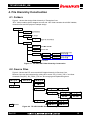
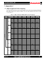
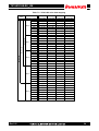
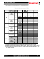
TIP-VBY1HS-RX_UM
User Manual
Preliminary
Preliminary
TIP-VBY1HS
Receiver Core
User Manual
V-by-One® HS Standard IP
for Xilinx FPGA
Rev.1.00
Tokyo Electron Device Ltd.
Rev1.00
1
TIP-VBY1HS-RX_UM
Revision History
The following table shows the revision history for this document.
Revision
Rev.1.0.0E
Rev1.00
Date
2010/04/12
Comments
First Release
2
TIP-VBY1HS-RX_UM
Table of Contents
1. Introduction ......................................................................................................................6
1.1. About the Core.................................................................................................... 6
1.2. Recommended Design Experience ....................................................................7
1.3. Additional Core Resources ................................................................................. 7
1.4. Technical Support............................................................................................... 7
1.5. References ......................................................................................................... 7
2. Core Architecture .............................................................................................................8
2.1. Block Diagram .................................................................................................... 8
2.2. Receiver Core Interfaces .................................................................................... 9
3. Clock Construction.........................................................................................................13
4. File Hierarchy Construction............................................................................................15
4.1. Folders.............................................................................................................. 15
4.2. Source Files...................................................................................................... 15
5. Parameterization............................................................................................................16
5.1. Wrapper File ..................................................................................................... 16
5.2. Constraint File................................................................................................... 20
6. Constraint the Core........................................................................................................21
6.1. Timing............................................................................................................... 21
6.2. Placement......................................................................................................... 22
7. Appendix-1.....................................................................................................................23
7.1. Byte length and Color mapping......................................................................... 23
7.2. Allocation of pixel to Data Lane ........................................................................ 25
8. Appendix-2.....................................................................................................................26
8.1. Reference clock ................................................................................................ 26
8.2. PLL configuration of Transceiver ...................................................................... 27
Rev1.00
3
TIP-VBY1HS-RX_UM
Schedule of Figures
Figure 2.1
Figure 2.2
Figure 2.3
Figure 3.1
Figure 3.2
Figure 4.1
Figure 4.2
Figure 7.1
Figure 8.1
Rev1.00
Receiver Core Top Level Block Diagram...........................................................8
User Data Interface Timing Chart....................................................................10
Control Data Active Term ................................................................................10
RX_PLL Construction......................................................................................13
RX_CLK_RST_GEN Construction ..................................................................14
TIP-VBY1HS Folder Hierarchy Construction ...................................................15
TD-BX1HSip-RX Source Hierarchy Construction ............................................15
Allocation of pixel to Data Lane .......................................................................25
Receiver FPGA Recommended Board Design................................................26
4
TIP-VBY1HS-RX_UM
Schedule of Tables
Table 2.1
Table 2.2
Table 2.3
Table 2.4
Table 2.5
Table 3.1
Table 3.2
Table 5.1
Table 5.2
Table 5.3
Table 7.1
Table 7.2
Table 8.1
Table 8.2
Table 8.3
Table 8.4
Table 8.5
Table 8.6
Rev1.00
General Use Signal Descriptions........................................................................9
Mode Setting Signal Descriptions.......................................................................9
User Data Interface Signal Descriptions...........................................................10
Transceiver Interface Signal Descriptions ........................................................11
Link Status Signal Descriptions ........................................................................12
RX_PLL Signal Descriptions.............................................................................13
RX_CLK_RST_GEN Signal Descriptions .........................................................14
Parameterization Table of Wrapper file ............................................................16
Byte mode Data Mapping .................................................................................16
Parameterization Table of UCF ........................................................................20
RGB / YCbCr444 / RGBW / RGBY color data mapping ...................................23
YCbCr422 color data mapping .........................................................................24
Virtex-6 GTX REFCLK Characteristics .............................................................26
Spartan-6 GTP REFCLK Characteristics..........................................................26
PLL Divider Attribute and Common Values ......................................................27
Virtex-6 GTX Transceiver Performance............................................................27
Spartan-6 GTP Transceiver Performance ........................................................27
Video data format vs. FPGA .............................................................................29
5
TIP-VBY1HS-RX_UM
1. Introduction
This chapter introduces the Tokyo Electron Device Ltd.(TED)’s Receiver Core that makes up
V-by-One® HS standard IP Core “TIP-VBY1HS” designed for Xilinx FPGAs. It also describes
design environment for development and provides other related information.
V-by-One® HS standard has been developed by THine Electronics,Inc. to offer capabilities for Flat
Panel Display (FPD) markets that are requiring ever-higher frame rates and higher resolutions.
This manual provides information about how to edit the TIP-VBY1HS Receiver Core‘s wrapper files
and constraint files, and so on.
1.1. About the Core
TIP-VBY1HS Receiver Core is a Soft IP designed for Verilog-HDL design environment. It can be
implemented in any suitable arrangement with User Logic for the following FPGA family.
・ Hardware Validation
The TIP-VBY1HS Core has acquired a connectivity certification from THine electronics, Inc. by
successfully completing a connectivity test between an FPGA board with the Core and a
V-by-One® HS evaluation board.
・ Target Device
Target devices of the TIP-VBY1HS Core include the Virtex-6 family with GTX Transceiver and
the Spartan-6 family with GTP Transceiver.
Note that dependent on FPGA transceiver specifications, the following constraints are imposed
on high-speed data lane’s transmission bandwidth that is provided by the transceiver.
- 600Mbps~3.75Gbps per data lane (same as the standard)
Virtex-6 LXT (XC6VxxxLXT) all speed grade
Virtex-6 SXT (XC6VxxxSXT) all speed grade
- 614Mbps~810Mbps, 1.2288Gbps~1.62Gbps, 2.457Gbps~3.125Gbps per data lane
Spartan-6 LXT (XC6SxxxLXT) speed grade -3, -4
speed grade -2 : Maximum rate is less than 2.7Gbps
Following equation shows how to determine the data rate of the lane (Gbps).
Example
Byte-mode = 4byte, Pixel Clock frequency = 148.5MHz, Number of data lanes = 2
Data rate per lane = ( 32bits × 148.5MHz × 1.25 ) / 2 = 2.97Gbps
Besides the above, there are other constraints and cautions that are attributed to FPGA
specifications and characteristics. For more information, refer to the relevant chapters of this
document and the FPGA data sheets.
Rev1.00
6
TIP-VBY1HS-RX_UM
1.2. Recommended Design Experience
The following development environments are required to develop TIP-VBY1HS Core.
- Implement : ISE® 11.4 Logic Edition and above
- Synthesis : Xilinx XST 11.4 and above
- Simulation : Mentor Graphics® ModelSim® 6.5a and above (for Verilog-HDL)
1.3. Additional Core Resources
Besides this document, the following support documentation is available.
- TIP-VBY1HS Data Sheet
- TIP-VBY1HS Transmitter Core User Manual
- TIP-VBY1HS Transceiver PLL Setting Estimate Sheet (Excel)
- TIP-VBY1HS CVK Reference Design User Manual
1.4. Technical Support
For technical support, go to [email protected]
Tokyo Electron Device Ltd. (TED) provides technical support for this IP Core when used as
described in the product documentation. TED cannot guarantee timing, functionality, or support of
product if implemented in devices that are not defined in the documentation, if customized beyond
that allowed in the product documentation.
TED also offers a contract-based development service for customized design or additional
function design (ex. more than 16 data lanes for Virtex-6).
1.5. References
The following V-by-One®HS Standard and FPGA documentations were referenced when
developing the TIP-VBY1HS.
- V-by-One®HS Standard Version 1.2 (Jan 15, 2009) by THine Electronics, Inc.
- Virtex-6 FPGA GTX Transceivers User Guide (UG366 v2.2 Feb 23, 2010)
- Virtex-6 FPGA Data Sheet : DC and Switching Characteristics (DS152 v2.2 Feb 9,2010)
- Spartan-6 FPGA GTP Transceivers User Guide (UG386 v2.1 Mar 30,2010)
- Spartan-6 FPGA Data Sheet : DC and Switching Characteristics (DS162 v1.4 Mar 10,2010)
Rev1.00
7
TIP-VBY1HS-RX_UM
2. Core Architecture
This chapter provides and overview of the TIP-VBY1HS Receiver Core architecture.
The TIP-VBY1HS is a full-featured soft IP core that is provided in the form of a NGC Netlist for
V-by-One® HS compliant components and a Verilog-RTL for other components.
2.1. Block Diagram
The Receiver Core is partitioned into three major blocks, as shown in Figure 2.1.
・ RX_LANE_X. Provides for the delivery of the video stream. This block contains major functional
blocks called RX_MAIN_LINKs based on the number of Data Lanes. Each RX_MAIN_LINK
has two Data Lanes (one Data Lane is valid in single Data Lane setting).
・ RX_DEFORMATTER. This block restores formatted data from the RX-LANE_X block and
outputs to User Logic.
・ RX_CLK_RST_GEN. This block generates all clocks needed for the above blocks.
FPGA
RX_VX1HS_TOP
RX_LANE_X
RX_DEFORMATTER
MGTREFCLK_P/N
AFIFO_F
(NGC Netlist)
LOCKN / HTPDN
RX_MAIN_LINK_0/1
RX0_P/N
(NGC Netlist)
RX1_P/N
s_LN_VSYNC[N-1:0]
EQ[2:0]
AFIFO_F
(NGC Netlist)
VSYNC
HSYNC
DE
s_LN0_HSYNC[N-1:0]
s_LN0_DE[N-1:0]
DI[39:0]
s_LN0_DI[N*40-1:0]
s_LN0_CTL[N*24-1:0]
CTL[23:0]
※N = Number of Data Lanes
RXn-1_P/N
RX_MAIN_LINK_n-1/n
(NGC Netlist)
RXn_P/N
FIELD_BET
FIELD_BET_CHK
LCLK
PXCLK
PXCLK
RXUSRCLK2
RXUSRCLK
RXRECCLK
FIELD_BET
(NGC Netlist)
PCLK
RX_PLL
RX_CLK_RST_GEN
PDN
Figure 2.1 Receiver Core Top Level Block Diagram
Rev1.00
8
TIP-VBY1HS-RX_UM
2.2. Receiver Core Interfaces
・ General Signals
Table 2.1 describes the General Use signals.
Table 2.1 General Use Signal Descriptions
Signal Name
PDN
Direction
Polarity
Input
‘L’
Description
Power Down
This signal clears all functional blocks.
・ Mode Setting Signals
Table 2.2 describes the Mode Setting signals.
Table 2.2 Mode Setting Signal Descriptions
Signal Name
FIELD_BET
Direction
Polarity
Input
‘H’
Description
Field BET Mode Enable
In the mode to check the quality of high-speed serial data lines, Field BET Mode enables
FIELD_BET input to receive a data pattern like BET (Bit Error Tester)from a transmitting device
in Field BET mode and validate it.
Rev1.00
9
TIP-VBY1HS-RX_UM
・ User Data Interface
Table 2.3 describes the User Data Interface signals.
Table 2.3 User Data Interface Signal Descriptions
Signal Name
Direction
Polarity
Description
PXCLK
Output
↑
Pixel Clock
VSYNC
Output
‘L’
Vertical sync pulse
HSYNC
Output
‘L’
Horizontal sync pulse
DE
Output
‘H’
Video data enable
DO [39:0]
Output
-
Video data
CTL [23:0]
Output
-
Control data
Figure 2.2 shows the timing chart of the User data interface.
Video data is output as effective pixel region when DE is High (active). On the other hand,
Control data is output as effective data region when DE is Low (inactive) excluding a period of
1cycle before and after that period. (Note that there are constraints on this effective period
dependent on number of lanes used. For more information, refer to the subsequent
description).
Figure 2.2 User Data Interface Timing Chart
As shown in Figure 2.3, as the number of data lanes increases, the effective period for Control
data is shortened since the ineffective period at both ends increases. This should be
considered when using Control data.
Figure 2.3 Control Data Active Term
Rev1.00
10
TIP-VBY1HS-RX_UM
・ Transceiver Interface
Table 2.4 describes the Transceiver Interface signals.
Table 2.4 Transceiver Interface Signal Descriptions
Signal Name
Direction
Polarity
Description
REFCLK_P0
Input
↑
REFCLK of GTX/GTP Transceiver Positive
REFCLK_N0
input
↑
REFCLK of GTX/GTP Transceiver Negative
REFCLK_P1
Input
↑
REFCLK of GTX/GTP Transceiver Positive (optional)
REFCLK_N1
Input
↑
REFCLK of GTX/GTP Transceiver Negative (optional)
RX0_P [n:0]
Input
-
High-speed serial Data Lanes positive
RX0_N [n:0]
Input
-
High-speed serial Data Lanes negative
CLKOUT
Output
↑
EQ [2:0]
Input
-
Recovery clock output to External PLL. (optional)
Equalizer Setting
・RX0_P/N [n:0] (n=0,1,3,7)
These are external pins of the FPGA for receiving the serial video data reception. Input pins of
Virtex-6 GTX Transceivers or Spartan-6 GTP Transceivers are used.
In the case of using the input pins of Spartan-6 GTP Transceiver, the RX_MAIN_LINK module
shown in Figure 2.1 Block Diagram (section 2.1 “Block Diagram”) is definitely mapped to a
single GTP_DUAL_Tile.
Two GTPs exist in GTP_DUAL_Tile. So, in the case of 1-Data Lane and 2-Data Lanes, one
GTP_DUAL_Tile should be used, in the case of 4-Data Lanes, two GTP_DUAL_Tiles should
be used, and in the case of 8-Data Lanes, four GTP_DUAL_Tiles should be used.
As for Virtex-6, there are no above constraints.
・REFCLK_P/N0, REFCLK_P/N1
Two external reference clock input pins are provided for Spartan-6 GTP Transceiver. They are
used to provide a clock to each GTP_DUAL_Tile on the top and bottom sides of FPGA. If only
either side of GTP_DUAL_Tile is used, it is not needed to have two clock pins.
For more information about GTP_DUAL_Tile, refer to the Spartan-6 FPGA GTP Transceivers
User Guide.
As for Virtex-6, there are no above constraints.
・EQ [3:0]
These signal pins are used to set Equalizer Control for RX0_P/N input. They correspond to
the following GTX/GTP port name:
EQ[2:0] = RXEQMIX[2:0]
(In case of GTP Transceiver, only EQ [1:0] is valid)
For characteristics corresponding to these setting values, refer to the associated FPGA
Transceiver User Guide and determine an appropriate value to match the characteristics of the
device and the transmission line to a transmission side.
Rev1.00
11
TIP-VBY1HS-RX_UM
・ Link Status Signals
Table 2.5 describes the Link Status signals.
Table 2.5 Link Status Signal Descriptions
Signal Name
Direction
Polarity
Description
HTPDN
Output
‘L’
Hot plug detect
LOCKN
Output
‘L’
Lock detect
FIELD_BET_CHK
Output
‘H’
Filed BET mode Check Error Status
・HTPDN
This is an external pin connecting to the equivalent output pin of a transmitting end device.
It notifies the transmitter side of that the receiving end device has been connected.
・LOCKN
This is an external pin connecting to the equivalent output pin of a transmitting end device.
It notifies the transmitter side of that the clock data recovery (CDR) of the receiving end device
has been locked.
・FIELD_BET_CHK
This notifies the result of checking in the Field BET mode (“H” in Error).
Rev1.00
12
TIP-VBY1HS-RX_UM
3. Clock Construction
Figure 3.1 shows the construction of the clock module – RX_PLL
Figure 3.1 RX_PLL Construction
Table 3.1 describes the RX_PLL signals.
About the connection of each clock, refer to the Figure 2.1 Top Level Block Diagram.
Table 3.1 RX_PLL Signal Descriptions
Signal Name
Direction
Polarity
RXRECCLK
Input
↑
GTPPLLLKDET
input
‘H’
RXUSRCLK
Output
↑
Clock to “RXUSRCLK” port of GTP/GTX and parallel
clock for “RX_MAIN_LINK” internal logic
RXUSRCLK2
Output
↑
Clock to “RXUSRCLK2” port of GTP/GTX
RX_PLL_LOCKED
Output
↑
PLL locked signal
Rev1.00
Description
Recovery clock from GTP/GTX
Locked signal from “PLLLKDET” port of GTP/GTX
13
TIP-VBY1HS-RX_UM
Figure 3.2 shows the construction of the clock module – RX_CLK_RST_GEN.
Figure 3.2 RX_CLK_RST_GEN Construction
Table 3.2 describes the RX_CLK_RST_GEN signals.
About the connection of each clock, refer to the Figure 2.1 Top Level Block Diagram.
Table 3.2 RX_CLK_RST_GEN Signal Descriptions
Signal Name
Direction
Polarity
PCLK
Input
↑
RX_PLL_LOCKED
input
‘H’
PLL locked signal from “RX_PLL” module
HTPDN [n-1:0]
input
‘H’
Hot Plug Detect internal signal from RX_MAIN_LINKs
PDN
input
‘L’
Power Down
PXCLK
Output
↑
Pixel clock for User Data Interface
LCLK
Output
↑
Lane clock for adjustment of the signal rate between
“RX_MAIN_LINK” and “RX_DEFORMATTER”
RX_PLL_LOCKED
Output
‘L’
Locked signal of all PLLs
GTPRESET
Output
‘H’
Reset for GTP/GTX
Rev1.00
Description
Parallel clock (RXUSRCLK) from “RX_PLL” module
14
TIP-VBY1HS-RX_UM
4. File Hierarchy Construction
4.1. Folders
Figure 4.1 shows the design folder hierarchy in Transmitter Core.
“RTL” folder contains the all wrapper sources and “ISE” folder contains the all NGC Netlists,
constraint files and ISE project of sample design.
Figure 4.1 TIP-VBY1HS Folder Hierarchy Construction
4.2. Source Files
Figure 4.2 shows the RTL source and NGC Netlist hierarchy in Receiver Core.
Receiver Core can be customized by editing RTL source-”RX_VX1HS_TOP.v” and User
Constraint File(UCF) -RX_FPGA_TOP.ucf, and merging and implementing them.
Figure 4.2 TIP-VBY1HS-RX Source Hierarchy Construction
Rev1.00
15
TIP-VBY1HS-RX_UM
5. Parameterization
5.1. Wrapper File
“RX_VX1HS_TOP.v” is a wrapper file that can be regarded as a single hierarchy or used by
merging it into the top hierarchy of user logic.
Table 5.1 shows the parameters that are defined in the wrapper file – RX_VX1HS_TOP.v.
Table 5.1 Parameterization Table of Wrapper file
Parameter Name
Values
P_FPGA_TYPE
0,1
P_LANE_NUM
1,2,4,8
Description
Select the target FPGA
0: Virtex-6
1: Spartan-6
Number of high-speed serial data lanes
P_BYTE_MD
3,4,5
Byte width of video data and control signal
P_REFCLK_PERIOD
real
Period of the REFCLK frequency
P_RXRECCLK_PERIOD
integer
Multiplication rate of the RXRECCLK reference PLL output
P_RXRECCLK_MULT
integer
Multiplication rate of the RXRECCLK reference PLL output
P_RXRECCLK_DIVIDE
integer
Division rate of the RXRECCLK reference PLL output
P_PCLK_PERIOD
real
Period of the PCLK frequency
P_PCLK_MULT
integer
Multiplication rate of the PCLK reference PLL output
P_PCLK_DIVIDE
integer
Division rate of the PCLK reference PLL output
parameter
P_FPGA_TYPE
// 1:Spartan6, 0:Virtex6
= integer ,
This parameter is used to select a target FPGA type.
Based on this parameter, a dedicated module for Virtex-6 or Spartan-6 is called in the merge
routine.
parameter
P_LANE_NUM
= integer ,
// TX Lane Number : 1,2,4,8
This parameter is used to set the number of Data Lanes.
parameter
P_BYTE_MD
= integer ,
// Byte mode : 3,4,5
This parameter is used to set Byte Mode for user data interface.
Table 5.2 provides a mapping table between Byte Mode setting and DO/CTL output effective bit
width.
Table 5.2 Byte mode Data Mapping
P_BYTE_MD
DO [39:0]
3
23:0
4
5
Rev1.00
CTL [23:0]
7:0
31:0
39:0
15:0
23:0
16
TIP-VBY1HS-RX_UM
parameter
P_REFCLK_PERIOD = real ,
// MGT Reference clock Period
This parameter is used to set frequency period of a REFCLK that is input as a reference clock
for the GTP/GTX Transceiver.
parameter
P_RXRECCLK_PERIOD = real ,
// RXRECCLK Period
This parameter is used to set frequency period of the recovery clock that is output from the
GTP/GTX Transceiver. This value can be calculated by following equation.
(Refer to chapter 5.2 ”Constraint File” about PLL_DIVSEL_*** parameter )
for Virtex-6
for Spartan-6
Example
Pixel clock Period = 6.734ns (148.5MHz), 4 byte mode, 2 data lanes for Spartan-6
PLL_DIVSEL_REF = 1, PLL_DIVSEL_FB = 2, PLL_DIVSEL_OUT = 1
RXRECCLK_PERIOD = 6.734 / (4 * 8) / 1.25 * 2 / 1 / 1 * (2 * 5) = 3.367
parameter
parameter
P_RXRECCLK_MULT = integer , // RXRECCLK PLL MULT
P_RXRECCLK_DIVIDE = integer , // RXRECCLK PLL DIVCLK_DIVIDE
This parameter is used to set frequency multiplication and dividing ratio of PLL (Figure 3.1) that
generates an internal clock from the recovery clock(RXRECCLK) output of the GTP/GTX
Transceiver in the MAIN_LINK block. These values should be observed the following rules
Example
RXRECCLK frequency = 297MHz for Virtex-6
PLL_DIVSEL_REF = 1, PLL_DIVSEL_FB = 2, PLL_DIVSEL_OUT = 1
600MHz < 297MHz * P_RXRECCLK_MULT / P_RXRECCLK_DIVIDE < 1200MHz
1 * 1 * P_RXRECCLK_MULT / (2 * P_RXRECCLK_DIVIDE) = must be integer 1~128
P_RXRECCLK_MULT = 4
P_RXRECCLK_DIVIDE = 1
Rev1.00
17
TIP-VBY1HS-RX_UM
parameter
P_PCLK_PERIOD = real ,
// PCLK Period
This parameter is used to set frequency period of PCLK input of Figure 3.2 (RXUSRCLK from
RX_PLL of Figure 3.1 )
This value can be calculated the following equation.
Example
Pixel Clock period = 6.734ns (148.5MHz), Number of data lanes = 2, Byte-mode = 4byte
6.734 * 2 / 4 = 3.367 ns
parameter
parameter
P_PCLK_MULT = integer ,
P_PCLK_DIVIDE = integer ,
// PCLK_MULT
// PCLK_DIVIDE
This parameter is used to set frequency multiplication and dividing ratio of the PLL (Figure 3.2)
that generates an internal clock from the PCLK (RXUSRCLK from RX_PLL) input.
These values should be observed the following rule.(Depending on the VCO specification.)
( In the case of Spartan-6, the value in ( ) is corresponded. )
Example
PCLK frequency = 297MHz
for Spartan-6
400MHz < 297MHz * P_PCLK_MULT / P_PCLK_DIVIDE < 1000MHz
P_PCLK_MULT = 2 (or 3) P_PCLK_DIVIDE = 1
※) Parameter of “RX_CLK_RST_GEN” module
Although the RX_CLK_RST_GEN includes the following parameters to set the dividing values
of PLL outputs for all combinations of the byte mode and number of Data Lanes, more simple
constitution that makes an appropriate frequency for “PXCLK” and “LCLK” would be acceptable.
These dividing values should be observed the following rules.
Example
// P_PCLK_MULT = 4 ( = 8 in the case of P_NUM_LANE = 8), P_PCLK_DIVIDE = 1
parameter P_3BYTE_PXCLK_DIVIDE
= ( P_LANE_NUM == 1 ) ? 12 :
( P_LANE_NUM == 2 ) ? 6 :
( P_LANE_NUM == 4 ) ? 3 : 3 ;
parameter P_4BYTE_PXCLK_DIVIDE
= ( P_LANE_NUM == 1 ) ? 16 :
( P_LANE_NUM == 2 ) ? 8 :
( P_LANE_NUM == 4 ) ? 4 : 4 ;
parameter P_5BYTE_PXCLK_DIVIDE
= ( P_LANE_NUM == 1 ) ? 20 :
( P_LANE_NUM == 2 ) ? 10 :
( P_LANE_NUM == 4 ) ? 5 : 5 ;
// P_PCLK_MULT = 4 ( = 8 in the case of P_NUM_LANE = 8), P_PCLK_DIVIDE = 1
parameter P_3BYTE_LCLK_DIVIDE
= ( P_LANE_NUM == 8 ) ? 24 : 12 ;
parameter P_4BYTE_LCLK_DIVIDE
= ( P_LANE_NUM == 8 ) ? 32 : 16 ;
parameter P_5BYTE_LCLK_DIVIDE
= ( P_LANE_NUM == 8 ) ? 40 : 20 ;
Rev1.00
18
TIP-VBY1HS-RX_UM
// Simulation attributes
parameter
P_SIMSPEEDUP
=0,
// Set to 1 for speed up sim reset
parameter
P_SIMULATION
=0,
// Set to 1 for simulation
These parameters are set to “1” for RTL Simulation.
Set “0” for Normal Merging.
Rev1.00
19
TIP-VBY1HS-RX_UM
5.2. Constraint File
A constraint file, RX_VX1HS_TOP.ucf, also contains some important parameters.
Table 5.3 shows the parameterization that can be defined within the User Constraint File–
RX_VX1HS_TOP.ucf.
Table 5.3 Parameterization Table of UCF
Parameter Name
Values
Description
P_PLL_DIVSEL_REF
1,2
PLL Reference clock input Divider of GTX/GTP Transceiver
P_PLL_DIVSEL_FB
P_PLL_DIVSEL_OUT
1,2,4,5
1,2,4
PLL Feedback Dividers of GTX/GTP Transceiver
PLL Output Divider of GTX/GTP Transceiver
These parameter settings have a close relation with device specifications and characteristics of
Virtex-6 (GTX) and Spartan-6 (GTP).
For more information about the meaning and the effectiveness of these setting values, refer to
Chapter 8.2 of this document.
The attached TIP-VBY1HS Transceiver PLL Settings Estimate Sheet (Exel Sheet) is helpful for
calculating a setting value.
(It is important to understand the basic idea of these parameters before calculating a setting
value)
Rev1.00
20
TIP-VBY1HS-RX_UM
6. Constraint the Core
A constraint file, RX_VX1HS_TOP.ucf, contains placement and timing constraints of major
dedicated blocks.
It is needed to enter RX_VX1HS_TOP.ucf directly as a constraint file with the same hierarchy with
RX_VX1HS_TOP.v or load it into a constraint file for the top hierarchy of User Logic on ISE.
6.1. Timing
The following are the timing constraints on clocks associated with the TIP-VBY1HS Receiver Core
in the case of 4 byte-mode, 148.5MHz pixel clock frequency, 2-Data Lanes.
To make explanation plain, the constraint values are matched with real movement speed. So the
value with the margin is recommended in the development.
## Generating the clock groups and period constraints for each clock domain. ##
## Recovery clock
NET "*RXRECCLK" TNM_NET = "TN_RXRECCLK" ;
TIMESPEC "TS_RXRECCLK" = PERIOD "TN_RXRECCLK" 3.367ns HIGH 50 % ;
## RXUSRCLK
RXUSRCLK for GTP/GTX ( = RXRECCLK period)
NET "*RXUSRCLK" TNM_NET = "TN_RXUSRCLK" ;
TIMESPEC "TS_RXUSRCLK" = PERIOD "TN_RXUSRCLK" 3.367ns HIGH 50 % ;
## RXUSRCLK2
RXUSRCLK2 for GTP/GTX ( = RXRECCLK period * 2)
NET "*RXUSRCLK2" TNM_NET = "TN_RXUSRCLK2";
TIMESPEC
TIMESPEC "TS_RXUSRCLK2" = PERIOD "TN_RXUSRCLK2" 6.734ns HIGH 50 % ;
## Pixel clock
NET "*PXCLK" TNM_NET = "TN_PXCLK" ;
TIMESPEC "TS_PXCLK" = PERIOD "TN_PXCLK" 6.734ns HIGH 50 % ;
## Lane clock
NET "*LCLK" TNM_NET = "TN_LCLK" ;
TIMESPEC "TS_LCLK" = PERIOD "TN_LCLK"
"TN_LCLK" 13.468ns HIGH 50 % ;
##
## Data Path Constraints between the other clock domains ##
TIMESPEC "TS_RXUSRCLK_2_RXUSRCLK2" = FROM "TN_RXUSRCLK" TO "TN_RXUSRCLK2"
"TN_RXUSRCLK2" 5.000ns ;
TIMESPEC "TS_RXUSRCLK2_2_RXUSRCLK" = FROM "TN_RXUSRCLK2" TO "TN_RXUSRCLK"
"TN_RXUSRCLK" 5.000ns ;
TIMESPEC "TS_RXUSRCLK_2_LCLK" = FROM "TN_RXUSRCLK" TO "TN_LCLK" 5.000ns ;
TIMESPEC "TS_LCLK_2_RXUSRCLK" = FROM "TN_LCLK" TO "TN_RXUSRCLK" 5.000ns ;
TIMESPEC "TS_PXCLK_2_LCLK" = FROM "TN_PXCLK" TO "TN_LCLK" 5.000ns ;
TIMESPEC "TS_LCLK_2_PXCLK"
"TS_LCLK_2_PXCLK" = FROM "TN_LCLK" TO "TN_PXCLK" 5.000ns ;
##
## Timing Ignore ##
INST "*r_HTPDN*" TNM = "TN_HTPDN" ;
INST "*r_LOCKN*" TNM = "TN_LOCKN" ;
INST "*r_FIELD_BET_ERR*" TNM = "TN_FIELDBET" ;
TIMESPEC "TS_HTPDN_TIG" = FROM "TN_HTPDN" TO "TN_HTPDN" TIG ;
TIMESPEC "TS_LOCKN_TIG" = FROM "TN_LOCKN" TO "TN_LOCKN" TIG ;
TIMESPEC "TS_FIELDBET" = FROM "FFs" TO "TN_FIELDBET" TIG ;
Rev1.00
21
TIP-VBY1HS-RX_UM
6.2. Placement
The following is a placement constraint for Virtex-6 GTX Transceiver.
These positions are only an example, so it should be changed according with the GTX port to use.
## Placement for GTX of Data Lane - 0
INST "* U_R
U_RX_MAIN_LINK01
X_MAIN_LINK01*
01*/*U_R
U_RX_GTX_WRAP0
X_GTX_WRAP0*/gtx0_
/gtx0_r
0_rx_gtx_wrap_i/
x_gtx_wrap_i/gtxe1_i " LOC = GTXE1_X0Y0 ;
## Placement for GTX of Data Lane - 1
INST "* U_R
U_RX_MAIN_LINK01
X_MAIN_LINK01*
01*/*U_R
U_RX_GTX_WRAP1
X_GTX_WRAP1*/gtx0_r
/gtx0_rx_gtx_wrap_i/
x_gtx_wrap_i/gtxe1_i " LOC = GTXE1_X0Y1 ;
## Placement for GTX of Data Lane - 2
INST "* U_R
U_RX_MAIN_LINK32
X_MAIN_LINK32*
32*/*U_R
*U_RX_GTX_WRAP0
X_GTX_WRAP0*/gtx0_
*/gtx0_r
tx0_rx_gtx_wrap_i/
x_gtx_wrap_i/gtxe1_i " LOC = GTXE1_X0Y2 ;
## Placement for GTX of Data Lane - 3
INST "* U_R
U_RX_MAIN_LINK32
X_MAIN_LINK32*
32*/*U_R
*U_RX_GTX_WRAP1
X_GTX_WRAP1*/gtx0_r
*/gtx0_rx_gtx_wrap_i/
x_gtx_wrap_i/gtxe1_i " LOC = GTXE1_X0Y3 ;
## Placement for GTX of Data Lane - 4
INST "* U_R
U_RX_MAIN_LINK54
X_MAIN_LINK54*
54*/*U_R
*U_RX_GTX_WRAP0
X_GTX_WRAP0*/gtx0_r
/gtx0_rx_gtx_wrap_i/
x_gtx_wrap_i/gtxe1_i " LOC = GTXE1_X0Y4 ;
## Placement for GTX of Data Lane - 5
INST "* U_R
U_RX_MAIN_LINK54
X_MAIN_LINK54*
54*/*U_R
*U_RX_GTX_WRAP1
X_GTX_WRAP1*/gtx0_r
*/gtx0_rx_gtx_wrap_i/
x_gtx_wrap_i/gtxe1_i " LOC = GTXE1_X0Y5 ;
## Placement for GTX of Data Lane - 6
INST "* U_R
U_RX_MAIN_LINK76
X_MAIN_LINK76*
76*/*U_R
*U_RX_GTX_WRAP0
X_GTX_WRAP0*/gtx0_r
*/gtx0_rx_gtx_wrap_i/
x_gtx_wrap_i/gtxe1_i " LOC = GTXE1_X0Y6 ;
## Placement for GTX of Data Lane - 7
INST "* U_R
U_RX_MAIN_LINK76
X_MAIN_LINK76*
76*/*U_R
*U_RX_GTX_WRAP1
X_GTX_WRAP1*/gtx0_r
*/gtx0_rx_gtx_wrap_i/
x_gtx_wrap_i/gtxe1_i " LOC = GTXE1_X0Y7 ;
The following is a placement constraint for Spartan-6 GTP Transceiver.
These positions are only an example, so it should be changed according with the GTP port to use.
## Placement for GTP of Data Lanes – 0, 1
INST "* U_R
U_RX_MAIN_LINK01
X_MAIN_LINK01*
01*/tile0_r
/tile0_rx_gtp_wrap_i/gtpa1_dual_i
x_gtp_wrap_i/gtpa1_dual_i "
## Placement for GTP of Data Lanes – 2, 3
INST "*
"* U_R
U_RX_MAIN_LINK32
X_MAIN_LINK32*
32*/tile0_
/tile0_r
le0_rx_gtp_wrap_i/gtpa1_dual_i"
## Placement for GTP of Data Lanes – 4, 5
INST "*
"* U_R
U_RX_MAIN_LINK54
X_MAIN_LINK54*
54*/tile0_r
/tile0_rx_gtp_wrap_i/gtpa1_dual_i"
x_gtp_wrap_i/gtpa1_dual_i"
## Placement for GTP of Data Lanes – 6, 7
INST "*
"* U_R
U_RX_MAIN_LINK76
X_MAIN_LINK76*
76*/tile0_r
/tile0_rx_gtp_wrap_i/gtpa1_dual_i"
LOC = GTPA1_DUAL_X0
GTPA1_DUAL_X0Y0 ;
LOC = GTPA1_DUAL_X1
GTPA1_DUAL_X1Y0 ;
LOC = GTPA1_DUAL_X0
GTPA1_DUAL_X0Y1 ;
LOC = GTPA1_DUAL_X1
GTPA1_DUAL_X1Y1 ;
The contents mentioned above are the constraints necessary to a minimum.
So it is also recommended to add appropriate placement constraints to clock sources such as PLL,
BUFG and BUFIO2 at a good balance with the user logic.
Rev1.00
22
TIP-VBY1HS-RX_UM
7. Appendix-1
7.1. Byte length and Color mapping
The V-by-One® HS can be used to various types of color video format allocating D[39:0] to
pixel data in packer and un-packer mapping. The color data mapping should refer to Table
7.1 and Table 7.2.
Table 7.1 RGB / YCbCr444 / RGBW / RGBY color data mapping
Packer input &
Unpacker output
D[0]
D[1]
D[2]
D[3]
Byte0
D[4]
D[5]
D[6]
D[7]
36bpp RGB
/YCbCr444
R/Cr[4]
R/Cr[5]
R/Cr[6]
R/Cr[7]
R/Cr[8]
R/Cr[9]
R/Cr[10]
R/Cr[11]
30bpp RGB
/YCbCr444
R/Cr[2]
R/Cr[3]
R/Cr[4]
R/Cr[5]
R/Cr[6]
R/Cr[7]
R/Cr[8]
R/Cr[9]
24bpp RGB
/YCbCr444
R/Cr[0]
R/Cr[1]
R/Cr[2]
R/Cr[3]
R/Cr[4]
R/Cr[5]
R/Cr[6]
R/Cr[7]
18bpp RGB
/YCbCr444
R/Cr[0]
R/Cr[1]
R/Cr[2]
R/Cr[3]
R/Cr[4]
R/Cr[5]
40bpp RGBW
/RGBY
R[2]
R[3]
R[4]
R[5]
R[6]
R[7]
R[8]
R[9]
32bpp RGBW
/RGBY
R[0]
R[1]
R[2]
R[3]
R[4]
R[5]
R[6]
R[7]
Byte1
D[8]
D[9]
D[10]
D[11]
D[12]
D[13]
D[14]
D[15]
G/Y[4]
G/Y[5]
G/Y[6]
G/Y[7]
G/Y[8]
G/Y[9]
G/Y[10]
G/Y[11]
G/Y[2]
G/Y[3]
G/Y[4]
G/Y[5]
G/Y[6]
G/Y[7]
G/Y[8]
G/Y[9]
G/Y[0]
G/Y[1]
G/Y[2]
G/Y[3]
G/Y[4]
G/Y[5]
G/Y[6]
G/Y[7]
G/Y[0]
G/Y[1]
G/Y[2]
G/Y[3]
G/Y[4]
G/Y[5]
G[2]
G[3]
G[4]
G[5]
G[6]
G[7]
G[8]
G[9]
G[0]
G[1]
G[2]
G[3]
G[4]
G[5]
G[6]
G[7]
Byte2
D[16]
D[17]
D[18]
D[19]
D[20]
D[21]
D[22]
D[23]
B/Cb[4]
B/Cb[5]
B/Cb[6]
B/Cb[7]
B/Cb[8]
B/Cb[9]
B/Cb[10]
B/Cb[11]
B/Cb[2]
B/Cb[3]
B/Cb[4]
B/Cb[5]
B/Cb[6]
B/Cb[7]
B/Cb[8]
B/Cb[9]
B/Cb[0]
B/Cb[1]
B/Cb[2]
B/Cb[3]
B/Cb[4]
B/Cb[5]
B/Cb[6]
B/Cb[7]
B/Cb[0]
B/Cb[1]
B/Cb[2]
B/Cb[3]
B/Cb[4]
B/Cb[5]
B[2]
B[3]
B[4]
B[5]
B[6]
B[7]
B[8]
B[9]
B[0]
B[1]
B[2]
B[3]
B[4]
B[5]
B[6]
B[7]
Byte3
D[24]
D[25]
D[26]
D[27]
D[28]
D[29]
D[30]
D[31]
B/Cb[2]
B/Cb[3]
G/Y[2]
G/Y[3]
R/Cr[2]
R/Cr[3]
B/Cb[0]
B/Cb[1]
G/Y[0]
G/Y[1]
R/Cr[0]
R/Cr[1]
-
-
R[0]
R[1]
G[0]
G[1]
B[0]
B[1]
W/Y[0]
W/Y[1]
-
Byte4
D[32]
D[33]
D[34]
D[35]
D[36]
D[37]
D[38]
D[39]
B/Cb[0]
B/Cb[1]
G/Y[0]
G/Y[1]
R/Cr[0]
R/Cr[1]
-
-
-
W/Y[2]
W/Y[3]
W/Y[4]
W/Y[5]
W/Y[6]
W/Y[7]
W/Y[8]
W/Y[9]
W/Y[0]
W/Y[1]
W/Y[2]
W/Y[3]
W/Y[4]
W/Y[5]
W/Y[6]
W/Y[7]
5byte mode
4byte mode
3byte mode
Mode
Rev1.00
23
TIP-VBY1HS-RX_UM
Table 7.2 YCbCr422 color data mapping
Packer input &
Unpacker output
D[0]
D[1]
D[2]
D[3]
Byte0
D[4]
D[5]
D[6]
D[7]
32bpp
/YCbCr422
Cb/Cr[8]
Cb/Cr[9]
Cb/Cr[10]
Cb/Cr[11]
Cb/Cr[12]
Cb/Cr[13]
Cb/Cr[14]
Cb/Cr[15]
24bpp
/YCbCr422
Cb/Cr[4]
Cb/Cr[5]
Cb/Cr[6]
Cb/Cr[7]
Cb/Cr[8]
Cb/Cr[9]
Cb/Cr[10]
Cb/Cr[11]
20bpp
/YCbCr422
Cb/Cr[2]
Cb/Cr[3]
Cb/Cr[4]
Cb/Cr[5]
Cb/Cr[6]
Cb/Cr[7]
Cb/Cr[8]
Cb/Cr[9]
16bpp
/YCbCr422
Cb/Cr[0]
Cb/Cr[1]
Cb/Cr[2]
Cb/Cr[3]
Cb/Cr[4]
Cb/Cr[5]
Cb/Cr[6]
Cb/Cr[7]
Byte1
D[8]
D[9]
D[10]
D[11]
D[12]
D[13]
D[14]
D[15]
Y[8]
Y[9]
Y[10]
Y[11]
Y[12]
Y[13]
Y[14]
Y[15]
Y[4]
Y[5]
Y[6]
Y[7]
Y[8]
Y[9]
Y[10]
Y[11]
Y[2]
Y[3]
Y[4]
Y[5]
Y[6]
Y[7]
Y[8]
Y[9]
Y[0]
Y[1]
Y[2]
Y[3]
Y[4]
Y[5]
Y[6]
Y[7]
Byte2
D[16]
D[17]
D[18]
D[19]
D[20]
D[21]
D[22]
D[23]
-
-
-
-
D[24]
Y[2]
-
-
-
D[25]
Y[3]
-
-
-
D[26]
Cb/Cr[2]
-
-
-
D[27]
Cb/Cr[3]
-
-
-
D[28]
Y[6]
Y[2]
Y[0]
-
5byte mode
4byte mode
3byte mode
Mode
Byte3
Byte4
Rev1.00
D[29]
Y[7]
Y[3]
Y[1]
-
D[30]
Cb/Cr[6]
Cb/Cr[2]
Cb/Cr[0]
-
D[31]
Cb/Cr[7]
Cb/Cr[3]
Cb/Cr[1]
-
D[32]
Y[0]
-
-
-
D[33]
Y[1]
-
-
-
D[34]
Cb/Cr[0]
-
-
-
D[35]
Cb/Cr[1]
-
-
-
D[36]
Y[4]
Y[0]
-
-
D[37]
Y[5]
Y[1]
-
-
D[38]
Cb/Cr[4]
Cb/Cr[0]
-
-
D[39]
Cb/Cr[5]
Cb/Cr[1]
-
-
24
TIP-VBY1HS-RX_UM
7.2. Allocation of pixel to Data Lane
Depend on the data rate and pixel color depth, it is permitted to increase the Data Lanes.
About the multiple Data Lanes combination, Refers to Figure 7.1.
The V-by-One® HS compliant components must be implemented with at least one Data Lane.
If the data rate of the required color depth and timing is higher than the components
maximum supported data rate, additional Data Lane can be used. (The maximum data rate
of V-by-One® HS Data Lane is 3.75Gbps per lane.) In this case, total lane count should be
even number, under the condition of the fewer lane number.
The pixel number for the horizontal active and blanking term (H-active, H-blank) should be
adjusted to become the multiple number of the lane count.
Blank
Line 1
Blank
Line 2
|
|
|
|
|
|
Lane 1
Lane 2
Lane 3
・
FSBS
FSBP
FSBE_SR
Pixel 1
Pixel N+1
・
・
・
FSBS
FSBP
FSBE
Pixel 1
Pixel N+1
・
・
・
FSBS
|
|
|
FSBE_SR
・
FSBS
FSBP
FSBE_SR
Pixel 2
Pixel N+2
・
・
・
FSBS
FSBP
FSBE
Pixel 2
Pixel N+2
・
・
・
FSBS
|
|
|
FSBE_SR
・
FSBS
FSBP
FSBE_SR
Pixel 3
Pixel N+3
・
・
・
FSBS
FSBP
FSBE
Pixel 3
Pixel N+3
・
・
・
FSBS
|
|
|
FSBE_SR
・・・
・・・
・・・
・・・
・・・
・・・
・・・
・・・
・・・
・・・
・・・
・・・
・・・
・・・
・・・
・・・
・・・
・・・
・・・
・・・
・・・
・・・
・・・
Lane N
・
FSBS
FSBP
FSBE_SR
Pixel N
Pixel 2N
・
・
・
FSBS
FSBP
FSBE
Pixel N
Pixel 2N
・
・
・
FSBS
|
|
|
FSBE_SR
Blanking Start
Blanking Payload
Blanking End & System Reset
Blanking End
Figure 7.1 Allocation of pixel to Data Lane
Rev1.00
25
TIP-VBY1HS-RX_UM
8. Appendix-2
8.1. Reference clock
When GTX/GTP Transceiver requires the different frequency reference clock to the pixel
clock, transmitter side requires the external PLL to generate the REFCLK.
In addition, REFCLK is recommended to be supplied by the exclusive differential port and to
be satisfied the specification shown in Table 8.1 and Table 8.2.
Table 8.1 Virtex-6 GTX REFCLK Characteristics
Symbol
FGCLK
TDCREF
Rxppmtol
Description
Reference clock frequency range
Reference clock duty cycle
Data/REFCLK PPM offset tolerance
Min
62.5
45
-200
Typ
50
-
Max
650
55
200
Units
MHz
%
ppm
Max
160
55
200
Units
ps
%
ppm
Table 8.2 Spartan-6 GTP REFCLK Characteristics
Symbol
Jitter
TDCREF
Rxppmtol
Description
Reference clock Jitter tolerance
Reference clock duty cycle
Data/REFCLK PPM offset tolerance
Min
60
45
-200
Typ
50
-
Figure 8.1 shows the construction of the Receiver FPGA board.
In addition to the same purpose as the Transmitter side, the Receiver side has the external VCXO
PLL IC to generate the initial REFCLK of the frequency that is required for the Clock Data
Recovery (CDR) of the GTP/GTX Transceivers. After CDR is locked, this VCXO PLL should be
phase-locked to the recovery clock and generate the REFCLK of frequency that is completely the
same as the Transmitter side.
Figure 8.1 Receiver FPGA Recommended Board Design
Rev1.00
26
TIP-VBY1HS-RX_UM
8.2. PLL configuration of Transceiver
To make the Reference Clock (MGTREFCLK) of the GTX/GTP transceiver equal to the Pixel
clock of the V-by-One® HS standard, this core requires the tuning of transceiver’s PLL
settings in the relation to the Byte-mode, and should have the limitation of clock rate
according to the transceiver’s specification.
Equation 8.1 shows how to determine the PLL output frequency (GHz).
Fpllclkin means the frequency of the Reference Clock.
Equation 8.1
Equation 8.2 shows how to determine the line rate (Gbps).
Equation 8.2
Table 8.3 shows the actual attribute and commonly used divider values.
Table 8.3 PLL Divider Attribute and Common Values
Factor
Attribute Name
Valid Settings
M
TXPLL_DIVSEL_REF
RXPLL_DIVSEL_REF
1, 2
N1
TXPLL_DIVSEL45_FB
RXPLL_DIVSEL45_FB
4, 5 (1)
N2
TXPLL_DIVSEL_FB
RXPLL_DIVSEL_FB
D
TXPLL_DIVSEL_OUT
RXPLL_DIVSEL_OUT
1, 2, 4, 5
1, 2, 4
(1) DIVSEL45_FB = 5 when INTDATAWIDTH is High (10bit mode) for 8B/10B encoding.
Table 8.4 and Table 8.5 show the GTX/GTP Transceiver Performance.
Table 8.4 Virtex-6 GTX Transceiver Performance
Symbol
Description
FGTPMAX
FGPLL
Maximum GTP Transceiver data rate
PLL frequency range
FGCLK
Reference clock frequency range
-3
Speed Grade
-2
6.5
6.5
1.2~3.3
Units
-1
5.0
1.2~2.7
Gbps
GHz
MHz
62.5~650
Table 8.5 Spartan-6 GTP Transceiver Performance
Symbol
FGTPMAX
FGPLL
FGCLK
Rev1.00
Description
Maximum GTP Transceiver data rate
PLL frequency range
Reference clock frequency range
Speed Grade
Units
-3
-2
3.125
2.7
1.2~1.62
60~160
Gbps
GHz
MHz
27
TIP-VBY1HS-RX_UM
Example
Byte-mode = 4byte, Pixel Clock frequency = 148.5MHz, No. of Data Lanes = 2
Data rate = ( 32bit * 148.5MHz * 1.25 ) / 2 = 2.97bps
- Virtex-6 GTX peed grade -2
M = 1, N1 = 5 (must be this value), N2 = 4,
Fpllclkout = 148.5MHz × 5 × 4 = 2.97GHz (1.2~3.3GHz)
D = 2,
Flinerate = ( 2.97GHz × 2 ) / 2 = 2.97Gbps (~3.75Gbps)
- Spartan-6 GTP speed grade -3
M = 1, N1 = 5 (must be this value), N2 = 2,
Fpllclkout = 148.5MHz × 5 × 2 = 1.485GHz (1.2~1.62GHz)
D = 1,
Flinerate = ( 1.485GHz × 2 ) / 1 = 2.97Gbps
(614Mbps~810Mbps, 1.2288Gbps~1.62Gbps, 2.457Gbps~3.125Gbps)
Rev1.00
28
TIP-VBY1HS-RX_UM
Table 8.6 shows the correspondence list for the video data formats.
Table 8.6 Video data format vs. FPGA
Resolution
Refresh rate
(Pixel Clock)
No of
Lane
Color depth
18/24 bit
60Hz
(74.25MHz)
1
30 bit
36 bit
18/24 bit
HD
120Hz
(148.5MHz)
2
30 bit
36 bit
18/24 bit
240Hz
(297MHz)
4
30 bit
36 bit
18/24 bit
60Hz
(148.5MHz)
2
30 bit
36 bit
18/24 bit
Full-HD
120Hz
(297MHz)
4
30 bit
36 bit
18/24 bit
240Hz
(594MHz)
8
30 bit
36 bit
8
18/24 bit
30 bit
36 bit
120Hz
(1188MHz)
16
18/24 bit
30 bit
36 bit
240Hz
(2376MHz)
32
18/24 bit
30 bit
36 bit
60Hz (594MHz)
4Kx2K
GTX
VirtexVirtex-6
GTP
Spartan-6
sp -3
✔(1)
✔
✔
✔(1)
✔
✔
✔(1)
✔
✔
✔(1)
✔
✔
✔(1)
✔
✔
✔(1)
✔
✔
✔(1)
✔
✔
(3)
✔
GTP
Spartan-6
sp -2
(3)
✔(2)
(3)
✔
(3)
✔(2)
(3)
✔
(3)
✔(2)
(3)
✔
(3)
✔(2)
(3)
✔
(3)
✔(2)
(3)
✔
(3)
✔(2)
(3)
✔
✔(2)
(1) Frequency of the GTX's REFCLK should not be integer dividing ratio to the pixel clock ones.
(2) Requires the double number of Data lanes. (1lane => 2lanes, 2lanes => 4lanes, 4lanes => 8lanes)
(3) Although Data rate of the lane will be higher than it needs, the 30bit color depth mode is able to cover
the 18/24bit color depth.
Rev1.00
29
TIP-VBY1HS-RX_UM
memo
Rev1.00
30
TIP-VBY1HS-RX_UM
Tokyo Electron Device Limited
Inrevium Division
Yokohama East Square
1-4, Kinko-cho, Kanagawa-ku,
Yokohama City, Kanagawa 221-0056, Japan
TEL:+81-45-443-4031
FAX:+81-45-443-4059
URL: http://www.inrevium.jp/eng
Email: [email protected]
Your Local Contact:
- The Information described in this document will be changed from time to time without prior notice. If you plan
to buy and use this device product described herein, please contact the sales person or address specified herein.
- Tokyo Electron Device Limited shall not be liable for any claim by third party alleging an infringement of
patent right or any other intellectual property right, where alleged liability of Users arises by reason of using the
information and drawing described in this document.
- Tokyo Electron Device Limited shall not be liable for any claim by third party alleging an infringement of the
patent right, utility model right, circuit layout use right, copyright, or any other intellectual property right,
where alleged liability of Users arises by reason of using this device product in combination with other products,
or of any derivative products integrating this device product.
-
This device product is not designed, manufactured, or intended for use (1) in hazardous environment requiring
extremely high safety including without limitation, in operation of nuclear reaction control in nuclear facility,
aircraft flight control, air traffic control, mass transport control, medical life support system, missile launch
control in weapon system in which the failure of this device product could have a serious effect to the public and
lead directly to death, personal injury, severe physical damage or other loss, or (2) in any other environment
requiring extremely high reliability including without limitation in operation of submarine transmissions or
space satellite.
2010 Tokyo Electron Device Limited
Rev1.00
printed in Japan
Apr. 2010
31
TIP-VBY1HS-RX_UM
Rev1.00
32