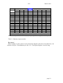
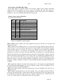
1
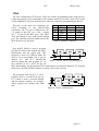
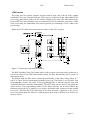
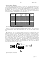
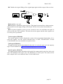
Check for most recent version:
http://www.nikhef.nl/pub/departments/et/L3/cosmics
NIK HEF
NATIONAL INSTITUTE FOR NUCLEAR AND HIGH ENERGY PHYSICS
ETR 99-02
version: March 1999
CPC
(Cosmics Personality Card)
for the L3+Cosmics experiment.
The CPC replaces the MPC in L3, which is the interface of
the muon chambers signals to the muon trigger. The CPC
splits the signals from the discriminators in the muon
system in L3. The old functionality of the MPC is copied
into new devices and interfaces to the existing trigger
system. Majority logic is added for a new trigger system for
L3+Cosmics and TDCs measure the relative timing of
muons. A stand alone read-out system in VME is used to
read the data independent from the existing L3 data
acquisition system.
This paper describes CPC version 3.
H.L. Groenstege
T.A.M. Wijnen
P.A.M. Rewiersma
J. Stolte
email: [email protected]
NIKHEF, DEPARTMENT OF
ELECTRONIC TECHNOLOGY
P.O.box 41882, NL 1009 DB AMSTERDAM
CPC
March 1999
Contents
INTRODUCTION ..................................................................................................................................... 4
ABOUT V3, MODIFIED V2 ......................................................................................................................... 4
MPC FUNCTIONALITY .......................................................................................................................... 6
CPC ............................................................................................................................................................ 7
SIGNAL SPLIT ........................................................................................................................................... 7
MAJORITY LOGIC ..................................................................................................................................... 7
READ OUT CONTROL LOGIC ....................................................................................................................... 8
CARD IDENTIFICATION.............................................................................................................................. 9
JTAG.........................................................................................................................................................10
JTAG CHAINS .........................................................................................................................................11
MASK AND TEST PATTERN ........................................................................................................................12
MAJORITY LOGIC ....................................................................................................................................14
SCINTILLATOR CPC ................................................................................................................................19
READ OUT CONTROL LOGIC ......................................................................................................................23
TDC PROGRAMMING ...............................................................................................................................28
14.1. JTAG instructions .................................................................................................................... 29
14.2. Boundary scan register. ........................................................................................................... 29
14.3. ID code.................................................................................................................................... 30
14.4. Setup registers ......................................................................................................................... 30
14.5. Control registers...................................................................................................................... 32
14.6. Status registers ........................................................................................................................ 32
14.7. Internal test registers............................................................................................................... 32
Figures
Figure 1: Signal flow from muon chambers .....................................................................................................4
Figure 2: CPC signal split, mask and test pulse ...............................................................................................7
Figure 3: MACH_PROG, programming port .................................................................................................10
Figure 4: JTAG2, emulated port ....................................................................................................................10
Figure 5: Chain orders and connector names .................................................................................................11
Figure 6: Majority output logic ......................................................................................................................17
Figure 8: JTAG, the TDC chain ....................................................................................................................28
Tables
Table 1: MPC registers....................................................................................................................................6
Table 2: MPC Control register.........................................................................................................................6
Table 3: MPC status register............................................................................................................................6
Table 4: MachPro connector ..........................................................................................................................10
Table 5: Mask/ test pattern, Instruction register .............................................................................................12
Table 6 : Testmode select ..............................................................................................................................12
Table 7: Majority logic, Instruction register ...................................................................................................14
Table 8: Majority logic, Set up.......................................................................................................................15
Table 9: Majority logic, Control ....................................................................................................................15
Table 10: Majority logic, input stretcher timing.............................................................................................17
Table 11: Majority output stretcher................................................................................................................18
Table 12: Scintillator, Instruction register......................................................................................................19
Table 13: Scintillator control register ............................................................................................................20
Table 14: Scintillator, stretch and delay.........................................................................................................22
Table 15: Scintillator, test point selector ........................................................................................................22
Table 16: Read Out Control, JTAG register selection.....................................................................................23
Table 17: Read Out Control: Control register ................................................................................................24
Table 18: Read Out Control: Setup register....................................................................................................25
Table 19: Read Out Control, Diagnostics register ..........................................................................................25
page 2
CPC
March 1999
Table 20: Read Out Control, Mode register....................................................................................................26
page 3
CPC
March 1999
Introduction
For the L3+Cosmics experiment the existing L3 muon chambers are used. The signals from the L3
discriminators are used to generate a trigger and to measure their relative timing. A convenient place
was found at the back of the existing muon TDC crates. There the MPCs (Muon Personality Cards)
connect the FastBus TDCs to the first and second level muon trigger. The signals on the auxiliary
connector are a copy of the discriminator signals that come in at the front panel of the TDC cards,
converted to TTL signals.
The MPCs are replaced by CPCs (Cosmic Personality Cards). On these cards the old (MPC)
functionality has been redesigned to occupy less space and consume less power. The added functions
are the majority logic needed for the L3+Cosmics trigger and a TDC system for time measurements
independently from the existing L3 system.
First a prototype (CPC0) was installed to demonstrate that the wire signals can be split to provide
the L3+Cosmics system with timing signals from the muon chambers, without disturbing or altering
the L3 muon trigger interface. These are now replaced by the final CPC.
Figure 1: Signal flow from muon chambers
About V3, modified V2
On version 3 (or modified version 2) the quality of the 40 MHz clock, driving the TDCs, is further
improved. The buffer that used to be located on a small modification card, mounted on the CPC_V2,
is replaced by a RoboClock (Cypess CY7B991). On the modified version 2 this is again a small
modification board. On version 3, it is integrated on the CPC itself.
Via a register in the majority logic (IC8) it can be checked whether the 40 MHz clock is running (see
Table 9). There is a difference here between the modified version 2 and version 3. In version 2 the
incoming clock from the front end link is monitored. In version 3 the clock from the RoboClock is
monitored. It is possible that the RoboClock still runs at its minimum frequency when the Front End
link is absent. This can only be checked by observing the lock error of the TDC or checking the
communication via the . front end link. If the CPC powers up without the input clock, the RoboClock
is quiet. When the clock is removed during running, its frequency drops to the minimum lock
frequency, which is somewhere between 10 and 20 MHz (guaranteed minimum frequency is 20 MHz).
page 4
CPC
March 1999
New test pulse functions have been implemented. This is in V3, as well in the modified V2. The
external testpulse, running on the JTAG cable, is now also available on the Read Out Controller
(IC7). And there is a connection, running from the ROC (Read Out Controller) to the Control-Mach
(IC3). This makes it possible to generate test pulses to the TDCs and majority inputs from the ROC.
From the external testpulse, the ROC can generate a trigger to the TDCs with a fixed delay in respect
of the TDC’s input pulses. The feature is added for testing purposes.
This test pulse must be enabled in the Control-Mach (see Table 5, control register). Though the
definition of the control register has changed, it is compatible with older routines, choosing between
the previously existing test pulse sources.
Modified V2 cards can easily be recognized by the copy of the serial number on the back side of the
RJ45 connector and the yellow connect LED, which used to be red. The serial numbers of V2 range
from x011 until x04c and the serial numbers for V3 start at x051.
page 5
CPC
March 1999
MPC functionality
The MPC is described in the paper “The L3 muon trigger interface”[1]. Since the functionality is
extended in the case of the CPC, it is described here briefly.
The MPC functions can be reached via the LeCroy FastBus TDC. Nine secondary addresses are
used to reach the data registers and status/ control address. For the CPC a new address is
implemented (C,3). Reading this location will return the card’s fixed address used in the addressable
JTAG chain (10 bits). This is the same as the card’s serial number. The identification register can be
used to store a 6 bit position identification via FastBus into the CPC. This will be further described in
the JTAG description.
Address
C,2
C,3
C,8...C,B
data registers
Read
Status
Card address
MPC registers
C,C...C,F
ORed inputs MPC
Write
Control
Identification
Add pattern to
MPC registers
Replace pattern
MPC registers
(C,2 is shorthand for address C0000002)
Table 1: MPC registers
A flip-flop on the MPC determines whether the card is controlled by the PCC (Personality Card
Controller) or from FastBus through the LeCroy TDC. The PCC overrides operations from FastBus.
When the PCC is master, the data registers cannot be accessed and an SS6 response is returned. The
48 bit data register is split in 4 parts of 12 bits, due to limitations on the auxiliary FastBus connector.
data
4
5
8
9
C
D
control (write C,2)
Enable collect
Disable collect
Set all registers
Reset all registers
TDC becomes master
let PCC be master
Bit
0
1
2
3
Status (read C,2)
PCC is reading the MPC
PCC is master of MPC
Collect enabled
Power failure on daisy chain circuit
Table 3: MPC status register
Table 2: MPC Control register
The enable/ disable collect commands set and reset a flip flop on the MPC. When this flip
flop is set, the 48 registers collect and store pulses from the inputs in the same way as the
registers are used by the PCC to collect wire signals. When the PCC becomes master, the flip
flop is reset automatically. Only when the TDC is master of the MPC, the data registers can
be accessed and the collect flip flop can be controlled. The TDC cannot become master of
the MPC when the PCC accesses the MPC at that moment.
1
The muon trigger interface for L3: MPC, PAC, PCC-P, PCC-Z, PCS and PCT, september 1989, H. Groenstege NIKHEF-ET.
page 6
CPC
March 1999
CPC
Signal Split
The signal split to the added functionality (majority logic and new TDCs2) is implemented
in the same devices that contain the MPC functionality. This strongly reduces the pin count
on the board. The old functionality has not been changed. The MACH 466 devices also
contain two sets of registers. One set of 96 bits is used to disable noisy channels (only for the
new functionality) . The other set of 96 bits is used to inject test patterns upon reception of a
test pulse.
Figure 2: CPC signal split, mask and test pulse
The two set of registers are configured to behave as a JTAG port, which is controlled by a
MACH 231 device. The bits are shifted with LSB (Least Significant Bit) first. Upon powerup, the registers are initialized automatically. All wire signals are enabled to the output and
the test pattern is reset. However, this cannot be guaranteed, since it requires the power
supply to rise monotonously. A power failure can be detected by checking a bit in the
Majority Logic, see page 15 (Majority logic, Control).
Majority logic
IC 8 contains the majority logic. It can run in two modes:
• The 96 inputs are compared with a single threshold.
• The 96 inputs are divided in an upper and a lower half (48 inputs each).
An input signal, longer then app. 15 ns, is recorded. All signals are stretched to app. 1.2 µs.
Every 200 ns the total number of hits is determined. This number is compared to the
programmable threshold and may thus generate a hit. This hit signal belongs to one of the
2
A 32 channel general purpose Time to Digital Converter, J. Christiansen CERN/ECP-MIC.
page 7
CPC
March 1999
three muon chamber layers; MI, MM or MO. A register setting determines which output has
to be activated. This output is a differential implementation of an open collector output. In
this way all CPCs in a crate can pull this line. This line then runs to the CTT (Cosmic Trigger
and Timing) module, where the Cosmic trigger is generated.
In every P-crate there is one location where signals from two different muon chamber layers
are connected to one FastBus TDC. In that case the majority logic works in the splitted
mode, with two times 48 channels. Two output signals are generated in the same way as
described above and can be routed (software controlled) to the MI, MM and MO outputs.
The majority logic chip (IC 8) receives the 40 MHz clock from the read out chip (IC 7).
This clock is divided internally to create the clock for the pulse stretchers and other pipe line
registers. This divider can be programmed to divide from 7 to 10.5 in eight steps. The setting
is done via JTAG. The pipe line clock periods thus vary from 175 to 263 ns, in 12.5 ns steps.
The pulse stretchers are active for seven of these cycles. So the one shots run for 1050 to
1575 ns, plus one clock period. The input signal is first stored in a register. On the next clock
cycle the one shot starts. This covers the maximum drift time plus one clock cycle for the
synchronization uncertainty. Also one clock cycle overlap is needed to determine the total of
active one shots. The drift time range is then 1050 to 1575 ns. For information how to set the
stretchers see page 14. The reset signal from the FELink can be used to synchronize the
clock dividers on the different CPCs.
For the scintillators the chip that normally contains the majority logic (IC 8) has an other
contents. It logically ORs every eight inputs, which results in 12 signals. These signals can be
used by three outputs to form larger ORs. These three outputs are first stretched and then
delayed. The stretcher is a retriggerable one-shot that is fired by the rising edge of the OR
signal. The delay is made by means of a shift register. For the settings see Table 14:
Scintillator, stretch and delay.
Read out control logic
The CPC Read Out Controller (ROC) in IC7 receives the clock (40 MHz) and control
signal (Reset/Trigger) from the NIMROD. The control signal encodes the Reset and Trigger
signals using a 3 bit pulse width scheme. Holding the control line high for one clock cycle,
followed by a low level for at least two clock cycles encodes the Trigger signal. Holding the
control line at high level for three consecutive cycles encodes the Reset signal.
The Reset and Trigger signals are distributed to the TDC chips and the Majority logic chip.
The Reset signal clears all internal counters and the data memory in the TDC chips. The
Trigger signal is used by the ROC to initiate the read out of the TDC chips. The data from
the TDC's is read out using a token ring scheme and the data is formatted by adding some
identification bits, serialized and sent to the NIMROD via the Front End Link. Data is
transferred via two pairs of Low Voltage Differential Signal (LVDS) drivers using the DataStrobe (DS) protocol. The bit rate is 40 Mbit/s and each data word is composed of a start
bit, 32 data bits, a parity bit and one stop bit. This results in a maximum data rate of
approximately 1 Mword/s.
Provisions have been made to be able to read out the Majority Logic as another node in the
token ring. This would allow the Majority Logic to send one word of information into the
data stream after a Trigger, whenever that becomes useful.
page 8
CPC
March 1999
Card identification
The card address (10 bits) is defined when it is tested after production. This is fixed. The
address is the same as its serial number written on the white space. The address is used by the
addressable JTAG controller to uniquely address a single card. When two cards in the
FastBus crate are swapped, this cannot be detected via the addressable JTAG branch. Two
provisions are implemented to deal with the problem:
• Using a geographical read cycle in FastBus, the card’s serial number can be read.
This serial number is used as an address in addressable JTAG operations. See the MPC
register description on page 6 (Table 1: MPC registers).
• Using a geographical write cycle in FastBus, an identifier can be written into C,3.
It is useful to write the card location inside the FastBus crate into this register. The stored
value can be read back via the addressable JTAG chain. See the FastBus control register
description on page 6 and the JTAG register description on page 12 (Table 5: Mask/ test
pattern, Instruction register).
Both methods require access to the L3 FastBus TDCs.
page 9
CPC
March 1999
JTAG
The CPC contains three JTAG ports. These are used for programming some of the devices,
testing the printed circuit board and for the settings needed at run time. Some JTAG ports
are the standard JTAG ports of the devices, others are created by programming the devices.
The pins on the dual row connectors are
wired according to the MACH-PRO
convention. The Vcc pin is connected to the
5 V supply of the CPC, via a 100 Ω resistor
(4.7 Ω in case of the BST port). The TRST
(Test bus Reset) is only used on the settings
port. The optional program enable pins on the
MACH devices are not used.
Pin
1
2
3
4
5
Signal
TCK
NC
TMS
GND
TDI
Pin
6
7
8
9
10
signal
Vcc
TDO
GND
TRST
NC
Table 4: MachPro connector
Port MACH_PROG is used to program
the MACH devices that emulate the MPC
functionality and the signal split. This
program is stored in EEProm inside the
devices. It is non-volatile, but it can be
altered. IC 1 and IC 2 (MACH 466
Figure 3: MACH_PROG, programming port
devices) contain the same program. IC 3 is
the controller of ICs 1 and 2 for the old
MPC functionality, for the emulated JTAG chain and for several other functions. To program
the devices, the MACH-PRO software (version 1.40f or later) is used.
The programs stored in IC1, 2 and 3
together create a second JTAG port on
IC3, which is used to load the disable
and test pattern registers, for example.
These registers are shifted with LSB
first.
Figure 4: JTAG2, emulated port
page 10
CPC
March 1999
JTAG chains
The mask and test pattern registers and the majority logic and read-out chips contain
emulated JTAG ports. Together with the TDCs they are connected to the addressable JTAG
port (Ajtag) that will be used to do the various settings on the card. The addressable JTAG
ports of all CPCs in one FastBus crate are connected to a JTAG controller, located in a VME
crate. For testing, the addressable part can be bypassed, by connecting a JTAG cable to the
port Settings.
Below the JTAG chain order and connector names on the CPC are given.
Figure 5: Chain orders and connector names
The BST (Boundary Scan Test) chain can be used to test the card electrically. In this case a
test set-up exists for the MPC functionality. Nearly all other functionality can be tested via
the Settings chain.
The EProm holds the files used to define the functionality of the Altera 10k20 chips, IC 7
and IC 8. These files are automatically loaded at power-up. The EProm is a OTP (One Time
Programmable) version. The order of the programming files is first the majority logic and
second the Read out controller functionality. The BST chain can be used to reprogram the
Altera devices. The programming routine of the Altera software can be used without the
hardware protection key. It requires a byte blaster download cable, connected to the parallel
port of PC. Because the JTAG chain runs in the other direction, compared to the passive
serial load chain (from the EProm), a valid program must reside in EProm to be able to use
the byte blaster.
page 11
CPC
March 1999
Mask and test pattern
The combined functionality of ICs 1, 2 and 3, besides creating the MPC functionality, is to
split the incoming signals to the TDCs and majority logic. They contain mask and test
registers. These are loaded via JTAG.
IR
0000
0001
0010
0011
Others
Instruction
Test pattern
Mask register
Control register
FastBus ID register
Bypass
Bits
96
96
4
6
1
R/W
R/W
R/W
R/W
R
R
Default
0…0
0…0
0000
00 0000
0
Table 5: Mask/ test pattern, Instruction register
Test pattern (IR=0000)
After loading the test pattern, test pulses can be generated in the Pause_DR state or the
Run-Test/Idle state of the TAP controller. Efficient tests (a walking bit, for example) can be
performed, by turning from Pause_DR back to Shift_Dr, instead of loading a complete new
96 bit pattern. This is possible, since the test pattern register does not have a shadow
register. One does not have to pass trough the Update_DR state to activate the pattern.
Usually the Run Test/Idle state is used to generate test pulses. For both states TMS is kept
zero to remain in the state. If the state is just passed, to go to another state (respectively
Exit2_DR and Select_DR_Scan), no test pulses are isued. The source and the length of the
pulses are determined by the contents of the control register.
Mask pattern (IR=0001)
Via this register noisy or unused channels can be disabled. Loading a one means disable this
channel for the TDCs and the majority logic.
Control register (IR=0010)
The control register contains four bits.
Bit 2…0
Test pulse
000
No test pulse
X01
Test pulse from TCK
X10
Test pulse from EXT (JTAG)
X11
Test pulse from ROC
100
Test pulse from instruction
Note
*1
*2
*2
*2
*3
Table 6 : Testmode select
*1: Power up state.
*2: The TAP controller must be in state Run-Test/Idle for test pulse generation.
*3: Writing X100 in the control register will generate a test pulse in the TAP controller
state Update_DR. Bit 2 is automatically reset in the next state of the TAP controller.
Bit 3: Disable test pulse cut. When set, the on board test pulses, initiated by one of the test
pulse sources, have the same length as the input pulses. At power up, the bit is reset. In that
case the test pulse width is limited to app. 125 ns.
page 12
CPC
March 1999
FastBus ID (IR=0011)
The FastBus ID register is a 6 bit read only register. It is used to verify the geographical
location of the CPC, see page 9 for the description.
IR=’others’
When loading an other pattern then those described here, the function is Bypass. This is
mandatory for IR=1111. The Bypass Register is one bit long.
page 13
CPC
March 1999
Majority logic
IC 8 contains the majority logic. It is set up via JTAG. It can run in two modes:
• The 96 inputs are compared with a single threshold.
• The 96 inputs are divided in an upper and a lower half (48 inputs each). Each half has
its own threshold register.
The instruction register is four bits long.
IR
Register
R/W
PU
0000
Threshold 0
R/W
0111 1111
0001
Threshold 1
R/W
0011 1111
0010
Set_up
R/W
0000 1111
0011
Control/ Status
R/W
0000 1X00
0100
Version
R
1000 0010
0101
Stretcher
R/W
0000 0011
Others Bypass
R
0
PU describes the power up situation. This can also be
forced by the reset bit in the control register.
Table 7: Majority logic, Instruction register
All registers are 8 bits long, except for the bypass register, which is one bit long.
Threshold register 0 (IR=0000)
Threshold register 0 contains the threshold (7 bits) for the lower half of the inputs or the
full 96 inputs. It is a read/ write register. During a write, bit 7 is ignored. When read back,
bit 7 is 0.
Threshold register 1 (IR=0001)
Threshold register 1 contains the threshold (6 bits) for the upper half of the inputs. It is a
read/ write register. During a write, bits 6 and 7 are ignored. When read back, bits 6 and 7
are 0.
page 14
CPC
March 1999
Set up register (IR=0010)
The set up register determines which outputs are driven when the total number of hits
exceeds the threshold. Bit 4 determines whether there are one or two outputs. At power up
the bit is reset. In that case there is one output. Bits 1 and 0 determine lower half (or total)
output selection. Bits 3 and 2 determine the upper half output selection. When the bit pairs
are 11, no output is selected.
Bits
PU
1:0
11
3:2
11
4
0
7:5
000
Value
00
01
10
11
00
01
10
11
0
1
Result
Hit0 to MI
Hit0 to MM
Hit0 to MO
No output
Hit1 to MI
Hit1 to MM
Hit1 to MO
No output
96 inputs
2*48 inputs
Comment
Hit0 is the result
from the total or
the lower half.
Hit1 is the result
from the upper half.
See also page 7.
Not used
PU describes the power up situation. This can also be forced by the
reset bit in the control register.
Table 8: Majority logic, Set up
The settings can be read back. Bits 7, 6 and 5 are zero. When the bit 4 is one and for both
halves the same output is selected, the two hit results are logically ORed.
Control/ Status register (IR=0011)
Bit
PU
Description
0
0
Hit 0 Register
1
0
Hit 1 Register
2
X
Clock running
3
1
Power up reset monitor
4
0
(Differential mode)
5
0
Enable drivers
6
1
Enable synchronization
7
0
Simulate power up
PU: Power Up situation
Table 9: Majority logic, Control
The hit 0 register (bit 0) in the control/ status register monitors whether the output of
lower half (or the total number of channels) of the majority logic has seen a hit. A hit means
that the number of active channels within the maximum drift time period has exceeded the
programmed threshold. The bit is reset when read (destructive read). Bit 1 does the same for
the upper half.
page 15
CPC
March 1999
Bit 2 monitors the 40 MHz clock. It is reset when the TAP controller passes the Runtest/Idle state. It is set by clocking a one by means of the 40 MHz clock, during the time the
TAP controller moves to Capture_DR. There is a difference here between the modified
version 2 and version 3. In version 2 the incoming clock from the Front End link is
monitored. In version 3 the clock from the RoboClock is monitored. It is possible that the
RoboClock still runs at its minimum frequency when the Front End link is absent. This can
only be checked by observing the lock error of the TDC or checking the communication via
the . front end link. If the CPC powers up without the input clock, the RoboClock is quiet.
When the clock is removed during running, its frequency drops to the minimum lock
frequency, which is somewhere between 10 and 20 MHz (guaranteed minimum frequency is
20 MHz).
Bit 3 registers a (hardware) power up reset. This signal is generated by a voltage monitor
chip connected to the supply voltage of the board. The bit is reset when read (destructive
read)
Bit 4 is not used.
Bit 5 is the output enable of the three majority output drivers.
Bit 6 enables synchronization of the one-shots in the majority logic. The reset signal from
the FELink is passed to the majority logic, via the read out chip. The front edge of the reset
signal is used to synchronize the pipe line clock. If the reset signal is longer then two clock
periods (of 25 ns), the majority output drivers are disabled until the reset drops again.
Register bit 7 is used to simulate a power up reset. It must be set to one and than reset
again. It does not affect the TAP controller. The other bits in the register and other registers
are set to the power up situation.
Version register (IR=0100)
The Version register is used to identify the version of the programmed functionality. It is a
read only register. For the version described here it reads 1000 0010.
page 16
CPC
March 1999
Stretcher register (IR=0101)
The Stretcher register determines the speed of the one shots. Since the input pulses have to
be synchronized with the digital one_shot’s clock, the total length must be the drift time plus
one clock cycle. The clock for the one_shots is derived from the 40 MHz clock, coming from
the NIMROD. This clock is divided to obtain the pipe line clock. Six clock cycles from the
divider are used for the drift time by the one shot and one more for the synchronization
uncertainty. For the L3 muon chambers the drift time is app. 1.2 µs.
Bit 2:0
÷N
000
7
001
7.5
010
8
011 *
8.5
100
9
101
9.5
110
10
111
10.5
*: Power up setting.
Pipe
Clock
[ns]
175
188
200
213
225
238
250
263
Drift
Time
[ns]
1050
1125
1200
1275
1350
1425
1500
1575
Stretch
Time
[ns]
1225
1313
1400
1488
1575
1663
1750
1838
Table 10: Majority logic, input stretcher timing
The halves in the table are created by alternating dividing by N and N+1. The stretch time is
the maximum drift time plus the input synchronization time. This is the time that the one-shot
runs.
Bit 3 disables the time over threshold output. Comparators in the majority logic check
whether the amount over one-shots running is more then specified in the threshold register.
This is done every pipe-line clock. Thus the output of the comparator is time over threshold.
The rising edge of this signal starts a one-shot. The one-shot then runs for a period specified
in bits 7 to 4. When a new rising edge of the time over threshold is detected while the oneshot is already running, the one-shot is restarted. So it is a retriggerable one-shot. Restarting
does not introduce gaps in the output signal. The output of this one-shot is logically ORred
with the time over threshold signal and forms the majority output towards the CTT. Setting
bit 3 disables the ORing of the time over threshold. In that case only the one-shot output is
seen at the output. At power up, bit 3 is reset.
Figure 6: Majority output logic
page 17
CPC
ns
bits 2:0 (Pipeline clock, see Table 10)
Bits
000
001
010
011*
7:4
175
188
200
213
175
188
200
213
0000
175
188
200
213
0001
350
376
400
426
0010
525
564
600
639
0011
700
752
800
852
0100
875
940
1000
1065
0101
1050
1128
1200
1278
0110
1225
1316
1400
1491*
0111*
1400
1504
1600
1704
1000
1575
1692
1800
1917
1001
1750
1880
2000
2130
1010
1925
2068
2200
2343
1011
2100
2256
2400
2556
1100
2275
2444
2600
2769
1101
2450
2632
2800
2982
1110
2625
2820
3000
3195
1111
*: Power up setting
*: Power up setting
March 1999
100
225
225
225
450
675
900
1125
1350
1575
1800
2025
2250
2475
2700
2925
3150
3375
101
238
238
238
476
714
952
1190
1428
1666
1904
2142
2380
2618
2856
3094
3332
3570
110
250
250
250
500
750
1000
1250
1500
1750
2000
2250
2500
2750
3000
3250
3500
3750
111
263
263
263
526
789
1052
1315
1578
1841
2104
2367
2630
2893
3156
3419
3682
3945
The minimum pulse width of the majority output signals is one pipeline clock cycle.
Table 11: Majority output stretcher
IR=’others’
When loading an other pattern in the Instruction Register then those described here, the
function is Bypass. This mandatory for IR=1111. The Bypass Register is one bit long.
page 18
CPC
March 1999
Scintillator CPC
The programming of IC 8 is different for the scintillator CPC, used in the auxiliary box.
The chip that normally contains the majority logic (IC 8) has an other contents. It logically
ORs every eight inputs, which results in 12 signals. These signals can be used by three
outputs to form larger ORs. These three outputs are first stretched and then delayed. The
stretcher is a retriggerable one-shot that is fired by the rising edge of the OR signal. The
delay is made by means of a shift register.
Also IC 1, 2 and 3 behave different. The FastBus interface is removed and the FB_ID will
always return 00 0000 via Jtag. The 96 inputs are positive inputs for this version, instead of
active low as needed for the interface to the LeCroy TDC. The mask and test pattern act the
same as in the normal CPC.
Figure 7: IC 8 for scintillator CPC
IR
Register
R/W
PU
0000
Select pattern 1
R/W
0000 0000 0000
0001
Select pattern 2
R/W
0000 0000 0000
0010
Select pattern 3
R/W
0000 0000 0000
0011
Control/ Status
R/W
0100 0111 X000
0100
Version register
R
1100 0000 0010
0101
Clock divider
R/W
0000 0000 0011
0110
Stretch register
R/W
1001 1001 1001
0111
Delay register
R/W
0110 0110 0110
1000
Test point register
R/W
0000 0111 1111
PU describes the power up situation. This can also be forced
by the reset bit in the control register.
Table 12: Scintillator, Instruction register
page 19
CPC
March 1999
Select pattern (IR=0000, 0001, 0010)
Every eight inputs are logically ORred. For the three outputs, these patterns determine
which of these twelve groups are used to create the complete OR. The select pattern is
numbered 1 to 3, according to the octant numbers. On the board and in the schematics,
outputs 0, 1 and 2 are called MI, MM and MO respectively.
Control/ status register (IR=0011)
The control/ status register
Bit
PU
Description
0
0
Hit register 1
1
0
Hit register 2
2
0
Hit register 3
3
X
Clock running
4
1
Differential mode
5
1
Enable output drivers
6
1
Enable synchronization
7
0
NoOR
8,9
00
Not used
10
1
Power up reset monitor
11
0
Simulate power up
PU: Power Up situation
Table 13: Scintillator control register
Bit 0, 1 and 2 register whether one of the outputs has seen a hit. The bits are reset when read
(destructive read).
Bit 3 monitors the 40 MHz clock. It is reset when the TAP controller passes the Runtest/Idle state. It is set by clocking a one by means of the 40 MHz clock, during the time the
TAP controller moves to Capture_DR. There is a difference here between the modified
version 2 and version 3. In version 2 the incoming clock from the Front End link is
monitored. In version 3 the clock from the RoboClock is monitored. It is possible that the
RoboClock still runs at its minimum frequency when the Front End link is absent. This can
only be checked by observing the lock error of the TDC or checking the communication via
the . front end link. If the CPC powers up without the input clock, the RoboClock is quiet.
When the clock is removed during running, its frequency drops to the minimum lock
frequency, which is somewhere between 10 and 20 MHz (guaranteed minimum frequency is
20 MHz).
Bit 4 controls the mode of operation of the output drivers. The outputs are truly differential
or the differential implementation of an open collector output. For the scintillator CPC it
should be set (power up, default situation).
Bit 5 is the output enable of the three output drivers. For the scintillator CPC the bit is set
during power up.
Bit 6 enables synchronization of the clock divider. The reset signal from the FELink is
passed to the stretcher logic, via the read out chip. The front edge of the reset signal is used
to synchronize the pipe line clock. If the reset signal is longer then two clock periods (of
25 ns), the output drivers are disabled until the reset drops again.
page 20
CPC
March 1999
Bit 7 disables the logical ORing of the original input signal with the output of the one-shot.
Bits 8 and 9 are not used.
Bit 10 registers a (hardware) power up reset. This signal is generated by a voltage monitor
chip connected to the supply voltage of the board. The bit is reset when read (destructive
read).
Bit 11 is used to simulate a power up reset. It must be set to one and than reset again. It
does not affect the TAP controller. The other bits in the register and the other registers are
set to the power up situation.
Version register (IR=0100)
The version register is used to identify the version of the programmed functionality. It is a
read only register. For the version described here it reads 1100 0000 0010. Version
1100 0000 0001 does not contain the test point selector.
Clock speed (IR=0101)
The pipe line clock speed is determined by three bits. It works the same as for the majority
logic. For the definition see Table 10: Majority logic, input stretcher timing.
Stretch register (IR=0110)
The output stretch register determines the length of the output pulse in pipe line clock cycle
units. The minimum is one clock cycle. The maximum is 15 clock cycles. The values for the
three outputs can be set to different values. See the table below.
page 21
CPC
March 1999
Delay register (IR=0111)
The delay register determines the length of the output pulse in pipe line clock cycle units.
The minimum is one clock cycle. The maximum is 15 clock cycles. One more clock cycle is
used in the pipe line structure. The values for the three outputs can be set to different values.
Output
Bits
default
Stretch
Delay
Bit groups for stretch and delay registers
3
2
1
11:8
7:4
3:0
1001
1001
1001
0110
0110
0110
Table 14: Scintillator, stretch and delay
Use Table 11 to determine the values in ns.
Test point register (IR=1000)
The test point register selects one of the 96 inputs to be routed to pin 7 of connector Diag8
on the CPC.
Write
XXXX XSSS SSSS
Test point register
Read
0000 0SSS SSSS
Power up
0000 0111 1111
Table 15: Scintillator, test point selector
Valid range for input selection is 0 to 95. If a higher value is written (96…127), the output
is zero. Please note that the input is taken after the mask and test pattern section of the CPC.
Diagnostics connector
Diagnostics connector Diag 8 carries the following signals:
Pin
Name
Use
1
Vcc
+5 V
2
Clk_div
Divided clock used by IC 8
3
Dia8p9
In CPC V2 used to connect to IC 7
4, 5, 6
TPM4, 3, 2
Not used
7
TPM1
Test point output, see test point register
8
_PUR
Power up reset monitor of IC 8 only
9…12
TPM7, 8, 5, 6
Not used
13
_A_Hit
Stretched hit signal
14, 15, 16
MO_D, MM_D, MI_D
Logic one / active in scintillator CPC
17, 18, 19
MO_E, MM_E, MI_E
Majority outputs / logic one in scintillator CPC
20
Gnd
0V
page 22
CPC
March 1999
Read out control logic
The chip IC 7 contains the Read Out Control logic (ROC). It is set up via JTAG and the
clock, trigger and reset signals are handled to acquire and send out the TDC data via the
Front End Link.
Front End Link
The clock, trigger and reset signals are sent from the Cosmic Trigger and Timing unit to the
CPC cards via the Front End Link cable (standard FTP-type cable with RJ45 connectors)
using differential LVDS drivers and receivers. The clock is transmitted via one pair of wires,
the other signals are time-encoded over one other pair of wires. The encoder uses three
consecutive cycles of the 40 MHz clock and uniquely defines the four signals as follows:
t1
0
1
1
1
1
t2
0
0
1
0
1
t3
0
0
0
1
1
Description
no operation
Trigger
bunch count reset: resets only the TDCs
event count reset: reset the ROC and the TDCs
global reset: resets the ROC and the TDCs
Data format
The data format that the ROC generates is described in a separate document called “The L3 +
Cosmics Data Format” by T. Wijnen, B. Petersen and C. Timmermans.
JTAG
The JTAG instruction register is four bits long and it is used to select one of the internal
data registers.
IR
0000
0001
0010
0011
0100
0101
0110
0111
1111
Others
Register
User identity
Control
Setup
Version
Diagnostics
DAC
Mode
Rand
Bypass
Bypass
Mode
R/W
R/W
R/W
R
R
R/W
R/W
R/W
R
R
Default
1111 1111
1100 0000
0010 0000
1000 0110
0000 0000
1000 0000
0000 0000
0000 0000
0
0
Table 16: Read Out Control, JTAG register selection
page 23
CPC
March 1999
All data registers are 8 bits long, except for the Bypass Register, which is one bit long. The
default value is the contents of the data registers at power up.
User Identity Register (IR=0000)
The eight bits User Identity register is used to identify the card when read out via the front
end link (FELink). It can be filled with e.g. the crate number and card position.
In the current version (dated 12-Mar-1999) this information can not be read out via the
FELink!
Control Register (IR=0001)
The Control register is used to control the functions of the ROC. The contents of the
register may only be changed when the trigger system is disabled, because otherwise the
ROC functions could be altered or aborted while it is processing data. The individual bits
have the following meaning:
Bit
0
1
2
3
4
Function
CR0
CR1
EnTTrigger
EnMTrigger
EnETrigger
Default
0
0
0
0
0
5
EnART
0
6
7
Inhibit FE Link
Inhibit ROC
1
1
Description
Clock speed select for ROC test pulse
Clock speed select for ROC test pulse
Enable ROC test pulse trigger
Enable "internal" Majority Trigger signal
Enable external Trigger and Reset signal from
test connector
Enable the artificial Reset/Trigger signals
( these are generated via EnTTrigger,
EnETrigger and EnMTrigger )
Disable Reset/Trigger signals via FELink
Disable ROC (holds the Reset signal for the
ROC and TDCs
Table 17: Read Out Control: Control register
After power up the Control register is preset to "1100 0000" and it is thus holding the
Reset signal for the ROC chip and the three TDC chips is a steady active state.
page 24
CPC
March 1999
Setup Register (IR=0010)
The Setup register is used to setup the different modes and options in the ROC. The
contents of this register may be altered only when the trigger system is paused, because any
change causes the token ring read out scheme to be altered immediately. The individual bits
have the following meaning:
Bit
0
1
2
3
4
5
6
7
Function
EnTDC
Unused
Unused
EnMAJ *
Unused
EnEOG
EnFake
EnEcnt
Default
1
0
0
0
0
1
0
0
Description
Enable the read out of TDCs
Enable the read out of the Majority Logic
Enable the End Of Group word
Enable the fake TDC words
Enable the Event Count word
Table 18: Read Out Control: Setup register
The function bits marked with “*” are not implemented in this version of the ROC chip,
dated 12-Mar-1999.
Version Register (IR=0011)
The Version register is used to identify the version number of the programmed functionality
in this chip. It is used to determine which "firmware" is present on this CPC card. This
version (12-Mar-1999) of the ROC will identify itself with a value of "1000 0110". At power
up this value is loaded from the configuration PROM.
Diagnostics Register (IR=0100)
The Diagnostics register allows to user to check on various internal signals of the ROC chip
to verify that it is functioning properly. It may also provide a means to diagnose problems.
After power up all bits are zero but they may turn on at any time. In the current version of
the ROC, the individual bits have the following meaning:
Bit
Signal
Default
Description
0
Active
0
a TDC or an internal register is active (i.e. it
has the token and is sending data
1
DataReady
0
a TDC or an internal register has set the
Data Ready signal
2
TokenAway
0
the ROC has sent out the token to the TDCs
3
TdcAct
0
the OR of the TDC Active signals
4
TdcErr
0
the OR of the TDC Error signals
5
GetData
0
the ROC is asking for data from a TDC or
an internal register
6
SerBusy
0
the data serializer is busy sending a word via
the FELink (Data/Strobe output lines)
7
SendEvent
0
the ROC received a trigger and is sending
out data belonging to this event
Table 19: Read Out Control, Diagnostics register
page 25
CPC
March 1999
This register is primarily intended to be used by experts only. The register is read only and
does not require to be initialized via the JTAG port. The signals that are attached to the
individual bits, may vary between different versions of the ROC (see also diagnostics
connector).
DAC Register (IR=0101)
The DAC register drives the Digital-Analog-Converter chip on the Datimizer card (this is a
front-end board for a wire chamber). This register has no use on the CPC card, but it is kept
here for compatibility.
Bits
7…0
Function
DAC
Default
0000 0000
Description
Threshold value for discriminators
Mode Register (IR=0110)
The DAC register drives the Digital-Analog-Converter chip on the Datimizer card (this is a
front-end board for a wire chamber). This register has no use on the CPC card, but it is kept
here for compatibility.
Bit
0
1
2
3
4
5
6
7
Signal
ART0
ART1
ART2
TS3
TS4
TS5
Spare6
Spare7
Default
0
0
0
0
0
0
0
0
Description
Artificial Reset/Trigger selector
"
"
test output on connector roc_ts pin 3
test input on connector roc_ts pin 4
test input on connector roc_ts pin 5
Spare
Spare
Table 20: Read Out Control, Mode register
The encoding of the ART (artificial reset and trigger) bits is as follows:
ART2
0
0
0
0
1
1
ART1
0
0
1
1
0
1
Others
ART0
0
1
0
1
0
1
Description
no operation
Trigger
bunch count reset: resets only the TDCs
event count reset: reset ROC and the TDCs
global reset: resets ROC and the TDCs
emulate power up reset inside ROC
no operation
RAND Register (IR=0111)
The RAND register provides a way to set a seed for the internal 9 bit random number
generator. The generated number is used as a word count for the fake TDC word unit. When
the EnFake bit in the Setup register is set, a random number of fake TDC words is inserted
page 26
CPC
March 1999
into the data stream that is sent out via the FELink. The fake TDC word is formatted as
"33xxxxxx", where the lower 24 bits are filled with a rotating bit pattern.
Bits
7…0
Function
RAND
Default
0000 0000
Description
Seed for random number generator
Bit 7 and 6 of the seed are AND-ed with the generated random number to form the fake
word count for one event, in order to limit the maximum word count. So the maximum word
count will either be 63, 127, 191 or 255. Each trigger will get the next number from the
pseudo random number generator.
Bypass Register (IR=1111 or IR=’others’)
When loading a different pattern than those described above into the instruction register,
the function is Bypass. This is also mandatory for IR=1111. The bypass register is one bit
long and its data is always “0”.
Diagnostics connector
There is a diagnostics connector on the CPC card where one can monitor several signals of the
ROC chip.
pin
1
2
3
4
5
6
7
8
9
10
11
12
Signal
Vcc
ClkA
Trigger
GetDataIn
DataReady
CTrigger
CTokenOut
CTokenIn
ROReset
PowerUp
SEvent
Diag bit
7
13
SerBusy
6
14
GetData
5
15
16
17
18
TdcErr
TdcAct
TokenAway
DataReady
4
3
2
1
19
Active
0
20
Gnd
-
Description
Vcc (+ 5 Volt).
not connected
the clock signal of the ROC
the trigger signal of the ROC and TDCs
the internal GetData signal (for bog/eog)
the internal DataReady signal ( " )
the internal Trigger signal
the token signal sent out to the TDCs
the token signal coming from the TDCs
the internal ROC Reset signal
the internal PowerUp signal (active low)
the ROC received a trigger and is sending out
data belonging to this event
the data serializer is busy sending one word
via the FELink (Data/Strobe output lines)
the ROC is asking for data from a TDC or an
internal register
the OR of the TDC Error signals
the OR of the TDC Active signals
the ROC has sent out the token to the TDCs
a TDC or an internal register has set the Data
Ready signal
a TDC or an internal register is active (i.e. it
has the token and is preparing data for readout
Ground (0 Volt)
page 27
CPC
March 1999
TDC programming
The Ajtag or Settings JTAG port
connects to the TDC chips according the
order shown in Figure 8. See Figure 5 for
the location in the total chain. It is used to
load the settings of the TDC chips and
check their status. The TDC’s JTAG ports
are in accordance with the IEEE 1149.1
standard.
Figure 8: JTAG, the TDC chain
The text and tables below are copied from
3
Christiansen’s TDC description [ ] version
0.4, chapter 14. For the most recent information one should use the TDC’s manual.
JTAG Test and Programming Port.
A JTAG (Joint Test Action Group, IEEE 1149.1 standard [3,4] port is used to program the
programmable features in the TDC, and also to get access to test facilities built into the TDC.
The JTAG protocol is today an accepted standard for chip and module testing, and easy to
use debugging tools are available on PCs. Full boundary scan is supported to be capable of
performing extensive testing of TDC modules while located in the system. Testing the
functionality of the chip itself is also supported by the JTAG INTEST capability. In addition
special JTAG registers have been included in the data path of the chip to be capable of
performing effective testing of all the timing registers and embedded memory structures.
Programming of the device is separated into two scan path groups. The setup group
consists of setups which can not be changed while the system is actively running (trigger
window, looking back window, enable of trigger matching, etc.) and a control group which
can be changed during a run (enable and disable of noisy channels). To save silicon area for
the large shift registers for the programming data they are not made with two sets of JTAG
registers (shift register and update register). This has the inconvenience that if the
programming data are read via JTAG (only used during functional testing of devices) one of
the programming bits will be lost and the bit sequence will be shifted by one.
An additional scan path is available to read status information from the TDC while it is
running (error flags).
3
A 32 channel general purpose Time to Digital Converter, J. Christiansen CERN/ECP-MIC.
page 28
CPC
March 1999
14.1. JTAG instructions
The JTAG instruction register is 4 bits long and is in full accordance with the IEEE 1149.1
standard. The JTAG controller macro from ES2 does not support being read from JTAG.
When passing through the JTAG state CAPTURE-DR the instruction register gets set to
0001 Bin (IDCODE).
0000
0001
0010
0011
0100...0111
1000
1001
1010
1011
1100...1110
1111
EXTEST. Boundary scan for test of inter-chip connections on module.
IDCODE. Scan out of chip identification code.
SAMPLE. Sample of all chip pins via boundary scan registers.
INTEST.
Using boundary scan registers to test chip itself.
NOT IMPLEMENTED.
Setup.
Load of setup data.
Control.
Load of control information.
Status.
Read of status information.
Coretest
Access to internal test scan registers.
NOT IMPLEMENTED.
BYPASS.
14.2. Boundary scan register.
All signal pins of the TDC are passed through JTAG boundary scan registers. All JTAG test
modes related to the boundary scan registers are supported (EXTEST, INTEST, SAMPLE).
BSR#
0
1
6:2
22:7
28:23
29
30
31
32
33
49:34
50
51
52
53
54
87:55
88
Pin name
Enable data_ready
Enable bus
Vernier[4:0]
Coarse_out[15:0]
Channel[5:0]
Rising
Active
Event_end
Data_ready
Error
Coarse_in[15:0]
Chip_select
Next_event
Get_data
Trigger
Reset
Hit[32:0]
Clk
Description
Enable of data_ready driver (not a direct pin).
Enable of read-out bus drivers (not a direct pin).
Read-out vernier.
Read-out time coarse out.
Read-out channel.
Read-out rising edge.
TDC active in read-out.
Read-out event end.
Read-out data ready.
Programmable error status output.
Read-out time coarse in (parallel trigger in).
Read-out chip select.
Read-out next event.
Read-out get data.
Trigger in
Reset of buffers and counters.
Hits.
Clock.
page 29
CPC
March 1999
14.3. ID code
A 32 bit chip identification code can be shifted out when selecting the ID shift chain.
0
11: 1
27: 12
31: 28
ES2 code
TDC part code
Version code
Start bit = 1.
ES2 manufacturer code = 00001000111.
decimal 3500 = binary 0000110110101100
first version = 0000
14.4. Setup registers
The JTAG setup scan path is used to load programming data that can not be changed while
the TDC is actively running. For testing purposes it is possible to read the status of internal
counters via this scan path.
15:0
16
17
18
34:19
35
36
37
45:38
53:46
54
55
56
72:57
78:73
86:79
87
89:88
94:90
95
96
97
98
99
100
101
Yes/no trigger time tag offset[l5:0]. (read back of trigger time tag counter)
Enable parallel trigger. *1
Enable sync trigger. *1
Enable serial trigger. *1
Trigger matching window [15:0]. (read back of active trigger)
Enable read-out of start measurements.
Enable subtraction of trigger time tag.
Enable overlapping triggers.
Looking back window[7:0]
Looking ahead window [7:0]
Enable subtraction of start time measurement (channel 32)
Enable matching
Enable automatic reject
Reject offset[15:0]. (read back of reject counter)
Adjust_channel[5:0]
Adjust[7:0]
Enable_individual_adjust
Test mode:
00 = normal mode,
01 = Coarse, Vernier, channel, falling from internal test scan path,
10 = Vernier from internal test scan path,
11 = Toggle between internal test scan path and its inverted value.
DLL_current_level_b[4:0], charge pump current levels inverted.
For normal operation = 11110 bin (minimum current levels).
DLL reset
Detect falling edge start
Detect falling edge odd channels
Detect falling edge even channels
Detect both edges (all channels)
Enable empty start
Must be equal to setup bit 54
page 30
CPC
March 1999
102
Enable use of double synchronisers.
103
Enable double hit priority queue.
104
Enable start gating
120:105
Coarse count offset[15:0] (read back of coarse count)
121
Enable token read-out mode.
122
Not_locked error mask.
123
Hit_error error mask.
124
Event_buffer_overflow error mask.
125
Trigger_buffer_overflow error mask.
126
Serial_trigger_error error mask.
*1: Only one of the three trigger modes can be enabled.
14.4.1.Programming of channel adjustment constants.
The programming of the channel adjustment constants are a bit more complicated than the
other programmable parameters loaded via the setup scan path. The required 32 eight bit
channel adjustment constants are not directly accessible as individual fields of the setup scan
path. The 32 channel specific constants are stored in a memory written into via the setup scan
path. The adjustment constant for the start channel (or the common adjustment constant) is
taken as the last adjustment constant shifted into the setup scan chain (not contained in
channel adjustment memory). This approach saves significant silicon area but requires the
adjustment constants to be loaded one by one using the serial JTAG protocol. In case only a
common adjustment is required the channel adjustment memory can be left non initialized.
Loading of one of the channel adjustment constants into the channel adjustment memory is
performed as follows. The channel identifier Adjust_channel[5:0] and its corresponding
adjustment constant Adjust[7:0] must be loaded into the setup scan path. When the setup
data have been loaded, and the JTAG controller gives a update signal (by passing through the
JTAG state: UPDATE) to the JTAG registers, the adjustment constant will be written into
the memory position pointed to by the channel identifier. The other bit fields of the setup
data can be left undefined during the loading of the channel specific adjustment constants.
The loading of the common (or start) adjustment constant must be performed as the last
loading of the setup scan chain. The channel identifier must in this case be set to
Adjust_channel[5:0]=10 0000 bin to signal that this value shall not be written into the
adjustment memory, but must remain in the normal JTAG scan register. In addition all the
other programming parameters in the setup chain must have all their parameters set as
required for the application.
14.4.2. Performing a reset of the DLL.
The Delay Locked Loop is not initialized when the reset pin of the TDC chip is asserted.
The lock tracing of the DLL is a rather slow process and is only required to be performed
once after power has been applied. The normal reset pin of the TDC can be used at regular
intervals to initialize all counters and buffers in the TDC without having to wait for the DLL
to acquire lock.
A reset of the DLL must be performed via the JTAG setup scan path after power up. First a
load of the setup registers must be performed with the DLL_reset signal assigned to a logical
one and the required charge pump current levels set to their correct value. For this to
perform a real reset of the DLL it is required that the JTAG controller issues an update by
being passed through the update state of the JTAG port controller [3,4]. To enable the DLL
to start lock tracing from its reset state the DLL_reset signal must be released again in the
page 31
CPC
March 1999
same manner. Now the DLL will start lock tracing and when lock has been obtained the
not_locked status bit will be cleared.
14.5. Control registers
The JTAG control scan path is used to enable/disable channels which can be done while the
TDC is actively running.
32:0 Channel enable [32:0]
14.6. Status registers
The JTAG status scan path is used to get access to the error status of the TDC while it is
running (or after a run).
0 Not_locked.
1 Hit_error.
2 Event_buffer_overflow.
3 Trigger_buffer_overflow.
4 Serial_trigger_error.
14.7. Internal test registers
The JTAG internal test scan path is used to perform extended testing of the TDC chip. The
internal scan path gives direct access to the interface between the hit registers and first level
buffer logic. It is used in connection with the test mode select bits in the setup scan path.
31:0
Vernier in non encoded form [31:0].
47:32 Coarse[15:0]
53:48 Channel[5:0]
54
Falling edge
55
Select difference (read only)
56
Select start (read only)
57
Store start (read only)
58
Store event (read only)
page 32