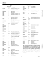
1
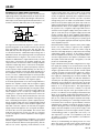
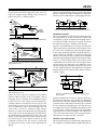
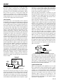
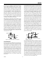
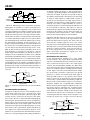
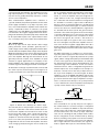
a
AN-202
APPLICATION NOTE
One Technology Way • P.O. Box 9106 • Norwood, MA 02062-9106 • 781/329-4700 • World Wide Web Site: http://www.analog.com
An IC Amplifier User’s Guide to Decoupling, Grounding,
and Making Things Go Right for a Change
By Paul Brokaw
“There once as a breathy baboon
Who always breathed down a bassoon,
For he said "It appears
that in billions of years
I shall certainly hit on a tune”
(Sir Arthur Eddington)
This quotation seemed a proper note with which to begin
on a subject that has made monkeys of most of us at one
time or another. The struggle to find a suitable configuration for system power, ground, and signal returns too
frequently degenerates into a frustrating glitch hunt.
While a strictly experimental approach can be used to
solve simple problems, a little forethought can often
prevent serious problems and provide a plan of attack if
some judicious tinkering is later required.
The subject is so fragmented that a completely general
treatment is too difficult for me to tackle. Therefore, I’d
like to state one general principle and then look a bit more
narrowly at the subject of decoupling and grounding as
it relates to integrated circuit amplifiers.
. . . Principle: Think—where the currents will flow.
I suppose this seems pretty obvious, but all of us tend to
think of the currents we’re interested in as flowing “out”
of some place and “through” some other place but often
neglect to worry how the current will find its way back to
its source. One tends to act as if all “ground” or “supply
voltage” points are equivalent and neglect (for as long
as possible) the fact that they are parts of a network of
conductors through which currents flow and develop
finite voltages.
In order to do some advance planning it is important to
consider where the currents originate and to where they
will return and to determine the effects of the resulting
voltage drops. This, in turn, requires some minimum
amount of understanding of what goes on inside the circuits being decoupled and grounded. This information
may be lacking or difficult to interpret when integrated
circuits are part of the design.
Operational amplifiers are one of the most widely used
linear lCs, and fortunately most of them fall into a few
REV. B
classes, so far as the problems of power and grounding
are concerned. Although the configuration of a system
may pose formidable problems of decoupling and signal
returns, some basic methods to handle many of these
problems can be developed from a look at op amps.
OP AMPS HAVE FOUR TERMINALS
A casual look through almost any operational amplifier
text might leave the reader with the impression that an
ideal op amp has three terminals: a pair of differential
inputs and an output as shown in Figure 1. A quick review
of fundamentals, however, shows that this cannot be
the case. If the amplifier has an output voltage it must be
measured with respect to some point . . . a point to
which the amplifier has a reference. Since the ideal op
amp has infinite common-mode rejection, the inputs are
ruled out as that reference so that there must be a fourth
amplifier terminal. Another way of looking at it is that if
the amplifier is to supply output current to a load, that
current must get into the amplifier somewhere. Ideally,
no input current flows, so again the conclusion is that a
fourth terminal is required.
A
Figure 1. Conventional "Three Terminal" Op Amp
A common practice is to say, or indicate in a diagram,
that this fourth terminal is “ground.” Well, without getting into a discussion of what “ground” may be, we can
observe that most integrated circuit op amps (and a lot
of the modular ones as well) do not have a “ground”
terminal. With these circuits the fourth terminal is one or
both of the power supply terminals. There is a temptation here to lump together both supply voltages with the
ubiquitous ground. And, to the extent that the supply
lines really do present a low impedance at all frequencies
within the amplifier bandwidth, this is probably reasonable. When the impedance requirement is not satisfied,
however, the door is left open to a variety of problems
including noise, poor transient response, and oscillation.
AN-202
positive supply have only a minor effect on the signal
output. The difference between these sensitivities can
result in an apparent asymmetry in the amplifier transient
response. If the amplifier is driven to produce a positive
voltage swing across its rated load, it will draw a current
pulse from the positive supply. The pulse may result in a
supply voltage transient, but the positive supply rejection
will minimize the effect on the amplifier output signal. In
the opposite case, a negative output signal will extract a
current from the negative supply. If this pulse results in a
“glitch” on the bus, the poor negative supply rejection will
result in a similar “glitch” at the amplifier output. While a
positive pulse test may give the amplifier transient response,
a negative pulse test may actually give you a pretty good
look at your negative supply line transient response, instead
of the amplifier response!
DIFFERENTIAL-TO-SINGLE-ENDED CONVERSION
One fundamental requirement of a simple op amp is that an
applied signal that is fully differential at the input must be
converted to a single-ended output. Single-ended, that is,
with respect to the often neglected fourth terminal. To see
how this can lead to difficulties, take a look at Figure 2.
V+
–IN
+IN
OUTPUT
CURRENT
MIRROR
V–
Figure 2. Simplified “Real” Op Amp
The signal flow illustrated by Figure 2 is used in several
popular integrated circuit families. Details vary, but the
basic signal path is the same as the 101, 741, 748, 777,
4136, 503, 515, and other integrated circuit amplifiers. The
circuit first transforms a differential input voltage into a
differential current. This input stage function is represented
by PNP transistors in Figure 2. The current is then converted from differential to single-ended form by a current
mirror that is connected to the negative supply rail. The
output from the current mirror drives a voltage amplifier
and power output stage that is connected as an integrator.
The integrator controls the open-loop frequency response,
and its capacitor may be added externally, as in the 101, or
may be self-contained, as in the 741. Most descriptions of
this simplified model do not emphasize that the integrator has, of course, a differential input. It is biased positive
by a couple of base emitter voltages, but the noninverting
integrator input is referred to the negative supply.
Remember that the impulse response of the power supply
itself is not what is likely to appear at the amplifier.
Thirty or forty centimeters of wire can act like a high Q
inductor to add a high-frequency component to the normally
overdamped supply response. A decoupling capacitor
near the amplifier won’t always cure the problem either,
since the supply must be decoupled to somewhere. If the
decoupled current flows through a long path, it can still
produce an undesirable glitch.
Figure 3 illustrates three possible configurations for negative supply decoupling. In 3a, the dotted line shows the
negative signal current path through the decoupling and
along the ground line. If the load “ground” and decoupled
“ground” actually join at the power supply, the “glitch”
on the ground lines is similar to the “glitch” on the negative supply bus. Depending upon how the feedback and
signal sources are “grounded,” the effective disturbance
caused by the decoupling capacitor may be larger than the
disturbance it was intended to prevent. Figure 3b shows
how the decoupling capacitor can be used to minimize disturbance of V– and ground buses. The high-frequency
component of the load current is confined to a loop that
does not include any part of the ground path. If the capacitor is of sufficient size and quality, it will minimize the
glitch on the negative supply without disturbing input or
output signal paths. When the load situation is more complex, as in 3c, a little more thought is required. If the amplifier is driving a load that goes to a virtual ground, the actual
load current does not return to ground. Rather, it must be
supplied by the amplifier creating the virtual ground as
shown in the figure. In this case, decoupling the negative
supply of the first amplifier to the positive supply of the
second amplifier closes the fast signal current loop without disturbing ground or signal paths. Of course, it is
still important to provide a low impedance path from
“ground” to V– for the second amplifier to avoid disturbing the input reference.
It should be apparent that most of the voltage difference
between the amplifier output and the negative supply
appears across the compensation capacitor. If the negative
supply voltage is changed abruptly, the integrator amplifier will force the output to follow the change. When the
entire amplifier is in a closed-loop configuration the
resulting error signal at its input will tend to restore the
output, but the recovery will be limited by the slew rate
of the amplifier. As a result, an amplifier of this type may
have outstanding low frequency power supply rejection,
but the negative supply rejection is fundamentally limited
at high frequencies. Since it is the feedback signal to the
input that causes the output to be restored, the negative
supply rejection will approach zero for signals at frequencies above the closed-loop bandwidth. This means that
high-speed, high-level circuits can “talk to” low-level
circuits through the common impedance of the negative
supply line.
Note that the problem with these amplifiers is associated
with the negative supply terminal. Positive supply rejection
may also deteriorate with increasing frequency, but the
effect is less severe. Typically, small transients on the
The key to understanding decoupling circuits is to note
where the actual load and signal currents will flow. The
key to optimizing the circuit is to bypass these currents
–2–
REV. B
AN-202
jingle to a small damped signal at the op amp supply terminal. The residual has larger low-frequency components,
but these can be handled by the op amp supply rejection.
around ground and other signal paths. Note, that as in
Figure 3a, “single point grounding” may be an oversimplified solution to a complex problem.
PNP
OUTPUT
TRANSITOR
LOAD
LOAD
LOAD
LOAD
LOAD GROUND
SIGNAL
CURRENT
LOOP
POWER
GROUND
–V
Figure 4. Damping Parallel Decoupling Resonances
POWER
SUPPLY
TERMINAL
FREQUENCY STABILITY
There is a temptation to forget about decoupling the negative supply when the system is intended to handle only
low-frequency signals. Granted that decoupling may not
be required to handle low-frequency signals, it may still
be required for frequency stability of the op amps.
V–
Figure 3a. Decoupling for Negative Supply Ineffective
PNP
OUTPUT
TRANSITOR
Figure 5 is a more detailed version of Figure 2, showing the
output stage of the lC separated from the integrator (since
this is the usual arrangement) and showing the negative
power supply and wiring impedance lumped together as a
single constant. The amplifier is connected as a unity gain
follower. This makes a closed-loop path from the amplifier
output through the differential input to the integrator input.
There is a second feedback path from the collector of the
output PNP transistor back to the other integrator input.
The net input to the integrator is the difference of the
signals through these two paths. At low frequencies this
is a net, negative feedback. The high-frequency feedback
depends upon both the load reactance and the reactance
of the V– supply.
LOAD
SIGNAL
CURRENT
LOOP
CIRCUIT
COMMON
DECOUPLING
CAPACITOR
V–
Figure 3b. Decoupling Negative Supply Optimized for
“Grounded” Load
V+
PNP
OUTPUT
TRANSITOR
V–
HIGH
FREQUENCY
SIGNAL
CURRENT
PATH
V+
NPN OUTPUT
TRANSITOR
–
+
CURRENT
MIRROR
V–
V–
IMPEDANCE
Figure 3c. Decoupling Negative Supply Optimized for
Virtual Ground” Load
Figure 5. Instability Can Result from Neglecting
Decoupling
Figures 3b and 3c have been simplified for illustrative
purposes. When an entire circuit is considered, conflicts
frequently arise. For example, several amplifiers may be
powered from the same supply, and an individual decoupling capacitor is required for each. In a gross sense
the decoupling capacitors are all paralleled. In fact, however, the inductance of the interconnecting power and
ground lines convert this harmless-looking arrangement into a complex L-C network that often rings like the
“Avon Lady.” In circuits handling fast signal wavefronts,
decoupling networks paralleled by more than a few centimeters of wire generally mean trouble. Figure 4 shows
how small resistors can be added to lower the Q of the
undesired resonant circuits. The resistors can generally
be tolerated since they convert a bad high-frequency
REV. B
V–
When the supply lead reactance is inductive, it tends to
destabilize the integrator. This situation is aggravated
by a capacitive load on the amplifier. Although it is difficult
to predict under exactly what circumstances the circuit will
become unstable, it is generally wise to decouple the negative supply if there is any substantial lead inductance in the
V– lead or in the common return to the load and amplifier
input signal source. If the decoupling is to be effective, of
course, it must be with respect to the actual signal returns,
rather than to some vague “ground” connection.
POSITIVE SUPPLY DECOUPLING
Up to this point we have not considered decoupling the positive supply line, and with amplifiers typified by Figures 2
–3–
AN-202
and 5 there may be no need to do so. On the other hand,
there are a number of integrated circuit amplifiers that
refer the compensating integrator to the positive supply.
Among these are the 108, 504, and 510 families. When
these circuits are used, it is the positive supply that
requires most attention. The considerations and techniques described for the class of circuits shown in Figure
2 apply equally to this second class, but should be applied
to the positive supply rather than the negative.
Reference 1 is the positive supply, while signal Reference 2 is the negative supply. Signals appearing between
the positive and negative supply terminals are effectively inserted inside the integrator loop!
FEED-FORWARD
A technique that is most frequently used to improve
bandwidth is called feed-forward. Generally, feed-forward
is used to bypass an amplifier or level translator stage that
has poor high-frequency response. Figure 6 illustrates how
this may be done. Each of the amplifiers shown is really a
subcircuit, usually a single stage, in the overall amplifier. In
the illustration, the input stage converts the differential
input to a single-ended signal. The signal drives an intermediate stage (which, in practice, often includes level
translator circuitry) that has low-frequency gain, but limited
bandwidth. The output of this stage drives an integratoramplifier and output stage. The overall compensation
capacitor feeds back to the input of the second stage and
includes it in the integrator loop. The compromises necessary to obtain gain and level translation in the intermediate stage often limit its bandwidth and slow down
the available integrator response. A feed-forward capacitor
permits high-frequency signals to bypass this stage. As a
result, the overall amplifier combines the low-frequency
gain available from three stages with the improved frequency response available from a 2-stage amplifier.
The feed-forward capacitor also feeds back to the noninverting input of the intermediate stage. Note that the second stage is not an integrator, as it may appear at first
glance, but actually has a positive feedback connection.
Fed-forward amplifiers must be carefully designed to
avoid internal oscillations resulting from this connection.
Improper decoupling can upset this plan and permit this
loop to oscillate.
Some fed-forward amplifiers have other arrangements,
which include the “ground” terminal in inverting only
amplifiers. Almost without exception, however, signals
between some combination of the supply terminals get
“inside” the amplifier. It is vital to proper operation that the
involved supply terminals present a common low impedance at high frequencies. Many high-speed modular
amplifiers include appropriate capacitive decoupling
within the amplifier, but with lC op amps this is impossible. The user must take care to provide a cleanly
decoupled supply for fed-forward amplifiers. Figure 7
shows a decoupling method that may be applied to the
AD518 as well as to other fast fed-forward amplifiers
such as the 118. One capacitor is used to provide a lowimpedance path between the supply terminals at high frequencies. The resistor in the V+ lead ensures that noise on
the supply lines will be rejected, and prevents the establishment of resonances with other decoupling circuits.
The second capacitor decouples the low side of the integrator to the load.
Obviously, while feed-forward is a valuable tool for the
high-speed amplifier designer, it poses special problems
in application. A thoughtful approach to decoupling is
required to maximize bandwidth and minimize noise,
error, and the likelihood of oscillation.
V+ SUPPLY
AD518
LOAD
SIGNAL COMMON
V– SUPPLY
Figure 7. Decoupling for a Fed-Forward Amplifier
Alternatives include a resistor in both supply leads and/
or decoupling from V+ to the load. In principle, the positive and negative supply should be tied in a “tight knot”
with the signal return. To the extent that this cannot be
done, there is a slight advantage to favoring the negative supply due to the high-frequency limitations of PNP
transistors used in junction-isolated lCs.
COMPENSATING
CAPACITOR
FEED-FORWARD
CAPACITOR
INPUT
SECTION
INTERMEDIATE
AMPLIFIER
OTHER COMPENSATION
While most integrated circuit amplifiers use one of the
three compensation schemes already described, a significant fraction use some other plan. The 725-type amplifiers
combine a V– referred integrator with a network the
manufacturers recommend to be connected from signal
ground to the integrator input. This makes the circuit
extremely liable to pick up noise between V– and
ground. In many circumstances it may be wiser to connect the external compensation to the negative supply,
rather than to signal ground.
INTEGRATOR AND
OUTPUT SECTION
REF 1
REF 2
Figure 6. Fast Fed-Forward Amplifier
Note that the internal input stages are shown as being
referred to separated reference points. Ideally, these will
be the same reference so far as signals are concerned,
although they may differ in bias level. In practice, this
may not be the case. Examples of fed-forward amplifiers
are the AD518 and the AD707. In these amplifiers, signal
–4–
REV. B
AN-202
It is important to have a look at the currents that flow in
the ground circuit. Allowing these currents to share a
path with a low-level signal may result in trouble. Figure
9 illustrates how careless grounding can degrade the
performance of a simple amplifier. The amplifier drives
a load that is represented by the load resistor. The load
current comes from the power supply and is controlled
by the amplifier as it amplifies the input signal. This current must return to the supply by some path; suppose
that points A and B are alternative power supply
“ground” connections. Assuming that the figure represents the proper topology, or ordering of connections
along the “ground” bus, connecting the supply at A will
cause the load current to share a segment of wire with
the input signal connection. Fifteen centimeters of number 22 wire in this path will present about 8 mΩ of resistance to the load current. With a 2k load, a 10-volt output
signal will result in about 40 microvolts between the
points marked “∆V.” This signal acts in series with the
noninverting input and can result in significant errors. For
example, the typical gain of an AD510 amplifier is 8 million so that only 1 1/4 µV of input signal is required to produce a 10 volt output. The 40 µV ground error signal will
result in a 32-times increase in the circuit gain error!
This degradation could easily be the most serious error
in a high-gain precision application. Moreover, the error
represents positive feedback so that the circuit will latch
up or oscillate for large closed-loop gains with Rf/R i
greater than about 250k.
One more class of amplifiers is typified by the Analog
Devices AD507 and AD509. In these circuits, a single
capacitor may be used to induce a dominant pole of response
without resorting to an integrator connection. The highfrequency response of the amplifier will appear with
respect to the “ground” end of the compensation capacitor. In these amplifiers a small internal capacitance is
connected between V+ and the compensation point.
Unity gain compensation can be added in parallel and
the pinout is arranged to make this simple. The free end of
the compensation capacitor can also be connected either
to V– or signal common. It is extremely important that
the signal common and the compensation connect directly
or through a low-impedance decoupling.
Although the main signal path of these amplifiers can be
compensated in a variety of ways, some care is required
to ensure the stability of internal structures. It is always
wise to use extra care in decoupling wideband amplifiers to avoid problems with the output stage and other
subcircuits that are similar to the main integrator problem illustrated by Figure 5. An effective compensation
and decoupling circuit for the AD509 is shown in Figure
8. This arrangement is similar to Figure 7, and one of
these two circuits is likely to be suitable for many types
of wideband amplifier. Depending upon the power distribution, a small (1052 to 5052) resistor may be appropriate in both of the supply leads to reduce power lead
resonance and interference both to and from circuits
sharing the power supply.
Rf
V+
Ri
COMPENSATION
OUTPUT SIGNAL
AD510
INPUT
SIGNAL
AD509
OUTPUT
A
Ib
B
DV
SIGNAL COMMON
Figure 9. Proper Choice of Power Connections
Minimizes Problems
V–
Figure 8. Decoupling a Wideband Amplifier
Reconnecting the power supply to point B will correct the
problem by eliminating the common impedance feedback
connection. In a real system, the problem may be more
complex. The input signal source, which is represented as
floating in Figure 9, may also produce a current that must
return to the power supply. With the supply at point B, any
current that flows in additional loads (other than Rj) may
interfere with the operation of the amplifier shown. Figure
10 illustrates how amplifiers can be cascaded and still
drive auxiliary loads without common impedance coupling. The output currents flow through the auxiliary
loads and back to the power supply through power common. The currents in the input and feedback resistors
are supplied from the power supply by way of the amplifiers as previously illustrated in Figure 3c. The only current
flowing in signal common is the amplifier’s input current,
and its effect is generally negligibly small.
GROUNDING ERRORS
Ground in most electronic equipment is not an actual connection to earth ground, but a common connection to which
signals and power are referred. It is frequently immaterial
to the function of the equipment whether or not the
point actually connects to earth ground. I prefer some
distinguishing name or names for these common points to
emphasize that they must be made common. The term
“ground” too often seems to be associated with a sort of
cure-all concept, like snake oil, money, or motherhood. If
you are one of those who regards ground with the same
sort of irrational reverence that you hold for your mother,
remember that while you can always trust your mother,
you should never trust your “ground.” Examine and
think about it.
REV. B
RLOAD
Ia
–5–
AN-202
or dynamic bridge, like Figure 11, will be ineffective in
correcting a grounding problem if the amplifier itself is
carelessly decoupled. In general, an op amp should be
decoupled to the point that is the reference for measuring
or using its output signal. In “single-ended” systems it
should also be decoupled to the input signal return as
well. When it is impossible to satisfy both these requirements at once, there is a high probability of a noise or
oscillation problem or both. Frequently the difficulty can
be resolved with a subtractor, like Figure 11, where a
network like the single-ended feedback network (which
need not be all resistive) joins the input and output signal reference points and provides a “clean” reference
point for the noninverting input of the amplifier.
Zf
Z f1
Zi
Z i1
INPUT
SIGNAL
OUTPUT
R L1
RL
TO POWER
SUPPLY
SIGNAL COMMON
POWER COMMON
Figure 10. Minimizing Common Impedance Coupling
Having given an example of a simple “grounding error”
and its solution, I will now get back on my soap box and
say that grounding errors result from neglect, based on the
assumption that a ground is a ground is a ground. Some
impedance will be present in any interconnection path,
and its effect should be considered in the overall design
of a system. Quantitative approaches are quite useful in
specialized applications. In fast TTL and ECL logic circuitry,
the characteristic impedance of interconnections is controlled so that proper terminations can reduce problems. In
RF circuitry, the unavoidable impedances are taken into
account and incorporated into the design of the circuit.
With op amp circuitry, however, impedance levels do not
lend themselves to transmission line theory, and the
power and ground impedances are difficult to control or
analyze. The most expedient procedure, short of difficult
and restrictive quantitative analysis, seems to be to arrange
the unavoidable impedances so as to minimize their effects
and arrange the circuitry to overcome the effects. Figures 9
and 10 illustrate the sort of simple considerations that can
substantially reduce practical ground problems. Figure 11
illustrates how circuitry can be used to reduce the effect of
ground problems that cannot be corrected by topological tricks.
Ri
INSTRUMENTATION AMPLIFIERS
A true instrumentation amplifier has a very visible
“fourth terminal.” The output signal is developed with
respect to a well-defined reference point that is usually a
“free” terminal that may be tied to the output signal
common. The instrumentation amplifier also differs from
an op amp in that the gain is fixed and well defined, but
there is no feedback network coupling input and output
circuits. Figure 12 shows how an instrumentation amplifier can be used to translate a signal from one “ground
reference” to another. The normal mode input signal is
developed with respect to one reference point which
may be common to its generating circuits. The signal is
to be used by a system that has an interfering signal between its own common and the signal source. The instrumentation amplifier has a high-impedance differential
input to which the desired signal is applied. Its high common-mode rejection eliminates the unwanted signal
and translates the desired signal to the output reference
point. Unlike the dynamic bridge circuit, the gain and
common-mode rejection do not depend on a network
connecting the input and output circuits. The gain is set,
in Figure 12, by the ratio of a pair of resistors that are
Rf
SIGNAL
OUT
INPUT
SIGNAL
Ri
INPUT
SIGNAL
COMMON
A problem with the subtractor is that it uses a balanced
bridge to reject the common-mode signal between the
input and output reference points. The arms of the network must be carefully balanced, since to the extent
they don’t match, the unwanted signal will be amplified.
Although even a poorly matched network will probably
eliminate oscillation problems, noise rejection will suffer in direct proportion to any mismatches. An easier
way to reject large “ground noise” signals is to use a
true instrumentation amplifier.
Rf
“GROUND NOISE”
OUTPUT
SIGNAL
COMMON
Figure 11. Subtractor Amplifier Rejects Common-Mode
Noise
GETTING AROUND THE PROBLEM
In Figure 11 a subtractor circuit is used to amplify a normal
mode input signal and reject a ground noise signal
which is common to both sides of the input signal. This
scheme uses the common-mode rejection of the amplifier to reduce the noise component while amplifying the
desired signal. An important aspect of this arrangement,
which is often overlooked, is that the amplifier should be
powered with respect to the output signal common. If its
power pins are exposed to the high-frequency noise of the
input common, the compensation capacitor will direct the
noise right to the output and defeat the purpose of the
subtractor. It is just this kind of effect that makes it important to use care in grounding and decoupling. A subtractor
RS
SENSE
NORMAL
MODE
SIGNAL
Rg
AD521
OUTPUT
REFERENCE
INPUT
SIGNAL
COMMON
OUTPUT
COMMON
COMMON
MODE SIGNAL
Figure 12. Applying an In-Amp
–6–
REV. B
AN-202
the VOS terminals and will have little effect on the amplifier output. On the other hand, if the null pot is unbalanced, to correct an amplifier offset, the bridge will no
longer balance. In this case, voltages developed along
the “clothesline” will result in a difference voltage at the
VOS terminals. For instance, suppose that a 10k null pot
balances out the op amp offset when it is set with 3k and
7k branches as shown in the figure. In a 741 the internal
resistors are about 1k so that the difference signal at the
VOS terminals will be about 1/8 ∆V. The gain from these
terminals is about twice the gain from the normal input,
so that the disturbance acts as if it were an input signal
of about 1/4 ∆V. Using the same assumptions as in the
discussion of Figure 9, the current iO – will result in a
10 microvolt input error signal. In this case, however,
the error will appear only when the amplifier load current comes from the negative supply. When the load is
driven positive the error will disappear. As a result, the V OS
input signal will result in distortion rather than a simple
gain error!
connected inside the amplifier. The amplifier has a very
high input impedance, so that gain and common-mode
rejection are not greatly affected by variations or unbalance in source impedance.
Since instrumentation amplifiers have a reference or
“ground” terminal, they have the potential to be free of the
power supply sensitivities of op amps. In practice, however, most instrumentation amplifiers have internal frequency compensation which is referred to the power
supply. In the case of the AD521, the compensation integrator is referred to the negative supply terminal. The decoupling of this terminal is particularly important, and it should
be decoupled with respect to the output reference terminal, or actually to the point to which this terminal refers.
THE “OTHER” INPUT
Most lC op amps and in amps include offset voltage
pulling terminals. These terminals generally have a
small voltage on them and by loading the terminals with a
potentiometer the amplifier offset voltage can be adjusted.
While their impedance level is much lower than the normal
input, the null terminals can act as another differential input to the amplifier. Although the null terminals are not
generally looked at as inputs, most amplifiers are quite
sensitive to signals applied here. For example, in 741family amplifiers the output voltage gain from the null
terminals is greater than the gain from the normal input!
An additional problem is created by If, a current returning to the power supply from other circuits. The current
from other circuits is not generally related to the op amp
signal, and the voltage developed by it will manifest itself
as noise. This signal at the null terminals can easily be
the dominant noise in the system. A few milliamps of V–
current through a few centimeters of wire can result in
interference that is orders of magnitude larger than the
inherent input noise of the amplifier. The remedy is to
make the connection from the null pot wiper direct to
the V– pin of the amplifier, as shown in Figure 14. Some
amplifiers, such as the AD504 and AD510, refer the null
offset terminals to V+. Obviously, the pot wiper should
go to the V+ terminal of this type of amplifier. It is important to connect the line directly to the op amp terminal
so as to minimize the common impedance shared by the
op amp current and the null pot connection.
An illustration of the type of problems that can arise with
the “other” input is shown in Figure 13. The figure is an
op amp circuit with some of the offset null detail shown.
V–
V–
SIGNAL COMMON
VOS ADJ
VOS ADJ
3kV
IO–
7kV
Figure 14. Connecting the Null Pot for Trouble-Free
Operation
DV
TO POWER SUPPLY
If
The considerations for op amp null pots also apply to
the similar trimmers on almost all types of integrated
circuits. For example, the AD521 in amp null terminals
exhibit a gain of about 30 to the output. Although this is
much less than in the case of most op amps, it still warrants care in controlling the null pot wiper return. Table I
lists the integrated circuits manufactured by Analog
Devices, including some popular second-source families,
and indicates how internal conversions from differential-to-single-ended are referred. That is, the signals are
made to appear with respect to the terminal(s) listed.
Figure 13. Details of VOS Nulling—the “Other” Input
As it is drawn, the VOS null pot wiper connects to a point
along a V– “clothesline” that carries both the return current from the amplifier and currents from other circuits
back to the power supply. These currents will develop a
small voltage, ∆V, along the conductor between the
amplifier V– terminal and the null pot wiper. If the null
pot is set on center, the equal halves will form a balanced
bridge with the resistors inside the amplifier. The effect
of the voltage generated along the wire is balanced at
REV. B
–7–
AN-202
AD688
Comment
AD OP 07/
27/37
V+, V–
Internal Feedforward Cap V+ to V–
and integrator V– to Output
AD380
V+
AD390
V–
Output and Reference Amplifier
AD394/AD395
V–
Output Amplifiers
AD396
V–
Output Amplifiers
AD507
–
External Cap to Signal Common or V+
AD508
–
External Cap to Signal Common or V+
AD510
AD517
V+
V+
AD518
V+, V–
Internal Feedforward Cap V+ to V–|
and Integrator V– to Output
AD689
V–
AD704/AD705/
AD706
V+
AD707/AD708
V+, V–
AD711/AD712/
AD713
V–
AD736/
AD737
V–,
Common
AD741
V–
Output Amplifier
Internal Feedforward Cap V+ to V–
and Integrator V– to Output
External Integrator to V–
Internal Feedforward V– to Common
AD744/AD746
V–
AD766
V–
Output and Reference Amplifier
AD767
V–,
Common
Output Amplifier Referred to V– and
Reference Amp Referred to Common
V+, V–
AD521
AD524
V–
V–
Output Amplifier Integrator
Output Amplifier Integrator
AD526
V–
Output Amplifier Integrator
AD840/AD841/
AD842
AD532/AD533
V+
Multiplier Output Amplifier Integrator
AD843
V+, V–
AD534/AD535
V–
Output Amplifier
AD844/AD846
V+, V–
AD536A
V–, V+
Common
External Integrator to V+, Internal
Feedforward V– to Common
AD845
V+
V+, V–
AD538
V–
Internal Amplifiers
AD847/AD848/
AD849
AD542/AD642
V–
AD1856/AD1860
V–
V–
AD1864
V–
Output and Reference Amplifier
AD545A
V–
AD2700/AD2710
Common
Output Amplifier
AD546
V–
AD2701
V–
Output Amplifier
V–
AD2702/
AD2712
V–,
Common
Output Amplifiers
AD7224/AD7225
V–
Output Amplifiers
AD7226/AD7228
V–
Output Amplifiers
AD7237/
AD7247
V+,
Common
Reference Amplifier to Common
Output Amplifier to Both V+
and Common
AD7245/
AD7248
V+,
Common
Reference Amplifier to V+
Output Amplifier to Both V+
and Common
AD7569/AD7669
V–
All Amplifiers
AD7769
Common
All Amplifiers
AD544/AD644
AD547/AD647
AD548/AD648
V–
AD549
V–
AD557/AD558
Common
Output Amplifier and DAC Control
Loop Integrator Referred to Common
AD561
V–,
Common
DAC Control Loop Integrator and
Ref. Amp Referred to Common and
Ref. Bias Amplifier Referred to V–
AD565A/
AD566A
V–
DAC Control Loop Integrator Referred
to –V. Reference Input Common
to Control Loop Isolated from DAC
Output Common
Output and Reference Amplifier
AD568
V+
Reference Amplifier
AD7770
Common
All Amplifiers
AD580
V–
Output Amplifier
AD7837/AD7847
V+
All Amplifiers
AD581
V–
Output Amplifier
AD7840
AD582
V–
Output Amplifier
V+,
Common
Output Amplifiers to V+
Reference Amplifier to Common
All Amplifiers
AD584
V–
Output Amplifier
AD7845
V+
AD586/AD587
V–
Output Amplifier
AD7846
V+
All Amplifiers
AD588
V–
Output Amplifier
AD7848
AD624/AD625
V–
Output Amplifier Integrator
V+,
Common
Output Amplifier to V+
Reference Amplifier to Common
AD636
V–, V+,
Common
External Integrator to V+, Internal
Feedforward V– to Common
AD637
V–,
Common
Internal Feedforward V– to Common
AD645
V–
AD650/AD652
V+
Internal Amplifier
AD662
Common
DAC Control Loop Integrator and
Reference Amplifier Referred to
Common
AD664
V–
Output Amplifiers
AD667
V–,
Common
Output Amplifier Referred to V–
and Reference Amplifier Referred
to Common
AD668
V+
Reference Amplifier
This collection of examples will not solve all your potential
grounding problems. I hope that it will give you some
good ideas how to prevent some of them, and it should
also give you some of the “inside story” on the ICs, which
you can put to work in very practical ways. There is no
general grounding method that will prevent all possible
problems. The only generally applicable rule is attention
to detail, and remember that you can always trust your
mother, but . . . .
–8–
E1393b–1–2/00 (rev. B)
Internal Integrator
Referred to:
Internal Integrator
Referred to:
Comment
V–
Output Amplifier
REV. B
PRINTED IN U.S.A.
Table I.