1
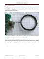
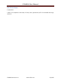
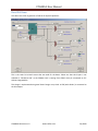
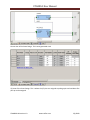
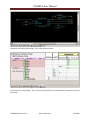
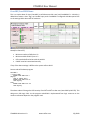
STAMP60 User Manual Features Actel A3P060 Low Power FPGA 50MHz Oscillator One User LED 1.5V LDO Regulator for FPGA Core Supply Single 3.3V Supply 30 User I/O’s SMD or TH mountable Design Support Actel’s free Libero 8.5 design environment can be used to create own configurations. If CoreABC is used then CoreConsole 1.4 needs to be installed also. Programmer Support STAMP60 can be re-programmed using a JTAG programmer/cable. Either Actel FlashPro3 or 3rd party cable can be used. Please note that ProAsic3 FPGA’s can be reprogrammed maximum 500 times as per datasheet. This doesn’t mean they will stop working after 500 programming attempts, but the FPGA is not specified for a larger number of reprogramming cycles. Open source project UrJTAG (hosted at SourceForge) can be used to play back SVF files and program the FPGA. UrJTAG supports many different JTAG Cables. STAMP60-UM version 1.0 www.trioflex.com 2/1/2009 STAMP60 User Manual Mount styles The module can be mounted in different ways, either using pin headers or then as SMD component by direct solder. Name SIP DIP QIP SMD Mount Type TH TH TH SMD Max User I/O 6 14 26 30 SIP Mount For this style of mounting only the left row (pins 1 to 8)can be used, number of useable I/O is 6. Pins 1724 can be used as user configuration switches or header. DIP Mount For this style the left and right rows can be used. Total amount of useable I/O is 14. CAD Component 3D view, 8 pins in 2 rows at 700mil distance QIP Mount For this style all TH rows can be used, total amount of useable I/O is 26. SMD Mount For this style all SMD pads can be used, total number of useable I/O is 30. STAMP60-UM version 1.0 www.trioflex.com 2/1/2009 STAMP60 User Manual On-Board Components STAMP60 is mounted with the minimum set of components to make it easy to use while still keeping the cost low. For OEM orders there is a possibility of some custom assembly options. FPGA The main component on STAMP60 is Actel ProAsic3 family low power Flash FPGA A3P060-CN132. Feature Number of Logic Cells 1536 Number of Block RAMs (512x9 bit) 4 Number of CCC (Clock Conditioning Circuit) 6 Number of PLL’s (CCC’s with PLL) 1 VCCIO for all banks and VJTAG/VPUMP are all tied to the single VCC pin that should normally be connected to 3.3V supply voltage. Oscillator A 50MHz Oscillator is mounted as default on the STAMP60. The oscillator is always enabled, it’s output is connected to FPGA pin A26. Note that while A26 is Global clock input, it is not connected to CCC with integrated PLL. So when using a PLL the clock to PLL input must be routed using other global clock lines (not using the PLL own hardwired input pads). User LED One Red color LED is available on the board, it is “On” when FPGA Output is logic 1. Connection to FPGA pin A37 via 1K series resistor. Note that the LED will be “dimmed On” while programming the FPGA, this due to the pull-ups that are normally enabled during the programming. STAMP60-UM version 1.0 www.trioflex.com 2/1/2009 STAMP60 User Manual FTDI Support STAMP60 can be used in different ways with the FTDI USB devices. Clock generator STAMP60 can deliver 6MHz clock for the older FT232/FT245 devices and for FT2232. So the BOM is reduced by 2 Capacitors and a Crystal. 93C46 Emulation Serial EEPROM can be emulated, including the resistor that is normally needed for the connection to FTDI devices. So the BOM is reduced by 2 components (1 resistor and 93C46 EEPROM). User Logic Different user logic can be implemented by the STAMP60. STAMP60-UM version 1.0 www.trioflex.com 2/1/2009 STAMP60 User Manual CAD Support Libraries are available for several popular CAD tools. STAMP60-UM version 1.0 www.trioflex.com 2/1/2009 STAMP60 User Manual Demo Designs List of available demo designs, supplied as Libero projects, with full source code and ready to download programming files. LED blinker A simple clock divider makes an human eye visible blink on the LED from the on-board 50MHz oscillator. STAMP60-UM version 1.0 www.trioflex.com 2/1/2009 STAMP60 User Manual FPGA Oscillator Test This is a simple design that demonstrates the use of an oscillator made from FPGA primitives. The CLKDLY primitive is used, also one global I/O pin. The frequency can be set by selecting the 5 bit delay parameter. Please note that the delay cannot be changed dynamically, it has to be fixed during bitstream generation. The demo will blink the LED at rate fosc/224, the output clock of the oscillator is available on pin 2. All other pins are not actively driven (configured as inputs). The oscillator is configured to lowest frequency (delay code 11111). The LED blinks at about 2 Hz rate. In the demo design the clock output pin is the same pin used in the oscillator as part of the loopback, so the capacitive loading on this pin will change the frequency. For real designs some free unused pin should be used instead. For best temperature stability the lowest frequency setting should be used, because then most of the delay is introduced by the CLKDLY primitive and the I/O pad parameters have less impact on the frequency. For STAMP60 there is no reason to ever use this type of oscillator, as the module has on-board oscillator. This design is provided as demonstration only. In some ultra low cost designs this type of oscillator maybe sufficient if exact clock is not needed. This demo is implemented as single VHDL file, the I/O constraints are entered in the Designer I/O Editor. STAMP60-UM version 1.0 www.trioflex.com 2/1/2009 STAMP60 User Manual Source code for the On-Chip Oscillator Demo ----------------------------------------------------------------------------------- Company: Trioflex OY http://www.trioflex.com -- Engineer: Antti Lukats ---------------------------------------------------------------------------------library IEEE; use IEEE.STD_LOGIC_1164.ALL; use IEEE.STD_LOGIC_ARITH.ALL; use IEEE.STD_LOGIC_UNSIGNED.ALL; -- we need ProAsic3 technology primitives library proasic3; use proasic3.all; entity top is Port ( en : in STD_LOGIC; -- must be connected to GND (or use pulldown) clkout : inout STD_LOGIC; -- must be global clock capable pin LED : out STD_LOGIC ); end top; architecture Behavioral of top is component CLKDLY port( CLK : in std_logic := 'U'; GL : out std_logic; DLYGL0, DLYGL1, DLYGL2, DLYGL3, DLYGL4 : in std_logic := 'U') ; end component; signal prescaler: std_logic_vector (23 downto 0); signal gl: std_logic; begin -- Divide the clock for Eye visible blink rate process (gl) begin if (rising_edge(gl)) then prescaler <= prescaler + X"000001"; end if; end process; -- drive the LED LED <= prescaler(23); -- en is a pin that is externally connected to GND so we use it as known const 0, but synthesis -- doesn’t know this, so the bibuf will remain in the code (is not optimized away) clkout <= (not gl) when en='0' else 'Z'; -- we need an inverter to make it oscillate! -- the CLKDLY primitive InstCLKDLY : CLKDLY port map( CLK => clkout, GL => gl, DLYGL0 => '1', -- set the frequency DLYGL1 => '1', -- 1111 is the lowest setting DLYGL2 => '1', DLYGL3 => '1', DLYGL4 => '1' ); end Behavioral; STAMP60-UM version 1.0 www.trioflex.com 2/1/2009 STAMP60 User Manual L( C ) Oscillator Demo L(LC) oscillators seem to be fully forgotten art, but they may have a new second life for some applications. Philips (now NXP) Application Note AN456 is a good description how to implement LC oscillator for MCU clocking. An logic can also be used to implement a LC oscillator, actually all we need is a single inverter connected to I/O Pins. LC Oscillator test, STAMP60 rev A is used. There are no C added so only the pin capacitance is working as part of the LC circuit. For real designs some extra C should be added. The L can be implemented as PCB spiral inductor so it cost is very low. Another interesting application would be using PCB inductors for touchless inductive sensor. Microchip has lots of information how to implement inductive touch sensors using Microchip PIC microcontrollers. But an FPGA could do the same with almost no extra circuitry, it is sufficient to make the sensors to oscillate and measure the frequency change. Extra analog circuitry should not be necessary. STAMP60-UM version 1.0 www.trioflex.com 2/1/2009 STAMP60 User Manual RISC 5X SoC Demo In preparation A RISC Core compatible to Microchip 5X family takes approximately 50% of the A3P060 FGPA logic resources. STAMP60-UM version 1.0 www.trioflex.com 2/1/2009 STAMP60 User Manual Fixed PLL Demo This demo uses a PLL to generate a fixed set of output frequencies. This is the static PLL wizard screen that was used for the demo. Please not that clock input is not selected as “Hardwired I/O” as the 50MHz clock is coming from Global clock pin connected to CCC without integrated PLL. This design is implemented using Actel Smart Design as top level. A LED (with divider) is connected to the GLA output. STAMP60-UM version 1.0 www.trioflex.com 2/1/2009 STAMP60 User Manual Canvas view of the Smart Design. This is auto generated view! I/O view of the Smart Design. This is where the I/O pins are assigned to package pins and attributes like pull-up can be assigned. STAMP60-UM version 1.0 www.trioflex.com 2/1/2009 STAMP60 User Manual Schematic view of the Smart Design. This is auto generated view! Grid view of the Smart Design. This is where the connections are made between components and top level ports. STAMP60-UM version 1.0 www.trioflex.com 2/1/2009 STAMP60 User Manual CoreABC/CorePWM Demo This is a simple demo for Actel CoreABC (a soft Microcontroller core) and CorePWM IP’s. A divider is added that creates a slow “flag” on CoreABC input port0. CorePWM is configured with Max period 255 so the settings 100 is about 40% of maximum. Notes(For Libero 8.5): Minimum number of APB slots is 2 Minimum width of INPUT port is 2 LED must be defined as bus with the width 1 CLKINT must be instantiated manually If any of the above settings is different the system will not build. Source code of the demo program DEF PWM0 0 // Enable PWM0 APBWRT DAT8 PWM0 0x08 1 $MyLoop JUMP IF INPUT0 $Set1 APBWRT DAT8 PWM0 0x14 50 JUMP $MyLoop $Set1 APBWRT DAT8 PWM0 0x14 100 JUMP $MyLoop The above code will change the LED intensity from 20% to 40% at slow rate (controlled by INPUT0). This design uses 249 Logic Cells. As the program code ROM is implemented from logic resources so the resource utilization depend on the program used. STAMP60-UM version 1.0 www.trioflex.com 2/1/2009