1
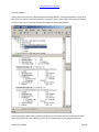
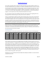
Antti-Brain Issue 4 December 2008 http://www.antti-brain.com Revised on December 25, 2008 Editorial Merry Christmas! Releasing December issue a little earlier, so can work on the January one. Releasing before proof-reading, sorry folks, time is precious at the moment. Antti Lukats [email protected] http://groups.google.com/group/antti-brain Antti-Brain 11/2008 Page 2 http://www.antti-brain.com Cover Story Some examples how to use the Happy New Year 2009 Adapter PCB. One picture, tell, eh why only one? The PCB was designed to be given away to be cut apart, it has some nice collection of SMD footprints on it. It is condensed design, so the fan-out pads are rather small, but it still is useable with thin wires. QFN-32 Pin package, Atmel AVR ATmega8 TQFP-32 Pin Package, Atmel AVR ATmega8 TQFP-80 Pin Package, ASIX Ethernet MCU SOIC-14 Pin narrow body. SOIC-16 Pin, wide body. TSOP-32 wide, SST NOR Flash. SC-70-5 and TSOP-14 Packages. Antti-Brain 11/2008 Page 3 http://www.antti-brain.com u-TSOP-10 Package, Maxim LDO regulator. TQFP-144 Pin Package, Lattice Flash FPGA. TQFP-128, Genesys Logic PCIe to PCI bridge, hum only as footprint demo, I think it not wise to try PCIe on the single sided proto PCB. The PCB has some more footprints, not all possibilities are shown. Antti-Brain 11/2008 Page 4 http://www.antti-brain.com Amontec USB-Tiny First impression is discouraging, I failed to find a user manual or datasheet for the device at the manufacturers website, there are several single page PDF files, but not a single easy to download file with all relevant info. So you need to download all those small files separately. Those small single page files include a footnote: please consult “the datasheet of the Amontec JTAGkey”, well that datasheet is the one I have never found. Antti-Brain 11/2008 Page 5 http://www.antti-brain.com Testing with Xilinx FPGA First I look the pin-out, ok I need connect GND and VREF, it seems that there is multiply pins for GND, so I choose one of them, pin 4, and pin 2 for VREF. Then I run Amontec demo application. And well, I see nothing useful returned from the scan. Also I notice the green LED is not on. Unfortunately there is no VREF read-back indicator in the Amontec Demo. I try turning on the Yellow LED, it is shown in the schematic as being connected to the FTDI chip, and LED power is derived from ‘1’ not from VREF (so I assume). Well the yellow LED doesn’t ever turn on. Next round of manual pages decoding. Ok, let us try pins 1 and 20 for GND-VREF! And voila now the green LED is on, and yellow LED can be controlled as well. Quickly I connect the JTAG pins as well. And click DRSCAN, and voila the Xilinx JTAG ID is read correctly: Antti-Brain 11/2008 Page 6 http://www.antti-brain.com Now let’s try the SVF Player, I start the demo bat file, and well it happily reports that the chain is scanned ok, gives the JTAG ID code that was found. Launching ISE, making dummy top VHDL, impact, generate SVF, running SVF player –sf top.svf Reported time 803 milliseconds, the done LED on the FPGA goes on, so the FPGA was really configured ok. How nice, it works! Ok, time to proceed to the next test, Actel FPGA Testing with Actel FPGA I open FlashPro manual, connect the flying leads. Running SVF player with ERASE_ALL.SVF (for A3P060), 52 seconds, success! Now let’s program the device, 112 seconds, success. Did it program ok? Running now with VERIFY.SVF file to check the programmed device is really programmed. this time comes SVF check error, means the device is correctly programmed. Says error on SVF line 154, lookup there says it the first row to be verified. So it looks the device did not at all get programmed. Proceeding with troubleshooting. Generating new SVF files with Libero 8.5, and going to test the programming functions one by one. Running erase SVF, error on line 220, execution time 52 seconds. Second run, same error. Line 220 is first scan check after the actual erase, so failing there means the device is not erased correctly. But the erase SVF from previous Libero version did not report an error? Right, I had tried the erased once on the empty FPGA, so it did check as erased (even if actual erase was not performed). Makes sense. But why Antti-Brain 11/2008 Page 7 http://www.antti-brain.com does the erase fail? The SVF execution time is correct, the erase delay in SVF file is 52 seconds. Let me try another power supply for the 3.3V maybe it helps. No, still same error. Ok, looking at UrJTAG project, they claim have programming Actel devices and also support the Amontec cable. But they have no precompiled releases, so I need to recompile it all from sources. Executing ./configure from cygwin shell, super it says has no C compiler. Right on this notebook it is not installed. So starting the cygwin update (in the hope it will not mess up the Xilinx install as it sometimes does). Eh it says C compiler (gcc) cannot create executables. In the log is “cc1.exe not found. Eh I just did install GCC? Ok, modifying cygwin.bat to set the path to cygwin. Now it goes little further. Oh god, now it detects something, but says cannot support USB devices. It’s such a pita when the releases are source only Ok, need install all the missing tools and libraries. Configure finished! Typing make! Voila some exe files are slowly appearing! And the JTAG.EXE even starts and prompts greeting. Well for the use with Amontec JTAGKEY I still need those missing libraries and a fresh recompile. Running cygwin setup again, pulling in libusb. Rerunning configure. Ok, libusb detected, now hopefully only need lib for FTDI. Downloading libftdi, running configure. Eh this IS confusing: I want libftdi, but it requires me to install libconfuse also! Great! I wonder how long I need keep downloading and installing stuff. Configure still running, let’s see what it says. Nice the confuse thing seems to include windows build. Ok, downloading that now. Oh, no C++ fails sanity check. Hope this all doesn’t drive me insane. Ok, running again cygwin setup to pull in C++ compiler. Configure on libftdi ok, running make. Also success, make install, also ok? This is confusing, I haven’t installed the libconfuse yet, so I was expecting to see some error with the libftdi. But no error, it even reports support for FTDI low level now, but Amontec support is still not compiled in. Trying to install the libftd2xx now. Hum, what to download? WinXP or Linux version? Windows is already installed, so I download the Linux version also. But where is the library source code? I need ftd2xx library. There are prebuilt .so files for Linux, but those can’t be used on windows. Hum.. looking at the config log, it tries to build a C test program, that calls FT_OpenEx(), well that should be possible with the windows drivers also. Ah need more RTFM , there is a way. Running again the configure for the UrJTAG main package with the required option. YES! Configure didn’t complain, running make again. Success! Running JTAG.EXE, type SVF ERASE.SVF And? Stack dump! Access violation. Eh, no luck today. Ah, I see, I need to-do even more RTFM, must do cable connect first. OK, trying again: >cable JTAGkey >detect Now it doesn’t do stack dump, just freezes. It did say it uses FTD2XX before it, so I assume it was configured ok. Well there is no message about any problems just freeze. Unplugging the JTAGkey from the USB port. Same result. So I don’t even know if UrJTAG ever tried to access the hardware are all. Getting some advice from the UrJTAG developer, but it related to BSDL files, and I don’t even get that far yet. I suspect that Amontec driver prevents the libftd2xx driver to connect to JTAGkey from UrJTAG, but I am not sure. I definitely do not want to re-install Amontec drivers just to run UrJTAG. Antti-Brain 11/2008 Page 8 http://www.antti-brain.com Recompiling FTD2XX with DEBUG on, now I see lots of debug print, mostly saying there is never anything read. But also no error or something. Eh, I have 2 FTDI gadgets connected to this PC, so to which one the UrJTAG connects? I disconnect the dummy gadget (that I used to get 3.3V from PC), and now the UrJTAG unfreezes so it was connecting to wrong device. [censored] So it was! It was always connecting to FT245RL cable, not to JTAGkey! Typing detect and print, and voila: it does see the A3P060QN132, the right device. Trying SVF execute, and now we have still error: “could not establish SIR instruction” ? I better remove the debug from the code, so it will be less noise on the screen. But this is now weird, after running the ERASE.SVF with UrJTAG a few times, I did run again Amontec SVF player, and this time it reported erase success!! Ok, I just got response from the UrJTAG author that there is a problem identified, and problem report created in the bug tracker. And this within hours since I stumbled onto the problem. On Sunday! Ok, so it better for me to not that UrJTAG on Actel till the problem is solved. But, erase succeeded with Amontec player, so let’s try again the program/verify cycle. Program success in 131 seconds. Verify? 33 seconds, and success? Did it really work this time? Verify says that FPGA array is verified and OK. Does it work a second time? Executing erase, success running verify error, well that’s good Running again program array, error Trying, trying,.. no more luck. Erase gives error, and if not then programming does. Until, well now the FPGA seems to be dead. The LDO for 1.2V core supply gets hot very quick and the JTAG does not scan the ID code any more. So is this first time I have managed to destroy an FPGA using JTAG? Seems so. I did not touch the FPGA or cable or power supply during the testing, so it could only be that bad FPGA programming sequence destroyed it. Next day: UrJTAG problems have been fixed in the SVN code, but compiling the SVN checkout version under Cygwin is even more complicated then the release code compilation. So I haven’t yet succeeded with it. Actel WebCase response comes also about my SVF issue, but they only ask for additional information. Trying again to compile UrJTAG, one problem with autogen.sh was Perl saying fatal error because remap problem with GLOB.DLL ?? Nice, well short Google search does help some magic. I exec ash and type /bin/rebaseall No trying again autogen.sh, it seems no errors now, let’s see how far it goes. It’s is all running, but now I still need to figure out how to make the autogen to see the ftd2xx library, as otherwise there would be Antti-Brain 11/2008 Page 9 http://www.antti-brain.com no support for the JTAGKey. Ok, it does run till fatal error saying “Makefile.in” not found, well the file is there, but it looks the script thinks there is carriage return char in the filename? Well whatever it is failing. Hum, it looks the SVN checkout changed text type to dos from unix, so the configure.ac includes CR symbols that propagate into the filename! Yes, now the build completed! If I only could again enable the FTD2XX drivers again into the build! Next day: Actel support asked another meaningless question. UrJTAG team prepared ready build version for testing, and plans are made to supply precompiled binaries for Windows platform. << to be continued >> Antti-Brain 11/2008 Page 10 http://www.antti-brain.com SiliconBlues Xilinx BLU Stories Things that go wrong with Xilinx devices and tools. No drivers license! Debugging with XMD, it worked somewhat, then suddenly “invalid device driver license” error. Looking up AR’s, and voila, answer is there, it only happens on Windows Vista (the only O/S that is available for purchase with new PC’s), and it is fixed in ISE 9.2SP2! Great! I am using ISE 10.1SP3, so the problem reappeared? Or do I need new drivers license? My license is valid in the EU to my best knowledge. + or - ? A developer at nearby company doing RF stuff needed some FPGA design to be done quickly. So I looked on my desk what is the easiest for him to get started. Aha, Xilinx (made by Digilent) Spartan-3A starter kit (it has on board USB JTAG cable portion). I say here, take this. Just plug in USB cable and work with Xilinx tools. I look around for power supply. Do you have 5V supply? Yes sure. Ok, then here you go. I assumed he will just plug in the cables and it all will work. It was Thursday afternoon. Next Monday comes email, your board is dead, there is porridge(youghurt?) around the on-board power supply IC’s. Hum, yes there is, know, I was too lazy to wash the board, but it WAS working, definitely. What’s could they have done with the board? Is it really destroyed already? A little later I get update, the board takes too much current, power supply hits current limit. What? How come do they know that if they use standard 5V DC wall plug power supply? Well, they say we could not use standard power supply because the board has “–“ terminal connected to the inner contact and the outer shell is “+” and all our PS have different arrangement! What, that’s not true I say, this board has STANDARD power, “+” is inner contact. No they say, we looked, it is printed on the board! We looked under magnifier glass, we are sure, inner is negative ! No, no, it Is not so! Ok, I take some power supply (standard 5V ones) and go them. I look the PCB board from Digilent, and yes, it reads clearly that “–“ is inner terminal. So I take my supply where “+” is inner and plug it into the Xilinx Starter kit. The power LED goes on. I press reconfiguration button, prog_b LED goes off and on again. It is all working! …! I am really pissed. I am not a fan of Digilent, but such a stupid thing? I couldn’t almost believe it, but seeing is believing. Anyone who uses his own eyes, and connects Xilinx S3A Starter kit board to power supply by the markings on the board itself, would destroy the board if the power supply is powerful enough! A full work day wasted with the Digilent power supply troubleshooting. Antti-Brain 11/2008 Page 11 http://www.antti-brain.com Controller Corner This is also not “getting started for dummies”, sorry about that, the sections was about to remain empty, so wrote down some struggle I had. SiLabs MCU’s Part II Today I got PCB’s for my next project using C8051F321, so I wanted to test it very quickly. Plugging in the micro-USB cable. A LED is little-bit lit, good seems power is OK Measuring voltages on the LED, 1.5V, and same voltage is on the other side of the LED current limiting resistor also. Seems I have a very good LED that takes very little current, so it is LIT on the port pull-up resistor already. C2 programming interface needs only 3 wires to be connected, so it is only 8 possibilities to make it wrong? Well I managed to fix my wiring more than 20 times before SiLabs IDE reported successful connect. Doing it fast isn’t always the fastest way to get things working! Downloading HID Blinky firmware, USB device is seen, but it listed as unknown device. Oh, no did I manage again to get the USB connector pinning wrong? Hope not, but what could cause the USB device enumeration to fail? Looking at the PCB, ah, there is solder bridge below the connector between DP/DM! It’s really not so easy to get the solder off from those pins, but with some flux I manage it. Trying again, yes! It’s working now, I start HID Blinky PC demo application, yes it can connect ok. So looking at my schematics and modifying the HID Blinky firmware for the LED connection. Done, download ok, trying out the blink sequences. Hum.. seems the Blinky firmware uses PWM value more than 0 for OFF, because the LED blinks between max (or PWM set value) and some low intensity value. This is annoying, OFF should be OFF, so I need to find a good resistor value. Here the LED is at max intensity. To the left is 300mA SOT-23-5 packaged LDO, to the right is 3-Axis Acceleration sensor. Antti-Brain 11/2008 Page 12 http://www.antti-brain.com USB Bootloader SiLabs USB MCU’s do not have built in USB update firmware, so if firmware update over USB is desired it must be implemented by the client application loader. Ok, there are several options for the Bootloader. I had a HID based Bootloader for F326, written for IAR C form an previous project. So I am trying this (now for F321). Compiling with IAR, got it compile, downloaded to the device, but it doesn’t enumerate. Hum.. trying to launch debugger form IAR EW, but it ask to reprogram the debug adapter, well this is something I do not want to-do as it is already flashed with the latest SiLabs firmware (IAR possible is just using older version!). Ok, looking IAR project options to make it generate HEX file so I can use SiLabs IDE to download to target. Ha, this is tricky, I have to select override, and change file extension from d51 to hex. This will also change the file format! Hum, no, it does still make wrong format. Ha, there is format selection Selecting Intel-standard (hex). Compiling HID example (for F321) with IAR, downloading with SiLabs IDE – USB enumeration OK. OK, let’s be brave, I let IAR to reflash the debug adapter, and start debug session. Source code debugging not available , hum I try change project options to include debug info in output file, starting again C-SPY, now it freezes, and says no response from target. Ok, this lines up with my previous IAR experience, the SiLabs debugging is available, but has problems. Reverting back to SiLabs IDE, it now again reprogram the debug adapter of course. Another possibility, I make new project with SiLabs IDE and select IAR as toolchain. Let’s ok compile assembly ok, but linker cannot find its script file. Well this is encouraging. Ha, first Google hit returns relevant document – IAR integration with SiLabs IDE! AN236 from SiLabs, this is why this information was not in the SiLabs IDE help file where I looked for it! Well, it didn’t help, but I see something weird, the path to linker is correct, but the command line options include path to the where the linkers scripts are is truncated! Well this is not my fault as it auto generated by SiLabs IDE. Ha I tricky a little, I create a folder with the truncated name, and place the linker script there. Yes, now the linker sees the file, and well it gives now syntax error, but this is possible because of the version difference. Strange still as the iarbuild did use the same linker, hum, maybe it did also use wrong linker file. Need to check it out! After commenting out the error lines in linker script, I get error: Error[e12]: Unable to open file 'cl-pli-nsid-1e16x01.r51' I guess it same issue with the truncated linker paths. Yes so it was now I get NEAR CODE segment problem, but this may be because I did not properly fix the link script. Trying with the default script from IAR toolchain. Hum it still doesn’t succeed. RTFM ,well AN236 applies to SiLabs IDE version 2.90 and IAR 4.05, but I have IDE 3.42 and IAR 5.0! Hum, AN236 PDF say the supplied software includes a fixed linker script, but that download cannot be found. Ok, I revert back to the linker script that was used with the project (that works with IAR build tools!). I see now, when I select no code optimization in IAR it also can not fit the code. So all I need now is to set Antti-Brain 11/2008 Page 13 http://www.antti-brain.com the optimization for the build from SiLabs IDE. Too bad IAR EW doesn’t show the compiler build switches. Ah it does, in some map file produced there is full command listed as well. Adding –Ohz to the Compile options in SiLabs IDE toolchain integration dialog. And now it compiles and links Ok! Trying to download from SiLabs IDE but it complains no file found, ah need some extra step to make hex file I guess. In target build configuration is edit box for executable to generate hex file. What should I enter there? Some IAR tool? No, nothing needed just had to enter the file name of the IAR linker output (with extension A51). And now I see the IAR compiled code to run in the chip, the source code and disassembly window are updated in sync with the code execution. And the problem is also seen already, for some reason it resets in the loop, so the code handler is never reached. Sure question is why? Did you already guess it? The key here is that I used project initially made for F326, but with minor retargeting for F321 device. Doesn’t ring the bell? Ok, some more hints: F326 does not have watchdog timer. Yes, F321 has and it is enabled after reset. So if the code doesn’t reset it, then the init code has to disable it for good. If not then any code will be restarted in loop by the watchdog reset! [censored] All the trouble I had, and the reason was I forgot to add the watchdog disable when converting the project from F326 to F321! Ok, I learned the IAR integration to SiLabs IDE on the way. I start the HID FW Updater PC application, and yes it sees the F321, it listed as “FW Update” device! But oh no, my FW update application does NOT work, so still some troubleshooting ahead. Now, this is awful, USBview used to be easy to download, but not anymore, had really hard times to find, it, and eh it doesn’t show much anything, eh I wanted HIDView! Even worse, not available, the USBCV I cannot use as my notebook has OHCI controller not EHCI. Ok, getting Delphi sources for HIDtest and compiling them. This all after lots of troubleshooting and snooping with USB Snoopy. Not much useful info either. This is weird something must be wrong with the Input Reports, but I cannot figure out what. It could also be a problem with the PC software, when I try it using USB Blinky Firmware in the F321, I can successfully send reports that change parameters, but reports retrieving data back fail, and USB Snoopy doesn’t show any activity either. Really strange, the functions return with error: no error ? What I do know that the FW Updater host software DID WORK on Win XP host when the chip was F326, no I am have Vista notebook and device is F321, and it isn’t working. Hum, maybe I should create Delphi headers for SiLabs HID DLL and use that instead of the Delphi native HID component? Because the SiLabs host application demo code works. I could of course rewrite the host app to C, but I haven’t almost ever written PC GUI applications in C, so I leave this as last option. Already converting the C header, when I discover that it is C++ library exporting a Class, this is something I do not want to call from an Delphi application. The attempt to compile the SiLabs host C code also failed, as I do not have all C libraries needed installed. Today is 24th of December, maybe it’s time to get a piece of peace. Antti-Brain 11/2008 Page 14 http://www.antti-brain.com Yes something must be awfully wrong, when I press a button to read statistics, then I see USB activity in USB Snoopy log This was called from C as: HID_Blinky.GetInputReport_Control (OutputEnableBuffer, HID_Blinky.GetOutputReportBufferLength ()); But when I try from Delphi code CurrentDevice.GetInputReport(Buf, 3); Then there is no USB Activity logged at all, so my F321 firmware naturally cannot respond either. Hum, but when I try my old pre-compiled FW updater? It used to work and is not been recompiled. Antti-Brain 11/2008 Page 15 http://www.antti-brain.com Next Day, USBlyzer: Getting some more test tools, downloading and installing USBlyzer, it does get detected as Trojan Virus, but I am brave and let it install and disable virus checkers. Now, it seems that it does show info little bit more accurate, here is screenshot showing descriptors of SiLabs debug adapter: As see the Endpoint descriptors are both showing correct information, but when looking at the same device using Microsoft’s own USBView, we see the second descriptor showing bogus fields, here: Antti-Brain 11/2008 Page 16 http://www.antti-brain.com The second endpoint definitely does not have maxPacketSize of 1287 bytes! So it seems old tools (pre Vista) do not work correctly on windows Vista. My FW updater was never tested on Vista, so maybe there is something different that prevents it to work properly. I am trying to use USBlyzer to debug the problem further, but it is very frustrating, USBlyzer freezes very quickly, and cannot be restarted without full O/S reboot. When it worked and logged transactions, the only thing I noticed there was never a event when I issued Input/Output reports to my Device, only a Write caused a event to be logged. What is even worse once started the USBlyzer seems to mess up the system very badly, SiLabs debug adapter is no longer found, and my own tools to work with HID also fail to see any HID devices. But USBview still list those HID devices as operational. Time to rethink. What options I have? Getting a PC with EHCI USB Host and run USBCV suite? Not possible on the notebook, I guess there are no EHCI adapters for Express-card slot available. Trying the same software with win-XP? Again, cannot do today, besides it has to work with Vista anyway. Downloading all the MFC libraries, and trying to recompile SiLabs host application? Using the VC and recompile a wrapper around SiLabs C++ DLL converting it to plain C DLL so I can interface it from Delphi? Trying out Atmel HID DLL? Buying a real hardware USB Analyzer? Or giving up HID and use USBXpress? Or partially give up HID and use libusb drivers? Or? Antti-Brain 11/2008 Page 17 http://www.antti-brain.com Or try harder, and harder! And..so stupid, the Delphi HID support hasn’t been update for long time, so the code has DEFINE switches up to WinXP, set as default to Win98Gold (whatever that was). I set them to the latest Win version available, but nothing changes. And then I look again the code, there is also a runtime check for Windows version, checking for VerMaj>=5 and VerMin>=1, Well WinXP is maj 6, min 0, so it fails this check and HID_GetInputReport and HID_SetOutputReport are just not linked with my program, this also explains why the old precompiled executable does not work! Ok, so far so good, I fix the runtime windows version check, but now I get as far as getting CRC errors, what possible are somehow wrong error code, as there can be no CRC error. Finally, it all actually works as desired. Both input and output reports can be used. I still need a little to complete the PC side firmware updater software, but the USB communications seem to work. The F321 simple HID update code it uses only 2 HID reports, ID 1 for Output and ID 2 for Input report. When wrong ID is used then for some reason the HID library returns with CRC error, it did confuse me at first. So I did not bother to check which ID must work for Input report, I assumed that same ID’s should work for both Output and Input Reports, what happened not to be the case. Folks, don’t ever try something to get working very quickly, I tried… the result is described above. At the bottom line there was not so much wrong with the code I used. But the way to find it out was really troublesome. I would have preferred to be with my family. Today is 25th December, wide and kids are in the country house (to let me work in peace). Selecting USB MCU SiLabs has basically 3 sub families with USB function, some comparison is given in the following table Device Package Fmax MHz Flash Endpoints UART Watchdog ADC VIO Pin 320 LQFP32 24 16K 3 1 Y Y 321 QFN28 24 16K 3 1 Y Y 326 QFN28 24 16K 1 1 N N Y 327 QFN28 24 16K 1 1 N N 340 TQFP48 48 64K 3 2 Y Y The 34x has more derivates not listed, also features common to all are not included in the table. F326 is special in that concern that I has separate pin for VIO supply. I did think hey this is truly nice to make USB-JTAG dongles. So I designed 2 different PCB for Actel and Altera compatible headers. And well those products still are not in production as the nice idea didn’t work out so well. The problem is that the VIO supplies also the RST pin, so if the VIO is left unconnected (in my case it goes to the VREF in the JTAG cable) then the MCU will not wakeup ever. Not even when the VIO is supplied later. So my cheap dongles would not work if the target system is powered after plugging the USB cable, but in that case VIO would appear before the main VCC, what is not good either. I did not see any easy solution for this, so those products are suspended. They would work if I tie the VIO to 3.3V permanently, but hey then what is the idea of using F326 in the first place? F320/F321 is the only sub family that has both QFN and non QFN parts available. It is also has the best price/performance ratio. Antti-Brain 11/2008 Page 18 http://www.antti-brain.com 34X parts that support 48MHz clock are of course nice, they have 2 UARTs and their SPI works at 4MHz in slave mode (compared to 2MHz for others). But the pricing is not so nice any more, I mean at 34X price level there may be reasonable to use some cortex USB micro already. So which one? If hobby project then LQFP package is easiest to solder, if small qty, (price not matter) then 34x in LQFP32 is easiest, or 34X TQFP48 has most pins while still being relatively easy solderable. Antti-Brain 11/2008 Page 19 http://www.antti-brain.com 3-Axis sensor testing Finally I have the small BGA-8 adapter connected to Sipsik™ header breakout. So I plug it into the CPLD adapter for DS. Here is how it looks. The blue cartridge has only XC9572XL inside, connected to the slot bus and reprogrammable in system. Running Xilinx XSVF player for DS, configuring the CPLD as GPIO. Creating new C code project, writing bit bang SPI routines. Takes no time – I usually find it easier to implement SPI as bit bang software then trying to use some dedicated SPI hardware. Looking at the datasheet, how nice there is WHOAMI command, with all bits 0, so it if the command is even shifted in wrong I should still see the response. And it works, I get some response back! Well I had managed to make 3 different errors in the SPI command functions, but for WHOAMI (0x00 command) they did not matter. It did take a short testing to get actual XYZ readings working as the sensor is place into power down mode after power on, and it will read 0 from most registers. The photo shows just first test where the readings of all axis are displayed on screen. Antti-Brain 11/2008 Page 20 http://www.antti-brain.com Inductive Touch Available from Microchip is “Inductive Touch Resource Kit”. Separately downloadable are some other files as well. The application notes referenced in the downloadable webinar document are not downloadable from the web, but they are included in the resource kit (only accessible after installation!). Reference design A reference design is provided, including schematics as PDF document, Gerber/NCDrill files and C code for Hitech C compiler. Compiled hex files are not available. Reference PCB – 2 layers, the inductors use 6 mil track/space. USB connector only for 5V. Components PIC16F886 MCP6001 x2 (single op-amp) Analog muxes: 2to1 and 4to1 types BC848C x2 BC858C x2 Big fat red warning Microchip claims the technology can be used with any PIC® or dsPIC® device, but actually it is only useable with devices that include ADC, and in all cases lots of external circuitry is required. And please review the license when installing the resource kit. It is all free of charge when you use Microchip products. But only then. Antti-Brain 11/2008 Page 21 http://www.antti-brain.com DIY: Logic Analyzer Pretty much any modern Xilinx FPGA can be converted to a Logic Analyzer. The easiest to-do this is the use of ChipScope tools. While ChipScope is primarily used to monitor signals in the FPGA (internal signals) there is no restriction to use it for completely external signals only. That is we have an FPGA with no user logic except the ChipScope IP cores, and we use ChipScope analyzer to capture external signals. Step-by-step: Launch ISE, create new project, select target FPGA, create VHDL top level, add some signals, run core generator, select ChipScope IP, select ICON, press generate, run core generator, select ChipScope IP, select ILA, select options, press generate, open “icon.vho”, look for “Begin cut”, select, copy, open top VHDL file, paste, back to “icon.vho”, repeat, same for the “ila.vho”, now add wire to connect icon control port to ila, and connect external clock and inputs to ILA trigger port, add UCF file, specify pin/ball names for the clock and trace signals, run implementation flow, download to FPGA, start ChipScope analyzer. Done, you are running your own logic analyzer! Simple uh? But it really is! Ok, my step-by-step was a little condensed, so I add the example TOP file here: library IEEE; use IEEE.STD_LOGIC_1164.ALL; use IEEE.STD_LOGIC_ARITH.ALL; use IEEE.STD_LOGIC_UNSIGNED.ALL; entity top is Port ( clk : in STD_LOGIC; data : in STD_LOGIC_VECTOR (15 downto 0); dummy : out STD_LOGIC; led : out STD_LOGIC); end top; architecture Behavioral of top is component ila PORT ( CONTROL : INOUT STD_LOGIC_VECTOR(35 DOWNTO 0); CLK : IN STD_LOGIC; TRIG0 : IN STD_LOGIC_VECTOR(15 DOWNTO 0)); end component; component icon PORT (CONTROL0 : INOUT STD_LOGIC_VECTOR(35 DOWNTO 0)); end component; -- need add manually this signal signal CONTROL0 : STD_LOGIC_VECTOR(35 DOWNTO 0); begin -- dummy output to keep the input port in the desing Antti-Brain 11/2008 Page 22 http://www.antti-brain.com dummy <= '1' when data=X"FFFF" else '0'; -- simple test added (not part of the analyzer core) LED <= data(0); -- logic analyzer cores are bind here ila_1 : ila port map ( CONTROL => CONTROL0, CLK => CLK, -- connect to SYSTEM CLK PIN TRIG0 => data); -- connect SIGNALS TO BE ANALYZED icon_1 : icon port map ( CONTROL0 => CONTROL0); end Behavioral; Most of the code is either generated by ISE or copy-pasted. The only thing to take care of are the inputs they must remain in the design, so a dummy expression may be needed. In this example the analyzer has 16 inputs (it was specified when generating the ILA core). This design was created from scratch and demonstrated in the real FPGA within less than 40 minutes time. For demo I connected data(0) to push button and captured it with ChipScope. Here is the UCF files used (for GOP200 module) NET NET NET NET NET "data<0>" "data<1>" "led" LOC "led" LOC "clk" LOC LOC = "P27" LOC = "P28" = "P81" ; = "P81" ; = "P38" ; ; ; NET "clk" CLOCK_DEDICATED_ROUTE = FALSE; Antti-Brain 11/2008 Page 23 http://www.antti-brain.com This is how it looks in ISE before launching CS analyzer. The target board I used was XC3S200 DIP module from OHO-Elektronik. Antti-Brain 11/2008 Page 24 http://www.antti-brain.com Single Sided SMD break-out-boards ARE really nice Si4721 FM Radio Using QFN packages on 100mil proto boards is no fun? Or is it? Si4721 stamp-break-out style adapter is soldered onto the pads of 100mil SimmStick™ proto board. I had not previously soldered such cut-hole PCB adapters, and it was surprisingly easy. Solder flows nicely and the edge holes get soldered to the pads firmly. Soldering is pretty much as easy as soldering a DIP component. Ouch, I really can’t remember when I used a DIP component last time! Probably it was SiLabs DIP14 packaged test chip for the F300 family (this chip is no longer available). Antti-Brain 11/2008 Page 25 http://www.antti-brain.com References Amontec http://www.amontec.com Trioflex http://www.trioflex.com VTI http://www.vti.fi Instead of adding the URL links at the end of each issue, I will be adding them to the Trioflex online link collection, so they can be updated more frequently. Antti-Brain 11/2008 Page 26