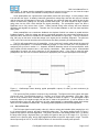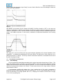
1
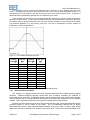
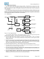
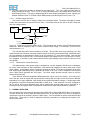
PX4 User’s Manual Rev A1 PX4 USER’S MANUAL Amptek Inc. 14 De Angelo Drive Bedford, MA 01730 USA PH: +1 781 275 2242 FAX: +1 781 275 3470 Email: [email protected] Web: http://www.amptek.com Amptek Inc. PX4 Digital Pulse Processor & Power Supply Page 1 of 27 PX4 User’s Manual Rev A1 Table Of Contents 1 PX4 Design and Operation ................................................................................................................3 1.1 Major Function Blocks...................................................................................................................3 1.2 PX4 Signal Flow............................................................................................................................5 1.3 PX4 Input ......................................................................................................................................5 1.4 Analog Prefilter..............................................................................................................................6 1.5 Pulse Shaping and Selection ........................................................................................................9 1.5.1 Pulse Shaping........................................................................................................................9 1.5.2 Baseline Restoration (BLR) .................................................................................................10 1.5.2.1 Auto-Baseline .................................................................................................................11 1.5.2.2 BLR.................................................................................................................................11 1.5.3 Pulse Selection ....................................................................................................................11 1.5.3.1 Pile-Up Rejection ............................................................................................................11 1.5.3.2 Rise time Discrimination .................................................................................................12 1.5.3.3 Thresholds ......................................................................................................................12 1.5.3.4 Gate ................................................................................................................................13 1.5.4 Multichannel Analyzer..........................................................................................................13 1.5.5 Multichannel Scaler .............................................................................................................13 1.5.6 Single Channel Analyzers....................................................................................................14 1.6 Power Supply ..............................................................................................................................14 1.6.1.1 HV Bias Supply Discussion ............................................................................................15 1.6.1.2 Thermoelectric Cooler Discussion..................................................................................15 2 Normal Operation .............................................................................................................................15 2.1 2.2 3 General Specifications, Connectors, and PIN OUTs ....................................................................19 3.1 3.2 3.3 3.4 3.5 3.6 3.7 3.8 3.9 3.10 4 General Specifications ................................................................................................................19 AMP IN (front panel) ...................................................................................................................19 XR100 Power (front panel) .........................................................................................................19 On/Off (front panel) .....................................................................................................................20 Digital I/O (back panel) ...............................................................................................................20 USB (back panel)........................................................................................................................20 Analog Out (back panel) .............................................................................................................20 AUX (back panel)........................................................................................................................21 PX4 Input Power (back panel) ....................................................................................................21 Ground (back panel) ...................................................................................................................21 Dead Time and Throughput in the Amptek PX4............................................................................21 4.1 4.2 4.3 4.4 5 Decimated Output .......................................................................................................................16 Auxiliary Outputs .........................................................................................................................17 Fast Channel...............................................................................................................................22 Slow Channel ..............................................................................................................................23 Acquisition Time..........................................................................................................................24 Timing Summary .........................................................................................................................24 Glossary ............................................................................................................................................25 Amptek Inc. PX4 Digital Pulse Processor & Power Supply Page 2 of 27 PX4 User’s Manual Rev A1 1 PX4 DESIGN AND OPERATION This section provides an overview of the design and operation of the PX4. The rest of the document assumes the reader is familiar with the terms and concepts presented here. This section assumes the user is familiar with the general principles and terminology of conventional nuclear electronics. 1.1 MAJOR FUNCTION BLOCKS The PX4 is a component in the complete signal processing chain of a nuclear instrumentation system, as shown in Figure 1. The input to the PX4 is the preamplifier output. The PX4 digitizes the preamplifier output, applies real-time digital processing to the signal, detects the peak amplitude (digitally), and bins this value in its histogramming memory, generating an energy spectrum. The spectrum is then transmitted over a serial interface to the user’s computer. The PX4 also includes several auxiliary logic functions, described below. The PX4 generates, from a single low voltage power input, the high voltage to bias the detector, power to operate a thermoelectric cooler, and the various low voltages required by the preamplifier as well as the PX4’s own circuitry. The PX4 replaces many different components in a traditional instrumentation system: the shaping amplifier, the multichannel analyzer, logic devices, high voltage power supplies, etc. Moreover, it has many more configuration options than a traditional system, e.g. many peaking (shaping) time settings. Outside of the PX4, all that is required is the detector and preamplifier, a computer with a serial interface and the software to communicate, and a low voltage power supply. Detector Preamplifier Analog Prefilter ADC Digital Pulse Shaper Histogram Logic Microcontroller Pulse Selection Logic Thermoelectric Cooler Supply Serial Interface Computer Aux Outputs High Voltage Suply Low Voltage Supplies +5V DC Figure 1. Block diagram of the PX4 in a complete system. Amptek’s PX4 has two main sections: a pulse processor and a power supply. The pulse processor has six main function blocks: (1) an analog prefilter, (2) an ADC, (3) a digital pulse shaper, (4) pulse selection logic, (5) histogram logic, and (6) interfacing hardware (which includes a microcontroller) and software. The power supply has three main function blocks: (1) a low voltage power supply (with several distinct output voltages), (2) a high voltage power supply, and (3) a supply for the thermoelectric coolers found in Amptek detectors. Analog Prefilter: The input to the PX4 is the output of a charge sensitive preamplifier. The analog prefilter circuit prepares this signal for accurate digitization. The main functions of this circuit are (1) applying appropriate gain, offset, and inversion (if necessary) to utilize the dynamic range of the ADC, and (2) carrying out some filtering and pulse shaping functions to optimize the digitization. ADC: The ADC digitizes the output of the analog prefilter at a 20 MHz rate. This stream of digitized values is sent, in real time, into the digital pulse shaper. Digital Pulse Shaper: The ADC output is processed continuously, using an FPGA with a pipeline architecture to generate a real time shaped pulse. The shaped pulse is a purely digital entity. Its output can be routed to a DAC for diagnostic purposes, but this is not necessary. The peak value of the digital shaped pulse is determined by a peak detect circuit in the pulse shaper. The peak value for each pulse, a single digital quantity, is the primary output of the pulse shaper. There are two different shaped pulses used internally. The first is the primary signal, optimized for the best signal-to-noise ratio. This usually has a long peaking time and is called a “slow pulse.” The second is a timing signal with much shorter duration and is called the “fast pulse.” These two pulse shaping circuits Amptek Inc. PX4 Digital Pulse Processor & Power Supply Page 3 of 27 PX4 User’s Manual Rev A1 constitute two different data processing paths or channels, operating in parallel to obtain complementary information. They are sometime termed the “slow channel” and the “fast channel.” Pulse Selection Logic: The pulse selection logic rejects (from the slow channel) pulses for which an accurate measurement cannot be made. It includes pile-up rejection (PUR): pulses may occur nearly simultaneously and result in a distorted measurement. The PX4 uses the fast pulse to detect and reject slow pulses which overlap. The fast pulse is used to measure the incoming count rate (ICR), which may be different from the count rate of selected pulses (the fast channel has much less dead time than the slow channel). The PX4 also includes Rise Time Discrimination (RTD) logic to reject from the slow channel pulses with a slowly rising edge. Each of these selection criteria may be enabled or disabled and has optional parameters, discussed in more detail below. Histogram Memory: The histogram memory operates as in a traditional MultiChannel Analyzer (MCA). When a pulse occurs with a particular peak value, a counter in a corresponding memory location is incremented. The result is a histogram, an array containing, in each cell, the number of events with the corresponding peak value. This is the energy spectrum and is the primary output of the PX4. The PX4 can also be operated in a MultiChannel Scaler (MCS) mode, where each channel represents time rather than voltage. Interface: The PX4 includes hardware and software to interface between these various functions and the user’s computer. A primary function of the interface is to transmit the spectrum to the user. The interface also controls data acquisition, by starting and stopping the processing and by clearing the histogram memory. It also controls certain aspects of the analog and digital shaping, for example setting the analog gain or the pulse peaking time. The interface includes a microcontroller and serial interface hardware. Both RS232 and USB interfaces are currently implemented and described in this manual. The PX4 also includes an FPGA which implements the pulse shaping and selection. The FPGA logic, the “FPGA Configuration Bitstream,” is copyrighted by Amptek, Inc. and may not be copied, modified, or used without the express, written approval of Amptek, Inc. Auxiliary Inputs and Outputs: The primary output from the PX4 is the spectrum, either the energy spectrum in MCA mode or a timing spectrum in MCS mode. There are also several auxiliary outputs and inputs. Many are useful for configuring a system or for debugging, while others are useful for special applications. These include DAC Output: The signal in the pulse shaper can be routed to a Digital to Analog Converter (DAC) and displayed on an oscilloscope. In software, the user can choose to display the shaped pulse, or the input to the ADC, or other diagnostic signals. The same signal sent to the DAC can be transmitted over the serial interface to the computer and displayed on the PC as in an oscilloscope. Digital Output: The user can route several logic signals to a digital output. This includes an Incoming Count signal (an indicator that a count is occurring), a pile-up signal, and several others. SCA Outputs: The PX4 includes eight discrete Single Channel Analyzers (SCAs). The user can set lower and upper level discriminators (LLDs and ULDs) for each of the eight channels via software. If a pulse occurs in this range, then a logic signal is sent to the SCA output. Auxiliary Inputs: The PX4 includes a GATE input, so that data acquisition can be gated with external circuitry, e.g. to synchronize with an X-ray tube pulse. It also includes a buffer control input. Power Supply: The PX4 is designed to operate from a +5 V DC supply (provided). It typically draws 0.5 A with an Amptek XR100, including a thermoelectric cooler. It draws approximately XA without the cooler. It will operate from DC voltages from 3.5 V to 6 V, so may be used with batteries or other sources. Low Voltage Power Supply: This supplies several different voltages, including +3.3 V to run the digital logic and +/-5 V to operate analog circuits. It also includes a supply which can be switched between +/- 8.5 V and +/- 5 V which powers the preamplifier and the first stage of the analog prefilter. High Voltage Power Supply: This provides the bias for the detector. It can provide up to +1500 V DC at a maximum current of 0.2 mA. The output is current limited, with 30 MΩ series resistance. Amptek Inc. PX4 Digital Pulse Processor & Power Supply Page 4 of 27 PX4 User’s Manual Rev A1 Thermoelectric Cooler Supply: This circuit provides closed-loop control of the one or two-stage thermoelectric coolers used in Amptek’s detectors. 1.2 PX4 SIGNAL FLOW The signal flow through the function blocks of the PX4 is illustrated in Figure 2. Trace 1 shows the input to the PX4, which is the output from an Amptek XR100CR reset-type charge sensitive preamplifier. The preamp has a gain of -1 mV/keV, so a 6 keV X-ray generated the -6 mV step seen here. This is processed by the analog prefilter, producing the ADC input shown as trace 2. This is digitized and then processed digitally, producing the PX4’s shaped output shown as trace 3. The peak of trace 3 is measured and the appropriate bin in the histogram is incremented. Figure 3 shows the result, the histogram of counts, which is the energy spectrum obtained by the MCA. The horizontal axis represents energy (amplitude of the shaped pulse) and is divided into 1024 channels, while the vertical axis represents the number of pulses with peak amplitude in the range of each channel, during the acquisition interval. Figure 2. Oscilloscope trace illustrating the normal operation of a PX4. Figure 3. Screen plot showing the energy spectrum, the histogram of pulse heights, measured from an X-ray source. The primary peak is at 5.9 keV and has a resolution of 149 eV FWHM. 1.3 55 Fe PX4 INPUT The PX4 was designed to process signals coming directly from a charge sensitive preamplifier used with a solid-state radiation detector. The preamp output typically has (1) a small amplitude, in the range of a few mV, (2) a fast rise (tens of nsec to µsec), and (3) following the signal, either a slow decay (of order msec) Amptek Inc. PX4 Digital Pulse Processor & Power Supply Page 5 of 27 PX4 User’s Manual Rev A1 or no decay. A charge sensitive preamplifier integrates the current into its input, so over time the output drifts towards the rail. One of two methods is usually used to restore the output. Some preamplifiers use a pulsed reset to periodically restore the input charge. In such preamps, there is no tail after the signal. A radiation interaction generates a voltage step, and then the output is constant until the next step, as illustrated in Figure 4(a). Eventually, the output will reach the supply rail and is then reset to its initial value, leading to a very large and fast reset signal. The reset results in a large, negative going pulse into the ADC, which disrupts the signal processing. The preamplifier output can take a significant time to fully recover from a reset. Pulses received during reset recovery will have distorted amplitude and degrade the spectrum. Therefore the PX4 includes hardware to lock out data acquisition during reset. Other preamplifiers use a continuous feedback, the simplest of which is a resistor in parallel with the feedback capacitor. After the voltage step due to each signal interaction, the output slowly drifts back to its quiescent value, with the time constant of the feedback, as illustrated in Figure 4(b). This time constant is long, 500 µsec in this case, so that the charge in the signal can be accurately integrated. The pole-zero circuit in the PX4 is used to cancel the tail, so that it does not affect processing of subsequent pulses. The PX4 will accept either type of preamplifier. It has a “pole-zero” setting, which should be turned off for reset-type preamplifiers. For continuous feedback preamps, it is set to null the pole. The procedure for configuring this is found in section 1.4. Amptek’s XR100CR detectors include a reset preamplifier, while other Amptek XR100 detectors have a tail requiring cancellation. Each detector has a recommended configuration file which will set the pole-zero to the appropriate value. If the PX4 is used with other preamplifiers, then the user will need to determine the appropriate pole-zero and preamplifier reset settings. (a) (b) Figure 4. Oscilloscope traces showing typical preamplifier outputs, for reset (a) and continuous (b) preamplifiers. The input to the PX4 consists of a series of very small steps. The figure on the left is typical, with steps of a few mV each. The XR100 has a gain of -1 mV/keV, so a 10 keV X-ray generates a -10 mV step. Each time an X-ray interacts, there is another step – two steps are shown in Figure 4. The preamplifier output eventually steps to the negative supply rail and then is reset to the positive rail. It can be difficult to see these fast steps of a few mV, with several mV of noise, superimposed on a preamplifier output which swings rail-to-rail over hundreds of milliseconds. The analog prefilter prepares this for accurate digitization. 1.4 ANALOG PREFILTER The PX4 input signal is small (usually a few mV), rides on a large and variable offset (ranging from +6V to -6V several times a second), and sits on significant white noise. The analog prefilter shown in Figure 5 prepares this signal for accurate digitization. The primary functions of the analog prefilter are to (1) remove the large offset (using a high pass filter), (2) amplify the signal so that it is in the range of 1V, (3) invert if needed, so it is positive going, and (4) apply appropriate offsets so the ADC input stays in range. The ADC has an input range of 0 to 2V, so a DC offset of about 0.2V into the ADC is usually near optimum. Amptek Inc. PX4 Digital Pulse Processor & Power Supply Page 6 of 27 PX4 User’s Manual Rev A1 Pole Zero (Optional) Buffer Summing Gain 1 Optional Invert Coarse Gain ADC Input Pole Input Offset DAC Polarity Control Coarse Gain Control Figure 5. Block diagram of analog prefilter circuit. All of the settings shown in Figure 5 are controlled digitally. The ADC input can be viewed by setting the Analog Out (DAC) to “decimated” on the Misc tab in the software configuration menu. The analog output can be connected to an oscilloscope or the software can operate in oscilloscope mode. Configuring the analog prefilter is important to obtain optimum performance and is vital if the PX4 is used for detectors other than Amptek’s XR100 series. If the PX4 seems to be misbehaving, we strongly recommending checking the “decimated” signal first. If the ADC input (the decimated signal) has the proper characteristics, the PX4 will operate properly. The characteristics are: • Polarity of the pulse must be positive. • Rise time should be >100 nsec but much faster than the peaking time. • The decay time must be 3.2 µsec and must be a simple, single pole decay. • The DC offset should be sufficient to keep the ADC input positive. Typically, 200 mV is good. The ADC has a range of 0 to 2V, so if its input drops below 0 V, signal processing anomalies will occur. The DC offset may be increased or decreased as necessary to keep the ADC from seeing a negative value.. • The amplitude of the pulse must be about 1V, positive going. The ADC has a range of 0 to 2V, so if it exceeds 2V, signal processing anomalies will occur. Most of the coarse gain is applied after the input offset stage. If the PX4 gain is changed significantly, it may be necessary to readjust the input offset. Fine gain is adjusted digitally, in the FPGA following the ADC so is not a factor. The input offset must be adjusted to yield the correct input offset into the ADC. To view the ADC input, set the Analog Out to “Decimated” using the Misc. tab on the software configuration menu and connect to an oscilloscope or use the oscilloscope mode in the software. The plots below show how an oscilloscope measurement of the ADC input (on the board at TP29, with the cover removed) compares with the decimated signal measured at the back panel Analog Out BNC. Note: The input to the ADC (at TP29) can be bipolar (the op amp has +/- 6 V output range) while the ADC only digitizes the positive portion (0 to 2 V). If the gain, offset, and polarity are sufficiently out of range, the ADC input may never reach the 0 to 2 V range. • If the input offset is sufficiently high, always above 2V, then the decimated output will always be at its positive rail (+1V). If this is the case, reduce the input offset in software. • If the input offset is sufficiently low, always below 0V, then the decimated output will always be at its negative rail (the DC offset, set in software). If this is the case, increase the input offset in software. Amptek Inc. PX4 Digital Pulse Processor & Power Supply Page 7 of 27 PX4 User’s Manual Rev A1 Figure 6. If the input offset is slightly low, then the top portion of the pulse is digitized. This results in distorted output pulses. The decimated output (bottom trace) clips when the ADC input (top trace) falls below zero. This can be recognized because (a) the voltage is at the DC offset (set in software) and (b) the tail does not smoothly fall to baseline. If this is seen, increase the input offset. Figure 7. If the input offset is slightly high, then the top of the pulse clips. This odd waveform (in the bottom trace) is caused by the DAC output wrapping over: it tries to go to 1 V plus the DC offset and then wraps over. Note that the baseline between pulses is near the 1V limit. If this is seen , reduce the input offset. Figure 8. This plot shows the result of an inverted polarity, with both the ADC input (top trace) and the shaped output (bottom trace) shown. The shaped output is indeed a triangle, but it is negative going and the DAC output wraps over when it hits 0 V. Check the polarity at the preamp output, where it connects to the PX4 input, Amptek Inc. PX4 Digital Pulse Processor & Power Supply Page 8 of 27 PX4 User’s Manual Rev A1 and then select the appropriate “Input Polarity” from the “Gain & Pole-Zero” tab of the settings to make sure that the ADC input is positive. Figure 9. With RESET type preamps (like the Amptek XR-100CR), Pole-Zero should be “OFF” so the pole zero resistor is disconnected. With RC type preamps, the pole-zero resistor should be adjusted by using the “Pole-Zero” parameter from the “Gain & Pole-Zero” tab of the settings so that the decimated output is as shown in the middle scope trace. In other words, it satisfies the requirements listed above for the analog prefilter. Figure 10. The “input pole” is set at the factory but may require changes, depending on the output impedance of the preamplifier. It is adjusted by potentiometer VR2 on the board. The input pole is set by using the 1.6 µs peaking time and 3.2 µs flat top. The flat top must be flat and there should be no undershoot at the end of the pulse. See figure on right. 1.5 1.5.1 PULSE SHAPING AND SELECTION Pulse Shaping The PX4 implements trapezoidal pulse shaping with a typical output pulse shape shown in Figure . This shape was chosen because it provides a near optimum signal to noise ratio for many detectors, including Amptek’s XR100 detectors under normal operating conditions. The user can adjust the rise/fall time (the rise and fall are equal) and the duration of the flat top. These values can be set to a large number of discrete values, shown in Table 1. A semi-gaussian amplifier with shaping time τ has a peaking time of 2.2τ and is comparable in performance with the trapezoidal shape of the same peaking time. So, if the PX4’s digital shaper were to be set to the equivalent of an analog amplifier with a 12 µs shaping time constant it would be set to roughly 2.2*12 = 26.4 µs peaking time. Amptek Inc. PX4 Digital Pulse Processor & Power Supply Page 9 of 27 PX4 User’s Manual Rev A1 The electronic noise of a detector will generally have a minimum at some peaking time, the “noise corner.” At peaking times shorter or longer than this, there is more noise and hence degraded resolution. If this peaking time is long relative to the rate of incoming counts, then pulse pile-up will occur. In general, a detector should be operated at a peaking time at or below the noise corner. If the rise time from the preamp is long compared with this peaking time, then the output pulses will be distorted by ballistic deficit. In this case, the trapezoidal flat top can be extended to improve the spectrum. The specific optimum timing characteristics will vary from one type of detector to the next and on the details of a particular application, e.g. the incoming count rate. The user is encouraged to test the variation of performance on these characteristics. Figure 11. Pulse shape produced by the PX4. Peaking Time (µS) Flat Top (µS) Peaking Time (µS) Flat Top (µS) 0.8 0.2...3.2 16 0.8...12.8 1.6 0.2...3.2 19.2 0.8...12.8 2.4 0.2...3.2 22.4 0.8...12.8 3.2 0.2...3.2 25.6 0.8...12.8 4 0.2...3.2 32 1.6...25.6 4.8 0.2...3.2 38.4 1.6...25.6 5.6 0.2...3.2 44.8 1.6...25.6 6.4 0.2...3.2 51.2 1.6...25.6 8 0.4...6.4 64 3.2...51.2 9.6 0.4...6.4 76.8 3.2...51.2 11.2 0.4...6.4 89.6 3.2...51.2 12.8 0.4...6.4 102.4 3.2...51.2 Table 1. Table of allowed rise/fall times (peaking times) and flat top times. 1.5.2 Baseline Restoration (BLR) The “baseline” of a digital processor has some significant differences from traditional analog shaping amplifiers. Traditional amplifiers generally include some form of baseline restoration, DC feedback, to prevent drift at high count rates. A traditional baseline restorer is based on an error amplifier which samples only the baseline, that is, the output between valid signals, and produces DC feedback to hold this baseline constant. This is important because the pulse height is measured relative to the baseline. Because the PX4’s transfer function has a finite impulse response, after a pulse has passed through the processing pipeline it has no impact on the output. This is fundamentally different from an analog differentiator and results in vastly enhanced baseline stability at high count rates. However, unlike analog shapers the PX4 has to establish a DC baseline, at all count rates. There are two options available in the Amptek Inc. PX4 Digital Pulse Processor & Power Supply Page 10 of 27 PX4 User’s Manual Rev A1 PX4 to establish the DC baseline: “auto-baseline,” which involves measuring the input offset, and “baseline restoration,” which uses closed loop, quasi-DC feedback. 1.5.2.1 Auto-Baseline The ‘Auto-Baseline’ function does not correct baseline variations resulting from count-rate changes or other detector effects; rather, it corrects for drift in the PX4’s analog section, due mostly to temperature changes. It is intended to be used with reset preamps that do not otherwise require BLR (i.e. the Amptek XR100CR). When the PX4 detects that reset has occurred, it temporarily disconnects the detector from the PX4 front-end electronics and averages the voltage offset produced by the front end. The detector is reconnected and the measured offset is used to correct the digital baseline. This doesn’t affect throughput since the processing is suspended anyway during reset to allow the preamp signal to settle. 1.5.2.2 BLR The PX4 also has an asymmetric baseline restorer, which can be used when baseline shifts due to count-rate changes, power supply drift, or other detector effects need to be nulled. It works as follows: a. All digital samples below the existing baseline are integrated. When the sum reaches a preset value (the “BLR Correction Threshold,” which is fixed in the ADMCA display software – see programmer’s guide for details), an upward correction (the “Baseline Up Correction”) is added to the baseline. b. Countering this occasional upward correction is a periodic downward correction (the “Baseline Down Correction). As the magnitude of these corrections is typically much less than one channel, the periodic downward correction and occasional upward correction should not adversely affect resolution. Each of the corrections has four settings (very slow, slow, medium and fast). The relative size of these corrections is dependent on peaking time; thus a setting that works well at a particular peaking time may not necessarily be ideal for a different peaking time. BLR and Auto-Baseline should not be used at the same time. 1.5.3 1.5.3.1 Pulse Selection Pile-Up Rejection The goal of the pile-up reject (PUR) logic is to determine if two interactions occurred so close together in time that they appear as a single output pulse with a distorted amplitude. The PX4 PUR uses a “fast-slow” system, in which the pulses are processed by a fast channel in parallel with the slow channel (both channels are purely digital and represent parallel signal processing paths). Though similar in principle to the techniques of an analog shaper, the pile-up reject circuitry and the dead time of the PX4 differ in significant ways, resulting in much better performance at high count rates. First, the symmetry of the shaped pulse permits the dead time and pile-up interval to be much shorter. Second, there is no dead time associated with peak acquisition and digitization, only that due to the pulse shaping. Third, the digital pulse shape has a finite impulse response so recovers quickly after a pulse. Figure illustrates the operation of the PX4 for pulses occurring close in time. Figure (a) shows two events separated by less than the rise time of the shaped signal, while Figure (b) shows two pulses separated by slightly longer than the rise time. In (a), the output is the sum of the two signals (note that the signal amplitude is larger than the individual events in (b)) and the events are said to be piled up. However, note that the analog prefilter outputs in (a) are separate. For a nearly triangular shape, pile-up only occurs if the two events are separated by less than the peaking time, in which case a single peak is observed for the two events. The interval used by the PX4 for both dead time and pile-up rejection is the sum of rise time, plus about 20% of the rise time to account for jitter, and the flat-top duration. If two events occur within this interval and pile-up rejection is disabled, then only the single, piled-up value is in the spectrum. If pile-up rejection is enabled and two events are separated by more than the fast channel pulse pair resolution (400 nsec) and less than this interval, both are rejected. Events that exceed a threshold in the fast channel trigger the pile-up reject logic. Amptek Inc. PX4 Digital Pulse Processor & Power Supply Page 11 of 27 PX4 User’s Manual Rev A1 (a) (b) Figure 12. Oscilloscope traces illustrating the dead time and pile-up reject performance of the PX4 1.5.3.2 Rise time Discrimination In some types of detectors, pulses with a slow rise time have a charge amplitude deficit. For example, in many diodes there is an undepleted region with a weak electric field. A radiation interaction in this region will generate a signal current, but the charge motion is slow through the undepleted region. This leads to a slow rising edge on the pulse and since charges are trapped, a small pulse. Interactions in this region can lead to various spectral distortions: background counts, shadow peaks, asymmetric peaks, etc. In rise time discrimination, events with a slow rise do not contribute to the spectrum but are rejected. The PX4 implements RTD by measuring the width of the fast channel response: a slower input rise time leads to a broader fast channel output. Because a broader fast channel output also has a lower amplitude (to maintain the same net area), the PX4 measures the Half-Width, Half-Max (HWHM) of the resulting response. This measured width is compared to a preset width (the “RTD Time Threshold”) and the event is rejected if the measured width is too wide. [Note that the event can only be rejected if the signal in the fast channel is over its threshold, the fast threshold. See the next section for a discussion of thresholds.] Because the fast channel is inherently much noisier than the slower shaped channel, an RTD threshold is also implemented on the shaped channel. Events which fall below this threshold (the “RTD Slow Threshold”) are not processed by the RTD and are thus accepted (unless otherwise rejected by Pileup Rejection or some other criterion). Because RTD is most often needed on interactions deep in a detector, arising from high-energy events, low-amplitude events are unlikely to benefit from RTD rejection. These fall below the RTD Slow Threshold and are thus accepted. To summarize the RTD rules: a. Events whose shaped (slow) channel amplitude is below the RTD Slow Threshold are kept; otherwise… b. Events whose fast channel amplitude is below the fast threshold are rejected; otherwise… c. 1.5.3.3 Events whose measured HWHM is wider than the RTD Time Threshold are rejected. Thresholds Slow Channel Threshold: The Slow Channel Threshold is the threshold applied to shaped pulses in the slow channel, the slow signal processing path that creates the spectrum. The PX4 uses the Slow Channel Threshold to distinguish between events that should be added to the stored spectrum and those that should not. Events in which the amplitude of the pulse in the slow channel is less than the Slow Channel Threshold (LLD Threshold) are ignored – they do not contribute to the stored spectrum. The slow channel threshold is the equivalent of a low-level discriminator (LLD) for an MCA. Fast Channel Threshold: The Fast Channel Threshold is the threshold applied to shaped pulses in the fast channel, the fast signal processing path. The Fast Channel Threshold is used for three functions: Rise Time Discrimination (RTD) (section 1.5.3.2), Pile-up Rejection (PUR) (section 1.5.3.1), and measurement of the Incoming Count Rate (ICR) and dead time. The PX4 can only reject piled-up events if both events are above the fast channel threshold, and it can only count events over the fast channel threshold. Therefore, it Amptek Inc. PX4 Digital Pulse Processor & Power Supply Page 12 of 27 PX4 User’s Manual Rev A1 is usually desirable to set the Fast Channel Threshold as close to the noise as is practical. This is discussed in more detail in later sections. SCA thresholds: The PX4 includes eight different Single Channel Analyzers (SCAs). Each has a Lower Level Discriminator (LLD) and an Upper Level Discriminator (ULD). These are set in software in channels, corresponding to the MCA channels. Whenever the shaped pulse has a peak between the LLD and ULD of an SCA, a logic pulse is sent to the appropriate pin of the Digital I/O connector on the back of the PX4. This can be sent to a counter or to coincidence logic. 1.5.3.4 Gate The gate input is used with external circuitry to determine if events should be included or excluded from the spectrum. The gate can be active high or active low or disabled. If disabled, then this input is ignored and all events (which meet the criteria above) are counted. If active high (low), then if the gate input is high (low), the event is counted in the spectrum. When counts are gated off, the clock is also gated off so that an accurate count rate can be determined. The timing of this gate input is important. If the gate input is active while the fast channel threshold is triggered, then the event is counted as a fast count. If the gate input is active when the peak detect is triggered, then the event is counted as a slow count and shows up in the spectrum. Note that the fast and slow channels are triggered at different times, since they have different shaping times. We recommend that the gate input duration be equal to or greater than the sum of the peaking and flat top durations. 1.5.4 Multichannel Analyzer The Multichannel Analyzer (MCA) produces the energy spectrum. Its input is the peak amplitude of the shaped pulse (a digital value). Every time a pulse has a particular digitized amplitude, the value at the corresponding memory location is incremented. In effect, the memory acts as a set of independent counters, each covering a narrow range of energy. Counts are accumulated into these "bins" or "channels," producing a histogram of the counts. This histogram is the energy spectrum. In most ways, the PX4 operates like a conventional MCA. It supports 256, 512, 1024, 2048, 4096 or 8192 channels (8192 channel mode is only available via the USB interface – it is not supported via RS232). It has 3 bytes per channel, which allows up to 16.7M counts per channel. Only pulses selected by the logic are recorded in the MCA, so the gate, pile-up reject, and rise time discrimination determine which pulses contribute. The total counts in the spectrum will equal the number of slow counts displayed on the screen. Counts can be accumulated for a predetermined time duration, or a predetermined number of total counts in the spectrum, or a predetermined number of counts in a selected channel or channel range. The PX4 MCA has some unique features. One very important feature is that it has no dead time. In a conventional MCA, which digitizes an analog input, there is a dead time associated with the peak detection and digitization. In the MCA, the peak is already digitized. The only dead times in the PX4 are associated with pulse shaping. This gives the PX4 a higher throughput than an analog system. It also changes somewhat the nature of its dead time, as subtlety discussed further in section 4 . The PX4 has two different memory segments of buffers available, A and B, which can be selected either via software, or by a hardware signal. A hardware control signal can send counts to A or B. This is primarily used in applications where the user has specific timing requirements and is therefore not an option in the standard Amptek display and acquisition software. The user has access to both buffers using the API programming interface when writing custom code to control the PX4. 1.5.5 Multichannel Scaler A Multichannel Scaler (MCS) is similar to an MCA but its channels refer to time instead of energy (or pulse amplitude). One starts data acquisition with a given counting time per channel (X to X sec in the PX4). The system records the number of counts in the first interval and places them in the first channel, and so on. The PX4 uses the slow (shaped) channel counts for MCS. If the peaking time is set to its fastest (0.8 µs), then the MCS counts more closely resemble the input count rate. The MCS mode uses one of the SCAs (see next section), so this gives the user the capability of setting the upper and lower level thresholds. Amptek Inc. PX4 Digital Pulse Processor & Power Supply Page 13 of 27 PX4 User’s Manual Rev A1 1.5.6 Single Channel Analyzers The PX4 contains eight single channel analyzers (SCAs). Each SCA has an upper and a lower threshold. If an event occurs with a shaped output within the range defined by these thresholds, then a logic pulse is generated and is output to the Digital I/O connector on the PX4, where it can be connected to external hardware. The upper and lower limits of the 8 SCAs can be set independently in the software. SCA8 serves a dual purpose – not only does it operate like the other SCAs, but it is also used to set the Region-of-Interest (ROI) for the Preset Count mode of MCA operation. That is, when a Preset Count is selected, the MCA will stop after the programmed number of counts occurs in the SCA8 ROI. 1.6 POWER SUPPLY +3.3V PX4 Digital +/- 5V PX4 Analog F1 Shottky Enable EXT Logic +/- 5 or 8.5V Select Preamp & Analog Front End SW1 DAC HV Detector Bias Cooler Supply Peltier Cooler Set Temperature Figure 13. Power Supply Schematic The PX4 power supply contains (1) input protection circuitry, (2) power control logic, and (3) several separate switching regulators. There are several important details for this circuit. The PX4 supply voltage must be between 3.7 and 6.0 V for proper operation. There is an absolute maximum rating of 6.2V. The DC supply provided with the PX4 provides 5V, which is good, but other voltages can be used. The power must come from an external DC supply (the USB bus cannot supply enough current for the cooler). The actual power consumed will depend on many variables, such as the temperature set point, whether a one or two stage cooler is used, etc. Typical values are 500 mA at 5V (1A at 2.5V) steady state, with an initial transient of twice this during the first 30-60 seconds. Nominal switching frequencies are >1 MHz, except for the HV bias, which switches at 50 kHz. The input protection circuitry includes a fuse, a Shottky diode to prevent damage from reverse bias (the fuse will blow), and an over/under voltage lockout circuit. The power control logic is based on a momentary switch. Notice that this same node is brought out to Pin 10 on the rear panel 15-pin Digital I/O connector. A user can use this pin to turn the PX4 off or on remotely, by bringing this pin momentarily to ground. The +3.3V supply is “always on.” When the power on switch is pressed, the digital logic is immediately powered. The digital logic then enables and sets the other supplies, based on the configuration stored in EEPROM when the PX4 was last turned off (or as controlled by software). Amptek Inc. PX4 Digital Pulse Processor & Power Supply Page 14 of 27 PX4 User’s Manual Rev A1 The other supplies are enabled or disabled by the digital logic. The +/-5V supply provides power to analog circuitry on the PX4. The +/- 8.5 or 5V supply provides power to the preamp and to some of the PX4’s analog circuitry. The proper voltage depends on which Amptek preamplifier is used. Typically, the Amptek XR100 box uses +/- 8V while custom OEM preamps (like the Amptek PA-210) use +/- 5V. 1.6.1.1 HV Bias Supply Discussion The control circuit for the HV supply is shown in the schematic below. The output is divided by a factor of 500, then compared to the set point from the DAC. This divided value is also sent to an ADC which acts as a high voltage monitor. Supply Low Pass Filter Multiplier 100 MΩ HV Monitor (to ADC) 200 kΩ Set Voltage (from DAC) Figure 14. Schematic for HV Bias supply circuit. TP18 measures the set point, while TP20 measures the actual bias. Both are divided by 100, i.e. 10mV/V relative to high voltage. For 100V bias, TP18 and TP20 should measure 1.0 V. The low pass filter has a series resistance of 30 MΩ. This provides some current limiting, but it also means that the bias cannot be accurately measured at this node with a conventional DVM. Most DVMs have an input impedance of approximately 10 MΩ, so will only measure 1/4th of the actual voltage. Note also that this leads to an error in the HV bias. For an Amptek detector with leakage current <1 nA, the error is <30 mV so is negligible. If the PX4 is used to bias a detector with a higher leakage current, however, this error could be important. 1.6.1.2 Thermoelectric Cooler Discussion The thermoelectric cooler power supply is designed for use with Amptek’s XR100 series of detectors. Its control circuit maintains a fixed temperature, with closed loop temperature control, rather than a fixed output voltage. A temperature sensor is located in the detector hybrid. The output of this sensor goes to the PX4, where signal conditioning circuitry generates an output of 10 mV/K. This is compared to the set point (from a DAC) which generates the error signal. The cooler supply provides enough current to cool the detector to the set point. There exists a maximum temperature differential which a given cooler can achieve. If the set point is lower than this, then the supply will provide maximal cooling (with an output current limit) but the detector temperature is no longer regulated: it will change as the system temperature changes. A single stage cooler will generate a maximum temperature differential of about 50 K. If the assembly is at room temperature, 20°C or 293 K, the lowest temperature which can be reached with a single stage cooler is about 243 K. A two stage cooler can typically reach a temperature of about 220 K under normal, laboratory conditions. 2 NORMAL OPERATION The plots below show normal signals obtained using a PX4 with an Amptek XR100CR silicon X-ray detector. The dark traces may be seen using the ANALOG OUTPUT on the back panel of the PX4 (or through the oscilloscope mode of the software), which is a DAC output. The PX4 software is used to select which output will be seen. These may be used for diagnostic purposes, particularly for configuring the system or for resolving anomalies. Amptek Inc. PX4 Digital Pulse Processor & Power Supply Page 15 of 27 PX4 User’s Manual Rev A1 Figure 15. Top trace: Input from the preamp. A BNC tee is connected to the PX4 input. Middle trace: ADC input. An oscilloscope probe was used to probe TP29 on the board. Note that there is a DC offset of approximately 200 mV, that the pulse amplitude is approximately 600 mV, and that there is a 3 µsec tail. Bottom trace: Shaped output. This was measured at the ANALOG OUTPUT with the “Shaped” output selected in the software (Misc tab). Peaking time is 44 µsec. Figure 16. Top Trace: ADC Input, measured by an oscilloscope on the board (TP29). Middle Trace: Decimated output, measured at the back panel ANALOG OUTPUT. This is essentially the same as the ADC input, except: • The range is 0 to 1 V for the DAC output (0 to 2V for the ADC input) • There is a DC offset (set in software, to 100 mV in this example) Bottom Trace: Digital output, obtained at “AUX” using ICR (Incoming Count Rate). ICR is essentially a comparator output, using a fast signal and the fast threshold (set in software). 2.1 DECIMATED OUTPUT A key diagnostic tool is the decimated output. As noted above, it shows essentially the ADC input. The ADC input has a 0 to 2V range, while this has a 0 to 1V range, and a DC offset is applied to this output. A key difference is in “decimation”. The ADC runs at 20 MHz. This represents more samples than are needed for long shaping times. If the shaping time is set longer than 6.4 µsec, then the low pass filtering uses a coarser time base (the input is “decimated”). The “decimated output” shows this reduced time base. Amptek Inc. PX4 Digital Pulse Processor & Power Supply Page 16 of 27 PX4 User’s Manual Rev A1 The plots below show the ADC input, the decimated output, and the ICR signal for no decimation (top) and a decimation factor of 4 (bottom). Note that, in both cases, the decimated output and the ICR logic signal come almost 1 µsec after the input pulse. Note that the rising edge of the decimated output has visible, coarse steps with a decimation of 4. Note also that the duration of the ICR pulse depends on the decimation factor. Figure 17. Top trace: ADC input (TP29). Middle trace: “Decimated signal” at ANALOG OUTPUT with no decimation. Bottom trace: ICR logic output, indicating that an incoming count was detected. Figure 18. Top trace: ADC input (TP29). Middle trace: “Decimated signal” at ANALOG OUTPUT with decimation = 2. Bottom trace: ICR logic output, indicating that an incoming count was detected. 2.2 AUXILIARY OUTPUTS The PX4 back panel includes both an ANALOG OUTPUT and a BNC connector labeled “AUX.” The AUX output shows one of several digital signals, generated by the PX4 logic. The software may be used to select which output is sent to AUX. These traces define the timing of the main outputs. In all cases, the top two traces are the ADC input and the shaped output. Amptek Inc. PX4 Digital Pulse Processor & Power Supply Page 17 of 27 PX4 User’s Manual Rev A1 Figure 19. Trigger. The peak detect follows the input to a peak value, and then to some value below the peak, at which time it decides that the previous value was the peak. This shows the time at which the peak detect circuit has determined that the input has fallen enough to declare a peak. Figure 20. One-Shot. This active low signal extends from ICR to Trigger. It is true for the rising time of the pulse, the flat top of the trapezoid, and then the falling time until the peak is declared. This is the period during which a 2nd event would be declared as piled-up. Figure 21. Hold. This active low signal extends from Trigger (shown above) until the input falls below threshold again. Amptek Inc. PX4 Digital Pulse Processor & Power Supply Page 18 of 27 PX4 User’s Manual Rev A1 Figure 22. Pile-Up. This is a brief active high signal which indicates that pulse pile-up has occurred. The signal is true at the time of the second event’s peak. 3 GENERAL SPECIFICATIONS, CONNECTORS, AND PIN OUTS 3.1 GENERAL SPECIFICATIONS 28 user selectable coarse gain settings from x4.13 to x562.83. Fine gain is adjustable Gain Settings between 0.75 and 1.25. Trapezoidal. A semi-gaussian amplifier with shaping time t has a peaking time of 2.2t Pulse Shape and is comparable in performance with the trapezoidal shape of the same peaking time. Peaking and Flat Twenty-four programmable peaking times between 0.8 and 102 µsec. For each peak Top Times time, sixteen flat top durations are available, > 0.2 µsec. Rise Time The digital pulse processor can be programmed to select input pulses based on their Discriminator rise time properties. (RTD) The pulse processing electronics have a cycle time of 1 µsec. With a peaking time of Throughput 0.8 µsec, a 1MHz periodic signal can be acquired. Dead time is 1.25 x peaking time. Pulses separated by more than the fast channel resolving time, 600 nsec, and less than Pile-Up Reject 1.25 x peaking time are rejected. Number of Commandable to 256, 512, 1k, 2k, 4k, or 8k channels. channels The analog input accepts pulses from the XR100 or any other detector with preamplifier Analog Input reset or resistive feedback. Provides power to preamp and detector. Includes HV bias, thermoelectric cooler power, XR100 Power and preamp power. USB and RS-232 Standard USB and RS-232 interface to personal computer. Used for data acquisition Serial Interface and hardware control. This output is used in oscilloscope mode, to view the shaped pulse and other diagnostic DAC Output signals. Range: 0 to 1 V. Input Power 3.2 +5 VDC (500 mA max) via power jack. It mates with a center positive 5.5 mm x 2.1 mm Power Plug. AMP IN (FRONT PANEL) The input to the PX4 is a standard BNC connector. 3.3 XR100 POWER (FRONT PANEL) The XR-100 Power connector is a 6-pin LEMO connector, part# ERA.1S.306.CLL. The interconnect cable between the XR100 and the PX4 is a 6-pin LEMO to 6-pin LEMO cable. The LEMO connectors are part# FFA.1S.306.CLAC57. Amptek Inc. PX4 Digital Pulse Processor & Power Supply Page 19 of 27 PX4 User’s Manual Rev A1 Pin-Out 1 Temperature 2 H.V. Bias (up to 1500V) 3 -8.5 or -5 VDC (preamp) 4 +8.5 or +5 VDC (preamp) 5 Cooler - (grounded) 6 Cooler + Ground on shield 3.4 ON/OFF (FRONT PANEL) The On/Off switch turns the PX4 on and off in the following ways • Press and release the button to turn on only the digital power supplies. The PX4 will beep once. This does not configure the PX4. When powered on in this state, the PX4 waits for a configuration from the software. See the software help file for information on the different ways the software can configure the PX4. • Press and hold the button for >3 seconds. The PX4 will beep twice with a slight pause in between. This configures the PX4 with the configuration that was used when it was last shut off. • When the PX4 is on in any state (configured, not configured, acquiring, not acquiring etc.), pressing the on/off button will shut off the PX4. 3.5 DIGITAL I/O (BACK PANEL) 15-pin female D connector Pin-Out 1, 6 2 3 4 5 7 8 Gnd RS232 - TX RS232 -RX SCA 6 Out SCA 5 Out Gate (input) Buffer Sel (input) 9 10 11 12 13 14 15 SCA 8 Out External Power On SCA 7 Out SCA 1 Out SCA 2 Out SCA 3 Out SCA 4 Out Digital I/O Notes: • The RS232-TX and –RX can be used to implement a conventional serial interface. • “External power on” may be used to turn the PX4 off or on remotely (by bringing this pin to ground momentarily). It functions just like the front panel switch (i.e., holding it to ground for >3 seconds returns the unit to its prior configuration). • All SCA outputs on the Digital I/O connector are 50 ns wide, VOL (logic low): 0.1 V @ 100 µA, VOH (logic high): +3.1 V @ 100 µA. • GATE and BUFFER_SEL inputs are: VIL (logic low): -0.5 to + 0.7 V, VIH (logic high): +2.4 to +5.5 V. 3.6 USB (BACK PANEL) Standard USB 1.1 type B connector. 3.7 ANALOG OUT (BACK PANEL) Standard BNC connector. This is an analog output used in oscilloscope mode to view the shaped pulse and other diagnostic signals. Range: 0 to 1 V. NOTE: The DAC output will roll over if the voltage is greater or less than the permissible range. For this reason, an output offset of 100 mV or so is recommended. The following signals are selected through software on the Misc. page of the settings. Amptek Inc. PX4 Digital Pulse Processor & Power Supply Page 20 of 27 PX4 User’s Manual Rev A1 Shaped This is the most common setting and displays the shaped output, which should be trapezoidal. Decimated This displays the input to the ADC, which should be a simple exponential decay with a 3.2 µs time constant. The input to the ADC should not go below zero, and so a DC offset of 100 to 200 mV is recommended. This can be verified using the decimated output, but note the additional offset introduced by the DAC. Test Used for Amptek factory calibration and setup. Fast This shows the output of the fast channel shaper. 3.8 AUX (BACK PANEL) Standard BNC connector. The following signals are selected through software on the Misc. page of the settings. This is the output of a discriminator at the fast threshold. It is HIGH whenever the fast channel signal exceeds its threshold. If set above the noise, it triggers on all incoming counts. ICR PILE-UP MCA Timebase Toggles every time the MCS time base increments. ONESHOT Period during which a 2nd event would be considered piled-up. DET_RES Active-Low detector reset lockout period, i.e. indicates when a preamplifier reset is detected. MCA_EN High=MCA Enabled, Low=MCA Disabled. TRIGGER Peak detect fired. SCA8 Single Channel Analyzer output #8 3.9 This is the output of the pile-up indicator, i.e. a piled-up event was detected. PX4 INPUT POWER (BACK PANEL) +5 V DC (500 mA max) via power jack. It mates with a center positive 5.5 mm x 2.1 mm Power Plug. AC adapter included. 3.10 GROUND (BACK PANEL) Standard “banana” jack. Figure 23. Back panel of the PX4. 4 DEAD TIME AND THROUGHPUT IN THE AMPTEK PX4 Many users have asked “what is the dead time in the PX4”? Often, they are used to working with MCAs which have a “live time clock” which is turned off during “conversion,” the time the peak height is sampled and digitized. But the PX4 has no dead time associated with digitizing the peak amplitude. The incoming pulse stream is digitized at a high rate (20 MHz, every 50 nsec) and then filtered. The peak digital value is determined with no conversion delay (one of the advantages of digital processing). Another advantage of the digital processing arises from the triangular pulse shapes, which are symmetric and return to a true baseline after twice the peaking time. This makes the timing intervals for pile-up and pulse losses very predictable. In most cases, the reason a user asks for the dead time is to accurately determine the true incoming count rate (ICR). Even though there is no conversion dead time in the PX4, there are counting losses in both Amptek Inc. PX4 Digital Pulse Processor & Power Supply Page 21 of 27 PX4 User’s Manual Rev A1 the fast and slow channels. This note will explain these losses and how to determine the ICR from the measured rates. This notes also explains how to compute the pulse counting losses one can expect.1 4.1 FAST CHANNEL The PX4 fast channel signal has a 400 nsec peaking time, and it is this peaking time which is the dead period of the fast channel. It is the rising portion, not the full width. If a second event occurs within 400 nsec of the first, then the second is not counted and a single fast count is recorded. This dead period occurs for 400 nsec after every event, whether recorded or not, so the fast channel counts are described by a paralyzable model. If the true input count rate is RIn, the fast channel dead time is τFAST=400 nsec and the output count rate from the fast channel (RFAST) is given by RFAST = RIn e b − RInτ FAST g [1] The PX4 does not stop its clock during these dead periods. To estimate the incoming count rate, this equation cannot be used. There is no closed form solution for the true rate, given the fast rate. One can approximate this as a non-paralyzable system and obtain RIn ≅ Rapprox = RFAST 1 − RFAST τ FAST [2] The chart below shows RFAST versus RIn (dark line) and also the throughput, the fraction of counts which are measured by the fast channel (line with filled circles). The accuracy of the approximation in equation [2] is shown by the line with open circles. At 1x10⁵ sec-1, the fast channel records 96.1% of the incoming counts. Rapprox, the approximate correction, has an error of <0.08% at this rate. For most purposes, the fast channel count rate measurement is the best way to estimate the true incoming count rate. 1.0E+06 100% RFast/RIn -1 75% RFast 1.0E+05 50% Throughput Fast Channel Measured Count Rate (sec ) Rapprox/RIn 25% 1.0E+04 1.0E+04 1.0E+05 0% 1.0E+06 True Incoming Count Rate (sec-1) Figure 24. Plot showing the throughput of the fast channel versus input count rate. 1 This discussion and the equations are based on the discussion on G.F. Knoll, General properties of radiation detectors, Chap 4 in Radiation Detection and Measurement, John Wiley & Sons, New York (1989), pp 120-122 Amptek Inc. PX4 Digital Pulse Processor & Power Supply Page 22 of 27 PX4 User’s Manual Rev A1 4.2 SLOW CHANNEL The slow channel count rate varies depending on the pile-up rejection settings. Figure shows two cases. In the plot on the left, the two pulses are separated in time by more than the peaking time. They can clearly be recognized as separate pulses and accurate peak heights can be measured. Both are valid events and will be recorded in the spectrum and in the slow channel counts. Because of the symmetry of the triangular shaping, if the pulses are separated by more than the peaking time, they are not piled up. This is unlike an analog shaper, where the pulses are asymmetric. In the plot on the right, the two pulses are separated by less than the peaking time. Only a single pulse occurs at the shaped output, with amplitude near the sum of the two. If pile-up rejection is turned off, then this is recorded as a single event with incorrect amplitude. If pile-up rejection is turned on, then both events are rejected. Nothing appears in either the slow channel counts or in the spectrum. Figure 25. Oscilloscope traces showing (left) two pulses which are separately detected and accurate pulse heights measured and (right) two pulses which overlap in time. These plots show the output of the analog prefilter (the tail pulses) and the shaped output. The window for pile-up rejection is (1 + 3/16) of the peaking time. If pile-up reject is on, this is the dead period and the equation for OCR reflects the fact that two events are removed. If pile-up reject is off, the dead period is closer to the peaking time (plus some small jitter) and only one event is removed. The measured rates are R PUR _ Off = RIn e R PUR _ On = RIn e d− R Inτ peak i d −2 R b19 16gτ i In [3] peak Figure 26 shows computed (lines) and measured (circles) output count rates versus input count rates, at several peaking times. The computations use the formula in equation [3]. Excellent agreement is clearly seen between measurement and calculations. Amptek Inc. PX4 Digital Pulse Processor & Power Supply Page 23 of 27 PX4 User’s Manual Rev A1 1.0E+06 Fast Counts 0.8 usec peak 1.6 usec peak OCR (sec-1) 1.0E+05 12.8 usec peak 1.0E+04 19.2 usec peak 1.0E+03 1.0E+03 1.0E+04 1.0E+05 1.0E+06 ICR (sec-1) Figure 26. Plot showing measured and computed input and output count rates, with pile-up rejection on, for various peaking times. 4.3 ACQUISITION TIME The PX4 provides the fast counts, the slow counts, and the “acquisition time.” It is important to define this acquisition time. This is the real elapsed time during which data are being acquired. The real time clock is turned off during certain events, including data transfers over the serial bus and also including reset intervals. If a reset preamplifier is used, and the PX4 is configured for a certain reset time period, then acquisition is shut down during the reset period and the acquisition clock is stopped. This acquisition time is measured using a typical 20 ppm crystal oscillator so is quite accurate. The true count rate should be computed using the actual acquisition time rather than the nominal data transfer time. Data transfers occur based on an approximate real time clock. For example, one might configure the PX4 to update every second. When the data transfer occurs, the acquisition time is shown and this will probably differ from the nominal “1 second”, due to the approximate clock and also due to reset losses. A typical values is 1.05 second. At high count rates, a reset preamp resets more often, and so there is less acquisition time per transfer. In this case, the acquisition time might become 0.85 seconds. On the screen, this time is displayed along with the fast counts and the slow counts during the same interval. The actual count rate is found by dividing the observed counts by the observed acquisition time, 0.85 seconds for this example. 4.4 TIMING SUMMARY In the following, the pulse separation time is denoted T. 1) T > (19/16)τpeak : Both are recorded in the spectrum with correct amplitude, and both are recorded in both fast and slow counts. True for PUR on and off. 2) (19/16)τpeak > T > 400 nsec: With PUR on, neither is recorded in the spectrum or in slow counts but both are recorded as fast counts. 3) τpeak > T > 400 nsec: With PUR off, a single event is recorded in the spectrum (with incorrect amplitude), a single slow count is recorded, but both are recorded as fast counts. 4) 400 nsec > T: A single event is recorded in the spectrum (with incorrect amplitude), a single slow count is recorded, and a single fast count is recorded. True for PUR on and off. This presumes that both events are above both the fast and the slow thresholds. For signal amplitudes near threshold, one or both might not be recorded. The fast and slow thresholds are different (the fast threshold is usually higher than the slow) so an event may be recorded in one channel but not the other. Amptek Inc. PX4 Digital Pulse Processor & Power Supply Page 24 of 27 PX4 User’s Manual Rev A1 5 GLOSSARY Analog Prefilter The analog prefilter is an analog circuit which prepares the PX4’s input (the output of a charge sensitive preamplifier) for accurate digitization. It has a number of parameters including the pole zero setting, coarse gain, polarity, input offset. Baseline Restoration The amplitude of the shaped peak is measured relative to a baseline, often ground but not necessarily. Baseline restoration is a method used to keep this baseline stable. Generally, it uses quasi-DC feedback, based on an error amplifier which samples only the baseline (the shaped output between valid signals) and produces the correction signal needed to hold this constant. A baseline restorer is a circuit implementing baseline restoration. Channel The word channel has two uses in nuclear electronics (and hence in the PX4 documents). First, each amplitude bin in the output spectrum is called a channel. In this usage, each channel has an upper and a lower level threshold. If the shaped pulse peaks between these thresholds, there is a count in this output channel. A Single Channel Analyzer (SCA) has a single upper and lower level (both generally adjustable) and generates a logic pulse for every event peaking in its range. The logic pulses generally go to a counter or to timing circuitry. The PX4 includes eight separate SCAs. A Multi Channel Analyzer (MCA) has a large number of data channels (1024, 2048, etc) where the upper level of one channel is the lower level of the next. Every event peaks in some channel. Each channel is connected to a counter, so the output of the MCA is an array of count values, one count value for each amplitude range or channel. The Multi Channel Scaler (MCS) is similar to the MCA except that each data channel corresponds to time instead of amplitude (energy), with the channel boundaries corresponding to start and stop times. Each value in the array represents the total number of counts above the slow threshold during the appropriate time interval. Second, parallel signal processing paths are called channels. In the PX4, there are two such paths or channels. The first is the primary signal, optimized for the best signal-to-noise ratio. This usually has a long peaking time and is called the “slow channel.” The second is a timing signal with much shorter duration pulses and is called the “fast channel.” These two data processing paths operate in parallel to obtain complementary information on amplitude and timing of events. Dead Time The dead time is the duration of time following a valid event during which a subsequent event will not be measured. For the fast channel in the PX4, the dead time is 400 nsec. For the slow channel, if pileup reject is disabled, the dead time is 1.25*peaking time. With PUR on, then it is 2.5*peaking time. Technically, this is a pulse pair resolving time, i.e. the amount of time that elapses before you can count the next pulse. There is no dead time as in an analog system. Detector The detector is the radiation sensor: it produces an electrical signal when ionizing radiation interacts within it. Its output is a charge Q proportional to the energy E0 deposited, Q=qE0/εpair where q is the charge on an electron and εpair is the energy necessary to create an electron-ion pair. Gate In some applications, data acquisition in the PX4 must be synchronized with external hardware on a pulse-by–pulse basis. The gate allows this. By default, the gate input is ignored. If commanded to its active high (low) state, then if the gate input is high (low) while a pulse peaks, the event is counted in the spectrum. When counts are gated off, the clock is also gated off so that an accurate count rate can be determined. Amptek Inc. PX4 Digital Pulse Processor & Power Supply Page 25 of 27 PX4 User’s Manual Rev A1 Incoming Count Rate The incoming count rate (ICR) is the true rate of radiation interactions in the detector. The electronics have a dead time following any event, when they cannot detect a second event, and radiation interactions occur at random time intervals. Therefore, the rate of measured events (or output count rate, OCR) is always less than the ICR. In the PX4, the count rate in the fast channel is used to estimate the ICR since the dead time is so much less than in the slow channel. Peak Detection The energy deposited by a single radiation interaction in the detector is proportional to the peak amplitude of the shaped pulse (relative to the baseline). The peak detection circuit measures this peak value. In the PX4, the shaped pulse is digital and so the peak detection is done digitally. There is no dead time associated with measuring the peak. This is unlike an analog MCA, in which peak detection is usually a major source of dead time. Peaking Time The peaking time is the time required for the shaped pulse (the output of the pulse shaper, which is the input to the peak detection circuit) to go from the baseline to the peak. With the PX4’s triangular shaping, the FWHM of the pulse is equal to the peaking time. With analog shaping amplifiers, the peaking time is related to the shaping time constant of the low pass filters used in the shaping amplifier. In a pseudo-Gaussian shaper (which is common in high performance systems), the peaking time is 2.2 times the shaping time constant. Pile-Up If radiation interactions occur in a detector within a sufficiently short time interval, the output of the pulse shaper will not have returned to its baseline after the first before the second peaks. When this happens, the peak amplitude of the second pulse is distorted. There was pile-up in the pulses. For the PX4, with its symmetric shaping, pile-up occurs if the pulses are separated by less than the peaking time plus flat top width. A pile-up rejection circuit is used to detect such events and can exclude them from the measured spectrum. This results in fewer measured counts, but the measured spectrum more accurately reflects the true spectrum of interactions and the count rate can be corrected using the ICR. The PX4 uses the fast channel to identify pulses which pile-up in the slow channel. It cannot detect pulses which pile-up in the fast channel, so some pile-up will still occur. Pole-Zero Cancellation This is a term which comes from control theory and relates to the “poles” and “zeroes” in the transfer function. In physical terms, a preamplifier with resistive feedback has a fast rise (tens of nanoseconds) then a slow decay (hundreds of microseconds) for a single interaction. A shaping amplifier has a high pass filter which mostly transmits the rising edge. It attenuates the long tail but does not completely eliminate it, which results in an undershoot at the end of a shaped pulse. If a second pulse occurs during this tail (likely since the tail lasts hundreds of microseconds), then a distorted amplitude results. Pole-zero cancellation changes the transfer function of the high pass filter so that the shaped output drops quickly to ground with no overshoot or undershoot. Preamplifier The output of the detector is a brief, small current pulse where the charge (the time integral of the current pulse) is the quantity of interest. For a Si diode measuring X-rays, a typical signal is a 10 nA current with a duration of 50 nsec. The detector is connected to a charge sensitive preamplifier which produces an output voltage proportional to the time integral of the detector current. For a radiation interaction, it produces a voltage step (for Amptek’s XR100 detectors, the gain is typically -1 mV/keV). These small steps (a few mV) are superimposed on a baseline of several volts, changing slowly, with considerable broadband noise. Shaping Amplifier The preamplifier output is sent to a shaping amplifier, which has three purposes: (1) it shapes the pulse to permit accurate measurement, largely by eliminating long tails and establishing a baseline, (2) it Amptek Inc. PX4 Digital Pulse Processor & Power Supply Page 26 of 27 PX4 User’s Manual Rev A1 filters out broadband noise to maximize the signal-to-noise ratio, and (3) it amplifies the signals to a range where accurate measurements are feasible. The output of the shaping amplifier is a pulse with peak amplitude proportional to the deposited energy. In the PX4, the shaped pulse is a purely digital entity. It can be routed to a DAC and viewed on an oscilloscope but this is not needed. ADC, 3, 5, 7 analog prefilter, 3, 5, 7 auto baseline, 11 ballistic deficit, 10 baseline restoration, 11 dead time, 11, 13 decimated, 7 fast channel, 4, 11, 13 fast pulse, 3 gate, 13 incoming count rate, 4, 13 MCA, 4, 5, 13 MCS, 4, 13 peaking time, 9 pile up rejection, 4, 11 pole-zero, 6 preamplifier, 3, 5, 6 pulse shaping, 3, 9, 10 reset preamplifier, 5, 6, 11 rise time discrimination, 4, 12 SCA, 4, 13, 14 serial interface, 4 shaping time, 9 slow channel, 4, 11, 12 slow pulse, 3 threshold, 12 Amptek Inc. PX4 Digital Pulse Processor & Power Supply Page 27 of 27