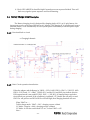
1
Product Service Manual
Service Manual for BenQ:
K61
Applicable for All Region
Version: 001
Date:2010/06/18
Notice:
- For RO to input specific “Legal Requirement” in specific NS regarding to responsibility and liability statements.
- Please check BenQ’s eSupport web site, http://esupport.benq.com, to ensure that you have the most recent version of this
manual.
First Edition (Jun., 2010)
© Copyright BenQ Corporation 2010. All Right Reserved.
-1-
Content Index
1. About This Manual..................................................................................................... 4
1.1. Trademark ............................................................................................................... 4
2. Introduction ............................................................................................................... 5
2.1. RoHS (2002/95/EC) Requirements – Applied to all countries require RoHS. ........... 5
2.2. Safety Notice ............................................................................................................ 5
2.3 .Compliance Statement ............................................................................................. 5
2.4. General Descriptions ............................................................................................... 5
2.5. Related Service Information ..................................................................................... 5
3.1 Specification ............................................................................................................. 6
3.1.1 Introduction ......................................................................................................................... 6
3.1.2 Operational Specification .................................................................................................... 6
3.1.3 Software Features .............................................................................................................. 8
3.1.3.1 General Features Summary .............................................................................................. 8
4.1. . Exploded View ..................................................................................................... 10
4.3. Packing .................................................................................................................. 13
GIFT BOX LABEL LOCATION ................................................................................... 16
5. Level 1 Cosmetic / Appearance / Alignment Service.................................................. 17
5.1 Software / Firmware Upgrade Process ................................................................................. 17
5.1.1. Put download images in SD card ......................................................................... 17
5.1.2. Start SD Download ............................................................................................. 17
6. Level 2 Circuit Board and Standard Parts Replacement........................................................ 19
6.1 System block diagram: ............................................................................................ 19
6.2.1
6.2.2
6.2.3
6.2.4
6.2.5
6.2.6
6.3
Power management circuit ............................................................................. 31
6.3.1
6.3.2
6.4
E-Paper Display Function Block .................................................................................... 35
Panel trouble shooting guide ......................................................................................... 42
WIFI ............................................................................................................... 43
6.6.1
6.6.2
6.6.3
6.6.4
6.7
Description: .................................................................................................................... 32
Function block or circuit ................................................................................................ 32
Basic Circuit operation introduction ............................................................................ 32
Debugging process .......................................................................................................... 33
PMIC ............................................................................................................................... 34
Display ............................................................................................................ 35
6.5.1
6.5.2
6.6
Basic Circuit operation introduction ............................................................................ 31
Debugging process .......................................................................................................... 31
Battery Charger circuit .................................................................................... 32
6.4.1
6.4.2
6.4.3
6.4.4
6.4.5
6.5
CPU System: Power (Page 5).......................................................................................... 20
MOBILE DRAM CONTROLLER: (Page3, 6) ............................................................... 21
System Clock: 12MHz (Page 4) ...................................................................................... 25
System Reset .................................................................................................................... 26
System RTC: 32.768KHz (Page 2, 4) .............................................................................. 28
USB 2.0 (USB Client) (Page 1, 4) ................................................................................... 29
Description: .................................................................................................................... 43
POWER ON SEQUENCE .............................................................................................. 44
Basic Circuit operation introduction ............................................................................ 44
Debugging process .......................................................................................................... 45
WWAN function (3G Modem) ....................................................................... 49
6.7.1
6.7.2
Description: .................................................................................................................... 49
Function block or circuit ................................................................................................ 50
-2-
6.7.3
6.8
Debugging process .......................................................................................................... 50
Others ............................................................................................................. 55
6.8.1
6.8.2
6.8.3
6.8.4
6.8.5
SD-card Function introduction ..................................................................................... 55
moviNAND Function introduction .............................................................................. 56
Audio Function Block .................................................................................................... 59
Touch Function Block .................................................................................................... 63
Key Function Block......................................................................................................... 64
-3-
1. About This Manual
This manual contains information about maintenance and service of BenQ products. Use this manual to
perform diagnostics tests, troubleshoot problems, and align the BenQ product.
1.1. Trademark
The following terms are trademarks of BenQ Corporation:
BenQ
Importance
Only trained service personnel who are familiar with this BenQ Product shall perform service or
maintenance to it. Before performing any maintenance or service, the engineer MUST read the “Safety
Note”.
-4-
2. Introduction
This section contains general service information, please read through carefully. It should be stored for easy
access place for quick reference.
2.1. RoHS (2002/95/EC) Requirements – Applied to all countries require RoHS.
The RoHS (Restriction of Hazardous Substance in Electrical and Electronic Equipment Directive) is a legal
requirement by EU (European Union) for the global electronics industry which sold in EU and some
counties also require this requirement. Any electrical and electronics products launched in the market after
June 2006 should meet this RoHS requirements. Products launched in the market before June 2006 are not
required to compliant with RoHS parts. If the original parts are not RoHS complaints, the replacement
parts can be non ROHS complaints, but if the original parts are RoHS compliant, the replacement parts
MUST be RoHS complaints.
If the product service or maintenance require replacing any parts, please confirming the RoHS requirement
before replace them.
2.2. Safety Notice
1.
2.
3.
4.
5.
6.
7.
8.
Make sure your working environment is dry and clean, and meets all government safety requirements.
Ensure that other persons are safe while you are servicing the product.
DO NOT perform any action that may cause a hazard to the customer or make the product unsafe.
Use proper safety devices to ensure your personal safety.
Always use approved tools and test equipment for servicing.
Never assume the product’s power is disconnected from the mains power supply. Check that it is
disconnected before opening the product’s cabinet.
Modules containing electrical components are sensitive to electrostatic discharge (ESD). Follow ESD
safety procedures while handling these parts.
Some products contain more than one battery. Do not disassemble any battery, or expose it to high
temperatures such as throwing into fire, or it may explode.
Refer to government requirements for battery recycling or disposal.
2.3 .Compliance Statement
Caution: This Optical Storage Product contains a Laser device. Refer to the product specifications and your
local Laser Safety Compliance Requirements.
2.4. General Descriptions
This Service Manual contains general information. There are 3 levels of service:
Level 1: Cosmetic / Appearance / Alignment Service
Level 2: Circuit Board or Standard Parts Replacement
Level 3: Component Repair to Circuit Boards
2.5. Related Service Information
BenQ Global Service Website: http://www.benq.com/support/
eSupport Website: http://esupport.benq.com/v2
-5-
3. Product Overview
3.1 Specification
3.1.1 Introduction
This is a code name for e-Book reader device which is targeted at the specific book reading purpose.
It adopts e-paper panel as the main display to reach low power consumption and get better feeling
when reading. The embedded QReader can support several popular e-book formats, like DPF,
ePub, Html and several image formats, like JPEG, PNG and BMP. This e-book device is capable to
communicate to a Wifi Router or 3G Station directly. User can easily download the content from
Internet or operator service platform. The User Interface uses AUO capacitive in-cell touch and
enables the handwriting capability. User can add a bookmark or make a note easily when reading.
The whole system adopts mobile technology and materials to reach lowest power consumption
and slim industrial design.
Item
Screen Size
Display Resolution
Overall Dimension
General Information Gray Level
Weight
Touch Panel
Touch Scan Rate
Reflectance
Optical Specification
Contrast Ratio
Unit
inch
dot
mm
-g
Specification
6(Diagonal)
800(H)x600(V)
192(H)x130(V)x99(T)
16
299
Hz
R
CR
Capacitive Type
Up to 85 Hz
30
6:1
Note
A060SE02 V2
90%
transmitting rate
3.1.2 Operational Specification
3.1.2.1 Feature List-Electrical
Category Item
Specification
SOC
Memory
Electrical Connector
Audio
Sensors
Battery
S3C2416 ARM 9 400MHz
Mobile DDR
SLC NAND Flash
MLC NAND Flash
USB Host
USB Device
SD slot
Earphone jack
Amplifier
Speaker
Tilt sensor
G-sensor
Charger
128 MB
NA
2 GB
USB 1.1 Host
USB 2.0 Device
Yes
Yes
n/a
Single
n/a
n/a
Yes
-6-
Remark
65nm process; 330-FBGA,
0.65mm pitch
16-bit data bus I/F
Samsung Movi-Nand
A type
Micro USB-B type
Build-in battery
1480 mAh
Standby mode
15 days
lifecycle
Reading mode Page Above 7500 Pages
LEDs
Charging
Menu
Yes
Page up*2
Yes
Page down*2
Yes
Keys
Back
Yes
System wake-up /
Tact Switch
Off
TD HSDPA/
Connectivity TDS-CDMA
TDSCDMA/GSM/GPRS/EDGE
-7-
LeadCore 5730+
3.1.3
Software Features
3.1.3.1 General Features Summary
Item
Description
Specification
OS
Description
V 2.6.21
Middleware
Qt
V4.5.1
PDF (Adobe)
Yes
Adobe Mobile Reader 9
HTML
Yes
Webkit
TXT
Yes
Qisda
EPUB
Yes
Adobe Mobile Reader 9
Meb
Yes
JPEG
*.jpg
PNG
*.png
BMP
*.bmp
MP3
Yes (audio book)
Audio Format
AAC
n/a
e-Book DRM
ePub, PDF
Adobe CS4
Font size adjustment
Yes, 3 font sizes
Book list
Recent (download/import)
books, Unread books, Books
by title, Books by Author,
Books by Date, My favorite
books
Bookmarks
Add, Delete, List, View
Note Tool (Footnote)
Yes
Software keyboard
English, Number, Symbols
Audio book (TTS)
n/a
File management
Yes
Background music
Yes
Book Search
Yes
Keyword Search
Yes
Favorite List
Yes
Photo information
Yes
Next / Prev.
Yes
Rotate
Yes
File management
Yes
Music information
Yes
File Sorting
File Name
Document format
Image Format
Reader Mode
Picture Mode
Audio Mode
-8-
Remark
(Small, Medium, Large)
Settings
Next/ Prev.
Yes
Repeat/Random
Yes
Stop/Pause/Play
Yes
Volume control
Mute/1/2/3/4/5
Low battery warning
Yes
3.45V for warning message
3.3V for system booting
Power Management
Setting
Yes
When enabling PM, device will
enter sleeping mode after 30
seconds .
FW upgrade
Yes
SD Card Mode
Device information
0. Linux version
1.File system version
2.Kenerl Version
3.Boot code version
4.Waveform(LUT) version
5.T-CON firmware version
6.Temperature
7.DRAM size
8Free Flash Memory Size
-9-
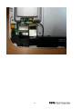
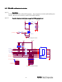
4. Disassembly /Assembly
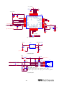
4.1. . Exploded View
- 10 -
4.2. Disassembly /Assembly
1
Turn off power and remove attachments. (shown
in following figure)
(1) Antenna cover (2) Screw x 3
2
Screw off screw from top of rear case
3
Remove case rear
4
Separate antenna holder: Disconnect
(1) Mylar
(2)Switch wire (from 3G module)
(3)SPK connector
- 11 -
5
6
7
8
Separate metal sheet :
(1) remove screw( x10)
(2) disconnect Batt. connector
Separate main board from front case:
(1)Disconnect key FFC
(2)Disconnect Wifi antenna wire
(3)Disconnect Panel FFC
(4)Disconnect Touch FFC
(5)Remove Cu foil (x2)
Take page keys out from front case
Separate function key and EPD from housing:
(1) unscrew × 3
(2) remove key PCB
(3) take out keypad
(4) remove EPD
- 12 -
4.3. Packing
DEVICE LABEL LOCATION
WARRANTY SEAL
WATER DETECTION LABEL
SPEC LABEL
NETWORK PERMISSION LABEL
- 13 -
GIFT BOX PACKING DESCRIPTION
(1)將 S/N LABEL 貼在保卡上
(1) 再依序將保卡、QSG、說明書(封面朝上)、皮套(印有 G3 logo 面朝上)擺放於彩盒底部
(2) 將內襯放入盒內,再將 SD 卡、充電器及 USB CABLE 如下圖所示,放入相應位置
SD 卡
充電器
USB CABLE
- 14 -
(3) 將耳機放在 SD 卡上
耳機
(4) 最後將機器置於最上層,並蓋上透明內襯蓋
- 15 -
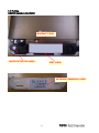
GIFT BOX LABEL LOCATION
GIFT BOX LABE
請沿標籤定位線黏貼
CARTON LABEL LOCATION
CTN LABEL 黏貼處
- 16 -
5. Level 1 Cosmetic / Appearance / Alignment Service
5.1 Software / Firmware Upgrade Process
本文件描述如何透過 SD 卡將 uboot, kernel (zImage),root file system 更新到 e-book 上.
5.1.1. Put download images in SD card
直接在 Windows 下, 將所需要更新的 images 依照下面規定的目錄結構放入 SD card. 附檔名
請固定小寫(bin).
Firmware 包含
u-boot and zImage.
rootfs.ext3.00 and rootfs.ext3.01
Directory layout for download images (目錄名稱要小寫)
/qdutil/
upfw/
u-boot.bin
zImage
rootfs.ext3.00
rootfs.ext3.01
5.1.2. Start SD Download
Step 1: 插入準備好的 SD-Card
Step 2: e-book 進入系統設置-高級設置-/軟件升級-由存儲卡上進行升級
在進行軟件升級時,電池電力需有 2 格,
如已彈出提示電力不足時,請回到首頁,插入 USB cable 後, 重新進入系統設置,選 取由存儲
卡上進行升級
另有強制升級的方式:在開機狀態中, 同時按住 e-book page up and page down key, 再按一
下 reset key
Step 3: 當看到”軟件更新中的畫面” 即已啟動 Firmware Upgrade
Step 4: 當方塊條全黑表示 download 完成
- 17 -
Step 5: Firmware Upgrade 完成後,e-book 自動開機,進入時間設置,,設定時間後,畫面回到首頁
開機中
畫面回到首頁
更新時間說明: 約在 4 分鐘內完成一次更新操作, 其中, uboot.bin and zImage 約花 10 秒,
rootfs.ext3.00 and rootfs.ext3.01 約花 230 秒
- 18 -
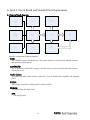
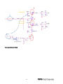
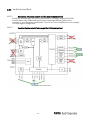
6. Level 2 Circuit Board and Standard Parts Replacement
6.1 System block diagram:
Fig. 2
Some key components of above diagram:
DDR:
The 128MB low power DDR memory is for system software to execution the eReader software
and operating system kernel.
moviNAND:
The 2GB internal moviNAND storage is used for store the system software and books content
during power off.
Audio Codec:
The features of audio codec include: Audio DAC, Class-D Audio Power Amplifier and Earphone
driver.
TCON:
The timing controller for display panel is made by FPGA.
SDRAM:
The frame buffer for display data.
EPD:
The display panel.
- 19 -
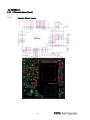
6.2 SMDK2416
6.2.1 CPU System: Power (Page 5)
6.2.1.1
Function Circuit/ Layout
- 20 -
6.2.1.2
6.2.1.3
Recommended Operating Conditions
Circuit Operation:
1. Adaptor in, Power ON device
2.工作電壓, System Clock 起來
6.2.1.4
Debugging Process
6.2.1.4.1 Possible failure symptoms
系統開不了機、螢幕不會亮、連接周邊 IO 介面無 Function.
6.2.1.4.2 Debugging steps
1. 目視相關元件是否正常
2. Check 2416 power rail
3.有問題再去作分析問題所在!
6.2.2 MOBILE DRAM CONTROLLER: (Page3, 6)
6.2.2.1
Description
The S3C2416 Mobile DRAM Controller supports three kinds of memory interface - (Mobile)
SDRAM and mobile DDR and DDR2. Mobile DRAM controller provides 2 chip select signals (2
memory banks), these are used for up to 2 (mobile) SDRAM banks or 2 mobile DDR banks or 2 DDR2
banks. Mobile DRAM controller can’t support 3 kinds of memory interface simultaneous, for example
one bank for (mobile) SDRAM and one bank for mobile DDR.
- 21 -
Mobile DRAM controller has the following features:
• Support little endian
• Mobile DDR SDRAM and (Mobile) SDRAM
−Supports 32-bit for SDRAM and 16-bit data bus interface for mDDR and DDR2.
−Address space: up to 128Mbyte
−Supports 2 banks: 2-nCS (chip selection)
−16-bit Refresh Timer
−Self Refresh Mode support (controlled by power management)
−Programmable CAS Latency
−Provide Write buffer: 8-word size
−Provide pre-charge and active power down mode
−Provide power save mode
−Support extended MRS for mobile DRAM)
♦ DS, TSCR, PASR
6.2.2.2
Function Circuit and Layout
- 22 -
Layout:
6.2.2.3
Circuit Operation:
1. Adaptor in, Power ON device
2. DDR Interface 工作電壓和 Clock 起來
3. DRAM Timing Diagram
- 23 -
6.2.2.4
Debugging Process
6.2.2.4.1 Possible failure symptoms
6.2.2.4.2
系統開不了機、螢幕不會亮、連接周邊 IO 介面無 Function.
Debugging steps
1. 目視相關元件是否正常
2. Check DDR power: VDD_18M/ VDD_DDR => 1.8V
3. Check 2416 DDR power: VDD_18M/ VDD_SMOP => 1.8V
4. Check DDR Clock: SCLK, nSCLK
5. Check DDR IO block 有問題再去作分析問題所在?
- 24 -
6.2.3 System Clock: 12MHz (Page 4)
6.2.3.1
Function Circuit and Layout
C403
20P G
XTIPLL
R405
1M J
XTOPLL
C404
1
Y 402
2
4
3
12MHZ
20P G
6.2.3.2
Circuit Operation:
1. Adaptor in
2. Clock 起來
6.2.3.3
Debugging Process
6.2.3.3.1 Possible failure symptoms
系統開不了機、螢幕不會亮、連接周邊 IO 介面無 Function.
6.2.3.3.2
Debugging steps
1. 目視 Clock 相關元件是否正常
2. Clock: XTIPLL, XTOPLL =>12MHz
3.有問題再去作分析問題所在!
- 25 -
6.2.4 System Reset
6.2.4.1
Function Circuit/ Layout (Page 1, 3)
6.2.4.2
Circuit Operation:
1. Adaptor in, Power ON device
2. Press Reset Button, system reset (Re-start)
6.2.4.3
Debugging Process
6.2.4.3.1 Possible failure symptoms
系統無法 Reset
- 26 -
6.2.4.3.2
Debugging steps
1. 目視 Reset 相關元件是否正常
2. Check nRESET 訊號是否正常
3. 有問題再去作分析問題所在!
- 27 -
6.2.5 System RTC: 32.768KHz (Page 2, 4)
6.2.5.1
6.2.5.2
Finction Circuit/ Layout
Circuit Operation:
1. With battery
2. VDD_RTC 工作電壓起來
3. RTC Clock 起來
6.2.5.3
Debugging Process
6.2.5.3.1 Possible failure symptoms
RTC fail
6.2.5.3.2 Debugging steps
1. 目視 RTC 相關元件是否正常
2. Check RTC LDO U202, check VDD_RTC=>3V
3. Check RTC clock => 32.768KHz
4. 有問題再去作分析問題所在!
- 28 -
6.2.6 USB 2.0 (USB Client) (Page 1, 4)
6.2.6.1
Function circuit and layout
. .
1
VBUS
D107
2
J101
VUSB_5V
DM
DP
ID
GND
1
C122
C114
10U K
10U K
15V 150PF
L102
Z220
2
1
DM_UDEV {4}
3
4
3
5
DLW21HN900SQ2LGP
R105
VAR105
10V_1.1P
VAR106
10V_1.1P
Mini _USB
Mini-USB
4
33 J
DP_UDEV {4}
C_MODE
{4}
R139
1
D108
G1
G2
G3
G4
100K J
2
15V 150PF . .
GND1
GND2
GND3
GND4
TR101
2
C121
47U 6.3V
VDD_D
USB Internal Clock (48MHz)
VDD_USB33
C407
L402
Z300
4
L403
Z300
1
Y 401
VDD
OUT
Vcont GND
3
R417
120 J
XO_UDEV
2
C408
48MHZ
NC_18P 50V
0.1U K
- 29 -
6.2.6.2
Circuit Operation:
1. Adaptor IN, Device Power ON
2. VDD_USB_33 工作電壓起來, USB Clock: XO_UDEV 起來
3. Plug in USB cable, connect device to PC, => VBUS=5V
4. 畫面點選起動 U 盤模式
5. Check D+/D- 是否有訊號
6.2.6.3
Debugging Process
6.2.6.3.1 Possible failure symptoms
USB Fail
6.2.6.3.2 Debugging steps
1. 目視 USB 相關元件是否正常
2. Check VDD_USB_33=>3.3V
3. Check USB Clock: XO_UDEV => 32.768KHz
4. Plug in USB cable, connect device to PC, => VBUS=5V
5. Check D+/D- 是否有訊號
6. 有問題再去作分析問題所在!
- 30 -
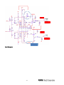
6.3 Power management circuitBasic Circuit operation introduction
Power on & power sequence
In Battery mode, when pressed SW101, will enable VDD_D & VDD_18M,then PMIC has
3.3V & 1.8V output and SSC2416 power on, then going on following boot sequence.
6.3.2 Debugging process
6.3.2.1
Possible failure symptoms
1. Large leakage current
2. Cannot boot, debug board did not run.
6.3.2.2
Debugging steps
1. Plug-in Battery, check leakage current, it should under 0.1 mA .
2. a. Power on system, check U101 power, check VBAT power, if no VBAT, check
U102
b. Check U201 power, check VDD_D(3.3V/Pin 8) , VDD_18M (1.8V/Pin 25) , VDD_ARM
(1.29V/Pin 1), VDD_ARM2 (1.29V/Pin 1),if no power found ,check
U201,L201,L202,L203 .
c. Check power on sequence, check XTIPLL CLK, if no clock found, replace Y402
- 31 -
d. Check CPU nRESET,it should be high if normal power on sequence finished. Then roll
back every signal at power sequence and check trimming.
6.4 Battery Charger circuitDescription:
The Battery charging circuit is designed for charging single cell Li+ or Li-poly battery, the
input power source can be from USB host or AC Adapter. The charging IC is include power source
selection feature, it can automatically to select system power from battery or external power input
during charging.
6.4.2 Function block or circuit
a. Charging Schematic
6.4.3 Basic Circuit operation introduction
When the adapter and the Battery in, VBUS > UVLO AND VBUS> VBAT + VIN(DT) AND
VBUS< VOVP and -1˚C <VBAT_TEMP<50˚C and the EN1 and EN2 pins indicate that the
USB suspend mode is not enabled [(EN1, EN2) ≠ (HI, HI)] ,all internal timers and other
circuit blocks are activated, If the condition is confirmed , CE_Enable Pin will pull Low and
CHG Pin will pull low and PGOOD Pin will Pull High ,then charging function will start.
When VBAT in…..
Trickle charge mode : VBAT < 2.8V , charging current =89mA
CC Mode : Capacity < 90% , charging current =890mA
CV Mode : it will auto switch from CC to CV when VBAT =4.2V
Note :
- 32 -
(1) UVLO: 4.5V
(2) VIN(DT) : 55~130mV
(3) VOVP : 6.4~6.6V
6.4.4 Debugging process
6.4.4.1
Possible failure symptoms
Use the power supply (5V) to supply the Adapter .
If ……
1. Power supply current is under 150 mA (see the 2.3.4.2)
2. Power supply current is over 1A (see the 2.3.4.3)
3. LCD no display
6.4.4.2
Debugging steps
Probable Cause
(a)
Check U101 signal
Verification and Remedy
1. check the below signal :
a. 5V<IN( Pin 13 ) <6.8V
b. OUT1 and OUT2 (Pin 10 and Pin11) > 4.2V
2. If it is still no output, proceed to b.
1. Visually inspect the U101 . If the pins of the U101 and contact NG,
(b)
Components NG
re-solder the pins.
2. Visually inspect the U102, If any component is not contacted well,
replace the component. If it is necessary, change a new one.
6.4.4.3
Debugging steps
Probable Cause
(a)
Check U101 signal
Verification and Remedy
1. check the below signal :
a. IN( Pin 13 ) is short with GND
b. OUT1 and OUT2 (Pin 10 and Pin11) is short with GND
c. Take off U201,than check a and b step again
2. If it is short with GND, proceed to b.
3. If it is good, proceed to c
1
(b)
Components NG
Visually inspect the U101 . If the pins of the U101 and contact NG,
re-solder the pins.
2
Visually inspect the U102, If any component is not contacted well,
replace the component. If it is necessary, change a new one.
(a)
Check U201 signal
1.
check the below signal
a. VDCDC1 (Pin 8),VDCDC2 (Pin 25),VDCDC3 (Pin 1)
- 33 -
(d)
Components NG
2.
is short with GND
If it is still short with GND, proceed to d
1
Visually inspect the U201 . If the pins of the U201 and contact NG,
re-solder the pins.
2
Visually inspect the U201,L201,L202,L203, If any component is not
contacted well, replace the component. If it is necessary, change a
new one.
6.4.5 PMIC
6.4.5.1
Description:
6.4.5.1.1 Function purpose
Power providing for the core voltage ,peripheral, I/O and memory .
6.4.5.1.2 Major components list
1. PMIC(U201)
2.CHIP PWR IND 2.2U(L201,L202,L203)
6.4.5.2
6.4.5.2.1
Function block or circuit
PMIC circuit
- 34 -
6.4.5.3
Basic Circuit operation introduction
1. When the adapter in or Battery in , press Power on key, U101 will provide a regulated
output VBAT to PMIC, PMIC DCDC1_EN & DCDC2_EN Pin will be enabled by
VBAT, then PMIC will provide regulated output VDD_D and VDD_18M
2. After VDD_D output is stable, PMIC EN_alive Pin will be enabled by VDD_D, then
PMIC will provide a regulated output VDD_ALIVE (1.2V)
3. After VDD_D and VDD_18M output voltage are stable,,S3C2416 will send PWR_EN
to DCDC3_EN,then PMIC will provide a regulated output VDD_ARM 1/ 2 (1.3V)
6.4.5.4
Debugging process
6.4.5.4.1 Possible failure symptoms
Use the power supply (5V) to supply the Adapter .
If ……
1. Power supply current is under 150 mA
2. LCD no display
3. Can’t boot
6.4.5.4.2 Debugging steps
Probable Cause
Verification and Remedy
3
4
(a)
Check U201 signal
(b)
Components NG
5
6
7
8
check the below signal
VCC (Pin 29),VINDCDC1(Pin5), VINDCDC1(Pin28)
VINDCDC2(Pin4),DCDC1_EN(Pin20),
DCDC2_EN(Pin19), > 4.2V
VDCDC1 (Pin 8)>3.3V
VDCDC2 (Pin 25)>1.8V
DCDC3_EN (Pin 18) > 3.3V
VDCDC3 (Pin 1)>1.29V
9
If it is still no output, proceed to d
1
Visually inspect the U201. If the pins of the U201 contact NG, resolder the pins.
2
Visually inspect the L201, L202, L203. If any component is not
contacted well, replace the component. If it is necessary, change a
new one.
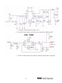
6.5 Display E-Paper Display Function Block
(CPU TCON Panel)
- 35 -
TCON FPGA
TCON FPGA is an EPD controller for E-Book application, the outputs have 2 bit output per
pixel. The timing controller provides control signals for the source driver and gate drivers.
AUO-K1900(TCON) provides a high performance, low cost solution for Sipix EPDs
(Electronic Paper Display), it also includes external mobile SDRAM controller, built in temperature
sensor. Multi-region and concurrent display updates resulting in high responsive screen changes are
also embedded in special timing controller for these applications.
FPGA Flash
Store pre-programmed FPGA code for TCON function.
LUT Flash
Store source/gate driving waveform Look-Up-Table for different temperature and different
display mode
- 36 -
Thermal Sensor
Detect E-Paper environmrnt temperature. (目的是偵測 EPD 溫度,調整 LUT 參數)
SDRAM
TCON display buffer and working space.
E-Paper Display Power Distribution
FPGA Power
- 37 -
Panel power Source & VCOM
- 38 -
Panel Gate power
- 39 -
Panel power sequence control
- 40 -
Disable ESD reset circuit for panel
Set RC20 RC22 RC21 RC23 LC6 CC18 QC10 QC12 QC09 QC11 to NC
- 41 -
Panel power sequence control
6.5.2 Panel trouble shooting guide
Important!!! : Before removing panel, Please disconnect any power source ( Battery and USB) first and
wait for 30 seconds.
Symptom
1.No display
Probable Cause
Device hangs.
Verification and Remedy
1. Connect debug board, check system is alive or not.
2. If device hangs, check CPU and other relate circuit
first.
Panel defect.
1.Remove panel, connect USB to prevent device go into
sleep mode, power on device, check panel power
V, +11.5V, -18.5V
2. If power OK, disconnect power and replace panel, and
check again
TCON fail
1. Check TCON power source, 3.3V, 1.8V and 1.2V, if
power fail, check relate circuit.
2. Check TCON oscillator ,should be 33M
3. Check SDRAM and TCON Flash and LUT Flash
relate circuit.
4. If all above looks OK, replace TCON flash and LUT
flash with FW inside, check again.
5. If 4 fail, replace SDRAM and check again.
6. If 5 fail, replace TCON.
- 42 -
2. Has display, but
abnormal
Panel power fail
1. Check schematic P.12 VCC1 and VDD_P,
if fail, check QC11~ QC14, and
TCON_PWREN signal.
2. Check panel power.
V, +11.5V, 18.5V, If fail, check P.18 page components.
3. Check VDDX8 & NVDDX8 ( need to
connect panel) if no power (
20V)
check QG01, QG02, ZDG1, ZDG2, DG01,
DG2, DG03 and P.15 relate circuit.
Panel defect.
1.Remove panel, connect USB to prevent device go into
sleep mode, power on device, check panel power
V, +11.5V, -18.5V
2. If power OK, disconnect power and replace panel, and
check again
1. Check TCON power source, 3.3V, 1.8V and 1.2V, if
power fail, check relate circuit.
TCON Fail
2. Check TCON oscillator ,should be 33M
3. Check SDRAM and TCON Flash and LUT Flash
relate circuit.
4. If all above looks OK, replace TCON flash and LUT
flash with FW inside, check again.
5. If 4 fail, replace SDRAM and check again.
6. If 5 fail, replace TCON.
6.6 WIFIDescription:
Wifi :
High speed for wireless LAN connection: IEEE802.11b/g up to 54Mbps data rate by
incorporating Direct Sequence Spread Spectrum (DSSS) and OFDM data modulation.
Main Components:
Main module is USI WM-G-MT03 and MTK MT5921 inside, wifi RF trace is controlled
as 50 ohm, wifi antenna is PIFA type and paste on board.
WM-G-MT03 Block Diagram:
- 43 -
6.6.2 POWER ON SEQUENCE
6.6.3 Basic Circuit operation introduction
Step 1 : System supply 3.3V and 1.8V power, then Enable “WIFI_EN1V8_1”and
“WIFI_EN3V3_1” to switch on it.
Step 2 : When power in Wifi module, system will issue reset signal “EXT_N_RST” to
module.
Step 3 : System will drive Wifi-BT to initial its Function.
- 44 -
Step 4 : Form OS, wifi will search AP after you tune on wifi function.
6.6.4 Debugging process
6.6.4.1
possible failure symptoms
1. NO response after tune on Wifi from OS
2. Wireless connection distance is not enough.
6.6.4.2
Debugging steps
Wifi PIFA antenna
- 45 -
Feed point
GND point
Paste area
Cable connector
Wifi module
- 46 -
Wifi matching circuit
Wifi module
Failure symptom
A. NO response after tune on Wifi from OS
1. Check all parts of wifi block are correct parts and soldering well.
2. Check UA03 pin3 logic level is “H” and pin1 is 1.8V
3. Check UA03 pin4 logic level is “H” and pin6 is 3.3V
4. After power in, check Net “EXT_N_RST” change logic level from “L” to “H”.
5. Check SPI interface signal (compare with normal one).
6. Check UA02 pin43 is 32KHz clock
7. When device is searching AP, check UA02 pin5 power delivery is controlled by
UA02 pin3. If pin3 level is “H”, pin5 voltage is VBATT.
B. Wireless connection distance is not enough
1. Check wifi antenna feed point and GND point soldering is well.
2. Check wifi antenna pasted area is well (confirm antenna GND point and PCBA
GND is well connection).
3. Check wifi matching circuit value(CA15 and CA17).
- 47 -
4. Check cable connector.
5. change a new wifi antenna.
- 48 -
6.7 WWAN function (3G Modem)Description:
There are 2 PCI Express Mini Card Module option as below,
1. Leadcore : Support TD-SCDMA, E-GSM, DCS1800 and PCS1900. Power
supply 3.2 ~4.2V.
2. ZTE : Support WCDMA, HSPDA, E-GSM, DCS1800 and PCS1900, power
supply 3.3~3.6V
Different power supply range, we design different power options for these 3G modem.
For Leadcore
For ZTE
Main Components:
1.
3G module (Leadcore LC5730 or ZTE MF200)
2.
2G/3G SIM card
3.
Power supply to 3G module
4.
Antenna
- 49 -
6.7.2 Function block or circuit
Single Antenna
Supply power
Power
Ground
Connector
3G Module
Control Interface
USB/USIM Interface
USIM
Main Board
6.7.3 Debugging process
6.7.3.1
Possible failure symptoms
Before you want to net web book store by 3G, confirm the correct SIM card and
back cover assembly well. 3G won’t enable if back cover don’t be assembly well.
- 50 -
1. Can’t net to web book store by 3G from OS
2. Wireless connection quality is not stable
6.7.3.2
debugging steps
Failure symptom
A. Can’t net to web book store by 3G from OS
a. Power trace:
Leadcore LC5730:
1. Check RL31 mounted and impedance less than 0.04 ohm.
2. Check below part mounted, soldering well and NET “3G_EN” is high
level
3G RF cable to PIFA antenna
H10 module
Connector
3. Confirm +3P3Vaux power level is the same with Li-BAT (3.4~4.2V)
ZTE MF200:
1. Check RL29 mounted and impedance less than 0.04 ohm.
2. Check below part mounted (inside shielding case), soldering well and
NET “3G_EN” is high level.
- 51 -
3. Confirm +3P3Vaux power is about 3.45V
b. Check SIM card connector and relative part mounted and soldering well.
c. Check PCI Express Mini Card connector soldering and interface component.
- 52 -
d. If you find system reset at enable 3G module or 3G fail at re-enable it quickly,
you need check soft-start key part CL4 or CL21, and discharge parts RL18
and QL2.
B. Wireless connection quality is not stable
1.
2.
3.
4.
5.
Check RF cable and connector well join.
Check conductive test.
Check antenna version (mark on antenna)
Swap 3G module and single antenna to confirm failure in which one.
Change a new one for failure part.
- 53 -
- 54 -
6.8 OthersSD-card Function introduction
6.8.1.1
Description:
S3C2416 read/writes SD card by SDIO interface。The components includes Q801/Q802(power
switch) , J801(SD-card connecter), and S3C2416 SDIO interface.
6.8.1.2
Function block or circuit ( also can put the PCB layout picture)
VDD_D
VDD_SSD
Q801
S
D
0J
SI2301CDS-T1-GE3
G
R801
R805
C801 C802
1U K 10U K
D
100K J
R806
{4} PWREN_SD
Q802
G
100K J
S
C803
2N7002K-T1-E3
0.01U K
(1) SD card power switch
5
6
7
8
10K
SD0_CMD1
SD0_DAT3
SD0_CMD
SD0_CLK1
SD0_CLK
SD0_D0
SD0_DAT0
SD0_DAT1
SD0_DAT2
SD0_nCD_
R802
R803
VDD_SSD
NC_4.7K J
RN801
R804
4
3
2
1
10K J
100K J
VDD_D
J801
R813
R814
0J
0J
SD0_DAT3_1
SD0_CMD_1
1
2
R815
0J
SD0_CLK_1
4
5
R816
R817
R818
0J
0J
0J
SD0_DAT0_1
SD0_DAT1_1
SD0_DAT2_1
7
8
9
10
{4} SD0_nCD
12
SD0_WP
.
.
.
.
.
.
.
.
.
.
.
.
.
.
.
.
.
.
1
1
D808
1
D807
1
D805
1
D804
1
D803
1
D802
1
D801
1
D806
D809
{3} SD0_WP
150PF
150PF
150PF
150PF
150PF
150PF
150PF
150PF
150PF
SD0_DAT0
SD0_DAT1
SD0_DAT2
SD0_DAT3
SD0_CMD
SD0_CLK
NC_15V
NC_15V
NC_15V
NC_15V
NC_15V
NC_15V
15V
NC_15V
NC_15V
{4} SD0_CMD
{4} SD0_CLK
2
2
2
2
2
2
2
2
2
{4} SD0_DAT[3:0]
(2) S3C2416 SDIO interface
- 55 -
CD/DAT3
CMD
SH1
SH2
13
G1
VDD
CLK
DAT0
DAT1
DAT2
VSS2
VSS1
6
3
CD Pin
WP Pin
CD/WP(GND)
PSDBT5 -09GLBS1N14N0
11
(3) S3C2416 SDIO interface
6.8.1.3
6.8.1.4
Basic Circuit operation introduction
1.When SD-card inserted, SD0_WP 3.3V -> 0V, and generate a interruption to Host
2.Host pull high PWREN_SD, and turn on VDD_SSD
3.Host start to send SD0_CLK and SD0_CMD to SD-card
4.SD-card and Host deliver data by SD0_DAT0 ~ SD0_DAT3
Debugging processpossible failure symptoms
As Host can’t configure SD-card or Host can’t read/write SD-card data
6.8.1.4.2 debugging steps
1. U301 and J801 SMT well? If not, need to repair it.
2. When SD-card inserted, does SD0-WP pull low? If not, check WP pin components.
3. Check PWREN_SD is high ; VDD_SSD is 3.3V? If not, check SD power components.
4. Check SD0_CLK is normal(24MHz)? If not, check SD0_CLK components.
5. Check SD0_CMD is normal? If not, check SD0_CMD components.
6. Check SD0_DAT0~3 are normal? If not, check SD0_ DAT0~3 components
6.8.2 moviNAND Function introduction
6.8.2.1
Description:
Homer use SAMSUNG moviNAND which is a embedded MMC solution. moviNAND operation is
identical to a MMC card and therefore is a simple read and write to memory using MMC protocol
v4.3 which is a industry standard. moviNAND consists of NAND flash and a MMC controller.
6.8.2.2
Function block or circuit ( also can put the PCB layout picture)
(1)moviNAND block diagram
- 56 -
8
7
6
5
VDD_D
Movi NAND (2GB)
U801A
R810
1
2
3
4
RN802
10K
{4} SD1_DAT[3:0]
10K J
DT4
DT5
DT6
DT7
H3
H4
H5
J2
J3
J4
J5
J8
SD1_CMD
SD1_CLK
W5
W6
SD1_DAT0
SD1_DAT1
SD1_DAT2
SD1_DAT3
{4} SD1_CMD
{4}
SD1_CLK
L4
DATA0
DATA1
DATA2
DATA3
DATA4
DATA5
DATA6
DATA7
CMD
CLK
A1 index
VDDI
VDD
VDD
VDD
VDD
VDD
VDDF
VDDF
VDDF
VDDF
VSS
VSS
VSS
VSS
VSS
VSS
VSS
VSS
VSS
K2 C805
K6
W4
Y4
AA3
AA5
VDD_D
0.1U K
R807
C807 C808
1U K
0.1U K
M6
N5
T10
U9
VDD_D
R808
C804 C806
K4
M7
P5
R10
U8
Y2
Y5
AA4
AA6
1U K
0.1U K
AH11
AH9
AH6
AH4
AG13
AG2
AE14
AE1
AA14
AA13
AA12
AA11
AA10
AA9
AA8
AA7
AA2
AA1
Y14
Y13
Y12
Y11
Y10
Y9
Y8
Y7
Y6
Y3
Y1
W14
W13
W12
W11
W10
KLM2G1DEDD-B101
NC
NC
NC
NC
NC
NC
NC
NC
NC
NC
NC
NC
NC
NC
NC
NC
NC
NC
NC
NC
NC
NC
NC
NC
NC
NC
NC
NC
NC
NC
NC
NC
NC
NC
U801B
NC
NC
NC
NC
NC
NC
NC
NC
NC
NC
NC
NC
NC
NC
NC
NC
NC
NC
NC
NC
NC
NC
NC
NC
NC
NC
NC
NC
NC
NC
NC
NC
NC
NC
NC
W9
W8
W7
W3
W2
W1
V14
V13
V12
V3
V2
V1
U14
U13
U12
U10
U7
U6
U5
U3
U2
U1
T14
T13
T12
T5
T3
T2
T1
R14
R13
R12
R5
R3
R2
NC
NC
NC
NC
NC
NC
NC
NC
NC
NC
NC
NC
NC
NC
NC
NC
NC
NC
NC
NC
NC
NC
NC
NC
NC
NC
NC
NC
NC
NC
NC
NC
NC
NC
NC
NC
NC
NC
NC
NC
NC
NC
NC
NC
NC
NC
NC
NC
NC
NC
NC
NC
NC
NC
NC
NC
NC
NC
NC
NC
NC
NC
NC
NC
NC
NC
NC
NC
NC
NC
K11
K12
K13
K14
L1
L2
L3
L12
L13
L14
M1
M2
M3
M5
M8
M9
M10
M12
M13
M14
N1
N2
N3
N10
N12
N13
N14
P1
P2
P3
P10
P12
P13
P14
R1
A4
A6
A9
A11
B2
B13
D1
D14
H1
H2
H6
H7
H8
H9
H10
H11
H12
H13
H14
J1
J7
J8
J9
J10
J11
J12
J13
J14
K1
K3
K5
K7
K8
K9
K10
(2)moviNAND IC
- 57 -
0J
KLM2G1DEDD-B101
0J
VDD_NAND
VDD_D
R812
0J
Q803
S
D
SI2301CDS-T1-GE3
G
R809
D
100K J
R811
100K J
G
C809
S
{4} PWREN_NAND
Q804
2N7002K-T1-E3
0.01U K
(3)moviNAND power switch
2.9.1.3 Basic Circuit operation introduction
1.Host pull up PWREN_NAND to turn on VDD_NAND
2.Host start to send clock(SD1_CLK) and command(SD1_CMD) to moviNAND
3.Host and moviNAND deliver data by SD1_DAT0 ~ SD1_DAT3
6.8.2.3
Debugging process
6.8.2.3.1 possible failure symptoms
As Host can’t read/write moviNAND
6.8.2.3.2 debugging steps
1. U801 SMT well? If not, need to repair it.
2. Check PWREN_NAND is high; VDD_NAND is 3.3V?
If not, check NAND power components.
3. Check SD1_CLK is normal(24MHz)? If not, check SD1_CLK components.
4. Check SD1_CMD and SD1_ DAT0~3 is normal?
If not, check SD1_CMD and SD1_ DAT0~3 components.
- 58 -
6.8.3 Audio Function Block
6.8.3.1
Description: (Function purpose and the major components list)
Homer has an audio codec ALC5624 on main PCBA. It is a highly-integrated I2S/PCM
interface audio codec. Differential input/output connections efficiently reduce noise
interference, providing better sound quality. Class-AB or Class-D amplifiers are easily swapped
via simple register configuration.
6.8.3.2
Function block or circuit ( also can put the PCB layout picture)
(1) Audio function block
- 59 -
AVCC_CODEC
AGND
DVCC_CODEC
48
47
46
45
44
43
42
41
40
39
38
37
C728
0.1U K
AGND
GPI 05
GPI 04
GPI 03
GPIO2/IRQOUT
GPIO1
HPVDD
AGND2
HP_OUT_R
HPGND
HP_OUT_L
SPKVDD
SPK_OUT_RN
DVDD1
MCLK
EXTCLK
DGND1
SDAC
BCLK
DGND2
SADC
DVDD2
SDALRCK
RESET#
SADLRCK
ALC5624-GRT
{3} AUDIO_RESETn
SPK_OUT_R
SPK_OUT_L
SPKGND
SPK_OUT_LN
MONO_OUTN
MONO_OUT
MIC2N
MIC2P
MICBIAS
VREF
AGND1
AVDD1
ThermalPad
SCL
SDA
NC
MICBIAS2
AVDD2
AGND3
PHONEP
PHONEN
MIC1P
MICIN
LINE_IN_L
LINE_OM_R
1
2
3
4
5
I2S0_SDO_PCM0_SDO_AC_SDO
6
IIS_BCLK
7
8
9
10
I2S0_LRCK_PCM0_FSYNC_AC_nRESET R708
0J
11
10K J AUDIO_RESETn
DVDD_AUIO R716
12
C729
22P J
IIS_MCLK1
U701
36
35
34
33
32
31
30
29
28
27
26
25
G1
LOUTP_L
LOUTN_L
AGND
VREF_A
AVCC_CODEC
AGND
13
14
15
16
17
18
19
20
21
22
23
24
C727
0.1U K
HP_OUT_L
SPKVDD
HP_OUT_R
C724
0.1U K
C711
4.7U K
C726
0.1U K
C725
0.1U K
AGND
AGND
AGND
AVCC_CODEC
R714
R702
SDA_AUDIO
SCL_AUDIO
10
10
(2) Audio Codec
VDD_D
DVDD_AUIO AUD
U702
3
4
C708
10U K
2
VIN
GND
EN
VOUT
1
MIC94043YFL
C709
0.01U K
{3}
AUDIO_SW
(3)Power Source
VDD_D
INT_EAR
R709
10K J
INT_EARDET {4}
2
220P K C717
2
1
15V 150PF . . D701
220P K C716
D702
C720
NC_10U K
R719 0 J
15V 150PF
R703
R705
R712
R704
R715
J701
2
0J
0J
3
6
0J
0J
0J
5
4
1
2
3
6
5
4
1
Pin 3 & 4 signal
2B1C010021
Pin 2 GND
Pin 1&5&6 detect pin
Un-plug: pin 3,6/4,5 are shorted, pin 1 open
Plug-in: pin 3,6/4,5 are open, pin 1 short to ground
(4) Audio Jack
- 60 -
AGND
. .
D703
15V 150PF
HAR_OUT
2
. .
1
AGND
HAL_OUT
RB702
47U 6.3V
RB701
C702
47U 6.3V
47K J
HP_OUT_L
C701
47K J
HP_OUT_R
1
AGND
LP
LOUTP_L L701
LOUTN_L L702
LN
. .
1
D704
15V 150PF
C703
J702
G1
1
2
G2
NC_2KD2114102
D705
NC_22P J 15V 150PF
2
2
C704
NC_22P J
. .
1
NC_Z220 S
NC_Z220 S
G1
1
2
G2
(5) Loudspeaker and on board microphone
6.8.3.3
Basic Circuit operation introduction
(1,2)Audio Codec: Use ALC5624 to process audio signals, input come from S3C2416(CPU),
output connect to HP and speaker.
(3) Codec power control by GPIO (AUDIO_SW)
(4) Audio Jack: Stereo headsets
(5) Loudspeaker: Mono / differential
6.8.3.4
Debug Process
6.8.3.4.1 possible failure symptoms
(1) Speaker NG
(2) HP NG
6.8.3.4.2 debugging steps
Probable Cause
(a)Speaker is not good
Verification and Remedy
1.
Check Speaker is good or not.
2.
If Speaker is not good, replace Speaker.
3.
If Speaker is good, proceed to (b).
1.
Disassembly to visually inspect the pad on PCB. If the pins of J702
(b)Speaker contact NG with pad
on PCB
are poor-contact cause speaker no sound. Please solder the pad.
2.
If they are good, proceed to (c)
1.
Visually inspect the L701, L702, D704, D705, C734~C737. If any
(c)Components shift
component isn’t contacted well, replace the components.
2.
If they are good, proceed to (d).
1.
Measure the waveforms of the L701 and L702. If no audio signal is
exist when speaker function is executed, it means the ALC5624
(d) ALC269 chip fault
chip is at fault.
2.
Check the voltage, reset pin, and clock of ALC5624. If all of them
is well, replace ALC5624 chip.
(1) Speaker NG debugging steps
- 61 -
Probable Cause
(a)HP is not good
(b) HP contact NG with pad on
PCB
Verification and Remedy
1.
Check HP is good or not.
2.
If HP is not good, replace HP.
3.
If HP is good, proceed to (b).
1.
If the pads of J801 are poor-contact, it will cause the HP no
sound. Please solder the pads.
2.
If they are good, check INT_EARDET(R709, R719)
3.
If INT_EARDET are good, proceed to (c).
1.
Visually inspect U703, If isn’t contacted well, replace it.
2.
Measure the waveforms of the HP_SD, C706, C707, L703,
L709. If HP_SD is High and C706, C707 waveform are normal,
but L703, L709 no signal. Do step 3.
(c)HP amplifier chip fault
3.
Check the component of RB701, RB702, C716, C717,
D701~D703, If any component isn’t contacted well, replace the
components.
4.
If they are good, proceed to (d).
1.
Measure the waveforms of the C706 and C707. If no audio
signal is exist when speaker function is executed, it means the
(d) ALC5624 chip fault
ALC5624 chip is at fault.
2.
Check the voltage, reset pin, and clock of ALC5624. If all of
them is well, replace ALC5624 chip.
(2) HP NG debugging steps
- 62 -
6.8.4 Touch Function Block
6.8.4.1
6.8.4.2
Description:
Touch function implement by I2C interface
Function block or circuit
For Touch system
SDA2
INT
VDD_IN
RST
SCL2
VDD
TP_INT
IICSCL
IICSDA
{13}
RST_TP
Z220 S GND_TOUCH
LH2
JH02
G1
1
2
3
4
5
6
G2
G1
1
2
3
4
5
6
G2
2KK2085006
(1)Touch connector
VDD_D
TOUCH_3V3
QJ1
S
D
LC02
RJ07
G
SI2301CDS-T1-GE3
D
100K J
QJ2
{4,11} TOUCH_EN
RJ08
G
100K J
S
CJ06
2N7002K-T1-E3
0.1U K
(2)Touch power
6.8.4.3
Basic Circuit operation introduction
Touch power always turn on except sleep mode
6.8.4.4
Debug Process
6.8.4.4.1 possible failure symptoms
Touch no response or action abnormally
6.8.4.4.2 Debugging steps
1.Touch is no response
Probable Cause
Verification and Remedy
- 63 -
CJ08
CJ04
1U K
10U K
VDD_IN
Z220 S
1.
(a) Touch contact NG with pad on
PCB
If the pads of JH02 are poor-contact, it will cause the touch
no response. Please solder the pads
2.
If JH01 contact well, proceed to (b)
1.
TOUCH_EN is High and VDD_IN is 3.3V. If not, check the
components on TOUCH_EN and VDD_IN(QJ1, QJ2, LC02).
(b) Power Components shift
If any component isn’t contacted well, replace the
components.
2.
If they are good, proceed to (c).
1.
Visually inspect the QH01, QH2, RH1, RH2. If any
(c) Components shift
component isn’t contacted well, replace the components.
2.
If they are good, proceed to (d).
1.
Measure the waveforms of TP_INT, QH01, QH2. If signal is
abnormal, then re-calibration the panel by JTAG.
(d) Touch IC fault
2.
Measure the waveforms of TP_INT, QH01, QH2. If no signal
exists when panel is pressed, it means the Touch chip is at
fault.
6.8.5 Key Function Block
6.8.5.1
Description:
Key function include menu/ home/ back/ page up/ page down that implement GPIO.
- 64 -
6.8.5.2
Function block or circuit
BACK_
MENU_
8
7
6
5
HOME_
VDD_D
RNB1
CB11
1U K
JB3
1
2
3
4
100K J
LB1
LB2
LB3
{4} HOME
{4} MENU
{4} BACK
CB4
33P J
CB5
Z1800
Z1800
Z1800
CB6
33P J 33P J
G1
1
2
3
4
5
6
7
8
CB7
CB8
CB9
39P
39P
39P
1
2
3
4
5
6
7
8
G2
G1
G2
6705-Q08N-00R
(1)HOME/ MENU/ BACK Key
SW3
KEY
SW1
KEY
2
IN
2
PAGE_UP
2
PAGE_DOWN
PAGE_UP {4}
1
OUT
PAGE_UP
1
OUT
PAGE_UP
IN
SW4
KEY
SW2
KEY
PAGE_DOWN
OUT
2
IN
PAGE_DOWN {4}
1
IN
1
OUT
PAGE_DOWN
(2)PAGE_UP/ PAGE_DOWN Key
6.8.5.3
Basic Circuit operation introduction
Interruption occur as key button be pressed, GPIO will be pull from high to low.
6.8.5.4
Debug Process
6.8.5.4.1 possible failure symptoms
Key function no action as pressed
6.8.5.4.2 Debugging steps
Probable Cause
Verification and Remedy
1.
If the pads of JB3 are poor-contact, it will cause the key no
response. Please solder the pads
(a) Key contact NG with pad on
PCB
2.
If SW1~4 are poor-contact, it will cause the page key no
response. Please repair the pads
3.
If JB3, SW1~4 contact well, proceed to (b)
- 65 -
(b) Components shift
1.
Visually inspect the LB1~3, CB4~9. If any component isn’t
contacted well, replace the components.
- 66 -