1
Date
: 25 June 2012
Doc. no. : C6713Cpt-2_ml_bm_ug
Iss./Rev : 1.0a
Page
:1
User’s Guide
micro-line® Busmaster BSP
For the C6713Compact-2
Orsys Orth System GmbH, Am Stadtgraben 25, 88677 Markdorf, Germany
http://www.orsys.de
USER'S GUIDE
MICRO-LINE BUSMASTER BSP
FOR THE C6713COMPACT-2
Date
: 25 June 2012
Doc. no. : C6713Cpt-2_ml_bm_ug
Iss./Rev : 1.0a
Page
:2
Contents
1 PREFACE...................................................................................................................... 5
1.1
Document Organization ......................................................................................................... 5
1.2
Documentation Overview ...................................................................................................... 5
1.3
Notational Conventions ......................................................................................................... 5
1.4
Trademarks ............................................................................................................................. 6
1.5
Revision History ..................................................................................................................... 7
2 INTRODUCTION ........................................................................................................... 8
3 FUNCTIONAL OVERVIEW ........................................................................................... 9
3.1
micro-line® Peripheral Interface ............................................................................................ 9
3.2
Host Port Interface (HPI)...................................................................................................... 11
3.3
IEEE1394 Data Streaming.................................................................................................... 13
4 ADDRESS MAP .......................................................................................................... 15
4.1
C6713Compact-2 Address Map........................................................................................... 15
4.2 Address Map of the micro-line® Busmaster BSP .............................................................. 15
4.2.1 Bus Width Configuration...................................................................................................... 15
5 REGISTER DESCRIPTION ......................................................................................... 18
5.1
IEEE1394 Streaming Registers ........................................................................................... 18
5.2 FPGA Registers .................................................................................................................... 18
5.2.1 Chip Select Control Register ............................................................................................... 18
5.2.2 FPGA Version Register ....................................................................................................... 19
5.2.3 LED Control Register .......................................................................................................... 19
5.2.4 Clock Control Register ........................................................................................................ 19
5.2.5 Interrupt Control Register .................................................................................................... 20
6 SETTING UP EMIF TIMINGS ...................................................................................... 21
7 SIGNALS ON THE MICRO-LINE CONNECTOR ........................................................ 22
8 INDIVIDUAL SIGNAL DESCRIPTION......................................................................... 23
8.1 micro-line Peripheral Interface............................................................................................ 23
8.1.1 Connector A ........................................................................................................................ 23
USER'S GUIDE
MICRO-LINE BUSMASTER BSP
FOR THE C6713COMPACT-2
8.1.2
8.1.3
8.1.4
Date
: 25 June 2012
Doc. no. : C6713Cpt-2_ml_bm_ug
Iss./Rev : 1.0a
Page
:3
Connector B ........................................................................................................................ 23
Connector D ........................................................................................................................ 23
Connector E ........................................................................................................................ 24
8.2 Host Port Interface ............................................................................................................... 25
8.2.1 Connector BB ...................................................................................................................... 25
8.3
Other Signals ........................................................................................................................ 26
9 SIGNAL LEVELS ........................................................................................................ 27
10
SIGNAL TIMINGS ..................................................................................................... 28
10.1
micro-line Peripheral Interface.......................................................................................... 28
10.2
Host Port Interface ............................................................................................................. 28
11
11.1
CONNECTION EXAMPLES ...................................................................................... 29
Peripheral Interface............................................................................................................ 29
11.2 Host Port Interface ............................................................................................................. 29
11.2.1 Host Port Connection with Common Strobe and Direction Select..................................... 30
11.2.2 Host Port Connections with Separate Strobe Signals ....................................................... 30
11.2.3 Host Port Connections with Separate Strobe Signals Alternative Method ........................ 31
12
APPLICATION EXAMPLES ...................................................................................... 32
12.1 Default FFS Application (toggle_led)................................................................................ 32
12.1.1 Loading and Accessing the FPGA (toggle_led_fpga) ....................................................... 32
12.1.2 Micro-line® Peripheral Interface......................................................................................... 32
12.1.3 General IEEE1394 Operation (asynctst) ........................................................................... 33
12.1.4 Software Streaming (isotst) ............................................................................................... 35
13
LIST OF ABBREVIATIONS AND ACRONYMS USED IN THIS DOCUMENT.......... 38
14
LITERATURE REFERENCES................................................................................... 40
USER'S GUIDE
MICRO-LINE BUSMASTER BSP
FOR THE C6713COMPACT-2
Date
: 25 June 2012
Doc. no. : C6713Cpt-2_ml_bm_ug
Iss./Rev : 1.0a
Page
:4
List of Tables
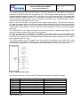
Table 1: HPI signals ........................................................................................................................ 12
Table 2: Valid HPI access combinations ......................................................................................... 13
Table 3: HPI registers...................................................................................................................... 13
Table 4: C6713Compact-2 address map ........................................................................................ 15
Table 5: Default address map of this BSP ...................................................................................... 15
Table 6: Modified address map with CE2 configured for 16 bit....................................................... 16
Table 7: Modified address map with CE2 configured for 8bit.......................................................... 16
Table 8: Modified address map with CE3 configured for 32 bit....................................................... 16
Table 9: Modified address map with CE3 configured for 8 bit......................................................... 17
Table 10: FPGA register locations .................................................................................................. 18
Table 11: FPGA register bit summary in default EMIF configuration .............................................. 18
Table 12: Possible EMIF_CLK settings........................................................................................... 20
Table 13: Timings for the CE2 and CE3 address spaces ............................................................... 21
Table 14: Pinout of micro-line® connectors A through E ................................................................. 22
Table 15: Pinout of micro-line® connector X.................................................................................... 22
Table 16: Recommended operating conditions............................................................................... 27
Table 17: Peripheral interface timings............................................................................................. 28
Table 18: HPI Timings (FPGA part only)......................................................................................... 28
Table 19: HPI register address map................................................................................................ 30
Table 20: HPI register address map using address bit for direction select ..................................... 31
List of Figures
Figure 1: Block diagram of the busmaster BSP ................................................................................ 9
Figure 2: micro-line® peripheral interface ....................................................................................... 10
Figure 3: HPI block diagram............................................................................................................ 11
Figure 4: Available HPI signals ....................................................................................................... 12
Figure 5: IEEE1394 data streaming block diagram......................................................................... 14
Figure 6: Peripheral interface connection example ......................................................................... 29
Figure 7: Host port connections when using a single strobe........................................................... 30
Figure 8: Host port connections when using separate strobe signals ............................................. 30
Figure 9: Host port connections when using address bit for direction selection.............................. 31
Figure 10: Startup message of toggle_led_fpga ............................................................................. 32
Figure 11: Sample asynctst session................................................................................................ 35
Figure 12: Sample isotst session .................................................................................................... 36
Figure 13: Recorded isotst data ...................................................................................................... 37
USER'S GUIDE
MICRO-LINE BUSMASTER BSP
FOR THE C6713COMPACT-2
Date
: 25 June 2012
Doc. no. : C6713Cpt-2_ml_bm_ug
Iss./Rev : 1.0a
Page
:5
1 Preface
1.1
Document Organization
This document is organized as follows:
• Chapter 1 gives some general information such as notational conventions and
documentation overview.
• Chapter 2 introduces the micro-line busmaster® BSP
• Chapter 3 gives an overview of the components that make up the BSP
• Chapter 4 lists the address ranges implemented by the FPGA
• Chapter 5 describes the FPGA registers
• Chapter 6 explains the required EMIF settings
• Chapter 7 gives an overview of the signals available at the micro-line® connector
• Chapter 8 describes each signal in detail
• Chapter 9 lists the electrical characteristics of the available signals
• Chapter 10 lists signal timings
• Chapter 11 gives examples for connecting hardware to the C6713Compact-2
• Chapter 12 describes the application examples available with this BSP
• Chapter 13 lists abbreviations and acronyms used in this document
• Chapter 14 lists further documentation
1.2
Documentation Overview
This chapter lists the documentation from Orsys that is shipped together with software
development kits that contain the micro-line® busmaster BSP. Further documents from other
vendors are listed in chapter and are
referenced throughout the document in square brackets.
C6713Compact-2 Hardware Reference Guide [1] (C6713Cpt-2_hrg.pdf):
Describes the basic hardware (without any FPGA functionality) of the C6713Compact-2.
Flash File System User's Guide [2] (ffs_ug.pdf):
Documents the Flash File System Utilities. Use this document for information on how to store files
in Flash memory.
Board Library User's Guide [3] (boardlib.pdf):
Describes the board library for the C6713Compact-2. Use this document for information on basic
software development.
C6713Compact-2 DM Port Streaming Core User's Guide [4] (C6713Cpt-2_str_core_ug):
Describes the FPGA function block for IEEE1394 software streaming.
IEEE1394 embedded API User's Guide [5] (embedded_API_ug):
Describes the software interface to IEEE1394.
1.3
Notational Conventions
Names of registers, bit fields and single bits are written in capital letters.
Example: LLC_VERSION
Names of signals are also given in capital letters, active low signals are marked with a '/' at the
beginning of the name.
Example: /RESETIN
Date
: 25 June 2012
Doc. no. : C6713Cpt-2_ml_bm_ug
Iss./Rev : 1.0a
Page
:6
USER'S GUIDE
MICRO-LINE BUSMASTER BSP
FOR THE C6713COMPACT-2
Configuration parameters, function names, path names and file names are written in italic typeface.
Example: dev_id
Source code, command line examples and text to be entered are given in a small, fixed-width
typeface.
Example: int a = 10;
Menus and commands from menus and submenus are enclosed in double-quotes. Example:
Create a new project using the "Create Project..." command from the "File" menu.
Keys to type on the keyboard are shown with a surrounding frame, e.g. F10. If a sequence of keys
is to be typed, the keys are separated by commas: F10, ↵. If two keys must be pressed
simultaneously, the key combination is shown with a plus sign: Alt + F.
The members of a bit field or a group of signals are numbered starting at zero, which is the least
significant bit.
Example: CFG[4:0] identifies a group of five signals, where CFG0 is the least significant bit and
CFG4 is the most significant bit.
If necessary, numbers are represented with a suffix that specifies their base.
Example: 12AB16 is a hexadecimal number (base 16 = hexadecimal) and is equal to 477910.
The bit fields of a register are displayed with the most significant bit to the left. Below each bit field
is a description of its read / write accessibility and its default value:
bit number
bit name
15
14
13
12
11
10
6
5
4
3
2
1
0
A
B
C
D
E
F
9
G
8
7
H
I
J
K
L
N
O
r,w,0
r,w,0
r,w,0
r,w,0
r,w,0
r,w,0
r,w,0102
r,0
r,wc,0
w
r,w,0
rc,0
r,w,0
r,w,0
accessibility and default value
legend:
r
bit is readable
rc
this bit is cleared after a read
r,w bit is readable and writeable, reading yields the previously written value unless otherwise
specified.
w
bit is writeable, read value is undefined
wc writing a '1' to this bit clears it
w,0 bit is write-only, reading always yields 0.
0
default value
1.4
Trademarks
TI, Code Composer, DSP/BIOS and TMS320C6000 are registered trademarks of Texas
Instruments.
Microsoft® and Windows® are either registered trademarks or trademarks of Microsoft Corporation
in the United States and/or other countries.
Hyperterminal is a trademark of Hilgraeve Inc.
USER'S GUIDE
MICRO-LINE BUSMASTER BSP
FOR THE C6713COMPACT-2
Date
: 25 June 2012
Doc. no. : C6713Cpt-2_ml_bm_ug
Iss./Rev : 1.0a
Page
:7
All other brand or product names are trademarks or registered trademarks of their respective
companies or organizations.
1.5
Revision History
Revision
v1.0
v1.0a
Changes
First official release
Examples: BIOS configuration documented.
USER'S GUIDE
MICRO-LINE BUSMASTER BSP
FOR THE C6713COMPACT-2
Date
: 25 June 2012
Doc. no. : C6713Cpt-2_ml_bm_ug
Iss./Rev : 1.0a
Page
:8
2 Introduction
This board support package allows to use the C6713Compact-2 as a conventional micro-line® CPU
board. It defines the function of the signals on the micro-line® connector similar to those of other
micro-line® CPU modules, such as the micro-line® C6211CPU board, providing an easy to use
peripheral interface. Further, this BSP provides FIFO-buffered access to the data mover port of the
IEEE1394 chipset for high speed IEEE1394 data streaming.
The functions provided on the micro-line® connectors are:
• micro-line® bus master signals as mentioned in [1] (reset outputs, external flag I/O, RS-232
interface, DSP peripherals). These signals are always present, independent of this BSP.
• micro-line® peripheral interface
• host port interface (HPI)
With the micro-line® peripheral interface, peripherals can be easily connected to the
C6713Compact-2, using no or only minimal glue logic.
The HPI allows other CPUs to access the C6713Compact-2 as a peripheral (e.g. for interprocessor communication).
The software interface is similar to those of the C6x1xCPU and the SC1394a, so software can be
easily ported from the micro-line® C6x1xCPU or the Complete II to the C6713Compact-2.
This BSP should be chosen for
• migration from previous micro-line® CPU modules to the C6713Compact-2
• migration from the micro-line® Complete II to the C6713Compact-2
• accessing micro-line® peripheral modules
• using the micro-line® peripheral interface to connect custom hardware
• software access to IEEE1394 streaming data
• connecting the C6713Compact-2 to a host CPU using the DSP's HPI.
This document describes the features of the BSP solely. The basic features (FPGA independent)
of the C6713Compact-2 are documented in [1].
Please note: To use this BSP, the FPGA must first be loaded with the appropriate code. How to do
this is shown in the application examples, see chapter 12.1.1.
USER'S GUIDE
MICRO-LINE BUSMASTER BSP
FOR THE C6713COMPACT-2
Date
: 25 June 2012
Doc. no. : C6713Cpt-2_ml_bm_ug
Iss./Rev : 1.0a
Page
:9
3 Functional Overview
Figure 1: Block diagram of the busmaster BSP
micro-line® Peripheral Interface
3.1
The micro-line® peripheral interface provides a straightforward connection to up to seven
peripheral boards or custom hardware devices without glue-logic. Its functionality is basically the
same as the direct connection to the TMS320C6713 EMIF in asynchronous operation mode, or to
the parallel bus of many other standard DSPs or micro-controllers. Each bus cycle consists of a
setup, a strobe and a hold phase. Timing of each phase can be programmed to 1 to 15 EMIF
clocks.
On the C6713Compact-2, the micro-line® peripheral interface basically consists of
•
•
•
•
•
32 data bus lines
24 address bus lines (only the lower 16 are actually used)
7 chip select lines
5 interrupt lines
a number of control lines.
Connection examples for the micro-line® peripheral interface can be found in chapter 11.1.
USER'S GUIDE
MICRO-LINE BUSMASTER BSP
FOR THE C6713COMPACT-2
Date
: 25 June 2012
Doc. no. : C6713Cpt-2_ml_bm_ug
Iss./Rev : 1.0a
Page
: 10
Figure 2: micro-line® peripheral interface
Figure 2 gives an overview of the available signals and their direction. For a detailed description of
the individual signals, please refer to chapter 8.1.
Chip select lines /CS1 … /CS3 are mapped into CE space 2 of the TMS320C6713 DSP. This CE
space is configured for 32-bit accesses by default. The remaining chip select lines /CS4 … /CS7
are mapped into CE3, which is configured for 16-bit bus width by default. For further details on
address mapping and bus width configuration, please refer to chapter 4.
Access cycles
The peripheral interface generates a 3-phase bus cycle, independent of the EMIF settings. The list
below shows the steps being performed:
• When the peripheral interface is accessed, the DSPs ready line is deactivated to hold the
current EMIF cycle until the peripheral interface has finished its access.
• At the beginning of the setup phase,
o D[31:0] is driven with the current write data (for write accesses only)
o A[23:16] stay driven low
o A[15:0] are driven with the current address (with in the addressed chip select range)
o The /CS output of the addressed chip select is driven low while the other /CS lines
stay high
o R/W is driven low for write cycles and high for read cycles
• The setup phase has a programmable width of 1 to 7 EMIF clocks, resulting in a setup
period of 10 to 70 ns.
USER'S GUIDE
MICRO-LINE BUSMASTER BSP
FOR THE C6713COMPACT-2
Date
: 25 June 2012
Doc. no. : C6713Cpt-2_ml_bm_ug
Iss./Rev : 1.0a
Page
: 11
•
The setup phase is followed by the strobe phase. At the beginning of the strobe phase,
o /RD is driven low in case of a read cycle
o /WR is driven low in case of a write cycle
o /STRB is driven low
o All other signals remain unchanged
• The strobe phase has a programmable width of 1 to 15 EMIF clocks, resulting in a strobe
period of 10 to 150 ns.
• RDY is sampled 4 EMIF clocks before the end of the strobe phase, see chapter 10.1 for
timing details. RDY allows slow peripherals to extend the strobe phase beyond 15 clocks.
• The strobe phase is followed by the hold phase. At the beginning of the hold phase,
o read data is sampled (in case of a read cycle)
o /RD, /WR and /STRB are driven high
• The hold phase has a programmable width of 1 to 15 EMIF clocks, resulting in a hold
period of 10 to 150 ns.
• At the end of the hold phase,
o D[31:0] are switched to high impedance
o /CS[7:1] are all driven high (switching off the activated chip select line)
o the ARDY line of the DSP is released so that the DSP can finish the current EMIF
access cycle
Timing diagrams can be found in chapter 10.1.
The timing parameters of the peripheral interface can be adjusted by writing to the CSCTL register,
see chapter 5.2.1.
Peripheral devices may extend the strobe phase of a peripheral interface access by hardware
using the RDY input. This allows
•
•
to access very slow peripherals, that require even slower timings than the peripheral
interface supports
to access slow peripherals with the correct timing, while faster peripherals are accessed
with unexpanded bus cycles.
De-asserting the ready (RDY) input line of the micro-line® peripheral interface during an I/O access
will keep the processor in a permanent wait-state as long as the RDY input line will remain inactive.
Only the assertion of the RDY input line will finalize the pending I/O bus cycle and allow the
processor to continue operation. If external hardware controlled I/O access timings are not
required, the RDY input line of the micro-line® peripheral interface should be left unconnected.
How to access peripherals from application software is described in chapter 12.1.2.
3.2
Host Port Interface (HPI)
Figure 3: HPI block diagram
The TMS320C6713 DSP provides a 16 bit wide host port interface (HPI) which can be used by a
host processor to directly access the memory of the DSP. Here, the host device accesses the HPI
USER'S GUIDE
MICRO-LINE BUSMASTER BSP
FOR THE C6713COMPACT-2
Date
: 25 June 2012
Doc. no. : C6713Cpt-2_ml_bm_ug
Iss./Rev : 1.0a
Page
: 12
as a master and the DSP acts as a slave. The host processor and the DSP can exchange
information via DSP-internal and on-board memory. The host also has direct access to memorymapped peripheral registers of the DSP. Connectivity to the DSP memory space is automatically
provided through a DMA mechanism. The host device controls the HPI transfers via dedicated HPI
address and data registers which are not accessible for the DSP. Here, the DMA auxiliary channel
connects the HPI to the DSP memory space.
Both, the host and the DSP can access the HPI control register (HPIC). The host can access the
HPI address register (HPIA), the HPI data register (HPID) and the HPIC by using the external host
port data and control signals. The host can also access the HPI data register in an auto-increment
mode (HPIDA), which allows to read a contiguous block of data without writing to the HPIA register
each time.
The TMS320C6713 can trigger interrupts on the host processor to initiate data transfers. This
avoids unnecessary status polling by the host processor.
The host port data and control signals are available on the micro-line® bus at connector BB. Host
port byte accesses are not supported. Therefore no byte select control signal is provided on the
micro-line® bus. Furthermore no multiplexed data and address busses are supported. The DSP's
control signal /HAS is not used.
The FPGA connects the HPI signals form the micro-line connectors to the DSP's HPI using
combinational logic, adding some delay. The resulting host port timings of the C6713Compact-2
are described in chapter 10.2. Further details about TMS320C6713 HPI can be found in [11].
Figure 4: Available HPI signals
The host port interface on the micro-line® connectors consists of the following signals:
Signal
HD0…HD15
HA0…HA2
/HCS
/HRD
/HWR1
HR/W
HRDY
/HINT
description
host port data bus (input/output)
host port address bus (input)
host port chip select (input)
host port read strobe (input)
host port write strobe (input)
host port read/write select (input)
host port ready (output)
host port interrupt (output)
Table 1: HPI signals
associated with DSP signal
HD[15:0]
HHWIL, HCNTL[1:0]
/HCS
/HDS[2:1] (read access only)
/HDS[2:1] (write access only)
HR/W
HRDY
/HINT
USER'S GUIDE
MICRO-LINE BUSMASTER BSP
FOR THE C6713COMPACT-2
Date
: 25 June 2012
Doc. no. : C6713Cpt-2_ml_bm_ug
Iss./Rev : 1.0a
Page
: 13
There are two different host port hardware operation modes possible. The first one allows to
connect a host with separate strobe signals to the board, using the signals /HCS (chip select),
/HRD (read) and /HWR (write), while HR/W (read/write) must also be connected to /HWR. The
second one allows to connect a host with common strobe to the board, using the signals /HCS
(chip select), HR/W (read/write) and a strobe signal, which must be connected to both, /HRD, while
/HWR must be connected to 1. Chapter 11.2 contains connection examples.
HPI control signal
Access type
/HCS
/HRD
/HWR
/HR/W
0
0
0
0
ignored
0
0
0
1
ignored
0
0
1
0
write access (common strobe configuration)
0
0
1
1
read access (both configurations)
0
1
0
0
write access (separate strobe configuration)
0
1
0
1
ignored
0
1
1
0
ignored
0
1
1
1
ignored
1
x
x
x
ignored
Table 2: Valid HPI access combinations
The functions of the host port addresses are specified in Table 3:
Address
Description
HA2 HA1
HA0
0
0
0
host port interface control register (HPIC), 1st halfword
0
0
1
host port interface control register (HPIC), 2nd halfword
0
1
0
host port interface address register (HPIA), 1st halfword
0
1
1
host port interface address register (HPIA), 2nd halfword
1
0
0
host port interface data register with auto increment (HPIDA), 1st halfword
1
0
1
host port interface data register with auto increment (HPIDA), 2nd halfword
1
1
0
host port interface data register (HPID), 1st halfword
1
1
1
host port interface data register (HPID), 2nd halfword
Table 3: HPI registers
The HPI data are only driven in the respective direction when a valid access is detected. This helps
to avoid bus contention.
3.3
IEEE1394 Data Streaming
The IEEE1394 chipset of the C6713Compact-2 provides a direct access to IEEE1394 data through
the data mover port of the link layer controller (LLC). The data mover port can operate in parallel
with software accesses to the LLC's microcontroller interface. Date transfers are buffered by an
8Kbyte FIFO. The DSP accesses FIFO data through the STR_DATA register; see chapter 5.1 for
details.
USER'S GUIDE
MICRO-LINE BUSMASTER BSP
FOR THE C6713COMPACT-2
Date
: 25 June 2012
Doc. no. : C6713Cpt-2_ml_bm_ug
Iss./Rev : 1.0a
Page
: 14
Figure 5: IEEE1394 data streaming block diagram
The default transfer method for data streaming is isochronous streaming (see [24] for details). The
FPGA can be set up to receive data payload only (from the LLC), so that user data can be
transferred transparently without the need to insert or remove protocol information into or from the
data stream. On the other hand, the FPGA can be configured for complete packet information. This
allows for example, synchronization information to be inserted into the data stream or to
synchronize an incoming image data stream to a frame boundary. The respective data formats are
shown in [4].
For setting up and controlling data streaming, the FPGA provides a set of registers. These are
summarized in chapter 5.1 and described in detail in [4]. Please note that data streaming also
requires set up of the LLC, which is usually done using the IEEE1394 embedded API [5]. How to
set up isochronous streaming is shown in application example isotst. Please refer to chapter 12.1.4
and the example's source code for further information.
USER'S GUIDE
MICRO-LINE BUSMASTER BSP
FOR THE C6713COMPACT-2
Date
: 25 June 2012
Doc. no. : C6713Cpt-2_ml_bm_ug
Iss./Rev : 1.0a
Page
: 15
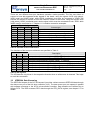
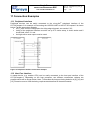
4 Address Map
4.1
C6713Compact-2 Address Map
The table below shows how the 4Gbyte address space of the C6713Compact-2 is used. From this
address space, CE spaces CE2 and CE3 are used by the micro-line® busmaster BSP.
address range (hex)
0000 0000 – 7FFF FFFF
8000 0000 – 8FFF FFFF
9000 0000 – 9FFF FFFF
A000 0000 – AFFF FFFF
B000 0000 – BFFF FFFF
C000 0000 – FFFF FFFF
CE space
none
CE0
CE1
CE2
CE3
reserved
size (bytes)
2G
256M
256M
256M
256M
1G
description
internal memory and on-chip peripherals
external memory (SDRAM)
on-board peripherals
FPGA registers and
micro-line® peripheral interface
reserved
Table 4: C6713Compact-2 address map
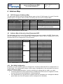
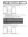
4.2
Address Map of the micro-line® Busmaster BSP
The table below show, how the CE2 and CE3 address spaces are used by this BSP. Please note,
that the addresses refer to the default EMIF configuration, where CE2 is configured for 32 bit
accesses and CE3 is configured for 16-bit accesses.
address range (hex)
A000 0000 – A000 003F
A000 0040 – A003 FFFF
A004 0000 – A007 FFFF
A008 0000 – A00B FFFF
A00C 0000 – A00F FFFF
A010 0000 – A013 FFFF
A014 0000 – AFFF FFFF
B000 0000 – B001 FFFF
B002 0000 – B003 FFFF
B004 0000 – B005 FFFF
B006 0000 – B007 FFFF
B008 0000 – B009 FFFF
B00A 0000 – B00F FFFF
B010 0000 – B010 0007
B010 0008 – BFFF FFFF
CE space
CE2
CE3
size (bytes)
64
256K-64
256K
256K
256K
256K
255M-256K
128K
128K
128K
128K
128K
384K
8
255M-8
description
streaming port registers
reserved
micro-line® CS1 (32 bit)
micro-line® CS2 (32 bit)
micro-line® CS3 (32 bit)
CSCTL register
reserved
reserved
micro-line® CS4 (16 bit)
micro-line® CS5 (16 bit)
micro-line® CS6 (16 bit)
micro-line® CS7 (16 bit)
reserved
FPGA registers
reserved
Table 5: Default address map of this BSP
4.2.1 Bus Width Configuration
By default, the CE2 address space is configured for 32 bit bus width and CE3 is configured for 16
bit bus width. This configuration allows a wide range of peripherals to be connected and can be
used in almost any cases.
However, in some special situations, it may be necessary to change the bus width, e.g. when
• more than three 32-bit chip select lines are needed (then CE3 must be configured to 32 bit,
so that /CS[7:4] are also available for 32 bit peripherals)
• 8 bit peripherals are used and their registers must be accessible as a contiguous address
space (then one of the CE spaces must be configured for 8 bit width)
USER'S GUIDE
MICRO-LINE BUSMASTER BSP
FOR THE C6713COMPACT-2
Date
: 25 June 2012
Doc. no. : C6713Cpt-2_ml_bm_ug
Iss./Rev : 1.0a
Page
: 16
Changing the bus width is done together with setting up EMIF timings, see chapter 6. When the
bus width is changed, the address map (base addresses and size of the address range) also
changes. The resulting addresses are listed in the following tables.
Please note that reconfiguration of the bus width can disable access to IEEE1394 data streaming
or to the FPGA registers as shown in the tables below.
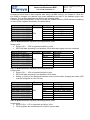
address range (hex)
A000 0000 – A000 001F
A000 0020 – A001 FFFF
A002 0000 – A003 FFFF
A004 0000 – A005 FFFF
A006 0000 – A007 FFFF
A008 0000 – A009 FFFF
A00A 0000 – AFFF FFFF
CE space
CE2
size (bytes)
32
128K-16
128K
128K
128K
128K
256M-640K
description
reserved
reserved
micro-line® CS1 (8 bit)
micro-line® CS2 (8 bit)
micro-line® CS3 (8 bit)
reserved
reserved
Table 6: Modified address map with CE2 configured for 16 bit
Usage notes:
• Each of CS1 … CS3 is organized as 64K by 16 bit
• IEEE1394 data streaming is not possible (32-bit wide data register can't be accessed)
address range (hex)
A000 0000 – A000 000F
A000 0010 – A000 FFFF
A001 0000 – A001 FFFF
A002 0000 – A002 FFFF
A003 0000 – A003 FFFF
A004 0000 – A004 FFFF
A005 0000 – AFFF FFFF
CE space
CE2
size (bytes)
16
64K-16
64K
64K
64K
64K
256M-320K
description
reserved
reserved
micro-line® CS1 (8 bit)
micro-line® CS2 (8 bit)
micro-line® CS3 (8 bit)
reserved
reserved
Table 7: Modified address map with CE2 configured for 8bit
Usage notes:
• Each of CS1 … CS3 is organized as 64K by 8 bit
• IEEE1394 data streaming is not possible in 8-bit mode
• Setting up timing of the peripheral interface must be done before changing bus width (CE2
must be configured for 16 or 32 bits)
address range (hex)
B000 0000 – B003 FFFF
B004 0000 – B007 FFFF
B008 0000 – B00B FFFF
B00C 0000 – B00F FFFF
B010 0000 – B013 FFFF
B014 0000 – B01F FFFF
B020 0000 – B020 000F
B020 0010 – BFFF FFFF
CE space
CE3
size (bytes)
256K
256K
256K
256K
256K
768K
16
254M-16
description
reserved
micro-line® CS4 (16 bit)
micro-line® CS5 (16 bit)
micro-line® CS6 (16 bit)
micro-line® CS7 (16 bit)
reserved
FPGA registers
reserved
Table 8: Modified address map with CE3 configured for 32 bit
Usage notes:
• Each of CS4… CS7 is organized as 64K by 32 bit
• FPGA registers are intersected with 16 bits of unused data
USER'S GUIDE
MICRO-LINE BUSMASTER BSP
FOR THE C6713COMPACT-2
address range (hex)
B000 0000 – B000 FFFF
B001 0000 – B001 FFFF
B002 0000 – B003 FFFF
B003 0000 – B004 FFFF
B004 0000 – B005 FFFF
B005 0000 – B007 FFFF
B008 0000 – B008 0003
B008 0004 – BFFF FFFF
CE space
CE3
size (bytes)
64K
64K
64K
64K
64K
192K
4
255.5M-4
Date
: 25 June 2012
Doc. no. : C6713Cpt-2_ml_bm_ug
Iss./Rev : 1.0a
Page
: 17
description
reserved
micro-line® CS4 (16 bit)
micro-line® CS5 (16 bit)
micro-line® CS6 (16 bit)
micro-line® CS7 (16 bit)
reserved
FPGA registers
reserved
Table 9: Modified address map with CE3 configured for 8 bit
Usage notes:
• Each of CS4… CS7 is organized as 64K by 8 bit
• Access to FPGA registers is limited. The following bit fields are no longer accessible:
o Register VERSION, bit field VERSION
o Register INT_CTL, bit field DM_INT
Date
: 25 June 2012
Doc. no. : C6713Cpt-2_ml_bm_ug
Iss./Rev : 1.0a
Page
: 18
USER'S GUIDE
MICRO-LINE BUSMASTER BSP
FOR THE C6713COMPACT-2
5 Register Description
5.1
IEEE1394 Streaming Registers
The registers used for IEEE1394 streaming are documented in [3]. One additional register provides
access to streaming data. This register must always be accessed as 32 bits. The table below
shows the register locations.
Register
Address (hex)
width
STR_CTL
A000 0000
16 bit
reserved
A000 0004
n/a
STR_HDR_L
A000 0008
16 bit
STR_HDR_H
A000 000C
16 bit
reserved
A000 0010
n/a
reserved
A000 0014
n/a
STR_AFL
A000 0018
16 bit
STR_AEL
A000 001C
16 bit
STR_IE
A000 0020
16 bit
STR_IF
A000 0024
16 bit
reserved
A000 0028
n/a
reserved
A000 002C
n/a
reserved
A000 0030
n/a
STR_LEVEL
A000 0034
16 bit
STR_DATA
A000 0038
32 bit
reserved
A000 003C
n/a
5.2
FPGA Registers
Table 10 lists the register addresses. Default configuration is listed in bold.
register
description
address
8 bit bus width
16 bit bus width
CSCTL
controls chip select timing
A004 0000h
A008 0000h
VERSION FPGA version
B008 0000h
B010 0000h
LED_CTL LED control
B008 0001h
B010 0002h
CLK_CTL controls clock output
B008 0002h
B010 0004h
INT_CTL interrupt polarity & selection
B008 0003h
B010 0006h
32 bit bus width
A010 0000h
B020 0000h
B020 0004h
B020 0008h
B020 000Ch
Table 10: FPGA register locations
Name
Addr.
CSCTL
VERSION
LED
EMIF_CLK
INT_CTL
A0100000
B0100000
B0100002
B0100004
B0100006
15-10
9
8
RESERVED
VERSION
RESERVED
RESERVED
RESERVED
STR_INTSEL
7
6
5
SETUP
LED_GREEN
EINT7_POL
LED_RED
CLK_EN
EINT6_POL
4
3
2-0
STRB
HLD
REVISION
RESERVED
DIV
RESERVED
EINT5_POL
ENT4_POL
NMI_POL
RESERVED
Table 11: FPGA register bit summary in default EMIF configuration
5.2.1 Chip Select Control Register
This register controls timing of the peripheral interface.
15
14
13
12
11
10
9
8
7
6
5
4
3
2
1
RESERVED
SETUP
STROBE
HOLD
r,0000000
r,w,001
r,w,001
r,w,001
0
Date
: 25 June 2012
Doc. no. : C6713Cpt-2_ml_bm_ug
Iss./Rev : 1.0a
Page
: 19
USER'S GUIDE
MICRO-LINE BUSMASTER BSP
FOR THE C6713COMPACT-2
SETUP controls the number of EMIF clocks for the setup phase. Default value is 1 clock, a value of
0 is treated as a value of 1. Allowable range is 1 to 7.
STROBE controls the number of EMIF clocks for the strobe phase. Default value is 1 clock, a value
of 0 is treated as a value of 1. Allowable range is 1 to 7.
HOLD controls the number of EMIF clocks for the hold phase. Default value is 1 clock, a value of 0
is treated as a value of 1. Allowable range is 1 to 7.
5.2.2 FPGA Version Register
This register describes the FPGA version and revision. Application software can use this register to
check, if the correct FPGA code is loaded. This register is read-only.
15
14
13
12
11
10
9
8
7
6
5
4
3
2
VERSION
REVISION
r,00000011
r
1
0
VERSION
This bit field describes the FPGA version. Each BSP has a unique version. This BSP uses version
number 3. The version field can be used by application software to verify that the correct BSP is
loaded.
REVISION
This bit field describes BSP revision. The revision can change due to product improvement.
5.2.3 LED Control Register
This register controls the two LEDs that are connected to the FPGA. The LEDs can be used as
status indicators by application software, e.g.
•
the green LED is switched on during signal processing to show activity
•
the red LED can be switched on when errors are detected
15
14
13
7
6
RESERVED
12
11
10
9
8
LED_GREEN
LED_RED
5
RESERVED
4
3
2
1
0
r,00000000
r,w,0
r,w,0
r,000000
LED_GREEN
This bit controls the green LED. Setting this bit to 1 will cause the green LED to light. By default,
the green LED is off.
LED_RED
This bit controls the red LED. Setting this bit to 1 will cause the red LED to light. By default, the red
LED is off.
5.2.4 Clock Control Register
This register controls the EMIF_CLK output on the micro-line® connector. This signal is generated
from the DSP's EMIF clock. Please note that changing the EMIF_CLK on the micro-line®
connector does not change the EMIF clock of the DSP. All timings based on the EMIF clock (such
as SDRAM timings or the asynchronous timings of the seven micro-line® chip select lines) remain
unchanged.
15
14
13
12
11
10
9
8
7
6
RESERVED
CLK_EN
r,000000000
r
5
4
DIV
3
2
1
0
RESERVED
CLK_EN
If this bit is set, the EMIF_CLK output is driven. If this bit is set to 0, the EMIF_CLK line is in high
impedance state. This bit can be used to reduce EMI when EMIF_CLK if it is not used. Changing
CLK_EN is synchronized to the clock output to allow glitch-free switching.
DIV
USER'S GUIDE
MICRO-LINE BUSMASTER BSP
FOR THE C6713COMPACT-2
Date
: 25 June 2012
Doc. no. : C6713Cpt-2_ml_bm_ug
Iss./Rev : 1.0a
Page
: 20
This bit field controls the frequency of the EMIF_CLK output. By default, DIV is set to 3, which
selects a frequency of a quarter of the EMIF clock (25 MHz at a default EMIF clock of 100 MHz).
Changing DIV is synchronized to the clock output to allow glitch-free switching. Together with
CLK_EN, the following selections are possible:
CLK_EN
0
1
DIV
(don't care)
0
1
2
3
EMIF clock output
Z
0
undivided EMIF clock
EMIF clock
2
EMIF clock
4
Table 12: Possible EMIF_CLK settings
5.2.5 Interrupt Control Register
This register has two purposes:
• it controls the polarity for the interrupt sources on the micro-line® bus
• it selects the interrupt line that is used for IEEE1394 data streaming.
15-10
RSV
r,000000
9
8
7
STR_INTSEL EINT7_POL
6
5
4
3
2-0
EINT6_POL EINT5_POL EINT4_POL NMIPOL RSV
r,w,00
r,w,00000
r,000
STR_INTSEL
This bit field selects the interrupt line for streaming. Default value is 0, so DSP external interrupt 4
is used.
STR_INTSEL
0
1
2
3
interrupt line
EXT_INT4
EXT_INT5
EXT_INT6
EXT_INT7
EINT4_POL ... EINT7_POL,
NMI_POL
These bits control the polarity of the interrupt inputs at the micro-line® connector. This gives the
user more flexibility in connecting peripherals to the C6713Compact-2. By default, all bits are 0,
which selects falling edge triggered interrupts (in contrast to the DSP interrupts, which are rising
edge triggered by default). If an interrupt source with rising edge triggered interrupts is connected
to the micro-line® bus, the corresponding polarity bit needs to be set. Please do not change the
interrupt polarity in the DSP's registers. The micro-line® interrupts trigger the corresponding
interrupts on the DSP. However, some more interrupt sources exist on the C6713Compact-2.
Therefore, application software must check all possible interrupt sources. The other interrupt
sources are described in [1].
EINTx_POL, NMI_POL
0
1
micro-line® interrupts
falling edge triggered
rising edge triggered
USER'S GUIDE
MICRO-LINE BUSMASTER BSP
FOR THE C6713COMPACT-2
Date
: 25 June 2012
Doc. no. : C6713Cpt-2_ml_bm_ug
Iss./Rev : 1.0a
Page
: 21
6 Setting up EMIF Timings
This chapter shows how the EMIF must be set up for using the micro-line® busmaster BSP.
By default, the Flash File System sets up the EMIF timings for the CE2 and CE3 address space to
a slow and safe default. This default works with the micro-line® busmaster BSP, however, using
the default setting does not give optimum performance, so the user may want to modify EMIF
settings. How to program this is shown in the examples on the distribution media and in the board
library documentation. The actual timings depend on which parts of the BSP are being used.
There is an absolute minimum, which can be used for register accesses only, excluding the
peripheral interface and streaming data. When using this setup, accesses to the FPGA may
include a one-clock wait cycle which slows down operation.
There is also a recommended minimum, which allows register accesses without wait states and
also allows accessing the peripheral interface (which always inserts waitstates).
For reading streaming data from the FIFO, the entire cycle time must be increased by 1 clock to
allow FIFO data to update in time when doing back-to-back read cycles.
Table 13 lists the default timings set up by the Flash File System and the timings required for
operation of the micro-line® busmaster BSP.
parameter
read setup
read strobe
read hold
turnaround
write setup
write strobe
write hold
Required setting in EMIF clocks
FFS default Absolute
Recommended minimum /
minimum
peripheral interface
5
1
2
25
2
2
3
1
1
1
1
1
5
1
2
25
2
2
3
1
1
Streaming
3
2
1
1
2
2
1
Table 13: Timings for the CE2 and CE3 address spaces
Note: Setting up EMIF timings is done together with setting up the memory type, which in turn
defines the actual bus width.
USER'S GUIDE
MICRO-LINE BUSMASTER BSP
FOR THE C6713COMPACT-2
Date
: 25 June 2012
Doc. no. : C6713Cpt-2_ml_bm_ug
Iss./Rev : 1.0a
Page
: 22
7 Signals on the micro-line Connector
This chapter lists the signals on the micro-line® connectors that are defined by this BSP. For a
description of the remaining signals and connector locations, please refer to [1]. Entries labeled
"RSV" are connected to the FPGA but are not used. They have pull-up termination in the FPGA.
Shaded entries are provided by basic board hardware, independent of the micro-line® busmaster
BSP.
Connector
Pin
1
2
3
4
5
6
7
8
9
10
11
12
13
14
15
16
17
18
19
20
21
22
23
24
25
26
27
28
29
30
31
32
A
D0 (I/O/Z)
D1 (I/O/Z)
D2 (I/O/Z)
D3 (I/O/Z)
D4 (I/O/Z)
D5 (I/O/Z)
D6 (I/O/Z)
D7 (I/O/Z)
D8 (I/O/Z)
D9 (I/O/Z)
D10 (I/O/Z)
D11 (I/O/Z)
D12 (I/O/Z)
D13 (I/O/Z)
D14 (I/O/Z)
D15 (I/O/Z)
D16 (I/O/Z)
D17 (I/O/Z)
D18 (I/O/Z)
D19 (I/O/Z)
D20 (I/O/Z)
D21 (I/O/Z)
D22 (I/O/Z)
D23 (I/O/Z)
D24 (I/O/Z)
D25 (I/O/Z)
D26 (I/O/Z)
D27 (I/O/Z)
D28 (I/O/Z)
D29 (I/O/Z)
D30 (I/O/Z)
D31 (I/O/Z)
B
A0 (O)
A1 (O)
A2 (O)
A3 (O)
A4 (O)
A5 (O)
A6 (O)
A7 (O)
A8 (O)
A9 (O)
A10 (O)
A11 (O)
A12 (O)
A13 (O)
A14 (O)
A15 (O)
A16 (O)
A17 (O)
A18 (O)
A19 (O)
A20 (O)
A21 (O)
A22 (O)
A23 (O)
Signal GND
Signal GND
Signal GND
Signal GND
Signal GND
Signal GND
Signal GND
Signal GND
BB
HD0 (I/O/Z)
HD1 (I/O/Z)
HD2 (I/O/Z)
HD3 (I/O/Z)
HD4 (I/O/Z)
HD5 (I/O/Z)
HD6 (I/O/Z)
HD7 (I/O/Z)
HD8 (I/O/Z)
HD9 (I/O/Z)
HD10 (I/O/Z)
HD11 (I/O/Z)
HD12 (I/O/Z)
HD13 (I/O/Z)
HD14 (I/O/Z)
HD15 (I/O/Z)
HA0 (I)
HA1 (I)
HA2 (I)
RSVD
HR/W (I)
/HCS (I)
/HRD (I)
/HWR (I)
HRDY (O/Z)
/HINT (O/Z)
RSV
RSV
RSV
RSV
RSV
RSV
C
RSV
RSV
RSV
RSV
RSV
RSV
RSV
RSV
RSV
RSV
RSV
RSV
RSV
RSV
RSV
RSV
RSV
RSV
RSV
RSV
RSV
RSV
RSV
RSV
RSV
RSV
RSV
RSV
RSV
RSV
RSV
RSV
D
Power GND (I)
Power GND (I)
Power GND (I)
Power GND (I)
+3.3 to +5V (I)
+3.3 to +5V (I)
/RESETIN (I)
/RESETOUT (O)
RESETOUT (O)
/CS1 (O)
/CS2 (O)
/CS3 (O)
/CS4 (O)
/CS5 (O)
/CS6 (O)
/CS7 (O)
/EXT_INT4 (I)
/EXT_INT5 (I)
/EXT_INT6 (I)
/EXT_INT7 (I)
/NMI (I)
/RD (O)
/WR (O)
R/W (O)
/STRB (O)
TXD (O)
RTS (O)
RXD (I)
CTS (I)
RDY (I)
/HOLD (I)
/HOLDA (O/Z)
Table 14: Pinout of micro-line® connectors A through E
Connector
Pin
1
2
3
4
5
6
7
8
9
10
X
RSV
RSV
RSV
RSV
RSV
RSV
RSV
RSV
RSV
RSV
Table 15: Pinout of micro-line® connector X
E
RSV
RSV
RSV
RSV
RSV
RSV
RSV
RSV
RSV
DR1 (I)
SDA1 (I/O/Z)
DX1 (O/Z)
AXR0[5] (I/O/Z)
CLKR1 (I/O/Z)
AXR0[6] (I/O/Z)
CLKX1 (I/O/Z)
AMUTE0 (O/Z)
FSR1 (I/O/Z)
AXR0[7] (I/O/Z)
FSX1 (I/O/Z)
RSV
CLKS1 (I)
SCL1 (I/O/Z)
TINP1 (I)
AHCLKX0 (I/O/Z)
TINP0 (I)
AXR0[3] (I/O/Z)
CLKS0 (I)
AHCLKR0 (I/O/Z)
DR0 (I)
AXR0[0] (I/O/Z)
DX0 (O/Z)
AXR0[1] (I/O/Z)
CLKR0 (I/O/Z)
ACLKR0 (I/O/Z)
CLKX0 (I/O/Z)
ACLKX0 (I/O/Z)
FSR0 (I/O/Z)
AFSR0 (I/O/Z)
FSX0 (I/O/Z)
AFSX0 (I/O/Z)
XF0 (I/O/Z)
XF1 (I/O/Z)
TOUT0 (O)
AXR0[2] (I/O/Z)
TOUT1 (O)
AXR0[4] (I/O/Z)
UART_CLK (O/Z)
EMIF_CLK (O/Z)
/SHZ (I)
USER'S GUIDE
MICRO-LINE BUSMASTER BSP
FOR THE C6713COMPACT-2
Date
: 25 June 2012
Doc. no. : C6713Cpt-2_ml_bm_ug
Iss./Rev : 1.0a
Page
: 23
8 Individual Signal Description
This chapter describes each signal that is defined by the micro-line® busmaster BSP. The
remaining signals (shaded entries in Table 14) are described in the C6713Compact-2 hardware
reference guide [1].
8.1
micro-line Peripheral Interface
8.1.1 Connector A
D[31:0]:
These are the bi-directional data bus lines of the micro-line® peripheral interface. They are
activated during the strobe phase of an access to the micro-line® peripheral interface. When
inactive, the data bus is in high impedance state.
8.1.2 Connector B
A[15:0]:
These are the address bus output lines of the micro-line® peripheral interface. They are always
active and carry a valid address during the entire access cycle, from start of setup phase until end
of hold phase.
A[23:16]:
These address lines are not used in this BSP. They are always driven low by the FPGA.
8.1.3 Connector D
/CS[7:1]:
These are the seven active low chip select output lines of the micro-line® peripheral interface. They
pre-select, which external peripheral component is accessed and are valid during all three phases
of the access, from start of setup phase until end of hold phase. The seven peripheral address
spaces are located in the processor's CE2 and CE3 address spaces. The chip select lines
/CS1…/CS3 refer to the EMIF CE2 area of the processor and /CS4…/CS7 refer to the EMIF CE3
area of the processor. This allows to connect two different I/O areas with different bus width. The
locations of the seven peripheral address spaces are shown in chapter 4.2.
/RD, /WR:
These are the active low read strobe (/RD) and write strobe (/WR) output lines of the micro-line®
peripheral interface. They indicate a read cycle (/RD) or a write cycle (/WR). The strobe signals are
active during the strobe phase of an access. In case of a read cycle, data is sampled at the rising
edge of /RD. Write data is valid throughout the entire access cycle, from start of setup phase until
end of hold phase. These signals should be used, when separate read and write strobes are
required. Peripherals with a common strobe and a direction select signal should be used with R/W
and /STRB instead.
R/W, /STRB:
These are the read/write (R/W) and the active low strobe (/STRB) output lines of the micro-line®
peripheral interface. They indicate a read cycle (R/W = high and /STRB = low) or a write cycle
(R/W = low and /STRB = low). R/W is valid throughout the entire access cycle, from start of setup
phase until end of hold phase. /STRB is valid during the strobe phase of an access. These signals
should be used to connect peripherals that require a common strobe signal and a direction select
signal. Peripherals with separate read and write strobes should be used with /RD and /WR instead.
RDY:
USER'S GUIDE
MICRO-LINE BUSMASTER BSP
FOR THE C6713COMPACT-2
Date
: 25 June 2012
Doc. no. : C6713Cpt-2_ml_bm_ug
Iss./Rev : 1.0a
Page
: 24
This pin is the active high ready input of the micro-line® peripheral interface. RDY is sampled 4
clocks before the end of the strobe phase. If RDY is sampled low, the strobe period is extended by
one EMIF clock and RDY is sampled again. If RDY is sampled high, the strobe period ends. If no
bus cycle extension is required, RDY should be left unconnected. The necessary pull up resistor is
provided on the C6713Compact-2. This input can be used by
• very slow hardware, whose timing exceeds the maximum timing adjustable in the CSCTL
register
• a mixture of fast and slow peripherals, where the access timing is configured (in CSCTL) for
the fast peripherals, but the slow peripherals can extend the access for their timing
requirements. This way, the slow peripherals don't slow down accesses to the fast ones.
/HOLD, /HOLDA
These signals can be used by an external busmaster, to access on-board peripherals. The
busmaster function is not supported by this BSP. Therefore, these signals should be left
unconnected.
/EXT_INT[7:4]:
These are the four maskable interrupt input lines of the micro-line® peripheral interface. They can
be used as interrupts or for DMA synchronization. In default configuration, all interrupts are
triggered on the falling edge of the interrupt signal (in contrast to the default polarity of the DSP
interrupt lines). They can be individually configured to be either falling edge triggered or rising edge
triggered. This is described in chapter 5.2.5. Level triggering is not possible at the TMS320C6713
DSP. To enable interrupts from the micro-line® peripheral interface, the interrupts must be enabled
by the DSP. Further, /EXT_INT6 and /EXT_INT7 are routed over the PLD of the C6713Compact-2
and must also be enabled there. This is described in [1]. The line status of /EXT_INT7 and
/EXT_INT6 can be polled by PLD status bits, see also [1] for a description.
Please note, that other interrupt sources exist on the C6713Compact-2 for /EXT_INT6 and
/EXT_INT7. Before designing peripheral hardware to use a specific micro-line® interrupt, please
check which on-board interrupt sources of the C6713Compact-2 are used. Shared interrupts can
be used, but avoiding them makes the system easier and faster.
/NMI:
This is the non-maskable interrupt input line of the micro-line® peripheral interface. Activation of
/NMI causes an interrupt at a high priority level which can not be masked by software. In default
configuration, /NMI is triggered on the falling edge of the interrupt signal (in contrast to the DSP's
NMI signals, which is rising edge triggered). It can be configured to be either falling edge triggered
or rising edge triggered. This is described in chapter 5.2.5. Level triggering is not possible.
RESETOUT and /RESETOUT:
These signals are always provided by the C6713Compact-2, independent of this BSP. Please refer
to [1] for a description.
/HOLD, /HOLDA
8.1.4 Connector E
UART_CLK:
This signal is always provided by the C6713Compact-2, independent of this BSP. Please refer to
[1] for a description.
EMIF_CLK:
This pin is the clock output for the micro-line® peripheral interface. This clock is generated from the
DSP's external memory interface clock. The clock output on this pin is software programmable. By
default, the DSP EMIF clock divided by 4 is available on this signal. See chapter 5.2.4 for details.
In order to reduce EMI it is recommended to switch off this signal if it is not used. The clock output
USER'S GUIDE
MICRO-LINE BUSMASTER BSP
FOR THE C6713COMPACT-2
Date
: 25 June 2012
Doc. no. : C6713Cpt-2_ml_bm_ug
Iss./Rev : 1.0a
Page
: 25
has small delay to the DSP's EMIF clock and switches at the same time as all other outputs of the
peripheral interface, see section 10.1 for timing specifications. Please note, that the frequency of
this signal does not affect any timing of the TMS320C6713 EMIF.
8.2
Host Port Interface
8.2.1 Connector BB
HD[15:0]:
These pins are the bi-directional data bus of the host port interface. Data can be directly written to
or read from the whole address space of the TMS320C6713 DSP. The data lines are only
activated when a valid host port access is detected see Table 2. Otherwise, HD[15:0] are in high
impedance state.
HA[2:0]:
These pins are the host port address inputs. They select which 16 bit halfword and which HPI
register is currently accessed by the host. The register map of the host port is given in Table 3.
Connection examples for the host port can be found in chapter 11.2.
/HCS:
This pin is the chip select input of the host port. The host must set /HCS low in order to enable host
port accesses. /HCS must be low during the whole access.
/HRD:
This pin is the read strobe input of the host port. It should be connected either to the host's read
strobe, or to the host's common strobe. Please refer to HPI access decoding in Table 2 and the
connection examples in chapter 11.2 for details.
/HWR:
This pin is the write strobe input of the host port. It should be connected either to the host's write
strobe, or to a permanent high level when using a common strobe. Please refer to HPI access
decoding in Table 2 and the connection examples in chapter 11.2 for details.
HR/W:
This pin is the host read/write select input. The host must set HR/W high in order to read and low in
order to write on the HPI. A host without a read/write select output can connect HR/W to /HWR or
use an address line for this function. Please refer to HPI access decoding in Table 2 and the
connection examples in chapter 11.2 for details.
HRDY:
This pin is the ready output of the host port. When active (high), HRDY indicates that the HPI is
ready for a transfer to be performed. When inactive (low), HRDY indicates that the HPI is busy
completing a read access, a previous HPI data register read pre-fetch or a write access. HRDY is
always high when /HCS is high. Please note that HRDY is inverted with respect to the DSP's lowactive ready output.
/HINT:
This pin is the interrupt output of the host port interface. This interrupt is controlled by the HINT bit
in the HPI control register. It is cleared (set to high level) when the processor is reset. The
TMS320C6713 DSP can trigger an interrupt to the host by setting the HINT bit in the HPIC register.
An interrupt is pending, when /HINT is low. The host can clear the interrupt after processing by
writing a 1 to the HINT bit.
USER'S GUIDE
MICRO-LINE BUSMASTER BSP
FOR THE C6713COMPACT-2
8.3
Date
: 25 June 2012
Doc. no. : C6713Cpt-2_ml_bm_ug
Iss./Rev : 1.0a
Page
: 26
Other Signals
/SHZ
Test pin for factory tests. When /SHZ is activated (driven low), below listed micro-line® pins are
switched to high impedance state:
D[31:0], A[23:0], /CS[7:1], /RD, /WR, R/W, /STRB, EMIF_CLK, HRDY, /HINT, /HOLDA.
The /SHZ input is not designed for use during normal operation and should be left unconnected. A
pull up resistor is implemented by the FPGA.
RSV
Signals listed as 'RSV' in Table 14 and Table 15 are FPGA I/O pins not used by this BSP. The
FPGA pulls these pins high (regardless whether the FPGA is configured or not). Customers should
leave these pins unconnected.
USER'S GUIDE
MICRO-LINE BUSMASTER BSP
FOR THE C6713COMPACT-2
Date
: 25 June 2012
Doc. no. : C6713Cpt-2_ml_bm_ug
Iss./Rev : 1.0a
Page
: 27
9 Signal Levels
All signals described in this document use LVTTL signal levels. The recommended operating
conditions are listed below:
parameter
value
min
max
logic low input voltage
-0.5 V
0.8 V
logic high input voltage
2.0 V
3.6 V
logic low output voltage 1
0.4 V
logic high output voltage
2.4 V
Table 16: Recommended operating conditions
1
at 8mA load (12mA for EMIF_CLK)
Date
: 25 June 2012
Doc. no. : C6713Cpt-2_ml_bm_ug
Iss./Rev : 1.0a
Page
: 28
USER'S GUIDE
MICRO-LINE BUSMASTER BSP
FOR THE C6713COMPACT-2
10 Signal Timings
All timing specifications in this chapter apply to FPGA version 3.0. The timings are based on the
FPGA design and also include some margin for PCB trace delay.
10.1 micro-line Peripheral Interface
All inputs and outputs of the micro-line peripheral interface are synchronized to the EMIF clock.
This gives a well-defined timing with minimum skew.
Parameter
EMIF_CLK valid after rising edge of DSP's ECLKOUT
all other outputs valid after rising edge of DSP's ECLKOUT
read data setup relative to rising edge of /STRB, /RD, /WR
read data hold relative to rising edge of /STRB, /RD, /WR
RDY setup relative to rising edge of /STRB, /RD, /WR
RDY hold relative to rising edge of /STRB, /RD, /WR
delay from /EXT_INT[7:4], /NMI to DSP interrupts
delay between DSP and /HOLD, /HOLDA
Total EMIF cycle time for 1-1-1 (setup-strobe-hold) access
Total EMIF cycle time for 7-7-7 access, immediate ready
Total EMIF cycle time for 7-7-7 access, 1 clock not-ready
min
2 ns
2 ns
8.1 ns
-2 ns
48 ns
-42 ns
max
5 ns
6 ns
23 ns
23 ns
120 ns
300 ns
310 ns
Table 17: Peripheral interface timings
10.2 Host Port Interface
The host port interface is handled by pure combinational logic. Therefore the timings of the DSP's
HPI must be considered in conjunction with the timings specified below.
Parameter
Delay HPI strobe signals from connector to DSP
Skew between strobe signals
Delay HPI select signals from connector to DSP
Skew between select signals
HPI data tristate delay from connector to DSP
HPI data delay from connector to DSP
Skew between HPI data (connector to DSP)
HPI data tri-state delay from connector to connector
HPI data delay from DSP to connector
Skew between HPI data (DSP to connector)
Delay HRDY from DSP to connector
Delay /HINT from DSP to connector
Table 18: HPI Timings (FPGA part only)
min
7.4 ns
7.5 ns
8 ns
6.3 ns
5.5 ns
6.3 ns
8 ns
9.2 ns
max
15 ns
3.5 ns
14.6 ns
3.0 ns
17 ns
13 ns
2.5 ns
16 ns
13 ns
2.5 ns
13 ns
14.5 ns
USER'S GUIDE
MICRO-LINE BUSMASTER BSP
FOR THE C6713COMPACT-2
Date
: 25 June 2012
Doc. no. : C6713Cpt-2_ml_bm_ug
Iss./Rev : 1.0a
Page
: 29
11 Connection Examples
11.1 Peripheral Interface
Peripheral devices can be easily connected to the micro-line® peripheral interface of the
C6713Compact-2. An example of connecting the 16C550 UART to the C6713Compact-2 is shown
below. For this connection example,
• /EXT_INT4 must be configured to be rising-edge triggered, see section 5.2.5,
• timing of the peripheral interface must be set up to 2 clocks setup, 4 clocks strobe and 2
clocks hold, see 5.2.1 and
• the high-active reset output must be used.
Figure 6: Peripheral interface connection example
11.2 Host Port Interface
A master device (e.g. another CPU) can be easily connected to the host port interface of the
C6713Compact-2. Depending on the host processor, two different connections variants are
possible which will be shown below. Note: TI describes the host port timing behavior in [8], [10] and
[15]. Please be sure to fulfill the timing requirements described in these documents.
USER'S GUIDE
MICRO-LINE BUSMASTER BSP
FOR THE C6713COMPACT-2
Date
: 25 June 2012
Doc. no. : C6713Cpt-2_ml_bm_ug
Iss./Rev : 1.0a
Page
: 30
11.2.1 Host Port Connection with Common Strobe and Direction Select
An example for connecting a CPU with common strobe signal to the C6713Compact-2 is shown
below.
Figure 7: Host port connections when using a single strobe
The following steps have to be performed:
• All signals must be connected directly to the respective signal of the C6713Compact-2
except /STRB which must be connected to /HRD.
• /HWR must be pulled high.
• HRDY might need to be inverted, depending on the host CPU type.
• Address offset between HPI registers depends on the host CPU type.
The host CPU uses the following address map:
Address
Register
Base + 00
host port interface control (HPIC), 1st halfword
Base + 01
host port interface control (HPIC), 2nd halfword
Base + 02
host port interface address (HPIA), 1st halfword
Base + 03
host port interface address (HPIA), 2nd halfword
Base + 04
host port interface data with auto increment (HPIDA), 1st halfword
Base + 05
host port interface data with auto increment (HPIDA), 2nd halfword
Base + 06
host port interface data (HPID), 1st halfword
Base + 07
host port interface data (HPID), 2nd halfword
Table 19: HPI register address map
11.2.2 Host Port Connections with Separate Strobe Signals
An example for connecting a CPU with separate strobe signals to the C6713Compact-2 is shown
below.
Figure 8: Host port connections when using separate strobe signals
USER'S GUIDE
MICRO-LINE BUSMASTER BSP
FOR THE C6713COMPACT-2
Date
: 25 June 2012
Doc. no. : C6713Cpt-2_ml_bm_ug
Iss./Rev : 1.0a
Page
: 31
The following steps have to be performed:
• All signals must be connected directly to the respective signal of the C6713Compact-2.
• HR/W must also be connected to the hosts /WR output.
• HRDY might need to be inverted, depending on the host CPU type.
• Address offset between HPI registers depends on the host CPU type.
• Register address map is the same as shown in Table 19
11.2.3 Host Port Connections with Separate Strobe Signals Alternative Method
If timing issues prohibit the use of the host's /WR signal, HR/W can also be connected to the host's
/OE output (if present) or to an additional address bit. table below shows the resulting register
address map when using the host's A3 line for direction selection.
CAUTION:
When connecting an address bit to HR/W, invalid accesses can cause bus contention on
HD[15:0]! Please make sure that the register address corresponds with the access
direction!
Figure 9: Host port connections when using address bit for direction selection
Address
Base + 00
Base + 01
Base + 02
Base + 03
Base + 04
Base + 05
Base + 06
Base + 07
Base + 08
Base + 09
Base + 10
Base + 11
Base + 12
Base + 13
Base + 14
Base + 15
Direction
write only
read only
Register
host port interface control (HPIC), 1st halfword
host port interface control (HPIC), 2nd halfword
host port interface address (HPIA), 1st halfword
host port interface address (HPIA), 2nd halfword
host port interface data with auto increment (HPIDA), 1st halfword
host port interface data with auto increment (HPIDA), 2nd halfword
host port interface data (HPID), 1st halfword
host port interface data (HPID), 2nd halfword
Table 20: HPI register address map using address bit for direction select
USER'S GUIDE
MICRO-LINE BUSMASTER BSP
FOR THE C6713COMPACT-2
Date
: 25 June 2012
Doc. no. : C6713Cpt-2_ml_bm_ug
Iss./Rev : 1.0a
Page
: 32
12 Application Examples
The following application examples are provided with the micro-line® busmaster BSP:
toggle_led
Basic example which is also the default application in FFS; placed in the BSP
for historical reasons only.
toggle_led_fpga Toggles all four user controllable LEDs (2x PLD and 2x FPGA) and shows how
to configure (load) the FPGA
asynctst
Shows how to implement IEEE1394 asynchronous transactions
isotst
Shows how to implement IEEE1394 isochronous streaming
12.1 Default FFS Application (toggle_led)
This application example is not really specific to the micro-line® busmaster BSP. It was put into the
BSP distribution for historical reasons. toggle_led is the default application that is stored in the FFS
during production. It simply enables CTS resets (for connecting with the FFS utilities) and toggles
the red LED.
12.1.1 Loading and Accessing the FPGA (toggle_led_fpga)
The distribution media contains an application example called toggle_led_fpga. This example
shows
• How to load the FPGA from within application software using the board library
• How to access the FPGA registers (using the LED control register).
Please note: The FPGA can also be loaded through the Flash File System, see [2] for details.
To start this example you have to
• Connect the RS-232 interface of the C6713compact-2 to your development PC.
• Load the toggle_led_fpga example to the C6713Compact-2 using the fload6x utility. How to
do this is described in the "Getting started" section of the respective development kit user's
guide and also in [2]
• power-off the C6713Compact-2
• Start a terminal program, such as Hyperterminal
• power-on the C6713Compact-2
• Now you see the startup message of toggle_led_fpga in the terminal window and the LEDs
of the C6713Compact-2 start to toggle.
C6713Compact-2 application example toggle_led_FPGA Feb 12 2012 15:55:58
FPGA loaded
Figure 10: Startup message of toggle_led_fpga
This example contains two modules: toggle_led_fpga.c which contains example code itself and the
FPGA code for the micro-line® busmaster BSP which is contained in ml_bm_fpga_lx<DEV>.c,
where <DEV> is for the respective FPGA type, e.g. 75 for an LX75.
The project that builds the example has different configurations, one for each supported FPGA
type. The generated code is therefore specific to a certain FPGA type.
12.1.2 Micro-line® Peripheral Interface
There is no specific application example for accessing peripherals, because it would require some
peripheral connected to the C6713Compact-2. However, accessing peripherals is straightforward
and is described below:
The base addresses of each chip select are defined in C-headers that are delivered together with
the C6713Compact-2. To access a peripheral device consider the following example:
USER'S GUIDE
MICRO-LINE BUSMASTER BSP
FOR THE C6713COMPACT-2
Date
: 25 June 2012
Doc. no. : C6713Cpt-2_ml_bm_ug
Iss./Rev : 1.0a
Page
: 33
• A peripheral device is connected to /CS1.
• Two locations are decoded by using the micro-line® address bus:
A0 = 0: control and status register, 8 bit wide, D0 indicates data is available
A0 = 1: data register, 16 bit wide
/CS1 is located within the CE2 address space, which is by default configured for 32 bit wide
memory. Therefore, each address within /CS1 contains 32 bits and the (DSP) address offset
between subsequent locations is 4 bytes. The code example below shows how to define access
macros to the peripheral and how to access the peripheral.
#include "C6713Cpt-2_ml_bm.h" /* micro-line busmaster BSP definitions */
#define MY_CSR (*(volatile char *)(C6713Cpt_CS1_BASE + 0))
#define MY_DATA (*(volatile short *)(C6713Cpt_CS1_BASE + 4))
if (MY_CSR & 1)
*pData++ = MY_DATA;
/* check some status bit for data availability */
/* read some data */
12.1.3 General IEEE1394 Operation (asynctst)
The distribution media of development kits with IEEE1394 support contains an application example
called asynctst. This example shows how to do incoming and outgoing asynchronous transactions.
An overview of asynchronous transactions can be found in [5]. The user interface of the application
example is realized over the RS-232 interface. A terminal (e.g. a PC running Hyperterminal) must
be connected to the RS-232 interface.
Please note that this application example does not depend on the micro-line® busmaster BSP. It
can also run on the basic board hardware, without the FPGA being loaded.
To start this example you have to
• Connect the RS-232 interface of the C6713Compact-2 to your development PC.
• Load the asynctst example to the C6713Compact-2 using the fload6x utility (see [2]).
• Power-off the C6713Compact-2
• Start a terminal program, such as Hyperterminal
• Power-on the C6713Compact-2
• Now you see the startup message of asynctst in the terminal window and the red LED of
the C6713Compact-2 starts to toggle.
asynctst consists of 3 modules:
• asynctst.c contains initialization, command interpreter, main loop and the asynchronous
transactions
• init.c contains initialization of the C6713Compact-2
• cfgrom.c IEEE1394 configuration ROM contents for this example
The example initializes the C6713Compact-2, reads the board serial number from the EEPROM
and initializes the IEEE1394 API. API operation is started and an address range for incoming
transactions is allocated. Then, a main loop is entered. The main loop handles bus resets and user
commands from RS-232. Supported commands are:
1, 2 or 4:
set the speed to S100, S200 or S400
b
generate a bus reset
c
switch between counter data and random data
l
list available IEEE1394 devices
s
set up remote device and packet size
r
reset random number generator
h or ?
display help page
(all others)
start a data transfer
Incoming transactions are displayed using the notification callback for the allocated address range.
Outgoing transactions are triggered by the user over the RS-232 interface by pressing any
unallocated key, e.g. the space bar. A packet with random data or counter data is then sent to the
remote device using an asynchronous write transaction. Then the packet is read back using an
USER'S GUIDE
MICRO-LINE BUSMASTER BSP
FOR THE C6713COMPACT-2
Date
: 25 June 2012
Doc. no. : C6713Cpt-2_ml_bm_ug
Iss./Rev : 1.0a
Page
: 34
asynchronous read transaction. Finally, the data written to the remote device is compared to the
data that was read back.
Figure 11 shows a sample session where
• the start up message is shown
• an outgoing asynchronous transaction sequence to the default remote device is started
which results in an error response
• asynctst is set up to address another remote device and to use the maximum packet size.
• a second outgoing asynchronous transaction sequence (write + read back) is started which
is done successfully
• an incoming asynchronous transaction (read access from the remote device) with 10
quadlets = 40 (28h) bytes is displayed.
Note: When asynctst displays an address error, then the remote device does not allow incoming
transactions on targeted address range (2048 bytes at address 0). This is the case when asynctst
accesses the IEEE1394 interface of a PC where no special application is running. To enable this
address range, you have to run a suitable application, e.g. another asynctst, running on another
C6713Compact-2.
USER'S GUIDE
MICRO-LINE BUSMASTER BSP
FOR THE C6713COMPACT-2
Date
: 25 June 2012
Doc. no. : C6713Cpt-2_ml_bm_ug
Iss./Rev : 1.0a
Page
: 35
1394 embedded API test application
C6713Compact ASYNCTST Vr. 1.1 Nov 21 2003 18:38:00
CPU clock: 0225792000Hz
FPGA Version 003 revision 000: OK
HAL version: 17030523
API version: 17030523
Node vendor ID and serial number:00B02A00 000019AF
press '?' to get help page
BR
Bus reset #00000001
nodes on the network (own node has index o):
idx cur. vendor ser.number status
node
H L
000 000 081443 53 0000166B present
001 001 00B02A 00 00001A15 present
o
002 00B02A 00 000019AF local node
press ? for help page, <space> to start a transaction
handle of remote node: 0003672C, vendor & S/N: 081443 53 0000166B
writing 0004 bytes response code: 7 (address error)
test setup
nodes on the network (own node has index o):
idx cur. vendor ser.number status
node
H L
000 000 081443 53 0000166B present
001 001 00B02A 00 00001A15 present
o
002 00B02A 00 000019AF local node
select partner device for test (idx column): 1
adjust packet sizes new packet size in quadlets: 512
Quadlets per Packet: 0200
handle of remote node: 00036774, vendor & S/N: 00B02A 00 00001A15
writing 0800 bytes
reading 0800 bytes
comparing
done
NFY
W 0028 bytes addr 0000 node 001
NFY
R 0028 bytes addr 0000 node 001
Figure 11: Sample asynctst session
Modifications in the DSP/BIOS configuration files:
asynctst.cdb / .tcf is derived from C6713CPT_225MHz_32MB.cdb / .tcf
"Scheduling" → "HWI – Hardware Interrupt Service Routine Manager" → "HWI_INT6":
"function":
_LynxHALNodeISR
“Dispatcher” → "Use Dispatcher":
(not selected)
"Scheduling" → "TSK - Task Manager": Insert a task with the following properties:
"General" → "comment":
task containing the main loop
"Function" → "Task function":
_TASK_WorkingThread
task object renamed to:
TSK_work
12.1.4 Software Streaming (isotst)
The distribution media contains an application example called isotst. This example shows how to
do software streaming using isochronous transactions. An overview of isochronous transactions
can be found in [5]. The user interface of the application example is realized over the RS-232
interface. A terminal (e.g. a PC running Hyperterminal) must be connected to the RS-232 interface.
To start this example you have to
• Connect the RS-232 interface of the C6713Compact-2 to your development PC.
• Load the isotst example to the C6713Compact-2 using the fload6x utility (see [1]).
• Load the micro-line busmaster FPGA to the C6713Compact-2 using the fpgaload utility
(see [1]).
• Power-off the C6713Compact-2
• Start a terminal program, such as Hyperterminal
USER'S GUIDE
MICRO-LINE BUSMASTER BSP
FOR THE C6713COMPACT-2
Date
: 25 June 2012
Doc. no. : C6713Cpt-2_ml_bm_ug
Iss./Rev : 1.0a
Page
: 36
• Power-on the C6713Compact-2
• Now you see the startup message of isotst in the terminal window.
isotst consists of 3 modules:
• isotst.c contains initialization, command interpreter, main loop and the asynchronous
transactions
• init.c contains initialization of the C6713Compact-2
• cfgrom.c IEEE1394 configuration ROM contents for this example
The example initializes the C6713Compact-2 with the minimum allowed EMIF timing, so that
software streaming can be performed with maximum speed. The FPGA is checked to be present
(previously loaded from FFS). The board serial number is read from the EEPROM and the
IEEE1394 API is initialized. API operation is started and a main loop is entered. The main loop
handles user commands from RS-232.
b
generate a bus reset
c
switch between counter data and random data
h or ?
display help page
i
initialize packet data (random number generator and counter)
r
receive one data block
R
Receive continuously
t
transmit one block
T
transmit continuously
Pressing the 's' key on the terminal starts an interactive setup. Here, the speed and size of a single
isochronous packet can be set up as well as the frame size, which determines the number of
packets that are transferred as a contiguous sequence.
The example is optimized for transmit speed by implementing QDMA transfers and single-stage
pipelining, where test data generation, QDMA transfers and transmit form the FPGA's FIFO buffer
can run in parallel.
Figure 27 shows a sample session where isotst is set up for a frame of 10 packets with maximum
size and then a single transmission is started.
1394 embedded API test application
C6713Compact ISOTST Vr. 1.1 Nov 21 2003 18:49:38
CPU clock: 0227174400Hz
FPGA Version 003 revision 000: OK
HAL version: 17030523
API version: 17030523
Default packet size is 0001h quadlets,
Default frame size is 0001h quadlets,
Default speed is
S100
Node vendor ID and serial number:00B02A00 000019AF
select speed [1, 2 or 4]: 4
new packet size in quadlets: 1024
new frame size in quadlets: 10240
speed: 400MBIT
Quadlets per Packet: 0400
Quadlets per Frame: 2800
Setup finished.
transmit test.
0000
transmit operation finished
Figure 12: Sample isotst session
Examples for setting up the streaming registers are given in [4].
Figure 13 shows a recording of the generated data on the bus, recorded with a bus analyzer from
an earlier version of isotst. The data was generated with the same settings as the sample session
from Figure 12, with the difference that counter data and repetitive transmit (key 'T') is used.
Random data would have caused larger gaps between the bursts, since it is calculated anew for
each iteration. Each of the displayed packet bursts was generated by one execution of the transmit
loop. The gaps between the bursts are caused by the iteration count display at the beginning of the
transmit loop:
/* transmit loop */
USER'S GUIDE
MICRO-LINE BUSMASTER BSP
FOR THE C6713COMPACT-2
Date
: 25 June 2012
Doc. no. : C6713Cpt-2_ml_bm_ug
Iss./Rev : 1.0a
Page
: 37
while(1)
{
int iPackets; /* packet counter */
/* display iteration count */
DebugOutWordHex(uiTxTestCount);
DebugOutConstString("\r");
DebugFlush(); /* causes a gap in the data stream between each packet burst */
uiTxTestCount++;
...
The small gaps between the packets show the amount of bus time that is kept free for
asynchronous transactions
Please note: when running continuous receive operation, the incoming bandwidth must be limited
by using a smaller packet size, e.g. 256 quadlets when a second C6713Compact-2 running isotst
is used as data generator. Otherwise, FIFO overflow errors will occur.
Figure 13: Recorded isotst data
Modifications in isotst.cdb / .tcf
(isotst.cdb / .tcf is derived from C6713CPT_225MHz_32MB.cdb / tcf)
"Scheduling" → "HWI – Hardware Interrupt Service Routine Manager" → "HWI_INT6":
"function":
_LynxHALNodeISR
“Dispatcher” → "Use Dispatcher":
(not selected)
"Scheduling" → "TSK - Task Manager": Insert a task with the following properties:
"General" → "comment":
task containing the main loop
"Function" → "Task function":
_TASK_WorkingThread
task object renamed to:
TSK_work
USER'S GUIDE
MICRO-LINE BUSMASTER BSP
FOR THE C6713COMPACT-2
Date
: 25 June 2012
Doc. no. : C6713Cpt-2_ml_bm_ug
Iss./Rev : 1.0a
Page
: 38
13 List of Abbreviations and Acronyms Used in This Document
API
ASCII
ATF
BSP
CCS
CE space
COM
configuration ROM
CPU
CRC
CSL
CSR
CTS
DCAM
DM port
DMA
DSP
DSP/BIOS
e.g.
EDMA
EMI
EMIF
FFS
FIFO
Flash
FPGA
GEL
HPI
I/F
I/O
i.e.
IEEE
IEEE1394
ISR
IIDC
IIDC/DCAM
isochronous
JTAG
KB
application programming interface
american standard code for information interchange – a simple, widely
used character coding standard
asynchronous transmit FIFO – a function block within the IEEE1394 chipset
board support package: a combination of software and FPGA design that
provides further functionality to the C6713Compact-2
Code Composer Studio – TI's development environment
chip enable space – an address range of a TBD: TMS320Cxxxx DSP,
associated with a specific CE signal
COM port – name of the serial (RS-232) interface of a PC
a dedicated area in the IEEE1394 address space for device identification
central processing unit = processor
cyclic redundancy check – a checksum method with high error detection
probability
chip support library – a library with DSP-specific functions provided by TI
control and status register
clear to send – a handshake line of the RS-232 interface
digital camera
data mover port – an interface of the IEEE1394 chipset for fast data
transfers
direct memory access – a fast data transfer method
digital signal processor
a scalable real-time kernel for TI DSPs with preemptive multitasking
exempli gratia (Latin) = for example
enhanced DMA – a specific kind of DMA used in C6000 DSPs
electromagnetic interference
external memory interface – a peripheral of the TMS320C6713 DSP
flash file system – a proprietary file system which is integral part of some
Orsys products
first-in first-out – a specific kind of sequential memory
a specific kind of non-volatile memory
field programmable gate array
generic extension language – a file format for CCS initialization files
host port interface – a peripheral of the TMS320C6713 DSP
interface
input / output
id est (Latin) = that is
Association for advancement of technology, formerly named Institute of
Electrical and Electronics Engineers, Inc.
specification of a high-speed serial bus
interrupt service routine – the part of the software that handles interrupts
1394 Trade Association Instrumentation and Industrial Control Working
Group, Digital Camera Sub Working Group, publisher of a standard for
IEEE1394-based digital cameras
refers to devices that use the IIDC standard for IEEE1394-based digital
cameras
= at constant time intervals - a transfer method used in IEEE1394
communications
Joint Test Action Group – name of an interface for testing and debugging
hardware
1024 byte
USER'S GUIDE
MICRO-LINE BUSMASTER BSP
FOR THE C6713COMPACT-2
LED
LLC
LSB
MB
Mbps
MSB
MCI
n/a
N.A.
N.C.
Phy
PLD
quadlet
RAM
ROM
RS-232
SDRAM
TBC
TBD
TI
UART
Date
: 25 June 2012
Doc. no. : C6713Cpt-2_ml_bm_ug
Iss./Rev : 1.0a
Page
: 39
light emitting diode
IEEE1394 link layer controller
least significant bit
1204 KB = 1048576 byte
transfer speed in bits per second; 1Mbps = 1000kbps = 106 bps
most significant bit
microcontroller interface – an interface of the IEEE1394 chipset used for
register access and basic operation
not available / not applicable
not available / not applicable
not connected
physical layer transceiver (e.g. for IEEE1394 or Ethernet)
programmable logic device
defines a 32-bit data word (a group of 4 bytes), frequently used in
IEEE1394 terminology
random access memory
read-only memory
recommended specification 232 – A widespread standard for serial
communication
synchronous dynamic random access memory
to be changed = value not 100% tested and may change in future
to be defined = value is not yet specified
Texas Instruments
universal asynchronous receiver transmitter
USER'S GUIDE
MICRO-LINE BUSMASTER BSP
FOR THE C6713COMPACT-2
Date
: 25 June 2012
Doc. no. : C6713Cpt-2_ml_bm_ug
Iss./Rev : 1.0a
Page
: 40
14 Literature references
Further information that is not covered in this user's guide can be found in the documents listed
below. References to this list are given in square brackets throughout this document. The
documents are listed by title, author and literature number or file name
[1]
[2]
[3]
[4]
[5]
[6]
[7]
[8]
[9]
[10]
[11]
[12]
[13]
[14]
[15]
[16]
[17]
[18]
C6713Compact-2 hardware reference guide, Orsys, C6713Cpt-2_hrg
Flash File System User's Guide, Orsys, FFS_ug
Board Library Documentation for the micro-line® C6713Compact-2, Orsys, boardlib.pdf
C6713Compact-2 DM Port Streaming Core, Orsys, C6713Cpt-2_str_core_ug
IEEE1394 embedded API User Guide, Orsys, embedded_API_ug
Texas Instruments website at www.ti.com
TMS320C6000 Technical Brief, TI, SPRU197
TMS320C6713 floating-point digital signal processor data sheet, TI, SPRS186
TMS320C6000 CPU and instruction set reference, TI, SPRU189
TMS320C6000 peripherals reference guide, TI, SPRU190
TMS320C6000 DSP Host Port Interface (HPI) Reference Guide, TI, SPRU578
TMS320C6000 DSP Multichannel Audio Serial Port (McASP) Reference Guide, TI, SPRU041
TMS320C6000 DSP Software-Programmable Phase-Locked Loop (PLL) Controller Reference
Guide, TI, SPRU233
TMS320C6000 DSP Inter-Integrated Circuit (I2C) Module Reference Guide, TI, SPRU175
TMS320C6713 Errata Sheet, TI, SPRZ191
Manual Update Sheet for TMS320C6000 Peripherals Reference Guide (SPRU190), TI, SPRZ122
application report "Applications Using the TMS320C6000 Enhanced DMA", TI, SPRA636
application report "TMS320C621x/TMS320C671x EDMA Queue Management Guidelines", TI,
SPRA720
[19]
[20]
[21]
[22]
[23]
[24]
[25]
How to Begin Development Today With the TMS320C6713 Floating-Point DSP, TI, SPRA809
Optimizing C-Compiler user's guide, TI, SPRU187
TMS320C6000 Assembly Language Tools User’s Guide, TI, SPRU186
TMS320C62x/C67x Programmer’s Guide, TI, SPRU198
TSB12LV32 data manual, TI, SLLS336
IEEE Standard for a High Performance Serial Bus, IEEE, 1394-1995
IEEE Standard for a High Performance Serial Bus-Amendment 1, IEEE, 1394a-2000