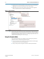
1
Internal Memory (RAM and ROM) User Guide
Internal Memory (RAM and ROM)
User Guide
101 Innovation Drive
San Jose, CA 95134
www.altera.com
UG-01068-5.0
Feedback Subscribe
© 2014 Altera Corporation. All rights reserved. ALTERA, ARRIA, CYCLONE, HARDCOPY, MAX, MEGACORE, NIOS, QUARTUS and STRATIX words and logos
are trademarks of Altera Corporation and registered in the U.S. Patent and Trademark Office and in other countries. All other words and logos identified as
trademarks or service marks are the property of their respective holders as described at www.altera.com/common/legal.html. Altera warrants performance of its
semiconductor products to current specifications in accordance with Altera's standard warranty, but reserves the right to make changes to any products and
services at any time without notice. Altera assumes no responsibility or liability arising out of the application or use of any information, product, or service
described herein except as expressly agreed to in writing by Altera. Altera customers are advised to obtain the latest version of device specifications before relying
on any published information and before placing orders for products or services.
June 2014
Altera Corporation
ISO
9001:2008
Registered
Internal Memory (RAM and ROM)
User Guide
1. About Internal Memory Blocks
This user guide describes the Altera megafunction IP cores that implement the
following memory modes:
■
RAM:1-Port—Single-port RAM
■
RAM:2-Port—Dual-port RAM
■
ROM:1-Port—Single-port ROM
■
ROM:2-Port—Dual-port ROM
Altera provides two IP cores to implement the memory modes—the ALTSYNCRAM
and ALTDPRAM IP cores. The Quartus® II software automatically selects one of these
IP cores to implement memory modes. The selection depends on the target device,
memory modes, and features of the RAM and ROM.
f For more information about IP cores, refer to the Introduction to Altera IP cores.
Features
The internal memory blocks provide the following features:
June 2014
■
“Memory Modes Configuration”
■
“Memory Block Types”
■
“Write and Read Operations Triggering”
■
“Port Width Configuration”
■
“Mixed-width Port Configuration”
■
“Maximum Block Depth Configuration”
■
“Clocking Modes and Clock Enable”
■
“Address Clock Enable”
■
“Byte Enable”
■
“Asynchronous Clear”
■
“Read Enable”
■
“Read-During-Write”
■
“Power-Up Conditions and Memory Initialization”
■
“Error Correction Code”
Altera Corporation
Internal Memory (RAM and ROM)
User Guide
1–2
Internal Memory (RAM and ROM)
User Guide
Chapter 1: About Internal Memory Blocks
Features
June 2014
Altera Corporation
2. Customizing Internal Memory IP Cores
Installing and Licensing IP Cores
The Quartus II software includes the Altera IP Library. The library provides many
useful IP core functions for production use without additional license. You can fully
evaluate any licensed Altera IP core in simulation and in hardware until you are
satisfied with its functionality and performance.
Some Altera IP cores, such as MegaCore® functions, require that you purchase a
separate license for production use. After you purchase a license, visit the Self Service
Licensing Center to obtain a license number for any Altera product. For additional
information, refer to Altera Software Installation and Licensing.
Figure 2–1. IP core Installation Path
acds
quartus - Contains the Quartus II software
ip - Contains the Altera IP Library and third-party IP cores
altera - Contains the Altera IP Library source code
<IP core name> - Contains the IP core source files
1
The default installation directory on Windows is <drive>:\altera\<version number>;
on Linux it is <home directory>/altera/<version number>.
IP Catalog and Parameter Editor
The Quartus II IP Catalog (Tools > IP Catalog) and parameter editor help you easily
customize and integrate IP cores into your project. You can use the IP Catalog and
parameter editor to select, customize, and generate files representing your custom IP
variation.
The IP Catalog automatically displays the IP cores available for your target device.
Double-click any IP core name to launch the parameter editor and generate files
representing your IP variation. The parameter editor prompts you to specify your IP
variation name, optional ports, architecture features, and output file generation
options. The parameter editor generates a top-level .qsys or .qip file representing the
IP core in your project. Alternatively, you can define an IP variation without an open
Quartus II project. When no project is open, select the Device Family directly in IP
Catalog to filter IP cores by device.
1
The IP Catalog is also available in Qsys (View > IP Catalog). The Qsys IP Catalog
includes exclusive system interconnect, video and image processing, and other
system-level IP that are not available in the Quartus II IP Catalog.
Use the following features to help you quickly locate and select an IP core:
■
June 2014
Altera Corporation
Filter IP Catalog to Show IP for active device family or Show IP for all device
families.
Internal Memory (RAM and ROM)
User Guide
2–2
Chapter 2: Customizing Internal Memory IP Cores
■
Search to locate any full or partial IP core name in IP Catalog. Click Search for
Partner IP, to access partner IP information on the Altera website.
■
Right-click an IP core name in IP Catalog to display details about supported
devices, installation location, and links to documentation.
Figure 2–2. Quartus II IP Catalog
Search and filter IP for your target device
Double-click to customize, right-click for information
1
The IP Catalog and parameter editor replace the MegaWizard™ Plug-In Manager in
the Quartus II software. The Quartus II software may generate messages that refer to
the MegaWizard Plug-In Manager. Substitute “IP Catalog and parameter editor” for
“MegaWizard Plug-In Manager” in these messages.
Using the Parameter Editor
The parameter editor helps you to configure your IP variation ports, parameters,
architecture features, and output file generation options:
■
Use preset settings in the parameter editor (where provided) to instantly apply
preset parameter values for specific applications.
■
View port and parameter descriptions and links to detailed documentation.
Internal Memory (RAM and ROM)
User Guide
June 2014
Altera Corporation
Chapter 2: Customizing Internal Memory IP Cores
■
2–3
Generate testbench systems or example designs (where provided).
Figure 2–3. IP Parameter Editors
View IP port
and parameter
details
Legacy parameter
editors
Specify your IP variation name
and target device
Apply preset parameters for
specific applications
Customizing and Generating IP Cores
You can customize IP cores to support a wide variety of applications. The Quartus II
IP Catalog displays IP cores available for the current target device. The parameter
editor guides you to set parameter values for optional ports, features, and output files.
To customize and generate a custom IP core variation, follow these steps:
1. In the IP Catalog (Tools > IP Catalog), locate and double-click the name of the IP
core to customize. The parameter editor appears.
2. Specify a top-level name for your custom IP variation. This name identifies the IP
core variation files in your project. If prompted, also specify the target Altera
device family and output file HDL preference. Click OK.
3. Specify the desired parameters, output, and options for your IP core variation:
■
Optionally select preset parameter values. Presets specify all initial parameter
values for specific applications (where provided).
■
Specify parameters defining the IP core functionality, port configuration, and
device-specific features.
■
Specify options for generation of a timing netlist, simulation model, testbench,
or example design (where applicable).
■
Specify options for processing the IP core files in other EDA tools.
4. Click Finish or Generate to generate synthesis and other optional files matching
your IP variation specifications. The parameter editor generates the top-level .qip
or .qsys IP variation file and HDL files for synthesis and simulation. Some IP cores
also simultaneously generate a testbench or example design for hardware testing.
June 2014
Altera Corporation
Internal Memory (RAM and ROM)
User Guide
2–4
Chapter 2: Customizing Internal Memory IP Cores
When you generate the IP variation with a Quartus II project open, the parameter
editor automatically adds the IP variation to the project. Alternatively, click Project >
Add/Remove Files in Project to manually add a top-level .qip or .qsys IP variation
file to a Quartus II project. To fully integrate the IP into the design, make appropriate
pin assignments to connect ports. You can define a virtual pin to avoid making
specific pin assignments to top-level signals.
Upgrading Outdated IP Cores
Altera IP cores have a version number that corresponds with the Quartus II software
version. The Quartus II software alerts you when your IP core is outdated with
respect to the current Quartus II software version. Click Project > Upgrade IP
Components to easily identify and upgrade outdated IP cores.
You are prompted to upgrade IP when the new version includes port, parameter, or
feature changes. You are also notified if IP is unsupported or cannot be migrated in
the current software. Most Altera IP cores support automatic simultaneous upgrade,
as indicated in the GUI. IP cores unsupported by auto upgrade require regeneration in
the parameter editor.
To upgrade outdated IP cores in your design, follow these steps:
1. In the latest version of the Quartus II software, open the Quartus II project
containing an outdated IP core variation.
2. Click Project > Upgrade IP Components. The Upgrade IP Components dialog
box displays all outdated IP cores in your project, along with basic instructions for
upgrading each core.
3. Upgrading IP cores changes your original design files. To preserve these original
files, click Project > Archive and save a project archive preserving your original
files.
4. To simultaneously upgrade all IP cores that support automatic upgrade, click
Perform Automatic Upgrade. The IP variation upgrades to the latest version.
5. To upgrade IP cores unsupported by automatic upgrade, select the IP core in
Upgrade IP Components dialog box, and then click Upgrade in Editor. The
parameter editor appears. Click Finish or Generate to regenerate the IP variation
and complete the upgrade. The version number updates when complete.
Figure 2–4. Upgrading Outdated IP Cores
Indicates that IP upgrade is:
Required
Optional
Complete
Unsupported
Displays upgrade
status for all IP cores
in the Project
Upgrades all IP core that support “Auto Upgrade”
Upgrades individual IP cores unsupported by “Auto Upgrade”
Internal Memory (RAM and ROM)
User Guide
June 2014
Altera Corporation
Chapter 2: Customizing Internal Memory IP Cores
1
2–5
Altera verifies that the current version of the Quartus II software compiles the
previous version of each IP core. The MegaCore IP Library Release Notes and Errata
reports any verification exceptions. Altera does not verify compilation for IP cores
older than the previous release.
Alternatively, you can upgrade IP cores at the command line. To upgrade a single IP
core:
quartus_sh --ip_upgrade -variation_files <variation_file_path> <project>
To upgrade a list of IP cores:
quartus_sh --ip_upgrade -variation_files
<variation_file_path>;<qsys_file_path>;<variation_file_path> <project>
1
June 2014
Altera Corporation
File paths must be relative to the project directory and you must reference
the IP variation .v or .vhd file or .qsys file, not the .qip file.
Internal Memory (RAM and ROM)
User Guide
2–6
Internal Memory (RAM and ROM)
User Guide
Chapter 2: Customizing Internal Memory IP Cores
June 2014
Altera Corporation
3. Parameter Settings
This section describes the parameter settings for the memory modes.
1
You can use the IP Catalog (Tools > IP Catalog) and parameter editor to define and
generate valid RAM and ROM memory blocks.
Table 3–1 lists the parameter settings for the RAM:1-Port.
Table 3–1. RAM:1-Port Parameter Settings
Option
Legal Values
Default
value
Description
Parameter Settings: Widths/Blk Type/Clks
Specifies the width of the ‘q’ output
bus.
How wide should the ‘q’ output bus be?
—
8
How many <X>-bit words of memory?
—
256
Specifies the number of <X>-bit words.
Auto
Specifies the memory block type. The
types of memory block that are
available for selection depends on your
target device.
What should the memory block type be?
Set the maximum block depth to
Auto, M-RAM, M4K,
M512, M9K, M10K,
M144K, MLAB,
M20K, LCs
Auto, 32, 64, 128,
256, 512, 1024,
2048, 4096,
8192,16384, 32768,
65536
For more information, refer to “Port
Width Configuration” on page 4–7.
For more information refer to “Memory
Block Types” on page 4–4.
Specifies the maximum block depth in
words.
Auto
For more information refer to
“Maximum Block Depth Configuration”
on page 4–9.
Specifies the clocking method to use.
Single clock—A single clock and a
clock enable controls all registers of the
memory block.
Single clock
What clocking method would you like to
use?
or
Dual Clock: use
separate ‘input’ and
‘output’ clocks
Dual Clock: use separate ‘input’ and
‘output’ clocks—An input and an
Single clock output clock controls all registers
related to the data input and output
to/from the memory block including
data, address, byte enables, read
enables, and write enables.
For more information, refer to
“Clocking Modes and Clock Enable” on
page 4–10.
June 2014
Altera Corporation
Internal Memory (RAM and ROM)
User Guide
3–2
Chapter 3: Parameter Settings
Table 3–1. RAM:1-Port Parameter Settings
Default
value
Description
On/Off
On
Specifies whether to register the input
and output ports.
Create one clock enable signal for each
clock signal. Note: All registered ports are
controlled by the enable signal(s)
On/Off
Off
Specifies whether to turn on the option
to create one clock enable signal for
each clock signal.
Use clock enable for
port A input
registers
On/Off
Off
Specifies whether to use clock enable
for port A input registers.
Use clock enable for
port A output
registers
On/Off
Off
Specifies whether to use clock enable
for port A output registers.
Option
Legal Values
Parameter Settings: Regs/Clken/Byte Enable/Aclrs
Which ports should be registered?
The following options are available:
■
‘data’ and ‘wren’ input ports
■
‘address’ input port
■
‘q’ output port
More Options
Create an
‘addressstall_a’
input port.
On/Off
Off
Specifies whether to create a
addressstall_a input port. You can
create this port to act as an extra active
low clock enable input for the address
registers.
For more information, refer to “Address
Clock Enable” on page 4–12.
Create byte enable for port A
On/Off
Off
Specifies whether to create a byte
enable for port A. Turn on this option if
you want to mask the input data so that
only specific bytes, nibbles, or bits of
data are written.
For more information, refer to “Byte
Enable” on page 4–13.
What is the width of a byte for byte
enables?
Create an ‘aclr’ asynchronous clear for the
registered ports.
MLAB: 5 or 10
Other memory block
types: 8 or 9
M10K and M20K: 8,
9, or 10
On/Off
MLAB: 5
Other
memory
block types:
8
Off
Specifies the byte width of the byte
enable port. The width of the data input
port must be divisible by the byte size.
For more information, refer to “Byte
Enable” on page 4–13.
Specifies whether to create an
asynchronous clear port for the
registered data, wren, address, q,
and byteena_a ports.
For more information, refer to
“Asynchronous Clear” on page 4–14.
More Options
‘q’ port
On/Off
Off
Turn on this option for the ‘q’ port to be
affected by the asynchronous clear
signal.
The disabled ports are not affected by
the asynchronous clear signal.
Internal Memory (RAM and ROM)
User Guide
June 2014 Altera Corporation
Chapter 3: Parameter Settings
3–3
Table 3–1. RAM:1-Port Parameter Settings
Option
Legal Values
Create a ‘rden’ read enable signal
On/Off
Default
value
Off
Description
Specifies whether to create a read
enable signal.
For more information, refer to “Read
Enable” on page 4–15.
Parameter Settings: Read During Write Option
Specifies the output behavior when
read-during-write occurs.
What should the q output be when reading
from a memory location being written to?
New data, Don’t
Care
New data
New Data—New data is available on
the rising edge of the same clock cycle
on which it was written.
Don’t Care—The RAM outputs “don't
care” or “unknown” values for
read-during-write operation.
For more information, refer to “ReadDuring-Write” on page 4–16.
Turn on this option to obtain ‘X’ on the
masked byte.
Get x’s for write masked bytes instead of
old data when byte enable is used
On/Off
On
For M10K and M20K memory block,
this option is not available if you
specify New Data as the output
behavior when RDW occurs.
Parameter Settings: Mem Init
Specifies the initial content of the
memory.
To initialize the memory to zero, select
No, leave it blank.
No, leave it blank
Do you want to specify the initial content
of the memory?
or
Yes, use this file for
the memory content
data
No, leave it
blank
To use a memory initialization file
(.mif) or a hexadecimal (Intel-format)
file (.hex), select Yes, use this file for
the memory content data.
For more information, refer to “PowerUp Conditions and Memory
Initialization” on page 4–18.
Allow In-System Memory Content Editor to
capture and update content independently
of the system clock
The ‘Instance ID’ of this RAM is
June 2014
Altera Corporation
On/Off
Off
—
None
Specifies whether to allow In-System
Memory Content Editor to capture and
update content independently of the
system clock.
Specifies the RAM ID.
Internal Memory (RAM and ROM)
User Guide
3–4
Chapter 3: Parameter Settings
Table 3–2 lists the parameter settings for the RAM:2-Port.
Table 3–2. RAM:2-Port Parameter Settings
Option
Legal Values
Default
values
Description
Parameter Settings: General
With one read port and
one write port
How will you be using the dual port RAM?
With one
read port
and one
write port
Specifies how you use the dual
port RAM.
Determines whether to specify
the memory size in words or bits.
As a number of bits
As a
number of
words
—
256
Specifies the number of <X>-bit
words.
On/Off
Off
Specifies whether to use different
data widths on different ports.
or
With two read /write
ports
As a number of words
How do you want to specify the memory size?
or
Parameter Settings: Widths/ Blk Type
How many <X>-bit words of memory?
Use different data widths on different ports
When you select With one read port and one
write port, the following options are available:
■
How wide should the ‘q_a’ output bus be?
■
How wide should the ‘data_a’ input bus be?
■
How wide should the ‘q’ output bus be?
Specifies the width of the input
and output ports.
—
8
When you select With two read/write ports,
the following options are available:
■
How wide should the ‘q_a’ output bus be?
■
How wide should the ‘q_b’ output bus be?
What should the memory block type be?
Auto, M-RAM, M4K,
M512, M9K, M10K,
M144K, MLAB, M20K,
LCs
Use default logic cell
style
How should the memory be implemented?
or
Use Stratix M512
emulation logic cell
style
Internal Memory (RAM and ROM)
User Guide
Auto
For more information, refer to
“Port Width Configuration” on
page 4–7.
Specifies the memory block type.
The types of memory block that
are available for selection
depends on your target device.
For more information refer to
“Memory Block Types” on
page 4–4.
Use
default
logic cell
style
Specifies the logic cell
implementation options. This
option is enabled only when you
choose LCs memory type.
June 2014 Altera Corporation
Chapter 3: Parameter Settings
3–5
Table 3–2. RAM:2-Port Parameter Settings
Option
Set the maximum block depth to
Legal Values
Auto, 32, 64, 128, 256,
512, 1024, 2048, 4096
Default
values
Auto
Description
Specifies the maximum block
depth in words. This option is
enabled only when you set the
memory block type to Auto.
For more information refer to
“Maximum Block Depth
Configuration” on page 4–9.
Parameter Settings: Clks/Rd, Byte En
Specifies the clocking method to
use.
Single clock—A single clock and
a clock enable controls all
registers of the memory block.
When you select With
one read port and one
write port, the following
values are available:
What clocking method would you like to use?
■
Single clock
■
Dual clock: use
separate ‘input’ and
‘output’ clocks
■
Dual clock: use
separate ‘read’ and
‘write’ clock
When you select With
two read/write ports, the
following options are
available:
■
Single clock
■
Dual clock: use
separate ‘input’ and
‘output’ clocks
■
Dual clock: use
separate clocks for A
and B ports
Dual Clock: use separate ‘input’
and ‘output’ clocks—An input
and an output clock controls all
registers related to the data input
and output to/from the memory
block including data, address,
byte enables, read enables, and
write enables.
Single
clock
Dual clock: use separate ‘read’
and ‘write’ clock—A write clock
controls the data-input, writeaddress, and write-enable
registers while the read clock
controls the data-output, readaddress, and read-enable
registers.
Dual clock: use separate clocks
for A and B ports—Clock A
controls all registers on the port
A side; clock B controls all
registers on the port B side. Each
port also supports independent
clock enables for both port A and
port B registers, respectively.
For more information, refer to
“Clocking Modes and Clock
Enable” on page 4–10.
June 2014
Altera Corporation
Internal Memory (RAM and ROM)
User Guide
3–6
Chapter 3: Parameter Settings
Table 3–2. RAM:2-Port Parameter Settings
Option
Legal Values
Default
values
Specifies whether to create a
read enable signal for port B.
When you select With one read port and one
write port, the following option is available:
For more information, refer to
“Read Enable” on page 4–15.
Create a ‘rden’ read enable signal
When you select With two read/write ports,
the following option is available:
—
Off
Create a ‘rden_a’ and ‘rden_b’ read enable
signal
Specifies whether to create a
read enable signal for port A and
B.
For more information, refer to
“Read Enable” on page 4–15.
Create byte enable for port A
Create byte enable for port B
Description
Specifies whether to create a
byte enable for port A and B.
Turn on these options if you want
to mask the input data so that
only specific bytes, nibbles, or
bits of data are written.
—
Off
The option to create a byte
enable for port B is only available
when you select two read/write
ports.
For more information, refer to
“Byte Enable” on page 4–13.
Enable error checking and correcting (ECC) to
check and correct single bit errors and detect
double errors
Specifies whether to enable the
ECC feature that corrects single
bit errors and detects double
errors at the output of the
memory.
On/Off
Off
This option is only available in
devices that support M144K
memory block type.
For more information, refer to
“Error Correction Code” on
page 4–19.
Enable error checking and correcting (ECC) to
check and correct single bit errors, double
adjacent bit errors, and detect triple adjacent
bit errors
Specifies whether to enable the
ECC feature that corrects single
bit errors, double adjacent bit
errors, and detects triple
adjacent bit errors at the output
of the memory.
On/Off
Off
This option is only available in
devices that support M20K
memory block type.
For more information, refer to
“Error Correction Code” on
page 4–19.
Internal Memory (RAM and ROM)
User Guide
June 2014 Altera Corporation
Chapter 3: Parameter Settings
3–7
Table 3–2. RAM:2-Port Parameter Settings
Option
Legal Values
Default
values
Description
On/Off
On
Specifies whether to register the
read or write input and output
ports.
On
The read and write input ports
are turned on by default. You
only need to specify whether to
register the Q output ports.
Parameter Settings: Regs/Clkens/Aclrs
Which ports should be registered?
When you select With one read port and one
write port, the following options are available:
■
‘data’, ‘wraddress’, and ‘wren’ write input
ports
■
‘raddress’ and ‘rden’ read input port
■
Read output port(s) ‘q’
When you select With two read/write ports,
the following options are available:
■
‘data_a’, ‘wraddress_a’, and ‘wren_a’ write
input ports
■
Read output port(s) ‘q’_a and ‘q_b’
When you select
With one read port
and one write port,
the following
options are
available:
More Options
June 2014
Altera Corporation
■
‘data’ port
■
‘wraddress’ port
■
‘wren’ port
■
‘raddress’ port
■
‘q_b’ port
When you select
With two read
/write ports, the
following options
are available:
■
‘data_a’ port
■
‘data_b’ port
■
‘wraddress_a’
port
■
‘wraddress_b’
port
■
‘wren_a’ port
■
‘wren_b’ port
■
‘q_a’ port
■
‘q_b’ port
On/Off
Internal Memory (RAM and ROM)
User Guide
3–8
Chapter 3: Parameter Settings
Table 3–2. RAM:2-Port Parameter Settings
Option
Legal Values
Create one clock enable signal for each clock
signal.
On/Off
Default
values
Off
Description
Specifies whether to turn on the
option to create one clock enable
signal for each clock signal.
For more information, refer to
“Clocking Modes and Clock
Enable” on page 4–10.
When you select
With one read port
and one write port,
the following
option is available:
Use clock enable
for write input
registers
More Options
When you select
With two read
/write ports, the
following options
are available:
■
Use clock
enable for port A
input registers
■
Use clock
enable for port B
input registers
■
Use clock
enable for port A
output registers
■
Use clock
enable for port B
output register
Internal Memory (RAM and ROM)
User Guide
On/Off
Off
Clock enable for port B input and
output registers are turned on by
default. You only need to specify
whether to use clock enable for
port A input and output registers.
For more information, refer to
“Clocking Modes and Clock
Enable” on page 4–10
June 2014 Altera Corporation
Chapter 3: Parameter Settings
3–9
Table 3–2. RAM:2-Port Parameter Settings
Option
Legal Values
Default
values
Description
When you select
With one read port
and one write port,
the following
options are
available:
■
■
More Options
Create an
‘wr_addressstall
’ input port.
Create an
‘rd_addressstall’
input port.
On/Off
Off
When you select
With two read
/write ports, the
following options
are available:
■
Create an
‘addressstall_a’
input port.
■
Create an
‘addressstall_b’
input port.
Create an ‘aclr’ asynchronous clear for the
registered ports.
Specifies whether to create clock
enables for address registers.
You can create these ports to act
as an extra active low clock
enable input for the address
registers.
For more information, refer to
“Address Clock Enable” on
page 4–12.
On/Off
Off
On/Off
Off
Specifies whether to create an
asynchronous clear port for the
registered ports.
For more information, refer to
“Asynchronous Clear” on
page 4–14.
When you select
With one read port
and one write port,
the following
options are
available:
More Options
■
‘rdaddress’ port
■
‘q_b’ port
When you select
With two read
/write ports, the
following options
are available:
June 2014
Altera Corporation
■
‘q_a’ port
■
‘q_b’ port
Specifies whether the ‘raddress’,
‘q_a’, and ‘q_b’ ports are cleared
by the aclr port.
Internal Memory (RAM and ROM)
User Guide
3–10
Chapter 3: Parameter Settings
Table 3–2. RAM:2-Port Parameter Settings
Option
Legal Values
Default
values
Description
Parameter Settings: Output 1
Specifies the output behavior
when read-during-write occurs.
Old memory contents appear—
The RAM outputs reflect the old
data at that address before the
write operation proceeds.
I do not care—This option
functions differently when you
turn it on depending on the
following memory block type you
select:
When you select With one read port and one
write port, the following option is available:
How should the q output behave when reading
a memory location that is being written from
the other port?
When you select With two read /write ports,
the following option is available:
Old memory contents
appear
or
■
When you set the memory
block type to Auto, M144K,
M512, M4K, M9K, M10K,
M20K or any other block
RAM, the RAM outputs ‘don't
care’ or “unknown” values for
read-during-write operation
without analyzing the timing
path.
■
When you set the memory
block type to MLAB (for
LUTRAM), the RAM outputs
‘dont care’ or ‘unknown’
values for read-during-write
operation but analyzes the
timing path to prevent
metastability.
I do not
care
I do not care
How should the q_a and q_b outputs behave
when reading a memory location that is being
written from the other port?
For more information, refer to
“Read-During-Write” on
page 4–16.
Do not analyze the timing between write and
read operation. Metastability issues are
prevented by never writing and reading at the
same address at the same time.
Internal Memory (RAM and ROM)
User Guide
On/Off
Off
Turn on this option when you
want the RAM to output ‘don’t
care’ or unknown values for
read-during-write operation
without analyzing the timing
path.
This option is only available for
LUTRAM and is enabled when
you set memory block type to
MLAB.
June 2014 Altera Corporation
Chapter 3: Parameter Settings
3–11
Table 3–2. RAM:2-Port Parameter Settings
Option
Legal Values
Default
values
Description
Parameter Settings: Output 2 (This tab is only available when you select two read/ write ports)
What should the ‘q_a’ output be when reading
from a memory location being written to?
Specifies the output behavior
when read-during-write occurs.
New Data—New data is available
on the rising edge of the same
clock cycle on which it was
written.
What should the ‘q_b’ output be when reading
from a memory location being written to?
New data, Old Data
New data
Old Data—The RAM outputs
reflect the old data at that
address before the write
operation proceeds.
For more information, refer to
“Read-During-Write” on
page 4–16.
Get x’s for write masked bytes instead of old
data when byte enable is used
On/Off
On
Turn on this option to obtain ‘X’
on the masked byte.
Parameter Settings: Mem Init
Specifies the initial content of the
memory.
To initialize the memory to zero,
select No, leave it blank.
No, leave it blank
Do you want to specify the initial content of
the memory?
or
Yes, use this file for the
memory content data
No, leave
it blank
To use a memory initialization file
(.mif) or a hexadecimal
(Intel-format) file (.hex), select
Yes, use this file for the
memory content data.
For more information, refer to
“Power-Up Conditions and
Memory Initialization” on
page 4–18.
June 2014
Altera Corporation
Internal Memory (RAM and ROM)
User Guide
3–12
Chapter 3: Parameter Settings
Table 3–3 lists the parameter settings for the ROM:1-Port.
Table 3–3. ROM:1-Port Parameter Settings
Option
Legal Values
Default
values
Description
Parameter Settings: General Page
Specifies the width of the ‘q’
output bus.
How wide should the ‘q’ output bus be?
—
8
How many <X>-bit words of memory?
—
256
What should the memory block type be?
Auto, M4K, M9K,
M144K, M10K, M20K
Auto
For more information, refer to
“Port Width Configuration” on
page 4–7.
Specifies the number of <X>-bit
words.
Specifies the memory block
type. The types of memory
block that are available for
selection depends on your
target device.
For more information, refer to
“Memory Block Types” on
page 4–4.
Set the maximum block depth to
Auto, 32, 64, 128,
256, 512, 1024,
2048, 4096
Specifies the maximum block
depth in words.
Auto
For more information, refer to
“Maximum Block Depth
Configuration” on page 4–9
Specifies the clocking method
to use.
Single clock—A single clock
and a clock enable controls all
registers of the memory block
Single clock
or
What clocking method would you like to use?
Dual clock: use
separate ‘input’ and
‘output’ clocks
Dual clock (Input and Output
clock)—The input clock
Single clock controls the address registers
and the output clock controls
the data-out registers. There are
no write-enable, byte-enable, or
data-in registers in ROM mode.
For more information, refer to
“Clocking Modes and Clock
Enable” on page 4–10.
Parameter Settings: Regs/Clken/Aclrs
Which ports should be registered?
‘q’ output port
Create one clock enable signal for each clock
signal. Note: All registered ports are controlled
by the enable signal(s)
Internal Memory (RAM and ROM)
User Guide
On/Off
On/Off
On
Specifies whether to register the
‘q’ output port.
Off
Specifies whether to turn on the
option to create one clock
enable signal for each clock
signal.
June 2014 Altera Corporation
Chapter 3: Parameter Settings
3–13
Table 3–3. ROM:1-Port Parameter Settings
Legal Values
Default
values
Description
Use clock enable for
port A input
registers
On/Off
Off
Specifies whether to use clock
enable for port A input registers.
Use clock enable for
port A output
registers
On/Off
Off
Specifies whether to use clock
enable for port A output
registers.
Option
More Options
Create an
‘addressstall_a’
input port.
On/Off
Off
Specifies whether to create a
addressstall_a input port.
You can create this port to act
as an extra active low clock
enable input for the address
registers.
For more information, refer to
“Address Clock Enable” on
page 4–12.
Create an ‘aclr’ asynchronous clear for the
registered ports.
Specifies whether to create an
asynchronous clear port for the
registered ports.
On/Off
Off
‘address’ port
On/Off
Off
Specifies whether the ‘address’
port should be affected by the
‘aclr’ port.
‘q’ port
On/Off
Off
Specifies whether the ‘q’ port
should be affected by the ‘aclr’
port.
More Options
Create a ‘rden’ read enable signal
On/Off
Off
For more information, refer to
“Asynchronous Clear” on
page 4–14.
Specifies whether to create a
read enable signal.
For more information, refer to
“Read Enable” on page 4–15.
Parameter Settings: Mem Init
Specifies the initial content of
the memory.
Do you want to specify the initial content of the
memory?
Yes, use this file for
the memory content
data
In ROM mode you must specify
a memory initialization file
(.mif) or a hexadecimal
Yes, use
(Intel-format) file (.hex). The
this file for
Yes, use this file for the
the memory
memory content data option is
content data
turned on by default.
For more information, refer to
“Power-Up Conditions and
Memory Initialization” on
page 4–18.
June 2014
Altera Corporation
Internal Memory (RAM and ROM)
User Guide
3–14
Chapter 3: Parameter Settings
Table 3–3. ROM:1-Port Parameter Settings
Option
Allow In-System Memory Content Editor to
capture and update content independently of the
system clock
The ‘Instance ID’ of this ROM is
Legal Values
Default
values
On/Off
Off
—
None
Description
Specifies whether to allow
In-System Memory Content
Editor to capture and update
content independently of the
system clock
Specifies the ROM ID.
Table 3–4 lists the parameter settings for the ROM:2-Port.
Table 3–4. ROM:2-Port Parameter Settings
Option
Legal Values
Default
values
Description
Parameter Settings: Widths/Blk Type
As a number of words
How do you want to specify the memory size?
or
As a number
of words
Determines whether to specify
the memory size in words or
bits.
256
Specifies the number of <X>-bit
words.
As a number of bits
How many <X>-bit words of memory?
Use different data widths on different ports
32, 64, 128, 256,
512, 1024, 2048,
4096, 8192, 16384,
32768, 65536
On/Off
Off
How wide should the ‘q_a’ output bus be?
How wide should the ‘q_b’ output bus be?
What should the memory block type be?
Set the maximum block depth to
Internal Memory (RAM and ROM)
User Guide
Specifies whether to use
different data widths on different
ports.
For more information, refer to
“Mixed-width Port
Configuration” on page 4–8.
Specifies the width of the ‘q_a’
and ‘q_b’ output ports.
—
Auto, M4K, M9K,
M144K, M10K,
M20K, MLAB
Auto, 128, 256, 512,
1024, 2048, 4096
8
Auto
For more information, refer to
“Port Width Configuration” on
page 4–7.
Specifies the memory block
type. The types of memory block
that are available for selection
depends on your target device
For more information, refer to
“Memory Block Types” on
page 4–4.
Auto
Specifies the maximum block
depth in words. This option is
enabled only when you choose
Auto as the memory block type.
For more information, refer to
“Maximum Block Depth
Configuration” on page 4–9.
June 2014 Altera Corporation
Chapter 3: Parameter Settings
3–15
Table 3–4. ROM:2-Port Parameter Settings
Option
Legal Values
Default
values
Description
Parameter Settings: Clks/Rd, Byte En
Specifies the clocking method to
use.
Single clock—A single clock
and a clock enable controls all
registers of the memory block
Single clock
or
What clocking method would you like to use?
Dual Clock: use
separate ‘input’ and
‘output’ clocks
Dual Clock: use separate ‘input’
and ‘output’ clocks—The input
clock controls the address
registers and the output clock
controls the data-out registers.
There are no write-enable,
byte-enable, or data-in registers
Single clock in ROM mode.
or
Dual clock: use separate clocks
for A and B ports—Clock A
controls all registers on the port
A side; clock B controls all
registers on the port B side.
Each port also supports
independent clock enables for
both port A and port B registers,
respectively.
Dual clock: use
separate clocks for A
and B ports
For more information, refer to
“Clocking Modes and Clock
Enable” on page 4–10.
Create a ‘rden_a’ and ‘rden_b’ read enable
signals
Specifies whether to create read
enable signals.
—
Off
On/Off
On
Specifies whether to register the
‘q_a’ and ‘q_b’ output ports.
‘q_a’ port
On/Off
On
Specifies whether to register the
‘q_a’ output port.
‘q_b’ port
On/Off
On
Specifies whether to register the
‘q_b’ output port.
On/Off
Off
Specifies whether to turn on the
option to create one clock enable
signal for each clock signal.
For more information, refer to
“Read Enable” on page 4–15.
Parameter Settings: Regs/Clkens/Aclrs
Read output port(s) ‘q_a’ and ‘q_b’
More Options
Create one clock enable signal for each clock
signal.
June 2014
Altera Corporation
Internal Memory (RAM and ROM)
User Guide
3–16
Chapter 3: Parameter Settings
Table 3–4. ROM:2-Port Parameter Settings
Legal Values
Default
values
Description
Use clock enable for
port A input registers
On/Off
Off
Specifies whether to use clock
enable for port A input registers.
Use clock enable for
port A output
registers
On/Off
Off
Specifies whether to use clock
enable for port A output
registers.
Option
More Options
Create an
‘addressstall_a’ input
port.
Create an
‘addressstall_b’
input port.
On/Off
Off
Specifies whether to create
addressstall_a and
addressstall_b input ports.
You can create these ports to act
as an extra active low clock
enable input for the address
registers.
For more information, refer to
“Address Clock Enable” on
page 4–12.
Specifies whether to create an
asynchronous clear port for the
registered ports.
Create an ‘aclr’ asynchronous clear for the
registered ports.
On/Off
Off
‘q_a’ port
On/Off
Off
Specifies whether the ‘q_a’ port
should be cleared by the aclr
port.
‘q_b’ port
On/Off
Off
Specifies whether the ‘q_b’ port
should be cleared by the aclr
port.
More Options
For more information, refer to
“Asynchronous Clear” on
page 4–14.
Parameter Settings: Mem Init
Specifies the initial content of
the memory.
Do you want to specify the initial content of the
memory?
Yes, use this file for
the memory content
data
In ROM mode you must specify
a memory initialization file (.mif)
Yes, use
or a hexadecimal (Intel-format)
this file for file (.hex). The Yes, use this file
the memory for the memory content data
content data option is turned on by default.
For more information, refer to
“Power-Up Conditions and
Memory Initialization” on
page 4–18.
PORT_A
The initial content file should conform to which
port’s dimensions?
or
PORT_B
Internal Memory (RAM and ROM)
User Guide
PORT_A
Specifies whether the initial
content file conforms to port A
or port B.
June 2014 Altera Corporation
4. Functional Description
This section describes the features and functionality of the internal memory blocks
and the ports of the ALTSYNCRAM and ALTDPRAM IP cores.
Memory Modes Configuration
A memory block contains two address ports (port A and port B) with their respective
output data ports, and you can use them for read and write operations depending on
the memory mode you choose. The input and output ports shown in the block
diagrams refer to the ports of the wrapper that contains the memory IP core
instantiated in it. The ports of the wrapper are mapped to the ports of either the
ALTSYNCRAM or the ALTDPRAM IP core depending on your memory
configuration, and the port name reflects the memory features you create. For
example, the name of the wrapper port clockena maps to the clock_enable_input_a
port of the ALTSYNCRAM IP core, which relates to the clock enable feature.
For more information about the ports of the ALTSYNCRAM and ALTDPRAM IP
cores, refer to “ALTSYNCRAM and ALTDPRAM Ports” on page 4–20.
Single-port RAM
In a single-port RAM, the read and write operations share the same address at port A,
and the data is read from output port A.
Figure 4–1 shows a block diagram of a typical single-port RAM.
Figure 4–1. Single-port RAM
data[]
address[]
wren
byteena[]
addressstall
inclock
q[]
outclock
clockena
rden
aclr
June 2014
Altera Corporation
Internal Memory (RAM and ROM)
User Guide
4–2
Chapter 4: Functional Description
Memory Modes Configuration
Simple Dual-port RAM
In simple dual-port RAM mode, a dedicated address port is available for each read
and write operation (one read port and one write port). A write operation uses write
address from port A while read operation uses read address and output from port B.
Figure 4–2 shows the block diagram of a simple dual-port RAM.
Figure 4–2. Simple Dual-Port RAM
data[]
wraddress[]
rdaddress[]
rden
wren
byteena[]
wr_addressstall
wrclock
wrclocken
q[]
rd_addressstall
rdclock
rdclocken
ecc_status[]
aclr
True Dual-port RAM
In true dual-port RAM mode, two address ports are available for read or write
operation (two read/write ports). In this mode, you can write to or read from the
address of port A or port B, and the data read is shown at the output port with respect
to the read address port.
Figure 4–3 shows the block diagrams of a true dual-port RAM.
Figure 4–3. True Dual-port RAM
data_a[]
address_a[]
wren_a
byteena_a[]
addressstall_a
clock_a
rden_a
Internal Memory (RAM and ROM)
User Guide
data_b[]
address_b[]
wren_b
byteena_b[]
addressstall_b
clock_b
rden_b
aclr_a
aclr_b
q_a[]
q_b[]
June 2014 Altera Corporation
Chapter 4: Functional Description
Memory Modes Configuration
4–3
Single-port ROM
In single-port ROM, only one address port is available for read operation.
Figure 4–4 shows the block diagram of a single-port ROM.
Figure 4–4. Single-port ROM
address[]
addressstall_a
inclock
inclocken
outclock
outclocken
q[]
outaclr
Dual-port ROM
The dual-port ROM has almost similar functional ports as single-port ROM. The
difference is dual-port ROM has an additional address port for read operation.
Figure 4–5 shows the block diagram of a dual-port ROM.
Figure 4–5. Dual-port ROM
address_a[]
outclock
address_b[]
outclocken
addressstall_a
addressstall_b
q_a[]
inclock
q_b[]
aclr_b
inclocken
aclr_a
June 2014
Altera Corporation
Internal Memory (RAM and ROM)
User Guide
4–4
Chapter 4: Functional Description
Memory Block Types
Memory Block Types
Altera provides various sizes of embedded memory blocks for various devices. The
parameter editor allows you to implement your memory in the following ways:
■
Select the type of memory blocks available based on your target device. Refer to
Table 4–1 on page 4–5. To select the appropriate memory block type for your
device, obtain more information about the features of your selected internal
memory block in your target device, such as the maximum performance,
supported configurations (depth × width), byte enable, power-up condition, and
the write and read operation triggering.
■
Use logic cells. As compared to internal memory resources, using logic cells to
create memory reduces the design performance and utilizes more area. This
implementation is normally used when you have used up all the internal memory
resources. When logic cells are used, the parameter editor provides you with the
following two types of logic cell implementations:
■
■
Default logic cell style—the write operation triggers (internally) on the rising
edge of the write clock and have continuous read. This implementation uses
less logic cells and is faster, but it is not fully compatible with the Stratix M512
emulation style.
■
Stratix M512 emulation logic cell style—the write operation triggers
(internally) on the falling edge of the write clock and performs read only on the
rising edge of the read clock.
Select the Auto option, which allows the software to automatically select the
appropriate internal memory resource. When you set the memory block type to
Auto, the compiler favors larger block types that can support the memory capacity
you require in a single internal memory block. This setting gives the best
performance and requires no logic elements (LEs) for glue logic. When you create
the memory with specific internal memory blocks, such as M9K, the compiler is
still able to emulate wider and deeper memories than the block type supported
natively. The compiler spans multiple internal memory blocks (only of the same
type) with glue logic added in the LEs as needed.
1
Internal Memory (RAM and ROM)
User Guide
To obtain proper implementation based on the memory configuration you
set, allow the Quartus II software to automatically choose the memory type.
This gives the compiler the flexibility to place the memory function in any
available memory resources based on the functionality and size.
June 2014 Altera Corporation
Chapter 4: Functional Description
Memory Block Types
4–5
Table 4–1 lists the options available for you to implement your memory blocks in
various device families.
Table 4–1. Internal Memory Blocks in Altera Devices
Memory Block Types
M512 (1)
(512 bits)
M4K
(4 Kbits)
M-RAM (2)
(512 Kbits)
MLAB(640
bits)
M9K
(9 Kbits)
M144K
(144 Kbits)
M10K
(10 Kbits)
M20K
(20 Kbits)
Logic
Cell
(LC)
Arria II GX
—
—
—
v
v
—
—
—
v
Arria II GZ
—
—
—
v
v
v
—
—
v
Arria V
—
—
—
v
—
—
v
—
v
Cyclone IV
—
—
—
—
v
—
—
—
v
Cyclone V
—
—
—
v
—
—
v
—
v
Max II
—
—
—
—
—
—
—
—
v
Stratix IV
—
—
—
v
v
v
—
—
v
Stratix V
—
—
—
v
—
—
—
v
v
Device Family
Notes to Table 4–1:
(1) M512 blocks are not supported in true dual-port RAM mode, and dual-port ROM mode
(2) M-RAM blocks are not supported in ROM mode.
(3) MLAB blocks are not supported in simple dual-port RAM mode with mixed-width port feature, true dual-port RAM mode, and dual-port ROM mode.
1
To identify the type of memory block that the software selects to create your memory,
refer to the fitter report after compilation.
f For more information about internal memory blocks and the specifications, refer to
the memory related chapters in your target device handbook.
June 2014
Altera Corporation
Internal Memory (RAM and ROM)
User Guide
4–6
Chapter 4: Functional Description
Write and Read Operations Triggering
Write and Read Operations Triggering
The internal memory blocks vary slightly in its supported features and behaviors.
One important variation is the difference in the write and read operations triggering.
Table 4–2 lists the write and read operations triggering for various internal memory
blocks.
Table 4–2. Write and Read Operations Triggering for internal Memory Blocks
internal Memory Blocks
Write Operation (1)
Read Operation
M10K
Rising clock edges
Rising clock edges
M20K
Rising clock edges
Rising clock edges
M144K
Rising clock edges
Rising clock edges
M9K
Rising clock edges
Rising clock edges
Falling clock edges
MLAB
Rising clock edges (in Arria V, Cyclone V,
and Stratix V devices only)
M-RAM
Rising clock edges
Rising clock edges
(2)
Rising clock edges
M4K
Falling clock edges
Rising clock edges
M512
Falling clock edges
Rising clock edges
Notes to Table 4–2:
(1) Write operation triggering is not applicable to ROMs.
(2) MLAB supports continuos reads. For example, when you write a data at the write clock rising edge and after the
write operation is complete, you see the written data at the output port without the need for a read clock rising edge.
It is important that you understand the write operation triggering to avoid potential
write contentions that can result in unknown data storage at that location.
Internal Memory (RAM and ROM)
User Guide
June 2014 Altera Corporation
Chapter 4: Functional Description
Port Width Configuration
4–7
Figure 4–6 and Figure 4–7 show the valid write operation that triggers at the rising
and falling clock edge, respectively.
Figure 4–6. Valid Write Operation that Triggers at Rising
Clock Edges
Figure 4–7. Valid Write Operation that Triggers at Falling
Clock Edge
clock_a
clock_a
address_a
01
address_a
01
wren_a
wren_a
data_a
data_a
06
05
twc
06
05
Valid Write
twc
Valid Write Actual Write
clock_b
clock_b
address_b
address_b
01
01
wren_b
wren_b
data_b
02
03
04
05
data_b
02
03
04
05
Figure 4–6 assumes that twc is the maximum write cycle time interval. Write operation
of data 03 through port B does not meet the criteria and causes write contention with
the write operation at port A, which result in unknown data at address 01. The write
operation at the next rising edge is valid because it meets the criteria and data 04
replaces the unknown data.
Figure 4–7 assumes that twc is the maximum write cycle time interval. Write operation
of data 04 through port B does not meet the criteria and therefore causes write
contention with the write operation at port A that result in unknown data at address
01. The next data (05) is latched at the next rising clock edge that meets the criteria and
is written into the memory block at the falling clock edge.
1
Data and addresses are latched at the rising edge of the write clock regardless of the
different write operation triggering.
Port Width Configuration
The port width configuration is defined by the following equation:
Memory depth (number of words) × Width of the data input bus
f For more information about the supported port width configuration for various
internal memory blocks, refer to the memory related chapters in your target device
handbook.
June 2014
Altera Corporation
Internal Memory (RAM and ROM)
User Guide
4–8
Chapter 4: Functional Description
Mixed-width Port Configuration
If your port width configuration (either the depth or the width) is more than the
amount an internal memory block can support, additional memory blocks (of the
same type) are used. For example, if you configure your M9K as 512 × 36, which
exceeds the supported port width of 512 × 18, two M9Ks are used to implement your
RAM.
In addition to the supported configuration provided, you can set the memory depth
to a non-power of two, but the actual memory depth allocated can vary. The variation
depends on the type of resource implemented.
If the memory is implemented in dedicated memory blocks, setting a non-power of
two for the memory depth reflects the actual memory depth. If the memory is
implemented in logic cells (and not using Stratix M512 emulation logic cell style that
can be set through the parameter editor), setting a non-power of two for the memory
depth does not reflect the actual memory depth. In this case, you write to or read from
up to 2 address_width memory locations even though the memory depth you set is less
than 2 address_width . For example, if you set the memory depth to 3, and the RAM is
implemented using logic cells, your actual memory depth is 4.
When you implement your memory using dedicated memory blocks, you can check
the actual memory depth by referring to the fitter report.
Mixed-width Port Configuration
Only dual-port RAM and dual-port ROM support mixed-width port configuration for
all memory block types except when they are implemented with LEs. The support for
mixed-width port depends on the width ratio between port A and port B. In addition,
the supporting ratio varies for various memory modes, memory blocks, and target
devices.
1
MLABs do not have native support for mixed-width operation, thus the
option to select MLABs is disabled in the parameter editor. However, the
Quartus II software can implement mixed-width memories in MLABs by
using more than one MLAB. Therefore, if you select AUTO for your
memory block type, it is possible to implement mixed-width port memory
using multiple MLABs.
f For more information about width ratio that supports mixed-width port,
refer to your relevant device handbook.
Memory depth of 1 word is not supported in simple dual-port and true dual-port
RAMs with mixed-width port. The parameter editor prompts an error message when
the memory depth is less than 2 words. For example, if the width for port A is 4 bits
and the width for port B is 8 bits, the smallest depth supported by the RAM is 4
words. This configuration results in memory size of 16 bits (4 × 4) and can be
represented by memory depth of 2 words for port B. If you set the memory depth to 2
words that results in memory size of 8 bits (2 × 4), it can only be represented by
memory depth of 1 word for port B, and therefore the width of the port is not
supported.
Internal Memory (RAM and ROM)
User Guide
June 2014 Altera Corporation
Chapter 4: Functional Description
Maximum Block Depth Configuration
4–9
Maximum Block Depth Configuration
You can limit the maximum block depth of the dedicated memory block you use. The
memory block can be sliced to your desired maximum block depth. For example, the
capacity of an M9K block is 9,216 bits, and the default memory depth is 8K, in which
each address is capable of storing 1 bit (8K × 1). If you set the maximum block depth
to 512, the M9K block is sliced to a depth of 512 and each address is capable of storing
up to 18 bits (512 × 18).
You can use this option to save power usage in your devices. However, this parameter
might increase the number of LEs and affects the design performance.
When the RAM is sliced shallower, the dynamic power usage decreases. However, for
a RAM block with a depth of 256, the power used by the extra LEs starts to outweigh
the power gain achieved by shallower slices.
You can also use this option to reduce the total number of memory blocks used (but at
the expense of LEs). The 8K × 36 RAM uses 36 M9K RAM blocks with a default slicing
of 8K × 1. By setting the maximum block depth to 1K, the 8K × 36 RAM can fit into 32
M9K blocks.
The maximum block depth must be in a power of two, and the valid values vary
among different dedicated memory blocks.
June 2014
Altera Corporation
Internal Memory (RAM and ROM)
User Guide
4–10
Chapter 4: Functional Description
Clocking Modes and Clock Enable
Table 4–3 lists the valid range of maximum block depth for various internal memory
blocks.
Table 4–3. Valid Range of Maximum Block Depth for Various internal Memory Blocks
internal Memory Blocks
Valid Range (1)
M10K
256–8K
M20K
512–16K
M144K
2K–16K
M9K
256–8K
MLAB
32–64 (2)
M512
32–512
M4K
128–4K
M-RAM
4K–64K
Notes to Table 4–3:
(1) The maximum block depth must be in a power of two.
(2) The maximum block depth setting (64) for MLAB is not available for Arria V and Cyclone V devices.
The parameter editor prompts an error message if you enter an invalid value for the
maximum block depth. Altera recommends that you set the value to Auto if you are
not sure of the appropriate maximum block depth to set or the setting is not important
for your design. This setting enables the compiler to select the maximum block depth
with the appropriate port width configuration for the type of internal memory block
of your memory.
Clocking Modes and Clock Enable
Altera internal memory supports various types of clocking modes depending on the
memory mode you select.
Table 4–4 lists the internal memory clocking modes.
Table 4–4. Clocking Modes
Clocking Modes
Single-port RAM Simple Dual-port RAM
True Dual-port
RAM
Single-port
ROM
Dual-port
ROM
v
v
v
v
v
Read/Write
—
v
—
—
—
Input/Output
v
v
v
v
v
Independent
—
—
v
—
v
Single clock
1
Asynchronous clock mode is only supported in MAX series of devices, and not
supported in Stratix and newer devices. However, Stratix III and newer devices
support asynchronous read memory for simple dual-port RAM mode if you choose
MLAB memory block with unregistered rdaddress port.
1
The clock enable signals are not supported for write address, byte enable, and data
input registers on Arria V, Cyclone V, and Stratix V MLAB blocks.
Internal Memory (RAM and ROM)
User Guide
June 2014 Altera Corporation
Chapter 4: Functional Description
Clocking Modes and Clock Enable
4–11
Single Clock Mode
In the single clock mode, a single clock, together with a clock enable, controls all
registers of the memory block.
Read/Write Clock Mode
In the read/write clock mode, a separate clock is available for each read and write
port. A read clock controls the data-output, read-address, and read-enable registers. A
write clock controls the data-input, write-address, write-enable, and byte enable
registers.
Input/Output Clock Mode
In input/output clock mode, a separate clock is available for each input and output
port. An input clock controls all registers related to the data input to the memory
block including data, address, byte enables, read enables, and write enables. An
output clock controls the data output registers.
Independent Clock Mode
In the independent clock mode, a separate clock is available for each port (A and B).
Clock A controls all registers on the port A side; clock B controls all registers on the
port B side.
1
June 2014
You can create independent clock enable for different input and output registers to
control the shut down of a particular register for power saving purposes. From the
parameter editor, click More Options (beside the clock enable option) to set the
available independent clock enable that you prefer.
Altera Corporation
Internal Memory (RAM and ROM)
User Guide
4–12
Chapter 4: Functional Description
Address Clock Enable
Address Clock Enable
The address clock enable (addressstall) port is an active high asynchronous control
signal that holds the previous address value for as long as the signal is enabled. When
the memory blocks are configured in dual-port RAMs or dual-port ROMs, you can
create independent address clock enable for each address port.
To configure the address clock enable feature, click More Options located beside the
clock enable option on the parameter editor. Turn on Create an ‘addressstall_a’ input
port or Create an ‘addressstall_b’ input port to create an addressstall port.
Figure 4–8 and Figure 4–9 show the results of address clock enable signal during the
read and write operations, respectively.
Figure 4–8. Address Clock Enable During Read Operation
inclock
rdaddress
a0
a1
a2
a3
a4
a5
a6
rden
addressstall
latched address
(inside memory)
an
q (synch) doutn-1
q (asynch)
a1
a0
dout0
doutn
dout4
dout1
dout0
doutn
a5
a4
dout4
dout1
dout5
Figure 4–9. Address Clock Enable During Write Operation
inclock
wraddress
a0
a1
a2
a3
a4
a5
a6
00
01
02
03
04
05
06
data
wren
addressstall
latched address
(inside memory)
contents at a0
contents at a1
a1
a0
XX
01
02
XX
contents at a3
XX
contents at a5
a4
a5
00
XX
contents at a2
contents at a4
Internal Memory (RAM and ROM)
User Guide
an
03
04
XX
XX
05
June 2014 Altera Corporation
Chapter 4: Functional Description
Byte Enable
4–13
Byte Enable
All internal memory blocks that are implemented as RAMs support byte enables that
mask the input data so that only specific bytes, nibbles, or bits of data are written. The
unwritten bytes or bits retain the previously written value.
The least significant bit (LSB) of the byte-enable port corresponds to the least
significant byte of the data bus. For example, if you use a RAM block in x18 mode and
the byte-enable port is 01, data [8..0] is enabled and data [17..9] is disabled.
Similarly, if the byte-enable port is 11, both data bytes are enabled.
You can specifically define and set the size of a byte for the byte-enable port. The valid
values are 5, 8, 9, and 10, depending on the type of internal memory blocks. The
values of 5 and 10 are only supported by MLAB.
To create a byte-enable port, the width of the data input port must be a multiple of the
size of a byte for the byte-enable port. For example, if you use an MLAB memory
block, the byte enable is only supported if your data bits are multiples of 5, 8, 9 or 10,
that is 10, 15, 16, 18, 20, 24, 25, 27, 30, and so on. If the width of the data input port is
10, you can only define the size of a byte as 5. In this case, you get a 2-bit byte-enable
port, each bit controls 5 bits of data input written. If the width of the data input port is
20, then you can define the size of a byte as either 5 or 10. If you define 5 bits of input
data as a byte, you get a 4-bit byte-enable port, each bit controls 5 bits of data input
written. If you define 10 bits of input data as a byte, you get a 2-bit byte-enable port,
each bit controls 10 bits of data input written.
Figure 4–10 shows the results of the byte enable on the data that is written into the
memory, and the data that is read from the memory.
Figure 4–10. Byte Enable Functional Waveform
inclock
wren
address
data
byteena
contents at a0
contents at a1
a0
an
a1
a2
a0
a1
ABCD
XXXX
10
XX
a2
XXXX
01
11
FFFF
XX
ABFF
FFFF
FFCD
FFFF
contents at a2
ABCD
don't care: q (asynch)
doutn
ABXX
XXCD
ABCD
ABFF
FFCD
ABCD
current data: q (asynch)
doutn
ABFF
FFCD
ABCD
ABFF
FFCD
ABCD
When a byte-enable bit is deasserted during a write cycle, the corresponding masked
byte of the q output can appear as a “Don't Care” value or the current data at that
location. This selection is only available if you set the read-during-write output
behavior to New Data.
f For more information about the masked byte and the q output, refer to “Read-DuringWrite” on page 4–16.
June 2014
Altera Corporation
Internal Memory (RAM and ROM)
User Guide
4–14
Chapter 4: Functional Description
Asynchronous Clear
Asynchronous Clear
The internal memory blocks in the Arria II GX, Arria II GZ, Stratix IV, Stratix V, and
newer device families support the asynchronous clear feature used on the output
latches and output registers. Therefore, if your RAM does not use output registers,
clear the RAM outputs using the output latch asynchronous clear. The asynchronous
clear feature allows you to clear the outputs even if the q output port is not registered.
However, this feature is not supported in MLAB memory blocks.
The outputs stay cleared until the next clock. However, in Arria V, Cyclone V, and
Stratix V devices, the outputs stay cleared until the next read.
1
You cannot use the asynchronous clear port to clear the contents of the internal
memory. Use the asynchronous clear port to clear the contents of the input and output
register stages only.
Table 4–5 lists the asynchronous clear effects on the input ports for various devices in
various memory settings.
Table 4–5. Asynchronous Clear Effects on the Input Ports for Various Devices in Various Memory
Settings
Memory Mode
Arria II GX, Arria II GZ, Arria V,
Cyclone V, Stratix IV,
Stratix V, and newer devices
Single-port RAM
All registered input ports are
not affected. (1)
Single dual-port
RAM and True
dual-port RAM
Only registered input read
address port can be affected.
Single-port ROM
Registered input address port
can be affected.
Dual-port ROM
All registered input ports are
not affected.
Note to Table 4–5:
(1) When LCs are implemented in this memory mode,
registered output port is not affected.
1
During a read operation, clearing the input read address asynchronously corrupts the
memory contents. The same effect applies to a write operation if the write address is
cleared.
1
Beginning from Arria V, Cyclone V, and Stratix V devices onwards, an output clock
signal is needed to successfully recover the output latch from an asynchronous clear
signal. This implies that in a single clock mode true dual-port RAM, setting clock
enabled on the registered output may affect the recovery of the unregistered output
because they share the same output clock signal. To avoid this, provide an output
clock signal (with clock enabled) to the output latch to deassert an asynchronous clear
signal from the output latch.
Internal Memory (RAM and ROM)
User Guide
June 2014 Altera Corporation
Chapter 4: Functional Description
Read Enable
4–15
Read Enable
Support for the read enable feature depends on the target device, memory block type,
and the memory mode you select. Table 4–6 lists the memory configurations for
various device families that support the read enable feature.
Table 4–6. Read-Enable Support in Various Device Families
Arria II GX, and newer devices
Memory
Modes
M9K, M144K,
M10K, M20K
MLAB
Single-port
RAM
v
—
Simple dualport RAM
v
—
True dualport RAM
v
—
Tri-port RAM
v
—
Single-port
ROM
v
—
Dual-port
ROM
v
—
If you create the read-enable port and perform a write operation (with the read enable
port deasserted), the data output port retains the previous values that are held during
the most recent active read enable. If you activate the read enable during a write
operation, or if you do not create a read-enable signal, the output port shows the new
data being written, the old data at that address, or a “Don't Care” value when readduring-write occurs at the same address location.
f For more information about the read-during-write output behavior, refer to the
“Read-During-Write” on page 4–16.
June 2014
Altera Corporation
Internal Memory (RAM and ROM)
User Guide
4–16
Chapter 4: Functional Description
Read-During-Write
Read-During-Write
The read-during-write (RDW) occurs when a read and a write target the same
memory location at the same time. The RDW operates in the following two ways:
■
Same-port
■
Mixed-port
Same-Port RDW
The same-port RDW occurs when the input and output of the same port access the
same address location with the same clock.
The same-port RDW has the following output choices:
■
New Data—New data is available on the rising edge of the same clock cycle on
which it was written.
■
Old Data—The RAM outputs reflect the old data at that address before the write
operation proceeds.
1
■
Old Data is not supported for M10K and M20K memory blocks in
single-port RAM and true dual-port RAM.
Don't Care—The RAM outputs “don't care” values for the RDW operation.
Mixed-Port RDW
The mixed-port RDW occurs when one port reads and another port writes to the same
address location with the same clock.
The mixed-port RDW has the following output choices:
■
Old Data—The RAM outputs reflect the old data at that address before the write
operation proceeds.
1
■
Old Data is supported for single clock configuration only.
Don't Care—The RAM outputs “don't care” or “unknown” values for RDW
operation without analyzing the timing path.
1
Internal Memory (RAM and ROM)
User Guide
For LUTRAM, this option functions differently whereby when you enable
this option, the RAM outputs “don’t care” or “unknown” values for RDW
operation but analyzes the timing path to prevent metastability. Therefore,
if you want the RAM to output “don’t care” values without analyzing the
timing path, you have to turn on the Do not analyze the timing between
write and read operation. Metastability issues are prevented by never
writing and reading at the same address at the same time option.
June 2014 Altera Corporation
Chapter 4: Functional Description
Read-During-Write
4–17
Selecting RDW Output Choices for Various Memory Blocks
The available output choices for the RDW behavior vary, depending on the types of
RDW and internal memory block in use.
Table 4–7 lists the available output choices for the same-port, and mixed-port RDW
for various internal memory blocks.
Table 4–7. Output Choices for the Same-Port and Mixed-Port Read-During-Write
Memory Block
Types
Single-port RAM
(1)
Simple dual-port RAM
Same port RDW
M512
True dual-port RAM
(2)
Mixed-port RDW
Same port RDW
(3)
No parameter editor (5)
M-RAM
Don’t Care
Old Data
No parameter editor
(5)
Don’t Care
Don’t Care
MLAB
New Data
M9K
(7)
Don’t Care
New Data (6)
M144K
Old Data
M10K
M20K
Don’t Care
Don’t Care
(8)
Old Data
Don’t Care
Old Data
Don’t Care
New Data (7)
Old Data
Don’t Care
Don’t Care
Old Data
Old Data
Don’t Care
Don’t Care
No parameter editor (5)
LCs
New Data
(4)
NA
Old Data
M4K
Mixed-port RDW
NA
MLAB is not supported in true dual-port RAM
New Data
(6)
Old Data
Old Data
New Data
(7)
New Data
(7)
Don’t Care
Old Data
Don’t Care
Old Data
Don’t Care
Old Data
Don’t Care
NA
Notes to Table 4–7:
(1) Single-port RAM only supports same-port RDW, and the clocking mode must be either single clock mode, or input/output clock mode.
(2) Simple dual-port RAM only supports mixed-port RDW, and the clocking mode must be either single clock mode, or input/output clock mode.
(3) The clocking mode must be either single clock mode, input/output clock mode, or independent clock mode.
(4) The clocking mode must be either single clock mode, or input/output clock mode.
(5) There is no option page available from the parameter editor in this mode. By default, the new data flows through to the output.
(6) There are two types of new data behavior for same-port RDW that you can choose from the parameter editor. When byte enable is applied, you
can choose to read old data, or ‘X’ on the masked byte. The respective parameter values are:
■NEW_DATA_WITH_NBE_READ
■NEW_DATA_NO_NBE_READ
for old data on masked byte.
for x on masked byte.
(7) The new data behavior for same-port RDW support NEW_DATA_NO_NBE_READ for x on masked byte only when the byte enable applies.
(8) Only supported in single clock mode with new data behavior of NEW_DATA_NO_NBE_READ.
June 2014
1
The RDW old data mode is not supported when the Error Correction Code (ECC) is
engaged.
1
If you are not concerned about the output when RDW occurs and would like to
improve performance, you can select Don't Care. Selecting Don't Care increases the
flexibility in the type of memory block being used, provided you do not assign block
type when you instantiate the memory block.
Altera Corporation
Internal Memory (RAM and ROM)
User Guide
4–18
Chapter 4: Functional Description
Power-Up Conditions and Memory Initialization
Power-Up Conditions and Memory Initialization
Power-up conditions depend on the type of internal memory blocks in use and
whether or not the output port is registered.
Table 4–8 lists the power-up conditions in the various types of internal memory
blocks.
Table 4–8. Power-Up Conditions for Various internal Memory Blocks
internal Memory Blocks
Power-Up Conditions
M512
Outputs cleared
M4K
Outputs cleared
M-RAM
Outputs cleared if registered, otherwise unknown
MLAB
Outputs cleared if registered, otherwise reads memory contents
M9K
Outputs cleared
M144K
Outputs cleared
M10K
Outputs cleared
M20K
Outputs cleared
The outputs of M512, M4K, M9K, M144K, M10K, and M20K blocks always power-up
to zero, regardless of whether the output registers are used or bypassed. Even if a
memory initialization file is used to pre-load the contents of the memory block, the
output is still cleared.
MLAB and M-RAM blocks power-up to zero only if output registers are used. If
output registers are not used, MLAB blocks power-up to read the memory contents
while M-RAM blocks power-up to an unknown state.
1
When the memory block type is set to Auto in the parameter editor, the compiler is
free to choose any memory block type, in which the power-up value depends on the
chosen memory block type. To identify the type of memory block the software selects
to implement your memory, refer to the fitter report after compilation.
All memory blocks (excluding M-RAM) support memory initialization via the
Memory Initialization File (.mif) or Hexadecimal (Intel-format) file (.hex). You can
include the files using the parameter editor when you configure and build your RAM.
For RAM, besides using the .mif file or the .hex file, you can initialize the memory to
zero or ‘X’. To initialize the memory to zero, select No, leave it blank. To initialize the
content to ‘X’, turn on Initialize memory content data to XX..X on power-up in
simulation. Turning on this option does not change the power-up behavior of the
RAM but initializes the content to ‘X’. For example, if your target memory block is
M4K, the output is cleared during power-up (based on Table 4–8). The content that is
initialized to ‘X’ is shown only when you perform the read operation.
1
The Quartus II software searches for the altsyncram init_file in the project directory,
the project db directory, user libraries, and the current source file location.
Internal Memory (RAM and ROM)
User Guide
June 2014 Altera Corporation
Chapter 4: Functional Description
Error Correction Code
4–19
Error Correction Code
Error correction code (ECC) allows you to detect and correct data errors at the output
of the memory. The Stratix III and Stratix IV M144K memory blocks have built-in ECC
support of up to x64-wide simple dual-port mode while the Stratix V M20K memory
blocks have built-in ECC support of x32-wide simple dual-port mode. The ECC in
Stratix III and IV can perform single-error-correction double-error detection
(SECDED), in which it can detect and fix a single-bit error or detect two-bit errors
(without fixing). The Stratix V ECC feature can perform single error correction,
double adjacent error correction, and triple adjacent error detection, in which it can
detect and fix a single bit error event or a double adjacent error event, or detect three
adjacent errors without fixing the errors. However, the Stratix V ECC feature cannot
detect four or more errors.
The ECC feature is not supported in the following conditions:
1
■
mixed-width port feature is used
■
byte-enable feature is engaged
The Mixed-port RDW for old data mode is not supported when the ECC feature is
engaged. The result for RDW is Don't Care.
The M144K ECC status is communicated via a three-bit status flag eccstatus[2..0].
while the M20K ECC status is communicated with a two-bit ECC status flag
eccstatus[1..0] where eccstatus[1] corresponds to the signal e (error) and
eccstatus[0] corresponds to the signal ue (uncorrectable error).
Table 4–9 lists the truth table for the ECC status flags.
Table 4–9. Truth Table for ECC Status Flags
M144K
M20K
eccstatus[1..0]
Status
eccstatus[2..0]
eccstatus[1]
e
eccstatus[0]
ue
No error
000
0
0
Single error and fixed
011
—
—
Double error and no fix
101
—
—
0
1
001
Illegal
010
100
11X
June 2014
A correctable error occurred
and the error has been
corrected at the outputs;
however, the memory array has
not been updated.
—
1
0
An uncorrectable error occurred
and uncorrectable data appears
at the output.
—
1
1
Altera Corporation
Internal Memory (RAM and ROM)
User Guide
4–20
Chapter 4: Functional Description
ALTSYNCRAM and ALTDPRAM Ports
f You can also use the ALTECC_ENCODER and the ALTECC_DECODER IP cores to
implement the ECC external to your memory blocks. For more information, refer to
the Integer Arithmetic IP Cores User Guide.
ALTSYNCRAM and ALTDPRAM Ports
Table 4–10 lists the input and output ports for the ALTSYNCRAM IP core.
Table 4–10. ALTSYNCRAM Input and Output Ports Description
Port Name
Type
Required
Description
Data input to port A of the memory.
The data_a port is required if the operation_mode is set to any
of the following values:
data_a
address_a
Input
Input
Optional
Yes
■
SINGLE_PORT
■
DUAL_PORT
■
BIDIR_DUAL_PORT
Address input to port A of the memory.
The address_a port is required for all operation modes.
Write enable input for address_a port.
The wren_a port is required if the operation_mode is set to any
of the following values:
wren_a
Input
Optional
■
SINGLE_PORT
■
DUAL_PORT
■
BIDIR_DUAL_PORT
Read enable input for address_a port.
rden_a
Input
Optional
The rden_a port is supported depending on your selected
memory mode and memory block.
For more information about the read enable feature, refer to
“Read Enable” on page 4–15.
Byte enable input to mask the data_a port so that only specific
bytes, nibbles, or bits of the data are written.
The byteena_a port is not supported in the following conditions:
byteena_a
Input
Optional
■
If implement_in_les parameter is set to ON
■
If operation_mode parameter is set to ROM
For more information about byte enable feature and the criterion
that you must follow to use the feature correctly, refer to “Byte
Enable” on page 4–13.
addressstall_a
Input
Optional
Address clock enable input to hold the previous address of
address_a port for as long as the addressstall_a port is
high.
For more information about address clock enable feature, refer to
“Address Clock Enable” on page 4–12.
Internal Memory (RAM and ROM)
User Guide
June 2014 Altera Corporation
Chapter 4: Functional Description
ALTSYNCRAM and ALTDPRAM Ports
4–21
Table 4–10. ALTSYNCRAM Input and Output Ports Description
Port Name
Type
Required
Description
Data output from port A of the memory.
The q_a port is required if the operation_mode parameter is set
to any of the following values:
Output
q_a
Yes
■
SINGLE_PORT
■
BIDIR_DUAL_PORT
■
ROM
The width of q_a port must be equal to the width of data_a port.
Data input to port B of the memory.
Input
data_b
Optional
The data_b port is required if the operation_mode parameter
is set to BIDIR_DUAL_PORT.
Address input to port B of the memory.
address_b
Input
Optional
The address_b port is required if the operation_mode
parameter is set to the following values:
■
DUAL_PORT
■
BIDIR_DUAL_PORT
Write enable input for address_b port.
Input
wren_b
Yes
The wren_b port is required if operation_mode is set to
BIDIR_DUAL_PORT.
Read enable input for address_b port.
Input
rden_b
Optional
The rden_b port is supported depending on your selected
memory mode and memory block
For more information about the read enable feature, refer to
“Read Enable” on page 4–15.
Byte enable input to mask the data_b port so that only specific
bytes, nibbles, or bits of the data are written.
The byteena_b port is not supported in the following conditions:
byteena_b
Input
Optional
■
If implement_in_les parameter is set to ON
■
If operation_mode parameter is set to SINGLE_PORT,
DUAL_PORT, or ROM
For more information about byte enable feature and the criterion
that you must follow to use the feature correctly, refer to “Byte
Enable” on page 4–13.
addressstall_b
Input
Optional
Address clock enable input to hold the previous address of
address_b port for as long as the addressstall_b port is
high.
For more information about address clock enable feature, refer to
“Address Clock Enable” on page 4–12.
Data output from port B of the memory.
The q_b port is required if the operation_mode is set to the
following values:
Output
q_b
Yes
■
DUAL_PORT
■
BIDIR_DUAL_PORT
The width of q_b port must be equal to the width of data_b port.
June 2014
Altera Corporation
Internal Memory (RAM and ROM)
User Guide
4–22
Chapter 4: Functional Description
ALTSYNCRAM and ALTDPRAM Ports
Table 4–10. ALTSYNCRAM Input and Output Ports Description
Port Name
Type
Required
Description
The following table describes which of your memory clock must
be connected to the clock0 port, and port synchronization in
different clocking modes:
Clocking
Mode
clock0
Internal Memory (RAM and ROM)
User Guide
Input
Descriptions
Single clock
Connect your single source clock
to clock0 port. All registered
ports are synchronized by the
same source clock.
Read/Write
Connect your write clock to
clock0 port. All registered
ports related to write operation,
such as data_a port,
address_a port, wren_a
port, and byteena_a port are
synchronized by the write clock.
Input Output
Connect your input clock to
clock0 port. All registered
input ports are synchronized by
the input clock.
Independent
clock
Connect your port A clock to
clock0 port. All registered
input and output ports of port A
are synchronized by the port A
clock
Yes
June 2014 Altera Corporation
Chapter 4: Functional Description
ALTSYNCRAM and ALTDPRAM Ports
4–23
Table 4–10. ALTSYNCRAM Input and Output Ports Description
Port Name
Type
Required
Description
The following table describes which of your memory clock must
be connected to the clock1 port, and port synchronization in
different clocking modes:
Clocking
Mode
Input
clock1
Descriptions
Single clock
Not applicable. All registered
ports are synchronized by
clock0 port.
Read/Write
Connect your read clock to
clock1 port. All registered
ports related to read operation,
such as address_b port,
rden_b port, and q_b port are
synchronized by the read clock.
Input Output
Connect your output clock to
clock1 port. All the registered
output ports are synchronized by
the output clock.
Independent
clock
Connect your port B clock to
clock1 port. All registered
input and output ports of port B
are synchronized by the port B
clock.
Optional
clocken0
Input
Optional
Clock enable input for clock0 port.
clocken1
Input
Optional
Clock enable input for clock1 port.
clocken2
Input
Optional
Clock enable input for clock0 port.
clocken3
Input
Optional
Clock enable input for clock1 port.
June 2014
Altera Corporation
Internal Memory (RAM and ROM)
User Guide
4–24
Chapter 4: Functional Description
ALTSYNCRAM and ALTDPRAM Ports
Table 4–10. ALTSYNCRAM Input and Output Ports Description
Port Name
Type
Required
Description
Asynchronously clear the registered input and output ports. The
aclr0 port affects the registered ports that are clocked by
clock0 clock. while the aclr1 port affects the registered ports
that are clocked by clock1 clock.
aclr0
Input
aclr1
Optional
The asynchronous clear effect on the registered ports can be
controlled through their corresponding asynchronous clear
parameter, such as outdata_aclr_a,address_aclr_a, and so
on.
For more information about the asynchronous clear parameters,
refer to “Asynchronous Clear” on page 4–14.
A 3-bit wide error correction status port. Indicate whether the
data that is read from the memory has an error in single-bit with
correction, fatal error with no correction, or no error bit occurs.
In Stratix V devices, the M20K ECC status is communicated with
two-bit wide error correction status port. The M20K ECC detects
and fixes a single bit error event or a double adjacent error event,
or detects three adjacent errors without fixing the errors.
Output
eccstatus
Optional
The eccstatus port is supported if all the following conditions
are met:
■
operation_mode parameter is set to DUAL_PORT
■
ram_block_type parameter is set to M144K or M20K
■
width_a and width_b parameter have the same value
■
Byte enable is not used
For more information about the ECC features, restrictions, and
the output status definitions, refer to “Error Correction Code” on
page 4–19.
Table 4–11 lists the input and output ports for the ALTDPRAM IP core.
Table 4–11. ALTDPRAM Input and Output Ports Description
Port Name
Type
Required
Description
Data input to the memory.
data
Input
Yes
wraddress
Input
Yes
wren
Input
Yes
The data port is required and the width must be equal to the
width of the q port.
Write address input to the memory.
The wraddress port is required and must be equal to the width
of the raddress port.
Write enable input for wraddress port.
The wren port is required.
Read address input to the memory.
raddress
Internal Memory (RAM and ROM)
User Guide
Input
Yes
The rdaddress port is required and must be equal to the width
of wraddress port.
June 2014 Altera Corporation
Chapter 4: Functional Description
ALTSYNCRAM and ALTDPRAM Ports
4–25
Table 4–11. ALTDPRAM Input and Output Ports Description
Port Name
Type
Required
Description
Read enable input for rdaddress port.
Input
rden
Optional
The rden port is supported when the use_eab parameter is set
to OFF. The rden port is not supported when the
ram_block_type parameter is set to MLAB.
Instantiate the ALTSYNCRAM IP core if you want to use read
enable feature with other memory blocks.
Input
byteena
Optional
Byte enable input to mask the data port so that only specific
bytes, nibbles, or bits of data are written. The byteena port is
not supported when use_eab parameter is set to OFF. It is
supported in Arria II GX, Stratix III, Cyclone III, and newer
devices with the ram_block_type parameter set to MLAB.
For more information about byte enable feature and the criterion
that you must follow to use the feature correctly, refer to “Byte
Enable” on page 4–13.
wraddressstall
Input
Optional
Write address clock enable input to hold the previous write
address of wraddress port for as long as the wraddressstall
port is high.
For more information about address clock enable feature, refer to
“Address Clock Enable” on page 4–12.
Read address clock enable input to hold the previous read
address of rdaddress port for as long as the wraddressstall
port is high.
rdaddressstall
Input
Optional
The rdaddressstall port is only supported in Stratix II,
Cyclone II, Arria GX, and newer devices except when the
rdaddress_reg parameter is set to UNREGISTERED.
For more information about address clock enable feature, refer to
“Address Clock Enable” on page 4–12.
Output
q
June 2014
Altera Corporation
Yes
Data output from the memory.
The q port is required, and must be equal to the width data port.
Internal Memory (RAM and ROM)
User Guide
4–26
Chapter 4: Functional Description
ALTSYNCRAM and ALTDPRAM Ports
Table 4–11. ALTDPRAM Input and Output Ports Description
Port Name
Type
Required
Description
The following table describes which of your memory clock must
be connected to the inclock port, and port synchronization in
different clocking modes:
Clocking
Mode
inclock
Input
Yes
Descriptions
Single clock
Connect your single source clock
to inclock port and
outclock port. All registered
ports are synchronized by the
same source clock.
Read/Write
Connect your write clock to
inclock port. All registered
ports related to write operation,
such as data port,
wraddress port, wren port,
and byteena port are
synchronized by the write clock.
Input/Output
Connect your input clock to
inclock port. All registered
input ports are synchronized by
the input clock.
The following table describes which of your memory clock must
be connected to the outclock port, and port synchronization in
different clocking modes:
Clocking
Mode
outclock
inclocken
Internal Memory (RAM and ROM)
User Guide
Input
Input
Single clock
Connect your single source clock
to inclock port and
outclock port. All registered
ports are synchronized by the
same source clock.
Read/Write
Connect your read clock to
outclock port. All registered
ports related to read operation,
such as rdaddress port,
rdren port, and q port are
synchronized by the read clock.
Input/Output
Connect your output clock to
outclock port. The registered
q port is synchronized by the
output clock.
Yes
Optional
Descriptions
Clock enable input for inclock port.
June 2014 Altera Corporation
Chapter 4: Functional Description
ALTSYNCRAM and ALTDPRAM Ports
4–27
Table 4–11. ALTDPRAM Input and Output Ports Description
Port Name
outclocken
Type
Required
Description
Input
Optional
Clock enable input for outclock port.
Asynchronously clear the registered input and output ports.
Input
aclr
Optional
The asynchronous clear effect on the registered ports can be
controlled through their corresponding asynchronous clear
parameter, such as indata_aclr, wraddress_aclr, and so on.
For more information about the asynchronous clear parameters,
refer to “Asynchronous Clear” on page 4–14.
June 2014
Altera Corporation
Internal Memory (RAM and ROM)
User Guide
4–28
Internal Memory (RAM and ROM)
User Guide
Chapter 4: Functional Description
ALTSYNCRAM and ALTDPRAM Ports
June 2014 Altera Corporation
5. Design Example
This section describes the design example provided with this user guide. You can
download design examples from the following locations:
■
On the Quartus II Development Software Literature page, in the Using
Megafunctions section under Memory Compiler
■
On the Literature: User Guides webpage, with this user guide
The following design files can be found in Internal_Memory_DesignExample.zip:
■
ecc_encoder.v
■
ecc_decoder.v
■
true_dp_ram.v
■
top_dpram.v
■
true_dp_ram.vt
■
true_dp.do
■
true_dp.qar (Quartus II design file)
Simulate the designs using the ModelSim®-Altera software to generate a waveform
display of the device behavior. For more information about the ModelSim-Altera
software, refer to the ModelSim-Altera Software Support page on the Altera website.
The support page includes links to such topics as installation, usage, and
troubleshooting.
External ECC Implementation with True-Dual-Port RAM
The ECC features are only supported internally in simple dual-port RAM by
Stratix IV devices when the M144K is implemented or by Stratix V when the M20K is
implemented. Therefore, this design example describes how ECC features can be
implemented in other RAM modes, regardless of the type of device memory block
you use. It also demonstrates the features of the same-port and mixed-port readduring-write behaviors.
This design example uses a true dual-port RAM and illustrates how the ECC feature
can be implemented external to the RAM. The ALTECC_ENCODER and
ALTECC_DECODER IP cores are required as the ALTECC_ENCODER IP core
encodes the data input before writing the data into the RAM, while the
ALTECC_DECODER IP core decodes the data output from the RAM before
transferring the data out to other parts of the logic.
In this design example, the raw data width is 8 bits and is encoded by the
ALTECC_ENCODER IP core block to produce a 13-bit width data that is written into
the true dual-port RAM when write-enable signal is asserted. Because the RAM mode
has two dedicated write ports, another encoder is implemented for the other RAM
input port.
June 2014
Altera Corporation
Internal Memory (RAM and ROM)
User Guide
5–2
Chapter 5: Design Example
External ECC Implementation with True-Dual-Port RAM
Two ALTECC_DECODER blocks are also implemented at each of the data output
ports of the RAM. When the read-enable signal is asserted, the encoded data is read
from the RAM address and decoded by the ALTECC_DECODER blocks, respectively.
The decoder shows the status of the data as no error detected, single-bit error detected
and corrected, or fatal error (more than 1-bit error).
This example also includes a "corrupt zero bit" control signal at port A of the RAM.
When the signal is asserted, it changes the state of the zero-bit (LSB) encoded data
before it is written into the RAM. This signal is used to corrupt the zero-bit data
storing through port A, and examines the effect of the ECC features.
1
This design example describes how ECC features can be implemented with the RAM
for cases in which the ECC is not supported internally by the RAM. However, the
design examples might not represent the optimized design or implementation.
Generating the ALTECC_ENCODER and ALTECC_DECODER with Dual-PortRAM
To generate the ALTECC_ENCODER and ALTECC_DECODER with the dual-portRAM, follow these steps:
1. Open the Internal_Memory_DesignExample.zip file and extract true_dp.qar.
2. In the Quartus II software, open the true_dp.qar file and restore the archive file
into your working directory.
3. In the IP Catalog (Tools > IP Catalog), locate and double-click the ALTECC IP
core. The parameter editor appears.
4. Specify the following parameters:
Table 5–1. Configuration Settings for ALTECC_ENCODER
Option
Value
How do you want to configure this module? Configure this module as an ECC encoder
How wide should the data be?
8 bits
Do you want to pipeline the functions?
Yes, I want an output latency of 1 clock cycle
Create an 'aclr' asynchronous clear port
Not selected
Create a 'clocken' clock enable clock
Not selected
5. Click Finish. The ecc_encoder.v module is built.
6. In the IP Catalog double-click the ALTECC IP core. The parameter editor appears.
7. Specify the following parameters:
Table 5–2. Configuration Settings for ALTECC_DECODER
Option
Value
How do you want to configure this module? Configure this module as an ECC decoder
How wide should the data be?
13 bits
Do you want to pipeline the functions?
Yes, I want an output latency of 1 clock cycle
Internal Memory (RAM and ROM)
User Guide
June 2014 Altera Corporation
Chapter 5: Design Example
External ECC Implementation with True-Dual-Port RAM
5–3
Table 5–2. Configuration Settings for ALTECC_DECODER
Option
Value
Create an 'aclr' asynchronous clear port
Not selected
Create a 'clocken' clock enable clock
Not selected
8. Click Finish. The ecc_decoder.v module is built.
f For more information about the options available from the ALTECC IP core, refer to
Integer Arithmetic IP Cores User Guide.
9. In the IP Catalog double-click the ALTECC IP core. The parameter editor appears.
10. Specify the following parameters:.
Table 5–3. Configuration Settings for RAM:2-Port
Option
Value
Which type of output file do you want to
create?
Verilog HDL
What name do you want for the output file?
true_dp_ram
Return to this page for another create
operation
Turned off
Currently selected device family:
Stratix III
How will you be using the dual port ram?
With two read/write ports
How do you want to specify the memory
size?
As a number of words
How many 8-bit words of memory?
16
Use different data widths on different ports
Not selected
How wide should the 'q_a' output bus be?
13
What should the memory block type be?
M9K
Set the maximum block depth to
Auto
Which clocking method do you want to
use?
Single clock
Create 'rden_a' and 'rden_b' read enable
signals
Not selected
Byte Enable Ports
Not selected
Which ports should be registered?
All write input ports and read output ports
Create one clock enable signal for each
signal
Not selected
Create an 'aclr' asynchronous clear for the
registered ports
Not selected
Mixed Port Read-During-Write for Single
Input Clock RAM
Old memory contents appear
Port A Read-During-Write Option
New Data
Port B Read-During-Write Option
Old Data
Do you want to specify the initial content of
the memory?
Generate netlist
June 2014
Altera Corporation
Turned off
Internal Memory (RAM and ROM)
User Guide
5–4
Chapter 5: Design Example
External ECC Implementation with True-Dual-Port RAM
Table 5–3. Configuration Settings for RAM:2-Port
Option
Value
Variation file (.vhd)
Turned on
AHDL Include file (.inc)
Turned off
VHDL component declaration file (.cmp)
Turned on
Quartus II symbol file (.bsf)
Turned off
Instantiation template file(.vhd)
Turned off
11. Click Finish. The true_dp_ram.v module is built.
The top_dpram.v is a design variation file that contains the top level file that
instantiates two encoders, a true dual-port RAM, and two decoders. To simulate the
design, a testbench, true_dp_ram.vt, is created for you to run in the ModelSim-Altera
software.
Simulating the Design
To simulate the design in the ModelSim-Altera software, follow these steps:
1. Unzip the Internal_Memory_DesignExample.zip file to any working directory on
your PC.
2. Start the ModelSim-Altera software.
3. On the File menu, click Change Directory.
4. Select the folder in which you unzipped the files.
5. Click OK
6. On the Tools menu, point to TCL and click Execute Macro. The Execute Do File
dialog box appears.
7. Select the true_dp.do file and click Open. The true_dp.do file is a script file that
automates all the necessary settings, compiles and simulates the design files, and
displays the simulation waveform.
8. Verify the result shown in the Waveform Viewer window.
You can rearrange signals, remove signals, add signals, and change the radix by
modifying the script in true_dp.do accordingly.
Simulation Results
The top-level block contains the input and output ports shown in Table 5–4.
Table 5–4. Top-level Input and Output Ports Representations
Ports Name
Ports Type
Descriptions
clock
Input
System Clock for the encoders, RAM, and decoders.
corrupt_dataa_bit0
Input
Registered active high control signal that 'twist' the
zero bit (LSB) of input encoded data at port A before
writing into the RAM. (1)
Internal Memory (RAM and ROM)
User Guide
June 2014 Altera Corporation
Chapter 5: Design Example
External ECC Implementation with True-Dual-Port RAM
5–5
Table 5–4. Top-level Input and Output Ports Representations
Ports Name
Ports Type
Descriptions
address_a
data_a
wren_a
Input
Address input, data input, write enable, and read
enable to port A of the RAM. (1)
Input
Address input, data input, write enable, and read
enable to port B of the RAM. (1)
Output
Output data read from port A of the RAM, and the
ECC-status signals reflecting the data read. (2)
Output
Output data read from port B of the RAM, and the
ECC-status signals reflecting the data read. (2)
rden_a
address_b
data_b
wren_b
rden_b
rdata1
err_corrected1
err_detected1
err_fatal1
rdata2
err_corrected2
err_detected2
err_fatal2
Notes to Table 5–4:
(1) For input ports, only data signal goes through the encoder; others bypass the encoder and go directly to the RAM
block. Because the encoder uses one pipeline, signals that bypass the encoder require additional pipelines before
going to the RAM. This has been implemented in the top level.
(2) The encoder and decoder each use one pipeline while the RAM uses two pipelines, making the total pipeline equal
to four. Therefore, read data is only shown at output ports four clock cycles after the read enable is initiated.
Figure 5–1 shows the expected simulation waveform results in the ModelSim-Altera
software.
Figure 5–1. Simulation Results
June 2014
Altera Corporation
Internal Memory (RAM and ROM)
User Guide
5–6
Chapter 5: Design Example
External ECC Implementation with True-Dual-Port RAM
Figure 5–2 shows the timing diagram of when the same-port read-during-write occurs
for each port A and port B of the RAM.
Figure 5–2. Same-Port Read-During-Write
At 2500 ps, same-port read-during-write occurs for each port A and port B. Because
the true dual-port RAM configured to port A is reading the new data and port B is
reading the old data when the same-port read-during-write occurs, the rdata1 port
shows the new data aa and the rdata2 port shows the old data 00 after four clock
cycles at 17500 ps. When the data is read again from the same address at the next
rising clock edge at 7500 ps, the rdata2 port shows the recent data bb at 22500 ps.
Internal Memory (RAM and ROM)
User Guide
June 2014 Altera Corporation
Chapter 5: Design Example
External ECC Implementation with True-Dual-Port RAM
5–7
Figure 5–3 shows the timing diagram of when the mixed-port read-during-write
occurs.
Figure 5–3. Mixed-Port Read-During-Write
At 12500 ps, mixed-port read-during-write occurs when data cc is both written to
port A, and is reading from port B, simultaneously targeting the same address 1.
Because the true dual-port RAM that is configured to mixed-port read-during-write is
showing the old data, the rdata2 port shows the old data bb after four clock cycles at
27500 ps. When the data is read again from the same address at the next rising clock
edge at 17500 ps, the rdata2 port shows the recent data cc at 32500 ps.
June 2014
Altera Corporation
Internal Memory (RAM and ROM)
User Guide
5–8
Chapter 5: Design Example
External ECC Implementation with True-Dual-Port RAM
Figure 5–4 shows the timing diagram of when the write contention occurs.
Figure 5–4. Write Contention
At 22500 ps, the write contention occurs when data dd and ee are written to address 0
simultaneously. Besides that, the same-port read-during-write also occurs for port A
and port B. The setting for port A and port B for same-port read-during-write takes
effect when the rdata1 port shows the new data dd and the rdata2 port shows the old
data aa after four clock cycles at 37500 ps. When the data is read again from the same
address at the next rising clock edge at 27500 ps, rdata1 and rdata2 ports show
unknown values at 42500 ps. Apart from that, the unknown data input to the decoder
also results in an unknown ECC status.
Internal Memory (RAM and ROM)
User Guide
June 2014 Altera Corporation
Chapter 5: Design Example
External ECC Implementation with True-Dual-Port RAM
5–9
Figure 5–5 shows the timing diagram of the effect when an error is injected to twist
the LSB of the encoded data at port A by asserting corrupt_dataa_bit0.
Figure 5–5. Error Injection– Asserting corrupt_dataa_bit0
At 32500 ps, same-port read-during-write occurs at port A while mixed-port readduring-write occurs at port B. The corrupt_dataa_bit0 is also asserted to corrupt the
LSB of encoded data at port A; therefore, the storing data has the LSB corrupted, in
which the intended data ff is corrupted, becomes fe, and stored at address 0. After
four clock cycles at 47500 ps, the rdata1 port shows the new data ff that has been
corrected by the decoder, and the ECC status signals, err_corrected1 and
err_detected1, are asserted. For rdata2 port, old data (which is unknown) is shown
and the ECC-status signal remains unknown.
1
The decoders correct the single-bit error of the data shown at rdata1 and rdata2 ports
only. The actual data stored at address 0 in the RAM remains corrupted, until new
data is written.
At 37500 ps, the same condition happens to port A and port B. The difference is port B
reads the corrupted old data fe from address 0. After four clock cycles at 52500 ps, the
rdata2 port shows the old data ff that has been corrected by the decoder and the ECC
status signals, err_corrected2 and err_detected2, are asserted to show the data has
been corrected.
June 2014
Altera Corporation
Internal Memory (RAM and ROM)
User Guide
5–10
Chapter 5: Design Example
Document Revision History
Document Revision History
Table 5–5 lists the revision history for this document.
Table 5–5. Document Revision History
Date
2014.06.30
Version
5.0
Changes
■
Replaced MegaWizard Plug-In Manager information with IP Catalog.
■
Added standard information about upgrading IP cores.
■
Added standard installation and licensing information.
■
Removed outdated device support level information. IP core device support is now
available in IP Catalog and parameter editor.
■
Removed all references to obsolete SOPC Builder tool.
May 2014
4.4
Editorial fix to Table 4–1 on page 4–5.
November 2013
4.3
Updated Table 3–8 on page 3–18 to update M20K block information.
May 2013
4.2
Updated Table 3–4 on page 3–11 to fix a typographical error.
November 2012
January 2012
November 2011
4.1
4.0
3.0
■
Added a note to the “Asynchronous Clear” on page 3–15 to state that internal contents
cannot be cleared with the asynchronous clear signal.
■
Updated note in “Clocking Modes and Clock Enable” on page 3–11 to include Stratix V
devices.
■
Added a note to the “Asynchronous Clear” on page 3–15 to clarify that clear deassertion
on output latch is dependent on output clock.
Added a note to “Power-Up Conditions and Memory Initialization” section.
■
Updated the RAM2:Port parameter settings.
■
Updated the Read-During-Write section.
■
Added M10K memory block information.
■
Added support information for Arria V and Cyclone V.
March 2011
2.0
Added new features for M20K memory block.
November 2009
1.0
Initial release
Internal Memory (RAM and ROM)
User Guide
June 2014 Altera Corporation