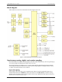
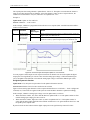
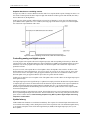
1
USB-1604HS-2AO Multifunction Synchronous Data Acquisition Board User's Guide Document Revision 3, July, 2010 © Copyright 2010, Measurement Computing Corporation Your new Measurement Computing product comes with a fantastic extra — Management committed to your satisfaction! Thank you for choosing a Measurement Computing product—and congratulations! You own the finest, and you can now enjoy the protection of the most comprehensive warranties and unmatched phone tech support. It’s the embodiment of our mission: To provide PC-based data acquisition hardware and software that will save time and save money. Simple installations minimize the time between setting up your system and actually making measurements. We offer quick and simple access to outstanding live FREE technical support to help integrate MCC products into a DAQ system. Limited Lifetime Warranty: Most MCC products are covered by a limited lifetime warranty against defects in materials or workmanship for the life of the product, to the original purchaser, unless otherwise noted. Any products found to be defective in material or workmanship will be repaired, replaced with same or similar device, or refunded at MCC’s discretion. For specific information, please refer to the terms and conditions of sale. Harsh Environment Program: Any Measurement Computing product that is damaged due to misuse, or any reason, may be eligible for replacement with the same or similar device for 50% of the current list price. I/O boards face some harsh environments, some harsher than the boards are designed to withstand. Contact MCC to determine your product’s eligibility for this program. 30 Day Money-Back Guarantee: Any Measurement Computing Corporation product may be returned within 30 days of purchase for a full refund of the price paid for the product being returned. If you are not satisfied, or chose the wrong product by mistake, you do not have to keep it. These warranties are in lieu of all other warranties, expressed or implied, including any implied warranty of merchantability or fitness for a particular application. The remedies provided herein are the buyer’s sole and exclusive remedies. Neither Measurement Computing Corporation, nor its employees shall be liable for any direct or indirect, special, incidental or consequential damage arising from the use of its products, even if Measurement Computing Corporation has been notified in advance of the possibility of such damages. HM USB-1604HS-2AO.docx 3 Trademark and Copyright Information TracerDAQ, Universal Library, Measurement Computing Corporation, and the Measurement Computing logo are either trademarks or registered trademarks of Measurement Computing Corporation. Windows, Microsoft, and Visual Studio are either trademarks or registered trademarks of Microsoft Corporation LabVIEW is a trademark of National Instruments. CompactFlash is a registered trademark of SanDisk Corporation. XBee and XBee-PRO are trademarks of MaxStream, Inc. All other trademarks are the property of their respective owners. Information furnished by Measurement Computing Corporation is believed to be accurate and reliable. However, no responsibility is assumed by Measurement Computing Corporation neither for its use; nor for any infringements of patents or other rights of third parties, which may result from its use. No license is granted by implication or otherwise under any patent or copyrights of Measurement Computing Corporation. All rights reserved. No part of this publication may be reproduced, stored in a retrieval system, or transmitted, in any form by any means, electronic, mechanical, by photocopying, recording, or otherwise without the prior written permission of Measurement Computing Corporation. Notice Measurement Computing Corporation does not authorize any Measurement Computing Corporation product for use in life support systems and/or devices without prior written consent from Measurement Computing Corporation. Life support devices/systems are devices or systems which, a) are intended for surgical implantation into the body, or b) support or sustain life and whose failure to perform can be reasonably expected to result in injury. Measurement Computing Corporation products are not designed with the components required, and are not subject to the testing required to ensure a level of reliability suitable for the treatment and diagnosis of people. 4 Table of Contents Preface About this User’s Guide .......................................................................................................................7 What you will learn from this user’s guide......................................................................................................... 7 Conventions in this user’s guide ......................................................................................................................... 7 Where to find more information ......................................................................................................................... 7 Chapter 1 Introducing the USB-1604HS-2AO ......................................................................................................8 Overview: USB-1604HS-2AO features.............................................................................................................. 8 Software features ................................................................................................................................................ 8 Chapter 2 Installing the USB-1604HS-2AO ..........................................................................................................9 What comes with your USB-1604HS-2AO shipment?....................................................................................... 9 Hardware .......................................................................................................................................................................... 9 Optional components ........................................................................................................................................................ 9 Additional documentation ................................................................................................................................................10 Signal conditioning accessories .......................................................................................................................................10 Unpacking the USB-1604HS-2AO................................................................................................................... 10 Installing the software ...................................................................................................................................... 10 Installing the hardware ..................................................................................................................................... 10 Connecting the external power supply .............................................................................................................................11 Connecting the USB-1604HS-2AO to your system .........................................................................................................11 Configuring the USB-1604HS-2AO................................................................................................................. 11 Connecting the board for I/O operations .......................................................................................................... 11 Connectors, cables, and accessory products .....................................................................................................................11 Cabling ............................................................................................................................................................. 13 Field wiring and signal termination .................................................................................................................................13 TB-102 screw terminal board connector to SCSI connector pin out ................................................................................13 Chapter 3 Functional Details ...............................................................................................................................15 Front panel ........................................................................................................................................................ 15 BNC connectors ...............................................................................................................................................................15 Status LEDs .....................................................................................................................................................................15 Rear panel ......................................................................................................................................................... 15 SCSI connector ................................................................................................................................................................15 External power connector (EXT PWR) ...........................................................................................................................16 USB connector .................................................................................................................................................................16 Analog common ...............................................................................................................................................................16 Mechanical drawing ......................................................................................................................................... 16 Block diagram .................................................................................................................................................. 17 Synchronous analog, digital, and counter sampling ......................................................................................... 17 Input clock pacing ............................................................................................................................................................17 Output clock pacing .........................................................................................................................................................18 Analog inputs.................................................................................................................................................... 18 Analog outputs.................................................................................................................................................. 18 Digital I/O......................................................................................................................................................... 18 Digital input scanning ......................................................................................................................................................18 Internal pull-up/pull-down capability (J14) .....................................................................................................................18 Digital outputs and pattern generation .............................................................................................................................19 5 USB-1604HS-2AO User's Guide Triggering ......................................................................................................................................................... 20 Hardware-based triggering ...............................................................................................................................................20 Software-based triggering ................................................................................................................................................20 Stop trigger modes ...........................................................................................................................................................21 Pre-triggering and post-triggering modes ........................................................................................................................21 Counter inputs .................................................................................................................................................. 21 Mapped channels .............................................................................................................................................................22 Counter input modes ........................................................................................................................................................22 Debounce function ...........................................................................................................................................................23 Quadrature detectors ......................................................................................................................................... 26 Overview .........................................................................................................................................................................26 Maximizing encoder accuracy .........................................................................................................................................27 Connecting the USB-1604HS-2AO to an encoder ...........................................................................................................27 Timer/pulse generators ..................................................................................................................................... 28 Using detection setpoints for output control ..................................................................................................... 29 Setpoint configuration......................................................................................................................................................30 Examples of control outputs ............................................................................................................................................31 Controlling analog and digital outputs .............................................................................................................................34 Update latency .................................................................................................................................................................34 Using the setpoint status register......................................................................................................................................35 Chapter 4 Calibrating the USB-1604HS-2AO .....................................................................................................36 Chapter 5 Specifications ......................................................................................................................................37 Analog input ..................................................................................................................................................... 37 Analog output ................................................................................................................................................... 38 Analog input calibration ................................................................................................................................... 39 Digital inputs .................................................................................................................................................... 39 Digital outputs .................................................................................................................................................. 39 Trigger sources ................................................................................................................................................. 40 Pacing sources .................................................................................................................................................. 41 Counters............................................................................................................................................................ 42 Timers ............................................................................................................................................................... 42 Quadrature decoders ......................................................................................................................................... 43 Power ................................................................................................................................................................ 43 USB specifications ........................................................................................................................................... 43 Environmental .................................................................................................................................................. 43 Mechanical ....................................................................................................................................................... 44 I/O cables, connectors and accessories ............................................................................................................. 44 Signal I/O connectors ....................................................................................................................................... 44 BNC connectors ...............................................................................................................................................................44 68-pin SCSI connector .....................................................................................................................................................45 Declaration of Conformity ..................................................................................................................46 6 Preface About this User’s Guide What you will learn from this user’s guide This user’s guide explains how to install, configure, and use the USB-1604HS-2AO so that you get the most out of its synchronous data acquisition features. This user’s guide also refers you to related documents available on our web site, and to technical support resources. Conventions in this user’s guide For more information on … Text presented in a box signifies additional information and helpful hints related to the subject matter you are reading. Caution! Shaded caution statements present information to help you avoid injuring yourself and others, damaging your hardware, or losing your data. < : > Angle brackets that enclose numbers separated by a colon signify a range of numbers, such as those assigned to registers, bit settings, etc. bold text Bold text is used for the names of objects on the screen, such as buttons, text boxes, and check boxes. For example: 1. Insert the disk or CD and click the OK button. italic text Italic text is used for the names of manuals and help topic titles, and to emphasize a word or phrase. For example: The InstaCal installation procedure is explained in the Quick Start Guide. Never touch the exposed pins or circuit connections on the board. Where to find more information For additional information relevant to the operation of your hardware, refer to the Documents subdirectory where you installed the MCC DAQ software (C:\Program Files\Measurement Computing\DAQ by default), or search for your device on our website at www.mccdaq.com. 7 Chapter 1 Introducing the USB-1604HS-2AO Overview: USB-1604HS-2AO features The USB-1604HS-2AO is a multifunction high-speed measurement and control board supported under popular Microsoft® Windows® operating systems. The device is compatible with both USB 1.1 and USB 2.0 ports, (although the speed of the module maybe limited when using USB 1.1 ports). The USB-1604HS-2AO provides the following features: Four single-ended 16-bit analog inputs, with one A/D converter per channel. The maximum sampling rate is 1.333 MS/s per channel. The input range is software programmable for ±10 V, ±2.5 V, or ±500 mV. Two synchronous 16-bit ±10 V analog outputs can generate waveforms at 1 MS/s per channel. 16 synchronous digital inputs and 16 synchronous digital outputs Four 16-bit or 32-bit counters (can be configured to be gated) Two timer/pulse generators with pulse width (duty cycle) control Three 16-bit or 32-bit quadrature detectors to measure linear and rotary position A 68-pin SCSI connector provides connections for all inputs and outputs except for the four analog inputs. Six BNC connectors provide connections for the four analog inputs, and alternate connections for the external pacer clock and external digital trigger input. The USB-1604HS-2AO samples all analog inputs, digital inputs, and counter inputs simultaneously. You can synchronize AI, AO, and DIO operations at rates of up to 1 MS/s (million samples per second), with aggregate throughput up to 8 MS/s. You can pace operations with an internal or external clock. A 500 VDC isolation barrier between the field wiring and USB interface reduces signal noise and protects the board and your computer from ground spikes. The USB 2.0 high-speed driver transfers data at rates up to 480 Mbps. The device is powered by a 10 Watt regulated external power supply that is included with shipment. Factory and self-calibration tables are stored onboard in EEPROM. Software features For information on the features of InstaCal and the other software included with your USB-1604HS-2AO, refer to the Quick Start Guide that shipped with your device. 8 Chapter 2 Installing the USB-1604HS-2AO What comes with your USB-1604HS-2AO shipment? Hardware USB-1604HS-2AO USB cable (2-meter length) External power supply and cord – 5 volts, 10 watt AC power adapter. MCC part number PS-5V2AEPS Optional components Cables Standard BNC cable CA-68-3R cable CA-68-3S (3 foot shielded cable) CA-68-6S (6 foot shielded cable) CA-68-3R (3-feet) CA-68-3S (3-feet) 9 CA-68-6S (6-feet) USB-1604HS-2AO User's Guide Installing the USB-1604HS-2AO Screw termination board with screw terminals TB-102 Additional documentation In addition to this hardware user's guide, you should also receive the Quick Start Guide (available in PDF at www.mccdaq.com/PDFmanuals/DAQ-Software-Quick-Start.pdf). This booklet supplies a brief description of the software you received with your USB-1604HS-2AO and information regarding installation of that software. Please read this booklet completely before installing any software or hardware. Signal conditioning accessories MCC provides signal termination products for use with the USB-1604HS-2AO. Refer to the "Field wiring and signal termination" section for a complete list of compatible accessory products. Unpacking the USB-1604HS-2AO As with any electronic device, take care while handling to avoid damage from static electricity. Before removing the USB-1604HS-2AO from its packaging, ground yourself using a wrist strap or by simply touching the computer chassis or other grounded object to eliminate any stored static charge. If the USB-1604HS-2AO is damaged, notify Measurement Computing Corporation immediately by phone, fax, or e-mail. Phone: 508-946-5100 and follow the instructions for reaching Tech Support. Fax: 508-946-9500 to the attention of Tech Support Email: [email protected] For international customers, contact the local distributor where you purchased the USB-1604HS-2AO. Click on this link www.measurementcomputing.com/sales.asp to locate your distributor. Installing the software Refer to the Quick Start Guide for instructions on installing the software on the Measurement Computing Data Acquisition Software CD. This booklet is available in PDF at www.mccdaq.com/PDFmanuals/DAQ-SoftwareQuick-Start.pdf. Installing the hardware Power to the USB-1604HS-2AO is provided with the 10 watt AC power adapter (PS-5V2AEPS). The power supply ships with a U.S. plug. Optional interchangeable plugs for international locations are available. 10 USB-1604HS-2AO User's Guide Installing the USB-1604HS-2AO Connecting the external power supply Connect the AC power adapter cord to the EXT. PWR connector on the device's rear panel, and plug the adapter into an electrical outlet. The POWER LED on the front panel turns on when the device is detected by the system. Connect external power before connecting the USB cable to the computer Connect the external power cable to the USB-1604HS-2AO before connecting the USB cable to the computer. This allows the USB-1604HS-2AO to inform the host computer (when the USB cable is connected) that the board requires minimal power from the computer’s USB port. Connecting the USB-1604HS-2AO to your system To connect the USB-1604HS-2AO to your system, turn the computer on, and connect a USB cable from the USB connector on the rear panel to either a USB port on the computer or external USB hub connected to the computer. When you connect the USB-1604HS-2AO for the first time, a Found New Hardware message opens as the device is detected. When the message closes, the installation is complete. Configuring the USB-1604HS-2AO All hardware configuration options on the USB-1604HS-2AO are software controlled with the exception of the digital pull-up / pull-down (described below), which is set for pull-up by default. You can select some of the configuration options using InstaCal, such as the analog input range and the trigger source. Once selected, any program that uses the Universal Library will initialize the hardware according to these selections. Connecting the board for I/O operations Connectors, cables, and accessory products The following table lists the board connectors, applicable cables, and compatible accessory products for the USB-1604HS-2AO. Board connectors, cables, and compatible hardware Parameter Specification Connector types Six standard BNC female connectors for analog input, clock input, and digital trigger input 68-pin SCSI connector Standard BNC cable CA-68-3R CA-68-3S or CA-68-6S shielded cable TB-102 screw terminal board Compatible cable for the BNC connectors Compatible cables for the 68-pin SCSI connector Compatible accessory products using the CA-68-3R, CA-68-3S, or CA-68-6S cables BNC connectors The USB-1604HS-2AO has six BNC connectors used to connect the analog input signals, external pacer clock input, and external digital trigger input. Figure 1. BNC connectors The signal names for the BNC connectors are listed below: 11 USB-1604HS-2AO User's Guide Installing the USB-1604HS-2AO BNC Label Signal connection CH0 CH1 CH2 CH3 EXT TRG EXT CLK Analog input 0 Analog input 1 Analog input 2 Analog input 3 External digital trigger input External pacer clock input EXT TRG is equivalent to the DIG TRIG signal on the SCSI connector. EXT CLK is equivalent to the XAPCR signal on the SCSI connector. Connect your signals using a standard BNC cable. 68-pin SCSI connector The signals that are available on the 68-pin SCSI connector are listed below. 68-pin SCSI connector pin out Signal name DGND (external pacer clock output) XDPCR (external pacer clock input) XAPCR DIG TRIG TMR/PWM1 TMR/PWM0 CTR3 CTR2 CTR1 CTR0 DOUT15 DOUT14 DOUT13 DOUT12 DOUT11 DOUT10 DOUT9 DOUT8 DOUT7 DOUT6 DOUT5 DOUT4 DOUT3 DOUT2 DOUT1 DOUT0 AGND DAC 1 DAC 0 AGND Reserved AGND Reserved AGND Pin Pin 68 67 66 65 64 63 62 61 60 59 58 57 56 55 54 53 52 51 50 49 48 47 46 45 44 43 42 41 40 39 38 37 36 35 34 33 32 31 30 29 28 27 26 25 24 23 22 21 20 19 18 17 16 15 14 13 12 11 10 9 8 7 6 5 4 3 2 1 Signal name DGND CTR6 Z CTR6 B CTR6 A CTR5 Z CTR5 B CTR5 A CTR4 Z CTR4 B CTR4 A DIN15 DIN14 DIN13 DIN12 DIN11 DIN10 DIN9 DIN8 DIN7 DIN6 DIN5 DIN4 DIN3 DIN2 DIN1 DIN0 AGND +5VPWR VCAL (reserved for calibration) AGND Reserved AGND Reserved AGND Connect your signals using a CA-68-3R cable, or CA-68-3S or CA-68-6S shielded cable. 12 USB-1604HS-2AO User's Guide Installing the USB-1604HS-2AO Cabling Use a CA-68-3R 68-pin ribbon expansion cable (Figure 2), or a CA-68-3S (3-foot) or CA-68-6S (6-foot) 68-pin shielded expansion cable (Figure 3) to connect signals to the USB-1604HS-2AO's 68-pin SCSI connector. Figure 2. CA-68-3R cable Figure 3. CA-68-3S and CA-68-6S shielded cable Details on these cables are available at www.mccdaq.com/usb-data-acquisition/USB-1604HS-2AO.aspx. Field wiring and signal termination You can use the following Measurement Computing screw terminal board to terminate field signals and route them into the USB-1604HS-2AO board using the CA-68-3R, CA-68-3S, or CA-68-6S cable: TB-102: Termination board with screw terminals. Details on this product are available on our web site at www.measurementcomputing.com/products/screw_terminal_bnc.aspx. A 19-inch rack mount kit (RM-TB-102) for the TB-102 termination board is also available. TB-102 screw terminal board connector to SCSI connector pin out The TB-102 terminal board is shown here. The table below lists how signals on the TB-102 are mapped to the signals on the 68-pin SCSI connector. Pin mapping between the TB-102 terminal board and the 68-pin SCSI connector 13 USB-1604HS-2AO User's Guide Installing the USB-1604HS-2AO TB1 screw terminals AGND Reserved AGND Reserved AGND VCAL +5VOUT AGND DIN0 DIN1 DIN2 DIN3 DIN4 DIN5 DIN6 DIN7 DIN8 DIN9 DIN10 DIN11 DIN12 DIN13 DIN14 DIN15 CTR4A CTR4B CTR4Z CTR5A CTR5B CTR5Z CTR6A CTR6B CTR6Z DGND DGND EGND SCSI pin 1 2 3 4 5 6 7 8 9 10 11 12 13 14 15 16 17 18 19 20 21 22 23 24 25 26 27 28 29 30 31 32 33 34 * ** TB2 screw terminals AGND Reserved AGND Reserved AGND DAC0 DAC1 AGND DOUT0 DOUT1 DOUT2 DOUT3 DOUT4 DOUT5 DOUT6 DOUT7 DOUT8 DOUT9 DOUT10 DOUT11 DOUT12 DOUT13 DOUT14 DOUT15 CTR0 CTR1 CTR2 CTR3 TMR/PWM0 TMR/PWM1 DIGTRIG XAPCR XDPCR DGND DGND EGND * Extra digital ground connectors ** EGND is connected to the SCSI connector shell. 14 SCSI pin 35 36 37 38 39 40 41 42 43 44 45 46 47 48 49 50 51 52 53 54 55 56 57 58 59 60 61 62 63 64 65 66 67 68 * ** Chapter 3 Functional Details Front panel Figure 4. USB-1604HS-2AO front panel BNC connectors The USB-1604HS-2AO has six BNC connectors that provide connections for the following signals: Four single-ended analog inputs External digital trigger input External pacer clock input These signals are also available on the 68-pin SCSI connector. Status LEDs The POWER LED lights up after the device is enumerated by the system. The ACTIVE LED lights up when the USB-1604HS-2AO is transmitting or receiving data. Rear panel Figure 5. USB-1604HS-2AO rear panel SCSI connector The 68-pin SCSI connector provides connections for all I/O signals except for analog input: Refer to page 12 for the connector pin out. Two analog outputs (DAC0 and DAC1) 16 digital inputs (DIN1 to DIN15) 16 digital outputs (DOUT1 to DOUT15) Four counters (CTR0 to CTR3). Two counters may be gated. Three quadrature detectors (CTR4 A, B, and Z to CTR6 A, B, and Z) Two timer/pulse outputs (TMR/PWM0 to TMR/PWM1) Digital trigger input (DIG TRIG) Input pacer clock (XAPCR) Output pacer clock (XDPCR) Analog ground (AGND) Digital ground (DGND) Calibration (VCAL) +5V PWR 15 USB-1604HS-2AO User's Guide Functional Details External power connector (EXT PWR) The USB-1604HS-2AO requires external power. Connect the PS-5V2AEPS power supply to the EXT PWR connector. This power supply provides 5 VDC, 2 A power, and plugs into a standard 120 VAC outlet. USB connector The USB connector provides communication with the host PC. Analog common The analog ground reference for the analog inputs and analog outputs. Mechanical drawing Figure 6. USB-1604HS-2AO case dimensions 16 USB-1604HS-2AO User's Guide Functional Details Block diagram USB-1604HS-2AO functions are illustrated in the block diagram shown here. Figure 7. USB-1604HS-2AO functional block diagram Synchronous analog, digital, and counter sampling The USB-1604HS-2AO samples all analog, digital, and counter inputs simultaneously, while also generating up to two analog outputs and digital pattern outputs at the same time. The maximum analog input sampling rate is 1.33 MS/s. Digital channels (digital input and counter channels) can be sampled at rates up to 8 MS/s for one channel when no analog channels are sampled, and rates of up to 1.33 MS/s when analog channels are also sampled. Input clock pacing Analog, digital, and counter inputs can be sampled based on either an internal programmable input pacer or with an external clock source (XAPCR pin on the SCSI connector or the EXT CLK BNC connector). Analog channels can be paced from 0.75 µs to 1000 seconds in 20.83 ns steps. Digital and counter inputs can be paced from 250 ns to 1 second in 20.83 ns steps. 17 USB-1604HS-2AO User's Guide Functional Details The clock rate is 8 MHz maximum for both the internal pacer clock and external input scan clock. Output clock pacing Analog, digital, and timer operations can be paced using the internal output pacer clock (independent of the internal pacer clock), an external output pacer clock connected to the XDPCR pin on the SCSI connector, the internal programmable input pacer, or an external input pacing clock connected to either the XAPCR pin on the SCSI connector or the EXT CLK BNC connector. The clock rate is 1 MHz maximum for analog output operations, and 8 MHz maximum for digital operations in which no analog channels are enabled. Analog inputs The USB-1604HS-2AO has four single-ended analog inputs. Each input has a dedicated 16 bit A/D converter that provides true simultaneous sampling at rates of up to 1.33 MHz per channel. The input range is software selectable for ±10 V, ±2.5 V, or ±500 mV. You can pace analog input operations with the internal A/D pacer clock or with an external clock source. When using an external input scan clock, connect the clock source to the XAPCR pin on the SCSI connector or the EXT CLK BNC connector. Analog outputs The USB-1604HS-2AO has two independent, 16-bit, analog output channels. The analog output range is -10V to +10V. Each DAC channel can continuously output a waveform at up to 1 MHz. You can clock the DAC channels with the internal DAC scan clock or with an external DAC input clock. The internal analog input pacer clock can pace both the DAC output and the analog input simultaneously. When using an external output scan clock, connect the clock source to the XDPCR pin on the SCSI connector or the EXT CLK BNC connector. Digital I/O The USB-1604HS-2AO has 32 CMOS digital I/O lines configured as 16 digital inputs and 16 digital outputs. You can pace digital operations with the onboard scan clock or an external source. The maximum DIO transfer rate is 8 MS/s (software paced). Digital input scanning Digital input ports can be read synchronously along with analog channels in a scan, or asynchronously before, during, or after an analog input scan. The digital inputs can sustain rates of up to 8 MS/s for one channel when no analog channels are sampled, and rates of up to 1.33 MS/s when analog channels are also sampled. Internal pull-up/pull-down capability (J14) Unconnected inputs are pulled high to +3.3V through 100 k resistors via a 4-pin jumper on the PCB board (J14). To configure these inputs to pull low (0 V), do the following: 1. Remove the 4 screws from the rear panel. 18 USB-1604HS-2AO User's Guide Functional Details Figure 8. Location of rear panel screws 2. Slide the board out of the housing and locate jumper J14. Figure 9. Location of J14 3. Configure jumper J14 for either pull-up or pull-down configuration (refer to Figure 10). o o For pull-up, place the J14 shorting block across pins 1 and 2. For pull-down, place the J14 shorting block across pins 3 and 4. Figure 10. J14 configuration 4. Slide the board into the housing. 5. Replace the 4 screws on the rear panel. Digital outputs and pattern generation Digital outputs can be updated asynchronously at any time before, during, or after an acquisition. The USB1604HS-2AO can generate a digital pattern at up to 4 MS/s. Digital pattern generation is clocked with either the internal D/A scan clock or with an external D/A input clock. Digital patterns can be generated along with D/A waveforms. They are paced by the same selected clock. The on-board programmable clock generates updates ranging from once every 1000 seconds to 1 MHz, independent of the acquisition rate. The digital outputs are driven low at power up and reset. 19 USB-1604HS-2AO User's Guide Functional Details Triggering Triggering can be the most critical aspect of a data acquisition application. A trigger event occurs and data acquisition begins when specified conditions are met. You select the trigger mode and set up its parameters with software. The USB-1604HS-2AO supports both hardware-based and software-based triggers. With a hardware-based trigger, an output value is compared in hardware to an input level on a specified channel. With software-based triggers, the analog, digital, and/or counter readings are checked by the PC in order to detect the trigger event. The USB-1604HS-2AO supports the following trigger sources: Hardware-based triggers: o Analog input hardware o External digital trigger input Software-based triggers: o Analog software trigger o Digital pattern o Counter/totalizer Hardware-based triggering With a hardware-based trigger, an output value is compared in hardware to an input level on a specified channel. Analog input hardware In this mode, the acquisition is triggered when a specified input level is achieved. The USB-1604HS-2AO uses true analog triggering in which the trigger level you program sets an analog DAC, which is then compared in hardware to the analog input level on the selected channel. This ensures an analog trigger latency that is less than 1.5 µs. You can select any analog channel as the trigger channel, but the selected channel must be the first channel in the scan. You can program the trigger level, the rising or falling edge, and hysteresis level. The trigger level can be any value within the voltage range for the selected trigger channel. External digital trigger input A separate digital trigger input line (DIG TRIG) allows TTL-level triggering with latencies guaranteed to be no less than 100 nS. The acquisition is triggered when a rising or falling edge is detected . The trigger level is set at TTL sensitive. Latency is one sample period, maximum. The input signal range is ±15 V. The trigger edge, logic level (1 or 0), and the rising or falling edge for the discrete trigger input are software selectable. Software-based triggering The three software-based trigger modes differ from hardware analog triggering and digital triggering because the analog, digital, or counter readings are checked by the PC in order to detect the trigger event. Analog software The acquisition is triggered when the computer issues a software command. You can select any analog channel in the scan as the trigger channel. The trigger level, the rising or falling edge, and hysteresis are software programmable. The trigger level can be any value within the range of the trigger channel. Latency is one sample period, maximum. Digital pattern The acquisition is triggered with a digital input channel pattern. You can select any scanned digital input channel pattern to trigger an acquisition, including the ability to mask or ignore specific bits. You can program to trigger the conversion when equal to, not equal to, above, or below a value. Latency is one sample period, maximum. 20 USB-1604HS-2AO User's Guide Functional Details Counter/Totalizer The acquisition is triggered with the counter/totalize inputs. You can program triggering to occur on a frequency, or on total counts that are equal, not equal, above, below, or below a value, or that are within/outside of a window rising/falling edge. Latency is one sample period, maximum. You can select of the included counter channels as the trigger source. Software-based triggering usually results in a long period of inactivity between the trigger condition being detected and the data being acquired. However, the USB-1604HS-2AO avoids this situation by using pre-trigger data. When software-based-triggering is used, and the PC detects the trigger condition — which may be thousands of readings after the actual occurrence of the signal — the USB-1604HS-2AO driver automatically looks back to the location in memory where the actual trigger-causing measurement occurred, and presents the acquired data that begins at the point where the trigger-causing measurement occurs. The maximum inactive period in this mode equals one scan period. Set the trigger value > 0 when using a counter input as the trigger source When using a counter for a trigger source, set the trigger value to 1 or greater. Since all counters start at zero with the first scan, there is no valid reference in regard to rising or falling edge. Setting the trigger value to 1 or greater ensures that a valid reference value is present, and that the first trigger will be legitimate. Stop trigger modes You can use any of the software trigger modes explained previously to stop an acquisition. For example, you can program an acquisition to begin on one event, such as a voltage level, and then stop on another event, such as a digital pattern. Pre-triggering and post-triggering modes The USB-1604HS-2AO supports four modes of pre-triggering and post-triggering. When using pre-trigger, you must use software-based triggering to initiate an acquisition. No pre-trigger, post-trigger stop event In this mode, data acquisition starts when the trigger is received, and the acquisition stops when the stop-trigger event is received. Fixed pre-trigger with post-trigger stop event In this mode, you set the number of pre-trigger readings to acquire. The acquisition continues until a stoptrigger event occurs. No pre-trigger, infinite post-trigger In this mode, no pre-trigger data is acquired. Instead, data is acquired beginning with the trigger event, and is terminated when you issue a command to halt the acquisition. Fixed pre-trigger with infinite post-trigger You set the amount of pre-trigger data to acquire. Then, the system continues to acquire data until the program issues a command to halt acquisition. Counter inputs The USB-1604HS-2AO has four counters that can accept frequency inputs up to 20 MHz. The counter channels can be read as 16 or 32-bit counters. A counter can also be configured to be gated by one of the other counter inputs mapped as a gate input (refer to Mapped channels, on page 22). The input type is TTL, rising-edge triggered. The counters can concurrently monitor time periods, frequencies, pulses, and other event driven incremental occurrences directly from pulse-generators, limit switches, proximity switches, and magnetic pick-ups. Counter inputs can be read asynchronously under program control, or synchronously as part of an analog or digital scan group. 21 USB-1604HS-2AO User's Guide Functional Details When reading synchronously, all counters are set to zero at the start of an acquisition. When reading asynchronously, counters may be cleared on each read, count up continually, or count until the 16-bit or 32-bit limit has been reached. See the counter mode descriptions below. Figure 11. Typical USB-1604HS-2AO counter channel Mapped channels A mapped channel is one of four counter input signals (CTR0 to CTR3) that can get multiplexed into a counter module. The mapped channel can participate with the counter's input signal by gating the counter, latching the counter, and so on. The four possible choices for the mapped channel are the four counter input signals (postdebounce). A mapped channel can be used to: gate the counter decrement the counter latch the current count to the count register Usually, all counter outputs are latched at the beginning of each scan within the acquisition. However, you can use a second channel — known as the mapped channel — to latch the counter output. Counter input modes The USB-1604HS-2AO supports the following modes: Counter Period Pulse width measurement Timing Program the counter operation mode with software. Counter mode A counter can be asynchronously read with or without clear on read. The asynchronous read-signals strobe when the lower 16-bits of the counter are read by software. The software can read the counter's high 16-bits some time later after reading the lower 16-bits. The full 32-bit result reflects the timing of the first asynchronous read strobe. The following counter mode options are selectable with software. 22 USB-1604HS-2AO User's Guide Functional Details Counter mode Description Totalize This mode allows the basic use of a 32-bit counter. The channel input increments the counter upward. When used as a 16-bit counter (counter low), one channel can be scanned up to an 8 MHz rate. When used as a 32-bit counter (counter high), two sample times are used to return the full 32-bit result. Therefore, a 32-bit counter can only be sampled at a 4 MHz maximum rate. The counter counts up and does not clear on every new sample. However, it does clear at the start of a new scan command. The counter rolls over on the 16-bit (counter low) boundary, or on the 32-bit (counter high) boundary. The counter counts up and is cleared after each read. By default, the counter counts up and only clears the counter at the start of a new scan command. The value of the counter before it was cleared is latched and returned. The counter continues to count upward, rolling over on the 16 or 32-bit boundary. The counter stops at the top of its count. The top of the count is FFFF hex (65,535) for the 16-bit mode, and FFFFFFFF hex (4,294,967,295) for the 32-bit mode. Sets the counter type to either 16-bits or 32-bits. The type of counter only matters if the counter is using the Stop at all FFFFs mode; otherwise, this option is ignored. The 16 bit mode requires less bandwidth for higher channels count and higher sample rates. Clear on read Rollover Stop at top 16-bit or 32-bit Period mode This mode allows for period measurement of the channel input. You can measure x1, x10, x100 or x1000 periods, and 16-bit (counter low) or 32-bit (counter high) values. Four timebase, or tick-size, values are available (20.83 ns, 208.3 ns, 2.083 µs, or 20.83 µs). These values are based on the 48 MHz system clock. Any other channel can gate the period measurement. All period mode options are selectable with software. Pulse width measurement mode This mode is used to measure a channel's pulse width. You can measure 16-bit or 32-bit values. Four timebase, or tick-size, values are available (20.83 ns, 208.3 ns, 2.083 µs, or 20.83 µs). These values are based on the 48 MHz system clock. Any other channel can gate the pulse width measurement. All pulse width options are selectable with software. Timing mode This mode is used to measure the time between two subsequent events, such as the edge of one channel with respect to the edge of another channel. You can measure 16-bit or 32-bit values. Four timebase, or tick-size, values are available (20.83 ns, 208.3 ns, 2.083 µs, or 20.83 µs) . All timing options are selectable with software. Debounce function The USB-1604HS-2AO has debounce circuitry which eliminates switch-induced transients that are typically associated with electro-mechanical devices including relays, proximity switches, and encoders. All debounce options are selectable with software. You can select a debounce time, debounce mode, and risingedge or falling-edge sensitivity. Each channel's output can be debounced with 16 programmable debounce times in the range of 500 ns to 25.5 ms). There are two debounce modes, as well as a debounce bypass, as shown in Figure 12. The signal from the buffer can be inverted before it enters the debounce circuitry. The inverter is used to make the input rising-edge or falling-edge sensitive. Edge selection is available with or without debounce. In this case the debounce time setting is ignored and the input signal goes straight from the inverter or inverter bypass to the counter module. The two debounce modes are trigger after stable and trigger before stable. In either mode, the selected debounce time determines how fast the signal can change and still be recognized. 23 USB-1604HS-2AO User's Guide Functional Details Figure 12. Debounce model block diagram Trigger after stable mode In the trigger after stable mode, the output of the debounce module does not change state until a period of stability has been achieved. This means that the input has an edge, and then must be stable for a period of time equal to the debounce time. Figure 13. Debounce module – trigger after stable mode T1 through T5 indicate time periods. In trigger after stable mode, the input signal to the debounce module is required to have a period of stability after an incoming edge, in order for that edge to be accepted (passed through to the counter module.) For this example, the debounce time is equal to T2 and T5. T1 – In Figure 13, the input signal goes high at the beginning of time period T1, but never stays high for a period of time equal to the debounce time setting (equal to T2 for this example.) T2 – At the end of time period T2, the input signal has transitioned high and stayed there for the required amount of time—therefore the output transitions high. If the input signal does not stabilize in the high state long enough, no transition would have appeared on the output and the entire disturbance on the input would have been rejected. T3 – During time period T3, the input signal remained steady. No change in output is seen. T4 – During time period T4, the input signal has more disturbances and does not stabilize in any state long enough. No change in the output is seen. T5 – At the end of time period T5, the input signal has transitioned low and stayed there for the required amount of time—therefore the output goes low. Trigger before stable mode In the trigger before stable mode, the output of the debounce module immediately changes state, but will not change state again until a period of stability has passed. For this reason the mode can be used to detect glitches. Figure 14. Debounce module – Trigger before stable mode T1 through T5 indicate time periods. T1 – In Figure 14, the input signal is low for the debounce time (equal to T1); therefore when the input edge arrives at the end of time period T1, it is accepted and the output (of the debounce module) goes high. Note that a period of stability must precede the edge in order for the edge to be accepted. 24 USB-1604HS-2AO User's Guide Functional Details T2 – During time period T2, the input signal is not stable for a length of time equal to T1 (the debounce time setting for this example.) Therefore, the output stays "high" and does not change state during time period T2. T3 – During time period T3, the input signal is stable for a time period equal to T1, meeting the debounce requirement. The output is held at the high state. This is the same state as the input. T4 – At anytime during time period T4, the input can change state. When this happens, the output will also change state. At the end of time period T4, the input changes state, going low, and the output follows this action [by going low]. T5 – During time period T5, the input signal again has disturbances that cause the input to not meet the debounce time requirement. The output does not change state. T6 – After time period T6, the input signal has been stable for the debounce time and therefore any edge on the input after time period T6 is immediately reflected in the output of the debounce module. Debounce mode comparisons Figure 15 shows how the two modes interpret the same input signal, which exhibits glitches. Notice that the trigger before stable mode recognizes more glitches than the trigger after stable mode. Use the bypass option to achieve maximum glitch recognition. Figure 15. Example of two debounce modes interpreting the same signal Set the debounce time according to the amount of instability expected in the input signal. Setting a debounce time that is too short may result in unwanted glitches clocking the counter. Setting a debounce time that is too long may result in an input signal being rejected entirely. Some experimentation may be required to find the appropriate debounce time for a particular application. To see the effects of different debounce time settings, view the analog waveform along with the counter output. This can be done by connecting the source to an analog input. Use trigger before stable mode when the input signal has groups of glitches and each group is to be counted as one. The trigger before stable mode recognizes and counts the first glitch within a group but rejects the subsequent glitches within the group if the debounce time is set accordingly. The debounce time should be set to encompass one entire group of glitches as shown in the following diagram. Figure 16. Optimal debounce time for trigger before stable mode 25 USB-1604HS-2AO User's Guide Functional Details Trigger after stable mode behaves more like a traditional debounce function: rejecting glitches and only passing state transitions after a required period of stability. Trigger after stable mode is used with electro-mechanical devices like encoders and mechanical switches to reject switch bounce and disturbances due to a vibrating encoder that is not otherwise moving. The debounce time should be set short enough to accept the desired input pulse but longer than the period of the undesired disturbance as shown in Figure 17. Figure 17. Optimal debounce time for trigger after stable mode Quadrature detectors Overview Quadrature detectors are used to calculate the relative or absolute position of a quadrature encoder, and to determine its rotational speed. Each quadrature detector supports phase A, B, and Z input signals (0 , 90 , and zero). When reading phase A, phase B, and index Z signals, the positioning, direction, and velocity data can be calculated. Quadrature encoders generally have three outputs: A, B, and Z. The A and B signals are pulse trains driven by an optical sensor inside the encoder. As the encoder shaft rotates, a laminated optical shield rotates inside the encoder. The shield has three concentric circular patterns of alternating opaque and transparent windows through which an LED shines. There is one LED and one phototransistor for each of the concentric circular patterns. One phototransistor produces the A signal, another phototransistor produces the B signal and the last phototransistor produces the Z signal. The concentric pattern for A has 512 window pairs (or 1024, 4096, etc.) When using a counter for a trigger source, use a trigger value of at least 1. Since all counters start at zero with the initial scan, there is no valid reference in regard to rising or falling edge. Setting a pre-trigger to 1 or more ensures that a valid reference value is present, and that the first trigger is legitimate. Figure 18. Concentric pattern for output A The concentric pattern for B has the same number of window pairs as A, except that the entire pattern is rotated by ¼ of a window-pair. Thus the B signal is always 90º out of phase from the A signal. The A and B signals pulse 512 times (or 1024, 4096, etc.) per complete rotation of the encoder. The concentric pattern for the Z signal has only one transparent window and therefore pulses only once per complete rotation. Representative signals are shown in Figure 19. 26 USB-1604HS-2AO User's Guide Functional Details A B Z Figure 19. Representation of quadrature encoder outputs A, B, and Z As the encoder rotates, the A (or B) signal indicates the distance the encoder has traveled. The frequency of A (or B) indicates the velocity of rotation of the encoder. If the Z signal is used to zero a counter (that is clocked by A) then that counter gives the number of pulses the encoder has rotated from its reference. The Z signal is a reference marker for the encoder. It should be noted that when the encoder is rotating clockwise (as viewed from the back), A will lead B and when the encoder is rotating counterclockwise, A lags behind B. If the counter direction control logic is such that the counter counts upward when A leads B and counts downward when A lags B, then the counter gives direction control as well as distance from the reference. Maximizing encoder accuracy If there are 512 pulses on A, then the encoder position is accurate to within 360°/512. You can get even greater accuracy by counting not only rising edges on A but also falling edges on A, giving position accuracy to 360°/1024. You get maximum accuracy counting rising and falling edges on A and on B (since B also has 512 pulses.) This gives a position accuracy of 360°/2048. These different modes are known as X1, X2, and X4. Connecting the USB-1604HS-2AO to an encoder You can connect up to three encoders to the USB-1604HS-2AO. Quadrature encoders with a 16-bit (counter low) or a 32-bit (counter low + counter high) counter, 6 MHz maximum pulse frequency, and X1, X2, and X4 count modes are supported. The SCSI connector provides six counter pins that are dedicated to performing encoder functions: CTR4 A, CTR4 B, CTR4 Z CTR5 A, CTR5 B, CTR5 Z CTR6 A, CTR6 B, CTR6 Z The encoder input pins are dedicated for encoder counting, and cannot be mapped for other functions. Input A is a direct counter input. Input B functions as the B phase for encoder counting, and Input Z functions as the Z phase of the encoder. Each A and B signal is made as a single-ended connection with respect to common ground. To connect an encoder to the USB-1604HS-2AO, do the following: Connect signals A, B, and Z to the CTR4 A, B, and Z through CTR6 A, B, and Z pins on the SCSI connector. Connect each encoder ground to GND. Figure 20 shows the connections for one encoder to the 68-pin SCSI connector on a USB-1604HS-2AO. 27 USB-1604HS-2AO User's Guide Functional Details +5V PWR Ground (to DGND pin) CTR4 A to Encoder “A” CTR4 B to Encoder “B” CTR4 Z to Encoder “Z” Encoder Figure 20. Encoder connections to the SCSI connector* * Connections can alternately be made to the associated screw-terminals of a connected TB-102 terminal connector. You can get the relative position and velocity from the encoder. However, during an acquisition, you cannot get data that is relative to the Z-position until the encoder locates the Z-reference. Debounce feature Each input can be debounced from 500 ns to 25.5 ms (total of 16 selections) to eliminate extraneous noise, or to switch induced transients. Encoder input signals must be within 0 and 5.5 volts and the switching threshold is typically 1.5 volts. If the encoder stops rotating, but continues to generate signals (due to it being mounted to a vibrating or noisy machine), you can use the debounce feature to eliminate false edges. Choose an appropriate debounce time and apply it to each encoder channel. Refer to the "Debounce function" section on page 23 for additional information regarding debounce times. Scan period values The USB-1604HS-2AO clears all counter channels at the beginning of the acquisition, so the values returned during scan period 1 are always zero. The values returned during scan period 2 reflect what happened during scan period 1. In general, the output of each channel’s counter is latched at the beginning of each scan period (called the start-of-scan.) Every time the USB-1604HS-2AO receives a start-of-scan signal, the counter values are latched and are available to the USB-1604HS-2AO. The scan period defines the timing resolution for the USB-1604HS-2AO. If you need a higher timing resolution, shorten the scan period. Timer/pulse generators The USB-1604HS-2AO has two timer/pulse generator signals (TMR/PWM0 and TMR/PWM1) with programmable duty cycle. Each timer is capable of generating a programmable pulse width wave with a programmable frequency in the range of 0.01123 Hz to 24 MHz. The pulse and period range is 20.83 ns to 89 seconds. Figure 21. Typical timer/pulse generator channel 28 USB-1604HS-2AO User's Guide Functional Details The timer outputs can be updated asynchronously at any time, however, doing so results in a pulse stream that is not seamless. Using detection setpoints for output control You can configure a detection setpoint for each analog input channel. Each setpoint can update the following channels, allowing for real-time control based on acquisition data: The upper 8-bits of the digital output port with a data byte and mask byte analog outputs (DAC 0, DAC 1) You can configure each detection setpoint as one of the following: Single point referenced – Above, below, or equal to the defined setpoint. Window (dual point) referenced – Inside or outside the window. Window (dual point) referenced, hysteresis mode – Outside the window high forces one output (designated as Output 2); outside the window low forces another output (designated as Output 1). Figure 22. Setpoint configuration A digital detect signal is used to indicate when a signal condition is True or False. A signal condition is true if the signal has met defined criteria, and false if the signal has not met defined criteria. The detect signals can be measured as any other input channel, thus allowing real time data analysis during an acquisition. The detection module looks at the 16-bit data being returned on a channel and generates another signal for each channel with a setpoint applied (Detect1 for Channel 1, Detect2 for Channel 2, and so on; see Figure 23). These signals serve as data markers for each channel's data. It does not matter whether that data is volts or counts. A channel's detect signal shows a rising edge and is True (1) when the channel's data meets the setpoint criteria. The detect signal shows a falling edge and is False (0) when the channel's data does not meet the setpoint criteria. The True and False states for each setpoint criteria appear in the setpoint status register; refer to "Using the setpoint status register" section on page 35 for more information. Criteria – input signal is equal to X Action - driven by condition Compare X to: Setpoint definition Update conditions Limit A or Limit B Equal to A (X = A) Below A (X < A) Above B (X > B) (choose one) Window* (non-hysteresis mode) Inside (B < X < A) Outside: B > X; or X > A (choose one) True only: If True, then output value 1 If False, then perform no action True and False: If True, then output value 1 If False, then output value 2 True only: If True, then output value 1 If False, then perform no action True and False: If True, then output value 1 If False, then output value 2 29 USB-1604HS-2AO User's Guide Functional Details Criteria – input signal is equal to X Window* (hysteresis mode) Above A (X > A) Below B (X < B) (both conditions are checked in hysteresis mode) Action - driven by condition Hysteresis mode (forced update): If X > A is True, then output value 2 until X < B is True, then output value 1. If X < B is True, then output value 1 until X > A is True, then output value 2. This is saying: (a) If the input signal is outside the window high, then output value 2 until the signal goes outside the window low, and (b) if the signal is outside the window low, then output value 1 until the signal goes outside the window high. There is no change to the detect signal while within the window. * Value A defines the upper limit of the Window, and Value B defines the lower limit. The detect signal has the timing resolution of the scan period, as shown in Figure 23. The detect signal can change no faster than the scan frequency (1/sampling period.) Detect1 Detect2 Detect3 Acquisition stream Scan Group Sampling Period 1 s Figure 23. Detection signals for channels 1, 2, and 3 Each channel in the scan group can have one detection setpoint. There can be no more than 16 total setpoints total applied to channels within a sampling group. Detection setpoints act on 16-bit data only. When reading the counters as 32-bit, data is returned 16-bits at a time. The lower word, the higher word, or both lower and higher words can be part of the scan group. Each counter input channel can have one detection setpoint for the counter's lower 16-bit value, and one detection setpoint for the counter's higher 16-bit value. Setpoint configuration You program all setpoints as part of the pre-acquisition setup, similar to setting up an external trigger. Each setpoint acts on 16-bit data, so each has two 16-bit compare values: a high limit (limit A) and a low limit (limit B). These limits define the setpoint window. You can set the 16-bit high limit (limit A) and the 16-bit low limit (limit B) with software. The setpoint conditions (criteria) and update modes are summarized below. Setpoint criteria Inside window Outside window The signal is below the 16-bit high limit (limit A) and above the 16-bit low limit (limit B). The signal is above the 16-bit high limit (limit A), or below the 16-bit low limit (limit B). 30 USB-1604HS-2AO User's Guide Greater than value Less than value Equal to value Functional Details The signal is above the 16-bit low limit. The 16-bit high limit (limit A) is not used. The signal is below the 16-bit high limit. The 16-bit low limit (limit B) is not used. The signal is equal to the 16-bit high limit. The 16-bit low limit (limit B) is not used. This mode is intended for use when the counter or digital input channels are the source channel. Only use this mode with counter or digital input channels as the channel source. To have similar functionality for analog channels, use the inside window mode. Outside the window high forces output 2 until an outside the window low condition exists, then output 1 is forced. Output 1 continues until an outside the window high condition exists. This cycle repeats as long as the acquisition is running in hysteresis mode. Hysteresis mode Setpoint output channel None Update the upper 8-bits of the digital output port Update the analog output channels (DAC0, DAC1) Update modes Update on True only Update on True and False None – Do not update Setpoint values for output 16-bit DAC value or the most significant byte (MSB) of the digital output port when the input does meets criteria. 16-bit DAC value or the most significant byte (MSB) of the digital output port when the input does not meet criteria. Note: When using setpoints with triggers other than immediate, hardware analog, or TLL, the setpoint criteria evaluation begins immediately upon triggering the acquisition. Examples of control outputs Detection on analog input, DAC, and digital port MSB updates Example 1: Update mode: Update on True and False Criteria: Channel 1 — below limit In this example, channel 1 is programmed with reference to one setpoint (limit A), defining a low limit. Channel Condition State of detect signal Action 1 Below limit A (for channel 1) True When the channel 1 analog input voltage is below limit A, update DAC1 with the output value 0.0 V. When the above condition is false, update DAC1 with the output value of minus 1.0 V. False Figure 24. Channel 1 input with setpoint update on True and False 31 USB-1604HS-2AO User's Guide Functional Details The setpoint placed on analog Channel 1 updated DAC1 with 0.0 V. The update occurred when the channel 1 input was less than setpoint limit A. When the value of the channel 1 input was above setpoint limit A, the condition of less than limit A was false, and DAC1 was updated with –1.0 V. Example 2: Update mode: Update on True and False Criteria: Channel 0 — inside window In this example, Channel 0 is programmed with reference to two setpoints (limit A and limit B) which define a window for that channel. Channel Condition State of detect signal Action 0 Within window (between limit A and limit B) for channel 0 True When Channel 0 analog input voltage is within the window, update the digital output port's MSB with 70h. When the above condition is false (channel 0 analog input voltage is outside the window), update the digital output port's MSB with 30h. False Figure 25. Channel 0 input with setpoint update on True and False You can program control outputs on each setpoint. Detection for channel 0 can be used to update the digital output port's most significant byte with one value when the analog input voltage is within the shaded region (70 h), and update with a different value when the analog input voltage is outside the shaded region (30 h). Using the hysteresis function Update mode: N/A, the hysteresis option has a forced update built into the function Criteria used: Window criteria for above and below the set limits Figure 26 shows analog input Channel 3 with a setpoint which defines two 16-bit limits — Limit A (High) and Limit B (Low). These limits are applied in the hysteresis mode and DAC channel 0 is updated accordingly. In this example, Channel 3's analog input voltage is used to update DAC0, as follows: When outside the window, low (below limit B) DAC0 is updated with 3.0 V. This update remains in effect until the analog input voltage goes above Limit A. When outside the window, high (above limit A), DAC0 is updated with 7.0 V. This update remains in effect until the analog input signal falls below limit B. At that time we are again outside the limit "low" and the update process repeats itself. Hysteresis mode can also be done with the digital output port's most significant byte instead of a DAC. 32 USB-1604HS-2AO User's Guide Functional Details Figure 26. Channel 3 in hysteresis mode Using multiple inputs to control one DAC output Update mode: Rising edge, for each of two channels Criteria used: Inside window, for each of two channels Figure 27 shows how multiple inputs can update one output. In this figure, analog output channel DAC1 is being updated. Analog input Channel 1 has an inside-the-window setpoint applied. Whenever Channel 1's input goes inside the programmed window, DAC1 will be updated with 3.0 V. Analog input Channel 2 also has an inside-the-window setpoint applied. Whenever channel 2's input goes inside the programmed window, DAC1 is updated with –7.0 V. Figure 27. Using two criteria to control an output The update on True only mode was selected, and therefore the updates for DAC1 only occur when the criteria is met. However, in the above figure we see that there are two setpoints acting on one DAC. We can also see that the two criteria can be met simultaneously. When both criteria are True at the same time, the DAC1 voltage is associated with the criteria that has been most recently met. 33 USB-1604HS-2AO User's Guide Functional Details Setpoint detection on a totalizing counter In Figure 28, CTR1 is a counter channel in totalize mode. Two setpoints define a point of change for Detect 1 as the counter counts upward. The detect output is high when inside the window (greater than limit B (low limit)) but less than limit A (the high limit). In this case, the CTR1 setpoint is defined for the 16 lower bits of channel 1's 32-bit value. The digital output port's MSB could be updated on a True condition (the rising edge of the detection signal). You can also update one of the DAC output channels with a value. Figure 28. CTR1 in totalizing counter mode, inside the window setpoint Controlling analog and digital outputs You can program each setpoint with an 8-bit digital output byte and corresponding 8-bit mask byte. When the setpoint criteria is met, the digital output port's most significant byte (MSB) can be updated with the given byte and mask. You can also program each setpoint with a 16-bit DAC update value. Either DAC output can be updated in real time. In hysteresis mode, each setpoint has two forced update values. Each update value can drive one DAC or the digital output port's most significant byte. In hysteresis mode, the outputs do not change when the input values are inside the window. One update value gets applied when the input values are less than the window, and a different update value gets applied when the input values are greater than the window. Update on True and False uses two update values. The update values can drive DACs or the digital output port's most significant byte. The digital output port's most significant byte is updated one sample period after the detection setpoint channel is sampled, plus up to 250 ns for data transfer from the detection setpoint channels. DAC output is updated one sample period after the detection setpoint channel is sampled, plus up to 1 µs for data transfer from the detection setpoint channels and data shifting out to the D/A converter. Update latencies can be improved with an increased sample rate. When using setpoints to control the DAC outputs, increased latencies may occur if attempting to stream data to DACs or pattern digital output at the same time. The increased latency can be as long as the period of the DAC pacer clock. For these reasons, avoid streaming outputs on any DAC or pattern digital output when using setpoints to control DACs. Update latency USB-1604HS-2AO channels are read almost immediately. The response for a channel input detection does not occur until the next reading is taken, during the next tick of the acquisition clock. The maximum update latency is one sample period plus 250 ns for the most significant byte (MSB) of the digital output port, and 1 µs for DAC updates. 34 USB-1604HS-2AO User's Guide Functional Details The detection circuit works on data that is put into the acquisition stream at the sample rate. This data is acquired according to the pre-acquisition setup (sampling group, sample period, etc.) and returned to the PC. Counters are latched into the acquisition stream when sampling begins. The actual counters may be counting much faster than the sample rate, and therefore only every 10th, 100th, or nth count shows up in the acquisition data. As a result, you can set a small detection window on a totalizing counter channel and have the detection setpoint "stepped over" since the sample period was too long. Even though the counter value stepped into and out of the detection window, the actual values going back to the PC may not. This is true no matter what mode the counter channel is in. When setting a detection window, keep a sample period in mind. This applies to analog inputs and counter inputs. Quickly changing analog input voltages can step over a setpoint window if not sampled often enough, resulting in missed setpoint event. There are three possible solutions for overcoming this problem: Shorten the sample period to give more timing resolution on the counter values or analog values. Widen the setpoint window by increasing limit A and/or lowering limit B. A combination of both of the above solutions could be made. Using the setpoint status register You can use the setpoint status register to check the current state of the 16 possible setpoints. In the register, Setpoint 0 is the least significant bit, and setpoint 15 is the most significant bit. Each setpoint is assigned a value of 0 or 1. A value of 0 indicates that the setpoint criteria is not met — the condition is False. A value of 1 indicates that the criteria is met — the condition is True. In the following example, the criteria for setpoints 0, 1, and 4 is satisfied (True), but the criteria for the other 13 setpoints is not met. Setpoint # True (1) False (0) 15 0 14 0 13 0 12 0 11 0 10 0 9 0 8 0 7 0 6 0 5 0 4 1 <<< Most significant bit 2 0 1 1 0 1 Least significant bit >>> From the above table we have 10011 binary, or 19 decimal; it is derived as follows: 3 0 Setpoint 0, having a True state, shows 1, giving us decimal 1. Setpoint 1, having a True state, shows 1, giving us decimal 2. Setpoint 4, having a True state, shows 1, giving us decimal 16. For proper operation, the setpoint status register must be the last channel sampled. 35 Chapter 4 Calibrating the USB-1604HS-2AO Every range of a USB-1604HS-2AO device is calibrated at the factory using a NIST traceable calibration process. Correction factors for each range are stored on the unit at the time of calibration. The analog input calibration can be adjusted in the field without destroying the factory calibration. This is accomplished by having two independent calibration tables in the on-board EPROM: one table contains the original factory calibration, and the other table is used to store field calibration constants. You can perform field calibration automatically in seconds with InstaCal and without the use of external hardware or instruments. Field calibration traceability is derived through an on-board reference which has a stability of 0.005% per year. A two-year calibration period is recommended for the USB-1604HS-2AO. Calibrate the USB-1604HS-2AO using InstaCal after the board has fully warmed up. The recommended warmup time is 15 minutes. For best results, calibrate the board immediately before making critical measurements. The high resolution analog components on the board are somewhat sensitive to temperature. Pre-measurement calibration ensures your board is operating at peak accuracy. 36 Chapter 5 Specifications All specifications are subject to change without notice. Typical for 25 °C unless otherwise specified. All signal names refer to 68 pin SCSI connector, unless otherwise specified. Analog input Table 1. Analog input specifications Parameter Conditions Specification Remaining inputs grounded 16-bit successive approximation type 4 SE simultaneous Single-ended Simultaneous; individual A/D per channel ±10 V, ±2.5 V, ±500 mV ±30 V maximum (power on) ±20 V maximum (power off) 10 MΩ (typical, power on) < 2 µA 3 MHz, typical 100 dB (at 100 kHz ) Onboard A/D clock or external digital source (XAPCR or EXT CLK BNC) External pacing (XAPCR or EXT CLK BNC) See Table 12 for additional information. See Table 11 0.01 S/s to 1.33 MS/s each channel, software programmable Internal, software programmable or external pacing 16-bits ±2.0 LSB ±1.0 LSB A/D converter type Number of AI channels Input configuration Sampling method Input ranges Absolute maximum input voltage Input impedance Input bias current Input bandwidth (-3 dB) Crosstalk Pacer sources Trigger sources and modes Sampling rate Clock sources Resolution INL (integral non-linearity) DNL (differential non-linearity) Table 2. Calibrated accuracy Range Accuracy ±10 V ±2.5 V ±500 mV ±1 mV ±0.5 mV ±0.15 mV Table 3. Noise performance, note 1 Range Typical counts LSB rms ±10 V ±2.5 V ±500 mV 8 11 17 1.3 1.6 2.5 Note 1: Noise distribution is determined by gathering 50,000 samples with inputs tied to ground at the BNC connectors. Samples are gathered at the maximum specified rate. 37 USB-1604HS-2AO User's Guide Specifications Table 4. SINAD (signal to noise and distortion) performance, note 2 Range Typical SINAD, dB ±10 V ±2.5 V ±500 mV 84 82 77 Note 2: Calibrated and measured with a 10 kHz signal at 0.95 FSR, at the maximum sampling rate. Table 5. ENOB (effective number of bits) performance, note 3 Range Typical ENOB, Bits ±10 V ±2.5 V ±500 mV 14 13 13 Note 3: Calibrated and measured with a 10 kHz signal at 0.95 FSR, at the maximum sampling rate. Table 6. SFDR (spurious-free dynamic range) performance, note 4 Range Typical SFDR, dB ±10 V ±2.5 V ±500 mV 95 95 95 Note 4: SFDR is measured at the maximum sampling rate. Analog output Table 7. Analog output specifications Parameter Number of channels Resolution Output range Throughput Conditions Specification Monotonicity Glitch energy Current output Two independent 16-bits ±10 V 1 MS/s each channel Internal pacing External pacing Pacing slaved to analog input pacing See Table 12 for additional information. 16-bits < 12 nV/s ±5 mA maximum Output coupling DC Power up state Output noise Settling time (to .01%FS) DACs clear to midscale, (0 V, ±20 mV) 3 mV rms maximum 5 µS Two channel Pacer sources 10 V output step, (RL=5 kΩ, CL=200 pf) Slew rate Gain error Zero error INL DNL Offset error drift Gain error drift 10 V/µs ±0.01% of FSR ±0.0045 V maximum < 2 LSBs < 1 LSB ±10 ppm/°C ±10 ppm/°C 38 USB-1604HS-2AO User's Guide Specifications Analog input calibration Table 8. Analog input calibration specifications Parameter Specification Recommended warm-up time Calibration methods Self-calibration System calibration interval System calibration references 15 minutes minimum Software system calibration and self-calibration yes 1 year +8.192 V, +2.048 V, +0.4096 V ±5 mV. Actual measured values stored in EEPROM Tempco: 5 ppm/°C maximum Long term stability: 30 ppm/1000 h Digital inputs Table 9. Digital input specifications Parameter Specification Number Digital type Digital input transfer rate (H/W-paced) 16 inputs (DIN0-DIN15) 3.3V CMOS (5V tolerant) Up to 8 MHz — DIO-only operation 1.33 MHz — if configured for AI operations 2.0 V minimum, 5.5 V maximum 0.8 V maximum, 0 V minimum 15 V (power-on and power-off conditions) On-board or external clock (XAPCR) Internal pacer clock or external digital source (XAPCR or EXT CLK BNC). External pacer clock (XAPCR or EXT CLK BNC) See Table 12 for additional information. See Table 11 100 kΩ (consult factory for alternative options) 115 ms, typical (system dependant) Input high voltage Input low voltage Absolute maximum input voltage DIN pacing Pacer sources DIN trigger modes and sources Input pull-ups Latency, software paced Digital outputs Table 10. Digital output specifications Parameter Specification Number Digital output rate 16 outputs (DOUT0-DOUT15) 8 MHz maximum if no analog outputs are enabled, (1 MHz maximum if analog outputs are enabled) 3.3 V CMOS 2.4 V minimum, 3.4 V maximum 0.4 V maximum, 0 V minimum 2.5 mA maximum per pin On-board or external clock (XDPCR) Internal pacing External pacing Pacing slaved to analog input pacing See table 12 for additional information. Low 115 ms, typical (system dependant) Digital type Output high voltage (IOH = –2.5 mA) Output low voltage (IOL = 2.5 mA) Output current DOUT pacing Pacer sources Outputs at power on and reset Latency, software paced 39 USB-1604HS-2AO User's Guide Specifications Trigger sources Table 11. External trigger specifications Parameter Specification Available trigger sources Analog input hardware Analog software trigger External digital input Digital pattern Counter/totalizer Trigger source details Analog input (hardware) trigger (CH0 – CH3) Analog software trigger (CH0 – CH3) External digital: (EXT TRIG — BNC or DIG TRIG — SCSI Digital pattern triggering DIN0-15 Counter/totalizer triggering: (CTR0-3) Input signal range: entire span of selected voltage range Channel selectable Trigger level: Programmable (12-bit resolution) Hysteresis: Programmable (12-bit resolution) Latency: 1.25 uS typical Accuracy: ±2% of reading, ±10 mV offset maximum Trigger range: Anywhere within range of the trigger channel Trigger level: Programmable (16-bit resolution) Latency: one sample period (maximum) Input signal range: –15 V to +15 V maximum Trigger level: TTL level sensitive Minimum pulse width: 50 ns high, 50 ns low Latency: 100ns maximum 16-bit pattern triggering on the digital port, DIN0-DIN15 Programmable for trigger on equal, not equal, above, or below a value. Individual bits can be masked for "don’t care" condition. Latency: One sample period, maximum Counter/totalizer inputs (CTR0-3) can trigger an acquisition. User can select to trigger on a frequency or on total counts that are equal, not equal, above, or below a value, or within/outside of a window rising/falling edge. Latency: One sample period, maximum 40 USB-1604HS-2AO User's Guide Specifications Pacing sources Table 12. Pacing specifications Parameter Pacer clocks (2) Input pacer Output pacer Input pacer clock sources (2) Internal, programmable External (XAPCR) Input pacer rate Internal or external, (XAPCR) source Pacer input high voltage Pacer input low voltage Minimum pulse width Output pacer clock sources (4) Output pacer rate Internal or external, (XDPCR) source Internal pacer routed to BNC or SCSI conn. Output high voltage (IOH = –2.5 mA): Output low voltage (IOL = 2.5 mA): Specification Input pacer: For pacing A/D, DIN and Counter signals Can be internally generated or externally supplied (XAPCR) XAPCR is accessible from front BNC or rear SCSI connector Output pacer: For pacing DAC, DOUT and Timer/PWM signals Can be internally generated or externally supplied (XDPCR) Internal, programmable: Analog channels from 750 ns to 1000s in 20.83 ns steps. DIN channels and counters from 125 ns* to 100 s in 20.83 ns steps. Can be configured to pace AO and/or DOUT channels External, TTL level input (XAPCR): A/D channels down to 750 ns minimum DIN channels and counters down to 125 ns* minimum Can be configured to pace DAC and/or DOUT channels Analog: 1.33 MHz maximum Digital: 8 MHz if no analog channels are enabled. 1.33 MHz with analog channels enabled. 2.0 V minimum, 5.5 V maximum 0.8 V maximum, 0 V minimum 50 ns high, 50 ns low Internal output pacer clock, (independent of input pacer clock) External output pacer clock, XDPCR Internal input pacing clock External input pacing clock, XAPCR Analog: 1.0 MHz maximum Digital: 8 MHz, if no analog outputs are enabled, (1 MHz if DAC outputs are enabled) XAPCR or XDPCR 2.4 V minimum 0.4 V maximum 41 USB-1604HS-2AO User's Guide Specifications Counters Table 13. Counter specifications Parameter Specification Number of channels Modes Counter mode options 4 independent CTRL 0,1,2,3 (may be configured as gated if desired) Counter, Period, Pulse width, Timing Totalize, Clear on Read, Rollover, Stop at top, 16-bit or 32-bit, any other channel can decrement the counter Measure x1, x10, x100, or x1000 periods, 16-bit or 32-bit, 4 time bases to choose from (20.83 ns, 208.3 ns, 2.083 μs, 20.83 μs), any other channel can gate the period measurement 16-bit or 32-bit values, 4 time bases to choose from (20.83 ns, 208.3 ns, 2.083 μs, 20.83 μs), any other channel can gate the pulse width measurement 16-bit or 32-bit values, 4 time bases to choose from (20.83 ns, 208.3 ns, 2.083 μs, 20.83 μs) 16 or 32-bits 20 MHz TTL, rising edge triggered 15V Period mode options Pulse width mode options Timing mode options Resolution Maximum input frequency Input type Absolute maximum input voltage De-bounce function Required input current Minimum pulse width Input high voltage Input low voltage 16 selections, from 500ns to 25.5ms, pos or neg edge, glitch detect and/or de-bounce modes ±5 µA 25 nS high, 25 ns low 2.0 V minimum, 5.5 V maximum 0.8 V maximum, 0 V minimum Timers Table 14. Timer specifications Parameter Conditions Specification Number of channels Effective frequency range Period resolution Pulse width resolution Output high voltage (IOH = –2.5 mA) Output low voltage (IOL = 2.5 mA) Output current Two: TMR/PWM0, TMR/PWM1 0.0112 Hz to 24 MHz 20.83 nS 20.83 nS 2.4 V minimum 0.4 V maximum 2.5 mA maximum per pin 42 USB-1604HS-2AO User's Guide Specifications Quadrature decoders Table 15. Quadrature decoder specifications Parameter Conditions Specification Number of decoders Signals per decoder Resolution Maximum frequency Minimum pulse width De-bounce function 3 (CTR4A, B, Z; CTR5 A, B, Z; CTR6 A, B, Z) A, B and Z 16 or 32-bits 6 MHz 25 nS high, 25 ns low 16 selections, from 500 ns to 25.5 ms, positive or negative edge, glitch detect, and/or de-bounce modes 2.0 V minimum, 5.5 V maximum 0.8 V maximum, 0 V minimum 15 V Input high voltage Input low voltage Absolute maximum input voltage Power Table 16. Power specifications Parameter Conditions Specification Supply current +5V EXT output voltage range Isolation Continuous mode 1.5 Amp maximum 4.75 V to 5.25 V 500 VDC minimum Measurement system to PC AC power adapter specifications (MCC part number PS-5V2AEPS) Output voltage Output power Power jack configuration Power jack barrel diameter Power jack pin diameter Power jack polarity 5V, ±5% 10 watts Two conductor, barrel 6.3 mm 2.0 mm Center positive USB specifications Table 17. USB specifications Parameter Specification USB device type USB device compatibility USB cable length USB cable type USB 2.0 (high-speed) USB 1.1, 2.0 Three meters maximum. A-B cable, UL type AWM 2527 or equivalent (minimum 24 AWG VBUS/GND, minimum 28 AWG D+/D-). Environmental Table 18. Environmental specifications Parameter Specification Operating temperature range Storage temperature range Humidity 0 to 55 °C maximum -40 to 85 °C maximum 0 to 90% non-condensing 43 USB-1604HS-2AO User's Guide Specifications Mechanical Table 19. Mechanical specifications Parameter Specification Dimensions Weight 142.2 mm W x 180.3 mm D x 38.1 mm H (5.6" x 7.1" x 1.5") 675 g (1.5 lbs) I/O cables, connectors and accessories Table 20. Cables, connectors and accessory specifications Parameter Specification I/O connector type Compatible cables (for the 68-pin SCSI connector) 68-pin standard "SCSI TYPE III" female connector CA-68-3R — 68-pin ribbon cable; 3 feet. CA-68-3S — 68-pin shielded round cable; 3 feet. CA-68-6S — 68-pin shielded round cable; 6 feet. TB-102 termination board with screw terminals RM-TB-100, 19-inch rack mount kit for TB-102 Compatible accessory products (for the 68-pin SCSI connector) Signal I/O connectors BNC connectors Table 21. BNC connectors pin out BNC signals CH0 CH1 CH2 CH3 EXT TRIG EXT CLK Function Analog input CH0 Analog input CH1 Analog input CH2 Analog input CH3 BNC connection for DIG TRIG* BNC connection for XAPCR clock* *These signals also available at SCSI connector 44 USB-1604HS-2AO User's Guide Specifications 68-pin SCSI connector Table 22. 68-pin SCSI connector pin out Pin No. 1 2 3 4 5 6 7 8 9 10 11 12 13 14 15 16 17 18 19 20 21 22 23 24 25 26 27 28 29 30 31 32 33 34 Signal Pin No. AGND RESERVED AGND RESERVED AGND VCAL +5V PWR AGND DIN0 DIN1 DIN2 DIN3 DIN4 DIN5 DIN6 DIN7 DIN8 DIN9 DIN10 DIN11 DIN12 DIN13 DIN14 DIN15 CTR4 A CTR4 B CTR4 Z CTR5 A CTR5 B CTR5 Z CTR6 A CTR6 B CTR6 Z DGND 35 36 37 38 39 40 41 42 43 44 45 46 47 48 49 50 51 52 53 54 55 56 57 58 59 60 61 62 63 64 65 66 67 68 45 Signal AGND RESERVED AGND RESERVED AGND DAC 0 DAC 1 AGND DOUT0 DOUT1 DOUT2 DOUT3 DOUT4 DOUT5 DOUT6 DOUT7 DOUT8 DOUT9 DOUT10 DOUT11 DOUT12 DOUT13 DOUT14 DOUT15 CTR0 CTR1 CTR2 CTR3 TMR/PWM0 TMR/PWM1 DIG TRIG XAPCR XDPCR DGND Declaration of Conformity Manufacturer: Address: Category: Measurement Computing Corporation 10 Commerce Way Suite 1008 Norton, MA 02766 USA Electrical equipment for measurement, control and laboratory use. Measurement Computing Corporation declares under sole responsibility that the product USB-1604HS-2AO to which this declaration relates is in conformity with the relevant provisions of the following standards or other documents: EC EMC Directive 2004/108/EC: General Requirements, EN 61326-1:2006 (IEC 61326-1:2005). Emissions: EN 55011 (2007) / CISPR 11(2003): Radiated emissions: Group 1, Class A EN 55011 (2007) / CISPR 11(2003): Conducted emissions: Group 1, Class A Immunity: EN 61326-1:2006, Table 3. IEC 61000-4-2 (2001): Electrostatic Discharge immunity. IEC 61000-4-3 (2002): Radiated Electromagnetic Field immunity. IEC 61000-4-4 (2004): Electric Fast Transient Burst Immunity. IEC 61000-4-5 (2001): Surge Immunity. IEC 61000-4-6 (2003): Radio Frequency Common Mode Immunity. IEC 61000-4-11 (2004): Voltage Interrupts. To maintain compliance to the standards of this declaration, the following conditions must be met. The host computer, peripheral equipment, power sources, and expansion hardware must be CE compliant. All I/O cables must be shielded, with the shields connected to ground. I/O cables must be less than 3 meters (9.75 feet) in length. The host computer must be properly grounded. Equipment must be operated in a controlled electromagnetic environment as defined by Standards EN 61326-1:2006, or IEC 61326-1:2005. Declaration of Conformity based on tests conducted by Chomerics Test Services, Woburn, MA 01801, USA in February, 2009. Test records are outlined in Chomerics Test Report #EMI5276.09. We hereby declare that the equipment specified conforms to the above Directives and Standards. Carl Haapaoja, Director of Quality Assurance Measurement Computing Corporation 10 Commerce Way Suite 1008 Norton, Massachusetts 02766 (508) 946-5100 Fax: (508) 946-9500 E-mail: [email protected] www.mccdaq.com