1
GE Fanuc Automation
Programmable Control Products
IC697VRM015
Reflective Memory Board
User’s Manual
GFK-2054
514-000430-000 B
May 2002
GFL-002
Warnings, Cautions, and Notes
as Used in this Publication
Warning
Warning notices are used in this publication to emphasize that hazardous voltages,
currents, temperatures, or other conditions that could cause personal injury exist in this
equipment or may be associated with its use.
In situations where inattention could cause either personal injury or damage to
equipment, a Warning notice is used.
Caution
Caution notices are used where equipment might be damaged if care is not taken.
Note
Notes merely call attention to information that is especially significant to understanding and
operating the equipment.
This document is based on information available at the time of its publication. While efforts
have been made to be accurate, the information contained herein does not purport to cover all
details or variations in hardware or software, nor to provide for every possible contingency in
connection with installation, operation, or maintenance. Features may be described herein
which are not present in all hardware and software systems. GE Fanuc Automation assumes no
obligation of notice to holders of this document with respect to changes subsequently made.
GE Fanuc Automation makes no representation or warranty, expressed, implied, or statutory
with respect to, and assumes no responsibility for the accuracy, completeness, sufficiency, or
usefulness of the information contained herein. No warranties of merchantability or fitness for
purpose shall apply.
The following are trademarks of GE Fanuc Automation North America, Inc.
Alarm Master
CIMPLICITY
CIMPLICITY 90–ADS
CIMSTAR
Field Control
GEnet
Genius
Helpmate
Logicmaster
Modelmaster
Motion Mate
ProLoop
PROMACRO
PowerMotion
PowerTRAC
Series 90
Series Five
Series One
©Copyright 2001 GE Fanuc Automation North America, Inc.
All Rights Reserved
Series Six
Series Three
VersaMax
VersaPro
VuMaster
Workmaster
Contents
Chapter 1
Introduction, Description, and Specifications ......................................... 1-1
Features ........................................................................................................ 1-1
Functional Description ................................................................................. 1-2
Description and Specifications..................................................................... 1-5
Safety Summary ........................................................................................... 1-6
Chapter 2
Configuration and Installation.................................................................. 2-1
Physical Installation ..................................................................................... 2-2
Jumper Installation ....................................................................................... 2-3
Fiber-Optic Link Configuration ................................................................. 2-14
IACK Daisy Chain ..................................................................................... 2-15
Chapter 3
Programming.............................................................................................. 3-1
Introduction to Controlling the Reflective Memory Board.......................... 3-2
Board Identification (ID) Register ............................................................... 3-4
Node ID Register.......................................................................................... 3-5
Board Control and Status Register (CSR).................................................... 3-6
Programming the MC68153 BIM ................................................................ 3-7
The Command Register Definition (06H).................................................... 3-9
Command Node (07H)............................................................................... 3-10
Interrupt Sender ID Registers (26H, 2AH, 2EH) ....................................... 3-11
Local Status Interrupt................................................................................. 3-12
Chapter 4
Theory of Operation .................................................................................. 4-1
Operational Overview .................................................................................. 4-2
Base Address Selection ................................................................................ 4-3
Fiber-Optic Link Speed Selection................................................................ 4-4
Bus Interrupter Module (BIM)..................................................................... 4-5
Addressing Features ..................................................................................... 4-6
Node Latency ............................................................................................... 4-7
Chapter 5
Maintenance................................................................................................ 5-1
Appendix A
Example Code............................................................................................ A-1
Appendix B
Troubleshooting Guide ............................................................................. B-1
GFK-2054
iii
Chapter
Introduction, Description, and Specifications
1
This manual describes the installation and operation of the IC697VRM015 Reflective Memory
Board.
Features
The Reflective Memory Board provides a high performance, easy-to-use method of linking
VMEbus systems using global memory. You can link a minimum of two, up to a maximum of 256
systems. Any data word written to a specific location in memory shows up in the same location in
each of the other nodes with no programming or other intervention required.
The Reflective Memory Board has several unique features:
GFK-2054
•
No software necessary to establish communications.
•
On-board interrupt generation ability. Any node may generate interrupts on any or all
other nodes on the system.
•
Facilitates communications over very long link lengths, up to 2,000 meters.
•
Can be selected to operate in privileged or nonprivileged modes or in both modes at once.
•
Memory can be configured to run in either A24 or A32 addressing schemes.
•
Supports 8-, 16-, 24-, 32-bit transfers (bi-directional).
•
Attention interrupts are channeled to one of seven programmable interrupt levels.
•
Double Eurocard form factor.
•
Any board may be jumpered to be any Node.
•
256K of SRAM on-board.
•
512 byte FIFO.
1-1
1
Functional Description
The link between two nodes is established through the use of FIFO memory which is routed
through fiber-optic drivers/receivers. Figure 1-1 on page 1-3 shows the block diagram of the
Reflective Memory Board. Note that the FIFO memory is on the same bus as the SRAM memory.
The user only sees the SRAM memory and is not aware of the FIFO memory that performs the
actual bus transfer to the other boards. The Reflective Memory Board appears to the user as
standard SRAM memory and can be used as such. The only effect noticeable to the user due to the
presence of the communications bus is that SRAM takes slightly longer to DTACK when the FIFO
is writing to RAM.
Software Requirements to Use Reflective Memory Board
The Reflective Memory Board establishes the board-to-board link without any program setup upon
power-up. The Bus Interrupter Module (BIM) which controls the interrupt generation on the
Reflective Memory Board is initialized to mask all interrupts upon power-up. If interrupts are
desired, the appropriate registers in the BIM chip must be initialized through software control.
The board has a control and status register (CSR) that controls the Fail LED. Because the board
does not include automatic diagnostic software that performs a self-test function, the Fail LED
being ON does not indicate a failure unless the VME chassis software control has turned it ON.
LED ON is the standard power-up mode for the Fail LED. To turn OFF the Fail LED, the user
software must Write to the CSR after any test software is run successfully.
If the output FIFO becomes over half full and the BIM has been programmed and enabled, the
board issues an interrupt. The user software may choose to ignore this warning. If the user software
attempts to write to a board that has a completely full output FIFO, the board issues a Bus Error
(BERR).
Hardware Requirements to Use Reflective Memory Board
Aside from the address map decoding required on the Reflective Memory Board, there are a few
system jumpering requirements which must be followed to allow the system to work. The first
requirement is that each Reflective Memory Board on the communications bus must have a unique
node ID address (jumper-selectable on-board). No two nodes can share the same node number, i.e.,
0,1...255. Nodes may be intermixed in any order as far as unique board IDs are concerned. There is
parity and other error checking hardware on the link so the Reflective Memory Board will inform
the user if an improper condition in the link exists. Each Reflective Memory Board may be mapped
into a different address space. Data will appear in the same location in each node relative to the
base 1 Mbyte boundary each Reflective Memory is mapped to.
1-2
IC697VRM015 Reflective Memory Board User’s Manual – May 2002
GFK-2054
GFK-2054
Chapter 1 Introduction, Description, and Specifications
VME 31 Lines
Data Bus
D31 to D0
31 Lines
IACK*
IACK IN*
IACK OUT*
Control Signals
VME Addr A1 to A31
VME Data Bus
Buffer
VMEbus Decode and
Addr Latch
INT7
INT1
BIM
INT
CTRL
Logic
Control
BMI CTRL
Enable/DIR
Select Lines
6 Lines
IACK Addr
7 Lines
32 Lines
22 Lines
Taxi Chip
512 byte
Deep Out FIFO
CTRL
Taxi Chip
512 byte
Deep In FIFO
CTRL
17
FO TX
FO RX
FIFO/RCV CTRL
RAM CTRL
Fiber-Optic
Cable
Fiber-Optic
Cable
256kbyte
Total RAM
RAM
(256 Kbyte)
CS
WR
1
Figure 1-1: Reflective Memory Board Functional Block Diagram
1-3
1
There are four positions possible with the 256 K Reflective Memory Boards relative to 1 Mbyte
boundaries. All boards on the link must be mapped to the same position relative to the 1 Mbyte
boundaries in order to communicate. There is no restriction between which 1 Mbyte boundary each
board is on. Exact address matching is not required; only the position relative to the nearest 1
Mbyte boundary must be the same.
1-4
IC697VRM015 Reflective Memory Board User’s Manual – May 2002
GFK-2054
1
Description and Specifications
The following is a source for description and specification information.
The Epic Ei68C153 Bus Interrupter Module (VME) specification is available from:
Epic Semiconductor, Inc.
4801 S. Lakeshore Dr.
Suite 203
Tempe, AZ 85282
PH: 480-730-1000
FAX: 480-838-4740
Internet: www.epicsemi.com
PDF for the Ei68C153: www.epicsemi.com/153.pdf
Note
The Reflective Memory Board was originally manufactured using the
Motorola MC68153, which is now out of production. The Epic Ei68C153
BIM is being used as a replacement part on all newly-manufactured
Reflective Memory boards. Any reference to the Ei68C153 in this document
is also applicable to the MC68153.
GFK-2054
Chapter 1 Introduction, Description, and Specifications
1-5
1
Safety Summary
The following general safety precautions must be observed during all phases of this
operation, service, and repair of this product. Failure to comply with these precautions or
with specific warnings elsewhere in this manual violates safety standards of design,
manufacture, and intended use of this product. GE Fanuc assumes no liability for the
customer’s failure to comply with these requirements.
Ground the System
To minimize shock hazard, the chassis and system cabinet must be connected to an electrical
ground. A three-conductor AC power cable should be used. The power cable must either be
plugged into an approved three-contact electrical outlet or used with a three-contact to two-contact
adapter with the grounding wire (green) firmly connected to an electrical ground (safety ground) at
the power outlet.
Do Not Operate in an Explosive Atmosphere
Do not operate the system in the presence of flammable gases or fumes. Operation of any electrical
system in such an environment constitutes a definite safety hazard.
Keep Away from Live Circuits
Operating personnel must not remove product covers. Component replacement and internal
adjustments must be made by qualified maintenance personnel. Do not replace components with
power cable connected. Under certain conditions, dangerous voltages may exist even with the
power cable removed. To avoid injuries, always disconnect power and discharge circuits before
touching them.
Do Not Service or Adjust Alone
Do not attempt internal service or adjustment unless another person, capable of rendering first aid
and resuscitation, is present.
Do Not Substitute Parts or Modify System
Because of the danger of introducing additional hazards, do not install substitute parts or perform
any unauthorized modification to the product. Return the product to GE Fanuc for service and
repair to ensure that safety features are maintained.
1-6
IC697VRM015 Reflective Memory Board User’s Manual – May 2002
GFK-2054
Chapter
Configuration and Installation
2
This chapter contains configuration and installation instructions for the Reflective Memory Board,
and is divided into the following sections:
Physical Installation
Jumper Installation
Fiber-Optic Link Configuration
IACK Daisy Chain
Caution
Some of the components assembled on GE Fanuc products can be sensitive
to electrostatic discharge and damage can occur on boards that are
subjected to a high-energy electrostatic field. When the board is placed on a
bench for configuring, etc., it is suggested that conductive material be placed
under the board to provide a conductive shunt. Unused boards should be
stored in the same protective boxes in which they were shipped.
Upon receipt, any precautions found in the shipping container should be observed. All items should
be carefully unpacked and thoroughly inspected for damage that might have occurred during
shipment. The board(s) should be checked for broken components, damaged printed circuit
board(s), heat damage, and other visible contamination. All claims arising from shipping damage
should be filed with the carrier and a complete report sent to GE Fanuc together with a request for
advice concerning the disposition of the damaged item(s).
GFK-2054
2-1
2
Physical Installation
Caution
Do not install or remove board while power is applied.
De-energize the equipment and insert the board into an appropriate slot of the chassis. While
ensuring that the board is properly aligned and oriented in the supporting card guides, slide the
board smoothly forward against the mating connector until firmly seated.
2-2
IC697VRM015 Reflective Memory Board User’s Manual – May 2002
GFK-2054
2
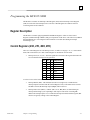
Jumper Installation
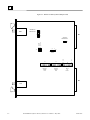
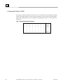
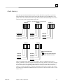
Figure 2-1 on page 2-4 shows the layout of jumpers on the Reflective Memory Board.
J-4 and J-7 are address jumpers. These jumpers must be set to the desired base address of the board
as described in “Extended Address Field (J4)”, “Address Pass Through Field (J7)”, and “Standard
Address Match Field (J7)”.
J3, J5, J8, and J9 must be set to configure other functions of the board as described in “Board Node
ID Field (J9)”, “Address Modifier Select (J8)”, “Fast Field (J5)”, and “Mask Field (J3)” on page 211.
GFK-2054
Chapter 2 Configuration and Installation
2-3
2
Figure 2-1: Reflective Memory Board Jumper Fields
XMIT
MEM DEPTH 1
MEM DEPTH 2
J1
J2
A4
A3
A2
A1
P1
STD/EXTD
ADDRESS SEL
J10
M
A
S
K
F
A
S
T
S
P
A
R
E
1
2
3
J3
J8
Address Mode
Select.
Extended
Address
Field
ID1
ID2
ID3
ID4
ID5
J9
ID6
A18
A19
A20
A21
A22
AP19
AP18
A24
A26
A25
A23
Standard
Address
Field
L
S
B
ID0
M
S
B
J7
A27
A28
A29
A31
A30
J4
ID7
J5 J6
Board
ID
Nodes
P2
RCV
2-4
IC697VRM015 Reflective Memory Board User’s Manual – May 2002
GFK-2054
2
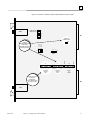
Extended Address Field (J4)
If the extended address jumper, J10, is installed, the extended address match field becomes active.
The extended address field selects A31 through A24. An installed jumper is a logic low and no
jumper is a logic "one". Refer to Figure 2-2 on page 2-6 and Figure 2-3 on page 2-7.
Address Pass Through Field (J7)
J1 and J2 are configured at the factory and should not need configuration by the user. The
information in the rest of this paragraph is for reference only. Refer to Figure 2-4 on page 2-8.
Standard Address Match Field (J7)
The standard address match field is always active. An installed jumper indicates a logic "zero"
address. The Active field is as follows:
256 K:
GFK-2054
(A23 through A18)
Chapter 2 Configuration and Installation
2-5
2
Figure 2-2: Reflective Memory Board Extended Address Jumper Fields
MEM DEPTH 1
MEM DEPTH 2
XMIT
J1
J2
A4
A3
A2
A1
P1
STD/EXTD
ADDRESS SEL
J10
M
A
S
K
F
A
S
T
S
P
A
R
E
1
2
3
J3
J8
Address Mode
Select.
Extended
Address
Field
Standard
Address
Field
ID1
ID2
ID3
ID4
ID5
ID0
L
S
B
J9
ID6
A18
A19
A20
A21
A22
A23
AP19
AP18
A24
J7
A26
A25
A27
A28
A29
J4
A31
A30
JUMPER
ARRANGEMENT TO
CONFIGURE
EXTENDED ADDRESS
$5AXXXXXX HEX
M
S
B
ID7
J5 J6
Board
ID
Nodes
P2
RCV
2-6
IC697VRM015 Reflective Memory Board User’s Manual – May 2002
GFK-2054
2
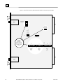
Figure 2-3: Reflective Memory Board Standard Address Jumper Fields
XMIT
MEM DEPTH 1
MEM DEPTH 2
J1
J2
A4
A3
A2
A1
P1
STD/EXTD
ADDRESS SEL
J10
MF
A A
S S
K T
S
P
A
R
E
1
2 3
J3
J8
Address Mode
Select.
Extended
Address
Field
NOTE THAT FOR
STANDARD
ADDRESSES
THIS JUMPER FIELD
IS A DON’T CARE!
Standard
Address
Field
ID1
ID2
ID3
ID4
ID5
ID0
L
S
B
J9
ID6
A18
A19
A20
A21
A23
AP19
AP18
A24
A25
J7
A26
A27
A28
A29
A31
A30
J4
M
S
B
ID7
J5 J6
A22
JUMPER
ARRANGEMENT TO
CONFIGURE
EXTENDED ADDRESS
$XX9XXXXX HEX
Board
ID
Nodes
P2
RCV
GFK-2054
Chapter 2 Configuration and Installation
2-7
2
Figure 2-4: Reflective Memory Board Extended Address with 256 Kbyte Example
XMIT
MEM DEPTH 1
MEM DEPTH 2
J1
J2
A4
A3
A2
A1
P1
STD/EXTD
ADDRESS SEL
J10
F
A
S
T
1
2
3
J8
J3
Address Mode
Select.
Extended
Address
Field
ID1
ID2
ID3
ID4
ID5
J9
ID6
A18
A19
A20
AP18
AP19
A24
A25
A26
A23
Standard
Address
Field
L
S
B
ID0
M
S
B
J7
A27
A28
A29
A30
A31
J4
A21
JUMPER
ARRANGEMENT TO
CONFIGURE
EXTENDED ADDRESS
$5A9 4 XXXX HEX WITH
1/4 MEGABYTE RAM
OPTION
ID7
J5 J6
A22
M
A
S
K
S
P
A
R
E
Board
ID
Nodes
P2
RCV
2-8
IC697VRM015 Reflective Memory Board User’s Manual – May 2002
GFK-2054
2
Board Node ID Field (J9)
The Board Node ID field identifies each board on the Memory link. No ID may be used more than
once on the link. All nodes on the link should be sequentially numbered starting with 0. Jumper
field J9, provides a double hexadecimal digit defining the board node ID. An installed jumper sets
the corresponding bit to 0. There is no relation between node number and physical position on the
link. Nodes may be physically located in any order. Refer to Figure 2-8 on page 2-12.
Address Modifier Select (J8)
The Reflective Memory Board may operate in one of three modes: supervisory data access,
nonprivileged data access, or both. The different options are shown in Figure 2-7 below and Figure
2-9 on page 2-13.
Figure 2-7: Address Modifier Jumper Options
J8
1
J8
3
3
1
BOTH
J8
NONPRIVILEGED
1
3
SUPERVISORY
Fast Field (J5)
If the J5 jumper is left off the fiber-optic link rate is 6.2 Mbytes. If the jumper is present, the link
rate is 3.2 Mbytes. The 3.2 Mbytes rate results from transmitting every data word twice. If an error
is detected in the first transmission, it is thrown away and the second transmission of data is used.
If the first transmission is OK, the second is ignored.
Mask Field (J3)
If the mask jumper is present, the INT0 on the MC68153 interrupt IC is set when a data error is
detected. The CSR can be read to determine if the INT0 was set by the transmitter becoming halffull or by a transfer error. If the mask jumper is removed then no interrupt is generated. In
redundant transfer mode, the user does not care if a transfer error occurs on a single transfer since
the second transfer statistically is certain to be received correctly. The CSR bit 3 is always set if a
single transfer error is detected regardless of the state of the mask jumper.
Spare Field (J6)
Not used.
GFK-2054
Chapter 2 Configuration and Installation
2-9
2
Figure 2-5: Reflective Memory Board Board Node ID Jumper Field
XMIT
MEM DEPTH 1
MEM DEPTH 2
J1
J2
A4
A3
A2
A1
P1
STD/EXTD
ADDRESS SEL
J10
F
A
S
T
1
2
3
J3
J8
Address Mode
Select.
Extended
Address
Field
Standard
Address
Field
ID1
ID2
ID3
ID4
ID5
ID0
L
S
B
J9
ID6
A18
A19
A20
A21
A23
AP18
AP19
A24
A25
A26
J7
A27
A28
A29
A30
A31
J4
M
S
B
ID7
J5 J6
A22
JUMPER
ARRANGEMENT TO
CONFIGURE A
BOARD NODE ID OF
$07 HEX
M
A
S
K
S
P
A
R
E
Board
ID
Nodes
P2
RCV
2-10
IC697VRM015 Reflective Memory Board User’s Manual – May 2002
GFK-2054
2
Figure 2-6: Reflective Memory Board Address Modifier Jumper Field
XMIT
MEM DEPTH 1
MEM DEPTH 2
J1
J2
A4
A3
A2
A1
P1
STD/EXTD
ADDRESS SEL
J10
M
A
S
K
F
A
S
T
S
P
A
R
E
1
2
3
J3
J8
Address Mode
Select.
Extended
Address
Field
ID1
ID2
ID3
ID4
ID5
J9
ID6
A18
A19
A20
A21
A22
AP18
AP19
A24
A25
A23
Standard
Address
Field
L
S
B
ID0
M
S
B
J7
A26
A27
A28
A29
A30
J4
A31
JUMPER
ARRANGEMENT TO
CONFIGURE BOTH
SUPERVISORY AND
NONPRIVILEGED
DATA ACCESS
ID7
J5 J6
Board
ID
Nodes
P2
RCV
GFK-2054
Chapter 2 Configuration and Installation
2-11
2
Fiber-Optic Link Configuration
A link of the Reflective Memory Board is formed by connecting the transmit of Card A into the
receiver of Card B. Card B’s transmitter is then connected to the receiver of Card C and so on. The
last card in the link has its transmit connected back to Card A receiver to close the link.
When data has been sent around the link and returns to the originating node, two things happen.
One, the data is removed from the link. This is done by comparing an ID tag sent with data to the
local node ID. If a match is determined, the data is removed. The second event which occurs is that
the OWN-ID bit is set in the CSR. Loop data latency can be measured by writing a "zero" to the
OWN-ID bit in the CSR and polling until it returns to a "one" state. This test assumes there is no
other data originated by the local node on the link before the latency test is initiated. The data write
to the CSR is passed around the link as regular traffic but will not affect the status of any other
nodes CSR. The CSR data write provides a means to measure latency without giving up any
memory which may be in use in order to measure data transfer latency.
If data was not generated by the local node, it is placed in the receive FIFO. The receive FIFO then
places data in RAM and into the transmit FIFO to be sent to the next node on the link. Data can be
mixed from the local VME and the link based on which arrives at what time. Just because two data
transfers arrive in one node back-to-back does not guarantee a transfer cannot be inserted between
them by the local VME card.
Priority is given to the local VME card in case of a simultaneous access to the RAM and the
transmit FIFO by the local VME and the receive FIFO. In any other case, the other must wait for
the current cycle to finish to gain access to the RAM.
2-12
IC697VRM015 Reflective Memory Board User’s Manual – May 2002
GFK-2054
2
IACK Daisy Chain
If there are empty slots to the left of the Reflective Memory Board, then IACK Jumpers must be
installed for the empty slots. Otherwise, the Reflective Memory Board will intermittently fail to
respond to VMEbus reads and writes.
GFK-2054
Chapter 2 Configuration and Installation
2-13
Chapter
Programming
3
This chapter contains programming instructions for the Reflective Memory Board, and is divided
into the following sections:
GFK-2054
Introduction to Controlling the Reflective Memory Board
Board Identification (ID) Register
Node ID Register
Board Control and Status Register (CSR)
Programming the MC68153 BIM
The Command Register Definition (06H)
Command Node (07H)
Interrupt Sender ID Registers (26H, 2AH, 2EH)
Local Status Interrupt
3-1
3
Introduction to Controlling the Reflective Memory Board
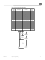
Although the Reflective Memory Board is software transparent on power-up, some registers are
present to facilitate user information and interrupt generation. Table 3-1 on page 3-3 shows the
memory mapped registers used by the Reflective Memory Board.
3-2
IC697VRM015 Reflective Memory Board User’s Manual – May 2002
GFK-2054
3
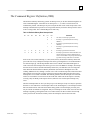
Table 3-1: Reflective Memory Board Memory Map
Relative
Address
(HEX)
Description
Contents
WriteRead
Mode
01
Board ID
ID (18 H)
Byte (R)
04
Node ID
Node No.
Byte (R)
05
CSR
Status Flags
Byte (R/W)
06
CMD Register
Interrupt Address
Byte (W)
07
CMD Node
Node to get Interrupt
Byte (R/W)
23
INT0 Mode Control
(MC68153 BIM)
Byte (R/W)
26
INT1 Sender ID
Node ID of INT1 Sender
Byte (R/W)
27
INT1 Mode Control
(MC68153 BIM)
Byte (R/W)
2A
INT2 Sender ID
Node ID of INT2 Sender
Byte (R/W)
Byte (R/W)
2B
INT2 Mode Control
(MC68153 BIM)
2E
INT3 Sender ID
Node ID of INT3 Sender
Byte (R/W)
2F
INT3 Mode Control
(MC68153 BIM)
Byte (R/W)
33
INT0 Vector
(MC68153 BIM)
Byte (R/W)
37
INT1 Vector
(MC68153 BIM)
Byte (R/W)
3B
INT2 Vector
(MC68153 BIM)
Byte (R/W)
3F
INT3 Vector
(MC68153 BIM)
Byte (R/W)
40
RAM
SRAM
All Modes
(Byte, Word,
Lword) R/W
1/4 M
03FFFF
1/2 M
07FFFF
1M
FFFFF
GFK-2054
Chapter 3 Programming
3-3
3
Board Identification (ID) Register
The Board ID Register allows the user to verify the presence of the Reflective Memory Board at
the correct address. The Reflective Memory Board ID number is $18 HEX.
3-4
IC697VRM015 Reflective Memory Board User’s Manual – May 2002
GFK-2054
3
Node ID Register
A value from 0 to 255 can be read from this byte. The value read corresponds to the node ID
jumper selected for the board.
GFK-2054
Chapter 3 Programming
3-5
3
Board Control and Status Register (CSR)
The CSR contains local node state information. The CSR is mapped as follows:
Bit 07
Bit 06
Bit 05
Bit 04
Bit 03
Bit 02
Bit 01
Bit 00
LED
RCV
Half-full
TX
Half-full
TX Empty
Bad Data
Own Data
Mask
Fast
Board Control and Status Register Bit Definitions
3-6
Bit 07:
LED – Fail LED Status (Read/Write) logic 1 = LED ON, logic 0 = LED OFF
Bit 06:
RCV Half-full – Receive FIFO half-full at least half-full when low (Read Only). This
bit displays current status of the receive FIFO. This bit should never be low. If this bit
goes low, local VME access should be suspended or at least curtailed for a period of
time or data loss could occur. This bit going low would be an indication of a local VME
problem, i.e., extremely slow release of data strobes after DTACK. In a proper
functioning VME system, this should never occur.
Bit 05:
TX Half-full – Transmit FIFO half-full - over half-full when low (Read Only). These
two bits display status on the transmit FIFO on the local node. The current status of the
transmit status is displayed.
Bit 04:
TX Empty – Transmit FIFO empty - empty when low (Read Only)
Bit 03:
Bad Data – Bad-data (high if error occurred) (Read/Write). This bit indicates that a
single transfer error has occurred. It does not depend on the mask jumper to be removed.
In redundant transmission mode (3.2 Mbytes/sec), it indicates only that a transfer error
occurred on one of the two transfers.
Bit 02:
Own Data – Own-data (high if link intact) (Read/Write). This bit indicates that the local
node has received data back that had originated on the local node. It may be reset by
writing this bit to a logic "zero". Once set by receiving its own node ID from the fiberoptic receiver, the bit remains set until cleared by the local VME side.
Bit 01:
Mask – Mask Transfer Error Interrupt Masks on high (Read Only) If the mask jumper
J3 is installed and INT0 is enabled by software on the bus interrupt module, an interrupt
will be generated each time a receive error is detected on the fiber-optic link.
Bit 00:
Fast – Fast mode (6.2 Mbytes/sec) if high (Read Only). Fast mode transmits each data
transfer once on the fiber-optic link. If the jumper J5 is installed, each transfer is sent
twice on the fiber-optic link (3.2 Mbytes/sec).
IC697VRM015 Reflective Memory Board User’s Manual – May 2002
GFK-2054
3
Programming the MC68153 BIM
The MC68153 contains one Interrupt Control Register (ICR) and one Interrupt Vector Register
(IVR) for each of the four interrupt sources. All four Control Registers are identical. All four
Vector Registers are also identical.
Register Description
The MC68153 contains eight programmable Read/Write Registers. There are four Control
Registers (CRINT0 through CRINT3) that govern operation of the device. The other four (VRINT0
through VRINT3) are Vector Registers that contain the vector data used during an interrupt
acknowledge cycle.
Control Registers (23H, 27H, 2BH, 2FH)
There is a Control Register for each interrupt source, see table 3-4 on page 3-12, i.e., CR0 controls
INT0, CR1 controls INT1, etc. Each Control Register is divided into several fields:
•
Interrupt level (L2, L1, L0) - The least significant 3-bit field of the register determines the
level at which an interrupt will be generated:
L2
L1
L0
IRQ LEVEL
0
0
0
DISABLED
0
0
1
IRQ1
0
1
0
IRQ2
0
1
1
IRQ3
1
0
0
IRQ4
1
0
1
IRQ5
1
1
0
IRQ6
1
1
1
IRQ7
A value of "zero" in the field disables the interrupt.
GFK-2054
•
Interrupt Enable (IRE) - This field (Bit 4) must be set (high level) to enable the bus
interrupt request associated with the Control Register. Thus, if the INTX line is asserted
and IRE is cleared, no interrupt request (IRQX) will be asserted.
•
Interrupt Auto-Clear (IRAC) - If IRAC (Bit 3) is set, IRE (Bit 4) is cleared during an
interrupt acknowledge cycle responding to this request. This action of clearing IRE
disables the interrupt request. To re-enable the interrupt associated with this register, IRE
must be set again by writing to the Control Register.
Chapter 3 Programming
3-7
3
•
External/Internal (X/IN) - Bit 5 of the Control Register determines the response of the
MC68153 during an interrupt acknowledge cycle. If the X/IN bit is clear (low level) the
BIM will respond with vector data and a DTACK signal, i.e., an internal response, If X/IN
is set, the vector is not supplied and no DTACK is given by the BIM, i.e., an external
device should respond. Always set to "zero" for the Reflective Memory Board.
•
Flag (F) - Bit 7 is a flag that can be changed without affecting chip operation.
•
Flag Auto-Clear (FAC) - If FAC (Bit 6) is set, the Flag bit is automatically cleared during
an interrupt acknowledge cycle.
Vector Registers (33H, 37H, 3BH, 3FH)
Each interrupt input has its own associated Vector Register (see Table 3-5 on page 3-13). Each
register is eight bits wide and supplies a data byte during its interrupt acknowledge cycle if the
associated External/Internal (X/IN) Control Register bit is clear ("zero"). This data can be status,
identification, or address information depending on system usage. The information is programmed
by the system user.
Device Reset
When the MC68153 is reset, the registers are set to a known condition. The Control Registers are
set to all "zeros" (low). The Vector Registers are set to $0F. This value is the MC68000 vector for
an uninitialized interrupt vector.
3-8
IC697VRM015 Reflective Memory Board User’s Manual – May 2002
GFK-2054
3
The Command Register Definition (06H)
The Reflective Memory Board may generate an interrupt in any or all other chassis through the use
of the Command Register. Valid choices for interrupts are: 1,2,3. Table 3-2 below shows all
combinations possible. The interrupts are processed just like data so all words sent previous to the
interrupt command will be present on receiving board’s memory before the interrupt will be issued
to the receiving board. The Command Register is Write only.
Table 3-2: Reflective Memory Board Interrupt Codes
D7
X
X
D6
1
0
D5
X
X
D4
X
X
D3
X
X
D2
X
X
D1
D0
0
0
0
1
1
0
1
1
X
X
X
X
Function
– not valid, no interrupt is generated
– Interrupt 1 is generated (INT level set by
CRINT1)
– Interrupt 2 is generated (INT level set by
CRINT2)
– Interrupt 3 is generated (INT level set by
CRINT3)
– Interrupt is generated in all chassis
– Interrupt is generated in chassis ID which was
written previously at relative address 07H. A
word or Lword Write can specify both interrupt
type and receiving Node ID in one transfer.
In the event of an external interrupt (i.e., INT1, INT2, INT3), the Reflective Memory Board will
prevent the loss of any subsequent interrupt of the same type through the use of a dedicated FIFO
for each interrupt type. The interrupt handler must execute a Read of the sender ID Register in
order to allow the next interrupt of the same type to be sent to the BIM. For example, an interrupt
INT1 has been sent across the link immediately followed by a second INT1. The receiving node
must determine that the Reflective Memory Board has issued an INT1 through the use of the
resulting VME INT level (0 through 7) and its vector. The second interrupt will remain in the INT1
FIFO until the receiving node executes a Read of location 26 HEX which will allow the second
interrupt INT1 to be issued to the BIM. This method guarantees that all interrupts sent on the link
will be serviced and the receiver knows the ID of the node which sent the interrupt it is currently
servicing. Only one Read per interrupt is allowed, otherwise loss of subsequent interrupts may
occur.
The three interrupt FIFOs are 512 bytes deep so up to 512 interrupts of any level may be queued in
the FIFO. A clear function is executed upon a Write to the int ID Register, so an interrupt level that
has been masked off for some time and contains many global or local interrupts previously sent,
may be cleared out without servicing them. Only new interrupts received will be serviced. Since the
interrupts originally go through the same receive FIFO as data, all data sent before the interrupt
will be present in the local node’s memory before the interrupt is issued to the local node.
GFK-2054
Chapter 3 Programming
3-9
3
Command Node (07H)
This register contains the node ID of the node to receive the interrupt sent by writing the command
register. This register must be set at the same time by using a 16-bit word write to both command
register and command node or prior to writing the command register. Table 3-3 below shows node
ID patterns.
Table 3-3: Reflective Memory Board Node IDs
D7
0
0
•
•
•
1
3-10
D6
0
0
•
•
•
1
D5
0
0
•
•
•
1
D4
0
0
•
•
•
1
D3
0
0
•
•
•
1
D2
0
0
•
•
•
1
D1
0
0
•
•
•
1
IC697VRM015 Reflective Memory Board User’s Manual – May 2002
D0
0
1
•
•
•
1
Node 0
Node 1
•
•
•
Node 255
GFK-2054
3
Interrupt Sender ID Registers (26H, 2AH, 2EH)
The three interrupt sender ID registers contain the ID of the node which originated the interrupt
currently being serviced. All data sent across the fiber-optic link is tagged with the ID of the
originating node so it may be removed from the link once it has been passed around the link one
time. The ID is stored in the appropriate register if the data word received is an interrupt. As part of
the interrupt handler software, the user must read the appropriate ID register in order to re-arm the
currently used interrupt. This process insures that all interrupts sent to the node will be processed.
The user may or may not use the ID, but it must be read as part of the interrupt handler process.
In the event that a certain interrupt has been masked off at the BIM, the FIFO for that interrupt may
be cleared by writing to the ID register for the specific interrupt level before the BIM is armed. The
ID write process is to be done in addition to the BIM arming process. In the interrupt handling
sequence, the user should do only one read per interrupt cycle. Erroneous results will be caused by
multiple reads.
GFK-2054
Chapter 3 Programming
3-11
3
Local Status Interrupt
The fourth interrupt on the MC68153 (INT0) is dedicated to generate an interrupt in the event that
the local FIFOs become half-full or a corrupt transfer has been received. If the interrupt is not
disabled, every time the local Reflective Memory Board is written to and the transmit FIFO is over
half full or a transfer error occurs, an INT0 will be generated. The half-full information flag is also
available by looking at the CSR. If the transmit FIFO is allowed to become full and the FIFO half
full is set, a BERR will be generated when a Write is attempted to the Reflective Memory Board.
Table 3-4 below and Table 3-5 on page 3-13 show the architecture of MC68153 registers. The
corrupt transfer interrupt may be masked off by removing the mask jumper. This is done so the user
will not be bothered by interrupts in redundant transfer mode.
Table 3-4: BIM Register Mapping for Interrupts 0 to 3
$XX23 Control Register INT0 (INT0 – Transmit FIFO Over Half-full)
Bit 07
Bit 06
Bit 05
Bit 04
Bit 03
FLAG
FLAG
AUTO
CLEAR
VECTOR
INT
ENABLE
INT
AUTO
CLEAR
F
FAC
0=INTERNAL
1=EXTERNAL
IRE
1=AUTO
0=NO
Bit 02
Bit 01
Bit 00
INTERRUPT LEVEL
L2
L1
L0
$XX27 Control Register INT1 (INT1 – Received Interrupt from Other Nodes)
Bit 07
Bit 06
Bit 05
Bit 04
Bit 03
FLAG
FLAG
AUTO
CLEAR
VECTOR
INT
ENABLE
INT
AUTO
CLEAR
F
FAC
0=INTERNAL
1=EXTERNAL
IRE
1=AUTO
0=NO
Bit 02
Bit 01
Bit 00
INTERRUPT LEVEL
L2
L1
L0
$XX2B Control Register INT2 (INT2 – Received Interrupt from Other Nodes)
Bit 07
Bit 06
Bit 05
Bit 04
Bit 03
FLAG
FLAG
AUTO
CLEAR
VECTOR
INT
ENABLE
INT
AUTO
CLEAR
F
FAC
0=INTERNAL
1=EXTERNAL
IRE
1=AUTO
0=NO
Bit 02
Bit 01
Bit 00
INTERRUPT LEVEL
L2
L1
L0
$XX2F Control Register INT3 (INT3 – Received Interrupt from Other Nodes)
3-12
Bit 07
Bit 06
Bit 05
Bit 04
Bit 03
FLAG
FLAG
AUTO
CLEAR
VECTOR
INT
ENABLE
INT
AUTO
CLEAR
F
FAC
0=INTERNAL
1=EXTERNAL
IRE
1=AUTO
0=NO
IC697VRM015 Reflective Memory Board User’s Manual – May 2002
Bit 02
Bit 01
Bit 00
INTERRUPT LEVEL
L2
L1
L0
GFK-2054
3
Table 3-5: BIM Vector Register Mapping
$XX33 Vector Register INT0
Vector Register
V7
V6
V5
V4
V3
V2
V1
V0
V2
V1
V0
V2
V1
V0
V2
V1
V0
$XX37 Vector Register INT1
Vector Register
V7
V6
V5
V4
V3
$XX3B Vector Register INT2
Vector Register
V7
V6
V5
V4
V3
$XX3F Vector Register INT3
Vector Register
V7
GFK-2054
V6
V5
Chapter 3 Programming
V4
V3
3-13
Chapter
Theory of Operation
4
This chapter discusses the operation of the Reflective Memory Board, and is divided into the
following sections:
GFK-2054
Operational Overview
Base Address Selection
Fiber-Optic Link Speed Selection
Bus Interrupter Module (BIM)
Addressing Features
Node Latency
4-1
4
Operational Overview
The Reflective Memory Board allows up to 256 VMEbus chassis to be linked together in a
sequential fashion. Data written to any node appears in all other nodes some period of time later.
The link between the nodes is two fiber-optic cables that pass address, data, and interrupt
information between adjacent boards on the link.
The Reflective Memory Board allows a user to Read or Write the RAM address space at will. All
memory Writes are stored in SRAM on the board and also put in a FIFO to be broadcast to all other
nodes. An interrupt command may also be written to any or all chassis by writing a data word into
a specific location in RAM. The data value written dictates which node(s) will receive the interrupt.
The interrupt is sent out in the order the data was received from the VMEbus, so if a block of data
was written to the board before the interrupt command is sent, then the data will be broadcast to all
boards before the interrupt command is broadcast.
Note
If there are empty slots to the left of the Reflective Memory Board, then
IACK jumpers must be installed for the empty slots. Otherwise, the
Reflective Memory Board will intermittently fail to respond to VMEbus
reads and writes.
4-2
IC697VRM015 Reflective Memory Board User’s Manual – May 2002
GFK-2054
4
Base Address Selection
The base address of the Reflective Memory Board is jumper-selectable. Once the base address is
established, all other writes to the Reflective Memory Board will be relative to the base address.
Each node on the link may have a different base address. Only the relative offset to the base
address is passed across the link. Thus, each board on the link may have a different VMEbus
address and addressing mode.
GFK-2054
Chapter 4 Theory of Operation
4-3
4
Fiber-Optic Link Speed Selection
At full speed the link can support a 6.2 Mbyte data transfer rate. However, the high-speed serial
fiber optic’s bit error rate may result in erroneous data being transferred. A slowdown option has
been included to allow the link to be slowed down by a factor of two. VME interface response time
will not be affected by the data link slowdown. All transfer errors are detectable via parity checking
and on-board receiver error detection circuitry. The slowdown mode results from sending each data
twice. The redundant transmissions statistically lowers the probability of data corruption. The
probability of data transmission failure of both transmissions is once every three thousand years.
Redundant transmissions guarantee that all data will arrive across the link correctly. A fiber-optic
transfer error is a rare event and the board which has the receive error has the capability to notify
the local VME chassis that it has occurred. In most systems it should be preferable to operate in
single transmission mode to maintain high data throughput. In the case a retransmission request is
too slow, the double transmission mode is available.
4-4
IC697VRM015 Reflective Memory Board User’s Manual – May 2002
GFK-2054
4
Bus Interrupter Module (BIM)
To facilitate handling of interrupts, an MC68153 is used on the board. The attention interrupts
(INT1, INT2, and INT3) are used to signal an interrupt from a remote chassis. An interrupt (INT0)
may be generated when the transmit FIFO on the node being written to by the VMEbus becomes
over half full. The transmit FIFO over half full condition occurs when the local node has received
data from the local VME chassis but has not been granted permission to transmit its data on the
link. All interrupts are masked off at power-up and become enabled under program control.
GFK-2054
Chapter 4 Theory of Operation
4-5
4
Addressing Features
Not all nodes have to be configured with the same memory size. Nodes may be configured to make
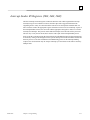
optimum use of memory. An example is shown in Figure 4-1 on page 4-7.
4-6
IC697VRM015 Reflective Memory Board User’s Manual – May 2002
GFK-2054
4
Node Latency
If the fiber-optic data bandwidth has not been exceeded, data latency is typically 1.5 µs/node in
single transfer mode. Longer latencies will result if data input rates exceed 6.2 Mbytes/sec for a
period of time. The transmit FIFOs will back up with data until the half-full interrupts are set off or
a bus error occurs in the event the FIFOs become full.
Figure 4-1: Example Memory Configurations
NODE 0
NODE 1
NODE 2
XXX00000h
X00000h
X00000h
XXX40000h
X40000h
X40000h
XXX80000h
X80000h
X80000h
XXXC0000h
XC0000h
XC0000h
NODE 3
NODE 4
Contains Memory
X00000h
X00000h
X40000h
X40000h
X80000h
X80000h
XC0000h
XC0000h
Does Not Contain Memory
Base Address of Board
Node 0 is configured with 1 Mbyte of memory, Nodes 1 and 2 are configured with 512 K of
memory, and Nodes 3 and 4 are configured with 256 K of memory. Because of the relative location
of the memory, data written to address range X00000h to X7FFFFh by a processor in Node 0 will
also be written into the corresponding address in Node 1. However, no data will be written into
Nodes 2, 3, and 4 because there is no memory in that range in those nodes. Similarly, data written
into address range X80000h to XBFFFFh in Node 2 will also be written into Nodes 0 and 3, but not
Nodes 1 and 4.
GFK-2054
Chapter 4 Theory of Operation
4-7
Chapter
Maintenance
5
This chapter provides information relative to the care and maintenance of the Reflective Memory
Board product.
If the product malfunctions, verify the following:
•
Software
•
System configuration
•
Electrical connections
•
Jumper or configuration settings
•
Boards fully inserted into their proper connector location
•
Connector pins are clean and free from contamination
•
No components of adjacent boards are disturbed when inserting or removing the board
from the VMEbus card cage
•
Quality of cables and I/O connections
User level repairs are not recommended. Contact your authorized GE Fanuc distributor for a Return
Material Authorization (RMA) Number. This RMA Number must be obtained prior to any
return.
GFK-2054
5-1
Appendix Example Code
A
This appendix contains example code for use with the Reflective Memory Board.
GFK-2054
A-1
A
/*
This code written to be down loaded into a Force CPU-33 on a VME bus.
Compiled using Cross code C compiler, using the VMIC test code library.
This file should be loaded into the 1st VME chassis CPU, setup as node
0. This routine will setup and process interrupts then report those
interrupts received. The second thing this software will do is to
attempt to fill the output fifo over half full and then process and
report that interrupt 0 occurred.
*/
#include <stdio.h>
#include <test.h>
#include "5576int.h"
/*
Declare a global pointer to the 5576 board.
*/
Vmic5576 * uut = (( Vmic5576 *)( VME_STANDARD )); /* "VME_STANDARD" defined in
VMIC Library */
/*
Declare external functions
*/
void isr_int0( void );
void isr_int1( void );
void isr_int2( void );
void isr_int3( void );
/*
global variables for the interrupt routines
*/
int int0status,int1status,int2status,int3status;
main()
{
int aa;
int0status
int1status
int2status
int3status
=
=
=
=
0xff;
0;
0;
0;
printf("\r\n\n Receive Interrupts from remote VME chassis test");
/*
**
**
**
**
**
**
**
**
**
A-2
initialize intr vector table to point to timer ISR
System dependent initialization where our system
is a Force CPU-33 Single Board Computer.
Our method of installation is via a setvect() function
that installs the interrupt service routine address in
the vector table based on the vector chosen.
IC697VRM015 Reflective Memory Board User’s Manual – May 2002
GFK-2054
A
** USER_VECTOR() is a macro in our test library that
** adds a passed value to the first available
** user vector for the Force CPU-33 interrupt table.
*/
setvect(
setvect(
setvect(
setvect(
USER_VECTOR(
USER_VECTOR(
USER_VECTOR(
USER_VECTOR(
0
1
2
3
),
),
),
),
&isr_int0
&isr_int1
&isr_int2
&isr_int3
);
);
);
);
/*
** initialize intr vector register to installed ISR
*/
uut->int0vr
uut->int1vr
uut->int2vr
uut->int3vr
=
=
=
=
USER_VECTOR(
USER_VECTOR(
USER_VECTOR(
USER_VECTOR(
0
1
2
3
);
);
);
);
/*
Clear interrupt registers of all previous interrupts
*/
uut->int1sid = 0; /* data doesn’t matter */
uut->int2sid = 0;
uut->int3sid = 0;
/*
Setup interrupt mode control registers
*/
uut->int0mc = IRQ_LEVEL_7 : INT_ENABLE; /* interrupt 0 enabled at level 7
Auto clear bit 3 low - off,
X/IN bit 5 low - internal */
uut->int1mc = IRQ_LEVEL_5 : INT_ENABLE; /* interrupt 1 enabled at level 5
Auto clear bit 3 low - off,
X/IN bit 5 low - internal */
uut->int2mc = IRQ_LEVEL_3 : INT_ENABLE; /* interrupt 2 enabled at level 3
Auto clear bit 3 low - off,
X/IN bit 5 low - internal */
uut->int3mc = IRQ_LEVEL_1 : INT_ENABLE; /* interrupt 3 enabled at level 1
Auto clear bit 3 low - off,
X/IN bit 5 low - internal */
printf("\r\n**** Setup waiting on interrupts from node 1."
"\r\nHit any key to continue after sending interrupts\r\n");
getc();
printf("int0 status = %x, int1 = %x, int2 = %x,"
"int3 = %x",int0status,int1status,int2status,int3status);
printf("\r\n\n int1 - int3 should = number of node sending interrupt");
printf("\r\n\n ***** sending data to Reflective Memory"
"\r\n
to generate transmit half full interrupt 0");
for(aa = 0;aa < 0xfaaaaa;aa += 1)
{
uut->mem5576 = 0xaa;
uut->mem5576 = 0xaa;
uut->mem5576 = 0xaa;
uut->mem5576 = 0xaa;
}
GFK-2054
Appendix A Example Code
A-3
A
printf("\r\nint0 status = %x, int1 = %x, int2 = %x,"
"int3 = %x",int0status,int1status,int2status,int3status);
printf("\r\nint0 should be f4 hex, Hit any key to continue");
getc();
printf("\r\n\n ***** sending interrupts 1,2,3 to node 1.");
for (aa = 1;aa < 4;aa += 1)
{
uut->cmdnd = 0x01;
/* node one into register 0x07 */
uut->cmdreg = aa;
/* Send interrupts 1,2,3 to node in reg. 0x07 */
}
printf("\r\n\nProgram complete");
}
#pragma interrupt()
void isr_int0( void )
{
int0status = uut->csr;
/* wait for transmit fifo to clear. */
do{
}while( ( uut->csr & TXFIFO_UHF) == 0 );
}
#pragma interrupt()
void isr_int1( void )
{
int1status = uut->int1sid; /* read id reg. to clear the interrupt. */
}
#pragma interrupt()
void isr_int2( void )
{
int2status = uut->int2sid; /* read id register to clear the interrupt. */
}
#pragma interrupt()
void isr_int3( void )
{
int3status = uut->int3sid; /* read id register to clear the
interrupt. */
}
A-4
IC697VRM015 Reflective Memory Board User’s Manual – May 2002
GFK-2054
A
/*
This is the header file for the VMIVME-5576 Reflective Memory Board
Interrupt test. This file assumes the 2 boards are -200 option.
Both VMIVME-5576 boards are jumpered for Standard Either Mode access.
*/
struct vmivme_5576 {
union reg_5576 {
unsigned char reg_5576_b[64]; /* register space */
unsigned short reg_5576_w[32];
unsigned int
reg_5576_l[16];
} r5576u;
unsigned char vmivme_5576_mem[1048512];
};
typedef struct vmivme_5576 Vmic5576;
/* 5576 type define */
/* register definitions */
#define
#define
#define
#define
#define
#define
#define
#define
#define
#define
#define
#define
#define
#define
#define
#define
#define
bid
r5576u.reg_5576_b[0x01] /* Board ID */
nid
r5576u.reg_5576_b[0x04] /* Node ID */
csr
r5576u.reg_5576_b[0x05] /* Control & Status Register */
cmdreg
r5576u.reg_5576_b[0x06] /* Command register */
cmdnd
r5576u.reg_5576_b[0x07] /* Command node */
int0mc r5576u.reg_5576_b[0x23] /* interrupt 0 mode
control register */
int0vr r5576u.reg_5576_b[0x33] /* interrupt 0
vector register */
int1sid r5576u.reg_5576_b[0x26] /* interrupt 1 sender
ID register */
int1mc r5576u.reg_5576_b[0x27] /* interrupt 1 mode
control register */
/* interrupt 1
int1vr r5576u.reg_5576_b[0x37]
vector register */
int2sid r5576u.reg_5576_b[0x2a] /* interrupt 2 sender
ID register */
int2mc r5576u.reg_5576_b[0x2b] /* interrupt 2 mode
control register */
int2vr r5576u.reg_5576_b[0x3b] /* interrupt 2
vector register */
int3sid r5576u.reg_5576_b[0x2e] /* interrupt 3 sender
ID register */
int3mc r5576u.reg_5576_b[0x2f] /* interrupt 3 mode
control register */
int3vr r5576u.reg_5576_b[0x3f] /* interrupt 3
vector register */
mem5576 vmivme_5576_mem[0x0]
/* memory */
/* Control Status Register bit define’s */
#define
#define
#define
#define
#define
#define
#define
#define
/*
GFK-2054
FAIL_LED
RXFIFO_UHF
TXFIFO_UHF
TXFIFO_NOT_EMPTY
BAD_DATA
OWN_DATA
ERR_INT_MASK
FAST
command register bit def’s
Appendix A Example Code
0x80
0x40
0x20
0x10
0x08
0x04
0x02
0x01
/* receive fifo under half full */
/* Transmit fifo under half full */
*/
A-5
A
#define
#define
#define
#define
/*
GLOBAL_INT
INT_1
INT_2
INT_3
0x40
0x01
0x02
0x03
bim control bits (for regs. int0mc-int3mc) */
#define
#define
#define
#define
#define
#define
#define
#define
#define
#define
#define
#define
#define
FLAG_BIT
FLAG_AUTO_CLR
EXT_VECTOR
INT_ENABLE
INT_AUTO_CLR
IRQ_LEVEL_7
IRQ_LEVEL_6
IRQ_LEVEL_5
IRQ_LEVEL_4
IRQ_LEVEL_3
IRQ_LEVEL_2
IRQ_LEVEL_1
INT_DISABLE
0x80
0x40
0x20
0x10
0x08
0x07
0x06
0x05
0x04
0x03
0x02
0x01
0x00
#define
MEM_OFF
0x40
/* set to 0 for internal operation */
/* Board ID register value */
#define
ID_5576
0x18
/* Interrupt FIFO depth in bytes */
#define
INT_FIFO_DEPTH
512
/* Base address pointers */
/*
Reg5578 * regbase_5578 = ((Reg5578 *)(VME_STANDARD + reg_off));*/ /* registers *
/
/*
Memory * membase_5578 = ((Memory *)(VME_STANDARD + mem_off));*/
/
A-6
IC697VRM015 Reflective Memory Board User’s Manual – May 2002
/* memory *
GFK-2054
Appendix Troubleshooting Guide
B
This chapter contains troubleshooting information for the Reflective Memory Board.
GFK-2054
B-1
B
Symptom
Card/Cards bus error
when accessed after
multiple writes
Possible Cause
1.
IACKIN/IACKOUT daisy chain not in place on one or more
nodes on network. (IACKIN must be in place on the backplane
even if interrupts are not used on the node)
2.
The local node ID is higher than the maximum node ID
strapped on Node 0.
3.
System throughput has reached maximum and FIFO’s have
filled up with data to be sent and the transmit FIFO half-full
signal has been ignored.
4.
P3/P4 cable swapped or lines are open between cable and local
node.
5.
No Node 0 present to pass token.
Communications lost after
power down and up of one
or more Nodes on link
1.
Receive FIFO’s on one or more nodes have been ’glitched’ by
an out of spec txclk on link. Reset all nodes or issue link reset
to nodes strapped to listen to the link reset signal.
Erratic communications on
data link
1.
Link rate too high for cable length. i.e.,
Rate
1 (20 MBYTE/SEC)
2 (10 MBYTE/SEC)
3 (5 MBYTE/SEC)
4 (2.5 MBYTE/SEC)
Node does not answer at
expected address
B-2
Max Length
50’
100’
250’
1000’
2.
Open cable at one or more pins on link.
3.
Terminator resistors not installed on end nodes of link or extra
terminators have been left on center nodes.
4.
P3/P4 pins pushed back on Node connector. Inspect pins for
damage.
5.
P3/P4 cable has crushed pin in Panduit connector. Try
swapping P3 cable to P4 and P4 cable to P3 on all nodes. If
symptoms of problem change, at least one of the cables is bad.
1.
Address pass through for specific memory size not strapped
correctly. (See Chapter 2, “Configuration and Installation.”)
2.
Address modifier incorrectly strapped on card
3.
Address strapped wrong. (Certain LSB address jumpers must
be left off because of memory size options).
IC697VRM015 Reflective Memory Board User’s Manual – May 2002
GFK-2054
B
Symptom
Data written to one node
does not appear in other
nodes
1.
For nodes of memory size 1 MBYTE or smaller, a 1 MBYTE
relative address is nodes passed. If two 0.25 MBYTE cards are
not mapped in the same relative address in relation to the 1
MBYTE boundary, then they will not appear to communicate
since they contain no common space in RAM. The 2 and 4
MBYTE cards pass a 4 MBYTE relative address and thus must
be mapped in the same address relative to 4 MBYTE
boundaries. (Note that 4 and 2 MBYTE nodes may not be used
on the same link as 1 MBYTE or smaller nodes due to the fact
that they look at different relative address sizes)
2.
The sending node ID is higher than the maximum node ID
strapped on Node 0.
3.
Open or defective connection to cable P3 or P4.
4.
Defective FIFO module on either receiving node or
transmitting node. (The bad card may be found by checking
memory on other nodes to see if they received data correctly.)
Receive FIFO fills up and
never empties out even
after link traffic stops
1.
IACKIN has not been connected to the interrupt Arbiter card.
(VME Slot 0 card.)
Data Bits dropped or data
appears in wrong address
in memory
1.
Damaged or defective FIFO on node.
2.
Link rate set too high for cable length.
3.
Damaged cable or connector to link.
1.
Possible write to same memory location in two or more cards
at the same time. (This must be prevented in software.)
2.
Damaged local node.
3.
Link rate set too high for cable length.
4.
Damaged cable or connection on node with data error.
1.
IACKIN is not daisy chained from the CPU to the reflective
memory card on the backplane. VME spec requires all empty
VME slots to have IACKIN jumpered to IACKOUT.
Reflective memory cards expect IACKIN to be driven even if
interrupts are not being used.
2.
The IACKIN/IACKOUT jumper has been placed on backplane
for the slot the reflective memory is residing in. This shorts the
IACKOUT driver in the previous slot to the reflective memory
IACKOUT driver.
If data is wrong in a node
and is correct in all other
nodes
When interrupts are being
used, a spurious interrupt
is issued from the CPU
GFK-2054
Possible Cause
Appendix B Troubleshooting Guide
B-3