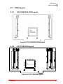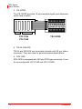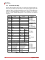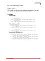
1
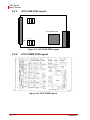
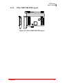
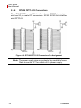
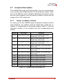
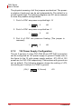
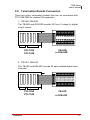
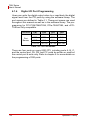
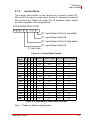
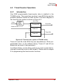
72XX Series 24/48/96-CH Digital I/O Card User’s Manual Manual Revision: 2.61 Revision Date: July 4, 2009 Part Number: 50-11104-2020 Advance Technologies; Automate the World. 72XX Series User’s Manual ii 72XX Series User’s Manual Table of Contents Table of Contents................................................................... iii List of Figures ....................................................................... vii List of Tables.......................................................................... ix 1 Introduction ........................................................................ 1 1.1 Features............................................................................... 2 1.1.1 Digital I/O Ports..................................................................... 2 1.1.2 Timer/Counter and Interrupt System .................................... 2 1.1.3 Miscellaneous ....................................................................... 2 1.2 Applications ......................................................................... 2 1.3 Specifications....................................................................... 3 1.4 Software Support ................................................................. 5 1.4.1 Programming Library ............................................................ 5 2 Installation .......................................................................... 7 2.1 What You Have.................................................................... 7 2.2 Unpacking............................................................................ 8 2.3 PCB Layout.......................................................................... 9 2.3.1 PCI-7248/7224 PCB Layout ................................................ 9 2.3.2 PCI-7296 PCB Layout ......................................................... 9 2.3.3 cPCI-7248 PCB Layout ...................................................... 10 2.3.4 cPCI-7249R PCB Layout ................................................... 10 2.3.5 PCIe-7248/7296 PCB Layout ............................................. 11 2.4 Hardware Installation ......................................................... 12 2.4.1 PCI configuration ................................................................ 12 2.4.2 PCI/PCI Express slot selection ........................................... 12 2.5 Device Installation for Windows Systems .......................... 13 2.6 Connector Pin Assignment ................................................ 14 2.6.1 PCI-7224/7248/7296 & PCIe-7248/7296 Pin Assignment .. 14 Table of Contents iii 72XX Series User’s Manual 2.6.2 cPCI-7248 Pin Assignment ................................................. 16 2.6.3 cPCI-7249R Pin Assignment .............................................. 17 2.6.4 R7249 OPTO-22 Connectors.............................................. 18 2.7 Jumpers Description .......................................................... 19 2.7.1 Power on Status of Ports .................................................... 19 2.7.2 12V Power Supply Configuration ........................................ 20 2.8 Termination Boards Connection ........................................ 21 3 Registers Format .............................................................. 23 3.1 PCI Plug and Play Registers.............................................. 23 3.2 I/O Address Map ................................................................ 24 4 Operation Theory .............................................................. 25 4.1 Digital I/O Ports.................................................................. 25 4.1.1 Introduction ......................................................................... 25 4.1.2 8255 Mode 0 ....................................................................... 25 4.1.3 Special Function of the DIO Signals ................................... 25 4.1.4 Digital I/O Port Programming .............................................. 26 4.1.5 Control Word....................................................................... 27 4.1.6 Power On Configuration...................................................... 28 4.1.7 Note for Output Data........................................................... 28 4.1.8 Note for cPCI-7249R........................................................... 28 4.2 Timer/Counter Operation ................................................... 29 4.2.1 Introduction ......................................................................... 29 4.2.2 General Purpose Timer/Counter......................................... 30 4.2.3 Cascaded 32 Bits Timer...................................................... 30 4.2.4 Event Counter and Edge Control ........................................ 30 4.3 Interrupt Multiplexing.......................................................... 31 4.3.1 Architecture......................................................................... 31 4.3.2 IRQ Level Setting................................................................ 31 4.3.3 Note for Dual Interrupts....................................................... 32 4.3.4 Interrupt Source Control...................................................... 32 iv Table of Contents 72XX Series User’s Manual 4.4 12V and 5V Power Supply................................................. 34 5 C/C++ Libraries................................................................. 35 5.1 Libraries Installation........................................................... 35 5.2 Programming Guide........................................................... 36 5.2.1 Naming Convention ............................................................ 36 5.2.2 Data Types ......................................................................... 36 5.3 _7248/96_Initial ................................................................. 37 5.4 Digital Input........................................................................ 39 5.5 Digital Output ..................................................................... 42 5.6 Configuration Port.............................................................. 43 5.7 Configuration Channel ....................................................... 45 5.8 Set Interrupt Control .......................................................... 47 5.9 Timer Start ......................................................................... 49 5.10 Timer Read ........................................................................ 50 5.11 Timer Stop ......................................................................... 51 5.12 Cascaded Timer ................................................................ 52 5.13 Get IRQ Status .................................................................. 53 5.14 Clear IRQ........................................................................... 55 5.15 Software Reset .................................................................. 56 5.16 Interrupt Start under Windows ........................................... 57 5.17 Interrupt Stop under Windows ........................................... 59 Table of Contents v 72XX Series User’s Manual This page intentionally left blank. vi Table of Contents 72XX Series User’s Manual List of Figures Figure 2-1: Figure 2-2: Figure 2-3: Figure 2-4: Figure 2-5: Figure 2-6: Figure 2-7: Figure 2-8: Figure 4-1: Figure 4-2: Figure 4-3: PCI-7248/7224 PCB Layout ............................................ 9 PCI-7296 PCB Layout ..................................................... 9 cPCI-7248 PCB Layout.................................................. 10 cPCI-7249R Layout ....................................................... 10 PCIe-7248/7296 PCB Layout ........................................ 11 Pin assignments and power signals of PCI/PCIe-7224/7248/7296............................................. 14 Pinout and power signals of cPCI-7248......................... 16 R7249 OPTO-22 Connectors Pin Assignment .............. 18 Control Word Format ..................................................... 27 Timer/counter system of 7248/96 series........................ 29 Dual Interrupt System of PCI-7224/7248/96.................. 31 List of Figures vii 72XX Series User’s Manual This page intentionally left blank. viii List of Figures 72XX Series User’s Manual List of Tables Table Table Table Table Table Table Table 2-1: 3-1: 4-1: 4-2: 4-3: 4-4: 5-1: List of Tables Jumpers and Port names list ......................................... 19 I/O Address Map............................................................ 24 I/O Port Names .............................................................. 26 Summary of control word (D0-D4) ................................. 27 ISC register format......................................................... 33 IRQ Trigger conditions................................................... 33 Data Types .................................................................... 36 ix 72XX Series User’s Manual This page intentionally left blank. x List of Tables 72XX Series User’s Manual Preface Copyright 2009 ADLINK TECHNOLOGY INC. This document contains proprietary information protected by copyright. All rights are reserved. No part of this manual may be reproduced by any mechanical, electronic, or other means in any form without prior written permission of the manufacturer. Disclaimer The information in this document is subject to change without prior notice in order to improve reliability, design, and function and does not represent a commitment on the part of the manufacturer. In no event will the manufacturer be liable for direct, indirect, special, incidental, or consequential damages arising out of the use or inability to use the product or documentation, even if advised of the possibility of such damages. Trademarks Borland® C/C++ and Delphi® are registered trademarks of the Borland Software Corporation. Intel® is a registered trademark of Intel Corporation. LabVIEW™ is a trademark of National Instruments Corporation. Linux® and the Linux® Logo are registered trademarks of Linus Torvalds. MATLAB® and the MATLAB Logo are registered trademarks of The MathWorks, Inc. Microsoft®, MS-DOS®, Windows® 95, Windows® 98, Windows NT®, Windows® 2000, Windows® 2003 Server®, Windows® XP, Windows Vista®, ActiveX®, Visual Studio®, Visual Basic®, Visual C#®, and Visual C++® are registered trademarks of Microsoft Corporation. PCI™, CompactPCI®, and PCI Express®, are registered trademarks of the Peripheral Component Interconnect Special Interest Group (PCI-SIG). PXI™ is a trademark of the PXI systems Alliance. VEE™ is a trademark of Agilent. Product names mentioned herein are used for identification purposes only and may be trademarks and/or registered trademarks of their respective companies. xi 72XX Series User’s Manual Getting Service Contact us should you require any service or assistance. ADLINK Technology Inc. Address: 9F, No.166 Jian Yi Road, Chungho City, Taipei County 235, Taiwan קᗼխࡉؑ৬ԫሁ 166 ᇆ 9 ᑔ Tel: +886-2-8226-5877 Fax: +886-2-8226-5717 Email: [email protected] Ampro ADLINK Technology Inc. Address: 5215 Hellyer Avenue, #110, San Jose, CA 95138, USA Tel: +1-408-360-0200 Toll Free: +1-800-966-5200 (USA only) Fax: +1-408-360-0222 Email: [email protected] ADLINK Technology Beijing Address: ࣫ҀᏖ⍋⎔ऎϞഄϰ䏃 1 োⲜ߯ࡼॺ E ᑻ 801 ᅸ (100085) Rm. 801, Power Creative E, No. 1, B/D Shang Di East Rd., Beijing 100085, China Tel: +86-10-5885-8666 Fax: +86-10-5885-8625 Email: [email protected] ADLINK Technology Shanghai Address: Ϟ⍋Ꮦⓩ⊇⋒催⾥ᡔᓔথऎ䩺∳䏃 333 ো 39 ᐶ 4 ሖ (200233) Tel: +86-21-6495-5210 Fax: +86-21-5450-0414 Email: [email protected] ADLINK Technology Shenzhen Address: ⏅ഇᏖफቅऎ⾥ᡔುफऎ催ᮄफϗ䘧᭄ᄫᡔᴃು A1 ᷟ 2 ὐ C ऎ (518057) 2F, C Block, Bld. A1, Cyber-Tech Zone, Gao Xin Ave. Sec 7, High-Tech Industrial Park S., Shenzhen, 518054 China Tel: +86-755-2643-4858 Fax: +86-755-2664-6353 Email: [email protected] xii 72XX Series User’s Manual ADLINK Technology Inc. (German Liaison Office) Address: Nord Carree 3, 40477 Duesseldorf, Germany Tel: +49-211-495-5552 Fax: +49-211-495-5557 Email: [email protected] ADLINK (French Liaison Office) Address: 15 rue Emile Baudot, 91300 MASSY Cedex, France Tel: +33 (0) 1 60 12 35 66 Fax: +33 (0) 1 60 12 35 66 Email: [email protected] ADLINK Technology Japan Corporation Address: 151-0072 ᧲੩ㇺᷦ⼱ᐈ䊱⼱㩷 1-1-2 ᦺᣣ↢ᐈ䊱⼱䊎䊦 8F Asahiseimei Hatagaya Bldg. 8F 1-1-2 Hatagaya, Shibuya-ku, Tokyo 151-0072, Japan Tel: +81-3-4455-3722 Fax: +81-3-5333-6040 Email: [email protected] ADLINK Technology Inc. (Korean Liaison Office) Address: 昢殾柢 儛單割 嚂笊壟 60-12 壟昷捒娯 4 猻 402 笾 No.402, Dongsung B/D, 60-12, Nonhyeon-Dong Gangnam-gu, Seoul, 135-010, Korea. Tel: +82-2-2057-0565 Fax: +82-2-2057-0563 Email: [email protected] ADLINK Technology Singapore Pte Ltd. Address: 84 Genting Lane #07-02A, Cityneon Design Centre, Singapore 349584 Tel: +65-6844-2261 Fax: +65-6844-2263 Email: [email protected] ADLINK Technology Singapore Pte Ltd. (Indian Liaison Office) Address: No. 1357, "Anupama", Sri Aurobindo Marg, 9th Cross, JP Nagar Phase I, Bangalore - 560078, India Tel: +91-80-65605817 Fax: +91-80-22443548 Email: [email protected] xiii 72XX Series User’s Manual This page intentionally left blank. xiv 72XX Series User’s Manual 1 Introduction The 7248/7296 series products are general purpose digital I/O cards. This series includes the following cards: PCI-7224: 24-CH PCI DIO card PCI-7248: 48-CH PCI DIO card PCI-7296: 96-CH PCI DIO card cPCI-7248: 3U CompactPCI 48-CH DIO card cPCI-7249R: 3U CompactPCI 48-CH DIO card with Rear I/O PCIe-7248: 48-CH PCI Express DIO Card PCIe-7296: 96-CH PCI Express DIO Card The 7248 series products are multi-function digital I/O boards used for industrial PCs with PCI, PCI Express, or CompactPCI buses. The cards are Plug and Play therefore it is not necessary to set any jumper for configuration of I/O address or interrupt resources. The PCI/PCIe-7248 and PCI/PCIe-7296 are 48-channel and 96channel DIO cards respectively. PCI-7224 is a reduced version of PCI-7248, where all functions are exactly the same as PCI-7248 with the exception that there are only 24 channels. The cPCI-7248 is the 3U CompactPCI version of the PCI-7248. The software is fully compatible with the PCI-7248. In this manual, if the specifications for PCI-7224, PCIe-7248/7296, and cPCI-7248 are not specified, they are the same as that of PCI-7248. The PCI/PCIe-7248 emulates two industry standard 8255 Programmable Peripheral Interface (PPI) chips operated under mode zero configuration. The PCI/PCIe-7296 emulates four PPI chips. These two cards are compatible not only on hardware connectors but also on software programming. The cPCI-7248 is the CompactPCI version of PCI-7248. All the functions are exactly the same as PCI-7248. The cPCI-7249 is an extended version of cPCI-7248, with an additional latch register and rear I/O capability. Every PPI connector has 3 ports: PA, PB, and PC. The PC can also be subdivided into 2 nibble-wide (4-bit) ports - PC Upper and Introduction 1 72XX Series User’s Manual PC Low. Each connector corresponds to one PPI chip with 24 DIO points. PCI-7224/7248/7296 are equipped with one, two, and four 50-pin male ribbon connectors respectively. The cPCI-7248 is equipped with one 100-pin SCSI-type connector. 1.1 Features The 7248/96 series products provide the following advanced features: 1.1.1 Digital I/O Ports 24/48/96 TTL/DTL compatible with digital I/O lines Emulates industry standard mode 0 of 8255 PPI Buffered circuits for higher driving Direct interface with OPTO-22 compatible I/O module Output status read-back 1.1.2 Timer/Counter and Interrupt System A 32 bits timer to generate watchdog timer interrupt A 16 bits event counter to generate event interrupt Programmable interrupt source Dual interrupt system 1.1.3 Miscellaneous Provide 12V and 5V power supply on OPTO-22 connectors On board reset-able fuses to protect power supply for external devices 1.2 Applications 2 Programmable mixed digital input & output Industrial monitoring and control Digital I/O control Contact closure, switch/keyboard monitoring Connects with OPTO-22 compatible modules Useful with A/D and D/A to implement a data acquisition and control system Introduction 72XX Series User’s Manual 1.3 Specifications I/O channels Digital Input Signal Digital Output Signal (Port A & B) Digital Output Signal (Port C) Operating Temperature Storage Temperature Humidity I/O Connectors Bus Introduction 24-bit for PCI-7224 48-bit for PCI/PCIe-7248 96-bit for PCI/PCIe-7296 48-bit for cPCI-7248 and cPCI-7249R Logic High Voltage: 2.0 V to 5.25V Logic Low Voltage: 0.0 V to 0.80V Logic High Current: 20.0 uA Logic Low Current: -0.2 mA Logic High Voltage: Minimum 2.4 V Logic Low Voltage: Maximum 0.5V Logic High Current: -2.6 mA Logic Low Current: 24.0 mA Logic High Voltage: Minimum 2.4 V Logic Low Voltage: Maximum 0.4V Logic High Current: -15.0 mA Logic Low Current: 24.0 mA 0°C - 60°C -20°C - 80°C 5% - 95% non-condensing 50-pin male ribbon cable connectors for PCI7224/7248/7296 and PCIe-7248/7296 100-pin SCSI-type connectors for cPCI-7248 PCI bus for PCI-7224/7248/7296 3U 32-bit CompactPCI Bus for cPCI-7248 x1 PCI Express for PCIe-7248/7296 3 72XX Series User’s Manual Power Consumption PCI-7224: (without external devices) 330mA @ 5VDC (Typical) 350mA @ 5VDC (Maximum) PCI-7248: 500mA @ 5VDC (Typical) 540mA @ 5VDC (Maximum) PCI-7296: 860mA @ 5VDC (Typical) 940mA @ 5VDC (Maximum) PCIe-7248: 350 mA @ 12VDC 280 mA @ 3.3VDC PCIe-7296: 590 mA @ 12VDC 280 mA @ 3.3VDC cPCI-7248: 470mA @ 5VDC (Typical) 560mA @ 5VDC (Maximum) cPCI-7249R: 700mA @ 5VDC (Typical) Transfer Rate 500 K bytes/s (Maximum) PCB Dimension PCI-7224: 148 mm x 102 mm PCI-7248: 148 mm x 102 mm PCI-7296: 166 mm x 102 mm PCIe-7248: 168 mm x 112 mm PCIe-7296: 168 mm x 112 mm cPCI-7248: 3U CompactPCI form factor cPCI-7249R: 3U CompactPCI form factor, J2 with Rear I/O option 4 Introduction 72XX Series User’s Manual 1.4 Software Support ADLINK provides versatile software drivers and packages for different approaches to building systems. We not only provide programming libraries such as DLL for many Windows systems, but also provide drivers for many software packages such as LabVIEW®, HP VEETM, MATLABTM, and many more. All the software options are included in the ADLINK CD. The nonfree software drivers are protected by serial licensed codes. Without the software serial number, the user can still install them and run the demo version for two hours for demonstration purpose. Please contact your dealer to purchase the formal license serial code. 1.4.1 Programming Library For customers who are writing their own programs, we provide function libraries for many different operating systems, including: DOS Library: Borland C/C++ and Microsoft C++, the functions descriptions are included in this user’s guide. Windows 95 DLL: For VB, VC++, Delphi, BC5, the functions descriptions are included in this user’s guide. PCIS-DASK: Include device drivers and DLL for Windows 2000/XP/Vista. DLL is binary compatible across Windows 2000/XP/Vista. In other words, all applications developed with PCIS-DASK are compatible across Windows 2000/XP/ Vista. The developing environment can be VB, VC++, Delphi, BC5, or any Windows programming language that allows calls to a DLL. The user’s guide and function reference manual of PCIS-DASK are in the CD. Please refer the PDF manual files under the following directory: \\Manual_PDF\Software\PCIS-DASK Introduction 5 72XX Series User’s Manual PCIS-DASK/X: Include device drivers and shared library for Linux. The developing environment can be Gnu C/C++ or any programming language that allows linking to a shared library. The user's guide and function reference manual of PCIS-DASK/X are in the CD. (\Manual_PDF\Software\PCIS-DASK-X.) The above software drivers are shipped with the board. Please refer to the “Software Installation Guide” to install these drivers. For additional driver support, please visit to http://www.adlinktech.com/MAPS/software-product.html. 6 Introduction 72XX Series User’s Manual 2 Installation This chapter describes how to install the 7248/96 series products. Please take note of the packing and unpacking instructions as described below: Check what you have (section 2.1) Unpacking (section 2.2) Check the PCB (section 2.3) Hardware installation (section 2.4) Device Installation for Windows System (section 2.5) Connector pin assignment (section 2.6) Jumpers setup (section 2.7) Termination boards connection (section 2.8) 2.1 What You Have In addition to this User's Manual, the package also includes: The PCI, PCI Express, or CompactPCI board ADLINK CD Software Installation Guide A DB-100RU rear I/O transition board is included in the cPCI-7249R. If any of these items are missing or damaged, please contact the dealer from whom you purchased the product. Keep the shipping materials and box in case you want to ship or store the product in the future. Installation 7 72XX Series User’s Manual 2.2 Unpacking Your card contains sensitive electronic components that can be easily damaged by static electricity. The card should be placed on a grounded anti-static mat. The operator should wear an anti-static wristband, grounded at the same point as the anti-static mat. Inspect the card module carton for obvious damage. Shipping and handling may cause damage to your module. Ensure there is no shipping and handling damage on the module before processing. After opening the card module carton, remove the system module and place only on a grounded anti-static surface with components side up. Again inspect the module for damages. Press down on all the socketed IC's to make sure they are properly seated. Only do this with the module placed on a firm flat surface. NOTE: DO NOT APPLY POWER TO THE CARD IF IT HAS BEEN DAMAGED. You are now ready to install your 7248/96 series product. 8 Installation 72XX Series User’s Manual 2.3 PCB Layout 2.3.1 PCI-7248/7224 PCB Layout Figure 2-1: PCI-7248/7224 PCB Layout 2.3.2 PCI-7296 PCB Layout PCI Controller CN1 CN2 CN3 CN4 Figure 2-2: PCI-7296 PCB Layout Installation 9 72XX Series User’s Manual 2.3.3 cPCI-7248 PCB Layout CPCI-7248 JC2 JB2 JA2 PCI Controller Chip JA1 JB1 JC1 CN1 Figure 2-3: cPCI-7248 PCB Layout 2.3.4 cPCI-7249R PCB Layout Figure 2-4: cPCI-7249R Layout 10 Installation 72XX Series User’s Manual 2.3.5 PCIe-7248/7296 PCB Layout 16 9 .5 5 16 7 .6 5 JA3 JB3 JC3 JP3 JA2 JB2 JC2 JP2 JA1 JB1 JC1 JP1 JA4 JB4 JC4 JP4 12 6 .3 10 0 .3 5 U51 U5 CN1 CN2 CN3 CN4 U3 Figure 2-5: PCIe-7248/7296 PCB Layout Installation 11 72XX Series User’s Manual 2.4 Hardware Installation 2.4.1 PCI configuration The PCI/PCIe/cPCI card is equipped with Plug and Play PCI controller, it can request base addresses and interrupt according to PCI standard. The system BIOS will install the system resources based on the PCI cards’ configuration registers and system parameters (which are set by system BIOS). Interrupt assignment and memory usage (I/O port locations) of the PCI cards can be assigned by system BIOS only. These system resource assignments are done on an individual board basis. It is not recommended to assign the system resource by any other methods. 2.4.2 PCI/PCI Express slot selection The PCI/PCIe card can be inserted into any PCI/PCI Express slot without any configuration for system resource. Please note that the PCI/PCIe system board and slot must provide bus-mastering capability to operate this board well. PCI/PCIe Installation Procedures 1. Turn off your computer. 2. Turn off all peripherals (printer, modem, monitor, etc.) connected to your computer. 3. Remove the cover from your computer. 4. Set up jumpers on the PCI or PCI Express card. 5. Select the PCI or PCI Express slot. 6. Before handling the PCI/PCIe card, discharge any static buildup on your body by touching the metal case of the computer. Hold the edge and do not touch the components. 7. Position the board into the PCI/PCIe slot you have selected. 8. Secure the card in place at the rear panel of the system. 12 Installation 72XX Series User’s Manual CompactPCI Installation Procedures 1. Read through this manual, and set the jumpers according to your application. 2. Turn off your computer and turn off all accessories connected to computer. 3. Remove the slot cover from the CompactPCI. 4. Select a 32-bit CompactPCI slot on the back plane for cPCI-7248 board. Select a 32-bit CompactPCI slot with rear I/O extension for cPCI-7249R. 5. Before handling the boards, discharge any static buildup on your body by touching the metal case of the computer. Hold the edge and do not touch the components. 6. Position the board into the slot you selected. 7. Secure the card on the back plane by using the screw removed from the slot. 8. Install the rear I/O transition board for cPCI-7249R. 2.5 Device Installation for Windows Systems Once Windows 2000/XP/Vista has started, the Plug and Play function of Windows system will find the new cards. If this is the first time you are installing these cards on your Windows system, you will be informed to input the device information source. Please refer to the “Software Installation Guide” for the steps of installing the device. Installation 13 72XX Series User’s Manual 2.6 Connector Pin Assignment 2.6.1 ment PCI-7224/7248/7296 & PCIe-7248/7296 Pin Assign- The I/O ports of 7224/7248/7296 emulate the mode 0 configuration of the 8255 general purpose programmable peripheral interface. The cards come equipped with 50-pin male IDC connectors that interface with OPTO-22. Figure 2.4 shows the circuits and pinout of 7224/7248/7296's connectors (CN1-CN4). J Pn 1 +1 2V 2 FUSE 3 CN n PnC 7 1 2 3 4 PnC 6 PnC 5 5 6 PnC 4 7 8 9 10 11 12 13 14 15 16 17 18 19 20 21 22 23 24 25 26 27 28 29 30 31 32 33 34 35 36 37 38 39 40 41 42 43 44 45 46 47 48 49 50 PnC 3 PnC 2 PnC 1 PnC 0 PnB 7 PnB 6 PnB 5 PnB 4 PnB 3 PnB 2 PnB 1 PnB 0 PnA 7 PnA 6 PnA 5 PnA 4 PnA 3 PnA 2 PnA 1 PnA 0 HE AD ER 25 X2 +5V FUSE Figure 2-6: Pin assignments and power signals of PCI/PCIe-7224/7248/7296 The DIO pin names are specified as PnXb, where n: X: b 14 : means the connector reference number n=1-4. : means the port name, X=A, B or C : means the bit number of a port, b=0-7 Installation 72XX Series User’s Manual For example, P1C4 means bit 4 of port C on connector CN1. Note: 1. The pinout of the CN1-CN4 connectors are identical. 2. The power supply pins are protected by resettable fuses. Refer to section 4.4 for details on power supply. Installation 15 72XX Series User’s Manual 2.6.2 cPCI-7248 Pin Assignment The cPCI-7248 is equipped with a SCSI-type 100-pin connector. The pin assignment is described in Figure 2.7. (1) (2) (3) (48) (49) (50) (51) (52) (53) (98) (99) (100) (1) P1A0 (2) P1A1 (3) P1A2 (4) P1A3 (5) P1A4 (6) P1A5 (7) P1A6 (8) P1A7 (9) P1B0 (10)P1B1 (11)P1B2 (12) P1B3 (13) P1B4 (14) P1B5 (15) P1B6 (16) P1B7 (17) P1C0 (18) P1C1 (19) P1C2 (20) P1C3 (21) P1C4 (22) P1C5 (23) P1C6 (24) P1C7 (25) V5V (26) P2A0 (27) P2A1 (28) P2A2 (29) P2A3 (30) P2A4 (31) P2A5 (32) P2A6 (33) P2A7 (34) P2B0 (35) P2B1 (36) P2B2 (37) P2B3 (38) P2B4 (39) P2B5 (40) P2B6 (41) P2B7 (42) P2C0 (43) P2C1 (44) P2C2 (45) P2C3 (46) P2C4 (47) P2C5 (48) P2C6 (49) P2C7 (50) +12V (51) EVENT (52) GND (53) GND (54) GND (55) GND (56) GND (57) GND (58) GND (59) GND (60) GND (61) GND (62) GND (63) GND (64) GND (65) GND (66) GND (67) GND (68) GND (69) GND (70) GND (71) GND (72) GND (73) GND (74) GND (75) V5V (76) GND (77) GND (78) GND (79) GND (80) GND (81) GND (82) GND (83) GND (84) GND (85) GND (86) GND (87) GND (88) GND (89) GND (90) GND (91) GND (92) GND (93) GND (94) GND (95) GND (96) GND (97) GND (98) GND (99) GND (100) +12V Figure 2-7: Pinout and power signals of cPCI-7248 The DIO pin names are specified as PnXb, where n: X: b: means the connector reference number n=1-2. means the port name, X=A, B or C means the bit number of a port, b=0-7 For example, P1C4 means bit 4 of port C on connector CN1. Note: 1. The pinout of the CN1-CN4 connectors are identical. 2. The power supply pins are protected by resettable fuses. Refer to section 4.4 for details on power supply. 16 Installation 72XX Series User’s Manual 2.6.3 cPCI-7249R Pin Assignment The I/O ports of cPCI-7249R emulate the mode 0 configuration of the 8255 general purpose programmable peripheral interface. This card comes equipped with a SCSI-100 Pin connector. The cPCI7249R supports a R7249 daughter board for rear I/O and includes two OPTO-22 connectors as well as a SCSI -100 connector. (1) (2) (3) (48) (49) (50) (51) (52) (53) (98) (99) (100 (1) P1A0 (2) P1A1 (3) P1A2 (4) P1A3 (5) P1A4 (6) P1A5 (7) P1A6 (8) P1A7 (9) P1B0 (10)P1B1 (11)P1B2 (12) P1B3 (13) P1B4 (14) P1B5 (15) P1B6 (16) P1B7 (17) P1C0 (18) P1C1 (19) P1C2 (20) P1C3 (21) P1C4 (22) P1C5 (23) P1C6 (24) P1C7 (25) V5V (26) P2A0 (27) P2A1 (28) P2A2 (29) P2A3 (30) P2A4 (31) P2A5 (32) P2A6 (33) P2A7 (34) P2B0 (35) P2B1 (36) P2B2 (37) P2B3 (38) P2B4 (39) P2B5 (40) P2B6 (41) P2B7 (42) P2C0 (43) P2C1 (44) P2C2 (45) P2C3 (46) P2C4 (47) P2C5 (48) P2C6 (49) P2C7 (50) +12V (51) EVENT (52) GND (53) GND (54) GND (55) GND (56) GND (57) GND (58) GND (59) GND (60) GND (61) GND (62) GND (63) GND (64) GND (65) GND (66) GND (67) GND (68) GND (69) GND (70) GND (71) GND (72) GND (73) GND (74) GND (75) V5V (76) GND (77) GND (78) GND (79) GND (80) GND (81) GND (82) GND (83) GND (84) GND (85) GND (86) GND (87) GND (88) GND (89) GND (90) GND (91) GND (92) GND (93) GND (94) GND (95) GND (96) GND (97) GND (98) GND (99) EXTCLK (100) +12V The DIO pin names are specified as PnXb, where n: X: b: means the connector reference number n=1-2 means the port name, X= A, B or C means the bit number of a port, b=0-7 For example, P1C4 means bit 4 of port C on connector CN1 EXTCLK: External edge trigger signal for latch digital input data EVENT: External clock source for counter 0 V5V :Onboard un-regulated 5V power supply output +12V : Onboard un-regulated +12V power supply output Installation 17 72XX Series User’s Manual 2.6.4 R7249 OPTO-22 Connectors The cPCI-7249R’s rear I/O transition board R7249 is equipped with two 50 pin male IDC connectors: XCN2; XCN3 that interface with OPTO-22. Figure 2-8: R7249 OPTO-22 Connectors Pin Assignment Note: The power supply pins are protected by resettable fuses. Refer to section 3.7 for details of the power supply. 18 Installation 72XX Series User’s Manual 2.7 Jumpers Description The 7248/96 DIO cards are Plug and Play, thus it is not necessary to set up the card configurations to fit the computer system. However, to fit different users’ versatile operating environment, there are still a few jumpers to set the power-on status of ports and the usage of the +12V output pins. 2.7.1 Power on Status of Ports For every port on the 7248/96 cards, the power-on status is set as input therefore, the voltage could be pulled high, pulled low, or floating. It is dependent on the jumper setting. Table 2.1 lists the reference number of the jumpers and the corresponding port names. Jumper Port Name Remarks JA1 P1A (Port A of CN1) for PCI-7224/7248/7296, PCIe7248/7296, cPCI-7248 JB1 P1B (Port B of CN1) for PCI-7224/7248/7296, PCIe7248/7296, cPCI-7248 JC1 P1C (Port C of CN1) for PCI-7224/7248/7296, PCIe7248/7296, cPCI-7248 JA2 P2A (Port A of CN2) for PCI-7248/96, PCIe-7248/7296, cPCI-7248 JB2 P2B (Port B of CN2) for PCI-7248/96, PCIe-7248/7296, cPCI-7248 JC2 P2C (Port C of CN2) for PCI-7248/96, PCIe-7248/7296, cPCI-7248 JA3 P3A (Port A of CN3) for PCI-7296, PCIe-7296 JB3 P3B (Port B of CN3) for PCI-7296, PCIe-7296 JC3 P3C (Port C of CN3) for PCI-7296, PCIe-7296 JA4 P4A (Port A of CN4) for PCI-7296, PCIe-7296 JB4 P4B (Port B of CN4) for PCI-7296, PCIe-7296 JC4 P4C (Port C of CN4) for PCI-7296, PCIe-7296 Table 2-1: Jumpers and Port names list Installation 19 72XX Series User’s Manual The physical meaning of all the jumpers are identical. The poweron status of each port can be set independently. The default is to pull all signals high. The following diagram use JA1 as an example to show the possible configurations. 1. Port A of CN1 are power-on pulled high. ‘H’ 1 2 JA1 2. Port A of CN1 are power-on pulled low. ‘L’ 1 2 JA1 3. Port A of CN1 are power-on floating (The jumper is removed) 1 2.7.2 2 JA1 12V Power Supply Configuration The pin 2 and pin 4 of the CN1-CN4 50-pin OPTO-22 connectors can be configured as 12V power supply or ground. Please refer to the figure for the 12 volts power supply position. JP1-JP4 of 12V power are for CN1-CN4 respectively. Connections with ground are set as default. The following diagram shows the setting of JP2, connecting pin 2 and pin 4 of CN2 to ground. (12V) 1 20 2 (Ground) JP2 Installation 72XX Series User’s Manual 2.8 Termination Boards Connection There are many termination boards that can be connected with PCI-7248/7296 for isolated I/O expansion. 1. TB-24R, DIN-24R The TB-24R and DIN-24R provide 24 Form C relays for digital output control. PCI-7296 PCI-7248 TB-24R or DIN-24R 2. TB-24 P, DIN-24P The TB-24P and DIN-24P provide 24 opto-isolated digital input channels. PCI-7296 PCI-7248 Installation TB-24P or DIN-24P 21 72XX Series User’s Manual 3. TB-16P8R The TB-16P8R provides 16 opto-isolated digital input channels and 8 relay outputs. PCI-7296 PCI-7248 TB-16P8R 4. TB-24, DIN-50S TB-24 and DIN-50S are termination boards with 50 pin ribbon connector. They are used for general-purpose applications. 5. DIN-100S DIN-100S is equipped with 100-pin SCSI-type connector. It can be connected with cPCI-7248 and cPCI-7249R. 22 Installation 72XX Series User’s Manual 3 Registers Format The detailed description of the registers format are specified in this chapter. This information is useful for the programmers who wish to handle the card by low-level programming. However, it is strongly recommended that the user has a more in depth understanding of the PCI interface before starting any low-level programming. In addition, the contents of this chapter can help the user understand how to use the software driver to manipulate this card. 3.1 PCI Plug and Play Registers This PCI card functions as a 32-bit PCI target device to any master on the PCI bus. There are three types of registers: PCI Configuration Registers (PCR), Local Configuration Registers (LCR) and 7224/7248/7296 registers. The PCR, which is compliant to the PCI-bus specifications, is initialized and controlled by the Plug and Play PCI BIOS. Users can study the PCI BIOS specification to understand the operation of the PCR. Please contact PCISIG to acquire the specifications of the PCI interface. The PCI bus controller PCI-9052 is provided by PLX Technology, Inc. (www.plxtech.com). For more detailed information on LCR, please visit the PLX technology website to download the relative information. Users are not required to understand the details of the LCR if they are using the software library. The PCI Plug and Play BIOS assigns the base address of the LCR. The assigned address is located at offset 14h of PCR. The 7224/7248/72968 registers are shown in the next section. The base address, which is also assigned by the PCI Plug and Play BIOS, is located at offset 18h of PCR. Therefore, users can read the 18h of PCR to find the base address by using the BIOS function call. Please do not try to modify the base address and interrupt which are assigned by the PCI Plug and Play BIOS as it may cause resource conflict in your system. Registers Format 23 72XX Series User’s Manual 3.2 I/O Address Map All the 724X registers are 8 bits. The users can access these registers only by 8 bits I/O instructions. The following table shows the registers map, including descriptions and their offset addresses relative to the base address. Please refer to chapter 4 of this manual for a more detailed description on the operation of different registers. Offset Write Read P1A Boards 0x00 P1A PCI-7224 PCI-7248 PCI-7296 cPCI-7248/49R PCIe-7248/7296 0x01 P1B P1B 0x02 P1C P1C 0x03 P1Ctrl Not used 0x04 P2A P2A 0x05 P2B P2B 0x06 P2C P2C 0x07 P2Ctrl Not used 0x08 P3A P3A P1AE(1) 0x09 P3B P3B P1BE(1) 0x0A P3C P3C P1CE(1) 0x0B P3Ctrl Not used Not used 0x0C P4A P4A P2AE(1) (1)for cPCI-7249R Only PCI-7248 PCI-7296 cPCI-7248/49R PCIe-7248/7296 0x0D P4B P4B P2BE(1) 0x0E P4C P4C P2CE(1) 0x0F P4Ctrl Not used Not used 0x10 Timer/Counter #0 Timer/Counter #0 0x11 Timer/Counter #1 Timer/Counter #1 0x12 Timer/Counter #2 Timer/Counter #2 0x13 Timer/Counter Mode Control Timer/Counter Mode Status 0x20 ISC: Interrupt Source Control Not used 0x30 Clear Interrupt Not used PCI-7296 PCIe-7296 PCI-7224 PCI-7248 PCI-7296 PCIe-7248/7296 cPCI-7248/49R Table 3-1: I/O Address Map 24 Registers Format 72XX Series User’s Manual 4 Operation Theory 4.1 Digital I/O Ports 4.1.1 Introduction The 7248/96 products can emulate one/two/four mode 0 configuration of 8255 programmable peripheral interface (PPI) chips. There are 24 DIO signals for every PPI. 4.1.2 8255 Mode 0 The basic functions of 8255 mode 0 are: Two 8-bit I/O ports-port A (PA) and port B (PB) Two nibble-wide (4-bit) ports C-PC upper and PC lower Each port can be used as either input or output Outputs are latched whereas inputs are buffered 16 different input/output configurations are available 4.1.3 Special Function of the DIO Signals Two I/O signals (PC0 and PC3) of CN1 and CN2 can be used to generate hardware interrupt. Refer to section 4.3 for details on the interrupt control. In addition, the P1C4 signals can be used as input signal of event counter. Operation Theory 25 72XX Series User’s Manual 4.1.4 Digital I/O Port Programming Users can write the digital output value to or read back the digital signal level from the PPI ports by using the software library. The port names are defined in Table 4.1. These port names are used throughout this manual as well as in the software library. The programming for PCI-7224/7248/7296, PCIe-7248/7296, and cPCI7248 are fully compatible. Connector Port Names CN1 CN2 CN3 CN4 P1A P2A P3A P4A P1B P2B P3B P4B P1C P2C P3C P4C P1CTRL P2CTRL P3CTRL P4CTRL Table 4-1: I/O Port Names There are four ports on every 8255 PPI, including ports A, B, C, and the control port. PA, PB, and PC could be written or read but the control port is write only. Refer to chapter 5 for more details on the programming of DIO ports. 26 Operation Theory 72XX Series User’s Manual 4.1.5 Control Word The control word written in the control port is used to setup PA, PB, and PC as input or output port. Figure 4.1 shows the format of the control word. Table 4.2 shows the 16 possible control words and the respective I/O configurations. D7 D6 D5 D4 D3 D2 D1 D0 X X X ? ? X ? ? 1/0 : Input/Output of Port C low nibble 1/0 : Input/Output of Port B 1/0 : Input/Output of Port C high nibble 1/0 : Input/Output of Port A X : don't care Figure 4-1: Control Word Format Control D4 D3 D1 D0 PORTA PORT C UPPER PORT B PORT C LOWER Word 00H 0 0 0 0 O/P O/P O/P 01H 0 0 0 1 O/P O/P O/P O/P I/P 02H 0 0 1 0 O/P O/P I/P O/P 03H 0 0 1 1 O/P O/P I/P I/P 08H 0 1 0 0 O/P I/P O/P O/P 09H 0 1 0 1 O/P I/P O/P I/P 0AH 0 1 1 0 O/P I/P I/P O/P 0BH 0 1 1 1 O/P I/P I/P I/P 10H 1 0 0 0 I/P O/P O/P O/P 11H 1 0 0 1 I/P O/P O/P I/P 12H 1 0 1 0 I/P O/P I/P O/P 13H 1 0 1 1 I/P O/P I/P I/P 18H 1 1 0 0 I/P I/P O/P O/P 19H 1 1 0 1 I/P I/P O/P I/P 1AH 1 1 1 0 I/P I/P I/P O/P 1BH* 1 1 1 1 I/P I/P I/P I/P Table 4-2: Summary of control word (D0-D4) Note: * Power on default configuration. Operation Theory 27 72XX Series User’s Manual 4.1.6 Power On Configuration The default configuration after power on, hardware reset, or software reset sets all ports as input ports. Therefore, users do not need to worry about damaging external devices when system is on. In addition, the default signal level can be pulled high or pulled low by setting the jumpers. Refer to section 2.7 for setting the power on status of the DIO ports. 4.1.7 Note for Output Data Be careful of the initial condition of digital output signals. If users set the control word as output port after power on, the previous uncertain output value will be put on the output pins immediately. Therefore, BE SURE TO WRITE A SAFE VALUE TO THE PORTS BEFORE CONFIGURING THEM AS OUTPUT PORTS. 4.1.8 Note for cPCI-7249R The P1AE, P1BE, P1CE, P2AE, P2BE, and P2CE registers latch data from P1A, P1B, P1C, P2A, P2B, and P2C respectively. The latch signal is from Pin 99 of the 100-pin connector. 28 Operation Theory 72XX Series User’s Manual 4.2 Timer/Counter Operation 4.2.1 Introduction One 8254 programmable timer/counter chip is installed in the 7248/96 series. There are three counters in one 8254 chip and six possible operation modes for each counter. The block diagram of the timer/counter system is shown in Figure 4.2. P1C4 Trigger Edge Control 8254 Chip C Event IRQ Counter #0 O Timer #1 O Timer #2 O 'H' G 2 MHz Clock C 'H' G C Timer IRQ 'H' G Figure 4-2: Timer/counter system of 7248/96 series. Timers #1 and #2 of the 8254 chip are cascaded as a 32-bit programmable timer. In the software library, Timers #1 and #2 are always set as mode 2 (rate generator). In software library, counter #0 is used as an event counter that is, interrupt on terminal count of 8254 mode 0. Please refer to chapter 5 for programming the timer/counter functions. Operation Theory 29 72XX Series User’s Manual 4.2.2 General Purpose Timer/Counter The counter 0 is a general purpose timer/counter for users applications. It can be used as an event counter, for measuring frequency, or other functions. The following Modes are provided by the 82C54 chip. Mode 0: Interrupt on Terminal Count Mode 1: Programmable One-Shot Mode 2: Rate Generator Mode 3: Square Wave Rate Generator Mode 4: Software Triggered Strobe Mode 5: Hardware Triggered Strobe The 8254 timer/counter IC occupies four I/O addresses. Users can refer to Tundra's or Intel®'s data sheet for a full description of the 8254 features. You can download the 8254 data sheet from the following web site: http://support.intel.com/support/controllers/peripheral/231164.htm or http://www.tundra.com (for Tundra’s 82C54 datasheet) 4.2.3 Cascaded 32 Bits Timer The input clock frequency of the cascaded timers is 2MHz. The output of the timer is sent to the interrupt circuit (refer to section 4.3). Therefore, the maximum and minimum watchdog timer interrupt frequency is (2MHz)/(2*2)=500KHz and (2MHz)/ (65535*65535)= 0.000466Hz respectively. 4.2.4 Event Counter and Edge Control The counter #0 of the 8254 chip can be used as an event counter. The input of counter #0 is PC4 of CN1 (P1C4). The counter clock trigger direction (H to L or L to H) is programmable. The gate control is always enabled. The output is sent to interrupt system which is named as event IRQ. If counter #0 is set as 8254 mode 0, the event counter IRQ will generate when the counter value is counting down to zero. 30 Operation Theory 72XX Series User’s Manual 4.3 Interrupt Multiplexing 4.3.1 Architecture The 7248/96 series products have a powerful and flexible interrupt multiplexing circuit which is suitable for many applications. The board is capable of accepting Dual Interrupts. The dual interrupt means that the hardware can generate two interrupt request signals at the same time and the software can service these two request signals by ISR. Note that the dual interrupts do not imply the card occupies two IRQ levels. The two interrupt request signals (INT1 and INT2) come from digital input signals or the timer/counter output. An interrupt source multiplexer (MUX) is used to select the IRQ sources. Fig 4.3 shows the interrupt system. 4.3.2 IRQ Level Setting There is only one IRQ level requested by this card, although it is a dual interrupt system. The motherboard circuits will transfer INTA# to one of the PC IRQ levels. The IRQ level is set by the PCI Plug and Play BIOS and saved in the PCI controller. Users can obtain the IRQ level setting in software library. INT1 INTA# PCI Controller INT2 IRQ FlipFlops INT1 MUX P1C0 ~P1C0 & P1C3 Event Counter INT2 MUX P2C0 (*) ~P2C0 & P2C3 (*) Timer IRQ Clear IRQ Figure 4-3: Dual Interrupt System of PCI-7224/7248/96 Note: * This interrupt is not available in PCI-7224 Operation Theory 31 72XX Series User’s Manual 4.3.3 Note for Dual Interrupts The PCI controller of PCI-7224/7248/96 can receive two hardware IRQ sources. However, a PCI controller can generate only one IRQ to PCI bus, the two IRQ sources must be distinguished by ISR of the application software if the two IRQ are all used. The application software can use the “_72xx_Get_Irq_Status” function to distinguish which interrupt is inserted. After an ISR is completed, users must check if another IRQ is also asserted, then clear the current IRQ to allow room for the next IRQ. The two IRQs are called INT1 and INT2. In PCI-7224/7248/7296, INT1 comes from P1C0, P1C3 or the event counter interrupt. INT2 comes from P2C0, P2C3 or the timer interrupt. However in PCI7224, INT2 only comes from timer interrupt. The sources of INT1 and INT2 are selectable by the Interrupt Source Control (ISC) Register. 4.3.4 Interrupt Source Control In ISC register (offset 0x20), there are four bits to control the IRQ sources of INT1 and INT2. If the application requires only one IRQ, one of the IRQ sources can be disabled by software. If no IRQ source is required, both interrupts can be disabled. However if the user only disables the IRQ source without changing the initial condition of the PCI controller, the PCI BIOS will still assign a IRQ level to the PCI card and occupy the PC resource. It is not recommended to change the initial condition of the PCI card by the user’s own application software. If the user wishes to disable the IRQ level, they can use ADLINK’s utility ‘INIT7248.EXE’ or ‘INIT7296.EXE’ to change power on interrupt setting. Table 4.3 shows the register format of the ISC (address offset 0x20). This register is write only. The four LSBs are used to control the source of INT1 and INT2. 32 Operation Theory 72XX Series User’s Manual INT1 D3 D2 D1 D0 IRQ Source IRQ Trigger Condition Disable X X 0 0 INT1 disable -- Mode 1 X X 0 1 ~P1C0 falling edge of P1C0 Mode 2 X X 1 0 P1C0 OR ~P1C3 (see following) Mode 3 X X 1 1 Event Counter INT2 D3 D2 D1 D0 IRQ Source Counter count down to 0 IRQ Trigger Condition Disable 0 0 X X INT2 disable -- Mode 1 0 1 X X ~P2C0 falling edge of P2C0(*) Mode 2 1 0 X X P2C0 OR ~P2C3 (see following) (*) Mode 3 1 1 X X Timer Output Timer count down to 0 Table 4-3: ISC register format Note: * Not available on PCI-7224. When the IRQ source is set as P1C0 OR P1C3, the IRQ trigger conditions are summarized in table 4.4. P1/2C0 P1/2C3 IRQ Trigger Condition High X PC0=H disable all IRQ X Low PC3=L disable all IRQ Low 1->0 PC3 falling edge trigger when PC0=L 0->1 High PC0 rising edge trigger when PC3=H Table 4-4: IRQ Trigger conditions Because P1/P2C0 and P1/P2C3 are external signals, the user can utilize the combination of the four signals to generate a proper IRQ. Operation Theory 33 72XX Series User’s Manual 4.4 12V and 5V Power Supply The OPTO-22 compatible connectors provide external devices for +12V and +5V power supply. To avoid shorting or overloading the power supply, the resettable fuses are added on all the output power. Refer to Figure 2.6.1 The maximum current for 5V on every connector is 0.5A. If the load current is larger than this, the resistance of the resettable fuse will increase due to the rise in temperature. This in turn will cause the power supply to drop and reduce its current. If the shorting or overloading problem is eliminated, the fuse will return to its normal condition. It is not necessary to repair or re-install the fuse. The maximum current for 12V on all four connectors is also 0.5A. The action of the fuse is the same as that used for +5V power. The limitation is more restrictive than 5V power supply because the PCI bus can not provide large amounts of current. 34 Operation Theory 72XX Series User’s Manual 5 C/C++ Libraries This chapter describes the software library for operating this card. Only the functions in DOS library and Windows 95 DLL are described. A description of Windows 98/NT/2000 DLL functions can be found in the PCIS-DASK function reference manual located in the ADLINK CD. The functions of PCI-7248 can also be applied to PCI-7224 and cPCI-7248. Therefore in the following section, there are no special functions for PCI-7224 and cPCI7248. The software driver of PCI-7224 is fully compatible with that of PCI-7248. In the sections below, all function calls referring to “7248” can also be applied to PCI-7224. The function prototypes and some useful constants are defined in the header files LIB directory (DOS) and INCLUDE directory (Windows 95). For Windows 95 DLL, the developing environment can be Visual Basic 4.0 or above, Visual C/C++ 4.0 or above, Borland C++ 5.0 or above, Borland Delphi 2.x (32-bit) or above, or any Windows programming language that allows calls to a DLL. It provides the C/C++, VB, and Delphi include files. 5.1 Libraries Installation Please refer to the “Software Installation Guide” for detailed installation information on the software libraries for DOS, Windows 95 DLL, or PCIS-DASK for Windows 98/NT/2000. The device drivers and DLL functions of Windows 98/NT/2000 are included in the PCIS-DASK. Please refer to the PCIS-DASK user’s guide and function reference for detailed programming information in the ADLINK CD. C/C++ Libraries 35 72XX Series User’s Manual 5.2 Programming Guide 5.2.1 Naming Convention The functions of the NuDAQ PCI cards or NuIPC CompactPCI cards’ software driver use full-names to represent the functions' real meaning. The naming convention rules are: In DOS Environment: _{hardware_model}_{action_name}. e.g. _7248_Initial(). All functions in PCI-7248 driver are with 7248 as {hardware_model}. But they can be used by PCI-7248, PCI-7224 and cPCI-7248. In order to recognize the difference between DOS library and Windows 95 library, a capital W is placed in the beginning of each function name of the Windows 95 DLL driver, e.g. W_7248_Initial(). 5.2.2 Data Types We defined some data type in Pci_7248.h (DOS) and Acl_pci.h (Windows 95). These data types are used by NuDAQ Cards’ library. ADLINK Technology Inc. suggests these data types to be used in the application programs. The following table gives the data type names and their range. Type Name Description Range U8 8-bit ASCII character 0 to 255 -32768 to 32767 I16 16-bit signed integer U16 16-bit unsigned integer 0 to 65535 I32 32-bit signed integer -2147483648 to 2147483647 U32 32-bit single-precision floating-point 0 to 4294967295 F32 32-bit single-precision floating-point -3.402823E38 to 3.402823E38 F64 64-bit double-precision floating-point -1.797683134862315E308 to 1.797683134862315E309 Boolean Boolean logic value TRUE, FALSE Table 5-1: Data Types 36 C/C++ Libraries 72XX Series User’s Manual 5.3 _7248/96_Initial @ Description The cards are initialized by this function. The software library could be used to control multiple cards. @ Syntax C/C++ (DOS) U16 U16 U16 _7248_Initial (U16 *existCards, PCI_INFO *pciInfo) _7249_Initial (U16 *existCards, PCI_INFO *pciInfo) _7296_Initial (U16 *existCards, PCI_INFO *pciInfo) C/C++ (Windows 95) U16 U16 U16 W_7248_Initial (U16 *existCards, PCI_INFO *pciInfo) W_7249_Initial (U16 *existCards, PCI_INFO *pciInfo) W_7296_Initial (U16 *existCards, PCI_INFO *pciInfo) Visual Basic (Windows 95) W_7248_Initial PCI_INFO) W_7249_Initial PCI_INFO) W_7296_Initial PCI_INFO) C/C++ Libraries (existCards As Integer, pciInfo As As Integer (existCards As Integer, pciInfo As As Integer (existCards As Integer, pciInfo As As Integer 37 72XX Series User’s Manual @ Argument existCards: The number of installed PCI-7224/7248/ 7296 cards. The returned value shows how many PCI-7224/7248/7296 cards are installed in your system. pciinfo: It is a format to record the PCI bus Plug and Play initialization information which is decided by the Plug and Play BIOS. The PCI_INFO structure is defined in ACL_PCI.H. The base I/O address and the interrupt channel number are stored in pciinfo. @ Return Code ERR_NoError ERR_PCIBiosNotExist 38 C/C++ Libraries 72XX Series User’s Manual 5.4 Digital Input @ Description This function is used to read 8-bit digital input data from digital input ports. You can get the 8-bit data from _7248_DI by using this function. The written data and read-in data is 8-bit data. Each data is mapped to a signal as shown below. D7 D6 D5 D4 D3 D2 D1 D0 PA7 PA6 PA5 PA4 PA3 PA2 PA1 PA0 PB7 PB6 PB5 PB4 PB3 PB2 PB1 PB0 PC7 PC6 PC5 PC4 PC3 PC2 PC1 PC0 @ Syntax PCI-7224/7248, cPCI-7248, cPCI-7249R: C/C++ (DOS) U16 U16 U16 _7248_DI (U16 cardNo, U16 channelPort, U8 *diData) _7249_DI (U16 cardNo, U16 channelPort, U8 *diData) _7296_DI (U16 cardNo, U16 channelPort, U8 *diData) C/C++ (Windows 95) U16 U16 U16 W_7248_DI (U16 cardNo, U16 channelPort, U16 *diData) W_7249_DI (U16 cardNo, U16 channelPort, U16 *diData) W_7296_DI (U16 cardNo, U16 channelPort, U16 *diData) Visual Basic (Windows 95) W_7248_DI (ByVal channelPort As Integer W_7249_DI (ByVal channelPort As Integer C/C++ Libraries cardNo As Integer, ByVal As Integer, diData As Integer) cardNo As Integer, ByVal As Integer, diData As Integer) 39 72XX Series User’s Manual W_7296_DI (ByVal cardNo As Integer, ByVal channelPort As Integer, diData As Integer) As Integer @ Argument cardNo: Card number to select board diData: Returns a 8-bit value from digital port. channelPort: Port of each channel PCI_CH0_PA: CH1’s Port A PCI_CH0_PB: CH1’s Port B PCI_CH0_PC: CH1’s Port C PCI_CH0_PCU: CH1’s Port C PCI_CH0_PCL: CH1’s Port C PCI_CH1_PA: CH2’s Port A PCI_CH1_PB: CH2’s Port B PCI_CH1_PC: CH2’s Port C PCI_CH1_PCU: CH2’s Port C PCI_CH1_PCL: CH2’s Port C PCI_CH2_PA: CH2’s Port A PCI_CH2_PB: CH2’s Port B PCI_CH2_PC: CH2’s Port C PCI_CH2_PCU: CH2’s Port C PCI_CH2_PCL: CH2’s Port C PCI_CH3_PA: CH3’s Port A PCI_CH3_PB: CH3’s Port B PCI_CH3_PC: CH3’s Port C PCI_CH3_PCU: CH3’s Port C PCI_CH3_PCL: CH3’s Port C PCI_CH0_PAE: CH1’s Port A Latch PCI_CH0_PBE: CH1’s Port B Latch PCI_CH0_PCE: CH1’s Port C Latch PCI_CH1_PAE: CH2’s Port A Latch PCI_CH1_PBE: CH2’s Port B Latch PCI_CH1_PCE: CH2’s Port C Latch 40 Upper Nibble Low Nibble Upper Nibble Low Nibble Upper Nibble Low Nibble Upper Nibble Low Nibble uses External uses External uses External uses External uses External uses External C/C++ Libraries 72XX Series User’s Manual Note: 1. CH2 and CH3 are only available for PCI-7296. 2. Only CH0 is available for PCI-7224. @ Return Code ERR_NoError C/C++ Libraries 41 72XX Series User’s Manual 5.5 Digital Output @ Description This function is used to write data to digital output ports. @ Syntax C/C++ (DOS) U16 U16 U16 _7248_DO (U16 cardNo, U16 channelPort, U8 doData) _7249_DO (U16 cardNo, U16 channelPort, U8 doData) _7296_DO (U16 cardNo, U16 channelPort, U8 doData) C/C++ (Windows 95) U16 U16 U16 W_7248_DO (U16 cardNo, U16 channelPort, U16 doData) W_7249_DO (U16 cardNo, U16 channelPort, U16 doData) W_7296_DO (U16 cardNo, U16 channelPort, U16 doData) Visual Basic (Windows 95) W_7248_DO (ByVal channelPort Integer) As W_7249_DO (ByVal channelPort Integer) As W_7296_DO (ByVal channelPort Integer) As cardNo As Integer, ByVal As Integer, ByVal doData As Integer cardNo As Integer, ByVal As Integer, ByVal doData As Integer cardNo As Integer, ByVal As Integer, ByVal doData As Integer @ Argument cardNo: Card number to select board channelPort: The same as channelPort in section 5.5 doData: Value will be written to digital output port @ Return Code ERR_NoError 42 C/C++ Libraries 72XX Series User’s Manual 5.6 Configuration Port @ Description This function is used to configure the Input or Output of each Port. Each I/O Port of PCI-7224/7248/7296 is either input or output, so it has to be configured as input or output before I/O operations are applied. @ Syntax C/C++ (DOS) U16 U16 U16 _7248_Config_Port (U16 cardNo, U16 channelPort, U16 direction); _7249_Config_Port (U16 cardNo, U16 channelPort, U16 direction); _7296_Config_Port (U16 cardNo, U16 channelPort, U16 direction) C/C++ (Windows 95) U16 U16 U16 W_7248_Config_Port (U16 cardNo, U16 channelPort, U16 direction); W_7249_Config_Port (U16 cardNo, U16 channelPort, U16 direction); W_7296_Config_Port (U16 cardNo, U16 channelPort, U16 direction) Visual Basic (Windows 95) W_7248_Config_Port (ByVal cardNo As Integer, ByVal channelPort As Integer, ByVal direction As Integer) As Integer W_7249_Config_Port (ByVal cardNo As Integer, ByVal channelPort As Integer, ByVal direction As Integer) As Integer W_7296_Config_Port (ByVal cardNo As Integer, ByVal channelPort As Integer, ByVal direction As Integer) As Integer C/C++ Libraries 43 72XX Series User’s Manual @ Argument cardNo: Card number to select board channelPort: The same as channelPort in section 5.5 direction: Port I/O direction INPUT_PORT: The port is configure as INPUT OUTPUT_PORT: The port is configure as OUTUT @ Return Code ERR_NoError 44 C/C++ Libraries 72XX Series User’s Manual 5.7 Configuration Channel @ Description This function is used to configure the Input or Output of each Channel. Each I/O Port of PCI-7224/7248/7296 is either input or output, so it has to be configured as input or output before I/O operations are applied. @ Syntax C/C++ (DOS) U16 U16 U16 _7248_Config_Channel (U16 cardNo, U16 channelNo, U16 ctrlValue) _7249_Config_Channel (U16 cardNo, U16 channelNo, U16 ctrlValue) _7296_Config_ Channel (U16 cardNo, U16 channelNo, U16 ctrlValue) C/C++ (Windows 95) U16 U16 U16 W_7248_Config_Channel (U16 cardNo, U16 channelNo, U16 ctrlValue) W_7249_Config_Channel (U16 cardNo, U16 channelNo, U16 ctrlValue) W_7296_Config_ Channel (U16 cardNo, U16 channelNo, U16 ctrlValue) Visual Basic (Windows 95) W_7248_Config_Channel (ByVal cardNo As Integer, ByVal channelNo As Integer, ByVal ctrlValue As Integer) As Integer W_7249_Config_Channel (ByVal cardNo As Integer, ByVal channelNo As Integer, ByVal ctrlValue As Integer) As Integer W_7296_Config_ Channel (ByVal cardNo As Integer, ByVal channelNo As Integer, ByVal ctrlValue As Integer) As Integer C/C++ Libraries 45 72XX Series User’s Manual @ Argument cardNo: Card number to select board channelNo: PCI_CH0, PCI_CH3 ctrlValue: The control value to set up PA, PB, and PC as input or output port. ctrlValue PCI_CH1, PCI_CH2, or Port A Port CU Port B Port CL PORT_OOOO OUT OUT OUT OUT PORT_OOOI OUT OUT OUT IN PORT_OOIO OUT OUT IN OUT PORT_OOII OUT OUT IN IN PORT_OIOO OUT IN OUT OUT PORT_OIOI OUT IN OUT IN PORT_OIIO OUT IN IN OUT PORT_OIII OUT IN IN IN PORT_IOOO IN OUT OUT OUT PORT_IOOI IN OUT OUT IN PORT_IOIO IN OUT IN OUT PORT_IOII IN OUT IN IN PORT_IIOO IN IN OUT OUT PORT_IIOI IN IN OUT IN PORT_IIIO IN IN IN OUT PORT_IIII IN IN IN IN The ctrlValue constants are defined in acl_pci.h and acl_pci.bas. @ Return Code ERR_NoError 46 C/C++ Libraries 72XX Series User’s Manual 5.8 Set Interrupt Control @ Description This function is used to set the interrupt configuration. The interrupt should be configured before the function starts. @ Syntax C/C++ (DOS) void _7248_Set_INT_Control(U16 cardNo, U16 ctrlValue); void _7249_Set_INT_Control(U16 cardNo, U16 ctrlValue); void _7296_Set_INT_Control(U16 cardNo, U16 ctrlValue); C/C++ (Windows 95) void W_7248_Set_INT_Control(U16 cardNo, U16 ctrlValue); void W_7249_Set_INT_Control(U16 cardNo, U16 ctrlValue); void W_7296_Set_INT_Control(U16 cardNo, U16 ctrlValue); Visual Basic (Windows 95) W_7248_Set_INT_Control (ByVal cardNo As Integer, ByVal ctrlValue As Integer) W_7249_Set_INT_Control (ByVal cardNo As Integer, ByVal ctrlValue As Integer) W_7296_Set_INT_Control (ByVal cardNo As Integer, ByVal ctrlValue As Integer) C/C++ Libraries 47 72XX Series User’s Manual @ Argument cardNo: Card number to select board ctrlValue: The valid values of configuring the interrupt are: INT1: 0x00 -> disable 0x01 -> mode1 0x02 -> mode2 0x03 -> mode3 INT2: 0x00 -> disable 0x04 -> mode1 0x08 -> mode2 0x0c -> mode3 Please refer to the section 4.3.4 for detailed description. 48 C/C++ Libraries 72XX Series User’s Manual 5.9 Timer Start @ Description This function is used to set and start timer 0 of on-board timer 8254 . @ Syntax C/C++ (DOS) void _7248_Timer_Start(U16 cardNo, U16 timer0Mode, U16 c0) void _7249_Timer_Start(U16 cardNo, U16 timer0Mode, U16 c0) void _7296_Timer_Start(U16 cardNo, U16 timer0Mode, U16 c0) C/C++ (Windows 95) void W_7248_Timer_Start(U16 cardNo, U16 timer0Mode, U16 c0) void W_7249_Timer_Start(U16 cardNo, U16 timer0Mode, U16 c0) void W_7296_Timer_Start(U16 cardNo, U16 timer0Mode, U16 c0) Visual Basic (Windows 95) W_7248_Timer_Start(ByVal cardNo As Integer, ByVal timer0Mode As Integer, ByVal c0 As Integer) W_7249_Timer_Start(ByVal cardNo As Integer, ByVal timer0Mode As Integer, ByVal c0 As Integer) W_7296_Timer_Start(ByVal cardNo As Integer, ByVal timer0Mode As Integer, ByVal c0 As Integer); @ Argument cardNo: Card number to select board timer0Mode: The six modes of 8254, please refer to section 4.2.2 for detailed description c0: The counter/timer value of time0. C/C++ Libraries 49 72XX Series User’s Manual 5.10 Timer Read @ Description This function is used to read the current count of timer 0 of the onboard timer 8254. @ Syntax PCI-7224/7248, CPCI-7248: C/C++ (DOS) void _7248_Timer_Read(U16 cardNo, U16 *counterValue); void _7249_Timer_Read(U16 cardNo, U16 *counterValue); void _7296_Timer_Read(U16 cardNo, U16 *counterValue); C/C++ (Windows 95) void W_7248_Timer_Read(U16 cardNo, U16 *counterValue); void W_7249_Timer_Read(U16 cardNo, U16 *counterValue); void W_7296_Timer_Read(U16 cardNo, U16 *counterValue); Visual Basic (Windows 95) W_7248_Timer_Read(ByVal cardNo As Integer, counterValue As Integer); W_7249_Timer_Read(ByVal cardNo As Integer, counterValue As Integer); W_7296_Timer_Read (ByVal cardNo As Integer, counterValue As Integer); @ Argument 50 cardNo: Card number to select board counterValue: The value of the current count C/C++ Libraries 72XX Series User’s Manual 5.11 Timer Stop @ Description This function is used to stop timer 0 of the on-board timer 8254. @ Syntax C/C++ (DOS) void _7248_Timer_Stop(U16 cardNo, U16 *counterValue); void _7249_Timer_Stop(U16 cardNo, U16 *counterValue); void _7296_Timer_Stop(U16 cardNo, U16 *counterValue); C/C++ (Windows 95) void W_7248_Timer_Stop(U16 cardNo, U16 *counterValue); void W_7249_Timer_Stop(U16 cardNo, U16 *counterValue); void W_7296_Timer_Stop(U16 cardNo, U16 *counterValue); Visual Basic (Windows 95) W_7248_Timer_Stop counterValue W_7249_Timer_Stop counterValue W_7296_Timer_Stop counterValue (ByVal cardNo As Integer, As Integer); (ByVal cardNo As Integer, As Integer); (ByVal cardNo As Integer, As Integer); @ Argument cardNo: Card number to select board counterValue: The value of current count when the counter is stopped C/C++ Libraries 51 72XX Series User’s Manual 5.12 Cascaded Timer @ Description This function is used to set and start the cascaded timer 1 and timer 2 of on-board timer 8254. @ Syntax C/C++ (DOS) void _7248_Cascaded_Timer(U16 cardNo, U16 c1, U16 c2); void _7249_Cascaded_Timer(U16 cardNo, U16 c1, U16 c2); void _7296_Cascaded_Timer(U16 cardNo, U16 c1, U16 c2); C/C++ (Windows 95) void W_7248_Cascaded_Timer(U16 cardNo, U16 c1, U16 c2); void W_7249_Cascaded_Timer(U16 cardNo, U16 c1, U16 c2); void W_7296_Cascaded_Timer(U16 cardNo, U16 c1, U16 c2); Visual Basic (Windows 95) W_7248_Cascaded_Timer (ByVal cardNo As Integer, ByVal c1 As Integer, ByVal c2 As Integer) W_7249_Cascaded_Timer (ByVal cardNo As Integer, ByVal c1 As Integer, ByVal c2 As Integer) W_7296_Cascaded_Timer (ByVal cardNo As Integer, ByVal c1 As Integer, ByVal c2 As Integer) @ Argument 52 cardNo: Card number to select board c1: The value of divisor used in timer 1 c2: The value of divisor used in timer 2 C/C++ Libraries 72XX Series User’s Manual 5.13 Get IRQ Status @ Description This function is used to read back the status of interrupt when interrupt is inserted. @ Syntax C/C++ (DOS) void _7248_Get_IRQ_Status(U16 cardNo, U16 *int1Status, U16 *int2Status); void _7249_Get_IRQ_Status(U16 cardNo, U16 *int1Status, U16 *int2Status); void _7296_Get_IRQ_Status(U16 cardNo, U16 *int1Status, U16 *int2Status); C/C++ (Windows 95) void W_7248_Get_IRQ_Status(U16 cardNo, U16 *int1Status, U16 *int2Status); void W_7249_Get_IRQ_Status(U16 cardNo, U16 *int1Status, U16 *int2Status); void W_7296_Get_IRQ_Status(U16 cardNo, U16 *int1Status, U16 *int2Status); Visual Basic (Windows 95) W_7248_Get_IRQ_Status (ByVal cardNo As int1Status As Integer, int2Status Integer); W_7249_Get_IRQ_Status (ByVal cardNo As int1Status As Integer, int2Status Integer); W_7296_Get_IRQ_Status (ByVal cardNo As int1Status As Integer, int2Status Integer); C/C++ Libraries Integer, As Integer, As Integer, As 53 72XX Series User’s Manual @ Argument cardNo: Card number to select board int1Status: The status of INT1, int1Status = 0 -> no interrupt int1Status = 1 -> interrupt 1 inserted int2Status: The status of INT2 int2Status = 0 -> no interrupt int2Status = 1 -> interrupt 2 inserted Please refer to section 4.3 for a more detailed description. 54 C/C++ Libraries 72XX Series User’s Manual 5.14 Clear IRQ @ Description This function is used to clear the interrupt generated from the 7248/96 series. @ Syntax C/C++ (DOS) void _7248_CLR_IRQ(U16 cardNo); void _7249_CLR_IRQ(U16 cardNo); void _7296_CLR_IRQ(U16 cardNo); C/C++ (Windows 95) void W_7248_CLR_IRQ(U16 cardNo); void W_7249_CLR_IRQ(U16 cardNo); void W_7296_CLR_IRQ(U16 cardNo); Visual Basic (Windows 95) W_7248_CLR_IRQ (ByVal cardNo As Integer); W_7249_CLR_IRQ (ByVal cardNo As Integer); W_7296_CLR_IRQ (ByVal cardNo As Integer); @ Argument cardNo: C/C++ Libraries card number to select board 55 72XX Series User’s Manual 5.15 Software Reset @ Description This function is used to reset the I/O port configuration. After resetting PCI-7224/7248/7296, all ports will be set as input ports. Note that this function cannot re-start the PCI bus nor will all hardware settings be changed. @ Syntax PCI-7224/7248, CPCI-7248: C/C++ (DOS) U16 U16 U16 _7248_Software_Reset (U16 cardNo) _7249_Software_Reset (U16 cardNo) _7296_Software_Reset (U16 cardNo) C/C++ (Windows 95) U16 U16 U16 W_7248_Software_Reset (U16 cardNo) W_7249_Software_Reset (U16 cardNo) W_7296_Software_Reset (U16 cardNo) Visual Basic (Windows 95) W_7248_Software_Reset (ByVal cardNo As Integer) As Integer W_7249_Software_Reset (ByVal cardNo As Integer) As Integer W_7296_Software_Reset (ByVal cardNo As Integer) As Integer @ Argument cardNo: Card number which the DIO will be reset. @ Return Code ERR_NoError 56 C/C++ Libraries 72XX Series User’s Manual 5.16 Interrupt Start under Windows @ Description This function is only available in the Windows 95/98 driver. This function is used to initialize and start up the interrupt control. Please refer to section 4.3 for a detailed description of the interrupt system. After calling this function, every time an interrupt requests a signal to be generated, a software event is signaled. This implies that in the program, the user can use wait the operation to wait for the event. When the event is signaled, it means an interrupt is generated. Please refer to sample program 7248int.c or 7296int.c. @ Syntax C/C++ (Windows 95) void W_7248_INT_Start (U16 cardNo, U16 c1, U16 c2, U16 ctrlValue, HANDLE *hIntEvent) void W_7249_INT_Start (U16 cardNo, U16 c1, U16 c2, U16 ctrlValue, HANDLE *hIntEvent) void W_7248_INT_Start (U16 cardNo, U16 c1, U16 c2, U16 ctrlValue, HANDLE *hIntEvent) Visual Basic (Windows 95) W_7248_INT_Start (ByVal cardNo As Integer, ByVal c1 As Integer, ByVal c2 As Integer, ByVal ctrlValue As Integer, hIntEvent As Long) W_7249_INT_Start (ByVal cardNo As Integer, ByVal c1 As Integer, ByVal c2 As Integer, ByVal ctrlValue As Integer, hIntEvent As Long) W_7296_INT_Start (ByVal cardNo As Integer, ByVal c1 As Integer, ByVal c2 As Integer, ByVal ctrlValue As Integer, hIntEvent As Long) C/C++ Libraries 57 72XX Series User’s Manual @ Argument cardNo: Card number which the DIO will be reset. c1: If the interrupt source is set as internal timer source, this value is the frequency divider of Timer#1. c2: If the interrupt source is set as internal timer source, this value is the frequency divider of Timer#2. ctrlValue: The value for INT mode setting. The value can be set for INT1 is INT1_OFF, INT1_P1C0, INT1_P1C3C0, or INT1_EVENT_IRQ. The value can be set for INT2 is INT2_OFF, INT2_P2C0, INT2_P2C3C0, or INT2_TIMER_IRQ. Please refer to section 3.3.4 for detailed description. hIntEvent: The handle of the event for interrupt signals. @ Return Code ERR_NoError 58 C/C++ Libraries 72XX Series User’s Manual 5.17 Interrupt Stop under Windows @ Description This function is only available in Windows 95/98 driver. This function is used to disable the interrupt signal generation. @ Syntax C/C++ (Windows 95) void void void W_7248_INT_Stop (U16 cardNo) W_7249_INT_Stop (U16 cardNo) W_7296_INT_Stop (U16 cardNo) Visual Basic (Windows 95) W_7248_INT_Stop (ByVal cardNo As Integer) W_7249_INT_Stop (ByVal cardNo As Integer) W_7296_INT_Stop (ByVal cardNo As Integer) @ Argument cardNo: The card number which the DIO will reset. @ Return Code ERR_NoError C/C++ Libraries 59 72XX Series User’s Manual This page intentionally left blank. 60 C/C++ Libraries