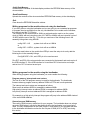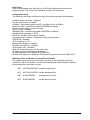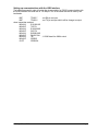
1
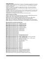
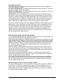
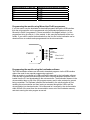
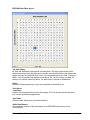
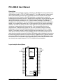
PIC-USB40 User Manual
Description
The module is a single board controller containing an 18F4520 PIC microcontroller and a
USB interface based on FTDI’s FT232R interface IC. The USB interface IC takes care of
all the USB interfacing protocol and is interfaced to the microcontroller via an RS232
transmit and receive connection. No USB knowledge or programming is needed to
interface the microcontroller to the PC which frees up resources in the microcontroller and
eases USB interface development. The module has an onboard type B USB connecter
and 40 pin turned pin connecter on a 0.1” pitch to enable mounting on veroboard or
breadboard for development. The microcontroller is pre-programmed with a bootloader to
enable you to program the module from a USB connection with the supplied bootloader
software. The case may be that you don’t need USB connectivity and just use the USB
connection for programming the microcontroller. The microcontroller can also be
programmed in a standard way without the use of the bootloader using a dedicated
programmer such as Microchips Pickit programmer with connection to pins 1-5 of the
module. The module contains a 10MHz crystal for the microcontroller to run in HS-PLL
mode and run with an instruction cycle of 40MIPS. There is an onboard reset button to
reset the microcontroller at any time with the USB interface also interfacing to the reset so
that the microcontroller can also be reset from the PC application side. Onboard transmit
and receive LED’s provide visual indication of data flow between the USB interface and
the microcontroller. The module can be powered purely from the USB connection or from
an external power supply between 5V to 15V using the onboard regulator.
Layout and pin descriptions
Pin 1
RE3
+V PIC
0V Ground
RB7
RB6
RB5
RB4
RB3
RB2
RB1
RB0
RA5
RA4
RA3
RA2
RA1
RA0
RE2
RE1
RE0
©Kelvyn Shaw 2009
USB
Connector
LED1 LED2
Reset
Switch
+V Reg
0V Ground
+V USB
Sleep
RTS
CTS
RD7
RD6
RD5
RD4
RD3
RD2
RD1
RD0
RC5
RC4
RC3
RC2
RC1
RC0
Page 1
Power Connections
+V Reg. Main regulator input from 5 to 15 volts d.c. The regulator regulates to 5V and has
a dropout voltage of approx 0.3V. The regulator provides a 5V regulated power supply to
the PIC microcontroller.
+V PIC. 5V Output of the regulator to supply external circuitry. This is also Vdd power
supply to the PIC microcontroller. If an external power supply is feed into this pin then it
must not be more than 5.5V
+V USB. 5V output from the USB connection. The 5V is taken from the PC and care must
be taken for how much current is drawn from this pin. If the module is not connected to a
USB port then this connection will be volt free.
0V Ground. Ground/negative/common connection to the whole circuit.
USB Connections and LED’s
Sleep. An output from the USB interface that goes low when the USB interface goes into
suspend mode. Can be used to power down external circuitry.
RTS. Request to Send. An RS232 handshake signal output from the USB interface.
CTS. Clear to Send. An RS232 handshake signal input to the USB interface
LED1. Lights red to indicate the USB interface is transmitting data to the microcontroller.
LED2. Lights green to indicate the USB interface is receiving data from the microcontroller.
Microcontroller Connections and main uses
RA0. Digital input/output port A bit 0. Analogue input AN0.
RA1. Digital input/output port A bit 1. Analogue input AN1.
RA2. Digital input/output port A bit 2. Analogue input AN2.
RA3. Digital input/output port A bit 3. Analogue input AN3.
RA4. Digital input/output port A bit 4. Timer0 clock input
RA5. Digital input/output port A bit 5. Analogue input AN4.
RB0. Digital input/output port B bit 0. Interrupt input 0.
RB1. Digital input/output port B bit 1. Interrupt input 1.
RB2. Digital input/output port B bit 2. Interrupt input 2.
RB3. Digital input/output port B bit 3.
RB4. Digital input/output port B bit 4.
RB5. Digital input/output port B bit 5.
RB6. Digital input/output port B bit 6. Programming Clock Input
RB7. Digital input/output port B bit 7. Programming Data Input
RC0. Digital input/output port C bit 0. Timer 1 oscillator output. Timer 1/3 clock input.
RC1. Digital input/output port C bit 1. Timer 2 oscillator input.
RC2. Digital input/output port C bit 2. Capture and compare output 1. PWM output 1.
RC3. Digital input/output port C bit 3. SPI clock. I2C clock.
RC4. Digital input/output port C bit 4. SPI data input. I2C data.
RC5. Digital input/output port C bit 5. SPI data output.
RD0. Digital input/output port D bit 0. PSP bit 0.
RD1. Digital input/output port D bit 1. PSP bit 1.
RD2. Digital input/output port D bit 2. PSP bit 2.
RD3. Digital input/output port D bit 3. PSP bit 3.
RD4. Digital input/output port D bit 4. PSP bit 4.
RD5. Digital input/output port D bit 5. PSP bit 5.
RD6. Digital input/output port D bit 6. PSP bit 6.
RE7. Digital input/output port D bit 7. PSP bit 7.
RE0. Digital input/output port E bit 0. Analogue input AN5. PSP RD.
RE1. Digital input/output port E bit 1. Analogue input AN6. PSP WR.
RE2. Digital input/output port E bit 2. Analogue input AN7. PSP CS.
RE3. Digital input port E bit 3. Reset input. Programming MCLR input.
©Kelvyn Shaw 2009
Page 2
Powering the module
The module can be powered from the USB connection which falls into two categories or
from an external power supply.
Low Power USB powered. The USB bus provides power for the whole circuit. The circuit
must draw less than 100mA from the bus.
High Power USB powered. The USB bus provides power for the whole circuit. The circuit
must draw less than 500mA from the bus.
Self Powered. The circuit is powered from its own power supply and therefore has not
restrictions on the current it draws and also is able to operate without an USB connection.
However the module is powered the USB interface part of the circuit based around IC2 is
always powered from the USB port. This makes sense as the circuit doesn’t ever need to
be powered unless it is connected to a USB connection. This part of the circuit draws
approx 15mA from the USB hub when running and 70uA when in suspend mode.
If your circuit needs to operate when not connected to USB then it has no option but to be
self powered. If your circuit draws more than 500mA then it must be self powered. If your
circuit draws less than 100mA then it can be powered from the any USB connection. If
your circuit draws less than 500mA but more than 100mA then it can be powered from
USB as long as it is not connected to a hub that isn’t self powered and therefore not
capable of providing 500mA. Also your circuit must not draw more than 100mA until the
host has configured the USB connection.
External power supply and onboard regulator
The onboard regulator regulates the voltage to microcontroller to 5V. A mosfet switch also
provides switching between the USB and external power.
When powering the module from USB then without an external power supply then the USB
voltage supply from the USB bus (+V USB) will be connected to the microcontroller power
supply (+V PIC). When the USB interface is put into USB suspend mode then the mosfet
will switch off power to the microcontroller. Any external circuitry can take power from +V
PIC and will be then be disabled when in USB suspend mode. The mosfet switch can
provide a maximum current of 2A.
When the module is self powered then an external supply is feed into +V REG and the
mosfet switch will switch off to stop +V USB being connected to +V PIC. There will be no
effect on the power to the microcontroller (+V PIC) when in USB suspend mode when be
powered from an external power supply.
If the module is self powered and then connected to a USB bus then the module will
remain being self powered unless the power supply is removed and then the module will
switch to being powered from the USB bus.
If the module is being powered from the USB bus and an external supply is added then
this will have no effect and the module will continue to take its power from the USB bus
until the USB connection is removed and the module will switch to being self powered
from the external power supply.
Maximum regulator current at various supply voltages.
The output of the regulator (+V PIC) is set to 5V. Then input to the regulator (+V REG) can
be from 5V to 15V. There is a voltage drop of approx 0.3V by the regulator so if a 5V
power supply is used then the regulator output will be approx 4.7V which is still fine for
powering the microcontroller. The table below shows the maximum current the regulator
can handle at various supply voltages.
©Kelvyn Shaw 2009
Page 3
Supply Voltage to +V REG pin
15V
12V
9V
8V
6V
5V
Maximum Current through regulator
0.13A
0.18A
0.32A
0.42A
0.65A
1.0A
Programming the module using Microchips PicKit programmer
If you dot want to use the bootloader to download programs through the USB interface
then the microcontroller can be programmed using a standard programmer such as
Microchip’s PicKit 2 programmer. Connect as shown in the diagram with pin 1 of the
programmer lining up with pin 1 of the module. In this case the bootloader will be over
written. If you want to restore the bootloader then the Hex file for the bootloader can be
download from our website and reprogrammed into the microcontroller.
PicKit 2
RE3
+V PIC
0V Ground
RB7
Pins 1-6 of
RB6
RB5
the module
Programming the module using the bootloader software
The USB bootloader software can be used to download programs via the USB interface
without the need for any special programming equipment.
When a module is connected to a USB port it will be detected by the bootloader software.
A hex file that is created from Microchip’s MPLAB or other development software can be
loaded from the PC and downloaded to the microcontroller. The bootloader firmware in the
microcontroller takes up 2K of the 32K program memory and is write protected to prevent
being overwritten. The Software initializes the bootloader in the microcontroller by first
resetting the microcontroller and then issuing a command thought the USB to put the
microcontroller into download mode. If this command isn’t received by the microcontroller
within 300mS of the reset then the microcontroller comes out of the bootloader memory
and starts running the main program as normal.
©Kelvyn Shaw 2009
Page 4
Main Screen Layout.
Target Device.
Displays the name and serial number of the device connected to the USB port. Only one
device can be connected at any one time.
Filename.
Displays the path and filename of the hex file which will be downloaded to the
microcontroller.
Status.
Indicates if the programming or verify was completed successfully or not.
Tools Menu:
-Load File.
Select a hex file from the PC to be programmed.
-Write Program Memory.
Downloads the currently selected Hex file to the microcontroller. Each time you write
program memory the hex file will be reloaded in case it has been updated.
-Verify Program Memory.
Verifies that the selected hex file matches the program memory of the microcontroller.
-Reset Device.
Resets the microcontroller by momentarily pulling down the MCLR pin.
-Edit EEPROM Memory.
Loads the EEPROM editor screen.
©Kelvyn Shaw 2009
Page 5
EEPROM Data Editor layout
The data display.
All Data and addresses are displayed in hexadecimal. The least significant bits of the
address are shown along the top columns and the most significant bits of the address are
shown along the left hand side of the rows. In the screenshot above the LSB = 5 and the
MSB = A so the hexadecimal address of the data is ‘A5’. Double clicking on a data cell
allows you to edit the memory location. The data must be entered in hexadecimal.
Status.
Indicates if the programming or verify was completed successfully or not.
Tools Menu:
-Load Data.
Loads a comma delimited file into the data display. CSV can be imported and exported
from various spreadsheet applications.
-Save Data.
Saves the data display as a comma delimited file.
-Write Data Memory.
Downloads the contents of the data display to the EEPROM Data memory of the
microcontroller.
©Kelvyn Shaw 2009
Page 6
-Verify Data Memory.
Verifies that the contents of the data display matches the EEPROM data memory of the
microcontroller.
-Read Data Memory.
Uploads the contents of the microcontrollers EEPROM Data memory to the data display.
-Exit.
Close down the EEPROM Data editor window.
Writing programs for the module when not using the bootloader
If you don’t plan on using the bootloader and you are going to use a standard programmer
to program the microcontroller then the only considerations to be made are the oscillator,
the reset pin and the TX, RX pins.
The oscillator for the module uses a 10MHz crystal and can be used to run the system
clock at 10MHz with an instruction cycle of 2.5 MIPS or 40MHz with an instruction cycle of
10 MIPS with the use of the PLL. To do this you need one of the following lines in the
assembly listing when using MPLAB.
config OSC = HS
;system clock will run at 10MHz
or
config OSC = HSPLL ;system clock will run at 40MHz
To use the reset button on the module then RE3 pin must the setup to do so by add the
following line in the assembly listings.
Config MCLRE = ON ;set’s RE3 pin to be used as reset
Pins RC7 and RC6 of the microcontroller are connected to the transmit and receive pins of
the USB interface IC. If the USB interface isn’t used then RC6 is best set to and output
and set low. RC7 is best set as an input.
Writing programs for the module using the bootloader
When writing programs using the bootloader you must consider the following.
Program memory, interupt and reset vectors
The first 2K of the 32K program memory is used for the bootloader. The bootloader
firmware takes up program memory address 0000h to 07FFh and is write protected.
The interrupt and reset vectors are remapped as follows.
Reset vector at address 0000h is remapped to address 0800h
High priority interrupt vector at address 0008h is remapped to address 0808h
Low priority interrupt vector at address 0018h is remapped to address 0818h
For example on a high priority interrupt the program will jump to the address 0808h instead
of the usual 0008h address.
General purpose RAM memory
There are no RAM memory restrictions for your program. The bootloader does use a large
amount of RAM when in use but is then freed up when the bootloader is no longer being
used. The only consideration for the RAM is that if a reset arises in your program then due
to the bootloader initialization routine the first 3 bytes of RAM (H’00’ to H’02’) lost during
this routine.
©Kelvyn Shaw 2009
Page 7
Reset Delay
When a reset happens then there will be a 275mS delay between the reset and you
program starting. This is due to an initialization routine of the bootloader.
Configuration Setup
The following is the default configuration setup for the microcontroller with bootloader.
Oscillator switch over mode = Disabled
Fail safe clock monitor = Enabled
Oscillator = High speed oscillator with PLL (oscillator will run at 40MHz)
Brown-out reset = controlled by software (SBOREN bit enabled)
Brown-out reset voltage = minimum setting
Power up timer = Enabled
Watchdog timer = controlled by software (SWDTEN bit enabled)
Watchdog timer postscaler = 32768
MCLR pin = Enabled, RE3 input pin disabled
Low power timer1 oscillator = configured for high power operation
PORTB A/D = Disabled
CCP2 multiplexed = RC1
Background Debugger = Disabled
Extended instruction set = Disabled
Single supply ICSP = Disabled
Stack full or underflow reset = will not cause reset
All code protection is disabled to all addresses
All table read protection is disabled to all addresses
All table write protection is disabled to all addresses except the boot block 0000h-07FFh
Watchdog Timer And Brown-out Control From Software
The watchdog timer and brown-out functions are setup in the configuration bits to be
controlled by the user’s software. Use the following assembly code to enable and disable
the watchdog timer and brown-out reset.
BSF
WDTCON,SWDTEN ;enable watchdog timer
BCF
WDTCON,SWDTEN ;disable watchdog timer
BSF
RCON,SBOREN
;enable brown-out reset
BCF
RCON,SBOREN
;disable brown-out reset
©Kelvyn Shaw 2009
Page 8
Setting up communications with the USB Interface
The following assembly code will setup the microcontroller for RS232 communication with
the USB interface at a baud rate of 115.2Kbps. This is the same rate that is used by the
bootloader.
BSF
TRISC,7
BSF
TRISC,6
when transmitter enabled
MOVLW
B'10100100'
MOVWF
TXSTA
MOVLW
B'10010000'
MOVWF
RCSTA
MOVLW
B'00001000'
MOVWF
BAUDCON
MOVLW
.86
MOVWF
SPBRG
CLRF
SPBRGH
©Kelvyn Shaw 2009
;set RX pin as input
;set TX pin as input which will be change to output
;115200 baud for 40MHz clock
Page 9