1
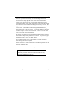
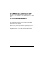
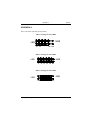
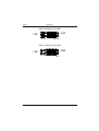
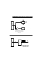
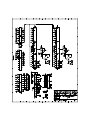
AOP-8
8 Channel Analogue
Output Board
User Manual
AOP-8
User Manual
Document Part N°
Document Reference
Document Issue Level
0127-1011
0127-1011.Doc
1.0
Manual covers PCBs identified
AOP-8 Rev. B
All rights reserved. No part of this publication may be reproduced, stored in any retrieval system, or
transmitted, in any form or by any means, electronic, mechanical, photocopied, recorded or otherwise,
without the prior permission, in writing, from the publisher. For permission in the UK contact Blue Chip
Technology.
Information offered in this manual is correct at the time of printing. Blue Chip Technology accepts no
responsibility for any inaccuracies. This information is subject to change without notice.
All trademarks and registered names acknowledged.
Blue Chip Technology Ltd.,
Chowley Oak, Tattenhall
Chester, Cheshire
CH3 9EX.
Telephone : 01829 772000 Facsimile : 01829 772001.
Amendment History
Issue
Level
0.1
1.0
Issue
Date
08.05.89
12.09.97
Author
JSD
SEJ
Amendment Details
First draft
Update window front cover and logo. See
ECN 98/084
Contents
OUTLINE DESCRIPTION .................................................................. 1
1.0 SPECIFICATIONS ....................................................................... 2
1.1 Electrical Specification ............................................................. 2
1.2 Physical Specification .............................................................. 2
Electromagnetic Compatibility (EMC)............................................. 2
2.0 USER ADJUSTMENTS ................................................................ 5
2.1 Selecting the Base Address...................................................... 5
2.2 Port Map .................................................................................. 6
3.0 ELECTRICAL OPTIONS .............................................................. 8
3.1 Output Connections.................................................................. 8
3.2 Connector Pin Details............................................................... 9
4.0 OPERATING GUIDE.................................................................. 10
4.1 Using the Device.................................................................... 10
4.2 Programming Guide ............................................................... 10
4.3 User Options .......................................................................... 11
5.0 COMMERCIAL DATA ACQUISITION PACKAGES ................... 12
5.1 Use of the AOP-8 Board with ASYST .................................... 12
APPENDIX A ................................................................................... 13
APPENDIX B - PC MAPS................................................................. 15
PC/XT/AT I/O Address Map ......................................................... 15
PC/XT Interrupt Map .................................................................... 16
PC/AT Interrupt Map .................................................................... 17
Blue Chip Technology Ltd.
01271011.doc
Outline Description
Page 1
OUTLINE DESCRIPTION
This card provides 8 analogue outputs in the range 0-10V, at up to 10mA per
channel.
Blue Chip Technology Ltd.
01271011.doc
Page 1
Page 2
Specifications
1.0
SPECIFICATIONS
1.1
Electrical Specification
Number of Outputs
Max Output Voltage
Max Load Current
1.2
8
10.24V D.C.
10mA D.C.
Physical Specification
Height
Width
Depth
107mm
15mm
132mm
Electromagnetic Compatibility (EMC)
This product meets the requirements of the European EMC Directive
(89/336/EEC) and is eligible to bear the CE mark.
It has been assessed operating in a Blue Chip Technology Icon industrial PC.
However, because the board can be installed in a variety of computers, certain
conditions have to be applied to ensure that the compatibility is maintained. It
meets the requirements for an industrial environment (Class A product) subject
to those conditions.
• The board must be installed in a computer system which provides screening
suitable for the industrial environment.
• Any recommendations made by the computer system manufacturer/supplier
must be complied with regarding earthing and the installation of boards.
• The board must be installed with the backplate securely screwed to the
chassis of the computer to ensure good metal-to-metal (i.e. earth) contact.
Page 2
01271011.doc
Blue Chip Technology Ltd.
Specifications
Page 3
• Most EMC problems are caused by the external cabling to the board.
Analogue boards fitted with IDC ribbon cable connectors on the metal
mounting bracket require particularly careful installation of the external
cabling. It is imperative that any external cabling to the board is totally
screened, and that the screen of the cable connects to the metal end bracket
of the board and hence to earth. The cabling must be totally screened; the
type of ribbon cable which is rolled to a round form with a braided wire
screen is best. Standard ribbon cable will not be adequate unless it is
contained wholly within the cabinetry housing the industrial PC. Keep the
unscreened section as short as possible. The mounting bracket of the board
includes a captive nut as an screen earth point. Connect the screen of the
cable to this by the shortest possible wire.
• If difficulty with interference is experienced the cable should also be fitted
with a ferrite clamp as close possible to the connector. The preferred type is
the Chomerics clip-on style, type H8FE-1004-AS.
• It is recommended that cables are kept as short as possible, particularly
when dealing with low level signals.
• Ensure that the screen of the external cable is bonded to a good RF earth at
the remote end of the cable.
Failure to observe these recommendations may invalidate the EMC compliance.
Warning
This is a Class A product. In a domestic environment this
product may cause radio interference in which case the user may
be required to take adequate measures.
Blue Chip Technology Ltd.
01271011.doc
Page 3
Page 4
Specifications
EMC Specification
A Blue Chip Technology Icon industrial PC fitted with this card meets the
following specification:
Emissions
EN 55022:1995
Radiated
Class A
Conducted
Class A & B
Immunity
EN 50082-1:1992 incorporating:
Electrostatic Discharge
IEC 801-2:1984
Performance Criteria B
Radio Frequency Susceptibility IEC 801-3:1984
Performance Criteria A
Fast Burst Transients
IEC 801-4:1988
Performance Criteria B
Page 4
01271011.doc
Blue Chip Technology Ltd.
User Adjustments
2.0
USER ADJUSTMENTS
2.1
Selecting the Base Address
Page 5
The board may be located in any 62 pin slot in the PC motherboard but must be
set up to appear at a specified position (or ‘address’) in the port map. Available
positions are shown in the IBM-PC Technical Reference Guide. However, for
those who do not possess a copy of this document a good place is the location
normally allocated to the prototyping card as supplied by IBM. This address is
300 Hex or 768 decimal.
All Blue Chip Technology cards are preset to this address at the factory.
However, no two devices should be used while set to the same address since
contention will occur and neither board will work. If your machine contains a
card with conflicting address then another reasonably safe address is 200 to 21F
(Hex).
A set of links is provided on the board to set the base address of the board
within the IBM-PC port map. The address is in binary with the presence of a
link representing a 0 and the absence of a link representing a 1.
To set the base address to 768 Decimal (300 Hex) set the following pattern on
the links as indicated:
Blue Chip Technology Ltd.
01271011.doc
Page 5
Page 6
User Adjustments
Figure 1 - Selecting the Base Address
Note: View board with back panel on RHS.
Middle 6 Bits of port address on links.
MSB
LSB
10
20
40
80 100 200
More example addresses are shown in Appendix A.
Note: No two cards must occupy the same address.
2.2
Port Map
The AOP card has up to eight 12 bit analogue output channels. These are
arranged as up to eight pairs of 8 bit ports. One port holds the 8 low bits and
the other the 4 high bits of the desired 12 bit output value. This is shown
below:
Address
Base + 0
Base + 1
Base + 2
Base + 3
Base + 4
Base + 5
Base + 6
Base + 7
Base + 8
Base + 9
Base + 10
Base + 11
Base + 12
Base + 13
Base + 14
Base + 15
Page 6
Write
Channel 0 low 8 bits
Channel 0 high 4 bits
Channel 1 low 8 bits
Channel 1 high 4 bits
Channel 2 low 8 bits
Channel 2 high 4 bits
Channel 3 low 8 bits
Channel 3 high 4 bits
Channel 4 low 8 bits
Channel 4 high 4 bits
Channel 5 low 8 bits
Channel 5 high bits
Channel 6 low bits
Channel 6 high bits
Channel 7 low bits
Channel 7 high 4 bits
01271011.doc
Read
N/A
N/A
N/A
N/A
N/A
N/A
N/A
N/A
N/A
N/A
N/A
N/A
N/A
N/A
N/A
UPDATE
Blue Chip Technology Ltd.
User Adjustments
Page 7
For AOP-2, AOP-4 and AOP-6 all channels begin at 0 e.g. AOP-2 uses Base
+ 0 to Base + 3 other channels are unpopulated.
7
6
5
4
3
2
1
0
ADDRESS XX0H (W/O)
CHANNELS 0 DATA
(BITS 7-0)
7
6
5
4
3
2
1
0
ADDRESS XX1H (W/O)
CHANNELS 0 DATA
(BITS 11-8)
Blue Chip Technology Ltd.
01271011.doc
Page 7
Page 8
Electrical Options
3.0
ELECTRICAL OPTIONS
3.1
Output Connections
A 50 way insulation displacement connector (IDC) is provided on the PC rear
panel of the board for output signal connection. If access to individual channels
is required, a 50 way IDC ribbon cable may be used to connect the outputs to a
50 way screw terminal block available from Blue Chip Technology as part
number ST-24.
The functions of the pins are shown in Section 3.2.
When the connector is viewed from the back of the system, odd numbered pins
are on the left and even numbered pins are on the right with pin 1 at the top of
the connector.
Pin Detail
Pin
Pin
Ο
.
.
.
.
.
.
Pin
Pin
1
3
47
49
Ο
Ο
Ο
Ο
Ο
Ο
Ο
Ο
Ο
Ο
Ο
Ο
Ο
Ο
Ο
Ο
Pin
Pin
.
.
.
.
.
.
.
Pin
Pin
2
4
48
50
View with gold edge connectors downwards.
Page 8
01271011.doc
Blue Chip Technology Ltd.
Electrical Options
3.2
Page 9
Connector Pin Details
Function
Channel 0 + ve
Channel 1 + ve
Channel 2 + ve
Channel 3 + ve
Channel 4 + ve
Channel 5 + ve
Channel 6 + ve
Channel 7 + ve
Analogue Ground
Analogue Ground
Analogue Ground
Analogue Ground
Analogue Ground
Analogue Ground
Analogue Ground
Analogue Ground
Analogue Ground
Analogue Ground
Analogue Ground
Analogue Ground
Analogue Ground
Analogue Ground
Analogue Ground
Analogue Ground
0V
Blue Chip Technology Ltd.
Pin
1 o
3 o
5 o
7 o
9 o
11 o
13 o
15 o
17 o
19 o
21 o
23 o
25 o
27 o
29 o
31 o
33 o
35 o
37 o
39 o
41 o
43 o
45 o
47 o
49 o
Pin
o 2
o 4
o 6
o 8
o 10
o 12
o 14
o 16
o 18
o 20
o 22
o 24
o 26
o 28
o 30
o 32
o 34
o 36
o 38
o 40
o 42
o 44 6
o 46
o 48
o 50
01271011.doc
Function
Analogue Ground
Analogue Ground
Analogue Ground
Analogue Ground
Analogue Ground
Analogue Ground
Analogue Ground
Analogue Ground
Analogue Ground
Analogue Ground
Analogue Ground
Analogue Ground
Analogue Ground
Analogue Ground
Analogue Ground
Analogue Ground
Analogue Ground
Analogue Ground
Analogue Ground
Analogue Ground
Analogue Ground
Analogue Ground
Analogue Ground
Analogue Ground
0V
Page 9
Page 10
Operating Guide
4.0
OPERATING GUIDE
4.1
Using the Device
The normal method of setting an output is:
1.
2.
3.
Load data by writing to low byte port.
Load data on writing to high NIBL port.
Strobe data to output by reading UPDATE port.
The digital to analogue converters used on this board contain a buffer and the
data is initially written into this buffer without changing the output voltage.
The output voltages are not altered until the UPDATE command is performed
which transfers the data from all buffers to their respective output register
without altering the data in the buffers. Thus single channels may be updated
using an UPDATE command immediately after loading data for one channel, or
several output signals may be changed simultaneously by first loading data into
the relevant buffers and then issuing the UPDATE command.
The procedure for a single output is illustrated in the software example.
4.2
Programming Guide
The output signals may be set as shown in the following example using
Microsoft BASIC A or GW BASIC:
10
20
30
40
50
60
70
INPUT
BITS
TOP
BOT
OUT
OUT
A
″Enter voltage required″:V
= V*400
= INT(BITS/256)
= INT (BITS-256xTOP)
&H300,BOT
&H301, TOP
= INP (&H30F)
′Set bottom byte
′Set top NIBL
This example assumes a standard board set for 2.5mV/bit or 0-10.24V output
and sets only channel 0 as controlled by the ′OUT′ statements in lines
50 and 60.
Page 10
01271011.doc
Blue Chip Technology Ltd.
Operating Guide
4.3
Page 11
User Options
a. Grounding
The analogue ground for the outputs can be linked to digital ground
using a link option (LKB). When the link is fitted the two grounds are
connected. Conversely with the link removed the grounds are allowed
to float at different voltages up to +/- 0.6V under the clamping action
of diodes D2 and D3.
b. Calibration
A 10V reference is generated for all channels from diode D1 and IC5.
This voltage may be trimmed using RV5 or completely re-scaled by
changing R1, R2 or D1. Individual channels can be trimmed by
trimpots as follows:
Channel
0
1
2
3
4
5
6
7
Blue Chip Technology Ltd.
Trimpot Ref.
RV2
RV1
RV7
RV6
RV4
RV3
RV9
RV8
01271011.doc
Page 11
Page 12
Commercial Data Acquisition Packages
5.0 COMMERCIAL DATA ACQUISITION PACKAGES
The Blue Chip Technology DOP-24 can be used with almost any data
acquisition or control package that can write information directly to a PC output
port.
5.1 Use of the AOP-8 Board with ASYST
The board has been tested with and is installable as an IO.PORT digital device
in the ASYST scientific software package by Macmillan Software Company.
For more details about this package and other PC data acquisition software,
please contact Blue Chip Technology.
Whilst every effort has been taken to ensure that the information provided is
accurate, Blue Chip Technology cannot assume responsibility for any errors in
this manual or their consequences. Should any errors be detected, the company
would greatly appreciate being informed of them. A policy of continuos product
development is operated, resulting in the contents of this document being
subject to change without notice.
Page 12
01271011.doc
Blue Chip Technology Ltd.
Appendix A
Page 13
APPENDIX A
Note view board with back panel on RHS.
Address Settings for Port 300H
MSB
LSB
10
40
20
80 100 200
Address Settings for Port 200H
MSB
LSB
10
20
40
80 100 200
Address Settings for Port 210H
MSB
LSB
10
Blue Chip Technology Ltd.
20
40
80 100 200
01271011.doc
Page 13
Page 14
Appendix A
Address Settings for Port 220H
MSB
LSB
10
20
40
80 100 200
Address Settings for Port 230H
MSB
LSB
10
Page 14
20
40
80 100 200
01271011.doc
Blue Chip Technology Ltd.
Appendix B
Page 15
APPENDIX B - PC MAPS
PC/XT/AT I/O Address Map
Address
Allocated to:
000-01F
020-03F
040-05F
060-06F
070-07F
080-09F
0A0-0BF
0F0
0F1
0F8-0FF
1F0-1F8
200-207
278-27F
2F8-2FF
300-31F
360-36F
378-37F
380-38F
3A0-3AF
3B0-3BF
3C0-3CF
3D0-3DF
3F0-3F7
3F8-3FF
DMA Controller 1 (8237A-5)
Interrupt Controller 1 (8259A)
Timer (8254)
Keyboard Controller (8742) Control Port B
RTC and CMOS RAM, NMI Mask (Write)
DMA Page Register (Memory Mapper)
Interrupt Controller 2 (8259)
Clear NPX (80287) Busy
Reset NPX (80287)
Numeric Processor Extension (80287)
Hard Disk Drive Controller
Reserved
Reserved for Parallel Printer Port 2
Reserved for Serial Port 2
Reserved
Reserved
Parallel Printer Port 1
Reserved for SDLC Communications, Bisync 2
Reserved for Bisync 1
Reserved
Reserved
Display Controller
Diskette Drive Controller
Serial Port 1
Blue Chip Technology Ltd.
01271011.doc
Page 15
Page 16
Appendix B
PC/XT Interrupt Map
Number
Allocated to:
NMI
0
1
2
3
Parity
Timer
Keyboard
Reserved
Asynchronous Communications (Secondary)
SDLC Communications
Asynchronous Communications (Primary)
SDLC Communications
Fixed Disk
Diskette
Parallel Printer
4
5
6
7
Page 16
01271011.doc
Blue Chip Technology Ltd.
Appendix B
Page 17
PC/AT Interrupt Map
Level
Allocated to:
CPU NMI
CTLR 1
Parity or I/O Channel Check
CTLR 2
IRQ 0
IRQ 1
IRQ 2
IRQ 8
IRQ 9
IRQ 10
IRQ 11
IRQ 12
IRQ 13
IRQ 14
IRQ 15
IRQ 3
IRQ 4
IRQ 5
IRQ 6
IRQ 7
Blue Chip Technology Ltd.
(Interrupt Controllers)
Timer Output 0
Keyboard (Output Buffer Full)
Interrupt from CTLR 2
Real-time Clock Interrupt
S/w Redirected to INT 0AH (IRQ 2)
Reserved
Reserved
Reserved
Co-processor
Fixed Disk Controller
Reserved
Serial Port 2
Serial Port 1
Parallel Port 2
Diskette Controller
Parallel Port 1
01271011.doc
Page 17
Typical Methods of Interfacing from an AOP card to other Circuitry
5V
OUT
LM35
TEMP'
SENSOR
AOP
P1/1
0V
HEATER
The Analogue Output card can be used as a
voltage reference in a closed loop temperature
monitoring circuit
AOP
FCLK
P1/1
Vin
Voltage
to
frequency
The Analogue Output can be fed into
a voltage to frequency converter