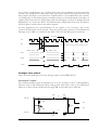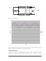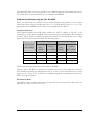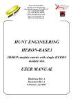
1
HUNT ENGINEERING
Chestnut Court, Burton Row,
Brent Knoll, Somerset, TA9 4BP, UK
Tel: (+44) (0)1278 760188,
Fax: (+44) (0)1278 760199,
Email: [email protected]
http://www.hunteng.co.uk
http://www.hunt-dsp.com
HUNT ENGINEERING
HERON-IO5
HERON Module with 1.5 or 3M gate FPGA
and 2 channels of 210Mhz 12 bit A/D
and 2 channels of 160Mhz 16 bit D/A
(including differential D/A output option)
USER MANUAL
Hardware Rev B
Document Rev G
T.Hollis 13/07/05
COPYRIGHT
This documentation and the product it is supplied with are Copyright HUNT
ENGINEERING 2004/5. All rights reserved. HUNT ENGINEERING maintains a
policy of continual product development and hence reserves the right to change product
specification without prior warning.
WARRANTIES LIABILITY and INDEMNITIES
HUNT ENGINEERING warrants the hardware to be free from defects in the material
and workmanship for 12 months from the date of purchase. Product returned under the
terms of the warranty must be returned carriage paid to the main offices of HUNT
ENGINEERING situated at BRENT KNOLL Somerset UK, the product will be repaired
or replaced at the discretion of HUNT ENGINEERING.
If HUNT ENGINEERING decides that there is any evidence of
electrical or mechanical abuse to the hardware, then the customer shall have no
recourse to HUNT ENGINEERING or its agents. In such circumstances HUNT
ENGINEERING may at its discretion offer to repair the hardware and charge for
that repair.
Exclusions -
Limitations of Liability - HUNT
ENGINEERING makes no warranty as to the fitness of
the product for any particular purpose. In no event shall HUNT
ENGINEERING’S liability related to the product exceed the purchase fee actually
paid by you for the product. Neither HUNT ENGINEERING nor its suppliers
shall in any event be liable for any indirect, consequential or financial damages
caused by the delivery, use or performance of this product.
Because some states do not allow the exclusion or limitation of incidental or consequential
damages or limitation on how long an implied warranty lasts, the above limitations may not
apply to you.
TECHNICAL SUPPORT
Technical support for HUNT ENGINEERING products should first be obtained from the
comprehensive Support section http://www.hunteng.co.uk/support/index.htm on the
HUNT ENGINEERING web site. This includes FAQs, latest product, software and
documentation updates etc. Or contact your local supplier - if you are unsure of details
please refer to http://www.hunteng.co.uk for the list of current re-sellers.
HUNT ENGINEERING technical support can be contacted by emailing
[email protected], calling the direct support telephone number +44 (0)1278
760775, or by calling the general number +44 (0)1278 760188 and choosing the technical
support option.
2
HUNT ENGINEERING HERON-IO5V USER MANUAL
TABLE OF CONTENTS
INTRODUCTION.......................................................................................................... 6
PHYSICAL LOCATION OF ITEMS ON THE HERON-IO5.................................. 8
GETTING STARTED ................................................................................................... 9
STANDARD INTELLECTUAL PROPERTY (IP) ............................................................................................. 9
MODULE FEATURES ............................................................................................... 10
SERIAL CONFIGURATION OF THE USER FPGA ....................................................................................... 10
BOOT ROM........................................................................................................................................... 10
CLOCKING OF THE FPGA ...................................................................................................................... 11
HERON FIFOS .................................................................................................................................... 12
ANALOG I/O .......................................................................................................................................... 13
A/D clocking .................................................................................................................................... 13
D/A clocking .................................................................................................................................... 14
DIGITAL I/O........................................................................................................................................... 14
MODULE AND CARRIER ID .................................................................................................................... 15
GENERAL PURPOSE LEDS ..................................................................................................................... 15
DONE LEDS .......................................................................................................................................... 15
GETTING STARTED ON YOUR FPGA DESIGN ................................................. 16
WORKING THROUGH EXAMPLE 1........................................................................................................... 17
Preparing ISE .................................................................................................................................. 17
Copying the examples from the HUNT ENGINEERING CD........................................................... 18
Opening the Example1 Project........................................................................................................ 18
The Project's functional parameters................................................................................................ 18
Setting up the Configuration Package............................................................................................. 19
User Timing Constraints.................................................................................................................. 22
Creating the Bitstream for Example1 .............................................................................................. 24
Simulating the complete design ....................................................................................................... 25
MAKING YOUR OWN FPGA DESIGN................................................................... 26
USER_AP INTERFACE ............................................................................................................................ 26
HARDWARE INTERFACE LAYER ............................................................................................................. 31
IMPORTANT!.......................................................................................................................................... 33
OTHER EXAMPLES ................................................................................................................................. 33
HOW TO MAKE A NEW DESIGN ............................................................................................................. 34
Inserting your own Logic................................................................................................................. 34
Top-level fine tuning (using other special IO pins) ......................................................................... 34
User Timing Constraints.................................................................................................................. 35
HINTS FOR FPGA DESIGNS .................................................................................................................... 35
Use of Clocks ................................................................................................................................... 36
Possible Sources of Clocks .............................................................................................................. 36
Flow Control.................................................................................................................................... 37
Pipeline Length or “latency” .......................................................................................................... 37
DIGITAL I/O FROM THE FPGA............................................................................................................... 37
DSP WITH YOUR FPGA......................................................................................................................... 38
CHIPSCOPE ............................................................................................................................................ 38
SOFTWARE................................................................................................................. 40
FPGA DEVELOPMENT TOOL.................................................................................................................. 40
DESIGN FILES FOR THE FPGA ............................................................................................................... 40
GENERATING DESIGN FILES................................................................................................................... 41
Files for HERON Utility (*.RBT)..................................................................................................... 41
Files for direct JTAG programming (*.bit) ..................................................................................... 42
3
HUNT ENGINEERING HERON-IO5V USER MANUAL
Files for PROMs (*.MCS) ............................................................................................................... 42
DOWNLOADING FILES VIA JTAG........................................................................................................... 42
HERON_FPGA CONFIGURATION TOOL ............................................................................................... 43
HUNT ENGINEERING HOST-API.................................................................................................... 43
HUNT ENGINEERING HERON-API................................................................................................. 43
HARDWARE DETAILS ............................................................................................. 44
HERON MODULE TYPE ........................................................................................................................ 44
HARDWARE RESET ................................................................................................................................ 44
SOFTWARE RESET (VIA SERIAL BUS) ..................................................................................................... 44
CONFIG.................................................................................................................................................. 45
DEFAULT ROUTING JUMPERS ................................................................................................................ 45
PHYSICAL DIMENSIONS OF THE MODULE .............................................................................................. 45
POWER REQUIREMENTS OF THE HERON-IO5....................................................................................... 46
FPGA POWER CONSUMPTION/DISSIPATION ........................................................................................... 46
FIFOS ................................................................................................................................................... 48
USER FPGA CLOCKING......................................................................................................................... 50
User oscillators................................................................................................................................ 51
AC CLOCK Connector type............................................................................................................. 51
ESD protection ................................................................................................................................ 51
ANALOG I/O .......................................................................................................................................... 52
Analog input connector type HERON-IO5 ...................................................................................... 52
Analog input connector type HERON-IO5-DO ............................................................................... 53
ADC data ......................................................................................................................................... 54
ADC missing codes .......................................................................................................................... 57
ADC clocking................................................................................................................................... 57
ADC pipeline delay.......................................................................................................................... 59
ADC Output synchronisation........................................................................................................... 59
Analogue input options.................................................................................................................... 60
ESD protection ................................................................................................................................ 64
Differential inputs............................................................................................................................ 64
Cabling precautions ........................................................................................................................ 69
Analogue output connector type ...................................................................................................... 70
AD9777 DUAL DIGITAL TO ANALOGUE CONVERTER ........................................................................... 70
DAC Data ....................................................................................................................................... 71
DAC Clocking.................................................................................................................................. 71
DAC Latency.................................................................................................................................... 72
Serial Port Interface ........................................................................................................................ 72
DAC Configuration Options ............................................................................................................ 72
Problem found when using the PLL Enabled .................................................................................. 73
D/A Output Noise............................................................................................................................. 75
Analogue output options.................................................................................................................. 75
HERON-IO5-DO DAC OUTPUTS .................................................................................................. 76
Short Circuit protection................................................................................................................... 77
ESD protection ................................................................................................................................ 77
Cabling precautions ........................................................................................................................ 78
DIGITAL I/O........................................................................................................................................... 78
I/O characteristics ........................................................................................................................... 78
Using Digitally Controlled Impedance (DCI) ................................................................................. 78
“DIGITAL I/O” Connector type...................................................................................................... 79
“DIGITAL I/O” Connector Pin out................................................................................................. 79
ESD protection ................................................................................................................................ 79
THE JTAG PROGRAMMABLE CONFIGURATION PROM.......................................................................... 80
USER FPGA BOOT FROM PROM JUMPER............................................................................................. 80
UNCOMMITTED MODULE INTERCONNECTS ........................................................................................... 81
GENERAL PURPOSE LEDS ..................................................................................................................... 81
OTHER HERON MODULE SIGNALS ........................................................................................................ 81
4
HUNT ENGINEERING HERON-IO5V USER MANUAL
FITTING MODULES TO YOUR CARRIER .......................................................... 82
ACHIEVABLE SYSTEM THROUGHPUT ............................................................. 83
TROUBLESHOOTING .............................................................................................. 84
HARDWARE ........................................................................................................................................... 84
SOFTWARE ............................................................................................................................................ 84
CE MARKING ............................................................................................................. 85
TECHNICAL SUPPORT............................................................................................ 86
APPENDIX 1 – HERON SERIAL BUS COMMANDS ........................................... 87
MODULE ADDRESS ................................................................................................................................ 87
MODULE ENQUIRY ................................................................................................................................ 87
FPGA CONFIGURATION ........................................................................................................................ 87
USER I/O ............................................................................................................................................... 88
APPENDIX 2 – FPGA PINOUT FOR DEVELOPMENT TOOLS ........................ 89
5
HUNT ENGINEERING HERON-IO5V USER MANUAL
Introduction
The HERON module is a module defined by HUNT ENGINEERING to address the
needs of our customers for real-time DSP systems. The HERON module is defined both
mechanically and electrically by a separate HERON module specification that is available
from the HUNT ENGINEERING CD, via the user manual section from the CD browser,
or online from http://www.hunteng.co.uk and going to the application note section under
the user area.
The HERON module specification also defines the features that a HERON module carrier
must provide. HERON stands for Hunt Engineering ResOurce Node, which tries to make
it clear that the module is not for a particular processor, or I/O task, but is intended to be a
module definition that allows “nodes” in a system to be interconnected and controlled
whatever their function. In this respect it is not like the TIM-40 specification which was
specific to the ‘C4x DSP.
As the HERON-IO5 was developed, HUNT ENGINEERING have already developed
HERON modules carriers like the HEPC9, HERON processor modules (that carry various
other members of the TMS320C6000 family of DSP processors from TI), and are working
on new HERON-IO modules. In addition to these modules, the HERON specification is a
super-set of the pre-existing HUNT ENGINEERING GDIO module, so the GDIO
modules from our C4x product range can also be used in HERON systems.
The HERON module connects to the carrier board through several standard interfaces.
•
The first is a FIFO input interface, and a FIFO output interface. This is to be used for
the main inter-node communications. (It is usually also used for connection to the
HOST computer if any).
•
The second is an asynchronous interface that allows registers etc to be configured from
a HERON module. This is intended for configuring communication systems, or
perhaps to control some function specific peripherals on the carrier board.
•
The third is a JTAG (IEEE 1149.1) interface for running processor debug tools.
•
The Fourth is the HERON Serial Bus, used for configuration messages.
•
The last is the general control such as reset, power etc.
HUNT ENGINEERING defined the HERON modules in conjunction with HEART –
the Hunt Engineering Architecture using Ring Technology. This is a common architecture
that we will adopt for our HERON carriers that provides good real time features such as
low latency and high bandwidth, along with software reconfigurability of the
communication system, multicast, multiple board support etc., etc.
However, it is not a requirement of a HERON module carrier that it implements such
features. In fact our customers could develop their own module carrier and add our
HERON modules to it. Conversely our customers could develop application specific
HERON modules themselves and add them to our systems.
The HERON-IO5 is a HERON module that has 2 channels of 210Mhz 12 bit A/D and 2
channels of 160Mhz 16 bit D/A and some General Purpose Digital I/O. This means the
HERON-IO5 will be used mainly as a flexible Analog I/O module, but one that can
optionally be programmed to perform hardware signal processing on that I/O.
6
HUNT ENGINEERING HERON-IO5V USER MANUAL
The HERON-IO5 provides a 1.5M or 3M gate FPGA from the Xilinx Virtex II family.
This is a high performance part that has specific optimisations for Digital Signal Processing
that can be loaded with bit-streams provided by HUNT ENGINEERING or developed by
the user.
The HERON-IO5 connects all of the HERON module signals, except the JTAG, to the
FPGA, allowing flexible use of the module’s resources.
The HERON-IO5 connects some of the FPGA I/Os to a digital I/O connector on the
module. This allows the FPGA to be configured for a variety of I/Os.
The HERON-IO5 uses the HERON module’s serial bus to download configuration bit
streams into the FPGA, allowing the user to configure it with standard functions provided
by HUNT ENGINEERING or functions that they have developed themselves using the
Xilinx development tools.
Programmers of the FPGA can also use more comprehensive development packages for
the FPGA such as the ISE from Xilinx. These tools require a license fee to be paid to
Xilinx.
There is also the possibility for the module to configure the FPGA part from a JTAG
programmable FLASH ROM. This is intended to simplify the deployment of systems after
the FPGA functions have been fully developed.
The HERON-IO5-DO is the same as the HERON-IO5 with the exception that the D/A
outputs are differential, and there is a site for a second LVDS User Oscillator capable of
frequencies up to 250MHz. This oscillator is not fitted as standard. The D/A output level
on the HERON-IO5-DO is higher than the IO5, giving a differential output level of 4.2
Volts pk-pk.
7
HUNT ENGINEERING HERON-IO5V USER MANUAL
Physical Location of Items on the HERON-IO5
Analog
3.3V OK
-3.3V
Analog Power Circuits
HERON connector with Default Routing jumpers
HERON connector
Analogue Inputs
Analogue
Outputs
A/Ds
(AD9430)
D/A
AD9777
AC Clock
input
User
FPGA
boot from
prom
Control FPGA
“DONE LED”
User FPGA
Virtex 2 1500Kgate
FPGA
PROM
JTAG
for
PROM
Digital
I/O
1.5V power circuit
3.3V power circuit
3.3V OK
“DONE
HERON connector
1.5V OK
HERON connector
General
Purpose
LEDs
8
HUNT ENGINEERING HERON-IO5V USER MANUAL
Getting Started
The HERON-IO5 is a module that plugs into a HERON module carrier.
The HERON-IO5 should be fitted to the carrier card along with any other modules that
your system has and their retaining nuts fitted (see a later section of this manual for details).
The Default routing jumpers must be set correctly for the system. For most systems the
FPGA based modules will not require any default routing jumpers to be fitted. This will
allow the FPGA to access whatever FIFO it needs to, and will rely on the FIFO being
connected to the right place by the carrier configuration. (See a later section for details on
default routing jumpers).
There is only one user configurable jumper on the HERON-IO5 and that controls the
PROM option.
The HERON-IO5, following reset, will enter a state where it can be interrogated and
programmed using the HERON module’s serial bus. It is addressed according to the
Carrier number and the slot number of the HERON slot that it is fitted to.
The FPGA configuration data will have been generated using the Xilinx development tools.
HUNT ENGINEERING provides examples for the HERON-FPGA modules in the
correct format for use with the Xilinx ISE software. HUNT ENGINEERING also
provides software for the Host PC that will allow the output files from the ISE software to
be loaded onto a HERON-FPGA module.
Follow the “Starting your FPGA development” tutorial from the Getting started section of
the HUNT ENGINEERING CD, and then the examples that are specific to the HERONIO5.
It could be possible to use the HERON-IO5 as an I/O module using one of the example
bit streams. In this case it is not necessary to be concerned how to program the FPGA –
simply load the example bit stream and use it.
Standard Intellectual Property (IP)
HUNT ENGINEERING provides examples for the HERON-IO5 that perform different
functions. It is possible to use these standard configurations directly if they fit your needs.
It could be possible to request a new standard example from HUNT ENGINEERING,
which could avoid the need to purchase and learn how to use the FPGA development
tools. Depending on the complexity of your request HUNT ENGINEERING may choose
not to offer it, or to charge for it.
New IP for the HERON-IO5 will be posted on the HUNT ENGINEERING web site in
the user area whenever it becomes available. HERON-IO5 users can then take advantage
of that IP free of charge.
9
HUNT ENGINEERING HERON-IO5V USER MANUAL
Module Features
This section describes the features of the HERON-IO5 and why they are provided.
8 bits Digital I/O & LEDS
I/P
connectors
O/P
connectors
2 x A/Ds
2x D/As
Power
Supply Cct
JTAG PROM
Clock
options
FPGA
Virtex II 1.5M or 3M gates
Configuration
control FPGA
HERON FIFO CONNECTIONS
HERON CONTROLS
HERON Serial Bus
BLOCK diagram
Serial Configuration of the User FPGA
The HERON-IO5 usually has the configuration of the User FPGA downloaded using the
HERON module’s serial configuration bus. This allows the use of “standard”
configurations as supplied on the HUNT ENGINEERING CD, or of user defined
configurations without the need to return the module to the factory.
It is imagined that as the “standard” set of functions grows, that they be made available to
users of HERON-FPGA and IO modules via the HUNT ENGINEERING web site or
CD update requests. Also HUNT ENGINEERING will have the possibility to provide
semi-custom configurations for a charge via email.
Boot ROM
As an alternative to the serial configuration download, it is possible to configure the FPGA
from a Flash based configuration PROM. It is an advantage when the DSP system will be
ROM booted, as it removes the need for the DSP FLASH ROM to store the configuration
for the FPGA too. However, if a system is being deployed with a host machine such as a
PC, it might be preferable to continue to use the serial configuration method, as this will
make in field upgrades and bug fixes simpler to deploy.
The PROMS fitted to the HERON-IO5 are Flash based, and can be programmed (and reprogrammed) using a Xilinx JTAG cable (such as Xilinx parallel cable 4, or USB cable).
10
HUNT ENGINEERING HERON-IO5V USER MANUAL
Clocking of the FPGA
The Xilinx FPGA used on the HERON-IO5 does not have a single clock input, but rather
it can use any one of its pins to provide a clock input. This means you can have many
sources of clocks, each of which can be used inside your FPGA design. You can even
divide these clocks using flip flops, or even multiply using digital clock manager
components.
Clock Options
Necessary clocks
OSC1 (100Mhz)
Output FIFO clock
OSC2( -DO only)
feedback
8 Bit Digital I/O
Input FIFO clock
Your FPGA design
feedback
UMI0,1,2&3
ADC Clocks
ADC data Clock
AC Clock Input
DAC Clocks
DAC data Clock
The simplest way to manage your FPGA design is to use just one clock throughout your
design. However the FPGA must drive both of the HERON FIFO clocks, at a frequency
that is suitable for your module carrier (see the documentation for your module carrier for
details of its restrictions). The FPGA must also drive the A/D clocks, and the D/A clocks.
The frequency for these might be limited by the components, or by the needs of your signal
processing. The needs for these clocks can only be determined by looking carefully at the
needs of your system.
The ‘AC CLK’ input can be used as a clock source for the FPGA and/or a clock for the
A/D converters. This 50 Ohm input can be driven with a low level sinusoid, or by logic
levels such as LVTTL. The selection of clock signals for the A/D converters is achieved
with a LVPECL multiplexer, this allows the FPGA or the ‘AC CLK’ input to source the
clock for each or both of the A/D converters. If the ‘AC CLK’ input is selected as the
source for both of the converters then the maximum propagation delay through the active
devices is 965 picoSeconds at 25 degC, and the maximum skew is 100 picoSeconds. It is
recommended that if the ‘AC CLK’ input is used to clock the A/D converters a sinusoid is
used to drive the input as this will give the best jitter performance.
On the HERON-IO5-DO there is a site for a second surface mount user crystal oscillator,
an oscillator is not fitted here as standard build. The OSC2 site is for a 3.3Volt LVDS
oscillator, Golledge type GXO-L71 or equivalent, which allows oscillator frequencies up to
250MHz.
The AD9430 A/D converters used on the HERON-IO5 generate a ‘data clock’ that is
synchronised to the data output from that converter to facilitate registering of the data into
the FPGA, this then becomes a clock input to the FPGA for use with associated logic.
The AD9777 D/A converter used on the HERON-IO5 also generates a ‘data clock’. This
is synchronised to when the DAC expects data on its ports in the operating mode where the
PLL is disabled. If the PLL is enabled then the timing of the data clocked into the D/A is
related to the ‘sample clock’ not to the ‘data clock’ generated by the D/A.
The most difficult case for your FPGA design is to have many clocks from different
sources that are all used in the same design. Then you must carefully manage signals that
11
HUNT ENGINEERING HERON-IO5V USER MANUAL
cross from one clock “domain” to another. This can be handled by FIFOS, or by multiple
registering to prevent metastability problems. Refer to texts on digital design to understand
these issues.
Clock Options
OSC1 (100Mhz)
Div2?
8 Bit Digital I/O
UMI0,1,2&3
logic
‘AC CLK’ input
FIFOs
Necessary clocks
Output FIFO clock
feedback
Input FIFO clock
feedback
ADC Clocks
ADC data Clock
DAC Clocks
DAC data Clock
Example3 design
Example3 for the HERON-IO5 uses two separate clock sources, one for the ADCs (‘AC
CLK’ input) and another for the FIFOS and logic (OSC1). This example uses FIFOS to
pass data from one clock domain to the other.
The HERON-IO5 provides a highly flexible set of choices for the clocking of the FPGA,
D/As and A/Ds.
Default shipping state is to have a 100Mhz oscillator fitted to the surface mount sites –
driving 100Mhz on UserOsc1. This is a standard commercial oscillator module, that is +100ppm accuracy with typically 8ps of jitter (max 99ps). If you require higher accuracy for
your analogue clocks then you should use one of the other clock sources.
Any of the digital I/Os on the digital I/O connectors or the UMI pins on the module
connector could be used as a clock input or output.
HERON FIFOS
The HERON module can access up to 6 input FIFOs and up to another 6 output FIFOs.
Actually it is most likely that a carrier board will not implement all 12 FIFO interfaces. Each
FIFO interface is the same as the others, using common clocks and data busses.
The input and output interfaces are separate though, allowing data to be read and written at
the same time by a module like the HERON-IO5.
While it is possible to read one FIFO and write another FIFO at the same time, the use of
shared pins means no more than one can be written or read at the same time.
For each interface (input or output) there is a FIFO clock that must be a constant
frequency, and running constantly. There may be some minimum and maximum frequency
requirements for a particular Module Carrier card that the designer of the FPGA contents
must be sure to comply with. This is because the FIFO clocks are generated by the FPGA,
probably based on one of the clock inputs to the FPGA .
12
HUNT ENGINEERING HERON-IO5V USER MANUAL
Each FIFO interface has a separate “enable” signal that is used to indicate which FIFO is
accessed using the clock edge.
Input FIFOs
The input FIFOs use a common data bus that is driven onto the HERON module. It is
important to ensure that no more than one of the FIFOs are read at the same time, but
more importantly that no more than one has its output enable selected.
By properly asserting the “read enable” and “output enable” signals relative to the clock the
FPGA can access the FIFO of its choice at a rate up to one 32 bit word per clock cycle.
For the timing of those signals refer to the HERON module specification.
Each input FIFO interface provides Flags that indicate the state of the FIFO. An empty
flag shows that there is no data to be read, an almost empty flag shows that there are at least
4 words left. While the almost flag is not asserted accesses can be made on every clock, but
after it is asserted, it is better to make one access only, then check the empty flag on the
next clock, before deciding if another access is possible.
Output FIFOs
The output FIFOs use a common data bus that is driven by the HERON module. It is
important to ensure that no more than one of the FIFOs is written at the same time –
unless that is required by your system.
By properly asserting the “write enable” signals relative to the clock, the FPGA can access
the FIFO of its choice at a rate up to one 32-bit word per clock cycle.
For the timing of those signals refer to the HERON module specification.
Each output FIFO interface provides Flags that indicate the state of the FIFO. A full flag
shows that there is no room left to write, an almost full flag shows that there are at least 4
words of space left. While the almost flag is not asserted accesses can be made on every
clock, but after it is asserted, it is better to make one access only, then check the full flag on
the next clock, before deciding if another access is possible.
FIFO clocks
The FIFO clocks are provided by the FPGA, but are buffered externally using an LVT245
buffer that is able to provide the drive current required on these signals. To enable circuitry
internal to the FPGA to be designed to use the actual clock that is applied to the FIFO, the
buffered FIFO clock signals are connected to some GCLK inputs. This allows DLLs to be
used to provide a clock internal to the FPGA that has the same phase as that applied to the
FIFOs on the carrier board.
Analog I/O
The HERON-IO5 connects the FPGA to two 12 bit A/D chips that can sample at rates
between 40 and 210MHz. This allows the User FPGA program to sample the A/D data,
process it, store it or pass it on to another HERON module as the user’s system requires.
The HERON-IO5 also connects the FPGA to two 16 bit D/A’s that can be clocked at up
to 160MHz.
A/D clocking
The A/D’s on the HERON-IO5 can be clocked either from the FPGA or from the ‘AC
13
HUNT ENGINEERING HERON-IO5V USER MANUAL
CLK’ input. If the FPGA is used as the source then the clock can be derived from the User
oscillator, digital I/O connector, the HERON UMI pins, or even indirectly using the ‘AC
CLK’ input via the FPGA.
The selection between the ‘AC CLK’ input and the FPGA as the source of the A/D clock
signal is achieved with a LVPECL multiplexor controlled by logic levels from the FPGA.
The output data from each of the A/D converters is in the form of two 12bit output busses
together with an output data clock, running at half the sample frequency. This output data
clock is used to register the data into the FPGA.. The management of this is taken care of
in the Hardware Interface Layer VHDL provided.
Each A/D has a separate clock input so they can be driven at different frequencies or
phases, for example one could be driven from the ‘AC CLK’ input while the other is driven
from the FPGA. For applications that require the converters to be clocked by the same
sample clock then the use of the ‘AC CLK’ input is preferable, as the delays within the
FPGA are not incurred. The maximum skew between the two A/D converter clocks
introduced by the active devices on the ‘AC CLK’ input is 100 picoSeconds at 25 degC.
The ‘AC CLK’ input does have a direct link to the FPGA and so can be used as a clock
input to the FPGA. The use of the ‘AC CLK’ input for the A/D’s without going through
the FPGA is preferable as there is no extra delay or additional jitter introduced.
The lower frequency limit of the ‘AC CLK’ input is approximately 4 MHz when driving the
input with a 0 dBm sine wave. The minimum sample frequency for the A/D converters is
40 MHz.
D/A clocking
The D/As are clocked by the FPGA, this clock can be derived from the User Oscillator,
digital I/O connector, HERON UMI pins or the ‘AC CLK’ input.
The FPGA directly drives the sample clock inputs of the D/A converters, with no buffer
delays. The two D/A channels have only one clock input. The D/A converter generates an
output clock to register the D/A data for both channels out of the FPGA, when the
internal PLL is not enabled, the management of this is taken care of in the Hardware
Interface Layer VHDL provided.
The D/A device comes out of reset as a two channel D/A converter, but it can be
programmed over a serial bus, linked to the FPGA, to perform more complex functions.
This is covered in more detail in a later section of this document.
Digital I/O
The HERON-IO5 connects 8 of the FPGA’s I/O pins to connectors. All of the digital I/O
pins are connected to differential pairs of I/O pins on the FPGA so that the digital I/O can
be used for differential as well as single ended digital inputs or outputs as determined by the
user’s FPGA program. In particular two of the digital I/O pins are connected to a GCLK
differential pair of pins on the FPGA, this makes them particularly suitable for an external
clock input.
On the HERON-IO5 all the digital I/O is connected to bank 5 of the FPGA which has its
VCCO fixed at 3.3 Volts so that the formats supported by the Digital I/O connectors are
those supported by the Virtex-II FPGA with a Vcco of 3.3V. The VRN and VRP pins of
bank 5 are connected to 47 Ohm resistors so that Digitally Controlled Impedance (DCI)
14
HUNT ENGINEERING HERON-IO5V USER MANUAL
can be programmed onto the digital I/O pins if required.
Module and Carrier ID
The HERON specification assigns pins on the HERON module that give a HERON
module access to the carrier ID of the carrier that it is plugged into, and a unique HERON
slot identifier.
These IDs are used by the configuration FPGA so that the module is addressed on Heron
Serial Bus (HSB) using this information. These signals are also connected to the user FPGA
so a user program can use them if required.
General Purpose LEDs
There are LEDs on the HERON-IO5 that are connected to some of the FPGA I/O pins.
There are five such LEDs, which can be used by the FPGA program to indicate various
states of operation.
Done LEDs
There are two Done LEDs, that are illuminated if the relevant FPGA is not configured.
LED “DONE” is connected to the User FPGA
LED “CNT DONE” is connected to the Control FPGA.
This means that the “CNT DONE” LED should flash at power on, and then go out
showing that the control FPGA is ready to accept a configuration stream for the User
FPGA.
After downloading a bitstream to the user FPGA, LED “DONE” should also go out.
15
HUNT ENGINEERING HERON-IO5V USER MANUAL
Getting Started on your FPGA Design
HUNT ENGINEERING provide a comprehensive VHDL support package for the
HERON-IO5.
This package consists of a VHDL “top level”, with corresponding user constraints file,
VHDL sources and simulation files for the Hardware Interface Layer, and User VHDL files
as part of the examples.
The Hardware Interface Layer correctly interfaces with the Module hardware, while the top
level (top.vhd) defines all inputs and outputs from the FPGA on your module. Users should
not edit these files unless a special digital I/O format is required – see the later section
“Digital I/O from the FPGA”.
The file user_ap.vhd is where you will make your design for the FPGA, using the simplified
interfaces provided by the Hardware Interface layer.
Entire FPGA design (VHDL top level) top.vhd
User_Ap – user VHDL level
I/O pins
Hardware
Interface
Layer
Organisation of VHDL support for FPGA modules.
After synthesising your design, you will use the Place and Route tools from Xilinx (either as
part of your ISE package, or from the Xilinx Alliance tools). These tools will use the User
Constraints File (.ucf) to correctly define the correct pins and timing parameters. You will
need to minimally edit this file to have the timing constraints that you need, but the file
provided means you do not need to enter the pin out constraints at all.
It is expected that every user will start by following the Getting Started example, Example1,
which is supplied on the HUNT ENGINEERING CD. By working through the Getting
Started example you will be able to see how the User FPGA is configured, how a simple
example can be built, and a new bitstream generated.
In this way, you can use example1 to check your understanding of how the module works,
and you can also use the example as a sanity check that your hardware is functioning
correctly.
16
HUNT ENGINEERING HERON-IO5V USER MANUAL
Working through Example 1
All HERON modules that have FPGAs have an “Example1” provided for them. It is a
simple example that connects data from the input FIFO interface to the output FIFO
interface, and also exercises the HSB interface.
This example is fully described in the “Starting your FPGA development” tutorial on the
HUNT ENGINEERING CD.
The tutorial works through running the example and then modifying and re-building it. The
tutorial assumes that you are using the latest version of the ISE Foundation tool-set from
Xilinx. If you are using a different version of ISE Foundation, you will simply need to
convert the project as described in the application note provided by HUNT
ENGINEERING titled ‘Using Different Versions of ISE’. There is also an application note
on the HUNT ENGINEERING CD that describes using design flows that are different
from ISE, titled ‘Using VHDL tools other than ISE’.
The example is quite simple but demonstrates the use of the interfaces found in the
Hardware Interface Layer supplied with the module. The example is supplied in two ways.
Firstly, there is a ready-to-load bitstream, supplied in the Hunt Compressed Bitstream file
format, or ‘.hcb’ format. This is the file format used by the HUNT ENGINEERING
configuration tool. Secondly, there is an example1 project supplied for ISE, enabling the
design to be rebuilt and a new bitstream downloaded.
The bitstream file is provided to allow you to load the example1 onto the hardware without
having to re-build it. This is a useful confidence check to see if any problems you are
experiencing are due to changes you have made, or the way you have built the design. If the
bitstream from the CD fails to behave then the problem is more fundamental.
To make things easier, we have created the proper ISE project files for the examples.
Using these projects will allow you to run the complete design flow, from RTL-VHDL
source files to the proper bitstream, ready to download on your Heron FPGA board.
No special skills are required to do this.
However, if you want to write your own code and start designing your own application, you
must make sure that you have acquired the proper level of expertise in:
*VHDL language,
*Digital Design
*Xilinx FPGAs
*ISE environment and design flow
Proper training courses exist which can help you acquire quickly the required skills and
techniques. Search locally for courses in your local language.
Preparing ISE
Before beginning work with Example1 you will need to make sure ISE is properly installed.
In addition, you should ensure that you have downloaded the latest service pack from the
Xilinx website for the version of ISE you are using.
17
HUNT ENGINEERING HERON-IO5V USER MANUAL
Copying the examples from the HUNT ENGINEERING CD
On the HUNT ENGINEERING CD, under the directory “fpga” you can find directories
for each module type. In the case of the HERON-IO5 the correct directory is “io5v”.
There are two ways that you can copy the files from the CD.
1. The directory tree with the VHDL sources, bit streams etc can be copied directly
from the CD to the directory of your choice. In this case there is no need to copy
the .zip file, but the files will be copied to your hard drive with the same read only
attribute that they have on the CD. In this case all files in the “examplex”
directories need to be changed to have read/write permissions. It is a good idea to
leave the permissions of the common directory set to read only to prevent the
accidental modification of these files.
2. To make the process more convenient we have provided the zip file, which is a
zipped image of the same tree you can see on the CD. If you “unzip” this archive to
a directory of your choice, you will have the file permissions already set correctly.
Opening the Example1 Project
Let us start with Example1. In the tree that you have just copied from the CD, open the
Example1 sub-directory. You should see some further sub-directories there:
* ISE holds the ISE project files.
* Src holds the application-specific Source files.
* Sim holds the simulation scripts for ModelSim.
* Leo_Syn holds the synthesis scripts for Leonardo Spectrum and Synplify users.
You may ignore this directory in this chapter.
Open the Xilinx ISE Project Navigator. If a project pops up (from a previous run), then
close it. Use File Æ Open project.
Select Example1\ISE\XXXXX.ise and click on the "Open" button.
After some internal processing, the "Sources window" of the Project Navigator will display
the internal hierarchy of the Example1 project.
If you are encountering errors at this stage, you should verify that :
The example files have been correctly copied onto your hard disk, and especially the
\Common and Example1\Src directories.
The correct version of ISE has been successfully installed. Be sure to have installed XST
VHDL synthesis and the support for the Virtex2 family.
The Project's functional parameters
Double click on "user_ap1" in the Sources window.
This opens the VHDL colour-coded text editor so that you can see the part of the project
where you can enter your own design.
The first code that you will see at the beginning of this file is a VHDL Package named
"config" which is used to configure the design files according to the application's
requirements. See the next section of this manual for a description of these items
Below the package section, you will see the User_Ap1's VHDL code.
This is where you will insert your own code when you make your own design.
18
HUNT ENGINEERING HERON-IO5V USER MANUAL
We provide a system which is built in such a way that the user should not need to edit any
other file than User_Ap (and the entities that this module instantiates).
In particular, the user should NOT modify the HE_* files,
even when creating new designs for the FPGA.
Setting up the Configuration Package
At the top of the file USER_APx.VHD (where x indicates the example number) there are
settings that you can change to affect your design (in this case the example). The idea is that
settings that are often changed are found here.
1. Divide External Clock by 2
The example uses the 100Mhz oscillator that is fitted to Osc1 of the module. It generates
the FIFO clock either directly from this 100Mhz, or divides it by 2 to generate a 50Mhz
FIFO clock. Unfortunately the HEPC8 module carrier cannot support a clock as high as
100Mhz, and the HEPC9 carrier cannot support a clock as low as 50Mhz.
Set this parameter to "True" if you want to divide the external clock by two and use this as
your main Clock.
If you are using an HEPC8 carrier board, set DIV2_FCLK to "True".
If you are using an HEPC9 carrier board, set DIV2_FCLK to "False".
2. Fifo Clocks
You must decide whether you will have a single common clock for driving the input and
output FIFOs. Normally a design is simpler if the same clock is used for input and output
FIFOs, but the module design allows you to use different frequencies or phases if that is
more convenient for the design of your system. Whether you use a common clock or
separate clocks will affect your design, but it also affects the use of clocks in the Hardware
Interface Layer.
Set FCLK_G_DOMAIN to True if you have the same clock driving both FIFOs.
This is the default option for the Examples. If you are unsure, select this choice.
Then, you must know whether your clocks are running slower than 60 MHz or not. This is
the frequency that you connect to the SRC_FCLK_G in your design.
Set HIGH_FCLK_G to True if your global clock is running at 60 MHz or above. In this
case an HF DLL will be used in the FIFO clocks to ensure the proper timing.
Set HIGH_FCLK_G to False otherwise. In this case the HF DLL does not work, and an
LF DLL is necessary.
Set FCLK_G_DOMAIN to False is you have a different clock driving each Fifo.
This option should be reserved to advanced users familiar with the management of multiple
clock domains systems.
Then, you must know whether each of your clocks are running slower than 60 MHz or not.
These are the frequencies that you connect to the SRC_FCLK_RD and SRC_FCLK_WR in
your user_ap.
Set HIGH_FCLK_RD to True if your Input Fifo clock is running at 60 MHz or above, so
19
HUNT ENGINEERING HERON-IO5V USER MANUAL
that the HF DLL will be used for the input FIFO clock.
Set HIGH_FCLK_RD to False otherwise, so a LF DLL will be used for the input FIFO
clock.
Set HIGH_FCLK_WR to True if your Output Fifo clock is running at 60 MHz or above,
so that the HF DLL will be used for the output FIFO clock.
Set HIGH_FCLK_WR to False otherwise, so that a LF DLL will be used for the output
FIFO clock.
The Table below summarises the available choices:
FCLK_G_DOMAIN
HIGH_FCLK_G
HIGH_FCLK_RD
HIGH_FCLK_WR
True
True / False
n.a.
n.a.
False
n.a.
True / False
True / False
In the case of example1, the correct choices are:
For the HEPC8
DIV2_FCLK
FCLK_G_DOMAIN
HIGH_FCLK_G
HIGH_FCLK_RD
HIGH_FCLK_WR
True
True
False
n.a.
n.a.
DIV2_FCLK
FCLK_G_DOMAIN
HIGH_FCLK_G
HIGH_FCLK_RD
HIGH_FCLK_WR
False
True
True
n.a.
n.a.
For the HEPC9
3. ADC Clocks
The HERON-IO5 ADC’s can run at sample frequencies up to 210MHz. To ensure that the
output data from the ADC’s can be registered into the FPGA correctly the ADC devices
generate a ‘data clock’ output (DCO) signal, which is locked in frequency relative to the
input ADC clock but has a closely defined phase relationship to the output data. The DCO
signals from both of the ADC’s are connected to Global Clock pins on the FPGA.
The input ADC clock can be sourced, independently for each ADC channel, from either
the FPGA or from the ‘AC CLK’ input to the HERON-IO5. Whatever source is selected
the ADC channel will generate its DCO signal relative to its input sample clock. The
selection of FPGA or ‘AC CLK’ as the clock source is achieved in an LVPECL
multiplexor external to the FPGA, the control bits for the multiplexor are linked to the
FPGA.
The choice of having a single sample clock for both ADC channels or to have two separate
clock signals will depend on your system requirements.
In the Configuration package section of ‘User Apn’ the ADC clock source can be
determined :SCLK_G_DOMAIN = TRUE selects a single clock source for both the ADC’s.
= FALSE selects different clock sources for both ADC’s.
20
HUNT ENGINEERING HERON-IO5V USER MANUAL
INTERNAL_SCLK_G = TRUE selects an internal clock source for both ADC’s.
=FALSE selects an external clock source for both ADC’s.
INTERNAL_SCLK_A = TRUE selects an internal clock source for ADC A.
= FALSE selects external clock source for ADC A.
INTERNAL_SCLK_B = TRUE selects an internal clock source for ADC B.
= FALSE selects an external clock source for ADC B.
The table below shows the options that can be selected. N.A. indicates that the state can be
either true or false without effecting the system configuration.
SLC_G_DOMAIN
INTERNAL_SCLK_G
INTERNAL_SCLK_A
INTERNAL_SCLK_B
TRUE
TRUE
N.A
N.A.
TRUE
FALSE
N.A
N.A
FALSE
N.A
FALSE
FALSE
FALSE
N.A.
FALSE
TRUE
FALSE
N.A.
TRUE
FALSE
FALSE
N.A.
TRUE
TRUE
In the case of example1 the ADCs are not used, so the setting of these parameters is not
necessary.
4. DAC Clocks
The DACs on the HERON-IO5 can have its modes of operation split into two blocks. The
first is with the internal Phase Lock Loop (PLL) not operational, this is the case when the
DAC comes out of power ON reset. The second is with the internal PLL enabled, which is
achieved by writing to registers in the AD9777 DAC over a serial interface. This serial
interface is linked to the User FPGA.
The ‘User-Apn’ entity has two clocks associated with the DAC data interface, the first is the
Source for the DAC Sample Clock (SRC_DAC_SCLK), which is an output from ‘UserApn’ driven with the appropriate frequency for your application. The second clock signal is
the DAC Sample Clock (DAC_SCLK) which is an input to the ‘User-Apn’ from the
Hardware Interface Layer (H.I.L.), this clock has the correct phase and frequency for
interfacing all the DAC logic to the HIL.
The maximum input data rate to the DAC’s is 160MHz and the maximum output data rate
is 400MHz. When the PLL is enabled interpolation can increase the input to output data
rate by up to 8 times making the maximum input data rate (400MHz / 8) = 50MHz. The
internal PLL VCO operates within a range of frequencies and this can limit the minimum
input data rates. For further information on the possible data rates refer to the AD9777
data sheet.
21
HUNT ENGINEERING HERON-IO5V USER MANUAL
In power ON reset mode the DAC is two separate DAC channels with the PLL disabled
but with the same ‘DAC sample clock’. The AD9777 digital to analogue converter is more
than just two DAC channels and can be configured, via a serial interface that is linked to
pins on the User FPGA, to perform more complex functions. This serial interface does not
have to be used to gain the basic two channels of DAC’s.
In the Configuration package section of ‘User Apn’ the DAC clock source can be
determined :INTERNAL_SCLK_DAC = TRUE selects the clock source for both the DAC’s
to be SRC_DAC_SCLK
= FALSE selects the ‘AC CLOCK’ input to the IO5 as the
clock source for both DAC’s.
DAC_PLL
= TRUE the DAC Hardware interface Layer configures itself
for data timing with the DAC-PLL enabled.
= FALSE the DAC Hardware Interface Layer configures itself
for data timing with the DAC PLL disabled. In this mode the
frequency of operation is fixed.
DAC_FREQ
= 100; This should be set, as an integer, to the DAC input data
rate. In this example it tells the Hardware Interface Layer to
expect an input data rate of 100MHz. In your application it
should be set at the DAC input data rate, to the nearest
MHz.
If the PLL in the DAC’s is disabled then any change in the DAC sample frequency must
have the ‘DAC_DCM_RES’ reset bit asserted on the ‘User_Apn’ interface until the new
clock frequency is stable. It is worth noting that if the ‘SRC_DAC_SCLK’ is generated
using a Digital Frequency Synthesiser in the FPGA then the ‘DAC_DCM_RES’ reset bit
must be asserted until the Digital Frequency Synthesiser has gained lock.
If you need to vary the DAC sample clock frequency it may be easier to use the PLL
enabled option, but this will require the implementation of the SPI interface.
The capabilities of the AD9777 DAC will be discussed in a later section.
User Timing Constraints
As with all FPGA designs it is necessary to apply some timing constraints to the design to
ensure that the tools generate a design that will operate at the frequency that you require.
The Examples have these defined in the .ucf files.
Although you can use the configuration package to set the frequency of the FIFO clocks to
22
HUNT ENGINEERING HERON-IO5V USER MANUAL
be 50MHz, you can still use the stricter timing constraints needed when those clocks run at
100MHz. So in the case of example1 you do not need to change any of the timing
constraints. When you make changes to the design however you may find that you
introduce more clock nets that need to be added to the ucf file. In some cases you may find
that the tools are unable to achieve your desired clock frequency and then (if you are using
an HEPC8) you should change the constraints to reflect you true needs.
The clocking of the input data to the DAC’s depends on the whether the PLL in the DAC’s
is enabled or disabled. In the .ucf file for the examples there are two alternative DAC
sample clock timing constraints, only ONE must be used according to whether the DAC’s
have the PLL enabled or disabled. Using the wrong one will result in errors during design
translation.
For more details on Timing Constraints please refer to the Xilinx tools documentation.
23
HUNT ENGINEERING HERON-IO5V USER MANUAL
Creating the Bitstream for Example1
Once the project has been opened as described above:
1.
In the "Sources in project" window (Project Navigator), highlight (single-click on)
the entity ‘top’ ("..\..\Common\top.vhd").
This is extremely important! Otherwise, nothing will work!
2.
Double-click on the "Generate Programming File" item located in the "Processes
for Current Source".
This will trigger the following activity :
Complete synthesis, using all the project's source files.
Since warnings are generated at this stage, you should see a yellow exclamation mark
appear besides the "Synthesize" item in the Processes window.
Complete Implementation :
- "Translation"
- Mapping
- Placing
- Routing
3.
Creation of the bitstream.
Note that this stage does run a DRC check. Which can potentially detect anomalies
created by the Place and route phase.
When the processing ends, the proper bitstream file, with extension ".rbt" can be
found in the project directory. This file MUST be called top.rbt. If it is not then you
have synthesised a small part of your design because you did not properly highlight
top.vhd in step1.
4.
In the "Pad Report" verify a few pins from the busses, like :
LED(0) = P1, LED(1) = N1, LED(2) = N4, LED(3) = N5, etc... To do this you
need to open “implement design” in the processes window, then open “Place and
Route”. Then double click on the pad report to open it
If you see different assignments, STOP HERE, and verify the UCF file selected for
the project.
You can download this file on your FPGA board and see how it works. See a later section
of this manual.
Note that the user_ap level includes a very large counter that divides the main system clock
and drives the LED #4. It is then obvious to see if the part has been properly programmed
and downloaded: the LED should flash. The hardware will probably require a reset after
configuration before the LED starts to flash.
If the LED does not flash, we recommend that you shut down the PC or reprogram the
device using a "safe" bitstream. Otherwise, some electrical conflicts may happen (see
below).
Possible causes for the device failure to operate are :
1.
Wrong (or no) UCF file.
This happens (for example) if you select the XST-version of the UCF with a
Leonardo Spectrum (or Synplify) synthesis. The pin assignment for all the vectors
(busses) will be ignored, and these pins will be distributed in a quasi-random
24
HUNT ENGINEERING HERON-IO5V USER MANUAL
fashion!
2.
Wrong parameters in the CONFIG package.
3.
Design Error.
If nothing seems obvious, rerun the confidence tests, then return to the original example 1.
Simulating the complete design
To generate the bitstream as above, you did not need to do any simulation. However, if you
start modifying the provided examples and add your own code, verification can soon
became an important issue.
If you need to simulate your design, you will need to install a VHDL simulator such as
ModelSim (available in Xilinx Edition, Personal Edition, or Special Edition).
The example projects provided on the HUNT ENGINEERING CD include simulation
files that provide a starting point for simulating your own design. If you wish to work
through the simulation examples provide, please read the document ‘Simulating HERON
FPGA Designs’.
25
HUNT ENGINEERING HERON-IO5V USER MANUAL
Making your own FPGA Design
The actual contents of the User FPGA on the HERON-IO5 are generated by the user.
While making this development requires some knowledge of Digital Design techniques, it is
made quite simple by the development environment that you use.
We recommend the Foundation ISE software available from Xilinx, because that is what we
use at HUNT ENGINEERING, and any examples and libraries we provide are tested in
that environment. However there are other tools available from third parties that can also
be used. The use of VHDL sources for our Hardware Interface Layer and examples means
that virtually any FPGA design tool could be used. Any development tool will eventually
use the Xilinx Place and Route tool, where the user constraints file that we supply will
ensure that the design is correctly routed for the module. There are application notes on the
HUNT ENGINEERING CD that describe how other tools might be used.
The best way to learn how to use your development tools is to follow any tutorials provided
with them, or to take up a training course run by their vendors.
ALL NEW PROJECTS SHOULD START FROM ONE OF THE PROVIDED
EXAMPLES – that way all of the correct settings are made, and files included. Your design
should take place entirely within the User-Ap level, except in the case of needing to change
the I/O formats of the Digital I/Os in which case it is necessary to minimally edit the
top.vhd file – see a later section in this manual for details.
It is assumed that you are able to use your tools and follow the simplest of Digital Design
techniques. HUNT ENGINEERING cannot support you in these things, but are happy to
field questions specific to the hardware such as “how could I trigger my A/D from a DSP
timer?” or “How can I use the FIFO interface component to do….?”.
Note that FPGA designs for the HERON-IO5 (with single ended DAC outputs) and the
HERON-IO5-DO are identical. The same examples tutorials and H.I.L apply.
User_Ap Interface
This section describes the Interface between the User_Ap central module (or entity in
VHDL Jargon) and the external Interface hardware. This is the part where you connect
your FPGA design to the resources of the module.
In other words :
1.
The Clocks system
2.
How your application can communicate with the external world : ADC, DAC, HSB
interface, and FIFOs.
You need to understand this interface in order to properly connect your processing logic.
The complete FPGA project consists of a Top level in which many sub-modules (entities)
are placed (instantiated) and interconnected. One of these modules is User_AP : your
module.
The top-level and the other modules make the system work, but you do not have to
understand nor modify them in any way.
Let us see all of the Inputs/Outputs (Ports) of your User_Ap module :
26
HUNT ENGINEERING HERON-IO5V USER MANUAL
Note that the names used for these ports are effectively “reserved” even if the user does not
connect to that signal. This means the user must be careful not to re-use the same name for
a signal that should not connect to these ports.
27
HUNT ENGINEERING HERON-IO5V USER MANUAL
Port
Direction
in
user_ap
Description
RESET
In
Asynchronous module reset (active high)
CONFIG
In
System config signal (active low)
ADDR_FLAGSEL
In
Module input to select the mode of some
module pins – see HERON specification
BOOTEN
Out
Module output not normally used
DIO_EN[0:7]
Out
Digital I/O enables, FPGA output pin driven
when low
DIO_IN[0:7]
In
Digital I/O in
DIO_OUT[0:7]
Out
Digital I/O out
UMI_EN[0:3]
Out
Uncommitted Module Interconnect enables,
FPGA output driven when low
UMI_IN[0:3]
In
Uncommitted Module Interconnects in
UMI_OUT[0:3]
Out
Uncommitted Module Interconnects out
MID[0:3]
In
Module ID of this module slot
CID[0:3]
In
Carrier ID of this carrier
UDPRES
Out
Optional reset to system. Drive to ‘1’ if not
used.
LED[0:4]
Out
5 x LEDs, can be used for any purpose
OSC1
In
External Clock from OSC1 oscillator
CLKIN
In
LVPECL input from external AC clock input
FCLK_RD
In
Read FIFO Clock to be used in this module
(only when FCLK_G_DOMAIN = FALSE)
SRC_FCLK_RD
Out
Input FIFO Clock source for the top level
(only when FCLK_G_DOMAIN = FALSE)
FCLK_WR
In
Output FIFO Clock to be used in this module
(only when FCLK_G_DOMAIN = FALSE)
SRC_FCLK_WR
Out
Output FIFO clock source for the top level
(only when FCLK_G_DOMAIN = FALSE)
FCLK_G
In
Common FIFO clock to be used in this
module (only when FCLK_G_DOMAIN =
GENERAL
CLOCK SOURCES
FIFO
INTERFACE
CLOCK
28
HUNT ENGINEERING HERON-IO5V USER MANUAL
TRUE)
SRC_FCLK_G
Out
Common FIFO clock source for the top level
(only when FCLK_G_DOMAIN = TRUE)
INFIFO_READ_REQ[5:0]
Out
Input FIFO Read Request
INFIFO_DVALID[5:0]
In
Input FIFO Data Valid
INFIFO_SINGLE[5:0]
In
Input FIFO Single Word Available
INFIFO_BURST[5:0]
In
Input FIFO Burst Possible
INFIFO0_D [31:0]
In
Input FIFO 0 Data
INFIFO1_D [31:0]
In
Input FIFO 1 Data
INFIFO2_D [31:0]
In
Input FIFO 2 Data
INFIFO3_D [31:0]
In
Input FIFO 3 Data
INFIFO4_D [31:0]
In
Input FIFO 4 Data
INFIFO5_D [31:0]
In
Input FIFO 5 Data
OUTFIFO_READY[5:0]
In
Output FIFO Ready for Data
OUTFIFO_WRITE[5:0]
Out
Output FIFO Write Control
OUTFIFO_D [31:0]
Out
Data written into Output FIFO
MSG_CLK
Out
Clock to HE-USER interface logic.
MSG _DIN [7:0]
In
Data received from HSB
MSG _ADDR [7:0]
In
"address" received from the HSB
MSG _WEN
In
Write access from the HSB
MSG _REN
In
Read access from the HSB
MSG _DONE
In
Message was successfully transmitted (used
when initiating HSB messages)
MSG _COUNT
In
Counter enable when initiating HSB messages
MSG _CLEAR
In
Asynchronous clear for address counter when
initiating HSB messages
MSG _READY
Out
to acknowledge an access from the HSB
MSG_ SEND_MSG
Out
Message send command (used when initiating
HSB messages)
MSG _CE
Out
to control speed operation
MSG _DOUT [7:0]
Out
Data to be sent to HSB
MSG _SEND_ID
Out
Indicates when a byte should be replaced by
O n ID ( sed hen initi ting HSB mess ges)
INPUT FIFOs
OUTPUT FIFOs
HE_USER I/F
29
HUNT ENGINEERING HERON-IO5V USER MANUAL
Own ID (used when initiating HSB messages)
MSG _LAST_BYTE
Out
To indicate when the last byte to be sent is
presented when initiating HSB messages
ADC_DCO_A
In
ADC – Channel A Data Clock Out
SRC_SCLK_A
Out
ADC – Channel A - clock source for the top
level (only when
SCLK_G_DOMAIN=FALSE)
ADC_DCO_B
In
ADC – Channel B Data Clock Out
SRC_SCLK_B
Out
ADC – Channel B - clock source for the top
level (only when
SCLK_G_DOMAIN=FALSE)
SRC_CLK_G
Out
ADC – Channel A and B - clock source for
the top level (Only when
SCLK_G_DOMAIN=TRUE)
ADC_A_A[11:0]
In
ADC – Channel A - Data Bus A
OTR_A_A
In
ADC – Channel A - Data Bus A - "Out of
Range" flag
ADC_A_B[11:0]
In
ADC – Channel A - Data Bus B
OTR_A_B
In
ADC – Channel A - Data Bus B - "Out of
Range" flag
DATA_SYNC_A
Out
ADC – Channel A –Data synchronisation.
ADC_B_A[11:0]
In
ADC – Channel B - Data Bus A
OTR_B_A
In
ADC – Channel B - Data Bus A - "Out of
Range" flag
ADC_B_B[11:0]
In
ADC – Channel B - Data Bus B
OTR_B_B
In
ADC – Channel B - Data Bus B - "Out of
Range" flag
DATA_SYNC_B
Out
ADC – Channel B –Data synchronisation.
ENC_SEL[0..2]
Out
Clock source select for ADC channels,
controlling external LVPECL multiplexor.
SRC_DAC_SCLK
Out
DAC – Channel A and B – clock
DAC_SCLK
In
DAC – Data Clock Input
DAC_A [15:0]
Out
DAC – Channel A – data
ADC INTERFACE
DAC INTERFACE
30
HUNT ENGINEERING HERON-IO5V USER MANUAL
DAC_B [15:0]
Out
DAC – Channel B – data
DAC_DCM_RES
Out
Reset for DAC DCM in ‘HIL’
DAC_SPI_RES
Out
Reset for DAC SPI registers.
SPI_CLOCK
Out
DAC – Serial interface system clock
SPI_R_W
Out
DAC – Serial Interface Read/Write
SPI_COUNT [2:0]
Out
DAC – Serial Interface Count
SPI_ADDRESS [5:0]
Out
DAC – Serial Interface Address
SPI_WR_DATA [7:0]
Out
DAC – Serial Interface Write Data
SPI_LOAD_0
Out
DAC – Serial Interface Load 0
SPI_LOAD_1
Out
DAC – Serial Interface Load 1
SPI_LOAD_2
Out
DAC – Serial Interface Load 2
SPI_LOAD_3
Out
DAC – Serial Interface Load 3
SPI_TRANSMIT
Out
DAC – Serial Interface Transmit
SPI_ACTIVE
In
DAC – Serial Interface Active
SPI_RD_DATA_0 [7:0]
In
DAC – Serial Interface Read Data 0
SPI_RD_DATA_1 [7:0]
In
DAC – Serial Interface Read Data 1
SPI_RD_DATA_2 [7:0]
In
DAC – Serial Interface Read Data 2
SPI_RD_DATA_3 [7:0]
In
DAC – Serial Interface Read Data 3
DAC Serial Interface
Hardware Interface Layer
All of the signals listed above are connected between the ‘User_Ap’ interface and the pins
of the FPGA via the ‘Hardware Interface Layer’. The Hardware Interface Layer includes
logic that correctly interfaces many different functional parts of the FPGA, from HERONFIFO interfaces, to clock inputs and outputs, to digital I/O and serial I/O.
For a complete description of the Hardware Interface Layer (HIL), please read the
document ‘Using the Hardware Interface Layer in your FPGA Design’.
Interfaces that are specific to this module are :ADC INTERFACE
The selection of the sample clocks for the two ADC’s on the HERON-IO5 is controlled by
a dual differential LVPECL multiplexor external to the FPGA, the control signals for the
multiplexor are generated in the FPGA and controlled by the HIL using the Config package
options in ‘User_Apn’. The ADC sample clocks can be sourced either from the ‘AC
CLOCK’ input on the HERON-IO5 or from the global or individual SRC_SCLK signals in
the FPGA.
The data output from each ADC’s is clocked into the FPGA two samples at a time at half
31
HUNT ENGINEERING HERON-IO5V USER MANUAL
the sample frequency using a ‘data clock’ generated by each ADC, so if the sample
frequency is 210MHz the ‘data clock’ frequency will be 105MHz. These data clocks are
‘ADC_DCO_A’ for converter A, and ‘ADC_DCO_B for converter B. The rising edges of
these clocks should be used for clocking the 12 bit data ‘ADC_A_A’ and ‘ADC_A_B’ from
converter A, and ‘ADC_B_A’ and ‘ADC_B_B’ from converter B. If the data sample on bus
‘ADC_X_A’ is sample(n) then the data sample on bus ‘ADC_X_B’ is sample(n+1).
There is a ‘OuT of Range’ flag associated with each sample value to indicate if the input
analogue signal has gone beyond the normal window of operation.
Some of the settings discussed earlier in the Config package affect whether the clocks used
by the ADC are common or separate. It is important to use the correct settings when using
this interface.
The analogue signal range on the inputs to the AD9430 is limited to a window of 2.8 +/0.766 Volts. If this is driven by a differentially the maximum differential signal is 1.536
Volts pk-pk, but in some applications it is more convenient to drive the input single ended.
The maximum single ended signal is only 0.766 Volts pk-pk, which would only give a range
of half the possible digital values. To overcome this the converter has a control bit,
connected to the FPGA, that increases the sensitivity of the ADC by a factor of two, so
restoring the full digital output range. Note that the best performance of the converter is
achieved using the full differential input range. The selection of which input mode is
required can be made in the configuration package of the User_Ap file.
If the two converters are driven by the same sample clock, the ‘data clock’ output from
each of the converters can either be in phase or 180degrees out of phase depending on how
each of the converters comes out of reset. In some applications this may not be acceptable
as the position in time of data samples from the two converters will not be identical, they
will be out of sync by one sample period. To overcome this there is a Data synchronisation
pin on each of the converters, these are ‘DATA_SYNC_A’ and ‘DATA_SYNC_B’, and
these can be used to align the ‘data clocks’. Further information on the use of these signals
can be found in the AD9430 data sheet.
DAC INTERFACE
The AD9777 is a dual channel DAC that uses the same sample clock for both of the DAC
channels. The source of the sample clock is determined by the options selected in the
configuration package, if INTERNAL_SCLK_DAC = TRUE then the DAC sample clock
will be ‘SRC_DAC_SCLK’, and this must be connected to a clock signal at the sample
frequency at which the D/A converters are to run.
The AD9777 DAC’s modes of operation can be split into two blocks, with the PLL enabled
and with the PLL disabled. These two modes require different timing of the data on the
interface and this is catered for in the HIL using the DAC options in the configuration
package of the User-Ap file. The DAC sample clock ‘DAC_SCLK’ must be used for all
logic directly interfacing to the DAC Hardware Interface Layer as it has the correct
frequency and phase.
If the DAC’s PLL is disabled then any changes in the DAC sample clock frequency must
have the ‘DAC_DCM_RES’ reset bit on the ‘User_Apn’ interface asserted until the new
clock frequency is stable.
The 16-bit input bus DAC_n[15:0] is the data to be output to the D/A converter. The data
is registered by the component HE_DAC on the rising edge of the ‘DAC_SCLK’ clock.
The maximum frequency of the sample clock input is 160MHz.
32
HUNT ENGINEERING HERON-IO5V USER MANUAL
SPI INTERFACE
The Hardware Interface Layer includes an SPI interface that can be used for the serial
interface to the DAC’s on the HERON_IO5. This allows reading and writing to the mode
control registers in the AD9777. On the ‘User_Apn’ interface if the ‘DAC_SPI_RES’ bit is
asserted it will reset all the registers in the SPI interface on the AD9777.
More information on the signals and how to use this interface is given in the document
“Hardware Interface Layer”.
Important!
There are many signals that are connected between the FPGA on the HERON-IO5 and
the HERON module connectors. Most of these signals will only be used by advanced users
of the HERON-IO5. The FPGA pinning of these signals is defined in the UCF file, and the
top.vhd has these signals commented out. Users that want to use these signals will need to
uncomment them in the top.vhd and add the correct ports to the user_ap.vhd.
The FPGA sets any I/O pins of the device that are not listed in the design to have a 50150K pull down. Most of the HERON module signals are pulled to their inactive state by
10K resistors so this 50K will have no effect. However the UDPRES signal does not, and
setting this signal low will cause your whole board to be reset. Thus it is important that the
UDPRES pin is driven high by the FPGA if it is not being used.
It is also advised to do the same with the LED pins to prevent them becoming illuminated
erroneously.
Other Examples
There are some other examples (source and .hcb files) provided for the HERON-IO5 on
the HUNT ENGINEERING CD. Follow “Getting Started” and then “Starting with
FPGA”. Choose “General FPGA Examples” and click on the directory for the io5v. The
examples are in the directories Transient_analysis(ex2), Data_streaming(ex3) etc.
These examples have pdf documents that describe their function.
These examples could be useful to users who do not want to use the FPGA on the
HERON-IO5 and simply want to use it as a fast A/D module for a DSP system. Refer to
the pdf files to see the functionality provided by each “standard” bitstream.
Please note that as with the examples any “user” work should be done in the user_ap
section i.e. do not put your own logic into the hardware interface layer, but simply include
them into your own design. This enables your design to be protected from hardware
specific details like pinout, and also allows you to benefit from any new versions that
HUNT Engineering might make available without having to re-work your part of the
design.
33
HUNT ENGINEERING HERON-IO5V USER MANUAL
How to Make a New Design
For any new design that you make, it is important that you start from the examples
provided on the HUNT ENGINEERING CD.
When making a new design for the HERON-IO5 by starting from one of the examples you
will already have a project that is correctly set up to use the supplied Hardware Interface
Layer. The project will already include the correct settings and user constraints.
In fact, in all situations you should start development from one of the examples on the
HUNT ENGINEERING CD, even if you intend to develop the FPGA in a way that is
completely different to any of the examples.
In the case where you are to make a new design that does not match a standard example,
you should start development from Example1 and add your own logic in place of the
existing Example1 VHDL. By doing this, you will automatically inherit the proper ISE
settings, user constraints and project structure.
When your are creating a new design from one of the standard CD examples you will need
to be sure that the version of ISE design tools you are using matches the version of ISE for
which the example projects were created. If you are using a different version of ISE then
you must work through the HUNT ENGINEERING application note ‘Using Different
Versions of ISE’.
In developing new VHDL, there are proper training courses that exist to help you quickly
acquire the required skills and techniques. Search locally for suitable training on these
subjects. You may also consider sub-contracting part or whole of the new FPGA design.
Inserting your own Logic
When making a new design, you will create and insert your own logic inside the USER_AP
module.
From here you can interface to the HERON FIFOs, the HSB, the analogue I/O and the
general purpose digital I/O.
When these interfaces are simple, you may code the proper logic directly in the USER_AP
module.
For more complex interfaces, you may code separate entities in separate source files, and
instantiate these entities within USER_AP, as was done in the Examples.
Important: the first thing to edit in the user_ap.vhd file is the package section where generic
parameters are set to match your configuration and your design.
Important : The HE_USER interface cannot be left entirely unconnected. If you have a
design that does not use the features of this interface, you must be certain to connect the
following. The Clock of the HE_USER must be running. The inputs MSG_SEND,
MSG_SEND_ID, MSG_LAST_BYTE and MSG_CS must be connected to 0. The
MSG_READY must be connected to ‘1’.
Top-level fine tuning (using other special IO pins)
The top level defines all of the I/O pins from the FPGA. Some of them are not used in the
examples, but have buffers instantiated in the top.vhd. Some of those pins can have
alternative signal formats that require a different Xilinx primitive to be instantiated for the
34
HUNT ENGINEERING HERON-IO5V USER MANUAL
buffers.
Refer to the hardware details section of this manual to learn which pins are suitable for
which use.
If the buffers that are already instantiated in top.vhd (usually LVTTL) are suitable for your
needs then there is no need to modify top.vhd, you can simply use the signals that are
connected as ports to the user_ap file.
If you need different buffer types then it is necessary to edit top.vhd.
The method to do that is:
Make a copy of the original TOP.vhd file (from /Common) and work on this copy.
Each I/O pin has a buffer type instantiated in top.vhd.
Edit the instantiation to use the proper Xilinx Buffer primitive.
You may sometimes have to insert attributes in the UCF file to qualify the IO.
Modify the User_Ap entity to make these signals visible.
Add the signals in the User_Ap instantiation port map .
User Timing Constraints
As with all FPGA designs it is necessary to apply some timing constraints to the design to
ensure that the tools generate a design that will operate at the frequency that you require.
These will be defined in the .ucf file.
The .ucf file provided as a template has some timing constraints already, but when you
make changes to the design you may find that you introduce more clock nets that need to
be added to the ucf file.
For more details on Timing Constraints please refer to the Xilinx tools documentation.
Hints for FPGA designs
Having said that we cannot support you in making your FPGA design, we always try to
make your development easy to get started, so this section outlines some things that you
need to think about.
The FPGAs are basically synchronous devices, that is they register data as it passes through
the device – making a processing pipeline. It is possible to apply asynchronous logic to
signals but the FPGA concept assumes that logic is between registers in the pipeline.
This pipeline gives rise to two things that you need to worry and care about. One is the
maximum clock frequency that that pipeline can operate at, and the other is the number of
pipeline stages in the design.
As with any component in your FPGA design, components from the HERON-IO5
hardware interface layer operate synchronously. That is, any control or data signal that you
connect to the interface must be generated from logic that uses the same clock signal that is
connected to the library component. Similarly, logic that is connected to outputs of the
library component will need to be clocked by the same clock signal.
For a conventional circuit design, you would normally need to consider the signal delays
from the output of one synchronous element to the input of the next element. By adding up
35
HUNT ENGINEERING HERON-IO5V USER MANUAL
a ‘clock to output’ delay from the output of the first element, adding routing delays and the
‘setup to clock’ delay for the input of the second element you would have a timing figure to
match against the clock period. If the calculated figure is found to be too large, the circuit
must be slowed down, or logic must be simplified to reduce the calculated value to one that
fits the requirements.
When creating a design using the Xilinx development tools however, you only need to add
a timing specification to the clock net that is used to clock both elements. This
specification, which may be supplied in units of time or units of frequency will be
automatically used by the tool to check that the circuit will run at the specified speed.
This leaves you free to focus on the functionality of the signals, while the Xilinx
implementation tools work on achieving your specified time constraints. If at the end of
your implementation the tools tell you that your timing constraints have been achieved,
then the combination of all setup, hold and routing delays are such that your design will
operate at the frequency you defined.
What this means for your design is that when you connect to the Hardware Interface Layer
you need to consider whether signals are set high or low correctly on each clock edge (note,
all library components are positive/rising edge clocked). What you do not need to worry
about is the timing issues of each signal beyond having applied a time constraint on to the
clock net that is applied to those components and the connected logic.
Use of Clocks
Because of the assumption that the design is a pipeline, the development tools will allow
you to enter a specification for the clocks used in the design. This allows you to specify the
frequency that you need the resulting design to operate at.
Simple designs will use only one clock, and all parts of the design will use that clock. It is
usual for every “part” of the design to use the rising edge of this clock. This makes it very
simple for the development tools to determine the maximum possible frequency that design
could be used at. Adding too much combinatorial logic between pipeline stages will reduce
the maximum possible clock rate. This gives rise to a hint – If your design will not run fast
enough, add some more pipelining to areas where lots of combinatorial logic is used.
Typically development tools will give a report stating the maximum clock rate that can be
used in a particular design, and will probably raise errors if that is slower than the
specification that you have provided for the clock used in the design.
More complicated designs would use several clock nets, which may be related in frequency
or phase, or may be completely independent. In such a design you must be careful when
outputs from logic using one clock are passed to logic using a different clock. It is often
useful to add a FIFO, which allows input and output clocks to be completely independent.
Possible Sources of Clocks
As you can see from the section above, an FPGA design may require one or more clock
frequencies to achieve the job it needs to do. How you implement your design governs the
number and frequencies of the clocks you need. The design of the module has been made
to give you as much flexibility as possible, but ultimately it is up to you which will be used.
On the HERON-IO5 there is a Crystal oscillator module, an AC coupled low level clock
input and external clocks possible from the digital I/O connector. Any of these can be used
36
HUNT ENGINEERING HERON-IO5V USER MANUAL
as clocks for in the FPGA design, as can clocks provided on any of the other I/Os. One
technique for example could be to use one of the UMI pins as a clock input, which can be
driven by the timer of a DSP module, or possibly another FPGA module driving a clock
onto that UMI. This type of use though is system specific, and we cannot supply a generic
example for that. The examples that we provide for the module assume a clock is fitted to
the UserOSC1 position.
On the HERON-IO5-DO there is also a site for a surface mount 3.3V LVDS User Crystal
Oscillator, no oscillator is fitted here on the standard build.
Flow Control
Because the processing speed of the FPGA will almost never be the same as every other
component in your system it will be necessary to use some flow control in your design. The
most general way to implement this is to use Clock enables to enable the processing only
when it is possible for data to flow through the “system”. Otherwise some type of data
storage (like FIFOs) must be implemented to ensure that data is never lost or generated
erroneously.
When data is read from the HERON Input FIFOs there are FIFO flags to indicate when
there is data to be read. Reading from the FIFO when the flags indicate that there is no
data to read will result in false data being fed through your system. Thus your design must
either a) only assert the read signal when the Empty Flag (EF) is not asserted, or b) use the
EF as a clock enable for the logic in the design, thus preventing the invalid data caused by
reading an empty FIFO, from being propagated through the design. The actual method
used will depend on the needs of the design.
When data is written to the HERON Output FIFOs there are flags to indicate when it is
possible to write new data. Writing to the FIFO when the flags indicate there is no room
will result in data being lost from your system. Thus your design must not assert the Write
enable signal when the Full Flag (FF) is asserted.
Pipeline Length or “latency”
The latency of your design will be determined by the length of the pipeline used in your
FPGA design. The simplest way to determine this is to “count” the Flip-Flops in your data
path, but whichever tools you are using might provide a more elegant way. For example the
“Core Generator” will state the pipeline steps used with each core, and will even let you
specify a maximum in some cases.
Digital I/O from the FPGA
In addition to the FIFO and HSB interfaces of the HERON-IO5, there are some General
purpose Digital I/O connections. The use of these interfaces will be specific to a particular
design, so they have not been included in the examples supplied. The pins to use are
defined in the top.vhd, and the locations are already defined in the .ucf files. The choice of
buffer type and the time specs of those interfaces must be taken care of by the designer.
37
HUNT ENGINEERING HERON-IO5V USER MANUAL
DSP with your FPGA
The FPGA can be used to perform powerful Digital Signal Processing. It is beyond the
scope of this manual and indeed not part of the normal business of HUNT
ENGINEERING to teach you how to do this. There is however a simple way to build
Signal Processing systems for the Xilinx FPGAs.
Xilinx supply as part of their toolset something called a “Core Generator”. This provides a
simple way of generating filters, FFTs and other “standard” signal processing elements,
using a simple graphical interface. It results in a “block” that can be included in your design
and connected like any other component. Typically it will have a clock input that will be
subject to the pipeline speed constraints, and clock enables to allow flow control.
Using the Core Generator you can quickly build up signal processing systems, but for more
complex systems you should take a course on Signal Processing theory, and perhaps attend
a Xilinx course on DSP using FPGAs.
Chipscope
On Version 2 modules it is possible to use ‘Chipscope’ software, from Xilinx, to debug your
FPGA. ‘Chipscope’ links to the IO5 through the JTAG PROM Programming connector as
this is also linked to the JTAG pins of the FPGA.
The JTAG connector fitted to the IO5 is a Hirose 2mm 3x2 connector of part number
DF11-6DP-DSA(01). The mating half that is required for cabling is also a Hirose part, the
housing is DF11-6DS-2C and crimp part number DF11-2428CSA.
The pinout is:(5) 3.3V
GND (6)
(3) TCK
TDO (4)
(1) TDI
TMS (2)
Top view of connector.
38
HUNT ENGINEERING HERON-IO5V USER MANUAL
The cable supplied with IO5 modules is as follows:9
8
7
6
5
4
3
2
1
5 6
3 4
1 2
Polarise
Which can be fitted to a Xilinx JTAG cable (such as Xilinx parallel cable 3 or 4) and used to
connect to the Virtex II on the module.
Further information about ‘Chipscope’ can be found at the Xilinx web site.
39
HUNT ENGINEERING HERON-IO5V USER MANUAL
Software
The software for use with your FPGA will consist of several partsFPGA Development tool
The application contents of the FPGA will be generated using FPGA development tools.
Xilinx ISE is the recommended tool, along with ModelSim if you require simulation.
It is possible to use alternative FPGA synthesis tools such as Leonardo Spectrum, or
Synplicity, but ultimately the Place and Route stage will be performed by the same tool.
Users of ISE have the Place and Route tool included, but users of the other tools require
the Xilinx Alliance tool.
The FPGA design can be entered using VHDL.
Design Files for the FPGA
The FPGA design can be downloaded onto the HERON-IO5 in three ways. Via the
Configuration serial bus which requires a *.rbt or *.hcb file, via the Flash PROM on the
JTAG chain which requires a *.mcs file, and thirdly directly programming the FPGA via the
JTAG chain which requires a *.bit file.
40
HUNT ENGINEERING HERON-IO5V USER MANUAL
Generating Design Files
Files for HERON Utility (*.RBT)
The sections in this document titled “Creating a Project” and “Inserting your own logic”
lead up to the generation of a *.rbt file which can be downloaded via the Configuration
serial bus using the HERON Utility. Before generating the *.rbt file right click on “generate
Program File” in the “processes for Current Source” window in ISE , select “Properties” on
the menu and then select “General Options”. Check that “create ASCII Configuration File
“ has been selected.
Also from “Process Properties” select the “Start-up Options” and check that CCLK has
been selected for the “Start-Up Clock”. This is the default used in the example projects
provided.
41
HUNT ENGINEERING HERON-IO5V USER MANUAL
Files for direct JTAG programming (*.bit)
The FPGA can be programmed directly through the JTAG connector on the HERON-IO5
using Xilinx “iMPACT” software together with a *.bit file. The only difference between the
option settings for the *.rbt file is in the “Start-Up clock” which should now be set to
JTAG Clock.
Files for PROMs (*.MCS)
The Flash PROM on the HERON-IO5 can be programmed, and reprogrammed via the
JTAG chain using ‘*.mcs’ files. These files are generated by the Xilinx “PROM File
Formatter” after the ‘*.rbt’ file has been generated.
Please read the document “Using iMPACT with FPGA modules” for a detailed description
of how to create the correct ‘.mcs’ file for your design.
Downloading Files via JTAG
Once the *.mcs and/or the *.bit files have been generated they can be downloaded to the
PROMs or directly to the FPGA using the Xilinx “iMPACT” software.
Please read the document “Using iMPACT with FPGA modules” for a detailed description
of how to do that.
42
HUNT ENGINEERING HERON-IO5V USER MANUAL
HERON_FPGA Configuration Tool
HUNT ENGINEERING provides a tool to allow you to load the FPGAs in your system
with .rbt files that you create, or copy from the CD.
For details about using this tool refer to the “Started your FPGA development” tutorial on
the HUNT ENGINEERING CD.
The windows tool actually calls a program with command line parameters set according to
your choices.
The program is HRN_FPGA.exe which will have been installed on your DSP machine in
the directory %HEAPI_DIR%\utils.
For help using that program directly type hrm_fpga –h in a DOS box.
HUNT ENGINEERING HOST-API
The HOST-API provides a consistent software interface to all HERON Module carriers,
from a number of operating systems.
While the FPGA development tools can only be run under Windows on a PC (some can be
obtained in Unix versions for a workstation). It is possible to deploy your system from a
number of different Host operating systems. In these cases the HOST-API and the FPGA
loader tool can allow you to use your system, even if you cannot make your FPGA
development there.
Refer to the tutorials, documentation and examples for the HOST-API on the HUNT
ENGINEERING CD.
HUNT ENGINEERING HERON-API
If you have C6000 DSPs in your system, you can use HERON-API to communicate with
the FPGA modules via the HERON-FIFOs. Refer to the tutorials, documentation and
examples for the HERON-API on the HUNT ENGINEERING CD.
43
HUNT ENGINEERING HERON-IO5V USER MANUAL
Hardware Details
HERON Module Type
The HERON-IO5 module implements all four of the HERON connectors, which means it
is a 32 bit module that can access all twelve of the possible HERON FIFOs.
For a complete description of the HERON interfaces, signal definitions and connector
types and pin outs, refer to the separate HERON specification document. This can be
found on the HUNT ENGINEERING CD, accessed through the documentation viewer,
or from the HUNT ENGINEERING web site at http://www.hunteng.co.uk.
The HERON-IO5 does not have a processor so does not assert the “Module has
processor” pin as defined in the HERON specification.
The HERON-IO5 does not support JTAG so does not assert the “Module has JTAG” pin
as defined in the HERON specification.
The HERON-IO5 has a serial bus so asserts the “Module has serial bus” pin as defined in
the HERON specification.
The HERON-IO5 has a 32 bit interface so asserts the “32/16” pin low.
Hardware Reset
Before the HERON-IO5 can be used, it must be reset. This reset initialises the Serial bus
circuitry into a state where it can be used. Depending on the way that the user FPGA was
last configured, it may also reset some functions in the user FPGA.
This reset DOES NOT cause the user FPGA to require re-configuration.
This signal is driven by the HERON module Carrier and must NOT be left unconnected,
as this will cause the HERON-IO5 to behave erratically. It must also NEVER be driven by
the FPGA on the HERON-IO5.
Software Reset (via Serial bus)
The Serial configuration bus has a reset command that is executed at the beginning of a bit
stream download. This must never be confused with the system hardware reset provided on
the HERON pin – it is not the same thing. The Serial bus reset simply resets the internal
configuration of the FPGA but will NOT perform a hardware reset.
It cannot affect the HERON carrier board FIFOs, or any other module in the system.
44
HUNT ENGINEERING HERON-IO5V USER MANUAL
Config
There is a system wide Config signal that is open collector and hence requires a pull up to
be provided by the motherboard. The HERON-IO5 can drive this signal active (low) or
inactive if required, or can use it as an input to disable data transfer during a DSP booting
phase.
If the User FPGA program does nothing with this signal the signal will be pulled high by
the carrier board.
Default Routing Jumpers
The default routing jumpers are provided by HERON modules. These are the longer pins
on the topmost HERON connector of the module. These pins protrude above the
HERON module when it is fitted to the module carrier, to which jumper links can be fitted.
|Å output
5
4 3 2 1
Æ|Å input
Æ|
0 5 4 3 2 1 0
These jumpers can be used to select the default routing of FIFO 0 on the Carrier card.
The exact use of these jumpers is defined by the HERON module carrier, so you should
reference the user manual for the Carrier card you are using, but the numbering of these
“default routing” jumpers is defined in the HERON spec, and shown above.
e.g. the jumpers as fitted in the diagram show that the default routing for both the input
FIFO #0 and the output FIFO #0 is selected as 1.
HERON processor modules accept their boot stream from FIFO 0, which is why these
jumpers are provided for FIFO #0 only.
The HERON-IO5 does not need to boot from FIFO 0, so the Default Input FIFO 0 can
be set or not set as required by the user.
Physical Dimensions of the Module
A size 1 HERON module is 4.0 inches by 2.5 inches overall.
The 5mm limit on component height under the module is not violated by the HERONIO5.
The maximum height of the HERON-IO5 above the module is 6.5mm including mating
connectors and cables.
This means that the assembly of a HERON module carrier and a standard HERON-IO5 is
less than the 20mm single slot spacing of PCI, cPCI and VME.
This does not include any heatsink/fan assemblies that may be fitted as a non standard
45
HUNT ENGINEERING HERON-IO5V USER MANUAL
build on the User FPGA, this would increase the height to approximately 24mm above the
module.
Power Requirements of the HERON-IO5
The HERON-IO5 only uses power from the 5V and 12V HERON supplies. The 3.3V and
1.5V required by the FPGA are generated on board from the +5V. The analogue
+/3.3V are generated from the +12V.
On the HERON-IO5-DO the analogue +/-5VA and +3.3VA are generated from the
+12V.
The maximum power consumption of the HERON-IO5 is determined by the number of
gates and the actual FPGA configuration loaded.
The other logic on the HERON-IO5 has a maximum of 250mA at 5V, and the analogue
section will take a maximum of 500mA at 12V.
On the HERON-IO5-DO the differential output does not have a significant effect on the
maximum current from the 12V supply.
The Switch mode circuits on the HERON-IO5 for the FPGA can supply 1.5V @ 5A, and
3.3V @ 2.7A. These circuits are at least 80% efficient.
FPGA Power consumption/Dissipation
The power consumption of an FPGA is governed by the number of edge transitions per
second. This means it depends on not only on the configuration loaded into it and the clock
frequency but also on the data being processed.
The flexibility of a Xilinx FPGA means that determining the possible power consumption is
not a trivial task, an estimate can be obtained by using the Xilinx ‘XPower’ software
package. It is still difficult to get an accurate measure because you need to describe the real
data values and timings to be able to estimate correctly.
The FPGA package on the HERON-IO5 is an FG676 which can dissipate 2.8 watts
maximum with an ambient temperature of 50 deg C.
The HERON-IO5 power supplies for the FPGA are capable of delivering:1.5Volt
@
5Amps
7.5Watts
3.3Volts
@
3.3Amps
10.89Watts
Total
18.39Watts
This is well above the bare package maximum power dissipation. This means that the first
limit on power consumption of the HERON-IO5 is determined by the FPGA package.
It is always a good idea to have some airflow past the package, and normally a Fan fitted to
the Case of the PC is sufficient to provide this.
From the Xilinx data for the FG676 package the thermal resistance, junction to ambient, is
in the range 14 – 22 degC/W. The thermal resistance for junction to case is 1.8degC/Watt.
The dissipation limit of the package can be increased by fitting a heatsink. If a heatsink with
a thermal resistance of 10degC/Watt is fitted, the dissipation will increase to (50degC/(10 +
1.8))=4.2Watts with an ambient temperature of 50 deg C.
46
HUNT ENGINEERING HERON-IO5V USER MANUAL
If fitting a heatsink alone does not increase the power dissipation enough then the next
option is to use a heatsink together with a miniature DC fan to force air through the fins of
the heatsink. A heatsink made by HS Marston (CP464-030-030-04-S-2), which can be
attached to the top of the FPGA either with a thermal adhesive or tape. A 5Volt 25mm
square miniature fan made by Multicomp (KDE502PEB1-8) can be attached to the
heatsink using a self adhesive fan gasket and will allow more power to be dissipated. The
heatsink and gasket (936-881) and fan(306-2545) are available from Farnell. This makes the
height of the FPGA and fan assembly (2.25 + 15.5 + 6.0) = 23.75mm above the surface of
the HERON-IO5 pcb, or 31.35mm above the surface of the motherboard pcb. The
thermal resistance of the heatsink and fan is 2degC/Watt, so the dissipation increases to
(50degC/(2 +1.8))=13.1Watts with an ambient temperature of 50 deg C.
To supply power for such a fan there is a pair of plated through holes below the bottom
HERON connector on the HERON-IO5 and adjacent to the LED’s.
Heron Connector
Heron Connector
5V
47
0V
HUNT ENGINEERING HERON-IO5V USER MANUAL
Configuration
Max dissipation
Bare Package
2.8Watts
With Heatsink
4.2Watts
With Heatsink and Fan
13.1Watts
Depending on the performance of your heatsink your FPGA design could then reach the
limit of one of the power supply circuits on the module. In the unlikely event that the
power supply circuit limit is reached before the package dissipation limit then it will be
necessary to modify the module to use external power supplies for your system.
FIFOs
The HERON FIFO connections are shown in the table of FPGA pinout. The timing of the
signals can be found in the HERON module specification which is on the HUNT
ENGINEERING website and CD.
The design implemented in the FPGA MUST drive a constant clock onto the FIFO clock
pins. The clock driven by the FPGA on “O/P FIFO clock” and “I/P FIFO clock” is
buffered with an LVT245 buffer that has enough current drive for the carrier board clock
signal. The actual phase of the clock on the FIFO will be the same as the inputs on GCLK2
and3, so DLLs can be used to use that same clock to drive logic in the FPGA.
There may be a minimum and maximum frequency imposed by the module carrier that the
module is fitted to.
48
HUNT ENGINEERING HERON-IO5V USER MANUAL
However it is not necessary to look up any of this information as we supply a “library”
component that can be placed in your design and will take care of the FIFO accessing for
you.
49
HUNT ENGINEERING HERON-IO5V USER MANUAL
User FPGA Clocking
As has been said elsewhere in this manual, the clocking of the FPGA can be a complex
issue. The FPGA does not have such a thing as a clock pin, but rather can use an I/O pin
as a clock, for almost any part of the FPGA design.
Your design will be simpler if a single clock is used, or even if there are several clocks used,
but they are derived from each other. However the FPGA must drive the input and output
FIFO clocks, the ADC clocks, and the DAC clocks. In each case the logic that interfaces to
each must be clocked from the same clock as the interface.
Different carrier boards have different requirements for the FIFO clocks, and different
applications will have different needs for the sampling rates of the ADC and DAC
interfaces. If they can all be the same then this is the simplest case, and a single clock input
to the FPGA is needed. When the HERON-IO5 is shipped there is a 100MHz oscillator
fitted to User OSC1.
If the rates of those clocks need to be different but can be derived from each other then the
design can still be kept quite simple, but sometimes it will be necessary to have several
completely independent clock presented to the FPGA.
To allow a large amount of flexibility, the HERON-IO5 offers an Oscillator module, an AC
coupled low level clock input and also a digital I/O connector where clocks can be input to
the module from a cable. There are also other possibilities like the UMI pins of the
HERON module.
Clocks inputs can be used directly in your FPGA design, but Xilinx provide Delay Locked
Loops (DLL) in the FPGA design. These can be used for a number of purposes such as
clock multipliers, or to align the phase of an internal clock with that of a clock signal on an
I/O pin of the device. The Hardware Interface Layer uses a DLL to align the phase if the
clock to be able to guarantee data access times on some of the interfaces.
GCLK0P is driven from the buffered Output FIFO clock, allowing a DLL to be used to
synchronise the internal logic to that clock. This is used by the Hardware Interface Layer to
manage the FIFO clocking.
GCLK1S is driven from the buffered Input FIFO clock, allowing a DLL to be used to
synchronise the internal logic to that clock. This is used by the Hardware Interface Layer to
manage the FIFO clocking.
The “AC Clock” input is connected to GCLK6P and GCLK7S as a differential pair.
The digital I/O connector inputs can be used as clock inputs as well as general purpose
I/O. In particular pins IO6 and IO7 are linked to GCLK4P and GCLK5S respectively,
these pins can also be used as a differential pair.
50
HUNT ENGINEERING HERON-IO5V USER MANUAL
User oscillators
OSC1 is a surface mount location where a commercial grade (+/- 100ppm) 100MHz
oscillator is fitted at build time. The oscillator used has a typical jitter spec of 8ps.
The above part number is just an example of the oscillator type that can be fitted, and the
exact specification of the oscillator should be chosen carefully for the application it will be
used for. For example the tolerance, jitter and temperature dependence might be important
considerations for some applications.
On the HERON-IO5-DO there is a second User Oscillator site for a surface mount 3.3V
LVDS crystal oscillator, this does not have an oscillator fitted as standard. The use of a
LVDS oscillator extends the frequency range up to 250MHz.
AC CLOCK Connector type
There is a microminiature 50 Ohm coaxial connectors provided for direct input of an A/D
sample clock. It can be connected to a low level sinusoidal input, or an LVTTL input.
The Connector is manufactured by Radiall, and are their type “MMT”. The board
connector is Radiall Part number R210408012.
We purchase a cable assembly that has the mating connector and 200mm of cable type
RG174. This assembly has Radiall part number R284008001. Usually if you have explained
at the time of ordering how you will be using your HERON-IO5 module there will be
cabling supplied that suits your needs.
On the HERON-IO5-DO the coax connector for the AC Clock is manufactured by Hirose
and are type U.FL-R-SMT. We purchase a cable assembly that has the mating connector
and 300mm of cable. This has a Hirose part number U.FL-LP-066J1-A(300). Usually if you
have explained at the time of ordering how you will be using your HERON-IO5-DO
module there will be cabling supplied that suits your needs.
ESD protection
All of the Clock I/Os are protected against Electro Static Discharge and over voltage The
devices used are Harris SP723 parts.
This protects the inputs to IEC1004-2 level 4, and provides over voltage limiting to the
range 0 to +3.3V.
51
HUNT ENGINEERING HERON-IO5V USER MANUAL
Analog I/O
The HERON-IO5 connects the FPGA to two AD9430 12 bit ADC chips that can sample
at rates between 40 and 210MHz. This allows the User FPGA program to sample the ADC
data, process it, store it or pass it on to another HERON module as the user’s system
requires.
The HERON-IO5 also connects the FPGA to two channels of16 bit DAC that has a
maximum input data rate of 160MHz. The maximum output update rate is 400MHz. The
AD9777 Dual DAC used on the HERON-IO5 can be reconfigured over a serial interface
to perform functions such as interpolation and modulation.
Analog input connector type HERON-IO5
The analogue inputs to both ADC’s on the HERON-IO5 are differential. The input
connectors to the ADC’s are in the form of two microminiature 50 Ohm coaxial
connectors, one for the positive input and the other for the negative input of the
differential pair. The position of the input connectors for both the ADC channels is shown
in the figure below. These coaxial connectors are manufactured by Radiall, and are their
type “MMT”. The board connector is Radiall Part number R210408012.
We purchase a cable assembly that has the mating connector and 200mm of cable type
RG174. This assembly has Radiall part number R284008001. Usually if you have explained
at the time of ordering how you will be using your HERON-IO5 module there will be
cabling supplied that suits your needs.
ADC
CHANNEL A
+
-
ADC
+
-
CHANNEL B
HERON-IO5 ADC INPUT CONNECTOR POSITIONS
52
HUNT ENGINEERING HERON-IO5V USER MANUAL
Analog input connector type HERON-IO5-DO
On the HERON-IO5-DO the input coaxial connectors to each ADC is in the form of two
ultra-miniature coaxial connectors, one for the positive input and the other for the negative
input of the differential pair. These 50 Ohm coaxial connectors are manufactured by Hirose
and are type U.FL-R-SMT. We purchase a cable assembly that has the mating connector
and 300mm of cable. This has a Hirose part number U.FL-LP-066J1-A(300). Usually if you
have explained at the time of ordering how you will be using your HERON-IO5-DO
module there will be cabling supplied that suits your needs.
NOTE: On the HERON-IO5-DO rev A PCB there is an error on the silk screen for both
channel ‘A’ and channel ‘B’ ADC inputs, the non inverting inputs are marked with a ‘-‘
and the inverting inputs are marked with a ‘+’.
If your requirements change then HUNT ENGINEERING will be able to supply
assemblies or component parts to meet your needs but a charge will apply.
ADC
CHANNEL A
+
ADC
-
+
CHANNEL B
HERON-IO5-DO ADC INPUT CONNECTOR POSITIONS
53
HUNT ENGINEERING HERON-IO5V USER MANUAL
ADC data
The ADC’s used on the HERON-IO5 are AD9430 parts from Analog Devices. They have
a maximum sample clock rate of 210MSPS, and a minimum rate of 40MSPS.
Each of the ADC’s is connected directly to the FPGA, and provide 12 bit data in 2’s
compliment format. There is also an over-range bit generated by the ADC, which is also
connected to the FPGA.
The range of analogue signal voltage on the input to the ADC device is limited to a window
of 768mVolts about a common mode voltage of 2.8Volts. In the situation of a standard
build HERON-IO5 the input is AC coupled so that the common mode voltage
requirement is automatically catered for.
A single ended signal, where there is a signal only on one of the differential inputs, has a
maximum signal level of 768milliVolts peak to peak.
54
HUNT ENGINEERING HERON-IO5V USER MANUAL
A differential signal, where there is a signal on both of the differential inputs, has a
maximum signal level of 1536milliVolts peak to peak.
A single ended input has only half the maximum input signal level of the full differential
input, and this would give an equivalently reduced range of digital output values. As driving
the ADC device single ended is an option that might be required by many users Analog
Devices has incorporated an option to double the scale of the digital output for single
ended inputs. This option is controlled by a ‘Full Scale Adjust’ pin that is connected to the
55
HUNT ENGINEERING HERON-IO5V USER MANUAL
User FPGA and to a pull down resistor. The pull down resistor ensures that if the pin is not
driven by the FPGA the ADC is in the full differential input mode.
On the HERON-IO5-DO the only difference in the ADC input circuit is the connectors,
so the signal range and coding is the same as the HERON-IO5
The digital output coding in the full differential input mode is:-
Code
Ain+ Ain- difference
Digital output
Over-range bit
+2047
> 768mV
0111 1111 1111
1
+2047
768mV
0111 1111 1111
0
0
0V
0000 0000 0000
0
-1
–0.375mV
1111 1111 1111
0
-2048
-768mV
1000 0000 0000
0
-2048
< -768mV
1000 0000 0000
1
DIFFERENTIAL INPUT
56
HUNT ENGINEERING HERON-IO5V USER MANUAL
If the ‘Full Scale Adjust’ pin is driven high by the FPGA giving the single ended input
digital output coding:Code
Ain+ Ain- difference
Digital output
Over-range bit
+2047
> 384mV
0111 1111 1111
1
+2047
384mV
0111 1111 1111
0
0
0V
0000 0000 0000
0
-1
–0.1875mV
1111 1111 1111
0
-2048
-384mV
1000 0000 0000
0
-2048
< -384mV
1000 0000 0000
1
SINGLE ENDED INPUT
The digital output data from each converter is transferred two sample values at a time,
but at half the sample clock frequency. To achieve this there are two 12bit data busses,
with there over range bits, connected between each converter and the User FPGA. The
Data Clock Out, generated by the ADC for registering the sample data into the FPGA,
runs at half the sample clock frequency.
Sample Clock
Data Clock Out
Port ‘A’ Data
N
N+2
N+4
N+6
N+8
Port ‘B’ Data
N +1
N+3
N+5
N+7
N+9
SAMPLE TIMING
ADC missing codes
The AD9430 data sheet guarantees no missing codes over the full temperature range.
HUNT ENGINEERING test each module for no missing codes between 0x810 and 0x7e0
at room temperature
ADC clocking
The sample clock for the ADC’s can be sourced from either the FPGA or from the ‘AC
57
HUNT ENGINEERING HERON-IO5V USER MANUAL
CLK’ input. The clock source used by an ADC is controlled by a dual LVPECL 2:1
multiplexor with three select pins connected to the User FPGA, for normal use these pins
are controlled in the “config” package of the VHDL in the Hardware Interface Layer.
SEL2
SEL1 SEL0
ADC ‘A’
ADC ‘B’
0
0
0
FPGA
FPGA
0
0
1
‘AC CLK’
FPGA
0
1
0
FPGA
‘AC CLK’
0
1
1
‘AC CLK’
‘AC CLK’
1
X
X
‘AC CLK’
‘AC CLK’
X = Don’t care.
The differential clock outputs on the FPGA for the two ADC are on separate pairs of pins,
this allows the two ADC’s to be driven by two sample clocks derived from completely
different sources within the FPGA, or they can be driven by the same clock. The sample
clocks could be derived from the same frequency source and have the same frequency but
different phase. The possible clock sources within the FPGA are the User Oscillator, the
‘AC CLK’ input routed through the FPGA, the digital I/O connector, especially the pair of
digital I/O pins connected to the GCLK pins of the FPGA, or even the HERON UMI
pins.
The sample clock signals from the FPGA and the ‘AC CLK’ input through to the AD9430
ADC’s are all differential LVPECL.
The ‘AC CLK’ input is designed to accept sinusoidal signals with a level of approximately
0dBm, this drives an LVPECL differential fanout buffer with a 405 picoSecond @ 25 degC
maximum propagation delay. The ‘AC CLK’ input is quite tolerant and can be driven with
LVTTL signal levels, but for a minimum jitter high frequency signal on the ‘AC CLK’ input
a sinusoid is recommended.
There are two differential LVPECL outputs from the fanout buffer, one pair is connected
to GCLK pins on the FPGA and the other pair is connected to the 2:1 multiplexor for the
ADC sample clocks. The propagation delay through the fanout buffer is a maximum of 405
picoSecond @ 25 degC, and the skew between the two pairs of outputs is less than 20
picoseconds. The propagation delay through the 2:1 multiplexor is a maximum of 560
picoSeconds @ 25 degC, and the skew is less than 100 picoSeconds.
58
HUNT ENGINEERING HERON-IO5V USER MANUAL
Dual
Fanout buffer
2:1 multiplexor
A0
Channel ‘A’ A/D
Converter
Q0
B0
A1
AC Clock I/P
Channel ‘B’ A/D
Converter
Q1
50 Ohms
B1
3
A pair of
ADC CLOCK
GCLK pins
2pairs I/O pins
select
DCO
2 pairs GCLK pins
FPGA
The lower frequency limit of the ‘AC CLK’ input is approximately 4 MHz when driving the
input with a 0 dBm sine wave. For frequencies below 4MHz one of the digital clock inputs
should be used.
ADC pipeline delay
The pipeline delay for the AD9430 is complicated by two sample values of data being
clocked out at half the sample clock frequency, the latency on the port A data is 15 cycles of
the sample clock while the latency on port B data is 14 cycles of the sample clock.
The A/D pins are connected directly to the FPGA pins with no buffer delay.
The pipeline delay is the number of cycles of the sample clock there are after the edge that
sampled the analogue signal to when the associated digital value is on the output port of the
ADC.
The Hardware Interface Layer registers this data into the FPGA (using an IOB register to
guarantee the timing needs are met) introducing another (15th /16th) pipeline delay.
This pipeline delay makes the HERON-IO5 better suited to streaming data applications
such as data acquisition or for use in communications systems than in control loop type
applications.
ADC Output synchronisation
The Data Clock Output (DCO) from the ADC’s is at half the sample clock frequency, this
means that if the two ADC’s have the same sample frequency and phase, the DCO’s could
59
HUNT ENGINEERING HERON-IO5V USER MANUAL
be in phase or 180 degrees out of phase. This may cause problems in some processing
systems. The AD9430 has a Data Sync (DS) input which when driven high will cause the
data outputs and DCO to be held static. Synchronisation is accomplished by the assertion
of a falling edge on DS within timing constraints relative to the rising sample clock edge. 15
sample clock cycles after the falling edge valid data will appear on ports A (Sample N) and
B(Sample(N+1)). If the two ADC’s are simultaneously synchronised in this way the DCO’s
will be in phase, and the data on the will be aligned.
In most applications the synchronisation of the outputs is not necessary, and in this
situation the Data Sync can be ignored. There are pull up/down resistors on the differential
DS input to the ADC’s to ensure that the ADC’s will run if the DS signal is not driven.
15 cycles
Clk+
DS+
THDS=1.75nS
TSDS= -0.5nS
Port A
invalid
n
Port B
invalid
n+1
n+2
n+3
DCO+
Analogue input options
There are some build options for the analogue inputs of the HERON-IO5.
Standard AC coupled
The standard analogue input configuration is to be AC coupled, to have a 51R impedance
between each of the differential inputs and ground. This allows each of the differential
inputs to be driven from a 50R source through 50R coaxial cable into a 51R load.
2.2uF
P+
10R
ADC I/P+
51R
Ain+
1K0
Ain-
51R
P-
ADC I/P2.2uF
60
10R
HUNT ENGINEERING HERON-IO5V USER MANUAL
The screen of the input coaxial connectors is connected to the ground plane of the pcb.
The points on the input network marked P+ and P- are take to a input protection device
(SP723) that will limit the voltage at that point to less than 3.3V and greater than 0V.
With this input configuration the performance should be :Input Bandwidth
The AC coupling capacitor on the input defines the low frequency cut off, and the
converter chip input capacitance together with the protection device input capacitance will
set the upper cut off. An estimate of the resulting analogue bandwidth is 200Hz to
450MHz, from a 50 Ohm source. If the protection device is removed so lowering the stay
capacitance on the input to the converters the upper cut off frequency increases to
700MHz, which is the typical analogue input bandwidth in the AD9430 data sheet.
Signal to Noise Ratio (SNR)
The AD9430-210 data sheet shows a typical SNR for the ADC chip of 63.1dBs in CMOS
mode with a differential input, this value is taken from figure TPC6 on the ADC data sheet.
The SFDR from this figure on the data sheet is 71.1dBc. The SNR and SINAD
performance of the ADC will degrade significantly if the input is driven with a single ended
signal.
Production test of HERON-IO5 measure for a maximum spread of 8 levels of noise with
an unconnected input.
Offset
The worst case offset is defined by the ADC data sheet as +/- 3mV. To translate this into
quantised levels the converter range mode must be taken into consideration. If the input
range is set for a full 1.536Volt differential signal then the offset is equivalent to +/-8 levels.
In single ended mode where the full range of input signals is only 0.768 Volts then the
offset is equivalent to +/-16 levels.
Input level
The maximum signal window on each of the differential input pins of the ADC is 0.768
Volts. In the case of a single ended signal onto the converter, with one of the differential
inputs having no signal on it, the maximum input signal level is 0.768 Volts peak to peak. A
full differential signal, with signal on both of the differential inputs, can have a maximum
differential signal level of 1.5636 Volts peak to peak.
Impedance
The input impedance is set to give 50R on each of the co-axial cable inputs. This gives
approximately 100R between the two differential signals (centre cores).
Optionally the input impedance of each input can be set at build. It does not make sense to
set less than 50R, and the highest impedance achievable is approximately 1.7K. In that case
the differential impedance is approximately 850R. The offset and noise performance given
in this manual relates to the 50R inputs and requesting a different impedance will affect the
offset and noise performance.
Protection
The points P+ and P- are protected against overvoltage ( >+3.3V) and undervoltage (<0v)
with respect to the HERON-IO5 0 Volts. They are also protected against static discharge.
The voltage rating of two 2.2uF capacitors sets the absolute maximum and minimum
61
HUNT ENGINEERING HERON-IO5V USER MANUAL
voltages for an AC coupled input, relative to the HERON-IO5’s 0Volts, and these are
+13Volts and –10Volts.
The input level if the input is DC coupled has to be 2.8 Volts for the ADC to function
correctly. The overvoltage and undervoltage protection at P+ and P- will protect the input
even if the input is DC coupled.
The input capacitance of these protection devices will limit the input analogue bandwidth to
about 450MHz.
62
HUNT ENGINEERING HERON-IO5V USER MANUAL
DC coupled
Optionally a DC coupled input can be specified at build time.
The standard DC coupled input configuration provides a 50R impedance for each of the
co-axial inputs. This gives approximately 100R between the two differential inputs.
However in order to work with the DC offset required by the ADC chip, there is a
capacitor in the termination path to ground. The value of this capacitor is 100nf.
ADC I/P+
47R
P+
10R
Ain+
51R
1K0
100nf
AinP-
51R
47R
ADC I/P-
10R
The effect of this capacitor is to AC couple the termination, which means the input
impedance to ground is high for DC levels, and 50R for frequencies above 16Khz. While
this might cause problems when measuring absolute DC levels, the impedance of 100R
between the differential inputs is more important for that, and indeed still exists at DC. For
higher frequency signals where correct termination of the cable to prevent signal reflections
is required the capacitor is effectively a short circuit and hence the cable is correctly
terminated.
The screen of the input coaxial connectors is connected to the ground plane of the pcb.
With this input configuration the performance should be :Input Bandwidth
The DC coupled input results in an estimated signal bandwidth of 0 to 450MHz. The upper
frequency limit is set by the input capacitance of the ADC and the protection device, and
assumes a 50 Ohm source. The bandwidth can be increased by not fitting the protection
device, or replacing the 47R resistors with a lower value. In either case the ADC input
becomes more vulnerable to damage.
Signal to Noise Ratio (SNR)
The AD9430-210 data sheet shows a typical SNR for the ADC chip of 63.1dBs in CMOS
mode with a differential input, this value is taken from figure TPC6 on the ADC data sheet.
The SFDR from this figure on the data sheet is 71.1dBc. The SNR and SINAD
performance of the ADC will degrade significantly if the input is driven with a single ended
signal. In practice a DC coupled input has a little more noise than an AC coupled one.
Production test of HERON-IO5s measure for a maximum spread of 10 levels of noise
with an unconnected input.
Offset
In a DC coupled configuration the offset is very dependant on the drive circuit to the input
of the ADC.
63
HUNT ENGINEERING HERON-IO5V USER MANUAL
The ADC component itself has an offset of +/- 3mV. To translate this into quantised levels
the converter range mode must be taken into consideration. If the input range is set for a
full 1.536Volt differential signal then the offset is equivalent to +/-8 levels. In single ended
mode where the full range of input signals is only 0.768 Volts then the offset is equivalent
to +/-16 levels.
Input level
The maximum signal window on each of the differential input pins of the ADC is 0.768
Volts. In the case of a single ended signal onto the converter, with one of the differential
inputs having no signal on it, the maximum input signal level is 0.768 Volts peak to peak. A
full differential signal, with signal on both of the differential inputs, can have a maximum
differential signal level of 1.5636 Volts peak to peak.
In this configuration it is important to keep the signal inputs within the absolute limits of
the ADC, which is between 0v (GND) and +3.3V.
To use the DC coupled inputs the signals should have a common mode DC offset of
2.8Volts and each of the inputs should only swing from +3.184V to +2.416V with
respect to the HERON-IO5 Gnd signal. This means that there must be a connection
made to the GND pin on the analogue input connector for the DC bias. Care should be
taken when doing this to prevent any ground loop problems that could cause noise.
Impedance
The input impedance is set to give 50R on each of the co-axial cable inputs. This gives
approximately 100R between the two differential signals (centre cores).
Optionally the input impedance of each input can be set at build. It does not make sense to
set less than 50R, and the highest impedance achievable is approximately 1.7K. In that case
the differential impedance is approximately 850R. The offset and noise performance given
in this manual relates to the 50R inputs and requesting a different impedance will affect the
offset and noise performance.
Protection
The points P+ and P- are protected against overvoltage ( >+3.3v) and undervoltage (<0v)
with respect to the HERON-IO5 ground. They are also protected against static discharge.
ESD protection
The analogue inputs are protected against Electro Static Discharge and over voltage The
devices used are Harris SP723 parts. The connections are made at the points labelled P+
and P- on the drawings in the sections above.
This protects the inputs to IEC1004-2 level 4, and provides over voltage limiting to the
range 0 to +3.3V.
Users should ensure that cabling used in a system enables compliance with EMC directives.
Differential inputs
The ADC inputs on the HERON-IO5 are differential, and to get optimum performance
from the converters the full differential input should be used. In some applications this may
not be convenient and the input can be driven single ended with an associated reduction in
performance.
64
HUNT ENGINEERING HERON-IO5V USER MANUAL
The differential inputs on the HERON-IO5 have been implemented as a pair of coaxial
connectors both terminated in 50R, this allows the differential signals to be transmitted
over a pair of 50R coaxial cables. Using 50R coaxial cables terminated correctly has the
advantage of having a relatively flat frequency response, especially when the cable lengths
become a significant in proportion to the wavelength of the signals. The coax cables, which
should be run together, also have the advantage over twisted pairs that the signals are
inherently screened. This does not mean that some application will need to run the coaxial
pair inside an overall screen connected to ground rather than the 0Volts of the HERONIO5.
Differential inputs are used as these provide a good method of connecting an input with
minimum noise. In a differential interface the positive and negative halves should be as
identical as possible. Any noise picked up by the cabling should be the same for both
signals ( + and -) so will not affect the signal value that is digitised.
When an AC coupled differential input is connected the input looks like :-
Ain+
50 Ohm coax cable
51R
SOURCE+
Coax Connectors
SOURCE-
ADC
51R
50 Ohm coax cable
Ain-
The AC coupled differential signal input would need to be :
65
HUNT ENGINEERING HERON-IO5V USER MANUAL
If the input is s DC coupled the connection should be :-
Ain+
50 Ohm coax cable
SOURCE+
100R
Coax Connectors
ADC
2.8V
OFFSET
SOURCE50 Ohm coax cable
Ain-
Then the differential input must be :-
66
HUNT ENGINEERING HERON-IO5V USER MANUAL
67
HUNT ENGINEERING HERON-IO5V USER MANUAL
Connecting single ended signal sources
If however the signal source is not differential, a single ended signal source can still be
connected to the differential input as follows :An AC coupled input
Ain+
50 Ohm coax cable
51R
SOURCE+
Coax Connector
ADC
51R
Ain-
Now the input signals will be :-
For the DC coupled case it is a little more difficult :-
68
HUNT ENGINEERING HERON-IO5V USER MANUAL
Ain+
50 Ohm coax cable
SOURCE+
100R
Coax Connectors
ADC
2.8V
OFFSET
50 Ohm coax cable
Ain-
Where the signals must be :-
This is only possible with a ground connection between the two systems, which should be
made by a single system connection to prevent ground loops.
Cabling precautions
In order to achieve best signal performance, and to achieve compliance with EMC
regulations for radiation and susceptibility, the cabling used in a system that uses the
69
HUNT ENGINEERING HERON-IO5V USER MANUAL
HERON-IO5 must be carefully designed.
The HERON-IO5 uses coaxial cables for the differential inputs to the ADC’s. This allows
each of the differential signals to be terminated correctly for the high frequency analogue
signals expected with the sample frequency range of the AD9430. Having the coaxial cables
correctly terminated will give a flat frequency response for the interconnecting cables
independent of length.
The coaxial cables for the differential inputs should be kept together and be as identical as
possible to minimise the reception and radiation of noise. External to the equipment case
the pair of coax cables should have an overall screen connected to the equipment case
EARTH not 0 Volts of the HERON-IO5.
In accordance with this any ADC input cabling that is provided by HUNT
ENGINEERING for a HERON-IO5 will use coaxial cables. Normally the cables will be
connected to a D type connector on a panel. External to the equipment case the pair of
coaxial cables will be enclosed in screen that is connected to the case EARTH not to the 0
Volts of the HERON-IO5 via the coax outer.
Analogue output connector type
The analogue outputs from the HERON-IO5 are single ended, and both use 50 Ohm
coaxial connectors manufactured by Radiall, that are their type “MMT”. The board
connector is Radiall Part number R210408012. We purchase a cable assembly that has the
mating connector and 200mm of cable type RG174. This assembly has Radiall part number
R284008001. Usually if you have explained at the time of ordering how you will be using
your HERON-IO5 module there will be cabling supplied that suits your needs.
On the HERON-IO5-DO the analogue outputs are differential, so there are two pairs of
coaxial connectors. These 50 Ohm coaxial connectors are manufactured by Hirose and are
type U.FL-R-SMT. We purchase a cable assembly that has the mating connector and
300mm of cable. This has a Hirose part number U.FL-LP-066J1-A(300). Usually if you have
explained at the time of ordering how you will be using your HERON-IO5-DO module
there will be cabling supplied that suits your needs.
If your requirements change then HUNT ENGINEERING will be able to supply
assemblies or component parts to meet your needs but a charge will apply.
AD9777 Dual Digital to Analogue Converter
The AD9777 is a 16 bit is a Interpolating Dual TxDAC+ D/A converter. As the converter
comes out of Power On Reset it is configured as a straight forward pair of DAC’s. If the
higher order functions available with the AD9777, such as interpolation and modulation,
are required then the AD9777 can be reconfigured over a Serial Port Interface.
If only the Power On Reset configuration of the AD9777 is required then the Serial Port
Interface does not have to be implemented in the FPGA.
The two channels can be considered as two separate DAC channels clocked with the same
sample clock, or as a complex Phase(I) and Quadrature(Q) pair of channels. The higher
level functions available in the AD9777 can manipulate the data as a complex pair.
70
HUNT ENGINEERING HERON-IO5V USER MANUAL
DAC Data
For the HERON-IO5, from power on reset the DAC’s analogue output level is related to
the input digital value as shown in the table below:HERON-IO5
INPUT
ANALOG OUTPUT
(hex)
(Volts)
^h8000
-0.374 Volt
^h0000
0 Volt
^h7fff
+0.374 Volt
The output values shown are into an impedance of 50 Ohms. The standard DAC output is
AC coupled.
The input data format can be changed from the default of two’s complement, to straight
binary, by accessing registers in the DAC over the Serial Port Interface.
On the HERON-IO5-DO the output for each channel is differential, the output levels,
with each output terminated in 50 Ohms, are also higher than the IO5 and are shown in the
table below:-.
HERON-IO5-DO
INPUT
DIFFERENTIAL
ANALOG OUTPUT
‘+ve’
ANALOG OUTPUT
(to 0 Volts)
(Volts)
(Volts)
^h8000
-2.1 Volt
-1.05 Volt
^h0000
0 Volt
0 Volt
^h7fff
+2.1 Volt
+1.05 Volt
(hex)
DAC Clocking
The DAC clock input is connected to the FPGA using differential LVPECL. Any of the
clock sources available to the FPGA can be used to clock the DAC. The maximum
frequency that data can be clocked into the DAC is 160MHz.
In the Power On Reset default mode the DAC generates a Data Clock Output (DCO) that
is used to clock the data out of the FPGA to the DAC. In this mode the Phase Lock
71
HUNT ENGINEERING HERON-IO5V USER MANUAL
Loop(PLL) in the DAC is disabled.
If the PLL is enabled by writing to registers over the Serial Port Interface the input data
timing requirements changes. The timing of the data out of the FPGA in this mode is
relative to CLKIN rather than the Data Clock Output.
In the CONFIG package of the Hardware Interface Layer there is a switch to select a DAC
interface suitable for either PLL enabled or disabled. This does not configure the DAC.
DAC Latency
In the basic Power On Reset mode of the AD9777, there is just a pair of DAC’s. In this
mode the latency including the output register of the FPGA has been measured to be six
clock cycles.
Once the operating mode is changed via the Serial Port Interface (SPI) the latency is
undefined.
Serial Port Interface
The AD9777 has a serial interface that allows synchronous serial read/write
communications between the DAC and the FPGA. This interface can be used to configure
the DAC by writing to registers within the AD9777.
A Serial Port Interface, suitable for use with the AD9777 is included in the Hardware
Interface Layer. If your application only requires the default settings in the DAC then there
is no need to implement a Serial Port Interface in the FPGA. There is a ‘DAC_SPI_RES’
reset included in the ‘User_Apn’ interface that resets all the SPI registers in the DAC to
their power on defaults.
Further information on the Serial Port Interface can be found in the document “Hardware
Interface Layer”.
Further information on the mode controls of the AD9777 via the SPI is available in the
AD9777 data sheet.
There are two phases to a SPI communication cycle with the AD9777. Phase 1 is writing
an instruction byte into the AD9777, and Phase 2 is reading or writing data bytes over
the SPI. The instruction byte defines whether the serial transfer is to be read or write, the
number of data bytes that are going to be transferred and the address of the first register
that is read or written to. The addresses of the remaining data bytes are generated by the
AD9777 by decrementing from the first register address.
DAC Configuration Options
The following sections are for information only and for full details the user should
refer to the data sheet for the AD9777 D/A component.
Phase Lock Loop (PLL)
The input sample clock to the AD9777 can function either as an input data rate clock (PLL
enabled) or as a DAC data rate clock (PLL disabled). The PLL clock multiplier and
distribution circuitry produce the necessary internal synchronised 1X, 2X, 4X, and 8X
clocks for the rising edge triggered latches, interpolation filters, modulators, and DAC’s.
72
HUNT ENGINEERING HERON-IO5V USER MANUAL
The maximum input data rate to the DAC’s is 160MSPS, with the PLL disabled this is the
maximum data rate to the output DAC’s. If the PLL is enabled the maximum data rate to
the output DAC’s can be increased up to a maximum of 400MSPS.
Problem found when using the PLL Enabled
When the DAC’s PLL is enabled we have found problems with glitches on the output
waveforms when using an interpolation rate of 1, and PLL divide ratios of 1 or 2, at an
input data rate of 160MSPS, this we believe is a problem with the AD9777.
Interpolation Filters
Each channel includes three FIR filters, making the AD9777 capable of 2X, 4X, or 8X
interpolation. If the PLL is disabled the data rate through the interpolation filters remains
constant, but if the PLL is enabled the data rate increases with the interpolation rate. High
speed data rates can be achieved within the following limits:PLL enabled
Interpolation
Input Data
Rate (MSPS)
Rate
(MSPS)
1X
DAC
Sample
PLL disabled
Input Data
DAC
Sample
Rate (MSPS)
Rate
(MSPS)
Rate (MSPS)
160
160
160
160
2X
160
320
160
160
4X
100
400
160
160
8X
50
400
160
160
The maximum output update rate of the DAC is 400MSPS.
If data is fed to the DAC’s to produce an analogue sine wave at the output, then with the
PLL disabled increasing the interpolation rate by a factor of two will decrease the output
frequency by a factor of two. If the PLL is enabled changing the interpolation rate does not
affect the output frequency.
Modulation Mode
The AD9777 has a complex mixer stage incorporated after the interpolation filters that can
modulate by either Fs/2, Fs/4 or Fs/8.
73
HUNT ENGINEERING HERON-IO5V USER MANUAL
The two channels of data in the AD9777 DAC can be considered as the Phase (I) and
Quadrature (Q) components of a full complex signal. If the two channels are a complex
pair then the modulator can be selected to be a complex mixer.
COS
+
I INPUT
I OUTPUT
+/SIN
Fdac/2, 4. 8
SIN
+
Q OUTPUT
Q INPUT
+
COS
COMPLEX MIXER
If a complex mixer has been selected then the form of the modulation can also be selected
resulting in rejection of the high frequency image, or low frequency image.
Gain and Offset Adjustment
The control registers include separate coarse and fine gain adjustment, as well as offset
adjustment, for both DAC channels. These functions have been included for improved
balance of QAM modulated signals, resulting in improved modulation accuracy and image
rejection.
This does not stop the use of the gain adjustment being used with the two DAC channels
treated as separate real channels.
The offset adjustment, with the standard AC coupled DAC output on the HERON-IO5,
has no effect. If a DC coupled output is specified then this option can be used.
Zero Stuffing
A null in the output frequency response of the DAC (after interpolation, modulation and
DAC reconstruction) occurs at the final DAC sample rate Fdac. This is due to the inherent
SIN(X)/X roll off response in the Digital to Analogue conversion. In applications where
the desired frequency content is below Fdac/2 this may not be a problem. Note that at
Fdac/2 the loss due to SIN(X)/X is 4dB’s.
To improve on the pass band flatness of the desired image, the zero stuffing mode can be
enabled. This option increases the ratio of Fdac/Fdata by a factor of 2 by doubling the
DAC sample rate and inserting a ‘mid scale’ sample after every data sample originating from
74
HUNT ENGINEERING HERON-IO5V USER MANUAL
the interpolation filter. This is important as it will effect the PLL divide ratio needed to keep
the VCO within its optimum speed range. Note that the zero stuffing takes place in the
digital signal chain at the output of the digital modulator, before the DAC.
The net effect is to increase the DAC output sample rate by a factor of 2 with the “0” in the
SIN(X)/X DAC transfer function occurring at twice the original frequency. There is a 6dB
loss in amplitude at low frequencies.
D/A Output Noise
The noise at the D/A outputs is mainly determined by pick up from the high speed digital
signals used on the IO5 rather than the noise specified for the D/A converters or the buffer
amplifier. The total noise signal, as observed on a 500MHz oscilloscope using a short
50Ohm coax cable terminated in 50Ohms, can be split into two categories, general
background noise and transients. The main body of the background noise lies in 2milliVolt
band, while the transient spikes may be as large as 22milliVolts.
A better way of evaluating the output noise is with a Spectrum analyser and the D/A output
continuously updated at a 100MHz rate to a constant mid range value. Out to 250MHz this
showed various spuii with a maximum value of –70dBm. The noise floor was at an
approximate level –85dBm in a 9kHz band or –125dBm/Hz. The value measured for the
noise floor was at the limit of the spectrum analyser used so is not reliable measurement,
the noise floor is almost certainly lower than this value.
On the HERON-IO5-DO the output noise has only been measured using the oscilloscope,
as the noise floor of the Spectrum analyser did not allow any useful measurements. The
estimate of the Signal to Noise ratio (signal to all other spectral components below nyquist)
was calculated for the differential output to be 72dB’s.
Analogue output options
The Standard DAC output is 50 Ohms AC coupled. DC coupling can be specified when
the HERON-IO5 is ordered.
If the output buffer of the HERON-IO5-DO drives lower impedances than the (47 + 50)
= 97 Ohms then this will cause ripple in the output frequency response.
Standard AC coupled
On the HERON-IO5 the standard output configuration is to be AC coupled, with a 51R
impedance. This results in a signal bandwidth of 750Hz to 200MHz into 50 Ohms.
P
51R
2.2uF
The point P is protected against overvoltage (>+3.3V) and undervoltage (<-3.3V) with
respect to the HERON-IO5 ground. It is also protected against static discharge.
75
HUNT ENGINEERING HERON-IO5V USER MANUAL
On the HERON-IO5-DO the differential outputs have a signal bandwidth of 750Hz to
145MHz, with each output terminated in 50 Ohms.
DC coupled
The DC coupled output configuration has a 51R impedance, and a signal bandwidth of 0 to
200MHz.
P
51R
The point P is protected against overvoltage (>+3.3v) and undervoltage (<-3.3v) with
respect to the HERON-IO5 ground. They are also protected against static discharge.
On the HERON-IO5-DO the DC coupled output configuration has a 47 Ohm impedance,
and a bandwidth of 0 to 145MHz.
HERON-IO5-DO DAC OUTPUTS
The HERON-IO5-DO was designed to have differential outputs for both DAC channels.
The differential output level for the IO5-DO is higher at +/-2.1 Volts, with each output
terminated in 50 Ohms, but this is at a cost of output bandwidth. The 3dB bandwidth is
approximately 145MHz, a typical plot is shown in the figure below.
On the HERON-IO5-DO each of the current outputs from the AD9777 DAC is buffered
76
HUNT ENGINEERING HERON-IO5V USER MANUAL
separately.
Iout -
47R
P+
DAC O/P +
2.2uF
Vbias
Iout +
P-
47R
DAC O/P -
Vbias
2.2uF
HERON-IO5-DO DAC OUTPUT BUFFERS
The output current from the AD9777 varies from 0 to 19.2mA on each output, the Vbias
on the non inverting input to the buffer amplifier gives a 0 Volt output from the buffer
when the current is (19.2mA/2) = 9.6mA. This keeps the output symmetrical about the
buffer’s power rails, and also means that if a DC coupled option is required, where the
2.2uF capacitors are replaced by 0R’s, the outputs do not have a large DC offset.
Short Circuit protection
The 51R in series with the output, is sufficient to protect against a short circuited output for
an indefinite time.
ESD protection
The analogue inputs are protected against Electro Static Discharge and over voltage The
devices used are Harris SP723 parts. The connections are made at the points labelled P+
and P- on the drawings in the sections above.
This protects the inputs to IEC1004-2 level 4, and provides over voltage limiting to the
range +3.3V to –3.3V.
Users should ensure that cabling used in a system enables compliance with EMC directives.
77
HUNT ENGINEERING HERON-IO5V USER MANUAL
Cabling precautions
In order to achieve best signal performance, and to achieve compliance with EMC
regulations for radiation and susceptibility, the cabling used in a system that uses the
HERON-IO5 must be carefully designed.
The use of coaxial cables for the cabling allows a well defined characteristic impedance
between the signal source and the load, as well as having inherent screening properties. The
pair of coaxial cables can be overall screened to help further with the noise performance,
this screen should be connected to the earthed casing of your system, NOT to the 0Volts of
the HERON-IO5.
In accordance with this any cabling that is provided by HUNT ENGINEERING for a
HERON-IO5 will use coaxial cables.
Digital I/O
The Digital I/O connector provides the possibility to have some digital I/Os connected
directly to the FPGA.
They are connected in P/N pairs so that they can be used for differential signals, this does
not stop each I/O pin being used independently.
Pins I/O6 and I/O7 are connected to a pair GCLK pins on the FPGA, these are
B5_I/O_95P/GCLK4P and B5_I/O_95N/GCLK5S respectively. These give access to the
global clock buffers in the FPGA, and so are the preferred option for a clock input.
I/O characteristics
The characteristics of the Digital I/O are governed by what is programmed into the FPGA.
However only certain formats are possible as the voltage level on the Vcco pins of an I/O
bank is set to 3.3 Volts.
NOTE VIRTEX II I/Os are not 5v tolerant!
Using Digitally Controlled Impedance (DCI)
The Virtex II architecture allows the use of DCI to control the impedance of certain I/O
pins. Bank 5 of the FPGA on the HERON-IO5 used by the Digital I/O pins has a pair of
47R 1% resistors connected to the VRN and VRP pins that the FPGA uses to set the
impedance of multiple drivers and receivers in that bank. This means that the I/Os I/O0 to
I/O7 can use DCI without changes to the board.
To use DCI the appropriate buffer must be placed in the FPGA design.
78
HUNT ENGINEERING HERON-IO5V USER MANUAL
“DIGITAL I/O” Connector type
The Digital I/O connector is a surface mount 1.25mm pitch connector. It is arranged as 5
pins in each of 2 rows. It is supplied by Hirose and its part number is DF13-10DP-1.25V.
This connector has polarisation against incorrect insertion and mechanical retention of the
mating half.
The mating connector is also supplied by Hirose and has part number DF13-10DS-1.25C
which requires crimp contacts part number DF13-2630SCFA. These crimps are only
available from Hirose in large quantities and require special tooling. Usually if you have
explained at the time of ordering how you will be using your HERON-IO5 module there
will be cabling supplied that suits your needs.
If your requirements change then HUNT ENGINEERING will be able to supply
assemblies or component parts to meet your needs but a charge will apply.
“DIGITAL I/O” Connector Pin out
*
I/O0 (1)
I/O2 (3)
GND (5)
I/O4 (7)
I/O6 (9)
The connector sits against the top surface of the PCB, facing upwards away from the board.
(2) I/O1
(4) I/O3
(6)GND
(8) I/O5
(10) I/O7
ooooo
ooooo
ESD protection
All of the Digital I/Os are protected against Electro Static Discharge and over voltage The
devices used are Harris SP723 parts.
This protects the inputs to IEC1004-2 level 4, and provides over voltage limiting to the
range 0 to +3.3V.
79
HUNT ENGINEERING HERON-IO5V USER MANUAL
The JTAG programmable Configuration PROM
The module has been built with a JTAG programmable FLASH based PROM for the user
FPGA, so that your FPGA design can be programmed into this PROM. Then the user
FPGA can be configured with your FPGA design on power up, and re-configuration can be
forced using the send bitstream command over HSB with a zero length bitstream.
The module will have a JTAG connector fitted that is a Hirose 2mm 3x2 connector of part
number DF11-6DP-DSA(01). The mating half that is required for cabling is also a Hirose
part, the housing is DF11-6DS-2C and crimp part number DF11-2428CSA.
The pinout is:(5) 3.3V
GND (6)
(3) TCK
TDO (4)
(1) TDI
TMS (2)
Top view of connector.
The cable supplied with modules that have the PROM option fitted, is as follows:9
8
7
6
5
4
3
2
1
5 6
3 4
1 2
Polarise
Which can be fitted to a Xilinx JTAG cable part number HW-JTAG-PC and used to
connect to the PROM on the module.
The JTAG chain from the JTAG connector is linked to the PROM, and also to the Virtex
II.. With the JTAG chain linked to the Virtex II this makes it possible to download the
FPGA design directly via JTAG, it also allows software packages such as Chipscope to be
used to help debug the design in the FPGA.
User FPGA Boot from PROM Jumper
If the option of booting the user FPGA from ROM is fitted, the jumper can be used to
select if the FPGA boots from the ROM, or via HSB or directly via JTAG.
For normal operation (HSB) the jumper should NOT be fitted.
80
HUNT ENGINEERING HERON-IO5V USER MANUAL
Uncommitted Module Interconnects
There are some “Uncommitted Interconnect” signals defined by the HERON specification,
which are simply connected to all modules.
These are intended to connect control signals between modules, for example a processor
module can (via software) drive one of these signals with one of is timer outputs. Then if an
I/O module can accept its clock input from one of these signals, it is possible to implement
a system with a programmable clock. There will be other uses for these signals that are
module design dependent.
The HERON-IO5 connects these signals to FPGA I/O pins allowing the user
configuration to use these if required.
General Purpose LEDs
There are general purpose LEDS on the HERON-IO5, which are driven by the FPGA.
The LED’s labelled 0 to 4 are driven by the FPGA pins LED0 to LED4 respectively. The
LED will illuminate when the FPGA drives the pin low.
Other HERON module signals
There are many signals that are connected between the FPGA on the HERON-IO5 and
the HERON module connectors. Most of these signals will only be used by advanced users
of the HERON-IO5. The FPGA pinning of these signals is shown in the appendix of this
manual, and their uses in a system is described in the HERON module specification found
on the HUNT ENGINEERING CD and Web Site.
The FPGA sets any I/O pins of the device that are not listed in the design to have a 50150K pull down. Most of the HERON module signals are pulled to their inactive state by
10K resistors so this 50K will have no effect. However the UDPRES signal does not, and
setting this signal low will cause your whole board to be reset. Thus it is important that the
UDPRES pin is driven high by the FPGA if it is not being used.
It is also advised to do the same with the LED pins to prevent them becoming illuminated
erroneously.
81
HUNT ENGINEERING HERON-IO5V USER MANUAL
Fitting Modules to your Carrier
Fitting HERON modules to your carrier is very simple. Ensure that the module carrier does
NOT have power applied when fitting modules, and normal anti-static precautions should
be followed at all times.
Each HERON slot has four positions for fixing pillars
Primary pillars
Secondary pillars
HERON module
The Carrier card will probably only have spacing pillars fitted to the primary location for
each HERON slot. The pillars for the secondary locations will be supplied as an accessory.
The reason for this is that the legacy GDIO modules cannot be fitted if the secondary
pillars are in place.
The HERON modules are asymmetric about their connectors, so if a module is fitted
entirely the wrong way round, the module does not line up with the markings on the carrier
card. In particular, notice the triangles on the silk screen of the HERON modules and the
HERON slots of the carrier card. These should be overlaid when the module is fitted.
The HERON connectors are polarised, preventing incorrect insertion. So if more than a
gentle force is needed to push the module home, check to make sure that it is correctly
aligned. Take care not to apply excessive pressure to the centre of the module as this could
stress the module’s PCB unnecessarily.
Normally the primary fixings will be enough to retain the modules, simply fit the nylon
bolts supplied in the accessory kit to the top thread of each mounting pillar.
HERON module
Nylon
nut
Module carrier
If the environment demands, the secondary fixing pillars can be fitted to modules that allow
their use.
82
HUNT ENGINEERING HERON-IO5V USER MANUAL
Achievable System Throughput
In a HERON system there are many factors that can affect the achievable system
throughput. It must be remembered at all times that the part of the system that has the
lowest limit on bandwidth will govern the throughput of the system.
The HERON-IO5 can access the HERON carriers FIFOs in 32 bits mode. It can (with the
right contents) transfer one 32bit word in and another out in the same clock cycle.
For example running at a FIFO clock speed of 50MHz, the HERON-IO5 can transfer
200Mbytes/sec in at the same time as transferring 200Mbytes/sec out.
The use of faster clock speeds for the FIFOs will of course result in higher data rates.
83
HUNT ENGINEERING HERON-IO5V USER MANUAL
Troubleshooting
The following sections attempt to cover all likely problems. Please check through this
section before contacting technical support.
Hardware
If the Hardware has been installed according to the Instructions there is very little that can
be wrong.
• Has the “DONE” LED gone out – if not then the FPGA is not configured
• Perhaps you do not have a FIFO clock being driven from your FPGA Design
• Not driving the UDPRES signal high in your FPGA Design will result in unpredictable
behaviour.
Software
As long as the software has been installed using the installation program supplied on the
HUNT ENGINEERING CD, there should be little problem with the software installation.
If you have problems then return to one of the example programs supplied with the system.
84
HUNT ENGINEERING HERON-IO5V USER MANUAL
CE Marking
HUNT ENGINEERING have performed testing on its products to ensure that it is
possible to comply with the European CE marking directives. The HERON-IO5 cannot be
CE marked as it is a component in a system, but as long as the following recommendations
are followed, a system containing the HERON-IO5 could be CE marked.
The immense flexibility of the HUNT ENGINEERING product range means that
individual systems should be marked in accordance with the directives after assembly.
1.The host computer or housing in which the HERON-IO5 is installed is properly
assembled with EMC and LVD in mind and ideally should itself carry the CE mark.
2. Any cabling between boards or peripherals is either entirely inside the case of the host
computer, or has been assembled and tested in accordance with the directives.
The HERON-IO5 digital I/Os ARE protected against Static discharge, so if the cabling
does exit the case, there is suitable protection already fitted.
HUNT ENGINEERING are able to perform system integration in accordance with these
directives if you are unsure of how to achieve compliance yourself.
85
HUNT ENGINEERING HERON-IO5V USER MANUAL
Technical Support
Technical support for HUNT ENGINEERING products should first be obtained from the
comprehensive Support section http://www.hunteng.co.uk/support/index.htm on the
HUNT ENGINEERING web site. This includes FAQs, latest product, software and
documentation updates etc. Or contact your local supplier - if you are unsure of details
please refer to http:/www.hunteng.co.uk for the list of current re-sellers.
HUNT ENGINEERING technical support can be contacted by emailing
[email protected], calling the direct support telephone number +44 (0)1278 760775,
or by calling the general number +44 (0)1278 760188 and choosing the technical support
option.
86
HUNT ENGINEERING HERON-IO5V USER MANUAL
Appendix 1 – HERON Serial Bus Commands
Module address
The HERON-IO5 is configured to respond to Heron Serial Bus (HSB) commands
addressed to it using the combination of the Board number and slot number that the
module is fitted to. In this way multiple HERON-FPGA modules can be uniquely
addressed in the same system. The HSB address is a 7 bit address that is formed by the
bottom three bits of the slot number ( slots 1 to 4 are valid – 001,010,011, 100) with the 4
bits from the board number switch forming the top 4 bits of the seven.
e.g. on board number 1 slot 2 the address would be (board number<<3) || slot[2.0] which
is 0x06.
The HERON-IO5 can respond to three different types of serial bus commands:Module Enquiry
The HERON-IO5 can receive a message requesting its module type:Master to FPGA module
module type query (01)-->address of requestor
It will then send a reply as follows :FPGA module to "original master"
module query response(02)-->module address (from)-->module type (04)
-->family number(02)-->option(2)-->String byte 0 -->String byte1….String byte26
The string is the string that Xilinx put into their bitstream files. It is always 27 bytes long,
but can actually be null terminated before that. e.g. a Spartan II -5 would return
2s200fg456-5.
FPGA Configuration
The Configuration transaction will be:Master to FPGA module
Configure (03)-->address of requestor--> first config byte-->
2nd config byte......last config byte
After which the FPGA module will reply:FPGA module to original master
configuration success (05)/configuration fail(06)-->module address
87
HUNT ENGINEERING HERON-IO5V USER MANUAL
User I/O
Any further use of the HSB will be defined by the bitstream supplied to the module.
The actual use of these messages cannot be defined here, but the format of them must be:Master to FPGA module
user write (08) -->address of requestor -->register address byte -->value byte
-->optional value byte-->optional value byte......
In this way single or multiple bytes can be written, starting from the address given.
Nothing is returned from a write request.
This will result in the 8 bit address being written into the application FPGA using an
address strobe, then one or more data bytes being written to the application FPGA using
a data strobe, and qualified by a write signal. It is therefore the responsibility of the
application FPGA to support auto incrementing addresses if required by its function.
For a read request
Master to FPGA module
user read (09) -->address of requestor -->register address byte -->length byte
In this way single or multiple bytes can be requested, starting from the address given.
The reply will be
FPGA module to original master
user read response(10)-->module address-->data byte-->optional data byte
This will result in the 8 bit address being written into the application FPGA using an
address strobe, then one or more data bytes being read from the application FPGA using a
data strobe, and qualified by the absence of write signal.
88
HUNT ENGINEERING HERON-IO5V USER MANUAL
Appendix 2 – FPGA Pinout for development tools
The following is the pin out of the FPGA, so that the signals can be connected in the Xilinx
development tools.
Data Out FIFO:
Signal name
FPGA
pin
DO0
AA23
DO1
AA24
DO2
AD25
DO3
AD26
DO4
AC25
DO5
AC26
DO6
AB25
DO7
AB26
DO8
W22
DO9
W23
DO10
Y23
DO11
Y24
DO12
AA25
DO13
AA26
DO14
W24
DO15
W25
DO16
V20
DO17
U20
DO18
Y26
DO19
W26
DO20
V22
DO21
V23
DO22
V24
DO23
V25
DO24
U21
DO25
U22
DO26
U23
DO27
U24
DO28
V26
DO29
U26
DO30
T21
DO31
T22
Description
HERON
HERON
HERON
HERON
HERON
HERON
HERON
HERON
HERON
HERON
HERON
HERON
HERON
HERON
HERON
HERON
HERON
HERON
HERON
HERON
HERON
HERON
HERON
HERON
HERON
HERON
HERON
HERON
HERON
HERON
HERON
HERON
FIFO
FIFO
FIFO
FIFO
FIFO
FIFO
FIFO
FIFO
FIFO
FIFO
FIFO
FIFO
FIFO
FIFO
FIFO
FIFO
FIFO
FIFO
FIFO
FIFO
FIFO
FIFO
FIFO
FIFO
FIFO
FIFO
FIFO
FIFO
FIFO
FIFO
FIFO
FIFO
Data
Data
Data
Data
Data
Data
Data
Data
Data
Data
Data
Data
Data
Data
Data
Data
Data
Data
Data
Data
Data
Data
Data
Data
Data
Data
Data
Data
Data
Data
Data
Data
bit
bit
bit
bit
bit
bit
bit
bit
bit
bit
bit
bit
bit
bit
bit
bit
bit
bit
bit
bit
bit
bit
bit
bit
bit
bit
bit
bit
bit
bit
bit
bit
output
output
output
output
output
output
output
output
output
output
output
output
output
output
output
output
output
output
output
output
output
output
output
output
output
output
output
output
output
output
output
output
F0CLK
AC15
DOCLK/GCLKx
AD14
DOF0CONT0
DOF0CONT1
DOF0CONT2
AC22
AE24
AF21
O/P FIFO #0 Write enable (active high) output
O/P FIFO #0 Full Flag (active low) input
O/P FIFO #0 Almost full flag (active low) input
DOF1CONT0
DOF1CONT1
DOF1CONT2
AE21
AF24
AF20
O/P FIFO #1 Write enable (active high) output
O/P FIFO #1 Full Flag (active low) input
O/P FIFO #1 Almost full flag (active low) input
DOF2CONT0
DOF2CONT1
DOF2CONT2
AE26
AE23
AE19
O/P FIFO #2 Write enable (active high) output
O/P FIFO #2 Full Flag (active low) input
O/P FIFO #2 Almost full flag (active low) input
89
O/P FIFO Clock output to input of buffer. Use to
drive correct frequency.
O/P FIFO Clock output of buffer – use with DLL
for internal logic
HUNT ENGINEERING HERON-IO5V USER MANUAL
Signal name
FPGA
pin
Description
DOF3CONT0
DOF3CONT1
DOF3CONT2
AF25
AF23
AF19
O/P FIFO #3 Write enable (active high) output
O/P FIFO #3 Full Flag (active low) input
O/P FIFO #3 Almost full flag (active low) input
DOF4CONT0
DOF4CONT1
DOF4CONT2
W20
AE22
AA18
O/P FIFO #4 Write enable (active high) output
O/P FIFO #4 Full Flag (active low) input
O/P FIFO #4 Almost full flag (active low) input
DOF5CONT0
Y21
O/P FIFO #5 Write enable (active high) output
DOF5CONT1
AF22
O/P FIFO #5 Full Flag (active low) input
DOF5CONT2
AB18
O/P FIFO #5 Almost full flag (active low) input
These FIFO signals should be used via the library symbol supplied by
HUNT ENGINEERING and are only mentioned here for completeness.
Data In FIFO:
Signal name
FPGA
pin
DI0
AD2
DI1
AD1
DI2
AC2
DI3
AC1
DI4
AB2
DI5
AB1
DI6
AA4
DI7
AA3
DI8
Y6
DI9
Y5
DI10
W6
DI11
W7
DI12
AA2
DI13
AA1
DI14
W5
DI15
W4
DI16
W2
DI17
W3
DI18
Y1
DI19
W1
DI20
V6
DI21
V7
DI22
V5
DI23
V4
DI24
V3
DI25
V2
DI26
V1
DI27
U1
DI28
U7
DI29
T7
DI30
U4
DI31
U3
F1CLK
AB15
DICLK/GCLKx
AC14
DIF0CONT0
DIF0CONT1
DIF0CONT2
DIF0CONT3
Y8
AC7
AE8
AE9
90
Description
HERON
HERON
HERON
HERON
HERON
HERON
HERON
HERON
HERON
HERON
HERON
HERON
HERON
HERON
HERON
HERON
HERON
HERON
HERON
HERON
HERON
HERON
HERON
HERON
HERON
HERON
HERON
HERON
HERON
HERON
HERON
HERON
FIFO
FIFO
FIFO
FIFO
FIFO
FIFO
FIFO
FIFO
FIFO
FIFO
FIFO
FIFO
FIFO
FIFO
FIFO
FIFO
FIFO
FIFO
FIFO
FIFO
FIFO
FIFO
FIFO
FIFO
FIFO
FIFO
FIFO
FIFO
FIFO
FIFO
FIFO
FIFO
Data
Data
Data
Data
Data
Data
Data
Data
Data
Data
Data
Data
Data
Data
Data
Data
Data
Data
Data
Data
Data
Data
Data
Data
Data
Data
Data
Data
Data
Data
Data
Data
bit
bit
bit
bit
bit
bit
bit
bit
bit
bit
bit
bit
bit
bit
bit
bit
bit
bit
bit
bit
bit
bit
bit
bit
bit
bit
bit
bit
bit
bit
bit
bit
input
input
input
input
input
input
input
input
input
input
input
input
input
input
input
input
input
input
input
input
input
input
input
input
input
input
input
input
input
input
input
input
I/P FIFO Clock output to input of buffer. Use to
drive correct frequency.
I/P FIFO Clock output of buffer – use with DLL
for internal logic
I/P
I/P
I/P
I/P
FIFO
FIFO
FIFO
FIFO
#0
#0
#0
#0
Read enable (active high) output
output enable (active low) output
Empty Flag (active low) input
Almost Empty flag (active low) input
HUNT ENGINEERING HERON-IO5V USER MANUAL
DIF1CONT0
DIF1CONT1
DIF1CONT2
DIF1CONT3
Y7
AD7
AF7
AD9
I/P
I/P
I/P
I/P
FIFO
FIFO
FIFO
FIFO
#1
#1
#1
#1
Read enable (active high) output
output enable (active low) output
Empty Flag (active low) input
Almost Empty flag (active low) input
DIF2CONT0
DIF2CONT1
DIF2CONT2
DIF2CONT3
AF4
AB8
AD10
AF9
I/P
I/P
I/P
I/P
FIFO
FIFO
FIFO
FIFO
#2
#2
#2
#2
Read enable (active high) output
output enable (active low) output
Empty Flag (active low) input
Almost Empty flag (active low) input
DIF3CONT0
DIF3CONT1
DIF3CONT2
DIF3CONT3
AE4
AA8
AC10
AF8
I/P
I/P
I/P
I/P
FIFO
FIFO
FIFO
FIFO
#3
#3
#3
#3
Read enable (active high) output
output enable (active low) output
Empty Flag (active low) input
Almost Empty flag (active low) input
DIF4CONT0
DIF4CONT1
DIF4CONT2
DIF4CONT3
AF5
AF6
AB10
Y11
I/P
I/P
I/P
I/P
FIFO
FIFO
FIFO
FIFO
#4
#4
#4
#4
Read enable (active high) output
output enable (active low) output
Empty Flag (active low) input
Almost Empty flag (active low) input
DIF5CONT0
AE5
I/P FIFO #5 Read enable (active high) output
DIF5CONT1
AE6
I/P FIFO #5 output enable (active low) output
DIF5CONT2
AA10
I/P FIFO #5 Empty Flag (active low) input
DIF5CONT3
AA11
I/P FIFO #5 Almost Empty flag (active low) input
These FIFO signals should be used via the library symbol supplied by
HUNT ENGINEERING and are only mentioned here for completeness.
Analogue I/P (A/D A)
Signal name
FPGA
pin
ADA_A0
E7
ADA_A1
E6
ADA_A2
A8
ADA_A3
A7
ADA_A4
B8
ADA_A5
C8
ADA_A6
A9
ADA_A7
B9
ADA_A8
C10
ADA_A9
C9
ADA_A10
A11
ADA_A11
A10
OTRA_A
C12
ADA_B0
ADA_B1
ADA_B2
ADA_B3
ADA_B4
ADA_B5
ADA_B6
ADA_B7
ADA_B8
ADA_B9
ADA_B10
ADA_B11
OTRA_B
A2
B1
A3
B3
A4
B4
A5
B5
A6
B6
C6
D6
E9
91
Description
Data input from A/D A BUS A
Data input from A/D A BUS A
Data input from A/D A BUS A
Data input from A/D A BUS A
Data input from A/D A BUS A
Data input from A/D A BUS A
Data input from A/D A BUS A
Data input from A/D A BUS A
Data input from A/D A BUS A
Data input from A/D A BUS A
Data input from A/D A BUS A
Data input from A/D A BUS A
A/D A BUS A Over range pin (high means input
signal is too large)
Data input from A/D A BUS B
Data input from A/D A BUS B
Data input from A/D A BUS B
Data input from A/D A BUS B
Data input from A/D A BUS B
Data input from A/D A BUS B
Data input from A/D A BUS B
Data input from A/D A BUS B
Data input from A/D A BUS B
Data input from A/D A BUS B
Data input from A/D A BUS B
Data input from A/D A BUS B
A/D B BUS B Over range pin (high means input
signal is too large)
HUNT ENGINEERING HERON-IO5V USER MANUAL
Analogue I/P (A/D B)
Signal name
FPGA
pin
ADB_A0
C19
ADB_A1
B19
ADB_A2
A21
ADB_A3
A20
ADB_A4
D21
ADB_A5
C21
ADB_A6
B22
ADB_A7
B21
ADB_A8
A23
ADB_A9
A22
ADB_A10
B24
ADB_A11
B23
OTRB_A
A25
ADB_B0
ADB_B1
ADB_B2
ADB_B3
ADB_B4
ADB_B5
ADB_B6
ADB_B7
ADB_B8
ADB_B9
ADB_B10
ADB_B11
OTRB_B
ADC SIGNALS
Signal name
Description
Data input from A/D B BUS A
Data input from A/D B BUS A
Data input from A/D B BUS A
Data input from A/D B BUS A
Data input from A/D B BUS A
Data input from A/D B BUS A
Data input from A/D B BUS A
Data input from A/D B BUS A
Data input from A/D B BUS A
Data input from A/D B BUS A
Data input from A/D B BUS A
Data input from A/D B BUS A
A/D B BUS A Over range pin (high means input
signal is too large)
A13
A12
A15
A14
C15
B15
C16
B16
C18
B18
A19
A18
D18
Data input from A/D B BUS B
Data input from A/D B BUS B
Data input from A/D B BUS B
Data input from A/D B BUS B
Data input from A/D B BUS B
Data input from A/D B BUS B
Data input from A/D B BUS B
Data input from A/D B BUS B
Data input from A/D B BUS B
Data input from A/D B BUS B
Data input from A/D B BUS B
Data input from A/D B BUS B
A/D B BUS B Over range pin (high means input
signal is too large)
FPGA
pin
Description
ENCA+
ENCADCOA+
DCOADSA+
DSARANGE_A
C1
C2
C13
D13
G7
G6
J5
B7
B7
B0
B0
B0
B0
B7
I/O22P
I/O22N
I/O96P
I/O96N
I/O05P
I/O05N
I/O46P
: A/D ‘A’ LVPECL+ SAMPLE CLOCK
: A/D ‘A’ LVPECL- SAMPLE CLOCK
GCLK4S : LVPECL+ DCO FROM A/D A
GCLK5P : LVPECL- DCO FROM A/D A
:A/D ‘A’ LVPECL+ DATA SYNC
:A/D ‘A’ LVPECL- DATA SYNC
:A/D ‘A’ RANGE BIT
ENCB+
ENCBDCOB+
DCOBDSB+
DSBRANGE_B
E1
E2
F14
G14
D14
E14
J6
B7
B7
B1
B1
B1
B1
B7
I/O6P
I/O6N
I/O95P
I/O95N
I/O94P
I/O94N
I/O46N
: A/D ‘B’ LVPECL+ SAMPLE CLOCK
: A/D ‘B’ LVPECL- SAMPLE CLOCK
GCLK0S : LVPECL+ DCO FROM A/D B
GCLK1P : LVPECL- DCO FROM A/D B
:A/D ‘B’ LVPECL+ DATA SYNC
:A/D ‘B’ LVPECL- DATA SYNC
:A/D ‘B’ RANGE BIT
ENC_SEL0
ENC_SEL1
ENC_SEL2
F3
F2
H6
A/D CLOCK SELECT BIT 0
A/D CLOCK SELECT BIT 1
A/D CLOCK SELECT BIT 2
92
HUNT ENGINEERING HERON-IO5V USER MANUAL
Analogue O/P (D/As)
Signal name
FPGA
pin
DA_A0
G26
DA_A1
F26
DA_A2
G22
DA_A3
G21
DA_A4
F24
DA_A5
F23
DA_A6
F25
DA_A7
E25
DA_A8
E26
DA_A9
D26
DA_A10
E24
DA_A11
E23
DA_A12
D25
DA_A13
C25
DA_A14
C26
DA_A15
B26
Data
Data
Data
Data
Data
Data
Data
Data
Data
Data
Data
Data
Data
Data
Data
Data
output
output
output
output
output
output
output
output
output
output
output
output
output
output
output
output
to
to
to
to
to
to
to
to
to
to
to
to
to
to
to
to
D/A
D/A
D/A
D/A
D/A
D/A
D/A
D/A
D/A
D/A
D/A
D/A
D/A
D/A
D/A
D/A
A
A
A
A
A
A
A
A
A
A
A
A
A
A
A
A
DA_B0
DA_B1
DA_B2
DA_B3
DA_B4
DA_B5
DA_B6
DA_B7
DA_B8
DA_B9
DA_B10
DA_B11
DA_B12
DA_B13
DA_B14
DA_B15
M26
M25
L26
L25
K24
K23
J25
J24
K26
J26
H21
H22
H24
H23
H26
H25
Data
Data
Data
Data
Data
Data
Data
Data
Data
Data
Data
Data
Data
Data
Data
Data
output
output
output
output
output
output
output
output
output
output
output
output
output
output
output
output
to
to
to
to
to
to
to
to
to
to
to
to
to
to
to
to
D/A
D/A
D/A
D/A
D/A
D/A
D/A
D/A
D/A
D/A
D/A
D/A
D/A
D/A
D/A
D/A
B
B
B
B
B
B
B
B
B
B
B
B
B
B
B
B
DACLK+
DACLKDA_DATA_CLK
K22
K21
H14
B2 I/O51P : D/A LVPECL+ SAMPLE CLOCK
B2 I/O51N : D/A LVPECL- SAMPLE CLOCK
B1 I/O96N GCLK3P : DATA CLOCK FROM D/A’s
DA_SDCLK
DA_CSB
DA_SDO
DA_SDIO
DA_SDRES
P26
N26
P22
P23
L22
D/A
D/A
D/A
D/A
D/A
Description
SERIAL
SERIAL
SERIAL
SERIAL
SERIAL
INTERFACE
INTERFACE
INTERFACE
INTERFACE
INTERFACE
Digital IO on Connectors
Signal name
FPGA
Description
pin
IO0 (L91P_5) AD12
General purpose
IO1 (L91N_5) AE12
General purpose
IO2 (L93P_5) AF14
General purpose
IO3 (L93N_5) AF15
General purpose
IO4 (L94P_5) W12
General purpose
IO5 (L94N_5) W13
General purpose
IO6 (L95P_5) Y13
General purpose
IO7 (L95N_5) AA13
General purpose
93
I/O
I/O
I/O
I/O
I/O
I/O
I/O
I/O
CLOCK
CHIP SELECT
DATA OUTPUT
DATA INPUT/OUTPUT
RESET
with
with
with
with
with
with
with
with
selectable
selectable
selectable
selectable
selectable
selectable
selectable
selectable
I/O
I/O
I/O
I/O
I/O
I/O
I/O
I/O
format
format
format
format
format
format
format
format
HUNT ENGINEERING HERON-IO5V USER MANUAL
Clocks
Signal name
OSC1
FPGA
pin
AB14
!OSC2
OSC2
INCLK+
INCLK-
E13
F13
AB13
AC13
F0CLK
AC15
DOCLK/GCLKx
AD14
F1CLK
AB15
DICLK/GCLKx
AC14
LEDs
Signal name
LED0
LED1
LED2
LED3
LED4
FPGA
pin
P1
N1
N4
N5
N6
Description
User Oscillator input from surface mount Xtal Osc
LVDS User Oscillator (HERON-IO5-DO Only)
LVDS User Oscillator (HERON-IO5-DO Only)
B5 I/O96P GCLK6P : LVPECL+ I/P FROM ‘AC CLK’
B5 I/O96N GCLK7S : LVPECL- I/P FROM ‘AC CLK’
Repeated from above
O/P FIFO Clock output to
drive correct frequency.
O/P FIFO Clock output of
for internal logic
I/P FIFO Clock output to
drive correct frequency.
I/P FIFO Clock output of
for internal logic
input of buffer. Use to
buffer – use with DLL
input of buffer. Use to
buffer – use with DLL
Description
General
General
General
General
General
Purpose
Purpose
Purpose
Purpose
Purpose
LED
LED
LED
LED
LED
Control connections to HERON connectors
Signal name
FPGA
Description
pin
ADDR/FLAGSEL H1
Selector driven by Carrier board to determine the
function of the almost flags
BOOTEN
K6
This module can drive this low if it wishes the
carrier to operate regardless of the Config
signal
UDPRES
L8
This module can drive this to reset the carrier
YOU MUST DRIVE THIS SIGNAL HIGH IF NOT USING IT!
RESET
L7
Reset input from Carrier card
CONFIG
J2
Open collector signal
Carrier and Module ID
Signal name
FPGA
pin
CID0
L2
CID1
L5
CID2
L6
CID3
L3
Carrier
Carrier
Carrier
Carrier
MID0
MID1
MID2
MID3
Module
Module
Module
Module
L4
K1
J1
K3
Description
ID
ID
ID
ID
ID
ID
ID
ID
driven
driven
driven
driven
driven
driven
driven
driven
by
by
by
by
by
by
by
by
the
the
the
the
the
the
the
the
carrier
carrier
carrier
carrier
carrier
carrier
carrier
carrier
board
board
board
board
board
board
board
board
Uncommitted Module Interconnects
Signal name
UMI0
UMI1
FPGA
pin
N7
P8
94
Description
Uncommitted Module interconnect
Uncommitted Module interconnect
HUNT ENGINEERING HERON-IO5V USER MANUAL
UMI2
UMI3
N8
L1
Uncommitted Module interconnect
Uncommitted Module interconnect
User interface between HSB device and FPGA (N.B. Some signals also used during
configuration of FPGA.
Signal name
Data0
Data1
Data2
Data3
Data4
Data5
Data6
Data7
VII pin
Y20
Y19
AA20
AB20
AB7
AA7
AD6
AC6
SII pin
D20
H22
H20
K20
N22
R21
T22
Y21
Address
Strobe
Data Strobe
R/notW
AC21
V19
Description
Data Bit for
Data Bit for
Data Bit for
Data Bit for
Data Bit for
Data Bit for
Data Bit for
Data Bit for
read/write
read/write
read/write
read/write
read/write
read/write
read/write
read/write
via
via
via
via
via
via
via
via
HSB.
HSB.
HSB.
HSB.
HSB.
HSB.
HSB.
HSB.
Rising edge strobes the 8 bit address
from the Data pins
AC5
C19
Low to show an access in progress.
AB6
A20
State of this pin when Data Strobe is
active defines whether the operation is
read(High) or write (low)
Ready
AD21
C21
The FPGA asserts this signal low when
either :a) during a Write to the FPGA the data
has been latched
b) during a read from the FPGA the data
has been driven
These signals should be used via the library symbol HE_USER supplied by
HUNT ENGINEERING and are only mentioned here for completeness.
95
HUNT ENGINEERING HERON-IO5V USER MANUAL