1
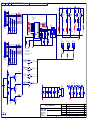
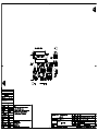
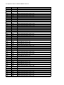
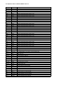
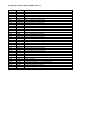
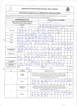
Service
Manual
Issue 1.0
P1 AmpliÞer
ARCAM
Bringing music & movies to life
Contents List
!
Circuit description
!
Circuit diagrams
o L929AY switch PCB
o L962AY amplifier main PCB
!
Transformers
o L929TX – 115/230VAC toroidal
o L927TX – 100VAC toroidal
o L907TX – 100VAC frame
!
Exploded view diagram
!
Mechanical & packing parts list
!
Circuit board silk screen & parts list
o L929AY switch PCB
o L962AY amplifier main PCB
Fmj P1 Amplifier circuit description by A.Moore
Power supply/Control description
Product description
The mains input is applied via SKT1. Y
capacitors C1 and C2 and X capacitor, C5
provide filtering and EMC suppression R2
provides a discharge path for the capacitors.
The P1 has been has been designed to
provide unsurpassed sound quality, the main
design features are as follows.
o
Gain switchable between Arcam gain
and THX gain (29dB closed loop) a 0dB
signal equates to 100 watts into 8
ohms.
o
Input switchable between unbalance
phono and balance XLR.
o
The amp is capable of producing >180
watts of sinusoidal output into an 8
ohm load and greater than 300 watts
into a 3.2 ohm load (subject to thermal
dissipation limits).
o
Relay coupled for silent on/off
operation.
o
Opto-isolated fault and control lines to
the control PCB.
o
DC coupled signal path with
integrating servo to remove residual
DC errors.
o
Instantaneous safe operating area
protection.
o
Exceptionally low harmonic and
intermodulatiion distortion.
o
Flat frequency response.
o
Fast and asymmetric slew rate.
o
High damping factor
o
Unconditionally stable into loads of
upto +/- 90-degree phase.
SW1 allows the selection of the mains voltage
that the unit will operate from, the main standby
transformer TX1 and the main transformer TX2
have duel primary windings, these windings are
connected in parallel for 115v operation and in
series for 230v operation.
TX1 is powered at all times when a mains
voltage is applied to the mains input socket the
secondary of this transformer is fused by via FS3
and rectified by diode bridge DBR1 and
regulated to 5V by low dropout regulator at
location REG2 to provide a constant +5v(D)
supply for the micro.
Please note: the digital supply ground is
connected to the chassis ground via a 100-ohm
resistor.
Relay RLY1 provides a means of powering the
main transformer for normal operation (as
apposed to standby operation where only TX1 is
powered) this relay is under the control of the
Micro IC1 and SW3 on the control board the
relay contacts of RLY1 are suppressed by C3
and C4 these prevent sparking and increase the
relay life span.
The circuitry around TR10 functions as a mains
present detection circuit A.C is feed into this
circuit before the Bridge network at location
DBR1 when mains is present the circuit drives HI
via opto-coupler TR11.
Relay 2 is the speaker output control relay this is
used to prevent clicks and pops at power/power
down and to disconnect the speaker output
under a fault condition, this relay is controlled by
the Micro at location IC1 as the P1 has no
manual speaker switching capabilities the micro
will automatically initialise the speaker relay 3
seconds after power up, the control line SPKR1
on pin 5 of CON 4 switches high to switch the
relay ON via TR9.
The P1 has two trigger inputs these are
applied by SKT2 and are wire OR-ed by D5
and D6. The single trigger signal is clamped
to 4v7 by DZ1 and fed to the control card by
CON4. Applying a 12v trigger signal to
either (or both) trigger inputs on the SKT2
instructs the microcontroller to enable or
disable the power amplifier. The trigger will
be seen as a HI line on Pin 11 of CON 4.
The P1 also provides two 2 triggered
outputs. These are current limited 12v D.C
levels, which are used to provide trigger
signals to other units within the customer’s
installation. The 12v output is present when
transformer TX2 is live i.e. when the unit is
not in standby.
TX2 has a Low voltage secondary winding
that supplies the trigger outputs only via
bridge rectifier DBR4 this is fed into REG1
(7812) regulator, TR1 and TR2 offer a
60mA current limit for both trigger outputs
and the entire circuit stage is fused by FS6
(T315mA) in case of overload.
The P1 utilizes a fairly unique main power
amp power supply configuration these
include.
Fig 1. Power amp power supplies.
Power supply
Powers
+/- 67v D.C
+/- 58v D.C
VAS stage.
Output driver stage.
The two sets of supplies are driven from
their own secondary windings and bridge
rectifier circuits DBR5 and DBR6 Rectify
the +/- 58v rails these are smoothed by
20,000uf of capacitance per phase. DBR2
and DBR3 are supplying the +/- 70v rails
these are dropped to +/- 67 by the Network
of R5, R6, R7, R8 and TR3, TR4, TR5, TR6
this is not a regulated supply as the rails
need to track the +/- 58v rails under mains
power fluctuations.
Please note: The +/- 70v rails are
individually fused by 315mA(T) fuses at
locations FS4 and FS5.
The VAS stage is supplied by higher voltage
rails than the following output driver stage, this
allows the driver stage to fully saturate the
output driver stage without the use of a boot
strap circuit. This supply is exceptionally quite
and is critical to the sound quality of the P1.
Amplifier Stage
The XLR connector at CON100 allows
balanced inputs to be applied to the amplifier
and CON101 allows for the balanced signal to
be daisy chained to a second P1.
The signal from CON100 is driven into IC100
this is a Balanced to single ended converter it
supplies a signal-ended output from a single
XLR input. The IC derives it power supply rails
from the +/- 67v rails these are dropped to
+/- 15v by the TR100 and TR114.
The unbalanced inputs signal arrives at
SKT100; the selection between the two input
options is accomplished by SW100. The
selected signal is clamped +/- 5v3 by the series
Zeners at location DZ103 and DZ104 this is to
prevent damage to the input of op-amp IC200,
due to leaky source signal or electrostatic
discharges.
SW101 allows for the selection of two gain
settings these are 28.3 for “THX” and 37.5 for
the Arcam setting. The roll off setting is
340Khz.
The main power amplifier circuit is a classic
current feed-back design and can be thought of
as a large current feed-back op-amp the
topology is a refined high power output variant
of the A90/P7 design.
Op-amp IC101 is configured as a non-inverting
amplifier with a gain of 2. It’s purpose is to
provide current outputs (via it’s own power
supply pins) and a current input via it’s output
pin, the Op-amp performs the voltage to
current conversion (I-V) and phase splitting
necessary to drive the voltage gain stage. The
current feed-back occurs because the output of
IC101 drives into a 44 ohm load formed by the
two 22 ohm resistors R142 and R143 down to
Cont///
ground, the power
supply pin currents are half wave-rectified
versions of the drive current of the amplifier.
This causes the voltage gain, which is buffered
and passed on to the outputs. The feedback
from pin 1 of IC101 acts to reduce the gain of the
amplifier; when this current is roughly equal to
the current required to drive the input signal into
44-ohm’s equilibrium is reached and the closed
loop gain is defined. The output stage provides
the vast majority of the current required to drive
the 44-ohm load. The op-amp only needs to
provide a very small error current to give the
required voltage magnification.
Transistors TR101 and TR116 are common base
amplifiers their purpose is to provide the +/- 15v
rails necessary to drive the op-amp whilst
allowing the power supply currents that are
drawn to pass through into the Wilson current
mirror stage, this is formed by PNP transistors
TR102, TR104 and TR122 the NPN mirror is
formed by TR115, TR117 and TR122.
TR103 combines the two current mirrors to
provide a very high-gain current to voltage
(transresistance) gain stage roughly 80dB at low
frequency C114 and C132 with R149, R150
combine to give a open-loop pole at roughly
10Khz and a corresponding open-loop zero
around 500Khz. This allows for good time
domain performance and clean square wave
reproduction with no sign of ringing or overshoot.
Diodes D100 and D101 act to limit the current
through TR115 and TR112, if the input current
exceeds 14mA the diodes conduct and the
transresistance stage becomes a constant
current source killing the open loop gain and
preventing damage to the transistors.
IC101 forms a D.C intergrating servo. Its
purpose is to remove residual D.C errors due to
slight device mismatch and component
tolerances. It is configured as an inverting
intergrator with a time constant of <0.5 seconds.
Any D.C offset at the output of the amplifier will
cause the output if the op-amp to go negative
increasing the current in the negative supply pin
SAP
and thus pulling the output down to ground (and
vica versa). D108 protects the inverting input of
the op-amp under fault condition.
TR103 provides a 4.7v bias voltage to allow
the following pre-driver stage to operate in
Class A.
TR123 and TR125 form a Class A pre-driver
emitter follower stage to boost the current gain
and isolate the transresistance stage from the
output transistors. TR105 and TR118 act as a
30mA current limit and prevent the destruction
of TR123 and TR125 under a fault condition.
R109, R164, R110 and R165 loosely decouple
the emitters of TR123 and TR125 from the
output stage.
TR128, TR129 and TR126, TR127 are Sanken
SAP 15N and SAP 15P Bi-polar output drivers
RV100 is the Bias adjust preset D104 protect
the Output drivers from destruction if RV100
goes open circuit.
C144 to C147 provide local R.F stability and
prevent oscillation. D111 and D112 are catch
diodes to reduce the effects of back-EMF from
the loudspeaker coils/load.
R164, R183, C150 and L100 form the Zobel
network, these components ensure that the
amplifier sees a constant load of 4.7 ohms at
high at very high frequencies and improve
stability – reduce H.F noise. L100 and R183
decouple the load at high frequencies to
ensure amplifier stability into capacitive loads.
SAP 15NY
SAP 15PY
S-E 0.22 Ohm
Under output driver failure conditions the 0.22 internal
emitter resistor will usually go open, the resistor should be
measured between pins S and E.
Protection circuit block
The P1 Power amplifier incorporates 4 modes of
protection these are as follows.
o Instantaneous VI current limiting.
RTH100 is low when the amplifier is cool
typically a few hundred ohms, in the event of a
thermal overload situation (Above 110 c)
RTH100 will go into a high impedance state
this will switch TR121 on and intern this will
switch TR111 on and cause OPTO 100C to
send a fault line flag to the micro.
o D.C offset protection.
o Over-Temperature.
o Insulation failure.
The VI current limit circuit is built around TR106
and TR119 they sense the voltage across the
0.22-emitter resistors (hence emitter current) and
the collector emitter current or device power
dissipation exceeds a preset limit.
The circuit is designed to allow large unrestricted
currents into loads of 3 ohms and above but limit
the current into a short circuit or very low
impedance loads.
C141, C142 and R162, R163 form a 2.2ms time
constant, which will allow larger transients of
current delivery for a few milliseconds, to ensure
that the amplifier has a sufficiently large transient
capability to drive “difficult” loudspeaker loads.
TR106 senses positive current surges and
TR119 senses negative surges these intern
activate TR107 and switch the optocoupler
OPTO100A this fault notification is sent to the
microcontroller and the output relay is switched
off to protect the amplifier/loudspeaker coils.
The D.C offset protection is built around TR108
and TR109 a positive D.C offset will switch
TR108, a negative D.C offset will switch TR120
this will intern switch TR110 and TR109 on in
either case this causes the optocoupler at
location OPTO100B to transmit a fault line signal
to the micro.
The Thermistor RTH100 provides Thermal
protection and is connected to the positive
supply rails adjacent to the collector leg of the
output driver at location TR125 this allow the
thermistor to sense the temperature of the output
device. The output impedance of
The remaining protection stage is an
insulation breakdown detect circuit this is
essentially looking for a breakdown of the
insulating pad between the output devices and
the heatsinks thus +60v path to ground.
The protection is formed around bridge rectifier
package DBR100, this will route current
through the LED in optocoupler OPTO 100D in
the event that the DGND and AGND ground
planes move apart by more than 10v. When
the transistor in the Opto conducts the thyristor
formed by TR112 and TR132 is turned On.
Once the Thyristor conducts it pulls the
SHUTDOWN* signal low and turns TR8 (Sheet
2) off thus opening both Speaker relays and
the Power relay.
Please note: The unit can only be reset once
the mains power supply to the unit has been
removed and the Amplifiers own power
supplies have been given sufficient time to
discharge +30 secs. The standby transformer
of course remains active.
TR130 asserts the microprocessor fault line
DCPROT so that the micro can indicate the
fault via the front panel mounted LED.
Fig 2 Fault line location and operational status.
Please note: Con 4 is the connector between
the main board and the display board, use Pin
2 of Con 4 as a reference (DGND).
Fault line
Location
Status
D.C offset
V/I Prot
Thermal
Con 4 Pin 9
Con 4 Pin 8
Con 4 Pin 7
LOW (0v)
LOW (0v)
LOW (0v)
Test Specification
Frequency response. 8-ohm load
Major component identification.
FMMT 497/597
Input set to 1v rms
20Hz – 20kHz = +/- 0.5 dB.
Distortion. THD+N 0dBR 4-ohm load.
BC849/BC859
Input set to 1v rms.
20Hz – 20Khz = <0.02%
Maximum output into an 8-ohm load.
Input level set to 1.34 rms 1Khz = 180 watts
distortion should be below 0.05% THD+N
1=Base
2=Emitter
3=Collector
TLO 72
Bias setting notes
The bias of the P1 is set using an Audio
precision audio analysis package and we
calibrate the power stage for minimum THD the
bench set up procedure follows.
SSM2143
o Set the input signal to 150mv rms,
frequency to 10kHz. Induce a 4-ohm load
at the speaker output.
o Rotate preset RV100 clockwise and
observe that the THD falls. Continue to
rotate the preset until the THD falls to a
minimum level and just starts to clime
again.
o Switch input signal off and allow the
amplifier the Quiesce +30secs
o Measure the bias level at test point Con
103 (Bias read) and confirm the reading is
below the absolute max of 35mV.
74HC32N
ITEM1
1
L929PB
Blank PCB P35/P1 FMJ Amp Microcontroller Board
+5V_D
0V_D
THERMPROT
+5V_D
14
13
12
11
10
9
8
7
6
5
4
3
2
1
SPARE2
STANDBY
SPKR1 ON
SPKR2 ON
THERMPROT 2
VIPROT 2
DCPROT 2
AC PRESENT
TRIGGER
REMOTE
MOLEX
5229-NAPB
R9
R10
R11
R26
10K
0W25
MF
10K
0W25
MF
10K
0W25
MF
10K
0W25
MF
LK1
LK2
0R0
0W25
MF
0R0
0W25
MF
0V_D
100UF
25V
YK
R17
R19
470R
0W25
MF
THERMPROT 1
IC2A
1
THERMPROT 2
2
VIPROT 1
74HC32N
DIP-14
IC2B
4
VIPROT 2
5
DCPROT 1
74HC32N
DIP-14
IC2C
9
TR5
10K
0W25
MF
D2
1N4148
DO-35
SPKR2 ON
100N
50V
X7R
10UF
50V
YK
470R
0W25
MF
0V_D
10
SPARE1
74HC32N
DIP-14
IC2D
12
SPARE2
13
3
THERMPROT
6
VIPROT
8
DCPROT
11
SPARE
470R
0W25
MF
180R
0W25
MF
3mm
BICOL
LED 3mm
LED3
RED
GRN
SW3
SKHVPB000A
0V_D
FIX1
C2
C3
100N
50V
X7R
100N
50V
X7R
C6
C4
100UF
25V
YK
100N
50V
X7R
C7
100UF
25V
YK
1
VCC
7
GND
FIX3
1
Dia 3.5mm
C8
100UF
25V
YK
FIX2
Dia 3.5mm
FIX4
1
FIX5
1
Dia 3.5mm
Dia 3.5mm
1
Dia 3.5mm
C9
C10
C11
C12
C13
100N
50V
X7R
100N
50V
X7R
100N
50V
X7R
100N
50V
X7R
100N
50V
X7R
TR7
0V_D
0V_D
BC546B
TO-92
0V_D
DRAWING TITLE
P35 / P1 Switch PCB
ARCAM
TOOL2
SW2
SKHVPB000A
IC2E
74HC32N
DIP-14
14
STANDBY
R21
TOOL1
SW1
SKHVPB000A
BC546B
TO-92
0V_D
330R
0W25
MF
R8
10K
0W25
MF
0V_D
74HC32N
DIP-14
TR6
10K
0W25
MF
0V_D
C5
+5V_D
R20
R18
DCPROT 2
BC546B
TO-92
0V_D
C1
5mm
GRN
LED 5mm
R15
2
FOR P35 - LEAVE LK1 INTACT
FOR P1 - CUT LINK
SPKR1 ON
C14
1N4148
DO-35
R16
100K
0W25
MF
5mm
GRN
LED 5mm
LED2
R14
LINK LK1 IS USED
TO CONFIGURE PCB
FOR USE IN P35 OR P1
0V_D
+5V_D
0V_D
D1
1
SP2 SW
CON2
3
PWR RED
10K
0W25
MF
LED1
560R
0W25
MF
1
10K
0W25
MF
X1
4.00MHz
SIL-3
+5V_D
560R
0W25
MF
TO-92
R6
10K
0W25
MF
PWR SW
10K
0W25
MF
DCPROT
VIPROT
SP2 LED
PWR GRN
PWR RED
SPARE
R13
2
10K
0W25
MF
28
PB5
PB6
27
PB4
PB7
26
PA3
PA4
25
PA2
PA5
24
PA1
PA6
23
PA0
PA7
22
PB3
OSC2
21
PB2
OSC1
20
PB1
VDD
19
PB0
RES
18
VSS
PC5
17
(TMR)/INT
PC4
16
PC0
PC3
15
PC1
PC2
R4
10K
0W25
MF
SP1 LED
R25
1
2
3
4
5
6
7
8
9
10
11
12
13
14
R12
1
R24
SP2 SW
SP1 SW
SP1 LED
SPKR2 ON
SPKR1 ON
STANDBY
PWR SW
REMOTE
TRIGGER
AC PRESENT
TO-92
R2
10K
0W25
MF
R7
10K
0W25
MF
TR3
BC556B
BC556B
TO-92
SP1 SW
R23
IC1
HT48R30A-1
L019SW
DIP-28
1
R22
TR2
BC556B
TO-92
2
MOLEX
5229-NAPB
TR1
R5
10KTR4
0W25
BC556B
MF
2
SPARE1
STANDBY
SPKR1 ON
SPKR2 ON
THERMPROT 1
VIPROT 1
DCPROT 1
AC PRESENT
TRIGGER
REMOTE
R3
10K
0W25
MF
PWR GRN
R1
10K
0W25
MF
+5V_D
14
13
12
11
10
9
8
7
6
5
4
3
2
1
SP2 LED
CON1
A & R Cambridge Ltd.
Pembroke Avenue
Waterbeach
Cambridge CB5 9PB
Filename:
L929CT_1.0.sch
Notes:
03_E125
KAL
8/05/03
Redrawn, LED1, 2 swapped, Connectors rewired, LK1, 2 added
1.0
03_E001
WAF
2/01/02
HOLTEK, Z1 UPDATED
B.1
JR
1/11/01
ECO No.
Contact Engineer:
Kevin Lamb
Contact Tel:
(01223) 203243
INITIALS
DATE
Printed:
13-May-2003
LEDS TO 5MM AND MAINS SWITCH
B.0
DESCRIPTION OF CHANGE
Sheet
1
of
1
ISSUE
A3
DRAWING NO.
L929CT
ITEM
L962CT3_2
L962CT3_2.0_Power Amplifier.sch
PART No.
DESCRIPTION
NOTES
ITEM1
1
F006
Clip For SW Profile Heatsink
Clip for REG1
ITEM2
1
F022
Fuseholder Cover For 20mm Fuseholder
Cover For FHLDR1
ITEM3
1
F022
Fuseholder Cover For 20mm Fuseholder
Cover For FHLDR2
ITEM4
1
F022
Fuseholder Cover For 20mm Fuseholder
Cover For FHLDR3
ITEM5
1
F022
Fuseholder Cover For 20mm Fuseholder
Cover For FHLDR4
ITEM6
1
F022
Fuseholder Cover For 20mm Fuseholder
Cover For FHLDR5
ITEM7
1
F022
Fuseholder Cover For 20mm Fuseholder
Cover For FHLDR6
ITEM8
1
L962PB
Blank PCB P1 Amplifier Main Board
ITEM9
2
E802AP
Pad Damping 15x6x3MM Sorbothane
See Assy Drawing for location
ITEM10
3
E826AP
Pad Damping 7.5x6x3 Sorbothane
See Assy Drawing for location
ITEM11
1
8M101
Earth Lead Assy 75MM
L962CT2_2
L962CT2_2.0_PSU and Control.Sch
VIPROT
DC
THERM
SHUTDOWN*
FIX1
QTY
VIPROT
DC
THERM
SHUTDOWN*
FIX2
FIX5
1
FIX6
FIX9
FIX10
FIX13
1
CHASSIS1
Dia 3.2mm
Dia 3.2mm
Dia 3.5mm
Dia 3.5mm
Dia 3.5mm
Dia 3.5mm
Dia 3.5mm
FIX3
FIX4
FIX7
FIX8
FIX11
FIX12
FIX14
Dia 3.5mm
Dia 3.5mm
Dia 3.5mm
FD1
FD2
1
1
FD3
FD4
Dia 3.5mm
CHASSIS1
CHASSIS2
Dia 3.5mm
Dia 3.5mm
Dia 3.5mm
TOOL1
TOOL2
DRAWING TITLE
P1 Amplifier Main PCB
TOOL3
TOOL4
23425
A & R Cambridge Ltd.
Pembroke Avenue
Waterbeach
Cambridge CB5 9PB
Filename:
L962CT1_2.0.Sch
Notes:
Contact Engineer:
Kevin Lamb
Contact Tel:
03_E249
KAL
22/08/03
Stability mods
2.0
03_E203
KAL
16/07/03
Production Release, VI Limiting changes
1.0
03_E184
KAL
23/06/03
Changed sorbothane part numbers, corrected R179-182, R185-187
B.1
03_E111
KAL
11/04/03
Corrected CON4, Redesigned protection cct and voicing mods
B.0
03_E055
KAL
18/02/03
ECO No.
INITIALS
DATE
Printed:
22-Aug-2003
(01223) 203243
Minor Change to re-label gain switch positions
A.1
DESCRIPTION OF CHANGE
Sheet
1
of
1
ISSUE
DRAWING NO.
L962CT1
NEUTRAL
TX1
Open Frame
1
MAINS PRESENT DETECT
5
D3
BAS16
SOT-323
EARTH
C2
3N3
250V
CER
L
2B
2A
C5
220N
275V
PP X2
115V
R2
1M5
0W5
VR37
230V
SKT1
BULGIN
PX0580
2
6
3
7
HS1A
SW50-2
8.8C/W
FS3
T315mA
S504
FHLDR3
20mm HLDR
115V
FS1 T6.3A S506
9V
C11
100N
50V
0805
CON1
REG2
L4940V5
TO-220
GREEN
1
LIVE
RLY1B
Takamisawa
F1CA005V
C12
100N
50V
0805
C21
3300UF
25V
YK
8
FHLDR2
20mm HLDR
WAGO
256
+5V(D)
DBR1
W02G
FS2 T6.3A S506
4
R15
10K
0W25
1206
C33
1000UF
10V
YK
C13
100N
50V
0805
TR10
BC849B
SOT-23
CON3
TX WIRE COLOURS
4
C4
3N3
250V
RLY1A
F1CA005V
Takamisawa
P4
1
5
2
6
3
TR11
MMUN2211LT1
SOT-23
C36
D6
BAS16
SOT-323
CER
R17
4K7
0W25
1206
P3
C3
3N3
250V
MAINS WIRING AND AUXILIARY SUPPLY
R16
2K2
0W25
1206
+5
FHLDR1
20mm HLDR
SW1
18-000-0019
+5V(D)
9V
115V
1B
E
1
N
1A
C1
3N3
250V
CER EARTH
2
EMC Shield
SH1
100UF
25V
YK
DGND
DGND
1 BLUE
3 BROWN
4 BLACK
6 WHITE
MOLEX
44472
CER
D4
BAS16
SOT-323
VP70V
VP58VAC1
VP58VAC2
VN58VAC1
VN58VAC2
4
9
3
8
2
7
1
6
1 GREEN
2 YELLOW
3 ORANGE
4 RED
5 WHITE
6 GREY
7 VIOLET
8 BLACK
9 BROWN
10 BLUE
VN70VAC1
VP70VAC2
VP70VAC1
VP18VAC2
VP18VAC1
VP70VAC1
FHLDR4
20mm HLDR
C14
2K2
0W25
1206
VP58VAC2
TR4
FMMT497
SOT-23
C24
C25
R19
C28
C30
C19
R13
10,000UF
71V
AM
10,000UF
71V
AM
10K
1W
CF
47UF
100V
YK
47UF
100V
YK
100N
100V
MKS2
68K
0W25
1206
100N
100V
MKS2
C34
100UF
100V
YXF
2K2
0W25
1206
DBR5
GBU8D
D1 BAS16
SOT-323
TR3
2SA1930
TO-220
R6
C15
+5V(D)
RLY1C
Takamisawa
F1CA005V
AGND_C2
DBR6
GBU8D
P1
AGND_PSU3
NC2
D2 BAS16
SOT-323
VN58VAC1
C6
100P
100V
0805
C16
EMCGND
VN58VAC2
C27
R20
C29
C31
C20
R14
10,000UF
71V
AM
10,000UF
71V
AM
10K
1W
CF
47UF
100V
YK
47UF
100V
YK
100N
100V
MKS2
68K
0W25
1206
R7
VN58V
+12V(D)
FHLDR5
20mm HLDR
VN70VAC2
TR1
BD179
TO-126
R3
3K3
0W25
1206
TR2
FMMT497
SOT-23
1000UF
100V
YK
C17
100N
100V
MKS2
+18V(D)
+12
R8
C8
R4
100N
50V
0805
100N
50V
0805
2K2
0W25
1206
TR6
2SC5171
TO-220
D5
VN70V
TR8
FMMT497
SOT-23
VN67V
P7
BAS16
SOT-323
C18
VP18VAC1
DGND
R1
10R
0W25
1206
DC
100N
100V
MKS2
2K2
FMMT497 0W25
SOT-23 1206
P6
SHUTDOWN*
C32
1000UF
35V
YK
FS6
T315mA
S504
R11
P8
DGND
+18V(D)
VP18VAC2
2K2
0W25
1206
100UF
100V
YXF
2K2
0W25
1206
R9
TR7 2K2
FMMT497 0W25
SOT-23 1206
R10
C35
DBR4
W02G
C7
+5V(D)
C23
VN70VAC1
D8
BAS16
SOT-323
TR9
P5
TR5
FMMT597
SOT-23
2K2
0W25
1206
DBR3
W02G
RLY2B
Omron
G2R-1-E-12VDC
D7
BAS16
SOT-323
AGND_PSU1
C26
100N
100V
MKS2
FS5
T315mA
S504
REG1
L7812CV
TO-220
AGND_PSU2
AMPLIFIER
MUTING
RELAY
+12V(D)
AGND_C1
NC1
GND2
GND1
1000UF
100V
YK
VP58V
VP58VAC1
SKT3
HOSIDEN
HSJ
R5
100N
100V
MKS2
VP70VAC2
MOLEX
44472
SKT2
HOSIDEN
HSJ
C22
VIPROT
DGND
THERM
DCPROT
VIPROT
THERMPROT
+5V(D)
FHLDR6
20mm HLDR
TRIGGER
AC PRESENT
NC1
C9
100N
50V
0805
AGND_PSU2
SPKR2 ON
SPKR1 ON
STANDBY*
SP1
GND2
GND1
NC2
L1
DZ1
BZX84C
4V7
SOT-23
R18
10K
0W25
1206
AGND_SIG
AGND_C1
AGND_PSU1
AGND_LS
AGND_PSU3
AGND_C2
70R@100MHz
C10
100N
50V
0805
CHASSIS1
DGND
R12
P2
100R 0W25
1206
CHASSIS2
DGND
AGND_RC
CON4
14
13
12
11
10
9
8
7
6
5
4
3
2
1
TO DISPLAY CARD
VN70VAC2
10
DBR2
W02G
FS4
T315mA
S504
TX WIRE COLOURS
CON2
5
VP67V
DGND
MOLEX
5229-NCPB
DRAWING TITLE
P1 Amplifier Main PCB
23425
A & R Cambridge Ltd.
Pembroke Avenue
Waterbeach
Cambridge CB5 9PB
Filename:
L962CT2_2.0_PSU and Control.Sch
Notes:
03_E249
KAL
22/08/03
Stability mods
2.0
03_E203
KAL
16/07/03
Production Release, VI Limiting changes
1.0
03_E184
KAL
23/06/03
Changed sorbothane part numbers, corrected R179-182, R185-187
B.1
03_E111
KAL
11/04/03
Corrected CON4, Redesigned protection cct and voicing mods
B.0
03_E055
KAL
18/02/03
Minor Change to re-label gain switch positions
INITIALS
DATE
Printed:
22-Aug-2003
ECO No.
Contact Engineer:
Kevin Lamb
Contact Tel:
(01223) 203243
A.1
DESCRIPTION OF CHANGE
Sheet
2
of
3
ISSUE
DRAWING NO.
L962CT1
VP67V
C109
R125
R133
D100
C113
C122
R135
47R
0W25
1206
BAS16
SOT-323
100N
100V
MKS2
47UF
100V
YK
47R
0W25
1206
NF
6K8
0W25
MF
TR100
CON101
Neutrik
NC3FBH2-B
R126
C120
6K8
0W25
MF
47UF
100V
YK
P105
AGND_SIG
AGND_PSU1
TR115
FMMT597
SOT-23
AGND_PSU1
2
2
2
2
+15VD
1
3
VCC
G
3
G
2
3
SNS
VO
C100
100N
50V
0805
5
AGND_SIG
P101
C127
C135
1
AGND_SIG
6U8 63V
MKS4
AGND_PSU1
AGND_SIG
BAV99
SOT-23
C128
100UF
25V
CFNE
FMMT497
SOT-23
R101
-15VD
SW100A
SPUN191400
NC1
SELECT PHONO
C2
NO1
NO2
C130
10R 0W25
1206
SW100B
SPUN191400
NC2
C1
C136
TR101
C101
100N
50V
0805
6K8
SW101A
SPUN191400
NC1
P7 GAIN
ARCAM GAIN
22UF
20V
OSCON
DZ102
NF
C2
NO1
NO2
C110
C103
C137
100N
100V
MKS2
100N
50V
0805
10N
50V
0603
P122
100R
0W25
1206
2K2
0W25
1206
AGND_SIG
REF100
LM431AIM3
SOT-23
AGND_SIG
0W25
1206
5
BZX84C
4V7
SOT-23
6K8
0W25
MF
SCRN
1
2
CON102
NF
DZ101
C129
BZX84C
4V7
SOT-23
470P
100V
FKP2
3
8
R129
47P
200V
0805
TR126
SAP15NY
SAP
C146
150R
0W25
1206
47P
200V
0805
TR127
SAP15NY
SAP
IC101A
TL072CD
SO-8
1
D108
BAV99
SOT-23
C116
C133
100N
100V
MKS2
22UF
20V
OSCON
R139
1K0
0W25
1206
R153
Trim output stage Iq
AGND_SIG
R138
R142
22R
0W25
MF
R132
22K
0W25
MF
1K5
D104
RV100
100R
BAS16
LIN
SOT-323
C117
C134
100N
100V
MKS2
22UF
20V
OSCON
Measure Iq
1K0
0W25
1206
R143
22R
0W25
MF
1K8
22UF
20V
OSCON
AGND_SIG
NF
HARWIN
M20-973
0W25
MF
P109
R131
12K
0W25
1206
0W25
MF
1K8
1K5
0W25
MF
R147
0W25
MF
1K8
0W25
MF
R149
6K8
0W25
1206
C114
C132
100N
100V
MKS2
22UF
20V P114
OSCON
R150
1K0
0W25
1206
REF101
LM431AIM3
SOT-23
100R 0W25
1206
P102
TR114
1N0
100V
FKP2
C111
C104
C138
100N
100V
MKS2
100N
50V
0805
10N
50V
0603
AGND_SIG
AGND_SIG
AGND_SIG
33P
R127
C121
6K8
0W25
MF
47UF
100V
YK
R176
150R
0W25
1206
TR118
FMMT597
SOT-23
AGND_SIG
P111
TR102
FMMT497
SOT-23
C150
47N
100V
MKS2
R178
150R
0W25
1206
C145
47P
200V
0805
C147
47P
200V
0805
BASE2
P125 100R
0W25
1206
AGND_PSU3
P126
TR104
TR123
FMMT497
SOT-23
2SA1740
SOT-89
C119
C125
100N
100V
MKS2
47UF
100V
YK
D112
1N4003
DO-41
D110
AGND_PSU1
AGND_PSU1
C112
P116
R134
D101
C115
C123
R136
47R
0W25
1206
BAS16
SOT-323
100N
100V
MKS2
47UF
100V
YK
47R
0W25
1206
NF
AGND_RC
TR129
SAP15PY
SAP
R165
22R
0W25
1206
R110
4B4548
SOT-89
R128
6K8
0W25
MF
R161
TR124
P110
1K0
0W25
1206
EMITTER2
TR128
SAP15PY
SAP
250V
PP
P115
AGND_LS
P123
P124
6K8 0W25
1206
AGND_PSU1
FMMT597
SOT-23
FMMT497
SOT-23
C140
R103
CHASSIS1
R155
TR103
22R
0W25
1206
TR116
FMMT597
SOT-23
Omron
G2R-1-E-12VDC
R184
4R7
2W
CF
1K0
0W25
1206
150K
0W25
MF
R141
0W25
MF
R146
1K8
0W25
MF
P104
2K2
0W25
1206
10R 2W
CF
OUTPUT
R154
R105
R106
RLY2A
R183
R145
R140
1K5
DZ103
NF
1K5
L100
2U2
CON103
1
2
R169
AGND_SIG
C131
0W25
MF
R144
C102
NF
AGND_PSU1
LS100
G P PRECISION
EMITTER1
2
100R
0W25
MF
AGND_SIG
C126
150R
0W25
1206
R177
P108
R192
CHASSIS1
C144
R152
GAIN=37.0
AGND_PSU1
P100
BASE1
R175
150K
0W25
MF
P107
0R0
0W25
1206
4
DZ100
SKT100
KUNMING
GOLD
1N4003
DO-41
R137
R123
R124
D111
47UF
100V
YK
R168
AGND_SIG
820R
0W25
MF
C124
100N
100V
MKS2
P131
33P 250V
PP
1M0 0W25
1206
R118 IC101B
4K7
TL072CD
0W25 SO-8
1206
AGND_SIG
C118
AGND_PSU3
22R
0W25
1206
R148
6
AGND_PSU1
GAIN=28.3
R164
NF
7
P103
R104
SW101B
SPUN191400
NC2
C1
R130
12K
0W25
1206
P121
C139
R102
VP58V
R109
4B1740
SOT-89
6
-15VD
SELECT XLR
TR122
P113
4
VEE
REF
2SC4548
SOT-89
TR105
FMMT497
SOT-23
10R
0W25
1206
100UF
25V
CFNE
AGND_PSU1
FMMT597
SOT-23
FMMT497
SOT-23
IN+
D107
BAV99
SOT-23
IC100
SSM2143S
SO-8
IN-
+15VD
D106
R100
1
3
7
3
TR125
VN58V
SBYV27-200
DO-15
VN67V
D102
BASE1
P118
P127
VP58V
BAS16
SOT-323
R116
18K
0W25
1206
OPTO100A
PC3Q66Q
MINI-FLAT
P117
R188
R166
2K2
0W25
1206
P157
R107
R162
DZ105
330R
0W25
1206
1K0
0W25
1206
BZX84C
33V
SOT-23
R108
R163
DZ106
330R
0W25
1206
1K0
0W25
1206
BZX84C
33V
SOT-23
C142
R111
P128
100R
0W25
1206
C105
EMITTER2
3
14
4
13
+5V(D)
5
12
6
11
R179
270R
0W25
1206
RTH100
PTC 110DEG
PTC
P149
4K7
0W25
1206
DGND
R172
P137
R121
22K
0W25
1206
R180
4K7
0W25
1206
DGND
P138
TR121
R122
22K
0W25
1206
4K7
0W25
1206
DGND
P146
TR111
D105
P134
P135
P147
P150
TR130
MMUN2111LT1
SOT-23
100K
0W25
1206
C143
DZ104
BZX84C
15V
SOT-23
FMMT597
SOT-23
R181
R186
10K
0W25
1206
120K
0W25
1206
100UF
25V
YK
VIPROT
BAS16
P139
TR108
FMMT497
FMMT497
SOT-23
SOT-23
R182
R187
10K
0W25
1206
39K
0W25
1206
DC
THERMPROT
FMMT497
SOT-23
Over temperature sensing
+5V(D)
THERM
+5V(D)
AGND_PSU3
TR131
MMUN2111LT1
SOT-23
TR120AGND_PSU3
R170
VIPROT
DCPROT
SOT-323
TR107
P153
FMMT597
R113
22K
0W25
1206
C106
100N
50V
0805
P129
TR119
FMMT597
SOT-23
P140
P130
SOT-23
C148
C149
R120
R173
R174
100UF
16V
NONP
100UF
16V
NONP
4K7
0W25
1206
22K
0W25
1206 P141
22K
0W25
1206
AGND_PSU3
P142
DBR100
W02G
C108
OPTO100D
DGND
DC offset detection
C151
100N
50V
0805
AGND_PSU3
TR109
7
R158
1K0
0W25
1206
P154
SHUTDOWN*
TR132
BC859B
SOT-23
P152
1K0 0W25
1206
P155
PC3Q66Q
MINI-FLAT
TR113
MMUN2211LT1
SOT-23
R160
1K0
0W25
1206
TR112
BC849B
SOT-23
1K0
0W25
1206
DZ107
P144
P158
BZX84C 6V8
SOT-23
R117
R114
R115
18K
0W25
1206
100R
0W25
1206
100R
0W25
1206
D103
R159
SOT-23
Instant SOA limiting
BASE2
9
P151
100N
50V
0805
R156
TR110
FMMT497
SOT-23
0W25
1206
10
8
P148
FMMT497
R191
P143
VN58V
P145
+5V(D)
R157
1K0
0W25
1206
P156
2K2
P120
R119
R151
1K0
0W25
1206
100N
50V
0805
R190
18K
0W25
1206
P136
P133
R112
100R
0W25
1206
1K2
0W25
1206
15
R171
SOT-23
100R 0W25
1206
10UF
50V
YK
R167
2
TR106
FMMT497
OUTPUT
16
22K
0W25
1206
C141
10UF
50V
YK
P132
100N
50V
0805
18K
0W25
1206
1K2
0W25
1206
1
OPTO100C
PC3Q66Q
MINI-FLAT
+5V(D)
R185
C107
R189
EMITTER1
OPTO100B
PC3Q66Q
MINI-FLAT
+5V(D)
THERMPROT
1
SBYV27-200
DO-15
TR117
DCPROT
1
D109
P112
AGND_PSU1
P106
VIPROT
CON100
Neutrik
NC3MBH-B
DRAWING TITLE
P1 Amplifier Main PCB
23425
Filename:
DGND
60V DC Output Fault Detect
L962CT3_2.0_Power Amplifier.sch
Notes:
03_E249
KAL
22/08/03
Stability mods
2.0
03_E203
KAL
16/07/03
Production Release, VI Limiting changes
1.0
03_E184
KAL
23/06/03
Changed sorbothane part numbers, corrected R179-182, R185-187
B.1
03_E111
KAL
11/04/03
Corrected CON4, Redesigned protection cct and voicing mods
B.0
03_E055
KAL
18/02/03
Minor Change to re-label gain switch positions
P119
BAS16
SOT-323
A & R Cambridge Ltd.
Pembroke Avenue
Waterbeach
Cambridge CB5 9PB
ECO No.
Contact Engineer:
Kevin Lamb
Contact Tel:
(01223) 203243
INITIALS
DATE
Printed:
22-Aug-2003
A.1
DESCRIPTION OF CHANGE
Sheet
3
of
3
ISSUE
DRAWING NO.
L962CT
120mm dia max
Transformer Specification For 115/230V P1 transformer
SECONDARIES
Connector Latch
1mm
Arcam Part Number L926TX
COUNTERBORE DIA 25mm
BLACK
8
1. Winding Wire to be Grade 2 (130C rating) to BS 60317-4 1995
6
5
4
10 9
8
7
6
3
2
1
5
3
2
1
4
Lid
PRIMARIES
2. Mylar Polyester Insulator 130C Rated
6 way
4
78mm max
50mm
40mm
BLACK
YELLOW
2
115Vac
GREY
VIOLET
BLACK
BROWN
1
GREEN
BLUE
10
50.8Vac
7mm DIA HOLE
VN70V
5
WHITE
SCREEN WIRE GREEN/YELLOW
GREY
Rubber insulating pad to have
7mm minimum diameter hole through centre
6
1
14.35Vac
VP18V
7
VIOLET
GREEN
2
YELLOW
3
ORANGE
RED
4
5
BLUE
WHITE
1
2
VN58V
43.0Vac
6
7
8
9
10
BLUE
BLACK
4
WHITE
5
6
3
BROWN
3
4
POTTING COMPOUND
Wires to exit from near top of TX
Such that wires do not obstruct lid
Rubber insulating pad
4. All wire lengths in mm. Lengths are +5.0, -0
VP58V
ORANGE
BLUE
Note Lid is only 1mm above top
face of max height transformer
Equivalent Conexcon 6740 Series UL94V0 parts may be used.
6 Way receptacle 6740-1060
10 Way receptacle 6740-1100
3. Primary wires are enclosed in a common sleeve. Secondary wires are
enclosed in a common sleeve.
Use UL rated sleeving.
43.0Vac
WHITE
1
Note Molex UL94V0 receptacles may be long lead time items.
RED
115Vac
6
6 Way Molex
2. Primary windings connect to 6 way MOLEX connector 39-01-2065.
Secondary
windings connect to 10 way molex connector 39-01-2105. Use MOLEX pin
44476-3112.
MOLEX connectors have pin numbers indicated on them. Connectors to be
UL94V0 rated.
9
BROWN
3
Pin outs of Molex connectors
As viewed looking down at the end
the wires enter the connector
1. Centre of transformer to be potted (as shown).
VP70V
BROWN
10 way
3. Potting Compound PC3502 E135297(M) or equivalent.
Mechanical Specification
50.8Vac
10 Way Molex
Material Safety Specification
5. Please adhere rubber insulating pad to bottom of transformer as shown.
Electrical Specification
1. Transformer to have dual 115V primaries to allow parallel operation for
115V input and series operation with 230V input.
200mm
2. Transformer input voltage range
Secondary Winding Voltage and Current Specs
Bridge Rectifier Vf diode = 1.1V per leg = 2.2V Total
(ideal TX assumed)
115V -18% +14% (97.5V to 132.5V)
230V -18% +14% (195V to 265V)
3. Transformer to have 5 secondary windings as show in the adjacent
drawing.
AC Winding
Label
4. Loaded DC voltages specified at 230V AC in (with transformer primaries
in series)
5. Each secondary winding to have a full wave (4diode) bridge to produce a
single DC rail.
(AS shown in diagram)
Capacitor
Cout
Effective DC
Load Current
(uF)
(mA)
Secondary
Voltage
(V r.m.s.)
Capacitor
Peak Voltage
Vpk
(Volt)
160mm
SCREEN WIRE
Capacitor
Min Voltage
Vmin
(Volt)
Capacitor
Average
Voltage
(Volt)
Load Resistor
to simulate
Load RL
(Ohm)
Secondary
Winding r.m.s.
Current
(A r.m.s.)
1400
25.6
25.6
1400
102.8
0.25
8.0
8.0
0.25
0.52
PRIMARIES
6 way MOLEX MFIT JNR
VP70V
VP58V
VN58V
VN70V
VP18V
6. Output Capacitance to be as specified per rail.
7. Output voltages to be as specified in table and as shown in diagram.
1000
20,000
20,000
1000
1000
50
2250
2250
50
175
50.8
43.0
43.0
50.8
14.35
70.2
58.8
58.8
70.2
18.75
69.8
57.8
57.8
69.8
17.25
70.0
58.3
58.3
70.0
18.0
8. Note. Transformer to be used in a power amplifer. The specified load
currents on the high power rails (VP58V, VN58V) represent the effective
current drawn when the amplifier is loaded to full rated power (200W) into
an 8ohm load and operated continuously.
This load current is not typical of normal operation which is considered to be
1/8th of full rated power.
90 degree
SECONDARIES
10 way MOLEX MFIT JNR
Voltage on Reservoir Capacitor
Vpk
Vaverage
Vmin
10mS
130mm
TEST CIRCUIT
Vf = 1.1V
per diode
+VOUT
AC IN
DRAWING TITLE
+
Cout
POWER TX FOR P1 115/230V
RL see above table.
ARCAM
GND
A & R Cambridge Ltd.
Pembroke Avenue
Waterbeach
Cambridge CB5 9PB
Filename:
L926TX_1.0.sch
Notes:
03_E240
KAL
Reduced VP58V, VN58V to 43.0Vac
1.0
03_E193
SLS
'UL rated sleeving' was 'UL94-V0'
B.3
03_E192
KAL
Added note about UL94-V0 sleeving
B.2
03_E158
KAL
Corrected Schematic Symbol pin numbers
B.1
03_E141
ECO No.
Contact Engineer:
Kevin Lamb
Contact Tel:
(01223) 203243
KAL
INITIALS
Printed:
Changed Pri wire colours, VP58 and VN58 +1V, lead out forms
DATE
7-Aug-2003
DESCRIPTION OF CHANGE
Sheet
1
of
1
B.0
ISSUE
A3
DRAWING NO.
L926TX
120mm dia max
Transformer Specification For 100V P1 transformer
SECONDARIES
Connector Latch
1mm
Arcam Part Number L927TX
COUNTERBORE DIA 25mm
BLACK
8
1. Winding Wire to be Grade 2 (130C rating) to BS 60317-4 1995
6
5
4
10 9
8
7
6
3
2
1
5
3
2
1
4
Lid
PRIMARIES
2. Mylar Polyester Insulator 130C Rated
6 way
4
78mm max
50mm
40mm
BLACK
YELLOW
2
100Vac
GREY
VIOLET
BLACK
BROWN
VN58V
1
GREEN
BLUE
10
50.8Vac
7mm DIA HOLE
VN70V
5
WHITE
SCREEN WIRE GREEN/YELLOW
GREY
Rubber insulating pad to have
7mm minimum diameter hole through centre
6
1
14.35Vac
VP18V
7
VIOLET
GREEN
2
YELLOW
3
ORANGE
RED
4
5
BLUE
WHITE
1
2
43.3Vac
6
7
8
9
10
BLUE
BLACK
4
WHITE
5
6
3
BROWN
3
4
POTTING COMPOUND
Wires to exit from near top of TX
Such that wires do not obstruct lid
Rubber insulating pad
4. All wire lengths in mm. Lengths are +5.0, -0
VP58V
ORANGE
BLUE
Note Lid is only 1mm above top
face of max height transformer
Equivalent Conexcon 6740 Series UL94V0 parts may be used.
6 Way receptacle 6740-1060
10 Way receptacle 6740-1100
3. Primary wires are enclosed in a common sleeve. Secondary wires are
enclosed in a common sleeve.
Use UL rated sleeving.
43.3Vac
WHITE
1
Note Molex UL94V0 receptacles may be long lead time items.
RED
100Vac
6
6 Way Molex
2. Primary windings connect to 6 way MOLEX connector 39-01-2065.
Secondary
windings connect to 10 way molex connector 39-01-2105. Use MOLEX pin
44476-3112.
MOLEX connectors have pin numbers indicated on them. Connectors to be
UL94V0 rated.
9
BROWN
3
Pin outs of Molex connectors
As viewed looking down at the end
the wires enter the connector
1. Centre of transformer to be potted (as shown).
VP70V
BROWN
10 way
3. Potting Compound PC3502 E135297(M) or equivalent.
Mechanical Specification
50.8Vac
10 Way Molex
Material Safety Specification
5. Please adhere rubber insulating pad to bottom of transformer as shown.
Electrical Specification
1. Transformer to have dual 100V primaries to allow parallel operation for
100V input.
200mm
2. Transformer input voltage range
Secondary Winding Voltage and Current Specs
Bridge Rectifier Vf diode = 1.1V per leg = 2.2V Total
(ideal TX assumed)
100V -15% +15% (85V to 115V)
3. Transformer to have 5 secondary windings as show in the adjacent
drawing.
4. Loaded DC voltages specified at 100V AC in (with transformer primaries
in parrallel)
AC Winding
Label
5. Each secondary winding to have a full wave (4diode) bridge to produce a
single DC rail.
(AS shown in diagram)
Capacitor
Cout
Effective DC
Load Current
(uF)
(mA)
Secondary
Voltage
(V r.m.s.)
Capacitor
Peak Voltage
Vpk
(Volt)
160mm
SCREEN WIRE
Capacitor
Min Voltage
Vmin
(Volt)
Capacitor
Average
Voltage
(Volt)
Load Resistor
to simulate
Load RL
(Ohm)
Secondary
Winding r.m.s.
Current
(A r.m.s.)
1400
25.6
25.6
1400
102.8
0.25
8.0
8.0
0.25
0.52
PRIMARIES
6 way MOLEX MFIT JNR
VP70V
VP58V
VN58V
VN70V
VP18V
6. Output Capacitance to be as specified per rail.
7. Output voltages to be as specified in table and as shown in diagram.
8. Note. Transformer to be used in a power amplifer. The specified load
currents on the high power rails (VP58V, VN58V) represent the effective
current drawn when the amplifier is loaded to full rated power (200W) into
an 8ohm load and operated continuously.
This load current is not typical of normal operation which is considered to be
1/8th of full rated power.
1000
20,000
20,000
1000
1000
50
2250
2250
50
175
50.8
43.0
43.0
50.8
14.35
70.2
58.8
58.8
70.2
18.75
69.8
57.8
57.8
69.8
17.25
70.0
58.3
58.3
70.0
18.0
90 degree
SECONDARIES
10 way MOLEX MFIT JNR
Voltage on Reservoir Capacitor
Vpk
Vaverage
Vmin
10mS
130mm
TEST CIRCUIT
Vf = 1.1V
per diode
+VOUT
AC IN
DRAWING TITLE
+
Cout
POWER TX FOR P1 100V
RL see above table.
ARCAM
GND
A & R Cambridge Ltd.
Pembroke Avenue
Waterbeach
Cambridge CB5 9PB
Filename:
L927TX_1.0.sch
Notes:
03_E240
KAL
Reduced VP58V, VN58V to 43.0Vac
1.0
03_E193
SLS
'100V' text was '115/230V', 'UL rated sleeving' was 'UL94-V0'
B.1
03_E192
KAL
Changed voltages as per L926TX, sleeving to be UL94-V0
B.0
03_E006
ECO No.
Contact Engineer:
Kevin Lamb
Contact Tel:
(01223) 203243
KAL
INITIALS
Printed:
Prototype Release
DATE
7-Aug-2003
A.0
DESCRIPTION OF CHANGE
Sheet
1
of
1
ISSUE
A3
DRAWING NO.
L927TX
P1 Mechanical and packing parts list
Part No
E200AY
E212AY
E822PM1
E907MC
E912MC
E918HK
E921MC
HA3V06A
HA4A12B
HA5K70A
HA5L20B
HA6K50A
HB25V12B
HE6V06B
HF4V09B
HJ4A00A
HL4SB
HL5CA
HL6MA
L915CA
L929AY
L926TX
L927TX
Item no Description
GENERAL MECHANICAL PARTS
4
Rear Panel Assembly FMJ P1
6
FMJ A32 Chassis Assembly
7
Foot Black Alpha
9
Koolpad O/P Device Diva A85
10
Clamp 85 Amp Transistor
11
Heatsink FMJ P1
12
Clamp Heatsink Diva P85 3RD Channel
15
M Screw Torx P/H M3x6MM ST ZP
16
M Screw Pan Supa M4x12MM ST BLK
17
Bolt Hex HD M5x70MM ST ZP
18
M/C Hex HD. Bolt M5-0.8X20MM Steel - Zinc Black Passivate
19
Bolt Hex HD M6x50MM Mczp
20
Screw Taptite M2.5X12MM Pan Torx(T8) Steel Zinc Plate Black
21
Screw Sftp Torx No.6x6MM BLK
22
Screw Self-Tapping-Sems NO.4 X 9MM Pan Torx-Slot Steel Zinc-Plate BLK
23
Nut M4 Full ST ZP
24
Washer M4 Int Shakeproof BLK
25
Bright Washer M5 (Form C) to BS 4320
26
Bright Washer M6 (Mudguard O.D. 20mm)
27
Cable FFC 0.1" 14WAY A85 Disp - Pwr
28
P35/P1 FMJ Amp Microcontroller Board Assembly
29
115/230 VAC Toroid transformer
29
100 VAC only Toroid transformer
E210AYB
HA4V06B
2
3
E189AYB
1
8Q006
E083AY
E199AYB
E830MC
E847PM
E894PMB
HL25AB
E933AY
HA3A04A
E210AY
HA4V06S
2
3
E189AY
1
8Q006
E083AY
E199AY
E830MC
E847PM
E894PM
HL25AB
E933AY
HA3A04A
BLACK CASE PARTS
FMJ P1/P35-3 Black Cover Assembly
M Screw Torx M4x6MM Stainless Steel Black
FMJ Black P1 Fascia Complete Assembly
Made up of the following parts :8Q006 FMJ Tact Button Spring
FMJ A32 Sub-Panel Assy
Front Panel Assembly Black FMJ P1
Badge Metal Arcam FMJ
Lightpipe FMJ
Button Power FMJ A32 Black
HL25AB FMJ Tact Button Fastener
FMJ I/R Window Assy (STD. SCREENED)
M/C Pan Supa M3X4 Stzp
SILVER CASE PARTS
FMJ P1/P35-3 Silver Cover Assembly
M Screw Torx M4x6MM Stainless Steel Silver
FMJ Silver P1 Fascia Complete Assembly
Made up of the following parts :8Q006 FMJ Tact Button Spring
FMJ A32 Sub-Panel Assy
Front Panel Assembly Silver FMJ P1
Badge Metal Arcam FMJ
Lightpipe FMJ
Button Power FMJ A32 Silver
HL25AB FMJ Tact Button Fastener
FMJ I/R Window Assy (STD. SCREENED)
M/C Pan Supa M3X4 Stzp
PACKAGING MATERIAL
E827PK
E828PK
E826PK
E967SL
SH139
E888PM
Carton Printed FMJ
End Caps Pair FMJ A22 / P25 / DT26
Carton Plain FMJ
FMJ P1 Carton Label
Handbook FMJ C30/P35/P1 Multi
Blanking Plug For 4MM Binding Post
P1 Amplifier display cct board L929AY issue 2.0
Designator
Part
Description
C1
C2
C3
C4
C5
C6
C7
C8
C9
C10
C11
C12
C13
C14
CON1
CON2
D1
D2
IC1
IC2
ITEM1-1
ITEM2-1
LED1
LED2
LED3
LK1
LK2
R1
R2
R3
R4
R5
R6
R7
R8
R9
R10
R11
R12
R13
R14
R15
R16
R17
R18
R19
R20
R21
R22
R23
R24
R25
R26
SW1
SW2
SW3
TR1
TR2
TR3
TR4
TR5
TR6
TR7
X1
2A410
2A410
2A410
2A410
2N610
2N710
2N710
2N710
2A410
2A410
2A410
2A410
2A410
2N710
8K7014A
8K7014A
3A4148
3A4148
L019AY
5J7432
L929PB
8S028N
3D001
3D001
3D006
1H000
1H000
1H310
1H310
1H310
1H310
1H310
1H310
1H310
1H310
1H310
1H310
1H310
1H156
1H156
1H133
1H118
1H410
1H310
1H310
1H147
1H147
1H147
1H310
1H310
1H310
1H310
1H310
A1504
A1504
A1504
4A556
4A556
4A556
4A556
4A546
4A546
4A546
7W005
Capacitor Ceramic 5mm Pitch 50V 10% 100nF
Capacitor Ceramic 5mm Pitch 50V 10% 100nF
Capacitor Ceramic 5mm Pitch 50V 10% 100nF
Capacitor Ceramic 5mm Pitch 50V 10% 100nF
Capacitor Radial Electrolytic Dia 5mm Pitch 5mm 10UF 50V
Capacitor Radial Electrolytic Dia 5mm Pitch 5mm 100UF 25V
Capacitor Radial Electrolytic Dia 5mm Pitch 5mm 100UF 25V
Capacitor Radial Electrolytic Dia 5mm Pitch 5mm 100UF 25V
Capacitor Ceramic 5mm Pitch 50V 10% 100nF
Capacitor Ceramic 5mm Pitch 50V 10% 100nF
Capacitor Ceramic 5mm Pitch 50V 10% 100nF
Capacitor Ceramic 5mm Pitch 50V 10% 100nF
Capacitor Ceramic 5mm Pitch 50V 10% 100nF
Capacitor Radial Electrolytic Dia 5mm Pitch 5mm 100UF 25V
Con Series 2.54MM Horiz FFC 14WAY
Con Series 2.54MM Horiz FFC 14WAY
Diode Small Signal 1N4148 DO-35 Package
Diode Small Signal 1N4148 DO-35 Package
Programmed HT48R30A-1 With Software For P35
IC Quad 2 Input OR Gate 74HC32N
Blank PCB P35/P1 FMJ Amp Microcontroller Board
IC Skt 28PIN 0.3IN
LED 5mm Green SLR-56MGT32
LED 5mm Green SLR-56MGT32
LED 3mm Red/Green Tri-Colour L-93WEGW
Resistor Metal Film 0.25W 0R0
Resistor Metal Film 0.25W 0R0
Resistor Metal Film 0.25W 1% 10K
Resistor Metal Film 0.25W 1% 10K
Resistor Metal Film 0.25W 1% 10K
Resistor Metal Film 0.25W 1% 10K
Resistor Metal Film 0.25W 1% 10K
Resistor Metal Film 0.25W 1% 10K
Resistor Metal Film 0.25W 1% 10K
Resistor Metal Film 0.25W 1% 10K
Resistor Metal Film 0.25W 1% 10K
Resistor Metal Film 0.25W 1% 10K
Resistor Metal Film 0.25W 1% 10K
Resistor Metal Film 0.25W 1% 560R
Resistor Metal Film 0.25W 1% 560R
Resistor Metal Film 0.25W 1% 330R
Resistor Metal Film 0.25W 1% 180R
Resistor Metal Film 0.25W 1% 100K
Resistor Metal Film 0.25W 1% 10K
Resistor Metal Film 0.25W 1% 10K
Resistor Metal Film 0.25W 1% 470R
Resistor Metal Film 0.25W 1% 470R
Resistor Metal Film 0.25W 1% 470R
Resistor Metal Film 0.25W 1% 10K
Resistor Metal Film 0.25W 1% 10K
Resistor Metal Film 0.25W 1% 10K
Resistor Metal Film 0.25W 1% 10K
Resistor Metal Film 0.25W 1% 10K
Switch Tact 2-PIN Low Prof With Gnd Pin
Switch Tact 2-PIN Low Prof With Gnd Pin
Switch Tact 2-PIN Low Prof With Gnd Pin
Transistor BC556B TO92 Package
Transistor BC556B TO92 Package
Transistor BC556B TO92 Package
Transistor BC556B TO92 Package
Transistor BC546B TO92 Package
Transistor BC546B TO92 Package
Transistor BC546B TO92 Package
Ceramic Resonator 4.00MHz
P1 Amplifier main cct board L962AY issue 2.1
Designator
Part
Description
C1
C2
C3
C4
C5
C6
C7
C8
C9
C10
C11
C12
C13
C14
C15
C16
C17
C18
C19
C20
C21
C22
C23
C24
C25
C26
C27
C28
C29
C30
C31
C32
C33
C34
C35
C36
C100
C101
C102
C103
C104
C105
C106
C107
C108
C109
C110
C111
C112
C113
C114
C115
C116
C117
C118
C119
C120
C121
C122
C123
C124
2K233
2K233
2K233
2K233
2D422
2L110
2J410
2J410
2J410
2J410
2J410
2J410
2J410
2KA410
2KA410
2KA410
2KA410
2KA410
2KA410
2KA410
2N833
2N810D
2N810D
2P910AM
2P910AM
2P910AM
2P910AM
2N647B
2N647B
2N647B
2N647B
2N810C
2N810A
2Z710F
2Z710F
2N710
2J410
2J410
2J410
2J410
2J410
2J410
2J410
2J410
2J410
2KA410
2KA410
2KA410
2KA410
2KA410
2KA410
2KA410
2KA410
2KA410
2KA410
2KA410
2N647B
2N647B
2N647B
2N647B
2N647B
Capacitor X1 Y2 Rated Ceramic 7.5mm Pitch 3N3 250V
Capacitor X1 Y2 Rated Ceramic 7.5mm Pitch 3N3 250V
Capacitor X1 Y2 Rated Ceramic 7.5mm Pitch 3N3 250V
Capacitor X1 Y2 Rated Ceramic 7.5mm Pitch 3N3 250V
Capacitor X2 Boxed Polypropylene 22.5mm Pitch 275V 220NF
Capacitor SM 0805 NPO Ceramic 5% 100V 100P
Capacitor SM 0805 X7R Ceramic 10% 50V 100N
Capacitor SM 0805 X7R Ceramic 10% 50V 100N
Capacitor SM 0805 X7R Ceramic 10% 50V 100N
Capacitor SM 0805 X7R Ceramic 10% 50V 100N
Capacitor SM 0805 X7R Ceramic 10% 50V 100N
Capacitor SM 0805 X7R Ceramic 10% 50V 100N
Capacitor SM 0805 X7R Ceramic 10% 50V 100N
Capacitor Boxed Polyester 5mm Pitch 5% 100VDC 100N
Capacitor Boxed Polyester 5mm Pitch 5% 100VDC 100N
Capacitor Boxed Polyester 5mm Pitch 5% 100VDC 100N
Capacitor Boxed Polyester 5mm Pitch 5% 100VDC 100N
Capacitor Boxed Polyester 5mm Pitch 5% 100VDC 100N
Capacitor Boxed Polyester 5mm Pitch 5% 100VDC 100N
Capacitor Boxed Polyester 5mm Pitch 5% 100VDC 100N
Capacitor Radial Electrolytic Dia 16mm Pitch 7.5mm 3300UF 25V
Capacitor Radial Electrolytic Dia 18mm Pitch 7.5mm 1000UF 100V
Capacitor Radial Electrolytic Dia 18mm Pitch 7.5mm 1000UF 100V
Capacitor Radial Electrolytic Dia 40mm PCB Mount 10,000uF 71V
Capacitor Radial Electrolytic Dia 40mm PCB Mount 10,000uF 71V
Capacitor Radial Electrolytic Dia 40mm PCB Mount 10,000uF 71V
Capacitor Radial Electrolytic Dia 40mm PCB Mount 10,000uF 71V
Capacitor Radial Electrolytic Dia 10mm Pitch 5mm 47UF 100V
Capacitor Radial Electrolytic Dia 10mm Pitch 5mm 47UF 100V
Capacitor Radial Electrolytic Dia 10mm Pitch 5mm 47UF 100V
Capacitor Radial Electrolytic Dia 10mm Pitch 5mm 47UF 100V
Capacitor Radial Electrolytic Dia 12.5mm Pitch 5mm 1000UF 35V
Capacitor Radial Electrolytic Dia 10mm Pitch 5mm 1000UF 10V
Capacitor Low Impedance Radial Electrolytic Dia 12.5mm Pitch 5mm 100UF 100V
Capacitor Low Impedance Radial Electrolytic Dia 12.5mm Pitch 5mm 100UF 100V
Capacitor Radial Electrolytic Dia 5mm Pitch 5mm 100UF 25V
Capacitor SM 0805 X7R Ceramic 10% 50V 100N
Capacitor SM 0805 X7R Ceramic 10% 50V 100N
Capacitor SM 0805 X7R Ceramic 10% 50V 100N
Capacitor SM 0805 X7R Ceramic 10% 50V 100N
Capacitor SM 0805 X7R Ceramic 10% 50V 100N
Capacitor SM 0805 X7R Ceramic 10% 50V 100N
Capacitor SM 0805 X7R Ceramic 10% 50V 100N
Capacitor SM 0805 X7R Ceramic 10% 50V 100N
Capacitor SM 0805 X7R Ceramic 10% 50V 100N
Capacitor Boxed Polyester 5mm Pitch 5% 100VDC 100N
Capacitor Boxed Polyester 5mm Pitch 5% 100VDC 100N
Capacitor Boxed Polyester 5mm Pitch 5% 100VDC 100N
Capacitor Boxed Polyester 5mm Pitch 5% 100VDC 100N
Capacitor Boxed Polyester 5mm Pitch 5% 100VDC 100N
Capacitor Boxed Polyester 5mm Pitch 5% 100VDC 100N
Capacitor Boxed Polyester 5mm Pitch 5% 100VDC 100N
Capacitor Boxed Polyester 5mm Pitch 5% 100VDC 100N
Capacitor Boxed Polyester 5mm Pitch 5% 100VDC 100N
Capacitor Boxed Polyester 5mm Pitch 5% 100VDC 100N
Capacitor Boxed Polyester 5mm Pitch 5% 100VDC 100N
Capacitor Radial Electrolytic Dia 10mm Pitch 5mm 47UF 100V
Capacitor Radial Electrolytic Dia 10mm Pitch 5mm 47UF 100V
Capacitor Radial Electrolytic Dia 10mm Pitch 5mm 47UF 100V
Capacitor Radial Electrolytic Dia 10mm Pitch 5mm 47UF 100V
Capacitor Radial Electrolytic Dia 10mm Pitch 5mm 47UF 100V
P1 Amplifier main cct board L962AY issue 2.1
Designator
Part
Description
C125
C126
C127
C128
C129
C130
C131
C132
C133
C134
C135
C136
C137
C138
C139
C140
C141
C142
C143
C144
C145
C146
C147
C148
C149
C150
C151
CON1
CON2
CON3
CON4
CON100
CON101
CON102
CON103
D1
D2
D3
D4
D5
D6
D7
D8
D100
D101
D102
D103
D104
D105
D106
D107
D108
D109
D110
D111
D112
DBR1
DBR2
DBR3
DBR4
DBR5
2N647B
2DA210
2P710AC
2P710AC
2DA147
2P622P
2P622P
2P622P
2P622P
2P622P
2KB568
2KA447
2JC310
2JC310
2D033W2
2D033W2
2N610
2N610
2N710
2C047B
2C047B
2C047B
2C047B
2V710
2V710
2KA347
2J410
8Q003
8K2310
8K2306
8K7014
8K3101
8K3001
8K2402
8K6201
3AS16W
3AS16W
3AS16W
3AS16W
3AS16W
3AS16W
3AS16W
3AS16W
3AS16W
3AS16W
3AS16W
3AS16W
3AS16W
3AS16W
3AV99W
3AV99W
3AV99W
3BYV27
3BYV27
3B4003
3B4003
3BW02
3BW02
3BW02
3BW02
3BGBU8D
Capacitor Radial Electrolytic Dia 10mm Pitch 5mm 47UF 100V
Capacitor Boxed Polypropylene 5mm Pitch 100V 5% 1N0
Capacitor Radial Electrolytic Elna ROA Series 100UF 25V
Capacitor Radial Electrolytic Elna ROA Series 100UF 25V
Capacitor Boxed Polypropylene 5mm Pitch 100V 5% 470P
Capacitor Radial Electrolytic Oscon SP 22UF 20V
Capacitor Radial Electrolytic Oscon SP 22UF 20V
Capacitor Radial Electrolytic Oscon SP 22UF 20V
Capacitor Radial Electrolytic Oscon SP 22UF 20V
Capacitor Radial Electrolytic Oscon SP 22UF 20V
Capacitor Boxed Polyester 22.5mm Pitch 10% 63V 6U8
Capacitor Boxed Polyester 5mm Pitch 5% 100VDC 470N
Capacitor SM 0603 X7R Ceramic 10% 50V 10N
Capacitor SM 0603 X7R Ceramic 10% 50V 10N
Capacitor Boxed Polyprop 5mm Pitch 250V 5% 33P
Capacitor Boxed Polyprop 5mm Pitch 250V 5% 33P
Capacitor Radial Electrolytic Dia 5mm Pitch 5mm 10UF 50V
Capacitor Radial Electrolytic Dia 5mm Pitch 5mm 10UF 50V
Capacitor Radial Electrolytic Dia 5mm Pitch 5mm 100UF 25V
Capacitor SM 0805 NPO Ceramic 200V 5% 47PF
Capacitor SM 0805 NPO Ceramic 200V 5% 47PF
Capacitor SM 0805 NPO Ceramic 200V 5% 47PF
Capacitor SM 0805 NPO Ceramic 200V 5% 47PF
Capacitor Non-Polar Radial Electrolytic 100UF 16V
Capacitor Non-Polar Radial Electrolytic 100UF 16V
Capacitor Boxed Polyester 5mm Pitch 5% 100VDC 47N
Capacitor SM 0805 X7R Ceramic 10% 50V 100N
Con Cage Clamp 1WAY
Con Minifit HCS 10WAY
Con Minifit HCS 6WAY
Con 2.54MM Vertical FFC 14WAY
XLR PCB Male Neutrik NC3MBH-B
XLR PCB Female Neutrik NC3FBH2-B
Con CT Series Vertical 2WAY
Con Single ROW Hdr 0.1IN Vertical 2WAY
Diode Surface Mount Small Signal BAS16W SOT-23 Package
Diode Surface Mount Small Signal BAS16W SOT-23 Package
Diode Surface Mount Small Signal BAS16W SOT-23 Package
Diode Surface Mount Small Signal BAS16W SOT-23 Package
Diode Surface Mount Small Signal BAS16W SOT-23 Package
Diode Surface Mount Small Signal BAS16W SOT-23 Package
Diode Surface Mount Small Signal BAS16W SOT-23 Package
Diode Surface Mount Small Signal BAS16W SOT-23 Package
Diode Surface Mount Small Signal BAS16W SOT-23 Package
Diode Surface Mount Small Signal BAS16W SOT-23 Package
Diode Surface Mount Small Signal BAS16W SOT-23 Package
Diode Surface Mount Small Signal BAS16W SOT-23 Package
Diode Surface Mount Small Signal BAS16W SOT-23 Package
Diode Surface Mount Small Signal BAS16W SOT-23 Package
Diode Dual Surface Mount Small Signal BAV99 SOT-23 Package
Diode Dual Surface Mount Small Signal BAV99 SOT-23 Package
Diode Dual Surface Mount Small Signal BAV99 SOT-23 Package
Diode SBYV27-200 DO-15 Package
Diode SBYV27-200 DO-15 Package
Diode 1N4003 DO-41 Package
Diode 1N4003 DO-41 Package
Diode Bridge Rectifier W02G Plastic Package
Diode Bridge Rectifier W02G Plastic Package
Diode Bridge Rectifier W02G Plastic Package
Diode Bridge Rectifier W02G Plastic Package
Diode Bridge Rectifier GBU8D Plastic Package 8A 200V
P1 Amplifier main cct board L962AY issue 2.1
Designator
Part
Description
DBR6
DBR100
DZ1
DZ100
DZ101
DZ102
DZ103
DZ104
DZ105
DZ106
DZ107
FHLDR1
FHLDR2
FHLDR3
FHLDR4
FHLDR5
FHLDR6
FS1
FS2
FS3
FS4
FS5
FS6
HS1
IC100
IC101
ITEM1-1
ITEM2-1
ITEM3-1
ITEM4-1
ITEM5-1
ITEM6-1
ITEM7-1
ITEM8-1
ITEM9-1
ITEM9-2
ITEM10-1
ITEM10-2
ITEM10-3
ITEM11-1
L1
L100
LS100
OPTO100
R1
R2
R3
R4
R5
R6
R7
R8
R9
R10
R11
R12
R13
R14
R15
R16
R17
3BGBU8D
3BW02
3CW34V7
3CW34V7
3CW34V7
3CW315V
3CW315V
3CW315V
3CW333V
3CW333V
3CW310V
8S004
8S004
8S004
8S004
8S004
8S004
C56263
C56263
C54132
C54132
C54132
C54132
F008
5A2143
5B072D
F006
F022
F022
F022
F022
F022
F022
L962PB
E802AP
E802AP
E826AP
E826AP
E826AP
8M101
7F004
7D002C
8D420G
5T3Q66
1A010
1KA515
1A233
1A222
1A222
1A222
1A222
1A222
1A222
1A222
1A222
1A110
1A368
1A368
1A310
1A222
1A247
Diode Bridge Rectifier GBU8D Plastic Package 8A 200V
Diode Bridge Rectifier W02G Plastic Package
Zener Diode 0.25W Surface Mount BZX84C4V7 SOT-23 Package
Zener Diode 0.25W Surface Mount BZX84C4V7 SOT-23 Package
Zener Diode 0.25W Surface Mount BZX84C4V7 SOT-23 Package
Zener Diode 0.25W Surface Mount BZX84C15V SOT-23 Package
Zener Diode 0.25W Surface Mount BZX84C15V SOT-23 Package
Zener Diode 0.25W Surface Mount BZX84C15V SOT-23 Package
Zener Diode 0.25W Surface Mount BZX84C33V SOT-23 Package
Zener Diode 0.25W Surface Mount BZX84C33V SOT-23 Package
Zener Diode 0.25W Surface Mount BZX84C10V SOT-23 Package
Fuseholder 20MM PCB
Fuseholder 20MM PCB
Fuseholder 20MM PCB
Fuseholder 20MM PCB
Fuseholder 20MM PCB
Fuseholder 20MM PCB
Fuse Bussmann S506 T6.3A
Fuse Bussmann S506 T6.3A
Fuse Bussmann S504 T315mA
Fuse Bussmann S504 T315mA
Fuse Bussmann S504 T315mA
Fuse Bussmann S504 T315mA
Heatsink TO-220 SW50-2 8.8 Deg C/W
IC Balanced Line Receiver AD SSM2143S SO-8 Package
Opamp TL072CD SO-8 Package
Clip For SW Profile Heatsink
Fuseholder Cover For 20mm Fuseholder
Fuseholder Cover For 20mm Fuseholder
Fuseholder Cover For 20mm Fuseholder
Fuseholder Cover For 20mm Fuseholder
Fuseholder Cover For 20mm Fuseholder
Fuseholder Cover For 20mm Fuseholder
Blank PCB P1 Amplifier Main Board
Pad Damping 15x6x3MM Sorbothane
Pad Damping 15x6x3MM Sorbothane
Pad Damping 7.5x6x3 Sorbothane
Pad Damping 7.5x6x3 Sorbothane
Pad Damping 7.5x6x3 Sorbothane
Earth Lead Assy 75MM
Ferrite Bead SM1206 70R@100MHz
Inductor AC 2u2 Self Bonded
Connector 4mm 4 Way Vertical
Opto Isolator Quad PC3Q66Q
Resistor 1206 Surface Mount 0.25W 1% 10R
Resistor Metal Glazed 0.5W 5% 1M5
Resistor 1206 Surface Mount 0.25W 1% 3K3
Resistor 1206 Surface Mount 0.25W 1% 2K2
Resistor 1206 Surface Mount 0.25W 1% 2K2
Resistor 1206 Surface Mount 0.25W 1% 2K2
Resistor 1206 Surface Mount 0.25W 1% 2K2
Resistor 1206 Surface Mount 0.25W 1% 2K2
Resistor 1206 Surface Mount 0.25W 1% 2K2
Resistor 1206 Surface Mount 0.25W 1% 2K2
Resistor 1206 Surface Mount 0.25W 1% 2K2
Resistor 1206 Surface Mount 0.25W 1% 100R
Resistor 1206 Surface Mount 0.25W 1% 68K
Resistor 1206 Surface Mount 0.25W 1% 68K
Resistor 1206 Surface Mount 0.25W 1% 10K
Resistor 1206 Surface Mount 0.25W 1% 2K2
Resistor 1206 Surface Mount 0.25W 1% 4K7
P1 Amplifier main cct board L962AY issue 2.1
Designator
Part
Description
R18
R19
R20
R100
R101
R102
R103
R104
R105
R106
R107
R108
R109
R110
R111
R112
R113
R114
R115
R116
R117
R118
R119
R120
R121
R122
R123
R124
R125
R126
R127
R128
R129
R130
R131
R132
R133
R134
R135
R136
R137
R138
R139
R140
R141
R142
R143
R144
R145
R146
R147
R148
R149
R150
R151
R152
R153
R154
R155
R156
R157
1A310
1E310
1E310
1A010
1A010
1A268
1A268
1A222
1A222
1A110
1A133
1A133
1A110
1A110
1A110
1A110
1A110
1A110
1A110
1A318
1A318
1A247
1A247
1A247
1A247
1A247
1H182
1H268
1H268
1H268
1H268
1H268
1H110
1A312
1A312
1H322
1A047
1A047
1A047
1A047
1A000
1H215
1H215
1H215
1H215
1H022
1H022
1H218
1H218
1H218
1H218
1A510
1A268
1A210
1A210
1A210
1A210
1A210
1A210
1A210
1A210
Resistor 1206 Surface Mount 0.25W 1% 10K
Resistor Carbon Film 1W 5% 10K
Resistor Carbon Film 1W 5% 10K
Resistor 1206 Surface Mount 0.25W 1% 10R
Resistor 1206 Surface Mount 0.25W 1% 10R
Resistor 1206 Surface Mount 0.25W 1% 6K8
Resistor 1206 Surface Mount 0.25W 1% 6K8
Resistor 1206 Surface Mount 0.25W 1% 2K2
Resistor 1206 Surface Mount 0.25W 1% 2K2
Resistor 1206 Surface Mount 0.25W 1% 100R
Resistor 1206 Surface Mount 0.25W 1% 330R
Resistor 1206 Surface Mount 0.25W 1% 330R
Resistor 1206 Surface Mount 0.25W 1% 100R
Resistor 1206 Surface Mount 0.25W 1% 100R
Resistor 1206 Surface Mount 0.25W 1% 100R
Resistor 1206 Surface Mount 0.25W 1% 100R
Resistor 1206 Surface Mount 0.25W 1% 100R
Resistor 1206 Surface Mount 0.25W 1% 100R
Resistor 1206 Surface Mount 0.25W 1% 100R
Resistor 1206 Surface Mount 0.25W 1% 18K
Resistor 1206 Surface Mount 0.25W 1% 18K
Resistor 1206 Surface Mount 0.25W 1% 4K7
Resistor 1206 Surface Mount 0.25W 1% 4K7
Resistor 1206 Surface Mount 0.25W 1% 4K7
Resistor 1206 Surface Mount 0.25W 1% 4K7
Resistor 1206 Surface Mount 0.25W 1% 4K7
Resistor Metal Film 0.25W 1% 820R
Resistor Metal Film 0.25W 1% 6K8
Resistor Metal Film 0.25W 1% 6K8
Resistor Metal Film 0.25W 1% 6K8
Resistor Metal Film 0.25W 1% 6K8
Resistor Metal Film 0.25W 1% 6K8
Resistor Metal Film 0.25W 1% 100R
Resistor 1206 Surface Mount 0.25W 1% 12K
Resistor 1206 Surface Mount 0.25W 1% 12K
Resistor Metal Film 0.25W 1% 22K
Resistor 1206 Surface Mount 0.25W 1% 47R
Resistor 1206 Surface Mount 0.25W 1% 47R
Resistor 1206 Surface Mount 0.25W 1% 47R
Resistor 1206 Surface Mount 0.25W 1% 47R
Resistor 1206 Surface Mount 0.25W 1% 0R0
Resistor Metal Film 0.25W 1% 1K5
Resistor Metal Film 0.25W 1% 1K5
Resistor Metal Film 0.25W 1% 1K5
Resistor Metal Film 0.25W 1% 1K5
Resistor Metal Film 0.25W 1% 22R
Resistor Metal Film 0.25W 1% 22R
Resistor Metal Film 0.25W 1% 1K8
Resistor Metal Film 0.25W 1% 1K8
Resistor Metal Film 0.25W 1% 1K8
Resistor Metal Film 0.25W 1% 1K8
Resistor 1206 Surface Mount 0.25W 1% 1M0
Resistor 1206 Surface Mount 0.25W 1% 6K8
Resistor 1206 Surface Mount 0.25W 1% 1K0
Resistor 1206 Surface Mount 0.25W 1% 1K0
Resistor 1206 Surface Mount 0.25W 1% 1K0
Resistor 1206 Surface Mount 0.25W 1% 1K0
Resistor 1206 Surface Mount 0.25W 1% 1K0
Resistor 1206 Surface Mount 0.25W 1% 1K0
Resistor 1206 Surface Mount 0.25W 1% 1K0
Resistor 1206 Surface Mount 0.25W 1% 1K0
P1 Amplifier main cct board L962AY issue 2.1
Designator
Part
Description
R158
R159
R160
R161
R162
R163
R164
R165
R166
R167
R168
R169
R170
R171
R172
R173
R174
R175
R176
R177
R178
R179
R180
R181
R182
R183
R184
R185
R186
R187
R188
R189
R190
R191
R192
REF100
REF101
REG1
REG2
RLY1
RLY2
RTH100
RV100
SH1
SKT1
SKT2
SKT3
SKT100
SW1
SW100
SW101
TR1
TR2
TR3
TR4
TR5
TR6
TR7
TR8
TR9
TR10
1A210
1A210
1A210
1A022
1A210
1A210
1A022
1A022
1A212
1A212
1H415
1H415
1A322
1A322
1A322
1A322
1A322
1A115
1A115
1A115
1A115
1A127
1A322
1A310
1A310
1C010
1C847
1A410
1A412
1A339
1A318
1A222
1A318
1A222
1C047
5D431SM
5D431SM
5D7812
5D4940V5
A219
A222
1T007
6F110
E5402
8A001
8D302
8D302
8D226
A1404
A1008
A1008
4B179
4AFMMT497
4B1930
4AFMMT497
4AFMMT597
4B5171
4AFMMT497
4AFMMT497
4AFMMT497
4A849B
Resistor 1206 Surface Mount 0.25W 1% 1K0
Resistor 1206 Surface Mount 0.25W 1% 1K0
Resistor 1206 Surface Mount 0.25W 1% 1K0
Resistor 1206 Surface Mount 0.25W 1% 22R
Resistor 1206 Surface Mount 0.25W 1% 1K0
Resistor 1206 Surface Mount 0.25W 1% 1K0
Resistor 1206 Surface Mount 0.25W 1% 22R
Resistor 1206 Surface Mount 0.25W 1% 22R
Resistor 1206 Surface Mount 0.25W 1% 1K2
Resistor 1206 Surface Mount 0.25W 1% 1K2
Resistor Metal Film 0.25W 1% 150K
Resistor Metal Film 0.25W 1% 150K
Resistor 1206 Surface Mount 0.25W 1% 22K
Resistor 1206 Surface Mount 0.25W 1% 22K
Resistor 1206 Surface Mount 0.25W 1% 22K
Resistor 1206 Surface Mount 0.25W 1% 22K
Resistor 1206 Surface Mount 0.25W 1% 22K
Resistor 1206 Surface Mount 0.25W 1% 150R
Resistor 1206 Surface Mount 0.25W 1% 150R
Resistor 1206 Surface Mount 0.25W 1% 150R
Resistor 1206 Surface Mount 0.25W 1% 150R
Resistor 1206 Surface Mount 0.25W 1% 270R
Resistor 1206 Surface Mount 0.25W 1% 22K
Resistor 1206 Surface Mount 0.25W 1% 10K
Resistor 1206 Surface Mount 0.25W 1% 10K
Resistor Carbon Film 2W 5% 10R
Resistor Carbon Film 2W 5% 4R7
Resistor 1206 Surface Mount 0.25W 1% 100K
Resistor 1206 Surface Mount 0.25W 1% 120K
Resistor 1206 Surface Mount 0.25W 1% 39K
Resistor 1206 Surface Mount 0.25W 1% 18K
Resistor 1206 Surface Mount 0.25W 1% 2K2
Resistor 1206 Surface Mount 0.25W 1% 18K
Resistor 1206 Surface Mount 0.25W 1% 2K2
Resistor Carbon Film 2W 5% 47R
Voltage Reference Adjustable Zener Shunt LM431AIM3 SOT-23 Package
Voltage Reference Adjustable Zener Shunt LM431AIM3 SOT-23 Package
IC Voltage Regulator +12V L7812CV TO-220 Package
IC Voltage Regulator +5V L4940V5 TO-220 Package LDO
Relay 2P2T 5V
Relay 1P2T 12V
Thermistor Ptc SM 110 Degrees C
Preset H Mounting 100R Lin
Shield EMC IEC Inlet Mains
Mains IEC Inlet 3PIN PCB Ins
Con Jack 3.5mm Dual Mono
Con Jack 3.5mm Dual Mono
Phono Skt 2-WAY Vert Gold
Switch Slide Volt Sel
SW Push 2PCO Alps
SW Push 2PCO Alps
Transistor BD179 TO126 Package
Transistor FMMT497 SOT23 Package
Transistor 2SA1930 TO220 Package
Transistor FMMT497 SOT23 Package
Transistor FMMT597 SOT23 Package
Transistor 2SC5171 TO220 Package
Transistor FMMT497 SOT23 Package
Transistor FMMT497 SOT23 Package
Transistor FMMT497 SOT23 Package
Transistor BC849B SOT23 Package
P1 Amplifier main cct board L962AY issue 2.1
Designator
Part
Description
TR11
TR100
TR101
TR102
TR103
TR104
TR105
TR106
TR107
TR108
TR109
TR110
TR111
TR112
TR113
TR114
TR115
TR116
TR117
TR118
TR119
TR120
TR121
TR122
TR123
TR124
TR125
TR126
TR127
TR128
TR129
TR130
TR131
TR132
TX1
TX1
4D10KN
4AFMMT497
4AFMMT497
4AFMMT497
4AFMMT497
4AFMMT497
4AFMMT497
4AFMMT497
4AFMMT497
4AFMMT497
4AFMMT497
4AFMMT497
4AFMMT497
4A849B
4D10KN
4AFMMT597
4AFMMT597
4AFMMT597
4AFMMT597
4AFMMT597
4AFMMT597
4AFMMT597
4AFMMT597
4B1740
4B1740
4B4548
4B4548
4CSAP15N
4CSAP15N
4CSAP15P
4CSAP15P
4D10KP
4D10KP
4A859B
7A9301
L907TX
Digital Transistor MMUN2211LT1 SOT23 Package
Transistor FMMT497 SOT23 Package
Transistor FMMT497 SOT23 Package
Transistor FMMT497 SOT23 Package
Transistor FMMT497 SOT23 Package
Transistor FMMT497 SOT23 Package
Transistor FMMT497 SOT23 Package
Transistor FMMT497 SOT23 Package
Transistor FMMT497 SOT23 Package
Transistor FMMT497 SOT23 Package
Transistor FMMT497 SOT23 Package
Transistor FMMT497 SOT23 Package
Transistor FMMT497 SOT23 Package
Transistor BC849B SOT23 Package
Digital Transistor MMUN2211LT1 SOT23 Package
Transistor FMMT597 SOT23 Package
Transistor FMMT597 SOT23 Package
Transistor FMMT597 SOT23 Package
Transistor FMMT597 SOT23 Package
Transistor FMMT597 SOT23 Package
Transistor FMMT597 SOT23 Package
Transistor FMMT597 SOT23 Package
Transistor FMMT597 SOT23 Package
Transistor 2SA1740 SOT-89 Package
Transistor 2SA1740 SOT-89 Package
Transistor 2SC4548 SOT-89
Transistor 2SC4548 SOT-89
Transistor SAP15NY
Transistor SAP15NY
Transistor SAP15PY
Transistor SAP15PY
Digital Transistor MMUN2111LT1 SOT23 Package
Digital Transistor MMUN2111LT1 SOT23 Package
Transistor BC859B SOT23 Package
115/230 vac only transformer 9V + 9V 3VA
100 vac only transformer 9V + 9V 3VA
ARCAM
All parts can be ordered via [email protected]
Pembroke Ave, Waterbeach, Cambridge, CB5 9PB, ENGLAND
TEL: +44(0) 1223 203 203
FAX: +44(0) 1223 863 384