1
Bluetooth Wireless Speakers
BTS3000
Service Manual
TABLE OF CONTENT
Chapter
Location of PCB Boards
1-1
Versions Variation & PCBA Repair Policy
1-2
Specification
2
Disassembly Instruction
3
Block Diagram
4
Schematic Diagram
5
Mechanical Exploded View
6
Revision List
7
© 2013 WOOX Innovations Limited.
All rights reserved. No part of this publication may be reproduced, stored in a retrieval system or transmitted, in any form or by any
means, electronic, mechanical, photocopying, or otherwise without the prior permission of WOOX Innovations.
Philips and the Philips’ Shield Emblem are registered trademarks of Koninklijke Philips N.V. and are used by WOOX Innovations
Limited under license from Koninklijke Philips N.V.
Published by FK1349
Version 1.0
Subject to modification
3140 038 61180
BTS3000
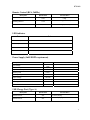
1-1 Location of PCB Boards
1-2 Versions Variation & PCBA Repair Policy
Type/Versions
Board in used
BTS3000G
/10
Mainboard
MLR
AMP board
MLR
Vol. board
MLR
Remark:
CLR = Component Level Repair
MLR = Module Level Repair
2
BTS3000
2
Specification
General
Model Name:
BTS3000 connected audio speaker
Main features:
1. Audio source: AUX IN/Bluetooth/Coaxial/Optical
Bluetooth with APT-X decoder, Coaxial, Optical support PCM format only
2. Audio output power: 2X10W at THD 10%
Bass driver: 4 inch, Tweeter: 0.75 inch.
3. USB port provides 2A(max) charge current
Key parts:
1. Bluetooth module: BM845 ROM, CSR chipset
2. Coaxial/Optical IC: CS8422-CNZ QFN32
3. Audio power amp.: BT4860B
4. DAC IC: CS4354
5. MCU IC: SSI95F165AQPP
Lifetime :
3 years
Safety requirements
IEC60950-1, EN60950-1. For details refer to approbation plan.
EMC requirements
Active Radiation, Radiation Immunity, Conductive Interference ( R&TTE ,FCC ID,IC ID )
EN 300 328, EN 55022/EN 55024, EN 301 489-1/-17, EN 50385, IC RSS 210,
IC RSS 102
For details refer to approbation plan.
Climatic requirements( indoor product/ all climates , not water/rain resistant)
Operating Temperature: 0°C to +40°C, Humidity: 8% to 90%.
Storage Temperature: -25°C to +60°C, Humidity: 5% to 90%
Power supply
AC 100V—240V , 36W
Weight:
4.1 Kg ±5% (with accessories)
3
BTS3000
Audio Specification
1. Coaxial and Optical
Test Conditions
a) Speaker output load: 2* 6, b) Input PCM audio signal from coaxial/ optical sources.
Standard: IEC60958-3, TOSLINK
Limi
Item
Condition
Norm.
Unit
Remark
SN
t
20Hz+/Output Power
W
20kHz
1
10W
Load 6 L/R
10%
At 10% THD
LPF
Operating Temperature
SNR (A-weighted)
0-40
Input 1kHz
70
65
Input 100—
16KHz
70
65
10020KHZ
Frequency response
Left-Right Channel
Separation
Left-Right Channel Balance
℃
2
dB
3
Hz
Left-Right
45
Right-Left
45
Input 1kHz
1
dB
Input 100—
16KHz
1
dB
dB
Hum noise
Left/Right (W/A)
<3.0
+/-3dB
frequenc
y
mV
4
5
6
20Hz20kHz
LPF
7
4
BTS3000
2. AUX IN
Test Conditions
b) Speaker output load: 2* 6
Item
Output Power
At 10% THD
Condition
Load 6 L/R
Operating Temperature
Norm.
Limi
t
10W
+/10%
0-40
Input 1kHz
70
10020KHZ
Frequency response
Left-Right Channel
Separation
Left-Right Channel Balance
70
Left-Right
Remark
SN
W
20Hz20kHz
LPF
1
℃
2
dB
3
65
SNR (A-weighted)
Input 100—
16KHz
Unit
65
Hz
+/-3dB
frequenc
y
45
dB
Right-Left
45
Input 1kHz
1
Input 100—
16KHz
4
5
dB
6
1
dB
Hum noise
Left/Right (W/A)
<3.0
mV
Left at 10%THD
1000
mVrm
s
1000
mVrm
s
20Hz20kHz
LPF
7
8
Sensitivity
Right at 10%THD
5
BTS3000
3. Bluetooth streaming
Test Conditions
c) Speaker output load: 2* 6, b) Streaming audio signal from iPhone 4/iPad2
Item
Condition
Norm.
Limi
t
Unit
Remark
SN
Output Power
At 10% THD
Load 6 L/R
10W
+/10%
W
20Hz20kHz
LPF
1
Operating Temperature
0-40
Input 1kHz
70
10016KHZ
Frequency response
Left-Right Channel
Separation
Left-Right Channel Balance
Hum noise
70
Left-Right
2
dB
3
65
SNR (A-weighted)
Input 100—
16KHz
℃
65
Hz
+/-3dB
frequenc
y
4
45
dB
Right-Left
45
Input 1kHz
1
5
dB
6
Input 100—
16KHz
1
dB
Left/Right (W/A)
<3.0
mV
20Hz20kHz
LPF
7
Bluetooth Distance
Description
Reception Distance( free field)
Frequency range
Specification
Test Condition
>10m
Streaming music smoothly
2.4GHz—2.5GHz
6
BTS3000
Remote Control (RC6, 36KHz)
Description
Operating distance
Specification
Test Condition
>10m
0 deg.
30 deg. (hor. & vert.)
>7.92
45 deg. (horizontal)
>5,65
LED indicator
Source
Color
Power/BT white
Optical white
Coaxial white Aux‐in/RCA white Power Supply (fulfil ERP2 requirement)
Description
Input Voltage
Over current protection
Specification
AC 100v to
240v
Yes(3.5A)
Output short circuit protection
Test Condition
Yes
Efficiency level
Level v
Operating Temperature
0~40
Output Voltage
DC 12V
Output Current
3A
Line Length
1.5m
Connector
IEC
USB Charge Port (Type A)
Description
Specification
OUTPUT DC 5V
≤2A
OUTPUT DC 5V
≤1A
Test Condition
no music playing
With music playing
7
BTS3000
ESD
Test Method: EN61000-4-2
• Ambient temperature : 15 – 35 °C
• Humidity: 30 – 50%
• Pre-condition for the set before test : put the set into the ESD room at least 4 hours
• Supply: AC
• Set condition: Audio mode
Test requirement:
• Contact discharge : from 0 kV to ± 8 kV
• Air discharge : from 0 kV to ± 15 kV
Severity level
Contact discharge (+/- kV)
Air discharge (+/- kV)
Small pop noise
Large pop noise
Short mute (<1 second)
Long mute (>1 second)
Short wrong display (<1 second)
Long wrong display (>1 second)
Change of function – recover by
normal intervention
Loss of volatile memory
Reset
Shut down – recover by on-off button
Hang up – recover by play/onoff/reset button
Hang up – recover by re-connect
power
Go to record mode
Go from standby to on mode
Loss of fixed stored data
Component damaged
Note: X = not allowed, P = allowed.
1
0-2
0-4
X
X
X
X
X
X
2
2-4
4-8
P
X
P
X
P
X
3
4-5
8-10
P
P
P
P
P
P
4
5-7
10-15
P
P
P
P
P
P
5
N.A.
N.A.
P
P
P
P
P
P
X
X
P
P
P
X
X
X
X
X
X
P
P
P
P
P
P
P
P
P
X
X
P
P
P
X
X
P
P
P
X
X
X
X
X
X
X
X
P
P
X
X
P
P
X
X
P
P
X
X
S/N
8
BTS3000
Mechanical Specification
Item
Limit
Remarks
Drop Test:
Limit
Remarks
NA
Criteria: set has no
functional damage & major
cosmetic defect after test.
70cm Face drop /
35cm Edge&Corner
drops
70cm Face drop /
35cm Edge&Corner
drops
Criteria: set has no
functional damage & major
cosmetic defect after test.
Criteria: set has no
functional damage & major
cosmetic defect after test.
Bare Drop (w/o packing)
Normal Drop with full package
Cold Drop with full package
Mechanical miscellaneous
No sharp point on the unit accessible by end user is allowed.
Rattle is not allowed on the desktop usage.
Cosmetic Specification
Part
scratch
Defects of dirt-mark, dust particle, hole, rough part, should be
Gap
Limit
Remarks
less than 0.3mm
≤0.3mm
9
BTS3000
3
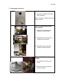
Disassembly Instruction
Open the speaker
1) Unscrew 13 screws at the back
side of speaker
Note: 2 screws on power cord socket
does not need
Rmove the AMP board module
from speaker
1) Unplug two connectors from
sockets on volume board
2) Unplug these connectors from
sockets at top view side
3) Unplug these connects from
sockets on right hand side
Remove the Main board from
speaker
1) Unscrew the vol. and source
button
2) Disconnect these sockets as
circled on picutre
10
BTS3000
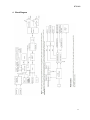
4
Block Diagram
11
5-1
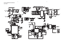
5-1
CIRCUIT DIAGRAM - AMP BOARD
PART 1
D12
1 VDD_SMPS
C2
103/1KV
1
2
SMPS
D3
Q2
R50
0603
47K
220uF/16V
R7
5%
PGND
C4
5%
1
R13
1
2
1000uF
25V
25V
0603
VCC
0805
9.1K
2.2K
0805
R17
5%
1
R
GATE
GND
4
VDD
FB
2
R8
224
C10
1
2
A 3
K
TL431
BPC817A
R18
5%
8
7
10K
1%
1
2
NC
6
5%
C88
103
25V
0603
C6 0805
104 50V
PGND
104
50V
0805
VCC12V
[3]
R15
12 12
VCC_U7
[2]
5%
R27
5
U7-B
8
+
G V
REF
0603
47K
4
6
[2]
7
KS4558
LOUT+
15 15
LOUT14 14
C31
220uF/16V
2.2
0603
2.2
0603
R95
5%
R92
5%
5%
R93
0603
2.2
[3]
5%
R94
224
0603
50V
33pF
C39
9
FB1
6
0603
20K
5%
R26
5%
R49
0603
68K
[3]
0603
2.2
0603
10V
C47
4.7uF
10V
0603
7.5K
0603
S-GND
11 11
+
5%
R53
R54
5%
C20
4.7uF
33pF
C34
0603
47K
0603
50V
C55
50V
33pF
C40
1
50V
0603
C18
100pF
5%
R4
ROUT2 2
10uF
KS4558
0603
1K
470 ohm
LOUT+
BT4860B
-
3
[2] FB3
C81
104
0603
25V
C80
104
C84
104
25V
0603
104
C83
25V
0603
25V
0603
LOUT-
VCC_U7
5%
R74
0603
50V
33pF
C56
GND
[2]
0603
20K
R73
5%
GND
5%
R59
[2]
1
2
C52
20K
0603
5 5
8
REF
0603
47K
ROUT+
1 1
VCC_ST
SVR
[2]
Right Satellite
JP3
U7-A
2
104
C85
V+2
V+1
1/16W 5%
ST-BY
7.5K
0603
5%
R58
224 0603
FB2
0603
25V
3
13
7
0603
22K
10V
0603
C57
4.7uF
50V
0603
0603
20K
2
R57
5%
0603
68K
5%
R48
1
33pF
C114
10V
0603
&21B7+B3B00B/)
POWER_EN
&1
[2]
C17
4.7uF
0603
50V
C50
100pF
5%
R55
VCC
[2]
5%
R98
2.2K
5%
R21
0603
1K
0603
47K
10V
0603
C62
4.7uF
CATHODE
0805
U1
100K
0805
R9
4 4
10V
0603
1
2
3
4
5
OUTPUT
47uF
16V
10uF
25V
C60
4.7uF
EMITTER
SMPS
ANODE
C26
5.0V
[3]
C41
C27
L
COLLECTOR
3
220
L8050HT1G
STANDBY
R
0.68/1W
U2
1
3
VCC_ST
GND
INPUT
[2]
2
102/400V
6)
NC
2
0603
47K
3
L8550HLT1G
C9
102
C30
1
78L05
Q3
2
5%
3
1
5%
R5
C21
R12
100
0805
U3
U6
2
0603
25V
5%
R45
1
R33
POWER_EN
2
0603
5%
[2]
0603
1K
102
C24
R46
POWER PLUG
ACIN 230V
4.7K
R32
1
5%
104
C25
22uF/50V
VCC
R6
5%
SENSE
[2]
0805
50V
RI
0805
50V
C5
102/1KV
100uH
CY2
VCC
C23
0805
100
L3
VCC12.8.V
C8
104
ER25-001
FR104
0805
2
4.7
[2]
1
2
C3
101/1KV
560K
0805
VCC
S
C42
102/1KV
100
0805
1N4007
1
D6
G
R2
5%
CN4
CON_TH_2P_2.54MM
1
R11
5%
[2]
1
2
560K
0805
D4
CN6
CON_TH_2P_2.54MM
D
5N60
102/1KV
L1
1000uF
25V
Q1
C71
R1
5%
1
2
AC_JACK
1
50V
0805
C19
SR5100
D8
1
1N4007
C7
3
;PP
T2.0AL/250V
104
SR5100
D7
TR1
0805
NP
4
4
2
102/400V
10*6*5MM 0.6MM
1
1
2
D5
33uF/400V
UU9.8
CY1
FR107
2
3
1
MOV1
14D471K
LF1
1%
R20
FUSE
1
2.2K
0805
56K/1W
50V
0805
R25
5%
0.1uF/275V
1
CX1
R3
2
C1
1N4007
2
D2
R23
5%
1
2
1
2
2M
R22
0805 5%
2M R24
0805 5%
CON1
CN
2M
0805
2M
0805
1N4007
10uF
GND
0603
50V
33pF
C54
REF
2200uF
25V
5-2
5-2
CIRCUIT DIAGRAM - AMP BOARD
PART 2
4
F6
FB1K
R200
3
FB1K
2
5
2
GND
OPITCAL
C32
1
C33
*1'
23,7&$/
1
16V
102
9
4
VOUT
0603
16V
10%
JK3
104
0603
3
VCC
&2$;
ESD
GND
ESD3
5V_CHARGE
[1,2]
1
2
2
[3]
3
4
1
20MH
L14
F5
ESD
ESD2
FB1K
&1
F7
10R
&1
ESD
5V
C101
10uF
AUXR
6.3V
0805
GND
AUXL
5
F8
FB1K
[2]
4
F1
FB1K
[2]
3
F4
FB1K
2
F3
FB1K
1
F2
FB1K
STANDBY
C11
5.0V
3
FB1K
R99
1%
5
ESD1
STANDBY
R101 1%
49.9K 0603
75
ESD
5V_CHARGE
F9
6
[3]
0603
1%
0603
49.9K
CN3
LOUT+
LOUT-
[2]
[2]
R6H6
L2
L4
R6H6
COAX
GND
AUXR
-.
IR1
IR
CN2
9
*1'
,5
1
ESD
R112
2
I
G
O
5
GND
0603
NC
1
2
3
4
GND
POWER
DATADATA+
43.2K
JK4
1% 75K
R100 0603
R102
R28
ESD4
3
D9
ESD
C68
C69
8
ESD
ESD9 ESD8
ESD
ESD7
5-3
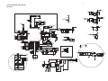
5-3
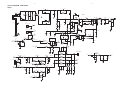
CIRCUIT DIAGRAM - MAIN BOARD
audio PART
&1
'9&&
>@
&
5
&
.
9
9''
*1'
9%$7
5
)1
.
>@
32:(5B&21752/
. 5
.
5
&
5;3
9'B),/7
5;1
9B5(*
6$2)
7;8
06B6(/
&
&
5
5
&/.
9&&
8
1&
1&
%
(
4
&
)/<3
/5&.
9$
6&/.'(0
*1'
*1'
$287%
),/7
$287$
&
&
&
8
)%.
5
&
&
&
.
5
&
&
8
5
)%.
&
>@
.
5
.
5
)%.
8
&
0&/.
23&2$;B6(/
.
>@
5
.
&
&
)/<1
>@
39
>@
&2;/
&
)%.
&(
8
.
.
1&
5
&
9),/7
5
&
5
1&
.
%79
&(
5
8
.
1&
9/
6',1
5
5
2/.
7'0B,1
6'287
26&/.
'*1'
5;B6(/
5&%/
.
8
&6
$*1'
7;B6(/
5
5
&
5
&
1&
9/
>@
&
23B,1
8
26&/.
6'287
9$
0&/.B287
5;12
;72
5;3
2/5&.
&
65&B81/2&.
3,2
5
&
5
>@
.
5
;7,
>@
5
567
.
.
50&.
>@
.
5
5
5
5
5
5
)1
.
&6
8
>@
&
)%.
.
<
5
&
5
&
>@
>@
5
5
3,2
9%$7B6(16(
&+*B(;7
9%86
>@
>@
5
)%.
3,2
3,2>@
1&
.
5
9$8',2
3,2
.
5
&
5
5
195(55
3,2>@
5 5
.
087(
.
5
.
5
.
3,2
*1'
&
3
3,2
3,2>@
*1'
&
3
0,&B51
0,&B53
0,&B/1
$*1'
0,&B/3
63.B51
63.B53
*1'
3,2>@
5
.
%7B5
5
5
5&+
.
>@
39
>@
1&
&
>@
B$
$8;B5
&
.
39
.
&
&
&
&
63.B/1
63.B/3
*1'
*1'
/('
5)
86%B1
3,2>@
3,2>@
86%B3
>@
>@
8
8
8
8
3,2
3,2>@
95(*(1$%/(
3,2
%0
%0
63,B3&0
>@
)%.
&2$;B,1
3,2
/
3,2>@
567
)%.
>@
&
3,2
3,2>@
/
63',)B567
3,2>@
3,2>@
.
67$1'%<
5
5
3,2>@
B%
5
4
&
>@
&
)%.
>@
>@
$,2>@
63,B026,
63,B&6%
63,B&/.
63,B0,62
*1'
9
*1'
39
/
>@
5
5
8
% 5
&
*1'
/('
/('
5,1
$8;B/
1&
&
,&B6'$
5
.
$8;B5
>@
&
.
$ 8
.
5
.
.
5
5
.
8%
NV
5
5
5
5
.
.
&
.
$8;B/
67$'%<
.
5
.
0,&B%,$6 *1'
/('
3,2
/('
&
/&+
4
5
8
37
8
1&
%7B/
S
5B'(7
,1+
>@
*1'
8$
NV
>@
1&
3
*1'
5287 5
/,1
.
&(
! " #
&1
1&
&
/B'(7
8
5
&
3
&
>@
5,1
.
&
S
&1
8
&
&
&
/287 /,1
&
3
1&
&
&
5,1
5,1
8
&
>@
$8;B5
5
( 4
&
5
%
&
.
.
3
&
8
$17
8
>@
,&B6&/
.
/,1
&
39
5B'(7
8
&
>@
$8;B/
39
&
.
&
&
5
.
)%.>@
5
3
>@
%7B5
5
.
>@
>@
.
5
5
.
3
&
%7B/
3,1 62&.(7
&1
5
.
39
8
2/,1
5
'$7$
8
&
>@
&2;5
+&
,1
>@
&2;/
8
*1'
/ 0+
&
>@
>@
&
8
&
8
&
&
5
.
(
4
&
9&&
&
9,1
0
'
8
&
*1'
( 4
&
3,1 62&.(7
&1
5
9287
%
%
*1'
5
&
.
5
32:(5B(1
>@
5
9287
.
>@
5
8
&
9((
)%.
8
&
)%.
>@
9,1
9&&
&
&
8
/B'(7
&
&
5
.
&
>@
(53
/
39
>@
5&+
)%.
>@
32:(5B(1
/
9&& &
3
3
/&+
.
.
.
.
.
.
&
'
&
5&+
,1
5
.
5
.
5
>@
$*1'
5
.
5
.
/&+
39
5
5
5
5
5
5
>@
&
>@
39
.
5
&2;5
5-4
5-4
CIRCUIT DIAGRAM - MAIN BOARD
MCU PART
)%.
/
>@
9
,1 9287
5
5
>@
%/8(/('
.
%3
(1
5
&
&
8
*1'
.
&
/
)%.
9B0&8
5
>@
>@
5
.
3>@BB$'
7;
&
+6&/BBB3>@B'$
.
5
>@
>@
>@
.
5
.
5
.
5
.
5
>@
3>@B'$
>@
,&B6&/
,&B6'$
>@
(6'
'
$
>@
(
&
%
&2$;B,1
'
23B,1
>@
/
39
*1'
.
3
&
8
&
5
,1
%67
'
&
X+$
/
&
6:
(1
3
&(
5
736
8
&
8
5
.
5
.
%227
3+
9,1
*1'
(1
&203
66
66
9&&
'
&
>@
& & &
.
9616
5
.
&
5
8
&
&
8+
>@
/
&
*1'
&1
>@
)%
5
1&
1&
5
.
&
3
5
.
&(
8 /(65
/ 0+
9
*1'
&1
&
8
03
.
.
5
&(
'9&&
.
&
8
23,7&$/
5
&
/('
*1'
)%.
.
&
EOXH/('
&
3$'
3
&2$;
>@
%/8(/('
32:(5B(1
&
/('
/
9B0&8
3
3$'
9
8
5
$8;/('
>@
>@
>@
$8; /('
&2$;/('
3
3$'
(1
5
23/('
>@
$ $ $ 966 5
9B0&8
&
/('
&2$; /('
>@
9&&
:3
6&/
6'$
6285&( 32:(5&/($5
&
>@
/&6
8
23&2$;B6(/
>@
5
(6'
'
)%.
23 /('
&
1&
9B0&8
5
&
*
&
'
(6'
/('
&
.
>@
5
4
.
>@
5
9B0&8
5
.
.
>@
63',)B567
5
5
.
.
5
32:(5B(1
$8;/('
>@
.
>@
.
5
&2$;/('
>@
5
.
.
&
/('
5
92/80(
5
8 /(65
&
&
&(
/('
5
.
(1
8
&
5
5
.
.
*1'
32:(5B&21752/
.
5
.
3
%
9B0&8
3,2
9''
3>@BB$
.
5;
.
9B0&8
3
(6'
'
>@
>@
3>@B$
3>@BB'$
+6'$BB3>@BB'$
3>@B$
3>@BBB'$
3>@BB'$
3>@BB&/.2
3>@BB(7
3>@BB$
3>@BB$'
3>@BB$
5
3>@B$
.
3>@B$
5
&
5
&
5
>@
3
567
.
&
(
'
5
&
7;
3$' 5;
39
5
3$'
>@
,5
+6&/BB3>@BB5;'
.
$
&
&1
23/('
3>@BB$
>@
5
(6'
'
>@
($
3>@BB,17
+6'$BB3>@BB7;'
66,)$433
5
3>@BB$'
5
.
3>@BB,17
*1'
3>@BB:5
3>@BB5'
;
;
966
3>@BB$'
3>@BB$
3>@BB$
8
9
%/8(/('B(1
.
)1
$/(
8
5
.
)1
>@
/
>@
5
.
.
B%
>@
>@
.
B$
5
5
5
5
9B0&8
%3
%7
9B0&8
>@
'
)%.
&
(1
6
5
*1'
&
36(1&/.2
*1'
,6'$BB3>@B7
3>@BB$
3
&
8
&
*1'
3
&
3
.
,6&/BB3>@B7
3>@B$
&
.
3>@B$
5
5
,1 9287
%79
39
&
3>@BB$
.
3>@BB$
>@
3>@B$
5
<
0+]
5
5
5
5
,&B6'$
.
.
,&B6&/
5
&
&(
(53
>@
.
8
3
.
9B0&8
>@
>@
.
.
.
>@
.
>@
>@
>@
57B9
8
%/8(/('B(1
,1
>@
39
4
>@
087(
9
67$1'%<
&
/
5
5
P+
1&
9B0&8
57B9
8
&
.
>@
>@
9
5-5
5-5
CIRCUIT DIAGRAM - VOLUME BOARD
R47
5%
C51
2.2nF
R62
5%
3
100nF
C29
VR2-A
100K
R42
5%
1
0603
16V
100K
1
220nF
C36
C43
0603
25V
CN7
1
10nF
3
3
0603
1.5K
2
4
5%
R30
4
R61
5%
4
4.7K
0603
0603
10K
0603
16V
220nF
C35
R37
5%
R40
5%
VR2-B
5
VR1-B
NC
0603
5
100K
100nF
C48
100K
6
5%
R60
0603
25V
R39
5%
50V
0603
0603
4.7K
50V
0603
C37
2.2nF
5%
R41
C16
33pF
5%
R43
POW
CN8
0603
4.7K
R
680
0603
2
6
G
R36
5%
4
L
10K
0603
2
2
VR1-A
NC
0603
4.7K
0603
3
R38
5%
0603
25V
1
4.7K
0603
50V
0603
0603
4.7K
50V
0603
R44
5%
5%
R35
C22
33pF
1K/100M
0603
C38
10nF
680
0603
R34
1.5K
5%
0603
25V
0603
1K/100M
0603
L
G
R
POW
5-6
CIRCUIT DIAGRAM - MAIN BOARD
5-6
BTS3000
6
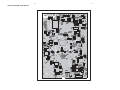
Mechanical Exploded View
Right Speaker
Left Speaker
18
BTS3000
7
Revision List
2013-11-28 V1.0 Initial release
19