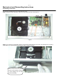
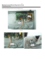
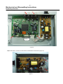
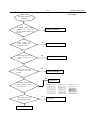
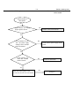
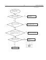
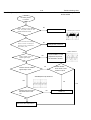
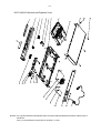
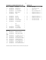
1
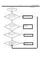
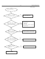
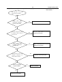
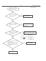
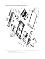
DVD Player
DVP3140,DVP3142(K)
DVP3140/37
DVP3142/12/51/55
DVP3142K/55
Service
Service Manual
TABLE OF CONTENTS
Page
. Technical Specifications……………………………………..............1-2
. Safety Instruction, Warning & Notes….……………………....…..... 1-3
.
. Mechanical and Dismantling Instructions…………........................2-1
. Region Code, Software Version& Upgrades…………….................3-1
. Trouble Shooting Chart………………………………………………..4-1
. Wiring Diagram………………………………………..………..….….,5-1
. Electrical Diagrams and Print-layouts..….…………………....….….6-1
. Set Mechanical Exploded view..................…………………..….….. 7-1
.
. Revision List…..........………………………………………..…..….....8-1
©Copyright 2007 Philips Consumer Electronics B.V. Eindhoven, The Netherlands
All rights reserved. No part of this publication may be reproduced, stored in aretrieval system or
transmitted, in any form or by any means, electronic, mechanical, photocopying,
CLASS 1
LASER PRODUCT
or otherwise
without the prior permission of Philips.
Published by TCL-HY 0701 Service Audio
Version 1.0
Printed in The Netherlands
Subject to modification
GB
3139 785 32450
PHILIPS
1-2
Technical Specifications
TV standard
(PAL/50Hz)
Number of lines
Playback
(NTSC/60Hz)
625
Multi standard
525
(PAL/NTSC)
Audio performance
DA converter
DVD
SVCD
Video performance
Video DAC
YPbPr:
Video output
12 bit, 108MHz
0.7Vpp ---- 75 ohm
1Vpp ----- 75 ohm
RGB(SCART)
0.7Vpp ---- 75 ohm
24bits, 192KHz
fs 96kHz
fs 48kHz
fs 48kHz
fs 44.1kHz
fs 44.1kHz
CD/ VCD
Signal-Noise (1kHz)
Dynamic Range (1kHz)
Cross talk (1kHz)
Distortion/Noise (1kHz)
MPEG MP3
4Hz----44kHz
4Hz----22kHz
4Hz----22kHz
4Hz----20kHz
4Hz----20kHz
>90dB
>80dB
>70dB
>65dB
MPEG Audio L3
Video format
Digital Compression
X
MPEG 2 for DVD,SVCD
MPEG 1 for VCD
Div ®
DVD
Horiz resolution
Vertical resolution
50Hz
720 pixels
576lines
60Hz
720 pixels
480 lines
VCD
Horiz. resolution
Vertical resolution
50Hz
352 pixels
288lines
60Hz
352 pixels
240 lines
Connections
Scart Oupput
YpbPr output
Video output
Audio output (L+R )
Digital output
Cabinet
Dimensions (w X h X d)
Weight
MPEG/AC-3/
PCM
MP3(ISO 9660)
360 x 38 x 209 mm
360 x 37 x 209 mm (Only for DVP3142K/XX)
Audio format
Digital
Euroconnector
Cinch 3x
Cinch( yellow)
Cinch (white/red)
1 coaxial
IEC60958 for CDDA/ LPCM
IEC61937 for MPEG1/2,
Dolby Digital
Compressed
Digital
16, 20, 24bits
fs, 44.1, 48, 96KHz
96,112,128,256kbps
& variable bit rate fs,32,
44.1,48 kHz
Analogue Sound Stereo
Dolby surround compatible downmix from Dolby Digital multi-channel
sound
Approximately 1.35 kg
Power consumption
Power supply Rating
Power consumption
Power consumption in standby mode
110V-240V;
50/60HZ
<10W
<1W
Specifications subject to change without prior notice.
1-3
Safety instruction, Warning & Notes
Safety instruction
2.Laser safety
1. General safety
This unit employs a laser. Only qualified service personnel
Safety regulations require that during a repair:
. Connect the unit to the mains via an isolation transformer.
. Replace safety components indicated by the symbol
,
only by components identical to the original ones. Any
other component substitution (other than original type)
may increase risk of fire or electrical shock hazard.
may remove the cover, or attempt to service this device
(due to possible eye injury).
Laser device unit
Type
: Semiconductor laser GaAlAs
Wavelength
: 650nm (DVD)
: 780nm (VCD/CD)
Safety regulations require that after a repair, you must
Output power
: 10mW (DVD /CD)
return the unit in its original condition. Pay, in particular,
Beam divergence: 60 degree
attention to the following points:
. Route the wires/cables correctly, and fix them with the
. Check the insulation of the mains lead for external
hazardous radiation exposure. Avoid direct exposure to
beam.
damage.
. Check the electrical DC resistance between the mains
plug and the secondary side:
1) Unplug the mains cord, and connect a wire between
the two pins of the mains plug.
2) Set the mains switch the “on” position (keep the
mains cord unplug).
3) Measure the resistance value between the mains
plug and the front panel, controls, and chassis
bottom.
Repair
Note: Use of controls or adjustments or performance of
procedure other than those specified herein, may result in
mounted cable clamps.
4)
or
correct
: 7mW (DVD)
unit
when
Ω .
measurement is less than 1M
the
resistance
5) Verify this, before you return the unit to the
customer/user (ref. UL-standard no. 1492).
6) Switch the unit “off”, and remove the wire between
the two pins of the mains plug.
1-4
Warning
1.General
2. Laser
. All ICs and many other semiconductors are susceptible to
. The use of optical instruments with this product, will
electrostatic discharges (ESD). Careless handing during
increase eye hazard.
repair can reduce life drastically. Make sure that, during
. Only qualified service personnel may remove the cover
repair, you are at the same potential as the mass of the
or attempt to service this device, due to possible eye
set by a wristband with resistance. Keep components and
injury.
tools at this same potential. Available ESD protection
with a disc loaded inside the player.
equipment:
1)
. Repair handing should take place as much as possible
Complete kit ESD3 (small tablemat, wristband,
connection box, extension cable and earth cable)
. Text below is placed inside the unit, on the laser cover
shield:
4822 310 10671.
2)
Wristband tester 4822 344 13999.
. Be careful during measurements in the live voltage
section. The primary side of the power supply , including
the heat sink, carries live mains voltage when you
CAUTION: VISIBLE AND INVISIBLE LASER
RADIATION WHEN OPEN, AVOID EXPOSURE
TO BEAM.
connect the player to the mains (even when the player is
“off”!). It is possible to touch copper tracks and/or
components in this unshielded primary area, when you
Notes:
service
Laboratories. The double-D symbol is trademarks of Dolby
the
player.
Service
personnel
must
take
precautions to prevent touching this area or components
in this area. A “lighting stroke” and a stripe-marked
printing on the printed wiring board, indicate the primary
side of the power supply.
. Never replace modules, or components, while the unit is
“on”.
Manufactured
under
licence
Laboratories, Inc. All rights reserved.
from
Dolby
1-5
Notes
Lead-Free requirement for service
INDENTIFICATION:
•
Regardless of special logo (not always indicated)
Use only original spare-parts listed in the
Service-Manuals. Not listed standard-material
(commodities) has to be purchased at external
One must treat all sets from 1.1.2005 onwards, according
next rules.
companies.
•
Important note: In fact also products a little older can also
be treated in this way as long as you avoid mixing
solder-alloys (leaded/ lead-free). So best to always use
SAC305 and the higher temperatures belong to this.
Special information for BGA-ICs:
- always use the 12nc-recognizable soldering
temperature profile of the specific BGA (for
de-soldering
always
use
highest
lead-free
temperature profile, in case of doubt)
Due to lead-free technology some rules have to be
respected by the workshop during a repair:
- lead free BGA-ICs will be delivered in so-called
• Use only lead-free solder alloy Philips SAC305 with
‘dry-packaging’ (sealed pack including a silica gel
order code 0622 149 00106. If lead-free solder-paste is
pack) to protect the IC against moisture. After
required, please contact the manufacturer of your
opening, dependent of MSL-level seen on
solder-equipment. In general use of solder-paste within
indicator-label in the bag, the BGA-IC possibly
workshops should be avoided because paste is not easy
still
to store and to handle.
communicated via AYS-website.
to
be
baked
dry.
This
will
be
Do not re-use BGAs at all.
• Use only adequate solder tools applicable for lead-free
solder alloy. The solder tool must be able
has
•
For sets produced before 1.1.2005, containing
o To reach at least a solder-temperature of 400°C,
leaded soldering-tin and components, all needed
o To stabilize the adjusted temperature at the
spare-parts will be available till the end of the
solder-tip
o To exchange solder-tips for different applications.
• Adjust your solder tool so that a temperature around
360°C – 380°C is reached and stabilized at the solder
joint. Heating-time of the solder-joint should not exceed
service-period. For repair of such sets nothing
changes.
• On our website:
www.atyourservice.ce.Philips.com
You find more information to:
~ 4 sec. Avoid temperatures above 400°C otherwise
BGA-de-/soldering (+ baking instructions)
wear-out of tips will rise drastically and flux-fluid will be
Heating-profiles of BGAs and other ICs used in
destroyed. To avoid wear-out of tips switch off un-used
Philips-sets
equipment, or reduce heat.
• Mix of lead-free solder alloy / parts with leaded solder
You will find this and more technical information
alloy / parts is possible but PHILIPS recommends
within the “magazine”, chapter “workshop news”.
strongly to avoid mixed
For additional questions please contact your local
solder alloy types (leaded and lead-free). If one cannot
repair-helpdesk.
avoid, clean carefully the
solder-joint from old solder alloy and re-solder with new
solder alloy (SAC305).
2-1
Mechanical and Dismantling Instructions
Dismantling Instruction
The following guidelines show how to dismantle the player.
Step1: Remove 5 screws around the Top Cover, then remove the Top Cover (Figure 1).
Figure 1
Step2: If it is necessary to dismantle Loader or Front Panel, It should be remove the Front door assembly first. (Figure 2)
Note: Make sure to operate gently otherwise the guider would be damaged.
Please kindly note that dismantle
the front door assembly carefully
to avoid damage tray and the
front door assembly.
Figure 2
2-2
Mechanical and Dismantling Instructions
Dismantling Instruction
Step3: If the tray can’t open in normal way, you can make it through the instruction as below (Figure 3).
Note: Make sure to operate gently otherwise the guider would be damaged.
Push the guider until the tray out.
Make sure to operate gently to
avoid damage happening.
Figure 3
Step4: Dismantling Loader, disconnect the 3 connectors aiming in the below figure, and remove 1 screw at the
bottom of Loader. (Figure 4)
CON 1
CON 2
CON 3
Figure 4
2-3
Mechanical and Dismantling Instructions
Dismantling Instruction
Step5: Dismantling Front Panel, disconnect the 1 connector, then release the snaps on the both sides of Front Panel and bottom
cabinet , then gently pull the Panel out from the set. (Figure 5 & 6 & 7)
CON 5
CON 4
Figure 5
Snap 1
Snap 2
Figure 6
Figure 7
2-4
Mechanical and Dismantling Instructions
Dismantling Instruction
Step6: Dismantling Main Board, first disconnect the connector, and then remove 4 screws. (Figure 8)
CON 6
Figure 8
Step7: Remove the 2 screws on Power Board to dismantle the Power Board. (Figure 9)
Figure 9
3-1
Software upgrade
Preparation to upgrade software
B. Read out the software versions to confirm upgrading
1)
Start the CD Burning software and create a new CD
1)
project (Data Disc) with the following setting:
2)
Label: DVP3XXX
(No need the label name)
Note: It is required capital letter for the File System
2)
Power up the set and open the tray door.
Press <9><6><6> button to check the software
information.
The software version and other information are display
name, and it no need have the File name during
on the TV screen as follows:
start the CD burning software for Zoran project.
BE Version: DVP3XXXXX_XX.XX
Burn the data onto a blank CDR
FE Version: DCX.XXXXXX.XX.XX
DSP Version: DSP.XX
Region Code: X
A.
Procedure for software upgrade:
1) Power up the set and insert the prepared Upgrade
CDR.
2) The set will start reading disc & response with the
following display TV screen:
Loading
Firmware Upgrade Erase and program.
Start
Cancel
Select Start to start upgrade.
3) Press <OK> button to confirm, then screen will display :
Firmware Upgrade Programming, Please Wait...
Do not Switch the Player Off !
4) The upgraded disc will automatically out when files
coping complete, then take out the disc.
5)
About 1 minute later, the trace will automatically close
when upgrading complete.
Caution: The set must not be power off during
upgrading, Otherwise the Main board will be
damaged entirely.
4-1
Trouble shooting chart
Remark: Trouble shooting chart for
DVP3140/XX
Spindle motor does not move
Motor no move
Go
Check the FFC connection
No
Correct connection
between 24P and the loader.
Yes
No
Check whether “RFA5V”
Check
(+5V) voltage is normal.
the
RFA5V
power
supply
Yes
Check whether laser voltage
No
(2.3V for DVD & 1.9V for CD)
Check/Replace Q2、Q3.
on Collector of Q2 and Q3
Yes
1.Whether voltage on pin 129 of U1
No
varies between 0 and 3.3V (3.3V for
CD and 0V for DVD),
Check/ Replace U1.
2.Whether peripheral components
are eroded or badly soldered.
Yes
1.
Have no
focus
No
Check
U1
182pin
FOCUS_PWM signals
2.If there are F+, F-, T+ and Tsignals output from U7.
Yes
FOCUS_PWN waveform
Check/Replace the loader
4-2
Trouble shooting chart
Remark: Trouble shooting chart for
DVP3140/XX
The power can not be on or off
The power can’t be
on or off
Go
Check the power supply
No
on the power board is
Repair the power board
normal.
Yes
Check if the CON301 on
the front board to CN5 on
Yes
No
Check/Correct
connection
the decoder board is in
good contact.
Yes
Whether the connection
No
to K301 is broken.
Correct the connection
Yes
Whether there is 0V and
3.3V voltage difference on
Pin 94 PCON of U1.
Yes
No
Replace U1.
4-3
All output voltages on the power board is 0V or deviated.
Trouble shooting chart
Remark: Trouble shooting chart for
DVP3140/XX
All output voltages on
the power board is 0V or
deviated
Yes
Check whether
Yes
Replace F1
F1 is blown
No
Check whether there is
No
Replace C1&C2 if D1, D2, D3, D4 are
normal.
300V on C1 and C2.
Yes
Check whether 100KHz
oscillating signal on
Pin6 of U1
No
Check/ replace U1.
U1(PIN 3 - RC waveform)
U1(PIN 8 - Drain waveform)
Yes
Check if +5V, , +12V and -12V
are short.
Yes
Check whether the components in the
short-circuit voltage are defected or eroded.
No
Check whether U1 are eroded.
4-4
Trouble shooting chart
Remark: Trouble shooting chart for
DVP3140/XX
Disc cannot be read.
Disc cannot be read.
Yes
No
Check the FFC connection
Check the loaded circuit
between 24P and the loader.
Yes
1.Check voltage on pin 100 of U1 varies
Check whether there is laser
No
voltage (2.3V for DVD and 1.9V
between 0 and 3.3V:
Æ3.3V for CD
Æ0V for DVD
for CD) on Collector of Q2 &Q3
2.Check whether peripheral components
are eroded or defect
Yes
Check
U1,
U7,
and
No
Re-solder or replace the defective parts
peripheral components are
eroded or badly soldered.
Yes
Check if there is RFO signal on
No
pin10 of CN2. (The normal RFO
Check U1 and peripheral components
signal is a clear reticulated wave)
Yes
Check the connection
between U1
Yes
Replace U1 or loader.
No
Correct connection
4-5
Only DVD disc or only disc except DVD can be played
Trouble shooting chart
Remark: Trouble shooting chart for
DVP3140/XX
Only DVD disc, or only disc
except DVD can be Played.
Go
Check
the
FFC
connection between
24pin and the loader.
No
Check the loaded circuit
Yes
Check laser voltage (2.3V) output
Check the solder status on U1 and
No
on Collector of Q2, if pin181 of
peripheral components
U1is at low level.
Yes
No
Check whether there
is voltage variance on
pin 182 of U1.
check if bad solder exist on U1 and
peripheral components
Yes
Check whether pins of U1 and
peripheral
components
No
are
Replace the bad spare parts
badly soldered, defected
Yes
Check Q2 whether
in good condition
Yes
Change U1 or the loader.
No
Correct connection
4-6
Trouble shooting chart
Remark: Trouble shooting chart for
DVP3140/XX
No display on LED, and buttons do not work
No display on LED, and
buttons do not work
Yes
Check whether there is
correct
contact
between
No
Correct connection
CON301 and CN5
Yes
Check VCC(+5v) voltage
No
on the power and front
board
Fix power supply board top
a power supply for should
electric circuit
Yes
Check there are CS, DATA
and CLK signals on CON301
on the front board.
No
Check the U1’s pin 131,132,133
arrive the CN5 connect condition
CN5 (PIN 2 CLK)
CN5 (PIN4 DOUT)
Yes
1.Check whether bad solder exists on
U301 and pins of LED,
2.Check whether the circuit connected to
K302, K303, K304 and K301 is broken,
3.Check whether R300, R301 and R302
are open-circuit.
Yes
Replace U301 or LED
No
Correct connection
4-7
Trouble shooting chart
Remark: Trouble shooting chart for
DVP3140/XX
Distorted audio and loud noise
Distorted audio and
loud noise
Yes
Check the power supply
voltages +12V and -12V
to the decode board are
normal.
No
Correct connection
Yes
Check
whether
the
No
Replace R65 and R67
muting transistor R65
andR67 are normal
Yes
Check whether the muting
transistor
Q17,Q18,
No
Replace Q17~Q18
are
normal
Yes
Checking the U15 leads
No
the feet has no to break
to open
Correct connection
Yes
No
Replace U1
if the clock signal AOUT0,
ABCK and ALRCK output
by U1 are normal
SACLK waveform
Yes
Check whether the U1 or
U15 powersupply normal
Yes
Replace U1 or U15
No
Check U15
SBCLK waveform SSLRCK waveform
4-8
Trouble shooting chart
Remark: Trouble shooting chart for
DVP3140/XX
Abnormal color of video picture
Abnormal color of
video picture
Yes
Check whether the 27MHz
No
Check Y1, R13, C38 and C39
output signal is normal.
Yes
Check whether the 3.3V
and 1.8V power supply
voltages on the decoder
board are normal.
No
Check other of power supply electric
circuit
Yes
Check whether the
video filter network
circuit is normal.
No
Correct the connection
Yes
Check if the video signals on Pin
147,149,151,152,154 of U1 are normal
No
change U1
4-9
Trouble shooting chart
Remark: Trouble shooting chart for
DVP3140/XX
Remote reception is insensitive or fails.
Remote reception is
insensitive or fails.
Go
Check if the remote
control works properly.
No
Check battery
Yes
Check if the power supply
No
Check
voltage to the remote censor
R315、C315
is normal
Yes
Use an oscilloscope to check if there is
No
output waveform from the first pin IR of the
REM301(PIN1 - RC waveform)
remote censor after pressing button on the
remote control.
Yes
Check if there is IR
signal on pin 134 of U1
Yes
Change U1
IR waveform
No
Correct connection
4-10
Trouble shooting chart
Remark: Trouble shooting chart for
DVP3140/XX
No video picture, no sound.
No video picture,
no sound.
Go
Check whether all the voltages
No
Check the loaded circuit
from the power board to the
CVBS(R21 point) waveform
decoder board are normal.
Yes
Check if the reset circuit consisting
No
ofEC9, D1 and Q1 is normal (at a
Change EC9, D1and Q1.
high level for tens of milliseconds,
then constantly at 0V).
27Mhz waveform
Yes
Check whether there is
Crystal oscillator Y1 and
No
peripheral components
27MHz signal output.
are defected or eroded.
Yes
Check if there is 135MHz
No
signal output on R2.
Check whether
short-circuit or bad
solder on U2,U4
SDRAM(R2 PCLK) waveform
Yes
No
Yes
Check if short-circuit and
bad solder exist on Pin
151
Yes
Reconnect the component in
No
Check U1.
4-11
Trouble shooting chart
Spindle motor does not move
Remark: Trouble shooting chart for
DVP3142(K)/XX
Motor no move
Go
Check the FFC connection
No
Correct connection
between 24P and the loader.
Yes
No
Check whether “RFA5V”
Check
(+5V) voltage is normal.
the
RFA5V
power
supply
Yes
Check whether laser voltage
No
(2.3V for DVD & 1.9V for CD)
Check/Replace Q2ǃQ3.
on Collector of Q2 and Q3
Yes
1.Whether voltage on pin 129 of U1
varies between 0 and 3.3V (3.3V for
No
CD and 0V for DVD),
Check/ Replace U1.
2.Whether peripheral components
are eroded or badly soldered.
Yes
1.
Have no
focus
No
Check
U1
FOCUS_PWM signals
2.
If there are F+, F-, T+ and Tsignals output from U7.
Yes
FOCUS_PWN waveform
Check/Replace the loader
182pin
4-12
Trouble shooting chart
The power can not be on or off
Remark: Trouble shooting chart for
DVP3142(K)/XX
The power can’t be
on or off
Go
Check the power supply
No
Repair the power board
on the power board is
normal.
Yes
Check if the CON301 on
the front board to CN5 on
Yes
No
Check/Correct connection
the decoder board is in
good contact.
Yes
Whether the connection
No
to K301 is broken.
Correct the connection
Yes
Whether there is 0V and
3.3V voltage difference on
Pin 94 PCON of U1.
Yes
No
Replace U1.
4-13
Trouble shooting chart
All output voltages on the power board is 0V or deviated.
Remark: Trouble shooting chart for
DVP3142(K)/XX
All output voltages on
the power board is 0V or
deviated
Yes
Check whether
Yes
Replace F1
F1 is blown
No
Check whether there is
No
Replace C1&C2 if D1, D2, D3, D4 are
normal.
300V on C1 or C2.
Yes
Check whether 100KHz
oscillating signal on
Pin6 of U1
No
Check/ replace U1.
U1(PIN 3 - RC waveform)
U1(PIN 8 - Drain waveform)
Yes
Check if +5V, , +12V and -12V
are short.
Yes
Check whether the components in the
short-circuit voltage are defected or eroded.
No
Check whether U1 are eroded.
4-14
Trouble shooting chart
Remark: Trouble shooting chart for
DVP3142(K)/XX
Disc cannot be read.
Disc cannot be read.
Yes
Check the FFC connection
No
Check the loaded circuit
between 24P and the loader.
Yes
1.Check voltage on pin 100 of U1 varies
between 0 and 3.3V:
Check whether there is laser
No
voltage (2.3V for DVD and 1.9V
Æ3.3V for CD
Æ0V for DVD
for CD) on Collector of Q2 &Q3
2.Check whether peripheral components
are eroded or defect
Yes
Check
U1,
U7,
and
No
Re-solder or replace the defective parts
peripheral components are
eroded or badly soldered.
Yes
Check if there is RFO signal on
No
pin10 of CN2. (The normal RFO
Check U1 and peripheral components
signal is a clear reticulated wave)
Yes
Check the connection
between U1
Yes
Replace U1 or loader.
No
Correct connection
4-15
Only DVD disc or only disc except DVD can be played
Trouble shooting chart
Remark: Trouble shooting chart for
DVP3142(K)/XX
Only DVD disc, or only disc
except DVD can be Played.
Go
Check
the
FFC
connection between
24pin and the loader.
No
Check the loaded circuit
Yes
Check laser voltage (2.3V) output
Check the solder status on U1 and
No
on Collector of Q2, if pin181 of
peripheral components
U1is at low level.
Yes
No
Check whether there
is voltage variance on
pin 182 of U1.
check if bad solder exist on U1 and
peripheral components
Yes
Check whether pins of U1 and
peripheral
components
No
are
Replace the bad spare parts
badly soldered, defected
Yes
Check Q2 whether
in good condition
Yes
Change U1 or the loader.
No
Correct connection
4-16
Trouble shooting chart
Remark: Trouble shooting chart for
DVP3142(K)/XX
No display on LED, and buttons do not work
No display on LED, and
buttons do not work
Yes
Check whether there is
correct
contact
between
No
Correct connection
CON301 and CN5
Yes
Check VCC(+5v) voltage
No
on the power and front
board
Fix power supply board top
a power supply for should
electric circuit
Yes
Check there are CS, DATA
No
Check the U1’s pin 131,132,133
and CLK signals on CON301
on the front board.
arrive the CN5 connect condition
CN5 (PIN 2 CLK)
CN5 (PIN4 DOUT)
Yes
1.Check whether bad solder exists on
U301 and pins of LED,
2.Check whether the circuit connected to
K302, K303, K304 and K301 is broken,
3.Check whether R300, R301 and R302
are open-circuit.
Yes
Replace U301 or LED
No
Correct connection
4-17
Trouble shooting chart
Remark: Trouble shooting chart for
DVP3142(K)/XX
Distorted audio and loud noise
Distorted audio and
loud noise
Yes
Check the power supply voltages
No
+12V to the operation amplifying
Check Q27
Q27 and -12V are normal.
Yes
Check
whether
the
No
Replace R176 and R175
muting transistor R176
andR175 are normal
Yes
Check
whether
muting
the
No
Replace Q17~Q18
transistor
Q17,Q18, are normal
Yes
Checking the U15 leads
No
Correct connection
the feet has no to break to
open
No
Yes
if the clock signal AOUT0,
Replace U1
SACLK waveform
ABCK and ALRCK output
by U1 are normal
Yes
Check whether the U1 or
U15 powersupply normal
Yes
Replace U1 or U15
No
Check U15
SBCLK waveform SSLRCK waveform
4-18
Trouble shooting chart
Remark: Trouble shooting chart for
DVP3142(K)/XX
Abnormal color of video picture
Abnormal color of
video picture
Yes
Check
whether
No
the
Check Y1, R13, C38 and C39
27MHz output signal
Yes
Check whether the 3.3V
and 1.8V power supply
voltages on the decoder
board are normal.
No
Check other of power supply electric
circuit
Yes
Check whether the
video filter network
circuit is normal.
No
Correct the connection
Yes
Check
if
the
video
signals
on
147,149,151,152,154 of U1 are normal
Pin
No
change U1
4-19
Trouble shooting chart
Remark: Trouble shooting chart for
DVP3142(K)/XX
Remote reception is insensitive or fails.
Remote reception is
insensitive or fails.
Go
Check if the remote
control works properly.
No
Check battery
Yes
Check if the power supply
No
Check
voltage to the remote censor
is normal
R315ǃC315
Yes
Use an oscilloscope to check if there is
No
output waveform from the first pin IR of
REM301(PIN1 - RC waveform)
the remote censor after pressing
button on the remote control.
Yes
Check if there is IR
signal on pin 134 of U1
Yes
Change U1
IR waveform
No
Correct connection
4-20
Trouble shooting chart
No video picture, no sound.
Remark: Trouble shooting chart for
DVP3142(K)/XX
No video picture,
no sound.
Check whether all the voltages
No
Check the loaded circuit
from the power board to the
CVBS(R21 point) waveform
decoder board are normal.
Yes
Check if the reset circuit consisting
No
ofEC9, D1 and Q1 is normal (at a
Change EC9, D1and Q1.
high level for tens of milliseconds,
then constantly at 0V).
27Mhz waveform
Yes
Crystal oscillator Y1 and
Check whether there is
No
peripheral components
27MHz signal output.
are defected or eroded.
Yes
Check if there is 135MHz
No
signal output on R2.
Check whether
short-circuit or bad
solder on U2,U4
SDRAM(R2 PCLK) waveform
Yes
Check if short-circuit and
bad solder exist on Pin
151
No
No
Check U1.
Yes
Reconnect the component in
Yes
5-1
5-1
5
4
3
2
1
DVP3140/XX WIRING DIAGRAM
AC IN
D
CN6
PR
Y
Pb
CVBS
CN7
COAX
D
L&R
CON1
1
AUDIO
AMP&LPF
VIDEO
LPF&DRIVE
1
+5V
+5V
GND
GND
POWER
SUPPLY
+12V
GND
CN1
-12V
16M SDRAM
CON2
U1
ZR36966D
7
C
7
CN2
24
U2
1
SPSP+
HOMESW
GND
SLSL+
MOTOR
DRIVER
AM5888S
C
(TCL)TDM-1 + KHM313
DVD LOADER
1
GND_LD
DVD_LD
NC(C-GND)
OPU_HFM(-RFA5V)
MD(C-GND)
CD-LD
VR_DVD
VR_CD
NC(C-GND)
RF_E
VCC(-RFA5V)
VC
GND
RF_F
RF_B
RF_A
RF
CD/DVD
RF_D
RF_C
TACTTACT+
FACT+
TACT-
CN4
6
1
LOADLOAD+
OUTSW
GND
INSW
B
U7
8M
FLASH
EEPROM
U4
5
U5
B
CN3
9
CN5
1
CON301
POWER_K
CLK
CS
DATA
GND
DV33
IR
LED+5V
GND
1
CN3012
SWITCH
BOARD
1
GND
9
POWER_K
1
LED1
2
LED Display
Key-matrix
CON302
A
IR Receiver
LED DRIVE
ET6202
A
U301
REM301
5
4
3
2
1
5-2
5-2
5
4
3
2
1
DVP3142(K)/XX WIRING DIAGRAM
AC IN
CN8
SCART
CN6
PR
CN7
Y
COAX
L&R
D
D
CON1
Pb
VIDEO SWITCH
TS5V33
U16
1
AUDIO
AMP&LPF
VIDEO
LPF&DRIVE
1
+5V
+5V
GND
AUDIO D/A
AK4385 U9
GND
POWER
SUPPLY
+12V
GND
CN1
-12V
16M SDRAM
CON2
U1
ZR36966D
7
7
C
CN2
24
U2
1
SPSP+
HOMESW
GND
SLSL+
MOTOR
DRIVER
AM5888S
C
(TCL)TDM-1 + KHM313
DVD LOADER
1
GND_LD
DVD_LD
NC(C-GND)
OPU_HFM(-RFA5V)
MD(C-GND)
CD-LD
VR_DVD
VR_CD
NC(C-GND)
RF_E
VCC(-RFA5V)
VC
GND
RF_F
RF_B
RF_A
RF
CD/DVD
RF_D
RF_C
TACTTACT+
FACT+
TACT-
CVBS
CN4
6
KARAOKE A/D
CS5340
U13
1
LOADLOAD+
OUTSW
GND
INSW
U7
16M
FLASH
EEPROM
U4
5
U5
CN3
B
B
9
CN5
1
CON301
1
CN3012
SWITCH
BOARD
1
GND
9
1
POWER_K
LED1
2
1
4
CN601
LED Display
Key-matrix
CON302
IR Receiver
4
CN9
MIC
AGND
-12V
+5V
POWER_K
CLK
CS
DATA
GND
DV33
IR
LED+5V
GND
1
OK BOARD
KARAOKE AMP
LED DRIVE
ET6202
U301
REM301
A
A
Remark:DVP3142 have no Karaoke.
Only version DVP3142/12 EU hold the SCART output and external DAC AK4385 output.
5
4
3
2
1
6-1
6-1
A
B
C
D
E
Front Board Electric Diagram for DVP3140/XX, DVP3142(K)/XX
1
1
DV33
REM301
VCC
GND
IR
FROM MAIN BOARD
GND
POWER_K
1
2
100 ohm
IR
+
REM
C306
0.1u
C315
47p
CON301
1
2
3
4
5
6
7
8
9
R315
3
2
1
GND
5V
IR
DV33
GND
DATA
CS
CLK
POWER_K
CE301
47uF
CON302
CON2(2.0)
C316
47p
5V
R303 R304 R305
5VL
CON9(2.0)
2
C314
47p
R306
4K7
4K7
51K
4K7
U301
ET6202
DATA
CLK
CS
R300
R301
R302
1
2
3
4
5
6
7
8
9
10
11
12
13
14
100
100
100
R307
R308
10K
10K
SEG1
SEG2
SEG3
SEG4
SEG5
SEG6
C300 C301 C302
100P 100P 100P
C303
CE300
+
0.1u
OSC
DI/O
CLK
STB
KEY1
KEY2
VDD
SEG1/KS1
SEG2/KS2
SEG3/KS3
SEG4/KS4
SEG5/KS5
SEG6/KS6
SEG7/KS7
LED1
GRID[1:7]
GND
GRID1
GRID2
GND
GRID3
GRID4
GND
VDD
SEG14/GRID5
SEG13/GRID6
SEG12/GRID7
SEG10/KS10
SEG9/KS9
SEG8/KS8
28
27
26
25
24
23
22
21
20
19
18
17
16
15
GRID1
GRID2
GRID3
GRID4
GRID5
GRID6
GRID7
SEG1
SEG2
SEG3
SEG4
SEG5
SEG6
GRID1
GRID2
GRID3
GRID4
5VL
GRID7
GRID6
GRID5
1
2
3
4
5
6
7
8
9
10
11
12
13
47uF
GRID1
GRID2
GRID3
GRID4
GRID5
GRID6
GRID7
SEG1
SEG2
SEG3
SEG4
SEG5
SEG6
C300
C301
C302
C303
C306
C314
C315
C316
CE300
CE301
CON301
CON302
D301
D302
K302
K303
K304
LED1
R300
R301
R302
R303
R304
R305
R306
R307
R308
R315
REM301
U301
B2
B2
B2
B2
B1
A1
B1
C1
C2
B1
A1
C1
D2
D2
E3
E2
D2
E2
B2
B2
B2
B2
B2
B2
C1
C2
C2
B1
B1
D2
2
JDD350501AG
KEY1
KEY2
SEG[1:9]
3
1N4148
D301
1N4148
D302
K304
K303 play/pause
KS1
3
open/close
K302
stop
KS2
4
4
A
B
C
D
E
6-2
6-2
A
B
C
D
E
OK Board Electric Diagram for DVP3142K/XX
1
1
R210
-12V
-12VA
150
L200
VCC
CE201
C201
22uF
0.1u
+5V
FB500R
CE200
22uF
C200
C205
47p
0.1u
R205
68K
2
3
3
1
1
R201
2
U200A
1
3
C203
NJM4558
5
8
Q200
9014
1000p
C208
1uF/0805
+5V
RP200
410K
2
C204
100p
5
+
6
-
NJM4558
MIC_OUT
7
U200B
4
1
C207
1uF/0805
D200
8
2.2K
3
1.2K
+
2
R200
2
-
MIC200
4
-12VA
1N4148
R202
1K
R203
R204
8.2K
4.7K
R207 6.8K
R206
C206
47p
3.9K
C209
1uF/0805
3
R208
G1
VCC
DATADATA+
GND
GND
GND
CN601
MIC_OUT
USB
3
4
5
1
2
6
VCC USB_DN
USB_DP
MIC
-12V
1K
VCC
R209
USB_DN
USB_DP
680
1
2
3
4
5
6
7
8
USB1.1
C200
C201
C203
C204
C205
C206
C207
C208
C209
CE200
CE201
CN601
D200
G1
L200
MIC200
Q200
R200
R201
R202
R203
R204
R205
R206
R207
R208
R209
R210
RP200
U200A
U200B
USB
A1
B1
B2
C2
C1
D2
A2
C2
D2
A1
B1
D3
A2
A3
A1
A1
B2
B1
B1
A2
B2
B2
C1
D2
D2
C3
C3
B1
C2
C1
D2
A3
4
2
3
4
A
B
C
D
E
6-3
Front Board Print-Layout (Bottom Side) for DVP3140/XX, DVP3142(K)/XX
Switch Board Print-Layout (Bottom Side) for DVP3140/XX, DVP3142(K)/XX
OK Board Print-Layout (Bottom Side) for DVP3142K/XX
6-3
6-4
6-4
A
B
C
D
E
Power Board Electric Diagram for DVP3140/XX, DVP3142K/XX
D1
1N4007
D4
1N4007
L1
750uH
2
F1
T2AL/250ac
1
1
+
CON1
AC INPUT
1
+
TR1
NTC 10
D3
1N4007
D2
1N4007
D8
D9
F1
FB1
L1
L2
R1
R10
R11
R12
R2
R3
R5
R7
R8
R9
RV1
T1
TR1
U1
U2
C1
U3
C10
C11
C12
C2
C3
C4
C5
C6
C7
C8
C9
CON1
CON2
CY1
D1
D10
D2
D3
D4
D5
D6
D7
+
C1
22uF/250V
C2
22uF/250V
FB1
2.2uH
D5
FR102(NU)
T1
+
+
RV1
10K471
C3
10uF/50V(NU)
5
C5
R2
R3
222/400V 300K/1/4W 300K/1/4W
4
D6
1N4148
6
CON2
C4
47uF/25V
+
R1
56k 1/4W
8
7
6
5
4
3
2
1
7
2
3
U1
FSDH321
D8
1N4007
9
D7
1N4148
+
C6
47uF/25V
-22V
-12V
GND
+12V
GND
GND
+5V
+5V
5
Startup
2
CS
R12
22(NU)
1
L2
6.8uH
12
11
10
8X2.5 HEADER
C12
102/50V(NU)
D10
SR240
+
+
C7
1000uF/16V
R7
11.3k 1%
U2
PC123X92
R8
2.2k
R9
10k
R10
220
C11
0.1uF
3
2
C10
0.1uF
3
C9
10uF/50V
1
R11
22
4
3
+
R5
12k 1%
C8
470uF/16V
4
6
3
FB
Drain
7
Drain
Vcc
2
1
GND
Drain
8
8
D9
1N4007
1
U3
TL431
2
CY1
102/400Vac
4
B2
B2
A1
B1
B1
C3
A2
B3
A3
C2
B2
B2
D3
D3
B3
B3
A1
B2
A1
A2
B3
B1
B3
A3
C3
C2
B1
C1
C2
A2
C2
C3
C3
A3
A1
D2
B4
A1
C3
A1
A1
A1
C1
C2
C2
2
3
4
* CAUTION :
THE PARTS MARKED WITH
ARE IMPORTANT PARTS ON THE SAFETY.
PLEASE USE THE PARTS HAVING THE DESIGNATED PARTS NUMBER WITHOUT FAIL.
A
B
C
D
E
6-5
Power Board Print-Layout (Bottom Side) for DVP3140/XX, DVP3142(K)/XX
6-5
6-6
6-6
A
B
C
D
E
Main Board Electric Diagram for DVP3140/XX: Vaddis_SDRAM_Fla
VDDPWM
RF_B
RF_A
RF_F
RF_D
RF_C
RF_E
Important power supply!
SERVO33
R17
4.7R
C24
10nF
Flash speed <= 70 nS.
If plan to use 90ns
Flash, it needs to be
verified by s/w.
Crystal
Use it to connect the shell of the crystal with ground.
FB6
110MA
VDD1AFE
U4
500Z
Close to Vaddis!
Close to Pin37 of U4
JP2
OPEN
CLOSE
OPEN
MEMDAT7
MEMDAT15
MEMADD16
MEMADD15
MEMADD14
MEMADD13
MEMADD12
MEMADD11
MEMADD10
MEMADD9
MEMADD8
MEMWR#
MEMADD18
MEMADD17
MEMADD7
MEMADD6
JP2
BOOTSEL1[NM]
JP3
BOOTSEL1[NM]
MEMADD5
MEMADD4
MEMADD3
MEMADD2
MEMADD1
MEMADD19
DSPVCC33
C11
10nF
C10
10nF
C9
10nF
C8
10nF
C7
10nF
RAMADD4
RAMADD3
RAMADD5
RAMADD2
RAMADD6
RAMADD1
RAMADD7
DSPVCC18
C23
10nF
C22
10nF
C21
10nF
C20
10nF
C19
10nF
G
G
G
G
G
G
227
228
229
230
231
232
FB1
SDRAM3.3V
DSPVCC33
SPDL_SENS-
SPDL_SENS+
VC
RF_B
RF_A
R7
C49
LD_DVD
LD_CD
MD_DVD
MD_CD
Vaddis 9
ZR36966
500Z
G
G
G
G
G
G
G
257
256
255
254
253
252
251
Close to Vaddis!
G
G
G
G
G
G
G
G
G
G
G
G
250
249
248
247
246
245
R10
392 Ohm 1%
Close to
Vaddis
156
155
154
153
152
151
150
149
148
147
146
145
144
143
142
141
140
139
138
137
136
135
134
133
132
131
130
129
128
127
126
125
124
123
122
121
120
119
118
117
116
115
114
113
112
111
110
109
108
107
106
105
C_B_U
VDDDAC
Y_R_V
CVBS_C
VDDDAC
CVBS_G_Y
OSCIN
OSCOUT
VDDPLL
RESET#
C18
1nF
DUPRD1
C_B_U
Y_R_V
CVBS_C
CVBS_G_Y
C16
DUPRD0
DUPTD0
100pF
IRRCV
FPC_DOUT
FPC_CLK
FPC_STB
INSW
CD_DVD
DRVSB
IN_OUT_SW
CLOSE
OPEN
HOMESW
S/PDIF_OUT
IRRCV
FPC_DOUT
FPC_CLK
FPC_STB
INSW
CD_DVD
DRVSB
IN_OUT_SW
CLOSE
OPEN
HOMESW
S/PDIF_OUT
DUPRD1
STBY_KEY
APWM_LAPWM_L+
APWM_RAPWM_R+
LED/PCON
APWM_LAPWM_L+
APWM_RAPWM_R+
MUTE_CTL
MUTE_CTL
STBY_KEY
LED/PCON
DSPVCC33
R51
C15
10nF +
244
243
242
241
240
239
4.7R
EC20
220uF/16V
RAMCKE
LED/PCON
RAMDAT13
RAMDAT2
DSPVCC33
C17
0.1uF
22pF
DSPVCC18
FB30
R2
75R
PCLK
RAMDAT14
RAMDAT1
RAMDAT15
RAMDAT0
RAMDAT10
RAMDAT5
RAMDAT11
RAMDAT4
RAMDAT12
RAMDAT3
RAMDAT8
RAMDAT7
RAMDAT9
RAMDAT6
IPCLK
RAMWERAMDQM
RAMRASRAMCAS-
Place de-coupling capacitors close to power pins.
C38
FB5
500Z
C3
10nF
RAMADD9
C2
10nF
RAMADD0
RAMADD8
RAMADD10
C1
10nF
Y1
27.000MHz
Third overtone
C100
20pF
500Z
EC1
+ 47uF/16V
22pF
R13 390R
15MA
VDDPLL
GNDDACBS2
RSET
DAC1
VDDDAC
DAC2
DAC3
VDDDAC
DAC4
GNDDAC_D
DAC5
XIN
XO
VDDPLL
GNDPLL
RESET#
GNDC
VDDC
GPIO[48]/DUPRD1
GPIO[47]/DUPTD1
GPIO[46]/DUPRD0
GPIO[45]/PWMCO[5]/DUPTD0
VDDP
IGPIO[44]
GPIO[43]/TDO
GPIO[42]/TCK
GPIO[41]/TDI/NMI
GPIO[40]
GPIO[39]
GPIO[38]
IGPIO[37]/TMS/NMI
GPIO[36]
GPIO[35]
GPIO[34]/RAMCKE/SPDIFIN
GPIO[33]/AIN/SPDIFIN
GPIO[32]/SPDIFO
GPIO[31]/ABCLK
GPIO[30]/ALRCLK
VDDP
GPIO[29]/AMCLK
GNDC
GPIO[28]/AOUT[0]/APWM0GPIO[27]/APWM0+
GPIO[26]/AOUT[1]/APWM1GPIO[25]/APWM1+
GPIO[24]/AOUT[2]/APWM2IGPIO[23]/APWM2+
GNDAPWM
GPIO[22]/AOUT[3]/APWM3GPIO[21]/APWM3+
GPIO[20]/APWM4GPIO[19]/PWMCO[5]/APWM4+
VDDAPWM
53
54
55
56
57
58
59
60
61
62
63
64
65
66
67
68
69
70
71
72
73
74
75
76
77
78
79
80
81
82
83
84
85
86
87
88
89
90
91
92
93
94
95
96
97
98
99
100
101
102
103
104
G
G
G
G
G
G
221
222
223
224
225
226
3
OSCIN
C28
10nF
Close to Vaddis!
75R 1%
75R 1%
75R 1%
75R 1%
JP3
OPEN
OPEN
CLOSE
RAMCS0RAMBA
2
BOOTSEL
Play
Download
SW debug
MEMDAT[2]
MEMDAT[10]/GPIO[0]
MEMDAT[3]
MEMDAT[11]/GPIO[1]
MEMDAT[4]
MEMDAT[12]/GPIO[2]
MEMDAT[5]
MEMDAT[13]/GPIO[3]
MEMDAT[6]
MEMDAT[14]/GPIO[4]
GNDC
MEMDAT[7]
MEMDAT[15]
VDDC
VDDP
MEMADD[16]
MEMCS1#/GPIO[5]
MEMADD[15]
MEMADD[14]
MEMADD[13]
MEMADD[12]
MEMADD[11]
MEMADD[10]
MEMADD[9]
MEMADD[8]
MEMWR#
MEMADD[18]/GPIO[6]
MEMADD[17]
MEMADD[7]
MEMADD[6]
GNDC
MEMADD[5]
MEMADD[4]
MEMADD[3]
VDDP
MEMADD[2]
MEMADD[1]
MEMADD[19]/IGPIO[7]
USBVDD
USBDP/GPO[67]
USBDN/GPO[68]
USBGND
RAMADD[4]
RAMADD[3]
RAMADD[5]
VDDIP
GNDC
RAMADD[2]
RAMADD[6]
RAMADD[1]
RAMADD[7]
VDDC
R14
220K
DSPVCC33
R19
R20
R21
R22
MEMADD1
1
2
3
4
5
6
7
8
9
10
11
12
13
14
15
16
17
18
19
20
21
22
23
24
25
26
27
28
29
30
31
32
33
34
35
36
37
38
39
40
41
42
43
44
45
46
47
48
49
50
51
52
G
G
G
G
G
G
C39
FB4
500Z
G
G
G
G
G
G
MEMDAT2
MEMDAT10
MEMDAT3
MEMDAT11
MEMDAT4
MEMDAT12
MEMDAT5
MEMDAT13
MEMDAT6
MEMDAT14
MEMADD2
R42
1K
[NM]
VDDDAC
RF
233
234
235
236
237
238
214
213
212
211
210
209
U1A
215
216
217
218
219
220
1
OSCOUT
40MA
RF
C50
33pF
C30
0.1uF
R40
0R
NM
DSPVCC33
R41
1K
[NM]
1nF
DSPVCC33
G
G
G
G
G
G
R39
NM
0R
0.1uF
1nF
C36
DSPVCC18
MEMCS0#
MEMADD0
SST39VF800
[39VF400/800/160]
Flash select
Intel
AMD/SST
C51
C35
RFN
RFP
1nF
VDD1AFE
27nF
VDDAFE
1nF
C48
10nF
DSPVCC33
FB3
500Z
C27
10nF
RF_F
SPDL_SENS+
RF_E
SPDL_SENSRF_D
RF_C
1nF
22K
51K
RESOUT
VREF
VC
C34
TRACK_PWM
C33
FOCUS_PWM
LD_DVD
LD_CD
MD_DVD
MD_CD
DSPVCC33
C32
VDDPWM
R5
R6
C31
I2C_DAT
I2C_CLK
SLED_PWM
SPDL_PWM
SPDL_S
SLED_S
51K
51K
VDDAFE
R3
R4
100R
100R
SPDL_S
SLED_S
FOCUS_S
TRACK_S
15.4K 1%
0.1uF
VDDAFE
FOCUS_S
TRACK_S
MEMDAT15
MEMDAT7
MEMDAT14
MEMDAT6
MEMDAT13
MEMDAT5
MEMDAT12
MEMDAT4
DSPVCC33
MEMDAT11
MEMDAT3
MEMDAT10
MEMDAT2
MEMDAT9
MEMDAT1
MEMDAT8
MEMDAT0
MEMRD#
R8
R9
R40
NM
MEMADD18
MEMADD17
MEMADD7
MEMADD6
MEMADD5
MEMADD4
MEMADD3
MEMADD2
MEMADD1
MEMADD16
48
47
46
45
44
43
42
41
40
39
38
37
36
35
34
33
32
31
30
29
28
27
26
25
WPCON
STBY_KEY
DSPVCC33
A16
VCCQ
GND
DQ15
DQ7
DQ14
DQ6
DQ13
DQ5
DQ12
DQ4
VCC
DQ11
DQ3
DQ10
DQ2
DQ9
DQ1
DQ8
DQ0
OE#
GND
CE#
A0
MEMDAT9
MEMDAT1
MEMDAT8
MEMDAT0
MEMRD#
MEMCS0#
MEMADD0
MEMWR#
A15
BYTE#
A14
A13
A12
A11
A10
A9
A8
NC A19
A20
WE#
RP#
VPP NC
WP# NC
A19 RY/BY#
A18
A17
A7
A6
A5
A4
A3
A2
A1
208
207
206
205
204
203
202
201
200
199
198
197
196
195
194
193
192
191
190
189
188
187
186
185
184
183
182
181
180
179
178
177
176
175
174
173
172
171
170
169
168
167
166
165
164
163
162
161
160
159
158
157
1
2
3
4
5
6
7
8
9
10
11
12
13
14
15
16
17
18
19
20
21
22
23
24
VDDP
GPIO[9]/MEMDAT[9]
MEMDAT[1]
GPIO[8]/MEMDAT[8]
MEMDAT[0]
MEMRD#
MEMCS0#
MEMADD[0]
GPIO[63]/MEMCS2#
GPIO[62]/FCU_IORD#
GPIO[61]/FCU_IOWR#
GPIO[60]/FCU_SCLK
GPIO[59]/FCU_CS2#
GPIO[58]/FCU_CS3#
GPIO[57]/FCU_WAIT#
GPIO[56]/FCU_RST
IGPIO[55]/FCU_IRQ
GNDC
VDDC
IGPIO[54]/PWMCO[5]
GPIO[53]/PWMCO[4]
GPIO[52]/PWMCO[3]
GPIO[51]/PWMCO[2]
GNDPWM
GPIO[50]/PWMCO[1]
VDDPWM
GPIO[49]/PWMCO[0]
DVD_LD
CD_LD
DVD_MD
CD_MD
VDDSAFE
GNDREF
RESOUT
VREF
VC
GND1AFE
H
G
GNDAFE
F
K
E
J
D
C
VDDAFE
B
A
VDD1AFE
RFN
RFP
MEMADD19
MEMADD15
MEMADD14
MEMADD13
MEMADD12
MEMADD11
MEMADD10
MEMADD9
MEMADD8
R39
0R
RAMADD[0]
RAMADD[8]
RAMADD[10]
VDDP
GNDC
RAMADD[9]
RAMADD[11]/GPO[64]
RAMCS0#
RAMBA
RAMCS1#/GPO[65]
RAMRAS#
RAMCAS#
VDDP
GNDC
RAMWE#
RAMDQM
GNDPCLK
PCLK
VDDPCLK
RAMDAT[8]
RAMDAT[7]
RAMDAT[9]
RAMDAT[6]
VDDP
GNDC
RAMDAT[10]
RAMDAT[5]
RAMDAT[11]
RAMDAT[4]
RAMDAT[12]
RAMDAT[3]
VDDP
GNDC
RAMDAT[13]
RAMDAT[2]
VDDC
RAMDAT[14]
RAMDAT[1]
RAMDAT[15]
RAMDAT[0]
VDDP
RAMDQM2/RAMCKE/GPO[66]
GNDC
RAMCKE/SDI_PSC/GPIO[10]
GPAIO/IGPIO[11]
APWM7+/GPIO[12]
APWM7-/GPIO[13]
APWM6+/GPIO[14]
APWM6-/GPIO[15]
APWM5+/GPIO[16]
APWM5-/GPIO[17]
AIN/SPDIFIN/IO[18]
1
RESET
C1
C10
C100
C11
C15
C16
C17
C18
C19
C2
C20
C21
C22
C23
C24
C27
C28
C3
C30
C31
C32
C33
C34
C35
C36
C37
C38
C39
C4
C44
C45
C48
C49
C5
C50
C51
C6
C7
C8
C84
C9
CN109
D1
EC1
EC20
EC9
A3
A2
D1
A2
C3
C2
B3
C2
A3
A3
A3
A3
A3
A3
C1
C1
C1
A3
C1
B1
B1
B1
B1
C1
C1
B3
D1
D1
A4
A4
B4
A1
C1
A4
C1
B1
A4
A2
A2
C4
A2
A4
C4
A3
C3
C3
FB1
FB3
FB30
FB4
FB5
FB6
JP2
JP3
Q1
R1
R10
R11
R12
R13
R14
R16
R17
R19
R2
R20
R21
R22
R3
R33
R34
R35
R36
R37
R38
R39
R4
R40
R41
R42
R5
R51
R6
R7
R8
R9
U1A
U2
U4
U5
Y1
A3
D1
B3
D1
D1
C1
A2
A2
C3
B4
C2
A4
A3
D1
D1
A4
D1
C2
B3
C2
C2
C2
B1
C3
C3
C4
C3
A4
A4
A1
B1
A1
A2
A2
B1
C3
B1
C1
B1
B1
B2
B4
A1
A4
D1
2
3
C37
10pF
DSPVCC33
R33
RAMCKE
DSPVCC33
R12
4.7K
[NM]
R16
0R[NM]
R11
DSPVCC33
NM [0R]
R1
C45
22pF
[NM]
R34
R38
2K
R37
2K
C44
0.1uF
100R
Q1
BT3904
R35
C84
10K
0.22uF
RAMDAT14
RAMDAT15
RAMDAT12
RAMDAT13
RAMDAT10
RAMDAT11
A0
A1
A2
GND
RAMDAT8
RAMDAT9
VCC
WP
SCL
SDA
RAMADD4
RAMADD5
RAMADD6
RAMADD7
RAMADD8
RAMADD9
DSPVCC33
PCLK
RAMDQM
EEPROM
1
2
3
4
10K
4.7K
D1
LL4148
U5
R36
EC9
10uF/16V
WPCON
8
7
6
5
330R
RESET#
Close to
Vaddis
SDRAM3.3V
I2C_CLK
I2C_DAT
4
U2
VSS
A4
A5
A6
A7
A8
A9
NC
CKE
CLK
UDQM
NC
VDDQ
DQ8
DQ9
VSSQ
DQ10
DQ11
VDDQ
DQ12
DQ13
VSSQ
DQ14
DQ15
VSS
26
27
28
29
30
31
32
33
34
35
36
37
38
39
40
41
42
43
44
45
46
47
48
49
50
24LC02
4
25
24
23
22
21
20
19
18
17
16
15
14
13
12
11
10
9
8
7
6
5
4
3
2
1
VDD
A3
A2
A1
A0
A10/AP
BA
CS
RAS
CAS
WE
LDQM
VDDQ
DQ7
DQ6
VSSQ
DQ5
DQ4
VDDQ
DQ3
DQ2
VSSQ
DQ1
DQ0
VDD
16Mbit: K4S161622C-TC/L70
SDRAM configuration:
1X16Mbit: CS0# = Low;
speed <=7ns
Tras <=44.4ns
Trp
<=22.2ns
CN109
A
DOWN_LOAD_I/F
B
RAMDAT1
RAMDAT0
C6
0.1uF
RAMDAT3
RAMDAT2
C5
0.1uF
RAMDAT7
RAMDAT6
C4
0.1uF
RAMDAT5
RAMDAT4
1
2
3
4
DUPTD0
DUPRD0
RAMADD3
RAMADD2
RAMADD1
RAMADD0
RAMADD10
RAMBA
RAMCS0RAMRASRAMCASRAMWERAMDQM
DSPVCC33
C
D
E
6-7
6-7
A
B
C
D
E
Main Board Electric Diagram for DVP3140/XX: Front end
1
1
ESD
CDLD
DVDLD
DSPVCC33
R43
4.7R
C52
NM
1uF
C53
NM
1uF
+ EC10
47uF/16V
Q2
9012
Close to CN2
R44
220R
OPU
313A
R49: 100R
R50: 100R
LD_DVD
R45
4.7R
28
27
26
25
2
GND-LD
LD-DVD
NC
HFM
MD
LD-CD
VR-DVD
VR-CD
NC
E
VCC
VC
GND-PD
F
B
NC
A
RF
NC
CD/DVD
D
NC
C
TNC
T+
F+
F-
1
2
3
4
5
6
7
8
9
10
11
12
13
14
15
16
17
18
19
20
21
22
23
24
C42
NM
1nF
R74
2K
SP_M-
502W
91R
91R
SPDL_SENS-
R49
100R
VR_CD
MD_DVD
VR_DVD
MD_CD
+ EC11
47uF/16V
SPDL_SENS-
D19
DSPVCC33
2
DSPVCC33
C54
NM
1nF
HD65
0R
0R
OPU:
R76:
R50
100R
313A
2.2R
HD65
1R
3
R76
1R
1
R75
2K
SP_MOT-
BAT54CSPDL_SENS+
SPDL_SENS+
C55
NM
1nF
Q3
9012
R46
DVDLD
LD_CD
R47
NM
0R
L2
R48
DSPVCC33
+ EC12
100uF/16V
RF_E
10uH
33R
Close to motor driver.
RFA5V
C56
NM
1nF
CDLD
VR_DVD
VR_CD
OPU5V
VC1
220R
2.1V
R84
1K 1%
RFA5V
R86
33K
VC
RF_F
RF_B
RF_A
RF
CD_DVD
RF_D
RF_C
TACTTACT+
FACT+
FACT-
VC2
R52
3.3K
C67
0.1uF
CD_DVD
CD/DVD Control :
DVD=LOW
CD=HIGH
R85
1K 1%
CN2
SF-HD6B/0.5mm,24P TOP
+ EC13
47uF/16V
4
REGO1
5
6
OPEN
7
CLOSE
SP_MOT+
SP_MSL_MOT+
SL_MOTFACTFACT+
TACTTACT+
LOADLOAD+
29
M5V
EC14
220uF/16V
8
C62
0.1uF
REGO2
VINSL
REGO1
BIAS
VINTK
TR_B2
NC
27
A
DRVSB
VC2
2.2R
26
TRACK_S
TR_B2
25
C63
100pF
R66
Imax=250mA
D31
A
1K
K
LOAD-
9
LOAD+
10
SL_MOT- 11
SL_MOT+ 12
FACT-
13
FACT+
14
FWD
VINLD
6.8R
24
REV
GND
GND
GND
VCC1
VCTL
VOTRVOTR+
NC
VCC2
VOSL+
VOLD-
VOSL-
VOLD+
VOFC-
VOTK-
VOFC+
VOTK+
23
SPDL_S
22
TR_B1
DSPVCC33
b
Q4
TR_B2
SS8550D
M5V
21
R70
R72
20K 1%
20
4.7K 1%
REGO1
19
REGO2
R71
SP_M-
17
SP_MOT+
16
TACT-
15
TACT+
R73
12K 1%
10K 1%
GND
GND
CN4
3
SLED+
SLEDGND
HOMESW
SP+
SP-
6
5
4
3
2
1
SL_MOT+
SL_MOTSP_MOT+
SP_MOT-
SLED & SPINDLE
C43
0.1uF
DSPVCC33
CN3
LOADLOAD+
OUTSW
GND
INSW
TRAY_CNN
C83
1
2
3
4
5
DSPVCC18
b
Q5
SS8550D
30
18
e
SLED_S
TR_B1
D30
28
e
3
DRVSB
VC2
DRVSB
2
TR_B1
REGO2
MUTE
c
FOCUS_S
FOCUS_S
SLED_S
TRACK_S
SPDL_S
FOCUS_S
SLED_S
TRACK_S
SPDL_S
M5V
AM5888S(HSOP-28)
VINFC
K
1
Imax=600mA
U7
c
C58
0.1uF
C57
0.1uF
0.1uF
C12
C13
C42
C43
C52
C53
C54
C55
C56
C57
C58
C62
C63
C67
C83
CN2
CN3
CN4
D19
D30
D31
EC10
EC11
EC12
EC13
EC14
L2
Q2
Q3
Q4
Q5
R43
R44
R45
R46
R47
R48
R49
R50
R52
R66
R70
R71
R72
R73
R74
R75
R76
R84
R85
R86
R90
R91
R92
U7
A4
A4
A1
A3
A1
A1
A1
A1
A1
A2
A2
B3
C2
C2
A3
A1
A3
A3
D1
D2
D2
A1
A1
B1
A2
B3
A2
A1
A1
D2
D2
A1
B1
A1
B1
B1
A2
B1
B1
B2
C2
D2
D3
D2
D3
C1
C1
C1
C2
C2
D2
A3
A3
A3
C2
2
3
LOADLOAD+
R92
4.7K
R90
4.7K
R91
4.7K
HOMESW
IN_OUT_SW
INSW
C12
0.1uF
HOMESW
IN_OUT_SW
INSW
C13
0.1uF
4
4
A
B
C
D
E
6-8
6-8
A
B
C
D
E
Main Board Electric Diagram for DVP3140/XX: Audio Input_Outp
-12VA
R65
33R
-12V
EC26
47uF/25V
+
1
1
+12VA
R67
33R
+12V
+
R114
R59
R27
C97
C91
200pF
33pF
C46
0.1uF
6
APWM_L+
-12VA
4.7K 1%
C93
180pF
R28
R29
R30
4.7K 1%
4.7K 1%
4.7K 1%
U14B
EC27
+
4.7K 1%
4
4.7K 1%
7
5
+
R26
-
R25
APWM_L-
EC25
47uF/25V
NM
[120K 1%]
NM
[120K 1%]
39K 1%
[120K 1%]
R113
R61
6.8K
LMAIN-OUT
NJM4558 OPA
R87
R111
R112
39K 1%
NM
NM
[120K 1%] [120K 1%][120K 1%]
5.6K
NM
[120K 1%]
NM
[120K 1%]
39K 1%
[120K 1%]
R117
R60
33pF
4.7K 1%
4
2
APWM_R+
R56
R57
R58
4.7K 1%
4.7K 1%
4.7K 1%
U14A
EC28
+
C94
180pF
1
3
+
4.7K 1%
C92
200pF
BT3904
470R
R55
C98
4.7K 1%
Q17
C99
0.1uF
-
APWM_R-
R54
R63
+12VA
R118
R53
AMUTE
8
C95
33pF
LMAIN-OUT
R171
22uF
2
22uF
R62
6.8K
RMAIN-OUT
R88
R115
R116
39K 1%
NM
NM
[120K 1%] [120K 1%][120K 1%]
AMUTE
8
C96
33pF
RMAIN-OUT
R172
NJM4558 OPA
R64
Q18
BT3904
470R
5.6K
RFA5V
R18
NC
+12V
R15
10R
Q13
9012H
R68 22K
D5
LL4148
R69
Q14
9012H
330R
EC36
470uF/16V
R108
10K
3
DSPVCC33
R80
33R
D3
LL4148
AMUTE
Q15
9012H
R79
MUTE_CTL
10K
R77
100K
MUTE_CTL
MUTE_CTL
Low:Mute.
-12V
R78
100K
C46
C91
C92
C93
C94
C95
C96
C97
C98
C99
D3
D5
EC25
EC26
EC27
EC28
EC36
Q13
Q14
Q15
Q17
Q18
R108
R111
R112
R113
R114
R115
R116
R117
R118
R15
R171
R172
R18
R25
R26
R27
R28
R29
R30
R53
R54
R55
R56
R57
R58
R59
R60
R61
R62
R63
R64
R65
R67
R68
R69
R77
R78
R79
R80
R87
R88
U14A
U14B
B1
A1
A2
A1
A2
A1
A2
B1
B2
B1
C3
B2
B1
B1
B1
B2
B2
B2
B2
B3
B1
B2
B3
A1
A1
B1
B1
A2
A2
B1
B1
B2
B1
B2
B2
A1
A1
A1
A1
A1
A1
A2
A2
A2
A2
A2
A2
B1
B1
B1
B2
B1
B2
B1
B1
B2
B2
C3
C3
B3
B3
A1
A2
B2
B1
2
3
4
4
A
B
C
D
E
6-9
6-9
A
B
C
D
E
Main Board Electric Diagram for DVP3140/XX: Power_Video Out_
1
1
DSPVCC33
DSPVCC33
R81
2.2K
R82
10K
STBY_KEY:
L: STBY or wake up.
H: Working.
CVBS_C
CVBS_C
L3
1uH
RCA_CVBS_OUT
C105
100pF
NM
CN5
POWER_K
CLK
CS
DAT
GND
DV33
IR
LED_5V
GND
1
2
3
4
5
6
7
8
9
R106
220R
R105
33R
STBY_KEY
FPC_CLK
FPC_STB
FPC_DOUT
STBY_KEY
FPC_CLK
FPC_STB
FPC_DOUT
LED5V
C74
0.1uF
CON9
C25
0.1uF
C26
100pF
C40
100pF
C41
100pF
Y_R_V
Y_R_V
L4
V_OUT
1uH
C106
100pF
NM
DSPVCC33
IRRCV
C14
100pF
CVBS_G_Y
CVBS_G_Y
L5
1uH
Y_OUT
1uH
U_OUT
C105
C106
C107
C108
C14
C25
C26
C29
C40
C41
C47
C60
C61
C64
C65
C69
C72
C73
C74
C76
C78
C79
C80
C81
C82
CN1
CN5
CN6
CN7
EC38
EC39
FB27
FB34
JP1
L3
L4
L5
L6
LL1
Q28
Q30
Q31
R100
R101
R102
R104
R105
R106
R81
R82
R89
R93
R94
R95
R96
R99
C107
100pF
NM
C_B_U
C_B_U
L6
C108
100pF
NM
2
JP1
NM
CN6
500Z 0805
Q30
8550D
M5V
Imax=200mA
LED5V
FB34
M5V
RFA5V
FB27
500Z 0805
D5V
D5V
C76
10nF
R89
R93
22K
2K
1
2
3
4
5
6
RCA_CVBS_OUT
Y_OUT
U_OUT
V_OUT
RFA5V
C79
100pF
C80
100pF
C81
100pF
C82
100pF
VIDEO OUT
DSPVCC33
TO POWER BOARD
CN1
1
1
2
3
4
5
6
7
CN7
R95
4.7K
Imax=1000mA
+P5V
LL1
LED/PCON
LED/PCON
Q28
BT3904
7
CON7 2.5mm
C29
0.01uF
C78
0.01uF
C47
NM
COAX_SPDIF
R96
22k
4.7K
+P12V
-P12V
1
2
3
4
5
6
LMAIN-OUT
RMAIN-OUT
R94
FB AXIAL
C72
100pF
LED/PCON:
L: STBY.
H:
Working.
C73
100pF
AUDIO OUT
D5V
S/PDIF_OUT
S/PDIF_OUT
C60
0.1uF
Q31
BT3904
+12V: +12V(+-10%)
-12V: -12V(+-10%)
+5V: +5V(+-2.5%)
+12V
R99
3
NM
R100
56R
R102
C61
COAX_SPDIF
62R
R101
39R
0.1uF
C64
22pF
-12V
R104
0R
-12V
SERVO33
DSPVCC33
C1
C1
C1
C2
A1
A1
A1
A2
A1
A1
A2
C2
C3
D3
B3
B3
C2
C2
A1
B2
A2
C2
C2
C2
C2
A2
A1
C2
C2
B3
B3
B2
B2
B2
C1
C1
C1
C1
A2
B2
B2
C2
C3
C3
C3
B3
A1
A1
A1
B1
B2
B2
B2
B2
B2
C3
2
3
+
EC38
220uF/16V
C65
0.1uF
DSPVCC18
+ EC39
220uF/16V
C69
0.1uF
4
4
A
B
C
D
E
6-10
Main Board Print-Layout (Top Side) for DVP3140/XX
6-10
6-11
Main Board Print-Layout (Bottom Side) for DVP3140/XX
6-11
6-12
6-12
A
B
C
D
Main Board Electric Diagram for DVP3142(K)/XX: Vaddis_SDRAM_Fla
Use it to connect the shell of the crystal with ground.
SERVO33
C24
10nF
MEMADD16
MEMADD15
MEMADD14
MEMADD13
MEMADD12
MEMADD11
MEMADD10
MEMADD9
MEMADD8
MEMWR#
MEMADD18
MEMADD17
MEMADD7
MEMADD6
MEMADD5
MEMADD4
MEMADD3
DSPVCC33
C10
10nF
C9
10nF
C8
10nF
C7
10nF
MEMADD2
MEMADD1
MEMADD19
RAMADD4
RAMADD3
RAMADD5
DSPVCC18
C23
10nF
C22
10nF
C21
10nF
C20
10nF
C19
10nF
RAMADD2
RAMADD6
RAMADD1
RAMADD7
SDRAM3.3V
C4
10nF
C5
10nF
G
G
G
G
G
G
227
228
229
230
231
232
500Z
C3
10nF
MEMDAT[2]
MEMDAT[10]/GPIO[0]
MEMDAT[3]
MEMDAT[11]/GPIO[1]
MEMDAT[4]
MEMDAT[12]/GPIO[2]
MEMDAT[5]
MEMDAT[13]/GPIO[3]
MEMDAT[6]
MEMDAT[14]/GPIO[4]
GNDC
MEMDAT[7]
MEMDAT[15]
VDDC
VDDP
MEMADD[16]
MEMCS1#/GPIO[5]
MEMADD[15]
MEMADD[14]
MEMADD[13]
MEMADD[12]
MEMADD[11]
MEMADD[10]
MEMADD[9]
MEMADD[8]
MEMWR#
MEMADD[18]/GPIO[6]
MEMADD[17]
MEMADD[7]
MEMADD[6]
GNDC
MEMADD[5]
MEMADD[4]
MEMADD[3]
VDDP
MEMADD[2]
MEMADD[1]
MEMADD[19]/IGPIO[7]
USBVDD
USBDP/GPO[67]
USBDN/GPO[68]
USBGND
RAMADD[4]
RAMADD[3]
RAMADD[5]
VDDIP
GNDC
RAMADD[2]
RAMADD[6]
RAMADD[1]
RAMADD[7]
VDDC
G
G
G
G
G
G
FB1
DSPVCC33
C2
10nF
15.4K 1%
0.1uF
SPDL_SENS+
RF
VDDDAC
RF
FB4
C29
10nF
C6
10nF
ZR36966
DSPVCC18
R10
392 Ohm 1%
Close to
Vaddis
156
155
154
153
152
151
150
149
148
147
146
145
144
143
142
141
140
139
138
137
136
135
134
133
132
131
130
129
128
127
126
125
124
123
122
121
120
119
118
117
116
115
114
113
112
111
110
109
108
107
106
105
Y_R_V
CVBS_C
CVBS_G_Y
CVBS_C_Y
OSCIN
OSCOUT
VDDPLL
RESET#
C202
1nF
DUPRD1
DUPTD1
DUPRD0
DUPTD0
IRRCV
FPC_DOUT
FPC_CLK
FPC_STB
INSW
CD_DVD
DRVSB
IN_OUT_SW
CLOSE
OPEN
HOMESW
AIN
S/PDIF_OUT
75Z ABCLK
75Z ALRCLK
FB7
FB8
FB9
75Z AMCLK
R244
R245
R246
C15
10nF +
APWM_L1-
APWM_L+
APWM_RAPWM_R+
V1
V2
V3R56
244
243
242
241
240
239
C205
1nF
IRRCV
FPC_DOUT
FPC_CLK
FPC_STB
INSW
CD_DVD
DRVSB
IN_OUT_SW
CLOSE
OPEN
HOMESW
AIN
S/PDIF_OUT
ABCLK
ALRCLK
AMCLK
APWM_L1NM [0R]
NM [0R]
NM [0R]
R24
R25
R26
R27
DUPRD1
DUPTD1
DUPRD0
DUPTD0
100p
C154
CVBS_G_Y
CVBS_C_Y
0R
10K [NM]
10K [NM]
10K [NM]
MUTE_CTL
FS3
FS2
FS1
MUTE_CTL
FS3
FS2
FS1
MUX GPIOs
R12
NM [0R]
APWM_L-
R28
33R [NM]
AOUT0
APWM_L-
AOUT0
MUX GPIOs
DSPVCC33
0R
[4.7R]
EC20
NM
[220uF/16V]
IRRCV
I2C_CLK
I2C_DAT
ML
MIC_ON
ML
DAC_RST#
C_B_U
Y_R_V
CVBS_C
VDDDAC
DAC_RST#
STBY_KEY
R30
15K
LED/PCON
I2C_CLK
I2C_DAT
ML
DAC_RST#
MIC_ON
RAMCKE
VOCAL_DET
RGB/YUV_SW
LED/PCON
C_B_U
VDDDAC
DSPVCC33
Close to
Vaddis
RAMDQM
PCLK
RAMCKE
RAMADD11
RAMADD9
RAMADD8
RAMADD7
RAMADD6
RAMADD5
RAMADD4
RAMDAT8
RAMDAT12
RAMDAT11
RAMDAT10
RAMDAT9
RAMDAT15
RAMDAT14
RAMDAT13
RAMDAT14
RAMDAT15
RAMDAT12
RAMDAT13
RAMDAT10
RAMDAT11
RAMDAT8
RAMDAT9
4.7K
PCLK
RAMDQM
RAMDAT14
RAMDAT1
RAMDAT15
RAMDAT0
DSPVCC33
1
22pF
75R
R238 4.7R
C37
10pF
[NM]
C45
22pF
[NM]
RAMADD4
RAMADD5
RAMADD6
RAMADD7
RAMADD8
RAMADD9
FB30
C201
0.1uF
VOCAL_DET
RGB/YUV_SW
PCLK
RAMDAT13
RAMDAT2
RAMDAT10
RAMDAT5
RAMDAT11
RAMDAT4
RAMDAT12
RAMDAT3
RAMDAT8
RAMDAT7
RAMDAT9
RAMDAT6
IPCLK
RAMWERAMDQM
RAMADD9
RAMADD11
RAMCS0RAMBA
RAMCS1RAMRASRAMCAS-
RAMADD0
RAMADD8
RAMADD10
500Z
R2
75R
C38
0.22uF
257
256
255
254
253
252
251
G
G
G
G
G
G
250
249
248
247
246
245
STBY_KEY
Place de-coupling capacitors close to power pins.
Q1
BT3904
C43
500Z
G
G
G
G
G
G
G
G
G
G
G
G
G
GNDDACBS2
RSET
DAC1
VDDDAC
DAC2
DAC3
VDDDAC
DAC4
GNDDAC_D
DAC5
XIN
XO
VDDPLL
GNDPLL
RESET#
GNDC
VDDC
GPIO[48]/DUPRD1
GPIO[47]/DUPTD1
GPIO[46]/DUPRD0
GPIO[45]/PWMCO[5]/DUPTD0
VDDP
IGPIO[44]
GPIO[43]/TDO
GPIO[42]/TCK
GPIO[41]/TDI/NMI
GPIO[40]
GPIO[39]
GPIO[38]
IGPIO[37]/TMS/NMI
GPIO[36]
GPIO[35]
GPIO[34]/RAMCKE/SPDIFIN
GPIO[33]/AIN/SPDIFIN
GPIO[32]/SPDIFO
GPIO[31]/ABCLK
GPIO[30]/ALRCLK
VDDP
GPIO[29]/AMCLK
GNDC
GPIO[28]/AOUT[0]/APWM0GPIO[27]/APWM0+
GPIO[26]/AOUT[1]/APWM1GPIO[25]/APWM1+
GPIO[24]/AOUT[2]/APWM2IGPIO[23]/APWM2+
GNDAPWM
GPIO[22]/AOUT[3]/APWM3GPIO[21]/APWM3+
GPIO[20]/APWM4GPIO[19]/PWMCO[5]/APWM4+
VDDAPWM
Vaddis 9
10K
R35
10K
D1
LL4148
C28
10nF
VDDPLL
LED/PCON
R1
100R
Close to Vaddis!
3
DSPVCC33
R36
DSPVCC33
C50
33pF
RFN
RFP
MIC_VOCAL
R7
C49
SPDL_SENS-
RF_B
RF_A
1nF
75R 1%
75R 1%
75R 1%
75R 1%
75R 1%
1
2
3
4
5
6
7
8
9
10
11
12
13
14
15
16
17
18
19
20
21
22
23
24
25
26
27
28
29
30
31
32
33
34
35
36
37
38
39
40
41
42
43
44
45
46
47
48
49
50
51
52
221
222
223
224
225
226
EC1
+ 47uF/16V
C36
R19
R20
R21
R22
R23
MEMDAT7
MEMDAT15
JP2
OPEN
CLOSE
OPEN
JP2
BOOTSEL1[NM]
C11
10nF
C25
10nF
G
G
G
G
G
G
MEMDAT2
MEMDAT10
MEMDAT3
MEMDAT11
MEMDAT4
MEMDAT12
MEMDAT5
MEMDAT13
MEMDAT6
MEMDAT14
G
G
G
G
G
G
Y1
27.000MHz
Third overtone
C206 R13
NM
[20p]
233
234
235
236
237
238
214
213
212
211
210
209
U1A
MEMADD1
C12
10nF
C26
10nF
C30
0.1uF
215
216
217
218
219
220
DSPVCC33
JP3
BOOTSEL1[NM]
1nF
DSPVCC33
MEMADD2
2
0.1uF
R8
R9
MEMCS0#
MEMADD0
JP3
OPEN
OPEN
CLOSE
C51
C35
DSPVCC18
R40
0R
NM
BOOTSEL
Play
Download
SW debug
LD_DVD
LD_CD
MD_DVD
MD_CD
MEMDAT9
MEMDAT1
MEMDAT8
MEMDAT0
MEMRD#
MEMCS0#
MEMADD0
Close to Pin37 of U4
500Z
OSCIN
VDD1AFE
1nF
C27
10nF
VDDAFE
27nF
MIC_VOCAL
1nF
C48
10nF
R34
FB3
C189 33pF
RF_F
SPDL_SENS+
RF_E
SPDL_SENSRF_D
RF_C
1nF
22K
51K
RESOUT
VREF
VC
C34
G
G
G
G
G
G
R39
NM
0R
R42
1K
[NM]
330R
R14
220K
DSPVCC33
C190 33pF
VDDAFE
C33
TRACK_PWM
DSPVCC33
C32
SST39VF800
[39VF400/800/160]
R41
1K
[NM]
R33
EC9
10uF/16V
500Z
VDDAFE
FOCUS_PWM
LD_DVD
LD_CD
MD_DVD
MD_CD
R5
R6
C31
FB6
C191 33pF
VDDPWM
SPDL_S
SLED_S
51K
51K
I2C_DAT
I2C_CLK
SLED_PWM
SPDL_PWM
R3
R4
100R
100R
SPDL_S
SLED_S
FOCUS_S
TRACK_S
WPCON
STBY_KEY
FOCUS_S
TRACK_S
MEMDAT15
MEMDAT7
MEMDAT14
MEMDAT6
MEMDAT13
MEMDAT5
MEMDAT12
MEMDAT4
DSPVCC33
MEMDAT11
MEMDAT3
MEMDAT10
MEMDAT2
MEMDAT9
MEMDAT1
MEMDAT8
MEMDAT0
MEMRD#
VC
Close to Vaddis!
MEMADD16
48
47
46
45
44
43
42
41
40
39
38
37
36
35
34
33
32
31
30
29
28
27
26
25
R15
75R
VDD1AFE
HD65
11K
18K
208
207
206
205
204
203
202
201
200
199
198
197
196
195
194
193
192
191
190
189
188
187
186
185
184
183
182
181
180
179
178
177
176
175
174
173
172
171
170
169
168
167
166
165
164
163
162
161
160
159
158
157
A16
VCCQ
GND
DQ15
DQ7
DQ14
DQ6
DQ13
DQ5
DQ12
DQ4
VCC
DQ11
DQ3
DQ10
DQ2
DQ9
DQ1
DQ8
DQ0
OE#
GND
CE#
A0
313A
22K
33K
VDDP
GPIO[9]/MEMDAT[9]
MEMDAT[1]
GPIO[8]/MEMDAT[8]
MEMDAT[0]
MEMRD#
MEMCS0#
MEMADD[0]
GPIO[63]/MEMCS2#
GPIO[62]/FCU_IORD#
GPIO[61]/FCU_IOWR#
GPIO[60]/FCU_SCLK
GPIO[59]/FCU_CS2#
GPIO[58]/FCU_CS3#
GPIO[57]/FCU_WAIT#
GPIO[56]/FCU_RST
IGPIO[55]/FCU_IRQ
GNDC
VDDC
IGPIO[54]/PWMCO[5]
GPIO[53]/PWMCO[4]
GPIO[52]/PWMCO[3]
GPIO[51]/PWMCO[2]
GNDPWM
GPIO[50]/PWMCO[1]
VDDPWM
GPIO[49]/PWMCO[0]
DVD_LD
CD_LD
DVD_MD
CD_MD
VDDSAFE
GNDREF
RESOUT
VREF
VC
GND1AFE
H
G
GNDAFE
F
K
E
J
D
C
VDDAFE
B
A
VDD1AFE
RFN
RFP
A15
BYTE#
A14
A13
A12
A11
A10
A9
A8
NC A19
A20
WE#
RP#
VPP NC
WP# NC
A19 RY/BY#
A18
A17
A7
A6
A5
A4
A3
A2
A1
Flash select
Intel
AMD/SST
DSPVCC33
RESET#
OPU:
R5:
R6:
RAMADD[0]
RAMADD[8]
RAMADD[10]
VDDP
GNDC
RAMADD[9]
RAMADD[11]/GPO[64]
RAMCS0#
RAMBA
RAMCS1#/GPO[65]
RAMRAS#
RAMCAS#
VDDP
GNDC
RAMWE#
RAMDQM
GNDPCLK
PCLK
VDDPCLK
RAMDAT[8]
RAMDAT[7]
RAMDAT[9]
RAMDAT[6]
VDDP
GNDC
RAMDAT[10]
RAMDAT[5]
RAMDAT[11]
RAMDAT[4]
RAMDAT[12]
RAMDAT[3]
VDDP
GNDC
RAMDAT[13]
RAMDAT[2]
VDDC
RAMDAT[14]
RAMDAT[1]
RAMDAT[15]
RAMDAT[0]
VDDP
RAMDQM2/RAMCKE/GPO[66]
GNDC
RAMCKE/SDI_PSC/GPIO[10]
GPAIO/IGPIO[11]
APWM7+/GPIO[12]
APWM7-/GPIO[13]
APWM6+/GPIO[14]
APWM6-/GPIO[15]
APWM5+/GPIO[16]
APWM5-/GPIO[17]
AIN/SPDIFIN/IO[18]
MEMWR#
DSPVCC33
R40
NM
MEMADD18
MEMADD17
MEMADD7
MEMADD6
MEMADD5
MEMADD4
MEMADD3
MEMADD2
MEMADD1
22pF
C193 33pF
53
54
55
56
57
58
59
60
61
62
63
64
65
66
67
68
69
70
71
72
73
74
75
76
77
78
79
80
81
82
83
84
85
86
87
88
89
90
91
92
93
94
95
96
97
98
99
100
101
102
103
104
MEMADD19
C39
C194 33pF
U4
1
RESET
R235 4.7R
+ EC4
100uF/16V
OSCOUT
C192 33pF
1
2
3
4
5
6
7
8
9
10
11
12
13
14
15
16
17
18
19
20
21
22
23
24
Crystal
VDDPWM
RF_B
RF_A
RF_F
RF_D
RF_C
RF_E
Important power supply!
Flash speed <= 70 nS.
If plan to use 90ns
Flash, it needs to be
verified by s/w.
MEMADD15
MEMADD14
MEMADD13
MEMADD12
MEMADD11
MEMADD10
MEMADD9
MEMADD8
R39
0R
E
C10
C11
C12
C15
C154
C189
C19
C190
C191
C192
C193
C194
C2
C20
C201
C202
C205
C206
C21
C22
C23
C24
C25
C26
C27
C28
C29
C3
C30
C31
C32
C33
C34
C35
C36
C37
C38
C39
C4
C43
C44
C45
A2
A2
A2
C3
C2
C1
A2
C1
C1
C1
C1
C1
A3
A2
B3
C2
D2
D1
A2
A2
A2
C1
C1
C1
C1
C1
C1
A3
C1
B1
B1
B1
B1
C1
C1
B3
D1
D1
A3
E1
C4
A3
C48
C49
C5
C50
C51
C6
C7
C8
C9
CN10
CN109
D1
EC1
EC20
EC4
EC9
FB1
FB3
FB30
FB4
FB6
FB7
FB8
FB9
JP2
JP3
Q1
R1
R10
R12
R13
R14
R15
R19
R2
R20
R21
R22
R223
R224
R225
R226
R227
R228
R229
R23
R230
R231
R235
R238
R24
R244
R245
R246
R25
R26
R27
R28
R3
R30
R33
R34
R35
R36
R37
R38
R39
R4
R40
R41
R42
R5
R56
R6
R7
R8
R9
U1A
U2
U3
U4
U5
Y1
A1
C1
A3
C1
B1
A3
A2
A2
A2
C4
C4
E1
A3
C3
C1
E1
A3
D1
B3
D1
C1
C2
C2
C2
A2
A2
E1
A3
C2
D2
D1
D1
D1
C2
B3
C2
C2
C2
C3
C3
C3
B4
B4
B4
B4
C2
B4
B4
D1
D1
D2
C2
C2
C2
D2
D2
D2
D2
B1
C3
E1
E1
E1
E1
C4
C4
A1
B1
A1
A2
A2
B1
C3
B1
B1
B1
B1
B1
A4
A4
A1
C4
D1
2
3
R224
4.7K
[NM]
DSPVCC33
R225
0R[NM]
R223
NM [0R]
WPCON
SDRAM3.3V
EEPROM
U3
VSS
DQ15
VSSQ
DQ14
DQ13
VDDQ
DQ12
DQ11
VSSQ
DQ10
DQ9
VDDQ
DQ8
VSS
NC
DQMH
CLK
CKE
NC
A11
A9
A8
A7
A6
A5
A4
VSS
16Mbit: K4S161622C-TC/L70
NM
V1
R228
10K
[NM]
V2
R230
10K
[NM]
R38
2K
R37
2K
V3
C44
NM
[0.1uF]
VCC
WP
SCL
SDA
A0
A1
A2
GND
1
2
3
4
NM
[24LC02 ]
I2C_CLK
I2C_DAT
R227
10K
[NM]
1
2
3
4
5
6
7
8
9
10
11
12
13
14
15
16
17
18
19
20
21
22
23
24
25
26
27
25
24
23
22
21
20
19
18
17
16
15
14
13
12
11
10
9
8
7
6
5
4
3
2
1
R226
10K
[NM]
R229
10K
[NM]
R231
10K
[NM]
4
RAMDAT7
UART
RAMDQM
RAMWERAMCASRAMRASRAMCS1RAMBA
RAMCS0RAMADD10
RAMADD0
RAMADD1
RAMADD2
RAMADD3
RAMDAT3
RAMDAT4
RAMDAT1
RAMDAT2
RAMDAT0
RAMDAT1
RAMDAT0
RAMDAT3
RAMDAT2
RAMDAT5
RAMDAT4
RAMDAT7
RAMDAT6
SDRAM3.3V
RAMADD3
RAMADD2
RAMADD1
RAMADD0
RAMADD10
RAMBA
RAMCS0RAMRASRAMCASRAMWERAMDQM
4
VDD
DQ0
VDDQ
DQ1
DQ2
VSSQ
DQ3
DQ4
VDDQ
DQ5
DQ6
VSSQ
DQ7
VDD
DQML
WE#
CAS#
RAS#
CS#
BA0
BA1
A10
A0
A1
A2
A3
VDD
VDD
A3
A2
A1
A0
A10/AP
BA
CS
RAS
CAS
WE
LDQM
VDDQ
DQ7
DQ6
VSSQ
DQ5
DQ4
VDDQ
DQ3
DQ2
VSSQ
DQ1
DQ0
VDD
[64Mbit:K4S641632H-UC70]
RAMDAT5
RAMDAT6
U2
VSS
A4
A5
A6
A7
A8
A9
NC
CKE
CLK
UDQM
NC
VDDQ
DQ8
DQ9
VSSQ
DQ10
DQ11
VDDQ
DQ12
DQ13
VSSQ
DQ14
DQ15
VSS
26
27
28
29
30
31
32
33
34
35
36
37
38
39
40
41
42
43
44
45
46
47
48
49
50
54
53
52
51
50
49
48
47
46
45
44
43
42
41
40
39
38
37
36
35
34
33
32
31
30
29
28
U5
8
7
6
5
DSPVCC33
SDRAM configuration:
1X16Mbit: CS0# = Low;
1X64Mbit: CS1# = Low; CS0#=BA1
SDRAM speed <=7ns
Tras <=44.4ns
Trp
<=22.2ns
CN109
DSPVCC33
1
DUPTD0 2
DUPRD0 3
4
DOWN_LOAD_I/F
[NM]
A
B
C
CN10
DSPVCC33
DUPTD1
DUPRD1
1
2
3
4
HYPER_TERMINAL I/F
[NM]
D
E
6-13
6-13
A
B
C
D
E
Main Board Electric Diagram for DVP3142(K)/XX: Front end
1
1
ESD
CDLD
DVDLD
DSPVCC33
R43
4.7R
C52
NM
1uF
C53
NM
1uF
+ EC10
47uF/16V
Q2
9012
Close to CN2
OPU
313A
R49: 100R
R50: 100R
R44
220R
HD65
0R
0R
502W
91R
91R
MD_DVD
VR_DVD
C54
1nF
28
27
26
25
2
1
2
3
4
5
6
7
8
9
10
11
12
13
14
15
16
17
18
19
20
21
22
23
24
OPU:
R76:
313A
2.2R
C196 C55
1nF
1nF
R46
3
R76
1R
220R
1
R75
2K
BAT54CSPDL_SENS+
SPDL_SENS+
LD_CD
R47
0R
DVDLD
OPU_HFM
RFA5V
C56
1nF
CDLD
VR_DVD
VR_CD
OPU5V
VC1
HD65
1R
SP_MOTQ3
9012
DSPVCC33
2
MD_CD
R50
100R
+ EC11
47uF/16V
SPDL_SENS-
D19
VR_CD
CN2 is used for Sanyo/Sony OPUs
GND-LD
LD-DVD
NC
HFM
MD
LD-CD
VR-DVD
VR-CD
NC
E
VCC
VC
GND-PD
F
B
NC
A
RF
NC
CD/DVD
D
NC
C
TNC
T+
F+
F-
SPDL_SENS-
R49
100R
DSPVCC33
R45
4.7R
R74
2K
SP_M-
LD_DVD
+ EC12
100uF/16V
L2
R48
RF_E
10uH
33R
2.1V
RFA5V
VC
RF_F
RF_B
RF_A
RF
R52
3.3K
CD_DVD
RF_D
RF_C
TACTTACT+
FACT+
FACT-
C195
1nF
CD_DVD
CD/DVD Control :
DVD=LOW
CD=HIGH
CN2
SF-HD6B/0.5mm,24P TOP
C58
0.1uF
C57
0.1uF
+ EC13
47uF/16V
Close to motor driver.
DSPVCC33
FOCUS_S
SLED_S
TRACK_S
SPDL_S
FOCUS_S
SLED_S
TRACK_S
SPDL_S
R84
1K 1%
R86
33K
VC2
DRVSB
VC2
DRVSB
3
R85
1K 1%
C67
0.1uF
SP_MOT+
SP_MSL_MOT+
SL_MOTFACTFACT+
TACTTACT+
LOADLOAD+
C68
0.1uF
CN4
NM(SLED & SPINDLE)
VINFC
2
TR_B1
3
SLED_S
REGO1
BIAS
27
26
4
VINSL
TR_B2
25
5
REGO1
NC
24
FWD
VINLD
23
REV
GND
22
6
OPEN
7
DRVSB
VC2
TRACK_S
TR_B2
C63
100pF
D30
R66
2.2R
1K
Imax=250mA
D31
A
K
6.8R
SPDL_S
e
CLOSE
MUTE
VINTK
REGO2
M5V
8
CN3
LOADLOAD+
OUTSW
GND
INSW
C42
1
2
3
4
5
NM(TRAY_CNN)
EC14
220uF/16V
0.1uF
LOADLOAD+
R87
R88
NM [0R]
0R
[NM]
R92
4.7K
R90
4.7K
R91
4.7K
HOMESW
IN_OUT_SW
INSW
C64
NM
[1nF]
C65
NM
[1nF]
C62
0.1uF
LOAD-
9
GND
VCC1
VCTL
30
TR_B1
M5V
21
20
VOTR-
NC
10
VOTR+
VCC2
19
VOSL+
VOLD-
18
SP_M-
SL_MOT+ 12
VOSL-
VOLD+
17
SP_MOT+
VOFC-
VOTK-
16
TACT-
VOFC+
VOTK+
FACT+
13
14
15
DSPVCC33
b
Q4
TR_B2
DSPVCC18
b
Q5
SS8550D
SL_MOT- 11
LOAD+
FACT-
HOMESW
IN_OUT_SW
INSW
GND
c
29
M5V
DSPVCC33
e
TR_B1
REGO2
28
c
FOCUS_S
SP_MOT+
SP_MOT-
AM5888S(HSOP-28)
1
A
U7
SL_MOT+
SL_MOT-
K
6
5
4
3
2
1
Imax=600mA
SLED+
SLEDGND
HOMESW
SP+
SP-
SS8550D
R70
20k
R72
4.7k
1%
REGO1
1%
REGO2
TACT+
R71
R73
12k
10k
1%
C66
NM
[1nF]
1%
GND
GND
C195
C196
C42
C52
C53
C54
C55
C56
C57
C58
C62
C63
C64
C65
C66
C67
C68
CN2
CN3
CN4
D19
D30
D31
EC10
EC11
EC12
EC13
EC14
L2
Q2
Q3
Q4
Q5
R43
R44
R45
R46
R47
R48
R49
R50
R52
R66
R70
R71
R72
R73
R74
R75
R76
R84
R85
R86
R87
R88
R90
R91
R92
U7
A1
A1
A3
A1
A1
A1
A1
A1
A2
A2
B3
C3
A3
A3
A3
C2
C2
A1
A3
A3
C1
C3
C3
A1
A1
A1
A2
B3
A1
A1
A1
C3
D3
A1
A1
A1
A1
A1
A1
B1
B1
A1
C3
C3
C3
D3
D3
C1
C1
C1
C2
C2
C2
A3
A3
A3
A3
A3
B3
2
3
4
4
A
B
C
D
E
6-14
6-14
A
B
C
D
E
Main Board Electric Diagram for DVP3142(K)/XX: Audio Input_Outp
Max. amplitude of Mic_Audio signal is 4Vrms
R107
MIC_IN
+
-12V
NM
[4.7K]
R108
VA
+
R57
NM
[0R]
R51
NM
[10uF/16V]
NM
[3.3K]
1
R175
+12VA
33R
[Value] for internal DAC
NM
[4.7K]
+12V
+
R110
NM
[100K]
LRIN
-12V
EC26
47uF/25V
Q20
NM
[BT3904]
MIC_ON
EC30
MIC_VOCAL
33R
MIC
R109
DSPVCC33
R106
NM
[NM]
R176
-12VA
NM
[1K]
Q19
[NM]9012H
R105
NM
[150R]
EC25
47uF/25V
R152
5.1K 1%
[NM]
NM
[120K 1%]
NM
[120K 1%]
R156
NM
[120K 1%]
C97
680pF
[33pF]
R154
MUTE_BIAS1
1
R155
C83
DAC_RST#
DAC_RST#
1
2
3
4
5
6
7
8
M0
MCLK
VL
SDOUT
GND
VD
SCLK
LRCK
AIN
NM
[33R]
C87
NM
[0.1uF]
C89
NM
[1uF]
C92
NM
[200pF]
C98
470 1%
[4.7K 1%]
2
3
R144
R143
4.7K 1%
[4.7K 1%]
0R
[4.7K 1%]
Full scale input: 0.65Vrms (when VA=3.3V)
M0=1, M1=1: clock slave;
Package: TSSOP16.
470 1%
[4.7K 1%]
C96
680pF
R148
[33pF]
5.1K 1%
[NM]
EC27
+
4
1
MUTE_L
8
U14A
R164
0R
[39K]
1
R161
R162
NM
NM
[120K 1%] [120K 1%]
LMAIN-OUT
R173
470R[2K for external]
BT3904
C175
100pF
R166 NM
AUDIO_MIX_R
[4.7K]
MIC
0R
[18K]
6
5
U15B
7
EC28
R170
470
[1K]
RMAIN-OUT
RMAIN-OUT
22uF
NJM4558 OPA
MUTE_R R174
R172
NM
+12VA
C104
0.1uF
Q18
BT3904
470R[2K for external]
2
C176
100pF
2
C100
C101
C102
C103
C104
C175
C176
C71
C83
C84
C85
C86
C87
C88
C89
C90
C91
C92
C93
C94
C95
C96
C97
C98
C99
CN9
D15
D16
D2
D3
D4
D5
D6
EC15
EC25
EC26
EC27
EC28
EC30
EC31
EC32
EC33
EC34
EC35
EC36
FB10
Q11
Q12
Q13
Q14
External MicroPhone detection
D5V
R117
NM
[4.7K]
R114
NM
[2K]
R113
NM
[1M]
EC34
NM
[10uF/16V]
VOCAL_DET
EC32
NM
D15
NM
[1N4148]
R116
NM
[2K]
[10uF/16V]
VOCAL_DET
Q22
NM
[BT3094]
+
R112
NM
[15K]
MIC_IN
+
+
Q21
NM
[BT3094]
D16
NM
[1N4148]
EC33
NM
[22uF/16V]
R115
NM
[10K]
R130
NM
[6.8K]
D5V
D2
LL4148
MUTE1 and MUTE2:
Should configurate the DZFB bit
to enable High when Zero
detected.
Q13
9012H
EC35
470uF/16V
R127
3
LMAIN-OUT
Q17
C102 NM
[100pF]
NJM4560 OPA
R160
NM
[120K 1%]
R169
470
[1K]
22uF
NJM4558 OPA
R168
C94
3300pF
[180pF]
R142
APWM_R+
C90
NM
NM
[1uF] [0.1uF]
C88
NM
[2200pF]
0R
[4.7K 1%]
C84
NM
[0.1uF]
C86
R141
R140
4.7K 1%
[4.7K 1%]
U15A
C99
0.1uF
R159
R139
APWM_R-
3
R171
NM
5.1K 1%
[NM
NM
[120K 1%]
NM
[120K 1%]
NM
[120K 1%]
680pF
[33pF]
R158
AMCLK
AIN
2
R165 NM AUDIO_MIX_L
[4.7K]
MIC
+12VA
R153
ABCLK
ALRCLK
NM
[CS5340]
R151
NM
[120K 1%]
R157
AMCLK
R104
R150
NM
[120K 1%]
4
LRIN
M1
FILT+
REF_GND
VA
AINR
VQ
AINL
/RST
R149
NM
[120K 1%]
R103
NM
[10K]
U13
16
15
14
13
12
11
10
9
NM
[10uF/16V]
NM
[0.1uF]
R102
NM
[4.7K]
R163
0R
[39K]
7
NJM4560 OPA
+
NM
[4.7R]
5
8
R101
NM
[0.1uF]
R100
NM
[4.7K]
+ EC31
470 1%
[4.75K 1%]
C95
680pF
R147
[33pF]
5.1K 1%
[NM]
+
ADC circuit for Karaoke
6
R138
R137
4.7K 1%
[4.7K 1%]
0R
[4.7K 1%]
4
DSPVCC33
DSPVCC33 C85
APWM_L+
C103
0.1uF
8
DSPVCC33
NM
500Z
-
FB10
-12VA
0R
[18K]
C100
0.1uF
U14B
8
R136
Value in [] is for external ADC.
VA
470 1%
[4.7K 1%]
C93
3300pF
[180pF]
4
C91
NM
[200pF]
R167
+
0R
[4.7K 1%]
C101 NM
[100pF]
-12VA
-
ADP: Audio Digital Process
R135
R134
4.7K 1%
[4.7K 1%]
+
APWM_L-
-
R133
Mic signal mute/mix/echo process by ADP
+
R111
NM
[100K]
Mic vocal detected by ADP software
-
R58
NM
[3.3K]
U9
AMCLK
ABCLK
AOUT0
ALRCLK
DAC_RST#
ML
I2C_CLK
I2C_DAT
AMCLK
ABCLK
AOUT0
ALRCLK
DAC_RST#
ML
I2C_CLK
I2C_DAT
1
2
3
4
5
6
7
8
10K
A5V
MCLK
BICK
SDTI
LRCK
PDN
CSN
CCLK
CDTI
DZFL
DZFR
VDD
VSS
AOUTL+
AOUTLAOUTR+
AOUTR-
16
15
14
13
12
11
10
9
MUTE1
MUTE2
APWM_L+
APWM_LAPWM_R+
APWM_R-
DSPVCC33
R129 33R
D3
+ EC15
C71
0.1uF
[NM]
47uF/16V
[NM]
AK4385
[NM]
LL4148
Q15
9012H
R128 10K
MUTE_CTL
MUTE_CTL
MUTE_CTL
Low:
Mute.
Value in [] is for 2 channel external DAC.
+12V
Q14
R126
CN9
MIC_IN
-12V
D5V
D4
LL4148
9012H
100R
MUTE
R125
47K
R124
220R
D5
LL4148
1
2
3
4
<Implementation>
D6
LL4148
EC36
47uF/25V
4PIN*2.0
D5V
Q12
9012H
MUTE_L
R118
1K
D5V
Q11
R120
100K
MUTE1
4
R121
100K
-12V
9012H
MUTE_R
R119
R123
100K
1K
R122
100K
MUTE2
-12V
A
B
C
C1
D1
D1
D1
D2
E1
E2
A3
A1
A2
A1
A2
A2
A2
A2
A2
C1
C2
C1
C2
C1
C2
C1
C1
C1
A3
A2
A2
B3
B3
B3
B3
B3
A3
D1
D1
D1
D2
A1
B1
A2
A2
A2
B3
B3
A1
B4
B4
B3
B3
Q15
Q17
Q18
Q19
Q20
Q21
Q22
R100
R101
R102
R103
R104
R105
R106
R107
R108
R109
R110
R111
R112
R113
R114
R115
R116
R117
R118
R119
R120
R121
R122
R123
R124
R125
R126
R127
R128
R129
R130
R133
R134
R135
R136
R137
R138
R139
R140
R141
R142
R143
R144
D
B3
E1
E2
A1
B1
A2
A2
A1
A1
A1
A1
A1
A1
A1
A1
A1
A1
B1
B1
A2
A2
A2
A2
A2
A2
B4
B4
B4
B4
B4
B4
B3
B3
B3
B3
B3
B3
A2
B1
C1
C1
B1
C1
C1
B1
C1
C1
B2
C2
C2
R147
R148
R149
R150
R151
R152
R153
R154
R155
R156
R157
R158
R159
R160
R161
R162
R163
R164
R165
R166
R167
R168
R169
R170
R171
R172
R173
R174
R175
R176
R51
R57
R58
U13
U14A
U14B
U15A
U15B
U9
C1
C2
C1
C1
C1
C1
C1
C1
C1
C1
C1
C1
C1
C2
C2
C2
D1
D2
D1
D2
D1
D1
D1
D2
D1
D2
E1
E2
D1
D1
A1
A1
A1
A1
C2
C1
D1
D2
A3
3
4
E
6-15
6-15
A
B
C
Main Board Electric Diagram for DVP3142(K)/XX: Power_Video Out_
D
+12V
C177
DSPVCC33
FS1: H=RGB L=CVBS
DSPVCC33
R203
2.2K
FS2 FS3
00
STBY_KEY:
L: STBY or wake up.
H: Working.
R204
10K
R198
1.8K
[NM]
SCART CFG
4:3
CVBS_C_Y
R199
1.8K
[NM]
CVBS_C_Y
L7
10pF
SCART_CVBS_OUT
1uH
C178
150pF
C179
150pF
AUDIO/TV/16:9
01
TV
10
16:9
Video Status
R200
1K
[NM]
C118
C109
10pF
R184
1
R233
220R
R234
IRRCV
LED5V
33R
STBY_KEY
FPC_CLK
FPC_STB
FPC_DOUT
CVBS_C
Q23
BT3904
[NM]
FS2
L3
1uH
RCA_CVBS_OUT
+
CVBS_C
1
2
3
4
5
6
7
8
9
Power_k
CLK
CS
DAT
GND
DV33
IR
LED_5V
GND
0R
EC41
0.1uF
CN5
STBY_KEY
FPC_CLK
FPC_STB
FPC_DOUT
C105
150pF
NM
[470uF/16V]
C113
150pF
D5V
DSPVCC33
IRRCV
C110
Q24
BT3904
[NM]
FS3
R201
150R
[NM]
Y_R_V
Y_R_V
L4
10pF
Y-R-V_OUT
1uH
C106
150pF
CON9
C114
150pF
Q25
BT3904
[NM]
FS1
SCART_SWITCH
C111
10pF
RGB Status
C144 C139 C140 C141 C142
0.1uF 0.1uF 100pF 100pF 100pF
C143
NM
R202
CVBS_G_Y
C119
1K
CVBS_G_Y
L5
G-Y_OUT
1uH
C107
150pF
680pF
C115
150pF
[NM]
SCART config circuit
C112
C_B_U
C_B_U
L6
10pF
C-B-U_OUT
1uH
C108
150pF
JP1
ESD2V
LED5V
FB34
Imax=200mA
M5V
FB26
FB27
D5V
RFA5V
EC40
47uF/16V
D5V
Imax=28mA
2
R208
22K
2K
R189
D5V
Imax=15mA
RFA5V
500Z 0805
500Z 0805
C147
10nF
R232
C116
150pF
NM
[NM] 500Z 0805
Q30
8550D
M5V
+
C117
0.1uF
3K
R190
2K
C148 C146
10nF 10nF
D25
DSPVCC33
LL4148
R_OUT
TO POWER BOARD
D20
LL4148
CN1
1
1
2
3
4
5
6
7
7
R213
4.7K
Imax=1000mA
+P5V
LL1
FB AXIAL
LED/PCON
D24
LL4148
R212
Q28
BT3904
LED/PCON
4.7K
+P12V
R214
22k
LED/PCON:
L: STBY.
H:
Working.
-P12V
CON8 2.5mm
D27
LL4148
+12V
G_OUT
R239
C149
0.01uF
D26
U17
78L05
R216
Q27
3
33R
8550D
+12V: +12V(+-10%)
-12V: -12V(+-10%)
+5V: +5V(+-2.5%)
R209
R211
2K
NM
R210
22K
IN
A5V
1
OUT
A5V
2
C207
10nF
LL4148
GND
[NM]
D29
R205
2K
LL4148
B_OUT
D28
LL4148
-12V
R219
0R
SERVO33
DSPVCC33
3
G-Y_OUT
R191
NM(0R) Y_OUT
C-B-U_OUT
R192
NM(0R) U_OUT
EC38
220uF/16V
C123
220pF
C124
1nF
Y-R-V_OUT
R193
NM(0R) V_OUT
G-Y_OUT
R241
NM(0R) G_OUT
C-B-U_OUT
R242
NM(0R) B_OUT
+ EC39
220uF/16V
C125
220pF
C126
1nF
C127
0.1uF
Y-R-V_OUT
R243
NM(0R) R_OUT
Switch
Dir
R,G,B
Y,U,V
D5V
U16
RGB/YUV_SW
DSPVCC18
-12V
RGB/YUV
IN
H
L
+
R220
1K
Y_OUT
G_OUT
G-Y_OUT
U_OUT
B_OUT
C-B-U_OUT
1
2
3
4
5
6
7
8
IN
S1A
S2A
DA
S1B
S2B
DB
GND
VCC
/EN
S1D
S2D
DD
S1C
S2C
DC
16
15
14
13
12
11
10
9
V_OUT
R_OUT
Y-R-V_OUT
PI5V330W
[NM]
CN6
1
2
3
4
5
6
RCA_CVBS_OUT
Y_OUT
U_OUT
V_OUT
CN8
RMAIN-OUT R221
1K
1
AUDIO_OUT_R
LMAIN-OUT
1K
3
AUDIO_OUT_L
R222
5
B_OUT
7
9
G_OUT
11
13
R_OUT
15
17
SCART_CVBS_OUT
19
4
GND_AUDIO
GND_BLUE
AUDIO_IN_L
BLUE
SWITCH
GND_GREEN
DATA2
GREEN
DATA1
GND_RED
GND_COMM
RED
BLANK
GND_VIDEO
GND_BLANK
CVBS_OUT
SCART
C105
C106
C107
C108
C109
C110
C111
C112
C113
C114
C115
C116
C117
C118
C119
C120
C121
C122
C123
C124
C125
C126
C127
C131
C132
C133
C134
C135
C136
C139
C140
C141
C142
C143
C144
C146
C147
C148
C149
C177
C178
C179
C180
C181
C182
C183
C207
CN1
CN5
CN6
CN7
CN8
D20
D24
D25
D26
D27
D28
D29
EC38
D1
D1
D1
D1
E1
E1
E1
E1
E1
E1
E1
E1
D2
C1
C1
D3
D3
D3
A2
A2
A3
A3
A3
A3
A3
A3
A3
A3
A3
A1
A1
A1
A1
B1
A1
C2
B2
C2
A2
E1
D1
E1
C3
C3
C3
C3
B2
A2
A1
D3
D3
A3
C2
E2
E2
E2
E2
E2
E2
A2
EC39
EC40
EC41
FB26
FB27
FB34
JP1
L3
L4
L5
L6
L7
LL1
Q23
Q24
Q25
Q27
Q28
Q30
Q31
R184
R189
R190
R191
R192
R193
R194
R195
R196
R197
R198
R199
R200
R201
R202
R203
R204
R205
R208
R209
R210
R211
R212
R213
R214
R216
R219
R220
R221
R222
R232
R233
R234
R239
R240
R241
R242
R243
U16
U17
SHIELD
C180
100pF
2
C181
100pF
C182
100pF
3
VIDEO OUT
100pF
8
AUDIO/TV/16:9
CN7
1
2
3
4
5
6
10
R240
12
RCA_CVBS_OUT
LMAIN-OUT
RMAIN-OUT
COAX_SPDIF
14
NM(0R)
16
SCART_SWITCH
VIDEO OUT
18
20
4
D5V
21
S/PDIF_OUT
C120
0.1uF
Q31
BT3904
C136
100pF
[NM]
Close to Q505
R194
NM
R195
56R
R197
C121
COAX_SPDIF
62R
R196
39R
0.1uF
C122
22pF
A
2
6
100pF
[NM]
C134 C135
100pF 100pF
[NM]
[NM]
1
4
S/PDIF_OUT
C132 C133
100pF 100pF
[NM]
[NM]
A3
C2
D1
B2
B2
B2
B2
C1
C1
C1
C1
C1
A2
B1
B1
B1
B2
B2
B2
B4
D1
C2
C2
A3
A3
A3
B4
B4
B4
B4
B1
B1
B1
B1
B1
A1
A1
B2
B2
B2
B2
B2
B2
A2
B2
B2
A3
B3
A3
A3
B2
A1
A1
B2
B4
A3
A3
A3
B3
B2
C183
AUDIO_IN_R
CVBS_IN
C131
E
B
C
D
E
6-16
Main Board Print-Layout (Top Side) for DVP3142(K)/XX
6-16
6-17
Main Board Print-Layout (Bottom Side) for DVP3142(K)/XX
6-17
7-1
DVP3140/XX,DVP3142/XX Mechanical Exploded View
Remark: It's a general Mechanical Exploded View for DVP3140/XX,DVP3142/XX, Detailed information
please refer to Model set.
Ass'y1 is the assembled component for location1,3,4,5,25
7-2
ENCASING & ACCESSORIES PARTS LIST
No
12NC No.
Ass'y1
996510001174
Front panel Ass'y
1
7
/
S/T Screw B 2.6 X 8 BF
2
2
996510001173
Front door Ass'y
1
10
/
Machine Screw
4
6
996510001163
Ass'y-Switch Board
1
12
/
M/C Screw Triangle W 3 X 6 2
8
996510001177
Bottom Cabinet
1
13
/
Triangle M/C Screw B 3 X 6
3
996510001166
Loader for DVP3142/51/55/12
15
/
Triangle M/C Screw B 3 X 6
2
18
/
Triangle M/C Screw B 3 X 6
3
20
/
Triangle M/C Screw B 3 X 6
3
23
/
S/T Screw B 2.6 X 8 BF
2
24
/
S/T Screw B 2.6 X 8 BF
2
9
/
11
996510001178
/
14
16
17
Part Name
SCREW LIST
Top cover
1
Power cord for DVP3142/5/12
Power cord for DVP3142/55
/
Power cord for DVP3140/37
/
Rear Cabinet for DVP3142/51
996510001176
Rear Cabinet for DVP3142/55
/
Rear Cabinet for DVP3142/12
/
Rear Cabinet for DVP3140/37
/
A'ssy-Power Board for DVP3142/51/12
996510001165
A'ssy-Power Board for DVP3142/55
/
A'ssy-Power Board for DVP3140/37
996510001162
1
No
12NC No. Part Name
Q'ty
Loader for DVP3140/37
996510001175
19
Q'ty
1
1
1
A'ssy-Main Board for DVP3142/51/55
1
/
A'ssy-Main Board for DVP3142/12
/
A'ssy-Main Board for DVP3140/37
21
/
Pad
4
22
/
Earthing Plate
1
24
996510001164
A'ssy-Front Board
1
Accessory
RC
996500034176
REMOTE CONTROL
1
AV
996510001106
AUDIO/VIDEO CABLE 1500mm
1
CN3
996510001167
HS 5P 20080#26 110mm PH-5Y*2 1
CN2
996510001168
CONNECTOR 24PIN HS
CN1
996510001169
TJC3-7Y/SCN-7P L=80MM
1
CN4
996510001170
CONNECTOR 6PIN
1
C0N302
996510001171
2P HS CONNECTOR 2P
1
CON301
996510001172
CONNECTOR 9PIN
1
Cable
1
Note:Only the parts mentioned in this list are normal service spare parts
7-3
DVP3142K/XX Mechanical Exploded View
Remark: It's a general Mechanical Exploded View for DVP3142K/XX,Detailed information please refer to
Model set.
Ass'y1 is the assembled component for location1,3,4,5,27
7-4
ENCASING & ACCESSORIES PARTS LIST
Part Name
SCREW LIST
No
12NC No.
Q'ty
No 12NC No. Part Name
Ass'y1
996510001186
Front panel Ass'y
1
7
/
S/T Screw B 2.6 X 8 BF
2
2
996510001185
Front door Ass'y
1
10
/
Machine Screw
4
6
996510001163
Ass'y-Switch Board
1
12
/
M/C Screw Triangle W 3 X 6
2
8
996510001177
Bottom Cabinet
1
13
/
Triangle M/C Screw B 3 X 6
3
9
996510001166
Loader
1
15
/
Triangle M/C Screw B 3 X 6
2
11
996510001178
Top cover
1
18
/
Triangle M/C Screw B 3 X 6
2
14
996510001175
Power cord
1
20
/
Triangle M/C Screw B 3 X 6
2
16
996510001176
Rear Cabinet
1
23
/
S/T Screw B 2.6 X 8 BF
3
17
996510001182
A'ssy-Power Board
1
24
/
S/T Screw B 2.6 X 8 BF
3
19
996510001181
A'ssy-Main Board
1
21
/
Pad
4
22
/
Earthing Plate
1
25
996510001183
A'ssy-OK Board
1
26
996510001164
A'ssy-Front Board
1
Accessory
RC
996500034181
REMOTE CONTROL
1
AV
996510001106
VIDEO CABLE 1500mm
1
CN3
996510001167
HS 5P 20080#26 110mm PH-5Y*2
1
CN2
996510001168
CONNECTOR 24PIN HS
1
CN1
996510001169
TJC3-7Y/SCN-7P L=80MM
1
CN4
996510001170
CONNECTOR 6PIN HS
1
C0N302
996510001171
2P HS CONNECTOR 2P
1
CON301
996510001172
HS 9PIN CONNECTOR
1
CN601
996510001184
4P HS CONNECTOR 4PIN
1
Cable
Note:Only the parts mentioned in this list are normal service spare parts
Q'ty
8-1
REVISION LIST
Version 1.0
* Initial release
Remark: This Service manual only for Philips Service repairment, Please Don't transmitte
or forward it to others.