1
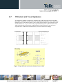
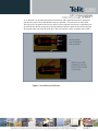
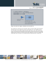
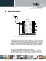
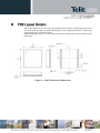
SPECIFICATIONS SUBJECT TO CHANGE WITHOUT NOTICE Notice While reasonable efforts have been made to assure the accuracy of this document, Telit assumes no liability resulting from any inaccuracies or omissions in this document, or from use of the information obtained herein. The information in this document has been carefully checked and is believed to be entirely reliable. However, no responsibility is assumed for inaccuracies or omissions. Telit reserves the right to make changes to any products described herein and reserves the right to revise this document and to make changes from time to time in content hereof with no obligation to notify any person of revisions or changes. Telit does not assume any liability arising out of the application or use of any product, software, or circuit described herein; neither does it convey license under its patent rights or the rights of others. It is possible that this publication may contain references to, or information about Telit products (machines and programs), programming, or services that are not announced in your country. Such references or information must not be construed to mean that Telit intends to announce such Telit products, programming, or services in your country. Copyrights This instruction manual and the Telit products described in this instruction manual may be, include or describe copyrighted Telit material, such as computer programs stored in semiconductor memories or other media. Laws in the Italy and other countries preserve for Telit and its licensors certain exclusive rights for copyrighted material, including the exclusive right to copy, reproduce in any form, distribute and make derivative works of the copyrighted material. Accordingly, any copyrighted material of Telit and its licensors contained herein or in the Telit products described in this instruction manual may not be copied, reproduced, distributed, merged or modified in any manner without the express written permission of Telit. Furthermore, the purchase of Telit products shall not be deemed to grant either directly or by implication, estoppel, or otherwise, any license under the copyrights, patents or patent applications of Telit, as arises by operation of law in the sale of a product. Computer Software Copyrights The Telit and 3rd Party supplied Software (SW) products described in this instruction manual may include copyrighted Telit and other 3rd Party supplied computer programs stored in semiconductor memories or other media. Laws in the Italy and other countries preserve for Telit and other 3rd Party supplied SW certain exclusive rights for copyrighted computer programs, including the exclusive right to copy or reproduce in any form the copyrighted computer program. Accordingly, any copyrighted Telit or other 3rd Party supplied SW computer programs contained in the Telit products described in this instruction manual may not be copied (reverse engineered) or reproduced in any manner without the express written permission of Telit or the 3rd Party SW supplier. Furthermore, the purchase of Telit products shall not be deemed to grant either directly or by implication, estoppel, or otherwise, any license under the copyrights, patents or patent applications of Telit or other 3rd Party supplied SW, except for the normal non-exclusive, royalty free license to use that arises by operation of law in the sale of a product. Usage and Disclosure Restrictions License Agreements The software described in this document is the property of Telit and its licensors. It is furnished by express license agreement only and may be used only in accordance with the terms of such an agreement. Copyrighted Materials Software and documentation are copyrighted materials. Making unauthorized copies is prohibited by law. No part of the software or documentation may be reproduced, transmitted, transcribed, stored in a retrieval system, or translated into any language or computer language, in any form or by any means, without prior written permission of Telit High Risk Materials Components, units, or third-party products used in the product described herein are NOT fault-tolerant and are NOT designed, manufactured, or intended for use as on-line control equipment in the following hazardous environments requiring fail-safe controls: the operation of Nuclear Facilities, Aircraft Navigation or Aircraft Communication Systems, Air Traffic Control, Life Support, or Weapons Systems (High Risk Activities"). Telit and its supplier(s) specifically disclaim any expressed or implied warranty of fitness for such High Risk Activities. Trademarks TELIT and the Stylized T Logo are registered in Trademark Office. All other product or service names are the property of their respective owners. Copyright © Telit Communications S.p.A. 2014. Contents The Telit SL871 is an OEM GNSS 9.7 x 10.1 x 2.5 mm receiver module based on the Mediatek MT3333 chip that supports All-in-One GNSS hybrid navigation. The Telit SL871 receiver provides extremely low power and very fast TTFF together with weak signal acquisition and tracking capability to meet even the most stringent performance expectations in hybrid navigation, using signals from both GPS + GLONASS+ Beidou GNSS systems. This document is intended for helping customer with new product design using the Telit SL871 GNSS module or for those customers wanting to adopt existing designs to industry standard existing modules. For general contact, technical support, to report documentation errors and to order manuals, contact Telit Technical Support Center (TTSC) at: [email protected] [email protected] [email protected] [email protected] Alternatively, use: http://www.telit.com/en/products/technical-support-center/contact.php For detailed information about where you can buy the Telit modules or for recommendations on accessories and components visit: http://www.telit.com To register for product news and announcements or for product questions contact Telit Technical Support Center (TTSC). Our aim is to make this guide as helpful as possible. Keep us informed of your comments and suggestions for improvements. Telit appreciates feedback from the users of our information. This document contains the following chapters (sample): “Chapter 1: “Introduction” provides a scope for this document, target audience, contact and support information, and text conventions. “Chapter 2: “Powering the SE868” gives an overview about power supply. “Chapter 3: “Updating Firmware” describes the SW updating procedure for Flash version. “Chapter 4: “Updating Patch code” describes how to apply patch code to ROM version. “Chapter 5: “Main serial interface” describes the serial interface. “Chapter 6: “MEMS sensor and EEPROM Interface” describes the DR I2C interface. “Chapter 7: “RF Front End Design” describes in details the characteristics of the Front end. “Chapter 8: “Reference Design” gives an overview about the reference design. “Chapter 9: “Firmware configuration” describes the configuration settings. “Chapter 10: “Handling and soldering” describes packaging and soldering of the module. “Chapter 11: “PCB layout details” describes the mechanical design of the module. “Chapter 12: “Document History” describes the history of the present product. Danger – This information MUST be followed or catastrophic equipment failure or bodily injury may occur. Caution or Warning – Alerts the user to important points about integrating the module, if these points are not followed, the module and end user equipment may fail or malfunction. Tip or Information – Provides advice and suggestions that may be useful when integrating the module. All dates are in ISO 8601 format, i.e. YYYY-MM-DD. SL871 Product Description, 80434ST10610A SL871 EVK User Guide, The SL871 has three power supply pins VCC, VBAT and VCC_RF The VCC pin provides the main supply voltage. When power is first applied the module will come up in a full power continuous operation mode. During operation, the current drawn by the module can vary by some orders of magnitude, especially if enabling low-power operation modes. Any supply must be able to handle the current fluctuation including any in rush surge current. GPS/GNSS positioning modules require a stable power supply. In selecting a strategy to achieve a clean and stable power supply, any resistance in the VCC supply line can negatively influence performance. Consider the following points: All supplies should be within the rated requirements. At the module input, use low ESR capacitors that can deliver the required current/charge for switching from backup mode to normal operation. At the module input, use low ESR capacitors that can deliver the required current/charge for switching from backup mode to normal operation. We recommend keeping the rail short and away from any noisy data lines or switching supplies, etc. Wide power lines and or even power planes are preferred. In case of a power failure on the module supply, VBAT supplies power to the real-time clock (RTC) and battery backed RAM (BBRAM). Use of valid time and the GNSS/GNSS orbit data at startup will improve the GPS/GNSS performance, i.e. enables hot and warm starts. If no backup battery is connected, the module performs a cold start at power up. If no battery backup is to be used connect this pin to the VCC supply. The VCC RF output voltage can provide voltage and current to an external active antenna or external LNA provided they are the same voltage level as VCC main supply. The VCC_RF can supply a maximum of 100mA and must be limited externally. The VCC_RF pin is connected internally to the VCC pin through a ferrite bead and bypass capacitor. This supply voltage is not switched. The Telit SL871 offers a power-optimized architecture with built-in autonomous power saving functions to minimize power consumption at any given time. The receiver operates in two modes: Continuous mode for best performance or Power Save mode for optimized power consumption. Power saving modes are listed below: Backup Mode Periodic mode Standby mode Always locate mode The SL871 powers up directly into full power continuous state. Continuous mode uses the acquisition engine at full performance resulting in the shortest possible TTFF and the highest sensitivity. It searches for all possible satellites until the almanac is completely downloaded. The receiver switches to the tracking engine to lower the power consumption when: • A valid GPS/GNSS position is obtained • The entire almanac has been downloaded • The ephemeris for each satellite in view is valid In the backup or hibernate state the receiver is in the lowest current consuming mode. The receiver operation is stopped; only the backup supply V_BAT is powered on while the main supply VCC can be switched off by the host. Waking up from Backup State to Full Power can be controlled by the host by switching on the VCC supply or After waking up, the receiver uses all available internal aiding, including GNSS time, Ephemeris, and Last Position, resulting in the fastest possible TTFF in either hot or warm start modes. During Backup State, the I/O block is powered off. The host should force its outputs to a low state or to a high-Z state during the Backup State to minimize small leakage currents (<10 μA typically) at Standby State In this mode, the receiver stops navigation, the internal processor enters standby state, and the current drain at main supply VCC is typically reduced to 0.4 mA. Enter standby mode by sending the NMEA command: $PMTK161,0*28. The host can wake up the module from Standby mode to Full Power mode by sending any byte via the host port. This mode allows autonomous power on/off with reduced fix rate to reduce average power consumption. The main power supply VCC is still active, but turning the supply on and off is controlled internally by NMEA commands. Enter periodic mode by sending the following NMEA command: $PMTK225,<Type>,<Run_time>,<Sleep_time>,<2nd_run_time>,<2nd_sleep_time>*<checksum> Where: • Type=1 for Periodic Backup mode • Run_time = Full Power period (ms) • Sleep_time = Standby/Backup period (ms) • 2nd_run_time = Full Power period (ms) for extended acquisition if GNSS acquisition fails during Run_time • 2nd_sleep_time = Standby/Backup period (ms) for extended sleep if GNSS acquisition fails during Run_time Example: $PMTK225,1,3000,12000,18000,72000*16 for periodic mode with 3 s navigation and 12 s sleep in backup state. The acknowledgement response for the command is $PMTK001,225,3*35. The module can exit Periodic mode by sending the command $PMTK225,0*2B just after the module wakes up from a previous sleep cycle. AlwaysLocate™ is an intelligent controller of the Periodic mode; the main power supply VCC is still active, but supply is controlled internally by PMTK commands. Depending on the environment and motion conditions, the module can autonomously and adaptively adjust the parameters of the Periodic mode, e.g. on/off ratio and fix rate to achieve a balance in positioning accuracy and power consumption. The average power drain can vary based on conditions; typical average power is 7 mW. Associated profiles are: High and Low Speed, Walking, Outdoor Static and Indoor. The module can control the embedded VCC power switch autonomously only after the SL871 is set to Periodic or to AlwaysLocate™ mode by a PMTK command. Enter AlwaysLocate™ mode by sending the following NMEA command: $PMTK225,<mode>*<checksum><CR><LF> Where mode=9 for AlwaysLocate™ in Backup mode. Example: $PMTK225,9*22. The acknowledgement response for the command is $PMTK001,225,3*35. The user can exit low power modes to Full Power by sending NMEA command $PMTK225,0*2B just after the module wakes up from its previous sleep cycle. The SL871 module includes a Universal Asynchronous Receiver Transmitter (UART) serial interface RxD/TxD that supports configurable baud rates. The signal output and input levels are 0 V to VCC. An interface based on RS232 standard levels (+/- 12 V) can be implemented using level shifters such as Maxim MAX3232. Hardware handshake signals and synchronous operation are not supported. Driving RESET_N low activates a hardware reset of the system. Use this pin only to reset the module. Do not use RESET_N to turn the module on and off, since the reset state increases power consumption. The TIMEPULSE (PPS) output signal provides a pulse-per-second output signal for timing purposes. The SL871 time pulse signal is one pulse per second. The PPS output is valid when navigation is valid and will also continue to ‘freewheel’ after a valid fix is lost by a certain navigation DR timeout of typically 10 seconds. Pulse length (high) is 100ms and UTC sync is at rising edge. The SL871 contains a pre-select SAW filter. This allows the SL871 to work well with a passive GNSS antenna. For improved performance or if the antenna cannot be located near the SL871, an active antenna (that is, an antenna with a low noise amplifier built in) can be used. The following items will be discussed in turn to assist in designing the “RF front end”. 1. RF signal requirements 2. GNSS antenna polarization 3. GNSS antenna gain 4. System noise floor 5. Active versus passive antenna 6. RF trace losses 7. Implications of the pre-select SAW filter 8. External LNA gain and Noise Figure 9. Powering the external LNA (active antenna) 10. RF interference 11. Shielding The SL871 can achieve Cold Start acquisition with a signal level of -148 dBm at its input. This means the SL871 can find the necessary satellites, download the necessary ephemeris data and compute the location within a 5 minute period. In the GNSS signal acquisition process, downloading and decoding the data is the most difficult task, which is why Cold Start acquisition requires a higher signal level than navigation or tracking signal levels. For the purposes of this discussion, autonomous operation is assumed, which makes the Cold Start acquisition level the important design constraint. If assistance data in the form of time or ephemeris aiding is available, then even lower signal levels can be used to compute a navigation solution. The GNSS signal is defined by IS-GNSS-200E. This document states that the signal level received by a linearly polarized antenna having 3 dBi gain will be a minimum of -130 dBm when the antenna is in the worst orientation and the satellite is 5 degrees or more above the horizon. In actual practice, the GNSS satellites are outputting slightly more power than specified by IS-GNSS-200E, and the signal level typically goes higher as the satellites have higher elevation angles. The SL871 will display a reported C/No of 40 dB-Hz for a signal level of -130 dBm at the RF input. Each GNSS satellite presents its own signal to the SL871, and best performance is obtained when the signal levels are between -130dbm and -125dBm. These received signal levels are determined by GNSS satellite transmit power GNSS satellite elevation and azimuth Free space path loss Extraneous path loss such as rain Partial or total path blockage such as foliage or building Multipath caused by signal reflection GNSS antenna Signal path after the GNSS antenna The first three items in the list above are specified in IS-GNSS-200E, readily available multiple sources online. IS-GNSS-200E specifies a signal level minimum of -130 dBm will be presented to the receiver when using a linearly polarized antenna with 3 dBi gain. The GNSS signal is relatively immune to rainfall attenuation and does not really need to be considered. However, the GNSS signal is heavily influence by attenuation due to foliage, such as tree canopies, etc. as well as outright blockage caused by building, terrain or other items in the line of sight to the specific GNSS satellite. This variable attenuation is highly dependent upon GNSS satellite location. If enough satellites are blocked, say at a lower elevation, or all in a general direction, the geometry of the remaining satellites will result is a lower accuracy of position. The SL871 reports this geometry in the form of PDOP, HDOP and VDOP. For example, in a vehicular application, the GNSS antenna may be placed embedded into the dashboard or rear package tray of an automobile. The metal roof of the vehicle will cause significant blockage, plus any thermal coating applied to the vehicle glass can attenuate the GNSS signal by as much as 15 dB. Again, both of these factors will affect the performance of the receiver. Multipath is a phenomena where the signal from a particular satellite is reflected and is received by the GNSS antenna in addition to or in place of the original line of sight signal. The multipath signal has a path length that is longer than the original line of sight path and can either attenuate the original signal, or if received in place of the original signal can add additional error in determining a solution, because the distance to the particular GNSS satellite is actually longer than expected. It is this phenomena that makes GNSS navigation in urban canyons (narrow roads surround by high rise buildings) so challenging. In general, the reflecting of the GNSS signal causes the polarization to reverse. The implications of this are covered in the next section. The GNSS signal as broadcast is a right hand circularly polarized signal. The best antenna to receive the GNSS signal is a right hand circularly (RHCP) polarized antenna. Remember that IS-GNSS-200E specifies the receive power level with a linearly polarized antenna. A linearly polarized antenna will have 3 dB loss as compared to an RHCP antenna assuming the same antenna gain (specified in dBi and dBic respectively). An RHCP antenna is better at rejecting multipath than a linearly polarized antenna. This is because the reflected signal changes polarization to LHCP, which would be rejected by the RHCP antenna by typically 20 dB or so. If the multipath signal is attenuating the line of sight signal, then the RHCP antenna would show a higher signal level than a linearly polarized antenna because the interfering signal is rejected. However, in the case where the multipath signal is replacing the line of sight signal, such as in an urban canyon environment, then the number of satellites in view could drop below that needed to determine a 3D solution. This is a case where a bad signal may be better than no signal. The system designer needs to make tradeoffs in their application to determine the better choice. Antenna gain is defined as the extra signal power from the antenna as compared to a theoretical isotropic antenna (equally sensitive in all directions). For example, a 25mm by 25m square patch antenna on a reference ground plane (usually 70mm by 70mm) will give an antenna gain at zenith of 5 dBic. A smaller 18mm by 18mm square patch on a reference ground plane (usually 50mm by 50mm) will give an antenna gain at zenith of 2 dBic. While an antenna vendor will specify a nominal antenna gain (usually at zenith, or directly overhead) they should supply antenna pattern curves specifying gain as a function of elevation, and gain at a fixed elevation as a function of azimuth. Pay careful attention to the requirement to meet these specifications, such as ground plane required and any external matching components. Failure to follow these requirements could result in very poor antenna performance. It is important to note that GNSS antenna gain is not the same thing as external LNA gain. Most antenna vendors will specify these numbers separately, but some combine them into a single number. It is important to know both numbers when designing and evaluating the front end of a GNSS receiver. For example, antenna X has an antenna gain of 5 dBic at azimuth and an LNA gain of 20 dB for a combined total of 25 dB. Antenna Y has an antenna gain of -5 dBiC at azimuth and an LNA gain of 30 dB for a combined total of 25 dB. However, in the system, antenna X will outperform antenna Y by about 10 dB (refer to Section 5.4 for more details on system noise floor). An antenna with higher gain will generally outperform an antenna with lower gain. Once the signals are above about -130 dBm for a particular satellite, no improvement in performance would be gained. However, for those satellites that are below about -125 dBm, a higher gain antenna would improve the gain and improve the performance of the GNSS receiver. In the case of really weak signals, a good antenna could mean the difference between being able to use a particular satellite signal or not. As mentioned earlier, the SL871 will display a reported C/No of 40 dB-Hz for an input signal level of -130 dBm. The C/No number means the carrier (or signal) is 40 dB greater than the noise floor measured in a one Hz bandwidth. This is a standard method of measuring GNSS receiver performance. The simplified formula is -174dbm + SNF – GNSS Signal level = C/No Thermal noise is -174 dBm/Hz at 290K. From this we can compute a system noise figure of 4 dB for the SL871. This noise figure consists of the loss of the pre-select SAW filter, the noise figure of the LNA as well as implementation losses within the digital signal processing unit. If a good quality external LNA is used with the SL871, then the noise figure of that LNA (typically better than 1dB) could reduce the overall system noise figure of the SL871 from 4 dB to around 2 dB. Some of the factors in the system noise figure are implementation losses due to quantization and other factors often referred to a digital noise or DSP noise and don’t scale with improved front end noise figure but are additive. The digital noise is typically around 1.0 -1.5dB. See Section 5.9 for more information about reducing system noise by adding an external LNA. If the GNSS antenna is placed near the SL871 and the RF trace losses are not excessive (nominally 1 dB), then a passive antenna can be used. This would normally be the lowest cost option and most of the time the simplest to use. However, if the antenna needs to be located away from the SL871 then an active antenna may be required to obtain the best system performance. The active antenna has its own built in low noise amplifier to overcome RF trace or cable losses after the active antenna. However, an active antenna has a low noise amplifier (LNA) with associated gain and noise figure. In addition, many active antennas have a pre-select filter, a post-select filter or both. RF Trace losses are difficult to estimate on a PCB without having the appropriate tables or RF simulation software to estimate what the losses would be. A good rule of thumb would be to keep the RF traces as short as possible, make sure they are 50 ohms impedance and don’t contain any sharp bends It’s important to maintain a 50ohm trace impedance on the RF path on the host board where the module is mounted to. Design software for calculating trace impedance can be found from multiple sources on the internet. Below is the Agilent design software AppCAD which can be downloaded for free. As you can see using a typical FR4 board stack up the calculated Trace width for this board is 900 microns or approximately 35mill. This may or may not be an acceptable trace width and board material may need to be adjusted accordingly. Figure 1 Typical Board stack and calculated trace width As is often the case board material may be dictated by other applications that are integrated onto the host board. The board thickness may be such that a very narrow trace may result. This may not be acceptable and can also lead to issues when the trace meets a component pad. In situation like this the ground layer directly under the RF trace path can be removed and the RF ground is then moved to the next layer. This can result in a more acceptable trace width. Figure 2 Avoid Narrow RF trace Figure 3 Wider Trace width achieved by moving ground plane The SL871 module contains a SAW filter used in a pre-select configuration with the built in LNA, meaning the RF input of the SL871 ties directly into the SAW filter. Any circuit connected to the input of the SL871 would see a complex impedance presented by the SAW filter, particularly out of band, rather than the relatively broad and flat return loss presented by the LNA. Filter devices pass the desired in band signal, resulting in low reflected energy (good return loss), and reject the out of band signal by reflecting it back to the input, resulting in high reflected energy (bad return loss). If an external amplifier is to be used with the SL871, the overall design should be checked for RF stability to prevent the external amplifier from oscillating. Amplifiers that are unconditionally stable at the output will be fine to use with the SL871. If an external filter is to be connected directly to the SL871, care needs to be used in making sure the external filter or the internal SAW filter performance is not compromised. These components are typically specified to operate into 50 ohms impedance, which is generally true in band, but would not be true out of band. If there is extra gain associated with the external filter, then a 6 dB Pi or T resistive attenuator is suggested to improve the impedance match between the two components. The SL871 can be used with an external LNA such as what might be found in an active antenna. Because of the internal LNA, the overall gain (including signal losses past the external LNA) should not exceed 14 dB. Levels higher than that can affect the jamming detection capability of the SL871. If a higher gain LNA is used, either a resistive Pi or T attenuator can be inserted after the LNA to bring the gain down to 14 dB. The external LNA should have a noise figure better than 1 dB. This will give an overall system noise figure of around 2 dB assuming the LNA gain is 14 dB, or if higher the low gain mode is selected within the SL871. The overall system noise figure can be calculated using the Friss formula for cascaded noise figure. The simplified formula is shown below. F is the total system noise, F1 is the noise figure of the external LNA, F2 is the noise figure of the internal LNA and G1 is the gain of the external LNA. In the GPS receiver the Digital noise is an additive number and cannot be reduced by reducing the System Nosie figure. Figure 4 Cascade Nosie Figure calculations with external LNA The external LNA, if having no pre-select filter, needs to be able to handle signals other than the GNSS signal. These signals are typically at much higher levels. The amplifier needs to stay in the linear region when presented with these other signals. Again, the system designer needs to determine all of the unintended signals and their possible levels that can be presented making sure the external LNA will not be driven into compression. If this were to happen, the GNSS signal itself would start to be attenuated and the GNSS performance would suffer. The external LNA needs a source of power. Many of the active antennas accept a 3 volt or 5 volt DC voltage that is impressed upon the RF signal line. This voltage is not supplied by the SL871, but can be easily supplied by the host design. Two approaches can be used. The first is to use an inductor to tie directly to the RF trace. This inductor should be at self-resonance at L1 (1.57542 GHz) and should have good Q for low loss. The higher the inductor Q, the lower the loss will be. The side of the inductor connecting to the antenna supply voltage should be bypassed to ground with a good quality RF capacitor, again operating at self-resonance at the L1 frequency. The second approach is to use a quarter wave stub in place of the inductor. The length of the stub is designed to be exactly a quarter wavelength, which has the effect of making an RF short at L1 at one end of the stub to appear as an RF open. The RF short is created by the good quality RF capacitor operating at self-resonance. The choice between the two would be determined by: RF path loss introduced by either the inductor or quarter wave stub. Cost of the inductor. Space availability for the quarter wave stub. Simulations done by Telit show the following: Murata LQG15HS27NJ02 Inductor 0.65 dB of additional signal loss Quarter wave stub on FR4 0.59 dB of additional signal loss Coilcraft B09TJLC Inductor (used in ref. design)0.37 dB of additional signal loss This additional loss occurs after the LNA so it is generally not significant unless the circuit is being designed to work with either an active or a passive antenna. RF Interference into the GNSS receiver tends to be the biggest problem when determining why the system performance is not meeting expectations. As mentioned earlier, the GNSS signals are at -130 dBm and lower. If signal higher than this are presented to the receiver it can be overwhelmed. The SL871 can reject up to 12 CW in-band jamming signals, but would still be affected by non-CW signals. The most common source of interference is digital noise. This is created by the fast rise and fall times and high clock speeds of modern digital circuitry. For example, a popular netbook computer uses an Atom processor clocked at 1.6 GHz. This is only 25 MHz away from the GNSS signal, and depending upon temperature of the SAW filter, can be within the passband of the GNSS receiver. Because of the nature of the address and data lines, this would be broadband digital noise at a relatively high level. Such devices are required to adhere to a regulatory standard for emissions such as FCC Part 15 Subpart J Class B or CISPR 22. However, these regulatory emission levels are far higher than the GNSS signal. Shielding the RF circuitry generally is ineffective because the interference is getting into the GNSS antenna itself, the most sensitive portion of the RF path. The antenna cannot be shielded because then it can’t receive the GNSS signals. There are two solutions, one is to move the antenna away from the source of interference or the second is to shield the digital interference to prevent it from getting to the antenna. The SL871 Reference Design is presented in the figure below. V_ANT C6 27pf SL871 Top View L1 35.5nH C5 100pf 10 GND 11 RFIN 12 GND 13 Reserved 14 VCC VRESET VCC Reserved 9 8 7 VCCBK 6 VCCRF Reserved 5 15 Reserved Timepulse 4 16 Reserved RxD 3 TX 17 Reserved TxD 2 RX 18 Reserved GND 1 Figure 4 – SL871 Reference Design – Active Antenna Along with power and ground, the minimum number of signals required to operate the SL871 properly are four digital signals and one RF signal. The RF input can be connected directly to a GNSS antenna. The reference design however shows a DC power feed for an active antenna. C5 is used to block the DC voltage from entering the SL871. The inductor L1 is chosen to be self-resonant at the GNSS frequency, approximately 1.57542 GHz, to minimize loading on the RF trace. Capacitor C6 is chosen to be self-resonant at the GNSS frequency such that is looks pretty close to an RF short at that frequency. V_ANT is the supply voltage for the external active antenna. Pin 7 can be connected to VCC for compatibly issues or left unconnected. TX is the normal digital output and as configured in the reference design, is a serial UART with a default bit rate of 9600 bps, 1 stop bit and 8 data bits. This is a 1.8 volt logic level signal. As is the case with all serial data, the idle state is logic one. RX is the normal digital input and as configured in the reference design, is a serial UART with a default bit rate of 4800 bps, 1 stop bit and 8 data bits. This is a 1.8 volt logic level signal, but is tolerant to 3.6 volts. As is the case with all serial data, the idle state is logic one. Be careful to tri-state this line if the SL871 is turned off to avoid back-driving the SL871.Firmware Configuration The SL871 can be configured by means of firmware in order to fit better into the overall system. This section describes certain aspects of the receiver that can be configured. The SL871 module can be operated in one of four power management modes; Full Power, Standby, Periodic, and Always Locate can be selected depending upon the requirements of the system design regarding frequency of position updates and availability of GNSS signals in the operational environment, The designer can choose a mode that provides the best trade-off of performance versus power consumption. Each of the power management modes can be commanded using the Serial commands which are available as part of the NEMA message set. More details regarding low power operation can be found in the Software Application Note. . The SL871 positioning module includes a Universal Asynchronous Receiver Transmitter (UART) serial interface RxD/TxD that supports configurable baud rates. For information about the supported baud rates, see the SL871 Software User Guide including Protocol Specification. The signal output and input levels are 0 V to VCC. An interface based on RS232 standard levels (+/- 12 V) can be implemented using level shifters such as Maxim MAX3232. Hardware handshake signals and synchronous operation are not supported. Static navigation, also called position pinning, is a mechanism that it is used by the receiver to freeze, or pin, the position when the velocity falls below a threshold indicating that the receiver is stationary. The heading is also frozen, and the velocity is reported as 0. The solution is then unpinned when the velocity increases above a threshold or when the computed position is a set distance from the pinned position, indicating that the receiver is in motion again. Note that these velocity and distance thresholds cannot be changed. By default static navigation is disabled. It can be enabled by sending a Static Navigation message command 1. This feature is useful for applications in which very low dynamics are not expected, the classic example being an automotive application. Velocity dead-reckoning refers to the use of the last known velocity to propagate the navigation solution when there are insufficient measurements to calculate an updated solution. It serves to mitigate the effects of blocked satellite signals by continuing to provide a position output. Note that the receiver outputs status information which indicates whether a solution is being maintained using dead-reckoning. By default the receiver operates in dead-reckoning mode for up to 10 seconds before invalidating the position. This timeout value is considered to be appropriate for most applications. It can be changed using the Mode Control message (Message ID 136). Valid timeout values are in a range from zero, which disables dead-reckoning, to two minutes. The SL871 module detects, tracks and removes narrow-band interfering signals (jammers) without the need for external components or tuning The Jamming Remover is an embedded interference suppression that tracks and removes up to 12 CW (Carrier Wave) type signals up to –80 dBm (total power signal levels). By default the interference suppression is disabled and usage requires a PMTK command to enable it. This is over and above the excellent SAW filter response that exists before the GPS LNA input. This feature is useful both in the design stage and during the production stage for uncovering issues related to unexpected jamming. The SL871 receiver is capable of using Satellite-Based Augmentation System (SBAS) satellites as a source of both differential corrections and satellite range measurements. These systems (WAAS, EGNOS, MSAS) use geostationary satellites to transmit regional differential corrections via a GNSS-compatible signal. The use of SBAS corrections can improve typical position accuracy to 3m or less in open-sky applications. Note that only an SBAS can be used as source of differential corrections. Other sources such as data from RTCM beacons are not supported. By default the SL871 does not attempt to acquire SBAS satellites. This can be changed by sending in a DGNSS Source and specifying the source of DGNSS corrections as SBAS. When the receiver acquires SBAS satellites, it will demodulate and use corrections data from the satellite signal. The receiver can be configured to compute SBAS satellite range measurements and use them in the navigation solution. This can be enabled software command. By default, the SL871 will compute a 2-D solution when possible when performing initial acquisition. In a 2-D solution, the receiver assumes a value for altitude and uses it to estimate the horizontal position. Under warm and hot start conditions, the receiver uses the last known value of altitude, which is a good assumption in most situations. However under cold start conditions, the last position is unknown, and the receiver assumes a value of 0. In situations where the true altitude is significantly higher than that, the horizontal position estimate will be noticeably impacted. To accommodate applications for which these situations are a concern, a version of SL871 firmware is offered that requires a calculated altitude, i.e. a 3-D navigational solution, in order for the receiver to first enter navigation. The SL871 module has a moisture sensitivity level rating of 3 as defined by IPC/JEDEC JSTD-020. This rating is assigned due to some of the components used within the SL871. The SL871 is supplied in trays or tape and reel and is hermetically sealed with desiccant and humidity indicator card. The SL871 parts must be placed and reflowed within 168 hours of first opening the hermetic seal provided the factory conditions are less than 30°C and less than 60% and the humidity indicator card indicates less than 10% relative humidity. If the package has been opened or the humidity indicator card indicates above 10%, then the parts will need to be baked prior to reflow. The parts may be baked at +125°C ± 5°C for 48 hours. However, the trays, nor the tape and reel can withstand that temperature. Lower temperature baking is feasible if the humidity level is low and time is available. Please see IPC/JEDEC J-STD-033 for additional information. Additional information can be found on the MSL tag affixed to the outside of the hermetical seal bag. NOTE: JEDEC standards are available for free from the JEDEC website http://www.jedec.org. Figure 5 Label for Moisture Sensitive Devices The SL871 is an electrostatic discharge sensitive device and should be handled in accordance with JESD625-A requirements for Handling Electrostatic Discharge Sensitive (ESDS) Devices. Although the SL871 is a module, the expecting handling of the SL871 during assembly and test is identical to that of a semiconductor device. Note: JEDEC standards are available for free from the JEDEC website http://www.jedec.org. The SL871 is compatible with lead free soldering processes as defined in IPC/JEDEC J-STD020. The reflow profile must not exceed the profile given in IPC/JEDEC J-STD-020 Table 52, “Classification Reflow Profiles”. Although IPC/JEDEC J-STD-020 allows for three reflows, the assembly process for the SL871 uses one of those profiles. Thus the SL871 is limited to two reflows. Note: JEDEC standards are available for free from the JEDEC website http://www.jedec.org. When reflowing a dual-sided SMT board, it is important to reflow the side containing the SL871 module last. This prevents heavier components within the SL871 becoming dislodged if the solder reaches liquidus temperature while the module is inverted. Due to the piezo-electric components within the SL871, the component should be placed close to the end of the assembly process to minimize shock to the module. During board singulation, pay careful attention to unwanted vibrations and resonances introduced into the board assembly by the board router. The PCB footprint on the receiving board should match the SL871 pad design shown below. The solder mask opening is generally determined by the component geometry of other parts on the board and can be followed here. Standard industry practice is to use a paste mask stencil opening the same dimensions as the pad design. Figure 6 – SL871 Mechanical Dimensions Revision 0 1 2 3 Date 2014-04-11 Changes First Preliminary issue