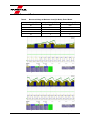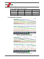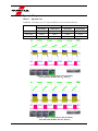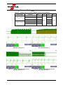
1
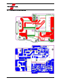
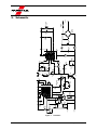
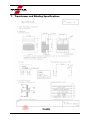
User Guide for FEBFAN6230AMPX_CH04U12A Evaluation Board Synchronous Rectification Controller 12.5 W (5 V / 2.5 A) Power Supply Using FAN6230A Featured Fairchild Products: FAN501 FAN6230A Direct questions or comments about this evaluation board to: “Worldwide Direct Support” Fairchild Semiconductor.com © 2014 Fairchild Semiconductor Corporation 1 FEBFAN6230AMPX_CH04U12A • Rev. 1.0 Table of Contents 1. Introduction ...................................................................................................................................... 3 1.1. General Description .................................................................................................................. 3 1.2. Features ..................................................................................................................................... 3 2. Evaluation Board Specifications ...................................................................................................... 4 3. Photographs ..................................................................................................................................... 5 4. Printed Circuit Board ....................................................................................................................... 6 5. Schematic ......................................................................................................................................... 7 6. Bill of Materials ............................................................................................................................... 8 7. Transformer and Winding Specifications ...................................................................................... 10 8. Test Conditions & Test Equipment................................................................................................ 13 9. Performance of Evaluation Board .................................................................................................. 14 9.1. Standby Power Consumption .................................................................................................. 14 9.2. Constant Voltage (CV) Regulation ......................................................................................... 15 9.3. Constant Current (CC) Regulation.......................................................................................... 16 9.4. Efficiency Test Result ............................................................................................................. 17 9.5. Output Ripple and Noise ......................................................................................................... 18 9.6. Normal Operation ................................................................................................................... 20 9.7. Turn-On Rising ....................................................................................................................... 21 9.8. Brownout Test......................................................................................................................... 22 9.9. VDD_1st&2st Voltage Level ......................................................................................................... 23 9.10. Maximum Power Level......................................................................................................... 24 9.11. Output Short Protection ........................................................................................................ 24 9.12. Dynamic Response................................................................................................................ 25 9.13. Voltage Stress on Drain_1st&2st ............................................................................................... 26 9.14. Conducted EMI Measurement .............................................................................................. 27 10. Revision History ............................................................................................................................ 28 © 2014 Fairchild Semiconductor Corporation 2 FEBFAN6230AMPX_CH04U12A • Rev. 1.0 This user guide supports the evaluation kit for the FAN6230A. It should be used in conjunction with the FAN6230A datasheet as well as Fairchild’s application notes and technical support team. Please visit Fairchild’s website at http://www.fairchildsemi.com. 1. Introduction This document is an engineering report describing measured performance of the FAN6230A evaluation board. 1.1. General Description The FAN6230A is a controller that improves efficiency in secondary-side Synchronous Rectifier (SR) MOSFETs. An internal shunt regulator with low bias current and an internal charge pump circuit reduce external part counts, total cost, and system power consumption. Adoption of the internal charge pump circuit allows the FAN6230A to work very well under low bias voltage conditions with good Constant Current (CC) regulation without a rectifier diode. FAN6230A also features adjustable cable compensation for precise constant voltage regulations at the cable end. Unlike the traditional method of measuring the SR MOSFET drain-to-source voltage to sense the current, which is sensitive to the noise introduced by poor PCB layout, the FAN6230A uses innovative Linear-Prediction Timing Control (LPC) to estimate the SR MOSFET turn-on time without additional current-sensing circuitry. In Green Mode, the FAN6230A shuts off the SR MOSFETs, which lowers bias current down to 500 µA, so the total power consumption of the system is further reduced. 1.2. Features Secondary-Side SR Controller for Flyback Converters Smooth Operation in DCM and CCM Integrated Shunt Regulator Integrated Charge Pump Circuit for CC Region Output Cable Compensation Circuit Green-Mode Improves Light-Load Efficiency and No-Load Power Consumption PWM Frequency Tracking Using Secondary-Side Winding Voltage Ultra Low VDD Operating Voltage for 5 V Output Applications Ultra-Low Green-Mode Operating Current (0.5 mA, Typical) 16-Pin MLP33 Package Advanced Protections - RES Dropping Protection (Disable Gate Drive) - Over-Temperature Protection (Auto-Restart) © 2014 Fairchild Semiconductor Corporation 3 FEBFAN6230AMPX_CH04U12A • Rev. 1.0 CN CP VCLAMP 5 VDD + VIN GATE 8 10 VCLAMP Internal Bias VLPC-EN Calculate VLPC-EN 15 RES tGREEN-ON / tGREEN-OFF Green Mode LPC 7 Charge Pump x2 9 VDD-ON/VDD-OFF 6 S + 2 16 VREF PWM Block 0.65V/1.25V Line Detection Function + - VCT Enable 1µA/V Period Detect RESET 1 CATHODE R Q + S - RESET iDISCHR iCHR Causal Function GATE Driver Q S Cable Comp. 0.445µA/V CT S S S 1.25V 14 13 11 4,12 COMRH COMRL PGND Figure 1. AGND Internal Block Diagram 2. Evaluation Board Specifications All data for this table was measured at an ambient temperature of 25°C Table 1. Evaluation Board Specifications Fairchild Devices FAN501 + FAN6230A Input Voltage Range 85 ~ 264 VAC Frequency 60 / 50 Hz Maximum Output Power 12.5 W Output Full-Load Condition 5 V / 2.5 A © 2014 Fairchild Semiconductor Corporation 4 FEBFAN6230AMPX_CH04U12A • Rev. 1.0 3. Photographs Figure 2. Figure 3. Figure 4. © 2014 Fairchild Semiconductor Corporation Top View (Dimension 45 x 32 [mm2]) Bottom View (Dimension 45 x 32 [mm2]) Flank View (Dimension 15 x 45 [mm2]) 5 FEBFAN6230AMPX_CH04U12A • Rev. 1.0 4. Printed Circuit Board Figure 5. Top Side Figure 6. © 2014 Fairchild Semiconductor Corporation Bottom Side 6 FEBFAN6230AMPX_CH04U12A • Rev. 1.0 5. Schematic AC IN F1 2A/250V U2 FOD817A D1~D4 FFM107 C6 470pF C1 12uF/400V R24 34kΩ L1 470uH C2 12uF/400V CL 0Ω SGND SD COMP FB U1 FAN501 6 4 7 5 8 HV R1 56kΩ GATE CS VS VDD 10 PGND R2 300K 9 1 2 3 R3 10Ω R6 0Ω C4 22uF C3 470pF/1kV NP TX1 RS 1.3Ω CY 100pF NA R19A 274kΩ Q1 FCU900N60Z D6 FFM107 R8 10Ω RS1 4.3Ω R23 17.4kΩ R9 56.2kΩ D5 1N4148 R5 100Ω R7 0Ω C7 27pF NS R19 221kΩ C5 1uF R12 10Ω C23 1nF 2 4 11 8 VIN 13 R33 3kΩ C11 390uF/6.3V R11 100kΩ C9 47nF 14 1 16 15 U2 FOD817A R32 910Ω C19 390uF/6.3V 3 LPC R31 0Ω 10 NC REF COMRH CATHODE RES 12 AGND AGND PGND COMRL VDD VCLAMP CN GATE Q2 FDMC86520L 5 6 7 9 C18 1uF CP R20 11kΩ U3 FAN6230_MLP C8 1uF R10 110kΩ R16 N.C R13 82kΩ R41 8.66kΩ R34 27.4kΩ R14 32.4kΩ C13 470pF CATHODE R30 24kΩ C14 100nF C12 47nF Vo (+) Vo (-) C15 6.8nF FEBFAN6230AMPX_CH04U12A • Rev. 1.0 7 © 2014 Fairchild Semiconductor Corporation Schematic Figure 7. 6. Bill of Materials Component Part No. Manufacturer Qty. Reference JUMPER WIRE 0.8 ψ (mm) 1 TH1 SMD Resistor 0603 0 Ω ±5% 2 R6, R7 SMD Resistor 0603 10 Ω ±5% 2 R8, R12 SMD Resistor 0603 100 Ω ±5% 1 R5 SMD Resistor 0603 100 kΩ ±5% 1 R11 SMD Resistor 0603 82 kΩ ±5% 1 R13 SMD Resistor 0603 11 kΩ ±1% 1 R20 SMD Resistor 0603 17 k 4 Ω ±1% 1 R23 SMD Resistor 0603 20 Ω ±5% 1 R31 SMD Resistor 0603 110 kΩ ±5% 1 R10 SMD Resistor 0603 221 kΩ ±1% 1 R19 SMD Resistor 0603 24 kΩ ±1% 1 R30 SMD Resistor 0603 27 k 4 Ω ±1% 1 R34 SMD Resistor 0603 274 kΩ ±1% 1 R19A SMD Resistor 0603 3 kΩ ±1% 1 R33 SMD Resistor 0603 32 k 4 Ω ±1% 1 R14 SMD Resistor 0603 34 kΩ ±1% 1 R24 SMD Resistor 0603 8 k 66 Ω ±1% 1 R41 SMD Resistor 0603 910 Ω ±5% 1 R32 SMD Resistor 0805 0 Ω ±5% 1 R22 SMD Resistor 0805 56 k 2 Ω ±1% 1 R9 SMD Resistor 1206 0 Ω ±5% 1 CL SMD Resistor 1206 10 Ω ±5% 1 R3 SMD Resistor 1206 1 Ω 3 ±5% 1 RS SMD Resistor 1206 300 kΩ ±5% 1 R2 SMD Resistor 1206 4 Ω 3 ±5% 1 RS1 SMD Resistor 1206 56 kΩ ±5% 1 R1 0603 X7R ±10% 0.1 µF 50 V 1 C14 0603 X7R ±10% 102 pF 50 V 1 C23 SMD 0603 105P 25 V +80/-20% 3 C5, C8, C18 0603 X7R ±10% 27 pF 50 V 1 C7 0603 X7R ±10% 471 pF 50 V 2 C6, C13 0603 X7R ±10% 473 pF 50 V 2 C9, C12 0603 X7R ±10% 682 pF 50 V 1 C15 1206 X5R ±10% 22 µF 10 V 1 C4 1206 X7R ±10% 471 pF 1 kV 1 C3 2 C1, C2 2 C11, C19 Electrolytic Capacitor 12 µF 400 V 105°C 8•16.5 mm, G-Luxon, GSM126M400T2H5G160 Capacitor 390 µF 6.3 V 105°C 5•9 mm, ULR Type, ULR397M0JD09RR © 2014 Fairchild Semiconductor Corporation 8 OS-CON FEBFAN6230AMPX_CH04U12A • Rev. 1.0 Bill of Materials (continued) Component Part No. Manufacturer Qty. Reference Y1 Capacitor 100P 250 V ±20% D7xF7xT9.5 mm 1 CY Fixed Inductor 470 μH ±10% EC0410-471K 1 L1 Transformer EEH1710 PN:14315-T001 SUMIDA 1 TX1 SMD Diode 1N4148WS 1 A / 100 V SOD-323 Fairchild 1 D5 SMD Diode FFM107-M 1 A / 1000 V SOD-123 5 D1, D2, D3, D4, D6 SMD MOS FDMC86520L 60 V 22 A Power33 Fairchild 1 Q2 MOS FCU900N60 Z 9 A / 600 V TO-251 Fairchild 1 Q1 FOD817AS SMD SMDIP-B 4 Pin Fairchild 1 U2 SMD IC FAN6230AMPX MLP Fairchild 1 U3 SMD IC FAN501MPX MLP Fairchild 1 U1 FUSE GLASS 250 V / 2 A Fast Blow 3.6•10 mm 36FG(L)R 1 F1 USB JC0010 4411-02004L Short Type 10•13 mm 1 J1 Teflon Tube 17 L x 305 m 3 TH1, C1, C2 MCH0223 Heat-Shrinkable Sleeve 6C15 1 H1 PCB PLM0286 REV0 For FAN501MPX 12.5 W 1 © 2014 Fairchild Semiconductor Corporation 9 FEBFAN6230AMPX_CH04U12A • Rev. 1.0 7. Transformer and Winding Specifications © 2014 Fairchild Semiconductor Corporation 10 FEBFAN6230AMPX_CH04U12A • Rev. 1.0 © 2014 Fairchild Semiconductor Corporation 11 FEBFAN6230AMPX_CH04U12A • Rev. 1.0 © 2014 Fairchild Semiconductor Corporation 12 FEBFAN6230AMPX_CH04U12A • Rev. 1.0 8. Test Conditions & Test Equipment Evaluation Board FEBFAN6230AMPX_CH04U12A Test Date December 16, 2014 Test Equipment AC Source: 6800 Series Electronic Load: Chroma 63030 Oscilloscope: LeCroy 24Xs-A Power Meter: Yokogawa WT210 Test Items 1. Standby Power Consumption 2. CV (Constant Voltage) Regulation 3. CC (Constant Current) Regulation 4. Efficiency Test Result 5. Output Ripple and Noise 6. Normal Operation 7. Turn-On Rising 8. Brownout Test 9. VDD_1st&2st Voltage Level 10. Maximum Power Level 11. Output Short Protection 12. Dynamic Response 13. Voltage Stress of Drain_1st&2st 14. Conducted EMI Measurement © 2014 Fairchild Semiconductor Corporation 13 FEBFAN6230AMPX_CH04U12A • Rev. 1.0 9. Performance of Evaluation Board 9.1. Standby Power Consumption Table 2. Standby Power Consumption at No-Load Condition VIN 85 V 115 V 230 V 264 V No Load 15.7 mW 14.9 mW 18.7 mW 19.3 mW Figure 8. Entry Green Mode, No SR Gate Enable, No Load, 85 VAC, Full-Load (CH1: DET, CH2: SR VDD, CH3: SR Gate, CH4: VOUT) Figure 9. Entry Green Mode, No SR Gate Enable, No Load, 264 VAC, Full-Load (CH1: DET, CH2: SR VDD, CH3: SR Gate, CH4: VOUT) © 2014 Fairchild Semiconductor Corporation 14 FEBFAN6230AMPX_CH04U12A • Rev. 1.0 9.2. Constant Voltage (CV) Regulation Table 3. CV Regulation Enable COMR Max. Min. Reg. With USB Cable 5.285 V 5.116 V 1.68% Without USB Cable 5.806 V 5.191 V 6.15% © 2014 Fairchild Semiconductor Corporation Figure 10. Enable COMR, CV Curve Measure, End of Board Figure 11. Enable COMR, CV Curve Measure, End of Cable 15 FEBFAN6230AMPX_CH04U12A • Rev. 1.0 9.3. Constant Current (CC) Regulation Table 4. CC Regulation Enable COMR With USB Cable Figure 12. © 2014 Fairchild Semiconductor Corporation Max. Min. Reg. 2.75 A 2.48 A 5.41% Enable COMR, CC Curve Measure in End of Cable 16 FEBFAN6230AMPX_CH04U12A • Rev. 1.0 9.4. Efficiency Test Result Table 5. Efficiency Test Results, Including 10% of Efficiency VIN 10% 25% 50% 75% 100% Avg. 85 VIN / 60 Hz 77.63% 84.73% 87.27% 87.82% 87.10% 86.73% 115 VIN / 60 Hz 77.44% 85.58% 86.95% 88.10% 88.73% 87.34% 230 VIN / 50 Hz 72.26% 80.25% 86.55% 88.04% 88.64% 85.87% 264 VIN / 50 Hz 71.02% 80.11% 85.46% 87.25% 88.22% 85.26% Test Method: Test after 15 minutes aging - Test from heavy load to light load Figure 13. © 2014 Fairchild Semiconductor Corporation Efficiency vs. Output Load and Input Voltage 17 FEBFAN6230AMPX_CH04U12A • Rev. 1.0 9.5. Output Ripple and Noise Figure 14. Table 6. Recommended Test Setup Maximum Output Ripple, End of Board VIN 85 V 115 V 230 V 264 V Vpp(Max.) 125 mV 105 mV 117 mV 115 mV Figure 15. © 2014 Fairchild Semiconductor Corporation Ripple vs. Output Current and Input Voltage 18 FEBFAN6230AMPX_CH04U12A • Rev. 1.0 © 2014 Fairchild Semiconductor Corporation Figure 16. 85 VAC, Full-Load (CH4: VOUT) Figure 17. 264 VAC, Full-Load (CH4: VOUT) 19 FEBFAN6230AMPX_CH04U12A • Rev. 1.0 9.6. Normal Operation Figure 18. tdeadtime=878 ns, 85 VAC, Full-Load (CH1: DET, CH3: SR Gate) Figure 19. Figure 20. tdeadtime=887 ns, 230 VAC, Full-Load (CH1: DET, CH3: SR Gate) © 2014 Fairchild Semiconductor Corporation tdeadtime=943 ns, 115 VAC, Full-Load (CH1: DET, CH3: SR Gate) Figure 21. tdeadtime=887 ns, 264 VAC, Full-Load (CH1: DET, CH3: SR Gate) 20 FEBFAN6230AMPX_CH04U12A • Rev. 1.0 9.7. Turn-On Rising Table 7. Measurement Output Voltage of 10% to 90%, End of Cable trising Loading 85 VIN 115 VIN 230 VIN 264 VIN No Load 10 ms 13 ms 12.9 ms 12 ms Full Load 10 ms 11.1 ms 10 ms 12 ms Figure 22. 85 VAC, Full-Load (CH1: DET, CH2: SR VDD, CH3: SR VDD, CH4: VOUT) Figure 23. 264 VAC, Full-Load (CH1: DET, CH2: SR VDD, CH3: SR VDD, CH4: VOUT) © 2014 Fairchild Semiconductor Corporation 21 FEBFAN6230AMPX_CH04U12A • Rev. 1.0 9.8. Brownout Test Table 8. Brownout Voltage at Maximum Load (CC Mode), End of Board Input Voltage (V) Input Wattage (W) Output Voltage (V) 90 16.11 5.59 80 16.08 5.51 70 16.18 5.51~5.06 60 14.70 5.51~3.11 53 0 0 Figure 24. 54 VAC, Full-Load (CH1: DET, CH2: SR VDD, CH4: VOUT) Figure 25. 54 VAC, Full-Load (CH1: DET, CH2: SR VDD, CH4: VOUT) © 2014 Fairchild Semiconductor Corporation 22 FEBFAN6230AMPX_CH04U12A • Rev. 1.0 9.9. VDD_1st&2st Voltage Level Table 9. VDD with Control IC of Primary and Secondary Sides VIN No Load Max. Load Near OPP (V) VDD_1st VDD_2st VDD_1st VDD_2st VDD_1st VDD_2st 85 V / 60 Hz 10.36 V 4.49 V 17.34 V 5.04 V 17.71 V 5.04 V 264 V / 50 Hz 10.15 V 4.50 V 18.33 V 5.09 V 18.8 V 5.09 V Figure 26. 85 VAC, Near OPP (CH1: DET, CH2: SR VDD, CH3: SR Gate, CH4: VDD_1st) Figure 27. 264 VAC, Near Over-Power Protection (CH1: DET, CH2: SR VDD, CH3: SR Gate, CH4: VDD_1st) © 2014 Fairchild Semiconductor Corporation 23 FEBFAN6230AMPX_CH04U12A • Rev. 1.0 9.10. Maximum Power Level Table 10. Maximum Power Level, End of Board Input Voltage Output Current (A) Output Voltage (V) Output Wattage (W) 85 V / 60 Hz 2.74 5.546 15.18 115 V / 60 Hz 2.71 5.722 15.53 230 V / 60 Hz 2.68 5.802 15.56 264 V / 60 Hz 2.69 5.836 15.73 9.11. Output Short Protection Figure 28. 85 VAC, Short at Full Load (CC Mode) (CH1: DET, CH2: SR Gate, CH3: SR VDD, CH4: VO) Figure 29. 264 VAC, Short at Full Load (CC Mode) (CH1: DET, CH2: SR Gate, CH3: SR VDD, CH4: VO) © 2014 Fairchild Semiconductor Corporation 24 FEBFAN6230AMPX_CH04U12A • Rev. 1.0 9.12. Dynamic Response Table 11. Dynamic Test Conditions: 5 ms duty cycle, 2.5 A/µs rise/fall time, level in end of cable line 85 VIN 264 VIN Overshoot Undershoot Overshoot Undershoot 0%~50% 5.315 V 4.670 V 5.360 V 4.665 V 50%~100% 5.380 V 4.935 V 5.535 V 5.010 V 0%~100% 5.375 V 4.335 V 5.500 V 4.315 V Figure 30. 85 VAC, Loading of 0%~100% (CC Mode) (CH1: DET, CH2: SR Gate, CH3: VFB, CH4: VO) Figure 31. 264 VAC, Loading of 0%~100% (CC Mode) (CH1: DET, CH2: SR Gate, CH3: VFB, CH4: VO) © 2014 Fairchild Semiconductor Corporation 25 FEBFAN6230AMPX_CH04U12A • Rev. 1.0 9.13. Voltage Stress on Drain_1st&2st Table 12. Voltage Stress on Primary MOSFET and Secondary MOSFET Input Voltage Condition Drain_1st Full Load 277 V 22.2 V 85 VIN / 60 Hz Startup at Full Load 279 V 22.2 V Short at Full Load 266 V Full Load 560 V Startup at Full Load 557 V 43.9 V Short at Full Load 544 V 42.3 V 264 VIN / 50 Hz Figure 32. 85 VAC, AC Start at Full-Load (CH1: DET, CH3: Drain-1st) Figure 34. 600 V Drain_2st 20.25 V 44.2 V Rating 60 V Figure 33. 264 VAC, AC Start at Full-Load (CH1: DET, CH3: Drain-1st) 85 VAC, Output Short at Full-Load (CH1: DET, CH3: Drain-1st) © 2014 Fairchild Semiconductor Corporation Rating Figure 35. 26 264 VAC, Output Short at Full-Load (CH1: DET, CH3: Drain-1st) FEBFAN6230AMPX_CH04U12A • Rev. 1.0 9.14. Conducted EMI Measurement Att dBµV 1 100 10 dB RBW 9 MT 10 PREAMP OFF kHz ms MHz Att 10 MHz dBµV 90 1 RBW 9 MT 10 PREAMP OFF kHz ms MHz 10 MHz PK MAXH 80 2 AV MAXH dB 90 1 PK MAXH 1 100 10 2 TDF 70 80 AV MAXH EN55022Q TDF 70 EN55022Q 60 60 PRN EN55022A PRN EN55022A 50 50 6DB 6DB 40 40 30 30 20 20 10 10 0 0 150 Comment: kHz 30 Comment: 2-230N Date: 10.SEP.2013 Date: 18:22:16 Figure 36. Att dBµV 150 MHz 1 100 10 dB RBW 9 MT 10 PREAMP OFF MHz 10.SEP.2013 Nature at 115 VAC kHz ms Att 10 MHz dBµV MHz 18:18:21 Figure 37. 1 100 10 dB MHz RBW 9 MT 10 PREAMP OFF kHz ms 10 MHz 90 1 PK 1 PK MAXH 80 2 AV MAXH 30 2-230N Line at 115 VAC 90 MAXH kHz 2 TDF 70 80 AV MAXH EN55022Q TDF 70 EN55022Q 60 60 PRN EN55022A PRN EN55022A 50 50 6DB 6DB 40 40 30 30 20 20 10 10 0 0 150 Comment: Date: kHz 30 150 MHz Comment: 2-230N 10.SEP.2013 Date: 18:28:09 Figure 38. Line at 115 VAC © 2014 Fairchild Semiconductor Corporation kHz 30 2-230N 10.SEP.2013 18:32:36 Figure 39. 27 MHz Nature at 115 VAC FEBFAN6230AMPX_CH04U12A • Rev. 1.0 10. Revision History Rev. Date Description 1.0 12/2014 Initial release WARNING AND DISCLAIMER Replace components on the Evaluation Board only with those parts shown on the parts list (or Bill of Materials) in the Users’ Guide. Contact an authorized Fairchild representative with any questions. This board is intended to be used by certified professionals, in a lab environment, following proper safety procedures. Use at your own risk. The Evaluation board (or kit) is for demonstration purposes only and neither the Board nor this User’s Guide constitute a sales contract or create any kind of warranty, whether express or implied, as to the applications or products involved. Fairchild warrantees that its products meet Fairchild’s published specifications, but does not guarantee that its products work in any specific application. Fairchild reserves the right to make changes without notice to any products described herein to improve reliability, function, or design. Either the applicable sales contract signed by Fairchild and Buyer or, if no contract exists, Fairchild’s standard Terms and Conditions on the back of Fairchild invoices, govern the terms of sale of the products described herein. DISCLAIMER FAIRCHILD SEMICONDUCTOR RESERVES THE RIGHT TO MAKE CHANGES WITHOUT FURTHER NOTICE TO ANY PRODUCTS HEREIN TO IMPROVE RELIABILITY, FUNCTION, OR DESIGN. FAIRCHILD DOES NOT ASSUME ANY LIABILITY ARISING OUT OF THE APPLICATION OR USE OF ANY PRODUCT OR CIRCUIT DESCRIBED HEREIN; NEITHER DOES IT CONVEY ANY LICENSE UNDER ITS PATENT RIGHTS, NOR THE RIGHTS OF OTHERS. LIFE SUPPORT POLICY FAIRCHILD’S PRODUCTS ARE NOT AUTHORIZED FOR USE AS CRITICAL COMPONENTS IN LIFE SUPPORT DEVICES OR SYSTEMS WITHOUT THE EXPRESS WRITTEN APPROVAL OF THE PRESIDENT OF FAIRCHILD SEMICONDUCTOR CORPORATION. As used herein:. 1. Life support devices or systems are devices or systems which, (a) are intended for surgical implant into the body, or (b) support or sustain life, or (c) whose failure to perform when properly used in accordance with instructions for use provided in the labeling, can be reasonably expected to result in significant injury to the user. 2. A critical component is any component of a life support device or system whose failure to perform can be reasonably expected to cause the failure of the life support device or system, or to affect its safety or effectiveness. ANTI-COUNTERFEITING POLICY Fairchild Semiconductor Corporation's Anti-Counterfeiting Policy. Fairchild's Anti-Counterfeiting Policy is also stated on our external website, www.fairchildsemi.com, under Sales Support. Counterfeiting of semiconductor parts is a growing problem in the industry. All manufacturers of semiconductor products are experiencing counterfeiting of their parts. Customers who inadvertently purchase counterfeit parts experience many problems such as loss of brand reputation, substandard performance, failed applications, and increased cost of production and manufacturing delays. Fairchild is taking strong measures to protect ourselves and our customers from the proliferation of counterfeit parts. Fairchild strongly encourages customers to purchase Fairchild parts either directly from Fairchild or from Authorized Fairchild Distributors who are listed by country on our web page cited above. Products customers buy either from Fairchild directly or from Authorized Fairchild Distributors are genuine parts, have full traceability, meet Fairchild's quality standards for handling and storage and provide access to Fairchild's full range of up-to-date technical and product information. Fairchild and our Authorized Distributors will stand behind all warranties and will appropriately address any warranty issues that may arise. Fairchild will not provide any warranty coverage or other assistance for parts bought from Unauthorized Sources. Fairchild is committed to combat this global problem and encourage our customers to do their part in stopping this practice by buying direct or from authorized distributors. EXPORT COMPLIANCE STATEMENT These commodities, technology, or software were exported from the United States in accordance with the Export Administration Regulations for the ultimate destination listed on the commercial invoice. Diversion contrary to U.S. law is prohibited. U.S. origin products and products made with U.S. origin technology are subject to U.S Re-export laws. In the event of re-export, the user will be responsible to ensure the appropriate U.S. export regulations are followed. © 2014 Fairchild Semiconductor Corporation 28 FEBFAN6230AMPX_CH04U12A • Rev. 1.0