1
Serial Digital Interface (SDI) MegaCore Function User
Guide
Serial Digital Interface (SDI) MegaCore Function
User Guide
101 Innovation Drive
San Jose, CA 95134
www.altera.com
UG-SDI1005-16.0
Document last updated for Altera Complete Design Suite version:
Document publication date:
12.1
February 2013
Feedback Subscribe
© 2013 Altera Corporation. All rights reserved. ALTERA, ARRIA, CYCLONE, HARDCOPY, MAX, MEGACORE, NIOS, QUARTUS and STRATIX words and logos
are trademarks of Altera Corporation and registered in the U.S. Patent and Trademark Office and in other countries. All other words and logos identified as
trademarks or service marks are the property of their respective holders as described at www.altera.com/common/legal.html. Altera warrants performance of its
semiconductor products to current specifications in accordance with Altera's standard warranty, but reserves the right to make changes to any products and
services at any time without notice. Altera assumes no responsibility or liability arising out of the application or use of any information, product, or service
described herein except as expressly agreed to in writing by Altera. Altera customers are advised to obtain the latest version of device specifications before relying
on any published information and before placing orders for products or services.
February 2013
Altera Corporation
ISO
9001:2008
Registered
Serial Digital Interface (SDI) MegaCore Function
User Guide
Contents
Chapter 1. About This MegaCore Function
Features . . . . . . . . . . . . . . . . . . . . . . . . . . . . . . . . . . . . . . . . . . . . . . . . . . . . . . . . . . . . . . . . . . . . . . . . . . . . . . . . 1–1
Release Information . . . . . . . . . . . . . . . . . . . . . . . . . . . . . . . . . . . . . . . . . . . . . . . . . . . . . . . . . . . . . . . . . . . . . 1–2
Device Family Support . . . . . . . . . . . . . . . . . . . . . . . . . . . . . . . . . . . . . . . . . . . . . . . . . . . . . . . . . . . . . . . . . . . 1–2
General Description . . . . . . . . . . . . . . . . . . . . . . . . . . . . . . . . . . . . . . . . . . . . . . . . . . . . . . . . . . . . . . . . . . . . . 1–3
OpenCore Plus Evaluation . . . . . . . . . . . . . . . . . . . . . . . . . . . . . . . . . . . . . . . . . . . . . . . . . . . . . . . . . . . . . 1–5
Resource Utilization . . . . . . . . . . . . . . . . . . . . . . . . . . . . . . . . . . . . . . . . . . . . . . . . . . . . . . . . . . . . . . . . . . . . . 1–6
Chapter 2. Getting Started
Design Flow . . . . . . . . . . . . . . . . . . . . . . . . . . . . . . . . . . . . . . . . . . . . . . . . . . . . . . . . . . . . . . . . . . . . . . . . . . . . 2–1
SDI Walkthrough . . . . . . . . . . . . . . . . . . . . . . . . . . . . . . . . . . . . . . . . . . . . . . . . . . . . . . . . . . . . . . . . . . . . . . . . 2–3
Creating a New Quartus II Project . . . . . . . . . . . . . . . . . . . . . . . . . . . . . . . . . . . . . . . . . . . . . . . . . . . . . . . 2–3
Launching MegaWizard Plug-In Manager . . . . . . . . . . . . . . . . . . . . . . . . . . . . . . . . . . . . . . . . . . . . . . . . 2–4
Parameterizing . . . . . . . . . . . . . . . . . . . . . . . . . . . . . . . . . . . . . . . . . . . . . . . . . . . . . . . . . . . . . . . . . . . . . . . 2–5
Setting Up Simulation . . . . . . . . . . . . . . . . . . . . . . . . . . . . . . . . . . . . . . . . . . . . . . . . . . . . . . . . . . . . . . . . . 2–6
Generating Files . . . . . . . . . . . . . . . . . . . . . . . . . . . . . . . . . . . . . . . . . . . . . . . . . . . . . . . . . . . . . . . . . . . . . . 2–6
Simulating the Design . . . . . . . . . . . . . . . . . . . . . . . . . . . . . . . . . . . . . . . . . . . . . . . . . . . . . . . . . . . . . . . . . . . . 2–8
Testbench . . . . . . . . . . . . . . . . . . . . . . . . . . . . . . . . . . . . . . . . . . . . . . . . . . . . . . . . . . . . . . . . . . . . . . . . . . . . 2–8
Simulate with IP Functional Simulation Models . . . . . . . . . . . . . . . . . . . . . . . . . . . . . . . . . . . . . . . . . . . 2–9
Simulating with the ModelSim Simulator . . . . . . . . . . . . . . . . . . . . . . . . . . . . . . . . . . . . . . . . . . . . . . . . 2–9
Simulating in Third-Party Simulation Tools Using NativeLink . . . . . . . . . . . . . . . . . . . . . . . . . . . . . 2–10
Specifying Constraints . . . . . . . . . . . . . . . . . . . . . . . . . . . . . . . . . . . . . . . . . . . . . . . . . . . . . . . . . . . . . . . . . . 2–11
Single Channel . . . . . . . . . . . . . . . . . . . . . . . . . . . . . . . . . . . . . . . . . . . . . . . . . . . . . . . . . . . . . . . . . . . . . . 2–11
Multiple Channels . . . . . . . . . . . . . . . . . . . . . . . . . . . . . . . . . . . . . . . . . . . . . . . . . . . . . . . . . . . . . . . . . . . 2–12
Compiling the Design . . . . . . . . . . . . . . . . . . . . . . . . . . . . . . . . . . . . . . . . . . . . . . . . . . . . . . . . . . . . . . . . . . . 2–14
Programming a Device . . . . . . . . . . . . . . . . . . . . . . . . . . . . . . . . . . . . . . . . . . . . . . . . . . . . . . . . . . . . . . . . . . 2–14
Setting Up Licensing . . . . . . . . . . . . . . . . . . . . . . . . . . . . . . . . . . . . . . . . . . . . . . . . . . . . . . . . . . . . . . . . . . . . 2–15
Chapter 3. Functional Description
Block Description . . . . . . . . . . . . . . . . . . . . . . . . . . . . . . . . . . . . . . . . . . . . . . . . . . . . . . . . . . . . . . . . . . . . . . . 3–2
Transmitter . . . . . . . . . . . . . . . . . . . . . . . . . . . . . . . . . . . . . . . . . . . . . . . . . . . . . . . . . . . . . . . . . . . . . . . . . . 3–2
HD-SDI LN Insertion . . . . . . . . . . . . . . . . . . . . . . . . . . . . . . . . . . . . . . . . . . . . . . . . . . . . . . . . . . . . . . . 3–4
HD-SDI CRC Generation and Insertion . . . . . . . . . . . . . . . . . . . . . . . . . . . . . . . . . . . . . . . . . . . . . . . . 3–4
Scrambling and NRZI Coding . . . . . . . . . . . . . . . . . . . . . . . . . . . . . . . . . . . . . . . . . . . . . . . . . . . . . . . . 3–5
Transceiver Clock . . . . . . . . . . . . . . . . . . . . . . . . . . . . . . . . . . . . . . . . . . . . . . . . . . . . . . . . . . . . . . . . . . 3–5
Receiver . . . . . . . . . . . . . . . . . . . . . . . . . . . . . . . . . . . . . . . . . . . . . . . . . . . . . . . . . . . . . . . . . . . . . . . . . . . . . 3–6
NRZI Decoding and Descrambling . . . . . . . . . . . . . . . . . . . . . . . . . . . . . . . . . . . . . . . . . . . . . . . . . . . . 3–8
Word Alignment . . . . . . . . . . . . . . . . . . . . . . . . . . . . . . . . . . . . . . . . . . . . . . . . . . . . . . . . . . . . . . . . . . . 3–8
Video Timing Flags Extraction . . . . . . . . . . . . . . . . . . . . . . . . . . . . . . . . . . . . . . . . . . . . . . . . . . . . . . . 3–9
RP168 Switching Compliance . . . . . . . . . . . . . . . . . . . . . . . . . . . . . . . . . . . . . . . . . . . . . . . . . . . . . . . . 3–9
HD-SDI LN Extraction . . . . . . . . . . . . . . . . . . . . . . . . . . . . . . . . . . . . . . . . . . . . . . . . . . . . . . . . . . . . . 3–10
HD-SDI CRC Checking . . . . . . . . . . . . . . . . . . . . . . . . . . . . . . . . . . . . . . . . . . . . . . . . . . . . . . . . . . . . . 3–10
Accessing Transceiver . . . . . . . . . . . . . . . . . . . . . . . . . . . . . . . . . . . . . . . . . . . . . . . . . . . . . . . . . . . . . . 3–10
Transceiver Clock . . . . . . . . . . . . . . . . . . . . . . . . . . . . . . . . . . . . . . . . . . . . . . . . . . . . . . . . . . . . . . . . . 3–12
Transceiver—Soft-Logic Implementation . . . . . . . . . . . . . . . . . . . . . . . . . . . . . . . . . . . . . . . . . . . . . . . . 3–12
Transmitter . . . . . . . . . . . . . . . . . . . . . . . . . . . . . . . . . . . . . . . . . . . . . . . . . . . . . . . . . . . . . . . . . . . . . . . 3–12
Transmitter Clocks . . . . . . . . . . . . . . . . . . . . . . . . . . . . . . . . . . . . . . . . . . . . . . . . . . . . . . . . . . . . . . . . . 3–12
Receiver . . . . . . . . . . . . . . . . . . . . . . . . . . . . . . . . . . . . . . . . . . . . . . . . . . . . . . . . . . . . . . . . . . . . . . . . . . 3–13
February 2013
Altera Corporation
Serial Digital Interface (SDI) MegaCore Function
User Guide
iv
Contents
Receiver Clocks . . . . . . . . . . . . . . . . . . . . . . . . . . . . . . . . . . . . . . . . . . . . . . . . . . . . . . . . . . . . . . . . . . . 3–13
Transceiver—Stratix GX Devices . . . . . . . . . . . . . . . . . . . . . . . . . . . . . . . . . . . . . . . . . . . . . . . . . . . . . . . 3–13
Transmitter Clocks . . . . . . . . . . . . . . . . . . . . . . . . . . . . . . . . . . . . . . . . . . . . . . . . . . . . . . . . . . . . . . . . . 3–13
Receiver Clocks . . . . . . . . . . . . . . . . . . . . . . . . . . . . . . . . . . . . . . . . . . . . . . . . . . . . . . . . . . . . . . . . . . . 3–15
Transmitter Transceiver Interface . . . . . . . . . . . . . . . . . . . . . . . . . . . . . . . . . . . . . . . . . . . . . . . . . . . . 3–16
Receiver Transceiver Interface . . . . . . . . . . . . . . . . . . . . . . . . . . . . . . . . . . . . . . . . . . . . . . . . . . . . . . . 3–17
Transceiver—Arria GX, Arria II GX, Arria V, Cyclone IV GX, Cyclone V, Stratix II GX, Stratix IV GX,
and Stratix V Devices . . . . . . . . . . . . . . . . . . . . . . . . . . . . . . . . . . . . . . . . . . . . . . . . . . . . . . . . . . . . . . . . . 3–18
Transmitter Clocks . . . . . . . . . . . . . . . . . . . . . . . . . . . . . . . . . . . . . . . . . . . . . . . . . . . . . . . . . . . . . . . . . 3–19
Receiver Clocks . . . . . . . . . . . . . . . . . . . . . . . . . . . . . . . . . . . . . . . . . . . . . . . . . . . . . . . . . . . . . . . . . . . 3–22
Transmitter Transceiver Interface . . . . . . . . . . . . . . . . . . . . . . . . . . . . . . . . . . . . . . . . . . . . . . . . . . . . 3–23
Receiver Transceiver Interface . . . . . . . . . . . . . . . . . . . . . . . . . . . . . . . . . . . . . . . . . . . . . . . . . . . . . . . 3–24
Locking to the Incoming SDI Stream . . . . . . . . . . . . . . . . . . . . . . . . . . . . . . . . . . . . . . . . . . . . . . . . . . . . 3–25
Transceiver Dynamic Reconfiguration for Dual Standard and Triple Standard Receivers . . . . . . 3–27
Transceiver Dynamic Reconfiguration with Channel Reconfiguration Mode—Arria II GX,
HardCopy IV GX, Stratix GX, Stratix II GX, and
Stratix IV GX . . . . . . . . . . . . . . . . . . . . . . . . . . . . . . . . . . . . . . . . . . . . . . . . . . . . . . . . . . . . . . . . . . . . . . 3–27
Transceiver Dynamic Reconfiguration with PLL Reconfiguration Mode—Cyclone IV GX . . . 3–33
Reset Requirement During Reconfiguration . . . . . . . . . . . . . . . . . . . . . . . . . . . . . . . . . . . . . . . . . . . 3–36
OpenCore Plus Time-Out Behavior . . . . . . . . . . . . . . . . . . . . . . . . . . . . . . . . . . . . . . . . . . . . . . . . . . . . . 3–39
Signals . . . . . . . . . . . . . . . . . . . . . . . . . . . . . . . . . . . . . . . . . . . . . . . . . . . . . . . . . . . . . . . . . . . . . . . . . . . . . . . . 3–39
Parameters . . . . . . . . . . . . . . . . . . . . . . . . . . . . . . . . . . . . . . . . . . . . . . . . . . . . . . . . . . . . . . . . . . . . . . . . . . . . 3–56
MegaCore Verification . . . . . . . . . . . . . . . . . . . . . . . . . . . . . . . . . . . . . . . . . . . . . . . . . . . . . . . . . . . . . . . . . . 3–57
Chapter 4. SDI Audio IP Cores
SDI Audio Embed MegaCore Function . . . . . . . . . . . . . . . . . . . . . . . . . . . . . . . . . . . . . . . . . . . . . . . . . . . . . 4–1
Functional Description . . . . . . . . . . . . . . . . . . . . . . . . . . . . . . . . . . . . . . . . . . . . . . . . . . . . . . . . . . . . . . . . . 4–2
Parameters . . . . . . . . . . . . . . . . . . . . . . . . . . . . . . . . . . . . . . . . . . . . . . . . . . . . . . . . . . . . . . . . . . . . . . . . . . . 4–3
Signals . . . . . . . . . . . . . . . . . . . . . . . . . . . . . . . . . . . . . . . . . . . . . . . . . . . . . . . . . . . . . . . . . . . . . . . . . . . . . . 4–4
Register Maps . . . . . . . . . . . . . . . . . . . . . . . . . . . . . . . . . . . . . . . . . . . . . . . . . . . . . . . . . . . . . . . . . . . . . . . . 4–8
SDI Audio Extract MegaCore Function . . . . . . . . . . . . . . . . . . . . . . . . . . . . . . . . . . . . . . . . . . . . . . . . . . . . 4–10
Functional Description . . . . . . . . . . . . . . . . . . . . . . . . . . . . . . . . . . . . . . . . . . . . . . . . . . . . . . . . . . . . . . . . 4–10
Parameters . . . . . . . . . . . . . . . . . . . . . . . . . . . . . . . . . . . . . . . . . . . . . . . . . . . . . . . . . . . . . . . . . . . . . . . . . . 4–11
Signals . . . . . . . . . . . . . . . . . . . . . . . . . . . . . . . . . . . . . . . . . . . . . . . . . . . . . . . . . . . . . . . . . . . . . . . . . . . . . 4–12
Register Maps . . . . . . . . . . . . . . . . . . . . . . . . . . . . . . . . . . . . . . . . . . . . . . . . . . . . . . . . . . . . . . . . . . . . . . . 4–15
Clocked Audio Input MegaCore Function . . . . . . . . . . . . . . . . . . . . . . . . . . . . . . . . . . . . . . . . . . . . . . . . . 4–17
Parameters . . . . . . . . . . . . . . . . . . . . . . . . . . . . . . . . . . . . . . . . . . . . . . . . . . . . . . . . . . . . . . . . . . . . . . . . . . 4–17
Signals . . . . . . . . . . . . . . . . . . . . . . . . . . . . . . . . . . . . . . . . . . . . . . . . . . . . . . . . . . . . . . . . . . . . . . . . . . . . . 4–17
Register Maps . . . . . . . . . . . . . . . . . . . . . . . . . . . . . . . . . . . . . . . . . . . . . . . . . . . . . . . . . . . . . . . . . . . . . . . 4–18
Clocked Audio Output MegaCore Function . . . . . . . . . . . . . . . . . . . . . . . . . . . . . . . . . . . . . . . . . . . . . . . . 4–19
Parameters . . . . . . . . . . . . . . . . . . . . . . . . . . . . . . . . . . . . . . . . . . . . . . . . . . . . . . . . . . . . . . . . . . . . . . . . . . 4–19
Signals . . . . . . . . . . . . . . . . . . . . . . . . . . . . . . . . . . . . . . . . . . . . . . . . . . . . . . . . . . . . . . . . . . . . . . . . . . . . . 4–19
Register Maps . . . . . . . . . . . . . . . . . . . . . . . . . . . . . . . . . . . . . . . . . . . . . . . . . . . . . . . . . . . . . . . . . . . . . . . 4–20
AES Format . . . . . . . . . . . . . . . . . . . . . . . . . . . . . . . . . . . . . . . . . . . . . . . . . . . . . . . . . . . . . . . . . . . . . . . . . . . 4–21
Avalon-ST Audio Interface . . . . . . . . . . . . . . . . . . . . . . . . . . . . . . . . . . . . . . . . . . . . . . . . . . . . . . . . . . . . . . 4–21
Instantiating the IP Cores . . . . . . . . . . . . . . . . . . . . . . . . . . . . . . . . . . . . . . . . . . . . . . . . . . . . . . . . . . . . . . . . 4–23
Simulating the Testbench . . . . . . . . . . . . . . . . . . . . . . . . . . . . . . . . . . . . . . . . . . . . . . . . . . . . . . . . . . . . . . . . 4–24
Design Example . . . . . . . . . . . . . . . . . . . . . . . . . . . . . . . . . . . . . . . . . . . . . . . . . . . . . . . . . . . . . . . . . . . . . . . . 4–25
Components . . . . . . . . . . . . . . . . . . . . . . . . . . . . . . . . . . . . . . . . . . . . . . . . . . . . . . . . . . . . . . . . . . . . . . . . 4–26
SDI Transmitter P0 . . . . . . . . . . . . . . . . . . . . . . . . . . . . . . . . . . . . . . . . . . . . . . . . . . . . . . . . . . . . . . . . 4–26
SDI Duplex . . . . . . . . . . . . . . . . . . . . . . . . . . . . . . . . . . . . . . . . . . . . . . . . . . . . . . . . . . . . . . . . . . . . . . . 4–26
Audio Extract . . . . . . . . . . . . . . . . . . . . . . . . . . . . . . . . . . . . . . . . . . . . . . . . . . . . . . . . . . . . . . . . . . . . . 4–27
AES Output Module . . . . . . . . . . . . . . . . . . . . . . . . . . . . . . . . . . . . . . . . . . . . . . . . . . . . . . . . . . . . . . . 4–27
AES Input Module . . . . . . . . . . . . . . . . . . . . . . . . . . . . . . . . . . . . . . . . . . . . . . . . . . . . . . . . . . . . . . . . . 4–27
Serial Digital Interface (SDI) MegaCore Function
User Guide
February 2013 Altera Corporation
Contents
v
Audio Embed P0/P1 . . . . . . . . . . . . . . . . . . . . . . . . . . . . . . . . . . . . . . . . . . . . . . . . . . . . . . . . . . . . . . . 4–27
Video Pattern Generator P0/P1 . . . . . . . . . . . . . . . . . . . . . . . . . . . . . . . . . . . . . . . . . . . . . . . . . . . . . . 4–27
Audio Pattern Generator . . . . . . . . . . . . . . . . . . . . . . . . . . . . . . . . . . . . . . . . . . . . . . . . . . . . . . . . . . . 4–27
Ancillary Data Insertion P0/P1 . . . . . . . . . . . . . . . . . . . . . . . . . . . . . . . . . . . . . . . . . . . . . . . . . . . . . . 4–27
Transceiver Dynamic Reconfiguration Control Logic . . . . . . . . . . . . . . . . . . . . . . . . . . . . . . . . . . . 4–27
Hardware and Software Requirements . . . . . . . . . . . . . . . . . . . . . . . . . . . . . . . . . . . . . . . . . . . . . . . . . . 4–28
Hardware Setup . . . . . . . . . . . . . . . . . . . . . . . . . . . . . . . . . . . . . . . . . . . . . . . . . . . . . . . . . . . . . . . . . . . . . 4–28
Running the Design Example . . . . . . . . . . . . . . . . . . . . . . . . . . . . . . . . . . . . . . . . . . . . . . . . . . . . . . . . . . 4–30
Transmit SD-SDI with Embedding of Audio Group 1 . . . . . . . . . . . . . . . . . . . . . . . . . . . . . . . . . . . 4–30
Transmit HD-SDI with Embedding of Audio Group 1 and 2 . . . . . . . . . . . . . . . . . . . . . . . . . . . . . 4–31
Transmit 3G-SDI Level A with Embedding of Audio Group 1, 2 and 3 . . . . . . . . . . . . . . . . . . . . 4–32
Transmit 3G-SDI Level B with Embedding of Audio Group 1, 2, 3 and 4 . . . . . . . . . . . . . . . . . . 4–32
Appendix A. Constraints
Specifying TimeQuest Timing Analyzer Constraints . . . . . . . . . . . . . . . . . . . . . . . . . . . . . . . . . . . . . . . . A–1
Specify Clock Characteristics . . . . . . . . . . . . . . . . . . . . . . . . . . . . . . . . . . . . . . . . . . . . . . . . . . . . . . . . A–4
Set Multicycle Paths . . . . . . . . . . . . . . . . . . . . . . . . . . . . . . . . . . . . . . . . . . . . . . . . . . . . . . . . . . . . . . . . A–5
Specify Clocks that are Exclusive or Asynchronous . . . . . . . . . . . . . . . . . . . . . . . . . . . . . . . . . . . . . A–5
Define the Setup and Hold Relationship between 135-MHz Clocks and 337.5-MHz Zero-degree
Clocks . . . . . . . . . . . . . . . . . . . . . . . . . . . . . . . . . . . . . . . . . . . . . . . . . . . . . . . . . . . . . . . . . . . . . . . . . . . A–6
Minimize Timing Skew . . . . . . . . . . . . . . . . . . . . . . . . . . . . . . . . . . . . . . . . . . . . . . . . . . . . . . . . . . . . . A–7
Constraints for the SDI Soft Transceiver . . . . . . . . . . . . . . . . . . . . . . . . . . . . . . . . . . . . . . . . . . . . . . . . . . . A–7
Non Cyclone Devices . . . . . . . . . . . . . . . . . . . . . . . . . . . . . . . . . . . . . . . . . . . . . . . . . . . . . . . . . . . . . . . . . A–8
Classic Timing Analyzer . . . . . . . . . . . . . . . . . . . . . . . . . . . . . . . . . . . . . . . . . . . . . . . . . . . . . . . . . . . . A–8
TimeQuest Timing Analyzer . . . . . . . . . . . . . . . . . . . . . . . . . . . . . . . . . . . . . . . . . . . . . . . . . . . . . . . . A–8
Cyclone Devices Only . . . . . . . . . . . . . . . . . . . . . . . . . . . . . . . . . . . . . . . . . . . . . . . . . . . . . . . . . . . . . . . . A–9
Classic Timing Analyzer . . . . . . . . . . . . . . . . . . . . . . . . . . . . . . . . . . . . . . . . . . . . . . . . . . . . . . . . . . . . A–9
TimeQuest Timing Analyzer . . . . . . . . . . . . . . . . . . . . . . . . . . . . . . . . . . . . . . . . . . . . . . . . . . . . . . . . A–9
Appendix B. Clocking
Appendix C. Receive and Retransmit
Loopback FIFO Buffer . . . . . . . . . . . . . . . . . . . . . . . . . . . . . . . . . . . . . . . . . . . . . . . . . . . . . . . . . . . . . . . . . . C–1
Additional Information
Document Revision History . . . . . . . . . . . . . . . . . . . . . . . . . . . . . . . . . . . . . . . . . . . . . . . . . . . . . . . . . . . Info–1
How to Contact Altera . . . . . . . . . . . . . . . . . . . . . . . . . . . . . . . . . . . . . . . . . . . . . . . . . . . . . . . . . . . . . . . . Info–3
Typographic Conventions . . . . . . . . . . . . . . . . . . . . . . . . . . . . . . . . . . . . . . . . . . . . . . . . . . . . . . . . . . . . . Info–3
February 2013
Altera Corporation
Serial Digital Interface (SDI) MegaCore Function
User Guide
vi
Serial Digital Interface (SDI) MegaCore Function
User Guide
Contents
February 2013 Altera Corporation
1. About This MegaCore Function
This user guide describes the Altera® Serial Digital Interface (SDI) MegaCore®
function and the accompanying SDI Audio IP cores.
The SDI MegaCore function implements a receiver, transmitter, or full-duplex SDI at
standard definition (SD), high definition (HD), or 3 gigabits per second (3G). The SDI
MegaCore function also supports dual standard (HD-SDI and SD-SDI) and triple
standard (SD-SDI, HD-SDI, and 3G-SDI). These modes provide automatic receiver
rate detection.
You can instantiate the SDI Audio IP cores with the SDI MegaCore function.
1
For more information about the SDI Audio cores, refer to “SDI Audio IP Cores” on
page 4–1.
Features
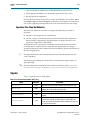
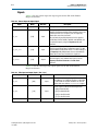
Table 1–1 lists the features of the SDI MegaCore function.
Table 1–1. SDI MegaCore Function Features
Feature
Description
■
Multiple SDI standards and video formats (refer to Table 1–5 and Table 1–6)
■
RP168 video switch line requirement
■
OpenCore Plus evaluation
■
Cyclical redundancy check (CRC) encoding (HD only)
■
Line number (LN) insertion (HD only)
■
Word scrambling
■
Transmitter clock multiplexer (optional)
■
CRC decoding (HD only)
■
LN extraction (HD only)
■
Framing and extraction of video timing signals
■
Word alignment and descrambling
MegaWizard™ Plug-In Manager
■
Easy-to-use parameter editor
IP functional simulation models
■
Support
Transmitter
Receiver
February 2013
Altera Corporation
Use in Altera-supported VHDL and Verilog HDL simulators
Serial Digital Interface (SDI) MegaCore Function
User Guide
1–2
Chapter 1: About This MegaCore Function
Release Information
Release Information
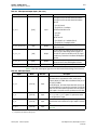
Table 1–2 lists information about this release of the SDI MegaCore function.
Table 1–2. Release Information
Item
Description
Version
12.1
Release Date
January 2013
Ordering Code
IP-SDI
00AE (SDI MegaCore function)
Product ID(s)
00EF (SDI Audio cores)
Vendor ID
6AF7
f For more information about this release, refer to the MegaCore IP Library Release Notes
and Errata.
Altera verifies that the current version of the Quartus® II software compiles the
previous version of each MegaCore function. The MegaCore IP Library Release Notes
and Errata report any exceptions to this verification. Altera does not verify
compilation with MegaCore function versions older than one release.
Device Family Support
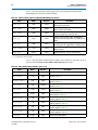
Table 1–3 defines the device support levels for Altera IP cores.
Table 1–3. Altera IP Core Device Support Levels
FPGA Device Families
HardCopy Device Families
Preliminary support—The IP core is verified with
preliminary timing models for this device family. The IP core
meets all functional requirements, but might still be
undergoing timing analysis for the device family. It can be
used in production designs with caution.
HardCopy Companion—The IP core is verified with
preliminary timing models for the HardCopy companion
device. The IP core meets all functional requirements, but
might still be undergoing timing analysis for the HardCopy
device family. It can be used in production designs with
caution.
Final support—The IP core is verified with final timing
models for this device family. The IP core meets all
functional and timing requirements for the device family and
can be used in production designs.
HardCopy Compilation—The IP core is verified with final
timing models for the HardCopy device family. The IP core
meets all functional and timing requirements for the device
family and can be used in production designs.
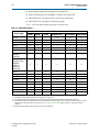
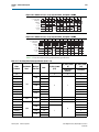
Table 1–4 shows the level of support offered by the SDI MegaCore function for each
Altera device family.
Table 1–4. Device Family Support (Part 1 of 2)
Serial Digital Interface (SDI) MegaCore Function
User Guide
Device Family
Support
Arria® GX
Final
Arria II (1)
Final
Arria V
Refer to the What’s New in Altera IP page of
the Altera website.
February 2013 Altera Corporation
Chapter 1: About This MegaCore Function
General Description
1–3
Table 1–4. Device Family Support (Part 2 of 2)
Device Family
Support
Cyclone®
Final (3)
Cyclone II (2)
Final
Cyclone III (2)
Final
Cyclone III LS (2)
Final
Cyclone IV GX (4)
Final
Cyclone V (5)
Refer to the What’s New in Altera IP page of
the Altera website.
HardCopy® III/ IV E
HardCopy Compilation
HardCopy IV GX
HardCopy Compilation
Stratix®
(2)
Final
Stratix GX
Final
Stratix II (2)
Final
Stratix II GX
Final
Stratix III (2)
Final
Stratix IV (1)
Final
Stratix V (1)
Refer to the What’s New in Altera IP page of
the Altera website.
Other device families
No support
Notes to Table 1–4:
(1) If you have only 27 MHz to drive the SDI MegaCore function in SD-SDI mode, you require an additional PLL to
generate a 67.5-MHz reference clock.
(2) The Cyclone series of devices, and Stratix, Stratix II, and Stratix III devices only support soft
serializer /deserializer (SERDES).
(3) Cyclone device support is limited to –6 speed grade devices.
(4) Transceiver dynamic configuration with channel reconfiguration mode is not supported for dual and triple standard
in EP4CGX110 and EP4CGX150 devices. Use transceiver dynamic reconfiguration with PLL reconfiguration mode
instead.
(5) The Cyclone V devices does not support the SDI Audio IP cores.
General Description
The Society of Motion Picture and Television Engineers (SMPTE) have defined an SDI
that video system designers use widely as an interconnect between equipment in
video production facilities.
The SDI MegaCore function can handle the following SDI data rates:
February 2013
■
270 megabits per second (Mbps) SD-SDI, as defined by SMPTE259M-1997 10-Bit
4:2:2 Component Serial Digital Interface
■
1.5-Gbps HD-SDI, as defined by SMPTE292M-1998 Bit-Serial Digital Interface for
High Definition Television Systems
■
3-Gbps SDI, as defined by SMPTE425M-AB 2006 3Gb/s Signal/Data Serial Interface–
Source Image Format Mapping
■
Preliminary support for dual link SDI, as defined by SMPTE372M-Dual Link
1.5Gb/s Digital Interface for 1920×1080 and 2048×1080 Picture Formats
Altera Corporation
Serial Digital Interface (SDI) MegaCore Function
User Guide
1–4
Chapter 1: About This MegaCore Function
General Description
■
Dual standard support for 270-Mbps and 1.5-Gbps SDI
■
Triple standard support for 270-Mbps, 1.5-Gbps, and 3-Gbps SDI
■
SMPTE425M Level A support (direct source image formatting)
■
SMPTE425M Level B support (dual link mapping)
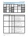
Table 1–5 lists the SDI standard support for various devices.
Table 1–5. SDI Standard Support
(1)
SDI Standard
Device Family
(2)
Dual Standard
Triple Standard
v
v
v
v
v
v
v
v
v
v
v
v
v
—
—
—
—
—
Cyclone II
v
—
—
—
—
—
Cyclone III
v
—
—
—
—
—
Cyclone IV GX
(EP4CGX15,
EP4CGX30)
v
—
—
—
—
—
SD-SDI
HD-SDI
3G-SDI
Arria GX
v
v
v
Arria II GX
v
v
Arria V
v
Cyclone
HD-SDI Dual Link
Cyclone IV GX
(EP4CGX30 (F484),
EP4CGX50,
EP4CGX75,
EP4CGX110,
EP4CGX150)
v
v
v
v
v
v
Cyclone V (3)
v
v
v
v
v
v
HardCopy IV GX
v
v
v
v
v
v
Stratix
v
—
—
—
—
—
Stratix GX
v
v
—
v
v
—
Stratix II
v
—
—
—
—
—
Stratix II GX
v
v
v
v
v
v
Stratix III
v
—
—
—
—
—
IV (4)
v
v
v
v
v
v
Stratix V (4)
v
v
v
v
v
v
Stratix
Notes to Table 1–5:
(1) All standards, other than SD-SDI, require a transceiver based or “GX” device.
(2) The HD-SDI dual link supports timing difference up to 40 ns between link A and link B, fulfilling the SMPTE372M requirement.
(3) The 3G-SDI standard is not supported in Cyclone V devices with transceiver speed grade 7, due to the excessive data rate required. For more
information about the Cyclone V device, refer to the Overview for Cyclone V Device Family chapter in volume 1 of the Cyclone V Device
Handbook.
(4) Only Stratix IV and Stratix V variants with transceivers support all SDI rates.
Serial Digital Interface (SDI) MegaCore Function
User Guide
February 2013 Altera Corporation
Chapter 1: About This MegaCore Function
General Description
1–5
Table 1–6 lists the HD-SDI standard video format specification.
Table 1–6. HD-SDI Video Format Specification
SMPTE292M
274M
296M
Video Format
1920 x 1080
1280 x 720
(1) (2)
Sample per
Active Line
1920
1280
Active Line
per Frame
1080
720
260M
1920 x 1035
1920
1035
295M
1920 x 1080
1920
1080
Sample per
Total Line
Total Line
per Frame
Frame Rate
SDI 11.1
Support
2200
1125
60
Yes
2640
1125
50
Yes
2200
1125
30
Yes
2640
1125
25
Yes
2750
1125
24
Yes
1650
750
60
Yes
1980
750
50
Yes
3300
750
30
Yes
3960
750
25
Yes
4125
750
24
Yes
2200
1125
30
Yes
2376
1250
25
Yes
2376
1250
50
Yes
Notes to Table 1–6:
(1) The video formats support 4:2:2(YC’BC’R)/10-bit, 4:4:4(RGB)/(YC’BC’R), 4:4:4:4 (RGB+A)/(YC’BC’R+A)/10-bit, 4:4:4(YC’BC’R)/12-bit,
4:4:4(RGB)/12-bit, and 4:2:2 (YC’BC’R)/12-bit mapping structures.
(2) 3G-SDI is similar to HD-SDI except the data bit rate is twice that of HD-SDI or approximately 3 Gbps.
OpenCore Plus Evaluation
With Altera’s free OpenCore Plus evaluation feature, you can perform the following
actions:
■
Simulate the behavior of a megafunction (Altera MegaCore function or AMPPSM
megafunction) within your system.
■
Verify the functionality of your design and quickly evaluate its size and speed
with ease.
■
Generate time-limited device programming files for designs that include
MegaCore functions.
■
Program a device and verify your design in hardware.
You are required to obtain a license for the MegaCore function only when you are
completely satisfied with its functionality and performance, and want to take your
design to production.
f For more information about OpenCore Plus hardware evaluation using the SDI, refer
to “OpenCore Plus Time-Out Behavior” on page 3–39 and AN 320: OpenCore Plus
Evaluation of Megafunctions.
February 2013
Altera Corporation
Serial Digital Interface (SDI) MegaCore Function
User Guide
1–6
Chapter 1: About This MegaCore Function
Resource Utilization
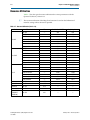
Resource Utilization
Table 1–7 lists the typical resource utilization for various parameters with the
Quartus II software, version 11.1.
1
The resource utilization of the MegaCore function is based on the bidirectional
interface settings unless otherwise specified.
Table 1–7. Resource Utilization (Part 1 of 2)
Device
Arria GX
Arria II GX
Arria V
Video Standard
LEs
Combinational ALUTs
Logic Registers
SD-SDI
—
834
640
HD-SDI
—
919
683
3G-SDI
—
1,161
865
Dual link HD-SDI
—
1,906
1,423
Dual standard receiver
—
1,188
831
Dual standard transmitter
—
247
185
Triple standard
—
1,794
1,215
SD-SDI
—
839
680
HD-SDI
—
978
833
3G HD-SDI
—
1,259
1,015
Dual-Link HD-SDI
—
2,029
1,711
Dual standard receiver
—
1,257
926
Dual standard transmitter
—
267
180
Triple standard
—
1,891
1,305
SD-SDI
—
1,189
920
HD-SDI
—
1,185
910
3G-SDI
—
1,444
1,142
Dual link HD-SDI
—
2,446
1,880
Dual standard receiver
—
1,605
1,175
Dual standard transmitter
—
349
269
Triple standard
—
2,273
1,677
Cyclone
SD-SDI
875
—
—
Cyclone II
SD-SDI
867
—
—
Cyclone III
SD-SDI
874
—
—
Cyclone III LS
SD-SDI
929
—
—
Cyclone IV GX
(EP4CGX15,
EP4CGX30)
SD-SDI
916
—
—
Serial Digital Interface (SDI) MegaCore Function
User Guide
February 2013 Altera Corporation
Chapter 1: About This MegaCore Function
Resource Utilization
1–7
Table 1–7. Resource Utilization (Part 2 of 2)
Device
Video Standard
Cyclone IV GX
(EP4CGX50,
EP4CGX75,
EP4CGX110, and
EP4CGX150)
LEs
Combinational ALUTs
Logic Registers
SD-SDI
—
1,129
671
HD-SDI
—
1,164
670
3G-SDI
—
1,409
790
Dual link HD-SDI
—
2,515
1,467
Dual standard receiver
—
1,479
755
Dual standard transmitter
—
364
229
Triple standard
—
2,235
1,121
SD-SDI
—
1,140
832
HD-SDI
—
1,122
808
3G-SDI
—
1,402
997
Dual link HD-SDI
—
2,351
1,696
Dual standard receiver
—
1,539
1,042
Dual standard transmitter
—
352
260
Triple standard
—
2,217
1,508
Stratix
SD-SDI
875
—
—
Stratix II
SD-SDI
—
581
533
Stratix III
SD-SDI
—
602
565
SD-SDI
1,182
—
—
HD-SDI
1,316
—
—
Dual link HD-SDI
2,703
—
—
Dual standard
1,819
—
—
SD-SDI
—
834
640
HD-SDI
—
919
683
3G-SDI
—
1,161
865
Dual link HD-SDI
—
1,906
1,423
Dual standard receiver
—
1,188
831
Cyclone V
Stratix GX
Stratix II GX
Stratix IV GX
Stratix V
February 2013
Dual standard transmitter
—
247
185
Triple standard
—
1,794
1,215
SD-SDI
—
839
680
HD-SDI
—
978
833
3G-SDI
—
1,259
1,015
Dual link HD-SDI
—
2,029
1,711
Dual standard receiver
—
1,257
926
Dual standard transmitter
—
267
180
Triple standard
—
1,891
1,305
SD-SDI
—
913
707
HD-SDI
—
955
703
3G-SDI
—
1,126
823
Dual link HD-SDI
—
2,049
1,522
Altera Corporation
Serial Digital Interface (SDI) MegaCore Function
User Guide
1–8
Serial Digital Interface (SDI) MegaCore Function
User Guide
Chapter 1: About This MegaCore Function
Resource Utilization
February 2013 Altera Corporation
2. Getting Started
Design Flow
To evaluate the SDI MegaCore function using the OpenCore Plus feature, follow these
steps in your design flow:
1. Obtain and install the SDI MegaCore function.
The SDI MegaCore function is part of the MegaCore IP Library, which is
distributed with the Quartus II software and downloadable from the Altera
website at www.altera.com.
f For system requirements and installation instructions, refer to Altera
Software Installation & Licensing.
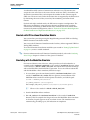
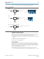
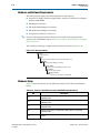
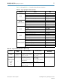
Figure 2–1 shows the directory structure after you install the SDI MegaCore function,
where <path> is the installation directory. The default installation directory on
Windows is c:\altera\<version>; on Linux, it is /opt/altera<version>.
February 2013
Altera Corporation
Serial Digital Interface (SDI) MegaCore Function
User Guide
2–2
Chapter 2: Getting Started
Design Flow
Figure 2–1. Directory Structure
<path>
Installation directory.
ip
Contains the Altera MegaCore IP Library and third-party IP cores.
altera
Contains the Altera MegaCore IP Library.
common
Contains shared components.
sdi
Contains the SDI MegaCore function files.
example
Contains design examples.
a2gx_tr
Contains a design example for Arria II GX.
s2gx_tr
Contains a design example for Stratix II GX, see AN 339: Serial
lib Digital Interface Demonstration for Stratix II GX Devices.
Contains encrypted lower-level design files and other support files.
simulation
Contains simulation files.
hdsdi
Contains the HD-SDI simulation files.
quartus
Contains the Quartus II NativeLink project.
testbench
Contains the testbench files.
pattern_gen
Contains the pattern generator files for the testbench.
hdsdi_3g
Contains the HD-SDI 3 Gbps simulation files.
quartus
Contains the Quartus II NativeLink project.
testbench
Contains the testbench files.
pattern_gen
Contains the pattern generator files for the testbench.
hdsdi_dual_link
Contains the HD-SDI dual link simulation files.
quartus
Contains the Quartus II NativeLink project.
testbench
Contains the testbench files.
pattern_gen
Contains the pattern generator files for the testbench.
modelsim
Contains the ModelSim simulation files.
1. Create a custom variation of the SDI MegaCore function.
2. Implement the rest of your design using the design entry method of your choice.
3. Use the IP functional simulation model to verify the operation of your design.
f For more information on IP functional simulation models, refer to the
Simulating Altera Designs chapter in volume 3 of the Quartus II Handbook.
Serial Digital Interface (SDI) MegaCore Function
User Guide
February 2013 Altera Corporation
Chapter 2: Getting Started
SDI Walkthrough
2–3
4. Use the Quartus II software to compile your design.
1
You can also generate an OpenCore Plus time-limited programming file,
which you can use to verify the operation of your design in hardware.
5. Purchase a license for the SDI MegaCore function.
After you have purchased a license for the SDI MegaCore function, follow these
additional steps:
1. Set up licensing.
2. Generate a programming file for the Altera device or devices on your board.
3. Program the Altera device or devices with the completed design.
SDI Walkthrough
This walkthrough explains how to create an SDI design using the MegaWizard
Plug-In Manager and the Quartus II software. After you generate a custom variation
of the SDI MegaCore function, you can incorporate it into your overall project.
1
You can alternatively use the IP Advisor to help start your SDI MegaCore design. On
the Quartus II Tools menu, point to Advisors, and then click IP Advisor. The IP
Advisor guides you through a series of recommendations for selecting,
parameterizing, evaluating, and instantiating an SDI MegaCore function into your
design. It then guides you through a complete Quartus II compilation of your project.
This walkthrough requires the following steps:
1. “Creating a New Quartus II Project”
2. “Launching MegaWizard Plug-In Manager”
3. “Parameterizing”
4. “Setting Up Simulation”
5. “Generating Files”
Creating a New Quartus II Project
You must create a new Quartus II project with the New Project Wizard, which
specifies the working directory for the project, assigns the project name, and
designates the name of the top-level design entity. To create a new project, follow
these steps:
1. Choose Programs > Altera > Quartus II <version> (Windows Start menu) to run
the Quartus II software. Alternatively, you can use the Quartus II Web Edition
software.
2. On the File menu, click New Project Wizard.
3. Click Next in the New Project Wizard: Introduction page (the introduction page
does not display if you turned it off previously).
February 2013
Altera Corporation
Serial Digital Interface (SDI) MegaCore Function
User Guide
2–4
Chapter 2: Getting Started
SDI Walkthrough
4. In the New Project Wizard: Directory, Name, Top-Level Entity page, enter the
following information:
a. Specify the working directory for your project. For example, this walkthrough
uses the c:\altera\projects\sdi_project directory.
1
The Quartus II software automatically specifies a top-level design entity
that has the same name as the project. This walkthrough assumes that the
names are the same.
b. Specify the name of the project. This walkthrough uses project for the project
name.
5. Click Next to close this page and display the New Project Wizard: Add Files page.
1
When you specify a directory that does not already exist, a message
prompts you to create a specified directory. Click Yes to create the directory.
6. If you installed the MegaCore IP Library in a different directory from where you
installed the Quartus II software, you must add the user libraries:
a. Click User Libraries.
b. Type <path>\ip into the Library name field, where <path> is the directory in
which you installed the SDI.
c. Click Add to add the path to the Quartus II project.
d. Click OK to save the library path in the project.
7. Click Next to close this page and display the New Project Wizard: Family &
Device Settings page.
8. On the New Project Wizard: Family & Device Settings page, choose the target
device family in the Family list.
9. The remaining pages in the New Project Wizard are optional. Click Finish to
complete the Quartus II project.
Launching MegaWizard Plug-In Manager
To launch the MegaWizard Plug-In Manager in the Quartus II software, follow these
steps:
1. On the Tools menu, click MegaWizard Plug-In Manager.
1
For more information about how to use the MegaWizard Plug-In Manager,
refer to Quartus II Help.
2. Specify that you want to create a new custom megafunction variation and click
Next.
3. Expand the Interfaces > SDI folder and click SDI <version>.
4. Select the output file type for your design; the wizard supports VHDL and Verilog
HDL.
Serial Digital Interface (SDI) MegaCore Function
User Guide
February 2013 Altera Corporation
Chapter 2: Getting Started
SDI Walkthrough
2–5
5. The MegaWizard Plug-In Manager shows the project path that you specified in the
New Project Wizard. Append a variation name for the MegaCore function output
files <project path>\<variation name>.
6. Click Next to display the Parameter Settings page for the SDI MegaCore function.
1
You can change the page that the MegaWizard Plug-In Manager displays by
clicking Next or Back at the bottom of the dialog box. You can move
directly to a named page by clicking the Parameter Settings, EDA, or
Summary tab.
Also, you can directly display individual parameter settings by clicking on
the Protocol Options, Transceiver Options, or Receiver/Transmitter
Options tab.
Parameterizing
To parameterize your MegaCore function, follow these steps:
1. Select the video standard. Some of the standards may be grayed out, because they
are not supported on the currently selected device family.
2. Select Bidirectional, Receiver, or Transmitter interface direction.
3. Click the Transceiver Options tab.
4. Under Transceiver and Protocol, click Generate transceiver and protocol blocks.
5. For SD-SDI only, turn on Use soft logic for transceiver to implement the
transceiver in logic, rather than using Stratix GX, Stratix II GX or Stratix IV GX
transceivers.
6. Select the starting channel number.
7. Turn on Use PLL reconfiguration for transceiver dynamic reconfiguration if you
select an EP4CGX110 or EP4CGX150 device for Cyclone IV GX using dual and
triple standards. You may turn on this option for other Cyclone IV GX devices but
it is not recommended.
8. Turn on Enable TX PLL select for 1/1.000 and 1/1.001 data rate reconfiguration if
your design requires two serial input clocks to the TX block.
1
This feature is only available for the Arria II, Stratix IV GX, and
HardCopy IV GX device families.
9. Click the Receiver/Transmitter Options tab.
10. Turn on the required receiver options.
11. Turn on the required transmitter options.
12. Click Next (or the EDA tab) to display the EDA page.
f For more information about parameters, refer to “Parameters” on page 3–56 and, for
more information about the protocol options, refer to Table 3–20 on page 3–56.
For more information about the transceiver options, refer to Table 3–21 on page 3–56.
For more information about the receiver/transmitter options, refer to Table 3–22 on
page 3–57.
February 2013
Altera Corporation
Serial Digital Interface (SDI) MegaCore Function
User Guide
2–6
Chapter 2: Getting Started
SDI Walkthrough
Setting Up Simulation
An IP functional simulation model is a cycle-accurate VHDL or Verilog HDL model
produced by the Quartus II software. The model allows for fast functional simulation
of IP using industry-standard VHDL and Verilog HDL simulators.
c You may only use these models for simulation and expressly not for synthesis or any
other purposes. Using these models for synthesis creates a nonfunctional design.
To generate an IP functional simulation model for your MegaCore function, follow
these steps:
1. Turn on Generate simulation model.
2. Some third-party synthesis tools can use a netlist that contains only the structure
of the MegaCore function, but not detailed logic, to optimize performance of the
design that contains the MegaCore function. If your synthesis tool supports this
feature, turn on Generate netlist.
3. Click Next (or the Summary tab) to display the Summary page.
Generating Files
You can use the check boxes on the Summary page to enable or disable the generation
of specified files. A gray checkmark indicates a file that is automatically generated; a
red checkmark indicates an optional file.
You can click Back to display the previous page, or click Parameters Settings, EDA,
or Summary, to change any of the MegaWizard options.
To generate the files, follow these steps:
1. Turn on the files you wish to generate.
1
At this stage, you can still click Back to display any of the other pages in the
MegaWizard Plug-In Manager to change any of the parameters.
2. To generate the specified files and close the MegaWizard Plug-In Manager, click
Finish.
1
The generation phase may take several minutes to complete.
1
The Quartus II IP File (.qip) is a file generated by the parameter editor, and
contains information about the generated IP core. You are prompted to add
this .qip file to the current Quartus II project at the time of file generation.
In most cases, the .qip file contains all of the necessary assignments and
information required to process the core or system in the Quartus II
compiler. Generally, a single .qip file is generated for each MegaCore
function or system in the Quartus II compiler.
3. Click Exit to close the Generation window.
Serial Digital Interface (SDI) MegaCore Function
User Guide
February 2013 Altera Corporation
Chapter 2: Getting Started
SDI Walkthrough
2–7
Table 2–1 describes the generated files and other files that may be in your project
directory. The names and types of files specified in the MegaWizard Plug-In Manager
report vary based on whether you created your design with VHDL or Verilog HDL.
Table 2–1. Generated Files
Extension
Description
<variation name>.v or .vhd
A MegaCore function variation file, which defines a VHDL or Verilog HDL description of
the custom MegaCore function. Instantiate the entity defined by this file inside of your
design. Include this file when compiling your design in the Quartus II software.
<variation name>.cmp
A VHDL component declaration file for the MegaCore function variation. Add the
contents of this file to any VHDL architecture that instantiates the MegaCore function.
<variation name>.bsf
Quartus II symbol file for the MegaCore function variation. You can use this file in the
Quartus II block diagram editor.
<variation name>.html
MegaCore function report file.
<variation name>.ppf
This XML file describes the MegaCore pin attributes to the Quartus II Pin Planner.
MegaCore pin attributes include pin direction, location, I/O standard assignments, and
drive strength. If you launch IP Toolbench outside of the Pin Planner application, you
must explicitly load this file to use Pin Planner.
<variation name>_sdi.sdc
Contains timing constraints for your SDI variation.
Quartus II file that sets the Quartus II to use TimeQuest timing analyzer and patches the
generated .sdc script with a new clock name. If your top-level design clock pin names do
<variation name>_constraints.tcl
not match the default clock pin names or a prefixed version, edit the assignments in this
file.
<variation name>.vo or .vho
VHDL or Verilog HDL IP functional simulation model.
<variation name>_bb.v
A Verilog HDL black-box file for the MegaCore function variation. Use this file when
using a third-party EDA tool to synthesize your design.
<variation name>.qip
Contains Quartus II project information for your MegaCore function variations.
You can now integrate your custom MegaCore function variation into your design,
simulate, and compile.
February 2013
Altera Corporation
Serial Digital Interface (SDI) MegaCore Function
User Guide
2–8
Chapter 2: Getting Started
Simulating the Design
Simulating the Design
This section describes the following simulation techniques:
■
Simulate with IP Functional Simulation Models
■
Simulating with the ModelSim Simulator
■
Simulating in Third-Party Simulation Tools Using NativeLink
Testbench
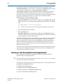
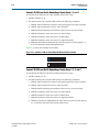
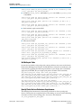
In general, all testbenches are constructed in such a way that the serial transmit data is
looped back to receiver. Figure 2–2 shows how the serial transmit data is looped back
to the receiver in the testbench.
Figure 2–2. General Simulation Testbench
SDI RECEIVE TEST
Transmitter TRS
Counter
Transmitter Data
Descrambler
SDI Pattern Generator
SDI IP CORE - Transmitter
- SD 270 Mbps
- HD 1.485 Gbps
- 3G 2.97 Gbps
SDI TRANSMIT TEST
ALTGXB
RECONFIG (1)
Receiver TRS
Checker
SDI IP CORE - Receiver
Receiver Lock
Checker
Receiver Line
Checker
DUT
Note to Figure 2–2:
(1) For dual or triple standard only.
Serial Digital Interface (SDI) MegaCore Function
User Guide
February 2013 Altera Corporation
Chapter 2: Getting Started
Simulating the Design
2–9
A testbench basically consists of transmit test and receive test. The transmit test
accepts the same serial data as the receive device under test (DUT), deserializes and
decodes the transmitted data, and computes the number of time reference signals
(TRS) seen. The receive test verifies the features that are supported by the SDI receiver
by monitoring the received data, status bits, line numbering and other related
features.
For dual and triple standard modes, the SDI receiver requires reconfiguration. The
SDI receiver reconfigures using transceiver dynamic reconfiguration to perform
autodetection and locking to different SDI video standards. For more details about
transceiver dynamic reconfiguration, refer to “Transceiver Dynamic Reconfiguration
for Dual Standard and Triple Standard Receivers” on page 3–27.
Simulate with IP Functional Simulation Models
You can simulate your design using the MegaWizard-generated VHDL and Verilog
HDL IP functional simulation models.
You can use the IP functional simulation model with any Altera-supported VHDL or
Verilog HDL simulator.
To use the IP functional simulation model that you created in “Setting Up Simulation”
on page 2–6, create a suitable testbench.
f For more information about IP functional simulation models, refer to the Simulating
Altera Designs chapter in volume 3 of the Quartus II Handbook.
Simulating with the ModelSim Simulator
For Arria and Stratix series of devices, Altera provides two fixed testbenches as
examples in the simulation\modelsim\<video standard>\modelsim directory, where
<video standard> is hdsdi or hdsdi_dual_link. The testbenches instantiate the design
and test the HD-SDI or dual link mode of operation. To use one of these testbenches
with the ModelSim®-Altera simulator, follow these steps:
1. In a text editor, open the simulation batch file, simulation\modelsim\<video
standard>\modelsim\sdi_sim.bat. Edit it to point to your installation of the
ModelSim-Altera simulator and the Quartus II software, and edit the path:
set PATH = %MODELSIM_DIR%\win32aloem
set QUARTUS_ROOTDIR=c:\altera\81\quartus
For example, edit QUARTUS_ROOTDIR=/tools/acds/11.0/157/linux32/quartus.
1
Where <video standard> is hdsdi or hdsdi_dual_link.
2. Start the ModelSim-Altera simulator.
3. Run sdi_sim.bat in the simulation\modelsim\<video standard>\modelsim
directory. This file compiles the design and starts the ModelSim-Altera simulator.
A selection of signals appears on the waveform viewer. The simulation runs
automatically, providing a pass/fail indication on completion.
February 2013
Altera Corporation
Serial Digital Interface (SDI) MegaCore Function
User Guide
2–10
Chapter 2: Getting Started
Simulating the Design
For Cyclone IV GX devices, Altera provides two new fixed testbenches in the
simulation\modelsim\<video standard>\<DPRIO mode>\modelsim directory, where
<video standard>\<DPRIO mode> is trsdi_c4gx\channel_reconfig or
trsdi_c4gx\pll_reconfig. The testbenches instantiate the design and test the triple
standard mode of operation using Cyclone IV GX devices. The testbenches also
demonstrate the transceiver dynamic reconfiguration with channel and phase-locked
loop (PLL) reconfiguration modes. To use one of these testbenches with the
ModelSim-Altera simulator, follow these steps:
1. In a text editor, open the simulation .do file,
simulation\modelsim\<video standard>\<DPRIO mode>\modelsim\sdi_sim.do.
Edit it to point to your installation of the ModelSim-Altera simulator, and edit the
path:
set QUARTUS_ROOTDIR = C:\altera\<version>\quartus
1
Where <version> is the version of the Quartus II software you are using.
2. Start the ModelSim-Altera simulator.
3. Run sdi_sim.do in the
simulation\modelsim\<video standard>\<DPRIO mode>\modelsim directory.
This file compiles the design and starts the ModelSim-Altera simulator. A selection
of signals appears on the waveform viewer.
To test the transmitter operation, the testbench generates a reference clock and parallel
video data. The design encodes and serializes this parallel video data. The serial
output is sampled, non-return to zero inverted (NRZI) decoded, descrambled, and
then reconstructed into parallel form. The testbench detects the presence of TRS
tokens (end of active video (EAV) and start of active video (SAV)) in the output to
check the correct operation.
To test the receiver operation, the testbench connects the serial transmitter data to the
receiver input. The testbench checks that the receiver achieves word alignment and
verifies that the extracted LN is correct.
Simulating in Third-Party Simulation Tools Using NativeLink
You can perform a simulation in a third-party simulation tool from within the
Quartus II software, using NativeLink.
f For more information about NativeLink, refer to the Simulating Altera Designs chapter
in volume 3 of the Quartus II Handbook.
Altera provides the following three Quartus II projects for use with NativeLink in the
ip\altera\sdi\simulation directory:
■
HD-SDI in the hdsdi directory
■
HD-SDI 3 Gbps in the hdsdi_3g directory
■
HD-SDI dual link in the hdsdi_dual_link directory
■
Triple standard SDI in the trsdi directory
Serial Digital Interface (SDI) MegaCore Function
User Guide
February 2013 Altera Corporation
Chapter 2: Getting Started
Specifying Constraints
2–11
To set up simulation in the Quartus II software using NativeLink, follow these steps:
1. On the File menu, click Open Project. Browse to the desired directory: hdsdi,
hdsdi_3g, hdsdi_dual_link, or trsdi.
2. Open sdi_sim.qpf.
3. Check that the absolute path to your third-party simulator executable is set. On the
Tools menu, click Options and select EDA Tools Options.
4. On the Processing menu, point to Start and click Start Analysis & Elaboration.
5. On the Tools menu, point to Run EDA Simulation Tool and click EDA RTL
Simulation.
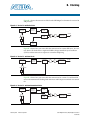
Specifying Constraints
You must apply the Altera-provided timing constraint file in Synopsys Design
Constraints File (.sdc) format and the additional Tcl Script File (.tcl) to ensure the SDI
MegaCore function meets the design timing requirements.
To add the .sdc file to your project, click Add/Remove Files in Project on the Project
menu and browse to select <variation name>_sdi.sdc file.
To add the additional .tcl file, you must compile your design and perform post
compilation timing analysis using the TimeQuest timing analyzer. On the
Assignments menu, click Use TimeQuest Timing Analyzer during compilation, and
click OK.
You may have to further edit your scripts if your design requires single channel or
multiple channels.
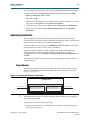
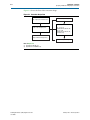
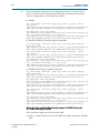
Single Channel
The following section describes what you must do if your design requires a single
channel using SDI triple standard transmitter and receiver instances as shown in
Figure 2–3 on page 2–11.
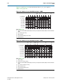
Figure 2–3. Instantiating Single Channel of SDI Instances
SYSTEM TOP LEVEL
Transceiver Bank 1
tx_serial_refclk_top1
1
SDI triple standard transmitter
starting_channel_number = 0
SDI triple standard receiver
starting_channel_number = 4
rx_serial_refclk_top1
The SDI instances must have a unique starting channel number if they are merged
into a same quad or bank.
To specify the constraints, follow these steps:
1. Parameterize and generate your SDI MegaCore functions—SDI triple standard
transmitter and receiver.
February 2013
Altera Corporation
Serial Digital Interface (SDI) MegaCore Function
User Guide
2–12
Chapter 2: Getting Started
Specifying Constraints
2. Edit the Tcl script so that the transceiver top-level reference clock matches the
clock pin names that you have chosen for your design, for example
tx_serial_refclk_top1. Locate tx_serial_refclk_name in the script and change
to tx_serial_refclk_top1.
1
The SDI triple standard transmitter has a transceiver top-level reference
clock, tx_serial_refclk.
3. Execute the Tcl script to patch the generated .sdc script with the new clock names.
1
A back-up copy of the .sdc script is created before the patch is made, and
any edits that were previously made to the .sdc script are preserved.
4. Execute the Tcl script in the Quartus II software, and follow these steps:
a. On the Tools menu, click Tcl script.
b. Select the Tcl script of the instance SDI triple standard transmitter, and click
Run.
5. Perform steps 2 to 4 for the SDI triple standard receiver instance.
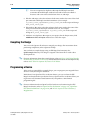
Multiple Channels
The following section describes what you must do if your design requires multiple
channels using four instances of SDI triple standard transmitter and four instances of
SDI triple standard receiver. In this case, assume that you must fit all instances into
Transceiver Bank 1 and 2 as shown in Figure 2–4, and the SDI instances in both banks
have the same video standard. You do not have to regenerate the SDI instances in
Transceiver Bank 2.
Figure 2–4. Instantiating Multiple Channels of SDI Instances Sharing Same Reference Clock
SYSTEM TOP LEVEL
Transceiver Bank 1
tx_serial_refclk_top1
SDI triple standard transmitter A
starting_channel_number = 0
SDI triple standard receiver A
starting_channel_number = 4
SDI triple standard transmitter B
starting_channel_number = 8
SDI triple standard receiver B
starting_channel_number = 12
rx_serial_refclk_top1
Transceiver Bank 2
SDI triple standard transmitter A
starting_channel_number = 0
SDI triple standard receiver A
starting_channel_number = 4
SDI triple standard transmitter B
starting_channel_number = 8
SDI triple standard receiver B
starting_channel_number = 12
Serial Digital Interface (SDI) MegaCore Function
User Guide
February 2013 Altera Corporation
Chapter 2: Getting Started
Specifying Constraints
2–13
To specify the constraints, perform the following steps:
1. Parameterize and generate your SDI MegaCore functions—SDI triple standard
transmitter A, SDI triple standard transmitter B, SDI triple standard receiver A,
and SDI triple standard receiver B—with their unique starting channel number.
2. Edit the Tcl script so that the transceiver top-level reference clock matches the
name of the clock pin connected to SDI triple standard transmitter A, for example
tx_serial_refclk_top1. Locate tx_serial_refclk_name in the script and change
to tx_serial_refclk_top1.
3. Execute the Tcl script to patch the generated .sdc script with the new clock names.
1
A back-up copy of the .sdc script is created before the patch is made, and
any edits that were previously made to the .sdc script are preserved.
4. Execute the Tcl script in the Quartus II software, and perform the following steps:
a. On the Tools menu, click Tcl script.
b. Select the Tcl script of the instance SDI triple standard transmitter A, and click
Run.
5. Perform steps 2 to 4 for the other three instances.
Figure 2–5. Instantiating Multiple Channels of SDI Instances Sharing Multiple Reference Clocks
SYSTEM TOP LEVEL
Transceiver Bank 1
tx_serial_refclk_top1
SDI triple standard transmitter A
starting_channel_number = 0
SDI triple standard receiver A
starting_channel_number = 4
SDI triple standard transmitter B
starting_channel_number = 8
SDI triple standard receiver B
starting_channel_number = 12
rx_serial_refclk_top1
Transceiver Bank 2
tx_serial_refclk_top2
SDI triple standard transmitter A
starting_channel_number = 0
SDI triple standard receiver A
starting_channel_number = 4
SDI triple standard transmitter B
starting_channel_number = 8
SDI triple standard receiver B
starting_channel_number = 12
rx_serial_refclk_top2
To specify constraints for multiple channels of SDI MegaCore function with multiple
top-level reference clocks as shown in Figure 2–5, perform the following steps:
1. For the SDI instances in Transceiver Bank 1, perform steps 1 to 5 you would do for
SDI instances sharing the same reference clock.
2. For the SDI instances in Transceiver Bank 2, duplicate an .sdc script for SDI triple
standard transmitter A and SDI triple standard receiver A in Transceiver Bank 2.
February 2013
Altera Corporation
Serial Digital Interface (SDI) MegaCore Function
User Guide
2–14
Chapter 2: Getting Started
Compiling the Design
1
You are not required to duplicate .sdc script for SDI triple standard
transmitter B and SDI triple standard receiver B in Transceiver Bank 2.
Instances with same video standard can share an .sdc script.
3. Edit the .sdc script so that the reference clock name matches the name of the clock
pin connected to SDI triple standard transmitter A, for example
tx_serial_refclk_top2. Locate tx_serial_refclk_name in the script and change
to tx_serial_refclk_top2.
4. Edit another .sdc script so that the reference clock name matches the name of the
clock pin connected to SDI triple standard receiver A, for example
rx_serial_refclk_top2. Locate set rx_serial_refclk_name in the script and
change to rx_serial_refclk_top2.
5. Add these two duplicate .sdc scripts to your project. On the Project menu, click
Add/Remove Files in Project and browse to select the scripts.
Compiling the Design
You can use the Quartus II software to compile your design. For instructions about
performing compilation, refer to Quartus II Help.
You can find an example design using an SDI MegaCore function in the
ip/sdi/example directory. This design is targeted at the Stratix II GX audio video
development kit.
f For more information about the example design, refer to AN 339: Serial Digital Interface
Demonstration for Stratix II GX Devices, and for information about the development kit,
refer to Audio Video Development Kit, Stratix II GX Edition.
Programming a Device
After you have compiled the example design, you can program your targeted Altera
device to verify the design in hardware.
With Altera's free OpenCore Plus evaluation feature, you can evaluate the SDI
MegaCore function before you obtain a license. OpenCore Plus evaluation allows you
to generate an IP functional simulation model, and produce a time-limited
programming file.
f For more information about OpenCore Plus hardware evaluation using the SDI
MegaCore function, refer to “OpenCore Plus Evaluation” on page 1–5, “OpenCore
Plus Time-Out Behavior” on page 3–39, and AN 320: OpenCore Plus Evaluation of
Megafunctions.
Serial Digital Interface (SDI) MegaCore Function
User Guide
February 2013 Altera Corporation
Chapter 2: Getting Started
Setting Up Licensing
2–15
Setting Up Licensing
You must purchase a license for the MegaCore function only when you are completely
satisfied with its functionality and performance and want to take your design to
production.
After you purchase a license for SDI MegaCore function, you can request a license file
from the Altera website at www.altera.com/licensing and install it on your computer.
When you request a license file, Altera emails you a license.dat file. If you do not have
Internet access, contact your local Altera representative.
February 2013
Altera Corporation
Serial Digital Interface (SDI) MegaCore Function
User Guide
2–16
Serial Digital Interface (SDI) MegaCore Function
User Guide
Chapter 2: Getting Started
Setting Up Licensing
February 2013 Altera Corporation
3. Functional Description
The SDI MegaCore function implements a receiver, transmitter, or full-duplex
interface. The SDI MegaCore function can handle SD, HD, and/or 3G SDIs.
The SDI MegaCore function consists of the following elements:
■
Protocol blocks
■
SDI receiver
■
SDI transmitter
■
A transceiver
■
A transceiver controller
In the MegaWizard Plug-In Manager, you can specify either protocol or transceiver
blocks or both for your design. For example, if you have multiple protocol blocks in a
design, you can multiplex them into one transceiver. The transceiver can be either a
soft-logic implementation or a GX transceiver.
February 2013
Altera Corporation
Serial Digital Interface (SDI) MegaCore Function
User Guide
3–2
Chapter 3: Functional Description
Block Description
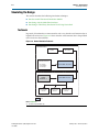
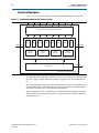
Block Description
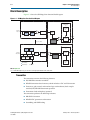
Figure 3–1 shows the SDI MegaCore function block diagram.
Figure 3–1. SDI MegaCore Function Block Diagram
Transmitter Transceiver
Transmitter Protocol Blocks
Transceiver
(1)
Transmitter
PLL
Parallel
Video In
FIFO
Buffer
Scrambler
Insert
CRC
Insert
LN
SDI Out
Parallelto-Serial
en_sync_switch
Transmitter
Oversampler
Receiver Transceiver
Receiver Protocol Blocks
Extract
LN
Transceiver
(1)
Check
CRC
Parallel
Video Out
SDI In
Aligner
Track
Ancilliary
Detect
Format
Serial-toParallel
Descrambler
TRS
Match
Receiver
Oversampler
Receiver
PLL
HD-SDI Only
SD-SDI Only
F, V, and H
Note to Figure 3–1:
(1) For SD-SDI designs only, you can have a soft-logic implementation of the transceiver.
Transmitter
The transmitter contains the following elements:
■
SD/HD-SDI transmitter scrambler
■
HD-SDI transmitter data formatter, which includes a CRC and LN insertion
■
Transceiver, plus control, and interface logic with multirate (dual or triple
standard) SD/HD-SDI transmitter operation
■
Transmitter clock multiplexer (optional)
The transmitter performs the following functions:
■
HD-SDI LN insertion
■
HD-SDI CRC generation and insertion
■
Scrambling and NRZI coding
Serial Digital Interface (SDI) MegaCore Function
User Guide
February 2013 Altera Corporation
Chapter 3: Functional Description
Block Description
■
3–3
Internal switching between two reference clock signals in the transmitter block.
This feature is optional and only available for Arria II GZ, Stratix IV GX , and
HardCopy IV devices.
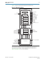
Figure 3–2 shows the top-level block diagram for the SDI transmitter.
Figure 3–2. SDI Transmitter Block Diagram
SDI TRANSMITTER
Protocol Block
rst_tx
tx_pclk
txdata[19:0]
tx_std[1:0]
tx_trs
tx_ln[21:0]
enable_ln
enable_crc
TRS Match
LN Insert
CRC (c)
CRC (y)
Scrambler
tx_data[19:0]
Transceiver Interface Block
rst_tx
tx_pclk
FIFO
tx_status
gxb_tx_clkout
GXB RX Sample
tx_clockout
tx_datain[19:0]
reset
tx_serial_refclk
tx_serial_refclk1 (optional)
gxb4_cal_clk
sdi_reconfig_togxb[3:0]
sdi_gxb_powerdown
sdi_tx (serial data)
sdi_reconfig_fromgxb[16
Transceiver Block
For HD-SDI, the transmitter accepts 20-bit parallel video data; for SD-SDI, 10-bit
parallel data. For txdata bus definition, refer to Table 3–16 on page 3–41.
February 2013
Altera Corporation
Serial Digital Interface (SDI) MegaCore Function
User Guide
3–4
Chapter 3: Functional Description
Block Description
Table 3–1 lists the bit allocation for txdata.
Table 3–1. Bit Allocation for txdata for Supported Video Standards
txdata
SD-SDI
HD-SDI
3G-SDI Level A
[19:10]
Unused
Y
Y
[9:0]
Cb, Y, Cr, Y
multiplex
C
C
3G-SDI Level B
Cb, Y, Cr, Y
multiplex (link A)
Cb, Y, Cr, Y
multiplex (link B)
For HD-SDI operation, the current video line number is inserted at the appropriate
point in each line. A CRC is also calculated and inserted for the luma and chroma
channels.
The parallel video data is scrambled and NRZI encoded according to the SDI
specification.
The transceiver converts the encoded parallel data into the high-speed serial output
(parallel-to-serial conversion).
HD-SDI LN Insertion
SMPTE292M section 5.4 defines the format of two words that are included in each
HD-SDI video line to indicate the current line number. The HD-SDI LN insertion
module takes the lower 11-bit tx_ln, and formats and inserts it as two words in the
output data. The HD-SDI LN insertion module accepts the current line number as an
input.
1
For more information about the line insertion for other video standards, refer to the
description for tx_ln signal in Table 3–16 on page 3–41.
The LN words (LN0 and LN1) overwrite the two words that follow the “XYZ” word
of the EAV TRS sequence. The same value is included in the luma and chroma
channels.
For correct LN insertion, you must assert the tx_trs signal must be asserted for the
first word of both EAV and SAV TRSs (refer to Figure 3–31 on page 3–47 and
Figure 3–32 on page 3–48).
1
If the system does not know the line number, you can implement logic to detect the
output video format and then determine the current line. This function is outside the
scope of this SDI MegaCore function.
HD-SDI CRC Generation and Insertion
SMPTE292M section 5.5 defines a CRC that is included in the chroma and luma
channels for each HD-SDI video line. The HD-SDI CRC module generates, formats,
and inserts the required CRC in the output data.
The HD-SDI CRC module identifies the words that you must include in the CRC
calculation, and also determines where you must insert the words in the output data.
The formatted CRC data words (YCR0 and YCR1 for the luma channel, CCR0 and CCR1
for the chroma channel) overwrite the two words that follow the line number words
after the EAV. A separate calculation is provided for the luma and chroma channels.
Serial Digital Interface (SDI) MegaCore Function
User Guide
February 2013 Altera Corporation
Chapter 3: Functional Description
Block Description
3–5
The CRC is calculated for all words in the active digital line, starting with the first
active word line and finishing with the final word of the line number (LN1). The initial
value of the CRC is set to zero, then the polynomial generator equation
CRC(X) = X18 + X5 + X4 + 1 is applied.
The HD-SDI CRC module implements the CRC calculation by iteratively applying the
polynomial generator equation to each bit of the output data, processing the LSB first.
For correct CRC generation and insertion, the tx_trs signal must be asserted for the
first word of both EAV and SAV TRS (refer to Figure 3–31 on page 3–47 and
Figure 3–32 on page 3–48).
Scrambling and NRZI Coding
SMPTE292M section 5 and SMPTE292M section 7 define a common channel coding
that is used for both SDI and HD-SDI. This channel coding consists of a scrambling
function (G1(X) = X9 + X4 + 1) followed by NRZI encoding (G2(X) = X + 1). The
scrambling module implements this channel coding. You can configure the module to
process either 10-bit or 20-bit parallel data.
The scrambling module implements the channel coding by iteratively applying the
scrambling and NRZI encoding algorithm to each bit of the output data, processing
the LSB first. Figure C.1 of SMPTE259M shows how the algorithm is implemented.
Transceiver Clock
Figure 3–3 shows the clocking scheme for the transmitter.
The tx_serial_refclk1 is an optional port that is enabled when you turn on the
Enable TX PLL select for 1/1.000 and 1/1.001 data rate reconfiguration in the SDI
parameter editor.
Figure 3–3. Transmitter Clocking Scheme
Protocol Block (Transmitter)
Transceiver Interface Block
gxb_tx_core_clk
Transceiver Block
ALTGXB
tx_clkout
gxb_tx_clkout
txdata[19:0]
encoded_data[19:0]
tx_pclk
gxb_txword[19:0]
tx_pclk
pll_inclk
pll_inclk1 (optional)
cal_blk_clk
reconfig_clk
sdi_tx
(serial data out)
tx_pclk
tx_serial_refclk
tx_serial_refclk1
gxb2_cal_clk
sdi_reconfig_clk
February 2013
Altera Corporation
Serial Digital Interface (SDI) MegaCore Function
User Guide
3–6
Chapter 3: Functional Description
Block Description
Receiver
The receiver contains the following elements:
■
Transceiver, plus control, and interface logic with multirate (dual or triple
standard) SD/HD-SDI receiver operation
■
SD/HD-SDI receiver descrambler and word aligner
■
HD-SDI receiver CRC and LN extractor
■
Receiver framing, with extraction of video timing signals
■
Identification and tracking of ancillary data
The SDI receiver consists of the following functions:
■
NRZI decoding and descrambling
■
Word alignment
■
Video timing flags extraction
■
RP168 switching compliance
■
HD-SDI LN extraction
■
HD-SDI CRC
■
Accessing transceiver
Serial Digital Interface (SDI) MegaCore Function
User Guide
February 2013 Altera Corporation
Chapter 3: Functional Description
Block Description
3–7
Figure 3–4 shows the top-level block diagram for the SDI receiver.
Figure 3–4. SDI Receiver Block Diagram
SDI RECEIVER
Protocol Block
Descrambler
rx_status[10:0]
rx_trs
rx_ln[21:0]
rxdata[19:0]
rx_data_valid_out[1:0]
crc_error_c[1:0]
crc_error_y[1:0]
rx_anc_data[19:0]
rx_anc_valid[3:0]
rx_anc_error[3:0]
rx_F[1:0]
rx_H[1:0]
rx_V[1:0]
rx_AP[1:0]
xyz_valid, rx_xyz, rx_eav
rst_rx
en_sync_switch
Aligner
LN Extract
CRC Extract
ANC Track
TRS Match
Format
rx_clk
rx_hd_sdi
word_valid
word[19:0]
Transceiver Interface Block
rst_rx
rx_serial_refclk
enable_sd_search
enable_hd_search
enable_3g_search
sdi_reconfig_done
GXB RX Sample
GXB Control FSM
Triple Rate Detect
digital_reset
analog_reset
lock_todata
lock_torefclk
rx_clockout
rx_dataout[19:0]
rst_rx
rx_serial_refclk
sdi_rx (serial data)
gxb4_cal_clk
sdi_reconfig_clk
sdi_reconfig_togxb[3:0]
sdi_gxb_powerdown
rx_clk
rx_std[1:0]
rx_std_flag_hd_sdn
sdi_start_reconfig
sdi_reconfig_fromgxb[16:0]
Transceiver Block
The received data is NRZI decoded and descrambled and then presented as a
word-aligned parallel output—20 bit for HD-SDI; 10 bit for SD-SDI (refer to
Table 3–16 on page 3–41 for rxdata bus definition).
February 2013
Altera Corporation
Serial Digital Interface (SDI) MegaCore Function
User Guide
3–8
Chapter 3: Functional Description
Block Description
Table 3–2 lists the bit allocation for rxdata.
Table 3–2. Bit Allocation for rxdata for Supported Video Standards
rxdata
[19:10]
[9:0]
SD-SDI
HD-SDI
3G-SDI Level A
Y
Y
C
C
Unused
Cb, Y, Cr, Y
multiplex
3G-SDI Level B
Cb, Y, Cr, Y
multiplex (link A)
Cb, Y, Cr, Y
multiplex (link B)
The receiver interface extracts and tracks the F, V, and H timing signals in the received
data. Active picture and ancillary data words are also identified for your use.
For HD-SDI, the received CRC is checked for the luma and chroma channels. The LN
is also extracted and provided as an output from the design.
NRZI Decoding and Descrambling
The descrambler module provides the channel decoding function that is common to
both SDI and HD-SDI. It implements the NRZI decoding followed by the required
descrambling. The algorithm indicated by SMPTE259M figure C.1 is iteratively
applied to the receiver data, with the LSB processed first.
Word Alignment
The aligner word aligns the descrambled receiver data such that the bit order of the
output data is the same as that of the original video data.
The EAV and SAV sequences determine the correct word alignment. Table 3–3 lists the
pattern for each standard.
Table 3–3. EAV and SAV Sequences
Video Standard
EAV and SAV Sequences
SDI
3FF 000 000
HD-SDI
3FF 3FF 000 000 000 000
3G-SDI Level A
3FF 3FF 000 000 000 000
3G-SDI Level B
3FF 3FF 3FF 3FF 000 000 000 000 000 000 000 000
The aligner matches the selected pattern in the descrambled receiver data. If the
pattern is detected at any of the possible word alignments, then a flag is raised and the
matched alignment is indicated. This process is applied continuously to the receiver
data.
The second stage of the aligner determines the correct word alignment for the data. It
looks for three consecutive TRSs with the same alignment, and then stores that
alignment. If two consecutive TRSs are subsequently detected with a different
alignment, then this new alignment is stored.
The final stage of the aligner applies a barrel shift function to the received data to
generate the correctly aligned parallel word output. For this SDI MegaCore function,
the barrel shifter allows the design to instantly switch from one alignment to another.
Serial Digital Interface (SDI) MegaCore Function
User Guide
February 2013 Altera Corporation
Chapter 3: Functional Description
Block Description
3–9
Video Timing Flags Extraction
The TRS match module extracts the F, V, and H video timing flags from the received
data. You can use these flags for receiver format detection, or in the implementation of
a flywheel function.
The TRS match module also identifies the line number and CRC words for HD-SDI.
RP168 Switching Compliance
To meet the RP168 requirements, the transceiver must be able to recover by the end of
the switching line. Table 3–4 lists the supported video switching type.
f For more information about the switching line and time for different video formats,
refer to RP168.
Table 3–4. Supported Video Switching Type
Standard/ Data Rate
Format
RP168 Support
Switching Source
Fixed
Switch (same format)
Yes
HD-1080i30 to HD-1080i30
Fixed
Switch
No
HD-1080 to HD-720
Switch
Fixed
No
HD-1080 to SD-525
Switch
Switch
No
HD-1080 to SD-525
Figure 3–5 and Figure 3–6 show the behaviors of the aligner and format blocks during
the RP168 switching.
The aligner block immediately aligns to the next TRS timing based on the user input
en_sync_switch signal.
Figure 3–5. Aligner Block Behavior
rx_data
10200
tx_data 10200
00000H
00000H
(1)
40020H
10200H
(2)
(3)
10200H
10200H
10200H
10200H
10200H
10200H
10200H
10200H
dead_time
switch
line
10
11
12
(2)
alignment
03H
12H
(4)
align_locked/rx_status[2]
Notes to Figure 3–5:
(1) Mismatch in alignment.
(2) New alignment on the next TRS.
(3) Data aligned to new alignment.
(4) Zero interrupt.
February 2013
Altera Corporation
Serial Digital Interface (SDI) MegaCore Function
User Guide
3–10
Chapter 3: Functional Description
Block Description
The format block latches the user input en_sync_switch signal for three lines to
realign to a new TRS alignment immediately. During switching, you see zero
interrupt at downstream. The trs_locked and frame_locked signals never get
deasserted during sync switch.
Figure 3–6. Format Block Behavior
en_sync_switch
en_sync_switch_reg
line
10
11
12
13
eav_detect
eav_position
2200
2199
(previous TRS timing)
2200
(new TRS timing)
trs_locked/rx_status[3]
frame_locked/rx_status[4]
HD-SDI LN Extraction
The HD-SDI LN extraction module extracts and formats the LN words defined by
SMPTE292M section 5.4 from the HD-SDI chroma channel. The design provides the
LN as an output.
HD-SDI CRC Checking
The CRC module checks the CRC defined by SMPTE292M section 5.5 for the HD-SDI
luma and chroma channels.
1
This module is common to the receiver and the transmitter.
The check is implemented by recalculating the CRCs for each received video line and
then checking the results against the CRC data received. If the results differ, an error
flag is asserted. There are separate error flags for the luma and chroma channels. The
flag is held asserted until the next check is performed.
Accessing Transceiver
The Quartus II software enables you to access the transceiver through the
unencrypted ALTGX wrapper file. You can access the ALTGX wrapper files for
Arria II GX, Arria V, Cyclone IV GX, Stratix II GX, and Stratix IV GX configurations.
You can use one of the two following ways to access the ALTGX wrapper files:
■
Edit the ALTGX wrapper file, using legal range provided in the respective device
handbooks.
■
Use analog control through the ALTGX_RECONFIG megafunction.
c Do not reinstantiate the customized ALTGX wrapper file using the MegaWizard
Plug-In Manager so that you do not lose the default content of the wrapper file after
regeneration.
Serial Digital Interface (SDI) MegaCore Function
User Guide
February 2013 Altera Corporation
Chapter 3: Functional Description
Block Description
3–11
Editing the ALTGX Wrapper File
If you want to change the settings of the parameters, edit the legal ranges in the
ALTGX wrapper file.
For example, if you want to change the voltage output differential control setting from
4 to 7, change the following line in the wrapper file:
alt4gxb_component.vod_ctrl_setting = 4
to this line:
alt4gxb_component.vod_ctrl_setting = 7
f To know the exact legal ranges for a specific Altera device, refer to the respective
device handbooks.
Using Analog Control
If you want the flexibility to access and control the ALTGX settings, use the
ALTGX_RECONFIG megafunction to enable analog reconfiguration. You can use the
analog control to edit the default settings of the following transceiver parameters:
■
Voltage output differential
■
Pre-emphasis control pre-tap
■
Pre-emphasis control 1st post-tap
■
Pre-emphasis control 2nd post-tap
■
Equalizer DC gain
■
Equalized DC control
The ALTGX_RECONFIG megafunction interfaces with the ALTGX using
reconfig_togxb[3:0] and reconfig_fromgxb[16:0] ports for a single channel.
To enable the analog control and channel reconfiguration during run time, use the
reconfig_mode_sel signal.
f For more information about how to use the analog control with the
ALTGX_RECONFIG megafunction, refer to the ALTGX_RECONFIG Megafunction
User Guide in the respective device handbooks.
February 2013
Altera Corporation
Serial Digital Interface (SDI) MegaCore Function
User Guide
3–12
Chapter 3: Functional Description
Block Description
Transceiver Clock
Figure 3–7 shows the general clocking scheme for the receiver.
Figure 3–7. Receiver Clocking Scheme
Protocol Block (Receiver)
Transceiver Interface Block
Transceiver Block
rxclk
rxclk
gxb_refclk
rxclk
ALTGXB
rx_clkout
rxdata[19:0]
rxword[19:0]
gxb_rxword[19:0]
rx_refclk
rx_dataout[19:0]
rx_cruclk
cal_blk_clk
reconfig_clk
sdi_rx
(serial data in)
rx_serial_refclk
gxb2_cal_clk
sdi_reconfig_clk
Transceiver—Soft-Logic Implementation
The soft-logic implementation differs for the transmitter and the receiver.
Transmitter
For the transmitter, in the soft-logic transceiver a 10-bit parallel word is converted into
a serial data output format. A 10-bit shift register loaded at the word rate from the
encoder and unloaded at the bit rate of the LVDS output buffer is implemented for
that function. A PLL that multiplies a 27-MHz reference clock by ten provides the
bit-rate clock and enables jitter-controlled SDI transmit serialization.
Transmitter Clocks
The serializer requires a 270-MHz clock, which you can generate from an external
source (tx_sd_refclk_270).
The 27-MHz parallel video clock (tx_pclk) samples and processes the parallel video
input.
Transmitter Clock Multiplexer Option
This is a new feature introduced in version 11.1. The transmitter block has the option
of receiving an additional reference clock to allow dynamic switching between the
1/1000 and 1/1.001 data rates. This feature is available in Arria II, Stratix IV, and
HardCopy IV devices.
By default, you can use the tx_serial_refclk for any normal SDI operations and the
tx_serial_refclk1 as an additional clock input parameter. You can then switch to the
clock source selected by using the transceiver dynamic reconfiguration.
Serial Digital Interface (SDI) MegaCore Function
User Guide
February 2013 Altera Corporation
Chapter 3: Functional Description
Block Description
3–13
Receiver
For the receiver, in the soft-logic transceiver the serial data stream from the LVDS
input buffer is sampled using four different clocks phase-shifted by 90° from each
other. Two out of these four clocks are created from an on-chip PLL. The two
remaining clocks are created by inversion of the PLL clock outputs.
Samples are then all converted to the same clock domain and deserialized into a 10-bit
parallel word. The serial clock that samples the bit stream must be 337.5 MHz, which
is 5/4 of the incoming bit (270-bit rate × 5/4 × 4 sample per clock = 1,350 Mbps)
The parallel clock that extracts data from the deserializer is running at 135 MHz.
To achieve timing, you must correctly constrain your design, refer to “Constraints” on
page A–1.
Receiver Clocks
The deserializer requires three clocks (refer to Table 3–15 on page 3–41), which you
can generate from an external source.
Transceiver—Stratix GX Devices
The Stratix GX transceiver deserializes the high-speed serial input. For HD-SDI, the
clock data recovery (CDR) function performs the deserialization and locks the
receiver PLL to the receiver data. For SD-SDI, the transceiver provides a fixed
frequency oversample of the serial data with the receiver PLL constantly locked to a
reference clock, which allows the transceiver to support the 270-Mbps data rate.
The transceiver can process either SD-SDI or HD-SDI data. The data rate can be
automatically detected so that the interface can handle both SD-SDI and HD-SDI
without the need for device reconfiguration.
In Stratix GX devices, the transmitters in a quad share a common reference clock,
which prevents them from operating independently.
Receivers in a quad share a common training clock, but have independent receiver
PLLs. Because the same training clock is used for SD-SDI and HD-SDI, receivers can
accommodate the different standards within a single quad.
Transmitter Clocks
The transmitter requires two clocks: a parallel video clock (tx_pclk) and a transmitter
reference clock (tx_serial_refclk).
The parallel video clock samples and processes the parallel video input. For SD-SDI, it
is 27 MHz; for HD-SDI, it is 74.25 or 74.175 MHz.
The transceiver uses the transmitter reference clock to generate the high-speed serial
output. The transceiver is configured for 20-bit operation, so the reference clock is
1/20th of the serial data rate.
1
For SD-SDI, because of the oversampling implementation, the serial data rate is five
times the SDI bit rate (for example, 1,350 Mbps).
For HD-SDI operation, pclk can drive the transmitter reference clock.
February 2013
Altera Corporation
Serial Digital Interface (SDI) MegaCore Function
User Guide
3–14
Chapter 3: Functional Description
Block Description
For SD-SDI operation, you can derive the transmitter reference clock from pclk by
using one of the Stratix GX PLLs. The PLL can multiply the 27-MHz pclk signal by
5/2.
For dual standard operation, use an external multiplexer to select between the SD-SDI
and HD-SDI reference clock.
The Stratix GX architecture allows each group of four transmitters (a transceiver
quad) to have a separate transmitter reference clock.
Table 3–5 lists frequencies of the transmitter clock, tx_serial_refclk, for Stratix GX
devices.
Table 3–5. Transmitter Clock Frequency—Stratix GX Devices
Video Standard (1)
Clock Frequency (MHz)
SD-SDI
67.5
HD-SDI (including dual link)
74.175/74.25
(2)
HD-SDI with two times oversample
148.35/148.5
(2)
Dual standard
67.5/74.175/74.25
(2)
Notes to Table 3–5:
(1) Stratix GX devices do not support 3G and triple standard modes.
(2) The tx_serial_refclk signal must be externally multiplexed.
Figure 3–8 shows the transmitter clocks for different video standards.
Figure 3–8. Transmitter Clocks—Stratix GX Devices
SD-SDI
SDI MegaCore
Function
Serial Data
67.5 MHz
from PLL or Pin
HD-SDI
SDI MegaCore
Function
Serial Data
74.XX MHz (1)
from reference clock
Dual Standard
SDI MegaCore
Function
Serial Data
67.5 MHz
74.XX MHz (1)
(2)
Notes to Figure 3–8:
(1) This frequency can be either 74.175 or 74.25 MHz, to support 1.4835 or 1.485 Gbps HD-SDI respectively.
(2) The multiplexer must not be in the device.
Serial Digital Interface (SDI) MegaCore Function
User Guide
February 2013 Altera Corporation
Chapter 3: Functional Description
Block Description
3–15
Receiver Clocks
The transceiver requires a receiver reference clock, rx_serial_refclk. This clock
trains the receiver PLL in the transceiver.
For HD-SDI operation, the clock must be nominally 1/20th of the serial data rate. The
clock do not have to operate at the data rate, because it is only used for the training of
the receiver PLL.
For SD-SDI operation, the clock must be nominally 1/4th of the serial data rate (for
example, 67.5 MHz). The clock do not have to be frequency-locked to the data.
For dual standard operation, the receiver reference clock must be 67.5 MHz, which
allows the transceiver to sample the data for SD-SDI at the correct frequency. For
HD-SDI, the receiver PLL trains with the 67.5-MHz reference, and then tracks to the
actual incoming data rate.
All receiver interfaces can share a common receiver reference clock.
Table 3–6 lists the frequencies of the receiver clock, rx_serial_refclk, for Stratix GX
devices.
Table 3–6. Receiver Clock Frequency—Stratix GX Devices
Video Standard (1)
Clock Frequency (MHz)
SD-SDI
67.5
HD-SDI (including dual link)
74.175/74.25
Dual standard
(2)
67.5
Notes to Table 3–6:
(1) Stratix GX devices do not support 3G-SDI and triple standard modes.
(2) The rx_serial_refclk signal must be externally multiplexed.
February 2013
Altera Corporation
Serial Digital Interface (SDI) MegaCore Function
User Guide
3–16
Chapter 3: Functional Description
Block Description
Figure 3–9 shows the receiver clocks for different video standards.
Figure 3–9. Receiver Clocks
SD-SDI
SDI MegaCore
Function
Serial Data
rx_clk = 67.5 MHz
rx_data_valid_out
rx_clk
rx_data
V
V
V
V
rx_data_valid_out
67.5 MHz
HD-SDI
SDI MegaCore
Function
Serial Data
rx_clk = 74.25 MHz
rx_data_valid_out
rx_clk
rx_data
V
V
V
V
rx_data_valid_out
74.25/74.175 MHz
Dual Standard
SDI MegaCore
Function
Serial Data
rx_clk = 67.5 or 74 MHz
rx_data_valid_out
67.5 MHz
Transmitter Transceiver Interface
Altera provides a transceiver interface, which interfaces the transceiver to the SDI
function. The transceiver interface implements the following functions:
1
■
Transmitter Retiming
■
HD-SDI Two-Times Oversampling
■
SD-SDI Transmitter Oversampling
When using the two-times oversampling transmitters in Stratix GX devices, you
cannot have HD-SDI receivers in the same quad. The quad requires the same
frequency reference clocks for both the receivers and transmitters within a quad.
HD-SDI receivers and two-times oversampling transmitters have different frequency
reference clocks (refer to Table 3–5 and Table 3–6 on page 3–15).
Transmitter Retiming
The txdata parallel data input to the transceiver must be synchronous and phase
aligned to the tx_coreclk transceiver clock input. SD-SDI (and optionally HD-SDI)
requires a retiming function, because of the oversampling logic. The transmitter uses a
small 16 × 20 FIFO buffer for the retiming.
Serial Digital Interface (SDI) MegaCore Function
User Guide
February 2013 Altera Corporation
Chapter 3: Functional Description
Block Description
3–17
For HD-SDI, the FIFO buffer realigns the parallel video input to the transceiver
tx_coreclk clock. It is written on every tx_pclk clock, and read on every tx_coreclk.
For SD-SDI, the FIFO buffer also provides the rate conversion required by the
transmitter oversampling logic. It is written on every other tx_pclk, using the SD-SDI
data width conversion logic. It is read on every fifth tx_coreclk. This operation
ensures that the transmitter oversampling logic is provided with a word of parallel
video data on every fifth clock.
HD-SDI Two-Times Oversampling
This mode performs two-times oversampling and runs the transceiver at double rate,
which gives better output jitter performance. This mode requires a higher rate
reference clock, refer to Table 3–5 on page 3–14.
SD-SDI Transmitter Oversampling
SD-SDI requires a 270-Mbps serial data rate, which is achieved by transmitting a
1,350 Mbps signal with each bit repeated five times. This process ensures that the
transceiver runs at a supported frequency.
Receiver Transceiver Interface
Altera provides a transceiver interface, which interfaces the transceiver to the SDI
function. The transceiver interface implements the following functions:
1
■
SD-SDI Receiver Oversampling
■
Transceiver Controller
When using the two-times oversampling transmitters in Stratix GX devices, you
cannot have HD-SDI receivers in the same quad. The quad requires the same
frequency reference clocks for both the receivers and transmitters within a quad.
HD-SDI receivers and two-times oversampling transmitters have different frequency
reference clocks (refer to Table 3–5 on page 3–14 and Table 3–6 on page 3–15).
SD-SDI Receiver Oversampling
The Stratix GX transceiver does not support CDR for data rates less than 500 Mbps.
The receiver uses fixed frequency oversampling for the reception of 270-Mbps
SD-SDI. The serial data is sampled by the transceiver at 1,350 Mbps and the original
270-Mbps data is extracted by the SD-SDI receiver oversampling logic.
Figure 3–10 shows an example of the receiver data timing.
Figure 3–10. Receiver Data Timing
rx_clk (67.5MHz)
rxdata
DATA
rx_data_valid_out
February 2013
Altera Corporation
Serial Digital Interface (SDI) MegaCore Function
User Guide
3–18
Chapter 3: Functional Description
Block Description
Transceiver Controller
To achieve the desired receiver functionality for the SDI, the transceiver controller
controls the transceiver.
When the interface receives SD-SDI, the transceiver receiver PLL locks to the receiver
reference clock.
When the interface receives HD-SDI, the transceiver receiver PLL is first trained by
locking to the receiver reference clock. When the PLL is locked, it can then track the
actual receiver data rate. If a period of time passes without a valid SDI signal, the PLL
is retrained with the reference clock and the process is repeated.
The transceiver controller allows the transceiver to support the reception of both
SD-SDI and HD-SDI data by using an algorithm that alternately searches for one rate
then the other. First, it looks for an HD-SDI signal, training the PLL then letting it
track the serial data rate. If a valid HD-SDI signal is not seen within 0.1 s, the receiver
path is reset and the PLL is trained for SD-SDI. Conversely, if a valid SD-SDI signal is
not seen within 0.1 s, the receiver path is reset and the process repeated. The
transceiver controller also resets and starts searching again if the SDI receiver
indicates that the signal is no longer valid.
For HD-SDI operation, if 100 consecutive bits with the same value are seen, the
receiver is reset and the PLL is retrained. The maximum legal run length for HD-SDI
is 59 bits.
f For more information on the Stratix GX transceiver, refer to the Stratix GX Device
Handbook.
Transceiver—Arria GX, Arria II GX, Arria V, Cyclone IV GX, Cyclone V,
Stratix II GX, Stratix IV GX, and Stratix V Devices
The Arria GX, Arria II GX, Arria V, Cyclone IV GX, Stratix II GX, Stratix IV GX, or
Stratix V transceiver deserializes the high-speed serial input. For HD-SDI, the CDR
function performs the deserialization and locks the receiver PLL to the receiver data.
For SD-SDI, the transceiver provides a fixed frequency oversample of the serial data
with the receiver PLL constantly locked to a reference clock, which allows the
transceiver to support the 270-Mbps data rate.
The transceiver can process either SD-SDI or HD-SDI data. The data rate can be
automatically detected so that the interface can handle both SD-SDI and HD-SDI
without the need for device reconfiguration.
Arria GX, Arria II GX, Arria V, Stratix II GX, Stratix IV GX, and Stratix V devices have
two transmitter PLLs per quad. Each quad allows two independent transmitter rates.
Receivers in a quad share a common training clock, but have independent receiver
PLLs. Because the same training clock is used for SD-SDI and HD-SDI, receivers can
accommodate the different standards within a single quad.
Arria II GX (including Arria II GZ) and Stratix IV GX devices also provide the option
for you to enable an additional serial reference clock port. This additional clock port
allows you to have two different clock rates for different data rates using a single
transceiver block, with the ability to switch between the desired clock rates (for
example, 148.5 MHz and 148.35 MHz).
Serial Digital Interface (SDI) MegaCore Function
User Guide
February 2013 Altera Corporation
Chapter 3: Functional Description
Block Description
3–19
Cyclone IV GX devices—EP4CGX30 (F484), EP4CGX50, EP4CGX75, EP4CGX110, and
EP4CGX150—have eight regular transceiver channels from the upper and lower
quads. There are four MPLLs and two GPLLs that you can use to clock the transceiver
channels. Each receiver in EP4CGX50 and EP4CGX75 devices has a clock divider,
which allows one MPLL to drive all the receiver channels. The receiver in EP4CGX110
and EP4CGX150 devices does not have a clock divider, which limits each MPLL to
drive only one receiver channel to accommodate the different standards within a
single quad.
You must supply two receive reference clocks (for example, 148.5 MHz and
148.35 MHz) to the SDI receiver. Implement the PPM detection function in the user
logic to detect the ppm difference between the receive reference clock and the
recovered clock. Based on the difference detected, you must switch between the two
receive reference clocks by toggling the rx_serial_refclk_clkswitch signal,
(Table 3–16 on page 3–41).
f For more information about the Cyclone IV GX transceiver architecture, refer to
Cyclone IV Transceivers Architecture chapter in volume 2 of the Cyclone IV Device
Handbook.
Cyclone V devices have up to 12 transceiver channels. The SDI support for Cyclone V
transceivers requires the use of the Cyclone V Transceiver Native PHY IP Core. The
native PHY is a thin IP layer with an embedded transceiver PLL.
The Cyclone V Transceiver Native PHY IP Core provides direct access to all control
and status signals of the transceiver channels. Unlike other PHY IP cores, the Native
PHY IP Core does not include an Avalon Memory-Mapped (Avalon-MM) interface.
Instead, it exposes all signals directly as ports. The Cyclone V Transceiver Native PHY
IP Core includes the Standard PCS. You can select the PCS functions and control and
status port that your transceiver PHY requires. The Native Transceiver PHY does not
include an embedded reset controller.
f For more information about the Cyclone V Transceiver Native PHY IP Core, refer to
the Altera Transceiver PHY IP Core User Guide.
Transmitter Clocks
The transmitter requires two clocks: a parallel video clock (tx_pclk) and a transmitter
reference clock (tx_serial_refclk).
The parallel video clock samples and processes the parallel video input. For SD-SDI, it
is 27 MHz; for HD-SDI, it is 74.25 or 74.175 MHz; for 3G-SDI, it is 148.5 or 148.35 MHz.
The transceiver uses the transmitter reference clock to generate the high-speed serial
output. The transceiver is configured for 20-bit operation, so the reference clock is
1/20th of the serial data rate.
1
For SD-SDI, because of the oversampling implementation, the serial data rate is five
times the SDI bit rate (for example, 1,350 Mbps); for the triple-standard SDI,
the oversampling rate is 11.
For SD-SDI operation, the transmitter reference clock can be derived from pclk by
using one of the transceiver PLLs. The PLL can multiply the 27-MHz pclk signal by
5/2.
February 2013
Altera Corporation
Serial Digital Interface (SDI) MegaCore Function
User Guide
3–20
Chapter 3: Functional Description
Block Description
For all other standards, use an external multiplexer to select between the alternative
reference clocks.
Table 3–7 lists the frequencies of the transmitter clock, tx_serial_refclk, for
Arria GX, Arria II GX, Arria V, Cyclone IV GX, Cyclone V, Stratix II GX, Stratix IV, and
Stratix V devices.
Table 3–7. Transmitter Clock Frequency—Arria GX, Arria II GX, Arria V, Cyclone IV GX,
Cyclone V, Stratix II GX, Stratix IV, and Stratix V Devices
Video Standard
SD-SDI
Clock Frequency (MHz)
67.5
HD-SDI (including dual link)
74.175/74.25
(1)
HD-SDI with two times oversample
148.35/148.5
(1)
Dual standard
67.5/74.175/74.25
Triple standard
148.35/148.5
(1)
3G-SDI
148.35/148.5
(1)
(1)
Note to Table 3–7:
(1) The tx_serial_refclk signal must be externally multiplexed. If additional input reference clock port is enabled
for serial reference clock, external multiplier is no longer required.
Serial Digital Interface (SDI) MegaCore Function
User Guide
February 2013 Altera Corporation
Chapter 3: Functional Description
Block Description
3–21
Figure 3–11 shows the transmitter clocks for different video standards.
Figure 3–11. Transmitter Clocks—Arria GX, Arria II GX, Arria V, Cyclone IV GX, Cyclone V,
Stratix II GX, Stratix IV, and Stratix V Devices
SD-SDI
SDI MegaCore
Function
Serial Data
67.5 MHz
from PLL or Pin
HD-SDI
SDI MegaCore
Function
Serial Data
74.XX MHz (1)
from reference clock
Dual Standard
SDI MegaCore
Function
Serial Data
67.5 MHz
74.XX MHz (1)
(2)
3G-SDI or Triple Standard
SDI MegaCore
Function
Serial Data
148.XX MHz (3)
from reference clock
3G-SDI or Triple Standard (with additional reference clock port)
SDI MegaCore
Function
148.35 MHz (4)
Serial Data
148.5 MHz
Notes to Figure 3–11:
(1) This frequency can be either 74.175 or 74.25 MHz, to support 1.4835 or 1.485 Gbps HD-SDI respectively.
(2) The multiplexer must not be in the device.
(3) This frequency can be either 148.35 or 148.5 MHz, to support 2.967 or 2.970 Gbps HD-SDI respectively.
(4) You can source both 148.5 MHz and 148.35 MHz together if the additional clock port is enabled.
February 2013
Altera Corporation
Serial Digital Interface (SDI) MegaCore Function
User Guide
3–22
Chapter 3: Functional Description
Block Description
Receiver Clocks
The transceiver requires a receiver reference clock, rx_serial_refclk. This clock
trains the receiver PLL in the transceiver.
For HD-SDI operation, the clock must be nominally 1/20th of the serial data rate. The
clock does not have to be frequency locked to the data, because the design only uses it
for the training of the receiver PLL.
For SD-SDI operation, the clock must be nominally 1/4th of the serial data rate
(for example, 67.5 MHz). The clock does not have to be frequency locked to the data.
For dual or triple standard operation, the receiver reference clock must be 148.5 MHz.
In this mode, the transceiver oversamples the SD-SDI signals by a factor of 11.
All receiver interfaces can share a common receiver reference clock.
Table 3–8 shows the receiver clock rx_serial_refclk frequencies.
Table 3–8. Receiver Clock Frequency—Arria GX, Arria II GX, Arria V, Cyclone IV GX, Cyclone V,
Stratix II GX, Stratix IV, and Stratix V Devices
Video Standard
SD-SDI
HD-SDI (including dual link)
Dual or triple standard
3G-SDI
Clock Frequency (MHz)
67.5
74.175/74.25
148.35/148.5
(1)
(1), (2)
148.35/148.5
(1)
Notes to Table 3–8:
(1) You can use either reference clock for training.
(2) Must be 148.5 MHz for correct SD-SDI operation.
Serial Digital Interface (SDI) MegaCore Function
User Guide
February 2013 Altera Corporation
Chapter 3: Functional Description
Block Description
3–23
Figure 3–12 shows the receiver clocks for different video standards.
Figure 3–12. Receiver Clocks
SD-SDI
SDI MegaCore
Function
Serial Data
rx_clk
rx_clk = 67.5 or 74 MHz
rx_data_valid_out
rx_data
V
V
V
V
rx_data_valid_out
67.5 MHz
HD-SDI
SDI MegaCore
Function
Serial Data
rx_clk = 74.175 or 74.25 MHz
rx_data_valid_out
rx_clk
rx_data
V
V
V
V
rx_data_valid_out
74.25 or 74.175 MHz
3G-SDI or Dual Standard or Triple Standard
SDI MegaCore
Function
Serial Data
rx_clk = 148.5 MHz (or 74.xx MHz when receiving HD)
rx_data_valid_out
148.5 MHz
Transmitter Transceiver Interface
Altera provides a transceiver interface, which interfaces the transceiver to the SDI
function. The transceiver interface implements the following functions:
■
Retiming from the parallel video clock domain to the transceiver transmitter clock
domain
■
Optional two-times oversampling for HD
■
Transmitter oversampling for SD
Transmitter Retiming
The txdata parallel data input to the transceiver must be synchronous and phase
aligned to the tx_coreclk transceiver clock input. SD-SDI (and optionally HD-SDI)
requires a retiming function, because of the oversampling logic. The transmitter uses a
small 16 × 20 FIFO buffer for the retiming.
For HD-SDI, the FIFO buffer realigns the parallel video input to the transceiver
tx_coreclk clock. It is written on every tx_pclk clock, and read on every tx_coreclk.
February 2013
Altera Corporation
Serial Digital Interface (SDI) MegaCore Function
User Guide
3–24
Chapter 3: Functional Description
Block Description
For SD-SDI, the FIFO buffer also provides the rate conversion required by the
transmitter oversampling logic. It is written on every other tx_pclk, using the SD-SDI
data width conversion logic. It is read on every fifth or eleventh tx_coreclk. This
operation ensures that the transmitter oversampling logic is provided with a word of
parallel video data on every fifth or eleventh clock.
HD-SDI Two-Times Oversampling
This mode performs two-times oversampling and runs the transceiver at double rate,
which gives better output jitter performance. This mode requires a higher rate
reference clock, refer to Table 3–5 on page 3–14.
SD-SDI Transmitter Oversampling
SD-SDI requires a 270-Mbps serial data rate, which is achieved by transmitting a
1,350 Mbps signal with each bit repeated five times. This process ensures that the
transceiver runs at a supported frequency. In triple standard mode, bit are transmitted
at 2,970 Mbps with each bit repeated 11 times.
Receiver Transceiver Interface
Altera provides a transceiver interface, which interfaces the transceiver to the SDI
function. The transceiver interface implements the following functions:
■
SD-SDI Receiver Oversampling
■
Transceiver Controller
SD-SDI Receiver Oversampling
Arria GX and Stratix II GX transceivers do not support CDR for data rates less than
622 Mbps. Arria II GX, Arria V, Stratix IV, and Stratix V transceivers do not support
CDR for data rates less than 600 Mbps. The receiver uses fixed frequency
oversampling for the reception of 270-Mbps SD-SDI. The transceiver samples the
serial data at 1,350 or 2,970 Mbps and the SD-SDI receiver oversampling logic extracts
the original 270 Mbps data.
Figure 3–13 shows an example of the receiver data timing.
Figure 3–13. Receiver Data Timing
rx_clk (67.5MHz)
rxdata
DATA
rx_data_valid_out
Transceiver Controller
To achieve the desired receiver functionality for the SDI, the transceiver controller
controls the transceiver.
When the interface receives SD-SDI, the transceiver receiver PLL locks to the receiver
reference clock.
When the interface receives HD-SDI, the transceiver receiver PLL is first trained by
locking to the receiver reference clock. When the PLL is locked, it can then track the
actual receiver data rate. If a period of time passes without a valid SDI signal, the PLL
is retrained with the reference clock and the process is repeated.
Serial Digital Interface (SDI) MegaCore Function
User Guide
February 2013 Altera Corporation
Chapter 3: Functional Description
Block Description
3–25
First, the transceiver controller makes a coarse rate detection of the incoming data
stream. Then, the transceiver is reprogrammed using transceiver dynamic
reconfiguration (refer to “Transceiver Dynamic Reconfiguration for Dual Standard
and Triple Standard Receivers” on page 3–27 and “Transceiver Dynamic
Reconfiguration with PLL Reconfiguration Mode—Cyclone IV GX” on page 3–33) to
the correct rate for the standard that has been detected. After the reprogramming, the
transceiver attempts to lock to the incoming stream. If no valid data is seen in 0.1 s, the
receiver path is reset and the rate detection is performed again.
At the start of the rate detection process, the level of the three enable_xx signals is
sampled. The level of these signals and the knowledge of the currently programmed
state of the transceiver determines if the transceiver requires programming. This
process ensures that the transceiver is reprogrammed only when necessary.
Locking to the Incoming SDI Stream
The transceiver control state machine uses the presence (or absence) of TRSs on the
stream to determine if SDI is being correctly received. A single, valid TRS indicates to
the control state machine that the receiver is acquiring some valid SDI samples. The
control state machine only deasserts this flag when it does not detect any EAV
sequences within the number of consecutive lines you specified. At this point, the
controller state machine resets and performs the relock algorithm, refer to
Figure 3–14.
Figure 3–14. Locking Algorithm
trs_strobe
n-th missing EAV New TRS reasserts
word count
trs_loose_lock
Because the aligner realigns to a new alignment if two consecutive TRSs with the
same alignment are detected, this scheme allows for an SDI source switch and an
alignment change without affecting the transceiver reset state machine.
The SDI MegaCore function also monitors the incoming EAV and SAV signals to
ensure their spacing is consistent over a number of lines. The MegaCore function
monitors by incrementing a counter on each incoming SDI word and storing the count
values at which an EAV or SAV is detected. If the EAV and SAV spacing is consistent
over 6 video lines, the MegaCore function indicates trs_locked on the rx_status[3]
output.
An enhancement in the current SDI MegaCore function allows a number of missing
EAV or SAV that you specify to be tolerated without deasserting the trs_locked
signal.
For example, when you specify the Tolerance to consecutive missed EAV/SAV
parameter to 2, one or two consecutive missing EAVs set a “missed” flag but do not
cause the trs_locked signal to deassert. A good EAV in the correct position resets the
“missed” flag.
The operation of this missing or misplaced TRS tolerance is shown in Figure 3–15,
Figure 3–16, and Figure 3–17.
February 2013
Altera Corporation
Serial Digital Interface (SDI) MegaCore Function
User Guide
3–26
Chapter 3: Functional Description
Block Description
Figure 3–15 and Figure 3–16 show how one or two consecutive missing EAVs do not
cause the trs_locked signal to deassert.
Figure 3–15. Single Missing EAV Signal
Error in EAV
SAV
data
EAV
SAV
EAV
SAV
trs_strobe
prev_eav_missed
g host_eav
trs_locked
Figure 3–16. Two Consecutive Missing EAV Signal
1st error in EAV
SAV
data
EAV
SAV
2nd error in EAV
SAV
trs_strobe
prev_eav_missed
g host_eav
trs_locked
Figure 3–17 shows how three consecutive missing EAVs cause the trs_locked signal
to deassert.
Figure 3–17. Three Consecutive Missing EAV Signal
1st error in EAV
SAV
3rd error in EAV
SAV
data
EAV
SAV
2nd error in EAV
SAV
trs_strobe
prev_eav_missed
g host_eav
trs_locked
The frame_locked signal detects TRS EAV, inspects the transition of field (F) and
vertical (V) synchronizations, and then counts the line number. The inspecting
transitions on the F and V synchronizations provide the frame timing. The line count
value is stored if there is a rising or falling edge on the F and V synchronizations
through the frame. The stored count values are compared over multiple frames to
make sure they are stable, before the frame_locked signal is asserted.
The frame_locked signal deasserts when there are bad F or V synchronizations, or
when there is a rising edge from frame to frame. The frame_locked signal also
deasserts when the trs_locked signal deasserts.
When the frame_locked signal is zero, the frame is invalid, and the receiver is not
considered to receive reliable video data.
Serial Digital Interface (SDI) MegaCore Function
User Guide
February 2013 Altera Corporation
Chapter 3: Functional Description
Block Description
3–27
Transceiver Dynamic Reconfiguration for Dual Standard and Triple
Standard Receivers
Dual standard and triple standard SDI receivers (or receivers of duplex SDIs) require
the transceiver dynamic reconfiguration feature of Arria GX, Arria II GX,
Cyclone IV GX, Stratix II GX, and Stratix IV devices to perform autodetection and
locking to different SDI rates.
Table 3–9 lists the transceiver dynamic reconfiguration support for Arria II GX,
Cyclone IV GX, HardCopy IV GX, Stratix GX, Stratix II GX, and Stratix IV GX devices.
Table 3–9. Transceiver Dynamic Reconfiguration Support for Altera Devices (1)
Arria II GX, HardCopy IV GX, Stratix GX,
Stratix II GX,
and Stratix IV GX
Cyclone IV GX
(EP4CGX50, EP4CGX75)
Cyclone IV GX
(EP4CGX110,
EP4CGX150) (2)
Channel Reconfiguration
Yes
Yes
No
PLL Reconfiguration
No
Yes
Yes
Transceiver Reconfiguration
No
No
No
Transceiver Dynamic
Reconfiguration Support
Note to Table 3–9:
(1) The SDI MegaCore function versions 10.1 and later do not support MIF generation for EP4CGX30 (F484), EP4CGX50, and EP4CGX75.
(2) The ALTGX_RECONFIG is required for offset cancellation purposes for all transceiver instances.
f For more information about transceiver dynamic reconfiguration, refer to the
Arria GX Device Handbook, Arria II GX Device Handbook, Cyclone IV Device Handbook,
Stratix II GX Device Handbook, and Stratix IV Device Handbook.
Transceiver Dynamic Reconfiguration with Channel Reconfiguration Mode—
Arria II GX, HardCopy IV GX, Stratix GX, Stratix II GX, and
Stratix IV GX
Transceiver dynamic reconfiguration allows you to change the settings of the device
transceivers (ALT2GXB or ALTGX) at any time. Transceiver dynamic reconfiguration
reprograms the transceivers to support the three SDI rates.
The triple standard SDI uses 11 times oversampling for receiving SD-SDI. Hence, only
Arria II GX or Stratix II GX transceiver configurations are required as the rates for
3G-SDI and SD-SDI 11 times are the same.
February 2013
Altera Corporation
Serial Digital Interface (SDI) MegaCore Function
User Guide
3–28
Chapter 3: Functional Description
Block Description
Table 3–10 lists the transceiver dynamic reconfiguration requirements.
Table 3–10. Transceiver Dynamic Reconfiguration Requirements
SDI Standard
Receiver
Transmitter
(1)
Duplex
SD-SDI
No
Yes
Yes
HD-SDI
No
Yes
Yes
3G-SDI
No
Yes
Yes
Dual link
No
Yes
Yes
Dual standard
Yes
Yes
Yes
Triple standard
Yes
Yes
Yes
(1)
Note to Table 3–10:
(1) If the additional serial reference clock feature is enabled, the transmitters require dynamic reconfiguration to
enable toggling switching between the two input clocks.
Table 3–11 lists the rates for the different SDI standards.
Table 3–11. SDI Standard Rates
SDI Standard
Data Rate
Oversampling
Transceiver
Rate (MHz)
Transceiver
Reference Clock
(MHz)
rx_clk Rate
SD-SDI
270 Mbps
11 times
2,970
148.5
148.5
HD-SDI
1.485 Gbps
None
1,485
148.5
(1)
3G-SDI
2.970 Gbps
None
2,970
148.5
(1)
74.25
(1)
148.5
(1)
Note to Table 3–11:
(1) Also supports the 1/1.001 rates for all supported devices, except Cyclone IV GX devices. For Cyclone IV GX
devices, the transceiver reference clock must be 148.35 MHz to support the 1/1.001 rates.
To reprogram the transceivers, you must include the ALT2GXB_RECONFIG or
ALTGX_RECONFIG megafunction in your design. However, to reprogram
Arria II GX or Stratix IV device family, you require an ALTGX_RECONFIG
megafunction. You can get this parameterization from the
example\a2gx_tr\source\sdi_dprio_siv directory in the example design. Similarly,
to reprogram Cyclone IV GX device family with channel reconfiguration mode, you
require a slightly different configuration of the ALTGX_RECONFIG megafunction.
You can get this parameterization from the
simulation\modelsim\trsdi_c4gx\channel_reconfig\testbench\pattern_gen
directory in the example simulation.
f For more information about the ALT2GXB_RECONFIG megafunction, refer to the
Stratix II GX ALT2GXB_RECONFIG Megafunction User Guide. For more information
about the ALTGX_RECONFIG megafunction, refer to the Stratix IV
ALTGX_RECONFIG Megafunction User Guide.
Serial Digital Interface (SDI) MegaCore Function
User Guide
February 2013 Altera Corporation
Chapter 3: Functional Description
Block Description
3–29
Transceiver Reconfiguration for Transmitter Clock Multiplexer
The transmitter reconfiguration requires its own Memory Initialization Files (.mif)
that is stored in the device. The .mif contains information about the default selection
of the TX PLL that is based on the logical_tx_pll_sel and logical_tx_pll_sel_en
pins. These pins are available in the transceiver port when you enable the transmitter
clock multiplexer feature. By toggling the values in these ports and reconfiguring the
transmitter megafunction, you can internally switch the TX PLL to select different
reference clock inputs. For Arria II and Stratix IV devices, these are 19-words by 16bits files. The following are the sequence of events that occur during the SDI
transmitter clock toggling:
1. SDI MegaCore function detects a change request to the serial reference clock.
2. The ALTGX_RECONFIG block reads the appropriate ROM, sets the
logical_tx_pll_sel and logical_tx_pll_sel_en ports to the required value, and
reprograms the ALTGX in the transmitter block.
3. When step 2 is completed, the SDI transmitter begins locking on the new serial
reference clock.
1
User logic is required in handling the handshaking between the SDI MegaCore
function and the ALTGX_RECONFIG block.
1
By default, the receiver reconfiguration has higher priority than the transmitter
reconfiguration.
Transceiver Reconfiguration for Receiver
The ROMs store the alternative setups for the transceiver settings within the device.
These setups are 28 words by 16 bits for Arria GX and Stratix II GX devices, and
38 words by 16 bits for Arria II and Stratix IV devices. The ALT2GXB megafunction
has a serial reprogramming interface, so the ALT2GXB_RECONFIG block must
serialize this parallel data before loading.
The following sequence of events occur during an SDI receiver rate change:
1. SDI MegaCore function detects the incoming video rate and requests
reprogramming.
2. The ALT2GXB_RECONFIG block reads the appropriate ROM, serializes the data,
and applies the serial data to the correct transceiver instance.
3. When step 2 is completed, the ALT2GXB_RECONFIG block indicates to the SDI
that reprogramming is complete.
4. The SDI starts the process of locking to the incoming data.
1
February 2013
Altera Corporation
Some user logic is required to handle the handshaking between the SDI
MegaCore function and the ALT2GXB_RECONFIG megafunction. For
example, refer to the example design in the
example\s2gx_tr\source\sdi_dprio directory.
Serial Digital Interface (SDI) MegaCore Function
User Guide
3–30
Chapter 3: Functional Description
Block Description
Figure 3–19 shows a flow chart of the SDI dynamic reconfiguration process for
transceiver-based devices.
Figure 3–18. Dynamic Reconfiguration Process Flow for Transceiver-based Devices
ALT2GXB_RECONFIG Control Logic
Idle
Reconfiguration
in Process
SDI MegaCore (Receiver/Duplex)
Normal Operation
Yes
ALT2GXB_RECONFIG
Busy?
Data
Rate Change?
No
No
Write to ALT2GXB
Yes
Start DPRIO
SDI_START_RECONFIG
Last ROM
Address?
Reconfiguration
in Process
No
Yes
Reconfiguration
Done
No
Reconfiguration
Done?
SDI_RECONFIG_DONE
Yes
Notes to Figure 3–18:
(1) SDI MegaCore (Receiver/Duplex) asserts rx_analogreset and rx_digitalreset signals to transceiver when the
transceiver is being reconfigured.
(2) The rx_analogreset signal deasserts when the transceiver is completely reconfigured, and rx_digitalreset
signal deasserts when rx_pll is stable.
Serial Digital Interface (SDI) MegaCore Function
User Guide
February 2013 Altera Corporation
Chapter 3: Functional Description
Block Description
3–31
Figure 3–19 shows the block diagram of how the SDI MegaCore function and the
ALT2GXB_RECONFIG megafunction are connected.
Figure 3–19. Transceiver Dynamic Reconfiguration for Receiver Block Diagram
SDI IP Core - Receiver
ROM_CLK_ENABLE
ROM (Hold MIF)
3G by default
ROM_ADDRESS
RECONFIG_TOGXB[2:0]
ALT2GXB
RECONFIG_INST
ALT2GXB_INST
RECONFIG_FROMGXB[0]
Protocol
if (ROM_ADDRESS = RX PMA)
HD: M, L value
3G/SD: M, L value
0
1
1
0
ROM_DATA_OUT
select_hd
SDI IP Core - Duplex
SDI_RECONFIG_DONE (1)
RECONFIG Control
and Intercept
SDI_START_RECONFIG (1)
User Logic
ALT2GXB_INST
Protocol
RX_STD
SDI IP Core - Transmitter
ALT2GXB_INST
User Logic
Encrypted RECONFIG Megafunction
Protocol
Encrypted SDI IP Core
Note to Figure 3–19:
(1) The SDI_START_RECONFIG and SDI_RECONFIG_DONE signals are not connected to the SDI MegaCore transmitter.
The ALT2GXB_RECONFIG block handles the programming of the ROM contents into
the transceiver megafunction. It performs data serialization and also handles
protection of certain data bits in the serial stream. You can only connect this block to
the reprogramming ports of the transceiver instance.
The ROM holds the transceiver setting information for the 3G-SDI video standard. As
the setup for SD-SDI is similar to 3G-SDI, only two settings are required: one for
SD-SDI and 3G-SDI, and one for HD-SDI.
The reconfiguration control and intercept user logic selects the correct transceiver
setting and also provides the handshaking between the SDI MegaCore function and
the ALT2GXB_RECONFIG block. The logic modifies the ROM read data when it reads
word 23 for all devices, barring Arria II GX and Stratix IV devices. For Arria II GX and
Stratix IV devices, the logic modifies the ROM read data when it reads word 29. For
examples, refer to the intercept logic,
example\s2gx_tr\source\sdi_dprio\sdi_mif_intercept.v and
example\a2gx_tr\source\sdi_dprio_siv\sdi_mif_intercept_siv.v.
February 2013
Altera Corporation
Serial Digital Interface (SDI) MegaCore Function
User Guide
3–32
Chapter 3: Functional Description
Block Description
The transceiver megafunction is embedded inside the SDI MegaCore function. The
reprogramming ports (reconfig_togxb[3:0] and reconfig_fromgxb[<(N×16)-1>:0])
for the transceiver megafunction are brought to the top-level interfaces of the
MegaCore function. This interface only connects to the ALT2GXB_RECONFIG or
ALTGX_RECONFIG block.
Figure 3–19 shows the block diagram of how the SDI MegaCore function and the
ALT2GXB_RECONFIG megafunction are connected when you use the transmitter
clock multiplexer feature.
Figure 3–20. Transceiver Dynamic Reconfiguration for Transmitter Clock Multiplexer Block Diagram
ROM_CLK_ENABLE
ROM (Hold MIF)
ROM_ADDRESS
RECONFIG_TOGXB[2:0]
ALT2GXB
RECONFIG_INST
RECONFIG_FROMGXB[0]
ROM_DATA_OUT
SDI IP Core - Duplex
SDI_RECONFIG_DONE
TX_PLL_SELECT
RECONFIG Control
and Intercept
User Logic
ALT2GXB_INST
Transmitter
only
SDI_START_RECONFIG
Protocol
SDI IP Core - Transmitter
ALT2GXB_INST
User Logic
Encrypted RECONFIG Megafunction
Protocol
Encrypted SDI IP Core
When enabling the transmitter clock multiplexer feature, the ALT2GXB_RECONFIG
block handles the programming of the ROM contents to the transceiver megafunction.
The ROM holds the information setting for the default reference clock selection of the
TX PLL in the transmitter, as well as the values of the logical_tx_pll_sel and
logical_tx_pll_sel_en pins. The reconfiguration control and intercept user logic
block detects changes in the trigger port, sets the logical_tx_pll_sel and
logical_tx_pll_sel_en to the corresponding value, and initiates the reprogramming
of the transmitter megafunction.
ALT2GXB_RECONFIG Connections for Receiver
The SDI_START_RECONFIG and SDI_RECONFIG_DONE signals handle the handshaking
between the SDI MegaCore function and the user logic. The RX_STD signal must select
the correct transceiver setting.
1
Table 3–19 on page 3–54 lists the five signals that handle transceiver dynamic
reconfiguration.
Serial Digital Interface (SDI) MegaCore Function
User Guide
February 2013 Altera Corporation
Chapter 3: Functional Description
Block Description
3–33
Figure 3–21 shows the handshaking between the SDI MegaCore function and the user
logic, and the expected output of some of the ALT2GXB_RECONFIG signals.
Figure 3–21. Handshaking Between SDI MegaCore Function and ALT2GXB_RECONFIG Signals
1 2
3
4
5
SDI MegaCore Ports
SDI_START_RECONFIG
RX_STD[1:0]
VALID
SDI_RECONFIG_DONE
ALT2GXB_RECONFIG Ports
RECONFIG_DATA
ROM_ADDRESS
0
1
...
26
27
CHANNEL_RECONFIG_DONE
RECONFIG_TO_GXB
The following sequence of events occur for handshaking to the reconfiguration logic:
1. The SDI MegaCore function sets rx_std[1:0] to the desired video standard. This
action is performed as part of the video standards detection algorithm.
2. The SDI MegaCore function asserts SDI_START_RECONFIG to make a
reconfiguration request.
3. The user logic sets SDI_RECONFIG_DONE to 0, which indicates to the MegaCore
function that the reconfiguration is in progress.
4. When the reconfiguration has been performed, the user logic sets the
SDI_RECONFIG_DONE to logic 1, which indicates to the SDI MegaCore function to
start locking to the incoming data.
5. The SDI MegaCore function sets the SDI_START_RECONFIG line to 0 to indicate that
the request is completed and acknowledged.
1
The CRC error signal is asserted during the reconfiguration of the
transceiver in the receiver. The assertion of the CRC error signal is normal
during receiver reconfiguration as the receiver protocol is interrupted.
Transceiver Dynamic Reconfiguration with PLL Reconfiguration Mode—
Cyclone IV GX
To implement transceiver dynamic reconfiguration for dual and triple standard SDI
using Cyclone IV GX devices, you can also use PLL reconfiguration mode. To
reprogram Cyclone IV GX device family with PLL reconfiguration mode, you must
include the ALTPLL_RECONFIG megafunction in your design. You can get this
parameterization from the
simulation\modelsim\trsdi_c4gx\pll_reconfig\testbench\pattern_gen directory
in the example simulation.
February 2013
Altera Corporation
Serial Digital Interface (SDI) MegaCore Function
User Guide
3–34
Chapter 3: Functional Description
Block Description
Figure 3–22 shows the block diagram of how the SDI MegaCore function and the
ALTPLL_RECONFIG megafunction are connected.
Figure 3–22. Transceiver Dynamic Reconfiguration Block Diagram Using PLL Reconfiguration Mode
rom_address_out
write_rom_enable
ROM 3G
pll_scandataout
pll_scandone
ALTPLL_RECONFIG
ALTGX_INST
0
pll_areset
pll_configupdate
pll_scanclk
pll_scanclkena
pll_scandata
1
write_from_rom
reconfig
ROM HD
SDI IP Core - Receiver
Protocol
rom_address_out
rom_data_in
RECONFIG
Control Logic
sdi_start_reconfig
rx_std
User Logic
Encrypted RECONFIG Megafunction
Encrypted SDI IP Core
The ALTPLL_RECONFIG block handles the programming of the ROM contents into
the transceiver megafunction. The ROM holds the transceiver setting information for
3G-SDI video standard. As the setup for SD-SDI is similar to 3G-SDI, only two
settings are required: one for SD-SDI and 3G-SDI, and one for HD-SDI.
The reconfiguration control logic selects the correct transceiver setting and also
provides the handshaking between the SDI MegaCore function and the
ALTPLL_RECONFIG block. The PLL reprogramming signals for the transceiver are
brought to the top-level interface of the SDI MegaCore function. This interface is only
available when you select Use PLL reconfiguration for transceiver dynamic
reconfiguration option in the SDI parameter editor. You must connect this interface
only to the ALTPLL_RECONFIG block.
Serial Digital Interface (SDI) MegaCore Function
User Guide
February 2013 Altera Corporation
Chapter 3: Functional Description
Block Description
3–35
ALTPLL_RECONFIG Connections
Figure 3–21 shows the handshaking between the SDI MegaCore function and the
reconfig control logic, and the expected output of some of the ALTPLL_RECONFIG
signals.
Figure 3–23. Handshaking between SDI MegaCore Function and ALTPLL_RECONFIG Signals
2 1
6
SDI_START_RECONFIG
RX_STD[1:0]
11
01
PLL_ARESET
PLL_CONFIGUPDATE
PLL_SCANCLK
PLL_SCANCLKENA
PLL_SCANDATA
PLL_SCANDATAOUT
PLL_SCANDONE
PLL_RECONFIG
RESET_ROM_ADDRESS
ROM_DATA_IN
WRITE_FROM_ROM
BUSY
WRITE_ROM_ENA
ROM_ADDRESS_OUT
3
4
5
The following sequence of events occur for handshaking to the reconfiguration logic:
1. The SDI MegaCore function sets rx_std[1:0] to the desired video standard. This
action is performed as part of the video standards detection algorithm.
2. The SDI MegaCore function asserts SDI_START_RECONFIG to make a
reconfiguration request.
3. The reconfig control logic sets WRITE_FROM_ROM line to 1, and signals the
ALTPLL_RECONFIG megafunction to write from the ROM.
4. The reconfig control logic asserts the PLL_RECONFIG line to 1, and signals the
ALTPLL_RECONFIG megafunction to start the reconfiguration process.
5. When the reconfiguration has been performed, the transceiver’s PLL asserts the
output signal, PLL_SCANDONE, to the ALTPLL_RECONFIG megafunction indicating
that the PLL is reconfigured, and internally indicates to the SDI MegaCore
function to start locking to the incoming data.
6. The SDI MegaCore function sets the SDI_START_RECONFIG line to 0 to indicate that
the request is completed and acknowledged.
February 2013
Altera Corporation
Serial Digital Interface (SDI) MegaCore Function
User Guide
3–36
Chapter 3: Functional Description
Block Description
Reset Requirement During Reconfiguration
When a receiver, placed in the same channel with a transmitter, detects a video format
change, the receiver goes through a reset sequence for reconfiguration. However, as
both the receiver and transmitter work independently, the IP core does not reset the
transmitter during the receiver reconfiguration. If you require the transmitter to go
through a reset sequence, you can reset it externally.
To reset the transmitter externally, you must instantiate a separate transmitter and
receiver at the Interface Settings option. Then, connect the SDI_START_RECONFIG
signal from the receiver instance to the rst input port in the corresponding
transmitter instance, while the dynamic reconfiguration controller reconfigures the
receiver, refer to Figure 3–24.
Figure 3–24. Resetting Transmitter Externally During Receiver Reconfiguration
Receiver and Transmitter in One Channel
sdi_reset
rst
Receiver Instance
(SDI MegaCore)
SDI_START_RECONFIG
Transmitter Instance
(SDI MegaCore)
rst
Serial Digital Interface (SDI) MegaCore Function
User Guide
February 2013 Altera Corporation
Chapter 3: Functional Description
Block Description
3–37
Figure 3–25 shows a timing diagram of the receiver reset sequence.
Figure 3–25. Reset Sequence of the Receiver During Reconfiguration
Reconfiguration
In Progress
sdi_start_reconfig
sdi_reconfig_done
(Input to SDI
MegaCore Function)
Reconfiguration
Complete
analog_reset
(Rx GXB)
digital_reset
(Rx GXB)
PLL_LOCK
(Active Low)
The following sequence of events occur for the reset sequence of the receiver:
1. The SDI MegaCore function resets the Rx transceiver (analog and digital reset are
asserted) after detecting a change in the data rate.
2. The SDI MegaCore function asserts SDI_START_RECONFIG to make a
reconfiguration request to the ALT2GXB_RECONFIG block. The
ALT2GXB_RECONFIG block sets SDI_RECONFIG_DONE to 0, which indicates to the
MegaCore function that the reconfiguration is in progress.
3. When the reconfiguration has been performed, the ALT2GXB_RECONFIG block
sets the SDI_RECONFIG_DONE to logic 1, which indicates to the SDI MegaCore
function to start locking to the incoming data. The analog reset of the SDI
MegaCore function receiver is deasserted.
4. When the CDR PLL locks to the received data (HD/3G mode) or reference clock
(SD mode) successfully, the digital reset of the SDI MegaCore function receiver is
deasserted so that the receiver can continue to process valid data.
5. The SDI MegaCore function sets the SDI_START_RECONFIG line to 0 to indicate that
the request is completed and acknowledged.
Generation of ROM Contents
For Arria GX and Stratix II GX devices, the contents of the ROM are set by .mif. The
Quartus II software outputs the .mif for the configuration settings of the ALT2GXB
instance that is set by the design.
1
February 2013
This file generation is not performed by default. You must adjust the Fitter settings.
On the Assignments menu, click Settings. In the Settings dialog box, click Fitter
Settings, and then click More Settings. In the Name list, select Generate GXB
Reconfig MIF and in the Setting list, select On.
Altera Corporation
Serial Digital Interface (SDI) MegaCore Function
User Guide
3–38
Chapter 3: Functional Description
Block Description
For the SDI MegaCore function, the Quartus II-generated .mif is for 3G-SDI setup.
1
These .mif files relate to a specific ALT2GXB instance in the device. Therefore, you
cannot use the same .mif files or ROMs for multiple ALT2GXBs in the same device.
For the SDI MegaCore function, the differences between the ALT2GXB setups are very
small. Only three bits of the ROM change between the HD-SDI and SD-SDI, or 3G-SDI
setups. The three bits are in word 23 and you can see in the following examples of the
.mif files (Example 3–1 and Example 3–2).
Example 3–1. 3G-SDI ROM Content Example
....
22 : 1010100000011111;
23 : 0111110000010100;
24 : 0001000101101000;
....
Example 3–2. HD-SDI ROM Content Generated from 3G-SDI Version
....
22 : 1010100000011111;
23 : 0111110000001101;
24 : 0001000101101000;
....
This particular word is static over all SDI ALT2GXB instances in the device. You can
generate the .mif for the HD-SDI ROM from the .mif that the Quartus II software
generates by modifying this memory word within the .mif.
Starting Channel Number
To correctly address each transceiver by the ALT2GXB_RECONFIG block, you must
specify a starting channel number for each transceiver instance in the parameter
editor. This starting channel number must meet certain criteria for the transceiver
dynamic reconfiguration.
f For more information about the criteria, refer to the Arria GX Device Handbook,
Arria II GX Device Handbook, Stratix II GX Device Handbook, and Stratix IV Device
Handbook.
Quartus II Design Flow
For Arria GX and Stratix II GX devices, SDI MegaCore function designs using
transceiver dynamic reconfiguration require a two-pass compilation. The first
compilation writes the ALT2GXB setup as a .mif. During this compilation, you must
set the .mif ROMs in the design to have a dummy .mif for their initialization.
Before the second compilation, set the initialization .mif files of the ROMs to be
generated in the first compilation. This second compilation, therefore sets up the
ROMs to have the correct settings for the ALT2GXB megafunction.
This process requires the following steps:
1. Set the reconfiguration ROMs in the designs with a dummy .mif.
2. Run the Quartus II compilation and ensure that the software writes the .mif files.
Serial Digital Interface (SDI) MegaCore Function
User Guide
February 2013 Altera Corporation
Chapter 3: Functional Description
Signals
3–39
3. Copy and modify the .mif files for the HD-SDI ROMs and edit word 23.
4. Set the appropriate ROMs to use the .mif files generated in steps 2 and 3.
5. Run the Quartus II compilation.
For Arria II GX and Stratix IV devices, you must set the ROMs to use the fixed .mif in
the example\a2gx_tr\source\sdi_dprio_siv directory and compile once. Ensure that
you use the supporting reconfiguration code in the same directory for your design.
OpenCore Plus Time-Out Behavior
OpenCore Plus hardware evaluation can support the following two modes of
operation:
■
Untethered—the design runs for a limited time
■
Tethered—requires a connection between your board and the host computer. If
tethered mode is supported by all megafunctions in a design, the device can
operate for a longer time or indefinitely
All megafunctions in a device time out simultaneously when the most restrictive
evaluation time is reached. If there is more than one megafunction in a design, a
specific megafunction’s time-out behavior may be masked by the time-out behavior of
the other megafunctions.
1
For MegaCore functions, the untethered time-out is 1 hour; the tethered time-out
value is indefinite.
Your design stops working after the hardware evaluation time expires and the rst
signal goes high.
f For more information on OpenCore Plus hardware evaluation, refer to “OpenCore
Plus Evaluation” on page 1–5 and AN320: OpenCore Plus Evaluation of Megafunctions.
Signals
Table 3–12 lists the receiver clock signals.
Table 3–12. Receiver Clock Signals (Part 1 of 2)
Signal
Direction
Description
gxb2_cal_clk
Input
Calibration clock for Arria GX and Stratix II GX transceivers only.
gxb4_cal_clk
Input
Calibration clock for Arria II GX, Arria V, Cyclone IV GX,
HardCopy IV, and Stratix IV transceivers only.
rx_sd_oversample_clk_in
Input
67.5-MHz oversample clock input. SD-SDI only.
rx_serial_refclk (1)
Input
Transceiver training clock for HD-SDI, dual standard and triple
standard.
Input
Secondary transceiver training clock. Clock frequency of
74.175 MHz for HD-SDI, or clock frequency of 148.35 MHz for
3G-SDI, dual standard and triple standard. Available only when you
use a Cyclone IV GX device.
rx_serial_refclk1
February 2013
Altera Corporation
Serial Digital Interface (SDI) MegaCore Function
User Guide
3–40
Chapter 3: Functional Description
Signals
Table 3–12. Receiver Clock Signals (Part 2 of 2)
Signal
rx_coreclk
refclk_rate (2)
Direction
Description
Input
Receiver controller clock input. For Cyclone IV GX devices only. The
frequency of this clock must be the same as rx_serial_refclk.
Because of hardware constraint, the transceiver PLL and core logic
cannot share the same clock input pin if they use transceiver PLL6
and PLL7.
Input
This signal is related to the rx_video_format signal. Detects the
received video standard. Set input to 0 for a 148.35-MHz receiver
serial reference clock. Set input to 1 for 148.5-MHz RX serial
reference clock.
gxb_tx_clkout
Output
Transmitter clock out of transceiver. This clock is the output of the
voltage-controlled oscillator (VCO) and is used as a parallel clock for
the transmitter. It connects internally to the tx_clkout signal of the
ALTGX or ALT2GXB megafunction.
rx_clk
Output
Transceiver CDR clock.
rx_sd_oversample_clk_out
Output
67.5-MHz oversample clock output for cascading MegaCore
functions. SD-SDI only.
Output
rx_video_format
This signal is related to the refclk_rate signal. Indicates the
format for the received video. The rx_video_format value is valid
after the frame locked signal is asserted.
For more information about the video specification, refer to
Table 3–17.
Notes to Table 3–12:
(1) You must tie the tx_serial_refclk and rx_serial_refclk signals together if you generate an SDI duplex using the Stratix V or Arria V
devices.
(2) For Cyclone IV GX devices, set the refclk_rate according to the rx_coreclk frequency.
Table 3–13 lists the transmitter clock signals.
Table 3–13. Transmitter Clock Signals
Signal
Direction
Description
tx_pclk
Input
Transmitter parallel clock input. For SD-SDI = 27 MHz;
for HD-SDI = 74 MHz and for 3G-SDI = 148.5 MHz.
tx_serial_refclk (1)
Input
Transceiver reference clock input. Low jitter. Refer to Table 3–5.
tx_serial_refclk1
Input
Optional port for transceiver reference clock input. Low jitter. Similar
to tx_serial_refclk. Only available for Arria II, Stratix IV GX, and
HardCopy IV GX devices.
Note to Table 3–13:
(1) You must tie the tx_serial_refclk and rx_serial_refclk signals together if you generate an SDI duplex using Arria V or Stratix V
devices.
Serial Digital Interface (SDI) MegaCore Function
User Guide
February 2013 Altera Corporation
Chapter 3: Functional Description
Signals
3–41
Table 3–14 lists the transceiver PHY management clock and reset signals.
Table 3–14. Transceiver PHY Management Signals (1)
Signal
phy_mgmt_clk
Direction
Description
Input
Avalon-MM clock input for the transceiver PHY management
interface. Use the same clock for the PHY management interface and
transceiver reconfiguration. The frequency range is 100-125 MHz to
meet the specification of the transceiver reconfiguration clock.
Reset signal for the transceiver PHY management interface. This
signal is active high and level sensitive. This signal can be tied to the
same reset port as tx_rst or rx_rst signal in simplex mode.
phy_mgmt_clk_reset
Input
In duplex mode, this reset signal acts as a global reset for both the
transmitter and receiver. If you require a different reset for the
transmitter and receiver, separate this signal from the tx_rst and
rx_rst signal.
Note to Table 3–14:
(1) The transceiver PHY management clock and reset signals are available for Stratix V and Arria V devices only.
Table 3–15 lists the soft transceiver clock signals.
Table 3–15. Soft Transceiver Clock Signals
Signal
Direction
Description
rx_sd_refclk_337
Input
Soft transceiver 337.5-MHz sampling clock.
rx_sd_refclk_337_90deg
Input
Soft transceiver 337.5-MHz sampling clock with 90° phase shift.
rx_sd_refclk_135
Input
Soft transceiver 135-MHz parallel clock for receiver.
tx_sd_refclk_270
Input
Soft transceiver 270-MHz parallel clock for transmitter.
Table 3–16 lists the interface signals.
Table 3–16. Interface Signals (Part 1 of 5)
Signal
Width
Direction
[(N – 1):0]
Input
Enables CRC insertion for HD-SDI and 3G-SDI.
enable_hd_search
1
Input
Enables search for HD-SDI signal in dual or triple standard
mode.
enable_sd_search
1
Input
Enables search for SD-SDI signal in dual or triple standard
mode.
enable_3g_search
1
Input
Enables search for 3G-SDI signal in triple standard mode.
[(N – 1):0]
Input
Enables line number insertion for HD-SDI and 3G-SDI
modes.
1
Input
Enables aligner and format blocks to realign immediately
so that the downstream is completely non-disruptive.
enable_crc
enable_ln
en_sync_switch
1
rst_rx
Input
Description
Reset signal, which holds the receiver in reset. It must be
synchronous to rx_serial_refclk clock domain for the
receiver. Issues a reset to the SDI MegaCore function after
power-up to ensure reliable operation. Refer to
Figure 3–29.
For HD-SDI dual link receiver, assert this signal when both
link A and link B are ready for the first time.
February 2013
Altera Corporation
Serial Digital Interface (SDI) MegaCore Function
User Guide
3–42
Chapter 3: Functional Description
Signals
Table 3–16. Interface Signals (Part 2 of 5)
Signal
Width
1
rst_tx
rx_protocol_hd_sdn
rx_protocol_in
rx_protocol_locked
Description
Input
Reset signal, which holds the transmitter in reset. The
reset synchronization for the transmitter is handled within
the SDI MegaCore function. The video mode (tx_std) and
clocks must be set up and stable before device bring-up or
core reset. Issues a reset to the SDI MegaCore function
after power-up to ensure reliable operation. Refer to
Figure 3–30.
Reference clock switching. Available only when you use a
Cyclone IV GX device.
1
Input
[(N – 1):0]
Input
External clock for protocol data.
[(N – 1):0]
Input
Selection of HD-SDI or SD-SDI processing for dual or
triple standard protocol block. This signal only appears on
dual or triple standard protocol blocks and indicates
3G-SDI(1), HD-SDI(1) or SD-SDI(0) data on the
rx_protocol_in signal. You must connect this signal to
the rx_std_flag_hd_sdn output of the transceiver block
in a split protocol/transceiver design.
[(20N – 1):0]
Input
External data in for protocol only mode.
Input
Input to transceiver control logic. When active, this signal
indicates to the transceiver control logic that the protocol
blocks are locked, to stop the transceiver search algorithm
at the current rate.
rx_serial_refclk_clkswitch
rx_protocol_clk
Direction
[(N – 1):0]
Toggle between rx_serial_refclk and
rx_serial_refclk1 at every positive edge triggered.
rx_protocol_rst
[(N – 1):0]
Input
Reset for the protocol block. This signal resets the
protocol blocks. You can connect this signal to the
rx_status[1] pin (sdi_reset) in a split
transceiver/protocol design.
rx_protocol_valid
[(N – 1):0]
Input
External data valid in for protocol only mode.
rx_protocol_rate
[1:0]
Input
Input to the protocol block. This signal indicates the
received video standard to the protocol block. However,
this signal does not distinguish between 3G-SDI Level A
and 3G-SDI Level B streams. The aligner block in the
protocol block distinguishes the 3G-SDI Level A and
3G-SDI Level B streams. You must connect this signal to
the rx_std port of the transceiver block in a split
transceiver/protocol design.
rx_xcvr_trs_lock
[(N – 1):0]
Input
Input to transceiver control logic. You must connect this
signal to the rx_status[3] pin (trs_locked) of the
protocol only receiver block.
sdi_rx
[(N – 1):0]
Input
Serial input.
Serial Digital Interface (SDI) MegaCore Function
User Guide
February 2013 Altera Corporation
Chapter 3: Functional Description
Signals
3–43
Table 3–16. Interface Signals (Part 3 of 5)
Signal
Width
Direction
Description
User-supplied transmitter parallel data. SD-SDI uses 9:0;
HD-SDI uses 20N – 1:0.
SD: bits 19:10 unused; bits 9:0 Cb, Y, Cr, Y multiplex
HD: bits 19:10 Y; bits 9:0 C
[(20N – 1):0]
txdata
Input
Dual link: bits 39:30 Y link B; bits 29:20 C link B;
bits 19:10 Y link A, bits 9:0 C link A
3G-SDI Level A: bits 19:10 Y; bits 9:0 C
3G-SDI Level B: bits 19:10 Cb, Y, Cr, Y multiplex (link A);
bits 9:0 Cb, Y, Cr, Y multiplex (link B)
Transmitter line number. For use in HD-SDI and 3G-SDI
line number insertion.
HD-SDI: bits 21:11 11’d0; bits 10:0 LN
[21:0]
tx_ln
Input
Dual link: bits 21:11 LN link B; bits 10:0 LN link A
3G-SDI Level A: bits 21:11 11’d0; bits 10:0 LN
3G-SDI Level B: bits 21:11 LN link A; bits 10:0 LN link B
Refer to Figure 3–31 and Figure 3–32.
Input
Transmitter TRS input. For use in HD-SDI LN and CRC
insertion. Assert on first word of both EAV and SAV TRSs.
Refer to Figure 3–31 and Figure 3–32.
[1:0]
Input
Transmitter standard. 00 for SD-SDI; 01 for HD-SDI; 11 for
3G-SDI Level A, and 10 for 3G-SDI Level B. This signal
must be set up and stable prior to device bring-up or core
reset. Refer to Figure 3–31 and Figure 3–32.
[(N – 1):0]
Output
TRS locking signal for protocol only receiver mode. You
can connect this signal to the rx_protocol_locked pin
of the transceiver only receiver block.
[(N – 1):0]
tx_trs
tx_std
trs_loose_lock
CRC error on luma channel.
HD-SDI: bit 1 unused; bit 0 crc_error_y
crc_error_y
[1:0]
Output
Dual link: bit 1 link B crc_error_y; bit 0 link A
crc_error_y
3G-SDI Level A: bit 1 unused; bit 0 crc_error_y
3G-SDI Level B: bit 1 link A crc_error_y;
bit 0 link B crc_error_y
Refer to Figure 3–33.
CRC error on chroma channel.
HD-SDI: bit 1 unused; bit 0 crc_error_c
crc_error_c
[1:0]
Output
Dual link: bit 1 link B crc_error_c; bit 0 link A
crc_error_c
3G-SDI Level A: bit 1 unused; bit 0 crc_error_c
3G-SDI Level B: bit 1 link A crc_error_c;
bit 0 link B crc_error_c
Refer to Figure 3–33.
February 2013
Altera Corporation
Serial Digital Interface (SDI) MegaCore Function
User Guide
3–44
Chapter 3: Functional Description
Signals
Table 3–16. Interface Signals (Part 4 of 5)
Signal
Width
Direction
Description
This is an active picture interval timing signal. The receiver
aserts this signal when the active picture interval is active.
HD-SDI/SD-SDI: bit 1 unused; bit 0 rx_ap
[1:0]
rx_AP
Output
Dual link: bit 1 link B unused; bit 0 link A rx_ap
3G-SDI Level A: bit 1 unused; bit 0 rx_ap
3G-SDI Level B: bit 1 link A rx_ap; bit 0 link B rx_ap
Receiver parallel data. SD-SDI uses 9:0; HD-SDI uses 20N
– 1:0.
SD-SDI bits 19:10 unused; bits 9:0 Cb, Y, Cr, Y multiplex
HD-SDI bits 19:10 Y; bits 9:0 C
rxdata
[(20N – 1):0]
Output
Dual link: bits 39:30 Y link B; bits 29:20 C link B;
bits 19:10 Y link A, bits 9:0 C link A
3G-SDI Level A: bits 19:10 Y; bits 9:0 C
3G-SDI Level B: bits 19:10 Cb, Y, Cr, Y multiplex (link A);
bits 9:0 Cb, Y, Cr, Y multiplex (link B)
Data valid from the oversampling logic. Asserted to
indicate current data on rxdata is valid.
rx_data_valid_out
[1:0]
Output
Bit 0 of this bus indicates valid data on rxdata. When
receiving SMPTE 425M-B signals in 3G-SDI or triple
standard, bit 1 indicates that data on rxdata is from
virtual link A; bit 0 indicates the data is from virtual link B.
Refer to Figure 3–34 and Figure 3–35, and SMPTE425M-B
2006 3Gb/s Signal/Data Serial Interface – Source Image
Format Mapping.
This is a field bit timing signal. This signal indicates which
video field is currently active. For interlaced frame, 0
means first field (F0) while 1 means second field (F1). For
progressive frame, the value is always 0.
rx_F
[1:0]
Output
HD-SDI/SD: bit 1 unused; bit 0 rx_f
Dual link: bit 1 unused; bit 0 rx_f
3G-SDI Level A: bit 1:0 unused
3G-SDI Level B: bit 1:0 unused
This is a horizontal blanking interval timing signal. The
receiver asserts this signal when the horizontal blanking
interval is active.
rx_H
[1:0]
Output
HD-SDI/SD-SDI: bit 1 unused; bit 0 rx_h
Dual link: bit 1 unused; bit 0 rx_h
3G-SDI Level A: bit 1 unused; bit 0 rx_h
3G-SDI Level B: bit 1 link A rx_h; bit 0 link B rx_h
Serial Digital Interface (SDI) MegaCore Function
User Guide
February 2013 Altera Corporation
Chapter 3: Functional Description
Signals
3–45
Table 3–16. Interface Signals (Part 5 of 5)
Signal
Width
Direction
Description
Receiver line number output.
HD-SDI: bits 21:11 unused; bits 10:0 LN
[21:0]
rx_ln
Output
Dual link: bits 21:11 unused; bits 10:0 LN
3G-SDI Level A: bits 21:11 unused; bits 10:0 LN
3G-SDI Level B: bits 21:11 LN link A; bits 10:0 LN link B
rx_std_flag_hd_sdn
1
Output
Indicates received standard for dual or triple standard only.
HD-SDI = 1; SD-SDI = 0.
This is a vertical blanking interval timing signal. The
receiver asserts this signal when the vertical blanking
interval is active.
[1:0]
rx_V
Output
HD-SDI/SD-SDI: bit 1 unused; bit 0 rx_v
Dual link: bit 1 unused; bit 0 rx_v
3G-SDI Level A: bit 1 unused; bit 0 rx_v
3G-SDI Level B: bit 1 link A rx_v; bit 0 link B rx_v
rx_xyz
1
Output
Receiver output that indicates current word is XYZ word.
xyz_valid
1
Output
Receiver output that indicates current TRS format is legal
(XYZ word is correct).
rx_eav
1
Output
Receiver output that indicates current TRS is EAV.
rx_trs
1
Output
Receiver output that indicates current word is TRS. This
signal is asserted at the first word of 3FF 000 000 TRS.
sdi_tx
[(N – 1):0]
Output
Serial output.
[(20N – 1):0]
Output
Data out (protocol only mode).
tx_protocol_out
February 2013
Altera Corporation
Serial Digital Interface (SDI) MegaCore Function
User Guide
3–46
Chapter 3: Functional Description
Signals
Figure 3–26 through Figure 3–28 illustrate the input and output signals in Table 3–16
for SDI triple standard instances.
Figure 3–26. Interface Signals for SDI Triple Standard Receiver
SDI Triple Standard Receiver Instance
rst_rx
rx_serial_refclk
refclk_rate
sdi_rx[0:0]
en_sync_switch
enable_hd_search
enable_sd_search
enable_3g_search
sdi_reconfig_clk
gxb2_cal_clk/gxb4_cal_clk
sdi_reconfig_togxb[3:0]
sdi_reconfig_done
sdi_gxb_powerdown
rx_clk
rxdata[19:0]
rx_data_valid_out[1:0]
rx_std_flag_hd_sdn[0:0]
rx_status[10:0]
rx_std[1:0]
rx_trs
rx_eav
rx_xyz
xyz_valid
rx_anc_data[19:0]
rx_anc_valid[3:0]
rx_anc_error[3:0]
rx_video_format[7:0]
sdi_reconfig_fromgxb[16:0]
sdi_start_reconfig
Figure 3–27. Interface Signals for SDI Triple Standard Transmitter
SDI Triple Standard Transmitter Instance
rst_tx
tx_pclk
tx_serial_refclk
tx_serial_refclk1 (optional)
txdata[19:0]
tx_std[1:0]
tx_trs[0:0]
tx_ln[21:0]
enable_ln[0:0]
enable_crc[0:0]
gxb2_cal_clk/gxb4_cal_clk
sdi_reconfig_clk
sdi_reconfig_togxb[3:0]
sdi_gxb_powerdown
Serial Digital Interface (SDI) MegaCore Function
User Guide
sdi_tx[0:0]
tx_status[0:0]
gxb_tx_clkout[0:0]
sdi_reconfig_fromgxb[16:0]
February 2013 Altera Corporation
Chapter 3: Functional Description
Signals
3–47
Figure 3–28. Interface Signals for SDI Triple Standard Duplex Instance
SDI Triple Standard Duplex Instance
rst_rx
rst_tx
rx_serial_refclk
refclk_rate
tx_serial_refclk
tx_serial_reflclk1 (optional)
tx_pclk
sdi_rx[0:0]
en_sync_switch
enable_hd_search
enable_sd_search
enable_3g_search
txdata[19:0]
tx_std[1:0]
tx_trs[0:0]
tx_ln[21:0]
enable_ln[0:0]
enable_crc[0:0]
gxb2_cal_clk/gxb4_cal_clk
sdi_reconfig_clk
sdi_reconfig_togxb[3:0]
sdi_reconfig_done
sdi_gxb_powerdown
rx_clk
rxdata[19:0]
rx_data_valid_out[1:0]
rx_std_flag_hd_sdn[0:0]
rx_status[10:0]
rx_std[1:0]
rx_trs
rx_eav
rx_xyz
xyz_valid
rx_anc_data[19:0]
rx_anc_valid[3:0]
rx_anc_error[3:0]
rx_video_format[7:0]
sdi_tx[0:0]
tx_status[0:0]
gxb_tx_clkout[0:0]
sdi_reconfig_fromgxb[16:0]
sdi_start_reconfig
Figure 3–29 through Figure 3–37 show the behavior of some signals in Table 3–16.
Figure 3–29. Power-up Reset for the Receiver
rst_rx
rx_serial_refclk (74.25MHz)
Figure 3–30. Power-up Reset for the Transmitter
rst_tx
tx_pclk(74.25MHz)
tx_std[1:0]
00
01
rst_tx_sync (1)
Note to Figure 3–30:
(1) Internally synchronized reset for the transmit circuits.
Figure 3–31. Behavior of tx_std, tx_trs, and tx_ln Signals—425MA
EAV
tx_pclk
tx_trs
txdata[19:10]
txdata[9:0]
tx_std[1:0]
tx_ln[21:11]
tx_ln[10:0]
February 2013
SAV
EAV
3FF(Y)
000(Y)
000(Y)
XYZ(Y)
3FF(Y)
000(Y)
000(Y)
XYZ(Y)
3FF(Y)
000(Y)
000(Y)
XYZ(Y)
3FF(C )
000(C)
000(C
XYZ(C)
3FF(C)
000(C)
000(C
XYZ(C)
3FF(C)
000(C)
000(C
XYZ(C)
11
11’d0
11’d1
Altera Corporation
11’d2
Serial Digital Interface (SDI) MegaCore Function
User Guide
3–48
Chapter 3: Functional Description
Signals
Figure 3–32. Behavior of tx_std, tx_trs, and tx_ln Signals—425MB
tx_pclk
tx_trs
txdata[19:10]
txdata[9:0]
tx_std[1:0]
tx_ln[21:11]
tx_ln[10:0]
EAV
SAV
EAV
3FF(C) 3FF(Y) 000(C) 000(Y) 000(C) 000(Y) XYZ(C) XYZ(Y)
3FF(C) 3FF(Y) 000(C) 000(Y) 000(C) 000(Y) XYZ(C) XYZ(Y)
3FF(C) 3FF(Y) 000(C) 000(Y) 000(C) 000(Y) XYZ(C) XYZ(Y)
3FF(C) 3FF(Y) 000(C) 000(Y) 000(C) 000(Y) XYZ(C) XYZ(Y)
3FF(C) 3FF(Y) 000(C) 000(Y) 000(C) 000(Y) XYZ(C) XYZ(Y)
3FF(C) 3FF(Y) 000(C) 000(Y) 000(C) 000(Y) XYZ(C) XYZ(Y)
10
11’d1
11’d3
11’d2
11’d4
Figure 3–33. Behavior of crc_error_y and crc_error_c Signals
(1)
rx_clk
rxdata[19:0]
3FF
000
000
XYZ
LN1
LN2
CRC1 CRC2
3FF
000
000
XYZ
LN1
LN2
CRC1 CRC2
rxdata[9:0]
3FF
000
000
XYZ
LN1
LN2
CRC1 CRC2
3FF
000
000
XYZ
LN1
LN2
CRC1 CRC2
rx_V
rx_H
rx_ln
000001a
000001b
crc_error_y
crc_error_c
(2)
(3)
Notes to Figure 3–33:
(1) When a CRC error occurs, the crc_error_y or crc_error_c signal goes high until the next line. For HD, Dual Link, and 3G Level A, only
crc_error_y[0] and crc_error_c[0] signals are used. For 3G Level B, crc_error_y[0]and crc_error_c[0] signals are used for link B,
and crc_error_y[1]and crc_error_c[1] signals are used for link A.
(2) The CRC error signals are asserted after the CRC data checked, when the rx_H signal is high. A high CRC signal indicates that there is error in the
previous line data. In this case, both Y and C have CRC error.
(3) The CRC error signals are deasserted on the next line after the CRC data is checked.
Figure 3–34. Behavior of rx_data_valid Signal—425MA
rx_clk (148.5 MHz)
rxdata[19:10]
rxdata[9:0]
rx_data_valid_out[0]
rx_data_valid_out[1]
3FF(Y)
000(Y)
000(Y)
XYZ(Y)
3FF(C)
000(C)
000(C)
XYZ(C)
Figure 3–35. Behavior of rx_data_valid Signal—425MB
rx_clk (148.5 MHz)
rxdata[19:10]
rxdata[9:0]
rx_data_valid_out[0]
rx_data_valid_out[1]
Serial Digital Interface (SDI) MegaCore Function
User Guide
3FF(C)
3FF(Y) 000(C)
000(Y) 000(C)
000(Y) XYZ(C)
3FF(C)
3FF(Y) 000(C)
000(Y) 000(C)
000(Y) XYZ(C)
February 2013 Altera Corporation
Chapter 3: Functional Description
Signals
3–49
Figure 3–36. Behavior of rx_trs, rx_xyz, xyz_valid and rx_eav Signals—425MA
rx_clk (148.5 MHz)
rxdata[19:10]
rxdata[9:0]
rx_trs
rx_xyz
xyz_valid
rx_eav
3FF
000
1C4
3FF
000
380
3FF
000
1C4
3FF
000
380
Figure 3–37. Behavior of rx_trs, rx_xyz, xyz_valid and rx_eav Signals—425MB
rx_clk (148.5 MHz)
rxdata[19:10]
rxdata[9:0]
rx_trs
rx_xyz
xyz_valid
rx_eav
3FF
000
1C4
3FF
000
380
3FF
000
1C4
3FF
000
380
Table 3–17 lists the 8-bit receiving video format specification.
Table 3–17. Receiving Video Format Specification (Part 1 of 2)
Video
Standard
Total Active
Lines
SD
—
720p60
1650
720p59.94
720p50
720p30
1980
720
720p29.97
720p25
4125
720p23.97
1035i29.97
1035
1080i25
1080i50
2200
1080
1080i24
2640
2750
1080i23.97
February 2013
2200
2376
1080i60
1080i59.94
3300
3960
720p24
1035i30
Word per
Total Line
Altera Corporation
Rate
—
rx_video_format
[7:5]
0
rx_video_format
[4]
rx_video_format
[3:0]
Progressive/
Interlace
Frame Rate
0
8
60
7
59.94
6
50
5
30
4
29.97
2
1
3
25
2
24
1
23.97
0
30
3
0
4
29.97
3
0
3
25
4
2
60
7
59.94
50
1
0
6
5
24
1
23.97
0
Serial Digital Interface (SDI) MegaCore Function
User Guide
3–50
Chapter 3: Functional Description
Signals
Table 3–17. Receiving Video Format Specification (Part 2 of 2)
Video
Standard
Total Active
Lines
1080p60
1080p59.94
1080
1080p50
Word per
Total Line
2200
2640
1080p30
2200
1080p29.97
1080p25
1080
1080p24
1080p23.97
2640
2750
Rate
rx_video_format
[7:5]
rx_video_format
[4]
rx_video_format
[3:0]
Progressive/
Interlace
Frame Rate
60
59.94
7
1
1
6
50
5
30
4
29.97
3
25
1
1
2
24
1
23.97
0
Table 3–18 lists the status signals.
Table 3–18. Status Signals (Part 1 of 2)
Signal
Width
Direction
Description
Received ancillary data.
SD-SDI: bits 19:10 unused; bits 9:0 Cb, Y, Cr, Y multiplex
HD-SDI: bits 19:10 Y; bits 9:0 C
rx_anc_data
[(20N – 1):0]
Output
Dual link: bits 39:30 Y (link B); bits 29:20 C (link B);
bits 19:10 Y (link A); bits 9:0 C (link A)
3G-SDI Level A: bits 19:10 Y; bits 9:0 C
3G-SDI Level B: bits 19:10 Cb, Y, Cr, Y multiplex (link A);
bits 9:0 Cb, Y, Cr, Y multiplex (link B)
Ancillary data or checksum error.
SD-SDI: bits 3:1 unused; bit 0 rx_anc_error
HD-SDI: bits 3:2 unused; bit 1 Y; bit 0 C
rx_anc_error
[3:0]
Output
Dual link: bit 3 Y (link B); bit 2 C (link B); bit 1 Y (link A);
bit 0 C (link A)
3G-SDI Level A: bits 3:2 unused; bit 1 Y; bit 0 C
3G-SDI Level B: bit 3 Y (link A); bit 2 C (link A);
bit 1 Y (link B); bit 0 C (link B)
Ancillary data valid. Asserted to accompany data ID (DID),
secondary data ID/data block number (SDID/DBN), data
count (DC), and user data words (UDW) on rx_anc_data.
SD-SDI: bits 3:1 unused; bit 0 rx_anc_valid
rx_anc_valid
[3:0]
Output
HD-SDI: bits 3:2 unused; bit 1 Y; bit 0 C
Dual link: bit 3 Y (link B); bit 2 C (link B); bit 1 Y (link A);
bit 0 C (link A)
3G-SDI Level A: bits 3:2 unused; bit 1 Y; bit 0 C
3G-SDI Level B: bit 3 Y (link A); bit 2 C (link A);
bit 1 Y (link B); bit 0 C (link B)
Serial Digital Interface (SDI) MegaCore Function
User Guide
February 2013 Altera Corporation
Chapter 3: Functional Description
Signals
3–51
Table 3–18. Status Signals (Part 2 of 2)
Signal
Width
Direction
Description
Receiver status:
[10:0]
rx_status
Output
■
rx_status[10] dual link ports aligned
■
rx_status[9] link B frame locked
■
rx_status[8] link B TRS locked (six consecutive TRSs
with same timing)
■
rx_status[7] link B alignment locked (a TRS has been
spotted and word alignment performed)
■
rx_status[6] link B receiver in reset
■
rx_status[5] link B transceiver PLL locked
■
rx_status[4] link A Frame locked
■
rx_status[3] link A TRS locked (six consecutive TRSs
with same timing)
■
rx_status[2] link A alignment locked (a TRS has been
spotted and word alignment performed)
■
rx_status[1] link A receiver in reset
■
rx_status[0] link A transceiver PLL locked
For non HD-SDI dual link versions, only bits [4:0] are
active.
For transceiver only receiver block in HD-SDI dual link
versions, only bits [6:5] and [1:0] are active.
This signal is active high for Stratix GX devices and active
low for other Altera transceiver-based device families. This
signal indicates lock of the PLL when the transceiver is
training from a refclk source. This signal may oscillate
when the transceiver is correctly locked to the incoming data
in HD-SDI or 3G-SDI modes. In SD-SDI modes, remain this
signal at PLL locked at all times.
For rx_status[3] and rx_status[8], the TRS spacing is
not required to meet a particular SMPTE standard, but it
must be consistent over time for this signal to remain active.
[(N – 1):0]
tx_status
February 2013
Altera Corporation
Output
Transmitter status, which indicates the transmitter PLL has
locked to the tx_serial_refclk signal. This signal is
active high for Stratix GX devices and active low for other
Altera transceiver-based device families.
Serial Digital Interface (SDI) MegaCore Function
User Guide
3–52
Chapter 3: Functional Description
Signals
Figure 3–38 and Figure 3–42 show the behavior of the rx_anc_data signal in
Table 3–18 on page 3–50.
Figure 3–38. Behavior of rx_anc_data/valid/error Signals—425MA
(1)(2)
rx_clk (148.5 Hz)
rx_anc_data[19:10]
rx_anc_data[9:10]
rx_anc_valid[3]
rx_anc_valid[2]
rx_anc_valid[1]
rx_anc_valid[0]
rx_anc_error[3]
rx_anc_error[2]
rx_anc_error[1]
rx_anc_error[0]
000
3FF
000
3FF
179
000
179
(4)
(3)
(5)
20F
055
1FC
20F
055
1FC
Notes to Figure 3–38:
(1) Sequence starts with Data Indentifier (DID), followed by Secondary Data Indentifier (SDID) or Data Block Number
(DBN).
(2) The Y channel goes wrong.
(3) Data Count (DC).
(4) User data word (UDW) up to 255 words.
(5) Checksum word.
Figure 3–39. Behavior of rx_anc_data/valid/error Signals—425MB
(1)
rx_clk (148.5 MHz)
rx_anc_data[19:10]
rx_anc_data[9:10]
rx_anc_valid[3]
rx_anc_valid[2]
rx_anc_valid[1]
rx_anc_valid[0]
rx_anc_error[3]
rx_anc_error[2]
rx_anc_error[1]
rx_anc_error[0]
(2)
000
3FF
000
3FF
(3) (4)
(5)
179
20F
055
1FC
20F
055
1FC
179
000
(6)
(7)
Notes to Figure 3–39:
(1) 000 (C), 000 (Y)
(2) 3FF (C), 3FF (Y), 3FF (C), 3FF (Y)
(3) Sequence starts with Data Indentifier (DID), followed by Secondary Data Indentifier (SDID) or Data Block Number
(DBN).
(4) The Y channel of Link B goes wrong.
(5) Data Count (DC) word.
(6) User data word (UDW) up to 255.
(7) Checksum word.
Serial Digital Interface (SDI) MegaCore Function
User Guide
February 2013 Altera Corporation
Chapter 3: Functional Description
Signals
3–53
Figure 3–40. Behavior of rx_anc_data/valid/error Signals—HD
(1)(2)
rx_clk (148.5 Hz)
rx_anc_data[19:10]
rx_anc_data[9:10]
rx_anc_valid[3]
rx_anc_valid[2]
rx_anc_valid[1]
rx_anc_valid[0]
rx_anc_error[3]
rx_anc_error[2]
rx_anc_error[1]
rx_anc_error[0]
000
3FF
000
3FF
179
000
179
(4)
(3)
(5)
20F
055
1FC
20F
055
1FC
Notes to Figure 3–40:
(1) Sequence starts with Data Indentifier (DID), followed by Secondary Data Indentifier (SDID) or Data Block Number
(DBN).
(2) The Y channel goes wrong.
(3) Data Count (DC) word.
(4) User data word (UDW) up to 255 words.
(5) Checksum word.
Figure 3–41. Behavior of rx_anc_data/valid/error Signals Without Error —SD
rx_clk (67.5 MHz)
rx_anc_data[9:0]
000
3FF
3FF
179
055
20F
000
rx_anc_valid[0]
rx_anc_error[0]
Figure 3–42. Behavior of rx_anc_data/valid/error Signals With Error—SD
rx_clk (67.5 MHz)
rx_anc_data[9:0]
000
3FF
3FF
179
000
20F
055
rx_anc_valid[0]
rx_anc_error[0]
February 2013
Altera Corporation
Serial Digital Interface (SDI) MegaCore Function
User Guide
3–54
Chapter 3: Functional Description
Signals
Table 3–19 lists the signals that handle the transceiver dynamic reconfiguration
operation.
Table 3–19. Transceiver Dynamic Reconfiguration Signals (Part 1 of 2)
Signal
Direction
Input
SDI_RECONFIG_DONE
Description
Indicates back to MegaCore function that reconfiguration has
finished. This signal is not required for PLL reconfiguration.
(2), (5)
Data input for the embedded transceiver instance.
Data width:
■
SDI_RECONFIG_TOGXB (1),
(3), (4)
For all devices except Arria V, Cyclone V, and Stratix V =
SDI_RECONFIG_TOGXB[3:0]
■
Input
■
SDI_RECONFIG_TOGXB[3] is negligible for Arria GX and
Stratix II GX.
For Arria V, Cyclone V, and Stratix V devices =
SDI_RECONFIG_TOGXB[(140N-1)]:0] or
SDI_RECONFIG_TOGXB[(70N-1)]:0]—if the receiver in the
interface settings is selected.
Clock input for the embedded transceiver instance.
SDI_RECONFIG_CLK
(3)
Input
(2)
This signal is not applicable for Arria V, Cyclone V, and Stratix V
devices.
Powers down and resets circuits in all transceiver instance.
SDI_GXB_POWERDOWN
Input
SDI_START_RECONFIG
Output
(6)
This signal is not applicable for Arria V, Cyclone V, and Stratix V
devices.
Request from MegaCore function to start reconfiguration.
Data output from embedded transceiver instance.
(2), (5)
Data width:
■
SDI_RECONFIG_FROMGXB (1), (3), (4)
For all devices except Arria V, Cyclone V, and Stratix V =
SDI_RECONFIG_FROMGXB[(17N-1):0]
■
SDI_RECONFIG_FROMGXB[16:1] are negligible for Arria GX
and Stratix II GX
■
SDI_RECONFIG_FROMGXB[16:5] are negligible for
Cyclone IV GX
Output
■
For Arria V, Cyclone V, and Stratix V devices =
SDI_RECONFIG_FROMGXB[(92N-1):0] or
SDI_RECONFIG_FROMGXB[(46N-1):0] if the receiver in the
interface settings is selected.
Receive video standard. 00 = SD-SDI, 01 = HD-SDI, 10 = 3G-SDI.
RX_STD[1:0]
PLL_ARESET
(7), (8), (9)
PLL_CONFIGUPDATE
(7), (8), (9)
Serial Digital Interface (SDI) MegaCore Function
User Guide
Output
The SDI MegaCore function can recover both SMPTE 425M-A and
425M-B formatted streams. The receiver indicates which format it
detects by setting the level of the rx_std bus:
■
rx_std[1:0] = 2’b11 = 425M-A
■
rx_std[1:0] = 2’b10 = 425M-B
Input
Drives the areset signal on the transceiver PLL to be
reconfigured. This signal indicates that the transceiver PLL must
be reset.
Input
Drives the configupdate signal on the transceiver PLL to be
reconfigured.
February 2013 Altera Corporation
Chapter 3: Functional Description
Signals
3–55
Table 3–19. Transceiver Dynamic Reconfiguration Signals (Part 2 of 2)
Signal
PLL_SCANCLK
(7), (8), (9)
PLL_SCANCLKENA
(7), (8), (9)
PLL_SCANDATA
(7), (8), (9)
PLL_SCANDONE (7),
(8), (9)
PLL_SCANDATAOUT
(7), (8), (9)
Direction
Description
Input
Drives the scanclk signal on the transceiver PLL to be
reconfigured.
Input
Acts as a clock enable for the scanclk signal on the transceiver
PLL to be reconfigured.
Input
Drives the scandata signal on the transceiver PLL to be
reconfigured. This signal holds the scan data input to the
transceiver PLL for the dynamically reconfigurable bits.
Output
Determines when the transceiver PLL is reconfigured.
Output
This signal holds the transceiver PLL scan data output from the
dynamically reconfigurable bits.
Notes to Table 3–19:
(1) These signals must be connected directly to a reconfiguration megafunction.
(2) The transceivers are available for Arria GX, Arria II GX, Arria V, Cyclone IV GX, Cyclone V, Hardcopy IV GX, Stratix II GX, Stratix IV, and Stratix V
devices only.
(3) SDI transmitters do not require the use of transceiver dynamic reconfiguration but to enable the cores to merge into a transceiver quad that has
transceiver dynamic reconfiguration enabled, you must connect these ports correctly.
(4) In the Quartus II software version 8.1 and later, the Stratix IV transceivers requires receiver buffer calibration through an ALTGX_RECONFIG
(transceiver dynamic reconfiguration) controller. The additional RECONFIG port bits are used for receiver buffer calibration. You must connect
these ports to the ALTGX_RECONFIG controller externally. For further information on the receiver buffer calibration, refer to the Stratix IV
Dynamic Reconfiguration chapter in volume 2 of the Stratix IV Device Handbook. If you are using the Quartus II software version 10.1, make
sure to upgrade the SDI MegaCore function to version 10.1 as well.
(5) N represents the number of channels instantiated.
(6) The SDI_GXB_POWERDOWN signal of all the instances that are to be combined in a single transceiver block must be connected to a single point
(same input or same logic). Any difference in the driving logic prevents the instances from being combined in a single transceiver block.
(7) This signal must be connected directly to the ALTPLL_RECONFIG megafunction, and only exposed to the top level when you select the Use PLL
reconfiguration for transceiver dynamic reconfiguration option in the SDI parameter editor.
(8) The transceivers are available for Cyclone IV GX devices only.
(9) You require rx_std and sdi_start_reconfig signals for PLL reconfiguration.
February 2013
Altera Corporation
Serial Digital Interface (SDI) MegaCore Function
User Guide
3–56
Chapter 3: Functional Description
Parameters
Parameters
The parameters can only be set in the MegaWizard Plug-In Manager (refer to
“Parameterizing” on page 2–5).
Table 3–20 lists the protocol options.
Table 3–20. Protocol Options
Parameter
Value
Description
Selection of HD-SDI or SD-SDI.
Video standard
Interface settings
SD-SDI, HD-SDI, 3G-SDI,
HD-SDI dual link, dual or
triple standard SDI
Bidirectional, receiver,
transmitter
Selecting HD-SDI switches in LN insertion and extraction and CRC
generation and extraction blocks; selecting SD-SDI switches out LN
insertion and extraction and CRC generation and extraction blocks.
Selecting SD-SDI also includes oversampling logic.
Selecting dual or triple standard SDI includes the processing blocks for
both SD-SDI and HD-SDI standards. In addition, logic for bypass paths
and logic to automatically switch between the input standards is
included.
Selects the ports to be receiver, transmitter, or bidirectional. It
switches in or out the receiver and transmitter supporting logic
appropriately.
The same setting is applied to all channels in the variation.
If you want some to be transmitter and some to be duplex, simply
create two different MegaCore variations.
Table 3–21 lists the transceiver options.
Table 3–21. Transceiver Options
Parameter
Transceiver and
protocol
Value
Description
Generate transceiver and
protocol blocks, generate
transceiver block only, or
generate protocol block only
Selects transceiver or protocol blocks or both. When non-GX device is
chosen, only SD-SDI protocol block is permitted. If you want to
generate HD-SDI or 3G-SDI protocol block, you must select a GX
device.
Uses soft logic to implement the transceiver logic, rather than using
Stratix II GX, Stratix IV or Stratix GX transceivers. SD-SDI only.
Use soft logic for
transceiver
On or off
Starting channel
number
0, 4, 8, ..., 156
Serial Digital Interface (SDI) MegaCore Function
User Guide
For example, if you run out of hard transceivers in your device, you
can implement the function in soft logic. If you have spare transceivers
in a device, you may wish to use them.
Dual or triple standard only. Each dual or triple standard SDI must
have a unique starting channel number. This parameter is not
applicable for Stratix V, Arria V, and Cyclone V devices.
February 2013 Altera Corporation
Chapter 3: Functional Description
MegaCore Verification
3–57
Table 3–21. Transceiver Options
Parameter
Value
Description
Use PLL
reconfiguration for
transceiver
dynamic
reconfiguration
On or off
Dual or triple standard, and Cyclone IV GX devices only. You must turn
on this option if you select an EP4CGX110 or EP4CGX150 device.
Enable TX PLL
select for 1/1.000
and 1/1.001 data
rate
reconfiguration
On or off
Enables an additional input port for transmitter serial reference clock.
Available for Arria II, Stratix IV, and HardCopy IV devices only.
Table 3–22 shows the receiver/transmitter options.
Table 3–22. Receiver/Transmitter Options
Parameter
Value
Description
CRC error output
On or off
Turns on or off CRC monitoring (HD-SDI and 3G-SDI only).
SDI synchronization output
On or off
Provides synchronization outputs.
Tolerance to consecutive
missed EAV/SAV
0, 1, 2, ..., 15
Receiver protocol only. Allows you to set the number of consecutive
missing EAVs to be tolerated in the incoming video. Specify a higher
value if you want the receiver core to tolerate more errors.
If you want the receiver core not to tolerate any errors, set this option to
0.
Two times oversample mode
On or off
HD-SDI transmitter only. When turned on, runs the transceiver at twice
the rate and has improved jitter performance. Requires 148.5-MHz
tx_serial_refclk reference clock.
MegaCore Verification
The MegaCore verification involves testing to the following standards:
February 2013
■
For the SD-SDI to SMPTE259M-1997 10-Bit 4:2:2 Component Serial Digital Interface
■
For the HD-SDI to SMPTE292M-1998 Bit-Serial Digital Interface for High Definition
Television Systems
Altera Corporation
Serial Digital Interface (SDI) MegaCore Function
User Guide
3–58
Chapter 3: Functional Description
MegaCore Verification
Serial Digital Interface (SDI) MegaCore Function
User Guide
February 2013 Altera Corporation
4. SDI Audio IP Cores
The SDI Audio IP cores ease the development of video and image processing designs.
For some instances, you combine the audio and video into one digital signal, and at
other times you process the audio and video signals separately.
You can use the following cores to embed, extract or convert audio:
■
SDI Audio Embed MegaCore Function
■
SDI Audio Extract MegaCore Function
■
Clocked Audio Input MegaCore Function
■
Clocked Audio Output MegaCore Function
You can instantiate the SDI Audio with the SDI MegaCore function, and configure
each SDI Audio core at run time using an Avalon-MM slave interface.
SDI Audio Embed MegaCore Function
The SDI Audio Embed MegaCore function embeds audio into the SD-, HD-, and
3G-SDI video standards. The format of the embedded audio is in accordance with the
SMPTE272M standard for the SD-SDI video standard, or in accordance with the
SMPTE299M standard for HD-SDI and provisionally for 3G-SDI video standard. This
MegaCore function supports AES audio format for 48-kHz sampling rate.
The SDI Audio Embed MegaCore function embeds up to 16 channels or 8 channel
pairs. The input audio can be any of the sample rates permitted by the
SMPTE272M-A and SMPTE299M standards; synchronous to the video. If you want to
embed audio pairs together in a sample audio group, the audio pairs must be
synchronous with each other.
February 2013
Altera Corporation
Serial Digital Interface (SDI) MegaCore Function
User Guide
4–2
Chapter 4: SDI Audio IP Cores
SDI Audio Embed MegaCore Function
Functional Description
Figure 4–1 shows a block diagram of the SDI Audio Embed MegaCore function.
Figure 4–1. SDI Audio Embed MegaCore Function Block Diagram
Avalon-ST Audio to Audio Embed with Avalon Only
FIFO
FIFO
FIFO
FIFO
FIFO
FIFO
FIFO
FIFO
SD/HD/3G-SDI
SD/HD/3G-SDI
Audio
Embedder
Packet
Creation
Packet
Distribution
Channel
Status RAM
SD/HD Audio Embedder
Register Interface
Avalon-MM
Audio Embed or Audio Embed with Avalon
The SDI Audio Embed MegaCore function consists of an encrypted audio embedder
core and a register interface block that provides support for an Avalon-MM control
bus.
The audio embedder accepts the audio in AES format, and stores each channel pair in
an input FIFO buffer. As the embedder places the audio sample in the FIFO buffer, it
also records and stores the video clock phase information.
When accepting the audio in AES format, the SDI Audio Embed MegaCore function
either maintains the channel-status details or replaces the details with the default or
the RAM versions.
Serial Digital Interface (SDI) MegaCore Function
User Guide
February 2013 Altera Corporation
Chapter 4: SDI Audio IP Cores
SDI Audio Embed MegaCore Function
4–3
Parameters
Table 4–1 lists the parameters for the SDI Audio Embed MegaCore function.
Table 4–1. SDI Audio Embed MegaCore Function Parameters
Parameter
Value
Description
Specifies the maximum number of audio groups supported.
Number of supported audio
groups
1, 2, 3, 4
Async Audio Interface
On or Off
Frequency of fix_clk
0, 24.576, 25, 50, 100,
200
Each audio group consists of 4 audio channels (2 channel
pairs). You must specify all the four channels to the same
sample frequencies.
Turn on to enable the Asynchronous input. In this mode, the
audio clock provides higher than 64* sample rate.
Specifies the frequency of the fix_clk signal.
Enables storage of the custom channel status data.
Channel status RAM
Frequency sine wave generator
Include clock
0, 1, 2
On or Off
On or Off
Select 1 to generate a single channel status RAM, or 2 to
generate separate RAMs for each input audio pair.
Turn on to enable a four-frequency sine wave generator. You
can use the four-frequency sine wave generator as a test source
for the audio embedder.
Turn on to enable a 48-kHz pulse generator synchronous to the
video clock. You can use the 48-kHz pulse generator to request
data from a sample rate convertor.
When you turn on the Frequency Sine Wave Generator
parameter, the core automatically includes this pulse generator.
Turn on to include the SDI Clocked Audio Output MegaCore.
Include Avalon-ST interface
On or Off
When you turn on this parameter, the Avalon-ST interface
signals in Table 4–14 appear at the top level. Otherwise, the
audio input signals in Table 4–4 appear at the top level.
Turn on to include the Avalon-MM control interface.
Include Avalon-MM control
interface
February 2013
Altera Corporation
On or Off
When you turn on this parameter, the register interface signals
in Table 4–7 appear at the top level. Otherwise, the direct
control interface signals in Table 4–6 appear at the top level.
Serial Digital Interface (SDI) MegaCore Function
User Guide
4–4
Chapter 4: SDI Audio IP Cores
SDI Audio Embed MegaCore Function
Signals
Table 4–2 lists the general input and output signals for the SDI Audio Embed
MegaCore function.
Table 4–2. General Input and Output Signals
Signal
reset
fix_clk
vid_std_rate
vid_clk48
Width
Direction
[0:0]
Input
[0:0]
[0:0]
[0:0]
Description
This signal resets the system.
This signal provides the frequency reference used when
detecting the difference between video standards using 1 and
1/1.001 clock rates. If its frequency is 0, the signal only
detects either one of the clock rates.
Input
The core limits the possible frequencies for this signal to
24.576 MHz, 25 MHz, 50 MHz, 100 MHz, and 200 MHz. Set
the required frequency using the Frequency of fix_clk
parameter.
If you set the Frequency of fix_clk parameter to 0, you must
drive this signal high to detect a video frame rate of 1/1.001
and low to detect a video frame rate of 1. For other settings of
the Frequency of fix_clk parameter, the core automatically
detects these frame rates and drives this signal low.
Input
Output
The 48 kHz output clock that is synchronous to the video.
This clock signal is only available when you turn on the
Frequency Sine Wave Generator or Include Clock
parameter.
Table 4–3 lists the video input and output signals for the SDI Audio Embed
MegaCore function.
Table 4–3. Video Input and Output Signals (Part 1 of 2)
Signal
vid_clk
Bits
[0:0]
Direction
Description
Input
The video clock that is typically 27 MHz for SD-SDI,
74.25 MHz or 74.17 MHz for HD-SDI, or 148.5 MHz
or 148.35 MHz for 3G-SDI standards. You can use
higher clock rates with the vid_datavalid signal.
Set this signal to indicate the following formats:
vid_std
vid_datavalid
[1:0]
[0:0]
Serial Digital Interface (SDI) MegaCore Function
User Guide
Input
Input
■
[00] for10-bit SD-SDI
■
[01] for 20-bit HD-SDI
■
[10] for 3G-SDI Level B
■
[11] for 3G-SDI Level A
Assert this signal when the video data is valid.
February 2013 Altera Corporation
Chapter 4: SDI Audio IP Cores
SDI Audio Embed MegaCore Function
4–5
Table 4–3. Video Input and Output Signals (Part 2 of 2)
Signal
Bits
Direction
Description
This signal carries luma and chroma information.
This signal carries luma and chroma information.
SD-SDI:
[19:0]
vid_data
Input
■
[19:10] Unused
■
[9:0] Cb,Y, Cr, Y multiplex
HD-SDI and 3G-SDI Level A:
■
[19:10] Y
■
[9:0] C
3G-SDI Level B:
[0:0]
vid_out_datavalid
■
[19:10] Cb,Y, Cr, Y multiplex (link A)
■
[9:0] Cb,Y, Cr, Y multiplex (link B)
Output
The core drives this signal high during valid output
video clock cycles.
vid_out_trs
[0:0]
Output
The core drives this signal high during the first 3FF
clock cycle of a video timing reference signal; the
first two 3FF cycles for 3G-SDI Level B. This signal
provides easy connection to the Altera SDI MegaCore
function.
vid_out_ln
[10:0]
Output
The video line signal that provides for easy
connection to the Altera SDI MegaCore function.
vid_out_data
[19:0]
Output
The video output signal.
Table 4–4 lists the audio input signals for the SDI Audio Embed MegaCore function.
Table 4–4. Audio Input Signals
Signal
Width
Direction
Description
Set this clock to 3.072 MHz that is synchronous to the
extracted audio. In asynchronous mode, set this to any
frequency above 3.072 MHz. Altera recommends that you set
this clock to 50 MHz.
aud_clk
[2N–1:0]
Input
aud_de
[2N–1:0]
Input
Assert this data enable signal to indicate valid information on
the aud_ws and aud_data signals. In synchronous mode,
the core ignores this signal.
aud_ws
[2N–1:0]
Input
Assert this word select signal to provide framing for
deserialization and to indicate left or right sample of channel
pair.
aud_data
[2N–1:0]
Input
Internal AES data signal from the AES input module. Refer to
Figure 4–9.
For SD-SDI inputs, this mode of operation limits the core to
extracting audio that is synchronous to the video. For HD-SDI
inputs, this clock must either be generated from the optional
48 Hz output or the audio must be synchronous to the video.
Note to Table 4–4:
(1) N represents the number of audio groups.
February 2013
Altera Corporation
Serial Digital Interface (SDI) MegaCore Function
User Guide
4–6
Chapter 4: SDI Audio IP Cores
SDI Audio Embed MegaCore Function
Table 4–5 lists the Avalon-ST audio signals when you instantiate the SDI Audio
Embed MegaCore function in SOPC Builder.
Table 4–5. Avalon-ST Audio Signals for SDI Audio Embed MegaCore Function
Signal
Width
Direction
Description
aud(n)_clk
[0:0]
Input
Clocked audio clock. All the audio input signals are
synchronous to this clock.
aud(n)_ready
[0:0]
Output
Avalon-ST ready signal. Assert this signal when the
device is able to receive data.
aud(n)_valid
[0:0]
Input
Avalon-ST valid signal. The MegaCore function
asserts this signal when it receives data.
aud(n)_sop
[0:0]
Input
Avalon-ST start of packet signal. The MegaCore
function asserts this signal when it is starting a new
frame.
aud(n)_eop
[0:0]
Input
Avalon-ST end of packet signal. The MegaCore
function asserts this signal when it is ending a frame.
aud(n)_channel
[7:0]
Input
Avalon-ST select signal. Use this signal to select a
specific channel.
aud(n)_data
[23:0]
Input
Avalon-ST data bus. This bus transfers data.
Note to Table 4–5:
(1) (n) represents the channel number.
Table 4–6 lists the direct control interface signals. These signals are exposed as ports if
you turn off the Include Avalon-MM Control Interface parameter.
Table 4–6. Direct Control Interface Signals (Part 1 of 2)
Signal
Width
Direction
reg_clk
[0:0]
Input
Clock for the direct control interface.
audio_control
[7:0]
Input
This signal does the same function as the audio control
register in Table 4–9.
extended_control
[7:0]
Input
This signal does the same function as the extended control
register in Table 4–9.
video_status
[7:0]
Output
This signal does the same function as the video status
register in Table 4–9.
audio_status
[7:0]
Output
This signal does the same function as the audio status
register in Table 4–9.
cs_control
[15:0]
Input
This signal does the same function as the channel status
control registers in Table 4–9.
sine_freq_ch1
[7:0]
Input
This signal does the same function as the sine channel 1
frequency register in Table 4–9.
sine_freq_ch2
[7:0]
Input
This signal does the same function as the sine channel 2
frequency register in Table 4–9.
sine_freq_ch3
[7:0]
Input
This signal does the same function as the sine channel 3
frequency register in Table 4–9.
sine_freq_ch4
[7:0]
Input
This signal does the same function as the sine channel 4
frequency register in Table 4–9.
csram_addr
[5:0]
Input
Channel status RAM address.
Serial Digital Interface (SDI) MegaCore Function
User Guide
Description
February 2013 Altera Corporation
Chapter 4: SDI Audio IP Cores
SDI Audio Embed MegaCore Function
4–7
Table 4–6. Direct Control Interface Signals (Part 2 of 2)
Signal
Width
Direction
csram_we
[0:0]
Input
csram_data
[7:0]
Input
Description
Drive this signal high for a single cycle of reg_clk signal to
load the value of the csram_data port into the channel
status RAM at the address on the csram_addr port.
If each input audio pair gets separate channel status RAMs,
this signal addresses the RAM selected by the
extended_control port.
Channel status data. This signal does the same function as
the channel status RAM register in Table 4–9.
Table 4–7 lists the register interface signals. The register interface is a standard 8-bit
wide Avalon-MM slave.
Table 4–7. Register Interface Signals
Signal
Width
Direction
reg_clk
[0:0]
Input
Clock for the Avalon-MM register interface.
reg_reset
[0:0]
Input
Reset for the Avalon-MM register interface.
reg_base_addr
[5:0]
Input
Address in target region of first byte of transfer
reg_burst_count
[5:0]
Input
Transfer size in bytes
reg_waitrequest
[0:0]
Output
Wait request
reg_write
[0:0]
Input
Write request
reg_writedata
[7:0]
Input
Data to be written to target
reg_read
[0:0]
Input
Read request
reg_readdatavalid
[0:0]
Output
Requested read data valid after read latency
reg_readdata
[7:0]
Output
Data read from target
February 2013
Altera Corporation
Description
Serial Digital Interface (SDI) MegaCore Function
User Guide
4–8
Chapter 4: SDI Audio IP Cores
SDI Audio Embed MegaCore Function
Register Maps
Table 4–8 and Table 4–9 lists the register maps for SDI Audio Embed MegaCore
function.
Table 4–8. SDI Audio Embed MegaCore Function Register Map
Bytes Offset
Name
00h
Audio Control Register
01h
Extended Control Register
02h
Video Status Register
03h
Audio Status Register
04h
Channel Status Control Registers (3:0)
05h
Channel Status Control Registers (7:4)
06h–07h
Reserved
08h
Sine Channel 1 Frequency
09h
Sine Channel 2 Frequency
0Ah
Sine Channel 3 Frequency
0Bh
Sine Channel 4 Frequency
0Ch–0Fh
Reserved
10h–3Fh
Channel Status RAM (0×00), (0×01), ... (0×2F)
Table 4–9. SDI Audio Embed MegaCore Function Register Map
Bit
Name
Access
Description
Audio Control Register
Enables the embedding of each audio group. When working with
HD-SDI or 3G-SDI video, embedding of the audio control packet is
also enabled when one or more audio groups are enabled.
3:0
7:4
Audio group enable
Unused
RW
The following bits correspond to the number of audio groups you
specify:
■
Bit [0] = Audio group 1
■
Bit [1] = Audio group 2
■
Bit [2] = Audio group 3
■
Bit [3] = Audio group 4
—
Reserved for future use.
Channel status RAM
select
RW
When you specify the Channel Status RAM parameter to 2, this field
selects the channel pair for the RAM written to by registers 10h to
3Fh. If you specify the Channel Status RAM parameter to 0 or 1,
ignore this signal.
3
Unused
—
Reserved for future use.
4
Test sine generator
enable
RW
When set to 1b, this bit ignores the audio inputs and uses the output
of the sine generator as the data for each audio group.
Unused
—
Reserved for future use.
Extended Control Register
2:0
7:5
Serial Digital Interface (SDI) MegaCore Function
User Guide
February 2013 Altera Corporation
Chapter 4: SDI Audio IP Cores
SDI Audio Embed MegaCore Function
4–9
Table 4–9. SDI Audio Embed MegaCore Function Register Map
Bit
Name
Access
Description
Video Status Register
Reports the detected video input standard.
Bits[7:5] = Picture structure code.
Defined values for picture structure code are:
001b = 486 or 576 line SD-SDI
100b = 720 line HD-SDI
101b = 1080 line HD-SDI
010b = 1080 line 3G-SDI
Bit[4] = 0b—Interlace or segmented frame, 1b—Progressive.
7:0
Active channels
RO
Bits[3:0] = Frame rate code.
Defined values for frame rate code (in Hz) are:
0010b = 23.97
0011b = 24
0101b = 25
0110b = 29.97
0111b = 30
1001b = 50
1010b = 59.94
1011b = 60
Audio Status Register
7:0
Unused
—
Reserved for future use.
Channel Status Control Registers
When set to 00b, the core keeps the existing channel status data.
When set to 01b, the core replaces the channel status data with
default values.
When set to 10b, the core replaces the data with the contents of the
appropriate channel status RAM.
7:0
CS mode select
RW
The following bits correspond to the number of audio groups you
specify:
■
Bit [1:0] = Audio group 1
■
Bit [3:2] = Audio group 2
■
Bit [5:4] = Audio group 3
■
Bit [7:6] = Audio group 4
Sine Channel n Frequency
7:0
Sine channel frequency
RW
Defines the frequency of the generated audio.
WO
Write accesses within the address range 10h to 3Fh to the channel
status RAM. This field returns the 24 bytes of channel status for X
channels starting at address 10h to 27h, and the 24 bytes of channel
status for Y channels starting at address 28h to 3Fh.
Channel Status RAM
7:0
February 2013
Channel status data
Altera Corporation
Serial Digital Interface (SDI) MegaCore Function
User Guide
4–10
Chapter 4: SDI Audio IP Cores
SDI Audio Extract MegaCore Function
SDI Audio Extract MegaCore Function
The SDI Audio Extract MegaCore function accepts the SD-, HD-, and 3G-SDI from the
SDI MegaCore and extracts one channel pair of embedded audio.
The format of the embedded audio is in accordance with the SMPTE272M-A standard
for the SD-SDI video standard, or in accordance with the SMPTE299M standard for
HD-SDI and provisionally for 3G-SDI video standard. If you are extracting more than
one channel pair, you must use multiple instances of the component. This MegaCore
function supports AES audio format for 48-kHz sampling rate.
Functional Description
Figure 4–2 shows a block diagram of the SDI Audio Extract MegaCore function.
Figure 4–2. SDI Audio Extract MegaCore Function Block Diagram
aud_clk
vid_clk
Sample FIFO
SD/HD/3G-SDI
Packet Find
and
Extract
Clock Recovery
Channel
Status RAM
Error Detection
internal AES
AES
to
Avalon-ST Audio
Avalon-ST
Audio
(Audio Extract
with Avalon Only)
48 KHz Clock
Core
Register Interface
Avalon-MM
Audio Extract or Audio Extract with Avalon
The SDI Audio Extract MegaCore function consists of the audio extraction core and a
register interface block that provides support for an Avalon-MM control bus.
The clock recovery block recreates a 64 × sample rate clock, which you can use to clock
the audio output logic. As the component recreates this clock from a 200-MHz
reference clock, the created clock may have a higher jitter than is desirable.
Serial Digital Interface (SDI) MegaCore Function
User Guide
February 2013 Altera Corporation
Chapter 4: SDI Audio IP Cores
SDI Audio Extract MegaCore Function
4–11
A digital PLL synchronizes this created clock to a 24-kHz reference source. For the
HD-SDI embedded audio, the 24-kHz reference source is the embedded clock phase
information. For the SD-SDI embedded audio, where the embedded clock phase data
is not present, you can create the 24-kHz reference signal directly from the video
clock.
Figure 4–3 shows the clock recovery block diagram.
Figure 4–3. Clock Recovery Block Diagram
Video standard
vid_clk
Extracted
audio data
Programmable
Divide
SD
HD
Clock Phase
Recovery
24 KHz
Digital
PLL
3.072 MHz Output
/128
Parameters
Table 4–10 lists the parameters for the SDI Audio Extract MegaCore function.
Table 4–10. SDI Audio Extract MegaCore Function Parameters
Parameter
Value
Description
Channel status RAM
On or off
Turn on to store the received channel status data.
Include error checking
On or off
Turn on to enable extra error-checking logic to use the error
status register.
Include status register
On or off
Turn on to enable extra logic to report the audio FIFO status on
the fifo_status port or register.
Turn on to enable the logic to recover both a sample rate clock
and a 64 × sample rate clock.
Include clock
On or off
With HD-SDI inputs, the core generates the output by using the
embedded clock phase information.
With SD-SDI inputs, the core generates this output by using the
counters running on the 27MHz video clock. This generation
limits the SD-SDI embedded audio to being synchronous to the
video.
Turn on to include the SDI Clocked Audio Input MegaCore.
Include Avalon-ST interface
On or off
When you turn on this parameter, the Avalon-ST interface
signals in Table 4–14 appear at the top level. Otherwise, the
audio input signals in Table 4–17 appear at the top level.
Turn on to include the Avalon-MM control interface.
Include Avalon-MM control
interface
February 2013
Altera Corporation
On or off
When you turn on this parameter, the register interface signals
in Table 4–7 appear at the top level. Otherwise, the direct
control interface signals in Table 4–15 appear at the top level.
Serial Digital Interface (SDI) MegaCore Function
User Guide
4–12
Chapter 4: SDI Audio IP Cores
SDI Audio Extract MegaCore Function
Signals
Table 4–11 lists the clock recovery input and output signals for the SDI Audio Extract
MegaCore function.
Table 4–11. Clock Recovery Input and Output Signals
Signal
Width
Direction
reset
[0:0]
Input
This signal resets the system.
fix_clk
[0:0]
Input
Assert this 200 MHz reference clock when you turn on the
Include Clock parameter.
aud_clk_out
[0:0]
Output
Description
The core asserts this 64 × sample rate clock (3.072 MHz
audio clock) when you turn on the Include Clock parameter.
You use this clock to clock the audio interface in synchronous
mode.
As the core creates this clock digitally, it is prone to higher
levels of jitter.
aud_clk48_out
[0:0]
Output
The core asserts this sample rate clock when you turn on the
Include Clock parameter.
Table 4–12 shows the video input signals for the SDI Audio Extract MegaCore
function.
Table 4–12. Video Input Signals
Signal
Width
Direction
Description
vid_clk
[0:0]
Input
The video clock that is typically 27 MHz for SD-SDI,
74.25 MHz or 74.17 MHz for HD-SDI, or 148.5 MHz
or 148.35 MHz for 3G-SDI standards. You can use
higher clock rates with the vid_datavalid signal.
vid_std
[1:0]
Input
Set this signal to 00b to indicate 10-bit SD-SDI
formats, 01b for 20-bit HD-SDI formats, 11b for 3G
Level A formats, and 10b for 3G-SDI Level B formats.
vid_datavalid
[0:0]
Input
Assert this signal when the video data is valid.
This signal carries luma and chroma information.
SD-SDI:
vid_data
[19:0]
Input
■
[19:10] Unused
■
[9:0] Cb,Y, Cr, Y multiplex
HD-SDI and 3G-SDI Level A:
■
[19:10] Y
■
[9:0] C
3G-SDI Level B:
vid_locked
[0:0]
Serial Digital Interface (SDI) MegaCore Function
User Guide
Input
■
[19:10] Cb,Y, Cr, Y multiplex (link A)
■
[9:0] Cb,Y, Cr, Y multiplex (link B)
Assert this signal when the video is locked.
February 2013 Altera Corporation
Chapter 4: SDI Audio IP Cores
SDI Audio Extract MegaCore Function
4–13
Table 4–13 lists the audio input and output signals for the SDI Audio Extract
MegaCore function.
Table 4–13. Audio Input and Output Signals
Signal
Width
Direction
Description
Set this clock to 3.072 MHz that is synchronous to the
extracted audio.
[0:0]
aud_clk
For SD-SDI inputs, this mode of operation limits the core to
extracting audio that is synchronous to the video. For HD-SDI
inputs, you must generate this clock from the optional
48 kHz output or the audio must be synchronous to the
video.
Input
Some audio receivers provide a word select output to align
the serial outputs of several audio extract cores. In these
circumstances, assert this signal to control the output timing
of the audio extract externally, otherwise set it to 0. This
signal must be a repeating cycle of high for 32 aud_clk
cycles followed by low for 32 aud_clk cycles.
aud_ws_in
[0:0]
Input
aud_de
[0:0]
Output
The core asserts this data enable signal to indicate valid
information on the aud_ws and aud_data signals. In
synchronous mode, the core drives this signal high.
aud_ws
[0:0]
Output
The core asserts this word select signal to provide framing
for deserialization and to indicate left or right sample of
channel pair.
aud_data
[0:0]
Output
The core asserts this signal to extract the internal AES audio
signal from the AES output module. Refer to Figure 4–9.
Table 4–14 lists the Avalon-ST audio signals when you instantiate the SDI Audio
Extract MegaCore function in SOPC Builder.
Table 4–14. Avalon-ST Audio Signals for SDI Audio Extract MegaCore Function
Signal
Width
Direction
aud_clk
[0:0]
Input
Clocked audio clock. All the audio input signals are
synchronous to this clock.
aud_ready
[0:0]
Input
Avalon-ST ready signal. Assert this signal when the
device is able to receive data.
aud_valid
[0:0]
Output
Avalon-ST valid signal. The MegaCore function
asserts this signal when it outputs data.
aud_sop
[0:0]
Output
Avalon-ST start of packet signal. The MegaCore
function asserts this signal when a frame starts.
aud_eop
[0:0]
Output
Avalon-ST end of packet signal. The MegaCore
function asserts this signal when a frame ends.
aud_channel
[7:0]
Output
Avalon-ST select signal. This signal indicates which
channel is selected.
aud_data
[23:0]
Output
Avalon-ST data bus. This bus transfers data.
February 2013
Altera Corporation
Description
Serial Digital Interface (SDI) MegaCore Function
User Guide
4–14
Chapter 4: SDI Audio IP Cores
SDI Audio Extract MegaCore Function
Table 4–15 shows the direct control interface signals. The direct control interface is
internal to the audio extract component.
Table 4–15. Direct Control Interface Signals
Signal
Width
Direction
Description
reg_clk
[0:0]
Input
Clock for direct control interface signals.
audio_control
[7:0]
Input
This signal does the same function as the audio control
register in Table 4–17.
audio_presence
[7:0]
Output
This signal does the same function as the audio presence
register in Table 4–17.
audio_status
[7:0]
Output
This signal does the same function as the audio status
register in Table 4–17.
error_status
[7:0]
Output
This signal does the same function as the error status
register in Table 4–17.
error_reset
[7:0]
Input
Set any bit of this port high for a single cycle of reg_clk to
clear the corresponding bit of the error_status signal.
Setting any of bits [3:0] high for a clock cycle resets the
entire 4-bit error counter.
fifo_status
[7:0]
Output
This signal does the same function as the FIFO status register
in Table 4–17.
fifo_reset
[0:0]
Input
Set high for a single cycle of reg_clk to clear the underflow
or overflow field of the fifo_status signal.
clock_status
[7:0]
Output
csram_addr
[5:0]
Input
Channel status RAM address. The contents of the selected
address will be valid on the csram_data signal after one
cycle of reg_clk.
csram_data
[7:0]
Output
Channel status data. This signal does the same function as
the channel status RAM in Table 4–17.
Serial Digital Interface (SDI) MegaCore Function
User Guide
This signal does the same function as the clock status
register in Table 4–17.
February 2013 Altera Corporation
Chapter 4: SDI Audio IP Cores
SDI Audio Extract MegaCore Function
4–15
Register Maps
Table 4–16 and Table 4–17 list the register maps for SDI Audio Extract MegaCore
function.
Table 4–16. SDI Audio Extract MegaCore Function Register Map
Bytes Offset
Name
00h
Audio Control Register
01h
Audio Presence Register
02h
Audio Status Register
03h
Reserved
04h
Error Status Register
05h
Reserved
06h
FIFO Status Register
07h
Clock Status Register
08h–09h
Reserved
10h–3Fh
Channel Status RAM (0×00), (0×01), ... (0×2F)
Table 4–17. SDI Audio Extract MegaCore Function Register Map (Part 1 of 2)
Bit
Name
Access
Description
Audio Control Register
0
Enable
RW
Enables the audio extraction component and internal AES output.
Defines the audio pair that the component extracts. For example:
3:1
Extract pair
RW
■
[000] = Extract the first channel pair of audio signal
■
[111] = Extract the eighth channel pair of audio signal
4
Extract pair MSB
RW
For 3G-SDI Level A standard, this field extends the extract pair field to
allow for future implementations with 32 embedded audio channels.
For 3G-SDI Level B standard, this field selects the active video half of
the 3G multiplex.
5
Mute
RW
Drive this register high to mute the audio output.
7:6
Unused
—
Reserved for future use.
RO
Reports which audio data groups are detected in the SDI stream.
Audio Presence Register
The following bits correspond to the number of audio groups
detected:
3:0
7:4
Data packet present
Control packet present
■
Bit [0] = Audio group 1
■
Bit [1] = Audio group 2
■
Bit [2] = Audio group 3
■
Bit [3] = Audio group 4
RO
Reports which audio control packets are detected in the SDI stream.
RW
Reflects the lower four bits of the ACT (active) field of the audio
control packet.
Audio Status Register
3:0
February 2013
Active channels
Altera Corporation
Serial Digital Interface (SDI) MegaCore Function
User Guide
4–16
Chapter 4: SDI Audio IP Cores
SDI Audio Extract MegaCore Function
Table 4–17. SDI Audio Extract MegaCore Function Register Map (Part 2 of 2)
Bit
Name
Access
Description
4
Asynchronous
RW
Reflects the asx bit of the RATE (sampling rate) field of the audio
control packet.
6:5
Sample rate
RW
Reports the X1 and X0 bits of the sample rate code from the RATE
field of the audio control packet.
7
Status valid
RW
Set to 1b when the audio control packet is present in the video
stream.
Error Status Register
Counts up to 15 errors since last reset.
3:0
Error counter
RW
4
Ancillary CS fail
RW
Indicates that an error has been detected in the ancillary packet
checksum. This bit stays set until cleared by writing 1b to this
register.
Write 1b to any bit of this field to reset the entire counter to zero.
5
Ancillary parity fail
RW
Indicates that an error has been detected in at least one of the parity
fields: the ancillary packet parity bit, the audio sample parity bit (for
SD-SDI) or the AES sample parity bit (for HD-SDI). This bit stays set
until cleared by writing 1b to this register.
6
Channel status CRC fail
RW
Indicates that an error has been detected in the channel status CRC.
This bit stays set until cleared by writing 1b to this register.
7
Audio packet ECRC fail
RW
Indicates that an error has been detected in the ECRC that forms part
of the HD audio data packet. This bit stays set until cleared by writing
1b to this register.
RO
Reports the amount of data in either the audio output FIFO or the
Avalon-ST audio FIFO when the optional Avalon-ST Audio interface is
used.
RW
This register bit goes high if there is either underflow/overflow of the
audio output FIFO or the overflow of the Avalon-ST audio FIFO,
depending on the output mode used. This register always goes high
at the beginning, so you must clear the audio FIFO first for the
register to indicate underflow or overflow.
FIFO Status Register
6:0
7
FIFO fill level
Overflow/Underflow
Clock Status Register
4:0
Offset
RO
Returns the current status of the digital PLL used to create the output
64 × sample rate clock.
6:5
Unused
—
Reserved for future use.
7
74.17-MHz video clock
RO
To create a 48-kHz signal synchronous to the video clock, you must
detect whether a 1 or 1/1.001 video clock rate is used. If you detect a
1/1.001 video clock rate, this field returns high.
WO
Read accesses within the address range 10h to 3Fh to the channel
status RAM. This field returns the 24 bytes of channel status for X
channel starting at address 10h and the 24 bytes of channel status for
Y channel starting at address 28h.
Channel Status RAM
7:0
Channel status data
For register interface signals, refer to Table 4–7 on page 4–7. All SDI audio cores use
the same register interface signals.
Serial Digital Interface (SDI) MegaCore Function
User Guide
February 2013 Altera Corporation
Chapter 4: SDI Audio IP Cores
Clocked Audio Input MegaCore Function
4–17
Clocked Audio Input MegaCore Function
The Clocked Audio Input MegaCore function converts clocked audio in AES formats
to Avalon-ST audio.
For a typical AES input, for each channel, the Clocked Audio Input function creates a
192-bit validity word, user word and channel status word, and presents the words as
a control packet after the audio data packet.
Parameters
Table 4–18 lists the MegaWizard Plug-In Manager parameters for the SDI Clocked
Audio Input MegaCore function.
Table 4–18. SDI Clocked Audio Input MegaCore Function Parameters
Parameter
Value
FIFO size
3–10
Description
Defines the internal FIFO depth.
For example, a value of 3 means 23 = 8.
Turn on to include the Avalon-MM control interface.
Include Avalon-MM control
interface
On or off
When you turn on this parameter, the register interface signals
in Table 4–7 appear at the top level. Otherwise, the direct
control interface signals in Table 4–21 appear at the top level.
Signals
Table 4–19 lists the Avalon-ST audio signals when you instantiate the SDI Clocked
Audio Input MegaCore function in SOPC Builder.
Table 4–19. Audio Input Signals
Signal
Width
Direction
Description
aes_clk
[0:0]
Input
Audio input clock.
aes_de
[0:0]
Input
Audio data enable.
aes_ws
[0:0]
Input
Audio word select.
aes_data
[0:0]
Input
Audio data input in internal AES format.
Table 4–20 lists the Avalon-ST audio signals when you instantiate the SDI Clocked
Audio Input MegaCore function in SOPC Builder.
Table 4–20. Avalon-ST Audio Signals (Part 1 of 2)
Signal
Width
Direction
aud_clk
[0:0]
Input
Clocked audio clock. All the audio input signals are
synchronous to this clock.
aud_ready
[0:0]
Input
Avalon-ST ready signal. Assert this signal when the
device is able to receive data.
aud_valid
[0:0]
Output
February 2013
Altera Corporation
Description
Avalon-ST valid signal. The MegaCore function
asserts this signal when it is outputs data.
Serial Digital Interface (SDI) MegaCore Function
User Guide
4–18
Chapter 4: SDI Audio IP Cores
Clocked Audio Input MegaCore Function
Table 4–20. Avalon-ST Audio Signals (Part 2 of 2)
Signal
Width
Direction
Description
aud_sop
[0:0]
Output
Avalon-ST start of packet signal. The MegaCore
function asserts this signal when it is starting a new
frame.
aud_eop
[0:0]
Output
Avalon-ST end of packet signal. The MegaCore
function asserts this signal when it is ending a frame.
aud_data
[23:0]
Output
Avalon-ST data bus. The MegaCore function asserts
this signal to transfer data.
Table 4–21 lists the direct control interface signals. The direct control interface is
internal to the audio extract component.
Table 4–21. Direct Control Interface Signals
Signal
Width
Direction
Description
channel0
[7:0]
Input
Indicates the channel number of audio channel 1.
channel1
[7:0]
Input
Indicates the channel number of audio channel 2.
fifo_reset
[7:0]
Input
Drive bit 7 high to reset the clocked audio input FIFO buffer.
fifo_status
[0:0]
Output
Assert this signal when the clocked audio input FIFO buffer
overflows.
For register interface signals, refer to Table 4–7. All SDI audio cores use the same
register interface signals.
Register Maps
Table 4–22 and Table 4–23 list the register maps for the SDI Clocked Audio Input
MegaCore function.
Table 4–22. SDI Clocked Audio Input MegaCore Function Register Map
Bytes Offset
Name
00h
Channel 0 Register
01h
Channel 1 Register
02h
FIFO Status Register
03h
FIFO Reset Register
Table 4–23. SDI Clocked Audio Input MegaCore Function Register Map (Part 1 of 2)
Bit
Name
Access
Description
Channel 0
RW
The user-defined channel number of audio channel 0.
RW
The user-defined channel number of audio channel 1.
RO
This sticky bit reports the overflow of the clocked audio input FIFO.
Channel 0 Register
7:0
Channel 1 Register
7:0
Channel 1
FIFO Status Register
7:0
FIFO status
Serial Digital Interface (SDI) MegaCore Function
User Guide
February 2013 Altera Corporation
Chapter 4: SDI Audio IP Cores
Clocked Audio Output MegaCore Function
4–19
Table 4–23. SDI Clocked Audio Input MegaCore Function Register Map (Part 2 of 2)
Bit
Name
Access
Description
6:0
Unused
WO
Reserved.
7
FIFO reset
WO
Resets the clocked audio FIFO.
FIFO Reset Register
Clocked Audio Output MegaCore Function
The Clocked Audio Output MegaCore function accepts clocked Avalon-ST audio and
converts to audio in modified AES formats.
Parameters
Table 4–24 lists the MegaWizard Plug-In Manager parameters for the SDI Clocked
Audio Output MegaCore function.
Table 4–24. SDI Clocked Audio Output MegaCore Function Parameters
Parameter
Value
FIFO size
3–10
Description
Defines the internal FIFO depth.
For example, a value of 3 means 23 = 8.
Turn on to include the Avalon-MM control interface.
Include Avalon-MM control
interface
On or Off
When you turn on this parameter, the register interface signals
in Table 4–7 appear at the top level. Otherwise, the direct
control interface signals in Table 4–6 appear at the top level.
Signals
Table 4–25 lists the Avalon-ST audio input and output signals when you instantiate
the SDI Clocked Audio Output MegaCore function in SOPC Builder.
Table 4–25. Audio Input and Output Signals
Signal
Width
Direction
Description
aes_clk
[0:0]
Input
Audio input clock.
aes_de
[0:0]
Output
Audio data enable.
aes_ws
[0:0]
Output
Audio word select.
aes_data
[0:0]
Output
Audio data output in internal AES format.
Table 4–26 lists the Avalon-ST audio signals when you instantiate the SDI Clocked
Audio Output MegaCore function in SOPC Builder.
Table 4–26. Avalon-ST Audio Signals (Part 1 of 2)
Signal
Bits
Direction
aud_clk
[0:0]
Input
Clocked audio clock. All the audio input signals are
synchronous to this clock.
aud_ready
[0:0]
Output
Avalon-ST ready signal. Assert this signal when the
device is able to receive data.
February 2013
Altera Corporation
Description
Serial Digital Interface (SDI) MegaCore Function
User Guide
4–20
Chapter 4: SDI Audio IP Cores
Clocked Audio Output MegaCore Function
Table 4–26. Avalon-ST Audio Signals (Part 2 of 2)
Signal
Bits
Direction
Description
aud_valid
[0:0]
Input
Avalon-ST valid signal. The MegaCore function
asserts this signal when it receives data.
aud_sop
[0:0]
Input
Avalon-ST start of packet signal. The MegaCore
function asserts this signal when it is starting a new
frame.
aud_eop
[0:0]
Input
Avalon-ST end of packet signal. The MegaCore
function asserts this signal when it is ending a frame.
aud_data
[23:0]
Input
Avalon-ST data bus. This bus transfers data.
For register interface signals, refer to Table 4–7. All SDI audio cores use the same
register interface signals.
Register Maps
Table 4–27 and Table 4–28 list the register maps for the SDI Clocked Audio Output
MegaCore function.
Table 4–27. SDI Clocked Audio Output MegaCore Function Register Map
Bytes Offset
Name
00h
Channel 0 Register
01h
Channel 1 Register
02h
FIFO Status Register
03h
FIFO Reset Register
Table 4–28. SDI Clocked Audio Output MegaCore Function Register Map
Bit
Name
Access
Description
Channel 0
RW
The user-defined channel number of audio channel 0.
RW
The user-defined channel number of audio channel 1.
RO
This sticky bit reports the overflow of the clocked audio output FIFO.
Channel 0 Register
7:0
Channel 1 Register
7:0
Channel 1
FIFO Status Register
7:0
FIFO status
FIFO Reset Register
6:0
Unused
WO
Reserved.
7
FIFO reset
WO
Resets the clocked audio FIFO.
Serial Digital Interface (SDI) MegaCore Function
User Guide
February 2013 Altera Corporation
Chapter 4: SDI Audio IP Cores
AES Format
4–21
AES Format
The SDI cores use the AES standard. The Audio Engineering Society (AES), together
with the European Broadcasting Union (EBU), created a digital audio transmission
standard known as the AES/EBU standard. The AES standard is a digital audio
standard for transporting digital audio signals serially between devices.
Using the AES format requires the entire 64-bit AES frame to be sent serially. As the
AES defines the preambles as biphase mark codes, which cannot be directly decoded
to 4 bits, you must replace the preambles with X = 0000b, Y = 0001b, and Z = 0010b.
This internal AES format serializes the bit-parallel data words by sending the least
significant bits (LSB) first, with the audio sample (up to 24 bits).
Figure 4–4 shows the timing diagram of the internal AES format.
Figure 4–4. Internal AES Format Timing Diagram
clock
aud_de
aud_ws
Z/X Preamble
LSB = 0
aud_data
Z/X Preamble
1/0
Channel
Status
Parity
Y Preamble
LSB = 1
Word n - Left Channel
32 bits
Avalon-ST Audio Interface
To allow the standard components inside SOPC Builder to interconnect, you must
define the Avalon-ST audio interface. The Avalon-ST audio interface must carry audio
to and from physical AES3 interfaces; which means to support the AES3 outputs, the
interface must transport the extra V, U, and C bits. You may create the P bit.
Each audio block consists of 192 frames, and each frame has channels 1 and 2. Each
frame has a combination of the bits shown in Figure 4–5.
Figure 4–5. AES Format
Preamble 4 bit
AUX data
or
Audio data 4 bit
AES channel pair 1, sub-frame 2 (CH2)
Audio data 20 bit
V
U
C
P
The Avalon-ST is a packet-based interface, which carries audio information as a
sequence of data packets. The functions define the types of packets as audio data
packets and audio control packets.
February 2013
Altera Corporation
Serial Digital Interface (SDI) MegaCore Function
User Guide
4–22
Chapter 4: SDI Audio IP Cores
Avalon-ST Audio Interface
Figure 4–6 shows the audio data and audio control packets for Avalon-ST audio
interface.
Figure 4–6. Audio Data and Audio Control Packets for Avalon-ST Audio Interface
Audio Data Packet (1)
MSB
D0
MSB
LSB
AUX data (4 bits)
Audio data (20 bits)
...
D192 AUX data (4 bits)
LSB
Audio data (20 bits)
Audio Control Packet
MSB
LSB
MSB
...
V0
1st frame
of V bit
LSB
...
V7
24th frame
of V bit
192nd frame
of V bit
Note to Figure 4–6:
(1) The sequence of audio control packets begins with V bit, U bit, and finally C bit. The audio control packets for U and C bits are similar to V bits.
The Avalon-ST audio protocol separates the audio data from the control or status data
to facilitate audio data processing. The protocol defines that the data is packed LSB
first, which matches the AES3 data. The audio data size is configurable at compile
time and matches the audio data sample size. Including the aux, the audio data word
would be 24 bits.
In Avalon-ST audio, the data is packed as 24 bit symbols, typically with 1 symbol per
beat [23:0]. The core transmits the audio control data as a packet after the audio data
to meet the latency requirements.
The packet type identifier defines the packet type. The packet type identifier is the
first value of any packet, when the start of packet signal is high. The audio data packet
identifier is 0×A and the audio control data packet identifier is 0×E. Table 4–29 lists
the packet types.
Table 4–29. Avalon-ST Packet Types
Type Identifier
Description
0
Video data packet
1–8
User packet types
10
Audio data packet
14
Audio control data packet
15
9–15
Video control data packet
Reserved
The preamble data, XYZ from AES, describes whether the data is at the start of a block
and which channel the audio refers to. In Avalon-ST audio protocol, you are not
required to transport the preamble data because the information stored in the data is
described by the start of packet, end of packet, and channel signals.
Serial Digital Interface (SDI) MegaCore Function
User Guide
February 2013 Altera Corporation
Chapter 4: SDI Audio IP Cores
Instantiating the IP Cores
4–23
The start of packet, end of packet, and channel signals indicate the start of the audio
sample data and the associated audio channel.
For a single audio channel, the channel signal indicates channel 1 for all valid
samples. Figure 4–7 shows an example of a single audio channel.
Figure 4–7. Single Audio Channel
Audio data
header identifier
Audio data control packet
header identifier (LSB 4 bits)
sop
eop
A
data [23:0]
D0 D1 D2 D3 D4 D5 D6
D7 D8
D190 D191
E
V0 V1 V2 V3 V4 V5 V6 V7 U0 C4 C5 C6 C7
Audio control data
Audio sample data
1
channel
1
Single channel audio data
(Channel = 1)
For multiple channels, the Avalon-ST interface standard allows the packets to
interleave across the channels. By interleaving, the interface allows multiple audio
sources to be multiplexed and demultiplexed.
Figure 4–8 shows an example of two audio channels, where the channel signal
indicates either channel 1 or channel 2. Each channel has a start of packet and an end
of packet signal, which allows the channel interleaving and de-interleaving.
Figure 4–8. Multiple Audio Channel
Start of packet for audio
sample data channel 1
End of packet for audio
sample data channel 1
End of packet for audio
sample data channel 2
Channel signal indicates
audio channel number
Start of packet for audio
sample data channel 1
sop
eop
data
A
channel
D0
1
A
D1
2
1
D188 D189 D2 D3 D190 D4 D191
1
2
1
2
1
D188 D189 D190 D191
2
E
Control data
1
E Control data
2
Instantiating the IP Cores
You can instantiate the SDI Audio Embed and Audio Extract MegaCore functions the
following ways:
February 2013
■
Instantiates within SOPC Builder with audio inputs exposed outside SOPC
Builder.
■
Instantiate within SOPC Builder with audio inputs exposed as Avalon-ST Audio
within SOPC Builder.
■
Directly instantiate in RTL with a CPU register interface.
■
Instantiate the encrypted core directly on RTL with control ports.
Altera Corporation
Serial Digital Interface (SDI) MegaCore Function
User Guide
4–24
Chapter 4: SDI Audio IP Cores
Simulating the Testbench
As the SDI Audio Embed and Audio Extract MegaCore functions use an Avalon-MM
slave interface to access the control registers, the most convenient way for you to
instantiate the components are within SOPC Builder. You are provided with the
component declaration TCL files to support either the ordinary AES audio inputs or
the Avalon-ST audio interface.
If you select a MegaCore function with ordinary audio interfaces within SOPC
Builder, the audio interfaces are exposed for connection at the top level of the SOPC
Builder design. Otherwise, the Avalon-ST audio interfaces are exposed within SOPC
Builder for connection to other components.
Alternatively, you can also instantiate the SDI Audio Embed and Audio Extract
MegaCore functions directly in your RTL and drive the direct control interface signals
directly without the accompanying Avalon-MM register interface.
Simulating the Testbench
Altera provides a fixed testbench as an example to simulate the SDI Audio cores. You
can obtain the testbench from ip/altera/audio_embed/simulation directory. To use the
testbench with the ModelSim simulator, follow these steps:
1. Open the Quartus II software.
2. On the File menu, click the New Project Wizard.
3. Specify the working directory to
ip/altera/audio_embed/simulation/megacore_build, and give a sensible name for
your project and top-level entity.
4. Click Next, and select Stratix IV for the device family.
5. Click Finish.
6. On the Tools menu, click the MegaWizard Plug-In Manager.
7. Select Edit an existing custom megafunction variation and click Next.
8. Locate and click the variant audio_embed_avalon_top.v file and click Next.
9. In the SDI Audio Embed parameter editor, click Finish to regenerate the variant
audio_embed_avalon_top.v file and produce the simulation model.
10. Repeat steps 6 to 9 for the remaining variant files provided in the megacore_build
directory.
11. In a text editor, open the simulation script, simulation/run.tcl. Edit the script to
point to your installation of the Quartus II software. For example:
set quartusdir /tools/acds/11.0/157/linux32/quartus/eda/sim_lib/
12. Start the ModelSim simulator.
13. Run run.tcl in the simulation directory. This file compiles the design. A selection of
signals appears on the waveform viewer. The simulation runs automatically,
providing a pass or fail indication upon completion.
Use this testbench to simulate the SDI Audio Embed MegaCore and the associated
SDI Audio Extract MegaCore functions, and the SDI Clocked Audio Input MegaCore
and the associated Clocked Audio Output MegaCore functions.
Serial Digital Interface (SDI) MegaCore Function
User Guide
February 2013 Altera Corporation
Chapter 4: SDI Audio IP Cores
Design Example
4–25
You can select the video standard for the video test source through the generic
G_TEST_STD of the testbench entity which can be set to 0, 1, 2 or 3 to select SD-SDI,
HD-SDI, 3G-SDI Level A, or 3G-SDI Level B respectively.
The audio test source uses the 48-kHz clock output from the SDI Audio Embed
MegaCore function. The audio test sample comprises an increasing count which
allows the testbench to check the extracted audio at the far end of the processing
chain.
The SDI Audio Embed MegaCore function accepts these video and audio test sources
to create a video stream with embedded audio. The SDI Audio Extract MegaCore
function then receives the resulting stream to recover the embedded audio. You can
examine this audio sequence to ensure that the count pattern that was created is
preserved.
The synchronisation requirements of the receive FIFO buffer in the SDI Audio Extract
MegaCore function allows you to repeat the occasional sample from the SDI Audio
Extract MegaCore function. Synchronisation may take up to a field period of typically
16.7 ms to complete.
You can instantiate another SDI Audio Embed MegaCore function with Avalon-ST
interface (with embedded clocked audio output component) and the associated SDI
Audio Extract MegaCore function with Avalon-ST interface (with embedded clocked
audio input component) in this testbench by selecting G_INCLUDE_AVALON_ST = 1.
Design Example
Altera provides a design example with the SDI Audio Embed and Audio Extract
MegaCore functions. This design example include the SDI Audio MegaCore functions
and instances of the SDI MegaCore function.
This section discusses the requirements and related procedures to demonstrate the
SDI Audio example design with the Stratix IV GX Audio Video Development Kit. This
section contains the following topics:
February 2013
■
Components
■
Hardware and Software Requirements
■
Hardware Setup
■
Running the Design Example
Altera Corporation
Serial Digital Interface (SDI) MegaCore Function
User Guide
4–26
Chapter 4: SDI Audio IP Cores
Design Example
Components
Figure 4–9 shows a high-level block diagram of the design example.
Figure 4–9. High-Level Block Diagram of Stratix IV GX FPGA
Stratix IV GX FPGA
Video Pattern
Generator P0
Ancillary Data
Insertion P0
Audio Pattern
Generator
Audio Embed P0
SDI TX P0
SDI_OUT_2
Transceiver Dynamic
Reconfiguration
Control Logic
SDI Duplex
AES_OUT_1
AES Output Module
aud_de
aud_ws
aud_data
(internal AES)
Audio Extract
RX
SDI_IN_1
AES
AES_IN_1
AES Input Module
Video Pattern
Generator P1
aud_de
aud_ws
aud_data
(internal AES)
Audio Embed P1
TX P1
SDI_OUT_1
Waveform
Monitor
(WFM 700)
Ancillary Data
Insertion P1
Encrypted MegaCore Function
The following sections describe the various elements in Figure 4–9.
SDI Transmitter P0
The triple-standard SDI transmitter that outputs a 3G-SDI (2.970 Gbps), HD-SDI
(1.485 Mbps), or SD-SDI (270 Mbps) data stream. This transmitter gets the parallel
data source from the SDI Audio Embed MegaCore function. The SDI Audio Embed
component embeds the internally generated audio in AES format into the internally
generated video. The transmitter transmits the serial signal through a BNC cable to
the receiver of the SDI duplex instance.
SDI Duplex
The triple-standard SDI duplex provides a full-duplex SD-SDI, HD-SDI, and 3G-SDI
standards. The SDI duplex instance routes the received data to the SDI Audio Extract
MegaCore function to extract the AES audio. The SDI Audio Embed MegaCore
function embeds the internally generated audio in AES format into the internally
generated video. The transmitter in this duplex connects its output to the external
waveform monitor, such as the WFM700.
Serial Digital Interface (SDI) MegaCore Function
User Guide
February 2013 Altera Corporation
Chapter 4: SDI Audio IP Cores
Design Example
4–27
Audio Extract
The Audio Extract MegaCore function extracts the embedded AES audio from the SDI
stream. The Audio Extract MegaCore function routes the extracted AES audio to the
AES output of the daughter card.
AES Output Module
The AES output module converts the aud_de, aud_ws, and aud_data signals to AES
signal. This module configures the extracted internal AES audio signal, aud_data,
without the biphase mark encoding. When this module interfaces with the Audio
Extract MegaCore function, it must use the same clock as the Audio Extract MegaCore
function.
AES Input Module
The AES input module converts the AES signal to aud_de, aud_ws, and aud_data
(internal AES) signals to interface with Audio Embed P1. When this module interfaces
with the Audio Embed MegaCore function, both must use the same clock.
Audio Embed P0/P1
The Audio Embed P0 embeds the AES audio generated by the Audio Pattern
Generator into the video stream, as a transmitting data, for the SDI transmitter P0.
The Audio Embed P1 embeds the AES audio from the external AES input into the
video stream for the SDI duplex.
Video Pattern Generator P0/P1
You can configure the internal video pattern generator to output an SD-SDI, HD-SDI,
3G-SDI Level A or 3G-SDI Level B colorbar pattern.
Audio Pattern Generator
You can configure the internal audio pattern generator to create an AES audio test
sample that comprises an increasing count. You configure the generator using the
48-kHz clock output from the Audio Embed MegaCore function.
Ancillary Data Insertion P0/P1
The Ancillary Data Insertion module inserts the ancillary data defined by SMPTE352
into the SDI video stream.
Transceiver Dynamic Reconfiguration Control Logic
The transceiver dynamic reconfiguration control logic block handles the
reconfiguration of the receiver in the SDI duplex.
February 2013
Altera Corporation
Serial Digital Interface (SDI) MegaCore Function
User Guide
4–28
Chapter 4: SDI Audio IP Cores
Design Example
Hardware and Software Requirements
The demonstration requires the following hardware and software:
■
Stratix IV GX Audio Video Development Kit—Stratix IV GX FPGA development
board and SDI HSMC
■
SDI MegaCore function
■
SDI Audio Embed MegaCore function
■
SDI Audio Extract MegaCore function
■
The Quartus II software, version 11.1
f For more information about how the Stratix IV GX FPGA development board
connects to the SDI HSMC, refer to AN 600: Serial Digital Interface Reference Design for
Stratix IV Devices.
You can obtain the design example from the directory structure in Figure 4–10.
Figure 4–10. Directory Structure
<path>
Installation directory.
ip
Contains the Altera MegaCore IP Library and third-party IP cores.
altera
Contains the Altera MegaCore IP Library.
audio_embed
Contains the Audio Embed MegaCore function files.
example
Contains design examples.
s4gx_sdi_audio
Contains a design example for Stratix IV GX.
Hardware Setup
Table 4–30 lists the function of each LED on the Stratix IV GX FPGA development
board.
Table 4–30. Function of Each LED on the Stratix IV GX FPGA Development Board
LED
Description
D23
Indicates the presence of audio group 1 data packet in the incoming
embedded audio.
D22
Indicates the presence of audio group 2 data packet in the incoming
embedded audio.
D21
Indicates the presence of audio group 3 data packet in the incoming
embedded audio.
D20
Indicates the presence of audio group 4 data packet in the incoming
embedded audio.
D19
Indicates that the receiver of the SDI duplex MegaCore function is alignment
locked.
Serial Digital Interface (SDI) MegaCore Function
User Guide
February 2013 Altera Corporation
Chapter 4: SDI Audio IP Cores
Design Example
4–29
Table 4–30. Function of Each LED on the Stratix IV GX FPGA Development Board
LED
Description
D18
Indicates that the receiver of the SDI duplex MegaCore function is TRS
locked.
D17
Indicates that the receiver of the SDI duplex MegaCore function is frame
locked.
D16
Indicates the recovered clock heartbeat of the receiver.
D13
Indicates the ancillary checksum failure.
D12
Indicates the ancillary parity failure.
D11
Indicates the channel status CRC failure.
D10
Indicates the audio packet failure.
D9-D8
D7-D6
Indicate the SDI receive video standards.
00 = SD-SDI, 01 = HD-SDI, 11 = 3G-SDI Level A, 10 = 3G-SDI Level B
Indicate the SDI transmit video standards.
00 = SD-SDI, 01 = HD-SDI, 11 = 3G-SDI Level A, 10 = 3G-SDI Level B
Table 4–31 lists the function of each user-defined dual in-line package (DIP) switch
settings.
Table 4–31. Function of Each DIP Switch
DIP Switch
Description
8
Resets the system.
7
Resets the Audio Extract MegaCore function status registers.
6-3
Unused.
Configure the internally-generated video standards for both SDI transmitters.
00 = SD-SDI, 01 = HD-SDI, 11 = 3G-SDI Level A, 10 = 3G-SDI Level B
2-1
When 00, enables the embedding of audio group 1,
When 01, enables the embedding of audio group 1 and 2,
When 11, enables the embedding of audio group 1, 2, and 3,
When 10, enables the embedding of audio group 1, 2, 3, and 4
February 2013
Altera Corporation
Serial Digital Interface (SDI) MegaCore Function
User Guide
4–30
Chapter 4: SDI Audio IP Cores
Design Example
Running the Design Example
To run the design example, you must set up the development board.
To set up the development board, follow these steps:
1. Set up the board connections.
a. Connect the SDI HSMC to HSMA port on the Stratix IV GX development
board.
b. Connect the development board to the power supply.
c. Connect the SDI_OUT_2 port (SDI TX P0) to the SDI_IN_1 port (SDI duplex)
using external BNC cable.
d. Connect the AES_OUT_1 port to the AES_IN_1 port using external BNC cable.
e. Connect the SDI_OUT_1 port (SDI duplex) to the external waveform monitor so
that you can analyze the embedded audio in the SDI video stream.
2. Launch the Quartus II software.
a. On the File menu, click Open Project, navigate to
ip/altera/audio_embed/example/s4gx_sdi_audio/s4gxsdi_audio.qpf, and click
Open.
b. On the Processing menu, click Start Compilation.
3. Download the Quartus II-generated SRAM Object File (.sof).
After you set up the board, run the different configurations described in the following
sections.
Transmit SD-SDI with Embedding of Audio Group 1
To transmit the SD-SDI video standard, follow these steps:
1. Set DIP switch[2:1] = 00
2. The demonstration runs and the LEDs indicate the following conditions:
a. LED D16 blinks indicating the heartbeat of the receiver's recovered clock.
b. LED D17 illuminates when the receiver is frame locked.
c. LED D18 illuminates when the receiver is TRS locked.
d. LED D19 illuminates when the receiver is alignment locked.
e. LED D23 illuminates when the data packet of audio group 1 is detected in the
incoming SDI stream.
Figure 4–11 shows the condition of the LEDs.
Figure 4–11. Condition of LEDs for Transmitting SDI-SDI Video Standard
D6
D7
D8
D9
D10 D11 D12 D13
D16 D17 D18 D19 D20 D21 D22 D23
Serial Digital Interface (SDI) MegaCore Function
User Guide
February 2013 Altera Corporation
Chapter 4: SDI Audio IP Cores
Design Example
4–31
3. The external waveform monitor (WFM700) displays the following observation:
a. Colorbar video pattern
b. Video format detect is 625i 50.00
c. Embedded audio standard detected is SMPTE272M
d. Audio channel pairs (1,2) and (3,4) are present
Transmit HD-SDI with Embedding of Audio Group 1 and 2
To transmit the HD-SDI video standard, follow these steps:
1. Set DIP switch[2:1] = 01
2. The demonstration runs and the LEDs indicate the following conditions:
a. LED D6 and D7 indicate the internal video pattern generator signal standard.
b. LED D8 and D9 indicate the receive video standard.
c. LED D16 blinks indicating the heartbeat of the receiver's recovered clock. The
frequency is blinking is slower than the previous demonstration.
d. LED D17 illuminates when the receiver is frame locked.
e. LED D18 illuminates when the receiver is TRS locked.
f. LED D19 illuminates when the receiver is alignment locked.
g. LED D23 and D22 illuminate when the data packet of audio groups 1 and 2 are
detected in the incoming SDI stream.
Figure 4–12 shows the condition of the LEDs.
Figure 4–12. Condition of LEDs for Transmitting HDI-SDI Video Standard
D6
D7
D8
D9
D10 D11 D12 D13
D16 D17 D18 D19 D20 D21 D22 D23
3. The external waveform monitor (WFM700) displays the following observation:
a. Colorbar video pattern
b. Video format detect is 1080i 60.00
c. Embedded audio standard detected is SMPTE299M
d. Audio channel pairs (1,2), (3,4), (5,6) and (7,8) are present
February 2013
Altera Corporation
Serial Digital Interface (SDI) MegaCore Function
User Guide
4–32
Chapter 4: SDI Audio IP Cores
Design Example
Transmit 3G-SDI Level A with Embedding of Audio Group 1, 2 and 3
To transmit the 3G-SDI Level A video standard, follow these steps:
1. Set DIP switch[2:1] = 11
2. The demonstration runs and the LEDs indicate the following conditions:
a. LED D6 and D7 indicate the internal video pattern generator signal standard.
b. LED D8 and D9 indicate the receive video standard.
c. LED D16 blinks indicating the heartbeat of the receiver's recovered clock.
d. LED D17 illuminates when the receiver is frame locked.
e. LED D18 illuminates when the receiver is TRS locked.
f. LED D19 illuminates when the receiver is alignment locked.
g. LED D23, D22 and D21 illuminate when the data packet of audio groups 1, 2
and 3 are detected in the incoming SDI stream.
Figure 4–13 shows the condition of the LEDs.
Figure 4–13. Condition of LEDs for Transmitting 3G-SDI Level A Video Standard
D6
D7
D8
D9
D10 D11 D12 D13
D16 D17 D18 D19 D20 D21 D22 D23
Transmit 3G-SDI Level B with Embedding of Audio Group 1, 2, 3 and 4
To transmit the 3G-SDI Level B video standard, follow these steps:
1. Set DIP switch[2:1] = 10
2. The demonstration runs and the LEDs indicate the following conditions:
a. LED D6 and D7 indicate the internal video pattern generator signal standard.
b. LED D8 and D9 indicate the receive video standard.
c. LED D16 blinks indicating the heartbeat of the receiver's recovered clock.
d. LED D17 illuminates when the receiver is frame locked.
e. LED D18 illuminates when the receiver is TRS locked.
f. LED D19 illuminates when the receiver is alignment locked.
g. LED D23, D22, D21 and D20 illuminate when the data packet of audio groups
1, 2, 3 and 4 are detected in the incoming SDI stream.
Serial Digital Interface (SDI) MegaCore Function
User Guide
February 2013 Altera Corporation
Chapter 4: SDI Audio IP Cores
Design Example
4–33
Figure 4–14 shows the condition of the LEDs.
Figure 4–14. Condition of LEDs for Transmitting 3G-SDI Level B Video Standard
D6
D7
D8
D9
D10 D11 D12 D13
D16 D17 D18 D19 D20 D21 D22 D23
February 2013
Altera Corporation
Serial Digital Interface (SDI) MegaCore Function
User Guide
4–34
Serial Digital Interface (SDI) MegaCore Function
User Guide
Chapter 4: SDI Audio IP Cores
Design Example
February 2013 Altera Corporation
A. Constraints
For the SDI MegaCore function to work reliably, you must implement the following
Quartus II constraints:
■
Specify clock characteristics
■
Set timing exceptions such as false path, maximum and minimum delays, and
multicycle path
■
Minimize the timing skew among the paths from I/O pins to the four sampling
registers
■
Set the oversampling clock that the oversampling interface to 135 MHz uses as an
independent clock domain
Specifying TimeQuest Timing Analyzer Constraints
To ensure your design meets timing and other requirements, you must constrain the
design. This section provides the necessary steps to properly constrain your SDI
design using the TimeQuest timing analyzer.
1. Make sure that TimeQuest is specified as the default timing analyzer in the Timing
Analysis Settings page of the Settings dialog box.
2. Perform initial compilation to create an initial design database before you specify
timing constraints for your design. On the Processing menu, click Start
Compilation. A message indicates when compilation is complete.
3. On the Tools menu, click TimeQuest Timing Analyzer.
4. Create timing netlist, double-click Create Timing Netlist in the Tasks pane. The
timing netlist appears in the Report pane.
5. Specify timing constraints and exceptions. To enter your timing requirements, you
can use constraint entry dialog boxes or edit the previously created .sdc file.
6. To save your constraints in an .sdc file, on the Constraints menu, click Write SDC
File.
February 2013
Altera Corporation
Serial Digital Interface (SDI) MegaCore Function
User Guide
A–2
Appendix A: Constraints
Specifying TimeQuest Timing Analyzer Constraints
Figure A–1 shows the flow of the constraint design.
Figure A–1. Constraints Design Flow
Step 1: Specify Clock Characteristics
Set Multicyle Paths (1)
Specify Asynchronous Clocks
Step 2: Set Timing Exceptions
- set_clock_group
(SD, HD, Dual link, 3G, DR, TR,)
- set_false_path
(SD, HD, Dual link, 3G, DR, TR,
Soft Transceiver)
Step 3: Minimize Timing Skew (2)
Define Setup and Hold (2)
Notes to Figure A–1:
(1) Applicable for SD-SDI only.
(2) Applicable for Soft SERDES only.
Serial Digital Interface (SDI) MegaCore Function
User Guide
February 2013 Altera Corporation
Appendix A: Constraints
Specifying TimeQuest Timing Analyzer Constraints
A–3
Table A–1 through Table A–3 show the values for the constraints.
Table A–1. Step 1: Specify Clock Characteristics
Standard
Clocks
SDI-SD
HD-SDI,
HD-SDI dual link
3G-SDI
DR, TR
Units
transceiver_data_rate
270 Mbps
tx_pclk
27 MHz
tx_serial_refclk
67.5 MHz
rx_sd_oversample_clk_in
67.5 MHz
transceiver_data_rate
1485 Mbps
tx_pclk
74.25 MHz
tx_serial_refclk
74.25 MHz
rx_serial_refclk
74.25 MHz
transceiver_data_rate
2970 Mbps
tx_pclk
148.5 MHz
tx_serial_refclk
148.5 MHz
rx_serial_refclk
148.5 MHz
transceiver_data_rate
2970 Mbps
tx_pclk
148.5 MHz
tx_serial_refclk
148.5 MHz
rx_serial_refclk
148.5 MHz
rx_sd_refclk_135
135 MHz
rx_sd_refclk_337
337 MHz
337 MHz
Soft transceiver SDI rx_sd_refclk_337_90°
tx_sd_refclk_270
270 MHz
tx_pclk
27 MHz
Table A–2. Step 2: Set Timing Exceptions (Part 1 of 2)
Standard
Set Multicycle
Paths
set_clock_group
SD-SDI
u_format* to
u_format
tx_pclk,
transmit_pcs0|clkout(g
xb_tx_coreclk)
switchline, get_clocks
receive_pcs0|clkout
(gxb_rxclk)
rx_serial_refclk,
receive_pcs0|clkout
(gxb_rxclk)
switchline,
get_clocks
receive_pcs0|clkout
(gxb_rxclk)
HD-SDI,
HD-SDI dual link,
3G-SDI,
—
tx_pclk,
transmit_pcs0|clkout(g
xb_tx_coreclk)
DR,
TR
February 2013
Altera Corporation
set_false_path
(1)
Define Setup and Hold
Relationship
—
—
—
Serial Digital Interface (SDI) MegaCore Function
User Guide
A–4
Appendix A: Constraints
Specifying TimeQuest Timing Analyzer Constraints
Table A–2. Step 2: Set Timing Exceptions (Part 2 of 2)
Standard
Soft transceiver
SDI
Set Multicycle
Paths
—
set_clock_group
set_false_path
(1)
switchline,
get_clocks
receive_pcs0|clkout
(gxb_rxclk)
—
Define Setup and Hold
Relationship
Setup—1.5 clocks
(4.43 ns) from the
337.5-MHz zero-degree
clock to the 135-MHz
clock
Hold—zero clocks from
the 337.5-MHz clock to
the 135-MHz clock
Note to Table A–2:
(1) Switchline is an internal signal equivalent to the en_switch_reg signal in Figure 3–6.
Table A–3. Step 3: Minimize the Timing Skew
Standard
Minimize Timing Skew
SD-SDI
—
HD-SDI, HD-SDI dual link
—
3G-SDI
—
DR, TR
—
Soft transceiver SDI
I/O to sample_a|b|c|d[0] path as short as possible
The following constraints are specifically used to constrain a duplex SDI MegaCore
function targeting Stratix IV device:
■
Specify Clock Characteristics
■
Set Multicycle Paths
■
Minimize Timing Skew
Specify Clock Characteristics
Use the following constraints for the TimeQuest timing analyzer:
■
SD-SDI (rx_sd_oversample_clk_in = 67.5 MHz, tx_pclk = 27 MHz,
tx_serial_refclk = 67.5 MHz)
create_clock -name {rx_sd_oversample_clk_in} -period 14.814 -waveform { 0.000 7.407
} [get_ports {rx_sd_oversample_clk_in}]
create_clock -name {tx_pclk} -period 14.814 -waveform { 0.000 7.407 } [get_ports
{tx_pclk}]
create_clock -name {tx_serial_refclk} -period 14.814 -waveform { 0.000 7.407 }
[get_ports {tx_serial_refclk}]
■
HD-SDI, HD-SDI dual link (rx_serial_refclk = 74.25 MHz, tx_pclk =
74.25 MHz, tx_serial_refclk = 74.25 MHz)
create_clock -name {rx_serial_refclk} -period 13.468 -waveform { 0.000
6.734 } [get_ports {rx_serial_refclk}]
create_clock -name {tx_pclk} -period 13.468 -waveform { 0.000 6.734 }
[get_ports {tx_pclk}]
Serial Digital Interface (SDI) MegaCore Function
User Guide
February 2013 Altera Corporation
Appendix A: Constraints
Specifying TimeQuest Timing Analyzer Constraints
A–5
create_clock -name {tx_serial_refclk} -period 13.468 -waveform { 0.000
6.734 } [get_ports {tx_serial_refclk}]
■
3G-SDI (rx_serial_refclk = 148.5 MHz, tx_pclk = 148.5 MHz, tx_serial_refclk
= 148.5 MHz)
create_clock -name {rx_serial_refclk} -period 6.734 -waveform { 0.000
3.367 } [get_ports {rx_serial_refclk}]
create_clock -name {tx_pclk} -period 6.734 -waveform { 0.000 3.367 }
[get_ports {tx_pclk}]
create_clock -name {tx_serial_refclk} -period 6.734 -waveform { 0.000
3.367 } [get_ports {tx_serial_refclk}]
■
Dual standard, triple standard SDI
create_clock -name {rx_serial_refclk} -period 6.734 -waveform { 0.000
3.367 } [get_ports {rx_serial_refclk}]
create_clock -name {tx_serial_refclk} -period 6.734 -waveform { 0.000
3.367 } [get_ports {tx_serial_refclk}]
create_clock -name {tx_pclk} -period 6.734 -waveform { 0.000 3.367 }
[get_ports {tx_pclk}]
■
Soft transceiver SDI
create_clock -name {rx_sd_refclk_135} -period 7.407 -waveform { 0.000
3.703 } [get_ports {rx_sd_refclk_135}]
create_clock -name {rx_sd_refclk_337} -period 2.967 -waveform { 0.000
1.484 } [get_ports {rx_sd_refclk_337}]
create_clock -name {rx_sd_refclk_337_90deg} -period 2.967 -waveform {
0.000 1.484 } [get_ports {rx_sd_refclk_337_90deg}]
create_clock -name {tx_sd_refclk_270} -period 3.703 -waveform { 0.000
1.852 } [get_ports {tx_sd_refclk_270}]
create_clock -name {tx_pclk} -period 37.037 -waveform { 0.000 18.519 }
[get_ports {tx_pclk}]
Set Multicycle Paths
In some device families and speed grades, timing violations may occur in the format
block of the SDI MegaCore function. For SD-SDI, these violations are multicycle, and
can be fixed by applying the following constraints to your design, (these constraints
apply only to SD-SDIs; they are single-cycle paths in all other video standards).
set_multicycle_path -setup -end -from [get_keepers
{sdi_megacore_top:sdi_megacore_top_inst|sdi_txrx_port:sdi_txrx_port_ge
n[0].u_txrx_port|sdi_format:format_gen.u_format|*}] -to [get_keepers
{sdi_megacore_top:sdi_megacore_top_inst|sdi_txrx_port:sdi_txrx_port_ge
n[0].u_txrx_port|sdi_format:format_gen.u_format|*}] 2
set_multicycle_path -hold -end -from [get_keepers
{sdi_megacore_top:sdi_megacore_top_inst|sdi_txrx_port:sdi_txrx_port_ge
n[0].u_txrx_port|sdi_format:format_gen.u_format|*}] -to [get_keepers
{sdi_megacore_top:sdi_megacore_top_inst|sdi_txrx_port:sdi_txrx_port_ge
n[0].u_txrx_port|sdi_format:format_gen.u_format|*}] 1
Specify Clocks that are Exclusive or Asynchronous
The SDI MegaCore function may show timing violations in slower speed grade
devices. These paths are not required to have fast timing, so you can use the following
constraints to remove these timing paths. You can use the command
set_clock_groups or set_false_path.
February 2013
Altera Corporation
Serial Digital Interface (SDI) MegaCore Function
User Guide
A–6
Appendix A: Constraints
Specifying TimeQuest Timing Analyzer Constraints
1
The following SDC commands are only applicable for duplex core and Stratix IV
devices, you must use the constraint entry dialog boxes to constrain the separate
receiver or transmitter core and other device families.
■
SD-SDI
set_clock_groups -exclusive -group [get_clocks {tx_pclk}] -group
[get_clocks
{sdi_megacore_top_inst|sdi_txrx_port_gen[0].u_txrx_port|gen_duplex_alt
4gxb.u_gxb|alt4gxb_component|auto_generated|transmit_pcs0|clkout}]
set_false_path -from [get_keepers
{sdi_megacore_top:sdi_megacore_top_inst|sdi_txrx_port:sdi_txrx_port_ge
n[0].u_txrx_port|switchline}] -to [get_clocks
{sdi_megacore_top_inst|sdi_txrx_port_gen[0].u_txrx_port|gen_duplex_alt
4gxb.u_gxb|alt4gxb_component|auto_generated|receive_pcs0|clkout}]
■
HD-SDI, 3G-SDI, dual standard, triple standard SDI
set_clock_groups -exclusive -group [get_clocks {rx_serial_refclk}] group [get_clocks
{sdi_megacore_top_inst|sdi_txrx_port_gen[0].u_txrx_port|gen_duplex_alt
4gxb.u_gxb|alt4gxb_component|auto_generated|receive_pcs0|clkout}]
set_clock_groups -exclusive -group [get_clocks {tx_pclk}] -group
[get_clocks
{sdi_megacore_top_inst|sdi_txrx_port_gen[0].u_txrx_port|gen_duplex_alt
4gxb.u_gxb|alt4gxb_component|auto_generated|transmit_pcs0|clkout}]
set_false_path -from [get_keepers
{sdi_megacore_top:sdi_megacore_top_inst|sdi_txrx_port:sdi_txrx_port_ge
n[0].u_txrx_port|switchline}] -to [get_clocks
{sdi_megacore_top_inst|sdi_txrx_port_gen[0].u_txrx_port|gen_duplex_alt
4gxb.u_gxb|alt4gxb_component|auto_generated|receive_pcs0|clkout}]
■
HD-SDI dual link (for the additional channel)
set_clock_groups -exclusive -group [get_clocks {rx_serial_refclk}] group [get_clocks
{sdi_megacore_top_inst|sdi_txrx_port_gen[1].u_txrx_port|gen_duplex_alt
4gxb.u_gxb|alt4gxb_component|auto_generated|receive_pcs0|clkout}]
set_false_path -from [get_keepers
{sdi_megacore_top:sdi_megacore_top_inst|sdi_txrx_port:sdi_txrx_port_ge
n[0].u_txrx_port|switchline}] -to [get_clocks
{sdi_megacore_top_inst|sdi_txrx_port_gen[0].u_txrx_port|gen_duplex_alt
4gxb.u_gxb|alt4gxb_component|auto_generated|receive_pcs0|clkout}]
set_clock_groups -exclusive -group [get_clocks {tx_pclk}] -group
[get_clocks
{sdi_megacore_top_inst|sdi_txrx_port_gen[1].u_txrx_port|gen_duplex_alt
4gxb.u_gxb|alt4gxb_component|auto_generated|transmit_pcs0|clkout}]
set_false_path -from [get_keepers
{sdi_megacore_top:sdi_megacore_top_inst|sdi_txrx_port:sdi_txrx_port_ge
n[1].u_txrx_port|switchline}] -to [get_clocks
{sdi_megacore_top_inst|sdi_txrx_port_gen[1].u_txrx_port|gen_duplex_alt
4gxb.u_gxb|alt4gxb_component|auto_generated|receive_pcs0|clkout}]
Define the Setup and Hold Relationship between 135-MHz Clocks and
337.5-MHz Zero-degree Clocks
These constraints apply only to soft transceiver SDI.
■
Setup—1.5 clocks (4.43 ns) from the 337.5-MHz zero-degree clock to the 135-MHz
clock
Serial Digital Interface (SDI) MegaCore Function
User Guide
February 2013 Altera Corporation
Appendix A: Constraints
Constraints for the SDI Soft Transceiver
■
A–7
Hold—zero clocks from the 337.5-MHz clock to the 135-MHz clock
Use the set_min_delay command to specify an absolute minimum delay for a given
path.
set_min_delay -from [get_clocks {rx_sd_refclk_337}]
{rx_sd_refclk_135}] 0.000
-to
[get_clocks
Use the set_max_delay command to specify an absolute maximum delay for a given
path.
set_max_delay -from [get_clocks {rx_sd_refclk_337}] -to [get_clocks
{rx_sd_refclk_135}] 4.430
Minimize Timing Skew
You must minimize the timing skew among the paths from I/O pins to the four
sampling registers (sample_a[0], sample_b[0], sample_c[0], and sample_d[0]). To
minimize the timing skew, manually place the sampling registers close to each other
and to the serial input pin. Because these four registers are using four different clock
domains, place two of the four registers in one LAB and the other two in another LAB.
Furthermore, place the two chosen LABs within the same row regardless of the
placement of the serial input. Finally, do not place the four sampling registers at the
immediate rows or columns next to the I/O, but at the second row or column next to
the I/O bank. This location is because inter-LAB interconnects between I/O banks
and their immediate rows or columns are much faster than core interconnect.
The following code is an example of a constraint, which you can set using the
Quartus II Assignment Editor:
set_location_assignment PIN_99 -to sdi_rx
set_location_assignment LC_X32_Y17_N0 -to
"sdi_megacore_top:sdi_megacore_top_inst|sdi_txrx_port:sdi_txrx_port_ge
n[0].u_txrx_port|soft_serdes_rx:rx_soft_serdes_gen.soft_serdes_rx_inst
|serdes_s2p:u_s2p|sample_a[0]"
set_location_assignment LC_X33_Y17_N0 -to
"sdi_megacore_top:sdi_megacore_top_inst|sdi_txrx_port:sdi_txrx_port_ge
n[0].u_txrx_port|soft_serdes_rx:rx_soft_serdes_gen.soft_serdes_rx_inst
|serdes_s2p:u_s2p|sample_b[0]"
set_location_assignment LC_X32_Y17_N1 -to
"sdi_megacore_top:sdi_megacore_top_inst|sdi_txrx_port:sdi_txrx_port_ge
n[0].u_txrx_port|soft_serdes_rx:rx_soft_serdes_gen.soft_serdes_rx_inst
|serdes_s2p:u_s2p|sample_c[0]"
set_location_assignment LC_X33_Y17_N1 -to
"sdi_megacore_top:sdi_megacore_top_inst|sdi_txrx_port:sdi_txrx_port_ge
n[0].u_txrx_port|soft_serdes_rx:rx_soft_serdes_gen.soft_serdes_rx_inst
|serdes_s2p:u_s2p|sample_d[0]"
Constraints for the SDI Soft Transceiver
There are constraints specific only to Cyclone devices and there are other constraints
that apply to the other devices (including Cyclone II, Cyclone III and Cyclone IV
devices). There are also different constraints that apply to the Classic timing analyzer
and the TimeQuest timing analyzer.
February 2013
Altera Corporation
Serial Digital Interface (SDI) MegaCore Function
User Guide
A–8
Appendix A: Constraints
Constraints for the SDI Soft Transceiver
Non Cyclone Devices
These constraints apply to all device families (excluding Cyclone, but including
Cyclone II , Cyclone III and Cyclone IV devices) that are configured to use a soft
transceiver for their receivers.
Define the following setup and hold relationship between the 135-MHz clocks and the
337.5-MHz zero-degree clocks:
■
Setup—1.5 clocks (4.43 ns) from the 337.5-MHz zero-degree clock to the 135-MHz
clock
■
Hold—zero clocks from the 337.5-MHz clock to the 135-MHz clock
If you choose to include the PLLs inside the MegaCore function, modify the following
constraints and apply them to your design. Alternatively, apply similar constraints to
the clocks connected to the rx_sd_refclk_337 and rx_sd_refclk_135 signals on your
SDI MegaCore function.
Classic Timing Analyzer
Use the following constraints for the Classic timing analyzer:
set_instance_assignment -name SETUP_RELATIONSHIP "4.43 ns" -from
“<your_megacore:your_megacore_inst>|sdi_megacore_top:sdi_megacore_top_
inst|sdi_clocks:u_sdi_clocks|stratix_c2_pll_sclk:u_rx_pll|altpll:altpl
l_component|_clk0" -to
"<your_megacore:your_megacore_inst>|sdi_megacore_top:sdi_megacore_top_
inst|sdi_clocks:u_sdi_clocks|stratix_c2_pll_sclk:u_rx_pll|altpll:altpl
l_component|_clk2"
set_instance_assignment -name HOLD_RELATIONSHIP "0 ns" -from
"<your_megacore:your_megacore_inst>|sdi_megacore_top:sdi_megacore_top_
inst|sdi_clocks:u_sdi_clocks|stratix_c2_pll_sclk:u_rx_pll|altpll:altpl
l_component|_clk0" -to
"<your_megacore:your_megacore_inst>|sdi_megacore_top:sdi_megacore_top_
inst|sdi_clocks:u_sdi_clocks|stratix_c2_pll_sclk:u_rx_pll|altpll:altpl
l_component|_clk2"
TimeQuest Timing Analyzer
Use the following constraints for the TimeQuest timing analyzer:
set_max_delay 4.43 -from
{<your_megacore:your_megacore_inst>|sdi_megacore_top:sdi_megacore_top_
inst|sdi_clocks:u_sdi_clocks|stratix_c2_pll_sclk:u_rx_pll|altpll:altpl
l_component|_clk0} -to
{<your_megacore:your_megacore_inst>|sdi_megacore_top:sdi_megacore_top_
inst|sdi_clocks:u_sdi_clocks|stratix_c2_pll_sclk:u_rx_pll|altpll:altpl
l_component|_clk2}
set_min_delay 0 -from {
<your_megacore:your_megacore_inst>|sdi_megacore_top:sdi_megacore_top_i
nst|sdi_clocks:u_sdi_clocks|stratix_c2_pll_sclk:u_rx_pll|altpll:altpll
_component|_clk0} -to
{<your_megacore:your_megacore_inst>|sdi_megacore_top:sdi_megacore_top_
inst|sdi_clocks:u_sdi_clocks|stratix_c2_pll_sclk:u_rx_pll|altpll:altpl
l_component|_clk2}
Serial Digital Interface (SDI) MegaCore Function
User Guide
February 2013 Altera Corporation
Appendix A: Constraints
Constraints for the SDI Soft Transceiver
A–9
Cyclone Devices Only
These constraints apply to Cyclone devices only (not Cyclone II, Cyclone III, or other
device families).
Classic Timing Analyzer
Use the following constraints for the Classic timing analyzer:
set_global_assignment -name FMAX_REQUIREMENT "27 MHz" -section_id
input_refclk
set_instance_assignment -name CLOCK_SETTINGS input_refclk -to
rx_27_refclk
set_instance_assignment -name CLOCK_SETTINGS rxclk -to
"<your_megacore>|sdi_megacore_top:sdi_megacore_top_inst|sdi_clocks:u_s
di_clocks|clkdiv_2p5:cyc_rx_pll_gen.u_clkdiv|clkdiv"
set_global_assignment -name BASED_ON_CLOCK_SETTINGS input_refclk section_id rxclk
set_global_assignment -name MULTIPLY_BASE_CLOCK_PERIOD_BY 5 -section_id
rxclk
set_global_assignment -name DIVIDE_BASE_CLOCK_PERIOD_BY 25 -section_id
rxclk
set_global_assignment -name ENABLE_CLOCK_LATENCY ON
set_instance_assignment -name SETUP_RELATIONSHIP "4.43 ns" -from
"<your_megacore>|sdi_megacore_top:sdi_megacore_top_inst|sdi_clocks:u_s
di_clocks|pll_sclk:cyc_rx_pll_gen.u_rx_pll|altpll:altpll_component|_cl
k0" -to
"<your_megacore>|sdi_megacore_top:sdi_megacore_top_inst|sdi_clocks:u_s
di_clocks|clkdiv_2p5:cyc_rx_pll_gen.u_clkdiv|clkdiv"
set_instance_assignment -name HOLD_RELATIONSHIP "0 ns" -from
"<your_megacore>|sdi_megacore_top:sdi_megacore_top_inst|sdi_clocks:u_s
di_clocks|pll_sclk:cyc_rx_pll_gen.u_rx_pll|altpll:altpll_component|_cl
k0" -to
"<your_megacore>|sdi_megacore_top:sdi_megacore_top_inst|sdi_clocks:u_s
di_clocks|clkdiv_2p5:cyc_rx_pll_gen.u_clkdiv|clkdiv"
TimeQuest Timing Analyzer
Use the following constraints for the TimeQuest timing analyzer:
derive_pll_clocks -use_tan_name
create_clock -name rx_27_refclk -period 37.037 -waveform { 0.000 18.518
} [get_ports {rx_27_refclk}]
create_clock -name tx_27_refclk -period 37.037 -waveform { 0.000 18.518
} [get_ports {tx_27_refclk}]
create_generated_clock -name
<your_megacore>|sdi_megacore_top:sdi_megacore_top_inst|sdi_clocks:u_sd
i_clocks|clkdiv_2p5:cyc_rx_pll_gen.u_clkdiv|clkdiv \
-source
<your_megacore>|sdi_megacore_top:sdi_megacore_top_inst|sdi_clocks:u_sd
i_clocks|pll_sclk:cyc_rx_pll_gen.u_rx_pll|altpll:altpll_component|_clk
0 \
-multiply_by 2 \
-divide_by 5
February 2013
Altera Corporation
Serial Digital Interface (SDI) MegaCore Function
User Guide
A–10
Appendix A: Constraints
Constraints for the SDI Soft Transceiver
set_max_delay -from [get_clocks
{<your_megacore>|sdi_megacore_top:sdi_megacore_top_inst|sdi_clocks:u_s
di_clocks|pll_sclk:cyc_rx_pll_gen.u_rx_pll|altpll:altpll_component|_cl
k0}] -to [get_clocks
{<your_megacore>|sdi_megacore_top:sdi_megacore_top_inst|sdi_clocks:u_s
di_clocks|clkdiv_2p5:cyc_rx_pll_gen.u_clkdiv|clkdiv}] 4.430
set_min_delay -from [get_clocks
{<your_megacore>|sdi_megacore_top:sdi_megacore_top_inst|sdi_clocks:u_s
di_clocks|pll_sclk:cyc_rx_pll_gen.u_rx_pll|altpll:altpll_component|_cl
k0}] -to [get_clocks
{<your_megacore>|sdi_megacore_top:sdi_megacore_top_inst|sdi_clocks:u_s
di_clocks|clkdiv_2p5:cyc_rx_pll_gen.u_clkdiv|clkdiv}] 0.000
Serial Digital Interface (SDI) MegaCore Function
User Guide
February 2013 Altera Corporation
B. Clocking
Figure B–1 shows the transceiver clocks for the SDI MegaCore function for version 7.0
and previous.
Figure B–1. Version 7.0 and Earlier Clocks
SDI Receiver
Transceiver
HD
Phase
Frequency
Detector
74-MHz
VCXO
67.5-MHz
VCXO
SD
SDI Transmitter
Transceiver
SDI Out
/2
PLL
11/5
Figure B–2 shows how you must clock the transceivers for current SDI cores. You can
now derive all clocks from a single 148.5-MHz voltage controlled crystal oscillator
(VCXO) and the transceivers require no external multiplexing.
Figure B–2. Version 7.1 and Later Clocks
SDI Receiver
Transceiver
HD
Phase
Frequency
Detector
148.5-MHz
VCXO
SDI Transmitter
Transceiver
SDI Out
SD/3G
/2
Figure B–3 shows how you must clock the transceivers for version 7.1 and later SDI
cores with international clocking. Both American and European standards are catered
for.
Figure B–3. Version 7.1 and Later International Clocks
SDI Receiver
Transceiver
HD
SD
Phase
Frequency
Detector
148.5-MHz
VCXO
148.35-MHz
VCXO
SDI Transmitter
Transceiver
SDI Out
/2
February 2013
Altera Corporation
Serial Digital Interface (SDI) MegaCore Function
User Guide
B–2
Appendix B: Clocking
Figure B–3 shows how you must clock the transceivers for version 7.1 and later SDI
cores with international clocking. Both American and European standards are catered
for.
Figure B–1. Version 11.1 and Later International Clocks (Optional)
SDI Receiver
Transceiver
HD
Phase
Frequency
Detector
SD
148.5-MHz
VCXO
148.35-MHz
VCXO
SDI Transmitter
Transceiver
SDI Out
/2
Serial Digital Interface (SDI) MegaCore Function
User Guide
February 2013 Altera Corporation
C. Receive and Retransmit
You cannot reuse the HD and 3G recovered clocks for transmitting because the
transmitter jitter is then entirely dependent on the input jitter and jitter transfer
function.
The general recommended approach to system locking with the SDI MegaCore
function is to use a voltage-controlled crystal oscillator (VCXO) external to the device.
The VCXO must be locked to the receiver clock out of the SDI MegaCore function. The
SDI MegaCore function then uses the clean VCXO output as the transmit clock.
Loopback FIFO Buffer
For more efficient transmission, place a FIFO or buffer between the receiver clock
domain logic and the transmit clock domain logic. The decoded receiver data is
connected to the transmitter input through a FIFO buffer. When the receiver is locked,
the logic writes the receiver data to the FIFO buffer. When the FIFO is half full, the
transmitter starts reading, encoding and transmitting the data.
Figure C–1 shows the clocking scheme of the received and retransmitted data.
Figure C–1. Receive and Retransmit
SDI Receiver
SDI Transmitter
FIFO
rx_data
data
q
tx_data
sdi_out
sdi_in
rx_clk
wrclk
rdclk
refclk
tx_clk
gxb_clkout
refclk
PFD
CTRL
XTAL
February 2013
Altera Corporation
VCXO
Serial Digital Interface (SDI) MegaCore Function
User Guide
C–2
Serial Digital Interface (SDI) MegaCore Function
User Guide
Appendix C: Receive and Retransmit
Loopback FIFO Buffer
February 2013 Altera Corporation
Additional Information
This chapter provides additional information about the document and Altera.
Document Revision History
The following table shows the revision history for this user guide.
Date
Version
February 2013
November 2011
July 2011
■
Updated Table 1–2, Table 1–4, Table 1–5, and Table 1–7 for version 12.1 release.
■
Updated information on duplex setting in Table 3–10.
■
Updated information on rx_video_format signal in Table 3–12.
■
Added a note in Table 3–13 to include information about Arria V and Stratix V devices.
■
Added Table 3–14—transceiver PHY management clock and reset signals.
■
Updated information on rx_status signal in Table 3–18.
■
Added data width information for SDI_RECONFIG_TOGXB and SDI_RECONFIG_FROMGXB
signals in Table 3–19.
■
Updated the Starting channel number parameter description in Table 3–21.
■
Added reset sequence information and timing diagram in Figure 3–25.
■
Added information about Arria V and Stratix V devices.
■
Updated Table 1–2, Table 1–5, Table 1–6, and Table 1–7 for version 11.1 release.
■
Updated “Parameterizing” section to include additional steps to turn on the Enable TX PLL
select for 1/1.000 and 1/1.001 data rate reconfiguration option.
■
Updated “Transmitter Clocks”, “Transceiver—Arria GX, Arria II GX, Arria V, Cyclone IV GX,
Cyclone V, Stratix II GX, Stratix IV GX, and Stratix V Devices”, Table 3–7, Table 3–9,
Figure 3–3, Figure 3–8, to include information about the optional serial reference clock
feature.
■
Updated Table 3–21 with Enable TX PLL select for 1/1.000 and 1/1.001 data rate
reconfiguration parameter.
■
Updated information in the “Transceiver Dynamic Reconfiguration for Dual Standard and
Triple Standard Receivers”.
■
Updated Table 4–1, Table 4–4, and Table 4–14 to include information about asynchronous
and synchcronous modes.
■
Added information about accessing transceiver.
■
Updated Table 3–12 with new signals, refclk_rate and rx_video_format.
■
Updated the high-level block diagram of design example for the SDI Audio IP Core to
include AES input and output modules.
■
Updated the SDI Audio IP Core register maps.
■
Added two new GUI parameters for SDI MegaCore function: Enable Spread Spectrum
feature and Tolerance to consecutive missed EAV.
■
Added a chapter on the SDI Audio IP Cores: SDI Audio Embed, Audio Extract, Clocked
Audio Input, and Clocked Audio Output MegaCore functions.
11.1
11.0
December 2010
February 2013
12.1
Changes
10.1
Altera Corporation
Serial Digital Interface (SDI) MegaCore Function
User Guide
Info–2
Additional Information
Document Revision History
Date
July 2010
November 2009
May 2009
March 2009
November 2008
May 2008
October 2007
May 2007
Version
Changes
■
Added information for Cyclone IV devices.
■
Added a section on transceiver dynamic reconfiguration with PLL reconfiguration mode Cyclone IV GX.
■
Added transceiver dynamic reconfiguration signals for PLL reconfiguration in Table 3–18.
■
Updated Figure 3–29 and Figure 3–30 to include tx_ln signal behavior.
■
Added Cyclone III LS and Cyclone IV support.
■
Added a section on Specify Constraints.
■
Updated information on rst_rx and rst_tx signals in Table 3–15.
■
Added block diagram for input and output interface signals flow.
■
Added top-level block diagram for transmitter and receiver.
■
Added a section on Reset Requirement During Reconfiguration.
■
Updated information on txdata, tx_ln, crc_error_y, crc_error_c, rx_AP, rxdata,
rx_data_valid_out, rx_F, rx_H, and rx_ln, rx_V signals in Table 3–15.
■
Updated information on rx_anc_data, rx_anc_error, rx_anc_valid and rx_status
signals in Table 3–17.
■
Added Arria II GX support.
■
Added a section on RP168.
■
Updated information on video formats.
■
Removed tx_data_valid_a_bn signal.
■
Added a section on Locking Algorithm.
■
Added new signals and updated existing signal descriptions.
■
Updated Appendix A: Constraints.
■
Added Stratix IV support.
■
Improved receiver lock algorithm.
■
Updated 425MB support.
■
Updated device support.
■
Updated standards support—3G-SDI now supports SMPTE425M-B 2006 3Gb/s
Signal/Data Serial Interface – Source Image Format Mapping.
■
Changed rx_std signal description.
■
Added tx_data_valid_a_bn signal.
■
Updated device support.
■
Added dual and triple standard information.
■
Added transceiver dynamic reconfiguration information.
10.0
9.1
9.0
9.0
8.1
8.0
7.2
7.1
December 2006
7.0
Added support for Cyclone III devices.
December 2006
6.1
Updated for new MegaWizard Plug-In Manager.
Serial Digital Interface (SDI) MegaCore Function
User Guide
February 2013 Altera Corporation
Additional Information
How to Contact Altera
Info–3
How to Contact Altera
To locate the most up-to-date information about Altera products, refer to the
following table.
Contact (1)
Technical support
Technical training
Product literature
Contact Method
Address
Website
www.altera.com/support
Website
www.altera.com/training
Email
[email protected]
Website
www.altera.com/literature
Nontechnical support (general)
Email
[email protected]
(software licensing)
Email
[email protected]
Note to Table:
(1) You can also contact your local Altera sales office or sales representative.
Typographic Conventions
The following table shows the typographic conventions this document uses.
Visual Cue
Meaning
Bold Type with Initial Capital
Letters
Indicate command names, dialog box titles, dialog box options, and other GUI
labels. For example, Save As dialog box. For GUI elements, capitalization matches
the GUI.
bold type
Indicates directory names, project names, disk drive names, file names, file name
extensions, software utility names, and GUI labels. For example, \qdesigns
directory, D: drive, and chiptrip.gdf file.
Italic Type with Initial Capital Letters
Indicate document titles. For example, Stratix IV Design Guidelines.
Indicates variables. For example, n + 1.
italic type
Variable names are enclosed in angle brackets (< >). For example, <file name> and
<project name>.pof file.
Initial Capital Letters
Indicate keyboard keys and menu names. For example, the Delete key and the
Options menu.
“Subheading Title”
Quotation marks indicate references to sections in a document and titles of
Quartus II Help topics. For example, “Typographic Conventions.”
Indicates signal, port, register, bit, block, and primitive names. For example, data1,
tdi, and input. The suffix n denotes an active-low signal. For example, resetn.
Courier type
Indicates command line commands and anything that must be typed exactly as it
appears. For example, c:\qdesigns\tutorial\chiptrip.gdf.
Also indicates sections of an actual file, such as a Report File, references to parts of
files (for example, the AHDL keyword SUBDESIGN), and logic function names (for
example, TRI).
r
An angled arrow instructs you to press the Enter key.
1., 2., 3., and
a., b., c., and so on
Numbered steps indicate a list of items when the sequence of the items is important,
such as the steps listed in a procedure.
■ ■
Bullets indicate a list of items when the sequence of the items is not important.
■
1
February 2013
The hand points to information that requires special attention.
Altera Corporation
Serial Digital Interface (SDI) MegaCore Function
User Guide
Info–4
Additional Information
Typographic Conventions
Visual Cue
Meaning
h
The question mark directs you to a software help system with related information.
f
The feet direct you to another document or website with related information.
m
The multimedia icon directs you to a related multimedia presentation.
c
A caution calls attention to a condition or possible situation that can damage or
destroy the product or your work.
w
A warning calls attention to a condition or possible situation that can cause you
injury.
The envelope links to the Email Subscription Management Center page of the Altera
website, where you can sign up to receive update notifications for Altera documents.
The feedback icon allows you to submit feedback to Altera about the document.
Methods for collecting feedback vary as appropriate for each document.
Serial Digital Interface (SDI) MegaCore Function
User Guide
February 2013 Altera Corporation