1
IP Compiler for PCI Express User Guide
IP Compiler for PCI Express
User Guide
101 Innovation Drive
San Jose, CA 95134
www.altera.com
UG-PCI10605-2014.08.18
Document publication date:
August 2014
© 2014 Altera Corporation. All rights reserved. ALTERA, ARRIA, CYCLONE, HARDCOPY, MAX, MEGACORE, NIOS, QUARTUS and STRATIX are Reg. U.S. Pat.
& Tm. Off. and/or trademarks of Altera Corporation in the U.S. and other countries. All other trademarks and service marks are the property of their respective
holders as described at www.altera.com/common/legal.html. Altera warrants performance of its semiconductor products to current specifications in accordance
with Altera’s standard warranty, but reserves the right to make changes to any products and services at any time without notice. Altera assumes no responsibility or
liability arising out of the application or use of any information, product, or service described herein except as expressly agreed to in writing by Altera. Altera
customers are advised to obtain the latest version of device specifications before relying on any published information and before placing orders for products or
services.
IP Compiler for PCI Express User Guide
August 2014 Altera Corporation
1. Datasheet
August 2014
<edit Part Number variable in chapter>
This document describes the Altera® IP Compiler for PCI Express IP core. PCI Express
is a high-performance interconnect protocol for use in a variety of applications
including network adapters, storage area networks, embedded controllers, graphic
accelerator boards, and audio-video products. The PCI Express protocol is software
backwards-compatible with the earlier PCI and PCI-X protocols, but is significantly
different from its predecessors. It is a packet-based, serial, point-to-point interconnect
between two devices. The performance is scalable based on the number of lanes and
the generation that is implemented. Altera offers both endpoints and root ports that
are compliant with PCI Express Base Specification 1.0a or 1.1 for Gen1 and PCI Express
Base Specification 2.0 for Gen1 or Gen2. Both endpoints and root ports can be
implemented as a configurable hard IP block rather than programmable logic, saving
significant FPGA resources. The IP Compiler for PCI Express is available in ×1, ×2, ×4,
and ×8 configurations. Table 1–1 shows the aggregate bandwidth of a PCI Express
link for Gen1 and Gen2 IP Compilers for PCI Express for 1, 2, 4, and 8 lanes. The
protocol specifies 2.5 giga-transfers per second for Gen1 and 5 giga-transfers per
second for Gen2. Because the PCI Express protocol uses 8B/10B encoding, there is a
20% overhead which is included in the figures in Table 1–1. Table 1–1 provides
bandwidths for a single TX or RX channel, so that the numbers in Table 1–1 would be
doubled for duplex operation.
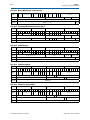
Table 1–1. IP Compiler for PCI Express Throughput
Link Width
×1
×2
×4
×8
PCI Express Gen1 Gbps (1.x compliant)
2
4
8
16
PCI Express Gen2 Gbps (2.0 compliant)
4
8
16
32
f Refer to the PCI Express High Performance Reference Design for bandwidth numbers
for the hard IP implementation in Stratix® IV GX and Arria® II GX devices.
Features
Altera’s IP Compiler for PCI Express offers extensive support across multiple device
families. It supports the following key features:
August 2014
■
Hard IP implementation—PCI Express Base Specification 1.1 or 2.0. The PCI Express
protocol stack including the transaction, data link, and physical layers is hardened
in the device.
■
Soft IP implementation:
■
PCI Express Base Specification 1.0a or 1.1.
■
Many device families supported. Refer to Table 1–4.
■
The PCI Express protocol stack including transaction, data link, and physical
layer is implemented using FPGA fabric logic elements
Altera Corporation
IP Compiler for PCI Express User Guide
1–2
Chapter 1: Datasheet
Features
■
Feature rich:
■
Support for ×1, ×2, ×4, and ×8 configurations. You can select the ×2 lane
configuration for the Cyclone® IV GX without down configuring a ×4
configuration.
■
Optional end-to-end cyclic redundancy code (ECRC) generation and checking
and advanced error reporting (AER) for high reliability applications.
■
Extensive maximum payload size support:
Stratix IV GX hard IP—Up to 2 KBytes (128, 256, 512, 1,024, or 2,048 bytes).
Arria II GX, Arria II GZ, and Cyclone IV GX hard IP—Up to 256 bytes (128 or
256 bytes).
Soft IP Implementations—Up to 2 KBytes (128, 256, 512, 1,024, or 2,048 bytes).
■
Easy to use:
■
Easy parameterization.
■
Substantial on-chip resource savings and guaranteed timing closure using the
IP Compiler for PCI Express hard IP implementation.
■
Easy adoption with no license requirement for the hard IP implementation.
■
Example designs to get started.
■
Qsys support.
■
Stratix V support is provided by the Stratix V Hard IP for PCI Express.
■
Stratix V support is not available with the IP Compiler for PCI Express.
■
The Stratix V Hard IP for PCI Express is documented in the Stratix V Hard
IP for PCI Express User Guide.
Different features are available for the soft and hard IP implementations and for the
three possible design flows. Table 1–2 outlines these different features.
Table 1–2. IP Compiler for PCI Express Features (Part 1 of 2)
Feature
Hard IP
Soft IP
MegaCore License
Free
Required
Root port
Not supported
Not supported
Gen1
×1, ×2, ×4, ×8
×1, ×4
Gen2
×1, ×4
No
Avalon Memory-Mapped (Avalon-MM)
Interface
Supported
Supported
64-bit Avalon Streaming (Avalon-ST) Interface Not supported
Not supported
128-bit Avalon-ST Interface
Not supported
Not supported
Descriptor/Data Interface (1)
Not supported
Not supported
Legacy Endpoint
Not supported
Not supported
IP Compiler for PCI Express User Guide
August 2014 Altera Corporation
Chapter 1: Datasheet
Release Information
1–3
Table 1–2. IP Compiler for PCI Express Features (Part 2 of 2)
Feature
Hard IP
Transaction layer packet type (TLP) (2)
Soft IP
■
Memory read
request
■
Memory write
request
■
Completion with
or without data
■
Memory read request
■
Memory write
request
■
Completion with or
without data
Maximum payload size
128–256 bytes
128–256 bytes
Number of virtual channels
1
1
Reordering of out–of–order completions
(transparent to the application layer)
Supported
Supported
Requests that cross 4 KByte address
Supported
boundary (transparent to the application layer)
Supported
Number of tags supported for non-posted
requests
16
16
ECRC forwarding on RX and TX
Not supported
Not supported
MSI-X
Not supported
Not supported
Notes to Table 1–2:
(1) Not recommended for new designs.
(2) Refer to Appendix A, Transaction Layer Packet (TLP) Header Formats for the layout of TLP headers.
Release Information
Table 1–3 provides information about this release of the IP Compiler for PCI Express.
Table 1–3. IP Compiler for PCI Express Release Information
Item
Version
Release Date
Ordering Codes
Description
14.0
June 2014
IP-PCIE/1
IP-PCIE/4
IP-PCIE/8
IP-AGX-PCIE/1
IP-AGX-PCIE/4
No ordering code is required for the hard IP implementation.
Product IDs
■
Hard IP Implementation
■
Soft IP Implementation
FFFF
×1–00A9
×4–00AA
×8–00AB
Vendor ID
August 2014
■
Hard IP Implementation
6AF7
■
Soft IP Implementation
6A66
Altera Corporation
IP Compiler for PCI Express
1–4
Chapter 1: Datasheet
Device Family Support
Altera verifies that the current version of the Quartus® II software compiles the
previous version of each IP core. Any exceptions to this verification are reported in the
MegaCore IP Library Release Notes and Errata. Altera does not verify compilation with
IP core versions older than one release.Table 1–4 shows the level of support offered by
the IP Compiler for PCI Express for each Altera device family.
Device Family Support
Table 1–4. Device Family Support
Device Family
Support (1)
Arria II GX
Final
Arria II GZ
Final
Cyclone IV GX
Final
Stratix IV E, GX
Final
Stratix IV GT
Final
Other device families
No support
Note to Table 1–4:
(1) Refer to the What's New for IP in Quartus II page for device support level information.
f In the Quartus II 11.0 release, support for Stratix V devices is offered with the Stratix V
Hard IP for PCI Express, and not with the IP Compiler for PCI Express. For more
information, refer to the Stratix V Hard IP for PCI Express User Guide .
General Description
The IP Compiler for PCI Express generates customized variations you use to design
PCI Express root ports or endpoints, including non-transparent bridges, or truly
unique designs combining multiple IP Compiler for PCI Express variations in a single
Altera device. The IP Compiler for PCI Express implements all required and most
optional features of the PCI Express specification for the transaction, data link, and
physical layers.
IP Compiler for PCI Express User Guide
August 2014 Altera Corporation
Chapter 1: Datasheet
General Description
1–5
The hard IP implementation includes all of the required and most of the optional
features of the specification for the transaction, data link, and physical layers.
Depending upon the device you choose, one to four instances of the IP Compiler for
PCI Express hard implementation are available. These instances can be configured to
include any combination of root port and endpoint designs to meet your system
requirements. A single device can also use instances of both the soft and hard
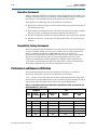
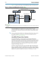
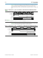
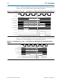
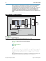
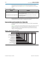
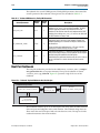
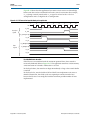
implementations of the IP Compiler for PCI Express. Figure 1–1 provides a high-level
block diagram of the hard IP implementation.
Figure 1–1. IP Compiler for PCI Express Hard IP Implementation High-Level Block Diagram (Note 1) (2)
FPGA Fabric
PCIe Hard IP Block
Transceivers
PIPE Interface
PCI Express
Protocol Stack
PMA
PCS
Retry
Buffer
TL
Interface
Virtual
Channel
RX
Buffer
Adapter
LMI
PCIe
Reconfig
FPGA Fabric Interface
Clock & Reset
Selection
Application
Layer
Test, Debug &
Configuration
Logic
PCIe Hard IP Block Reconfiguration
Notes to Figure 1–1:
(1) Stratix IV GX devices have two virtual channels.
(2) LMI stands for Local Management Interface.
This user guide includes a design example and testbench that you can configure as a
root port (RP) or endpoint (EP). You can use these design examples as a starting point
to create and test your own root port and endpoint designs.
f The purpose of the IP Compiler for PCI Express User Guide is to explain how to use the
IP Compiler for PCI Express and not to explain the PCI Express protocol. Although
there is inevitable overlap between the two documents, this document should be used
in conjunction with an understanding of the following PCI Express specifications:
PHY Interface for the PCI Express Architecture PCI Express 3.0 and PCI Express Base
Specification 1.0a, 1.1, or 2.0.
Support for IP Compiler for PCI Express Hard IP
If you target an Arria II GX, Arria II GZ, Cyclone IV GX, or Stratix IV GX device, you
can parameterize the IP core to include a full hard IP implementation of the PCI
Express stack including the following layers:
August 2014
■
Physical (PHY)
■
Physical Media Attachment (PMA)
Altera Corporation
IP Compiler for PCI Express
1–6
Chapter 1: Datasheet
General Description
■
Physical Coding Sublayer (PCS)
■
Media Access Control (MAC)
■
Data link
■
Transaction
Optimized for Altera devices, the hard IP implementation supports all memory, I/O,
configuration, and message transactions. The IP cores have a highly optimized
application interface to achieve maximum effective throughput. Because the compiler
is parameterizeable, you can customize the IP cores to meet your design
requirements.Table 1–5 lists the configurations that are available for the IP Compiler
for PCI Express hard IP implementation.
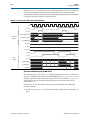
Table 1–5. Hard IP Configurations for the IP Compiler for PCI Express in Quartus II Software Version 11.0
Device
Link Rate (Gbps)
×1
×2 (1)
×4
×8
Avalon Streaming (Avalon-ST) Interface
Arria II GX
Arria II GZ
Cyclone IV GX
Stratix IV GX
2.5
yes
no
yes
yes (2)
5.0
no
no
no
no
2.5
yes
no
yes
yes (2)
5.0
yes
no
yes (2)
no
2.5
yes
yes
yes
no
5.0
no
no
no
no
2.5
yes
no
yes
yes
5.0
yes
no
yes
yes
Avalon-MM Interface using Qsys Design Flow (3)
Arria II GX
2.5
yes
no
yes
no
Cyclone IV GX
2.5
yes
yes
yes
no
2.5
yes
no
yes
yes
5.0
yes
no
yes
no
Stratix IV GX
Notes to Table 1–5:
(1) For devices that do not offer a ×2 initial configuration, you can use a ×4 configuration with the upper two lanes left unconnected at the device
pins. The link will negotiate to ×2 if the attached device is ×2 native or capable of negotiating to ×2.
(2) The ×8 support uses a 128-bit bus at 125 MHz.
(3) The Qsys design flow supports the generation of endpoint variations only.
Table 1–6 lists the Total RX buffer space, Retry buffer size, and Maximum Payload
size for device families that include the hard IP implementation. You can find these
parameters on the Buffer Setup page of the parameter editor.
Table 1–6. IP Compiler for PCI Express Buffer and Payload Information (Part 1 of 2)
Devices Family
Arria II GX
IP Compiler for PCI Express User Guide
Total RX Buffer Space
Retry Buffer
Max Payload Size
4 KBytes
2 KBytes
256 Bytes
August 2014 Altera Corporation
Chapter 1: Datasheet
General Description
1–7
Table 1–6. IP Compiler for PCI Express Buffer and Payload Information (Part 2 of 2)
Devices Family
Total RX Buffer Space
Retry Buffer
Max Payload Size
Arria II GZ
16 KBytes
16 KBytes
2 KBytes
Cyclone IV GX
4 KBytes
2 KBytes
256 Bytes
Stratix IV GX
16 KBytes
16 KBytes
2 KBytes
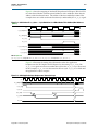
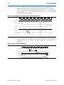
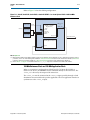
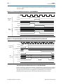
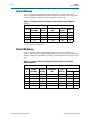
The IP Compiler for PCI Express supports ×1, ×2, ×4, and ×8 variations (Table 1–7 on
page 1–8) that are suitable for either root port or endpoint applications. You can use
the parameter editor to customize the IP core. The Qsys design flows do not support
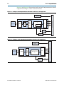
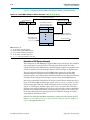
root port variations. Figure 1–2 shows a relatively simple application that includes
two IP Compilers for PCI Express, one configured as a root port and the other as an
endpoint.
Figure 1–2. PCI Express Application with a Single Root Port and Endpoint
Altera FPGA with Embedded
PCIe Hard IP Block
Altera FPGA with Embedded
PCIe Hard IP Block
PCIe
Hard IP
Block
User Application
Logic
August 2014
Altera Corporation
PCIe
Hard IP
Block
PCI Express Link
RP
EP
User Application
Logic
IP Compiler for PCI Express
1–8
Chapter 1: Datasheet
General Description
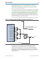
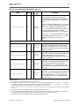
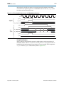
Figure 1–3 illustrates a heterogeneous topology, including an Altera device with two
PCIe hard IP root ports. One root port connects directly to a second FPGA that
includes an endpoint implemented using the hard IP IP core. The second root port
connects to a switch that multiplexes among three PCI Express endpoints.
Figure 1–3. PCI Express Application with Two Root Ports
Altera FPGA with Embedded PCIe
Hard IP Blocks
Altera FPGA with Embedded PCIe
Hard IP Blocks
PCIe
Hard IP
Block
PCIe
Hard IP
Block
User Application
Logic
RP
PCIe Link
User Application
Logic
EP
PCIe Link
PCIe Hard IP Block
Switch
RP
IP Compiler
for
PCI Express
Soft IP
Implementation
PCIe Link
User Application
Logic
EP
PCIe Link
PCIe Hard IP Block
EP
Altera FPGA Supporting IP Compiler for
PCI Express Soft IP Implementation
User Application
Logic
PIPE
Interface
PCIe Link
IP Compiler
for
PCI Express
Soft IP
Implementation
PHY
Altera FPGA with Embedded PCIe
Hard IP Blocks
User
Application
Logic
If you target a device that includes an internal transceiver, you can parameterize the
IP Compiler for PCI Express to include a complete PHY layer, including the MAC,
PCS, and PMA layers. If you target other device architectures, the IP Compiler for PCI
Express generates the IP core with the Intel-designed PIPE interface, making the IP
core usable with other PIPE-compliant external PHY devices.
Table 1–7 lists the protocol support for devices that include HSSI transceivers.
Table 1–7. Operation in Devices with HSSI Transceivers (Part 1 of 2) (Note 1)
Device Family
×1
×4
×8
Stratix IV GX hard IP–Gen1
Yes
Yes
Yes
Stratix IV GX hard IP–Gen 2
Yes (2)
Yes (2)
Yes (3)
Stratix IV soft IP–Gen1
Yes
Yes
No
Cyclone IV GX hard IP–Gen1
Yes
Yes
No
IP Compiler for PCI Express User Guide
August 2014 Altera Corporation
Chapter 1: Datasheet
IP Core Verification
1–9
Table 1–7. Operation in Devices with HSSI Transceivers (Part 2 of 2) (Note 1)
Device Family
×1
×4
×8
Arria II GX–Gen1 Hard IP Implementation
Yes
Yes
Yes
Arria II GX–Gen1 Soft IP Implementation
Yes
Yes
No
Arria II GZ–Gen1 Hard IP Implementation
Yes
Yes
Yes
Arria II GZ–Gen2 Hard IP Implementation
Yes
Yes
No
Notes to Table 1–7:
(1) Refer to Table 1–2 on page 1–2 for a list of features available in the different implementations and design flows.
(2) Not available in -4 speed grade. Requires -2 or -3 speed grade.
(3) Gen2 ×8 is only available in the -2 and I3 speed grades.
1
The device names and part numbers for Altera FPGAs that include internal
transceivers always include the letters GX, GT, or GZ. If you select a device that does
not include an internal transceiver, you can use the PIPE interface to connect to an
external PHY. Table 3–9 on page 3–8 lists the available external PHY types.
You can customize the payload size, buffer sizes, and configuration space (base
address registers support and other registers). Additionally, the IP Compiler for PCI
Express supports end-to-end cyclic redundancy code (ECRC) and advanced error
reporting for ×1, ×2, ×4, and ×8 configurations.
External PHY Support
Altera IP Compiler for PCI Express variations support a wide range of PHYs,
including the TI XIO1100 PHY in 8-bit DDR/SDR mode or 16-bit SDR mode; NXP
PX1011A for 8-bit SDR mode, a serial PHY, and a range of custom PHYs using
8-bit/16-bit SDR with or without source synchronous transmit clock modes and 8-bit
DDR with or without source synchronous transmit clock modes. You can constrain TX
I/Os by turning on the Fast Output Enable Register option in the parameter editor,
or by editing this setting in the Quartus II Settings File (.qsf). This constraint ensures
fastest tCO timing.
Debug Features
The IP Compiler for PCI Express also includes debug features that allow observation
and control of the IP cores for faster debugging of system-level problems.
f For more information about debugging refer to Chapter 17, Debugging.
IP Core Verification
To ensure compliance with the PCI Express specification, Altera performs extensive
validation of the IP Compiler for PCI Express. Validation includes both simulation
and hardware testing.
August 2014
Altera Corporation
IP Compiler for PCI Express
1–10
Chapter 1: Datasheet
Performance and Resource Utilization
Simulation Environment
Altera’s verification simulation environment for the IP Compiler for PCI Express uses
multiple testbenches that consist of industry-standard BFMs driving the PCI Express
link interface. A custom BFM connects to the application-side interface.
Altera performs the following tests in the simulation environment:
■
Directed tests that test all types and sizes of transaction layer packets and all bits of
the configuration space
■
Error injection tests that inject errors in the link, transaction layer packets, and data
link layer packets, and check for the proper response from the IP cores
■
PCI-SIG® Compliance Checklist tests that specifically test the items in the checklist
■
Random tests that test a wide range of traffic patterns across one or more virtual
channels
Compatibility Testing Environment
Altera has performed significant hardware testing of the IP Compiler for PCI Express
to ensure a reliable solution. The IP cores have been tested at various PCI-SIG PCI
Express Compliance Workshops in 2005–2009 with Arria GX, Arria II GX,
Cyclone IV GX, Stratix II GX, and Stratix IV GX devices and various external PHYs.
They have passed all PCI-SIG gold tests and interoperability tests with a wide
selection of motherboards and test equipment. In addition, Altera internally tests
every release with motherboards and switch chips from a variety of manufacturers.
All PCI-SIG compliance tests are also run with each IP core release.
Performance and Resource Utilization
The hard IP implementation of the IP Compiler for PCI Express is available in
Arria II GX, Arria II GZ, Cyclone IV GX, and Stratix IV GX devices.
Table 1–8 shows the resource utilization for the hard IP implementation using either
the Avalon-ST or Avalon-MM interface with a maximum payload of 256 bytes and 32
tags for the Avalon-ST interface and 16 tags for the Avalon-MM interface.
Table 1–8. Performance and Resource Utilization in Arria II GX, Arria II GZ, Cyclone IV GX, and
Stratix IV GX Devices (Part 1 of 2)
Parameters
Lane
Width
Internal
Clock (MHz)
Size
Virtual
Channel
Combinational
ALUTs
Dedicated
Registers
Memory Blocks
M9K
Avalon-ST Interface
×1
125
1
100
100
0
×1
125
2
100
100
0
×4
125
1
200
200
0
×4
125
2
200
200
0
×8
250
1
200
200
0
×8
250
2
200
200
0
IP Compiler for PCI Express User Guide
August 2014 Altera Corporation
Chapter 1: Datasheet
Recommended Speed Grades
1–11
Table 1–8. Performance and Resource Utilization in Arria II GX, Arria II GZ, Cyclone IV GX, and
Stratix IV GX Devices (Part 2 of 2)
Parameters
Size
Lane
Width
Internal
Clock (MHz)
Virtual
Channel
×4
125
1
Combinational
ALUTs
Dedicated
Registers
Memory Blocks
M9K
Avalon-MM Interface–Qsys Design Flow
×1
125
1
×4
125
1
×8
250
1
1600
1600
18
Avalon-MM Interface–Qsys Design Flow - Completer Only
×1
125
1
×4
125
1
1000
1150
10
Avalon-MM Interface–Qsys Design Flow - Completer Only Single Dword
×1
125
1
×4
125
1
×4
250
1
430
450
0
Note to Table 1–8:
(1) The transaction layer of the Avalon-MM implementation is implemented in programmable logic to improve latency.
f Refer to Appendix C, Performance and Resource Utilization Soft IP Implementation
for performance and resource utilization for the soft IP implementation.
Recommended Speed Grades
Table 1–9 shows the recommended speed grades for each device family for the
supported link widths and internal clock frequencies. For soft IP implementations of
the IP Compiler for PCI Express, the table lists speed grades that are likely to meet
timing; it may be possible to close timing in a slower speed grade. For the hard IP
implementation, the speed grades listed are the only speed grades that close timing.
When the internal clock frequency is 125 MHz or 250 MHz, Altera recommends
setting the Quartus II Analysis & Synthesis Settings Optimization Technique to
Speed.
August 2014
Altera Corporation
IP Compiler for PCI Express
1–12
Chapter 1: Datasheet
Recommended Speed Grades
f Refer to “Setting Up and Running Analysis and Synthesis” in Quartus II Help and
Area and Timing Optimization in volume 2 of the Quartus II Handbook for more
information about how to effect this setting.
Table 1–9. Recommended Device Family Speed Grades (Part 1 of 2)
Device Family
Link Width
Internal Clock
Frequency (MHz)
Recommended
Speed Grades
Avalon-ST Hard IP Implementation
Arria II GX Gen1 with ECC Support (1)
Arria II GZ Gen1 with ECC Support
Arria II GZ Gen 2 with ECC Support
Cyclone IV GX Gen1 with ECC Support
Stratix IV GX Gen1 with ECC Support (1)
Stratix IV GX Gen2 with ECC Support (1)
Stratix IV GX Gen2 without ECC Support
×1
62.5 (2)
–4,–5,–6
×1
125
–4,–5,–6
×4
125
–4,–5,–6
×8
125
–4,–5,–6
×1
125
-3, -4
×4
125
-3, -4
×8
125
-3, -4
×1
125
-3
×4
125
-3
×1
62.5 (2)
all speed grades
125
all speed grades
×1, ×2, ×4
×1
62.5 (2)
–2, –3 (3)
×1
125
–2, –3, –4
×4
125
–2, –3, –4
×8
250
–2, –3, –4 (3)
×1
125
–2, –3 (3)
×4
250
–2, –3 (3)
×8
500
–2, I3 (4)
×1, ×4
125
–6
×1, ×2, ×4
125
–6, –7
×1
62.5
–6, –7, –8
×1, ×4
125
–2, –3, –4
×8
250
–2, –3
×1
125
–2, –3
×4
250
–2, –3
Avalon–MM Interface–Qsys Flow
Arria II GX
Cyclone IV GX
Stratix IV GX Gen1
Stratix IV GX Gen2
Avalon-ST or Descriptor/Data Interface Soft IP Implementation
Arria II GX
×1, ×4
125
–4. –5 (5)
Cyclone IV GX
×1
125
–6, –7 (5)
×1
62.5
all speed grades
×1, ×4
125
all speed grades
Stratix IV E Gen1
IP Compiler for PCI Express User Guide
August 2014 Altera Corporation
Chapter 1: Datasheet
Recommended Speed Grades
1–13
Table 1–9. Recommended Device Family Speed Grades (Part 2 of 2)
Internal Clock
Frequency (MHz)
Recommended
Speed Grades
×1
62.5
all speed grades
×4
125
all speed grades
Device Family
Stratix IV GX Gen1
Link Width
Notes to Table 1–9:
(1) The RX Buffer and Retry Buffer ECC options are only available in the hard IP implementation.
(2) This is a power-saving mode of operation.
(3) Final results pending characterization by Altera for speed grades -2, -3, and -4. Refer to the .fit.rpt file generated
by the Quartus II software.
(4) Closing timing for the –3 speed grades in the provided endpoint example design requires seed sweeping.
(5) You must turn on the following Physical Synthesis settings in the Quartus II Fitter Settings to achieve timing
closure for these speed grades and variations: Perform physical synthesis for combinational logic, Perform
register duplication, and Perform register retiming. In addition, you can use the Quartus II Design Space
Explorer or Quartus II seed sweeping methodology. Refer to the Netlist Optimizations and Physical Synthesis
chapter in volume 2 of the Quartus II Handbook for more information about how to set these options.
(6) Altera recommends disabling the OpenCore Plus feature for the ×8 soft IP implementation because including this
feature makes it more difficult to close timing.
August 2014
Altera Corporation
IP Compiler for PCI Express
1–14
IP Compiler for PCI Express User Guide
Chapter 1: Datasheet
Recommended Speed Grades
August 2014 Altera Corporation
2. Getting Started
August 2014
<edit Part Number variable in chapter>
This section provides step-by-step instructions to help you quickly set up and
simulate the IP Compiler for PCI Express testbench. The IP Compiler for PCI Express
provides numerous configuration options. The parameters chosen in this chapter are
the same as those chosen in the PCI Express High-Performance Reference Design
available on the Altera website.
Installing and Licensing IP Cores
The Altera IP Library provides many useful IP core functions for production use
without purchasing an additional license. You can evaluate any Altera IP core in
simulation and compilation in the Quartus II software using the OpenCore evaluation
feature.
Some Altera IP cores, such as MegaCore® functions, require that you purchase a
separate license for production use. You can use the OpenCore Plus feature to
evaluate IP that requires purchase of an additional license until you are satisfied with
the functionality and performance. After you purchase a license, visit the Self Service
Licensing Center to obtain a license number for any Altera product. For additional
information, refer to Altera Software Installation and Licensing.
Figure 2–1. IP core Installation Path
acds
quartus - Contains the Quartus II software
ip - Contains the Altera IP Library and third-party IP cores
altera - Contains the Altera IP Library source code
<IP core name> - Contains the IP core source files
1
The default installation directory on Windows is <drive>:\altera\<version number>;
on Linux it is <home directory>/altera/<version number>.
OpenCore Plus IP Evaluation
Altera's free OpenCore Plus feature allows you to evaluate licensed MegaCore IP
cores in simulation and hardware before purchase. You need only purchase a license
for MegaCore IP cores if you decide to take your design to production. OpenCore Plus
supports the following evaluations:
■
Simulate the behavior of a licensed IP core in your system.
■
Verify the functionality, size, and speed of the IP core quickly and easily.
■
Generate time-limited device programming files for designs that include IP cores.
■
Program a device with your IP core and verify your design in hardware
OpenCore Plus evaluation supports the following two operation modes:
■
August 2014
Untethered—run the design containing the licensed IP for a limited time.
Altera Corporation
IP Compiler for PCI Express User Guide
2–2
Chapter 2: Getting Started
IP Catalog and Parameter Editor
■
Tethered—run the design containing the licensed IP for a longer time or
indefinitely. This requires a connection between your board and the host
computer.
All IP cores that use OpenCore Plus time out simultaneously when any IP core in the
design times out.
IP Catalog and Parameter Editor
The Quartus II IP Catalog (Tools > IP Catalog) and parameter editor help you easily
customize and integrate IP cores into your project. You can use the IP Catalog and
parameter editor to select, customize, and generate files representing your custom IP
variation.
1
The IP Catalog (Tools > IP Catalog) and parameter editor replace the MegaWizard™
Plug-In Manager for IP selection and parameterization, beginning in Quartus II
software version 14.0. Use the IP Catalog and parameter editor to locate and
paramaterize Altera IP cores.
The IP Catalog lists IP cores available for your design. Double-click any IP core to
launch the parameter editor and generate files representing your IP variation. The
parameter editor prompts you to specify an IP variation name, optional ports, and
output file generation options. The parameter editor generates a top level Qsys
system file (.qsys) or Quartus II IP file (.qip) representing the IP core in your project.
You can also parameterize an IP variation without an open project.
Use the following features to help you quickly locate and select an IP core:
■
Filter IP Catalog to Show IP for active device family or Show IP for all device
families.
■
Search to locate any full or partial IP core name in IP Catalog. Click Search for
Partner IP, to access partner IP information on the Altera website.
IP Compiler for PCI Express User Guide
August 2014 Altera Corporation
Chapter 2: Getting Started
IP Catalog and Parameter Editor
■
2–3
Right-click an IP core name in IP Catalog to display details about supported
devices, installation location, and links to documentation.
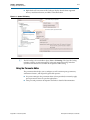
Figure 2–2. Quartus II IP Catalog
Search and filter IP for your target device
Double-click to customize, right-click for information
1
The IP Catalog is also available in Qsys (View > IP Catalog). The Qsys IP Catalog
includes exclusive system interconnect, video and image processing, and other
system-level IP that are not available in the Quartus II IP Catalog.
Using the Parameter Editor
The parameter editor helps you to configure your IP variation ports, parameters,
architecture features, and output file generation options:
August 2014
■
Use preset settings in the parameter editor (where provided) to instantly apply
preset parameter values for specific applications.
■
View port and parameter descriptions and links to detailed documentation.
Altera Corporation
IP Compiler for PCI Express User Guide
2–4
Chapter 2: Getting Started
Upgrading Outdated IP Cores
■
Generate testbench systems or example designs (where provided).
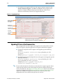
Figure 2–3. IP Parameter Editors
View IP port
and parameter
details
Legacy parameter
editors
Specify your IP variation name
and target device
Apply preset parameters for
specific applications
Modifying an IP Variation
You can easily modify the parameters of any Altera IP core variation in the parameter
editor to match your design requirements. Use any of the following methods to
modify an IP variation in the parameter editor.
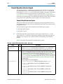
Table 2–1. Modifying an IP Variation
Menu Command
Action
File > Open
Select the top-levelHDL(.v, or .vhd) IP variation file to
launch the parameter editor and modify the IP variation.
Regenerate the IP variation to implement your changes.
View > Utility Windows >
Project Navigator > IP Components
Double-click the IP variation to launch the parameter
editor and modify the IP variation. Regenerate the IP
variation to implement your changes.
Project > Upgrade IP Components
Select the IP variation and click Upgrade in Editor to
launch the parameter editor and modify the IP variation.
Regenerate the IP variation to implement your changes.
Upgrading Outdated IP Cores
IP core variants generated with a previous version of the Quartus II software may
require upgrading before use in the current version of the Quartus II software. Click
Project > Upgrade IP Components to identify and upgrade IP core variants.
The Upgrade IP Components dialog box provides instructions when IP upgrade is
required, optional, or unsupported for specific IP cores in your design. You must
upgrade IP cores that require it before you can compile the IP variation in the current
version of the Quartus II software. Many Altera IP cores support automatic upgrade.
IP Compiler for PCI Express User Guide
August 2014 Altera Corporation
Chapter 2: Getting Started
Upgrading Outdated IP Cores
2–5
The upgrade process renames and preserves the existing variation file (.v, .sv, or .vhd)
as <my_ip>_ BAK.v, .sv, .vhd in the project directory.
Table 2–2. IP Core Upgrade Status
IP Core Status
Corrective Action
Required Upgrade IP
Components
You must upgrade the IP variation before compiling in the current
version of the Quartus II software.
Optional Upgrade IP
Components
Upgrade is optional for this IP variation in the current version of the
Quartus II software. You can upgrade this IP variation to take
advantage of the latest development of this IP core. Alternatively you
can retain previous IP core characteristics by declining to upgrade.
Upgrade Unsupported
Upgrade of the IP variation is not supported in the current version of
the Quartus II software due to IP core end of life or incompatibility
with the current version of the Quartus II software. You are prompted
to replace the obsolete IP core with a current equivalent IP core from
the IP Catalog.
Before you begin
■
Archive the Quartus II project containing outdated IP cores in the original version
of the Quartus II software: Click Project > Archive Project to save the project in
your previous version of the Quartus II software. This archive preserves your
original design source and project files.
■
Restore the archived project in the latest version of the Quartus II software: Click
Project > Restore Archived Project. Click OK if prompted to change to a
supported device or overwrite the project database. File paths in the archive must
be relative to the project directory. File paths in the archive must reference the IP
variation .v or .vhd file or .qsys file (not the .qip file).
1. In the latest version of the Quartus II software, open the Quartus II project
containing an outdated IP core variation. The Upgrade IP Components dialog
automatically displays the status of IP cores in your project, along with
instructions for upgrading each core. Click Project > Upgrade IP Components to
access this dialog box manually.
August 2014
Altera Corporation
IP Compiler for PCI Express User Guide
2–6
Chapter 2: Getting Started
Upgrading Outdated IP Cores
2. To simultaneously upgrade all IP cores that support automatic upgrade, click
Perform Automatic Upgrade. The Status and Version columns update when
upgrade is complete. Example designs provided with any Altera IP core
regenerate automatically whenever you upgrade the IP core.
Figure 2–4. Upgrading IP Cores
Displays upgrade
status for all IP cores
in the Project
Double-click to
individually migrate
Checked IP cores
support “Auto Upgrade”
Successful
“Auto Upgrade”
Upgrade
unavailable
Upgrades all IP core that support “Auto Upgrade”
Upgrades individual IP cores unsupported by “Auto Upgrade”
Upgrading IP Cores at the Command Line
You can upgrade IP cores that support auto upgrade at the command line. IP cores
that do not support automatic upgrade do not support command line upgrade.
■
To upgrade a single IP core that supports auto-upgrade, type the following
command:
quartus_sh –ip_upgrade –variation_files <my_ip_filepath/my_ip>.<hdl>
<qii_project>
Example: quartus_sh -ip_upgrade -variation_files mega/pll25.v hps_testx
■
To simultaneously upgrade multiple IP cores that support auto-upgrade, type the
following command:
quartus_sh –ip_upgrade –variation_files “<my_ip_filepath/my_ip1>.<hdl>;
<my_ip_filepath/my_ip2>.<hdl>” <qii_project>
Example: quartus_sh -ip_upgrade -variation_files
"mega/pll_tx2.v;mega/pll3.v" hps_testx
f IP cores older than Quartus II software version 12.0 do not support upgrade. Altera
verifies that the current version of the Quartus II software compiles the previous
version of each IP core. The MegaCore IP Library Release Notes reports any verification
exceptions for MegaCore IP. The Quartus II Software and Device Support Release Notes
reports any verification exceptions for other IP cores. Altera does not verify
compilation for IP cores older than the previous two releases.
IP Compiler for PCI Express User Guide
August 2014 Altera Corporation
Chapter 2: Getting Started
Parameterizing the IP Compiler for PCI Express
2–7
Parameterizing the IP Compiler for PCI Express
This section guides you through the process of parameterizing the IP Compiler for
PCI Express as an endpoint, using the same options that are chosen in Chapter 15,
Testbench and Design Example. Complete the following steps to specify the
parameters:
1. In the IP Catalog (Tools > IP Catalog), locate and double-click the name of the IP
core to customize. The parameter editor appears.
2. Specify a top-level name for your custom IP variation. This name identifies the IP
core variation files in your project. For this walkthrough, specify top.v for the
name of the IP core file: <working_dir>\top.v.
3. Specify the following values in the parameter editor:
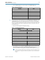
Table 2–3. System Settings Parameters
Parameter
Value
PCIe Core Type
PHY type
PHY interface
Configure transceiver block
Lanes
Xcvr ref_clk
Application interface
Port type
PCI Express version
Application clock
Max rate
Test out width
HIP reconfig
PCI Express hard IP
Stratix IV GX
serial
Use default settings.
×8
100 MHz
Avalon-ST 128 -bit
Native Endpoint
2.0
250 MHz
Gen 2 (5.0 Gbps)
64 bits
Disable
4. To enable all of the tests in the provided testbench and chaining DMA example
design, make the base address register (BAR) assignments. Bar2 or Bar3 is
required.Table 2–4. provides the BAR assignments in tabular format.
Table 2–4. PCI Registers (Part 1 of 2)
PCI Base Registers (Type 0 Configuration Space)
BAR
BAR TYPE
BAR Size
0
32-Bit Non-Prefetchable Memory
256 MBytes - 28 bits
1
32-Bit Non-Prefetchable Memory
256 KBytes - 18 bits
2
32-bit Non-Prefetchable Memory
256 KBytes -18 bits
PCI Read-Only Registers
Register Name
Device ID
0xE001
Subsystem ID
0x2801
Revision ID
Vendor ID
August 2014
Value
Altera Corporation
0x01
0x1172
IP Compiler for PCI Express User Guide
2–8
Chapter 2: Getting Started
Parameterizing the IP Compiler for PCI Express
Table 2–4. PCI Registers (Part 2 of 2)
PCI Base Registers (Type 0 Configuration Space)
Subsystem vendor ID
0x5BDE
Class code
0xFF0000
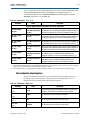
5. Specify the following settings for the Capabilities parameters.
Table 2–5. Capabilities Parameters
Parameter
Value
Device Capabilities
Tags supported
32
Implement completion timeout disable
Turn this option On
Completion timeout range
ABCD
Error Reporting
Implement advanced error reporting
Off
Implement ECRC check
Off
Implement ECRC generation
Off
Implement ECRC forwarding
Off
MSI Capabilities
MSI messages requested
4
MSI message 64–bit address capable
On
Link Capabilities
Link common clock
On
Data link layer active reporting
Off
Surprise down reporting
Off
Link port number
0x01
Slot Capabilities
Enable slot capability
Off
Slot capability register
0x0000000
MSI-X Capabilities
Implement MSI-X
Off
Table size
0x000
Offset
0x00000000
BAR indicator (BIR)
0
Pending Bit Array (PBA)
Offset
0x00000000
BAR Indicator
0
IP Compiler for PCI Express User Guide
August 2014 Altera Corporation
Chapter 2: Getting Started
Parameterizing the IP Compiler for PCI Express
2–9
6. Click the Buffer Setup tab to specify settings on the Buffer Setup page.
Table 2–6. Buffer Setup Parameters
Parameter
1
Value
Maximum payload size
512 bytes
Number of virtual channels
1
Number of low-priority VCs
None
Auto configure retry buffer size
On
Retry buffer size
16 KBytes
Maximum retry packets
64
Desired performance for received requests
Maximum
Desired performance for received completions
Maximum
For the PCI Express hard IP implementation, the RX Buffer Space Allocation is fixed
at Maximum performance. This setting determines the values for a read-only table
that lists the number of posted header credits, posted data credits, non-posted header
credits, completion header credits, completion data credits, total header credits, and
total RX buffer space.
7. Specify the following power management settings.
Table 2–7. Power Management Parameters
Parameter
Value
L0s Active State Power Management (ASPM)
Idle threshold for L0s entry
8,192 ns
Endpoint L0s acceptable latency
< 64 ns
Number of fast training sequences (N_FTS)
Common clock
Gen2: 255
Separate clock
Gen2: 255
Electrical idle exit (EIE) before FTS
4
L1s Active State Power Management (ASPM)
Enable L1 ASPM
Off
Endpoint L1 acceptable latency
< 1 µs
L1 Exit Latency Common clock
> 64 µs
L1 Exit Latency Separate clock
> 64 µs
8. On the EDA tab, turn on Generate simulation model to generate an IP functional
simulation model for the IP core. An IP functional simulation model is a
cycle-accurate VHDL or Verilog HDL model produced by the Quartus II software.
c
August 2014
Altera Corporation
Use the simulation models only for simulation and not for synthesis or any
other purposes. Using these models for synthesis creates a non-functional
design.
IP Compiler for PCI Express User Guide
2–10
Chapter 2: Getting Started
Viewing the Generated Files
9. On the Summary tab, select the files you want to generate. A gray checkmark
indicates a file that is automatically generated. All other files are optional.
10. Click Finish to generate the IP core, testbench, and supporting files.
1
A report file, <variation name>.html, in your project directory lists each file
generated and provides a description of its contents.
Viewing the Generated Files
Figure 2–5 illustrates the directory structure created for this design after you generate
the IP Compiler for PCI Express. The directories includes the following files:
■
The IP Compiler for PCI Express design files, stored in <working_dir>.
■
The chaining DMA design example file, stored in the
<working_dir>\top_examples\chaining_dma directory. This design example tests
your generated IP Compiler for PCI Express variation. For detailed information
about this design example, refer to Chapter 15, Testbench and Design Example.
■
The simulation files for the chaining DMA design example, stored in the
<working_dir>\top_examples\chaining_dma\testbench directory. The Quartus II
software generates the testbench files if you turn on Generate simulation model
on the EDA tab while generating the IP Compiler for PCI Express.
0
Figure 2–5. Directory Structure for IP Compiler for PCI Express and Testbench
IP Compiler for
PCI Express
Files
<working_dir>
<variation>.v = top.v, the parameterized PCI Express IP Core
<variation>.sdc = top.sdc, the timing constraints file
<variation>.tcl = top.tcl, general Quartus II settings
ip_compiler_for_pci_express-library
contains local copy of the pci express library files needed for
simulation, or compilation, or both
<variation>_examples = top_examples
Simulation and
Quartus II
Compilation
common
Includes testbench and incremental compile directories
Testbench and
Design Example
Files
chaining_dma, files to implement the chaining DMA
top_example_chaining_top.qpf, the Quartus II project file
top_example_chaining_top.qsf, the Quartus II settings file
<variation>_plus.v = top_plus.v,
the parameterized PCI Express IP Core including reset and
calibration circuitry
(1) (2)
testbench, scripts to run the testbench
runtb.do, script to run the testbench
<variation>_chaining_testbench = top_chaining_testbench.v
altpcietb_bfm_driver_chaining.v , provides test stimulus
Notes to Figure 2–5:
(1) The chaining_dma directory contains the Quartus II project and settings files.
(2) <variation>_plus.v is only available for the hard IP implementation.
IP Compiler for PCI Express User Guide
August 2014 Altera Corporation
Chapter 2: Getting Started
Viewing the Generated Files
2–11
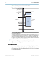
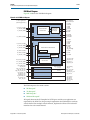
Figure 2–6 illustrates the top-level modules of this design. As this figure illustrates,
the IP Compiler for PCI Express connects to a basic root port bus functional model
(BFM) and an application layer high-performance DMA engine. These two modules,
when combined with the IP Compiler for PCI Express, comprise the complete
example design. The test stimulus is contained in altpcietb_bfm_driver_chaining.v.
The script to run the tests is runtb.do. For a detailed explanation of this example
design, refer to Chapter 15, Testbench and Design Example.
Figure 2–6. Testbench for the Chaining DMA Design Example
Root Port BFM
Root Port Driver
x8 Root Port Model
PCI Express Link
Endpoint Example
IP Compiler
for PCI Express
Endpoint Application
Layer Example
Traffic Control/Virtual Channel Mapping
Request/Completion Routing
RC
Slave
(Optional)
DMA
Write
DMA
Read
Endpoint
Memory
(32 KBytes)
f The design files used in this design example are the same files that are used for the
PCI Express High-Performance Reference Design. You can download the required
files on the PCI Express High-Performance Reference Design product page. This
product page includes design files for various devices. The example in this document
uses the Stratix IV GX files. You can generate, simulate, and compile the design
example with the files and capabilities provided in your Quartus II software and IP
installation. However, to configure the example on a device, you must also download
altpcie_demo.zip, which includes a software driver that the example design uses,
from the PCI Express High-Performance Reference Design.
August 2014
Altera Corporation
IP Compiler for PCI Express User Guide
2–12
Chapter 2: Getting Started
Simulating the Design
The Stratix IV .zip file includes files for Gen1 and Gen2 ×1, ×4, and ×8 variants. The
example in this document demonstrates the Gen2 ×8 variant. After you download
and unzip this .zip file, you can copy the files for this variant to your project directory,
<working_dir>. The files for the example in this document are included in the
hip_s4gx_gen2x8_128 directory. The Quartus II project file, top.qsf, is contained in
<working_dir>. You can use this project file as a reference for the .qsf file for your own
design.
Simulating the Design
As Figure 2–5 illustrates, the scripts to run the simulation files are located in the
<working_dir>\top_examples\chaining_dma\testbench directory. Follow these
steps to run the chaining DMA testbench.
1. Start your simulation tool. This example uses the ModelSim® software.
1
The endpoint chaining DMA design example DMA controller requires the
use of BAR2 or BAR3.
2. In the testbench directory,
<working_dir>\top_examples\chaining_dma\testbench, type the following
command:
do runtb.do r
This script compiles the testbench for simulation and runs the chaining DMA
tests.
Example 2–1 shows the partial transcript from a successful simulation. As this
transcript illustrates, the simulation includes the following stages:
■
Link training
■
Configuration
■
DMA reads and writes
IP Compiler for PCI Express User Guide
August 2014 Altera Corporation
Chapter 2: Getting Started
Simulating the Design
2–13
■
Root port to endpoint memory reads and writes
Example 2–1. Excerpts from Transcript of Successful Simulation Run
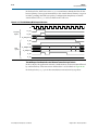
Time: 56000 Instance: top_chaining_testbench.ep.epmap.pll_250mhz_to_500mhz.
altpll_component.pll0
# INFO:
464 ns Completed initial configuration of Root Port.
# INFO: Core Clk Frequency: 251.00 Mhz
# INFO: 3608 ns EP LTSSM State: DETECT.ACTIVE
# INFO: 3644 ns EP LTSSM State: POLLING.ACTIVE
# INFO: 3660 ns RP LTSSM State: DETECT.ACTIVE
# INFO: 3692 ns RP LTSSM State: POLLING.ACTIVE
# INFO: 6012 ns RP LTSSM State: POLLING.CONFIG
# INFO: 6108 ns EP LTSSM State: POLLING.CONFIG
# INFO: 7388 ns EP LTSSM State: CONFIG.LINKWIDTH.START
# INFO: 7420 ns RP LTSSM State: CONFIG.LINKWIDTH.START
# INFO: 7900 ns EP LTSSM State: CONFIG.LINKWIDTH.ACCEPT
# INFO: 8316 ns RP LTSSM State: CONFIG.LINKWIDTH.ACCEPT
# INFO: 8508 ns RP LTSSM State: CONFIG.LANENUM.WAIT
# INFO: 9004 ns EP LTSSM State: CONFIG.LANENUM.WAIT
# INFO: 9196 ns EP LTSSM State: CONFIG.LANENUM.ACCEPT
# INFO: 9356 ns RP LTSSM State: CONFIG.LANENUM.ACCEPT
# INFO: 9548 ns RP LTSSM State: CONFIG.COMPLETE
# INFO: 9964 ns EP LTSSM State: CONFIG.COMPLETE
# INFO: 11052 ns EP LTSSM State: CONFIG.IDLE
# INFO: 11276 ns RP LTSSM State: CONFIG.IDLE
# INFO: 11356 ns RP LTSSM State: L0
# INFO: 11580 ns EP LTSSM State: L0
August 2014
Altera Corporation
IP Compiler for PCI Express User Guide
2–14
Chapter 2: Getting Started
Simulating the Design
Example 2-1 continued
## INFO: 12536 ns
# INFO: 15896 ns
EP PCI Express Link Status Register (1081):
# INFO: 15896 ns
Negotiated Link Width: x8
# INFO: 15896 ns
Slot Clock Config: System Reference Clock Used
# INFO: 16504 ns RP LTSSM State: RECOVERY.RCVRLOCK
# INFO: 16840 ns EP LTSSM State: RECOVERY.RCVRLOCK
# INFO: 17496 ns EP LTSSM State: RECOVERY.RCVRCFG
# INFO: 18328 ns RP LTSSM State: RECOVERY.RCVRCFG
# INFO: 20440 ns RP LTSSM State: RECOVERY.SPEED
# INFO: 20712 ns EP LTSSM State: RECOVERY.SPEED
# INFO: 21600 ns EP LTSSM State: RECOVERY.RCVRLOCK
# INFO: 21614 ns RP LTSSM State: RECOVERY.RCVRLOCK
# INFO: 22006 ns RP LTSSM State: RECOVERY.RCVRCFG
# INFO: 22052 ns EP LTSSM State: RECOVERY.RCVRCFG
# INFO: 22724 ns EP LTSSM State: RECOVERY.IDLE
# INFO: 22742 ns RP LTSSM State: RECOVERY.IDLE
# INFO: 22846 ns RP LTSSM State: L0
# INFO: 22900 ns EP LTSSM State: L0
# INFO: 23152 ns
Current Link Speed: 5.0GT/s
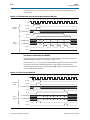
# INFO: 27936 ns --------# INFO: 27936 ns TASK:dma_set_header READ
# INFO: 27936 ns Writing Descriptor header
# INFO: 27976 ns data content of the DT header
# INFO: 27976 ns
# INFO: 27976 ns Shared Memory Data Display:
# INFO: 27976 ns Address Data
# INFO: 27976 ns ------- ---# INFO: 27976 ns 00000900 00000003 00000000 00000900 CAFEFADE
# INFO: 27976 ns --------# INFO: 27976 ns TASK:dma_set_rclast
# INFO: 27976 ns Start READ DMA : RC issues MWr (RCLast=0002)
# INFO: 27992 ns --------# INFO: 28000 ns TASK:msi_poll Polling MSI Address:07F0---> Data:FADE......
# INFO: 28092 ns TASK:rcmem_poll Polling RC Address0000090C
current data (0000FADE)
expected data (00000002)
# INFO: 29592 ns TASK:rcmem_poll Polling RC Address0000090C
current data (00000000)
expected data (00000002)
# INFO: 31392 ns TASK:rcmem_poll Polling RC Address0000090C
current data (00000002)
expected data (00000002)
# INFO: 31392 ns TASK:rcmem_poll ---> Received Expected Data (00000002)
# INFO: 31440 ns TASK:msi_poll
Received DMA Read MSI(0000) : B0FC
# INFO: 31448 ns Completed DMA Read
# INFO: 31448 ns --------# INFO: 31448 ns TASK:chained_dma_test
# INFO: 31448 ns
DMA: Write
# INFO: 31448 ns --------# INFO: 31448 ns TASK:dma_wr_test
# INFO: 31448 ns
DMA: Write
# INFO: 31448 ns --------# INFO: 31448 ns TASK:dma_set_wr_desc_data
# INFO: 31448 ns --------INFO: 31448 ns TASK:dma_set_msi WRITE
# INFO: 31448 ns Message Signaled Interrupt Configuration
# INFO: 1448 ns msi_address (RC memory)= 0x07F0
# INFO: 31760 ns msi_control_register = 0x00A5
# INFO: 32976 ns msi_expected = 0xB0FD
IP Compiler for PCI Express User Guide
August 2014 Altera Corporation
Chapter 2: Getting Started
Simulating the Design
2–15
Example 2-1 continued
# INFO: 32976 ns msi_capabilities address = 0x0050
# INFO: 32976 ns multi_message_enable = 0x0002
# INFO: 32976 ns msi_number = 0001
# INFO: 32976 ns msi_traffic_class = 0000
# INFO: 32976 ns --------# INFO: 26416 ns TASK:chained_dma_test
# INFO: 26416 ns
DMA: Read
# INFO: 26416 ns --------# INFO: 26416 ns TASK:dma_rd_test
# INFO: 26416 ns --------# INFO: 26416 ns TASK:dma_set_rd_desc_data
# INFO: 26416 ns --------# INFO: 26416 ns TASK:dma_set_msi READ
# INFO: 26416 ns Message Signaled Interrupt Configuration
# INFO: 26416 ns msi_address (RC memory)= 0x07F0
# INFO: 26720 ns msi_control_register = 0x0084
# INFO: 27936 ns msi_expected = 0xB0FC
# INFO: 27936 ns msi_capabilities address = 0x0050
# INFO: 27936 ns multi_message_enable = 0x0002
# INFO: 27936 ns msi_number = 0000
# INFO: 27936 ns
msi_traffic_class = 0000
# INFO: 32976 ns TASK:dma_set_header WRITE
# INFO: 32976 ns Writing Descriptor header
# INFO: 33016 ns data content of the DT header
# INFO: 33016 ns
# INFO: 33016 ns Shared Memory Data Display:
# INFO: 33016 ns Address Data
# INFO: 33016 ns ------- ---# INFO: 33016 ns 00000800 10100003 00000000 00000800 CAFEFADE
# INFO: 33016 ns --------# INFO: 33016 ns TASK:dma_set_rclast
# INFO: 33016 ns Start WRITE DMA : RC issues MWr (RCLast=0002)
# INFO: 33032 ns --------# INFO: 33038 ns TASK:msi_poll Polling MSI Address:07F0---> Data:FADE......
# INFO: 33130 ns TASK:rcmem_poll Polling RC Address0000080C
current data (0000FADE)
expected data (00000002)
# INFO: 34130 ns TASK:rcmem_poll Polling RC Address0000080C
current data (00000000)
expected data (00000002)
# INFO: 35910 ns TASK:msi_poll Received DMA Write MSI(0000) : B0FD
# INFO: 35930 ns TASK:rcmem_poll Polling RC Address0000080C
current data (00000002)
expected data (00000002)
# INFO: 35930 ns TASK:rcmem_poll ---> Received Expected Data (00000002)
# INFO: 35938 ns --------# INFO: 35938 ns Completed DMA Write
# INFO: 35938 ns --------# INFO: 35938 ns TASK:check_dma_data
# INFO: 35938 ns Passed : 0644 identical dwords.
# INFO: 35938 ns --------# INFO: 35938 ns TASK:downstream_loop
# INFO: 36386 ns Passed: 0004 same bytes in BFM mem addr 0x00000040 and 0x00000840
# INFO: 36826 ns Passed: 0008 same bytes in BFM mem addr 0x00000040 and 0x00000840
# INFO: 37266 ns Passed: 0012 same bytes in BFM mem addr 0x00000040 and 0x00000840
# INFO: 37714 ns Passed: 0016 same bytes in BFM mem addr 0x00000040 and 0x00000840
# INFO: 38162 ns Passed: 0020 same bytes in BFM mem addr 0x00000040 and 0x00000840
# INFO: 38618 ns Passed: 0024 same bytes in BFM mem addr 0x00000040 and 0x00000840
# INFO: 39074 ns Passed: 0028 same bytes in BFM mem addr 0x00000040 and 0x00000840
# INFO: 39538 ns Passed: 0032 same bytes in BFM mem addr 0x00000040 and 0x00000840
# INFO: 40010 ns Passed: 0036 same bytes in BFM mem addr 0x00000040 and 0x00000840
# INFO: 40482 ns Passed: 0040 same bytes in BFM mem addr 0x00000040 and 0x00000840
# SUCCESS: Simulation stopped due to successful completion!
August 2014
Altera Corporation
IP Compiler for PCI Express User Guide
2–16
Chapter 2: Getting Started
Constraining the Design
Constraining the Design
The Quartus project directory for the chaining DMA design example is in
<working_dir>\top_examples\chaining_dma\. Before compiling the design using
the Quartus II software, you must apply appropriate design constraints, such as
timing constraints. The Quartus II software automatically generates the constraint
files when you generate the IP Compiler for PCI Express.
Table 2–8 describes these constraint files.
Table 2–8. Automatically Generated Constraints Files
Constraint Type
Directory
Description
General
<working_dir>/<variation>.tcl (top.tcl)
This file includes various Quartus II constraints. In
particular, it includes virtual pin assignments. Virtual
pin assignments allow you to avoid making specific
pin assignments for top-level signals while you are
simulating and not yet ready to map the design to
hardware.
Timing
<working_dir>/<variation>.sdc (top.sdc)
This file is the Synopsys Design Constraints File (.sdc)
which includes timing constraints.
If you want to perform an initial compilation to check any potential issues without
creating pin assignments for a specific board, you can do so after running the
following two steps that constrain the chaining DMA design example:
1. To apply Quartus II constraint files, type the following commands at the Tcl
console command prompt:
source ../../top.tcl r
1
To display the Quartus II Tcl Console, on the View menu, point to Utility
Windows and click Tcl Console.
2. To add the Synopsys timing constraints to your design, follow these steps:
a. On the Assignments menu, click Settings.
b. Click TimeQuest Timing Analyzer.
c. Under SDC files to include in the project, click the Browse button. Browse to
your <working_dir> to add top.sdc.
d. Click Add.
e. Click OK.
IP Compiler for PCI Express User Guide
August 2014 Altera Corporation
Chapter 2: Getting Started
Constraining the Design
2–17
Example 2–2 illustrates the Synopsys timing constraints.
Example 2–2. Synopsys Timing Constraints
derive_pll_clocks
derive_clock_uncertainty
create_clock -period "100 MHz" -name {refclk} {refclk}
set_clock_groups -exclusive -group [get_clocks { refclk*clkout }] -group [get_clocks {
*div0*coreclkout}]
set_clock_groups -exclusive -group [get_clocks { *central_clk_div0* }] -group
[get_clocks { *_hssi_pcie_hip* }] -group [get_clocks { *central_clk_div1* }]
<The following 4 additional constraints are for Stratix IV ES Silicon only>
set_multicycle_path -from [get_registers *delay_reg*] -to [get_registers *all_one*] hold -start 1
set_multicycle_path -from [get_registers *delay_reg*] -to [get_registers *all_one*] setup -start 2
set_multicycle_path -from [get_registers *align*chk_cnt*] -to [get_registers
*align*chk_cnt*] -hold -start 1
set_multicycle_path -from [get_registers *align*chk_cnt*] -to [get_registers
*align*chk_cnt*] -setup -start 2
Specifying Device and Pin Assignments
If you want to download the design to a board, you must specify the device and pin
assignments for the chaining DMA example design. To make device and pin
assignments, follow these steps:
1. To select the device, on the Assignments menu, click Device.
2. In the Family list, select Stratix IV (GT/GX/E).
3. Scroll through the Available devices to select EP4SGX230KF40C2.
4. To add pin assignments for the EP4SGX230KF40C2 device, copy all the text
included in to the chaining DMA design example .qsf file,
<working_dir>\top_examples\chaining_dma\top_example_chaining_top.qsf to
your project .qsf file.
August 2014
Altera Corporation
IP Compiler for PCI Express User Guide
2–18
Chapter 2: Getting Started
Constraining the Design
1
The pin assignments provided in the .qsf are valid for the Stratix IV GX
FPGA Development Board and the EP4SGX230KF40C2 device. If you are
using different hardware you must determine the correct pin assignments.
Example 2–3. Pin Assignments for the Stratix IV GX (EP4SGX230KF40C2) FPGA Development Board
set_location_assignment
set_location_assignment
set_location_assignment
set_location_assignment
set_location_assignment
set_location_assignment
set_location_assignment
set_location_assignment
set_location_assignment
set_location_assignment
set_location_assignment
set_instance_assignment
set_location_assignment
set_location_assignment
set_location_assignment
set_location_assignment
set_location_assignment
set_location_assignment
set_location_assignment
set_location_assignment
set_location_assignment
set_location_assignment
set_location_assignment
set_location_assignment
set_location_assignment
set_location_assignment
set_location_assignment
set_location_assignment
set_location_assignment
set_location_assignment
set_location_assignment
set_location_assignment
set_location_assignment
set_location_assignment
set_location_assignment
set_instance_assignment
set_instance_assignment
set_instance_assignment
set_instance_assignment
set_instance_assignment
set_instance_assignment
set_instance_assignment
set_instance_assignment
set_instance_assignment
set_instance_assignment
set_instance_assignment
set_instance_assignment
set_instance_assignment
set_instance_assignment
set_instance_assignment
set_instance_assignment
set_instance_assignment
set_instance_assignment
set_instance_assignment
IP Compiler for PCI Express User Guide
PIN_AK35 -to local_rstn_ext
PIN_R32 -to pcie_rstn
PIN_AN38 -to refclk
PIN_AU38 -to rx_in0
PIN_AR38 -to rx_in1
PIN_AJ38 -to rx_in2
PIN_AG38 -to rx_in3
PIN_AE38 -to rx_in4
PIN_AC38 -to rx_in5
PIN_U38 -to rx_in6
PIN_R38 -to rx_in7
-name INPUT_TERMINATION DIFFERENTIAL -to free_100MHz -disable
PIN_AT36 -to tx_out0
PIN_AP36 -to tx_out1
PIN_AH36 -to tx_out2
PIN_AF36 -to tx_out3
PIN_AD36 -to tx_out4
PIN_AB36 -to tx_out5
PIN_T36 -to tx_out6
PIN_P36 -to tx_out7
PIN_AB28 -to gen2_led
PIN_F33 -to L0_led
PIN_AK33 -to alive_led
PIN_W28 -to comp_led
PIN_R29 -to lane_active_led[0]
PIN_AH35 -to lane_active_led[2]
PIN_AE29 -to lane_active_led[3]
PIN_AL35 -to usr_sw[0]
PIN_AC35 -to usr_sw[1]
PIN_J34 -to usr_sw[2]
PIN_AN35 -to usr_sw[3]
PIN_G33 -to usr_sw[4]
PIN_K35 -to usr_sw[5]
PIN_AG34 -to usr_sw[6]
PIN_AG31 -to usr_sw[7]
-name IO_STANDARD "2.5 V" -to local_rstn_ext
-name IO_STANDARD "2.5 V" -to pcie_rstn
-name INPUT_TERMINATION OFF -to refclk
-name IO_STANDARD "1.4-V PCML" -to rx_in0
-name IO_STANDARD "1.4-V PCML" -to rx_in1
-name IO_STANDARD "1.4-V PCML" -to rx_in2
-name IO_STANDARD "1.4-V PCML" -to rx_in3
-name IO_STANDARD "1.4-V PCML" -to rx_in4
-name IO_STANDARD "1.4-V PCML" -to rx_in5
-name IO_STANDARD "1.4-V PCML" -to rx_in6
-name IO_STANDARD "1.4-V PCML" -to rx_in7
-name IO_STANDARD "1.4-V PCML" -to tx_out0
-name IO_STANDARD "1.4-V PCML" -to tx_out1
-name IO_STANDARD "1.4-V PCML" -to tx_out2
-name IO_STANDARD "1.4-V PCML" -to tx_out3
-name IO_STANDARD "1.4-V PCML" -to tx_out4
-name IO_STANDARD "1.4-V PCML" -to tx_out5
-name IO_STANDARD "1.4-V PCML" -to tx_out6
-name IO_STANDARD "1.4-V PCML" -to tx_out7
August 2014 Altera Corporation
Chapter 2: Getting Started
Compiling the Design
2–19
Pin Assignments for the Stratix IV (EP4SGX230KF40C2) Development Board (continued)
set_instance_assignment -name IO_STANDARD "2.5 V" -to usr_sw[0]
set_instance_assignment -name IO_STANDARD "2.5 V" -to usr_sw[1]
set_instance_assignment -name IO_STANDARD "2.5 V" -to usr_sw[2]
set_instance_assignment -name IO_STANDARD "2.5 V" -to usr_sw[3]
set_instance_assignment -name IO_STANDARD "2.5 V" -to usr_sw[4]
set_instance_assignment -name IO_STANDARD "2.5 V" -to usr_sw[5]
set_instance_assignment -name IO_STANDARD "2.5 V" -to usr_sw[6]
set_instance_assignment -name IO_STANDARD "2.5 V" -to usr_sw[7]
set_instance_assignment -name IO_STANDARD "2.5 V" -to
lane_active_led[0]
set_instance_assignment -name IO_STANDARD "2.5 V" -to
lane_active_led[2]
set_instance_assignment -name IO_STANDARD "2.5 V" -to
lane_active_led[3]
set_instance_assignment -name IO_STANDARD "2.5 V" -to L0_led
set_instance_assignment -name IO_STANDARD "2.5 V" -to alive_led
set_instance_assignment -name IO_STANDARD "2.5 V" -to comp_led
# Note reclk_free uses 100 MHz input
# On the S4GX Dev kit make sure that
#
SW4.5 = ON
#
SW4.6 = ON
set_instance_assignment -name IO_STANDARD LVDS -to free_100MHz
set_location_assignment PIN_AV22 -to free_100MHz
Specifying QSF Constraints
This section describes two additional constraints to improve performance in specific
cases.
■
Constraints for Stratix IV GX ES silicon–add the following constraint to your .qsf
file:
set_instance_assignment -name GLOBAL_SIGNAL "GLOBAL CLOCK" -to
*wire_central_clk_div*_coreclkout
This constraint aligns the PIPE clocks (core_clk_out) from each quad to reduce
clock skew in ×8 variants.
■
Constraints for design running at frequencies higher than 250 MHz:
set_global_assignment -name PHYSICAL_SYNTHESIS_ASYNCHRONOUS_SIGNAL_PIPELINING ON
This constraint improves performance for designs in which asynchronous signals
in very fast clock domains cannot be distributed across the FPGA fast enough due
to long global network delays. This optimization performs automatic pipelining of
these signals, while attempting to minimize the total number of registers inserted.
Compiling the Design
To test your IP Compiler for PCI Express in hardware, your initial Quartus II
compilation includes all of the directories shown in Figure 2–5. After you have fully
tested your customized design, you can exclude the testbench directory from the
Quartus II compilation.
On the Processing menu, click Start Compilation to compile your design.
August 2014
Altera Corporation
IP Compiler for PCI Express User Guide
2–20
Chapter 2: Getting Started
Reusing the Example Design
Reusing the Example Design
To use this example design as the basis of your own design, replace the endpoint
application layer example shown in Figure 2–6 with your own application layer
design. Then, modify the BFM driver to generate the transactions needed to test your
application layer.
IP Compiler for PCI Express User Guide
August 2014 Altera Corporation
3. Parameter Settings
August 2014
<edit Part Number variable in chapter>
You customize the IP Compiler for PCI Express by specifying parameters in the IP
Compiler for PCI Express parameter editor, which you access from the IP Catalog.
Some IP Compiler for PCI Express variations are supported in only one or two of the
design flows. Soft IP implementations are supported only in the Quartus II IP Catalog.
For more information about the hard IP implementation variations available in the
different design flows, refer to Table 1–5 on page 1–6.
This chapter describes the parameters and how they affect the behavior of the IP core.
The IP Compiler for PCI Express parameter editor that appears in the Qsys flow is
different from the IP Compiler for PCI Express parameter editor that appears in the
other two design flows. Because the Qsys design flow supports only a subset of the
variations supported in the other two flows, and generates only hard IP
implementations with specific characteristics, the Qsys flow parameter editor
supports only a subset of the parameters described in this chapter.
Parameters in the Qsys Design Flow
The following sections describe the IP Compiler for PCI Express parameters available
in the Qsys design flow. Separate sections describe the parameters available in
different sections of the IP Compiler for PCI Express parameter editor.
The available parameters reflect the fact that the Qsys design flow supports only the
following functionality:
August 2014
■
Hard IP implementation
■
Native endpoint, with no support for:
■
I/O space BAR
■
32-bit prefetchable memory
■
16 Tags
■
1 Message Signaled Interrupt (MSI)
■
1 virtual channel
■
Up to 256 bytes maximum payload
Altera Corporation
IP Compiler for PCI Express User Guide
3–2
Chapter 3: Parameter Settings
Parameters in the Qsys Design Flow
System Settings
The first parameter section of the IP Compiler for PCI Express parameter editor in the
Qsys flow contains the parameters for the overall system settings. Table 3–1 describes
these settings.
Table 3–1. Qsys Flow System Settings Parameters
Parameter
Value
Description
Gen2 Lane Rate Mode Off/On
Specifies the maximum data rate at which the link can operate. Turning
on Gen2 Lane Rate Mode sets the Gen2 rate, and turning it off sets the
Gen1 rate. Refer to Table 1–5 on page 1–6 for a complete list of Gen1
and Gen2 support.
Number of Lanes
×1, ×2, ×4, ×8
Specifies the maximum number of lanes supported. Refer to Table 1–5
on page 1–6 for a complete list of device support for numbers of lanes.
Reference clock
frequency
100 MHz, 125 MHz
You can select either a 100 MHz or 125 MHz reference clock for Gen1
operation; Gen2 requires a 100 MHz clock.
Use 62.5 MHz
application clock
Off/On
Specifies whether the application interface clock operates at the slower
62.5 MHz frequency to support power saving. This parameter can only
be turned on for some Gen1 ×1 variations. Refer to Table 4–1 on
page 4–4 for a list of the supported application interface clock
frequencies in different device families.
Test out width
Indicates the width of the test_out signal. Most of these signals are
None, 9 bits, or 64 bits reserved. Refer to Table 5–33 on page 5–59 for more information.
Altera recommends that you configure the 64-bit width.
PCI Base Address Registers
The ×1 and ×4 IP cores support memory space BARs ranging in size from 128 bytes to
the maximum allowed by a 32-bit or 64-bit BAR. The ×8 IP cores support memory
space BARs from 4 KBytes to the maximum allowed by a 32-bit or 64-bit BAR.
The available BARs reflect the fact that the Qsys design flow supports only native
endpoints, with no support for I/O space BARs or 32-bit prefetchable memory.
The Avalon-MM address is the translated base address corresponding to a BAR hit of
a received request from the PCI Express link.
In the Qsys design flow, the PCI Base Address Registers (Type 0 Configuration
Space) Bar Size and Avalon Base Address information populates from Qsys. You
cannot enter this information in the IP Compiler for PCI Express parameter editor.
After you set the base addresses in Qsys, either automatically or by entering them
manually, the values appear when you reopen the parameter editor.
Altera recommends using the Qsys option—on the System menu, click Assign Base
Addresses—to set the base addresses automatically. If you decide to enter the address
translation entries manually, then you must avoid conflicts in address assignment
when adding other components, making interconnections, and assigning base
addresses.
IP Compiler for PCI Express User Guide
August 2014 Altera Corporation
Chapter 3: Parameter Settings
Parameters in the Qsys Design Flow
3–3
Table 3–2 describes the PCI register parameters. You can configure a BAR with value
other than Not used only if the preceding BARs are configured. When an
even-numbered BAR is set to 64 bit Prefetchable, the following BAR is labelled
Occupied and forced to value Not used.
Table 3–2. PCI Registers
(Note 1), (2)
Parameter
Value
Description
PCI Base Address Registers (0x10, 0x14, 0x18, 0x1C, 0x20, 0x24)
BAR Table (BAR0)
BAR Type
64 bit Prefetchable
BAR0 size and type mapping (memory space). BAR0 and BAR1 can
32 but Non-Prefetchable be combined to form a 64-bit prefetchable BAR. BAR0 and BAR1 can
Not used
be configured separately as 32-bit non-prefetchable memories.) (2)
BAR Table (BAR1)
BAR Type
BAR1 size and type mapping (memory space). BAR0 and BAR1 can
32 but Non-Prefetchable
be combined to form a 64-bit prefetchable BAR. BAR0 and BAR1 can
Not used
be configured separately as 32-bit non-prefetchable memories.)
BAR Table (BAR2)
BAR Type
64 bit Prefetchable
BAR2 size and type mapping (memory space). BAR2 and BAR3 can
32 but Non-Prefetchable be combined to form a 64-bit prefetchable BAR. BAR2 and BAR3 can
Not used
be configured separately as 32-bit non-prefetchable memories.) (2)
BAR Table (BAR3)
BAR Type
BAR3 size and type mapping (memory space). BAR2 and BAR3 can
32 but Non-Prefetchable
be combined to form a 64-bit prefetchable BAR. BAR2 and BAR3 can
Not used
be configured separately as 32-bit non-prefetchable memories.)
BAR Table (BAR4)
BAR Type
64 bit Prefetchable
BAR4 size and type mapping (memory space). BAR4 and BAR5 can
32 but Non-Prefetchable be combined to form a 64-bit BAR. BAR4 and BAR5 can be
Not used
configured separately as 32-bit non-prefetchable memories.) (2)
BAR Table (BAR5)
BAR Type
BAR5 size and type mapping (memory space). BAR4 and BAR5 can
32 but Non-Prefetchable
be combined to form a 64-bit BAR. BAR4 and BAR5 can be
Not used
configured separately as 32-bit non-prefetchable memories.)
Notes to Table 3–2:
(1) A prefetchable 64-bit BAR is supported. A non-prefetchable 64-bit BAR is not supported because in a typical system, the root port configuration
register of type 1 sets the maximum non-prefetchable memory window to 32-bits.
(2) The Qsys design flow does not support I/O space for BAR type mapping. I/O space is only supported for legacy endpoint port types.
Device Identification Registers
The device identification registers are part of the PCI Type 0 configuration space
header. You can set these register values only at device configuration. Table 3–3
describes the PCI read-only device identification registers.
Table 3–3. PCI Registers (Part 1 of 2)
Parameter
Vendor ID
0x000
Device ID
0x000
Revision ID
0x008
Class code
0x008
August 2014
Altera Corporation
Value
Description
0x1172
Sets the read-only value of the vendor ID register. This parameter
can not be set to 0xFFFF per the PCI Express Specification.
0x0004
Sets the read-only value of the device ID register.
0x01
Sets the read-only value of the revision ID register.
0xFF0000
Sets the read-only value of the class code register.
IP Compiler for PCI Express User Guide
3–4
Chapter 3: Parameter Settings
Parameters in the Qsys Design Flow
Table 3–3. PCI Registers (Part 2 of 2)
Subsystem ID
0x02C
Subsystem vendor ID
0x02C
0x0004
Sets the read-only value of the subsystem device ID register.
0x1172
Sets the read-only value of the subsystem vendor ID register. This
parameter can not be set to 0xFFFF per the PCI Express Base
Specification 1.1 or 2.0.
Link Capabilities
Table 3–4 describes the capabilities parameter available in the Link Capabilities
section of the IP Compiler for PCI Express parameter editor in the Qsys design flow.
Table 3–4. Link Capabilities Parameter
Parameter
Link port number
Value
Description
Sets the read-only value of the port number field in the link
capabilities register. (offset 0x08C in the PCI Express capability
structure or PCI Express Capability List register).
1
Error Reporting
The parameters in the Error Reporting section control settings in the PCI Express
advanced error reporting extended capability structure, at byte offsets 0x800 through
0x834. Table 3–5 describes the error reporting parameters available in the Qsys design
flow.
Table 3–5. Error Reporting Capabilities Parameters
Parameter
Value
Description
Implement
advanced error
reporting
On/Off
Implements the advanced error reporting (AER) capability.
Implement ECRC
check
On/Off
Enables ECRC checking capability. Sets the read-only value of the ECRC check
capable bit in the advanced error capabilities and control register. This parameter
requires you to implement the advanced error reporting capability.
Implement ECRC
generation
On/Off
Enables ECRC generation capability. Sets the read-only value of the ECRC generation
capable bit in the advanced error capabilities and control register. This parameter
requires you to implement the advanced error reporting capability.
IP Compiler for PCI Express User Guide
August 2014 Altera Corporation
Chapter 3: Parameter Settings
Parameters in the Qsys Design Flow
3–5
Buffer Configuration
The Buffer Configuration section of the IP Compiler for PCI Express parameter editor
in the Qsys design flow includes parameters for the receive and retry buffers. The IP
Compiler for PCI Express parameter editor also displays the read-only RX buffer
space allocation information. Table 3–6 describes the parameters and information in
this section of the parameter editor in the Qsys design flow.
Table 3–6. Buffer Configuration Parameters
Parameter
Maximum
payload size
0x084
RX buffer credit
allocation –
performance for
received requests
Value
128 bytes,
256 bytes
Description
Specifies the maximum payload size supported. This parameter sets the read-only
value of the max payload size supported field of the device capabilities register
(0x084[2:0]) and optimizes the IP core for this size payload. Maximum payload size
is 128 bytes or 256 bytes, depending on the device.
Low—Provides the minimal amount of space for desired traffic. Select this option
when the throughput of the received requests is not critical to the system design.
This setting minimizes the device resource utilization.
Maximum,
High,
Medium, Low
Because the Arria II GX and Stratix IV hard IP implementations have a fixed RX
Buffer size, the only available value for these devices is Maximum.
Note that the read-only values for header and data credits update as you change
this setting.
For more information, refer to Chapter 11, Flow Control.
These values show the credits and space allocated for each flow-controllable type,
based on the RX buffer size setting. All virtual channels use the same RX buffer
space allocation.
Posted header
credit
Posted data credit
Non-posted
header credit
Read-only
entries
Completion
header credit
Completion data
credit
August 2014
Altera Corporation
The entries show header and data credits for RX posted (memory writes) and
completion requests, and header credits for non-posted requests (memory reads).
The table does not show non-posted data credits because the IP core always
advertises infinite non-posted data credits and automatically has room for the
maximum number of dwords of data that can be associated with each non-posted
header.
The numbers shown for completion headers and completion data indicate how much
space is reserved in the RX buffer for completions. However, infinite completion
credits are advertised on the PCI Express link as is required for endpoints. The
application layer must manage the rate of non-posted requests to ensure that the RX
buffer completion space does not overflow. The hard IP RX buffer is fixed at 16
KBytes for Stratix IV GX devices and 4 KBytes for Arria II GX devices.
IP Compiler for PCI Express User Guide
3–6
Chapter 3: Parameter Settings
Parameters in the Qsys Design Flow
Avalon-MM Settings
The Avalon-MM Settings section of the Qsys design flow IP Compiler for PCI
Express parameter editor contains configuration settings for the PCI Express
Avalon-MM bridge. Table 3–7 describes these parameters.
Table 3–7. Avalon-MM Configuration Settings
Parameter
Value
Description
Specifies whether the IP Compiler for PCI Express component is
capable of sending requests to the upstream PCI Express devices, and
whether the incoming requests are pipelined.
Requester/Completer,
Peripheral Mode
Completer-Only,
Completer-Only
single dword
Requester/Completer—Enables the IP Compiler for PCI Express to
send request packets on the PCI Express TX link as well as receiving
request packets on the PCI Express RX link.
Completer-Only—In this mode, the IP Compiler for PCI Express
can receive requests, but cannot initiate upstream requests.
However, it can transmit completion packets on the PCI Express TX
link. This mode removes the Avalon-MM TX slave port and thereby
reduces logic utilization.
Completer-Only single dword—Non-pipelined version of
Completer-Only mode. At any time, only a single request can be
outstanding. Completer-Only single dword uses fewer resources
than Completer-Only.
Control Register Access
(CRA) Avalon slave port
(Qsys flow)
Auto Enable PCIe
Interrupt (enabled at
power-on)
Off/On
Allows read/write access to bridge registers from the Avalon
interconnect fabric using a specialized slave port. Disabling this option
disallows read/write access to bridge registers, except in the
Completer-Only single dword variations.
Off/On
Turning this option on enables the IP Compiler for PCI Express
interrupt register at power-up. Turning it off disables the interrupt
register at power-up. The setting does not affect run-time
configurability of the interrupt enable register.
IP Compiler for PCI Express User Guide
August 2014 Altera Corporation
Chapter 3: Parameter Settings
Parameters in the Qsys Design Flow
3–7
Address Translation
The Address Translation section of the Qsys design flow IP Compiler for PCI Express
parameter editor contains parameter settings for address translation in the PCI
Express Avalon-MM bridge. Table 3–8 describes these parameters.
Table 3–8. Avalon-MM Address Translation Settings
Parameter
Value
Description
Sets Avalon-MM-to-PCI Express address translation scheme to
dynamic or fixed.
Dynamic translation
table,
Fixed translation
table
Address Translation
Table Configuration
Dynamic translation table—Enables application software to write
the address translation table contents using the control register
access slave port. On-chip memory stores the table. Requires that
the Avalon-MM CRA Port be enabled. Use several address
translation table entries to avoid updating a table entry before
outstanding requests complete. This option supports up to 512
address pages.
Fixed translation table—Configures the address translation table
contents to hardwired fixed values at the time of system generation.
This option supports up to 16 address pages.
Number of address
pages
1, 2, 4, 8, 16, 32, 64,
128, 256, 512
Specifies the number of PCI Express base address pages of memory
that the bridge can access. This value corresponds to the number of
entries in the address translation table. The Avalon address range is
segmented into one or more equal-sized pages that are individually
mapped to PCI Express addresses. Select the number and size of the
address pages. If you select Dynamic translation table, use several
address translation table entries to avoid updating a table entry before
outstanding requests complete. Dynamic translation table supports up
to 512 address pages, and fixed translation table supports up to 16
address pages.
Size of address pages
4 Kbyte–4 Gbytes
Specifies the size of each PCI Express memory segment accessible by
the bridge. This value is common for all address translation entries.
Address Translation Table Contents
The address translation table in the Qsys design flow IP Compiler for PCI Express
parameter editor is valid only for the fixed translation table configuration. The table
provides information for translating Avalon-MM addresses to PCI Express addresses.
The number of address pages available in the table is the number of address pages
you specify in the Address Translation section of the parameter editor.
The table entries specify the PCI Express base addresses of memory that the bridge
can access. In translation of Avalon-MM addresses to PCI Express addresses, the
upper bits of the Avalon-MM address are replaced with part of a specific entry. The
most significant bits of the Avalon-MM address index the table, selecting the address
page to use for each request.
The PCIe address field comprises two parameters, bits [31:0] and bits [63:32] of the
address. The Size of address pages value you specify in the Address Translation
section of the parameter editor determines the number of least significant bits in the
address that are replaced by the lower bits of the incoming Avalon-MM address.
August 2014
Altera Corporation
IP Compiler for PCI Express User Guide
3–8
Chapter 3: Parameter Settings
IP Core Parameters
However, bit 0 of PCIe Address 31:0 has the following special significance:
■
If bit 0 of PCIe Address 31:0 has value 0, the PCI Express memory accessed
through this address page is 32-bit addressable.
■
If bit 0 of PCIe Address 31:0 has value 1, the PCI Express memory accessed
through this address page is 64-bit addressable.
IP Core Parameters
The following sections describe the IP Compiler for PCI Express parameters
System Settings
The first page of the Parameter Settings tab contains the parameters for the overall
system settings. Table 3–9 describes these settings.
The IP Compiler for PCI Express parameter editor that appears in the Qsys flow
provides only the Gen2 Lane Rate Mode, Number of lanes, Reference clock
frequency, Use 62.5 MHz application clock, and Test out width system settings
parameters. For more information, refer to “Parameters in the Qsys Design Flow” on
page 3–1.
Table 3–9. System Settings Parameters (Part 1 of 4)
Parameter
PCIe Core Type
Value
Hard IP for PCI Express
Soft IP for PCI Express
Description
The hard IP implementation uses embedded dedicated logic to
implement the PCI Express protocol stack, including the physical layer,
data link layer, and transaction layer.
The soft IP implementation uses optimized PLD logic to implement the
PCI Express protocol stack, including physical layer, data link layer, and
transaction layer.
The Qsys design flows support only the hard IP implementation.
IP Compiler for PCI Express User Guide
August 2014 Altera Corporation
Chapter 3: Parameter Settings
IP Core Parameters
3–9
Table 3–9. System Settings Parameters (Part 2 of 4)
Parameter
Value
Description
PCIe System Parameters
PHY type (1)
August 2014
Custom
Allows all types of external PHY interfaces (except serial). The number of
lanes can be ×1 or ×4. This option is only available for the soft IP
implementation.
Stratix II GX
Serial interface where Stratix II GX uses the Stratix II GX device family's
built-in transceiver. Selecting this PHY allows only a serial PHY interface
with the lane configuration set to Gen1 ×1, ×4, or ×8.
Stratix IV GX
Serial interface where Stratix IV GX uses the Stratix IV GX device
family's built-in transceiver to support PCI Express Gen1 and Gen2 ×1,
×4, and ×8. For designs that may target HardCopy IV GX, the
HardCopy IV GX setting must be used even when initially compiling for
Stratix IV GX devices. This procedure ensures that you only apply
HardCopy IV GX compatible settings in the Stratix IV GX
implementation.
Cyclone IV GX
Serial interface where Cyclone IV GX uses the Cyclone IV GX device
family’s built-in transceiver. Selecting this PHY allows only a serial PHY
interface with the lane configuration set to Gen1 ×1, ×2, or ×4.
HardCopy IV GX
Serial interface where HardCopy IV GX uses the HardCopy IV GX device
family's built-in transceiver to support PCI Express Gen1 and Gen2 ×1,
×4, and ×8. For designs that may target HardCopy IV GX, the
HardCopy IV GX setting must be used even when initially compiling for
Stratix IV GX devices. This procedure ensures HardCopy IV GX
compatible settings in the Stratix IV GX implementation. For Gen2 ×8
variations, this procedure will set the RX Buffer and Retry Buffer to be
only 8 KBytes which is the HardCopy IV GX compatible implementation.
Arria GX
Serial interface where Arria GX uses the Arria GX device family’s built-in
transceiver. Selecting this PHY allows only a serial PHY interface with
the lane configuration set to Gen1 ×1 or ×4.
Arria II GX
Serial interface where Arria II GX uses the Arria II GX device family's
built-in transceiver to support PCI Express Gen1 ×1, ×4, and ×8.
Arria II GZ
Serial interface where Arria II GZ uses the Arria II GZ device family's
built-in transceiver to support PCI Express Gen1 ×1, ×4, and ×8, Gen2
×1, Gen2 ×4.
TI XIO1100
TI XIO1100 uses an 8-bit DDR/SDR with a TXClk or a 16-bit SDR with a
transmit clock PHY interface. Both of these options restrict the number
of lanes to ×1. This option is only available for the soft IP
implementation.
NXP PX1011A
Philips NPX1011A uses an 8-bit SDR with a TXClk and a PHY interface.
This option restricts the number of lanes to ×1. This option is only
available for the soft IP implementation.
Altera Corporation
IP Compiler for PCI Express User Guide
3–10
Chapter 3: Parameter Settings
IP Core Parameters
Table 3–9. System Settings Parameters (Part 3 of 4)
Parameter
PHY interface
Value
16-bit SDR,
16-bit SDR w/TxClk,
8-bit DDR,
8-bit DDR w/TxClk,
8-bit DDR/SDR
w/TXClk,
8 bit SDR,
8-bit SDR w/TxClk,
serial
Description
Selects the specific type of external PHY interface based on the interface
datapath width and clocking mode. Refer to Chapter 14, External PHYs
for additional detail on specific PHY modes.
The PHY interface setting only applies to the soft IP implementation.
Clicking this button brings up the transceiver parameter editor, allowing
you to access a much greater subset of the transceiver parameters than
was available in earlier releases. The parameters that you can access are
different for the soft and hard IP versions of the IP Compiler for PCI
Express and may change from release to release. (2)
Configure transceiver
block
For Arria II GX, Cyclone IV GX, Stratix II GX, and Stratix IV GX
transceivers, refer to the “Protocol Settings for PCI Express (PIPE)” in
the ALTGX Transceiver Setup Guide for an explanation of these settings.
Lanes
Xcvr ref_clk
PHY pclk
×1, ×2, ×4, ×8
100 MHz, 125 MHz
Specifies the maximum number of lanes supported. The ×8 soft IP
configuration is only supported for Stratix II GX devices. For information
about ×8 support in hard IP configurations, refer to Table 1–5 on
page 1–6.
For Arria II GX, Cyclone IV GX, HardCopy IV GX, and Stratix IV GX, you
can select either a 100 MHz or 125 MHz reference clock for Gen1
operation; Gen2 requires a 100 MHz clock. The Arria GX and
Stratix II GX devices require a 100 MHz clock. If you use a PIPE
interface (and the PHY type is not Arria GX, Arria II GX, Cyclone IV GX,
HardCopy IV GX, Stratix II GX, or Stratix IV GX) the refclk is not
required.
For Custom and TI X101100 PHYs, the PHY pclk frequency is 125 MHz.
For the NXP PX1011A PHY, the pclk value is 250 MHz.
Application Interface
Port type
PCI Express version
64-bit Avalon-ST,
128-bit Avalon-ST,
Descriptor/Data,
Avalon-MM
Native Endpoint
Legacy Endpoint
Root Port
1.0A, 1.1, 2.0
IP Compiler for PCI Express User Guide
Specifies the interface between the PCI Express transaction layer and the
application layer. When using the parameter editor, this parameter can
be set to Avalon-ST or Descriptor/Data. Altera recommends the AvalonST option for all new designs. 128-bit Avalon-ST is only available when
using the hard IP implementation.
Specifies the port type. Altera recommends Native Endpoint for all new
endpoint designs. Select Legacy Endpoint only when you require I/O
transaction support for compatibility. The Qsys design flow only
supports Native Endpoint and the Avalon-MM interface to the user
application. The Root Port option is available in the hard IP
implementations.
The endpoint stores parameters in the Type 0 configuration space which
is outlined in Table 6–2 on page 6–2. The root port stores parameters in
the Type 1 configuration space which is outlined in Table 6–3 on
page 6–3.
Selects the PCI Express specification with which the variation is
compatible. Depending on the device that you select, the IP Compiler for
PCI Express hard IP implementation supports PCI Express versions 1.1
and 2.0. The IP Compiler for PCI Express soft IP implementation
supports PCI Express versions 1.0a and 1.1
August 2014 Altera Corporation
Chapter 3: Parameter Settings
IP Core Parameters
3–11
Table 3–9. System Settings Parameters (Part 4 of 4)
Parameter
Value
Specifies the frequency at which the application interface clock operates.
This frequency can only be set to 62.5 MHz or 125 MHz for some Gen1
×1 variations. For all other variations this field displays the frequency of
operation which is controlled by the number of lanes, application
interface width and Max rate setting. Refer to Table 4–1 on page 4–4 for
a list of the supported combinations.
62.5 MHz
Application clock
125 MHz
250 MHz
Gen 1 (2.5 Gbps)
Gen 2 (5.0 Gbps)
Max rate
Description
Specifies the maximum data rate at which the link can operate. The Gen2
rate is only supported in the hard IP implementations. Refer to Table 1–5
on page 1–6 for a complete list of Gen1 and Gen2 support in the hard IP
implementation.
Indicates the width of the test_out signal. The following widths are
possible:
Hard IP test_out width: None, 9 bits, or 64 bits
Test out width
0, 9, 64, 128 or 512
bits
Soft IP ×1 or ×4 test_out width: None, 9 bits, or 512 bits
Soft IP ×8 test_out width: None, 9 bits, or 128 bits
Most of these signals are reserved. Refer to Table 5–33 on page 5–59
for more information.
Altera recommends the 64-bit width for the hard IP implementation.
HIP reconfig
Enable/Disable
Enables reconfiguration of the hard IP PCI Express read-only
configuration registers. This parameter is only available for the hard IP
implementation.
Notes to Table 3–9:
(1) To specify an IP Compiler for PCI Express that targets a Stratix IV GT device, select Stratix IV GX as the PHY type, You must make sure that any
transceiver settings you specify in the transceiver parameter editor are valid for Stratix IV GT devices, otherwise errors will result during
Quartus II compilation.
(2) When you configure the ALT2GXB transceiver for an Arria GX device, the Currently selected device family entry is Stratix II GX. However you
must make sure that any transceiver settings applied in the ALT2GX parameter editor are valid for Arria GX devices, otherwise errors will result
during Quartus II compilation.
PCI Registers
The ×1 and ×4 IP cores support memory space BARs ranging in size from 128 bits to
the maximum allowed by a 32-bit or 64-bit BAR.
The ×1 and ×4 IP cores in legacy endpoint mode support I/O space BARs sized from
16 Bytes to 4 KBytes. The ×8 IP core only supports I/O space BARs of 4 KBytes.
ITable 3–10 describes the PCI register parameters.
Table 3–10. PCI Registers (Part 1 of 3)
Parameter
Value
Description
PCI Base Address Registers (0x10, 0x14, 0x18, 0x1C, 0x20, 0x24)
BAR Table (BAR0)
August 2014
Altera Corporation
BAR type and size
BAR0 size and type mapping (I/O space (1), memory space). BAR0
and BAR1 can be combined to form a 64-bit prefetchable BAR. BAR0
and BAR1 can be configured separate as 32-bit non-prefetchable
memories.) (2)
IP Compiler for PCI Express User Guide
3–12
Chapter 3: Parameter Settings
IP Core Parameters
Table 3–10. PCI Registers (Part 2 of 3)
BAR Table (BAR1)
BAR Table (BAR2)
(3)
BAR Table (BAR3)
(3)
BAR Table (BAR4)
(3)
BAR Table (BAR5)
(3)
BAR Table (EXP-ROM)
(4)
BAR type and size
BAR1 size and type mapping (I/O space (1), memory space. BAR0
and BAR1 can be combined to form a 64-bit prefetchable BAR. BAR0
and BAR1 can be configured separate as 32-bit non-prefetchable
memories.)
BAR type and size
BAR2 size and type mapping (I/O space (1), memory space. BAR2
and BAR3 can be combined to form a 64-bit prefetchable BAR. BAR2
and BAR3 can be configured separate as 32-bit non-prefetchable
memories.) (2)
BAR type and size
BAR3 size and type mapping (I/O space (1), memory space. BAR2
and BAR3 can be combined to form a 64-bit prefetchable BAR. BAR2
and BAR3 can be configured separate as 32-bit non-prefetchable
memories.)
BAR type and size
BAR4 size and type mapping (I/O space (1), memory space. BAR4
and BAR5 can be combined to form a 64-bit BAR. BAR4 and BAR5
can be configured separate as 32-bit non-prefetchable
memories.) (2)
BAR type and size
BAR5 size and type mapping (I/O space (1), memory space. BAR4
and BAR5 can be combined to form a 64-bit BAR. BAR4 and BAR5
can be configured separate as 32-bit non-prefetchable memories.)
Disable/Enable
Expansion ROM BAR size and type mapping (I/O space, memory
space, non-prefetchable).
PCIe Read-Only Registers
Device ID
0x000
Subsystem ID
0x02C (3)
Revision ID
0x008
Vendor ID
0x000
Subsystem vendor ID
0x02C (3)
Class code
0x008
0x0004
Sets the read-only value of the device ID register.
0x0004
Sets the read-only value of the subsystem device ID register.
0x01
Sets the read-only value of the revision ID register.
0x1172
Sets the read-only value of the vendor ID register. This parameter
can not be set to 0xFFFF per the PCI Express Specification.
0x1172
Sets the read-only value of the subsystem vendor ID register. This
parameter can not be set to 0xFFFF per the PCI Express Base
Specification 1.1 or 2.0.
0xFF0000
Sets the read-only value of the class code register.
Base and Limit Registers
Input/Output (5)
Disable
16-bit I/O addressing
32-bit I/O addressing
IP Compiler for PCI Express User Guide
Specifies what address widths are supported for the IO base and
IO limit registers.
August 2014 Altera Corporation
Chapter 3: Parameter Settings
IP Core Parameters
3–13
Table 3–10. PCI Registers (Part 3 of 3)
Disable
32-bit I/O addressing
64-bit I/O addressing
Prefetchable memory
(5)
Specifies what address widths are supported for the prefetchable
memory base register and prefetchable memory limit register.
Notes to Table 3–10:
(1) A prefetchable 64-bit BAR is supported. A non-prefetchable 64-bit BAR is not supported because in a typical system, the root port configuration
register of type 1 sets the maximum non-prefetchable memory window to 32-bits.
(2) The Qsys design flows do not support I/O space for BAR type mapping. I/O space is only supported for legacy endpoint port types.
(3) Only available for EP designs which require the use of the Header type 0 PCI configuration register.
(4) The Qsys design flows do not support the expansion ROM.
(5) Only available for RP designs which require the use of the Header type 1 PCI configuration register. Therefore, this option is not available in the
Qsys design flows.
Capabilities Parameters
The Capabilities page contains the parameters setting various capability properties of
the IP core. These parameters are described in Table 3–11. Some of these parameters
are stored in the Common Configuration Space Header. The byte offset within the
Common Configuration Space Header indicates the parameter address.
The IP Compiler for PCI Express parameter editor that appears in the Qsys flow
provides only the Link port number, Implement advance error reporting,
Implement ECRC check, and Implement ECRC generation capabilities parameters.
For more information, refer to “Parameters in the Qsys Design Flow” on page 3–1.
Table 3–11. Capabilities Parameters (Part 1 of 4)
Parameter
Value
Description
Device Capabilities
0x084
Indicates the number of tags supported for non-posted requests transmitted by the
application layer. The following options are available:
Hard IP: 32 or 64 tags for ×1, ×4, and ×8
Soft IP: 4–256 tags for ×1 and ×4; 4–32 for ×8
Qsys design flows: 16 tags
Tags supported
4–256
This parameter sets the values in the Device Control register (0x088) of the PCI
Express capability structure described in Table 6–7 on page 6–4.
The transaction layer tracks all outstanding completions for non-posted requests
made by the application. This parameter configures the transaction layer for the
maximum number to track. The application layer must set the tag values in all
non-posted PCI Express headers to be less than this value. Values greater than 32
also set the extended tag field supported bit in the configuration space device
capabilities register. The application can only use tag numbers greater than 31 if
configuration software sets the extended tag field enable bit of the device control
register. This bit is available to the application as cfg_devcsr[8].
Implement
completion timeout
disable
On/Off
0x0A8
August 2014
Altera Corporation
This option is only selectable for PCI Express version 2.0 and higher root ports . For
PCI Express version 2.0 and higher endpoints this option is forced to On. For PCI
Express version 1.0a and 1.1 variations, this option is forced to Off. The timeout
range is selectable. When On, the core supports the completion timeout disable
mechanism via the PCI Express Device Control Register 2. The application layer logic
must implement the actual completion timeout mechanism for the required ranges.
IP Compiler for PCI Express User Guide
3–14
Chapter 3: Parameter Settings
IP Core Parameters
Table 3–11. Capabilities Parameters (Part 2 of 4)
Parameter
Value
Completion
timeout range
Description
This option is only available for PCI Express version 2.0 and higher. It indicates
device function support for the optional completion timeout programmability
mechanism. This mechanism allows system software to modify the completion
timeout value. This field is applicable only to root ports and endpoints that issue
requests on their own behalf. Completion timeouts are specified and enabled via the
Device Control 2 register (0x0A8) of the PCI Express Capability Structure Version 2.0
described in Table 6–8 on page 6–5. For all other functions this field is reserved and
must be hardwired to 0x0. Four time value ranges are defined:
Ranges A–D
Range A: 50 µs to 10 ms
Range B: 10 ms to 250 ms
Range C: 250 ms to 4 s
Range D: 4 s to 64 s
Bits are set according to the list below to show timeout value ranges supported. 0x0
completion timeout programming is not supported and the function must implement
a timeout value in the range 50 s to 50 ms.
Completion
timeout range
Each range is turned on or off to specify the full range value. Bit 0 controls Range A,
bit 1 controls Range B, bit 2 controls Range C, and bit 3 controls Range D. The
following values are supported:
(continued)
0x1: Range A
0x2: Range B
0x3: Ranges A and B
0x6: Ranges B and C
0x7: Ranges A, B, and C
0xE: Ranges B, C and D
0xF: Ranges A, B, C, and D
All other values are reserved. This parameter is not available for PCIe version 1.0.
Altera recommends that the completion timeout mechanism expire in no less than
10 ms.
Error Reporting
0x800–0x834
Implement
advanced error
reporting
On/Off
Implements the advanced error reporting (AER) capability.
Implement ECRC
check
On/Off
Enables ECRC checking capability. Sets the read-only value of the ECRC check
capable bit in the advanced error capabilities and control register. This parameter
requires you to implement the advanced error reporting capability.
Implement ECRC
generation
On/Off
Enables ECRC generation capability. Sets the read-only value of the ECRC generation
capable bit in the advanced error capabilities and control register. This parameter
requires you to implement the advanced error reporting capability.
On/Off
Available for hard IP implementation only. Forward ECRC to the application layer. On
the Avalon-ST receive path, the incoming TLP contains the ECRC dword and the TD
bit is set if an ECRC exists. On the Avalon-ST transmit path, the TLP from the
application must contain the ECRC dword and have the TD bit set.
Implement ECRC
forwarding
IP Compiler for PCI Express User Guide
August 2014 Altera Corporation
Chapter 3: Parameter Settings
IP Core Parameters
3–15
Table 3–11. Capabilities Parameters (Part 3 of 4)
Parameter
Value
Description
MSI Capabilities
0x050–0x05C
MSI messages
requested
MSI message
64–bit address
capable
1, 2, 4, 8,
16, 32
Indicates the number of messages the application requests. Sets the value of the
multiple message capable field of the message control register, 0x050[31:16]. The
Qsys design flow supports only 1 MSI.
On/Off
Indicates whether the MSI capability message control register is 64-bit addressing
capable. PCI Express native endpoints always support MSI 64-bit addressing.
Link Capabilities
0x090
On/Off
Indicates if the common reference clock supplied by the system is used as the
reference clock for the PHY. This parameter sets the read-only value of the slot clock
configuration bit in the link status register.
On/Off
Turn this option On for a downstream port if the component supports the optional
capability of reporting the DL_Active state of the Data Link Control and Management
State Machine. For a hot-plug capable downstream port (as indicated by the HotPlug Capable field of the Slot Capabilities register), this option must be
turned on. For upstream ports and components that do not support this optional
capability, turn this option Off. Endpoints do not support this option.
Surprise down
reporting
On/Off
When this option is On, a downstream port supports the optional capability of
detecting and reporting the surprise down error condition.
Link port number
0x01
Sets the read-only value of the port number field in the link capabilities register.
Link common clock
Data link layer active
reporting
0x094
Slot Capabilities
0x094
Enable slot
capability
On/Off
The slot capability is required for root ports if a slot is implemented on the port. Slot
status is recorded in the PCI Express Capabilities register. This capability is
only available for root port variants. Therefore, this option is not available in the Qsys
design flow.
Defines the characteristics of the slot. You turn this option on by selecting Enable
slot capability. The various bits are defined as follows:
31
19 18 17 16 15 14
7 6 5
4
3
2 1
0
Physical Slot Number
Slot capability
register
0x00000000
No Command Completed Support
Electromechanical Interlock Present
Slot Power Limit Scale
Slot Power Limit Value
Hot-Plug Capable
Hot-Plug Surprise
Power Indicator Present
Attention Indicator Present
MRL Sensor Present
Power Controller Present
Attention Button Present
MSI-X Capabilities (0x68, 0x6C, 0x70)
Implement MSI-X
August 2014
On/Off
Altera Corporation
The MSI-X functionality is only available in the hard IP implementation. The Qsys
design flow does not support MSI-X functionality.
IP Compiler for PCI Express User Guide
3–16
Chapter 3: Parameter Settings
IP Core Parameters
Table 3–11. Capabilities Parameters (Part 4 of 4)
Parameter
Value
Description
0x068[26:16]
10:0
System software reads this field to determine the MSI-X Table size <N>, which is
encoded as <N–1>. For example, a returned value of 10’b00000000011 indicates a
table size of 4. This field is read-only.
MSI-X Table
Offset
31:3
Points to the base of the MSI-X Table. The lower 3 bits of the table BAR indicator
(BIR) are set to zero by software to form a 32-bit qword-aligned offset. This field is
read-only.
MSI-X Table BAR
Indicator
<5–1>:0
Indicates which one of a function’s Base Address registers, located beginning at
0x10 in configuration space, is used to map the MSI-X table into memory space.
This field is read-only.
MSI-X Table size
Pending Bit Array (PBA)
Offset
BAR Indicator
(BIR)
31:3
Used as an offset from the address contained in one of the function’s Base Address
registers to point to the base of the MSI-X PBA. The lower 3 bits of the PBA BIR are
set to zero by software to form a 32-bit qword-aligned offset. This field is read-only.
<5–1>:0
Indicates which of a function’s Base Address registers, located beginning at 0x10 in
configuration space, is used to map the function’s MSI-X PBA into memory space.
This field is read-only.
Note to Table 3–11:
(1) Throughout The PCI Express User Guide, the terms word, dword and qword have the same meaning that they have in the PCI Express Base
Specification Revision 1.0a, 1.1, or 2.0. A word is 16 bits, a dword is 32 bits, and a qword is 64 bits.
Buffer Setup
The Buffer Setup page contains the parameters for the receive and retry buffers.
Table 3–12 describes the parameters you can set on this page.
The IP Compiler for PCI Express parameter editor that appears in the Qsys flow
provides only the Maximum payload size and RX buffer credit allocation –
performance for received requests buffer setup parameters. This parameter editor
also displays the read-only RX buffer space allocation information without the space
usage or totals information. For more information, refer to “Parameters in the Qsys
Design Flow” on page 3–1.
Table 3–12. Buffer Setup Parameters (Part 1 of 3)
Parameter
Maximum
payload size
0x084
Number of
virtual channels
0x104
Value
128 bytes,
256 bytes,
512 bytes,
1 KByte,
2 KBytes
1–2
Description
Specifies the maximum payload size supported. This parameter sets the read-only
value of the max payload size supported field of the device capabilities register
(0x084[2:0]) and optimizes the IP core for this size payload.
Specifies the number of virtual channels supported. This parameter sets the
read-only extended virtual channel count field of port virtual channel capability
register 1 and controls how many virtual channel transaction layer interfaces are
implemented. The number of virtual channels supported depends upon the
configuration, as follows:
Hard IP: 1–2 channels for Stratix IV GX devices, 1 channel for Arria II GX,
Arria II GZ, Cyclone IV GX, and HardCopy IV GX devices
Soft IP: 2 channels
Qsys: 1 channel
IP Compiler for PCI Express User Guide
August 2014 Altera Corporation
Chapter 3: Parameter Settings
IP Core Parameters
3–17
Table 3–12. Buffer Setup Parameters (Part 2 of 3)
Parameter
Value
Description
None, 1
Specifies the number of virtual channels in the low-priority arbitration group. The
virtual channels numbered less than this value are low priority. Virtual channels
numbered greater than or equal to this value are high priority. Refer to “Transmit
Virtual Channel Arbitration” on page 4–10 for more information. This parameter sets
the read-only low-priority extended virtual channel count field of the port virtual
channel capability register 1.
Auto configure
retry buffer size
On/Off
Controls automatic configuration of the retry buffer based on the maximum payload
size. For the hard IP implementation, this is set to On.
Retry buffer size
256 Bytes–
16 KBytes
(powers of 2)
Sets the size of the retry buffer for storing transmitted PCI Express packets until
acknowledged. This option is only available if you do not turn on Auto configure
retry buffer size. The hard IP retry buffer is fixed at 4 KBytes for Arria II GX and
Cyclone IV GX devices and at 16 KBytes for Stratix IV GX devices.
Maximum retry
packets
4–256
(powers of 2)
Set the maximum number of packets that can be stored in the retry buffer. For the
hard IP implementation this parameter is set to 64.
Number of
low-priority VCs
0x104
Low—Provides the minimal amount of space for desired traffic. Select this option
when the throughput of the received requests is not critical to the system design.
This setting minimizes the device resource utilization.
Desired
performance for
received requests
Maximum,
High,
Medium, Low
Because the Arria II GX and Stratix IV hard IP have a fixed RX Buffer size, the
choices for this parameter are limited to a subset of these values. For Max
payload size of 512 bytes or less, the only available value is Maximum. For Max
payload size of 1 KBytes or 2 KBytes a tradeoff has to be made between how
much space is allocated to requests versus completions. At 1 KByte and 2 KByte
Max payload size, selecting a lower value for this setting forces a higher setting
for the Desired performance for received completions.
Note that the read-only values for header and data credits update as you change
this setting.
For more information, refer to Chapter 11, Flow Control. This analysis explains
how the Maximum payload size and Desired performance for received
completions that you choose affect the allocation of flow control credits.
August 2014
Altera Corporation
IP Compiler for PCI Express User Guide
3–18
Chapter 3: Parameter Settings
IP Core Parameters
Table 3–12. Buffer Setup Parameters (Part 3 of 3)
Parameter
Value
Description
Specifies how to configure the RX buffer size and the flow control credits:
Maximum—Provides additional space to allow for additional external delays (link
side and application side) and still allows full throughput.
If you need more buffer space than this parameter supplies, select a larger
payload size and this setting. The maximum setting increases the buffer size and
slightly increases the number of logic elements (LEs), to support a larger payload
size than is used. This is the default setting for the hard IP implementation.
Desired
performance for
received
completions
Medium—Provides a moderate amount of space for received completions. Select
this option when the received completion traffic does not need to use the full link
bandwidth, but is expected to occasionally use short bursts of maximum sized
payload packets.
Maximum,
High,
Medium, Low
Low—Provides the minimal amount of space for received completions. Select
this option when the throughput of the received completions is not critical to the
system design. This is used when your application is never expected to initiate
read requests on the PCI Express links. Selecting this option minimizes the device
resource utilization.
For the hard IP implementation, this parameter is not directly adjustable. The
value set is derived from the values of Max payload size and the Desired
performance for received requests parameter.
For more information, refer to Chapter 11, Flow Control. This analysis explains
how the Maximum payload size and Desired performance for received
completions that you choose affects the allocation of flow control credits.
Shows the credits and space allocated for each flow-controllable type, based on the
RX buffer size setting. All virtual channels use the same RX buffer space allocation.
RX Buffer Space
Allocation (per
VC)
Read-Only
table
The table shows header and data credits for RX posted (memory writes) and
completion requests, and header credits for non-posted requests (memory reads).
The table does not show non-posted data credits because the IP core always
advertises infinite non-posted data credits and automatically has room for the
maximum number of dwords of data that can be associated with each non-posted
header.
The numbers shown for completion headers and completion data indicate how much
space is reserved in the RX buffer for completions. However, infinite completion
credits are advertised on the PCI Express link as is required for endpoints. The
application layer must manage the rate of non-posted requests to ensure that the RX
buffer completion space does not overflow. The hard IP RX buffer is fixed at 16
KBytes for Stratix IV GX devices and 4 KBytes for Arria II GX devices.
Power Management
The Power Management page contains the parameters for setting various power
management properties of the IP core. These parameters are not available in the Qsys
design flow.
IP Compiler for PCI Express User Guide
August 2014 Altera Corporation
Chapter 3: Parameter Settings
IP Core Parameters
3–19
Table 3–13 describes the parameters you can set on this page.
Table 3–13. Power Management Parameters (Part 1 of 2)
Parameter
Value
Description
L0s Active State Power Management (ASPM)
Idle threshold for L0s
entry
Endpoint L0s
acceptable latency
256 ns–8,192 ns
(in 256 ns
increments)
This design parameter indicates the idle threshold for L0s entry. This
parameter specifies the amount of time the link must be idle before the
transmitter transitions to L0s state. The PCI Express specification states
that this time should be no more than 7 μs, but the exact value is
implementation-specific. If you select the Arria GX, Arria II GX,
Cyclone IV GX, Stratix II GX, or Stratix IV GX PHY, this parameter is
disabled and set to its maximum value. If you are using an external PHY,
consult the PHY vendor's documentation to determine the correct value for
this parameter.
< 64 ns – > 4 µs
This design parameter indicates the acceptable endpoint L0s latency for the
device capabilities register. Sets the read-only value of the endpoint L0s
acceptable latency field of the device capabilities register (0x084). This
value should be based on how much latency the application layer can
tolerate. This setting is disabled for root ports.
Number of fast training sequences (N_FTS)
Common clock
Gen1: 0–255
Gen2: 0–255
Separate clock
Electrical idle exit
(EIE) before FTS
Gen1: 0–255
Gen2: 0–255
3:0
Indicates the number of fast training sequences needed in common clock
mode. The number of fast training sequences required is transmitted to the
other end of the link during link initialization and is also used to calculate
the L0s exit latency field of the device capabilities register (0x084). If you
select the Arria GX, Arria II GX, Stratix II GX, or Stratix IV GX PHY, this
parameter is disabled and set to its maximum value. If you are using an
external PHY, consult the PHY vendor's documentation to determine the
correct value for this parameter.
Indicates the number of fast training sequences needed in separate clock
mode. The number of fast training sequences required is transmitted to the
other end of the link during link initialization and is also used to calculate
the L0s exit latency field of the device capabilities register (0x084). If you
select the Arria GX, Arria II GX, Stratix II GX, or Stratix IV GX PHY, this
parameter is disabled and set to its maximum value. If you are using an
external PHY, consult the PHY vendor's documentation to determine the
correct value for this parameter.
Sets the number of EIE symbols sent before sending the N_FTS sequence.
Legal values are 4–8. N_FTS is disabled for Arria II GX and Stratix IV GX
devices pending device characterization.
L1s Active State Power Management (ASPM)
Enable L1 ASPM
August 2014
On/Off
Altera Corporation
Sets the L1 active state power management support bit in the link
capabilities register (0x08C). If you select the Arria GX, Arria II GX,
Cyclone IV GX, Stratix II GX, or Stratix IV GX PHY, this option is turned off
and disabled.
IP Compiler for PCI Express User Guide
3–20
Chapter 3: Parameter Settings
IP Core Parameters
Table 3–13. Power Management Parameters (Part 2 of 2)
Parameter
Endpoint L1
acceptable latency
L1 Exit Latency
Common clock
L1 Exit Latency
Separate clock
Value
Description
< 1 µs to > 64 µs
This value indicates the acceptable latency that an endpoint can withstand
in the transition from the L1 to L0 state. It is an indirect measure of the
endpoint’s internal buffering. This setting is disabled for root ports. Sets the
read-only value of the endpoint L1 acceptable latency field of the device
capabilities register. It provides information to other devices which have
turned On the Enable L1 ASPM option. If you select the Arria GX,
Arria II GX, Cyclone IV GX, Stratix II GX, or Stratix IV GX PHY, this option
is turned off and disabled.
< 1µs to > 64 µs
Indicates the L1 exit latency for the separate clock. Used to calculate the
value of the L1 exit latency field of the device capabilities register (0x084). If
you select the Arria GX, Arria II GX, Cyclone IV GX, Stratix II GX, or
Stratix IV GX PHY this parameter is disabled and set to its maximum value.
If you are using an external PHY, consult the PHY vendor's documentation
to determine the correct value for this parameter.
< 1µs to > 64 µs
Indicates the L1 exit latency for the common clock. Used to calculate the
value of the L1 exit latency field of the device capabilities register (0x084). If
you select the Arria GX, Arria II GX, Cyclone IV GX, Stratix II GX, or
Stratix IV GX PHY, this parameter is disabled and set to its maximum value.
If you are using an external PHY, consult the PHY vendor's documentation
to determine the correct value for this parameter.
Avalon-MM Configuration
The Avalon Configuration page contains parameter settings for the PCI Express
Avalon-MM bridge. The bridge is available only in the Qsys design flow.For more
information about the Avalon-MM configuration parameters in the Qsys design flow,
refer to “Parameters in the Qsys Design Flow” on page 3–1.
IP Compiler for PCI Express User Guide
August 2014 Altera Corporation
Chapter 3: Parameter Settings
IP Core Parameters
3–21
Table 3–14. Avalon Configuration Settings (Part 1 of 2)
Parameter
Value
Description
Allows you to specify one or two clock domains for your application
and the IP Compiler for PCI Express. The single clock domain is higher
performance because it avoids the clock crossing logic that separate
clock domains require.
Avalon Clock Domain
Use PCIe core clock
Use separate clock
Use PCIe core clock—In this mode, the IP Compiler for PCI Express
provides a clock output, clk125_out or pcie_clk_out, to be used
as the single clock for the IP Compiler for PCI Express and the
system application clock.
Use separate clock—In this mode, the protocol layers of the IP
Compiler for PCI Express operate on an internally generated clock.
The IP Compiler for PCI Express exports clk125_out; however, this
clock is not visible and cannot drive the components. The AvalonMM bridge logic of the IP Compiler for PCI Express operates on a
different clock.
For more information about these two modes, refer to“Avalon-MM
Interface–Hard IP and Soft IP Implementations” on page 7–11 .
Specifies whether the IP Compiler for PCI Express component is
capable of sending requests to the upstream PCI Express devices, and
whether the incoming requests are pipelined.
Requester/Completer—Enables the IP Compiler for PCI Express to
send request packets on the PCI Express TX link as well as receiving
request packets on the PCI Express RX link.
Requester/Completer,
Completer-Only,
PCIe Peripheral Mode
Completer-Only
single dword
Completer-Only—In this mode, the IP Compiler for PCI Express can
receive requests, but cannot initiate upstream requests. However, it
can transmit completion packets on the PCI Express TX link. This
mode removes the Avalon-MM TX slave port and thereby reduces
logic utilization. When selecting this option, you should also select
Low for the Desired performance for received completions option
on the Buffer Setup page to minimize the device resources
consumed. Completer-Only is only available in hard IP
implementations.
Completer-Only single dword—Non-pipelined version of
Completer-Only mode. At any time, only a single request can be
outstanding. Completer-Only single dword uses fewer resources
than Completer-Only and is only available in hard IP
implementations.
Sets Avalon-MM-to-PCI Express address translation scheme to
dynamic or fixed.
Address translation
table configuration
Dynamic translation
table,
Fixed translation
table
Dynamic translation table—Enables application software to write
the address translation table contents using the control register
access slave port. On-chip memory stores the table. Requires that
the Avalon-MM CRA Port be enabled. Use several address
translation table entries to avoid updating a table entry before
outstanding requests complete.
Fixed translation table—Configures the address translation table
contents to hardwired fixed values at the time of system generation.
August 2014
Altera Corporation
IP Compiler for PCI Express User Guide
3–22
Chapter 3: Parameter Settings
IP Core Parameters
Table 3–14. Avalon Configuration Settings (Part 2 of 2)
Parameter
Value
Address translation table size
Number of address
pages
Size of address pages
Type
Avalon-MM CRA port
Sets Avalon-MM-to-PCI Express address translation windows and size.
1, 2, 4, 8, 16, 32, 64,
128, 256, 512
Specifies the number of PCI Express base address pages of memory
that the bridge can access. This value corresponds to the number of
entries in the address translation table. The Avalon address range is
segmented into one or more equal-sized pages that are individually
mapped to PCI Express addresses. Select the number and size of the
address pages. If you select Dynamic translation table, use several
address translation table entries to avoid updating a table entry before
outstanding requests complete.
1 MByte–2 GBytes
Specifies the size of each PCI Express memory segment accessible by
the bridge. This value is common for all address translation entries.
Fixed Address Translation Table Contents
PCIe base address
Description
32-bit
64-bit
32-bit Memory
64-bit Memory
Enable/Disable
IP Compiler for PCI Express User Guide
Specifies the type and PCI Express base addresses of memory that the
bridge can access. The upper bits of the Avalon-MM address are
replaced with part of a specific entry. The MSBs of the Avalon-MM
address, used to index the table, select the entry to use for each
request. The values of the lower bits (as specified in the size of address
pages parameter) entered in this table are ignored. Those lower bits are
replaced by the lower bits of the incoming Avalon-MM addresses.
Allows read/write access to bridge registers from Avalon using a
specialized slave port. Disabling this option disallows read/write access
to bridge registers.
August 2014 Altera Corporation
4. IP Core Architecture
August 2014
<edit Part Number variable in chapter>
This chapter describes the architecture of the IP Compiler for PCI Express. For the
hard IP implementation, you can design an endpoint using the Avalon-ST interface or
Avalon-MM interface, or a root port using the Avalon-ST interface. For the soft IP
implementation, you can design an endpoint using the Avalon-ST, Avalon-MM, or
Descriptor/Data interface. All configurations contain a transaction layer, a data link
layer, and a PHY layer with the following functions:
■
■
■
1
August 2014
Transaction Layer—The transaction layer contains the configuration space, which
manages communication with the application layer: the receive and transmit
channels, the receive buffer, and flow control credits. You can choose one of the
following two options for the application layer interface from parameter editor:
■
Avalon-ST Interface
■
Descriptor/Data Interface (not recommended for new designs)
Data Link Layer—The data link layer, located between the physical layer and the
transaction layer, manages packet transmission and maintains data integrity at the
link level. Specifically, the data link layer performs the following tasks:
■
Manages transmission and reception of data link layer packets
■
Generates all transmission cyclical redundancy code (CRC) values and checks
all CRCs during reception
■
Manages the retry buffer and retry mechanism according to received
ACK/NAK data link layer packets
■
Initializes the flow control mechanism for data link layer packets and routes
flow control credits to and from the transaction layer
Physical Layer—The physical layer initializes the speed, lane numbering, and lane
width of the PCI Express link according to packets received from the link and
directives received from higher layers.
IP Compiler for PCI Express soft IP endpoints comply with the PCI Express Base
Specification 1.0a, or 1.1. IP Compiler PCI Express hard IP endpoints and root ports
comply with the PCI Express Base Specification 1.1. 2.0, or 2.1.
Altera Corporation
IP Compiler for PCI Express User Guide
4–2
Chapter 4: IP Core Architecture
Application Interfaces
Figure 4–1 broadly describes the roles of each layer of the PCI Express IP core.
Figure 4–1. IP Compiler for PCI Express Layers
To Application Layer
To Link
IP Compiler for PCI Express
Tx
Tx Port
Avalon-ST Interface
or
With information sent
by the application
layer, the transaction
layer generates a TLP,
which includes a
header and, optionally,
a data payload.
The data link layer
ensures packet
integrity, and adds a
sequence number and
link cyclic redundancy
code (LCRC) check to
the packet.
The physical layer
encodes the packet
and transmits it to the
receiving device on the
other side of the link.
The transaction layer
disassembles the
transaction and
transfers data to the
application layer in a
form that it recognizes.
The data link layer
verifies the packet's
sequence number and
checks for errors.
The physical layer
decodes the packet
and transfers it to the
data link layer.
Avalon-MM Interface
Rx Port
or
Data/Descriptor
Interface
Application Interfaces
Transaction Layer
Data Link Layer
Rx
Physical Layer
This chapter provides an overview of the architecture of the Altera IP Compiler for
PCI Express. It includes the following sections:
■
Application Interfaces
■
Transaction Layer
■
Data Link Layer
■
Physical Layer
■
PCI Express Avalon-MM Bridge
■
Completer Only PCI Express Endpoint Single DWord
Application Interfaces
You can generate the IP Compiler for PCI Express with the following application
interfaces:
■
Avalon-ST Application Interface
■
Avalon-MM Interface
Appendix B describes the Descriptor/Data interface.
Avalon-ST Application Interface
You can create an IP Compiler for PCI Express root port or endpoint using the
parameter editor to specify the Avalon-ST interface. It includes a PCI Express
Avalon-ST adapter module in addition to the three PCI Express layers.
IP Compiler for PCI Express User Guide
August 2014 Altera Corporation
Chapter 4: IP Core Architecture
Application Interfaces
4–3
The PCI Express Avalon-ST adapter maps PCI Express transaction layer packets
(TLPs) to the user application RX and TX busses. Figure 4–2 illustrates this interface.
Figure 4–2. IP Core with PCI Express Avalon-ST Interface Adapter
To Application Layer
To Link
IP Compiler for PCI Express
Avalon-ST
Tx Port
Avalon-ST
Adapter
Avalon-ST
Rx Port
With information sent
by the application
layer, the transaction
layer generates a TLP,
which includes a
header and, optionally,
a data payload.
The data link layer
ensures packet
integrity, and adds a
sequence number and
link cyclic redundancy
code (LCRC) check to
the packet.
The physical layer
encodes the packet
and transmits it to the
receiving device on the
other side of the link.
The transaction layer
disassembles the
transaction and
transfers data to the
application layer in a
form that it recognizes.
The data link layer
verifies the packet's
sequence number and
checks for errors.
The physical layer
decodes the packet
and transfers it to the
data link layer.
Transaction Layer
Data Link Layer
Tx
Rx
Physical Layer
In both the hard IP and soft IP implementations of the IP Compiler for PCI Express,
the adapter maps the user application Avalon-ST interface to PCI Express TLPs. The
hard IP and soft IP implementations differ in the following respects:
August 2014
■
The hard IP implementation includes dedicated clock domain crossing logic
between the PHYMAC and data link layers. In the soft IP implementation you can
specify one or two clock domains for the IP core.
■
The hard IP implementation includes the following interfaces to access the
configuration space registers:
■
The LMI interface
■
The Avalon-MM PCIe reconfig bus which can access any read-only
configuration space register
■
In root port configuration, you can also access the configuration space registers
with a configuration type TLP using the Avalon-ST interface. A type 0
configuration TLP is used to access the RP configuration space registers, and a
type 1 configuration TLP is used to access the configuration space registers of
downstream nodes, typically endpoints on the other side of the link.
Altera Corporation
IP Compiler for PCI Express User Guide
4–4
Chapter 4: IP Core Architecture
Application Interfaces
Figure 4–3 and Figure 4–4 illustrate the hard IP and soft IP implementations of the IP
Compiler for PCI Express with an Avalon-ST interface.
Figure 4–3. PCI Express Hard IP Implementation with Avalon-ST Interface to User Application
Clock & Reset
Selection
IP Compiler for PCI Express Hard IP Implementation
PIPE
Transceiver
PHYMAC
Data
Link
Layer
(DLL)
Clock
Domain
Crossing
(CDC)
Transaction Layer
(TL)
Avalon-ST Tx
Adapter
Configuration
Space
Side Band
LMI
LMI
Reconfig
Block
To Application Layer
Avalon-ST Rx
PCIe Reconfig
(Avalon-MM)
Figure 4–4. PCI Express Soft IP Implementation with Avalon-ST Interface to User Application
Clock & Reset
Selection
Avalon-ST Rx
PIPE
Transceiver
PHYMAC
Data
Link
Layer
(DLL)
Adapter Avalon-ST Tx
Transaction Layer
(TL)
Side Band
Test
IP Compiler for PCI Express User Guide
To Application Layer
IP Compiler for PCI Express Soft IP Implementation
Test_in/Test_out
August 2014 Altera Corporation
Chapter 4: IP Core Architecture
Application Interfaces
4–5
Table 4–1 provides the application clock frequencies for the hard IP and soft IP
implementations. As this table indicates, the Avalon-ST interface can be either 64 or
128 bits for the hard IP implementation. For the soft IP implementation, the Avalon-ST
interface is 64 bits.
Table 4–1. Application Clock Frequencies
Hard IP Implementation— Stratix IV GX and Hardcopy IV GX Devices
Lanes
Gen1
×1
62.5 MHz @ 64 bits (1) or 125 MHz @ 64 bits
×4
125 MHz @ 64 bits
×8
250 MHz @ 64 bits or 125 MHz @ 128 bits
Gen2
125 MHz @ 64 bits
250 MHz @ 64 bits or
125 MHz @ 128 bits
250 MHz @ 128 bits
Hard IP Implementation—Arria II GX Devices
Lanes
Gen1
Gen2
×1
62.5 MHz @ 64 bits (1) or 125 MHz @ 64 bits
—
×4
125 MHz @ 64 bits
—
×8
125 MHz @ 128 bits
—
Hard IP Implementation—Arria II GZ Devices
Lanes
Gen1
Gen2
×1
62.5 MHz @ 64 bits (1) or 125 MHz @ 64 bits
125 MHz @ 64 bits
×4
125 MHz @ 64 bits
125 MHz @ 128 bits
×8
125 MHz @ 128 bits
—
Hard IP Implementation—Cyclone IV GX Devices
Lanes
Gen1
Gen2
×1
62.5 MHz @ 64 bits or 125 MHz @ 64 bits
—
×2
125 MHz @ 64 bits
—
×4
125 MHz @ 64 bits
—
Soft IP Implementation
Lanes
Gen1
Gen2
×1
62.5 MHz @ 64 bits or125 MHz @64 bits
—
×4
125 MHz @ 64 bits
—
×8
250 MHz @ 64 bits
—
Notes to Table 4–1:
(1) The 62.5 MHz application clock is available in parameter editor-generated Gen1:×1 hard IP implementations in any
device.
The following sections introduce the functionality of the interfaces shown in
Figure 4–3 and Figure 4–4. For more detailed information, refer to “64- or 128-Bit
Avalon-ST RX Port” on page 5–6 and “64- or 128-Bit Avalon-ST TX Port” on page 5–15.
August 2014
Altera Corporation
IP Compiler for PCI Express User Guide
4–6
Chapter 4: IP Core Architecture
Application Interfaces
RX Datapath
The RX datapath transports data from the transaction layer to the Avalon-ST interface.
A FIFO buffers the RX data from the transaction layer until the streaming interface
accepts it. The adapter autonomously acknowledges all packets it receives from the
PCI Express IP core. The rx_abort and rx_retry signals of the transaction layer
interface are not used. Masking of non-posted requests is partially supported. Refer to
the description of the rx_st_mask<n> signal for further information about masking.
TX Datapath
The TX datapath transports data from the application's Avalon-ST interface to the
transaction layer. In the hard IP implementation, a FIFO buffers the Avalon-ST data
until the transaction layer accepts it.
If required, TLP ordering should be implemented by the application layer. The TX
datapath provides a TX credit (tx_cred) vector which reflects the number of credits
available. For non–posted requests, this vector accounts for credits pending in the
Avalon-ST adapter. For example, if the tx_cred value is 5, the application layer has 5
credits available to it. For completions and posted requests, the tx_cred vector reflects
the credits available in the transaction layer of the IP Compiler for PCI Express. For
example, for completions and posted requests, if tx_cred is 5, the actual number of
credits available to the application is (5 – <the number of credits in the adaptor>). You
must account for completion and posted credits which may be pending in the
Avalon-ST adapter. You can use the read and write FIFO pointers and the FIFO empty
flag to track packets as they are popped from the adaptor FIFO and transferred to the
transaction layer.
TLP Reordering
Applications that use the non-posted tx_cred signal must ensure they never send
more packets than tx_cred allows. While the IP core always obeys PCI Express flow
control rules, the behavior of the tx_cred signal itself is unspecified if the credit limit
is violated. When evaluating tx_cred, the application must take into account TLPs
that are in flight, and not yet reflected in tx_cred. Altera recommends your
application implement the following procedure, beginning from a state in which the
application has not yet issued any TLPs:
1. For calibration, ensure this application has issued no TLPs.
2. Wait for tx_cred to indicate that credits are available.
3. Send as many TLPs as are allowed by tx_cred. For example, if tx_cred indicates 3
credits of non-posted headers are available, the application sends 3 non-posted
TLPs, then stops.
In this step, the application exhausts tx_cred before waiting for more credits to
free. This step is required.
4. Wait for the TLPs to cross the Avalon-ST TX interface.
5. Wait at least 3 more clock cycles for tx_cred to reflect the consumed credits.
6. Repeat from Step 2.
IP Compiler for PCI Express User Guide
August 2014 Altera Corporation
Chapter 4: IP Core Architecture
Application Interfaces
1
4–7
The value of the non-posted tx_cred represents that there are at least that number of
credits available. The non-posted credits displayed may be less than what is actually
available to the IP core.
LMI Interface (Hard IP Only)
The LMI bus provides access to the PCI Express configuration space in the transaction
layer. For more LMI details, refer to the “LMI Signals—Hard IP Implementation” on
page 5–37.
PCI Express Reconfiguration Block Interface (Hard IP Only)
The PCI Express reconfiguration bus allows you to dynamically change the read-only
values stored in the configuration registers. For detailed information refer to the “IP
Core Reconfiguration Block Signals—Hard IP Implementation” on page 5–38.
MSI (Message Signal Interrupt) Datapath
The MSI datapath contains the MSI boundary registers for incremental compilation.
The interface uses the transaction layer's request–acknowledge handshaking protocol.
You use the TX FIFO empty flag from the TX datapath FIFO for TX/MSI
synchronization. When the TX block application drives a packet to the Avalon-ST
adapter, the packet remains in the TX datapath FIFO as long as the IP core throttles
this interface. When you must send an MSI request after a specific TX packet, you can
use the TX FIFO empty flag to determine when the IP core receives the TX packet.
For example, you may want to send an MSI request only after all TX packets are
issued to the transaction layer. Alternatively, if you cannot interrupt traffic flow to
synchronize the MSI, you can use a counter to count 16 writes (the depth of the FIFO)
after a TX packet has been written to the FIFO (or until the FIFO becomes empty) to
ensure that the transaction layer interface receives the packet, before you issue the
MSI request.
August 2014
Altera Corporation
IP Compiler for PCI Express User Guide
4–8
Chapter 4: IP Core Architecture
Application Interfaces
Figure 4–5 illustrates the Avalon-ST TX and MSI datapaths.
Figure 4–5. Avalon-ST TX and MSI Datapaths
tx_cred0 for Completion
and Posted Requests
(from Transaction Layter)
tx_cred0 for
Non-Posted Requests
Non-Posted Credits
Registers
tx_st_data0
To Application
Layer
To Transaction
Layer
FIFO
Buffer
tx_fifo_empty0
tx_fifo_wrptr0
tx_fifo_rdptr0
app_msi_req
Incremental Compilation
The IP core with Avalon-ST interface includes a fully registered interface between the
user application and the PCI Express transaction layer. For the soft IP implementation,
you can use incremental compilation to lock down the placement and routing of the
IP Compiler for PCI Express with the Avalon-ST interface to preserve placement and
timing while changes are made to your application.
1
Incremental recompilation is not necessary for the PCI Express hard IP
implementation. This implementation is fixed. All signals in the hard IP
implementation are fully registered.
Avalon-MM Interface
IP Compiler for PCI Express variations generated in the Qsys design flow are PCI
Express Avalon-MM bridges: PCI Express endpoints with an Avalon-MM interface to
the application layer. The hard IP implementation of the PHYMAC and data link
layers communicates with a soft IP implementation of the transaction layer optimized
for the Avalon-MM protocol.
IP Compiler for PCI Express User Guide
August 2014 Altera Corporation
Chapter 4: IP Core Architecture
Transaction Layer
4–9
Figure 4–6 shows the block diagram of an IP Compiler for PCI Express with an
Avalon-MM interface.
Figure 4–6. IP Compiler for PCI Express with Avalon-MM Interface
To Application Layer
To Link
IP Compiler for PCI Express
Avalon-MM
Master Port
Avalon-MM
Slave Port
(Control Register
Access)
Avalon-MM
Slave Port
Qsys component
controls the upstream
PCI Express devices.
Qsys component
controls access to
internal control and
status registers.
Root port controls the
downstream Qsys
component.
IP Compiler for PCI Express
Avalon-MM Interface
With information sent
by the application
layer, the transaction
layer generates a TLP,
which includes a
header and, optionally,
a data payload.
The data link layer
ensures packet
integrity, and adds a
sequence number and
link cyclic redundancy
code (LCRC) check to
the packet.
The physical layer
encodes the packet
and transmits it to the
receiving device on the
other side of the link.
The transaction layer
disassembles the
transaction and
transfers data to the
application layer in a
form that it recognizes.
The data link layer
verifies the packet's
sequence number and
checks for errors.
The physical layer
decodes the packet
and transfers it to the
data link layer.
Transaction Layer
Data Link Layer
Tx
Rx
Physical Layer
The PCI Express Avalon-MM bridge provides an interface between the PCI Express
transaction layer and other components across the system interconnect fabric.
Transaction Layer
The transaction layer sits between the application layer and the data link layer. It
generates and receives transaction layer packets. Figure 4–7 illustrates the transaction
layer of a component with two initialized virtual channels (VCs). The transaction
layer contains three general subblocks: the transmit datapath, the configuration space,
and the receive datapath, which are shown with vertical braces in Figure 4–7.
1
You can parameterize the Stratix IV GX IP core to include one or two virtual channels.
The Arria II GX and Cyclone IV GX implementations include a single virtual channel.
Tracing a transaction through the receive datapath includes the following steps:
1. The transaction layer receives a TLP from the data link layer.
2. The configuration space determines whether the transaction layer packet is well
formed and directs the packet to the appropriate virtual channel based on traffic
class (TC)/virtual channel (VC) mapping.
3. Within each virtual channel, transaction layer packets are stored in a specific part
of the receive buffer depending on the type of transaction (posted, non-posted, or
completion transaction).
4. The transaction layer packet FIFO block stores the address of the buffered
transaction layer packet.
August 2014
Altera Corporation
IP Compiler for PCI Express User Guide
4–10
Chapter 4: IP Core Architecture
Transaction Layer
5. The receive sequencing and reordering block shuffles the order of waiting
transaction layer packets as needed, fetches the address of the priority transaction
layer packet from the transaction layer packet FIFO block, and initiates the transfer
of the transaction layer packet to the application layer.
Figure 4–7. Architecture of the Transaction Layer: Dedicated Receive Buffer per Virtual Channel
Towards Application Layer
Towards Data Link Layer
Interface Established per Virtual Channel
Interface Established per Component
Virtual Channel 1
Tx1 Data
Tx1 Descriptor
Tx1 Control
Tx Transaction Layer
Packet Description
& Data
Tx1 Request
Sequencing
Flow Control
Check & Reordering
Rx Flow
Control Credits
Virtual Channel 0
Tx0 Data
Transmit
Data Path
Tx0 Descriptor
Virtual Channel
Arbitration & Tx
Sequencing
Tx0 Control
Tx0 Request
Sequencing
Flow Control
Check & Reordering
Configuration
Space
Type 0 Configuration Space
Virtual Channel 0
Receive Buffer
Rx0 Data
Rx0 Descriptor
Posted & Completion
Non-Posted
Rx0 Control
& Status
Rx0 Sequencing
& Reordering
Transaction Layer
Packet FIFO
Flow Control Update
Receive
Data Path
Virtual Channel 1
Receive Buffer
Rx1 Data
Tx Flow
Control Credits
Rx1 Descriptor
Posted & Completion
Non-Posted
Rx1 Control
& Status
Rx1 Sequencing
& Reordering
IP Compiler for PCI Express User Guide
Transaction Layer
Packet FIFO
Flow Control Update
Rx Transaction
Layer Packet
August 2014 Altera Corporation
Chapter 4: IP Core Architecture
Transaction Layer
4–11
Tracing a transaction through the transmit datapath involves the following steps:
1. The IP core informs the application layer that sufficient flow control credits exist
for a particular type of transaction. The IP core uses tx_cred[21:0] for the soft IP
implementation and tx_cred[35:0] for the hard IP implementation. The
application layer may choose to ignore this information.
2. The application layer requests a transaction layer packet transmission. The
application layer must provide the PCI Express transaction and must be prepared
to provide the entire data payload in consecutive cycles.
3. The IP core verifies that sufficient flow control credits exist, and acknowledges or
postpones the request.
4. The application layer forwards the transaction layer packet. The transaction layer
arbitrates among virtual channels, and then forwards the priority transaction layer
packet to the data link layer.
Transmit Virtual Channel Arbitration
For Stratix IV GX devices, the IP Compiler for PCI Express allows you to specify a
high and low priority virtual channel as specified in Chapter 6 of the PCI Express Base
Specification 1.0a, 1.1, or 2.0. You can use the settings on the Buffer Setup page,
accessible from the Parameter Settings tab, to specify the number of virtual channels.
Refer to “Buffer Setup Parameters” on page 3–16.
Configuration Space
The configuration space implements the following configuration registers and
associated functions:
■
Header Type 0 Configuration Space for Endpoints
■
Header Type 1 Configuration Space for Root Ports
■
PCI Power Management Capability Structure
■
Message Signaled Interrupt (MSI) Capability Structure
■
Message Signaled Interrupt–X (MSI–X) Capability Structure
■
PCI Express Capability Structure
■
Virtual Channel Capabilities
The configuration space also generates all messages (PME#, INT, error, slot power
limit), MSI requests, and completion packets from configuration requests that flow in
the direction of the root complex, except slot power limit messages, which are
generated by a downstream port in the direction of the PCI Express link. All such
transactions are dependent upon the content of the PCI Express configuration space
as described in the PCI Express Base Specification 1.0a, 1.1, or 2.0.
f Refer To “Configuration Space Register Content” on page 6–1 or Chapter 7 in the PCI
Express Base Specification 1.0a, 1.1, or 2.0 for the complete content of these registers.
August 2014
Altera Corporation
IP Compiler for PCI Express User Guide
4–12
Chapter 4: IP Core Architecture
Data Link Layer
Data Link Layer
The data link layer is located between the transaction layer and the physical layer. It is
responsible for maintaining packet integrity and for communication (by data link
layer packet transmission) at the PCI Express link level (as opposed to component
communication by transaction layer packet transmission in the interconnect fabric).
The data link layer is responsible for the following functions:
■
Link management through the reception and transmission of data link layer
packets, which are used for the following functions:
■
To initialize and update flow control credits for each virtual channel
■
For power management of data link layer packet reception and transmission
■
To transmit and receive ACK/NACK packets
■
Data integrity through generation and checking of CRCs for transaction layer
packets and data link layer packets
■
Transaction layer packet retransmission in case of NAK data link layer packet
reception using the retry buffer
■
Management of the retry buffer
■
Link retraining requests in case of error through the LTSSM of the physical layer
Figure 4–8 illustrates the architecture of the data link layer.
Figure 4–8. Data Link Layer
To Transaction Layer
To Physical Layer
Tx Transaction Layer
Packet Description & Data
Transaction Layer
Packet Generator
Retry Buffer
Tx Packets
DLLP
Generator
Transmit
Data Path
Tx Arbitration
Ack/Nack
Packets
Configuration Space
Tx Flow Control Credits
Rx Flow Control Credits
Transaction Layer
Packet Checker
Power
Management
Function
Data Link Control Control
& Management & Status
State Machine
DLLP
Checker
Receive
Data Path
Rx Packets
Rx Transation Layer
Packet Description & Data
IP Compiler for PCI Express User Guide
August 2014 Altera Corporation
Chapter 4: IP Core Architecture
Data Link Layer
4–13
The data link layer has the following subblocks:
■
Data Link Control and Management State Machine—This state machine is
synchronized with the physical layer’s LTSSM state machine and is also connected
to the configuration space registers. It initializes the link and virtual channel flow
control credits and reports status to the configuration space. (Virtual channel 0 is
initialized by default, as is a second virtual channel if it has been physically
enabled and the software permits it.)
■
Power Management—This function handles the handshake to enter low power
mode. Such a transition is based on register values in the configuration space and
received PM DLLPs.
■
Data Link Layer Packet Generator and Checker—This block is associated with the
data link layer packet’s 16-bit CRC and maintains the integrity of transmitted
packets.
■
Transaction Layer Packet Generator—This block generates transmit packets,
generating a sequence number and a 32-bit CRC. The packets are also sent to the
retry buffer for internal storage. In retry mode, the transaction layer packet
generator receives the packets from the retry buffer and generates the CRC for the
transmit packet.
■
Retry Buffer—The retry buffer stores transaction layer packets and retransmits all
unacknowledged packets in the case of NAK DLLP reception. For ACK DLLP
reception, the retry buffer discards all acknowledged packets.
■
ACK/NAK Packets—The ACK/NAK block handles ACK/NAK data link layer
packets and generates the sequence number of transmitted packets.
■
Transaction Layer Packet Checker—This block checks the integrity of the received
transaction layer packet and generates a request for transmission of an ACK/NAK
data link layer packet.
■
TX Arbitration—This block arbitrates transactions, basing priority on the
following order:
1. Initialize FC data link layer packet
2. ACK/NAK data link layer packet (high priority)
3. Update FC data link layer packet (high priority)
4. PM data link layer packet
5. Retry buffer transaction layer packet
6. Transaction layer packet
7. Update FC data link layer packet (low priority)
8. ACK/NAK FC data link layer packet (low priority)
August 2014
Altera Corporation
IP Compiler for PCI Express User Guide
4–14
Chapter 4: IP Core Architecture
Physical Layer
Physical Layer
The physical layer is the lowest level of the IP core. It is the layer closest to the link. It
encodes and transmits packets across a link and accepts and decodes received
packets. The physical layer connects to the link through a high-speed SERDES
interface running at 2.5 Gbps for Gen1 implementations and at 2.5 or 5.0 Gbps for
Gen2 implementations. Only the hard IP implementation supports the Gen2 rate of
5.0 Gbps.
The physical layer is responsible for the following actions:
■
Initializing the link
■
Scrambling and descrambling and 8B/10B encoding and decoding of 2.5 Gbps
(Gen1) or 5.0 Gbps (Gen2) per lane 8B/10B
■
Serializing and deserializing data
The hard IP implementation includes the following additional functionality:
■
PIPE 2.0 Interface Gen1/Gen2: 8-bit@250/500 MHz (fixed width, variable clock)
■
Auto speed negotiation (Gen2)
■
Training sequence transmission and decode
■
Hardware autonomous speed control
■
Auto lane reversal
IP Compiler for PCI Express User Guide
August 2014 Altera Corporation
Chapter 4: IP Core Architecture
Physical Layer
4–15
Physical Layer Architecture
Figure 4–9 illustrates the physical layer architecture.
Figure 4–9. Physical Layer
To Data Link Layer
To Link
MAC Layer
PIPE
Interface
PHY layer
Lane n
Lane 0
8B10B
Encoder
Scrambler
SKIP
Generation
PIPE
Emulation Logic
LTSSM
State Machine
Lane n
8B10B
Decoder
Descrambler
Multilane Deskew
Rx Packets
Link Serializer for an x8 Link
Control & Status
Elastic
Buffer
Rx MAC
Lane
Lane 0
8B10B
Decoder
Descrambler
Elastic
Buffer
Device Transceiver (per Lane) with 2.5 or 5.0 Gbps SERDES & PLL
Link Serializer
for an x8 Link
Tx Packets
Tx+ / Tx-
8B10B
Encoder
Scrambler
Transmit
Data Path
Tx+ / Tx-
Rx+ / Rx-
Receive
Data Path
Rx+ / Rx-
Rx MAC
Lane
The physical layer is subdivided by the PIPE Interface Specification into two layers
(bracketed horizontally in Figure 4–9):
■
Media Access Controller (MAC) Layer—The MAC layer includes the Link
Training and Status state machine (LTSSM) and the scrambling/descrambling and
multilane deskew functions.
■
PHY Layer—The PHY layer includes the 8B/10B encode/decode functions, elastic
buffering, and serialization/deserialization functions.
The physical layer integrates both digital and analog elements. Intel designed the
PIPE interface to separate the MAC from the PHY. The IP core is compliant with the
PIPE interface, allowing integration with other PIPE-compliant external PHY devices.
Depending on the parameters you set in the parameter editor, the IP core can
automatically instantiate a complete PHY layer when targeting an Arria II GX, Arria
II GZ, Cyclone IV GX, HardCopy IV GX, Stratix II GX, or Stratix IV GX device.
August 2014
Altera Corporation
IP Compiler for PCI Express User Guide
4–16
Chapter 4: IP Core Architecture
Physical Layer
The PHYMAC block is divided in four main sub-blocks:
■
■
■
MAC Lane—Both the receive and the transmit path use this block.
■
On the receive side, the block decodes the physical layer packet (PLP) and
reports to the LTSSM the type of TS1/TS2 received and the number of TS1s
received since the LTSSM entered the current state. The LTSSM also reports the
reception of FTS, SKIP and IDL ordered sets and the reception of eight
consecutive D0.0 symbols.
■
On the transmit side, the block multiplexes data from the data link layer and
the LTSTX sub-block. It also adds lane specific information, including the lane
number and the force PAD value when the LTSSM disables the lane during
initialization.
LTSSM—This block implements the LTSSM and logic that tracks what is received
and transmitted on each lane.
■
For transmission, it interacts with each MAC lane sub-block and with the
LTSTX sub-block by asserting both global and per-lane control bits to generate
specific physical layer packets.
■
On the receive path, it receives the PLPs reported by each MAC lane sub-block.
It also enables the multilane deskew block and the delay required before the TX
alignment sub-block can move to the recovery or low power state. A higher
layer can direct this block to move to the recovery, disable, hot reset or low
power states through a simple request/acknowledge protocol. This block
reports the physical layer status to higher layers.
LTSTX (Ordered Set and SKP Generation)—This sub-block generates the physical
layer packet (PLP). It receives control signals from the LTSSM block and generates
PLP for each lane of the core. It generates the same PLP for all lanes and PAD
symbols for the link or lane number in the corresponding TS1/TS2 fields.
The block also handles the receiver detection operation to the PCS sub-layer by
asserting predefined PIPE signals and waiting for the result. It also generates a
SKIP ordered set at every predefined timeslot and interacts with the TX alignment
block to prevent the insertion of a SKIP ordered set in the middle of packet.
■
Deskew—This sub-block performs the multilane deskew function and the RX
alignment between the number of initialized lanes and the 64-bit data path.
The multilane deskew implements an eight-word FIFO for each lane to store
symbols. Each symbol includes eight data bits and one control bit. The FTS, COM,
and SKP symbols are discarded by the FIFO; the PAD and IDL are replaced by
D0.0 data. When all eight FIFOs contain data, a read can occur.
When the multilane lane deskew block is first enabled, each FIFO begins writing
after the first COM is detected. If all lanes have not detected a COM symbol after 7
clock cycles, they are reset and the resynchronization process restarts, or else the
RX alignment function recreates a 64-bit data word which is sent to the data link
layer.
IP Compiler for PCI Express User Guide
August 2014 Altera Corporation
Chapter 4: IP Core Architecture
PCI Express Avalon-MM Bridge
4–17
Reverse Parallel Loopback
In Arria II GX, Arria II GZ, Cyclone IV GX, and Stratix IV GX devices, the IP
Compiler for PCI Express hard IP implementation supports a reverse parallel
loopback path you can use to test the IP Compiler for PCI Express endpoint link
implementation from a PCI Express root complex. When this path is enabled, data
that the IP Compiler for PCI Express endpoint receives on the PCI Express link passes
through the RX PMA and the word aligner and rate matching FIFO buffer in the RX
PCS as usual. From the rate matching FIFO buffer, it passes along both of the
following two paths:
■
The usual data path through the IP Compiler for PCI Express hard IP block.
■
A reverse parallel loopback path to the TX PMA block and out to the PCI Express
link. The input path to the TX PMA is gated by a multiplexor that controls whether
the TX PMA receives data from the TX PCS or from the reverse parallel loopback
path.
f For information about the reverse parallel loopback mode and an illustrative block
diagram, refer to “PCIe (Reverse Parallel Loopback)” in the Transceiver Architecture in
Arria II Devices chapter of the Arria II Device Handbook, “Reverse Parallel Loopback” in
the Cyclone IV Transceivers Architecture chapter of the Cyclone IV Device Handbook, or
“PCIe Reverse Parallel Loopback” in the Transceiver Architecture in Stratix IV Devices
chapter of the Stratix IV Device Handbook.
For information about configuring and using the reverse parallel loopback path for
testing, refer to “Link and Transceiver Testing” on page 17–3.
PCI Express Avalon-MM Bridge
The IP Compiler for PCI Express uses the IP Compiler for PCI Express Avalon-MM
bridge module to connect the PCI Express link to the system interconnect fabric. The
bridge facilitates the design of PCI Express endpoints that include Qsys components.
The full-featured PCI Express Avalon-MM bridge provides three possible Avalon-MM
ports: a bursting master, an optional bursting slave, and an optional non-bursting
slave. The PCI Express Avalon-MM bridge comprises the following three modules:
August 2014
■
TX Slave Module—This optional 64-bit bursting, Avalon-MM dynamic addressing
slave port propagates read and write requests of up to 4 KBytes in size from the
system interconnect fabric to the PCI Express link. The bridge translates requests
from the interconnect fabric to PCI Express request packets.
■
RX Master Module—This 64-bit bursting Avalon-MM master port propagates PCI
Express requests, converting them to bursting read or write requests to the system
interconnect fabric.
■
Control Register Access (CRA) Slave Module—This optional, 32-bit Avalon-MM
dynamic addressing slave port provides access to internal control and status
registers from upstream PCI Express devices and external Avalon-MM masters.
Implementations that use MSI or dynamic address translation require this port.
Altera Corporation
IP Compiler for PCI Express User Guide
4–18
Chapter 4: IP Core Architecture
PCI Express Avalon-MM Bridge
Figure 4–10 shows the block diagram of a full-featured PCI Express Avalon-MM
bridge.
Figure 4–10. PCI Express Avalon-MM Bridge
PCI Express MegaCore Function
PCI Express Avalon-MM Bridge
Avalon Clock Domain
Control Register
Access Slave
PCI Express Clock Domain
Control & Status
Reg (CSR)
Sync
MSI or
Legacy Interrupt
Generator
CRA Slave Module
Clock Domain
Boundary
PCI Express
Tx Controller
Avalon-MM
Tx Read
Response
Tx Slave Module
Physical Layer
Clock
Domain
Crossing
Data Link Layer
System Interconnect Fabric
Avalon-MM
Tx Slave
Transaction Layer
Address
Translator
PCI Link
Address
Translator
Avalon-MM
Rx Master
Clock
Domain
Crossing
PCI Express
Rx Controller
Avalon-MM
Rx Read
Response
Rx Master Module
The PCI Express Avalon-MM bridge supports the following TLPs:
■
Memory write requests
■
Received downstream memory read requests of up to 512 bytes in size
IP Compiler for PCI Express User Guide
August 2014 Altera Corporation
Chapter 4: IP Core Architecture
PCI Express Avalon-MM Bridge
1
4–19
■
Transmitted upstream memory read requests of up to 256 bytes in size
■
Completions
The PCI Express Avalon-MM bridge supports native PCI Express endpoints, but not
legacy PCI Express endpoints. Therefore, the bridge does not support I/O space BARs
and I/O space requests cannot be generated.
The bridge has the following additional characteristics:
■
Type 0 and Type 1 vendor-defined incoming messages are discarded
■
Completion-to-a-flush request is generated, but not propagated to the system
interconnect fabric
Each PCI Express base address register (BAR) in the transaction layer maps to a
specific, fixed Avalon-MM address range. You can use separate BARs to map to
various Avalon-MM slaves connected to the RX Master port.
The following sections describe the following modes of operation:
■
Avalon-MM-to-PCI Express Write Requests
■
Avalon-MM-to-PCI Express Upstream Read Requests
■
PCI Express-to-Avalon-MM Read Completions
■
PCI Express-to-Avalon-MM Downstream Write Requests
■
PCI Express-to-Avalon-MM Downstream Read Requests
■
PCI Express-to-Avalon-MM Read Completions
■
Avalon-MM-to-PCI Express Address Translation
■
Generation of PCI Express Interrupts
■
Generation of Avalon-MM Interrupts
Avalon-MM-to-PCI Express Write Requests
A Qsys-generated PCI Express Avalon-MM bridge accepts Avalon-MM burst write
requests with a burst size of up to 512 bytes.
The PCI Express Avalon-MM bridge converts the write requests to one or more PCI
Express write packets with 32– or 64–bit addresses based on the address translation
configuration, the request address, and the maximum payload size.
The Avalon-MM write requests can start on any address in the range defined in the
PCI Express address table parameters. The bridge splits incoming burst writes that
cross a 4 KByte boundary into at least two separate PCI Express packets. The bridge
also considers the root complex requirement for maximum payload on the PCI
Express side by further segmenting the packets if needed.
The bridge requires Avalon-MM write requests with a burst count of greater than one
to adhere to the following byte enable rules:
August 2014
■
The Avalon-MM byte enable must be asserted in the first qword of the burst.
■
All subsequent byte enables must be asserted until the deasserting byte enable.
■
The Avalon-MM byte enable may deassert, but only in the last qword of the burst.
Altera Corporation
IP Compiler for PCI Express User Guide
4–20
Chapter 4: IP Core Architecture
PCI Express Avalon-MM Bridge
1
To improve PCI Express throughput, Altera recommends using an Avalon-MM burst
master without any byte-enable restrictions.
Avalon-MM-to-PCI Express Upstream Read Requests
The PCI Express Avalon-MM bridge converts read requests from the system
interconnect fabric to PCI Express read requests with 32-bit or 64-bit addresses based
on the address translation configuration, the request address, and the maximum read
size.
The Avalon-MM TX slave interface of a Qsys-generated PCI Express Avalon-MM
bridge can receive read requests with burst sizes of up to 512 bytes sent to any
address. However, the bridge limits read requests sent to the PCI Express link to a
maximum of 256 bytes. Additionally, the bridge must prevent each PCI Express read
request packet from crossing a 4 KByte address boundary. Therefore, the bridge may
split an Avalon-MM read request into multiple PCI Express read packets based on the
address and the size of the read request.
For Avalon-MM read requests with a burst count greater than one, all byte enables
must be asserted. There are no restrictions on byte enable for Avalon-MM read
requests with a burst count of one. An invalid Avalon-MM request can adversely
affect system functionality, resulting in a completion with abort status set. An
example of an invalid request is one with an incorrect address.
PCI Express-to-Avalon-MM Read Completions
The PCI Express Avalon-MM bridge returns read completion packets to the initiating
Avalon-MM master in the issuing order. The bridge supports multiple and
out-of-order completion packets.
PCI Express-to-Avalon-MM Downstream Write Requests
When the PCI Express Avalon-MM bridge receives PCI Express write requests, it
converts them to burst write requests before sending them to the system interconnect
fabric. The bridge translates the PCI Express address to the Avalon-MM address space
based on the BAR hit information and on address translation table values configured
during the IP core parameterization. Malformed write packets are dropped, and
therefore do not appear on the Avalon-MM interface.
For downstream write and read requests, if more than one byte enable is asserted, the
byte lanes must be adjacent. In addition, the byte enables must be aligned to the size
of the read or write request.
PCI Express-to-Avalon-MM Downstream Read Requests
The PCI Express Avalon-MM bridge sends PCI Express read packets to the system
interconnect fabric as burst reads with a maximum burst size of 512 bytes. The bridge
converts the PCI Express address to the Avalon-MM address space based on the BAR
hit information and address translation lookup table values. The address translation
lookup table values are user configurable. Unsupported read requests generate a
completer abort response.
1
IP Compiler for PCI Express variations using the Avalon-ST interface can handle burst
reads up to the specified Maximum Payload Size.
IP Compiler for PCI Express User Guide
August 2014 Altera Corporation
Chapter 4: IP Core Architecture
PCI Express Avalon-MM Bridge
4–21
As an example, Table 4–2 lists the byte enables for 32-bit data.
Table 4–2. Valid Byte Enable Configurations
Byte Enable Value
Description
4’b1111
Write full 32 bits
4’b0011
Write the lower 2 bytes
4’b1100
Write the upper 2 bytes
4’b0001
Write byte 0 only
4’b0010
Write byte 1 only
4’b0100
Write byte 2 only
4’b1000
Write byte 3 only
In burst mode, the IP Compiler for PCI Express supports only byte enable values that
correspond to a contiguous data burst. For the 32-bit data width example, valid values
in the first data phase are 4’b1111, 4’b1100, and 4’b1000, and valid values in the final
data phase of the burst are 4’b1111, 4’b0011, and 4’b0001. Intermediate data phases in
the burst can only have byte enable value 4’b1111.
Avalon-MM-to-PCI Express Read Completions
The PCI Express Avalon-MM bridge converts read response data from the external
Avalon-MM slave to PCI Express completion packets and sends them to the
transaction layer.
A single read request may produce multiple completion packets based on the
Maximum Payload Size and the size of the received read request. For example, if the
read is 512 bytes but the Maximum Payload Size 128 bytes, the bridge produces four
completion packets of 128 bytes each. The bridge does not generate out-of-order
completions. You can specify the Maximum Payload Size parameter on the Buffer
Setup page of the IP Compiler for PCI Express parameter editor. Refer to “Buffer
Setup Parameters” on page 3–16.
PCI Express-to-Avalon-MM Address Translation
The PCI Express address of a received request packet is translated to the Avalon-MM
address before the request is sent to the system interconnect fabric. This address
translation proceeds by replacing the MSB bits of the PCI Express address with the
value from a specific translation table entry; the LSB bits remain unchanged. The
number of MSB bits to replace is calculated from the total memory allocation of all
Avalon-MM slaves connected to the RX Master Module port. Six possible address
translation entries in the address translation table are configurable manually by Qsys.
Each entry corresponds to a PCI Express BAR. The BAR hit information from the
request header determines the entry that is used for address translation.
August 2014
Altera Corporation
IP Compiler for PCI Express User Guide
4–22
Chapter 4: IP Core Architecture
PCI Express Avalon-MM Bridge
Figure 4–11 depicts the PCI Express Avalon-MM bridge address translation process.
Figure 4–11. PCI Express Avalon-MM Bridge Address Translation (Note 1)
Low address bits unchanged
(BAR-specific number of bits)
PCI Express Address
High
P-1
Avalon-MM Address
Low
N N-1
High
0
M-1
Low
N N-1
0
Hard-coded BAR-specific
Avalon-MM Addresses
BAR0 (or 0:1)
BAR1
BAR2
Matched BAR
selects Avalon-MM
address
Avalon Address B0
Avalon Address B1
Avalon Address B2
BAR3
Avalon Address B3
BAR4
Avalon Address B4
BAR5
Avalon Address B5
BAR-specific Number of
High Avalon-MM Bits
Inside IP Compiler for PCI Express
Note to Figure 4–11:
(1) N is the number of pass-through bits (BAR specific). M is the number of Avalon-MM address bits. P is the number of PCI Express address bits
(32 or 64).
The Avalon-MM RX master module port has an 8-byte datapath. The Qsys
interconnect fabric does not support native addressing. Instead, it supports dynamic
bus sizing. In this method, the interconnect fabric handles mismatched port widths
transparently.
f For more information about both native addressing and dynamic bus sizing, refer to
the “Address Alignment” section in the “Avalon Memory-Mapped Interfaces”
chapter of the Avalon Interface Specifications.
Avalon-MM-to-PCI Express Address Translation
The Avalon-MM address of a received request on the TX Slave Module port is
translated to the PCI Express address before the request packet is sent to the
transaction layer. This address translation process proceeds by replacing the MSB bits
of the Avalon-MM address with the value from a specific translation table entry; the
LSB bits remain unchanged. The number of MSB bits to be replaced is calculated
based on the total address space of the upstream PCI Express devices that the IP
Compiler for PCI Express can access.
The address translation table contains up to 512 possible address translation entries
that you can configure. Each entry corresponds to a base address of the PCI Express
memory segment of a specific size. The segment size of each entry must be identical.
The total size of all the memory segments is used to determine the number of address
MSB bits to be replaced. In addition, each entry has a 2-bit field, Sp[1:0], that
IP Compiler for PCI Express User Guide
August 2014 Altera Corporation
Chapter 4: IP Core Architecture
PCI Express Avalon-MM Bridge
4–23
specifies 32-bit or 64-bit PCI Express addressing for the translated address. Refer to
Figure 4–12 on page 4–24. The most significant bits of the Avalon-MM address are
used by the system interconnect fabric to select the slave port and are not available to
the slave. The next most significant bits of the Avalon-MM address index the address
translation entry to be used for the translation process of MSB replacement.
For example, if the core is configured with an address translation table with the
following attributes:
■
Number of Address Pages—16
■
Size of Address Pages—1 MByte
■
PCI Express Address Size—64 bits
then the values in Figure 4–12 are:
■
N = 20 (due to the 1 MByte page size)
■
Q = 16 (number of pages)
■
M = 24 (20 + 4 bit page selection)
■
P = 64
In this case, the Avalon address is interpreted as follows:
■
Bits [31:24] select the TX slave module port from among other slaves connected to
the same master by the system interconnect fabric. The decode is based on the base
addresses assigned in Qsys.
■
Bits [23:20] select the address translation table entry.
■
Bits [63:20] of the address translation table entry become PCI Express address bits
[63:20].
■
Bits [19:0] are passed through and become PCI Express address bits [19:0].
The address translation table can be hardwired or dynamically configured at run
time. When the IP core is parameterized for dynamic address translation, the address
translation table is implemented in memory and can be accessed through the CRA
slave module. This access mode is useful in a typical PCI Express system where
address allocation occurs after BIOS initialization.
For more information about how to access the dynamic address translation table
through the control register access slave, refer to the “Avalon-MM-to-PCI Express
Address Translation Table” on page 6–9.
August 2014
Altera Corporation
IP Compiler for PCI Express User Guide
4–24
Chapter 4: IP Core Architecture
PCI Express Avalon-MM Bridge
Figure 4–12 depicts the Avalon-MM-to-PCI Express address translation process.
Figure 4–12. Avalon-MM-to-PCI Express Address Translation (Note 1) (2) (3) (4) (5)
Low address bits unchanged
Avalon-MM Address
Slave Base
High
Low
Address
31
M M-1
N N-1
0
PCI Express Address
Avalon-MM-to-PCI Express
Address Translation Table
(Q entries by P-N bits wide)
PCIe Address 0
Sp0
PCIe Address 1
Sp1
High Avalon-MM Address
Bits Index table
High
P-1
Low
N N-1
0
PCI Express address from Table Entry
becomes High PCI Express address bits
Table updates from
control register port
Space Indication
PCIe Address Q-1
SpQ-1
Notes to Figure 4–12:
(1) N is the number of pass-through bits.
(2) M is the number of Avalon-MM address bits.
(3) P is the number of PCI Express address bits.
(4) Q is the number of translation table entries.
(5) Sp[1:0] is the space indication for each entry.
Generation of PCI Express Interrupts
The PCI Express Avalon-MM bridge supports MSI or legacy interrupts. The completer
only, single dword variant includes an interrupt generation module. For other
variants with the Avalon-MM interface, interrupt support requires instantiation of the
CRA slave module where the interrupt registers and control logic are implemented.
The Qsys-generated PCI Express Avalon-MM bridge supports the Avalon-MM
individual requests interrupt scheme: multiple input signals indicate incoming
interrupt requests, and software must determine priorities for servicing simultaneous
interrupts the IP Compiler for PCI Express receives on the Avalon-MM interface.
In the Qsys-generated IP Compiler for PCI Express, the RX master module port has as
many as 16 Avalon-MM interrupt input signals (RXmirq_irq[<n>:0], where <n> ≤15)) .
Each interrupt signal indicates a distinct interrupt source. Assertion of any of these
signals, or a PCI Express mailbox register write access, sets a bit in the PCI Express
interrupt status register. Multiple bits can be set at the same time; software determines
priorities for servicing simultaneous incoming interrupt requests. Each set bit in the
PCI Express interrupt status register generates a PCI Express interrupt, if enabled,
when software determines its turn.
Software can enable the individual interrupts by writing to the IP Compiler for PCI
Express “Avalon-MM to PCI Express Interrupt Enable Register Address: 0x0050” on
page 6–8 through the CRA slave.
IP Compiler for PCI Express User Guide
August 2014 Altera Corporation
Chapter 4: IP Core Architecture
PCI Express Avalon-MM Bridge
4–25
In Qsys-generated systems, when any interrupt input signal is asserted, the
corresponding bit is written in the “Avalon-MM to PCI Express Interrupt Status
Register Address: 0x0040” on page 6–7. Software reads this register and decides
priority on servicing requested interrupts.
After servicing the interrupt, software must clear the appropriate serviced interrupt
status bit and ensure that no other interrupts are pending. For interrupts caused by
“Avalon-MM to PCI Express Interrupt Status Register Address: 0x0040” mailbox
writes, the status bits should be cleared in the “Avalon-MM to PCI Express Interrupt
Status Register Address: 0x0040”. For interrupts due to the incoming interrupt
signals on the Avalon-MM interface, the interrupt status should be cleared in the
Avalon-MM component that sourced the interrupt. This sequence prevents interrupt
requests from being lost during interrupt servicing.
Figure 4–13 shows the logic for the entire PCI Express interrupt generation process.
Figure 4–13. IP Compiler for PCI Express Avalon-MM Interrupt Propagation to the PCI Express Link
Interrupt Disable
(Configuration Space Command Register [10])
Avalon-MM-to-PCI-Express
Interrupt Status and Interrupt
Enable Register Bits
PCI Express Virtual INTA signalling
(When signal rises ASSERT_INTA Message Sent)
(When signal falls DEASSERT_INTA Message Sent)
A2P_MAILBOX_INT7
A2P_MB_IRQ7
A2P_MAILBOX_INT6
A2P_MB_IRQ6
A2P_MAILBOX_INT5
A2P_MB_IRQ5
A2P_MAILBOX_INT4
A2P_MB_IRQ4
A2P_MAILBOX_INT3
A2P_MB_IRQ3
A2P_MAILBOX_INT2
A2P_MB_IRQ2
SET
D
Q
A2P_MAILBOX_INT1
A2P_MB_IRQ1
A2P_MAILBOX_INT0
A2P_MB_IRQ0
Q
MSI Request
CLR
AV_IRQ_ASSERTED
AVL_IRQ
MSI Enable
(Configuration Space Message Control Register[0])
The PCI Express Avalon-MM bridge selects either MSI or legacy interrupts
automatically based on the standard interrupt controls in the PCI Express
configuration space registers. The Interrupt Disable bit, which is bit 10 of the
Command register (at configuration space offset 0x4) can be used to disable legacy
interrupts. The MSI Enable bit, which is bit 0 of the MSI Control Status register in the
MSI capability register (bit 16 at configuration space offset 0x50), can be used to
enable MSI interrupts.
August 2014
Altera Corporation
IP Compiler for PCI Express User Guide
4–26
Chapter 4: IP Core Architecture
Completer Only PCI Express Endpoint Single DWord
Only one type of interrupt can be enabled at a time. However, to change the selection
of MSI or legacy interrupts during operation, software must ensure that no interrupt
request is dropped. Therefore, software must first enable the new selection and then
disable the old selection. To set up legacy interrupts, software must first clear the
Interrupt Disable bit and then clear the MSI enable bit. To set up MSI interrupts,
software must first set the MSI enable bit and then set the Interrupt Disable bit.
Generation of Avalon-MM Interrupts
Generation of Avalon-MM interrupts requires the instantiation of the CRA slave
module where the interrupt registers and control logic are implemented. The CRA
slave port has an Avalon-MM Interrupt (CraIrq_irq in Qsys systems) output signal.
A write access to an Avalon-MM mailbox register sets one of the P2A_MAILBOX_INT<n>
bits in the “PCI Express to Avalon-MM Interrupt Status Register Address: 0x3060”
on page 6–11 and asserts the CraIrq_o or CraIrq_irq output, if enabled. Software can
enable the interrupt by writing to the “PCI Express to Avalon-MM Interrupt Enable
Register Address: 0x3070” on page 6–11 through the CRA slave. After servicing the
interrupt, software must clear the appropriate serviced interrupt status bit in the
PCI-Express-to-Avalon-MM Interrupt Status register and ensure that there is no
other interrupt pending.
Completer Only PCI Express Endpoint Single DWord
The completer only single dword endpoint is intended for applications that use the
PCI Express protocol to perform simple read and write register accesses from a host
CPU. The completer only single dword endpoint is a hard IP implementation
available for Qsys systems, and includes an Avalon-MM interface to the application
layer. The Avalon-MM interface connection in this variation is 32 bits wide. This
endpoint is not pipelined; at any time a single request can be outstanding.
The completer-only single dword endpoint supports the following requests:
■
Read and write requests of a single dword (32 bits) from the root complex
■
Completion with completer abort status generation for other types of non-posted
requests
■
INTX or MSI support with one Avalon-MM interrupt source
As this figure illustrates, the IP Compiler for PCI Express links to a PCI Express root
complex. A bridge component in the IP Compiler for PCI Express includes IP
Compiler for PCI Express TX and RX blocks, an Avalon-MM RX master, and an
interrupt handler. The bridge connects to the FPGA fabric using an Avalon-MM
interface. The following sections provide an overview of each block in the bridge.
IP Compiler for PCI Express RX Block
The IP Compiler for PCI Express RX control logic interfaces to the hard IP block to
process requests from the root complex. It supports memory reads and writes of a
single dword. It generates a completion with Completer Abort (CA) status for reads
greater than four bytes and discards all write data without further action for write
requests greater than four bytes.
IP Compiler for PCI Express User Guide
August 2014 Altera Corporation
Chapter 4: IP Core Architecture
Completer Only PCI Express Endpoint Single DWord
4–27
The RX block passes header information to the Avalon-MM master, which generates
the corresponding transaction to the Avalon-MM interface. The bridge accepts no
additional requests while a request is being processed. While processing a read
request, the RX block deasserts the ready signal until the TX block sends the
corresponding completion packet to the hard IP block. While processing a write
request, the RX block sends the request to the Avalon-MM system interconnect fabric
before accepting the next request.
Avalon-MM RX Master Block
The 32-bit Avalon-MM master connects to the Avalon-MM system interconnect fabric.
It drives read and write requests to the connected Avalon-MM slaves, performing the
required address translation. The RX master supports all legal combinations of byte
enables for both read and write requests.
f For more information about legal combinations of byte enables, refer to Chapter 3,
Avalon Memory-Mapped Interfaces in the Avalon Interface Specifications.
IP Compiler for PCI Express TX Block
The TX block sends completion information to the IP Compiler for PCI Express hard
IP block. The IP core then sends this information to the root complex. The TX
completion block generates a completion packet with Completer Abort (CA) status
and no completion data for unsupported requests. The TX completion block also
supports the zero-length read (flush) command.
Interrupt Handler Block
The interrupt handler implements both INTX and MSI interrupts. The msi_enable bit
in the configuration register specifies the interrupt type. The msi_enable_bit is part
of MSI message control portion in MSI Capability structure. It is bit[16] of 0x050 in the
configuration space registers. If the msi_enable bit is on, an MSI request is sent to the
IP Compiler for PCI Express when received, otherwise INTX is signaled. The interrupt
handler block supports a single interrupt source, so that software may assume the
source. You can disable interrupts by leaving the interrupt signal unconnected in the
interrupt signals unconnected in the IRQ column of Qsys. When the MSI registers in
the configuration space of the completer only single dword IP Compiler for PCI
Express are updated, there is a delay before this information is propagated to the
Bridge module. You must allow time for the Bridge module to update the MSI register
information. Under normal operation, initialization of the MSI registers should occur
substantially before any interrupt is generated. However, failure to wait until the
update completes may result in any of the following behaviors:
August 2014
■
Sending a legacy interrupt instead of an MSI interrupt
■
Sending an MSI interrupt instead of a legacy interrupt
■
Loss of an interrupt request
Altera Corporation
IP Compiler for PCI Express User Guide
4–28
IP Compiler for PCI Express User Guide
Chapter 4: IP Core Architecture
Completer Only PCI Express Endpoint Single DWord
August 2014 Altera Corporation
5. IP Core Interfaces
August 2014
<edit Part Number variable in chapter>
This chapter describes the signals that are part of the IP Compiler for PCI Express for
each of the following primary configurations:
1
■
Signals in the Hard IP Implementation Root Port with Avalon-ST Interface Signals
■
Signals in the Hard IP Implementation Endpoint with Avalon-ST Interface
■
Signals in the Soft IP Implementation with Avalon-ST Interface
■
Signals in the Soft or Hard Full-Featured IP Core with Avalon-MM Interface
■
Signals in the Qsys Hard Full-Featured IP Core with Avalon-MM Interface
■
Signals in the Completer-Only, Single Dword, IP Core with Avalon-MM Interface
■
Signals in the Qsys Completer-Only, Single Dword, IP Core with Avalon-MM
Interface
Altera does not recommend the Descriptor/Data interface for new designs.
Avalon-ST Interface
The main functional differences between the hard IP and soft IP implementations
using an Avalon-ST interface are the configuration and clocking schemes. In addition,
the hard IP implementation offers a 128-bit Avalon-ST bus for some configurations. In
128-bit mode, the streaming interface clock, pld_clk, is one-half the frequency of the
core clock, core_clk, and the streaming data width is 128 bits. In 64-bit mode, the
streaming interface clock, pld_clk, is the same frequency as the core clock, core_clk,
and the streaming data width is 64 bits.
Figure 5–1, Figure 5–2, and Figure 5–3 illustrate the top-level signals for IP cores that
use the Avalon-ST interface.
August 2014
Altera Corporation
IP Compiler for PCI Express User Guide
5–2
Chapter 5: IP Core Interfaces
Avalon-ST Interface
Figure 5–1. Signals in the Hard IP Implementation Root Port with Avalon-ST Interface Signals
Avalon-ST
Rx Port
(Path to
Virtual
Channel <n>)
Component
Specific
Avalon-ST
Avalon-ST
RxTxPort
Port
to to
(Path
(Path
Virtual
Virtual
Channell0)<n>)
Channel
Component
Component
Specific
Specific
Clocks
Avalon-ST
Tx Port
(Path to
Virtual <variant>_plus
Channel 0)
Reset &
Component
Link
Specific
Training
<variant>
Clocks
Reset
Reconfiguration
Block
(optional)
Interrupt
ECC Error
Power
Mnmt
Completion
Interrupts
Interface
Clocks Simulation
Power
OnlyMnmt
(2)
Completion
Interface
IP Compiler for PCI Express Hard IP Implementation
rx_st_ready<n>
(1) reconfig_fromgxb[<n>:0]
rx_st_valid<n>
(2) reconfig_togxb[<n>:0]
rx_st_data<n>[63:0], [127:0]
reconfig_clk
rx_st_sop<n>
cal_blk_clk
rx_st_eop<n>
fixedclk_serdes
rx_st_empty<n>
busy_altgxb_reconfig
rx_st_err<n>
reset_reconfig_altgxb_reconfig
gxb_powerdown
rx_st_mask<n>
rx_st_bardec<n>[7:0]
tx_out0
rx_st_be<n>[7:0],
[15:0]Hard IP MegaCore Function
Signals
in the PCI Express
tx_out1
tx_out2
tx_st_ready<n>
rx_st_ready0
reconfig_fromgxb[1:0]
tx_out3
tx_st_valid<n>
rx_st_valid0
reconfig_clk
tx_out4
tx_st_data<n>[63:0],
[127:0]
rx_st_data0[63..0],
[127:0]
(1)
reconfig_togxb[2:0]
tx_st_sop<n>
tx_out5
cal_blk_clk
rx_st_sop0
tx_st_eop<n>
tx_out6
rx_st_eop0
tx_st_empty<n>
tx_out0 tx_out7
rx_st_empty
tx_st_err<n>
tx_out1 rx_in0
rx_st_err0
tx_fifo_full<n>
tx_out2 rx_in1
tx_fifo_empty<n>
rx_st_mask0
tx_out3 rx_in2
tx_fifo_rdptr<n>[3:0]
rx_st_bardec0[7:0]
tx_out4 rx_in3
tx_fifo_wrptr<n>[3:0]
rx_st_be0[7:0],
[15:0] (1)
tx_cred<n>[35:0]
tx_out5 rx_in4
rx_fifo_full0
nph_alloc_1cred_vc0
tx_out6 rx_in5
rx_fifo_empty0
npd_alloc_1cred_vc0
tx_out7 rx_in6
npd_cred_vio_vc0
rx_in0 rx_in7
nph_cred_vio_vc0
tx_st_ready0
rx_in1
pipe_mode
tx_st_valid0
refclk
rx_in2rate_ext
(1)
tx_st_data0[63..0],
[127:0]
pld_clk
rx_in3
txdata0_ext[7:0]
tx_st_sop0
core_clk_out
rx_in4
txdatak0_ext
tx_st_eop0
rx_in5
pcie_rstn
txdetectrx0_ext
tx_st_empty
rx_in6
local_rstn
txelecidle0_ext
tx_st_err0
suc_spd_neg
rx_in7
txcompl0_ext
tx_fifo_full0
dl_ltssm[4:0]
rxpolarity0_ext
tx_fifo_empty0
npor
pipe_mode
powerdown0_ext[1:0]
srst
tx_fifo_rdptr0[3:0]
rate_ext
tx_pipemargin
crst
tx_fifo_wrptr0[3:0]
txdata0_ext[7:0]
tx_pipedeemph
l2_exit
tx_cred0[35..0]
txdatak0_ext
hotrst_exit
rxdata0_ext[7:0]
txdetectrx0_ext
dlup_exit
refclk
rxdatak0_ext
txelecidle0_ext
reset_status
pld_clk
rxvalid0_ext
txcompl0_ext
rc_pll_locked
core_clk_out
phystatus0_ext
rxpolarity0_ext
avs_pcie_reconfig_address[7:0]
rxelecidle0_ext
npor
powerdown0_ext[1:0]
rxstatus0_ext[2:0]
srst avs_pcie_reconfig_byteenable[1:0] rxdata0_ext[7:0]
avs_pcie_reconfig_chipselect
pipe_rstn
crst
rxdatak0_ext
avs_pcie_reconfig_write
pipe_txclk
rxvalid0_ext
l2_exit
avs_pcie_reconfig_writedata[15:0]
phystatus0_ext pclk_in
hotrst_exit
avs_pcie_reconfig_waitrequest
rxelecidle0_ext
dlup_exit
clk250_out
avs_pcie_reconfig_read
rxstatus0_ext[2:0]
clk500_out
app_msi_req
avs_pcie_reconfig_readdata[15:0]
app_msi_ack
avs_pcie_reconfig_readdatavalid
tl_cfg_add[3:0]
tl_cfg_add[3:0]
avs_pcie_reconfig_clk
app_msi_tc
[2:0]
tl_cfg_ctl[31:0]
tl_cfg_ctl[31:0]
avs_pcie_reconfig_rstn
app_msi_num
[4:0]
tl_cfg_ctl_wr
tl_cfg_ctl_wr
pex_msi_num [4:0]
tl_cfg_sts[52:0]
derr_cor_ext_rcv[1:0]
tl_cfg_sts[52:0]
app_int_sts
derr_rpl
tl_cfg_sts_wr
tl_cfg_sts_wr
app_int_ack
derr_cor_ext_rpl
hpg_ctrler[4:0]
lmi_dout[31:0]
r2c_err0
pme_to_cr
r2c_err1
lmi_dout[31:0]
lmi_rden
pme_to_sr
aer_msi_num[4:0]
lmi_wrenlmi_rden
lmi_wren
pex_msi_num[4:0]
cpl_err
[6:0]
lmi_ack
int_status[4:0]
cpl_pending0
lmi_addr[11:0]lmi_ack
serr_out
lmi_addr[11:0]
lmi_din[31:0]
pclk_in
lmi_din[31:0]
pme_to_cr
clk250_out
test_out[64:0]
pme_to_sr
clk500_out
test_in[15:0]
test_out[63:0]
pm_data
pm_auxpwr
test_in[39:0]
lane_act[3:0]
cpl_err[6:0]
rx_st_fifo_full<n>
cpl_pending<n>
rx_st_fifo_empty<n>
Transceiver
Control
These signals are
internal for
<variant>_plus.v or .vhd)
Transceiver
Control Serial
IF to
PIPE
Serial
IF to
PIPE
for
internal
PHY
for
internal
PHY
8-bit
PIPE
Repeated for
Lanes 1-7
8-bit
PIPE
PIPE
Interface
Simulation
Only
PIPE
Interface
Simulation
Only (2)
Clocks Simulation
Only
Config
Config
LMI
LMI
Test
Interface
Test
Interface
Notes to Figure 5–1:
(1) Available in Arria II GX, Arria II GZ, Cyclone IV GX,, and Stratix IV G devices. TFor Stratix IV GX devices, <n> = 16 for ×1 and ×4 IP cores and <n>
= 33 in the ×8 IP core.
(2) Available in Arria II GX, Arria II GZ, Cyclone IV GX, and Stratix IV GX devices. For Stratix IV GX reconfig_togxb, <n> = 3.
IP Compiler for PCI Express User Guide
August 2014 Altera Corporation
Chapter 5: IP Core Interfaces
Avalon-ST Interface
5–3
Figure 5–2. Signals in the Hard IP Implementation Endpoint with Avalon-ST Interface
Avalon-ST
Rx Port
(Path to
Virtual
Channel <n>)
Component
Specific
Avalon-ST
Tx Port
(Path to
Virtual
Channel <n>)
Component
Specific
Clocks
<variant>_plus
Reset &
Link
Training
<variant>
Reconfiguration
Block
(optional)
ECC Error
IP Compiler for PCI Express Hard IP Implementation
rx_st_ready<n>
(1) reconfig_fromgxb[<n>:0]
rx_st_valid<n>
(2) reconfig_togxb[<n>:0]
rx_st_data<n>[63:0], [127:0]
reconfig_clk
rx_st_sop<n>
cal_blk_clk
rx_st_eop<n>
fixedclk_serdes
rx_st_empty<n>
rx_st_err<n>
busy_altgxb_reconfig
rx_st_mask<n>
pll_powerdown
rx_st_bardec<n>[7:0]
gxb_powerdown
rx_st_be<n>[7:0], [15:0]
tx_out0
tx_st_ready<n>
tx_out1
tx_st_valid<n>
tx_out2
tx_st_data<n>[63:0], [127:0]
tx_out3
tx_st_sop<n>
tx_st_eop<n>
tx_out4
tx_st_empty<n>
tx_out5
tx_st_err<n>
tx_out6
tx_fifo_full<n>
tx_out7
tx_fifo_empty<n>
rx_in0
tx_fifo_rdptr<n>[3:0]
tx_fifo_wrptr<n>[3:0]
rx_in1
tx_cred<n>[35:0]
rx_in2
nph_alloc_1cred_vc0
rx_in3
npd_alloc_1cred_vc0
rx_in4
npd_cred_vio_vc0
rx_in5
nph_cred_vio_vc0
rx_in6
rx_in7
refclk
pld_clk
pipe_mode
core_clk_out
rate_ext
txdata0_ext[7:0]
pcie_rstn
txdatak0_ext
local_rstn
txdetectrx0_ext
suc_spd_neg
ltssm[4:0]
txelecidle0_ext
npor
txcompl0_ext
srst
rxpolarity0_ext
crst
powerdown0_ext[1:0]
l2_exit
tx_pipemargin
hotrst_exit
dlup_exit
tx_pipedeemph
reset_status
rxdata0_ext[7:0]
rc_pll_locked
rxdatak0_ext
rxvalid0_ext
phystatus0_ext
avs_pcie_reconfig_address[7:0]
rxelecidle0_ext
avs_pcie_reconfig_byteenable[1:0]
rxstatus0_ext[2:0]
avs_pcie_reconfig_chipselect
pipe_rstn
avs_pcie_reconfig_write
pipe_txclk
avs_pcie_reconfig_writedata[15:0]
avs_pcie_reconfig_waitrequest
pclk_in
avs_pcie_reconfig_read
clk250_out
avs_pcie_reconfig_readdata[15:0]
clk500_out
avs_pcie_reconfig_readdatavalid
avs_pcie_reconfig_clk
tl_cfg_add[3:0]
avs_pcie_reconfig_rstn
tl_cfg_ctl[31:0]
derr_cor_ext_rcv[1:0]
tl_cfg_ctl_wr
derr_rpl
tl_cfg_sts[52:0]
derr_cor_ext_rpl
tl_cfg_sts_wr
r2c_err0
hpg_ctrler
r2c_err1
Interrupt
app_msi_req
app_msi_ack
app_msi_tc[2:0]
app_msi_num[4:0]
pex_msi_num[4:0]
app_int_sts
app_int_ack
Power
Mnmt
pme_to_cr
pme_to_sr
pm_event
pm_data
pm_auxpwr
Completion
Interface
cpl_err[6:0]
cpl_pending<n>
lmi_dout[31:0]
lmi_rden
lmi_wren
lmi_ack
lmi_addr[11:0]
lmi_din[31:0]
test_out[63:0]
test_in[39:0]
lane_act[3:0]
rx_st_fifo_full<n>
rx_st_fifo_empty<n>
Transceiver
Control
These signals are
internal for
<variant>_plus.v or .vhd)
Serial
IF to
PIPE
for
internal
PHY
8-bit
PIPE
PIPE
Interface
Simulation
Only (4)
Clocks Simulation
Only
Config
LMI
Test
Interface
Notes to Figure 5–2:
(1) Available in Stratix IV GX, devices. For Stratix IV GX devices, <n> = 16 for ×1 and ×4 IP cores and <n> = 33 in the ×8 IP core.
(2) Available in Stratix IV GX. For Stratix IV GX reconfig_togxb, <n> = 3.
August 2014
Altera Corporation
IP Compiler for PCI Express User Guide
5–4
Chapter 5: IP Core Interfaces
Avalon-ST Interface
Figure 5–3. Signals in the Soft IP Implementation with Avalon-ST Interface
IP Compiler for PCI Express Soft IP Implementation
Rx Port
(Path to
Virtual
Channel 0)
Avalon-ST
Component
Specific
Avalon-ST
Tx Port
(Path to
Virtual
Channel 0)
Component
Specific
rx_st_ready0
rx_st_valid0
rx_st_data0[63:0]
rx_st_sop0
rx_st_eop0
rx_st_err0
rx_st_mask0
rx_st_bardec0[7:0]
rx_st_be0[7:0]
Clock
Reset
npor
srst - x1 and x4
crst - x1 and x4
rstn - x8
l2_exit
hotrst_exit
dlup_exit
dl_ltssm[4:0]
app_msi_req
app_msi_ack
app_msi_tc [2:0]
app_msi_num [4:0]
pex_msi_num [4:0]
app_int_sts
app_int_ack - x1 and x4
Power
Mnmt
pme_to_cr
pme_to_sr
cfg_pmcsr[31:0]
Config
cfg_tcvcmap [23:0]
cfg_busdev [12:0]
cfg_prmcsr [31:0]
cfg_devcsr [31:0]
cfg_linkcsr [31:0]
cfg_msicsr [15:0]
Completion
Interface
reconfig_clk
cal_blk_clk
gxb_powerdown
tx_out0
tx_out1
tx_out2
tx_out3
tx_out4
tx_out5
tx_out6
tx_out7
rx_in0
rx_in1
rx_in2
rx_in3
rx_in4
rx_in5
rx_in6
rx_in7
tx_st_ready0
tx_st_valid0
tx_st_data0[63:0]
tx_st_sop0
tx_st_eop0
tx_st_err0
tx_cred0[35..0] ×1 and ×4 only
tx_fifo_empty0
tx_fifo_rdptr0[3:0]
tx_fifo_wrptr0[3:0]
tx_fifo_full0
refclk
clk250_in - x8
clk250_out - x8
clk125_in - x1 and x4
clk125_out - x1 and x4
Interrupt
(1) reconfig_fromgxb[<n>:0]
(2) reconfig_togxb[<n>:0]
pipe_mode
pipe_rstn
pipe_txclk
rate_ext
xphy_pll_areset
xphy_pll_locked
txdetectrx_ext
txdata0_ext[15:0]
txdatak0_ext[1:0]
txelecidle0_ext
txcompl0_ext
rxpolarity0_ext
rxdata0_ext[15:0]
rxdatak0_ext[1:0]
rxvalid0_ext
rxelecidle0_ext
rxstatus0_ext[2:0]
phystatus_ext
powerdown_ext[1:0]
txdetectrx_ext
txdata0_ext[7:0]
txdatak0_ext
txelecidle0_ext
txcompl0_ext
rxpolarity0_ext
powerdown_ext[1:0]
rxdata0_ext[7:0]
rxdatak0_ext
rxvalid0_ext
phystatus_ext
rxelecidle0_ext
rxstatus0_ext[2:0]
cpl_err[6:0]
cpl_pending
err_desc_func0 [127:0]- x1, x4
test_in[31:0]
test_out[511:0]
( user specified,
up to 512 bits)
tx_st_fifo_empty0
tx_st_fifo_full0
Transceiver
Control
Serial
IF to
PIPE
for
internal
PHY
16-bit
PIPE
for x1
and x4
Repeated for
Lanes 1-3 in
x4 MegaCore
for
external
PHY
8-bit
PIPE
for x8
Repeated for
Lanes 1-7 in
x8 MegaCore
Test
Interface
Notes to Figure 5–3:
(1) Available in Stratix IV GX devices. For Stratix IV GX devices, <n> = 16 for ×1 and ×4 IP cores and <n> = 33 in the ×8 IP core.
(2) Available in Stratix IV GX devices. For Stratix IV GX reconfig_togxb, <n> = 3.
IP Compiler for PCI Express User Guide
August 2014 Altera Corporation
Chapter 5: IP Core Interfaces
Avalon-ST Interface
5–5
Table 5–1 lists the interfaces of both the hard IP and soft IP implementations with
links to the subsequent sections that describe each interface.
Table 5–1. Signal Groups in the IP Compiler for PCI Express with Avalon-ST Interface
Hard IP
Signal Group
End
point
Root
Port
Soft
IP
Description
Logical
Avalon-ST RX
v
v
v
“64- or 128-Bit Avalon-ST RX Port” on page 5–6
Avalon-ST TX
v
v
v
“64- or 128-Bit Avalon-ST TX Port” on page 5–15
Clock
v
v
—
“Clock Signals—Hard IP Implementation” on page 5–23
Clock
—
—
v
“Clock Signals—Soft IP Implementation” on page 5–23
Reset and link training
v
v
v
“Reset and Link Training Signals” on page 5–24
ECC error
v
v
—
“ECC Error Signals” on page 27
Interrupt
v
—
v
“PCI Express Interrupts for Endpoints” on page 5–27
Interrupt and global error
—
v
—
“PCI Express Interrupts for Root Ports” on page 5–29
Configuration space
v
v
—
“Configuration Space Signals—Hard IP Implementation” on page 5–29
Configuration space
—
—
v
“Configuration Space Signals—Soft IP Implementation” on page 5–36
LMI
v
v
—
“LMI Signals—Hard IP Implementation” on page 5–37
PCI Express
reconfiguration block
v
v
—
“IP Core Reconfiguration Block Signals—Hard IP Implementation” on
page 5–38
Power management
v
v
v
“Power Management Signals” on page 5–39
Completion
v
v
v
“Completion Side Band Signals” on page 5–41
Physical
Transceiver control
v
v
v
“Transceiver Control Signals” on page 5–53
Serial
v
v
v
“Serial Interface Signals” on page 5–55
PIPE
(1)
(1)
v
“PIPE Interface Signals” on page 5–56
Test
Test
v
v
Test
—
—
v
Test
v
v
v
“Test Interface Signals—Hard IP Implementation” on page 5–59
“Test Interface Signals—Soft IP Implementation” on page 5–61
Note to Table 5–1:
(1) Provided for simulation only
August 2014
Altera Corporation
IP Compiler for PCI Express User Guide
5–6
Chapter 5: IP Core Interfaces
Avalon-ST Interface
64- or 128-Bit Avalon-ST RX Port
Table 5–2 describes the signals that comprise the Avalon-ST RX Datapath.
Table 5–2. 64- or 128-Bit Avalon-ST RX Datapath (Part 1 of 3)
Signal
Width Dir
rx_st_ready<n> (1) (2)
1
rx_st_valid<n> (2)
1
I
O
Avalon-ST
Type
Description
ready
Indicates that the application is ready to accept data. The
application deasserts this signal to throttle the data stream.
valid
Clocks rx_st_data<n> into application. Deasserts within 3
clocks of rx_st_ready<n> deassertion and reasserts within 3
clocks of rx_st_ready<n> assertion if more data is available
to send. rx_st_valid can be deasserted between the
rx_st_sop and rx_st_eop even if rx_st_ready is asserted.
rx_st_data<n>
64,
128
O
data
Receive data bus. Refer to Figure 5–5 through Figure 5–13 for
the mapping of the transaction layer’s TLP information to
rx_st_data. Refer to Figure 5–15 for the timing. Note that the
position of the first payload dword depends on whether the TLP
address is qword aligned. The mapping of message TLPs is the
same as the mapping of transaction layer TLPs with 4 dword
headers. When using a 64-bit Avalon-ST bus, the width of
rx_st_data<n> is 64. When using a 128-bit Avalon-ST bus,
the width of rx_st_data<n> is 128.
rx_st_sop<n>
1
O
start of
packet
When asserted with rx_st_valid<n>, indicates that this is the
first cycle of the TLP.
rx_st_eop<n>
1
O
end of
packet
When asserted with rx_st_valid<n>, indicates that this is the
final cycle of the TLP.
Indicates that the TLP ends in the lower 64 bits of rx_st_data.
Valid only when rx_st_eop<n> is asserted. This signal only
applies to 128-bit mode in the hard IP implementation.
rx_st_empty<n>
1
IP Compiler for PCI Express User Guide
O
empty
When rx_st_eop<n> is asserted and rx_st_empty<n> has
value 1, rx_st_data[63:0] holds valid data but
rx_st_data[127:64] does not hold valid data.
When rx_st_eop<n> is asserted and rx_st_empty<n> has
value 0, rx_st_data[127:0] holds valid data.
August 2014 Altera Corporation
Chapter 5: IP Core Interfaces
Avalon-ST Interface
5–7
Table 5–2. 64- or 128-Bit Avalon-ST RX Datapath (Part 2 of 3)
Signal
Width Dir
Avalon-ST
Type
Description
Indicates that there is an uncorrectable error correction coding
(ECC) error in the core’s internal RX buffer of the associated VC.
This signal is only active for the hard IP implementations when
ECC is enabled. ECC is automatically enabled by the Quartus II
assembler in memory blocks, the retry buffer, and the RX buffer
for all hard IP variants with the exception of Gen2 ×8. ECC
corrects single–bit errors and detects double–bit errors on a
per byte basis.
rx_st_err<n>
1
O
error
When an uncorrectable ECC error is detected, rx_st_err is
asserted for at least 1 cycle while rx_st_valid is asserted. If
the error occurs before the end of a TLP payload, the packet
may be terminated early with an rx_st_eop and with
rx_st_valid deasserted on the cycle after the eop.
Altera recommends resetting the IP Compiler for PCI Express
when an uncorrectable (double–bit) ECC error is detected and
the TLP cannot be terminated early. Resetting guarantees that
the Configuration Space Registers are not corrupted by an
errant packet.
This signal is not available for the hard IP implementation in
Arria II GX devices.
Component Specific Signals
rx_st_mask<n>
1
I
component
specific
Application asserts this signal to tell the IP core to stop sending
non-posted requests. This signal does not affect non-posted
requests that have already been transferred from the
transaction layer to the Avalon-ST Adaptor module. This signal
can be asserted at any time. The total number of non-posted
requests that can be transferred to the application after
rx_st_mask is asserted is not more than 26 for 128-bit mode
and not more than 14 for 64-bit mode.
Do not design your application layer logic so that rx_st_mask
remains asserted until certain Posted Requests or Completions
are received. To function correctly, the rx_st_mask is
eventually deasserted without waiting for posted requests or
completions.
rx_st_bardec<n>
August 2014
Altera Corporation
8
O
component
specific
The decoded BAR bits for the TLP. They correspond to the
transaction layer's rx_desc[135:128]. Valid for MRd, MWr,
IOWR, and IORD TLPs; ignored for the CPL or message TLPs.
They are valid on the 2nd cycle of rx_st_data<n> for a 64-bit
datapath. For a 128-bit datapath rx_st_bardec<n> is valid on
the first cycle. Figure 5–8 and Figure 5–10 illustrate the timing
of this signal for 64- and 128-bit data, respectively.
IP Compiler for PCI Express User Guide
5–8
Chapter 5: IP Core Interfaces
Avalon-ST Interface
Table 5–2. 64- or 128-Bit Avalon-ST RX Datapath (Part 3 of 3)
Signal
Width Dir
rx_st_be<n>
8, 16
O
Avalon-ST
Type
component
specific
Description
These are the byte enables corresponding to the transaction
layer's rx_be. The byte enable signals only apply to PCI
Express TLP payload fields. When using a 64-bit Avalon-ST
bus, the width of rx_st_be is 8. When using a 128-bit AvalonST bus, the width of rx_st_be is 16. This signal is optional.
You can derive the same information decoding the FBE and LBE
fields in the TLP header. The correspondence between byte
enables and data is as follows when the data is aligned:
rx_st_data[63:56] = rx_st_be[7]
rx_st_data[55:48] = rx_st_be[6]
rx_st_data[47:40] = rx_st_be[5]
rx_st_data[39:32] = rx_st_be[4]
rx_st_data[31:24] = rx_st_be[3]
rx_st_data[23:16] = rx_st_be[2]
rx_st_data[15:8] = rx_st_be[1]
rx_st_data[7:0] = rx_st_be[0]
Notes to Table 5–2:
(1) In Stratix IV GX devices, <n> is the virtual channel number, which can be 0 or 1.
(2) The RX interface supports a readyLatency of 2 cycles for the hard IP implementation and 3 cycles for the soft IP implementation.
To facilitate the interface to 64-bit memories, the IP core always aligns data to the
qword or 64 bits; consequently, if the header presents an address that is not qword
aligned, the IP core, shifts the data within the qword to achieve the correct alignment.
Figure 5–4 shows how an address that is not qword aligned, 0x4, is stored in memory.
The byte enables only qualify data that is being written. This means that the byte
enables are undefined for 0x0–0x3. This example corresponds to Figure 5–5 on
page 5–9. Qword alignment is a feature of the IP core that cannot be turned off.
Qword alignment applies to all types of request TLPs with data, including memory
writes, configuration writes, and I/O writes. The alignment of the request TLP
depends on bit 2 of the request address. For completion TLPs with data, alignment
depends on bit 2 of the lower address field. This bit is always 0 (aligned to qword
boundary) for completion with data TLPs that are for configuration read or I/O read
requests.
Figure 5–4. Qword Alignment
PCB Memory
64 bits
.
.
.
0x18
0x10
0x8
Valid Data
Valid Data
0x0
Header
Addr = 0x4
f Refer to Appendix A, Transaction Layer Packet (TLP) Header Formats for the formats
of all TLPs.
IP Compiler for PCI Express User Guide
August 2014 Altera Corporation
Chapter 5: IP Core Interfaces
Avalon-ST Interface
5–9
Table 5–3 shows the byte ordering for header and data packets for Figure 5–5 through
Figure 5–13.
Table 5–3. Mapping Avalon-ST Packets to PCI Express TLPs
Packet
TLP
Header0
pcie_hdr_byte0, pcie_hdr _byte1, pcie_hdr _byte2, pcie_hdr _byte3
Header1
pcie_hdr _byte4, pcie_hdr _byte5, pcie_hdr byte6, pcie_hdr _byte7
Header2
pcie_hdr _byte8, pcie_hdr _byte9, pcie_hdr _byte10, pcie_hdr _byte11
Header3
pcie_hdr _byte12, pcie_hdr _byte13, header_byte14, pcie_hdr _byte15
Data0
pcie_data_byte3, pcie_data_byte2, pcie_data_byte1, pcie_data_byte0
Data1
pcie_data_byte7, pcie_data_byte6, pcie_data_byte5, pcie_data_byte4
Data2
pcie_data_byte11, pcie_data_byte10, pcie_data_byte9, pcie_data_byte8
Data<n>
pcie_data_byte<n>, pcie_data_byte<n-1>, pcie_data_byte<n>-2, pcie_data_byte<n-3>
Figure 5–5 illustrates the mapping of Avalon-ST RX packets to PCI Express TLPs for a
three dword header with non-qword aligned addresses with a 64-bit bus. In this
example, the byte address is unaligned and ends with 0x4, causing the first data to
correspond to rx_st_data[63:32].
f For more information about the Avalon-ST protocol, refer to the Avalon Interface
Specifications.
1
The Avalon-ST protocol, as defined in Avalon Interface Specifications, is big endian, but
the IP Compiler for PCI Express packs symbols into words in little endian format.
Consequently, you cannot use the standard data format adapters that use the AvalonST interface.
Figure 5–5. 64-Bit Avalon-ST rx_st_data<n> Cycle Definition for 3-DWord Header TLPs with Non-QWord Aligned Address
clk
rx_st_data[63:32]
Header1
Data0
Data2
rx_st_data[31:0]
Header0
Header2
Data1
rx_st_sop
rx_st_eop
rx_st_be[7:4]
rx_st_be[3:0]
August 2014
Altera Corporation
F
F
F
IP Compiler for PCI Express User Guide
5–10
Chapter 5: IP Core Interfaces
Avalon-ST Interface
Figure 5–6 illustrates the mapping of Avalon-ST RX packets to PCI Express TLPs for a
three dword header with qword aligned addresses. Note that the byte enables
indicate the first byte of data is not valid and the last dword of data has a single valid
byte.
Figure 5–6. 64-Bit Avalon-ST rx_st_data<n> Cycle Definition for 3-DWord Header TLPs with QWord Aligned Address
(Note 1)
clk
rx_st_data[63:32]
Header 1
rx_st_data[31:0]
Header 0
Header2
Data1
Data3
Data0
Data2
rx_st_sop
rx_st_eop
rx_st_be[7:4]
F
1
rx_st_be[3:0]
E
F
Note to Figure 5–6:
(1) rx_st_be[7:4] corresponds to rx_st_data[63:32]. rx_st_be[3:0] corresponds to rx_st_data[31:0]
Figure 5–7 shows the mapping of Avalon-ST RX packets to PCI Express TLPs for TLPs
for a four dword with qword aligned addresses with a 64-bit bus.
Figure 5–7. 64-Bit Avalon-ST rx_st_data<n> Cycle Definitions for 4-DWord Header TLPs with QWord Aligned Addresses
clk
rx_st_data[63:32]
header1
header3
data1
rx_st_data[31:0]
header0
header2
data0
rx_st_sop
rx_st_eop
rx_st_be[7:4]
F
rx_st_be[3:0]
F
IP Compiler for PCI Express User Guide
August 2014 Altera Corporation
Chapter 5: IP Core Interfaces
Avalon-ST Interface
5–11
Figure 5–8 shows the mapping of Avalon-ST RX packet to PCI Express TLPs for TLPs
for a four dword header with non-qword addresses with a 64-bit bus. Note that the
address of the first dword is 0x4. The address of the first enabled byte is 0x6. This
example shows one valid word in the first dword, as indicated by the rx_st_be signal.
Figure 5–8. 64-Bit Avalon-ST rx_st_data<n> Cycle Definitions for 4-DWord Header TLPs with Non-QWord Addresses
(Note 1)
clk
rx_st_data[63:32]
header1
header3
rx_st_data[31:0]
header0
header2
data0
data2
data1
rx_st_sop
rx_st_eop
10
rx_st_bardec[7:0]
C
rx_st_be[7:4]
F
F
rx_st_be[3:0]
Note to Figure 5–8:
(1) rx_st_be[7:4] corresponds to rx_st_data[63:32]. rx_st_be[3:0] corresponds to rx_st_data[31:0].
Figure 5–9 illustrates the timing of the RX interface when the application
backpressures the IP Compiler for PCI Express by deasserting rx_st_ready. The
rx_st_valid signal must deassert within three cycles after rx_st_ready is deasserted.
In this example, rx_st_valid is deasserted in the next cycle. rx_st_data is held until
the application is able to accept it.
Figure 5–9. 64-Bit Application Layer Backpressures Transaction Layer
clk
rx_st_data[63:0] 000
. 010
.
CCCC0002CCCC0001
CC
. CC
. CC
. CC
. CC
. CC
.
rx_st_sop
rx_st_eop
rx_st_ready
rx_st_valid
rx_st_err
August 2014
Altera Corporation
IP Compiler for PCI Express User Guide
5–12
Chapter 5: IP Core Interfaces
Avalon-ST Interface
Figure 5–10 shows the mapping of 128-bit Avalon-ST RX packets to PCI Express TLPs
for TLPs with a three dword header and qword aligned addresses.
Figure 5–10. 128-Bit Avalon-ST rx_st_data<n> Cycle Definition for 3-DWord Header TLPs with QWord Aligned Addresses
clk
rx_st_valid
data3
rx_st_data[127:96]
rx_st_data[95:64]
header2
data2
rx_st_data[63:32]
header1
data1
data<n>
rx_st_data[31:0]
header0
data0
data<n-1>
rx_st_bardec[7:0]
01
rx_st_sop
rx_st_eop
rx_st_empty
Figure 5–11 shows the mapping of 128-bit Avalon-ST RX packets to PCI Express TLPs
for TLPs with a 3 dword header and non-qword aligned addresses.
Figure 5–11. 128-Bit Avalon-ST rx_st_data<n> Cycle Definition for 3-DWord Header TLPs with non-QWord Aligned
Addresses
clk
rx_st_valid
rx_st_data[127:96]
Data0
Data 4
rx_st_data[95:64]
Header 2
Data 3
rx_st_data[63:32]
Header 1
Data 2
Data (n)
rx_st_data[31:0]
Header 0
Data 1
Data (n-1)
rx_st_sop
rx_st_eop
rx_st_empty
IP Compiler for PCI Express User Guide
August 2014 Altera Corporation
Chapter 5: IP Core Interfaces
Avalon-ST Interface
5–13
Figure 5–12 shows the mapping of 128-bit Avalon-ST RX packets to PCI Express TLPs
for a four dword header with non-qword aligned addresses. In this example,
rx_st_empty is low because the data ends in the upper 64 bits of rx_st_data.
Figure 5–12. 128-Bit Avalon-ST rx_st_data Cycle Definition for 4-DWord Header TLPs with non-QWord Aligned Addresses
clk
rx_st_valid
rx_st_data[127:96]
Header 3
Data 2
rx_st_data[95:64]
Header 2
Data 1
Data n
rx_st_data[63:32]
Header 1
Data 0
Data n-1
rx_st_data[31:0]
Header 0
Data n-2
rx_st_sop
rx_st_eop
rx_st_empty
Figure 5–13 shows the mapping of 128-bit Avalon-ST RX packets to PCI Express TLPs
for a four dword header with qword aligned addresses.
Figure 5–13. 128-Bit Avalon-ST rx_st_data Cycle Definition for 4-DWord Header TLPs with QWord Aligned Addresses
clk
rx_st_valid
rx_st_data[127:96]
Header3
Data3
Data n
rx_st_data[95:64]
Header 2
Data 2
Data n-1
rx_st_data[63:32]
Header 1
Data 1
Data n-2
rx_st_data[31:0]
Header 0
Data 0
Data n-3
rx_st_sop
rx_st_eop
rx_st_empty
f For a complete description of the TLP packet header formats, refer to Appendix A,
Transaction Layer Packet (TLP) Header Formats.
August 2014
Altera Corporation
IP Compiler for PCI Express User Guide
5–14
Chapter 5: IP Core Interfaces
Avalon-ST Interface
Figure 5–14 illustrates the timing of the RX interface when the application
backpressures the IP Compiler for PCI Express by deasserting rx_st_ready. The
rx_st_valid signal must deassert within three cycles after rx_st_ready is deasserted.
In this example, rx_st_valid is deasserted in the next cycle. rx_st_data is held until
the application is able to accept it.
Figure 5–14. 128-Bit Application Layer Backpressures Hard IP Transaction Layer
clk
rx_st_data[127:0]
0000 .
rx_st_sop
rx_st_eop
rx_st_empty
rx_st_ready
rx_st_valid
rx_st_err
Figure 5–15 illustrates the timing of the Avalon-ST RX interface. On this interface, the
core deasserts rx_st_valid in response to the deassertion of rx_st_ready from the
application.
Figure 5–15. Avalon-ST RX Interface Timing
1
2
3
4
5
6
7
8
9
10
11
clk
rx_st_ready
3 cycles
max latency
rx_st_valid
rx_st_data[63:0]
h1
h2
data0 data1 data2 data3
data4
data5 data6
rx_st_sop
rx_st_eop
IP Compiler for PCI Express User Guide
August 2014 Altera Corporation
Chapter 5: IP Core Interfaces
Avalon-ST Interface
5–15
64- or 128-Bit Avalon-ST TX Port
Table 5–4 describes the signals that comprise the Avalon-ST TX Datapath.
Table 5–4. 64- or 128-Bit Avalon-ST TX Datapath (Part 1 of 3)
Signal
Width Dir
Avalon-ST
Type
Description
Indicates that the PCIe core is ready to accept data for
transmission. The core deasserts this signal to throttle
the data stream. In the hard IP implementation,
tx_st_ready<n> may be asserted during reset. The
application should wait at least 2 clock cycles after the
reset is released before issuing packets on the Avalon-ST
TX interface. The reset_status signal can also be used
to monitor when the IP core has come out of reset.
tx_st_ready<n> (1) (2)
1
O
ready
When tx_st_ready<n>, tx_st_valid<n> and
tx_st_data<n> are registered (the typical case) Altera
recommends a readyLatency of 2 cycles to facilitate
timing closure; however, a readyLatency of 1 cycle is
possible.
To facilitate timing closure, Altera recommends that you
register both the tx_st_ready and tx_st_valid
signals. If no other delays are added to the ready-valid
latency, this corresponds to a readyLatency of 2.
tx_st_valid<n> (2)
tx_st_valid<n> (2)
1
1
I
I
valid
valid
Clocks tx_st_data<n> into the core. Between
tx_st_sop<n> and tx_st_eop<n>, must be asserted if
tx_st_ready<n> is asserted. When tx_st_ready<n>
deasserts, this signal must deassert within 1, 2, or 3
clock cycles for soft IP implementation and within 1 or 2
clock cycles for hard IP
implementation. When tx_st_ready<n> reasserts, and
tx_st_data<n> is in mid-TLP, this signal must reassert
within 3 cycles for soft IP and 2 cycles for the hard IP
implementation. Refer to Figure 5–24 on page 5–21 for
the timing of this signal.
To facilitate timing closure, Altera recommends that you
register both the tx_st_ready and tx_st_valid
signals. If no other delays are added to the ready-valid
latency, this corresponds to a readyLatency of 2
tx_st_data<n>
August 2014
Altera Corporation
64,
128
I
data
Data for transmission.Transmit data bus. Refer to
Figure 5–18 through Figure 5–23 for the mapping of TLP
packets to tx_st_data<n>. Refer to Figure 5–24 for the
timing of this interface. When using a 64-bit Avalon-ST
bus, the width of tx_st_data is 64. When using 128-bit
Avalon-ST bus, the width of tx_st_data is 128. The
application layer must provide a properly formatted TLP
on the TX interface. The mapping of message TLPs is the
same as the mapping of transaction layer TLPs with 4
dword headers. The number of data cycles must be
correct for the length and address fields in the header.
Issuing a packet with an incorrect number of data cycles
results in the TX interface hanging and unable to accept
further requests.
IP Compiler for PCI Express User Guide
5–16
Chapter 5: IP Core Interfaces
Avalon-ST Interface
Table 5–4. 64- or 128-Bit Avalon-ST TX Datapath (Part 2 of 3)
Signal
Width Dir
Avalon-ST
Type
Description
tx_st_sop<n>
1
I
start of
packet
When asserted with tx_st_valid<n>, indicates first
cycle of a TLP.
tx_st_eop<n>
1
I
end of
packet
When asserted with tx_st_valid<n>, indicates final
cycle of a TLP.
Indicates that the TLP ends in the lower 64 bits of
tx_st_data<n>. Valid only when tx_st_eop<n> is
asserted.This signal only applies to 128-bit mode in the
hard IP implementation.
tx_st_empty<n>
tx_st_err<n>
1
1
I
I
empty
error
When tx_st_eop<n> is asserted and tx_st_empty<n>
has value 1, tx_st_data[63:0] holds valid data but
tx_st_data[127:64] does not hold valid data.
When tx_st_eop<n> is asserted and tx_st_empty<n>
has value 0, tx_st_data[127:0] holds valid data.
Indicates an error on transmitted TLP. This signal is used
to nullify a packet. It should only be applied to posted and
completion TLPs with payload. To nullify a packet, assert
this signal for 1 cycle after the SOP and before the EOP.
In the case that a packet is nullified, the following packet
should not be transmitted until the next clock cycle. This
signal is not available on the ×8 Soft IP. tx_st_err is not
available for packets that are 1 or 2 cycles long.
Refer to Figure 5–21 on page 5–20 for a timing diagram
that illustrates the use of the error signal. Note that it
must be asserted while the valid signal is asserted.
Component Specific Signals
tx_fifo_full<n>
1
O
component
specific
Indicates that the adapter TX FIFO is almost full.
tx_fifo_empty<n>
1
O
component
specific
Indicates that the adapter TX FIFO is empty.
tx_fifo_rdptr<n>[3:0]
4
O
component
specific
This is the read pointer for the adaptor TX FIFO.
tx_fifo_wrptr[3:0]
4
O
component
specific
This is the write pointer for the adaptor TX FIFO.
IP Compiler for PCI Express User Guide
August 2014 Altera Corporation
Chapter 5: IP Core Interfaces
Avalon-ST Interface
5–17
Table 5–4. 64- or 128-Bit Avalon-ST TX Datapath (Part 3 of 3)
Signal
Width Dir
Avalon-ST
Type
Description
This vector contains the available header and data credits
for each type of TLP (completion, non-posted, and
posted). Each data credit is 4 dwords or 16 bytes as per
the PCI Express Base Specification. Use of the signal is
optional.
tx_cred<n> (3) (4) (5) (6)
36
O
component
specific
If more TX credits are available than the tx_cred bus can
display, tx_cred shows the maximum number given the
number of bits available for that particular TLP type.
tx_cred is a saturating bus and for a given TLP type, it
does not change until enough credits have been
consumed to fall within the range tx_cred can display.
Refer to Figure 5–16 for the layout of fields in this signal.
For information about how to use the tx_cred signal to
optimize flow control, refer to “TX Datapath” on
page 4–6.
Component Specific Signals for Arria II GX, Arria II GZ, and Stratix IV Devices
nph_alloc_1cred_vc0 (5) (6)
npd_alloc_1cred_vc0 (5) (6)
npd_cred_vio_vc0 (5) (6)
nph_cred_vio_vc0 (5) (6)
1
1
1
1
O
O
O
O
component
specific
Used in conjunction with the optional tx_cred<n>
signal. When 1, indicates that the non-posted header
credit limit was initialized to only 1 credit. This signal is
asserted after FC Initialization and remains asserted until
the link is reinitialized.
component
specific
Used in conjunction with the optional tx_cred<n>
signal. When 1, indicates that the non-posted data credit
limit was initialized to only 1 credit. This signal is
asserted after FC Initialization and remains asserted until
the link is reinitialized.
component
specific
Used in conjunction with the optional tx_cred<n>
signal. When 1, means that the non-posted data credit
field is no longer valid so that more credits were
consumed than the tx_cred signal advertised. Once a
violation is detected, this signal remains high until the IP
core is reset.
component
specific
Used in conjunction with the optional tx_cred<n>
signal. When 1, means that the non-posted header credit
field is no longer valid. This indicates that more credits
were consumed than the tx_cred signal advertised.
Once a violation is detected, this signal remains high until
the IP core is reset.
Notes to Table 5–4:
(1) For all signals, <n> is the virtual channel number, which can be 0 or 1.
(2) To be Avalon-ST compliant, you must use a readyLatency of 1 or 2 for hard IP implementation, and a readyLatency of 1 or 2 or 3 for the
soft IP implementation. To facilitate timing closure, Altera recommends that you register both the tx_st_ready and tx_st_valid signals. If
no other delays are added to the ready-valid latency, this corresponds to a readyLatency of 2.
(3) For the completion header, posted header, non-posted header, and non-posted data fields, a value of 7 indicates 7 or more available
credits.
(4) These signals only apply to hard IP implementations in Arria II GX and Stratix IV GX devices.
(5) In Stratix IV and Arria II GX hard IP implementations, the non-posted TLP credit field is valid for systems that support more than 1 NP credit.
In systems that allocate only 1 NP credit, the receipt of completions should be used to detect the credit release.
(6) These signals apply only to hard IP implementations in Arria II GX and Stratix IV devices.
August 2014
Altera Corporation
IP Compiler for PCI Express User Guide
5–18
Chapter 5: IP Core Interfaces
Avalon-ST Interface
Figure 5–16 illustrates the TLP fields of the tx_cred bus. For completion header,
non-posted header, non-posted data and posted header fields, a saturation value of
seven indicates seven or more available transmit credits.
For the hard IP implementation in Arria II GX, Arria II GZ, and Stratix IV GX devices,
a saturation value of six or greater should be used for non-posted header and
non-posted data. If your system allocates a single non-posted credit, you can use the
receipt of completions to detect the release of credit for non-posted writes.
Figure 5–16. TX Credit Signal
35
24
Completion Data
(1)
23
21 20
Comp Hdr
18
NPData
17
15
14
NP Hdr
3 2
0
Posted
Header
(1)
Posted Data
Note to Figure 5–16:
(1) When infinite credits are available, the corresponding credit field is all 1's.
Mapping of Avalon-ST Packets to PCI Express TLPs
Figure 5–17 through Figure 5–24 illustrate the mappings between Avalon-ST packets
and PCI Express TLPs. These mappings apply to all types of TLPs, including posted,
non-posted and completion. Message TLPs use the mappings shown for four dword
headers. TLP data is always address-aligned on the Avalon-ST interface whether or
not the lower dwords of the header contain a valid address as may be the case with
TLP type (message request with data payload).
f For additional information about TLP packet headers, refer to Appendix A,
Transaction Layer Packet (TLP) Header Formats and Section 2.2.1 Common Packet
Header Fields in the PCI Express Base Specification 2.0.
Figure 5–17 illustrates the mapping between Avalon-ST TX packets and PCI Express
TLPs for 3 dword header TLPs with non-qword aligned addresses with a 64-bit bus.
(Figure 5–4 on page 5–8 illustrates the storage of non-qword aligned data.)
Figure 5–17. 64-Bit Avalon-ST tx_st_data Cycle Definition for 3-DWord Header TLP with Non-QWord Aligned Address
1
2
3
clk
tx_st_data[63:32]
Header1
Data0
Data2
tx_st_data[31:0]
Header0
Header2
Data1
tx_st_sop
tx_st_eop
Notes to Figure 5–17:
(1) Header0 ={pcie_hdr_byte0, pcie_hdr _byte1, pcie_hdr _byte2, pcie_hdr _byte3}
(2) Header1 = {pcie_hdr_byte4, pcie_hdr _byte5, header pcie_hdr byte6, pcie_hdr _byte7}
(3) Header2 = {pcie_hdr _byte8, pcie_hdr _byte9, pcie_hdr _byte10, pcie_hdr _byte11}
(4) Data0 = {pcie_data_byte3, pcie_data_byte2, pcie_data_byte1, pcie_data_byte0}
(5) Data1 = {pcie_data_byte7, pcie_data_byte6, pcie_data_byte5, pcie_data_byte4}
(6) Data2 = {pcie_data_byte11, pcie_data_byte10, pcie_data_byte9, pcie_data_byte8}.
IP Compiler for PCI Express User Guide
August 2014 Altera Corporation
Chapter 5: IP Core Interfaces
Avalon-ST Interface
5–19
Figure 5–18 illustrates the mapping between Avalon-ST TX packets and PCI Express
TLPs for a four dword header with qword aligned addresses with a 64-bit bus.
Figure 5–18. 64-Bit Avalon-ST tx_st_data Cycle Definition for 4–DWord TLP with QWord Aligned Address
1
2
3
clk
tx_st_data[63:32]
Header1
Header3
Data1
tx_st_data[31:0]
Header0
Header2
Data0
tx_st_sop
tx_st_eop
Notes to Figure 5–18:
(1) Header0 = {pcie_hdr_byte0, pcie_hdr _byte1, pcie_hdr _byte2, pcie_hdr _byte3}
(2) Header1 = {pcie_hdr _byte4, pcie_hdr _byte5, pcie_hdr byte6, pcie_hdr _byte7}
(3) Header2 = {pcie_hdr _byte8, pcie_hdr _byte9, pcie_hdr _byte10, pcie_hdr _byte11}
(4) Header3 = pcie_hdr _byte12, pcie_hdr _byte13, header_byte14, pcie_hdr _byte15}, 4 dword header only
(5) Data0 = {pcie_data_byte3, pcie_data_byte2, pcie_data_byte1, pcie_data_byte0}
(6) Data1 = {pcie_data_byte7, pcie_data_byte6, pcie_data_byte5, pcie_data_byte4}
Figure 5–19 illustrates the mapping between Avalon-ST TX packets and PCI Express
TLPs for four dword header with non-qword aligned addresses with a 64-bit bus.
Figure 5–19. 64-Bit Avalon-ST tx_st_data Cycle Definition for TLP 4-DWord Header with Non-QWord Aligned Address
clk
tx_st_data[63:32]
Header 1
Header3
tx_st_data[31:0]
Header 0
Header2
Data0
Data2
Data1
tx_st_sop
tx_st_eop
Figure 5–20 shows the mapping of 128-bit Avalon-ST TX packets to PCI Express TLPs
for a three dword header with qword aligned addresses.
Figure 5–20. 128-Bit Avalon-ST tx_st_data Cycle Definition for 3-DWord Header TLP with QWord Aligned Address
clk
tx_st_valid
Data3
tx_st_data[127:96]
tx_st_data[95:64]
Header2
Data 2
tx_st_data[63:32]
Header1
Data1
Data(n)
tx_st_data[31:0]
Header0
Data0
Data(n-1)
tx_st_sop
tx_st_eop
tx_st_empty
August 2014
Altera Corporation
IP Compiler for PCI Express User Guide
5–20
Chapter 5: IP Core Interfaces
Avalon-ST Interface
Figure 5–21 shows the mapping of 128-bit Avalon-ST TX packets to PCI Express TLPs
for a 3 dword header with non-qword aligned addresses.
Figure 5–21. 128-Bit Avalon-ST tx_st_data Cycle Definition for 3-DWord Header TLP with non-QWord Aligned Address
clk
tx_st_valid
Data0
Data 4
tx_st_data[95:64]
Header 2
Data 3
tx_st_data[63:32]
Header 1
Data 2
Data (n)
tx_st_data[31:0]
Header 0
Data 1
Data (n-1)
tx_st_data[127:96]
tx_st_sop
tx_st_err
tx_st_eop
tx_st_empty
Figure 5–22 shows the mapping of 128-bit Avalon-ST TX packets to PCI Express TLPs
for a four dword header TLP with qword aligned data.
Figure 5–22. 128-Bit Avalon-ST tx_st_data Cycle Definition for 4-DWord Header TLP with QWord Aligned Address
clk
tx_st_data[127:96]
Header 3
Data 3
tx_st_data[95:64]
Header 2
Data 2
tx_st_data[63:32]
Header 1
Data 1
tx_st_data[31:0]
Header 0
Data 0
Data 4
tx_st_sop
tx_st_eop
tx_st_empty
Figure 5–23 shows the mapping of 128-bit Avalon-ST TX packets to PCI Express TLPs
for a four dword header TLP with non-qword aligned addresses. In this example,
tx_st_empty is low because the data ends in the upper 64 bits of tx_st_data.
Figure 5–23. 128-Bit Avalon-ST tx_st_data Cycle Definition for 4-DWord Header TLP with non-QWord Aligned Address
clk
tx_st_valid
tx_st_data[127:96]
Header 3
Data 2
tx_st_data[95:64]
Header 2
Data 1
Data n
tx_st_data[63:32]
Header 1
Data 0
Data n-1
tx_st_data[31:0]
Header 0
Data n-2
tx_st_sop
tx_st_eop
tx_st_empty
IP Compiler for PCI Express User Guide
August 2014 Altera Corporation
Chapter 5: IP Core Interfaces
Avalon-ST Interface
5–21
Figure 5–24 illustrates the timing of the Avalon-ST TX interface. The core can deassert
tx_st_ready<n> to throttle the application which is the source.
Figure 5–24. Avalon-ST TX Interface Timing
1
2
3
4
5
6
7
8
9
10
11
12
13
clk
tx_st_ready
response_time
tx_st_valid
tx_st_data0[63:0]
cycle 1 cycle 2 cycle 3
cycle 4
...
cycle n
tx_st_sop
tx_st_eop
Notes to Figure 5–24:
(1) The maximum allowed response time is 3 clock cycles for the soft IP implementation and 2 clock cycles for the hard IP implementation.
Figure 5–25 illustrates the timing of the 64-bit TX interface when the IP Compiler for
PCI Express backpressures the application by deasserting tx_st_ready. Because the
readyLatency is two cycles, the application deasserts tx_st_valid after two cycles
and holds tx_st_data until two cycles after tx_st_ready is asserted.
Figure 5–25. 64-Bit Transaction Layer Backpressures the Application
coreclkout
tx_st_data[63:0]..
. BB.... BB... BB .... BB ...
.
00. . 00 .... BB.... BB .... BBBB0306BBB0305
. BB .... BB....
BB ...
tx_st_sop
tx_st_eop
tx_st_ready
readyLatency
tx_st_valid
tx_st_err
August 2014
Altera Corporation
IP Compiler for PCI Express User Guide
5–22
Chapter 5: IP Core Interfaces
Avalon-ST Interface
Figure 5–26 illustrates the timing of the 128-bit TX interface when the IP Compiler for
PCI Express backpressures the application by deasserting tx_st_ready. Because the
readyLatency is two cycles, the application deasserts tx_st_valid after two cycles
and holds tx_st_data until two cycles after tx_st_ready is reasserted
Figure 5–26. 128-Bit Transaction Layer Backpressures the Application
clk
tx_st_data[127:0]
. 000
. CC
. CC
. CC
. CCCC021
. CC
. CC
. CC
. CC
. CC
. CC
. CC
.
tx_st_sop
tx_st_eop
tx_st_empty
tx_st_ready
tx_st_valid
tx_st_err
Root Port Mode Configuration Requests
To ensure proper operation when sending CFG0 transactions in root port mode, the
application should wait for the CFG0 to be transferred to the IP core’s configuration
space before issuing another packet on the Avalon-ST TX port. You can do this by
waiting at least 10 clocks from the time the CFG0 SOP is issued on Avalon-ST and
then checking for tx_fifo_empty0==1 before sending the next packet.
If your application implements ECRC forwarding, it should not apply ECRC
forwarding to CFG0 packets that it issues on Avalon-ST. There should be no ECRC
appended to the TLP, and the TD bit in the TLP header should be set to 0. These
packets are internally consumed by the IP core and are not transmitted on the PCI
Express link.
ECRC Forwarding
On the Avalon-ST interface, the ECRC field follows the same alignment rules as
payload data. For packets with payload, the ECRC is appended to the data as an extra
dword of payload. For packets without payload, the ECRC field follows the address
alignment as if it were a one dword payload. Depending on the address alignment,
Figure 5–7 on page 5–10 through Figure 5–13 on page 5–13 illustrate the position of
the ECRC data for RX data. Figure 5–17 on page 5–18 through Figure 5–23 on
page 5–20 illustrate the position of ECRC data for TX data. For packets with no
payload data, the ECRC would correspond to Data0 in these figures.
IP Compiler for PCI Express User Guide
August 2014 Altera Corporation
Chapter 5: IP Core Interfaces
Avalon-ST Interface
5–23
Clock Signals—Hard IP Implementation
Table 5–5 describes the clock signals that comprise the clock interface used in the hard
IP implementation.
Table 5–5. Clock Signals Hard IP Implementation (Note 1)
Signal
I/O
Description
refclk
I
Reference clock for the IP core. It must be the frequency specified on the System Settings page
accessible from the Parameter Settings tab using the parameter editor.
pld_clk
I
Clocks the application layer and part of the adapter. You must drive this clock from
core_clk_out.
core_clk_out
O
This is a fixed frequency clock used by the data link and transaction layers. To meet PCI Express
link bandwidth constraints, it has minimum frequency requirements which are outlined in
Table 7–1 on page 7–7.
pclk_in
I
This is used for simulation only, and is derived from the refclk. It is the PIPE interface clock
used for PIPE mode simulation.
clk250_out
O
This is used for simulation only. The testbench uses this to generate pclk_in.
clk500_out
O
This is used for simulation only. The testbench uses this to generate pclk_in.
Note to Table 5–5:
(1) These clock signals are illustrated by Figure 7–5 on page 7–6.
Refer to Chapter 7, Reset and Clocks for a complete description of the clock interface
for each IP Compiler for PCI Express variation.
Clock Signals—Soft IP Implementation
Table 5–6. Clock Signals Soft IP Implementation (Note 1)
Signal
I/O
Description
refclk
I
Reference clock for the IP core. It must be the frequency specified on the System Settings
page accessible from the Parameter Settings tab using the parameter editor.
clk125_in
I
Input clock for the ×1 and ×4 IP core. All of the IP core I/O signals (except refclk,
clk125_out, and npor) are synchronous to this clock signal. This signal must be connected
to the clk125_out signal. This signal is not on the ×8 IP core.
clk125_out
O
Output clock for the ×1 and ×4 IP core. 125-MHz clock output derived from the refclk input.
This signal is not on the ×8 IP core.
clk250_in
I
Input clock for the ×8 IP core. All of the IP core I/O signals (except refclk, clk250_out, and
npor) are synchronous to this clock signal. This signal must be connected to the clk250_out
signal.
clk250_out
O
Output from the ×8 IP core. 250 MHz clock output derived from the refclk input. This signal
is only on the ×8 IP core.
Note to Table 5–6:
(1) Refer to Figure 7–6 on page 7–9.
August 2014
Altera Corporation
IP Compiler for PCI Express User Guide
5–24
Chapter 5: IP Core Interfaces
Avalon-ST Interface
Reset and Link Training Signals
Table 5–7 describes the reset signals available in configurations using the Avalon-ST
interface or descriptor/data interface.
Table 5–7. Reset and Link Training Signals (Part 1 of 2)
Signal
I/O
Description
<variant>_plus.v or .vhd
pcie_rstn
I
pcie_rstn directly resets all sticky IP Compiler for PCI Express configuration registers.
Sticky registers are those registers that fail to reset in L2 low power mode or upon a
fundamental reset. This is an asynchronous reset.
local_rstn
I
reset_n is the system-wide reset which resets all IP Compiler for PCI Express circuitry not
affected by pcie_rstn. This is an asynchronous reset.
Both <variant>_plus.v or .vhd and <variant>.v or .vhd
suc_spd_neg
O
Indicates successful speed negotiation to Gen2 when asserted.
LTSSM state: The LTSSM state machine encoding defines the following states:
■
■
■
■
■
■
■
■
■
■
■
■
ltssm[4:0]
O
■
■
■
■
■
■
■
■
■
■
■
■
■
■
reset_status
O
00000: detect.quiet
00001: detect.active
00010: polling.active
00011: polling.compliance
00100: polling.configuration
00101: polling.speed
00110: config.linkwidthstart
00111: config.linkaccept
01000: config.lanenumaccept
01001: config.lanenumwait
01010: config.complete
01011: config.idle
01100: recovery.rcvlock
01101: recovery.rcvconfig
01110: recovery.idle
01111: L0
10000: disable
10001: loopback.entry
10010: loopback.active
10011: loopback.exit
10100: hot.reset
10110: L1.entry
10111: L1.idle
11000: L2.idle
11001: L2.transmit.wake
11010: speed.recovery
Reset Status signal. When asserted, this signal indicates that the IP core is in reset. This
signal is only available in the hard IP implementation. When the npor signal asserts,
reset_status is reset to zero. The reset_status signal is synchronous to the pld_clk
and is deasserted only when the pld_clk is good.
<variant>.v or .vhd, only
IP Compiler for PCI Express User Guide
August 2014 Altera Corporation
Chapter 5: IP Core Interfaces
Avalon-ST Interface
5–25
Table 5–7. Reset and Link Training Signals (Part 2 of 2)
Signal
I/O
Description
rstn
I
Asynchronous reset of configuration space and datapath logic. Active Low. This signal is
only available on the ×8 IP core. Used in ×8 soft IP implementation only.
npor
I
Power on reset. This signal is the asynchronous active-low power-on reset signal. This reset
signal is used to initialize all configuration space sticky registers, PLL, and SERDES circuitry.
It also resets the datapath and control registers.
srst
I
Synchronous datapath reset. This signal is the synchronous reset of the datapath state
machines of the IP core. It is active high. This signal is only available on the hard IP and soft
IP ×1 and ×4 implementations.
crst
I
Synchronous configuration reset. This signal is the synchronous reset of the nonsticky
configuration space registers. It is active high. This signal is only available on the hard IP
implementation and the ×1 and ×4 soft IP implementations.
O
L2 exit. The PCI Express specification defines fundamental hot, warm, and cold reset states.
A cold reset (assertion of crst and srst for the hard IP implementation and the ×1 and ×4
soft IP implementation, or rstn for ×8 soft IP implementation) must be performed when the
LTSSM exits L2 state (signaled by assertion of this signal). This signal is active low and
otherwise remains high. It is asserted for one cycle (going from 1 to 0 and back to 1) after
the LTSSM transitions from l2_idl to detect.
O
Hot reset exit. This signal is asserted for 1 clock cycle when the LTSSM exits the hot reset
state. It informs the application layer that it is necessary to assert a global reset (crst and
srst for the hard IP implementation and the ×1 and ×4 soft IP implementation, or rstn for
×8 soft IP implementation). This signal is active low and otherwise remains high. In Gen1
and Gen2, the hotrst_exit signal is asserted 1 ms after the ltssm signal exits the
hot.reset state
dlup_exit
O
This signal is active for one pld_clk cycle when the IP core exits the DLCSM DLUP state. In
endpoints, this signal should cause the application to assert a global reset (crst and srst
in the hard IP implementation and ×1 and ×4 soft IP implementation, or rstn in ×8 the soft
IP implementation). In root ports, this signal should cause the application to assert srst,
but not crst. This signal is active low and otherwise remains high.
rc_pll_locked
O
Indicates that the SERDES receiver PLL is in locked mode with the reference clock. In pipe
simulation mode this signal is always asserted.
l2_exit
hotrst_exit
Reset Details
The hard IP implementation (×1, ×4, and ×8) or the soft IP implementation (×1 and
×4) have three reset inputs: npor, srst, and crst. npor is used internally for all sticky
registers that may not be reset in L2 low power mode or by the fundamental reset.
npor is typically generated by a logical OR of the power-on-reset generator and the
perst signal from the connector, as specified in the PCI Express card
electromechanical specification. The srst signal is a synchronous reset of the datapath
state machines. The crst signal is a synchronous reset of the nonsticky configuration
space registers. For endpoints, whenever the l2_exit, hotrst_exit, dlup_exit, or
other power-on-reset signals are asserted, srst and crst should be asserted for one or
more cycles for the soft IP implementation and for at least 2 clock cycles for hard IP
implementation.
August 2014
Altera Corporation
IP Compiler for PCI Express User Guide
5–26
Chapter 5: IP Core Interfaces
Avalon-ST Interface
Figure 5–27 provides a simplified view of the logic controlled by the reset signals.
Figure 5–27. Reset Signal Domains
<variant>.v or .vhd
<variant>_core.v or .vhd
altpcie_hip_pipen1b.v or .vhd
npor
SERDES Reset
State Machine
Configuration Space
Sticky Registers
crst
Configuration Space
Non-Sticky Registers
srst
Datapath State Machines of
MegaCore Fucntion
For root ports, srst should be asserted whenever l2_exit, hotrst_exit, dlup_exit,
and power-on-reset signals are asserted. The root port crst signal should be asserted
whenever l2_exit, hotrst_exit and other power-on-reset signals are asserted.
The IP Compiler for PCI Express soft IP implementation (×8) has two reset inputs,
npor and rstn. The npor reset is used internally for all sticky registers that may not be
reset in L2 low power mode or by the fundamental reset. npor is typically generated
by a logical OR of the power-on-reset generator and the perst# signal from the
connector, as specified in the PCI Express Card Electromechanical Specification.
The rstn signal is an asynchronous reset of the datapath state machines and the
nonsticky configuration space registers. Whenever the l2_exit, hotrst_exit,
dlup_exit, or other power-on-reset signals are asserted, rstn should be asserted for
one or more cycles. When the perst# connector signal is asserted, rstn should be
asserted for a longer period of time to ensure that the root complex is stable and ready
for link training.
IP Compiler for PCI Express User Guide
August 2014 Altera Corporation
Chapter 5: IP Core Interfaces
Avalon-ST Interface
5–27
ECC Error Signals
Table 5–8 shows the ECC error signals for the hard IP implementation.
Table 5–8. ECC Error Signals for Hard IP Implementation (Note 1) (Note 2)
Signal
I/O
Description
derr_cor_ext_rcv[1:0] (3)
O
Indicates a correctable error in the RX buffer for the corresponding virtual
channel.
derr_rpl (3)
O
Indicates an uncorrectable error in the retry buffer.
derr_cor_ext_rpl (3)
O
Indicates a correctable error in the retry buffer.
O
Indicates an uncorrectable ECC error on VC0. Altera recommends
resetting the IP Compiler for PCI Express when an uncorrectable ECC error
is detected and the packet cannot be terminated early. Resetting
guarantees that the Configuration Space Registers are not corrupted by an
errant TLP.
O
Indicates an uncorrectable ECC error on VC1. Altera recommends
reseeting the IP Compiler for PCI Express when an uncorrectable ECC
error is detected and the packet cannot be terminated early. Resetting
guarantees that the Configuration Space Registers are not corrupted by an
errant TLP
r2c_err0
r2c_err1
Notes to Table 5–8:
(1) These signals are not available for the hard IP implementation in Arria II GX devices.
(2) The Avalon-ST rx_st_err<n> described in Table 5–2 on page 5–6 indicates an uncorrectable error in the RX buffer.
(3) This signal applies only when ECC is enabled in some hard IP configurations. Refer to Table 1–9 on page 1–12 for more information.
PCI Express Interrupts for Endpoints
Table 5–9 describes the IP core’s interrupt signals for endpoints.
Table 5–9. Interrupt Signals for Endpoints (Part 1 of 2)
Signal
I/O
Description
app_msi_req
I
Application MSI request. Assertion causes an MSI posted write TLP to be generated based
on the MSI configuration register values and the app_msi_tc and app_msi_num input
ports.
app_msi_ack
O
Application MSI acknowledge. This signal is sent by the IP core to acknowledge the
application's request for an MSI interrupt.
app_msi_tc[2:0]
I
Application MSI traffic class. This signal indicates the traffic class used to send the MSI
(unlike INTX interrupts, any traffic class can be used to send MSIs).
app_msi_num[4:0]
I
Application MSI offset number. This signal is used by the application to indicate the offset
between the base message data and the MSI to send.
cfg_msicsr[15:0]
O
Configuration MSI control status register. This bus provides MSI software control. Refer to
Table 5–10 and Table 5–11 for more information.
pex_msi_num[4:0]
I
Power management MSI number. This signal is used by power management and hot plug
to determine the offset between the base message interrupt number and the message
interrupt number to send through MSI.
August 2014
Altera Corporation
IP Compiler for PCI Express User Guide
5–28
Chapter 5: IP Core Interfaces
Avalon-ST Interface
Table 5–9. Interrupt Signals for Endpoints (Part 2 of 2)
Signal
I/O
app_int_sts
app_int_ack
Description
I
Controls legacy interrupts. Assertion of app_int_sts causes an Assert_INTA message
TLP to be generated and sent upstream. Deassertion of app_int_sts causes a
Deassert_INTA message TLP to be generated and sent upstream.
O
This signal is the acknowledge for app_int_sts. This signal is asserted for at least one
cycle either when the Assert_INTA message TLP has been transmitted in response to the
assertion of the app_int_sts signal or when the Deassert_INTA message TLP has been
transmitted in response to the deassertion of the app_int_sts signal. It is included on the
Avalon-ST interface for the hard IP implementation and the ×1 and ×4 soft IP
implementation. Refer to Figure 10–5 on page 10–4 and Figure 10–6 on page 10–4 for
timing information.
Table 5–10 shows the layout of the Configuration MSI Control Status Register.
.
Table 5–10. Configuration MSI Control Status Register
Field and Bit Map
15
9
reserved
8
7
mask
capability
64-bit
address
capability
6
4
multiple message enable
31
0
multiple message
capable
MSI
enable
Table 5–11 outlines the use of the various fields of the Configuration MSI Control
Status Register.
Table 5–11. Configuration MSI Control Status Register Field Descriptions (Part 1 of 2)
Bit(s)
Field
[15:9]
Reserved
[8]
mask
capability
[7]
64-bit
address
capability
Description
—
Per vector masking capable. This bit is hardwired to 0 because the IP core does not
support the optional MSI per vector masking using the Mask_Bits and
Pending_Bits registers defined in the PCI Local Bus Specification, Rev. 3.0. Per
vector masking can be implemented using application layer registers.
64-bit address capable
■
1: IP core capable of sending a 64-bit message address
■
0: IP core not capable of sending a 64-bit message address
Multiple message enable: This field indicates permitted values for MSI signals. For
example, if “100” is written to this field 16 MSI signals are allocated
[6:4]
multiple
message
enable
IP Compiler for PCI Express User Guide
■
000: 1 MSI allocated
■
001: 2 MSI allocated
■
010: 4 MSI allocated
■
011: 8 MSI allocated
■
100: 16 MSI allocated
■
101: 32 MSI allocated
■
110: Reserved
■
111: Reserved
August 2014 Altera Corporation
Chapter 5: IP Core Interfaces
Avalon-ST Interface
5–29
Table 5–11. Configuration MSI Control Status Register Field Descriptions (Part 2 of 2)
Bit(s)
Field
Description
Multiple message capable: This field is read by system software to determine the
number of requested MSI messages.
multiple
message
capable
[3:1]
[0]
■
000: 1 MSI requested
■
001: 2 MSI requested
■
010: 4 MSI requested
■
011: 8 MSI requested
■
100: 16 MSI requested
■
101: 32 MSI requested
■
110: Reserved
If set to 0, this IP core is not permitted to use MSI.
MSI Enable
PCI Express Interrupts for Root Ports
Table 5–12 describes the signals available to a root port to handle interrupts.
Table 5–12. Interrupt Signals for Root Ports
Signal
I/O
Description
These signals drive legacy interrupts to the application layer using a TLP of type Message
Interrupt as follows:
O
int_status[3:0]
■
int_status[0]: interrupt signal A
■
int_status[1]: interrupt signal B
■
int_status[2]: interrupt signal C
■
int_status[3]: interrupt signal D
aer_msi_num[4:0]
I
Advanced error reporting (AER) MSI number. This signal is used by AER to determine the
offset between the base message data and the MSI to send. This signal is only available
for root port mode.
pex_msi_num[4:0]
I
Power management MSI number. This signal is used by power management and/or hot
plug to determine the offset between the base message interrupt number and the message
interrupt number to send through MSI.
O
System Error: This signal only applies to hard IP root port designs that report each system
error detected by the IP core, assuming the proper enabling bits are asserted in the root
control register and the device control register. If enabled, serr_out is asserted for a
single clock cycle when a system error occurs. System errors are described in the PCI
Express Base Specification 1.1 or 2.0 in the root control register.
serr_out
Configuration Space Signals—Hard IP Implementation
The hard IP implementation of the configuration space signals is the same for all
devices that support the IP Compiler for PCI Express hard IP implementation.
August 2014
Altera Corporation
IP Compiler for PCI Express User Guide
5–30
Chapter 5: IP Core Interfaces
Avalon-ST Interface
The configuration space signals provide access to some of the control and status
information available in the configuration space registers; these signals provide access
to unused registers that are labeled reserved in the PCI Express Base Specification
Revision 2.0. This interface is synchronous to core_clk. To access the configuration
space from the application layer, you must synchronize to the application layer clock.
Table 5–13 describes the configuration space interface and hot plug signals that are
available in the hard IP implementation. Refer to Chapter 6 of the PCI Express Base
Specification Revision 2.0 for more information about the hot plug signals.
Table 5–13. Configuration Space Signals (Hard IP Implementation) (Part 1 of 2)
Signal
Width Dir
Description
tl_cfg_add
4
0
Address of the register that has been updated. This address space is described in
Table 5–14 on page 5–33. The information updates every 8 core_clks along with
tl_cfg_ctl.
tl_cfg_ctl
32
0
The tl_cfg_ctl signal is multiplexed and contains the contents of the configuration
space registers shown in Table 5–14 on page 5–33. This register carries data that
updates every 8 core_clk cycles.
tl_cfg_ctl_wr
1
0
Write signal. This signal toggles when tl_cfg_ctl has been updated (every 8
core_clk cycles). The toggle edge marks where the tl_cfg_ctl data changes. You
can use this edge as a reference to determine when the data is safe to sample.
Configuration status bits. This information updates every 8 core_clk cycles. The
cfg_sts group consists of (from MSB to LSB):
tl_cfg_sts[52:49]= cfg_devcsr[19:16]error detection signal as follows:
[correctable error reporting, enable, non-fatal error reporting
enable, fatal error reporting enable, unsupported request
reporting enable]
tl_cfg_sts[48] = cfg_slotcsr[24]Data link layer state changed
tl_cfg_sts[47]= cfg_slotcsr[20]Command completed
tl_cfg_sts
53
0
tl_cfg_sts[46:31] = cfg_linkcsr[31:16]Link status bits
tl_cfg_sts[30] = cfg_link2csr[16]Current de-emphasis level.
cfg_link2csr[31:17] are reserved per the PCIe Specification and are not
available on tl_cfg_sts bus
tl_cfg_sts[29:25] = cfg_prmcsr[31:27]5 primary command status error bits
tl_cfg_sts[24] = cfg_prmcsr[24]6th primary command status error bit
tl_cfg_sts[23:6] = cfg_rootcsr[25:8]PME bits
tl_cfg_sts[5:1]= cfg_seccsr[31:27] 5 secondary command status error bits
tl_cfg_sts[0] = cfg_seccsr[24] 6th secondary command status error bit
tl_cfg_sts_wr
1
0
IP Compiler for PCI Express User Guide
Write signal. This signal toggles when tl_cfg_sts has been updated (every 8
core_clk cycles). The toggle marks the edge where tl_cfg_sts data changes. You
can use this edge as a reference to determine when the data is safe to sample.
August 2014 Altera Corporation
Chapter 5: IP Core Interfaces
Avalon-ST Interface
5–31
Table 5–13. Configuration Space Signals (Hard IP Implementation) (Part 2 of 2)
Signal
Width Dir
Description
The hpg_ctrler signals are only available in root port mode and when the Enable slot
capability parameter is set to On. Refer to the Enable slot capability and Slot capability
register parameters in Table 3–11 on page 3–13. For endpoint variations the
hpg_ctrler input should be hardwired to 0's. The bits have the following meanings:
hpg_ctrler
5
[0]
Attention button pressed. This signal should be asserted when the attention
button is pressed. If no attention button exists for the slot, this bit should be
hardwired to 0, and the Attention Button Present bit (bit[0]) in the Slot
capability register parameter should be set to 0.
[1]
Presence detect. This signal should be asserted when a presence detect change is
detected in the slot via a presence detect circuit.
I
[2]
[3]
[4]
Manually-operated retention latch (MRL) sensor changed. This signal should be
asserted when an MRL sensor indicates that the MRL is Open. If an MRL Sensor
does not exist for the slot, this bit should be hardwired to 0, and the MRL Sensor
Present bit (bit[2]) in the Slot capability register parameter should be set to 0.
Power fault detected. This signal should be asserted when the power controller
detects a power fault for this slot. If there is not a power controller for this slot
this bit should be hardwired to 0, and the Power Controller Present bit
(bit[1]) in the Slot capability register parameter should be set to 0.
Power controller status. This signal is used to set the command completed bit of
the Slot Status register. Power controller status is equal to the power controller
control signal. If there is not a power controller for this slot, this bit should be
hardwired to 0 and the Power Controller Present bit (bit[1]) in the Slot
capability register parameter should be set to 0.
Configuration Space Register Access Timing
Figure 5–28 illustrates the timing of the tl_cfg_ctl interface for the Arria II GX,
Cyclone IV GX, HardCopy IV, and Stratix IV GX devices when using a 64-bit
interface.
Figure 5–28. tl_cfg_ctl Timing (Hard IP Implementation)
core_clk
pld_clk 64-bit mode
tl_cfg_ctl[31:0]
data0
data1
tl_cfg_add[3:0]
addr0
addr1
tl_cfg_ctl_wr
August 2014
Altera Corporation
IP Compiler for PCI Express User Guide
5–32
Chapter 5: IP Core Interfaces
Avalon-ST Interface
Figure 5–29 illustrates the timing of the tl_cfg_ctl interface for the Arria II GX,
Cyclone IV GX, HardCopy IV, and Stratix IV GX devices when using a 128-bit
interface.
Figure 5–29. tl_cfg_ctl Timing (Hard IP Implementation)
core_clk
pld_clk 128-bit mode
tl_cfg_ctl[31:0]
data0
data1
tl_cfg_add[3:0]
addr0
addr1
tl_cfg_ctl_wr
Figure 5–30 illustrates the timing of the tl_cfg_sts interface for the Arria II GX,
Cyclone IV GX, HardCopy IV, and Stratix IV GX devices when using a 64-bit
interface.
Figure 5–30. tl_cfg_sts Timing (Hard IP Implementation)
core_clk
pld_clk 64-bit mode
tl_cfg_sts[52:0]
data0
data1
tl_cfg_sts_wr
Figure 5–31 illustrates the timing of the tl_cfg_sts interface for the Arria II GX,
Cyclone IV GX, HardCopy IV, and Stratix IV GX devices when using a 128-bit
interface.
Figure 5–31. tl_cfg_sts Timing (Hard IP Implementation)
core_clk
pld_clk 128-bit mode
tl_cfg_sts[52:0]
data0
data1
tl_cfg_sts_wr
In the example design created with the IP Compiler for PCI Express, you can use a
Verilog HDL module or VHDL entity included in the altpcierd_tl_cfg_sample.v or
altpcierd_tl_cfg_sample.vhd file, respectively, to sample the configuration space
signals. In this module or entity the tl_cfg_ctl_wr and tl_cfg_sts_wr signals are
registered twice and then the edges of the delayed signals are used to enable sampling
of the tl_cfg_ctl and tl_cfg_sts busses.
Because the hard IP core_clk is much earlier than the pld_clk, the Quartus II
software tries to add delay to the signals to avoid hold time violations. This delay is
only necessary for the tl_cfg_ctl_wr and tl_cfg_sts_wr signals. You can place
multicycle setup and hold constraints of three cycles on them to avoid timing issues if
the logic shown in Figure 5–28 and Figure 5–30 is used. The multicycle setup and hold
contraints are automatically included in the <variation_name>.sdc file that is created
with the hard IP variation. In some cases, depending on the exact device, speed grade,
IP Compiler for PCI Express User Guide
August 2014 Altera Corporation
Chapter 5: IP Core Interfaces
Avalon-ST Interface
5–33
and global routing resources used for the pld_clk, the Quartus II software may have
difficulty avoiding hold time violations on the tl_cfg_ctl_wr and tl_cfg_sts_wr
signals. If hold time violations occur in your design, you can reduce the multicycle
setup time for these signals to 0. The exact time the signals are clocked is not critical to
the design, just that the signals are reliably sampled. There are instruction comments
in the <variation_name>.sdc file about making these modifications.
Configuration Space Register Access
The tl_cfg_ctl signal is a multiplexed bus that contains the contents of configuration
space registers as shown in Table 5–13. Information stored in the configuration space
is accessed in round robin order where tl_cfg_add indicates which register is being
accessed. Table 5–14 shows the layout of configuration information that is
multiplexed on tl_cfg_ctl.
Table 5–14. Multiplexed Configuration Register Information Available on tl_cfg_ctl (Note 1)
Address
31:24
23:16
15:8
cfg_dev2csr[15:0]
cfg_devcsr[15:0]
0
cfg_devcsr[14:12]=
Max Read Req Size (2)
1
cfg_devcsr[7:5]=
Max Payload (2)
cfg_slotcsr[31:16]
2
cfg_slotcsr[15:0]
cfg_linkscr[15:0]
3
8’h00
4
7:0
cfg_link2csr[15:0]
cfg_prmcsr[15:0]
cfg_seccsr[15:0]
cfg_rootcsr[7:0]
cfg_secbus[7:0]
cfg_subbus[7:0]
5
12’h000
cfg_io_bas[19:0]
6
12’h000
cfg_io_lim[19:0]
7
8h’00
cfg_np_bas[11:0]
8
cfg_np_lim[11:0]
cfg_pr_bas[31:0]
9
20’h00000
A
cfg_pr_bas[43:32]
cfg_pr_lim[31:0]
B
20’h00000
C
cfg_pr_lim[43:32]
cfg_pmcsr[31:0]
D
cfg_msixcsr[15:0]
E
8’h00
F
cfg_msicsr[15:0]
cfg_tcvcmap[23:0]
16’h0000
3’b000
cfg_busdev[12:0]
Note to Table 5–14:
(1) Items in blue are only available for root ports.
(2) This field is encoded as specified in Section 7.8.4 of the PCI Express Base Specification.(3’b000–3b101 correspond to 128–4096 bytes).
August 2014
Altera Corporation
IP Compiler for PCI Express User Guide
5–34
Chapter 5: IP Core Interfaces
Avalon-ST Interface
Table 5–15 describes the configuration space registers referred to in Table 5–13 and
Table 5–14.
Table 5–15. Configuration Space Register Descriptions (Part 1 of 3)
Register
cfg_devcsr
cfg_dev2csr
cfg_slotcsr
cfg_linkcsr
Width
32
16
32
Dir
O
O
O
Register
Reference
Description
cfg_devcsr[31:16]is status and cfg_devcsr[15:0] is device
control for the PCI Express capability structure.
cft_dev2csr[31:16] is status 2 and cfg_dev2csr[15:0] is
device control 2 for the PCI Express capability structure.
cfg_slotcsr[31:16] is the slot control and
cfg_slotcsr[15:0]is the slot status of the PCI Express
capability structure. This register is only available in root port
mode.
cfg_linkcsr[31:16] is the primary link status and
cfg_linkcsr[15:0]is the primary link control of the PCI
Express capability structure.
Table 6–7 on
page 6–4
0x088 (Gen1)
Table 6–8 on
page 6–5
0x0A8 (Gen2)
Table 6–7 on
page 6–4
0x098 (Gen1)
Table 6–8 on
page 6–5
0x098 (Gen2)
Table 6–7 on
page 6–4
0x090 (Gen1)
Table 6–8 on
page 6–5
0x090 (Gen2)
cfg_link2csr[31:16] is the secondary link status and
cfg_link2csr[15:0]is the secondary link control of the PCI
Express capability structure which was added for Gen2.
When tl_cfg_addr=2, tl_cfg_ctl returns the primary and
secondary link control registers, {cfg_linkcsr[15:0],
cfg_lin2csr[15:0]}, the primary link status register,
cfg_linkcsr[31:16], is available on tl_cfg_sts[46:31].
cfg_link2csr
Table 6–8 on
page 6–5
0x0B0 (Gen2,
only)
For Gen1 variants, the link bandwidth notification bit is always set
to 0. For Gen2 variants, this bit is set to 1.
cfg_prmcsr
16
O
Base/Primary control and status register for the PCI configuration
space.
cfg_rootcsr
8
O
Root control and status register of the PCI-Express capability. This
register is only available in root port mode.
cfg_seccsr
16
O
Secondary bus control and status register of the PCI-Express
capability. This register is only available in root port mode.
IP Compiler for PCI Express User Guide
Table 6–2 on
page 6–2
0x004 (Type 0)
Table 6–3 on
page 6–3
0x004 (Type 1)
Table 6–7 on
page 6–4
0x0A0 (Gen1)
Table 6–8 on
page 6–5
0x0A0 (Gen2)
Table 6–3 on
page 6–3
0x01C
August 2014 Altera Corporation
Chapter 5: IP Core Interfaces
Avalon-ST Interface
5–35
Table 5–15. Configuration Space Register Descriptions (Part 2 of 3)
Register
Width
Dir
Description
Register
Reference
cfg_secbus
8
O
Secondary bus number. Available in root port mode.
Table 6–3 on
page 6–3
0x018
cfg_subbus
8
O
Subordinate bus number. Available in root port mode.
Table 6–3 on
page 6–3
0x018
cfg_io_bas
20
O
IO base windows of the Type1 configuration space. This register is
only available in root port mode.
Table 6–3 on
page 6–3
0x01C
cfg_io_lim
20
O
IO limit windows of the Type1 configuration space. This register is
only available in root port mode.
Table 6–8 on
page 6–5
0x01C
cfg_np_bas
12
O
Non-prefetchable base windows of the Type1 configuration space.
This register is only available in root port mode.
Table 3–10 on
page 3–11
EXP ROM
cfg_np_lim
12
O
Non-prefetchable limit windows of the Type1 configuration space.
This register is only available in root port mode.
Table 3–10 on
page 3–11
EXP ROM
Prefetchable base windows of the Type1 configuration space. This
register is only available in root port mode.
Table 6–3 on
page 6–3
0x024
Table 3–10 on
page 3–11
Prefetchable
memory
cfg_pr_bas
44
O
cfg_pr_lim
12
O
Prefetchable limit windows of the Type1 configuration space.
Available in root port mode.
Table 6–3 on
page 6–3
0x024
Table 3–10 on
page 3–11
Prefetchable
memory
cfg_pmcsr
32
O
cfg_pmcsr[31:16] is power management control and
cfg_pmcsr[15:0]the power management status register. This
register is only available in root port mode.
Table 6–6 on
page 6–4
0x07C
cfg_msixcsr
16
O
MSI-X message control. Duplicated for each function
implementing MSI-X.
Table 6–5 on
page 6–4
0x068
cfg_msicsr
16
O
MSI message control. Duplicated for each function implementing
MSI.
Table 6–4 on
page 6–3
0x050
August 2014
Altera Corporation
IP Compiler for PCI Express User Guide
5–36
Chapter 5: IP Core Interfaces
Avalon-ST Interface
Table 5–15. Configuration Space Register Descriptions (Part 3 of 3)
Register
Width
Dir
Register
Reference
Description
Configuration traffic class (TC)/virtual channel (VC) mapping. The
application layer uses this signal to generate a transaction layer
packet mapped to the appropriate virtual channel based on the
traffic class of the packet.
cfg_tcvcmap
24
O
cfg_busdev
13
O
cfg_tcvcmap[2:0]: Mapping for TC0 (always 0).
cfg_tcvcmap[5:3]: Mapping for TC1.
cfg_tcvcmap[8:6]: Mapping for TC2.
cfg_tcvcmap[11:9]: Mapping for TC3.
cfg_tcvcmap[14:12]: Mapping for TC4.
cfg_tcvcmap[17:15]: Mapping for TC5.
cfg_tcvcmap[20:18]: Mapping for TC6.
cfg_tcvcmap[23:21]: Mapping for TC7.
Table 6–9 on
page 6–5
Bus/device number captured by or programmed in the core.
Table A–6 on
page A–2
0x08
Configuration Space Signals—Soft IP Implementation
The signals in Table 5–16 reflect the current values of several configuration space
registers that the application layer may need to access. These signals are available in
configurations using the Avalon-ST interface (soft IP implementation) or the
descriptor/data interface.
Table 5–16. Configuration Space Signals (Soft IP Implementation)
Signal
I/O
Description
Configuration traffic class/virtual channel mapping: The application layer uses this signal
to generate a transaction layer packet mapped to the appropriate virtual channel based on
the traffic class of the packet.
cfg_tcvcmap[23:0]
cfg_busdev[12:0]
O
O
cfg_tcvcmap[2:0]: Mapping for TC0 (always 0).
cfg_tcvcmap[5:3]: Mapping for TC1.
cfg_tcvcmap[8:6]: Mapping for TC2.
cfg_tcvcmap[11:9]: Mapping for TC3.
cfg_tcvcmap[14:12]: Mapping for TC4.
cfg_tcvcmap[17:15]: Mapping for TC5.
cfg_tcvcmap[20:18]: Mapping for TC6.
cfg_tcvcmap[23:21]: Mapping for TC7.
Configuration bus device: This signal generates a transaction ID for each transaction layer
packet, and indicates the bus and device number of the IP core. Because the IP core only
implements one function, the function number of the transaction ID must be set to 000b.
cfg_busdev[12:5]: Bus number.
cfg_busdev[4:0]: Device number.
cfg_prmcsr[31:0]
O
Configuration primary control status register. The content of this register controls the PCI
status.
cfg_devcsr[31:0]
O
Configuration device control status register. Refer to the PCI Express Base Specification
for details.
cfg_linkcsr[31:0]
O
Configuration link control status register. Refer to the PCI Express Base Specification for
details.
IP Compiler for PCI Express User Guide
August 2014 Altera Corporation
Chapter 5: IP Core Interfaces
Avalon-ST Interface
5–37
LMI Signals—Hard IP Implementation
LMI writes log error descriptor information in the AER header log registers. These
writes record completion errors as described in “Completion Signals for the AvalonST Interface” on page 5–42.
Altera does not recommend using the LMI bus to access other configuration space
registers for the following reasons:
■
LMI write—An LMI write updates the internally captured bus and device
numbers incorrectly; however, configuration writes received from the PCIe link
provide the correct bus and device numbers.
■
LMI read—For other configuration space registers, an LMI request can fail to be
acknowledged if it occurs at the same time that a configuration request is
processed from the RX Buffer. Simultaneous requests may lead to collisions that
corrupt the data stored in the configuration space registers.
Figure 5–32 illustrates the LMI interface.
Figure 5–32. Local Management Interface
IP Compiler for
PCI Express
32
lmi_dout
lmi_ack
LMI
lmi_rden
lmi_wren
lmi_addr
12
lmi_din
32
Configuration Space
128 32-bit registers
(4 KBytes)
pld_clk
The LMI interface is synchronized to pld_clk and runs at frequencies up to 250 MHz.
The LMI address is the same as the PCIe configuration space address. The read and
write data are always 32 bits. The LMI interface provides the same access to
configuration space registers as configuration TLP requests. Register bits have the
same attributes, (read only, read/write, and so on) for accesses from the LMI interface
and from configuration TLP requests.
Table 5–17 describes the signals that comprise the LMI interface.
Table 5–17. LMI Interface
August 2014
Signal
Width
Dir
Description
lmi_dout
32
O
Data outputs
lmi_rden
1
I
Read enable input
lmi_wren
1
I
Write enable input
lmi_ack
1
O
Write execution done/read data valid
Altera Corporation
IP Compiler for PCI Express User Guide
5–38
Chapter 5: IP Core Interfaces
Avalon-ST Interface
Table 5–17. LMI Interface
Signal
Width
Dir
Description
lmi_addr
12
I
Address inputs, [1:0] not used
lmi_din
32
I
Data inputs
LMI Read Operation
Figure 5–33 illustrates the read operation. The read data remains available until the
next local read or system reset.
Figure 5–33. LMI Read
pld_clk
lmi_rden
lmi_addr[11:0]
lmi_dout[31:0]
lmi_ack
LMI Write Operation
Figure 5–34 illustrates the LMI write. Only writeable configuration bits are
overwritten by this operation. Read-only bits are not affected. LMI write operations
are not recommended for use during normal operation with the exception of AER
header logging.
Figure 5–34. LMI Write
pld_clk
lmi_wren
lmi_din[31:0]
lmi_addr[11:0]
lmi_ack
IP Core Reconfiguration Block Signals—Hard IP Implementation
The IP Compiler for PCI Express reconfiguration block interface is implemented using
an Avalon-MM slave interface with an 8–bit address and 16–bit data. This interface is
available when you select Enable for the PCIe Reconfig option on the System
Settings page of the IP Compiler for PCI Express parameter editor. You can use this
interface to change the value of configuration registers that are read-only at run time.
For a description of the registers available through this interface refer to Chapter 13,
Reconfiguration and Offset Cancellation.
IP Compiler for PCI Express User Guide
August 2014 Altera Corporation
Chapter 5: IP Core Interfaces
Avalon-ST Interface
5–39
f For a detailed description of the Avalon-MM protocol, refer to the Avalon
Memory-Mapped Interfaces chapter in the Avalon Interface Specifications.
Table 5–18. Reconfiguration Block Signals (Hard IP Implementation)
Signal
I/O
Description
avs_pcie_reconfig_address[7:0]
I
A 8-bit address.
avs_pcie_reconfig_byteeenable[1:0]
I
Byte enables, currently unused.
avs_pcie_reconfig_chipselect
I
Chipselect.
avs_pcie_reconfig_write
I
Write signal.
avs_pcie_reconfig_writedata[15:0]
I
16-bit write data bus.
O
Asserted when unable to respond to a read or write request.
When asserted, the control signals to the slave remain constant.
waitrequest can be asserted during idle cycles. An
Avalon-MM master may initiate a transaction when
waitrequest is asserted.
avs_pcie_reconfig_read
I
Read signal.
avs_pcie_reconfig_readdata[15:0]
O
16-bit read data bus.
avs_pcie_reconfig_readdatavalid
O
Read data valid signal.
avs_pcie_reconfig_clk
I
Reconfiguration clock for the hard IP implementation. This
clock should not exceed 50MHz.
avs_pcie_reconfig_rstn
I
Active-low Avalon-MM reset. Resets all of the dynamic
reconfiguration registers to their default values as described in
Table 13–1 on page 13–2.
avs_pcie_reconfig_waitrequest
Power Management Signals
Table 5–19 shows the IP core’s power management signals. These signals are available
in configurations using the Avalon-ST interface or Descriptor/Data interface.
Table 5–19. Power Management Signals
Signal
I/O
Description
Power management turn off control register.
I
pme_to_cr
Root port—When this signal is asserted, the root port sends the PME_turn_off message.
Endpoint—This signal is asserted to acknowledge the PME_turn_off message by sending
pme_to_ack to the root port.
Power management turn off status register.
O
pme_to_sr
Root port—This signal is asserted for 1 clock cycle when the root port receives the
pme_turn_off acknowledge message.
Endpoint—This signal is asserted when the endpoint receives the PME_turn_off message
from the root port. For the soft IP implementation, it is asserted until pme_to_cr is
asserted. For the hard IP implementation, it is asserted for one cycle.
cfg_pmcsr[31:0]
August 2014
Altera Corporation
O
Power management capabilities register. This register is read-only and provides information
related to power management for a specific function. Refer to Table 5–20 for additional
information. This signal only exists in soft IP implementation. In the hard IP
implementation, this information is accessed through the configuration interface. Refer to
“Configuration Space Signals—Hard IP Implementation” on page 5–29.
IP Compiler for PCI Express User Guide
5–40
Chapter 5: IP Core Interfaces
Avalon-ST Interface
Table 5–19. Power Management Signals
Signal
I/O
Description
Power Management Event. This signal is only available in the hard IP Endpoint
implementation.
pm_event
I
Endpoint—initiates a a power_management_event message (PM_PME) that is sent to the
root port. If the IP core is in a low power state, the link exists from the low-power state to
send the message. This signal is positive edge-sensitive.
Power Management Data. This signal is only available in the hard IP implementation.
This bus indicates power consumption of the component. This bus can only be
implemented if all three bits of AUX_power (part of the Power Management Capabilities
structure) are set to 0. This bus includes the following bits:
■
pm_data[9:2]: Data Register: This register is used to maintain a value associated with
the power consumed by the component. (Refer to the example below)
■
pm_data[1:0]: Data Scale: This register is used to maintain the scale used to find the
power consumed by a particular component and can include the following values:
b’00: unknown
pm_data[9:0]
I
b’01: 0.1 ×
b’10: 0.01 ×
b’11: 0.001 ×
For example, the two registers might have the following values:
■
pm_data[9:2]: b’1110010 = 114
■
pm_data[1:0]: b’10, which encodes a factor of 0.01
To find the maximum power consumed by this component, multiply the data value by the
data Scale (114 × .01 = 1.14). 1.14 watts is the maximum power allocated to this
component in the power state selected by the data_select field.
pm_auxpwr
I
Power Management Auxiliary Power: This signal is only available in the hard IP
implementation. This signal can be tied to 0 because the L2 power state is not supported.
Table 5–20 outlines the use of the various fields of the Power Management
Capabilities register.
Table 5–20. Power Management Capabilities Register Field Descriptions (Part 1 of 2)
Bits
Field
Description
[31:24]
Data register
[22:16]
reserved
[15]
PME_status
When this signal is set to 1, it indicates that the function would normally assert the PME#
message independently of the state of the PME_en bit.
[14:13]
data_scale
This field indicates the scaling factor when interpreting the value retrieved from the data
register. This field is read-only.
[12:9]
data_select
This field indicates which data should be reported through the data register and the
data_scale field.
[8]
PME_EN
1: indicates that the function can assert PME#
0: indicates that the function cannot assert PME#
IP Compiler for PCI Express User Guide
This field indicates in which power states a function can assert the PME# message.
—
August 2014 Altera Corporation
Chapter 5: IP Core Interfaces
Avalon-ST Interface
5–41
Table 5–20. Power Management Capabilities Register Field Descriptions (Part 2 of 2)
Bits
Field
[7:2]
Description
—
reserved
Specifies the power management state of the operating condition being described.
Defined encodings are:
[1:0]
PM_state
■
2b’00 D0
■
2b’01 D1
■
2b’10 D2
■
2b’11 D
A device returns 2b’11 in this field and Aux or PME Aux in the type register to specify the
D3-Cold PM state. An encoding of 2b’11 along with any other type register value
specifies the D3-Hot state.
Figure 5–35 illustrates the behavior of pme_to_sr and pme_to_cr in an endpoint. First,
the IP core receives the PME_turn_off message which causes pme_to_sr to assert.
Then, the application sends the PME_to_ack message to the root port by asserting
pme_to_cr.
Figure 5–35. pme_to_sr and pme_to_cr in an Endpoint IP core
clk
soft
IP
hard
IP
pme_to_sr
pme_to_cr
pme_to_sr
pme_to_cr
Completion Side Band Signals
Table 5–21 describes the signals that comprise the completion side band signals for the
Avalon-ST interface. The IP core provides a completion error interface that the
application can use to report errors, such as programming model errors, to it. When
the application detects an error, it can assert the appropriate cpl_err bit to indicate to
the IP core what kind of error to log. If separate requests result in two errors, both are
logged. For example, if a completer abort and a completion timeout occur, cpl_err[2]
and cpl_err[0] are both asserted for one cycle. The IP core sets the appropriate status
bits for the error in the configuration space, and automatically sends error messages
in accordance with the PCI Express Base Specification.
The application is responsible for sending the completion with the appropriate
completion status value for non-posted requests. Refer to Chapter 12, Error Handling
for information about errors that are automatically detected and handled by the IP
core.
August 2014
Altera Corporation
IP Compiler for PCI Express User Guide
5–42
Chapter 5: IP Core Interfaces
Avalon-ST Interface
f For a description of the completion rules, the completion header format, and
completion status field values, refer to Section 2.2.9 of the PCI Express Base
Specification, Rev. 2.0.
Table 5–21. Completion Signals for the Avalon-ST Interface (Part 1 of 2)
Signal
I/O
Description
Completion error. This signal reports completion errors to the configuration
space. When an error occurs, the appropriate signal is asserted for one cycle.
cpl_err[6:0]
I
IP Compiler for PCI Express User Guide
■
cpl_err[0]: Completion timeout error with recovery. This signal should be
asserted when a master-like interface has performed a non-posted request
that never receives a corresponding completion transaction after the 50 ms
timeout period when the error is correctable. The IP core automatically
generates an advisory error message that is sent to the root complex.
■
cpl_err[1]: Completion timeout error without recovery. This signal should
be asserted when a master-like interface has performed a non-posted request
that never receives a corresponding completion transaction after the 50 ms
time-out period when the error is not correctable. The IP core automatically
generates a non-advisory error message that is sent to the root complex.
■
cpl_err[2]:Completer abort error. The application asserts this signal to
respond to a posted or non-posted request with a completer abort (CA)
completion. In the case of a non-posted request, the application generates and
sends a completion packet with completer abort (CA) status to the requestor
and then asserts this error signal to the IP core. The IP core automatically sets
the error status bits in the configuration space register and sends error
messages in accordance with the PCI Express Base Specification.
■
cpl_err[3]:Unexpected completion error. This signal must be asserted when
an application layer master block detects an unexpected completion
transaction. Many cases of unexpected completions are detected and reported
internally by the transaction layer of the IP core. For a list of these cases, refer
to “Transaction Layer Errors” on page 12–3.
■
cpl_err[4]: Unsupported request error for posted TLP. The application
asserts this signal to treat a posted request as an unsupported request (UR).
The IP core automatically sets the error status bits in the configuration space
register and sends error messages in accordance with the PCI Express Base
Specification. Many cases of unsupported requests are detected and reported
internally by the transaction layer of the IP core. For a list of these cases, refer
to “Transaction Layer Errors” on page 12–3.
■
cpl_err[5]: Unsupported request error for non-posted TLP. The application
asserts this signal to respond to a non-posted request with an unsupported
request (UR) completion. In this case, the application sends a completion
packet with the unsupported request status back to the requestor, and asserts
this error signal to the IP core. The IP core automatically sets the error status
bits in the configuration space register and sends error messages in
accordance with the PCI Express Base Specification. Many cases of
unsupported requests are detected and reported internally by the transaction
layer of the IP core. For a list of these cases, refer to “Transaction Layer
Errors” on page 12–3.
I
August 2014 Altera Corporation
Chapter 5: IP Core Interfaces
Avalon-MM Application Interface
5–43
Table 5–21. Completion Signals for the Avalon-ST Interface (Part 2 of 2)
Signal
I/O
Description
■
cpl_err[6]: Log header. When asserted, logs err_desc_func0 header.
Used in both the soft IP and hard IP implementations of the IP core that use
the Avalon-ST interface.
When asserted, the TLP header is logged in the AER header log register if it is
the first error detected. When used, this signal should be asserted at the same
time as the corresponding cpl_err error bit (2, 3, 4, or 5).
In the soft IP implementation, the application presents the TLP header to the
IP core on the err_desc_func0 bus. In the hard IP implementation, the
application presents the header to the IP core by writing the following values
to 4 registers via LMI before asserting cpl_err[6]:
cpl_err[6:0]
(continued)
■
lmi_addr: 12'h81C, lmi_din: err_desc_func0[127:96]
■
lmi_addr: 12'h820, lmi_din: err_desc_func0[95:64]
■
lmi_addr: 12'h824, lmi_din: err_desc_func0[63:32]
■
lmi_addr: 12'h828, lmi_din: err_desc_func0[31:0]
Refer to the “LMI Signals—Hard IP Implementation” on page 5–37 for more
information about LMI signalling.
For the ×8 soft IP, only bits [3:1] of cpl_err are available. For the ×1, ×4 soft IP
implementation and all widths of the hard IP implementation, all bits are
available.
err_desc_func0
[127:0]
I
TLP Header corresponding to a cpl_err. Logged by the IP core when
cpl_err[6] is asserted. This signal is only available for the ×1 and ×4 soft IP
implementation. In the hard IP implementation, this information can be written to
the AER header log register through the LMI interface. If AER is not implemented
in your variation this bus should be tied to all 0’s.
The dword header[3:0] order in err_desc_func0 is {header0, header1, header2,
header3}.
I
cpl_pending
Completion pending. The application layer must assert this signal when a master
block is waiting for completion, for example, when a transaction is pending. If
this signal is asserted and low power mode is requested, the IP core waits for the
deassertion of this signal before transitioning into low-power state.
Avalon-MM Application Interface
In the Qsys design flow, only the hard IP implementation is available. In both design
flows, the hard IP implementation is available as a full-featured endpoint or a
completer-only single dword endpoint.
August 2014
Altera Corporation
IP Compiler for PCI Express User Guide
5–44
Chapter 5: IP Core Interfaces
Avalon-MM Application Interface
Figure 5–36 shows all the signals of a full-featured IP Compiler for PCI Express. Your
parameterization may not include some of the ports. The Avalon-MM signals are
shown on the left side of this figure.
Figure 5–36. Signals in the Soft or Hard Full-Featured IP Core with Avalon-MM Interface
IP Compiler for PCI Express
with Avalon-MM Interface Signals
32-Bit
Avalon-MM
CRA
Slave Port
64-Bit
Avalon-MM Rx
Master Port
64-Bit
Avalon-MM Tx
Slave Port
Clock
Reset &
Status
CraIrq_o
CraReadData_o[31:0]
CraWaitRequest_o
CraAddress_i[11:0]
CraByteEnable_i[3:0]
CraChipSelect_i
CraRead_i
CraWrite_i
CraWriteData_i[31:0]
(1) reconfig_fromgxb[<n>:0]
(2) reconfig_togxb[<n>:0]
reconfig_clk
cal_blk_clk
gxb_powerdown
busy_altgxb_reconfig
fixedclk_serdes
Transceiver
Control
rc_pll_locked
Transceiver
Status
tx_out0,...,tx_out3
rx_in0,...,rx_in3
pipe_mode
xphy_pll_areset
xphy_pll_locked
txdata<n>_ext[15:0]
txdatak<n>_ext[1:0]
txdetectrx_ext
txelectidle<n>_ext
txcompl<n>_ext
rxpolarity<n>_ext
powerdown<n>_ext[1:0]
rxdata<n>_ext[15:0]
rxdatak<n>_ext[1:0]
rxvalid<n>_ext
phystatus_ext
rxelectidle<n>_ext
rxstatus0_ext[2:0]
RxmWrite_o
RxmRead_o
RxmAddress_o[31:0]
RxmWriteData_o[63:0]
RxmByteEnable_o[7:0]
RxmBurstCount_o[9:0]
RxmWaitRequest_i
RxmReadDataValid_i
RxmReadData_i[63:0]
RxmIrq_i
RxmIrqNum_i[5:0]
RxmResetRequest_o
TxsChipSelect_i
TxsRead_i
TxsWrite_i
TxsAddress_i[WIDTH-1:0]
TxsBurstCount_i[9:0]
TxsWriteData_i[63:0]
TxsByteEnable_i[7:0]
TxsReadDataValid_o
TxsReadData_o[63:0]
TxsWaitRequest_o
txdata0_ext[7:0]
txdatak0_ext
txdetectrx_ext
txelectidle0_ext
txcompl0_ext
rxpolarity0_ext
powerdown0_ext[1:0]
rxdata0_ext[7:0]
rxdatak0_ext
rxvalid0_ext
phystatus_ext
rxelectidle0_ext
rxstatus0_ext[2:0]
rate_ext
refclk
clk125_out
clk250_out
clk500_out
AvlClk_i
reset_n
pcie_rstn
suc_spd_neg
reset_status
tl_cfg_{add, ctl, ctl_wr, sts, sts_wr}
test_in[31:0]
test_out[511 or 127 or 63 or 8:0]
(test_out is optional)
1-Bit Serial
Soft IP
Implementation
16-Bit PIPE
for x1 and x4
(Repeat for lanes
1-3 in x4)
Hard IP
Implementation
8-Bit PIPE
Simulation
Only
(3)
Test
Interface
Notes to Figure 5–36:
(1) Available in Stratix IV GX devices. For Stratix IV GX devices, <n> = 16 for ×1 and ×4 IP cores and <n> = 33 in the ×8 IP core.
(2) Available in Stratix IV GX devices. For Stratix IV GX reconfig_togxb, <n> = 3.
(3) Signals in blue are for simulation only.
IP Compiler for PCI Express User Guide
August 2014 Altera Corporation
Chapter 5: IP Core Interfaces
Avalon-MM Application Interface
5–45
Figure 5–37 shows all the signals of a full-featured IP Compiler for PCI Express
available in the Qsys design flow. Your parameterization may not include some of the
ports. The Avalon-MM signals are shown on the left side of this figure.
1
The IP Compiler for PCI Express available in the Qsys design flow does not support
the use of an external PHY.
Figure 5–37. Signals in the Qsys Hard Full-Featured IP Core with Avalon-MM Interface
Signals in the IP Compiler for PCI Express
with Avalon-MM Interface (Qsys)
32-Bit
Avalon-MM
CRA
Slave Port
64-Bit
Avalon-MM Rx
Master Port
64-Bit
Avalon-MM Tx
Slave Port
CraIrq_irq
Cra_readdata[31:0]
Cra_waitrequest
Cra_address[11:0]
Cra_byteenable[3:0]
Cra_chipselect
Cra_read
Cra_write
Cra_writedata[31:0]
Bar<a>_<b>_read<n>
Bar<a>_<b>_write<n>
Bar<a>_<b>_address<n>[<w>-1:0]
Bar<a>_<b>_writedata<n>[63:0]
Bar<a>_<b>_byteenable<n>[7:0]
Bar<a>_<b>_burstcount<n>[6:0]
Bar<a>_<b>_waitrequest<n>
Bar<a>_<b>_readdatavalid<n>
Bar<a>_<b>_readdata<n>[63:0]
RxmIrq[N:0], N < 16
Txs_chipselect
Txs_read
Txs_write
Txs_address[19:0]
Txs_burstcount[6:0]
Txs_writedata[63:0]
Txs_byteenable[7:0]
Txs_readdatavalid
Txs_readdata[63:0]
Txs_waitrequest
Clock
refclk_export
pcie_core_clk_clk
pcie_core_reset_reset_n
avalon_clk_clk
Reset &
Status
avalon_reset_reset
pcie_rstn_export
suc_spd_neg
reconfig_fromgxb_data[<n>:0]
reconfig_togxb_data[<n>:0]
reconfig_gxbclk_clk
cal_blk_clk_clk
pipe_ext_gxb_powerdown
fixedclk_serdes
Transceiver
Control
tx_out_tx_dataout[3:0]
rx_in_rx_datain[3:0]
pipe_mode
1-Bit Serial
txdata0_ext[7:0]
txdatak0_ext
txdetectrx_ext
txelectidle0_ext
txcompl0_ext
rxpolarity0_ext
powerdown0_ext[1:0]
rxdata0_ext[7:0]
rxdatak0_ext
rxvalid0_ext
phystatus_ext
rxelectidle0_ext
rxstatus0_ext[2:0]
rate_ext
clocks_sim_clk125_export
clocks_sim_clk500_export
clocks_sim_clk250_export
test_in_test_in[39:0]
test_out_test_out[63:0]
(test_out is optional)
Hard IP
Implementation
8-Bit PIPE
Simulation
Only
(1)
Test
Interface
Note to Figure 5–37:
(1) Signals in blue are for simulation only.
August 2014
Altera Corporation
IP Compiler for PCI Express User Guide
5–46
Chapter 5: IP Core Interfaces
Avalon-MM Application Interface
Figure 5–38 shows the signals of a completer-only, single dword, IP Compiler for PCI
Express.
Figure 5–38. Signals in the Completer-Only, Single Dword, IP Core with Avalon-MM Interface
Signals in the Completer Only Single Dword
IP Compiler for PCI Express (1)
(SOPC Builder Generated)
reconfig_fromgxb[<n>:0]
reconfig_togxb[<n>:0]
reconfig_clk
cal_blk_clk
gxb_powerdown
32-Bit
Avalon-MM Rx
Master Port
RxmWrite_o
RxmRead_o
RxmAddress_o[31:0]
RxmWriteData_o[31:0]
RxmByteEnable_o[3:0]
RxmWaitRequest_i
RxmReadDataValid_i
RxmReadData_i[31:0]
RxmIrq_i
RxmResetRequest_o
Clock
refclk
clk125_out
AvlClk_i
Reset &
Status
reset_n
pcie_rstn
suc_spd_neg
tx[3:0]
rx[3:0]
pipe_mode
xphy_pll_areset
xphy_pll_locked
txdata0_ext[7:0]
txdatak0_ext
txdetectrx_ext
txelectidle0_ext
txcompl0_ext
rxpolarity0_ext
powerdown0_ext[1:0]
rxdata0_ext[7:0]
rxdatak0_ext
rxvalid0_ext
phystatus_ext
rxelectidle0_ext
rxstatus0_ext[2:0]
test_in[31:0]
test_out[511:0], [63:0], or [9:0]
(test_out is optional)
Transceiver
Control
1-Bit Serial
Hard IP
Implementation
8-Bit PIPE
Simulation
Only
(2)
Test
Interface
Notes to Figure 5–38:
(1) This variant is only available in the hard IP implementation.
(2) Signals in blue are for simulation only.
IP Compiler for PCI Express User Guide
August 2014 Altera Corporation
Chapter 5: IP Core Interfaces
Avalon-MM Application Interface
5–47
Figure 5–39 shows the signals of a completer-only, single dword, IP Compiler for PCI
Express.
Figure 5–39. Signals in the Qsys Completer-Only, Single Dword, IP Core with Avalon-MM Interface
Signals in the Completer Only Single Dword
IP Compiler for PCI Express (1)
(Qsys Generated)
reconfig_fromgxb[<n>:0]
reconfig_togxb[<n>:0]
reconfig_clk
cal_blk_clk
gxb_powerdown
Bar<a>_<b>_write<n>
Bar<a>_<b>_read<n>
Bar<a>_<b>_address<n>[31:0]
Bar<a>_<b>_writedata<n>[31:0]
Bar<a>_<b>_byteenable<n>[3:0]
Bar<a>_<b>_waitrequest
Bar<a>_<b>_readdatavalid
Bar<a>_<b>_readdata_i[31:0]
RxmIrq
32-Bit
Avalon-MM Rx
Master Port
Clock
refclk
clk125_out
fixedclk_serdes
Reset &
Status
reset_n
pcie_rstn
suc_spd_neg
Transceiver
Control
tx[3:0]
rx[3:0]
pipe_mode
xphy_pll_areset
xphy_pll_locked
1-Bit Serial
txdata0_ext[7:0]
txdatak0_ext
txdetectrx_ext
txelectidle0_ext
txcompl0_ext
rxpolarity0_ext
powerdown0_ext[1:0]
rxdata0_ext[7:0]
rxdatak0_ext
rxvalid0_ext
phystatus_ext
rxelectidle0_ext
rxstatus0_ext[2:0]
Hard IP
Implementation
8-Bit PIPE
Simulation
Only
(2)
test_in[31:0]
test_out[511:0], [63:0], or [9:0]
(test_out is optional)
Test
Interface
Notes to Figure 5–39:
(1) This variant is only available in the hard IP implementation.
(2) Signals in blue are for simulation only.
Table 5–22 lists the interfaces for these IP cores with links to the sections that describe
them.
Table 5–22. Avalon-MM Signal Groups in the IP Compiler with PCI Express Variations with an Avalon-MM
Interface (Part 1 of 2)
Signal Group
Full
Featured
Completer
Only
Description
Logical
Avalon-MM CRA Slave
v
—
“32-Bit Non-Bursting Avalon-MM CRA Slave Signals” on page 5–48
Avalon-MM RX Master
v
v
“RX Avalon-MM Master Signals” on page 5–49
Avalon-MM TX Slave
v
—
“64-Bit Bursting TX Avalon-MM Slave Signals” on page 5–50
August 2014
Altera Corporation
IP Compiler for PCI Express User Guide
5–48
Chapter 5: IP Core Interfaces
Avalon-MM Application Interface
Table 5–22. Avalon-MM Signal Groups in the IP Compiler with PCI Express Variations with an Avalon-MM
Interface (Part 2 of 2)
Full
Featured
Completer
Only
Clock
v
v
“Clock Signals” on page 5–51
Reset and Status
v
v
“Reset and Status Signals” on page 5–51
Signal Group
Description
Physical and Test
Transceiver Control
v
v
“Transceiver Control Signals” on page 5–53
Serial
v
v
“Serial Interface Signals” on page 5–55
Pipe
v
v
“PIPE Interface Signals” on page 5–56
Test
v
v
“Test Signals” on page 5–58
f The IP Compiler for PCI Express variations with Avalon-MM interface implement the
Avalon-MM protocol described in the Avalon Interface Specifications. Refer to this
specification for information about the Avalon-MM protocol, including timing
diagrams.
32-Bit Non-Bursting Avalon-MM CRA Slave Signals
This optional port for the full-featured IP core allows upstream PCI Express devices
and external Avalon-MM masters to access internal control and status registers.
Table 5–23 describes the CRA slave ports.
Table 5–23. Avalon-MM CRA Slave Interface Signals
Signal Name in
Qsys
I/O
Type
Description
CraIrq_o/CraIrq_irq
O
Irq
Interrupt request. A port request for an Avalon-MM interrupt.
CraReadData_o[31:0]/
Cra_readdata[31:0]
O
Readdata
Read data lines
CraWaitRequest_o/
Cra_waitrequest
O
Waitrequest Wait request to hold off more requests
CraAddress_i[11:0]/
Cra_address[11:0]
I
Address
An address space of 16,384 bytes is allocated for the control registers.
Avalon-MM slave addresses provide address resolution down to the
width of the slave data bus. Because all addresses are byte addresses,
this address logically goes down to bit 2. Bits 1 and 0 are 0.
CraByteEnable_i[3:0]/
Cra_byteenable[3:0]
I
Byteenable
Byte enable
CraChipSelect_i/
Cra_chipselect
I
Chipselect
Chip select signal to this slave
CraRead_i/Cra_read
I
Read
Read enable
CraWrite_i/Cra_write
I
Write
Write request
CraWriteData_i[31:0]/
Cra_writedata[31:0]
I
Writedata
Write data
IP Compiler for PCI Express User Guide
August 2014 Altera Corporation
Chapter 5: IP Core Interfaces
Avalon-MM Application Interface
5–49
RX Avalon-MM Master Signals
This Avalon-MM master port propagates PCI Express requests to the Qsys
interconnect fabric. For the full-feature IP core it propagates requests as bursting reads
or writes. For the completer-only IP core, requests are a single dword. Table 5–24 lists
the RX Master interface ports.
Table 5–24. Avalon-MM RX Master Interface Signals
Signal Name in
Qsys
I/O
Description
RxmRead_o/
Bar<a>_<b>_read<n>
O
Asserted by the core to request a read.
RxmWrite_o/
Bar<a>_<b>_write<n>
O
Asserted by the core to request a write to an Avalon-MM slave.
RxmAddress_o[31:0]/
Bar<a>_<b>_address<n>[11:0]
O
The address of the Avalon-MM slave being accessed.
RxmWriteData_o[<n>:0]/
Bar<a>_<b>_writedata<n>[63:0]
O
RX data being written to slave. <n> = 63 for the full-featured IP core. <n>
= 31 for the completer-only, single dword IP core.
RxmByteEnable_o[<n>:0]/
Bar<a>_<b>_byteenable<n>[7:0]
O
Byte enable for write data. <n> = 63 for the full-featured IP core. <n> = 31
for the completer-only, single dword IP core.
RxmBurstCount_o[9:0]/
Bar<a>_<b>_burstcount<n>[6:0]
O
The burst count, measured in qwords, of the RX write or read request. The
width indicates the maximum data that can be requested. In Qsys
variations, the maximum data in a burst is 512 bytes.
RXmWaitRequest_i/
Bar<a>_<b>_waitrequest<n>
I
Asserted by the external Avalon-MM slave to hold data transfer.
RxmReadData_i[<n>:0]/
Bar<a>_<b>_readdatavalid<n>
I
Read data returned from Avalon-MM slave in response to a read request.
This data is sent to the IP core through the TX interface. <n> = 7 for the
full-featured IP core. <n> = 3 for the completer-only, single dword IP core.
RxmReadDataValid_i/
Bar<a>_<b>_readdata<n>[63:0]
I
Asserted by the system interconnect fabric to indicate that the read data on
is valid.
I
Indicates an interrupt request asserted from the system interconnect fabric.
This signal is only available when the control register access port is
enabled. Qsys-generated variations have as many as 16 individual interrupt
signals (<n> ≤15).
I
Indicates the ID of the interrupt request being asserted. This signal is
available in completer only single dword variations without a control
register access port. This signal is not available in Qsys-generated
variations, because the Qsys variations implement the Avalon-MM
individual requests interrupt scheme.
O
This reset signal is asserted if any of the following conditions are true:
npor, l2_exit, hotrst_exist, dlup_exit, or reset_n are asserted, or
ltssm == 5’h10. Refer to Figure 5–40 on page 5–52 for a schematic of
the reset logic when using the IP Compiler for PCI Express.
RxmIrq_i/RxmIrq[<n>:0]
RXmIrqNum_i[5:0]
/not available in Qsys
RxmResetRequest_o/not available in
Qsys
August 2014
Altera Corporation
IP Compiler for PCI Express User Guide
5–50
Chapter 5: IP Core Interfaces
Avalon-MM Application Interface
64-Bit Bursting TX Avalon-MM Slave Signals
This optional Avalon-MM bursting slave port propagates requests from the
interconnect fabric to the full-featured IP Compiler for PCI Express. Requests from the
interconnect fabric are translated into PCI Express request packets. Incoming requests
can be up to 512 bytes in Qsys systems. For better performance, Altera recommends
using smaller read request size (a maximum 512 bytes).
Table 5–25 lists the TX slave interface ports.
Table 5–25. Avalon-MM TX Slave Interface Signals
Signal Name in
Qsys
I/O
Description
TxsChipSelect_i/Txs_chipselect
I
The system interconnect fabric asserts this signal to select the TX
slave port.
TxsRead_i/Txs_read
I
Read request asserted by the system interconnect fabric to
request a read.
Write request asserted by the system interconnect fabric to
request a write.
TxsWrite_i/Txs_write
I
The IP Compiler for PCI Express requires that the Avalon-MM
master assert this signal continuously from the first data phase
through the final data phase of the burst. The Avalon-MM master
application software must guarantee the data can be passed to
the interconnect fabric with no pauses. This behavior is most
easily implemented with a store and forward buffer in the
Avalon-MM master.
I
Address of the read or write request from the external Avalon-MM
master. This address translates to 64-bit or 32-bit PCI Express
addresses based on the translation table. The TXS_ADDR_WIDTH
value is determined when the system is created.
TxsBurstCount_i[9:0]/
Txs_burstcount[9:0]
I
Asserted by the system interconnect fabric indicating the amount
of data requested. The count unit is the amount of data that is
transfered in a single data phase, that is, the width of the bus. The
amount of data requested is limited to 4 KBytes, the maximum
data payload supported by the PCI Express protocol. In Qsys
systems, the burst count is limited to 512 bytes.
TxsWriteData_i[63:0]/
Txs_writedata[63:0]
I
Write data sent by the external Avalon-MM master to the TX
slave port.
TxsByteEnable_i[7:0]/
Txs_byteenable[7:0]
I
Write byte enable for data. A burst must be continuous. Therefore
all intermediate data phases of a burst must have byte enable
value 0xFF. The first and final data phases of a burst can have
other valid values.
TxsReadDataValid_o/Txs_readdatavalid
O
Asserted by the bridge to indicate that read data is valid.
TxsReadData_o[63:0]/
Txs_readdata[63:0]
O
The bridge returns the read data on this bus when the RX read
completions for the read have been received and stored in the
internal buffer.
O
Asserted by the bridge to hold off write data when running out of
buffer space. If this signal is asserted during an operation, the
master should maintain the TxsRead_i signal (or TxsWrite_i
signal and TxsWriteData_i) stable until after TxsWaitRequest
is deasserted.
TxsAddress_i[TXS_ADDR_WIDTH-1:0]/
Txs_address[TXS_ADDR_WIDTH-1:0]
TxsWaitRequest_o/Txs_waitrequest
IP Compiler for PCI Express User Guide
August 2014 Altera Corporation
Chapter 5: IP Core Interfaces
Avalon-MM Application Interface
5–51
Clock Signals
Table 5–26 describes the clock signals for IP Compiler for PCI Express variations
generated in Qsys.
Table 5–26. Avalon-MM Clock Signals
Signal Name in
Qsys
I/O
Description
refclk/refclk_export
I
An external clock source. When you turn on the Use separate
clock option on the Avalon Configuration page, the PCI Express
protocol layers are driven by an internal clock that is generated
from refclk. This option is not available in Qsys.
clk125_out/pcie_core_clk
O
This clock is exported by the IP Compiler for PCI Express. It can be
used for logic outside of the IP core. It is not visible and cannot be
used to drive other Avalon-MM components in the system.
pcie_core_reset_reset_n (Qsys only)
O
This is the reset signal for the pcie_core_clk_clk domain in
Qsys.
AvlClk_i/not available
I
Avalon-MM global clock. clk connects to AvlClk_i which is the
main clock source of the system. clk is user-specified. It can be
generated on the PCB or derived from other logic in the system.
Refer to “Avalon-MM Interface–Hard IP and Soft IP Implementations” on page 7–11
for a complete explanation of the clocking scheme.
Reset and Status Signals
Table 5–27 describes the reset and status signals for IP Compiler for PCI Express
variations generated in Qsys.
Table 5–27. Avalon-MM Reset and Status Signals
Signal
I/O
Description
pcie_rstn/
pcie_rstn_export
I
Pcie_rstn directly resets all sticky IP Compiler for PCI Express configuration registers
through the npor input. Sticky registers are those registers that fail to reset in L2 low
power mode or upon a fundamental reset.
reset_n/
avalon_reset
I
reset_n is the system-wide reset which resets all PCI Express IP core circuitry not
affected by pcie_rstn/pcie_rstn_export.
suc_spd_neg/
suc_spd_neg
O
suc_spd_neg is a status signal which Indicates successful speed negotiation to Gen2
when asserted.
August 2014
Altera Corporation
IP Compiler for PCI Express User Guide
5–52
Chapter 5: IP Core Interfaces
Avalon-MM Application Interface
Figure 5–40 shows the IP Compiler for PCI Express reset logic in Qsys systems.
Reset Synchronizer
(to Avalon-MM clock)
Figure 5–40. PCI Express Reset Diagram
IP Compiler for PCI Express
PCI Express
Avalon-MM Bridge
Reset_n_pcie
Rstn_i
Transaction Layer
Data Link Layer
Physical Layer
System Interconnect Fabric
npor
Reset Synchronizer
(to IP Compiler for PCI Express
Clock)
Reset_request
Reset Request
Module
Reset_n
RxmResetRequest_o
npor
srst
crst
l2_exit
hotrst_exit
dlup_exit
dl_ltssm[4:0]
PCIe_rstn
Note to figure
(1) The system-wide reset, reset_n/avalon_reset, indirectly resets all IP Compiler for PCI Express circuitry not affected by
PCIe_rstn/pcie_rstn_export using the reset_n_pcie signal and the Reset Synchronizer module.
(2) For a description of the ltssm[4:0] bus, refer to Table 5–7.
Pcie_rstn also resets the rest of the IP Compiler for PCI Express, but only after the
following synchronization process:
1. When pcie_rstn asserts, the reset request module asserts reset_request,
synchronized to the Avalon-MM clock, to the Reset Synchronizer block.
2. The Reset Synchronizer block sends a reset pulse, reset_n_pcie, synchronized to
the Avalon-MM clock, to the IP Compiler for PCI Express.
3. The Reset Synchronizer resynchronizes reset_n_pcie to the IP Compiler for PCI
Express clock (pcie_core_clk or clk125_out) to reset the PCI Express Avalon-MM
bridge as well as the three IP Compiler for PCI Express layers with srst and crst.
4. The reset_request signal deasserts after Reset_n_pcie asserts.
The system-wide reset, reset_n, resets all IP Compiler for PCI Express circuitry not
affected by Pcie_rstn. However, the reset logic first intercepts the asynchronous
reset_n, synchronizes it to the Avalon-MM clock, and sends a reset pulse,
Reset_n_pcie, to the IP Compiler for PCI Express. The Reset Synchronizer
resynchronizes Reset_n_pcie to the IP Compiler for PCI Express clock to reset the PCI
Express Avalon-MM bridge as well as the three IP Compiler for PCI Express layers
with srst and crst.
IP Compiler for PCI Express User Guide
August 2014 Altera Corporation
Chapter 5: IP Core Interfaces
Physical Layer Interface Signals
5–53
Physical Layer Interface Signals
This section describes the global PHY support signals which are only present in
variations that target an Arria II GX, Arria II GZ, Cyclone IV GX, or Stratix IV GX
device and use an integrated PHY. When selecting an integrated PHY, the parameter
editor generates a SERDES variation file, <variation>_serdes.<v or vhd >, in addition
to the IP core variation file, <variation>.<v or vhd>.
Transceiver Control Signals
Table 5–28 describes the transceiver support signals.
Table 5–28. Transceiver Control Signals (Part 1 of 2)
Signal Name in
Qsys (1)
cal_blk_clk
/cal_blk_clk_clk
gxb_powerdown/
pipe_ext_gxb_powerdown
I/O
Description
I
The cal_blk_clk input signal is connected to the transceiver calibration block
clock (cal_blk_clk) input. All instances of transceivers in the same device
must have their cal_blk_clk inputs connected to the same signal because
there is only one calibration block per device. This input should be connected to a
clock operating as recommended by the Stratix II GX Transceiver User Guide, the
Stratix IV Transceiver Architecture, or the Arria II GX Transceiver Architecture
chapter in volume 2 of the Arria II GX Device Handbook. Connection information
is also provided in Figure 7–4 on page 7–5, Figure 7–6 on page 7–9, and
Figure 7–7 on page 7–10.
I
The gxb_powerdown signal connects to the transceiver calibration block
gxb_powerdown input. This input should be connected as recommended by the
Stratix II GX Device Handbook or volume 2 of the Stratix IV Device Handbook.
When the calibration clock is not used, this input must be tied to ground.
reconfig_fromgxb[16:0]
(Stratix IV GX ×1 and ×4)
O
reconfig_fromgxb[33:0]
(Stratix IV GX ×8)
O
reconfig_togxb[3:0]
(Stratix IV GX)
I
reconfig_clk
(Arria II GX, Arria II GZ,
Cyclone IV GX)/
reconfig_gxbclk_clk
fixedclk_serdes
August 2014
Altera Corporation
I
I
I
These are the transceiver dynamic reconfiguration signals. These signals may be
used for cases in which the IP Compiler for PCI Express instance shares a
transceiver quad with another protocol that supports dynamic reconfiguration.
They may also be used in cases in which the transceiver analog controls (VOD,
pre-emphasis, and manual equalization) must be modified to compensate for
extended PCI Express interconnects such as cables. In these cases, these signals
must be connected as described in the Stratix II GX Device Handbook, otherwise,
when unused, the reconfig_clk signal should be tied low, reconfig_togxb
should be tied to b'010, and reconfig_fromgxb should be left open.
For Arria II GX and Stratix IV GX devices, dynamic reconfiguration is required for
IP Compiler for PCI Express designs to compensate for variations due to
process, voltage and temperature. You must connect the ALTGX_RECONFIG
instance to the ALTGX instances with receiver channels in your design using
these signals. The maximum frequency of reconfig_clk is 50 MHz. For more
information about instantiating the ALTGX_RECONFIG megafunction in your
design refer to “Transceiver Offset Cancellation” on page 13–9.
A 125 MHz free running clock that you must provide that serves as input to the
fixed clock of the transceiver. fixedclk_serdes and the 50 MHz
reconfig_clk must be free running and not derived from refclk. This signal
is used in the hard IP implementation for Arria II GX, Arria II GZ, Cyclone IV GX,
HardCopy IV GX, and Stratix IV GX devices.
IP Compiler for PCI Express User Guide
5–54
Chapter 5: IP Core Interfaces
Physical Layer Interface Signals
Table 5–28. Transceiver Control Signals (Part 2 of 2)
Signal Name in
Qsys (1)
busy_altgxb_reconfig
I/O
Description
I
When asserted, indicates that offset calibration is calibrating the transceiver. This
signal is used in the hard IP implementation for Arria II GX, Arria II GZ,
Cyclone IV GX, HardCopy IV GX, and Stratix IV GX devices.
Note to Table 5–28:
(1) Two signal names are listed only when the Qsys signal names differ.
An offset_cancellation_reset input signal keeps the altgxb_reconfig block in
reset until the reconfig_clk and fixedclk_serdes clock are stable. This signal is not
currently visible at the interface by default. Refer to Figure 7–1 on page 7–2 and its
explanation.
The input signals listed in Table 5–29 connect from the user application directly to the
transceiver instance.
Table 5–29. Transceiver Control Signal Use
Signal Name in
Qsys (1)
Arria II GX, Arria II GZ, Cyclone IV GX, and Stratix IV GX Devices
cal_blk_clk/
cal_blk_clk_clk
Yes
reconfig_clk/
reconfig_gxbclk_clk
Yes
reconfig_togxb
Yes
reconfig_fromgxb
Yes
Note to Table 5–29:
(1) Two signal names are listed only when the Qsys signal names differ.
f For more information refer to the Stratix II GX ALT2GXB_RECONFIG Megafunction
User Guide, the Transceiver Configuration Guide in volume 3 of the Stratix IV Device
Handbook, or AN 558: Implementing Dynamic Reconfiguration in Arria II GX Devices, as
appropriate.
The following sections describe signals for the three possible types of physical
interfaces (1-bit, 20-bit, or PIPE). Refer to Figure 5–1 on page 5–2, Figure 5–2 on
page 5–3, Figure 5–3 on page 5–4, and Figure 5–36 on page 5–44 for pinout diagrams
of all of the IP Compiler for PCI Express variations.
IP Compiler for PCI Express User Guide
August 2014 Altera Corporation
Chapter 5: IP Core Interfaces
Physical Layer Interface Signals
5–55
Serial Interface Signals
Table 5–30 describes the serial interface signals. These signals are available if you use
the Arria II GX PHY, or Stratix IV GX PHY.
Table 5–30. 1-Bit Interface Signals
Signal Name in
Qsys
I/O
tx_out[0:7]/
tx_out_tx_dataout[0:7] (1)
O
Transmit input. These signals are the serial outputs of lanes 0–7.
rx_in<0:7>/
rx_in_rx_datain[0:7] (1)
I
Receive input. These signals are the serial inputs of lanes 0–7.
pipe_mode/pipe_mode
I
pipe_mode selects whether the IP core uses the PIPE interface or the 1-bit
interface. Setting pipe_mode to a 1 selects the PIPE interface, setting it to 0
selects the 1-bit interface. When simulating, you can set this signal to indicate
which interface is used for the simulation. When compiling your design for an
Altera device, set this signal to 0.
xphy_pll_areset/not available
I
Reset signal to reset the PLL associated with the IP Compiler for PCI Express. This
signal is not supported in Qsys.
Description
Asserted to indicate that the IP core PLL has locked. May be used to implement an
optional reset controller to guarantee that the external PHY and PLL are stable
before bringing the IP Compiler for PCI Express out of reset. For IP Compiler for
PCI Express variations that require a PLL, the following sequence of events
guarantees the IP core comes out of reset:
xphy_pll_locked/not
available
O
a. Deassert xphy_pll_areset to the PLL in the IP Compiler for PCI Express.
b. Wait for xphy_pll_locked to be asserted
c. Deassert reset signal to the IP Compiler for PCI Express.
This signal is not available in Qsys because Qsys does not support the use of an
external PHY.
Note to Table 5–30:
(1) The ×1 IP core only has lane 0. The ×4 IP core only has lanes 0–3.
For the soft IP implementation of the ×1 IP core any channel of any transceiver block
can be assigned for the serial input and output signals. For the hard IP
implementation of the ×1 IP core the serial input and output signals must use channel
0 of the master transceiver block associated with that hard IP block.
For the ×4 IP core the serial inputs (rx_in[0-3]) and serial outputs (tx_out[0-3])
must be assigned to the pins associated with the like-number channels of the
transceiver block. The signals rx_in[0]/tx_out[0] must be assigned to the pins
associated with channel 0 of the transceiver block, rx_in[1]/tx_out[1] must be
assigned to the pins associated with channel 1 of the transceiver block, and so on.
Additionally, the ×4 hard IP implementation must use the four channels of the master
transceiver block associated with that hard IP block.
For the ×8 IP core the serial inputs (rx_in[0-3]) and serial outputs (tx_out[0-3])
must be assigned to the pins associated with the like-number channels of the master
transceiver block. The signals rx_in[0]/tx_out[0] must be assigned to the pins
associated with channel 0 of the master transceiver block, rx_in[1]/tx_out[1] must
be assigned to the pins associated with channel 1 of the master transceiver block, and
so on. The serial inputs (rx_in[4-7]) and serial outputs (tx_out[4-7]) must be
August 2014
Altera Corporation
IP Compiler for PCI Express User Guide
5–56
Chapter 5: IP Core Interfaces
Physical Layer Interface Signals
assigned in order to the pins associated with channels 0-3 of the slave transceiver
block. The signals rx_in[4]/tx_out[4] must be assigned to the pins associated with
channel 0 of the slave transceiver block, rx_in[5]/tx_out[5] must be assigned to the
pins associated with channel 1 of the slave transceiver block, and so on. Figure 5–41
illustrates this connectivity.
Figure 5–41. Two PCI Express ×8 Links in a Four-Transceiver Block Device
Stratix IV GX Device
Transceiver Block GXBL1
(Slave)
Transceiver Block GXBR1
(Slave)
PCI Express Lane 7
Channel3
Channel3
PCI Express Lane 7
PCI Express Lane 6
Channel2
Channel2
PCI Express Lane 6
PCI Express Lane 5
Channel1
Channel1
PCI Express Lane 5
PCI Express Lane 4
Channel0
Channel0
PCI Express Lane 4
Transceiver Block GXBL0
(Master)
Second PCI
Express
(PIPE)
x8 Link
First PCI
Express
(PIPE)
x8 Link
Transceiver Block GXBR0
(Master)
PCI Express Lane 3
Channel3
Channel3
PCI Express Lane 3
PCI Express Lane 2
Channel2
Channel2
PCI Express Lane 2
PCI Express Lane 1
Channel1
Channel1
PCI Express Lane 1
PCI Express Lane 0
Channel0
Channel0
PCI Express Lane 0
Note to Figure 5–41:
(1) This connectivity is specified in <variation>_serdes.<v or vhd>
1
You must verify the location of the master transceiver block before making pin
assignments for the hard IP implementation of the IP Compiler for PCI Express.
f Refer to Pin-out Files for Altera Devices for pin-out tables for all Altera devices in
.pdf, .txt, and .xls formats.
f Refer to Volume 2 of the Arria II Device Handbook, or Volume 2 of the Stratix IV Device
Handbook for more information about the transceiver blocks.
PIPE Interface Signals
The ×1 and ×4 soft IP implementation of the IP core is compliant with the 16-bit
version of the PIPE interface, enabling use of an external PHY. The ×8 soft IP
implementation of the IP core is compliant with the 8-bit version of the PIPE interface.
These signals are available even when you select a device with an internal PHY so that
you can simulate using both the one-bit and the PIPE interface. Typically, simulation
is much faster using the PIPE interface. For hard IP implementations, the 8-bit PIPE
interface is also available for simulation purposes. However, it is not possible to use
the hard IP PIPE interface in an actual device. Table 5–31 describes the PIPE interface
signals used for a standard 16-bit SDR or 8-bit SDR interface. These interfaces are used
IP Compiler for PCI Express User Guide
August 2014 Altera Corporation
Chapter 5: IP Core Interfaces
Physical Layer Interface Signals
5–57
for simulation of the PIPE interface for variations using an internal transceiver. In
Table 5–31, signals that include lane number 0 also exist for lanes 1-7, as marked in the
table. Refer to Chapter 14, External PHYs for descriptions of the slightly modified
PIPE interface signalling for use with specific external PHYs. The modifications
include DDR signalling and source synchronous clocking in the TX direction.
Table 5–31. PIPE Interface Signals (Part 1 of 2)
Signal Name in
Qsys
I/O
Description
O
Transmit data <n> (2 symbols on lane <n>). This bus transmits data on
lane <n>. The first transmitted symbol is txdata_ext[7:0] and the
second transmitted symbol is txdata0_ext[15:8]. For the 8-bit PIPE
mode only txdata<n>_ext[7:0] is available.
txdatak<n>_ext[1:0]/
pipe_ext_txdatak<n>_ext[1:0] (1)
O
Transmit data control <n> (2 symbols on lane <n>). This signal serves
as the control bit for txdata<n>_ext; txdatak<n>_ext[0] for the
first transmitted symbol and txdatak<n>_ext[1] for the second
(8B/10B encoding). For 8-bit PIPE mode only the single bit signal
txdatak<n>_ext is available.
txdetectrx<n>_ext/
pipe_ext_txdetectrx<n>_ext (1)
O
Transmit detect receive <n>. This signal tells the PHY layer to start a
receive detection operation or to begin loopback.
txelecidle<n>_ext/
pipe_ext_txelecidle<n>_ext (1)
O
Transmit electrical idle <n>. This signal forces the transmit output to
electrical idle.
txcompl<n>_ext/
pipe_ext_txcompl<n>_ext (1)
O
Transmit compliance <n>. This signal forces the running disparity to
negative in compliance mode (negative COM character).
rxpolarity<n>_ext/
pipe_ext_rxpolarity<n>_ex (1)
O
Receive polarity <n>. This signal instructs the PHY layer to do a polarity
inversion on the 8B/10B receiver decoding block.
powerdown<n>_ext[1:0]/
pipe_ext_powerdown<n>_ext[1:0] (1)
O
Power down <n>. This signal requests the PHY to change its power state
to the specified state (P0, P0s, P1, or P2).
tx_pipemargin/internal signal in Qsys
O
Transmit VOD margin selection. The IP Compiler for PCI Express hard IP
sets the value for this signal based on the value from the Link Control 2
Register. Available for simulation only.
txdata<n>_ext[15:0]/
pipe_ext_txdata0_ext[15:0] (1)
Transmit de-emphasis selection. In PCI Express Gen2 (5 Gbps) mode it
selects the transmitter de-emphasis:
tx_pipedeemph/internal signal in
Qsys
O
■
1'b0: -6 dB
■
1'b1: -3.5 dB
The PCI Express IP core hard IP sets the value for this signal based on
the indication received from the other end of the link during the Training
Sequences (TS). You do not need to change this value.
I
Receive data <n> (2 symbols on lane <n>). This bus receives data on
lane <n>. The first received symbol is rxdata<n>_ext[7:0] and the
second is rxdata<n>_ext[15:8]. For the 8 Bit PIPE mode only
rxdata<n>_ext[7:0] is available.
rxdatak<n>_ext[1:0]/
pipe_ext_rxdatak<n>_ext[1:0]
(1) (2)
I
Receive data control <n> (2 symbols on lane <n>). This signal separates
control and data symbols. The first symbol received is aligned with
rxdatak<n>_ext[0] and the second symbol received is aligned with
rxdata<n>_ext[1]. For the 8 Bit PIPE mode only the single bit signal
rxdatak<n>_ext is available.
rxvalid<n>_ext (1) (2)
I
Receive valid <n>. This symbol indicates symbol lock and valid data on
rxdata<n>_ext and rxdatak<n>_ext.
rxdata<n>_ext[15:0]/
pipe_ext_rxdata<n>_ext[15:0]
(1) (2)
August 2014
Altera Corporation
IP Compiler for PCI Express User Guide
5–58
Chapter 5: IP Core Interfaces
Test Signals
Table 5–31. PIPE Interface Signals (Part 2 of 2)
Signal Name in
Qsys
I/O
Description
phystatus<n>_ext/
pipe_ext_phystatus<n>_ext (1) (2)
I
PHY status <n>. This signal communicates completion of several PHY
requests.
rxelecidle<n>_ext/
pipe_ext_rxelecidle<n>_ext (1) (2)
I
Receive electrical idle <n>. This signal forces the receive output to
electrical idle.
rxstatus<n>_ext[2:0]/
pipe_ext_rxstatus<n>_ext[2:0]
(1) (2)
I
Receive status <n>. This signal encodes receive status and error codes
for the receive data stream and receiver detection.
pipe_rstn/not available
O
Asynchronous reset to external PHY. This signal is tied high and expects
a pull-down resistor on the board. During FPGA configuration, the pulldown resistor resets the PHY and after that the FPGA drives the PHY out
of reset. This signal is only on IP cores configured for the external PHY.
pipe_txclk/not available
O
Transmit datapath clock to external PHY. This clock is derived from
refclk and it provides the source synchronous clock for the transmit
data of the PHY.
rate_ext/rate_ext
O
When asserted, indicates the interface is operating at the 5.0 Gbps rate.
This signal is available for simulation purposes only in the hard IP
implementation.
Notes to Table 5–31:
(1) where <n> is the lane number ranging from 0-7
(2) For variants that use the internal transceiver, these signals are for simulation only. For Quartus II software compilation, these pipe signals can
be left floating.
Test Signals
The test_in and test_out busses provide run-time control and monitoring of the
internal state of the IP cores. Additional signals in IP Compiler for PCI Express
variations with an Avalon-ST interface provide status on the Avalon-ST interface.
Table 5–33 describes the test signals for the hard IP implementation.
c Altera recommends that you use the test_out and test_in signals for debug or
non-critical status monitoring purposes such as LED displays of PCIe link status.
They should not be used for design function purposes. Use of these signals will make
it more difficult to close timing on the design. The signals have not been rigorously
verified and do not function as documented in some corner cases.
The debug signals provided on test_out depend on the setting of test_in[11:8].
Table 5–32 provides the encoding for test_in.
Table 5–32. Decoding of test_in[11:8]
test_in[11:8] Value
Signal Group
4’b0011
PIPE Interface Signals
All other values
Reserved
IP Compiler for PCI Express User Guide
August 2014 Altera Corporation
Chapter 5: IP Core Interfaces
Test Signals
5–59
Test Interface Signals—Hard IP Implementation
Table 5–33. Test Interface Signals—Hard IP Implementation (Part 1 of 2)
Signal
I/O
Description
The test_in bus provides runtime control for specific IP core
features. For normal operation, this bus can be driven to all 0's. The
following bits are defined:
[0]–Simulation mode. This signal can be set to 1 to accelerate
initialization by changing many initialization count.
[2:1]–reserved.
[3]–FPGA mode. Set this signal to 1 for an FPGA implementation.
[2:1]–reserved.
[6:5] Compliance test mode. Disable/force compliance mode:
test_in[39:0] (hard IP)
■
bit 0–when set, prevents the LTSSM from entering compliance
mode. Toggling this bit controls the entry and exit from the
compliance state, enabling the transmission of Gen1 and Gen2
compliance patterns.
■
bit 1–forces compliance mode. Forces entry to compliance mode
when timeout is reached in polling.active state (and not all lanes
have detected their exit condition).
I
[7]–Disables low power state negotiation. When asserted, this signal
disables all low power state negotiation. This bit is set to 1 for Qsys.
[11:8]–you must tie these signals low.
[15:13]–lane select.
[31:16, 12]–reserved.
[32] Compliance mode test switch. When set to 1, the IP core is in
compliance mode which is used for Compliance Base Board testing
(CBB) testing. When set to 0, the IP core is in operates normally.
Connect this signal to a switch to turn on and off compliance mode.
Refer to the PCI Express High Performance Reference Design for an
actual coding example to specify CBB tests.
August 2014
Altera Corporation
IP Compiler for PCI Express User Guide
5–60
Chapter 5: IP Core Interfaces
Test Signals
Table 5–33. Test Interface Signals—Hard IP Implementation (Part 2 of 2)
Signal
I/O
Description
The test_out bus allows you to monitor the PIPE interface. (1) (2)
If you select the 9-bit test_out bus width, a subset of the 64-bit test
bus is brought out as follows:
■
bits [8:5] = test_out[28:25]–Reserved.
■
bits [4:0] = test_out[4:0]–txdata[3:0]
The following bits are defined:
test_out[63:0] or [8:0]
O
■
[7:0]–txdata
■
[8]–txdatak
■
[9]–txdetectrx
■
[10]–txelecidle
■
[11]–txcompl
■
[12]–rxpolarity
■
[14:13]–powerdown
■
[22:15]–rxdata
■
[23]–rxdatak
■
[24]–rxvalid
■
[63:25]–Reserved.
Notes to Table 5–33:
(1) All signals are per lane.
(2) Refer to “PIPE Interface Signals” on page 5–57 for definitions of the PIPE interface signals.
IP Compiler for PCI Express User Guide
August 2014 Altera Corporation
Chapter 5: IP Core Interfaces
Test Signals
5–61
Test Interface Signals—Soft IP Implementation
Table 5–34 describes the test signals for the soft IP implementation.
Table 5–34. Test Interface Signals—Soft IP Implementation
Signal
I/O
Description
The test_in bus provides runtime control for specific IP core
features. For normal operation, this bus can be driven to all 0's. The
following bits are defined:
[0]—Simulation mode. This signal can be set to 1 to accelerate
MegaCore function initialization by changing many initialization
count.
[2:1]—reserved.
[3]–FPGA mode. Set this signal to 1 for an FPGA implementation.
[4]—reserved.
test_in[31:0]
I
[6:5] Compliance test mode. Disable/force compliance mode:
■
bit 0—completely disables compliance mode; never enter
compliance mode.
■
bit 1—forces compliance mode. Forces entry to compliance mode
when timeout is reached in polling.active state (and not all lanes
have detected their exit condition).
[7]–Disables low power state negotiation. When asserted, this signal
disables all low power state negotiation. This bit is set to 1 for Qsys.
[11:8]—You must tie these signals low.
[15:13]—selects the lane.
[32:16, 12]—reserved.
The test_out bus allows you to monitor the PIPE interface When you
choose the 9-bit test_out bus width, a subset of the test_out
signals are brought out as follows:
test_out[511:0] or [8:0] for ×1 or ×4
test_out[127:0] or [8:0] for ×8
O
■
bits[4:0] = test_out[4:0] on the ×8 IP core.
bits[4:0] = test_out[324:320] on the ×4/×1 IP core.
■
bits[8:5] = test_out[91:88] on the ×8 IP core.
bits[8:5] = test_out[411:408] on the ×4/×1 IP core.
The following bits are defined when you choose the larger bus:
August 2014
Altera Corporation
■
[7:0]—txdata.
■
[8]—txdatak.
■
[9]—txdetectrx.
■
[10]—txelecidle.
■
[11]—txcompl.
■
[12]—rxpolarity.
■
[14:13]—powerdown.
■
[22:15]—rxdata.
■
[23]—rxdatak.
■
[24]—rxvalid.
■
[63:25]—reserved.
IP Compiler for PCI Express User Guide
5–62
Chapter 5: IP Core Interfaces
Test Signals
Avalon-ST Test Signals
The Avalon-ST test signals carry the status of the Avalon-ST RX adapter FIFO buffer in
IP Compiler for PCI Express variations with a Avalon-ST interface for both the hard IP
and soft IP implementations. These signals are for debug purposes only and your
design need not use them for normal operation.
Table 5–35. Avalon-ST Test Signals
Signal
I/O
Description
rx_st_fifo_full0
O
Indicates that the Avalon-ST adapter RX FIFO is almost full. Use this
signal for debug only and not to qualify data.
rx_st_fifo_empty0
O
Indicates that the Avalon-ST adapter RX FIFO is empty. Use this
signal for debug only and not to qualify data.
IP Compiler for PCI Express User Guide
August 2014 Altera Corporation
6. Register Descriptions
August 2014
<edit Part Number variable in chapter>
This chapter describes registers that you can access in the PCI Express configuration
space and the Avalon-MM bridge control registers. It includes the following sections:
■
Configuration Space Register Content
■
PCI Express Avalon-MM Bridge Control Register Content
■
Comprehensive Correspondence between Config Space Registers and PCIe Spec
Rev 2.0
Configuration Space Register Content
Table 6–1 shows the common configuration space header. The following tables
provide more details.
f For comprehensive information about these registers, refer to Chapter 7 of the PCI
Express Base Specification Revision 1.0a, 1.1 or 2.0 depending on the version you specify
on the System Setting page of the parameter editor.
1
To facilitate finding additional information about these IP Compiler for PCI Express
registers, the following tables provide the name of the corresponding section in the
PCI Express Base Specification Revision 2.0.
Table 6–1. Common Configuration Space Header (Part 1 of 2)
Byte Offset
31:24
23:16
15:8
7:0
0x000:0x03C
PCI Type 0 configuration space header (refer to Table 6–2 for details.)
0x000:0x03C
PCI Type 1 configuration space header (refer to Table 6–3 for details.)
0x040:0x04C
Reserved
0x050:0x05C
MSI capability structure, version 1.0a and 1.1 (refer to Table 6–4 for details.)
0x068:0x070
MSI–X capability structure, version 2.0 (refer to Table 6–5 for details.)
0x070:0x074
Reserved
0x078:0x07C
Power management capability structure (refer to Table 6–6 for details.)
0x080:0x0B8
PCI Express capability structure (refer to Table 6–7 for details.)
0x080:0x0B8
PCI Express capability structure (refer to Table 6–8 for details.)
0x0B8:0x0FC
Reserved
0x094:0x0FF
Root port
0x100:0x16C
Virtual channel capability structure (refer to Table 6–9 for details.)
0x170:0x17C
Reserved
0x180:0x1FC
Virtual channel arbitration table
0x200:0x23C
Port VC0 arbitration table (Reserved)
0x240:0x27C
Port VC1 arbitration table (Reserved)
0x280:0x2BC
Port VC2 arbitration table (Reserved)
August 2014
Altera Corporation
IP Compiler for PCI Express User Guide
6–2
Chapter 6: Register Descriptions
Configuration Space Register Content
Table 6–1. Common Configuration Space Header (Part 2 of 2)
Byte Offset
31:24
23:16
0x2C0:0x2FC
Port VC3 arbitration table (Reserved)
0x300:0x33C
Port VC4 arbitration table (Reserved)
15:8
0x340:0x37C
Port VC5 arbitration table (Reserved)
0x380:0x3BC
Port VC6 arbitration table (Reserved)
0x3C0:0x3FC
Port VC7 arbitration table (Reserved)
0x400:0x7FC
Reserved
0x800:0x834
Implement advanced error reporting (optional)
0x838:0xFFF
Reserved
7:0
Table 6–2 describes the type 0 configuration settings.
1
In the following tables, the names of fields that are defined by parameters in the
parameter editor are links to the description of that parameter. These links appear as
green text.
Table 6–2. PCI Type 0 Configuration Space Header (Endpoints), Rev2 Spec: Type 0 Configuration Space Header
Byte Offset
31:24
23:16
15:8
7:0
0x000
Device ID
Vendor ID
0x004
Status
Command
0x008
0x00C
Class code
Header Type
(Port type)
0x00
0x010
BAR Table (BAR0)
0x014
BAR Table (BAR1)
0x018
BAR Table (BAR2)
0x01C
BAR Table (BAR3)
0x020
BAR Table (BAR4)
0x024
BAR Table (BAR5)
0x028
0x00
Cache Line Size
Reserved
0x02C
Subsystem ID
0x030
Expansion ROM base address
0x034
Reserved
0x038
Reserved
0x03C
Revision ID
Subsystem vendor ID
Capabilities Pointer
0x00
0x00
Interrupt Pin
Interrupt Line
Note to Table 6–2:
(1) Refer to Table 6–23 on page 6–12 for a comprehensive list of correspondences between the configuration space registers and the PCI Express
Base Specification 2.0.
IP Compiler for PCI Express User Guide
August 2014 Altera Corporation
Chapter 6: Register Descriptions
Configuration Space Register Content
6–3
Table 6–3 describes the type 1 configuration settings.
Table 6–3. PCI Type 1 Configuration Space Header (Root Ports) , Rev2 Spec: Type 1 Configuration Space Header
Byte Offset
31:24
23:16
15:8
7:0
0x0000
Device ID
Vendor ID
0x004
Status
Command
0x008
Class code
0x00C
BIST
Revision ID
Primary Latency
Timer
Header Type
0x010
BAR Table (BAR0)
0x014
BAR Table (BAR1)
Secondary Latency
Timer
0x018
Subordinate Bus
Number
Cache Line Size
Secondary Bus
Number
Primary Bus Number
I/O Limit
I/O Base
0x01C
Secondary Status
0x020
Memory Limit
Memory Base
0x024
Prefetchable Memory Limit
Prefetchable Memory Base
0x028
Prefetchable Base Upper 32 Bits
0x02C
Prefetchable Limit Upper 32 Bits
0x030
I/O Limit Upper 16 Bits
Capabilities
Pointer
0x034
Reserved
0x038
Expansion ROM Base Address
0x03C
I/O Base Upper 16 Bits
Bridge Control
Interrupt Pin
Interrupt Line
Note to Table 6–3:
(1) Refer to Table 6–23 on page 6–12 for a comprehensive list of correspondences between the configuration space registers and the PCI Express
Base Specification 2.0.
Table 6–4 describes the MSI capability structure.
Table 6–4. MSI Capability Structure, Rev2 Spec: MSI and MSI-X Capability Structures
Byte Offset
31:24
23:16
Message Control
Configuration MSI Control Status Register Field
Descriptions
0x050
15:8
7:0
Next Cap Ptr
Capability ID
0x054
Message Address
0x058
Message Upper Address
0x05C
Reserved
Message Data
Note to Table 6–4:
(1) Refer to Table 6–23 on page 6–12 for a comprehensive list of correspondences between the configuration space registers and the PCI Express
Base Specification 2.0.
August 2014
Altera Corporation
IP Compiler for PCI Express User Guide
6–4
Chapter 6: Register Descriptions
Configuration Space Register Content
Table 6–5 describes the MSI-X capability structure.
Table 6–5. MSI-X Capability Structure, Rev2 Spec: MSI and MSI-X Capability Structures
Byte Offset
31:24
23:16
15:8
Message Control
MSI-X Table size[26:16]
0x068
0x06C
7:3
Next Cap Ptr
2:0
Capability ID
BAR
Indicator
(BIR)
MSI-X Table Offset
Note to Table 6–5:
(1) Refer to Table 6–23 on page 6–12 for a comprehensive list of correspondences between the configuration space registers and the PCI Express
Base Specification 2.0.
Table 6–6 describes the power management capability structure.
Table 6–6. Power Management Capability Structure, Rev2 Spec: Power Management Capability Structure
Byte Offset
0x078
0x07C
31:24
23:16
15:8
Capabilities Register
Next Cap PTR
PM Control/Status
Bridge Extensions
Data
7:0
Cap ID
Power Management Status & Control
Note to Table 6–6:
(1) Refer to Table 6–23 on page 6–12 for a comprehensive list of correspondences between the configuration space registers and the PCI Express
Base Specification 2.0.
Table 6–7 describes the PCI Express capability structure for specification versions 1.0a
and 1.1.
Table 6–7. PCI Express Capability Structure Version 1.0a and 1.1 (Note 1), Rev2 Spec: PCI Express Capabilities
Register and PCI Express Capability List Register
Byte Offset
0x080
31:24
23:16
PCI Express Capabilities Register
0x084
0x088
7:0
Next Cap Pointer
PCI Express Cap ID
Device Capabilities
Device Status
0x08C
0x090
15:8
Device Control
Link Capabilities
Link Status
0x094
Link Control
Slot Capabilities
0x098
Slot Status
Slot Control
0x09C
Reserved
Root Control
0x0A0
Root Status
Note to Table 6–7:
(1) Reserved and preserved. As per the PCI Express Base Specification 1.1, this register is reserved for future RW implementations. Registers are
read-only and must return 0 when read. Software must preserve the value read for writes to bits.
(2) Refer to Table 6–23 on page 6–12 for a comprehensive list of correspondences between the configuration space registers and the PCI Express
Base Specification 2.0.
IP Compiler for PCI Express User Guide
August 2014 Altera Corporation
Chapter 6: Register Descriptions
Configuration Space Register Content
6–5
Table 6–8 describes the PCI Express capability structure for specification version 2.0.
Table 6–8. PCI Express Capability Structure Version 2.0, Rev2 Spec: PCI Express Capabilities Register and PCI Express
Capability List Register
Byte Offset
31:16
0x080
PCI Express Capabilities Register
0x084
15:8
7:0
Next Cap Pointer
PCI Express Cap ID
Device Capabilities
0x088
Device Status
Device Control 2
0x08C
Link Capabilities
0x090
Link Status
Link Control
0x094
Slot Capabilities
0x098
Slot Status
Slot Control
0x09C
Root Capabilities
Root Control
0x0A0
Root Status
0x0A4
Device Capabilities 2
0x0A8
Device Control 2
Implement completion timeout disable
Device Status 2
0x0AC
Link Capabilities 2
0x0B0
Link Status 2
Link Control 2
0x0B4
Slot Capabilities 2
0x0B8
Slot Status 2
Slot Control 2
Note to Table 6–8:
(1) Registers not applicable to a device are reserved.
(2) Refer to Table 6–23 on page 6–12 for a comprehensive list of correspondences between the configuration space registers and the PCI Express
Base Specification 2.0.
Table 6–9 describes the virtual channel capability structure.
Table 6–9. Virtual Channel Capability Structure, Rev2 Spec: Virtual Channel Capability (Part 1 of 2)
Byte Offset
31:24
23:16
0x100
Next Cap PTR
Vers.
0x104
ReservedP
0x108
VAT offset
0x10C
Port VC Status
0x110
PAT offset 0 (31:24)
0x114
VC Resource Control Register (0)
0x118
VC Resource Status Register (0)
0x11C
PAT offset 1 (31:24)
0x120
VC Resource Control Register (1)
0x124
VC Resource Status Register (1)
0x164
PAT offset 7 (31:24)
15:8
7:0
Extended Cap ID
Port VC Cap 1
Number of low-priority VCs
ReservedP
VC arbit. cap
Port VC control
VC Resource Capability Register (0)
ReservedP
VC Resource Capability Register (1)
ReservedP
...
August 2014
Altera Corporation
VC Resource Capability Register (7)
IP Compiler for PCI Express User Guide
6–6
Chapter 6: Register Descriptions
PCI Express Avalon-MM Bridge Control Register Content
Table 6–9. Virtual Channel Capability Structure, Rev2 Spec: Virtual Channel Capability (Part 2 of 2)
Byte Offset
0x168
31:24
23:16
15:8
7:0
VC Resource Control Register (7)
Note to Table 6–9:
(1) Refer to Table 6–23 on page 6–12 for a comprehensive list of correspondences between the configuration space
registers and the PCI Express Base Specification 2.0.
Table 6–10 describes the PCI Express advanced error reporting extended capability
structure.
Table 6–10. PCI Express Advanced Error Reporting Extended Capability Structure, Rev2 Spec: Advanced Error Reporting
Capability
Byte Offset
0x800
31:24
23:16
15:8
7:0
PCI Express Enhanced Capability Header
0x804
Uncorrectable Error Status Register
0x808
Uncorrectable Error Mask Register
0x80C
Uncorrectable Error Severity Register
0x810
Correctable Error Status Register
0x814
Correctable Error Mask Register
0x818
Advanced Error Capabilities and Control Register
0x81C
Header Log Register
0x82C
Root Error Command
0x830
Root Error Status
0x834
Error Source Identification Register
Correctable Error Source ID Register
Note to Table 6–10:
(1) Refer to Table 6–23 on page 6–12 for a comprehensive list of correspondences between the configuration space registers and the PCI Express
Base Specification 2.0.
PCI Express Avalon-MM Bridge Control Register Content
Control and status registers in the PCI Express Avalon-MM bridge are implemented
in the CRA slave module. The control registers are accessible through the Avalon-MM
slave port of the CRA slave module. This module is optional; however, you must
include it to access the registers.
The control and status register space is 16KBytes. Each 4 KByte sub-region contains a
specific set of functions, which may be specific to accesses from the PCI Express root
complex only, from Avalon-MM processors only, or from both types of processors.
Because all accesses come across the system interconnect fabric —requests from the IP
Compiler for PCI Express are routed through the interconnect fabric— hardware does
not enforce restrictions to limit individual processor access to specific regions.
However, the regions are designed to enable straight-forward enforcement by
processor software.
IP Compiler for PCI Express User Guide
August 2014 Altera Corporation
Chapter 6: Register Descriptions
PCI Express Avalon-MM Bridge Control Register Content
6–7
The four subregions are described Table 6–11:
Table 6–11. Avalon-MM Control and Status Register Address Spaces
Address
Range
Address Space Usage
0x0000-0x0FFF
Registers typically intended for access by PCI Express processors only. This includes PCI Express
interrupt enable controls, write access to the PCI Express Avalon-MM bridge mailbox registers, and
read access to Avalon-MM-to-PCI Express mailbox registers.
0x1000-0x1FFF
Avalon-MM-to-PCI Express address translation tables. Depending on the system design these may be
accessed by PCI Express processors, Avalon-MM processors, or both.
0x2000-0x2FFF
Reserved.
0x3000-0x3FFF
Registers typically intended for access by Avalon-MM processors only. These include Avalon-MM
Interrupt enable controls, write access to the Avalon-MM-to-PCI Express mailbox registers, and read
access to PCI Express Avalon-MM bridge mailbox registers.
1
The data returned for a read issued to any undefined address in this range is
unpredictable.
The complete map of PCI Express Avalon-MM bridge registers is shown in Table 6–12:
Table 6–12. PCI Express Avalon-MM Bridge Register Map
Address Range
Register
0x0040
PCI Express Interrupt Status Register
0x0050
PCI Express Interrupt Enable Register
0x0800-0x081F
PCI Express Avalon-MM Bridge Mailbox Registers, read/write
0x0900-0x091F
Avalon-MM-to-PCI Express Mailbox Registers, read-only
0x1000-0x1FFF
Avalon-MM-to PCI Express Address Translation Table
0x3060
Avalon-MM Interrupt Status Register
0x3070
Avalon-MM Interrupt Enable Register
0x3A00-0x3A1F
Avalon-MM-to-PCI Express Mailbox Registers, read/write
0x3B00-0x3B1F
PCI Express Avalon-MM Bridge Mailbox Registers, read-only
Avalon-MM to PCI Express Interrupt Registers
The registers in this section contain status of various signals in the PCI Express
Avalon-MM bridge logic and allow PCI Express interrupts to be asserted when
enabled. These registers can be accessed by other PCI Express root complexes only;
however, hardware does not prevent other Avalon-MM masters from accessing them.
Table 6–13 shows the status of all conditions that can cause a PCI Express interrupt to
be asserted.
Table 6–13. Avalon-MM to PCI Express Interrupt Status Register (Part 1 of 2)
Bit
Name
Address: 0x0040
Access
Description
—
—
[31:24]
Reserved
[23]
A2P_MAILBOX_INT7
RW1C
1 when the A2P_MAILBOX7 is written to
[22]
A2P_MAILBOX_INT6
RW1C
1 when the A2P_MAILBOX6 is written to
August 2014
Altera Corporation
IP Compiler for PCI Express User Guide
6–8
Chapter 6: Register Descriptions
PCI Express Avalon-MM Bridge Control Register Content
Table 6–13. Avalon-MM to PCI Express Interrupt Status Register (Part 2 of 2)
Bit
Name
Access
Address: 0x0040
Description
[21]
A2P_MAILBOX_INT5
RW1C
1 when the A2P_MAILBOX5 is written to
[20]
A2P_MAILBOX_INT4
RW1C
1 when the A2P_MAILBOX4 is written to
[19]
A2P_MAILBOX_INT3
RW1C
1 when the A2P_MAILBOX3 is written to
[18]
A2P_MAILBOX_INT2
RW1C
1 when the A2P_MAILBOX2 is written to
[17]
A2P_MAILBOX_INT1
RW1C
1 when the A2P_MAILBOX1 is written to
[16]
A2P_MAILBOX_INT0
RW1C
1 when the A2P_MAILBOX0 is written to
Current value of the Avalon-MM interrupt (IRQ) input
ports to the Avalon-MM RX master port:
0 – Avalon-MM IRQ is not being signaled.
[15:0] (Qsys)
RO
AVL_IRQ_ASSERTED[15:0]
1 – Avalon-MM IRQ is being signaled.
A Qsys-generated IP Compiler for PCI Express has as
many as 16 distinct IRQ input ports. Each
AVL_IRQ_ASSERTED[] bit reflects the value on the
corresponding IRQ input port.
A PCI Express interrupt can be enabled for any of the conditions registered in the PCI
Express interrupt status register by setting the corresponding bits in the
Avalon-MM-to-PCI Express interrupt enable register (Table 6–14). Either MSI or
legacy interrupts can be generated as explained in the section “Generation of PCI
Express Interrupts” on page 4–22.
PCI Express Mailbox Registers
Table 6–14. Avalon-MM to PCI Express Interrupt Enable Register
Bits
Name
Address: 0x0050
Access
Description
—
[31:24]
Reserved
—
[23:16]
A2P_MB_IRQ
RW
Enables generation of PCI Express interrupts when a
specified mailbox is written to by an external
Avalon-MM master.
RW
Enables generation of PCI Express interrupts when a
specified Avalon-MM interrupt signal is asserted. Your
Qsys system may have as many as 16 individual input
interrupt signals.
[15:0] (Qsys)
AVL_IRQ[15:0]
A Qsys-generated IP Compiler for PCI Express can have as many as 16 individual
incoming interrupt signals, and requires a separate interrupt enable bit for each
signal.
The PCI Express root complex typically requires write access to a set of PCI
Express-to-Avalon-MM mailbox registers and read-only access to a set of
Avalon-MM-to-PCI Express mailbox registers. Eight mailbox registers are available.
IP Compiler for PCI Express User Guide
August 2014 Altera Corporation
Chapter 6: Register Descriptions
PCI Express Avalon-MM Bridge Control Register Content
6–9
The PCI Express-to-Avalon-MM mailbox registers are writable at the addresses shown
in Table 6–15. Writing to one of these registers causes the corresponding bit in the
Avalon-MM interrupt status register to be set to a one.
Table 6–15. PCI Express-to-Avalon-MM Mailbox Registers, Read/Write
Address
Name
Access
Address Range: 0x800-0x0815
Description
0x0800
P2A_MAILBOX0
RW
PCI Express-to-Avalon-MM Mailbox 0
0x0804
P2A_MAILBOX1
RW
PCI Express-to-Avalon-MM Mailbox 1
0x0808
P2A_MAILBOX2
RW
PCI Express-to-Avalon-MM Mailbox 2
0x080C
P2A_MAILBOX3
RW
PCI Express-to-Avalon-MM Mailbox 3
0x0810
P2A_MAILBOX4
RW
PCI Express-to-Avalon-MM Mailbox 4
0x0814
P2A_MAILBOX5
RW
PCI Express-to-Avalon-MM Mailbox 5
0x0818
P2A_MAILBOX6
RW
PCI Express-to-Avalon-MM Mailbox 6
0x081C
P2A_MAILBOX7
RW
PCI Express-to-Avalon-MM Mailbox 7
The Avalon-MM-to-PCI Express mailbox registers are read at the addresses shown in
Table 6–16. The PCI Express root complex should use these addresses to read the
mailbox information after being signaled by the corresponding bits in the PCI Express
interrupt enable register.
Table 6–16. Avalon-MM-to-PCI Express Mailbox Registers, read-only
Address
Name
Access
Address Range: 0x0900-0x091F
Description
0x0900
A2P_MAILBOX0
RO
Avalon-MM-to-PCI Express Mailbox 0
0x0904
A2P_MAILBOX1
RO
Avalon-MM-to-PCI Express Mailbox 1
0x0908
A2P_MAILBOX2
RO
Avalon-MM-to-PCI Express Mailbox 2
0x090C
A2P_MAILBOX3
RO
Avalon-MM-to-PCI Express Mailbox 3
0x0910
A2P_MAILBOX4
RO
Avalon-MM-to-PCI Express Mailbox 4
0x0914
A2P_MAILBOX5
RO
Avalon-MM-to-PCI Express Mailbox 5
0x0918
A2P_MAILBOX6
RO
Avalon-MM-to-PCI Express Mailbox 6
0x091C
A2P_MAILBOX7
RO
Avalon-MM-to-PCI Express Mailbox 7
Avalon-MM-to-PCI Express Address Translation Table
The Avalon-MM-to-PCI Express address translation table is writable using the CRA
slave port if dynamic translation is enabled.
August 2014
Altera Corporation
IP Compiler for PCI Express User Guide
6–10
Chapter 6: Register Descriptions
PCI Express Avalon-MM Bridge Control Register Content
Each entry in the PCI Express address translation table (Table 6–17) is 8 bytes wide,
regardless of the value in the current PCI Express address width parameter. Therefore,
register addresses are always the same width, regardless of IP Compiler for PCI
Express address width.
Table 6–17. Avalon-MM-to-PCI Express Address Translation Table
Address
Bits
Name
Access
A2P_ADDR_SPACE0
RW
Address space indication for entry 0. Refer to Table 6–18
for the definition of these bits.
[31:2]
A2P_ADDR_MAP_LO0
RW
Lower bits of Avalon-MM-to-PCI Express address map
entry 0.
[31:0]
A2P_ADDR_MAP_HI0
RW
Upper bits of Avalon-MM-to-PCI Express address map
entry 0.
[1:0]
A2P_ADDR_SPACE1
RW
Address space indication for entry 1. Refer to Table 6–18
for the definition of these bits.
0x1008
[31:2]
0x100C
Description
[1:0]
0x1000
0x1004
Address Range: 0x1000-0x1FFF
[31:0]
A2P_ADDR_MAP_LO1
A2P_ADDR_MAP_HI1
RW
RW
Lower bits of Avalon-MM-to-PCI Express address map
entry 1.
This entry is only implemented if number of table entries
is greater than 1.
Upper bits of Avalon-MM-to-PCI Express address map
entry 1.
This entry is only implemented if the number of table
entries is greater than 1.
Note to Table 6–17:
(1) These table entries are repeated for each address specified in the Number of address pages parameter (Table 3–14 on page 3–21). If Number
of address pages is set to the maximum of 512, 0x1FF8 contains A2P_ADDR_MAP_LO511 and 0x1FFC contains A2P_ADDR_MAP_HI511.
The format of the address space field (A2P_ADDR_SPACEn) of the address
translation table entries is shown in Table 6–18.
Table 6–18. PCI Express Avalon-MM Bridge Address Space Bit Encodings
Value
(Bits 1:0)
00
Indication
Memory Space, 32-bit PCI Express address. 32-bit header is generated.
Address bits 63:32 of the translation table entries are ignored.
01
Memory space, 64-bit PCI Express address. 64-bit address header is generated.
10
Reserved
11
Reserved
PCI Express to Avalon-MM Interrupt Status and Enable Registers
The registers in this section contain status of various signals in the PCI Express
Avalon-MM bridge logic and allow Avalon interrupts to be asserted when enabled. A
processor local to the system interconnect fabric that processes the Avalon-MM
interrupts can access these registers. These registers must not be accessed by the PCI
Express Avalon-MM bridge master ports; however, there is nothing in the hardware
that prevents this.
IP Compiler for PCI Express User Guide
August 2014 Altera Corporation
Chapter 6: Register Descriptions
PCI Express Avalon-MM Bridge Control Register Content
6–11
The interrupt status register (Table 6–19) records the status of all conditions that can
cause an Avalon-MM interrupt to be asserted.
Table 6–19. PCI Express to Avalon-MM Interrupt Status Register
Bits
Name
Address: 0x3060
Access
Description
—
—
[15:0]
Reserved
[16]
P2A_MAILBOX_INT0
RW1C
1 when the P2A_MAILBOX0 is written
[17]
P2A_MAILBOX_INT1
RW1C
1 when the P2A_MAILBOX1 is written
[18]
P2A_MAILBOX_INT2
RW1C
1 when the P2A_MAILBOX2 is written
[19]
P2A_MAILBOX_INT3
RW1C
1 when the P2A_MAILBOX3 is written
[20]
P2A_MAILBOX_INT4
RW1C
1 when the P2A_MAILBOX4 is written
[21]
P2A_MAILBOX_INT5
RW1C
1 when the P2A_MAILBOX5 is written
[22]
P2A_MAILBOX_INT6
RW1C
1 when the P2A_MAILBOX6 is written
[23]
P2A_MAILBOX_INT7
RW1C
1 when the P2A_MAILBOX7 is written
[31:24]
Reserved
—
—
An Avalon-MM interrupt can be asserted for any of the conditions noted in the
Avalon-MM interrupt status register by setting the corresponding bits in the interrupt
enable register (Table 6–20).
PCI Express interrupts can also be enabled for all of the error conditions described.
However, it is likely that only one of the Avalon-MM or PCI Express interrupts can be
enabled for any given bit. There is typically a single process in either the PCI Express
or Avalon-MM domain that is responsible for handling the condition reported by the
interrupt.
Table 6–20. PCI Express to Avalon-MM Interrupt Enable Register
Bits
Name
Address: 0x3070
Access
Description
[15:0]
Reserved
—
—
[23:16]
P2A_MB_IRQ
RW
Enables assertion of Avalon-MM interrupt CraIrq_o signal when
the specified mailbox is written by the root complex.
[31:24]
Reserved
—
—
Avalon-MM Mailbox Registers
A processor local to the system interconnect fabric typically requires write access to a
set of Avalon-MM-to-PCI Express mailbox registers and read-only access to a set of
PCI Express-to-Avalon-MM mailbox registers. Eight mailbox registers are available.
The Avalon-MM-to-PCI Express mailbox registers are writable at the addresses shown
in Table 6–21. When the Avalon-MM processor writes to one of these registers the
corresponding bit in the PCI Express interrupt status register is set to 1.
Table 6–21. Avalon-MM-to-PCI Express Mailbox Registers, Read/Write (Part 1 of 2)
Address
Name
Access
Address Range: 0x3A00-0x3A1F
Description
0x3A00
A2P_MAILBOX0
RW
Avalon-MM-to-PCI Express mailbox 0
0x3A04
A2P _MAILBOX1
RW
Avalon-MM-to-PCI Express mailbox 1
August 2014
Altera Corporation
IP Compiler for PCI Express User Guide
6–12
Chapter 6: Register Descriptions
Comprehensive Correspondence between Config Space Registers and PCIe Spec Rev 2.0
Table 6–21. Avalon-MM-to-PCI Express Mailbox Registers, Read/Write (Part 2 of 2)
Address
Address Range: 0x3A00-0x3A1F
Name
Access
Description
0x3A08
A2P _MAILBOX2
RW
Avalon-MM-to-PCI Express mailbox 2
0x3A0C
A2P _MAILBOX3
RW
Avalon-MM-to-PCI Express mailbox 3
0x3A10
A2P _MAILBOX4
RW
Avalon-MM-to-PCI Express mailbox 4
0x3A14
A2P _MAILBOX5
RW
Avalon-MM-to-PCI Express mailbox 5
0x3A18
A2P _MAILBOX6
RW
Avalon-MM-to-PCI Express mailbox 6
0x3A1C
A2P_MAILBOX7
RW
Avalon-MM-to-PCI Express mailbox 7
The PCI Express-to-Avalon-MM mailbox registers are read-only at the addresses
shown in Table 6–22. The Avalon-MM processor reads these registers when the
corresponding bit in the Avalon-MM interrupt status register is set to 1.
Table 6–22. PCI Express-to-Avalon-MM Mailbox Registers, Read-Only
Address
Name
Access
Mode
Address Range: 0x3800-0x3B1F
Description
0x3B00
P2A_MAILBOX0
RO
PCI Express-to-Avalon-MM mailbox 0.
0x3B04
P2A_MAILBOX1
RO
PCI Express-to-Avalon-MM mailbox 1
0x3B08
P2A_MAILBOX2
RO
PCI Express-to-Avalon-MM mailbox 2
0x3B0C
P2A_MAILBOX3
RO
PCI Express-to-Avalon-MM mailbox 3
0x3B10
P2A_MAILBOX4
RO
PCI Express-to-Avalon-MM mailbox 4
0x3B14
P2A_MAILBOX5
RO
PCI Express-to-Avalon-MM mailbox 5
0x3B18
P2A_MAILBOX6
RO
PCI Express-to-Avalon-MM mailbox 6
0x3B1C
P2A_MAILBOX7
RO
PCI Express-to-Avalon-MM mailbox 7
Comprehensive Correspondence between Config Space Registers and
PCIe Spec Rev 2.0
Table 6–23 provides a comprehensive correspondence between the configuration
space registers and their descriptions in the PCI Express Base Specification 2.0.
Table 6–23. Correspondence Configuration Space Registers and PCIe Base Specification Rev. 2.0 Description (Part 1
of 5)
Byte Address
Config Reg Offset 31:24 23:16 15:8 7:0
Corresponding Section in PCIe Specification
Table 6-1. Common Configuration Space Header
0x000:0x03C
PCI Header Type 0 configuration registers
Type 0 Configuration Space Header
0x000:0x03C
PCI Header Type 1 configuration registers
Type 1 Configuration Space Header
0x040:0x04C
Reserved
0x050:0x05C
MSI capability structure
MSI and MSI-X Capability Structures
0x068:0x070
MSI capability structure
MSI and MSI-X Capability Structures
0x070:0x074
Reserved
0x078:0x07C
Power management capability structure
PCI Power Management Capability Structure
0x080:0x0B8
PCI Express capability structure
PCI Express Capability Structure
0x080:0x0B8
PCI Express capability structure
PCI Express Capability Structure
IP Compiler for PCI Express User Guide
August 2014 Altera Corporation
Chapter 6: Register Descriptions
Comprehensive Correspondence between Config Space Registers and PCIe Spec Rev 2.0
6–13
Table 6–23. Correspondence Configuration Space Registers and PCIe Base Specification Rev. 2.0 Description (Part 2
of 5)
Byte Address
Config Reg Offset 31:24 23:16 15:8 7:0
Corresponding Section in PCIe Specification
0x0B8:0x0FC
Reserved
0x094:0x0FF
Root port
0x100:0x16C
Virtual channel capability structure
0x170:0x17C
Reserved
0x180:0x1FC
Virtual channel arbitration table
VC Arbitration Table
0x200:0x23C
Port VC0 arbitration table (Reserved)
Port Arbitration Table
0x240:0x27C
Port VC1 arbitration table (Reserved)
Port Arbitration Table
0x280:0x2BC
Port VC2 arbitration table (Reserved)
Port Arbitration Table
0x2C0:0x2FC
Port VC3 arbitration table (Reserved)
Port Arbitration Table
0x300:0x33C
Port VC4 arbitration table (Reserved)
Port Arbitration Table
0x340:0x37C
Port VC5 arbitration table (Reserved)
Port Arbitration Table
0x380:0x3BC
Port VC6 arbitration table (Reserved)
Port Arbitration Table
0x3C0:0x3FC
Port VC7 arbitration table (Reserved)
Port Arbitration Table
0x400:0x7FC
Reserved
PCIe spec corresponding section name
0x800:0x834
Advanced Error Reporting AER (optional)
Advanced Error Reporting Capability
0x838:0xFFF
Reserved
Virtual Channel Capability
Table 6-2. PCI Type 0 Configuration Space Header (Endpoints), Rev2 Spec: Type 0 Configuration Space Header
0x000
Device ID Vendor ID
Type 0 Configuration Space Header
0x004
Status Command
Type 0 Configuration Space Header
0x008
Class Code Revision ID
Type 0 Configuration Space Header
0x00C
0x00 Header Type 0x00 Cache Line Size
Type 0 Configuration Space Header
0x010
Base Address 0
Base Address Registers (Offset 10h - 24h)
0x014
Base Address 1
Base Address Registers (Offset 10h - 24h)
0x018
Base Address 2
Base Address Registers (Offset 10h - 24h)
0x01C
Base Address 3
Base Address Registers (Offset 10h - 24h)
0x020
Base Address 4
Base Address Registers (Offset 10h - 24h)
0x024
Base Address 5
Base Address Registers (Offset 10h - 24h)
0x028
Reserved
Type 0 Configuration Space Header
0x02C
Subsystem Device ID Subsystem Vendor ID
Type 0 Configuration Space Header
0x030
Expansion ROM base address
Type 0 Configuration Space Header
0x034
Reserved Capabilities PTR
Type 0 Configuration Space Header
0x038
Reserved
Type 0 Configuration Space Header
0x03C
0x00 0x00 Interrupt Pin Interrupt Line
Type 0 Configuration Space Header
Table 6-3. PCI Type 1 Configuration Space Header (Root Ports) , Rev2 Spec: Type 1 Configuration Space Header
0x000
Device ID Vendor ID
Type 1 Configuration Space Header
0x004
Status Command
Type 1 Configuration Space Header
0x008
Class Code Revision ID
Type 1 Configuration Space Header
0x00C
BIST Header Type Primary Latency Timer Cache
Line Size
Type 1 Configuration Space Header
August 2014
Altera Corporation
IP Compiler for PCI Express User Guide
6–14
Chapter 6: Register Descriptions
Comprehensive Correspondence between Config Space Registers and PCIe Spec Rev 2.0
Table 6–23. Correspondence Configuration Space Registers and PCIe Base Specification Rev. 2.0 Description (Part 3
of 5)
Byte Address
Config Reg Offset 31:24 23:16 15:8 7:0
Corresponding Section in PCIe Specification
0x010
Base Address 0
Base Address Registers (Offset 10h/14h)
0x014
Base Address 1
Base Address Registers (Offset 10h/14h)
0x018
Secondary Latency Timer Subordinate Bus
Number Secondary Bus Number Primary Bus
Number
Secondary Latency Timer (Offset 1Bh)/Type 1
Configuration Space Header/ /Primary Bus Number
(Offset 18h)
0x01C
Secondary Status I/O Limit I/O Base
Secondary Status Register (Offset 1Eh) / Type 1
Configuration Space Header
0x020
Memory Limit Memory Base
Type 1 Configuration Space Header
0x024
Prefetchable Memory Limit Prefetchable Memory
Base
Prefetchable Memory Base/Limit (Offset 24h)
0x028
Prefetchable Base Upper 32 Bits
Type 1 Configuration Space Header
0x02C
Prefetchable Limit Upper 32 Bits
Type 1 Configuration Space Header
0x030
I/O Limit Upper 16 Bits I/O Base Upper 16 Bits
Type 1 Configuration Space Header
0x034
Reserved Capabilities PTR
Type 1 Configuration Space Header
0x038
Expansion ROM Base Address
Type 1 Configuration Space Header
Bridge Control Interrupt Pin Interrupt Line
Bridge Control Register (Offset 3Eh)
0x03C
Table 6-4. MSI Capability Structure, Rev2 Spec: MSI and MSI-X Capability Structures
0x050
Message Control Next Cap Ptr Capability ID
MSI and MSI-X Capability Structures
0x054
Message Address
MSI and MSI-X Capability Structures
0x058
Message Upper Address
MSI and MSI-X Capability Structures
0x05C
Reserved Message Data
MSI and MSI-X Capability Structures
Table 6-5. MSI-X Capability Structure, Rev2 Spec: MSI and MSI-X Capability Structures
0x68
Message Control Next Cap Ptr Capability ID
MSI and MSI-X Capability Structures
0x6C
MSI-X Table Offset BIR
MSI and MSI-X Capability Structures
0x70
Pending Bit Array (PBA) Offset BIR
MSI and MSI-X Capability Structures
Table 6-6. Power Management Capability Structure, Rev2 Spec: Power Management Capability Structure
0x078
Capabilities Register Next Cap PTR Cap ID
PCI Power Management Capability Structure
0x07C
Data PM Control/Status Bridge Extensions Power
Management Status & Control
PCI Power Management Capability Structure
Table 6-7. PCI Express Capability Structure Version 1.0a and 1.1 (Note 1), Rev2 Spec: PCI Express Capabilities Register
and PCI Express Capability List Register
0x080
PCI Express Capabilities Register Next Cap PTR
Capability ID
PCI Express Capabilities Register / PCI Express
Capability List Register
0x084
Device capabilities
Device Capabilities Register
0x088
Device Status Device Control
Device Status Register/Device Control Register
0x08C
Link capabilities
Link Capabilities Register
0x090
Link Status Link Control
Link Status Register/Link Control Register
0x094
Slot capabilities
Slot Capabilities Register
0x098
Slot Status Slot Control
Slot Status Register/ Slot Control Register
0x09C
Reserved Root Control
Root Control Register
IP Compiler for PCI Express User Guide
August 2014 Altera Corporation
Chapter 6: Register Descriptions
Comprehensive Correspondence between Config Space Registers and PCIe Spec Rev 2.0
6–15
Table 6–23. Correspondence Configuration Space Registers and PCIe Base Specification Rev. 2.0 Description (Part 4
of 5)
Byte Address
Config Reg Offset 31:24 23:16 15:8 7:0
Corresponding Section in PCIe Specification
0x0A0
Root Status
Root Status Register
Table 6-8. PCI Express Capability Structure Version 2.0, Rev2 Spec: PCI Express Capabilities Register and PCI Express
Capability List Register
0x080
PCI Express Capabilities Register Next Cap PTR
PCI Express Cap ID
PCI Express Capabilities Register /PCI Express
Capability List Register
0x084
Device capabilities
Device Capabilities Register
0x088
Device Status Device Control
Device Status Register / Device Control Register
0x08C
Link capabilities
Link Capabilities Register
0x090
Link Status Link Control
Link Status Register / Link Control Register
0x094
Slot Capabilities
Slot Capabilities Register
0x098
Slot Status Slot Control
Slot Status Register / Slot Control Register
0x09C
Root Capabilities Root Control
Root Capabilities Register / Root Control Register
0x0A0
Root Status
Root Status Register
0x0A4
Device Capabilities 2
Device Capabilities 2 Register
0x0A8
Device Status 2 Device Control 2
Device Status 2 Register / Device Control 2
Register
0x0AC
Link Capabilities 2
Link Capabilities 2 Register
0x0B0
Link Status 2 Link Control 2
Link Status 2 Register / Link Control 2 Register
0x0B4
Slot Capabilities 2
Slot Capabilities 2 Register
0x0B8
Slot Status 2 Slot Control 2
Slot Status 2 Register / Slot Control 2 Register
Table 6-9. Virtual Channel Capability Structure, Rev2 Spec: Virtual Channel Capability
0x100
Next Cap PTR Vers. Extended Cap ID
Virtual Channel Enhanced Capability Header
0x104
ReservedP Port VC Cap 1
Port VC Capability Register 1
0x108
VAT offset ReservedP VC arbit. cap
Port VC Capability Register 2
0x10C
Port VC Status Port VC control
Port VC Status Register / Port VC Control Register
0x110
PAT offset 0 (31:24) VC Resource Capability
Register (0)
VC Resource Capability Register
0x114
VC Resource Control Register (0)
VC Resource Control Register
0x118
VC Resource Status Register (0) ReservedP
VC Resource Status Register
0x11C
PAT offset 1 (31:24) VC Resource Capability
Register (1)
VC Resource Capability Register
0x120
VC Resource Control Register (1)
VC Resource Control Register
0x124
VC Resource Status Register (1) ReservedP
VC Resource Status Register
0x164
PAT offset 7 (31:24) VC Resource Capability
Register (7)
VC Resource Capability Register
0x168
VC Resource Control Register (7)
VC Resource Control Register
0x16C
VC Resource Status Register (7) ReservedP
VC Resource Status Register
Table 6-10. PCI Express Advanced Error Reporting Extended Capability Structure, Rev2 Spec: Advanced Error Reporting
Capability
0x800
August 2014
PCI Express Enhanced Capability Header
Altera Corporation
Advanced Error Reporting Enhanced Capability
Header
IP Compiler for PCI Express User Guide
6–16
Chapter 6: Register Descriptions
Comprehensive Correspondence between Config Space Registers and PCIe Spec Rev 2.0
Table 6–23. Correspondence Configuration Space Registers and PCIe Base Specification Rev. 2.0 Description (Part 5
of 5)
Byte Address
Config Reg Offset 31:24 23:16 15:8 7:0
Corresponding Section in PCIe Specification
0x804
Uncorrectable Error Status Register
Uncorrectable Error Status Register
0x808
Uncorrectable Error Mask Register
Uncorrectable Error Mask Register
0x80C
Uncorrectable Error Severity Register
Uncorrectable Error Severity Register
0x810
Correctable Error Status Register
Correctable Error Status Register
0x814
Correctable Error Mask Register
Correctable Error Mask Register
0x818
Advanced Error Capabilities and Control Register
Advanced Error Capabilities and Control Register
0x81C
Header Log Register
Header Log Register
0x82C
Root Error Command
Root Error Command Register
0x830
Root Error Status
Root Error Status Register
0x834
Error Source Identification Register Correctable
Error Source ID Register
Error Source Identification Register
IP Compiler for PCI Express User Guide
August 2014 Altera Corporation
7. Reset and Clocks
August 2014
<edit Part Number variable in chapter>
This chapter covers the functional aspects of the reset and clock circuitry for IP
Compiler for PCI Express variations created using the IP Catalog and parameter
editor. It includes the following sections:
■
Reset Hard IP Implementation
■
Reset Soft IP Implementation
■
Clocks
For descriptions of the available reset and clock signals refer to the following sections
in the Chapter 5, IP Core Interfaces: “Reset and Link Training Signals” on page 5–24,
“Clock Signals—Hard IP Implementation” on page 5–23, and “Clock Signals—Soft IP
Implementation” on page 5–23.
Reset Hard IP Implementation
Altera provides two options for reset circuitry in the parameter editor for PCI Express
hard IP implementation. Both options are created automatically when you generate
your IP core. These options are implemented by following files:
■
<variant>_plus.v or .vhd—The variant includes the logic for reset and transceiver
calibration as part of the IP core, simplifying system development at the expense
of some flexibility. This file is stored in the <install_dir>/chaining_dma/ directory.
■
<variant>.v or .vhd—This file does not include reset or calibration logic, giving
you the flexibility to design circuits that meet your requirements. If you select this
method, you can share the channels and reset logic in a single quad with other
protocols, which is not possible with _plus option. However, you may find it
challenging to design a reliable solution. This file is stored in the <working_dir>
directory.
The reset logic for both of these variants is illustrated by Figure 7–1.
1
When you use Qsys to generate the IP Compiler for PCI Express, the reset and
calibration logic is included in the IP core variant.
<variant>_plus.v or .vhd
This option partitions the reset logic between the following two plain text files:
■
<working_dir>/ip_compiler_for_pci_express-library/altpcie_rs_serdes.v or
.vhd—This file includes the logic to reset the transceiver.
■
<working_dir>/<variation>_examples/chaining_dma/<variation>_rs_hip.v or
.vhd—This file includes the logic to reset the IP Compiler for PCI Express.
The _plus variant includes all of the logic necessary to initialize the IP Compiler for
PCI Express, including the following logic:
August 2014
■
Reset circuitry
■
ALTGXB Reconfiguration IP core
Altera Corporation
IP Compiler for PCI Express User Guide
7–2
Chapter 7: Reset and Clocks
Reset Hard IP Implementation
■
test_in settings
Figure 7–1 illustrates the reset logic for both the <variant>_plus.v or .vhd and
<variant>.v or .vhd options.
Figure 7–1. Internal Reset Modules in the Hard IP Implementation
<variant>_example_chaining_pipen1b.v or .vhd
IP Compiler for PCI Express Hard IP Implementation with Reset and Calibration Logic Included
<variant>_plus.v or .vhd
<variant>.v or .vhd Note (1)
pld_clk 125 MHz
dl_up, hotrst_exit,
l2_exit, ltssm
crst
Transceiver Reset
srst
<variant>_rs_hip.v
or .vhd
app_rstn
coreclk_out 125 MHz
IP Compiler
for PCI Express
Hard IP
Implementation
Transceiver
PHY IP Core
Hip_txclk 250 or 500 MHz
Transceiver Reset
<variant>_core.v
or .vhd
altpcie_rs_serdes.v
or .vhd
pcie_rstn
<variant>_serdes.v
or .vhd
busy_altgxb_reconfig
local_rstn
Refclk
100 MHz
altgxb_reconfig
altpcie_reconfig_
<device>.v or .vhd
cal_blk_clk
50 MHz
fixedclk_serdes
pll_locked
free_running_clock 100 MHz
PLL
altpcierd_reconfig_pll_clk.v
reconfig_clk
50 MHz
fixedclk
125 MHz
Note to Figure 7–1:
(1) Refer to Figure 7–2 for more detail on this variant.
In Figure 7–1, a general purpose PLL receives a free running clock source which is
independent of the transceiver reference clock refclk, and outputs a 125 MHz
fixedclk and a reconfig_clk. The altgxb_reconfig block waits until the two PLL
output clocks are stable before running offset cancellation. The pll_locked signal
indicates whether the two clocks are stable. The fixedclk_serdes input to the
transceiver must be a free running clock; the block diagram shows that the fixedclk is
free running, because it is derived from a free running input clock by an independent
PLL. The altgxb_reconfig block outputs a busy signal that connects to the
busy_altgxb_reconfig input port of the IP Compiler for PCI Express transceiver reset
controller. After offset cancellation completes, ALTGXB_Reconfig deasserts the busy
signal. The reset controller waits for the first falling edge of this signal.
The inverse of the pll_locked signal is the offset_cancellation_reset signal. The
signal is not labeled in Figure 7–1 because it is not visible outside the IP Compiler for
PCI Express. However, you can make the offset_cancellation_reset signal visible
using the following command:
IP Compiler for PCI Express User Guide
August 2014 Altera Corporation
Chapter 7: Reset and Clocks
Reset Hard IP Implementation
7–3
qmegawiz -silent -wiz_override=”offset_cancellation_reset” <altgx_reconfig_filename.v>
After this signal is visible in your IP Compiler for PCI Express hard IP variation, you
can configure the general purpose PLL to generate the fixedclk, reconfig_clk, and
pll_locked signals to meet the requirements described here. Altera recommends that
you use the _plus file and configure the PLL that supports the use of the internal reset
logic.
f Refer to “PCI Express (PIPE) Reset Sequence” in the Reset Control and Power Down
chapter in volume 2 of the Stratix IV Device Handbook for a timing diagram illustrating
the reset sequence in Stratix IV devices.
1
To understand the reset sequence in detail, you can also review the
altpcie_rs_serdes.v file.
<variant>.v or .vhd
If you choose to implement your own reset circuitry, you must design logic to replace
the Transceiver Reset module shown in Figure 7–1.
Figure 7–2 provides a somewhat more detailed view of the reset signals in the
<variant>.v or .vhd reset logic.
Figure 7–2. Reset Signals Provided for External Reset and Calibration Logic of the Hard IP Implementation
<variant>.v or .vhd
pld_clk
125 or 250 MHz
PCI Express
Hard IP
Hip_txclk 125 or 250 MHz
Transceiver PHY IP Core
rx_freqlocked
pll_locked
rx_pll_locked
Transceiver Reset
dl_ltssm[4:0]
<variant>_core.v
or .vhd
tx_digitalreset
rx_analogreset
rx_digitalreset
altpcie_rs_serdes.v
or .vhd
<variant>_serdes.v
or .vhd
npor
busy_altgxb_reconfig
August 2014
Altera Corporation
fixedclk cal_blk_clk Refclk
125 MHz 50 MHz 100 MHz
IP Compiler for PCI Express User Guide
7–4
Chapter 7: Reset and Clocks
Reset Soft IP Implementation
Reset Soft IP Implementation
Figure 7–3 shows the global reset signals for ×1 and ×4 endpoints in the soft IP
implementation. To use this variant, you must design the logic to implement reset and
calibration. For designs that use the internal ALTGX transceiver, the PIPE interface is
transparent. You can use the reset sequence provided for the hard IP implementation
in the <variant>_rs_hip.v or .vhd IP core as a reference in designing your own circuit.
In addition, to understand the domain of each reset signal, refer to “Reset Details” on
page 5–25.
Figure 7–3. Global Reset Signals for ×1 and ×4 Endpoints in the Soft IP Implementation
<variant>.v or .vhd
<variant>_core.v or .vhd
Reset Synchronization
Circuitry from Design
Example
Note (1)
Other Power
On Reset
perst#
altpcie_hip_pipen1b.v or .vhd
Note (1) srst
crst
rx_freqlocked
l2_exit
hotrst_exit
Note (2) dlup_exit
dl_ltssm[4:0]
npor
SERDES Reset Controller
pll_locked
rx_pll_locked
tx_digitalreset
rx_analogreset
rx_digitalreset
<variant>_serdes.v or .vhd
tx_digitalreset
rx_analogreset
rx_digitalreset
pll_powerdown
gxb_powerdown rx_freqlocked
Note (3)
pll_locked
rx_pll_locked
Note (4)
Notes to Figure 7–3:
(1) The Gen1 ×8 does not include the crst signal and rstn replaces srst in the soft IP implementation.
(2) The dlup_exit signal should cause the application to assert srst, but not crst.
(3) gxb_powerdown stops the generation of core_clk_out for hard IP implementations and clk125_out for soft IP implementations.
(4) The rx_freqlocked signal is only used in Gen2 ×4 and Gen2 ×8 IP Compiler for PCI Express variations.
IP Compiler for PCI Express User Guide
August 2014 Altera Corporation
Chapter 7: Reset and Clocks
Clocks
7–5
Clocks
This section describes clocking for the IP Compiler for PCI Express. It includes the
following sections:
■
Avalon-ST Interface—Hard IP Implementation
■
Avalon-ST Interface—Soft IP Implementation
■
Clocking for a Generic PIPE PHY and the Simulation Testbench
■
Avalon-MM Interface–Hard IP and Soft IP Implementations
Avalon-ST Interface—Hard IP Implementation
When implementing the Arria II GX, Cyclone IV GX, HardCopy IV GX, or
Stratix IV GX PHY in a ×1 or ×4 configuration, the 100 MHz reference clock is
connected directly to the transceiver. core_clk_out is driven by the output of the
transceiver. core_clk_out must be connected back to the pld_clk input clock,
possibly through a clock distribution circuit required by the specific application. The
user application interface is synchronous to the pld_clk input.
Figure 7–4 illustrates this clocking configuration.
Figure 7–4. Arria II GX, Arria II GZ, Cyclone IV GX, HardCopy IV GX, Stratix IV GX ×1, ×4, or ×8 100 MHz Reference Clock
<variant>.v or .vhd
100-MHz
Clock Source
Note (1)
Calibration
Clock Source
Reconfig
Clock Source
refclk
<variant>_serdes.v or .vhd
(ALTGX or ALT2GX
Megafunction)
rx_cruclk
pll_inclk
cal_blk_clk
reconfig_clk
fixedclk
tx_clk_out
Fixed
Clock Source
<variant>_core.v or .vhd
(PCIe MegaCore Function)
pld_clk
Application Clock
core_clk_out (2)
62.5 MHz - x1
125 MHz - x1,x4,x8
250 MHz - x8
Notes to Figure 7–4:
(1) Different device families require different frequency ranges for the calibration and reconfiguration clocks. To determine the frequency range for
your device, refer to one of the following device handbooks: Transceiver Architecture in Volume II of the Arria II Device Handbook, Transceivers
in Volume 2 of the Cyclone IV Device Handbook, or Transceiver Architecture in Volume 2 of the Stratix IV Device Handbook.
(2) Refer to Table 4–1 on page 4–5 for information about the core_clk_out frequencies for different device families and variations.
August 2014
Altera Corporation
IP Compiler for PCI Express User Guide
7–6
Chapter 7: Reset and Clocks
Clocks
The IP core contains a clock domain crossing (CDC) synchronizer at the interface
between the PHY/MAC and the DLL layers which allows the data link and
transaction layers to run at frequencies independent of the PHY/MAC and provides
more flexibility for the user clock interface to the IP core. Depending on system
requirements, this additional flexibility can be used to enhance performance by
running at a higher frequency for latency optimization or at a lower frequency to save
power.
Figure 7–5 illustrates the clock domains.
Figure 7–5. IP Compiler for PCI Express Clock Domains
Stratix IV GX Device
IP Compiler for PCI Express Hard IP Implementation - Clock Domains
Adapter
pld_clk
Data
Link
Layer
(DLL)
Transaction
Layer
(TL)
Clock
Domain
Crossing
(CDC)
PHY
MAC
Transceiver
p_clk
refclk
100 MHz
(1)
core_clk
(128-bit
mode only)
PLL
PLL
/2
core_clk_out
User Clock
Domain
User Application
Notes to Figure 7–5:
(1) The 100 MHz refclk can only drive the transceiver.
(2) If the core_clk_out frequency is 125 MHz, you can use this clock signal to drive the cal_blk_clk signal.
As Figure 7–5 indicates, there are three clock domains:
■
p_clk
■
core_clk, core_clk_out
■
pld_clk
p_clk
The transceiver derives p_clk from the 100 MHz refclk signal that you must provide
to the device. The p_clk frequency is 250 MHz for Gen1 systems and 500 MHz for
Gen2. The PCI Express specification allows a +/- 300 ppm variation on the clock
frequency.
The CDC module implements the asynchronous clock domain crossing between the
PHY/MAC p_clk domain and the data link layer core_clk domain.
IP Compiler for PCI Express User Guide
August 2014 Altera Corporation
Chapter 7: Reset and Clocks
Clocks
7–7
core_clk, core_clk_out
The core_clk signal is derived from p_clk. The core_clk_out signal is derived from
core_clk. An asynchronous FIFO in the adapter decouples the core_clk and
pld_clk clock domains.
Table 7–1 outlines the frequency requirements for core_clk and core_clk_out to meet
PCI Express link bandwidth constraints. These requirements apply to IP Compiler for
PCI Express variations generated with all three design flows.
Table 7–1. core_clk_out Values for All Parameterizations
Link Width
Max Link Rate
Avalon-ST Width
core_clk
core_clk_out
×1
Gen1
64
125 MHz
125 MHz
×1
Gen1
64
62.5 MHz
62.5 MHz (1)
×4
Gen1
64
125 MHz
125 MHz
×8
Gen1
64
250 MHz
250 MHz
×8
Gen1
128
250 MHz
125 MHz
×1
Gen2
64
125 MHz
125 MHz
×4
Gen2
64
250 MHz
250 MHz
×4
Gen2
128
250 MHz
125 MHz
×8
Gen2
128
500 MHz
250 MHz
Note to Table 7–1:
(1) This mode saves power.
The frequencies and widths specified in Table 7–1 are maintained throughout
operation. If, after the mode is configured, auto negotiation results in a lesser link
width, the IP Compiler for PCI Express maintains the core_clk_out frequency of the
original setting. If auto negotiation results in a change from Gen2 to Gen1, the IP
Compiler for PCI Express maintains the core_clk_out frequency of the original
setting. In all cases the IP Compiler for PCI Express also maintains the original
datapath width.
pld_clk
The application layer and part of the adapter use this clock. Ideally, the pld_clk drives
all user logic within the application layer, including other instances of the IP Compiler
for PCI Express and memory interfaces. The pld_clk input clock pin is typically
connected to the core_clk_out output clock pin.
Avalon-ST Interface—Soft IP Implementation
The soft IP implementation of the IP Compiler for PCI Express uses one of several
possible clocking configurations, depending on the PHY (external PHY, Arria GX,
Arria II GX, Cyclone IV GX, HardCopy IV GX, Stratix II GX, or Stratix IV GX) and the
reference clock frequency. There are two clock input signals: refclk and either
clk125_in for x1 or ×4 variations or clk250_in for ×8 variations.
The ×1 and ×4 IP cores also have an output clock, clk125_out, that is a 125 MHz
transceiver clock. For external PHY variations clk125_out is driven from the refclk
input. The ×8 IP core has an output clock, clk250_out, that is the 250 MHz transceiver
clock output.
August 2014
Altera Corporation
IP Compiler for PCI Express User Guide
7–8
Chapter 7: Reset and Clocks
Clocks
The input clocks are used for the following functions:
■
refclk— For generic PIPE PHY implementations, refclk is driven directly to
clk125_out.
■
clk125_in—This signal is the clock for all of the ×1 and ×4 IP core registers, except
for a small portion of the receive PCS layer that is clocked by a recovered clock in
internal PHY implementations. All synchronous application layer interface signals
are synchronous to this 125 MHz clock. In generic PIPE PHY implementations,
clk125_in must be connected to the pclk signal from the PHY.
■
clk250_in – This signal is the clock for all of the ×8 IP core registers. All
synchronous application layer interface signals are synchronous to this clock.
clk250_in must be 250 MHz and it must be the exact same frequency as
clk250_out.
100 MHz Reference Clock and 125 MHz Application Clock
When you configure an Arria GX, Arria II GX, Cyclone IV GX, HardCopy IV GX,
Stratix II GX, or Stratix IV GX device with a ×1 or ×4 variation, the 100 MHz clock is
connected directly to the transceiver. The clk125_out is driven by the output of the
transceiver.
The clk125_out must be connected back to the clk125_in input, possibly through a
clock distribution circuit required by the specific application. The user application
interface is synchronous to the clk125_in input.
IP Compiler for PCI Express User Guide
August 2014 Altera Corporation
Chapter 7: Reset and Clocks
Clocks
7–9
Refer to Figure 7–6 for this clocking configuration.
Figure 7–6. Arria GX, Arria II GX, Stratix II GX, or Stratix IV GX PHY ×1 or ×4 and Cyclone IV GX ×1 with 100 MHz
Reference Clock
<variant>.v or .vhd
100-MHz
Clock Source
Note (1)
Calibration
Clock Source
Reconfig
Clock Source
refclk
<variant>_serdes.v or .vhd
(ALTGX or ALT2GX
Megafunction)
clk62.5_out
or
clk125_out
(2)
rx_cruclk
pll_inclk
cal_blk_clk
reconfig_clk
fixedclk
tx_clk_out
Application Clock
<variant>_core.v or .vhd
(PCIe MegaCore Function)
pld_clk
Note to Figure 7–6:
(1) Different device families require different frequency ranges for the calibration and reconfiguration clocks. To determine the frequency range for
your device, refer to one of the following device handbooks: Transceiver Architecture in Volume II of the Arria II Device Handbook, Transceivers
in Volume 2 of the Cyclone IV Device Handbook, or Transceiver Architecture in Volume 2 of the Stratix IV Device Handbook.
(2) Refer to Table 4–1 on page 4–5 for information about the core_clk_out frequencies for different device families and variations.
100 MHz Reference Clock and 250 MHz Application Clock
When a ×8 variation is configured on a HardCopy IV GX, Stratix II GX PHY, or
Stratix IV GX device, the 100 MHz clock is connected directly to the transceiver. The
clk250_out is driven by the output of the transceiver.
The clk250_out must be connected to the clk250_in input, possibly through a clock
distribution circuit needed in the specific application. The user application interface is
synchronous to the clk250_in input.
August 2014
Altera Corporation
IP Compiler for PCI Express User Guide
7–10
Chapter 7: Reset and Clocks
Clocks
Refer to Figure 7–7 for this clocking configuration.
Figure 7–7. HardCopy IV GX, Stratix II GX, or Stratix IV GX ×8 with 100 MHz Reference Clock
<variant>.v or .vhd
100-MHz
refclk
Clock Source
refclk
Note (1)
<variant>_serdes.v or .vhd
(ALTGX or ALT2GX
Megafunction)
clk250_out
rx_cruclk
pll_inclk
cal_blk_clk
reconfig_clk
fixed_clk
Calibration
Clock Source
core_clk_out
1/2
Note (2)
Reconfig
Clock Source
Application Clock
<variant>_core.v or .vhd
(PCIe MegaCore Function)
clk250_in
pld_clk
Notes to Figure 7–7:
(1) Different device families require different frequency ranges for the calibration and reconfiguration clocks. To
determine the frequency range for your device, refer to one of the following device handbooks: Transceiver
Architecture in Volume II of the Arria II Device Handbook, Transceivers in Volume 2 of the Cyclone IV Device
Handbook, or Transceiver Architecture in Volume 2 of the Stratix IV Device Handbook.
(2) You must provide divide-by-two logic to create a 125 MHz clock source for fixedclk.
IP Compiler for PCI Express User Guide
August 2014 Altera Corporation
Chapter 7: Reset and Clocks
Clocks
7–11
Clocking for a Generic PIPE PHY and the Simulation Testbench
Figure 7–8 illustrates the clocking when the PIPE interface is used. The same
configuration is also used for simulation. As this figure illustrates the 100 MHz
reference clock drives the input to a PLL which creates a 125 MHz clock for both the
IP Compiler for PCI Express and the application logic.
Figure 7–8. Clocking for the Generic PIPE Interface and the Simulation Testbench, All Device
Families
<variant>.v or .vhd - For Simulation
PLL
100-MHz
Clock Source
refclk
pll_inclk
core_clk_out
clk125_out
<variant>_core.v or .vhd
(IP Compiler for PCI Express)
Application Clock
pld_clk
Avalon-MM Interface–Hard IP and Soft IP Implementations
When using the IP Compiler for PCI Express with an Avalon-MM application
interface in the Qsys design flow, the clocking is the same for both the soft IP and hard
IP implementations. The clocking requirements explained in the previous sections
remain valid. The IP Compiler for PCI Express with Avalon-MM interface supports
two clocking modes:
■
Separate PCI Express and Avalon clock domains
■
Single PCI Express core clock as the system clock for the Avalon-MM clock domain
The IP Compiler for PCI Express exports a 125 MHz clock, clk125_out, which can be
used for logic outside the IP core. This clock is not visible to Qsys and therefore cannot
drive other Avalon-MM components in the system.
The Qsys design flow does not allow you to select the clocking mode. A
Qsys-generated IP Compiler for PCI Express implements the single clock domain
mode.
I
August 2014
Altera Corporation
IP Compiler for PCI Express User Guide
7–12
IP Compiler for PCI Express User Guide
Chapter 7: Reset and Clocks
Clocks
August 2014 Altera Corporation
8. Transaction Layer Protocol (TLP)
Details
August 2014
<edit Part Number variable in chapter>
This chapter provides detailed information about the IP Compiler for PCI Express
TLP handling. It includes the following sections:
■
Supported Message Types
■
Transaction Layer Routing Rules
■
Receive Buffer Reordering
Supported Message Types
Table 8–1 describes the message types supported by the IP core.
Table 8–1. Supported Message Types (Part 1 of 3) (Note 1)
Generated by
Root
Port
Message
Endpoint
App
Core
Layer
Core
(with AL
input)
Comments
For endpoints, only INTA messages are
generated.
INTX Mechanism Messages
Assert_INTA
Receive
Transmit
No
Yes
No
Assert_INTB
Receive
Transmit
No
No
No
Assert_INTC
Receive
Transmit
No
No
No
Assert_INTD
Receive
Transmit
No
No
No
Deassert_INTA
Receive
Transmit
No
Yes
No
Deassert_INTB
Receive
Transmit
No
No
No
Deassert_INTC
Receive
Transmit
No
No
No
Deassert_INTD
Receive
Transmit
No
No
No
For root port, legacy interrupts are translated
into TLPs of type Message Interrupt which
triggers the int_status[3:0] signals to the
application layer.:
■
int_status[0]: Interrupt signal A
■
int_status[1]: Interrupt signal B
■
int_status[2]: Interrupt signal C
■
int_status[3]: Interrupt signal D
Power Management Messages
PM_Active_State_Nak
Transmit
Receive
No
Yes
No
PM_PME
Receive
Transmit
No
No
Yes
The pme_to_cr signal sends and acknowledges
this message:
PME_Turn_Off
PME_TO_Ack
August 2014
Transmit
Receive
Altera Corporation
Receive
Transmit
No
No
No
No
■
Root Port: When pme_to_cr is asserted, the
Root Port sends the PME_turn_off message.
■
Endpoint: When pme_to_cr is asserted to
acknowledge the PME_turn_off message by
sending pme_to_ack to the root port.
Yes
Yes
IP Compiler for PCI Express User Guide
8–2
Chapter 8: Transaction Layer Protocol (TLP) Details
Supported Message Types
Table 8–1. Supported Message Types (Part 2 of 3) (Note 1)
Generated by
Root
Port
Message
Endpoint
App
Core
Layer
Core
(with AL
input)
Comments
Error Signaling Messages
In addition to detecting errors, a root port also
gathers and manages errors sent by
downstream components through the
ERR_COR, ERR_NONFATAL, AND ERR_FATAL
Error Messages. In root port mode, there are two
mechanisms to report an error event to the
application layer:
ERR_COR
Receive
Transmit
No
Yes
■
serr_out output signal. When set, indicates
to the application layer that an error has been
logged in the AER capability structure
■
aer_msi_num input signal. When the
Implement advanced error reporting option
is turned on, you can set aer_msi_num to
indicate which MSI is being sent to the root
complex when an error is logged in the AER
capability structure.
No
ERR_NONFATAL
Receive
Transmit
No
Yes
No
ERR_FATAL
Receive
Transmit
No
Yes
No
No
No
Yes
No
Locked Transaction Message
Unlock Message
Transmit
Receive
Yes
Slot Power Limit Message
Set Slot Power
Limit (1)
Transmit
Receive
No
In root port mode, through software. (1)
Vendor-defined Messages
Vendor Defined Type 0
Transmit
Receive
Transmit
Receive
Yes
No
No
Vendor Defined Type 1
Transmit
Receive
Transmit
Receive
Yes
No
No
Hot Plug Messages
Attention_indicator On Transmit
Receive
No
Yes
No
Attention_Indicator
Blink
Transmit
Receive
No
Yes
No
Attention_indicator_
Off
Transmit
Receive
No
Yes
No
Power_Indicator On
Transmit
Receive
No
Yes
No
Power_Indicator Blink
Transmit
Receive
No
Yes
No
Power_Indicator Off
Transmit
Receive
No
Yes
No
IP Compiler for PCI Express User Guide
As per the recommendations in the PCI Express
Base Specification Revision 1.1 or 2.0, these
messages are not transmitted to the application
layer in the hard IP implementation.
For soft IP implementation, following the PCI
Express Specification 1.0a, these messages are
transmitted to the application layer.
August 2014 Altera Corporation
Chapter 8: Transaction Layer Protocol (TLP) Details
Transaction Layer Routing Rules
8–3
Table 8–1. Supported Message Types (Part 3 of 3) (Note 1)
Generated by
Message
Attention
Button_Pressed (2)
Root
Port
Endpoint
Receive
Transmit
App
Core
Layer
No
No
Core
(with AL
input)
Comments
Yes
Notes to Table 8–1:
(1) In the PCI Express Base Specification Revision 1.1 or 2.0, this message is no longer mandatory after link training.
(2) In endpoint mode.
Transaction Layer Routing Rules
Transactions adhere to the following routing rules:
August 2014
■
In the receive direction (from the PCI Express link), memory and I/O requests that
match the defined base address register (BAR) contents and vendor-defined
messages with or without data route to the receive interface. The application layer
logic processes the requests and generates the read completions, if needed.
■
In endpoint mode, received type 0 configuration requests from the PCI Express
upstream port route to the internal configuration space and the IP core generates
and transmits the completion.
■
In root port mode, the application can issue type 0 or type 1 configuration TLPs on
the Avalon-ST TX bus.
■
The type 1 configuration TLPs are sent downstream on the PCI Express link
toward the endpoint that matches the completer ID set in the transmit packet.
If the bus number of the type 1 configuration TLP matches the Subordinate Bus
Number register value in the root port configuration space, the TLP is
converted to a type 0 TLP.
■
The type 0 configuration TLPs are only routed to the configuration space of the
IP core configured as a root port and are not sent downstream on the PCI
Express link.
■
The IP core handles supported received message transactions (power management
and slot power limit) internally.
■
Vendor defined message TLPs are passed to the application layer.
■
The transaction layer treats all other received transactions (including memory or
I/O requests that do not match a defined BAR) as unsupported requests. The
transaction layer sets the appropriate error bits and transmits a completion, if
needed. These unsupported requests are not made visible to the application layer,
the header and data is dropped.
■
For memory read and write request with addresses below 4 GBytes, requestors
must use the 32-bit format. The transaction layer interprets requests using the
64-bit format for addresses below 4 GBytes as malformed packets and does not
send them to the application layer. If the AER option is on, an error message TLP is
sent to the root port.
Altera Corporation
IP Compiler for PCI Express User Guide
8–4
Chapter 8: Transaction Layer Protocol (TLP) Details
Receive Buffer Reordering
■
The transaction layer sends all memory and I/O requests, as well as completions
generated by the application layer and passed to the transmit interface, to the PCI
Express link.
■
The IP core can generate and transmit power management, interrupt, and error
signaling messages automatically under the control of dedicated signals.
Additionally, the IP core can generate MSI requests under the control of the
dedicated signals.
Receive Buffer Reordering
The receive datapath implements a receive buffer reordering function that allows
posted and completion transactions to pass non-posted transactions (as allowed by
PCI Express ordering rules) when the application layer is unable to accept additional
non-posted transactions.
The application layer dynamically enables the RX buffer reordering by asserting the
rx_mask signal. The rx_mask signal masks non-posted request transactions made to
the application interface so that only posted and completion transactions are
presented to the application. Table 8–2 lists the transaction ordering rules.
Table 8–2. Transaction Ordering Rules (Part 1 of 2) (Note 1)– (12)
Row Pass Column
Posted Request
Memory Write or
Message
Request
I/O or Cfg Write
Request
Spec
Core
Spec
Core
yes
yes
yes
yes
Read Completion
I/O or Cfg Write
Completion
Spec
Core
Spec
Core
Y/N (1)
N (1)
Y/N (1)
No (1)
Y (2)
N (2)
Y (2)
No (2)
Posted
Core
Read Request
Completion
Memory Write or
Message
Request
N (1)
N (1)
Y/N (2)
N (2)
NonPosted
Spec
Non Posted Request
Read Request
No
No
Y/N
Yes (1)
Y/N
Yes (2)
Y/N
No
Y/N
No
I/O or
Configuration
Write Request
No
No
Y/N
Yes (3)
Y/N
Yes (4)
Y/N
No
Y/N
No
IP Compiler for PCI Express User Guide
August 2014 Altera Corporation
Chapter 8: Transaction Layer Protocol (TLP) Details
Receive Buffer Reordering
8–5
Completion
Table 8–2. Transaction Ordering Rules (Part 2 of 2) (Note 1)– (12)
Read Completion
I/O or
Configuration
Write
Completion
No (1)
No (1)
Y/N (2)
No (2)
Y/N
No
Yes
Yes
Yes
Yes
Yes
Yes
Yes
Yes
Y/N (1)
No (1)
No (2)
No (2)
Y/N
No
Y/N
No
Y/N
No
Notes to Table 8–2:
(1) CfgRd0 can pass IORd or MRd.
(2) CfgWr0 can IORd or MRd.
(3) CfgRd0 can pass IORd or MRd.
(4) CfrWr0 can pass IOWr.
(5) A Memory Write or Message Request with the Relaxed Ordering Attribute bit clear (b’0) must not pass any other Memory Write or Message
Request.
(6) A Memory Write or Message Request with the Relaxed Ordering Attribute bit set (b’1) is permitted to pass any other Memory Write or Message
Request.
(7) Endpoints, Switches, and Root Complex may allow Memory Write and Message Requests to pass Completions or be blocked by Completions.
(8) Memory Write and Message Requests can pass Completions traveling in the PCI Express to PCI directions to avoid deadlock.
(9) If the Relaxed Ordering attribute is not set, then a Read Completion cannot pass a previously enqueued Memory Write or Message Request.
(10) If the Relaxed Ordering attribute is set, then a Read Completion is permitted to pass a previously enqueued Memory Write or Message Request.
(11) Read Completion associated with different Read Requests are allowed to be blocked by or to pass each other.
(12) Read Completions for Request (same Transaction ID) must return in address order.
1
August 2014
MSI requests are conveyed in exactly the same manner as PCI Express memory write
requests and are indistinguishable from them in terms of flow control, ordering, and
data integrity.
Altera Corporation
IP Compiler for PCI Express User Guide
8–6
IP Compiler for PCI Express User Guide
Chapter 8: Transaction Layer Protocol (TLP) Details
Receive Buffer Reordering
August 2014 Altera Corporation
9. Optional Features
August 2014
<edit Part Number variable in chapter>
This chapter provides information on several addition topics. It includes the
following sections:
■
ECRC
■
Active State Power Management (ASPM)
■
Lane Initialization and Reversal
■
Instantiating Multiple IP Compiler for PCI Express Instances
ECRC
ECRC ensures end-to-end data integrity for systems that require high reliability. You
can specify this option on the Capabilities page of the parameter editor. The ECRC
function includes the ability to check and generate ECRC for all IP Compiler for PCI
Express variations. The hard IP implementation can also forward the TLP with ECRC
to the receive port of the application layer. The hard IP implementation transmits a
TLP with ECRC from the transmit port of the application layer. When using ECRC
forwarding mode, the ECRC check and generate are done in the application layer.
You must select Implement advanced error reporting on the Capabilities page using
the parameter editor to enable ECRC forwarding, ECRC checking and ECRC
generation. When the application detects an ECRC error, it should send the
ERR_NONFATAL message TLP to the IP Compiler for PCI Express to report the error.
f For more information about error handling, refer to the Error Signaling and Logging
which is Section 6.2 of the PCI Express Base Specification, Rev. 2.0.
ECRC on the RX Path
When the ECRC option is turned on, errors are detected when receiving TLPs with a
bad ECRC. If the ECRC option is turned off, no error detection takes place. If the
ECRC forwarding option is turned on, the ECRC value is forwarded to the application
layer with the TLP. If ECRC forwarding option is turned off, the ECRC value is not
forwarded.
August 2014
Altera Corporation
IP Compiler for PCI Express User Guide
9–2
Chapter 9: Optional Features
ECRC
Table 9–1 summarizes the RX ECRC functionality for all possible conditions.
Table 9–1. ECRC Operation on RX Path
ECRC
Forwarding
ECRC
Check
Enable (1)
No
No
Yes
No
Yes
Yes
ECRC
Status
Error
none
No
Forwarded
good
No
Forwarded without its ECRC
bad
No
Forwarded without its ECRC
none
No
Forwarded
good
No
Forwarded without its ECRC
TLP Forward to Application
bad
Yes
Not forwarded
none
No
Forwarded
good
No
Forwarded with its ECRC
bad
No
Forwarded with its ECRC
none
No
Forwarded
good
No
Forwarded with its ECRC
bad
Yes
Not forwarded
Note to Table 9–1:
(1) The ECRC Check Enable is in the configuration space advanced error capabilities and control register.
ECRC on the TX Path
You can turn on the Implement ECRC generation option in the parameter editor, as
described in “Error Reporting Capabilities Parameters” on page 3–4 and “Capabilities
Parameters” on page 3–13. When this option is on, the TX path generates ECRC. If
you turn on Implement ECRC forwarding, the ECRC value is forwarded with the
transaction layer packet. Table 9–2 summarizes the TX ECRC generation and
forwarding. In this table, if TD is 1, the TLP includes an ECRC. TD is the TL digest bit of
the TL packet described in Appendix A, Transaction Layer Packet (TLP) Header
Formats.
Table 9–2. ECRC Generation and Forwarding on TX Path (Note 1)
ECRC
Forwarding
ECRC
Generation
Enable (2)
No
No
IP Compiler for PCI Express User Guide
Yes
TLP on Application
TLP on Link
TD=0, without ECRC
TD=0, without ECRC
TD=1, without ECRC
TD=0, without ECRC
TD=0, without ECRC
TD=1, with ECRC
TD=1, without ECRC
TD=1, with ECRC
Comments
ECRC is generated
August 2014 Altera Corporation
Chapter 9: Optional Features
Active State Power Management (ASPM)
9–3
Table 9–2. ECRC Generation and Forwarding on TX Path (Note 1)
ECRC
Forwarding
ECRC
Generation
Enable (2)
No
Yes
Yes
TLP on Application
TLP on Link
TD=0, without ECRC
TD=0, without ECRC
TD=1, with ECRC
TD=1, with ECRC
TD=0, without ECRC
TD=0, without ECRC
TD=1, with ECRC
TD=1, with ECRC
Comments
Core forwards the
ECRC
Notes to Table 9–2:
(1) All unspecified cases are unsupported and the behavior of the IP core is unknown.
(2) The ECRC Generation Enable is in the configuration space advanced error capabilities and control register.
Active State Power Management (ASPM)
The PCI Express protocol mandates link power conservation, even if a device has not
been placed in a low power state by software. ASPM is initiated by software but is
subsequently handled by hardware. The IP core automatically shifts to one of two low
power states to conserve power:
■
L0s ASPM—The PCI Express protocol specifies the automatic transition to L0s. In
this state, the IP core transmits electrical idle but can maintain an active reception
interface because only one component across a link moves to a lower power state.
Main power and reference clocks are maintained.
1
■
L0s ASPM can be optionally enabled when using the Arria GX,
Cyclone IV GX, HardCopy IV GX, Stratix II GX, or Stratix IV GX internal
PHY. It is supported for other device families to the extent allowed by the
attached external PHY device.
L1 ASPM—Transition to L1 is optional and conserves even more power than L0s.
In this state, both sides of a link power down together, so that neither side can
send or receive without first transitioning back to L0.
1
L1 ASPM is not supported when using the Arria GX, Cyclone IV GX,
HardCopy IV GX, Stratix II GX, or Stratix IV GX internal PHY. It is
supported for other device families to the extent allowed by the attached
external PHY device.
An endpoint can assert the pm_pme signal to initiate a power_management_event
message which is sent to the root complex. If the IP core is in the L0s or L1 state, the
link exits the low-power state to send this message. The pm_pme signal is edgesenstive. If the link is in the L2 state, a Beacon (or Wake#) is generated to reinitialize the
link before the core can generate the power_management_event message. Wake# is
hardwired to 0 for root ports.
How quickly a component powers up from a low-power state, and even whether a
component has the right to transition to a low power state in the first place, depends
on L1 Exit Latency, recorded in the Link Capabilities register, Endpoint L0s acceptable
latency, recorded in the Device Capabilities register, and ASPM Control in the Link
Control register.
August 2014
Altera Corporation
IP Compiler for PCI Express User Guide
9–4
Chapter 9: Optional Features
Active State Power Management (ASPM)
Exit Latency
A component’s exit latency is defined as the time it takes for the component to awake
from a low-power state to L0, and depends on the SERDES PLL synchronization time
and the common clock configuration programmed by software. A SERDES generally
has one transmit PLL for all lanes and one receive PLL per lane.
■
Transmit PLL—When transmitting, the transmit PLL must be locked.
■
Receive PLL—Receive PLLs train on the reference clock. When a lane exits electrical
idle, each receive PLL synchronizes on the receive data (clock data recovery
operation). If receive data has been generated on the reference clock of the slot,
and if each receive PLL trains on the same reference clock, the synchronization
time of the receive PLL is lower than if the reference clock is not the same for all
slots.
Each component must report in the configuration space if they use the slot’s reference
clock. Software then programs the common clock register, depending on the reference
clock of each component. Software also retrains the link after changing the common
clock register value to update each exit latency. Table 9–3 describes the L0s and L1 exit
latency. Each component maintains two values for L0s and L1 exit latencies; one for
the common clock configuration and the other for the separate clock configuration.
Table 9–3. L0s and L1 Exit Latency
Power
State
L0s
L1
Description
L0s exit latency is calculated by the IP core based on the number of fast training sequences specified on the
Power Management page of the parameter editor. It is maintained in a configuration space registry. Main
power and the reference clock remain present and the PHY should resynchronize quickly for receive data.
Resynchronization is performed through fast training order sets, which are sent by the connected component.
A component knows how many sets to send because of the initialization process, at which time the required
number of sets is determined through training sequence ordered sets (TS1 and TS2).
L1 exit latency is specified on the Power Management page of the parameter editor. It is maintained in a
configuration space registry. Both components across a link must transition to L1 low-power state together.
When in L1, a component’s PHY is also in P1 low-power state for additional power savings. Main power and
the reference clock are still present, but the PHY can shut down all PLLs to save additional power. However,
shutting down PLLs causes a longer transition time to L0.
L1 exit latency is higher than L0s exit latency. When the transmit PLL is locked, the LTSSM moves to recovery,
and back to L0 after both components have correctly negotiated the recovery state. Thus, the exact L1 exit
latency depends on the exit latency of each component (the higher value of the two components). All
calculations are performed by software; however, each component reports its own L1 exit latency.
Acceptable Latency
The acceptable latency is defined as the maximum latency permitted for a component
to transition from a low power state to L0 without compromising system
performance. Acceptable latency values depend on a component’s internal buffering
and are maintained in a configuration space registry. Software compares the link exit
latency with the endpoint’s acceptable latency to determine whether the component is
permitted to use a particular power state.
IP Compiler for PCI Express User Guide
August 2014 Altera Corporation
Chapter 9: Optional Features
Lane Initialization and Reversal
9–5
■
For L0s, the connected component and the exit latency of each component
between the root port and endpoint is compared with the endpoint’s acceptable
latency. For example, for an endpoint connected to a root port, if the root port’s L0s
exit latency is 1 µs and the endpoint’s L0s acceptable latency is 512 ns, software
will probably not enable the entry to L0s for the endpoint.
■
For L1, software calculates the L1 exit latency of each link between the endpoint
and the root port, and compares the maximum value with the endpoint’s
acceptable latency. For example, for an endpoint connected to a root port, if the
root port’s L1 exit latency is 1.5 µs and the endpoint’s L1 exit latency is 4 µs, and
the endpoint acceptable latency is 2 µs, the exact L1 exit latency of the link is 4 µs
and software will probably not enable the entry to L1.
Some time adjustment may be necessary if one or more switches are located between
the endpoint and the root port.
1
To maximize performance, Altera recommends that you set L0s and L1 acceptable
latency values to their minimum values.
Lane Initialization and Reversal
Connected PCI Express components need not support the same number of lanes. The
×4 and ×8 IP core in both soft and hard variations support initialization and operation
with components that have 1, 2, or 4 lanes. The ×8 IP core in both soft and hard
variations supports initialization and operation with components that have 1, 2, 4, or
8 lanes.
The hard IP implementation includes lane reversal, which permits the logical reversal
of lane numbers for the ×1, ×2, ×4, and ×8 configurations. The Soft IP implementation
does not support lane reversal but interoperates with other PCI Express endpoints or
root ports that have implemented lane reversal. Lane reversal allows more flexibility
in board layout, reducing the number of signals that must cross over each other when
routing the PCB.
Table 9–4 summarizes the lane assignments for normal configuration.
Table 9–4. Lane Assignments without Reversal
Lane Number
7
6
5
4
3
2
1
0
×8 IP core
7
6
5
4
3
2
1
0
×4 IP core
—
—
—
—
3
2
1
0
×1 IP core
—
—
—
—
—
—
—
0
Table 9–5 summarizes the lane assignments with lane reversal.
Table 9–5. Lane Assignments with Reversal
Core Config
Slot Size
8
Lane
assignments
August 2014
8
4
4
7:0,6:1,5:2,4:3,3:4, 3:4,2:5,
2:5,1:6,0:7
1:6,0:7
Altera Corporation
2
1:6,
0:7
1
0:7
8
4
1
2
7:0,6:1,
3:0,2:1,
3:0,
5:2,4:3
1:2,0:3
2:1
1
8
4
2
1
3:0
7:0
3:0
1:0
0:0
IP Compiler for PCI Express User Guide
9–6
Chapter 9: Optional Features
Instantiating Multiple IP Compiler for PCI Express Instances
Figure 9–1 illustrates a PCI Express card with two, ×4 IP cores, a root port and an
endpoint on the top side of the PCB. Connecting the lanes without lane reversal
creates routing problems. Using lane reversal, solves the problem.
Figure 9–1. Using Lane Reversal to Solve PCB Routing Problems
With Lane Reversal
Signals Route Easily
No Lane Reversal
Results in PCB Routing Challenge
PCI Express
Endpoint
PCI Express
Root Port
0
1
2
3
3
2
1
0
no lane
reversal
PCI Express
Endpoint
PCI Express
Root Port
0
1
2
3
0
1
2
3
lane
reversal
Instantiating Multiple IP Compiler for PCI Express Instances
If you want to instantiate multiple IP Compiler for PCI Express instances in your
design, a few additional steps are required. The following sections outline these steps.
Clock and Signal Requirements for Devices with Transceivers
When your design contains multiple IP cores that use the Arria GX or Stratix II GX
transceiver (ALTGX or ALT2GXB) megafunction or the Arria II GX, Cyclone IV GX, or
Stratix IV GX transceiver (ALTGX) megafunction, you must ensure that the
cal_blk_clk input and gxb_powerdown signals are connected properly.
You must ensure that the cal_blk_clk input to each IP Compiler for PCI Express (or
any other megafunction or user logic that uses the ALTGX or ALT2GXB
megafunction) is driven by the same calibration clock source.
When you use Qsys to create a system with multiple PCI Express IP core variations,
you must filter the signals in the System Contents tab to display the clock
connections. After you display the clock connections, ensure that cal_blk_clk and
any other IP core variations in the system that use transceivers are connected to the
cal_blk_clk port on the IP Compiler for PCI Express variation.
When you merge multiple IP Compiler for PCI Express instances in a single
transceiver block, the same signal must drive gxb_powerdown to each of the IP
Compiler for PCI Express instances and other IP cores and user logic that use the
ALTGX or ALT2GXB IP cores.
To successfully combine multiple high-speed transceiver channels in the same quad,
they must have the same dynamic reconfiguration setting. To use the dynamic
reconfiguration capability for one transceiver instantiation but not another, in
Arria II GX, Stratix II GX, and Stratix IV GX devices, you must set reconfig_clk to 0
and reconfig_togxb to 3’b010 (in Stratix II GX devices) or 4’b0010 (in Arria II GX or
Stratix IV GX devices) for all transceiver channels that do not use the dynamic
reconfiguration capability.
IP Compiler for PCI Express User Guide
August 2014 Altera Corporation
Chapter 9: Optional Features
Instantiating Multiple IP Compiler for PCI Express Instances
9–7
If both IP cores implement dynamic reconfiguration, for Stratix II GX devices, the
ALT2GXB_RECONFIG megafunction instances must be identical.
To support the dynamic reconfiguration block, turn on Analog controls on the
Reconfig tab in the ALTGX or ALT2GXB parameter editor.
Arria GX devices do not support dynamic reconfiguration However, the
reconfig_clk and reconfig_togxb ports appear in variations targeted to Arria GX
devices, so you must set reconfig_clk to 0 and reconfig_togxb to 3’b010.
Source Multiple Tcl Scripts
If you use Altera-provided Tcl scripts to specify constraints for IP cores, you must run
the Tcl script associated with each generated IP Compiler for PCI Express. For
example, if a system has pcie1 and pcie2 IP core variations, and uses the
pcie_compiler.tcl constraints file, then you must source the constraints for both IP
cores sequentially from the Tcl console after generation.
August 2014
1
After you compile the design once, you can run the your pcie_constraints.tcl
command with the -no_compile option to suppress analysis and synthesis, and
decrease turnaround time during development.
1
In the parameter editor, the script contains virtual pins for most I/O ports on the IP
Compiler for PCI Express to ensure that the I/O pin count for a device is not
exceeded. These virtual pin assignments must reflect the names used to connect to
each IP Compiler for PCI Express instance.
Altera Corporation
IP Compiler for PCI Express User Guide
9–8
IP Compiler for PCI Express User Guide
Chapter 9: Optional Features
Instantiating Multiple IP Compiler for PCI Express Instances
August 2014 Altera Corporation
10. Interrupts
August 2014
<edit Part Number variable in chapter>
This chapter covers interrupts for endpoints and root ports.
PCI Express Interrupts for Endpoints
The IP Compiler for PCI Express provides support for PCI Express legacy interrupts,
MSI interrupts, and MSI-X interrupts when configured in endpoint mode. MSI-X
interrupts are only available in the hard IP implementation endpoint variations. The
MSI, MSI-X, and legacy interrupts are mutually exclusive. After power up, the IP core
starts in INTX mode, after which time software decides whether to switch to MSI
mode by programming the MSI Enable bit of the MSI message control register
(bit [16] of 0x050) to 1 or to MSI-X mode if you turn on Implement MSI-X on the
Capabilities page using the parameter editor. If you turn on the Implement MSI-X
option, you should implement the MSI-X table structures at the memory space
pointed to by the BARs.
To switch interrupt mode during operation, software must first enable the new mode
and then disable the previous mode, if applicable. To enable legacy interrupts when
the current interrupt mode is MSI, software must first turn off the Disable Interrupt
bit (bit [10] of the Command register at configuration space offset 0x4) and then turn off
the MSI Enable bit. To enable MSI interrupts, software must first set the MSI enable
bit and then set the Interrupt Disable bit.
f Refer to section 6.1 of PCI Express 2.0 Base Specification for a general description of PCI
Express interrupt support for endpoints.
MSI Interrupts
MSI interrupts are signaled on the PCI Express link using a single dword memory
write TLPs generated internally by the IP Compiler for PCI Express. The app_msi_req
input port controls MSI interrupt generation. When the input port asserts
app_msi_req, it causes a MSI posted write TLP to be generated based on the MSI
configuration register values and the app_msi_tc and app_msi_num input ports.
Figure 10–1 illustrates the architecture of the MSI handler block.
Figure 10–1. MSI Handler Block
app_msi_req
app_msi_ack
app_msi_tc
app_msi_num
pex_msi_num
app_int_sts
MSI Handler
Block
cfg_msicsr[15:0]
August 2014
Altera Corporation
IP Compiler for PCI Express User Guide
10–2
Chapter 10: Interrupts
MSI Interrupts
Figure 10–2 illustrates a possible implementation of the MSI handler block with a per
vector enable bit. A global application interrupt enable can also be implemented
instead of this per vector MSI.
Figure 10–2. Example Implementation of the MSI Handler Block
app_int_sts
Vector 0
app_int_en0
msi_enable & Master Enable
app_msi_req0
R/W
app_int_sts0
MSI
Arbitration
Vector 1
app_int_en1
app_msi_req
app_msi_ack
app_msi_req1
R/W
app_int_sts1
There are 32 possible MSI messages. The number of messages requested by a
particular component does not necessarily correspond to the number of messages
allocated. For example, in Figure 10–3, the endpoint requests eight MSIs but is only
allocated two. In this case, you must design the application layer to use only two
allocated messages.
Figure 10–3. MSI Request Example
Root Complex
Endpoint
8 Requested
2 Allocated
Root
Port
CPU
Interrupt
Block
Interrupt Register
IP Compiler for PCI Express User Guide
August 2014 Altera Corporation
Chapter 10: Interrupts
MSI-X
10–3
Figure 10–4 illustrates the interactions among MSI interrupt signals for the root port
in Figure 10–3. The minimum latency possible between app_msi_req and app_msi_ack
is one clock cycle.
Figure 10–4. MSI Interrupt Signals Waveform
1
2
3
4
5
6
clk
app_msi_req
app_msi_tc[2:0]
valid
app_msi_num[4:0]
valid
app_msi_ack
Note to Figure 10–4:
(1) For variants using the Avalon-ST interface, app_msi_req can extend beyond app_msi_ack before deasserting. For
descriptor/data variants, app_msi_req must deassert on the cycle following app_msi_ack
MSI-X
You can enable MSI-X interrupts by turning on Implement MSI-X on the Capabilities
page using the parameter editor. If you turn on the Implement MSI-X option, you
should implement the MSI-X table structures at the memory space pointed to by the
BARs as part of your application.
MSI-X TLPs are generated by the application and sent through the transmit interface.
They are single dword memory writes so that Last DW Byte Enable in the TLP header
must be set to 4b’0000. MSI-X TLPs should be sent only when enabled by the MSI-X
enable and the function mask bits in the message control for MSI-X configuration
register. In the hard IP implementation, these bits are available on the tl_cfg_ctl
output bus.
f For more information about implementing the MSI-X capability structure, refer
Section 6.8.2. of the PCI Local Bus Specification, Revision 3.0.
Legacy Interrupts
Legacy interrupts are signaled on the PCI Express link using message TLPs that are
generated internally by the IP Compiler for PCI Express. The app_int_sts input port
controls interrupt generation. When the input port asserts app_int_sts, it causes an
Assert_INTA message TLP to be generated and sent upstream. Deassertion of the
app_int_sts input port causes a Deassert_INTA message TLP to be generated and
sent upstream. Refer to Figure 10–5 and Figure 10–6.
August 2014
Altera Corporation
IP Compiler for PCI Express User Guide
10–4
Chapter 10: Interrupts
PCI Express Interrupts for Root Ports
Figure 10–5 illustrates interrupt timing for the legacy interface. In this figure the
assertion of app_int_ack indicates that the Assert_INTA message TLP has been sent.
Figure 10–5. Legacy Interrupt Assertion
clk
app_int_sts
app_int_ack
Figure 10–6 illustrates the timing for deassertion of legacy interrupts. The assertion of
app_int_ack indicates that the Deassert_INTA message TLP has been sent.
Figure 10–6. Legacy Interrupt Deassertion
clk
app_int_sts
app_int_ack
Table 10–1 describes 3 example implementations; 1 in which all 32 MSI messages are
allocated and 2 in which only 4 are allocated.
Table 10–1. MSI Messages Requested, Allocated, and Mapped
Allocated
MSI
System error
Hot plug and power management event
Application
32
4
4
31
3
3
30
2
3
29:0
1:0
2:0
MSI interrupts generated for hot plug, power management events, and system errors
always use TC0. MSI interrupts generated by the application layer can use any traffic
class. For example, a DMA that generates an MSI at the end of a transmission can use
the same traffic control as was used to transfer data.
PCI Express Interrupts for Root Ports
In root port mode, the PCI Express IP core receives interrupts through two different
mechanisms:
■
MSI—Root ports receive MSI interrupts through the Avalon-ST RX TLP of type
MWr. This is a memory mapped mechanism.
■
Legacy—Legacy interrupts are translated into TLPs of type Message Interrupt
which is sent to the application layer using the int_status[3:0] pins.
Normally, the root port services rather than sends interrupts; however, in two
circumstances the root port can send an interrupt to itself to record error conditions:
IP Compiler for PCI Express User Guide
August 2014 Altera Corporation
Chapter 10: Interrupts
PCI Express Interrupts for Root Ports
10–5
■
When the AER option is enabled, the aer_msi_num[4:0] signal indicates which
MSI is being sent to the root complex when an error is logged in the AER
capability structure. This mechanism is an alternative to using the serr_out signal.
The aer_msi_num[4:0] is only used for root ports and you must set it to a constant
value. It cannot toggle during operation.
■
If the root port detects a power management event. The pex_msi_num[4:0] signal
is used by power management or hot plug to determine the offset between the
base message interrupt number and the message interrupt number to send
through MSI. The user must set pex_msi_num[4:0]to a fixed value.
The Root Error Status register reports the status of error messages. The root error
status register is part of the PCI Express AER extended capability structure. It is
located at offset 0x830 of the configuration space registers.
August 2014
Altera Corporation
IP Compiler for PCI Express User Guide
10–6
IP Compiler for PCI Express User Guide
Chapter 10: Interrupts
PCI Express Interrupts for Root Ports
August 2014 Altera Corporation
11. Flow Control
August 2014
<edit Part Number variable in chapter>
Throughput analysis requires that you understand the Flow Control Loop, shown in
“Flow Control Update Loop” on page 11–2. This section discusses the Flow Control
Loop and strategies to improve throughput. It covers the following topics:
■
Throughput of Posted Writes
■
Throughput of Non-Posted Reads
Throughput of Posted Writes
The throughput of posted writes is limited primarily by the Flow Control Update loop
shown in Figure 11–1. If the requester of the writes sources the data as quickly as
possible, and the completer of the writes consumes the data as quickly as possible,
then the Flow Control Update loop may be the biggest determining factor in write
throughput, after the actual bandwidth of the link.
Figure 11–1 shows the main components of the Flow Control Update loop with two
communicating PCI Express ports:
■
Write Requester
■
Write Completer
As the PCI Express specification describes, each transmitter, the write requester in this
case, maintains a credit limit register and a credits consumed register. The credit
limit register is the sum of all credits issued by the receiver, the write completer in
this case. The credit limit register is initialized during the flow control initialization
phase of link initialization and then updated during operation by Flow Control (FC)
Update DLLPs. The credits consumed register is the sum of all credits consumed by
packets transmitted. Separate credit limit and credits consumed registers exist for
each of the six types of Flow Control:
August 2014
■
Posted Headers
■
Posted Data
■
Non-Posted Headers
■
Non-Posted Data
■
Completion Headers
■
Completion Data
Altera Corporation
IP Compiler for PCI Express User Guide
11–2
Chapter 11: Flow Control
Throughput of Posted Writes
Each receiver also maintains a credit allocated counter which is initialized to the
total available space in the RX buffer (for the specific Flow Control class) and then
incremented as packets are pulled out of the RX buffer by the application layer. The
value of this register is sent as the FC Update DLLP value.
Figure 11–1. Flow Control Update Loop
Flow
Control
Gating
Logic
Credit
Limit
Credits
Consumed
Counter
(Credit
Check)
FC
Update
DLLP
Decode
FC Update DLLP
6
FC
Update
DLLP
Generate
Credit
Allocated
Incr
5
7
4
3
1
Allow
2
Incr
Rx
Buffer
Data Packet
App
Layer
Transaction
Layer
Data Source
Data Link
Layer
Physical
Layer
PCI
Express
Link
Physical
Layer
Data Link
Layer
Transaction
Layer
Data Packet
App
Layer
Data Sink
The following numbered steps describe each step in the Flow Control Update loop.
The corresponding numbers on Figure 11–1 show the general area to which they
correspond.
1. When the application layer has a packet to transmit, the number of credits
required is calculated. If the current value of the credit limit minus credits
consumed is greater than or equal to the required credits, then the packet can be
transmitted immediately. However, if the credit limit minus credits consumed is
less than the required credits, then the packet must be held until the credit limit is
increased to a sufficient value by an FC Update DLLP. This check is performed
separately for the header and data credits; a single packet consumes only a single
header credit.
2. After the packet is selected for transmission the credits consumed register is
incremented by the number of credits consumed by this packet. This increment
happens for both the header and data credit consumed registers.
3. The packet is received at the other end of the link and placed in the RX buffer.
4. At some point the packet is read out of the RX buffer by the application layer. After
the entire packet is read out of the RX buffer, the credit allocated register can be
incremented by the number of credits the packet has used. There are separate
credit allocated registers for the header and data credits.
5. The value in the credit allocated register is used to create an FC Update DLLP.
IP Compiler for PCI Express User Guide
August 2014 Altera Corporation
Chapter 11: Flow Control
Throughput of Posted Writes
11–3
6. After an FC Update DLLP is created, it arbitrates for access to the PCI Express link.
The FC Update DLLPs are typically scheduled with a low priority; consequently, a
continuous stream of application layer TLPs or other DLLPs (such as ACKs) can
delay the FC Update DLLP for a long time. To prevent starving the attached
transmitter, FC Update DLLPs are raised to a high priority under the following
three circumstances:
a. When the last sent credit allocated counter minus the amount of received
data is less than MAX_PAYLOAD and the current credit allocated counter is
greater than the last sent credit counter. Essentially, this means the data sink
knows the data source has less than a full MAX_PAYLOAD worth of credits,
and therefore is starving.
b. When an internal timer expires from the time the last FC Update DLLP was
sent, which is configured to 30 µs to meet the PCI Express Base Specification for
resending FC Update DLLPs.
c. When the credit allocated counter minus the last sent credit allocated
counter is greater than or equal to 25% of the total credits available in the RX
buffer, then the FC Update DLLP request is raised to high priority.
After arbitrating, the FC Update DLLP that won the arbitration to be the next item
is transmitted. In the worst case, the FC Update DLLP may need to wait for a
maximum sized TLP that is currently being transmitted to complete before it can
be sent.
7. The FC Update DLLP is received back at the original write requester and the
credit limit value is updated. If packets are stalled waiting for credits, they can
now be transmitted.
To allow the write requester to transmit packets continuously, the credit allocated
and the credit limit counters must be initialized with sufficient credits to allow
multiple TLPs to be transmitted while waiting for the FC Update DLLP that
corresponds to the freeing of credits from the very first TLP transmitted.
Table 11–1 shows the delay components for the FC Update Loop when the IP
Compiler for PCI Express is implemented in a Stratix II GX device. The delay
components are independent of the packet length. The total delays in the loop
increase with packet length.
Table 11–1. FC Update Loop Delay in Nanoseconds Components For Stratix II GX (Part 1 of 2) (Note 1), (Note 2)
×8 Function
×4 Function
×1 Function
Delay Path
Min
Max
Min
Max
Min
Max
From decrement transmit credit consumed counter
to PCI Express Link.
60
68
104
120
272
288
From PCI Express Link until packet is available at
Application Layer interface.
124
168
200
248
488
536
From Application Layer draining packet to
generation and transmission of Flow Control (FC)
Update DLLP on PCI Express Link (assuming no
arbitration delay).
60
68
120
136
216
232
August 2014
Altera Corporation
IP Compiler for PCI Express User Guide
11–4
Chapter 11: Flow Control
Throughput of Non-Posted Reads
Table 11–1. FC Update Loop Delay in Nanoseconds Components For Stratix II GX (Part 2 of 2) (Note 1), (Note 2)
×8 Function
×4 Function
×1 Function
Delay Path
From receipt of FC Update DLLP on the PCI
Express Link to updating of transmitter's Credit
Limit register.
Min
Max
Min
Max
Min
Max
116
160
184
232
424
472
Notes to Table 11–1:
(1) The numbers for other Gen1 PHYs are similar.
(2) Gen2 numbers are to be determined.
Based on the above FC Update Loop delays and additional arbitration and packet
length delays, Table 11–2 shows the number of flow control credits that must be
advertised to cover the delay. The RX buffer size must support this number of credits
to maintain full bandwidth.
Table 11–2. Data Credits Required By Packet Size
×8 Function
×4 Function
×1 Function
Max Packet Size
Min
Max
Min
Max
Min
Max
128
64
96
56
80
40
48
256
80
112
80
96
64
64
512
128
160
128
128
96
96
1024
192
256
192
192
192
192
2048
384
384
384
384
384
384
These numbers take into account the device delays at both ends of the PCI Express
link. Different devices at the other end of the link could have smaller or larger delays,
which affects the minimum number of credits required. In addition, if the application
layer cannot drain received packets immediately in all cases, it may be necessary to
offer additional credits to cover this delay.
Setting the Desired performance for received requests to High on the Buffer Setup
page on the Parameter Settings tab using the parameter editor configures the RX
buffer with enough space to meet the above required credits. You can adjust the
Desired performance for received request up or down from the High setting to tailor
the RX buffer size to your delays and required performance.
Throughput of Non-Posted Reads
To support a high throughput for read data, you must analyze the overall delay from
the time the application layer issues the read request until all of the completion data is
returned. The application must be able to issue enough read requests, and the read
completer must be capable of processing these read requests quickly enough (or at
least offering enough non-posted header credits) to cover this delay.
However, much of the delay encountered in this loop is well outside the IP Compiler
for PCI Express and is very difficult to estimate. PCI Express switches can be inserted
in this loop, which makes determining a bound on the delay more difficult.
IP Compiler for PCI Express User Guide
August 2014 Altera Corporation
Chapter 11: Flow Control
Throughput of Non-Posted Reads
11–5
Nevertheless, maintaining maximum throughput of completion data packets is
important. PCI Express endpoints must offer an infinite number of completion
credits. The IP Compiler for PCI Express must buffer this data in the RX buffer until
the application can process it. Because the IP Compiler for PCI Express is no longer
managing the RX buffer through the flow control mechanism, the application must
manage the RX buffer by the rate at which it issues read requests.
To determine the appropriate settings for the amount of space to reserve for
completions in the RX buffer, you must make an assumption about the length of time
until read completions are returned. This assumption can be estimated in terms of an
additional delay, beyond the FC Update Loop Delay, as discussed in the section
“Throughput of Posted Writes” on page 11–1. The paths for the read requests and the
completions are not exactly the same as those for the posted writes and FC Updates in
the IP Compiler for PCI Express logic. However, the delay differences are probably
small compared with the inaccuracy in the estimate of the external read to completion
delays.
Assuming there is a PCI Express switch in the path between the read requester and
the read completer and assuming typical read completion times for root ports,
Table 11–3 shows the estimated completion space required to cover the read
transaction’s round trip delay.
Table 11–3. Completion Data Space (in Credit units) to Cover Read Round Trip Delay
1
Max Packet Size
×8 Function
Typical
×4 Function
Typical
×1 Function
Typical
128
120
96
56
256
144
112
80
512
192
160
128
1024
256
256
192
2048
384
384
384
4096
768
768
768
Note also that the completions can be broken up into multiple completions of smaller
packet size.
With multiple completions, the number of available credits for completion headers
must be larger than the completion data space divided by the maximum packet size.
Instead, the credit space for headers must be the completion data space (in bytes)
divided by 64, because this is the smallest possible read completion boundary. Setting
the Desired performance for received completions to High on the Buffer Setup page
when specifying parameter settings in your IP core configures the RX buffer with
enough space to meet the above requirements. You can adjust the Desired
performance for received completions up or down from the High setting to tailor the
RX buffer size to your delays and required performance.
August 2014
Altera Corporation
IP Compiler for PCI Express User Guide
11–6
Chapter 11: Flow Control
Throughput of Non-Posted Reads
You can also control the maximum amount of outstanding read request data. This
amount is limited by the number of header tag values that can be issued by the
application and by the maximum read request size that can be issued. The number of
header tag values that can be in use is also limited by the IP Compiler for PCI Express.
For the ×8 function, you can specify 32 tags. For the ×1 and ×4 functions, you can
specify up to 256 tags, though configuration software can restrict the application to
use only 32 tags. In commercial PC systems, 32 tags are typically sufficient to maintain
optimal read throughput.
IP Compiler for PCI Express User Guide
August 2014 Altera Corporation
12. Error Handling
August 2014
<edit Part Number variable in chapter>
Each PCI Express compliant device must implement a basic level of error
management and can optionally implement advanced error management. The Altera
IP Compiler for PCI Express implements both basic and advanced error reporting.
Given its position and role within the fabric, error handling for a root port is more
complex than that of an endpoint.
The PCI Express specifications defines three types of errors, outlined in Table 12–1.
Table 12–1. Error Classification
Responsible
Agent
Type
Description
Correctable
Hardware
While correctable errors may affect system performance, data integrity is
maintained.
Uncorrectable, non-fatal
Device software
Uncorrectable, non-fatal errors are defined as errors in which data is lost,
but system integrity is maintained. For example, the fabric may lose a
particular TLP, but it still works without problems.
System software
Errors generated by a loss of data and system failure are considered
uncorrectable and fatal. Software must determine how to handle such
errors: whether to reset the link or implement other means to minimize
the problem.
Uncorrectable, fatal
The following sections describe the errors detected by the three layers of the PCI
Express protocol and describes error logging. It includes the following sections:
August 2014
■
Physical Layer Errors
■
Data Link Layer Errors
■
Transaction Layer Errors
■
Error Reporting and Data Poisoning
■
Uncorrectable and Correctable Error Status Bits
Altera Corporation
IP Compiler for PCI Express User Guide
12–2
Chapter 12: Error Handling
Physical Layer Errors
Physical Layer Errors
Table 12–2 describes errors detected by the physical layer.
Table 12–2. Errors Detected by the Physical Layer (Note 1)
Error
Type
Description
This error has the following 3 potential causes:
Receive port error
■
Physical coding sublayer error when a lane is in L0 state. These errors
are reported to the core via the per lane PIPE interface input receive
status signals, rxstatus<lane_number>_ext[2:0] using the
following encodings:
100: 8B/10B Decode Error
101: Elastic Buffer Overflow
110: Elastic Buffer Underflow
111: Disparity Error
■
Deskew error caused by overflow of the multilane deskew FIFO.
■
Control symbol received in wrong lane.
Correctable
Note to Table 12–2:
(1) Considered optional by the PCI Express specification.
Data Link Layer Errors
Table 12–3 describes errors detected by the data link layer.
Table 12–3. Errors Detected by the Data Link Layer
Error
Type
Description
Bad TLP
Correctable
This error occurs when a LCRC verification fails or when a sequence
number error occurs.
Bad DLLP
Correctable
This error occurs when a CRC verification fails.
Replay timer
Correctable
This error occurs when the replay timer times out.
Replay num rollover
Correctable
This error occurs when the replay number rolls over.
Data link layer protocol
Uncorrectable
(fatal)
This error occurs when a sequence number specified by the
AckNak_Seq_Num does not correspond to an unacknowledged TLP.
IP Compiler for PCI Express User Guide
August 2014 Altera Corporation
Chapter 12: Error Handling
Transaction Layer Errors
12–3
Transaction Layer Errors
Table 12–4 describes errors detected by the transaction layer. Poisoned TLPs are
detected
Table 12–4. Errors Detected by the Transaction Layer (Part 1 of 3)
Error
Type
Description
This error occurs if a received transaction layer packet has the EP poison
bit set.
Poisoned TLP received
Uncorrectable
(non-fatal)
The received TLP is passed to the application and the application layer
logic must take appropriate action in response to the poisoned TLP. In
PCI Express 1.1, this error is treated as an advisory error. Refer to
“2.7.2.2 Rules for Use of Data Poisoning” in the PCI Express Base
Specification 2.0 for more information about poisoned TLPs.
This error is caused by an ECRC check failing despite the fact that the
transaction layer packet is not malformed and the LCRC check is valid.
ECRC check failed (1)
Uncorrectable
(non-fatal)
The IP core handles this transaction layer packet automatically. If the
TLP is a non-posted request, the IP core generates a completion with
completer abort status. In all cases the TLP is deleted in the IP core and
not presented to the application layer.
This error occurs whenever a component receives any of the following
unsupported requests:
Unsupported request for
endpoints
Uncorrectable
(non-fatal)
■
Type 0 configuration requests for a non-existing function.
■
Completion transaction for which the requester ID does not match the
bus/device.
■
Unsupported message.
■
A type 1 configuration request transaction layer packet for the TLP
from the PCIe link.
■
A locked memory read (MEMRDLK) on native endpoint.
■
A locked completion transaction.
■
A 64-bit memory transaction in which the 32 MSBs of an address are
set to 0.
■
A memory or I/O transaction for which there is no BAR match.
■
A memory transaction when the Memory Space Enable bit (bit [1] of
the PCI Command register at configuration space offset 0x4) is set to
0.
■
A poisoned configuration write request (CfgWr0)
If the TLP is a non-posted request, the IP core generates a completion
with unsupported request status. In all cases the TLP is deleted in the IP
core and not presented to the application layer.
August 2014
Altera Corporation
IP Compiler for PCI Express User Guide
12–4
Chapter 12: Error Handling
Transaction Layer Errors
Table 12–4. Errors Detected by the Transaction Layer (Part 2 of 3)
Error
Type
Description
This error occurs whenever a component receives an unsupported
request including:
Unsupported requests for
root port
Uncorrectable fatal
■
Unsupported message
■
A type 0 configuration request TLP
■
A 64-bit memory transaction which the 32 MSBs of an address are
set to 0.
■
A memory transaction when the Memory Space Enable bit (bit [1] of
the PCI Command register at configuration space offset 0x4) is set to
0.
■
A memory transaction that does not match a Windows address
Completion timeout
Uncorrectable
(non-fatal)
This error occurs when a request originating from the application layer
does not generate a corresponding completion transaction layer packet
within the established time. It is the responsibility of the application layer
logic to provide the completion timeout mechanism. The completion
timeout should be reported from the transaction layer using the
cpl_err[0] signal.
Completer abort (1)
Uncorrectable
(non-fatal)
The application layer reports this error using the cpl_err[2]signal
when it aborts receipt of a transaction layer packet.
This error is caused by an unexpected completion transaction. The IP
core handles the following conditions:
Unexpected completion
Uncorrectable
(non-fatal)
■
The requester ID in the completion packet does not match the
configured ID of the endpoint.
■
The completion packet has an invalid tag number. (Typically, the tag
used in the completion packet exceeds the number of tags specified.)
■
The completion packet has a tag that does not match an outstanding
request.
■
The completion packet for a request that was to I/O or configuration
space has a length greater than 1 dword.
■
The completion status is Configuration Retry Status (CRS) in
response to a request that was not to configuration space.
In all of the above cases, the TLP is not presented to the application
layer; the IP core deletes it.
Other unexpected completion conditions can be detected by the
application layer and reported through the use of the cpl_err[2]
signal. For example, the application layer can report cases where the
total length of the received successful completions do not match the
original read request length.
Receiver overflow (1)
Flow control protocol error
(FCPE) (1)
Uncorrectable
(fatal)
Uncorrectable
(fatal)
IP Compiler for PCI Express User Guide
This error occurs when a component receives a transaction layer packet
that violates the FC credits allocated for this type of transaction layer
packet. In all cases the IP core deletes the TLP and it is not presented to
the application layer.
A receiver must never cumulatively issue more than 2047 outstanding
unused data credits or 127 header credits to the transmitter.
If Infinite credits are advertised for a particular TLP type (posted,
non-posted, completions) during initialization, update FC DLLPs must
continue to transmit infinite credits for that TLP type.
August 2014 Altera Corporation
Chapter 12: Error Handling
Error Reporting and Data Poisoning
12–5
Table 12–4. Errors Detected by the Transaction Layer (Part 3 of 3)
Error
Type
Description
This error is caused by any of the following conditions:
Uncorrectable
(fatal)
Malformed TLP
Malformed TLP
(continued)
Uncorrectable
(fatal)
■
The data payload of a received transaction layer packet exceeds the
maximum payload size.
■
The TD field is asserted but no transaction layer packet digest exists,
or a transaction layer packet digest exists but the TD bit of the PCI
Express request header packet is not asserted.
■
A transaction layer packet violates a byte enable rule. The IP core
checks for this violation, which is considered optional by the PCI
Express specifications.
■
A transaction layer packet in which the type and length fields do not
correspond with the total length of the transaction layer packet.
■
A transaction layer packet in which the combination of format and
type is not specified by the PCI Express specification.
■
A request specifies an address/length combination that causes a
memory space access to exceed a 4 KByte boundary. The IP core
checks for this violation, which is considered optional by the PCI
Express specification.
■
Messages, such as Assert_INTX, power management, error
signaling, unlock, and Set_Slot_power_limit, must be transmitted
across the default traffic class.
■
A transaction layer packet that uses an uninitialized virtual channel.
The IP core deletes the malformed TLP; it is not presented to the
application layer.
Note to Table 12–4:
(1) Considered optional by the PCI Express Base Specification Revision 1.0a, 1.1 or 2.0.
Error Reporting and Data Poisoning
How the endpoint handles a particular error depends on the configuration registers of
the device.
f Refer to the PCI Express Base Specification 1.0a, 1.1 or 2.0 for a description of the device
signaling and logging for an endpoint.
The IP core implements data poisoning, a mechanism for indicating that the data
associated with a transaction is corrupted. Poisoned transaction layer packets have
the error/poisoned bit of the header set to 1 and observe the following rules:
August 2014
■
Received poisoned transaction layer packets are sent to the application layer and
status bits are automatically updated in the configuration space. In PCI Express
1.1, this is treated as an advisory error.
■
Received poisoned configuration write transaction layer packets are not written in
the configuration space.
■
The configuration space never generates a poisoned transaction layer packet; the
error/poisoned bit of the header is always set to 0.
Altera Corporation
IP Compiler for PCI Express User Guide
12–6
Chapter 12: Error Handling
Uncorrectable and Correctable Error Status Bits
Poisoned transaction layer packets can also set the parity error bits in the PCI
configuration space status register. Table 12–5 lists the conditions that cause parity
errors.
Table 12–5. Parity Error Conditions
Status Bit
Conditions
Detected parity error (status register bit 15)
Set when any received transaction layer packet is poisoned.
This bit is set when the command register parity enable bit is set and one of
the following conditions is true:
Master data parity error (status register bit 8)
■
The poisoned bit is set during the transmission of a write request
transaction layer packet.
■
The poisoned bit is set on a received completion transaction layer packet.
Poisoned packets received by the IP core are passed to the application layer. Poisoned
transmit transaction layer packets are similarly sent to the link.
Uncorrectable and Correctable Error Status Bits
The following section is reprinted with the permission of PCI-SIG. Copyright 2010
PCI-SIGR.
Figure 12–1 illustrates the Uncorrectable Error Status register. The default value of all
the bits of this register is 0. An error status bit that is set indicates that the error
condition it represents has been detected. Software may clear the error status by
writing a 1 to the appropriate bit.
Figure 12–1. Uncorrectable Error Status Register
31
26 25 24 23 22 21 20 19 18 17 16 15 14 13 12 11
Rsvd
6
Rsvd
5
4
3
1
0
Rsvd
TLP Prefix Blocked Error Status
AtomicOp Egress Blocked Status
MC Blocked TLP Status
Uncorrectable Internal Error Status
ACS Violation Status
Unsupported Request Error Status
ECRC Error Status
Malformed TLP Status
Receiver Overflow Status
Unexpected Completion Status
Completer Abort Status
Completion Timeout Status
Flow Control Protocol Status
Poisoned TLP Status
Surprise Down Error Status
Data Link Protocol Error Status
Undefined
IP Compiler for PCI Express User Guide
August 2014 Altera Corporation
Chapter 12: Error Handling
Uncorrectable and Correctable Error Status Bits
12–7
Figure 12–2 illustrates the Correctable Error Status register. The default value of all the
bits of this register is 0. An error status bit that is set indicates that the error condition
it represents has been detected. Software may clear the error status by writing a 1 to
the appropriate bit.
Figure 12–2. Correctable Error Status Register
31
16 15 14 13 12 11 9
Rsvd
Rsvd
8
7
6
5
1
0
Rsvd
Header Log Overflow Status
Corrected Internal Error Status
Advisory Non-Fatal Error Status
Replay Timer Timeout Status
REPLAY_NUM Rollover Status
Bad DLLP Status
Bad TLP Status
Receiver Error Status
August 2014
Altera Corporation
IP Compiler for PCI Express User Guide
12–8
IP Compiler for PCI Express User Guide
Chapter 12: Error Handling
Uncorrectable and Correctable Error Status Bits
August 2014 Altera Corporation
13. Reconfiguration and Offset
Cancellation
August 2014
<edit Part Number variable in chapter>
This chapter describes features of the IP Compiler for PCI Express that you can use to
reconfigure the core after power-up. It includes the following sections:
■
Dynamic Reconfiguration
■
Transceiver Offset Cancellation
Dynamic Reconfiguration
The IP Compiler for PCI Express reconfiguration block allows you to dynamically
change the value of configuration registers that are read-only at run time.The IP
Compiler for PCI Express reconfiguration block is only available in the hard IP
implementation for the Arria II GX, Arria II GZ, Cyclone IV GX, HardCopy IV GX
and Stratix IV GX devices. Access to the IP Compiler for PCI Express reconfiguration
block is available when you select Enable for the PCIe Reconfig option on the System
Settings page using the parameter editor. You access this block using its Avalon-MM
slave interface. For a complete description of the signals in this interface, refer to “IP
Core Reconfiguration Block Signals—Hard IP Implementation” on page 5–38.
The IP Compiler for PCI Express reconfiguration block provides access to read-only
configuration registers, including configuration space, link configuration, MSI and
MSI-X capabilities, power management, and advanced error reporting.
The procedure to dynamically reprogram these registers includes the following three
steps:
1. Bring down the PCI Express link by asserting the pcie_reconfig_rstn reset signal,
if the link is already up. (Reconfiguration can occur before the link has been
established.)
2. Reprogram configuration registers using the Avalon-MM slave PCIe Reconfig
interface.
3. Release the npor reset signal.
1
August 2014
You can use the LMI interface to change the values of configuration registers that are
read/write at run time. For more information about the LMI interface, refer to “LMI
Signals—Hard IP Implementation” on page 5–37.
Altera Corporation
IP Compiler for PCI Express User Guide
13–2
Chapter 13: Reconfiguration and Offset Cancellation
Dynamic Reconfiguration
Table 13–1 lists all of the registers that you can update using the IP Compiler for PCI
Express reconfiguration block interface.
Table 13–1. Dynamically Reconfigurable Registers in the Hard IP Implementation (Part 1 of 7)
Address
0x00
Bits
Description
When 0, PCIe reconfig mode is enabled. When 1, PCIe
reconfig mode is disabled and the original read only
0
register values set in the programming file used to
configure the device are restored.
0x01-0x88
Reserved.
Default
Value
b’1
Additional Information
—
—
0x89
15:0 Vendor ID.
0x1172
Table 6–2 on page 6–2,
Table 6–3 on page 6–3
0x8A
15:0 Device ID.
0x0001
Table 6–2 on page 6–2,
Table 6–3 on page 6–3
0x01
Table 6–2 on page 6–2,
Table 6–3 on page 6–3
—
Table 6–2 on page 6–2,
Table 6–3 on page 6–3
—
Table 6–2 on page 6–2
0x8B
7:0
15:8
Revision ID.
Class code[7:0].
0x8C
15:0 Class code[23:8].
0x8D
15:0 Subsystem vendor ID.
0x1172
Table 6–2 on page 6–2
0x8E
15:0 Subsystem device ID.
0x0001
Table 6–2 on page 6–2
0x8F
Reserved.
0 Advanced Error Reporting.
3:1 Low Priority VC (LPVC).
0x90
7:4
VC arbitration capabilities.
15:8
Reject Snoop Transaction.d
—
b’0
b’000
b’00001
Table 6–9 on page 6–5
b’00000000 VC Resource Capability
register
Table 6–8 on page 6–5,
Device Capability
register
Max payload size supported. The following are the defined
encodings:
2:0
000: 128 bytes max payload size.
001: 256 bytes max payload size.
010: 512 bytes max payload size.
011: 1024 bytes max payload size.
100: 2048 bytes max payload size.
101: 4096 bytes max payload size.
110: Reserved.
111: Reserved.
IP Compiler for PCI Express User Guide
Table 6–9 on page 6–5
Port VC Cap 1
b’010
August 2014 Altera Corporation
Chapter 13: Reconfiguration and Offset Cancellation
Dynamic Reconfiguration
13–3
Table 13–1. Dynamically Reconfigurable Registers in the Hard IP Implementation (Part 2 of 7)
Address
Bits
Description
Default
Value
Additional Information
Surprise Down error reporting capabilities.
(Available in PCI Express Base Specification Revision 1.1
compliant Cores, only.)
Downstream Port. This bit must be set to 1 if the
3 component supports the optional capability of detecting
and reporting a Surprise Down error condition.
b’0
Table 6–8 on page 6–5,
Link Capability register
b’0
Table 6–8 on page 6–5,
Link Capability register
b’0
Table 6–8 on page 6–5,
Device Capability
register
b’000
Table 6–8 on page 6–5,
Device Capability
register
b’000
Table 6–8 on page 6–5,
Device Capability
register
b’000
Table 6–8 on page 6–5,
Slot Capability register
Upstream Port. For upstream ports and components
that do not support this optional capability, this bit must
be hardwired to 0.
Data Link Layer active reporting capabilities.
(Available in PCI Express Base Specification Revision 1.1
compliant Cores, only.)
Downstream Port: This bit must be set to 1 if the
4 component supports the optional capability of reporting
the DL_Active state of the Data Link Control and
Management state machine.
Upstream Port: For upstream ports and components that
do not support this optional capability, this bit must be
hardwired to 0.
5 Extended TAG field supported.
Endpoint L0s acceptable latency. The following encodings
are defined:
b’000 – Maximum of 64 ns.
b’001 – Maximum of 128 ns.
b’010 – Maximum of 256 ns.
b’011 – Maximum of 512 ns.
b’100 – Maximum of 1 µs.
b’101 – Maximum of 2 µs.
b’110 – Maximum of 4 µs.
b’111– No limit.
8:6
Endpoint L1 acceptable latency. The following encodings
are defined:
b’000 – Maximum of 1 µs.
b’001 – Maximum of 2 µs.
b’010 – Maximum of 4 µs.
b’011 – Maximum of 8 µs.
b’100 – Maximum of 16 µs.
b’101 – Maximum of 32 µs.
b’110 – Maximum of 64 µs.
b’111 – No limit.
11:9
These bits record the presence or absence of the attention
and power indicators.
14:12
August 2014
Altera Corporation
[0]: Attention button present on the device.
[1]: Attention indicator present for an endpoint.
[2]: Power indicator present for an endpoint.
IP Compiler for PCI Express User Guide
13–4
Chapter 13: Reconfiguration and Offset Cancellation
Dynamic Reconfiguration
Table 13–1. Dynamically Reconfigurable Registers in the Hard IP Implementation (Part 3 of 7)
Address
0x91
Bits
Description
Default
Value
Additional Information
Role-Based error reporting. (Available in PCI Express Base
15 Specification Revision 1.1 compliant Cores only.)In 1.1
compliant cores, this bit should be set to 1.
b’1
Table 6–10 on page 6–6,
Correctable Error Mask
register
1:0
b’00
Table 6–8 on page 6–5,
Slot Capability register
b’000100
Table 6–8 on page 6–5,
Link Capability register
b’01
Table 6–8 on page 6–5,
Link Capability register
b’000000
Table 6–8 on page 6–5,
Link Capability register
Slot Power Limit Scale.
7:2 Max Link width.
9:8
L0s Active State power management support.
L1 Active State power management support.
L1 exit latency common clock.
L1 exit latency separated clock. The following encodings
are defined:
0x92
15:10
b’000 – Less than 1 µs.
b’001 – 1 µs to less than 2 µs.
b’010 – 2 µs to less than 4 µs.
b’011 – 4 µs to less than 8 µs.
b’100 – 8 µs to less than 16 µs.
b’101 – 16 µs to less than 32 µs.
b’110 – 32 µs to 64 µs.
b’111 – More than 64 µs.
[0]: Attention button implemented on the chassis.
[1]: Power controller present.
[2]: Manually Operated Retention Latch (MRL) sensor
present.
[3]: Attention indicator present for a root port, switch, or
bridge.
0x93
b’0000000
Table 6–8 on page 6–5,
Slot Capability register
[4]: Power indicator present for a root port, switch, or
bridge.
[5]: Hot-plug surprise: When this bit set to1, a device can
be removed from this slot without prior notification.
6:0 [6]: Hot-plug capable.
9:7 Reserved.
15:10 Slot Power Limit Value.
1:0 Reserved.
0x94
b’000
b’00000000
—
Electromechanical Interlock present (Available in PCI
2 Express Base Specification Revision 1.1 compliant IP
cores only.)
b’0
Physical Slot Number (if slot implemented). This signal
15:3 indicates the physical slot number associated with this
port. It must be unique within the fabric.
b’0
7:0
0x95
15:8
Table 6–8 on page 6–5,
Slot Capability register
NFTS_SEPCLK. The number of fast training sequences for
the separate clock.
b’10000000
NFTS_COMCLK. The number of fast training sequences
for the common clock.
b’10000000
IP Compiler for PCI Express User Guide
—
August 2014 Altera Corporation
Chapter 13: Reconfiguration and Offset Cancellation
Dynamic Reconfiguration
13–5
Table 13–1. Dynamically Reconfigurable Registers in the Hard IP Implementation (Part 4 of 7)
Address
Bits
Description
Default
Value
Additional Information
Completion timeout ranges. The following encodings are
defined:
b’0001: range A.
b’0010: range B.
b’0011: range A&B.
b’0110: range B&C.
b’0111: range A,B&C.
b’1110: range B,C&D.
b’1111: range A,B,C&D.
All other values are reserved.
3:0
b’0000
Table 6–8 on page 6–5,
Device Capability
register 2
b’0
Table 6–8 on page 6–5,
Device Capability
register 2
b’0
—
b’0
Table 6–10 on page 6–6,
Advanced Error
Capability and Control
register
b’0
Table 6–10 on page 6–6,
Advanced Error
Capability and Control
register
b’0
Table 6–8 on page 6–5,
Slot Capability register
Completion Timeout supported
4
0: completion timeout disable not supported
1: completion timeout disable supported
7:5 Reserved.
8 ECRC generate.
9 ECRC check.
10
No command completed support. (available only in PCI
Express Base Specification Revision 1.1 compliant Cores)
Number of functions MSI capable.
b’010
b’000: 1 MSI capable.
b’001: 2 MSI capable.
b’010: 4 MSI capable.
b’011: 8 MSI capable.
b’100: 16 MSI capable.
b’101: 32 MSI capable.
13:11
Table 6–4 on page 6–3,
Message Control
register
MSI 32/64-bit addressing mode.
14
0x96
b’0: 32 bits only.
b’1: 32 or 64 bits
15 MSI per-bit vector masking (read-only field).
b’0
b’1
Table 6–4 on page 6–3,
Message Control
register for MSI
3:1 Interrupt pin.
b’001
—
5:4 Reserved.
b’00
0 Function supports MSI.
6 Function supports MSI-X.
August 2014
b’1
Altera Corporation
b’0
Table 6–4 on page 6–3,
Message Control
register for MSI
IP Compiler for PCI Express User Guide
13–6
Chapter 13: Reconfiguration and Offset Cancellation
Dynamic Reconfiguration
Table 13–1. Dynamically Reconfigurable Registers in the Hard IP Implementation (Part 5 of 7)
Address
0x97
0x98
0x99
Bits
Description
15:7 MSI-X table size
Default
Value
b’0
1:0 Reserved.
—
4:2 MSI-X Table BIR.
b’0
15:5 MIS-X Table Offset.
b’0
15:10 MSI-X PBA Offset.
15:0 Reserved.
b’0
0x9B
15:0 Reserved.
b’0
0x9C
15:0 Reserved.
b’0
0x9D
15:0 Reserved.
b’0
0x9E
3:0 Reserved.
15:8 Number of NFTS for separate clock in Gen2 rate.
7:0 Number of NFTS for common clock in Gen2 rate.
8 Selectable de-emphasis.
Table 6–5 on page 6–4,
MSI-X Capability
Structure
Table 6–5 on page 6–4,
MSI-X Capability
Structure
b’0
0x9A
7:4 Number of EIE symbols before NFTS.
Additional Information
—
b’0100
b’11111111
b’11111111 Table 6–8 on page 6–5,
Link Control register 2
b’0
PCIe Capability Version.
12:9
0x9F
b’0000: Core is compliant to PCIe Specification 1.0a or
1.1.
b’0001: Core is compliant to PCIe Specification 1.0a or
1.1.
b’0010: Core is compliant to PCIe Specification 2.0.
b’0010
Table 6–8 on page 6–5,
PCI Express capability
register
b’110
Table 6–8 on page 6–5,
Link Capability register
L0s exit latency for common clock.
15:13
Gen1: ( N_FTS (of separate clock) + 1 (for the SKIPOS)
) * 4 * 10 * UI (UI = 0.4 ns).
Gen2: [ ( N_FTS2 (of separate clock) + 1 (for the
SKIPOS) ) * 4 + 8 (max number of received EIE) ] * 10
* UI (UI = 0.2 ns).
L0s exit latency for separate clock.
Gen1: ( N_FTS (of separate clock) + 1 (for the SKIPOS)
) * 4 * 10 * UI (UI = 0.4 ns).
Gen2: [ ( N_FTS2 (of separate clock) + 1 (for the
SKIPOS) ) * 4 + 8 (max number of received EIE) ] * 10
* UI (UI = 0.2 ns).
0xA0
2:0
b’000 – Less than 64 ns.
b’001 – 64 ns to less than 128 ns.
b’010 – 128 ns to less than 256 ns.
b’011 – 256 ns to less than 512 ns.
b’100 – 512 ns to less than 1 µs.
b’101 – 1 µs to less than 2 µs.
b’110 – 2 µs to 4 µs.
b’111 – More than 4 µs.
15:3 Reserved.
IP Compiler for PCI Express User Guide
b’110
Table 6–8 on page 6–5,
Link Capability register
0x0000
August 2014 Altera Corporation
Chapter 13: Reconfiguration and Offset Cancellation
Dynamic Reconfiguration
13–7
Table 13–1. Dynamically Reconfigurable Registers in the Hard IP Implementation (Part 6 of 7)
Address
Bits
Description
Default
Value
Additional Information
BAR0[31:0].
0 BAR0[0]: I/O Space.
2:1 BAR0[2:1]: Memory Space.
3 BAR0[3]: Prefetchable.
BAR0[31:4]: Bar size mask.
b’0
b’0
BAR1[63:32].
b’0
2:1
b’0
BAR1[34:33]: Memory Space (see bit settings for
BAR0).
b’0
BAR1[35]: Prefetchable.
b’0
BAR1[63:36]: Bar size mask.
b’0
15:4 BAR1[47:36].
b’0
b’0
BAR2[95:64]:
b’0
2:1
3
0xA6
BAR1[32]: I/O Space.
15:0 BAR1[63:48].
0
0xA5
0xFFFFFFF
15:4 BAR0[15:4].
3
0xA4
b’1
15:0 BAR0[31:16].
0
0xA3
b’10
10: 64-bit address.
00: 32-bit address.
0xA1
0xA2
b’0
BAR2[64]: I/O Space.
b’0
BAR2[66:65]: Memory Space (see bit settings for
BAR0).
b’0
BAR2[67]: Prefetchable.
b’0
BAR2[95:68]: Bar size mask.
b’0
15:4 BAR2[79:68].
b’0
15:0 BAR2[95:80].
b’0
BAR3[127:96].
0
2:1
3
b’0
BAR3[96]: I/O Space.
b’0
BAR3[98:97]: Memory Space (see bit settings for
BAR0).
b’0
BAR3[99]: Prefetchable.
b’0
BAR3[127:100]: Bar size mask.
b’0
0xA7
15:4 BAR3[111:100].
b’0
0xA8
15:0 BAR3[127:112].
b’0
BAR4[159:128].
b’0
0
0xA9
2:1
3
BAR4[128]: I/O Space.
b’0
BAR4[130:129]: Memory Space (see bit settings for
BAR0).
b’0
BAR4[131]: Prefetchable.
b’0
BAR4[159:132]: Bar size mask.
b’0
15:4 BAR4[143:132].
August 2014
Altera Corporation
Table 6–2 on page 6–2,
Table 6–3 on page 6–3,
Table 6–2 on page 6–2
Table 6–2 on page 6–2
b’0
IP Compiler for PCI Express User Guide
13–8
Chapter 13: Reconfiguration and Offset Cancellation
Dynamic Reconfiguration
Table 13–1. Dynamically Reconfigurable Registers in the Hard IP Implementation (Part 7 of 7)
Address
0xAA
Bits
Description
15:0 BAR4[159:144].
b’0
BAR5[191:160].
b’0
BAR5[160]: I/O Space.
b’0
0
0xAB
2:1
3
0xAC
Default
Value
BAR5[162:161]: Memory Space (see bit settings for
BAR0).
b’0
BAR5[163]: Prefetchable.
b’0
BAR5[191:164]: Bar size mask.
b’0
15:4 BAR5[175:164].
b’0
15:0 BAR5[191:176].
b’0
Expansion BAR[223:192]: Bar size mask.
Additional Information
b’0
0xAD
15:0 Expansion BAR[207:192].
b’0
0xAE
15:0 Expansion BAR[223:208].
b’0
IO.
1:0
0xAF
00: no IO windows.
01: IO 16 bit.
11: IO 32-bit.
b’0
Table 6–3 on page 6–3
Prefetchable.
3:2
00: not implemented.
01: prefetchable 32.
11: prefetchable 64.
b’0
15:4 Reserved.
—
5:0 Reserved
—
—
Selectable de-emphasis, operates as specified in the PCI
Express Base Specification when operating at the 5.0GT/s
rate:
6
1: 3.5 dB
0: -6 dB.
This setting has no effect when operating at the 2.5GT/s
rate.
B0
Transmit Margin. Directly drives the transceiver
tx_pipemargin bits. Refer to the transceiver
documentation for the appropriate device handbook to
determine what VOD settings are available as follows:
9:7 Arria II Device Data Sheet and Addendum in volume 3 of
the Arria II Device Handbook, Cyclone IV Device
Datasheet in volume 3 of the Cyclone IV Device
Handbook, or Stratix IV Dynamic Reconfiguration in
volume 3 of the Stratix IV Handbook.
0xB1-FF
Reserved.
IP Compiler for PCI Express User Guide
August 2014 Altera Corporation
Chapter 13: Reconfiguration and Offset Cancellation
Transceiver Offset Cancellation
13–9
Transceiver Offset Cancellation
As silicon progresses towards smaller process nodes, circuit performance is affected
more by variations due to process, voltage, and temperature (PVT). These process
variations result in analog voltages that can be offset from required ranges. When you
implement the IP Compiler for PCI Express in an Arria II GX, Arria II GZ,
HardCopy IV GX, Cyclone IV GX, or Stratix IV GX device using the internal PHY, you
must compensate for this variation by including the ALTGX_RECONFIG
megafunction in your design. When you generate your ALTGX_RECONFIG module
the Offset cancellation for receiver channels option is On by default. This feature is
all that is required to ensure that the transceivers operate within the required ranges,
but you can choose to enable other features such as the Analog controls option if your
system requires this. You must connect the reconfig_fromgxb and reconfig_togxb
busses and the necessary clocks between the ALTGX instance and the
ALTGX_RECONFIG instance, as Figure 13–1 illustrates.
The offset cancellation circuitry requires the following two clocks.
■
fixedclk_serdes —This is a free running clock whose frequency must be 125
MHz. It cannot be generated from refclk.
■
reconfig_clk— The correct frequency for this clock is device dependent
f Refer to the appropriate device handbook to determine the frequency range for your
device as follows: Transceiver Architecture in Volume II of the Arria II Device Handbook,
Transceivers in Volume 2 of the Cyclone IV Device Handbook, or Transceiver Architecture
in Volume 2 of the Stratix IV Device Handbook.
1
August 2014
The <variant>_plus IP Compiler for PCI Express endpoint hard IP implementation
automatically includes the circuitry for offset cancellation; you do not have to add this
circuitry manually.
Altera Corporation
IP Compiler for PCI Express User Guide
13–10
Chapter 13: Reconfiguration and Offset Cancellation
Transceiver Offset Cancellation
The chaining DMA design example instantiates the offset cancellation circuitry in the
file <variation name_example_pipen1b>.<v or .vhd>. Figure 13–1 shows the
connections between the ALTGX_RECONFIG instance and the ALTGX instance. The
names of the Verilog HDL files in this figure match the names in the chaining DMA
design example described in Chapter 15, Testbench and Design Example.
Figure 13–1. ALTGX_RECONFIG Connectivity (Note 1)
<variant>.v or .vhd
altpcie_reconfig_4sgx.v or .vhd
ALTGX_RECONFIG Megafunction
busy
reconfig_fromgxb[16:0]
reconfig_togxb[3:0]
reconfig_clk
Reconfig
Clock Source
reconfig_clk
<variant>_serdes.v or .vhd
(ALTGX or ALT2GX
Megafunction )
busy
reconfig_fromgxb[16:0]
reconfig_togxb[3:0]
reconfig_clk
cal_blk_clk
fixedclk
tx_clk_out
Reconfig
Clock Source
Fixed
Clock Source
<variant>_core.v or .vhd
(IP Compiler for
PCI Express)
pld_clk
Note to Figure 13–1:
(1) The size of reconfig_togxb and reconfig_fromgxb buses varies with the number of lanes. Refer to “Transceiver Control Signals” on
page 5–53 for details.
f For more information about the ALTGX_RECONFIG megafunction refer to AN 558:
Implementing Dynamic Reconfiguration in Arria II GX Devices. For more information
about the ALTGX megafunction refer to volume 2 of the Arria II GX Device Handbook
or volume 2 of the Stratix IV Device Handbook.
IP Compiler for PCI Express User Guide
August 2014 Altera Corporation
14. External PHYs
August 2014
<edit Part Number variable in chapter>
External PHY Support
This chapter discusses external PHY support, which includes the external PHYs and
interface modes shown in Table 14–1. The external PHY is not applicable to the hard
IP implementation.
Table 14–1. External PHY Interface Modes
PHY Interface Mode
Clock Frequency
Notes
16-bit SDR
125 MHz
In this the generic 16-bit PIPE interface, both the TX and
RX data are clocked by the refclk input which is the pclk
from the PHY.
16-bit SDR mode (with source
synchronous transmit clock)
125 MHz
This enhancement to the generic PIPE interface adds a
TXClk to clock the TXData source synchronously to the
external PHY. The TIXIO1100 PHY uses this mode.
8-bit DDR
125 MHz
This double data rate version saves I/O pins without
increasing the clock frequency. It uses a single refclk input
(which is the pclk from the PHY) for clocking data in both
directions.
8-bit DDR mode (with 8-bit DDR source
synchronous transmit clock)
125 MHz
This double data rate version saves I/O pins without
increasing the clock frequency. A TXClk clocks the data
source synchronously in the transmit direction.
8-bit DDR/SDR mode (with 8-bit DDR
source synchronous transmit clock)
125 MHz
This is the same mode as 8-bit DDR mode except the
control signals rxelecidle, rxstatus, phystatus, and
rxvalid are latched using the SDR I/O register rather
than the DDR I/O register. The TIXIO1100 PHY uses this
mode.
8-bit SDR
250 MHz
This is the generic 8-bit PIPE interface. Both the TX and RX
data are clocked by the refclk input which is the pclk from
the PHY. The NXP PX1011A PHY uses this mode.
8-bit SDR mode (with Source
Synchronous Transmit Clock)
250 MHz
This enhancement to the generic PIPE interface adds a
TXClk to clock the TXData source synchronously to the
external PHY.
When an external PHY is selected, additional logic required to connect directly to the
external PHY is included in the <variation name> module or entity.
The user logic must instantiate this module or entity in the design. The
implementation details for each of these modes are discussed in the following
sections.
16-bit SDR Mode
The implementation of this 16-bit SDR mode PHY support is shown in Figure 14–1
and is included in the file <variation name>.v or <variation name>.vhd and includes a
PLL. The PLL inclock is driven by refclk and has the following outputs:
August 2014
Altera Corporation
IP Compiler for PCI Express User Guide
14–2
Chapter 14: External PHYs
External PHY Support
1
The refclk is the same as pclk, the parallel clock provided by the external PHY. This
document uses the terms refclk and pclk interchangeably.
■
clk125_out is a 125 MHz output that has the same phase-offset as refclk. The
clk125_out must drive the clk125_in input in the user logic as shown in the
Figure 14–1. The clk125_in is used to capture the incoming receive data and also
is used to drive the clk125_in input of the IP core.
■
clk125_early is a 125 MHz output that is phase shifted. This phase-shifted output
clocks the output registers of the transmit data. Based on your board delays, you
may need to adjust the phase-shift of this output. To alter the phase shift, copy the
PLL source file referenced in your variation file from the
<path>/ip/ip_compiler_for_pci_express/lib directory, where <path> is the
directory in which you installed the IP Compiler for PCI Express, to your project
directory. Then use the parameter editor to edit the PLL source file to set the
required phase shift. Then add the modified PLL source file to your Quartus II
project.
■
tlp_clk62p5 is a 62.5 MHz output that drives the tlp_clk input of the IP core
when the IP Compiler for PCI Express internal clock frequency is 62.5 MHz.
Figure 14–1. 16-bit SDR Mode - 125 MHz without Transmit Clock
IP Compiler
for PCI Express
rxdata
clk125_in
A
Q1
A
Q1
D
Q4
D
Q4
ENB
txdata
Q1
A
Q4
D
ENB
ENB
clk125_in
clk125_out
refclk (pclk)
Mode 1
PLL
clk125_early tlp_clk_62p5
tlp_clk
refclk
clk125_out
External connection
in user logic
16-bit SDR Mode with a Source Synchronous TXClk
The implementation of the 16-bit SDR mode with a source synchronous TXClk is
shown in Figure 14–2 and is included in the file <variation name>.v or <variation
name>.vhd. In this mode the following clocking scheme is used:
■
refclk is used as the clk125_in for the core
IP Compiler for PCI Express User Guide
August 2014 Altera Corporation
Chapter 14: External PHYs
External PHY Support
14–3
■
refclk clocks a single data rate register for the incoming receive data
■
refclk clocks the transmit data register (txdata) directly
■
refclk also clocks a DDR register that is used to create a center aligned TXClk
This is the only external PHY mode that does not require a PLL. However, if the slow
tlp_clk feature is used with this PIPE interface mode, then a PLL is required to create
the slow tlp_clk. In the case of the slow tlp_clk, the circuit is similar to the one
shown previously in Figure 14–1, the 16-bit SDR, but with TXClk output added.
Figure 14–2. 16-bit SDR Mode with a 125 MHz Source Synchronous Transmit Clock
rxdata
clk125_in
A
Q1
D
Q4
IP Compiler
for PCI Express
ENB
txdata
Q1
A
Q4
D
ENB
clk125_in
DDIO
txclk (~refclk) Q 1
A
Q4
D
tlp_clk
refclk (pclk)
ENB
refclk
clk125_out
clk125_out
External connection in user logic
8-bit DDR Mode
The implementation of the 8-bit DDR mode shown in Figure 14–3 is included in the
file <variation name>.v or <variation name>.vhd and includes a PLL. The PLL inclock is
driven by refclk (pclk from the external PHY) and has the following outputs:
August 2014
■
A zero delay copy of the 125 MHz refclk. The zero delay PLL output is used as
the clk125_in for the core and clocks a double data rate register for the incoming
receive data.
■
A 250 MHz early output. This is multiplied from the 125 MHz refclk is early in
relation to the refclk. Use the 250 MHz early clock PLL output to clock an 8-bit
SDR transmit data output register. A 250 MHz single data rate register is used for
the 125 MHz DDR output because this allows the use of the SDR output registers
in the Cyclone II I/O block. The early clock is required to meet the required clock
to out times for the common refclk for the PHY. You may need to adjust the phase
shift for your specific PHY and board delays. To alter the phase shift, copy the PLL
Altera Corporation
IP Compiler for PCI Express User Guide
14–4
Chapter 14: External PHYs
External PHY Support
source file referenced in your variation file from the
<path>/ip/ip_compiler_for_pci_express/lib directory, where <path> is the
directory in which you installed the IP Compiler for PCI Express, to your project
directory. Then use the parameter editor to edit the PLL source file to set the
required phase shift. Then add the modified PLL source file to your Quartus II
project.
■
An optional 62.5 MHz TLP Slow clock is provided for ×1 implementations.
An edge detect circuit detects the relationships between the 125 MHz clock and the
250 MHz rising edge to properly sequence the 16-bit data into the 8-bit output
register.
Figure 14–3. 8-Bit DDR Mode without Transmit Clock
DDIO
rxdata
A
Q1
D
Q4
IP Compiler
for PCI Express
out txclk
clk125_in
ENB
Edge
Detect
& Sync
clk125_in
clk125_out
refclk (pclk)
clk250_early
Mode 3
PLL
tlp_clk
txdata
tlp_clk
txdata_h
External connection
in user logic
Q1
A
Q1
A
Q4
D
Q4
D
ENB
txdata_l
ENB
refclk
clk125_out
8-bit DDR with a Source Synchronous TXClk
Figure 14–4 shows the implementation of the 8-bit DDR mode with a source
synchronous transmit clock (TXClk). It is included in the file <variation name>.v or
<variation name>.vhd and includes a PLL. refclk (pclk from the external PHY) drives
the PLL inclock. The PLL inclock has the following outputs:
■
A zero delay copy of the 125 MHz refclk used as the clk125_in for the IP core
and also to clock DDR input registers for the RX data and status signals.
■
A 250 MHz early clock. This PLL output clocks an 8-bit SDR transmit data output
register. It is multiplied from the 125 MHz refclk and is early in relation to the
refclk. A 250 MHz single data rate register for the 125 MHz DDR output allows
you to use the SDR output registers in the Cyclone II I/O block.
■
An optional 62.5 MHz TLP Slow clock is provided for ×1 implementations.
IP Compiler for PCI Express User Guide
August 2014 Altera Corporation
Chapter 14: External PHYs
External PHY Support
14–5
An edge detect circuit detects the relationships between the 125 MHz clock and the
250 MHz rising edge to properly sequence the 16-bit data into the 8-bit output
register.
Figure 14–4. 8-bit DDR Mode with a Source Synchronous Transmit Clock
DDIO
rxdata
A
Q1
D
Q4
IP Compiler
for PCI Express
clk125_in
ENB
Edge
Detect
& Sync
clk125_in
clk125_out
refclk (pclk)
clk250_early
Mode 3
PLL
tlp_clk
txdata
External connection
in user logic
tlp_clk
txdata_h
Q1
A
Q1
A
Q4
D
Q4
D
ENB
txdata_l
ENB
refclk
txclk
Q1
A
Q4
D
clk125_out
ENB
8-bit SDR Mode
Figure 14–5 illustrates the implementation of the 8-bit SDR mode. This mode is
included in the file <variation name>.v or <variation name>.vhd and includes a PLL.
refclk (pclk from the external PHY) drives the PLL inclock. The PLL has the
following outputs:
August 2014
■
A 125 MHz output derived from the 250 MHz refclk used as the clk125_in for
the core and also to transition the incoming 8-bit data into a 16-bit register for the
rest of the logic.
■
A 250 MHz early output that is skewed early in relation to the refclk that is used to
clock an 8-bit SDR transmit data output register. The early clock PLL output clocks
the transmit data output register. The early clock is required to meet the specified
clock-to-out times for the common clock. You may need to adjust the phase shift
for your specific PHY and board delays. To alter the phase shift, copy the PLL
source file referenced in your variation file from the
Altera Corporation
IP Compiler for PCI Express User Guide
14–6
Chapter 14: External PHYs
External PHY Support
<path>/ip/ip_compiler_for_pci_express/lib directory, where <path> is the
directory in which you installed the IP Compiler for PCI Express, to your project
directory. Then use the parameter editor to edit the PLL source file to set the
required phase shift. Then add the modified PLL source file to your Quartus II
project.
■
An optional 62.5 MHz TLP Slow clock is provided for ×1 implementations.
An edge detect circuit detects the relationships between the 125 MHz clock and the
250 MHz rising edge to properly sequence the 16-bit data into the 8-bit output
register.
Figure 14–5. 8-bit SDR Mode - 250 MHz
rxdata
refclk (pclk) 250 MHz
A
Q1
A
Q1
A
Q1
D
Q4
D
Q4
D
Q4
ENB
ENB
Edge
Detect
& Sync
IP Compiler
for PCI Express
rxdata_h
ENB
A
Q1
A
Q1
D
Q4
D
Q4
ENB
rxdata_l
ENB
clk125_in
clk125_in
clk250_early
Mode 4
PLL
tlp_clk
clk125_out
txdata
Q1
A
Q1
A
Q4
D
Q4
D
ENB
txdata_h
txdata_l
ENB
External connection
in user logic
refclk
8-bit SDR with a Source Synchronous TXClk
Figure 14–6 illustrates the implementation of the 16-bit SDR mode with a source
synchronous TXClk. It is included in the file <variation name>.v or
<variation name>.vhd and includes a PLL. refclk (pclk from the external PHY) drives
the PLL inclock. The PLL has the following outputs:
■
A 125 MHz output derived from the 250 MHz refclk. This 125 MHz PLL output is
used as the clk125_in for the IP core.
■
A 250 MHz early output that is skewed early in relation to the refclk the 250 MHz
early clock PLL output clocks an 8-bit SDR transmit data output register.
■
An optional 62.5 MHz TLP Slow clock is provided for ×1 implementations.
IP Compiler for PCI Express User Guide
August 2014 Altera Corporation
Chapter 14: External PHYs
External PHY Support
14–7
An edge detect circuit detects the relationships between the 125 MHz clock and the
250 MHz rising edge to properly sequence the 16-bit data into the 8-bit output
register.
Figure 14–6. 8-bit SDR Mode with 250 MHz Source Synchronous Transmit Clock
rxdata
refclk (pclk) 250 MHz
A
Q1
A
Q1
A
Q1
D
Q4
D
Q4
D
Q4
ENB
ENB
Edge
Detect
& Sync
IP Compiler
for PCI Express
rxdata_h
ENB
A
Q1
A
Q1
D
Q4
D
Q4
ENB
rxdata_l
ENB
clk125_in
clk125_zero
clk250_early
Mode 4
PLL
tlp_clk
clk125_out
txdata_h
txdata
External connection
in user logic
Q1
A
Q1
A
Q4
D
Q4
D
ENB
txdata_l
ENB
refclk
txclk (~refclk)
Q1
A
Q4
D
clk250_early
ENB
16-bit PHY Interface Signals
Table 14–2 summarizes the external I/O signals for the 16-bit PIPE interface modes.
Depending on the number of lanes selected and whether the PHY mode has a TXClk,
some of the signals may not be available as noted.
Table 14–2. 16-bit PHY Interface Signals (Part 1 of 3)
Signal Name
Direction
Description
Availability
pcie_rstn
I
IP Compiler for PCI Express reset signal, active low.
Always
phystatus_ext
I
PIPE interface phystatus signal.Signals the completion
of the requested operation
Always
powerdown_ext[1:0]
O
PIPE interface powerdown signal. Used to request that
the PHY enter the specified power state.
Always
refclk
I
Input clock connected to the PIPE interface pclk signal
from the PHY. 125 MHz clock that clocks all of the
status and data signals.
Always
August 2014
Altera Corporation
IP Compiler for PCI Express User Guide
14–8
Chapter 14: External PHYs
External PHY Support
Table 14–2. 16-bit PHY Interface Signals (Part 2 of 3)
Signal Name
Direction
Description
pipe_txclk
O
Source synchronous transmit clock signal for clocking
TX Data and Control signals going to the PHY.
Only in modes that
have the TXClk
rxdata0_ext[15:0]
I
Pipe interface lane 0 RX data signals, carries the
parallel received data.
Always
rxdatak0_ext[1:0]
I
Pipe interface lane 0 RX data K-character flags.
Always
rxelecidle0_ext
I
Pipe interface lane 0 RX electrical idle indication.
Always
rxpolarity0_ext
O
Pipe interface lane 0 RX polarity inversion control.
Always
rxstatus0_ext[1:0]
I
Pipe interface lane 0 RX status flags.
Always
rxvalid0_ext
I
Pipe interface lane 0 RX valid indication.
Always
txcompl0_ext
O
Pipe interface lane 0 TX compliance control.
Always
txdata0_ext[15:0]
O
Pipe interface lane 0 TX data signals, carries the
parallel transmit data.
Always
txdatak0_ext[1:0]
O
Pipe interface lane 0 TX data K-character flags.
Always
txelecidle0_ext
O
Pipe interface lane 0 TX electrical Idle Control.
Always
rxdata1_ext[15:0]
I
Pipe interface lane 1 RX data signals, carries the
parallel received data.
Only in ×4
rxdatak1_ext[1:0]
I
Pipe interface lane 1 RX data K-character flags.
Only in ×4
rxelecidle1_ext
I
Pipe interface lane 1 RX electrical idle indication.
Only in ×4
rxpolarity1_ext
O
Pipe interface lane 1 RX polarity inversion control.
Only in ×4
rxstatus1_ext[1:0]
I
Pipe interface lane 1 RX status flags.
Only in ×4
rxvalid1_ext
I
Pipe interface lane 1 RX valid indication.
Only in ×4
txcompl1_ext
O
Pipe interface lane 1 TX compliance control.
Only in ×4
txdata1_ext[15:0]
O
Pipe interface lane 1 TX data signals, carries the
parallel transmit data.
Only in ×4
txdatak1_ext[1:0]
O
Pipe interface lane 1 TX data K-character flags.
Only in ×4
txelecidle1_ext
O
Pipe interface lane 1 TX electrical idle control.
Only in ×4
rxdata2_ext[15:0]
I
Pipe interface lane 2 RX data signals, carries the
parallel received data.
Only in ×4
rxdatak2_ext[1:0]
I
Pipe interface lane 2 RX data K-character flags.
Only in ×4
rxelecidle2_ext
I
Pipe interface lane 2 RX electrical idle indication.
Only in ×4
rxpolarity2_ext
O
Pipe interface lane 2 RX polarity inversion control.
Only in ×4
rxstatus2_ext[1:0]
I
Pipe interface lane 2 RX status flags.
Only in ×4
rxvalid2_ext
I
Pipe interface lane 2 RX valid indication.
Only in ×4
txcompl2_ext
O
Pipe interface lane 2 TX compliance control.
Only in ×4
txdata2_ext[15:0]
O
Pipe interface lane 2 TX data signals, carries the
parallel transmit data.
Only in ×4
txdatak2_ext[1:0]
O
Pipe interface lane 2 TX data K-character flags.
Only in ×4
txelecidle2_ext
O
Pipe interface lane 2 TX electrical idle control.
Only in ×4
rxdata3_ext[15:0]
I
Pipe interface lane 3 RX data signals, carries the
parallel received data.
Only in ×4
rxdatak3_ext[1:0]
I
Pipe interface lane 3 RX data K-character flags.
Only in ×4
IP Compiler for PCI Express User Guide
Availability
August 2014 Altera Corporation
Chapter 14: External PHYs
External PHY Support
14–9
Table 14–2. 16-bit PHY Interface Signals (Part 3 of 3)
Signal Name
Direction
Description
Availability
rxelecidle3_ext
I
Pipe interface lane 3 RX electrical idle indication.
Only in ×4
rxpolarity3_ext
O
Pipe interface lane 3 RX polarity inversion control.
Only in ×4
rxstatus3_ext[1:0]
I
Pipe interface lane 3 RX status flags.
Only in ×4
rxvalid3_ext
I
Pipe interface lane 3 RX valid indication.
Only in ×4
txcompl3_ext
O
Pipe interface lane 3 TX compliance control.
Only in ×4
txdata3_ext[15:0]
O
Pipe interface lane 3 TX data signals, carries the
parallel transmit data.
Only in ×4
txdatak3_ext[1:0]
O
Pipe interface lane 3 TX data K-character flags.
Only in ×4
txelecidle3_ext
O
Pipe interface lane 3 TX electrical Idle Control.
Only in ×4
8-bit PHY Interface Signals
Table 14–3 summarizes the external I/O signals for the 8-bit PIPE interface modes.
Depending on the number of lanes selected and whether the PHY mode has a TXClk,
some of the signals may not be available as noted.
Table 14–3. 8-bit PHY Interface Signals (Part 1 of 2)
Signal Name
Direction
Description
Availability
pcie_rstn
I
IP Compiler for PCI Express reset signal, active low.
Always
phystatus_ext
I
PIPE interface phystatus signal. Signals the completion
of the requested operation.
Always
powerdown_ext[1:0]
O
PIPE interface powerdown signal, Used to request that
the PHY enter the specified power state.
Always
refclk
I
Input clock connected to the PIPE interface pclk signal
from the PHY. Clocks all of the status and data signals.
Depending on whether this is an SDR or DDR interface
this clock will be either 250 MHz or 125 MHz.
Always
pipe_txclk
O
Source synchronous transmit clock signal for clocking
TX data and control signals going to the PHY.
Only in modes that
have the TXClk
rxdata0_ext[7:0]
I
Pipe interface lane 0 RX data signals, carries the parallel
received data.
Always
rxdatak0_ext
I
Pipe interface lane 0 RX data K-character flag.
Always
rxelecidle0_ext
I
Pipe interface lane 0 RX electrical idle indication.
Always
rxpolarity0_ext
O
Pipe interface lane 0 RX polarity inversion control.
Always
rxstatus0_ext[1:0]
I
Pipe interface lane 0 RX status flags.
Always
rxvalid0_ext
I
Pipe interface lane 0 RX valid indication.
Always
txcompl0_ext
O
Pipe interface lane 0 TX compliance control.
Always
txdata0_ext[7:0]
O
Pipe interface lane 0 TX data signals, carries the parallel
transmit data.
Always
txdatak0_ext
O
Pipe interface lane 0 TX data K-character flag.
Always
txelecidle0_ext
O
Pipe interface lane 0 TX electrical idle control.
Always
I
Pipe interface lane 1 RX data signals, carries the parallel
received data.
Only in ×4
rxdata1_ext[7:0]
August 2014
Altera Corporation
IP Compiler for PCI Express User Guide
14–10
Chapter 14: External PHYs
Selecting an External PHY
Table 14–3. 8-bit PHY Interface Signals (Part 2 of 2)
Signal Name
Direction
Description
Availability
rxdatak1_ext
I
Pipe interface lane 1 RX data K-character flag.
Only in ×4
rxelecidle1_ext
I
Pipe interface lane 1 RX electrical idle indication.
Only in ×4
rxpolarity1_ext
O
Pipe interface lane 1 RX polarity inversion control.
Only in ×4
rxstatus1_ext[1:0]
I
Pipe interface lane 1 RX status flags.
Only in ×4
rxvalid1_ext
I
Pipe interface lane 1 RX valid indication.
Only in ×4
txcompl1_ext
O
Pipe interface lane 1 TX compliance control.
Only in ×4
txdata1_ext[7:0]
O
Pipe interface lane 1 TX data signals, carries the parallel
transmit data.
Only in ×4
txdatak1_ext
O
Pipe interface lane 1 TX data K-character flag.
Only in ×4
txelecidle1_ext
O
Pipe interface lane 1 TX electrical idle control.
Only in ×4
rxdata2_ext[7:0]
I
Pipe interface lane 2 RX data signals, carries the parallel
received data.
Only in ×4
rxdatak2_ext
I
Pipe interface lane 2 RX data K-character flag.
Only in ×4
rxelecidle2_ext
I
Pipe interface lane 2 RX electrical idle indication.
Only in ×4
rxpolarity2_ext
O
Pipe interface lane 2 RX polarity inversion control.
Only in ×4
rxstatus2_ext[1:0]
I
Pipe interface lane 2 RX status flags.
Only in ×4
rxvalid2_ext
I
Pipe interface lane 2 RX valid indication.
Only in ×4
txcompl2_ext
O
Pipe interface lane 2 TX compliance control.
Only in ×4
txdata2_ext[7:0]
O
Pipe interface lane 2 TX data signals, carries the parallel
transmit data.
Only in ×4
txdatak2_ext
O
Pipe interface lane 2 TX data K-character flag.
Only in ×4
txelecidle2_ext
O
Pipe interface lane 2 TX electrical idle control.
Only in ×4
rxdata3_ext[7:0]
I
Pipe interface lane 3 RX data signals, carries the parallel
received data.
Only in ×4
rxdatak3_ext
I
Pipe interface lane 3 RX data K-character flag.
Only in ×4
rxelecidle3_ext
I
Pipe interface lane 3 RX electrical idle indication.
Only in ×4
rxpolarity3_ext
O
Pipe interface lane 3 RX polarity inversion control.
Only in ×4
rxstatus3_ext[1:0]
I
Pipe interface lane 3 RX status flags.
Only in ×4
rxvalid3_ext
I
Pipe interface lane 3 RX valid indication.
Only in ×4
txcompl3_ext
O
Pipe interface lane 3 TX compliance control.
Only in ×4
txdata3_ext[7:0]
O
Pipe interface lane 3 TX data signals, carries the parallel
transmit data.
Only in ×4
txdatak3_ext
O
Pipe interface lane 3 TX data K-character flag.
Only in ×4
txelecidle3_ext
O
Pipe interface lane 3 TX electrical idle control.
Only in ×4
Selecting an External PHY
You can select an external PHY and set the appropriate options in the parameter
editor.
■
Select the specific PHY.
IP Compiler for PCI Express User Guide
August 2014 Altera Corporation
Chapter 14: External PHYs
External PHY Constraint Support
14–11
Select the type of interface to the PHY by selecting Custom in the PHY type list.
Several PHYs have multiple interface modes.
■
Table 14–4 summarizes the PHY support matrix. For every supported PHY type and
interface, the table lists the allowed lane widths.
Table 14–4. External PHY Support Matrix
PHY Type
Allowed Interfaces and Lanes
8-bit
SDR
16-bit
SDR
(pclk only)
16-bit
SDR
(w/TXClk)
8-bit
DDR
(pclk only)
8-bit
DDR
(w/TXClk)
8-bit
DDR/SDR
(w/TXClk)
8-bit
SDR
(pclk only)
(w/TXClk)
Arria GX
-
-
-
-
-
-
-
×1, ×4
Stratix II GX
-
-
-
-
-
-
-
×1, ×4, ×8
Stratix IV GX
-
-
-
-
-
-
-
×1, ×4, ×8
TI XIO1100
-
×1
-
-
×1
-
-
-
NXP PX1011A
-
-
-
-
-
-
×1
-
×1, ×4
×1, ×4
×1, ×4
×1, ×4
-
×1, ×4
×1, ×4
-
Custom
Serial
Interface
The TI XIO1100 device has some additional control signals that need to be driven by
your design. These can be statically pulled high or low in the board design, unless
additional flexibility is needed by your design and you want to drive them from the
Altera device. These signals are shown in the following list:
■
P1_SLEEP must be pulled low. The IP Compiler for PCI Express requires the refclk
(RX_CLK from the XIO1100) to remain active while in the P1 powerdown state.
■
DDR_EN must be pulled high if your variation of the IP Compiler for PCI Express
uses the 8-bit DDR (w/TXClk) mode. It must be pulled low if the 16-bit SDR
(w/TXClk) mode is used.
■
CLK_SEL must be set correctly based on the reference clock provided to the
XIO1100. Consult the XIO1100 data sheet for specific recommendations.
External PHY Constraint Support
The IP Compiler for PCI Express supports various location and timing constraints.
When you parameterize and generate your IP core, the Quartus II software creates a
Tcl file that runs when you compile your design. The Tcl file incorporates the
following constraints that you specify when you parameterize and generate during
parameterization.
■
refclk (pclk from the PHY) frequency constraint (125 MHz or 250 MHz)
■
Setup and hold constraints for the input signals
■
Clock-to-out constraints for the output signals
■
I/O interface standard
Altera also provides an SDC file with the same constraints. The TimeQuest timing
analyzer uses the SDC file.
1
August 2014
You may need to modify the timing constraints to take into account the specific
constraints of your external PHY and your board design.
Altera Corporation
IP Compiler for PCI Express User Guide
14–12
Chapter 14: External PHYs
External PHY Constraint Support
1
To meet timing for the external PHY in the Cyclone III family, you must avoid using
dual-purpose VREF pins.
If you are using an external PHY with a design that does not target a Cyclone II
device, you might need to modify the PLL instance required by some external PHYs
to function correctly.
To modify the PLL instance, follow these steps:
1. Copy the PLL source file referenced in your variation file from the
<path>/ip/ip_compiler_for_pci_express/lib directory, where <path> is the
directory in which you installed the IP Compiler for PCI Express, to your project
directory.
2. Use the parameter editor to edit the PLL to specify the device that the PLL uses.
3. Add the modified PLL source file to your Quartus II project.
IP Compiler for PCI Express User Guide
August 2014 Altera Corporation
15. Testbench and Design Example
August 2014
<edit Part Number variable in chapter>
This chapter introduces the root port or endpoint design example including a
testbench, BFM, and a test driver module. When you create an IP Compiler for PCI
Express variation using the IP Catalog and parameter editor, as described in
Chapter 2, Getting Started, the IP Compiler for PCI Express generates a design
example and testbench customized to your variation. This design example is not
generated when using the Qsys design flow.
When configured as an endpoint variation, the testbench instantiates a design
example and a root port BFM, which provides the following functions:
■
A configuration routine that sets up all the basic configuration registers in the
endpoint. This configuration allows the endpoint application to be the target and
initiator of PCI Express transactions.
■
A VHDL/Verilog HDL procedure interface to initiate PCI Express transactions to
the endpoint.
The testbench uses a test driver module, altpcietb_bfm_driver_chaining, to exercise
the chaining DMA of the design example. The test driver module displays
information from the endpoint configuration space registers, so that you can correlate
to the parameters you specified using the parameter editor.
When configured as a root port, the testbench instantiates a root port design example
and an endpoint model, which provides the following functions:
■
A configuration routine that sets up all the basic configuration registers in the root
port and the endpoint BFM. This configuration allows the endpoint application to
be the target and initiator of PCI Express transactions.
■
A Verilog HDL procedure interface to initiate PCI Express transactions to the
endpoint BFM.
The testbench uses a test driver module, altpcietb_bfm_driver_rp, to exercise the
target memory and DMA channel in the endpoint BFM. The test driver module
displays information from the root port configuration space registers, so that you can
correlate to the parameters you specified using the parameter editor. The endpoint
model consists of an endpoint variation combined with the chaining DMA
application described above.
PCI Express link monitoring and error injection capabilities are limited to those
provided by the IP core’s test_in and test_out signals. The following sections
describe the testbench, the design example, root port and endpoint BFMs in detail.
1
August 2014
The Altera testbench and root port or endpoint BFM provide a simple method to do
basic testing of the application layer logic that interfaces to the variation. However,
the testbench and root port BFM are not intended to be a substitute for a full
verification environment. To thoroughly test your application, Altera suggests that
you obtain commercially available PCI Express verification IP and tools, or do your
own extensive hardware testing or both.
Altera Corporation
IP Compiler for PCI Express User Guide
15–2
Chapter 15: Testbench and Design Example
Endpoint Testbench
Your application layer design may need to handle at least the following scenarios that
are not possible to create with the Altera testbench and the root port BFM:
■
It is unable to generate or receive vendor defined messages. Some systems
generate vendor defined messages and the application layer must be designed to
process them. The IP core passes these messages on to the application layer which
in most cases should ignore them, but in all cases using the descriptor/data
interface must issue an rx_ack to clear the message from the RX buffer.
■
It can only handle received read requests that are less than or equal to the
currently set Maximum payload size option specified on Buffer Setup page using
the parameter editor. Many systems are capable of handling larger read requests
that are then returned in multiple completions.
■
It always returns a single completion for every read request. Some systems split
completions on every 64-byte address boundary.
■
It always returns completions in the same order the read requests were issued.
Some systems generate the completions out-of-order.
■
It is unable to generate zero-length read requests that some systems generate as
flush requests following some write transactions. The application layer must be
capable of generating the completions to the zero length read requests.
■
It uses fixed credit allocation.
The chaining DMA design example provided with the IP core handles all of the above
behaviors, even though the provided testbench cannot test them.
1
To run the testbench at the Gen1 data rate, you must have the Stratix II GX device
family installed. To run the testbench at the Gen2 data rate, you must have the
Stratix IV GX device family installed.
Additionally PCI Express link monitoring and error injection capabilities are limited
to those provided by the IP core’s test_in and test_out signals. The testbench and
root port BFM do not NAK any transactions.
Endpoint Testbench
The testbench is provided in the subdirectory <variation_name>_examples
/chaining_dma/testbench in your project directory. The testbench top level is named
<variation_name>_chaining_testbench.
IP Compiler for PCI Express User Guide
August 2014 Altera Corporation
Chapter 15: Testbench and Design Example
Endpoint Testbench
15–3
This testbench simulates up to an ×8 PCI Express link using either the PIPE interfaces
of the root port and endpoints or the serial interface. The testbench design does not
allow more than one PCI Express link to be simulated at a time. Figure 15–1 presents a
high level view of the testbench.
Figure 15–1. Testbench Top-Level Module for Endpoint Designs
Testbench Top Level (<variation name>_testbench)
Endpoint Example Design
<variation name>_example_
chaining_pipen1b.v
PIPE Interconnection
Module (x8)
(altpcierd_pipe_phy)
Root Port BFM
(altpcietb_bfm_rp_top_x8_pipen1b)
Chaining DMA
Test Driver Module
(altpcietb_bfm_driver_chaining)
The top-level of the testbench instantiates four main modules:
■
<variation name>_example_chaining_pipen1b—This is the example endpoint
design that includes your variation of the IP core variation. For more information
about this module, refer to “Chaining DMA Design Example” on page 15–6.
■
altpcietb_bfm_rp_top_x8_pipen1b—This is the root port PCI Express BFM. For
detailed information about this module, refer to“Root Port BFM” on page 15–26.
■
altpcietb_pipe_phy—There are eight instances of this module, one per lane. These
modules interconnect the PIPE MAC layer interfaces of the root port and the
endpoint. The module mimics the behavior of the PIPE PHY layer to both MAC
interfaces.
■
altpcietb_bfm_driver_chaining—This module drives transactions to the root port
BFM. This is the module that you modify to vary the transactions sent to the
example endpoint design or your own design. For more information about this
module, refer to “Root Port Design Example” on page 15–22.
In addition, the testbench has routines that perform the following tasks:
August 2014
■
Generates the reference clock for the endpoint at the required frequency.
■
Provides a reset at start up.
Altera Corporation
IP Compiler for PCI Express User Guide
15–4
Chapter 15: Testbench and Design Example
Root Port Testbench
The testbench has several VHDL generics/Verilog HDL parameters that control the
overall operation of the testbench. These generics are described in Table 15–1.
Table 15–1. Testbench VHDL Generics /Verilog HDL Parameters
Allowed
Values
Generic/Parameter
0 or 1
PIPE_MODE_SIM
NUM_CONNECTED_LANES
1,2,4,8
Default
Value
Description
1
Selects the PIPE interface (PIPE_MODE_SIM=1) or the serial
interface (PIPE_MODE_SIM= 0) for the simulation. The PIPE
interface typically simulates much faster than the serial
interface. If the variation name file only implements the PIPE
interface, then setting PIPE_MODE_SIM to 0 has no effect and
the PIPE interface is always used.
8
Controls how many lanes are interconnected by the testbench.
Setting this generic value to a lower number simulates the
endpoint operating on a narrower PCI Express interface than
the maximum.
If your variation only implements the ×1 IP core, then this
setting has no effect and only one lane is used.
0 or 1
FAST_COUNTERS
1
Setting this parameter to a 1 speeds up simulation by making
many of the timing counters in the IP Compiler for PCI Express
operate faster than specified in the PCI Express
specification.This parameter should usually be set to 1, but can
be set to 0 if there is a need to simulate the true time-out
values.
Root Port Testbench
The root port testbench is provided in the subdirectory <variation_name>_examples/
root_port/testbench in your project directory. The top-level testbench is named
<variation_name>_rp_testbench. Figure 15–2 presents a high level view of the
testbench.
Figure 15–2. Testbench Top-Level Module for Root Port Designs
Testbench Top-Level (<variation_name>_testbench)
Root Port DUT
(<variation_name>_example_rp_pipen1b)
PIPE Interconnection
Module x8
EP Model
(altpcietb_bfm_ep_example_chaining_pipen1b)
(altpcierd_pipe_phy)
Root Port BFM
(altpcietb_bfm_driver_rp)
This testbench simulates up to an ×8 PCI Express link using either the PIPE interfaces
of the root port and endpoints or the serial interface. The testbench design does not
allow more than one PCI Express link to be simulated at a time. The top-level of the
testbench instantiates four main modules:
IP Compiler for PCI Express User Guide
August 2014 Altera Corporation
Chapter 15: Testbench and Design Example
Root Port Testbench
15–5
■
<variation name>_example_rp_pipen1b—This is the example root port design that
includes your variation of the IP core. For more information about this module,
refer to “Root Port Design Example” on page 15–22.
■
altpcietb_bfm_ep_example_chaining_pipen1b—This is the endpoint PCI
Express model. The EP BFM consists of a Gen2 ×8 IP core endpoint connected to
the chaining DMA design example described in the section “Chaining DMA
Design Example” on page 15–6. Table 15–2 shows the parameterization of the
Gen2 ×8 IP core endpoint.
Table 15–2. Gen2 ×8 IP core Endpoint Parameterization
Parameter
Value
Lanes
8
Port Type
Native Endpoint
Max rate
Gen2
BAR Type
BAR1:0—64–bit Prefetchable Memory, 256 MBytes–28 bits
Bar 2:—32–Bit Non-Prefetchable, 256 KBytes–18 bits
Device ID
0xABCD
Vendor ID
0x1172
Tags supported
32
MSI messages requested
4
Error Reporting
Implement ECRC check,
Implement ECRC generations
Implement ECRC generate and forward
Maximum payload size
128 bytes
Number of virtual channels
1
■
altpcietb_pipe_phy—There are eight instances of this module, one per lane. These
modules connect the PIPE MAC layer interfaces of the root port and the endpoint.
The module mimics the behavior of the PIPE PHY layer to both MAC interfaces.
■
altpcietb_bfm_driver_rp—This module drives transactions to the root port BFM.
This is the module that you modify to vary the transactions sent to the example
endpoint design or your own design. For more information about this module, see
“Test Driver Module” on page 15–18.
The testbench has routines that perform the following tasks:
August 2014
■
Generates the reference clock for the endpoint at the required frequency.
■
Provides a reset at start up.
Altera Corporation
IP Compiler for PCI Express User Guide
15–6
Chapter 15: Testbench and Design Example
Chaining DMA Design Example
The testbench has several Verilog HDL parameters that control the overall operation
of the testbench. These parameters are described in Table 15–3.
Table 15–3. Testbench Verilog HDL Parameters for the Root Port Testbench
Allowed
Values
Parameter
Default
Value
Description
1
Selects the PIPE interface (PIPE_MODE_SIM=1) or the serial
interface (PIPE_MODE_SIM= 0) for the simulation. The PIPE
interface typically simulates much faster than the serial
interface. If the variation name file only implements the PIPE
interface, then setting PIPE_MODE_SIM to 0 has no effect and
the PIPE interface is always used.
0 or 1
PIPE_MODE_SIM
1,2,4,8
NUM_CONNECTED_LANES
8
Controls how many lanes are interconnected by the testbench.
Setting this generic value to a lower number simulates the
endpoint operating on a narrower PCI Express interface than
the maximum.
If your variation only implements the ×1 IP core, then this
setting has no effect and only one lane is used.
0 or 1
FAST_COUNTERS
1
Setting this parameter to a 1 speeds up simulation by making
many of the timing counters in the IP Compiler for PCI Express
operate faster than specified in the PCI Express
specification.This parameter should usually be set to 1, but can
be set to 0 if there is a need to simulate the true time-out
values.
Chaining DMA Design Example
This design example shows how to create a chaining DMA native endpoint which
supports simultaneous DMA read and write transactions. The write DMA module
implements write operations from the endpoint memory to the root complex (RC)
memory. The read DMA implements read operations from the RC memory to the
endpoint memory.
When operating on a hardware platform, the DMA is typically controlled by a
software application running on the root complex processor. In simulation, the
testbench generated by the IP Compiler for PCI Express, along with this design
example, provides a BFM driver module in Verilog HDL or VHDL that controls the
DMA operations. Because the example relies on no other hardware interface than the
PCI Express link, you can use the design example for the initial hardware validation
of your system.
The design example includes the following two main components:
■
The IP core variation
■
An application layer design example
Both components are automatically generated along with a testbench. All of the
components are generated in the language (Verilog HDL or VHDL) that you selected
for the variation file.
IP Compiler for PCI Express User Guide
August 2014 Altera Corporation
Chapter 15: Testbench and Design Example
Chaining DMA Design Example
1
15–7
The chaining DMA design example requires setting BAR 2 or BAR 3 to a minimum of
256 bytes. To run the DMA tests using MSI, you must set the MSI messages requested
parameter on the Capabilities page to at least 2.
The chaining DMA design example uses an architecture capable of transferring a
large amount of fragmented memory without accessing the DMA registers for every
memory block. For each block of memory to be transferred, the chaining DMA design
example uses a descriptor table containing the following information:
■
Length of the transfer
■
Address of the source
■
Address of the destination
■
Control bits to set the handshaking behavior between the software application or
BFM driver and the chaining DMA module.
The BFM driver writes the descriptor tables into BFM shared memory, from which the
chaining DMA design engine continuously collects the descriptor tables for DMA
read, DMA write, or both. At the beginning of the transfer, the BFM programs the
endpoint chaining DMA control register. The chaining DMA control register indicates
the total number of descriptor tables and the BFM shared memory address of the first
descriptor table. After programming the chaining DMA control register, the chaining
DMA engine continuously fetches descriptors from the BFM shared memory for both
DMA reads and DMA writes, and then performs the data transfer for each descriptor.
August 2014
Altera Corporation
IP Compiler for PCI Express User Guide
15–8
Chapter 15: Testbench and Design Example
Chaining DMA Design Example
Figure 15–3 shows a block diagram of the design example connected to an external
RC CPU.
Figure 15–3. Top-Level Chaining DMA Example for Simulation (Note 1)
Root Complex
Chaining DMA
Memory
Endpoint Memory
Avalon-MM
interfaces
Avalon-ST
DMA Write
Write
Descriptor
Table
Read
Descriptor
Table
IP Compiler
for PCI Express
Data
DMA Read
PCI Express
Root Port
DMA Control/Status Register
DMA Wr Cntl (0x0-4)
Configuration
CPU
DMA Rd Cntl (0x10-1C)
RC Slave
Note to Figure 15–3:
(1) For a description of the DMA write and read registers, refer to Table 15–5 on page 15–14.
The block diagram contains the following elements:
■
Endpoint DMA write and read requester modules.
■
The chaining DMA design example connects to the Avalon-ST interface of the IP
Compiler for PCI Express when in Avalon-ST mode, or to the ICM when in
descriptor/data mode. (Refer to Appendix C, Incremental Compile Module for
Descriptor/Data Examples). The connections consist of the following interfaces:
■
The Avalon-ST RX receives TLP header and data information from the IP
Compiler for PCI Express
■
The Avalon-ST TX transmits TLP header and data information to the IP
Compiler for PCI Express
■
The Avalon-ST MSI port requests MSI interrupts from the IP Compiler for PCI
Express
■
The sideband signal bus carries static information such as configuration
information
■
The descriptor tables of the DMA read and the DMA write are located in the BFM
shared memory.
■
A RC CPU and associated PCI Express PHY link to the endpoint design example,
using a root port and a north/south bridge.
IP Compiler for PCI Express User Guide
August 2014 Altera Corporation
Chapter 15: Testbench and Design Example
Chaining DMA Design Example
15–9
■
The design example exercises the optional ECRC module when targeting the hard
IP implementation using a variation with both Implement advanced error
reporting and ECRC forwarding set to On in the “Capabilities Parameters” on
page 3–13.
■
The design example exercises the optional IP Compiler for PCI Express
reconfiguration block when targeting the hard IP implementation if you selected
PCIe Reconfig on the System Settings page. Figure 15–4 illustrates this test
environment.
Figure 15–4. Top-Level Chaining DMA Example for Simulation—Hard IP Implementation with PCIE Reconfig Block
to test_in[5,32] altpcierd_compliance_test.v
Root Complex
Chaining DMA
CBB Test
Driver
<variant>_plus
Memory
Endpoint Memory
Avalon-ST
IP Compiler
for PCI Express
Read
Write
Descriptor Descriptor
Table
Table
Configuration
(Hard IP
Implementation)
Data
Avalon-MM
interfaces
DMA Write DMA Read
Control Register
PCIE Reconfig
Driver
Avalon-MM
PCI Express
Root Port
Reset
CPU
RC Slave
Calibration
The example endpoint design application layer accomplishes the following objectives:
■
Shows you how to interface to the IP Compiler for PCI Express in Avalon-ST
mode, or in descriptor/data mode through the ICM. Refer to Appendix B, IP
Compiler for PCI Express Core with the Descriptor/Data Interface.
■
Provides a chaining DMA channel that initiates memory read and write
transactions on the PCI Express link.
■
If the ECRC forwarding functionality is enabled, provides a CRC Compiler IP core
to check the ECRC dword from the Avalon-ST RX path and to generate the ECRC
for the Avalon-ST TX path.
■
If the IP Compiler for PCI Express reconfiguration block functionality is enabled,
provides a test that increments the Vendor ID register to demonstrate this
functionality.
You can use the example endpoint design in the testbench simulation and compile a
complete design for an Altera device. All of the modules necessary to implement the
design example with the variation file are contained in one of the following files,
based on the language you use:
<variation name>_examples/chaining_dma/example_chaining.vhd
or
<variation name>_examples/chaining_dma/example_chaining.v
These files are created in the project directory when files are generated.
August 2014
Altera Corporation
IP Compiler for PCI Express User Guide
15–10
Chapter 15: Testbench and Design Example
Chaining DMA Design Example
The following modules are included in the design example and located in the
subdirectory <variation name>_example/chaining_dma:
■
<variation name>_example_pipen1b—This module is the top level of the example
endpoint design that you use for simulation. This module is contained in the
following files produced by the parameter editor:
<variation name>_example_chaining_top.vhd, and
<variation name>_example_chaining_top.v
This module provides both PIPE and serial interfaces for the simulation
environment. This module has two debug ports named test_out_icm (which is
either the test_out_icm signal from the Incremental Compile Module in
descriptor/data example designs or the test_out signal from the IP core in
Avalon-ST example designs) and test_in. Refer to “Test Interface Signals—
Hard IP Implementation” on page 5–59 which allow you to monitor and control
internal states of the IP core.
For synthesis, the top level module is <variation_name>_example_chaining_top.
This module instantiates the module <variation name>_example_pipen1b and
propagates only a small sub-set of the test ports to the external I/Os. These test
ports can be used in your design.
■
<variation name>.v or <variation name>.vhd—The parameter editor creates this
variation name module when it generates files based on the parameters that you
set. For simulation purposes, the IP functional simulation model produced by the
parameter editor. The IP functional simulation model is either the <variation
name>.vho or <variation name>.vo file. The Quartus II software uses the associated
<variation name>.vhd or <variation name>.v file during compilation. For
information on producing a functional simulation model, see the Chapter 2,
Getting Started.
The chaining DMA design example hierarchy consists of these components:
■
■
A DMA read and a DMA write module
■
An on-chip endpoint memory (Avalon-MM slave) which uses two Avalon-MM
interfaces for each engine
The RC slave module is used primarily for downstream transactions which target
the endpoint on-chip buffer memory. These target memory transactions bypass the
DMA engines. In addition, the RC slave module monitors performance and
acknowledges incoming message TLPs.
Each DMA module consists of these components:
■
Control register module—The RC programs the control register (four dwords)
to start the DMA.
■
Descriptor module—The DMA engine fetches four dword descriptors from
BFM shared memory which hosts the chaining DMA descriptor table.
■
Requester module—For a given descriptor, the DMA engine performs the
memory transfer between endpoint memory and the BFM shared memory.
IP Compiler for PCI Express User Guide
August 2014 Altera Corporation
Chapter 15: Testbench and Design Example
Chaining DMA Design Example
15–11
The following modules are provided in both Verilog HDL and VHDL, and reflect each
hierarchical level:
August 2014
■
altpcierd_example_app_chaining—This top level module contains the logic
related to the Avalon-ST interfaces as well as the logic related to the sideband
bus. This module is fully register bounded and can be used as an incremental
re-compile partition in the Quartus II compilation flow.
■
altpcierd_cdma_ast_rx, altpcierd_cdma_ast_rx_64,
altpcierd_cdma_ast_rx_128—These modules implement the Avalon-ST receive
port for the chaining DMA. The Avalon-ST receive port converts the Avalon-ST
interface of the IP core to the descriptor/data interface used by the chaining
DMA submodules. altpcierd_cdma_ast_rx is used with the descriptor/data IP
core (through the ICM). altpcierd_cdma_ast_rx_64 is used with the 64-bit
Avalon-ST IP core. altpcierd_cdma_ast_rx_128 is used with the 128-bit AvalonST IP core.
■
altpcierd_cdma_ast_tx, altpcierd_cdma_ast_tx_64,
altpcierd_cdma_ast_tx_128—These modules implement the Avalon-ST
transmit port for the chaining DMA. The Avalon-ST transmit port converts the
descriptor/data interface of the chaining DMA submodules to the Avalon-ST
interface of the IP core. altpcierd_cdma_ast_tx is used with the descriptor/data
IP core (through the ICM). altpcierd_cdma_ast_tx_64 is used with the 64-bit
Avalon-ST IP core. altpcierd_cdma_ast_tx_128 is used with the 128-bit AvalonST IP core.
■
altpcierd_cdma_ast_msi—This module converts MSI requests from the
chaining DMA submodules into Avalon-ST streaming data. This module is
only used with the descriptor/data IP core (through the ICM).
■
alpcierd_cdma_app_icm—This module arbitrates PCI Express packets for the
modules altpcierd_dma_dt (read or write) and altpcierd_rc_slave.
alpcierd_cdma_app_icm instantiates the endpoint memory used for the DMA
read and write transfer.
■
altpcierd_compliance_test.v—This module provides the logic to perform CBB
via a push button.
■
altpcierd_rc_slave—This module provides the completer function for all
downstream accesses. It instantiates the altpcierd_rxtx_downstream_intf and
altpcierd_reg_access modules. Downstream requests include programming of
chaining DMA control registers, reading of DMA status registers, and direct
read and write access to the endpoint target memory, bypassing the DMA.
■
altpcierd_rx_tx_downstream_intf—This module processes all downstream
read and write requests and handles transmission of completions. Requests
addressed to BARs 0, 1, 4, and 5 access the chaining DMA target memory
space. Requests addressed to BARs 2 and 3 access the chaining DMA control
and status register space using the altpcierd_reg_access module.
■
altpcierd_reg_access—This module provides access to all of the chaining DMA
control and status registers (BAR 2 and 3 address space). It provides address
decoding for all requests and multiplexing for completion data. All registers
are 32-bits wide. Control and status registers include the control registers in the
altpcierd_dma_prog_reg module, status registers in the
altpcierd_read_dma_requester and altpcierd_write_dma_requester modules,
Altera Corporation
IP Compiler for PCI Express User Guide
15–12
Chapter 15: Testbench and Design Example
Chaining DMA Design Example
as well as other miscellaneous status registers.
■
altpcierd_dma_dt—This module arbitrates PCI Express packets issued by the
submodules altpcierd_dma_prg_reg, altpcierd_read_dma_requester,
altpcierd_write_dma_requester and altpcierd_dma_descriptor.
■
altpcierd_dma_prg_reg—This module contains the chaining DMA control
registers which get programmed by the software application or BFM driver.
■
altpcierd_dma_descriptor—This module retrieves the DMA read or write
descriptor from the BFM shared memory, and stores it in a descriptor FIFO.
This module issues upstream PCI Express TLPs of type Mrd.
■
altpcierd_read_dma_requester, altpcierd_read_dma_requester_128—For each
descriptor located in the altpcierd_descriptor FIFO, this module transfers data
from the BFM shared memory to the endpoint memory by issuing MRd PCI
Express transaction layer packets. altpcierd_read_dma_requester is used with
the 64-bit Avalon-ST IP core. altpcierd_read_dma_requester_128 is used with
the 128-bit Avalon-ST IP core.
■
altpcierd_write_dma_requester, altpcierd_write_dma_requester_128—For
each descriptor located in the altpcierd_descriptor FIFO, this module transfers
data from the endpoint memory to the BFM shared memory by issuing MWr
PCI Express transaction layer packets. altpcierd_write_dma_requester is used
with the 64-bit Avalon-ST IP core. altpcierd_write_dma_requester_128 is used
with the 128-bit Avalon-ST IP core.
■
altpcierd_cpld_rx_buffer—This modules monitors the available space of the
RX Buffer; It prevents RX Buffer overflow by arbitrating memory read request
issued by the application.
■
altpcierd_cdma_ecrc_check_64, altpcierd_cdma_ecrc_check_128—This
module checks for and flags PCI Express ECRC errors on TLPs as they are
received on the Avalon-ST interface of the chaining DMA.
altpcierd_cdma_ecrc_check_64 is used with the 64-bit Avalon-ST IP core.
altpcierd_cdma_ecrc_check_128 is used with the 128-bit Avalon-ST IP core.
■
altpcierd_cdma_rx_ecrc_64.v, altpcierd_cdma_rx_ecrc_64_altcrc.v,
altpcierd_cdma_rx_ecrc_64.vo—These modules contain the CRC32 checking
Megafunction used in the altpcierd_ecrc_check_64 module. The .v files are
used for synthesis. The .vo file is used for simulation.
■
altpcierd_cdma_ecrc_gen—This module generates PCI Express ECRC and
appends it to the end of the TLPs transmitted on the Avalon-ST TX interface of
the chaining DMA. This module instantiates the altpcierd_cdma_gen_ctl_64,
altpcierd_cdma_gen_ctl_128, and altpcierd_cdma_gen_datapath modules.
■
altpcierd_cdma_ecrc_gen_ctl_64, altpcierd_cdma_ecrc_gen_ctl_128—This
module controls the data stream going to the altpcierd_cdma_tx_ecrc module
for ECRC calculation, and generates controls for the main datapath
(altpcierd_cdma_ecrc_gen_datapath).
■
altpcierd_cdma_ecrc gen_datapath—This module routes the Avalon-ST data
through a delay pipe before sending it across the Avalon-ST interface to the IP
core to ensure the ECRC is available when the end of the TLP is transmitted
across the Avalon-ST interface.
■
altpcierd_cdma_ecrc_gen_calc—This module instantiates the TX ECRC core.
IP Compiler for PCI Express User Guide
August 2014 Altera Corporation
Chapter 15: Testbench and Design Example
Chaining DMA Design Example
15–13
■
altpcierd_cdma_tx_ecrc_64.v, altpcierd_cdma_tx_ecrc_64_altcrc.v,
altpcierd_cdma_tx_ecrc_64.vo—These modules contain the CRC32 generation
megafunction used in the altpcierd_ecrc_gen module. The .v files are used for
synthesis. The .vo file is used for simulation.
■
altpcierd_tx_ecrc_data_fifo, altpcierd_tx_ecrc_ctl_fifo,
altpcierd_tx_ecrc_fifo—These are FIFOs that are used in the ECRC generator
modules in altpcierd_cdma_ecrc_gen.
■
altpcierd_pcie_reconfig—This module is instantiated when the PCIE reconfig
option on the System Settings page is turned on. It consists of a Avalon-MM
master which drives the PCIE reconfig Avalon-MM slave of the device under
test. The module performs the following sequence using the Avalon-MM
interface prior to any IP Compiler for PCI Express configuration sequence:
a. Turns on PCIE reconfig mode and resets the reconfiguration circuitry in the
hard IP implementation by writing 0x2 to PCIE reconfig address 0x0 and
asserting the reset signal, npor.
b. Reads the PCIE vendor ID register at PCIE reconfig address 0x89.
c. Increments the vendor ID register by one and writes it back to PCIE reconfig
address 0x89.
d. Removes the hard IP reconfiguration circuitry and SERDES from the reset state
by deasserting npor.
■
altpcierd_cplerr_lmi—This module transfers the err_desc_func0 from the
application to the PCE Express hard IP using the LMI interface. It also retimes
the cpl_err bits from the application to the hard IP. This module is only used
with the hard IP implementation of the IP core.
■
altpcierd_tl_cfg_sample—This module demultiplexes the configuration space
signals from the tl_cfg_ctl bus from the hard IP and synchronizes this
information, along with the tl_cfg_sts bus to the user clock (pld_clk)
domain. This module is only used with the hard IP implementation.
Design Example BAR/Address Map
The design example maps received memory transactions to either the target memory
block or the control register block based on which BAR the transaction matches. There
are multiple BARs that map to each of these blocks to maximize interoperability with
different variation files. Table 15–4 shows the mapping.
Table 15–4. Design Example BAR Map
Memory BAR
Mapping
32-bit BAR0
32-bit BAR1
Maps to 32 KByte target memory block. Use the rc_slave module to bypass the chaining DMA.
64-bit BAR1:0
32-bit BAR2
32-bit BAR3
Maps to DMA Read and DMA write control and status registers, a minimum of 256 bytes.
64-bit BAR3:2
August 2014
Altera Corporation
IP Compiler for PCI Express User Guide
15–14
Chapter 15: Testbench and Design Example
Chaining DMA Design Example
Table 15–4. Design Example BAR Map
32-bit BAR4
32-bit BAR5
64-bit BAR5:4
Maps to 32 KByte target memory block. Use the rc_slave module to bypass the chaining DMA.
Expansion ROM BAR
Not implemented by design example; behavior is unpredictable.
I/O Space BAR (any)
Not implemented by design example; behavior is unpredictable.
Chaining DMA Control and Status Registers
The software application programs the chaining DMA control register located in the
endpoint application. Table 15–5 describes the control registers which consists of four
dwords for the DMA write and four dwords for the DMA read. The DMA control
registers are read/write.
Table 15–5. Chaining DMA Control Register Definitions
Addr
(2)
Register Name
0x0
DMA Wr Cntl DW0
3124
(Note 1)
2316
Control Field (refer to Table 15–6)
150
Number of descriptors in descriptor table
0x4
DMA Wr Cntl DW1
Base Address of the Write Descriptor Table (BDT) in the RC Memory–Upper DWORD
0x8
DMA Wr Cntl DW2
Base Address of the Write Descriptor Table (BDT) in the RC Memory–Lower DWORD
0xC
DMA Wr Cntl DW3
0x10 DMA Rd Cntl DW0
Reserved
Control Field (refer to Table 15–6)
RCLAST–Idx of last descriptor to process
Number of descriptors in descriptor table
0x14 DMA Rd Cntl DW1
Base Address of the Read Descriptor Table (BDT) in the RC Memory–Upper DWORD
0x18 DMA Rd Cntl DW2
Base Address of the Read Descriptor Table (BDT) in the RC Memory–Lower DWORD
0x1C DMA Rd Cntl DW3
Reserved
RCLAST–Idx of the last descriptor to process
Note to Table 15–5:
(1) Refer to Figure 15–3 on page 15–8 for a block diagram of the chaining DMA design example that shows these registers.
(2) This is the endpoint byte address offset from BAR2 or BAR3.
Table 15–6 describes the control fields of the of the DMA read and DMA write control
registers.
Table 15–6. Bit Definitions for the Control Field in the DMA Write Control Register and DMA Read Control Register
Bit
Field
Description
16
Reserved
—
17
MSI_ENA
Enables interrupts of all descriptors. When 1, the endpoint DMA module issues an
interrupt using MSI to the RC when each descriptor is completed. Your software
application or BFM driver can use this interrupt to monitor the DMA transfer status.
18
EPLAST_ENA
Enables the endpoint DMA module to write the number of each descriptor back to
the EPLAST field in the descriptor table. Table 15–10 describes the descriptor
table.
[24:20]
MSI Number
IP Compiler for PCI Express User Guide
When your RC reads the MSI capabilities of the endpoint, these register bits map to
the IP Compiler for PCI Express back-end MSI signals app_msi_num [4:0]. If there
is more than one MSI, the default mapping if all the MSIs are available, is:
■
MSI 0 = Read
■
MSI 1 = Write
August 2014 Altera Corporation
Chapter 15: Testbench and Design Example
Chaining DMA Design Example
15–15
Table 15–6. Bit Definitions for the Control Field in the DMA Write Control Register and DMA Read Control Register
Bit
[30:28]
31
Field
Description
MSI Traffic Class
When the RC application software reads the MSI capabilities of the endpoint, this
value is assigned by default to MSI traffic class 0. These register bits map to the IP
Compiler for PCI Express back-end signal app_msi_tc[2:0].
DT RC Last Sync
When 0, the DMA engine stops transfers when the last descriptor has been
executed. When 1, the DMA engine loops infinitely restarting with the first
descriptor when the last descriptor is completed. To stop the infinite loop, set this
bit to 0.
Table 15–7 defines the DMA status registers. These registers are read only.
Table 15–7. Chaining DMA Status Register Definitions
Addr (2)
Register Name
3124
0x20
DMA Wr Status Hi
0x24
DMA Wr Status Lo
0x28
DMA Rd Status Hi
0x2C
0x30
DMA Rd Status Lo
2316
150
For field definitions refer to Table 15–8
Target Mem Address
Width
Write DMA Performance Counter. (Clock cycles from
time DMA header programmed until last descriptor
completes, including time to fetch descriptors.)
For field definitions refer to Table 15–9
Max No. of Tags
Read DMA Performance Counter. The number of clocks
from the time the DMA header is programmed until the
last descriptor completes, including the time to fetch
descriptors.
Error Counter. Number of bad
ECRCs detected by the
application layer. Valid only
when ECRC forwarding is
enabled.
Reserved
Error Status
Note to Table 15–7:
(1) This is the endpoint byte address offset from BAR2 or BAR3.
Table 15–8 describes the fields of the DMA write status register. All of these fields are
read only.
Table 15–8. Fields in the DMA Write Status High Register
Bit
[31:28]
Field
CDMA version
Description
Identifies the version of the chaining DMA example design.
Identifies the core interface. The following encodings are defined:
[27:26]
Core type
[25:24]
Reserved
August 2014
Altera Corporation
■
01 Descriptor/Data Interface
■
10 Avalon-ST soft IP implementation
■
00 Other
—
IP Compiler for PCI Express User Guide
15–16
Chapter 15: Testbench and Design Example
Chaining DMA Design Example
Table 15–8. Fields in the DMA Write Status High Register
Bit
Field
Description
The following encodings are defined:
[23:21]
Max payload size
■
001 128 bytes
■
001 256 bytes
■
010 512 bytes
■
011 1024 bytes
■
100 2048 bytes
[20:17]
Reserved
—
16
Write DMA descriptor FIFO empty
Indicates that there are no more descriptors pending in the write DMA.
[15:0]
Write DMA EPLAST
Indicates the number of the last descriptor completed by the write DMA.
Table 15–9 describes the fields in the DMA read status high register. All of these fields
are read only.
Table 15–9. Fields in the DMA Read Status High Register
Bit
Field
Description
Indicates to the software application which board is being used. The
following encodings are defined:
[31:25]
24
Board number
■
0 Altera Stratix II GX ×1
■
1 Altera Stratix II GX ×4
■
2 Altera Stratix II GX ×8
■
3 Cyclone II ×1
■
4 Arria GX ×1
■
5 Arria GX ×4
■
6 Custom PHY ×1
■
7 Custom PHY ×4
Reserved
—
The following encodings are defined:
[23:21]
Max Read Request Size
■
001 128 bytes
■
001 256 bytes
■
010 512 bytes
■
011 1024 bytes
■
100 2048 bytes
The following encodings are defined:
[20:17]
Negotiated Link Width
■
0001 ×1
■
0010 ×2
■
0100 ×4
■
1000 ×8
16
Read DMA Descriptor FIFO Empty
Indicates that there are no more descriptors pending in the read DMA.
[15:0]
Read DMA EPLAST
Indicates the number of the last descriptor completed by the read DMA.
IP Compiler for PCI Express User Guide
August 2014 Altera Corporation
Chapter 15: Testbench and Design Example
Chaining DMA Design Example
15–17
Chaining DMA Descriptor Tables
Table 15–10 describes the Chaining DMA descriptor table which is stored in the BFM
shared memory. It consists of a four-dword descriptor header and a contiguous list of
<n> four-dword descriptors. The endpoint chaining DMA application accesses the
Chaining DMA descriptor table for two reasons:
■
To iteratively retrieve four-dword descriptors to start a DMA
■
To send update status to the RP, for example to record the number of descriptors
completed to the descriptor header
Each subsequent descriptor consists of a minimum of four dwords of data and
corresponds to one DMA transfer. (A dword equals 32 bits.)
1
Note that the chaining DMA descriptor table should not cross a 4 KByte boundary.
Table 15–10. Chaining DMA Descriptor Table
Byte Address Offset to
Base Source
Descriptor Type
Description
0x0
Reserved
0x4
Reserved
0x8
Reserved
Descriptor Header
0xC
EPLAST - when enabled by the EPLAST_ENA bit
in the control register or descriptor, this location
records the number of the last descriptor
completed by the chaining DMA module.
0x10
Control fields, DMA length
0x14
0x18
Descriptor 0
Endpoint address
RC address upper dword
0x1C
RC address lower dword
0x20
Control fields, DMA length
0x24
0x28
Descriptor 1
0x2C
Endpoint address
RC address upper dword
RC address lower dword
...
0x ..0
0x ..4
0x ..8
0x ..C
August 2014
Altera Corporation
Control fields, DMA length
Descriptor <n>
Endpoint address
RC address upper dword
RC address lower dword
IP Compiler for PCI Express User Guide
15–18
Chapter 15: Testbench and Design Example
Test Driver Module
Table 15–11 shows the layout of the descriptor fields following the descriptor header.
Table 15–11. Chaining DMA Descriptor Format Map
3122
21 16
Reserved
150
Control Fields (refer to Table 15–12)
DMA Length
Endpoint Address
RC Address Upper DWORD
RC Address Lower DWORD
Table 15–12. Chaining DMA Descriptor Format Map (Control Fields)
2118
Reserved
17
16
EPLAST_ENA
MSI
Each descriptor provides the hardware information on one DMA transfer. Table 15–13
describes each descriptor field.
Table 15–13. Chaining DMA Descriptor Fields
Descriptor Field
Endpoint
Access
RC Access
Endpoint Address
R
R/W
A 32-bit field that specifies the base address of the memory transfer on the
endpoint site.
R
R/W
Specifies the upper base address of the memory transfer on the RC site.
R
R/W
Specifies the lower base address of the memory transfer on the RC site.
R
R/W
Specifies the number of DMA DWORDs to transfer.
RC Address
Upper DWORD
RC Address
Lower DWORD
DMA Length
Description
EPLAST_ENA
R
R/W
This bit is OR’d with the EPLAST_ENA bit of the control register. When
EPLAST_ENA is set, the endpoint DMA module updates the EPLAST field of
the descriptor table with the number of the last completed descriptor, in the
form <0 – n>. (Refer to Table 15–10.)
MSI_ENA
R
R/W
This bit is OR’d with the MSI bit of the descriptor header. When this bit is set
the endpoint DMA module sends an interrupt when the descriptor is
completed.
Test Driver Module
The BFM driver module generated by the parameter editor during the generate step is
configured to test the chaining DMA example endpoint design. The BFM driver
module configures the endpoint configuration space registers and then tests the
example endpoint chaining DMA channel.
For an endpoint VHDL version of this file, see:
<variation_name>_examples/chaining_dma/testbench/
altpcietb_bfm_driver_chaining.vhd
For an endpoint Verilog HDL file, see:
<variation_name>_examples/chaining_dma/testbench/
altpcietb_bfm_driver_chaining.v
IP Compiler for PCI Express User Guide
August 2014 Altera Corporation
Chapter 15: Testbench and Design Example
Test Driver Module
15–19
For a root port Verilog HDL file, see:
<variation_name>_examples/rootport/testbench/altpcietb_bfm_driver_rp.v
The BFM test driver module performs the following steps in sequence:
1. Configures the root port and endpoint configuration spaces, which the BFM test
driver module does by calling the procedure ebfm_cfg_rp_ep, which is part of
altpcietb_bfm_configure.
2. Finds a suitable BAR to access the example endpoint design control register space.
Either BARs 2 or 3 must be at least a 256-byte memory BAR to perform the DMA
channel test. The find_mem_bar procedure in the altpcietb_bfm_driver_chaining
does this.
3. If a suitable BAR is found in the previous step, the driver performs the following
tasks:
■
DMA read—The driver programs the chaining DMA to read data from the
BFM shared memory into the endpoint memory. The descriptor control fields
(Table 15–6) are specified so that the chaining DMA completes the following
steps to indicate transfer completion:
a. The chaining DMA writes the EPLast bit of the “Chaining DMA Descriptor
Table” on page 15–17 after finishing the data transfer for the first and last
descriptors.
b. The chaining DMA issues an MSI when the last descriptor has completed.
■
DMA write—The driver programs the chaining DMA to write the data from its
endpoint memory back to the BFM shared memory. The descriptor control
fields (Table 15–6) are specified so that the chaining DMA completes the
following steps to indicate transfer completion:
c. The chaining DMA writes the EPLast bit of the “Chaining DMA Descriptor
Table” on page 15–17 after completing the data transfer for the first and last
descriptors.
d. The chaining DMA issues an MSI when the last descriptor has completed.
e. The data written back to BFM is checked against the data that was read from
the BFM.
f. The driver programs the chaining DMA to perform a test that demonstrates
downstream access of the chaining DMA endpoint memory.
DMA Write Cycles
The procedure dma_wr_test used for DMA writes uses the following steps:
1. Configures the BFM shared memory. Configuration is accomplished with three
descriptor tables (Table 15–14, Table 15–15, and Table 15–16).
Table 15–14. Write Descriptor 0
Offset in BFM
Shared Memory
Value
Description
DW0
0x810
82
Transfer length in DWORDS and control bits as described in
Table 15–6 on page 15–14
DW1
0x814
3
Endpoint address
August 2014
Altera Corporation
IP Compiler for PCI Express User Guide
15–20
Chapter 15: Testbench and Design Example
Test Driver Module
Table 15–14. Write Descriptor 0
DW2
0x818
0
BFM shared memory data buffer 0 upper address value
DW3
0x81c
0x1800
BFM shared memory data buffer 1 lower address value
Data
Buffer 0
0x1800
Increment by 1 from
0x1515_0001
Data content in the BFM shared memory from address:
0x01800–0x1840
Table 15–15. Write Descriptor 1
Offset in BFM
Shared Memory
Value
Description
DW0
0x820
1,024
Transfer length in DWORDS and control bits as described in on
page 15–18
DW1
0x824
0
Endpoint address
DW2
0x828
0
BFM shared memory data buffer 1 upper address value
DW3
0x82c
0x2800
BFM shared memory data buffer 1 lower address value
Data
Buffer 1
0x02800
Increment by 1 from
0x2525_0001
Data content in the BFM shared memory from address: 0x02800
Value
Description
Table 15–16. Write Descriptor 2
Offset in BFM
Shared Memory
DW0
0x830
644
Transfer length in DWORDS and control bits as described in
Table 15–6 on page 15–14
DW1
0x834
0
Endpoint address
DW2
0x838
0
BFM shared memory data buffer 2 upper address value
DW3
0x83c
0x057A0
BFM shared memory data buffer 2 lower address value
Data
Buffer 2
0x057A0
Increment by 1 from
0x3535_0001
Data content in the BFM shared memory from address: 0x057A0
2. Sets up the chaining DMA descriptor header and starts the transfer data from the
endpoint memory to the BFM shared memory. The transfer calls the procedure
dma_set_header which writes four dwords, DW0:DW3 (Table 15–17), into the
DMA write register module.
Table 15–17. DMA Control Register Setup for DMA Write
Offset in DMA
Control Register
(BAR2)
Value
Description
DW0
0x0
3
Number of descriptors and control bits as described in Table 15–5 on
page 15–14
DW1
0x4
0
BFM shared memory descriptor table upper address value
DW2
0x8
0x800
BFM shared memory descriptor table lower address value
DW3
0xc
2
Last valid descriptor
After writing the last dword, DW3, of the descriptor header, the DMA write starts
the three subsequent data transfers.
IP Compiler for PCI Express User Guide
August 2014 Altera Corporation
Chapter 15: Testbench and Design Example
Test Driver Module
15–21
3. Waits for the DMA write completion by polling the BFM share memory location
0x80c, where the DMA write engine is updating the value of the number of
completed descriptor. Calls the procedures rcmem_poll and msi_poll to determine
when the DMA write transfers have completed.
DMA Read Cycles
The procedure dma_rd_test used for DMA read uses the following three steps:
1. Configures the BFM shared memory with a call to the procedure
dma_set_rd_desc_data which sets three descriptor tables (Table 15–18,
Table 15–19, and Table 15–20).
Table 15–18. Read Descriptor 0
Offset in BFM
Shared Memory
Value
Description
DW0
0x910
82
Transfer length in DWORDS and control bits as described in on
page 15–18
DW1
0x914
3
Endpoint address value
DW2
0x918
0
BFM shared memory data buffer 0 upper address value
DW3
0x91c
0x8DF0
BFM shared memory data buffer 0 lower address value
Data
Buffer 0
0x8DF0
Increment by 1 from
0xAAA0_0001
Data content in the BFM shared memory from address: 0x89F0
Table 15–19. Read Descriptor 1
Offset in BFM
Shared Memory
Value
Description
DW0
0x920
1,024
Transfer length in DWORDS and control bits as described in
on page 15–18
DW1
0x924
0
Endpoint address value
DW2
0x928
10
BFM shared memory data buffer 1 upper address value
DW3
0x92c
0x10900
BFM shared memory data buffer 1 lower address value
Data
Buffer 1
0x10900
Increment by 1 from
0xBBBB_0001
Data content in the BFM shared memory from address:
0x10900
Table 15–20. Read Descriptor 2
Offset in BFM Shared
Memory
Value
Description
DW0
0x930
644
Transfer length in DWORDS and control bits as described
in on page 15–18
DW1
0x934
0
Endpoint address value
DW2
0x938
0
BFM shared memory upper address value
DW3
0x93c
0x20EF0
BFM shared memory lower address value
Data
Buffer 2
0x20EF0
Increment by 1 from
0xCCCC_0001
Data content in the BFM shared memory from address:
0x20EF0
August 2014
Altera Corporation
IP Compiler for PCI Express User Guide
15–22
Chapter 15: Testbench and Design Example
Root Port Design Example
2. Sets up the chaining DMA descriptor header and starts the transfer data from the
BFM shared memory to the endpoint memory by calling the procedure
dma_set_header which writes four dwords, DW0:DW3, (Table 15–21) into the
DMA read register module.
Table 15–21. DMA Control Register Setup for DMA Read
Offset in DMA Control
Registers (BAR2)
Value
Description
DW0
0x0
3
Number of descriptors and control bits as described in Table 15–5 on
page 15–14
DW1
0x14
0
BFM shared memory upper address value
DW2
0x18
0x900
BFM shared memory lower address value
DW3
0x1c
2
Last descriptor written
After writing the last dword of the Descriptor header (DW3), the DMA read starts
the three subsequent data transfers.
3. Waits for the DMA read completion by polling the BFM share memory location
0x90c, where the DMA read engine is updating the value of the number of
completed descriptors. Calls the procedures rcmem_poll and msi_poll to
determine when the DMA read transfers have completed.
Root Port Design Example
The design example includes the following primary components:
■
IP Compiler for PCI Express root port variation (<variation_name>.v).
■
VC0:1 Avalon-ST Interfaces (altpcietb_bfm_vc_intf_ast)—handles the transfer of
PCI Express requests and completions to and from the IP Compiler for PCI
Express variation using the Avalon-ST interface.
■
Root Port BFM tasks—contains the high-level tasks called by the test driver,
low-level tasks that request PCI Express transfers from altpcietb_bfm_vc_intf_ast,
the root port memory space, and simulation functions such as displaying
messages and stopping simulation.
IP Compiler for PCI Express User Guide
August 2014 Altera Corporation
Chapter 15: Testbench and Design Example
Root Port Design Example
■
15–23
Test Driver (altpcietb_bfm_driver_rp.v)—the chaining DMA endpoint test driver
which configures the root port and endpoint for DMA transfer and checks for the
successful transfer of data. Refer to the “Test Driver Module” on page 15–18 for a
detailed description.
Figure 15–5. Root Port Design Example
<var>_example_rp_pipen1b.v
Root Port BFM Tasks and Shared Memory
BFM Shared Memory
(altpcietb_bfm_shmem)
BFM Read/Write Shared
Request Procedures
(altpcietb_bfm_rdwr)
BFM Configuration
Procedures
(altpcietb_bfm_configure)
Test Driver
(altpcietb_bfm_
driver_rp.v)
BFM Log Interface
(altpcietb_bfm_log)
BFM Request Interface
(altpcietb_bfm_req_intf)
Avalon-ST
VC1 Avalon-ST Interface
(altpcietb_bfm_vcintf_ast)
Config Bus
(altpcietb_tl_
cfg_sample.v)
VC0 Avalon-ST Interface
(altpcietb_bfm_vcintf_ast)
IP Compiler
for PCI Express
Root Port
Variation
(variation_name.v)
PCI Express
Avalon-ST
You can use the example root port design for Verilog HDL simulation. All of the
modules necessary to implement the example design with the variation file are
contained in <variation_name>_example_rp_pipen1b.v. This file is created in the
<variation_name>_examples/root_port subdirectory of your project when the IP
Compiler for PCI Express variation is generated.
The parameter editor creates the variation files in the top-level directory of your
project, including the following files:
■
<variation_name>.v—the top level file of the IP Compiler for PCI Express variation.
The file instantiates the SERDES and PIPE interfaces, and the parameterized core,
<variation_name>_core.v.
■
<variation_name>_serdes.v —contains the SERDES.
■
<variation_name>_core.v—used in synthesizing <variation_name>.v.
■
<variation_name>_core.vo—used in simulating <variation_name>.v.
The following modules are generated for the design example in the subdirectory
<variation_name>_examples/root_port:
August 2014
Altera Corporation
IP Compiler for PCI Express User Guide
15–24
Chapter 15: Testbench and Design Example
Root Port Design Example
■
<variation_name>_example_rp_pipen1b.v—the top-level of the root port design
example that you use for simulation. This module instantiates the root port IP
Compiler for PCI Express variation, <variation_name>.v, and the root port
application altpcietb_bfm_vc_intf_ast. This module provides both PIPE and serial
interfaces for the simulation environment. This module has two debug ports
named test_out_icm (which is the test_out signal from the IP core) and test_in
which allows you to monitor and control internal states of the IP Compiler for PCI
Express variation. (Refer to “Test Signals” on page 5–58.)
■
<variation_name>_example_rp_top.v—the top level of the root port example
design that you use for synthesis. The file instantiates
<variation_name>_example_rp_pipen1b.v. Note, however, that the synthesized
design only contains the IP Compiler for PCI Express variation, and not the
application layer, altpcietb_bfm_vc_intf_ast. Instead, the application is replaced
with dummy signals in order to preserve the variant's application interface. This
module is provided so that you can compile the variation in the Quartus II
software.
■
altpcietb_bfm_vc_intf_ast.v—a wrapper module which instantiates either
altpcietb_vc_intf_ast_64 or altpcietb_vc_intf_ast_128 based on the type of
Avalon-ST interface that is generated. It also instantiates the ECRC modules
altpcierd_cdma_ecrc_check and altpcierd_cdma_ecrc_gen which are used when
ECRC forwarding is enabled.
■
altpcietb_vc_intf_ast_64.v and altpcietb_vc_intf_ast_128.v—provide the interface
between the IP Compiler for PCI Express variation and the root port BFM tasks.
They provide the same function as the altpcietb_vc_intf.v module, transmitting
PCI Express requests and handling completions. Refer to the “Root Port BFM” on
page 15–26 for a full description of this function. This version uses Avalon-ST
signalling with either a 64- or 128-bit data bus to the IP Compiler for PCI Express
variation. There is one VC interface per virtual channel.
■
altpcietb_bfm_vc_intf_ast_common.v—contains tasks called by
altpcietb_vc_intf_ast_64.v and altpcietb_vc_intf_ast_128.v
■
altpcierd_cdma_ecrc_check.v—checks and removes the ECRC from TLPs
received on the Avalon-ST interface of the IP Compiler for PCI Express variation.
Contains the following submodules:
altpcierd_cdma_ecrc_check_64.v, altpcierd_rx_ecrc_64.v, altpcierd_rx_ecrc_64.vo,
altpcierd_rx_ecrc_64_altcrc.v, altpcierd_rx_ecrc_128.v, altpcierd_rx_ecrc_128.vo,
altpcierd_rx_ecrc_128_altcrc.v. Refer to the “Chaining DMA Design Example” on
page 15–6 for a description of these submodules
■
altpcierd_cdma_ecrc_gen.v—generates and appends ECRC to the TLPs
transmitted on the Avalon-ST interface of the IP Compiler for PCI Express
variation. Contains the following submodules:
altpcierd_cdma_ecrc_gen_calc.v, altpcierd_cdma_ecrc_gen_ctl_64.v,
altpcierd_cdma_ecrc_gen_ctl_128.v, altpcierd_cdma_ecrc_gen_datapath.v,
altpcierd_tx_ecrc_64.v, altpcierd_tx_ecrc_64.vo, altpcierd_tx_ecrc_64_altcrc.v,
altpcierd_tx_ecrc_128.v, altpcierd_tx_ecrc_128.vo, altpcierd_tx_ecrc_128_altcrc.v,
altpcierd_tx_ecrc_ctl_fifo.v, altpcierd_tx_ecrc_data_fifo.v,
altpcierd_tx_ecrc_fifo.v Refer to the “Chaining DMA Design Example” on
page 15–6 for a description of these submodules.
IP Compiler for PCI Express User Guide
August 2014 Altera Corporation
Chapter 15: Testbench and Design Example
Root Port Design Example
■
15–25
altpcierd_tl_cfg_sample.v—accesses configuration space signals from the variant.
Refer to the “Chaining DMA Design Example” on page 15–6 for a description of
this module.
Files in subdirectory <variation_name>_example/common/testbench:
August 2014
■
altpcietb_bfm_ep_example_chaining_pipen1b.vo—the simulation model for the
chaining DMA endpoint.
■
altpcietb_bfm_shmem.v, altpcietb_bfm_shmem_common.v—root port memory
space. Refer to the “Root Port BFM” on page 15–26 for a full description of this
module
■
altpcietb_bfm_rdwr.v— requests PCI Express read and writes. Refer to the “Root
Port BFM” on page 15–26 for a full description of this module.
■
altpcietb_bfm_configure.v— configures PCI Express configuration space
registers in the root port and endpoint. Refer to the “Root Port BFM” on
page 15–26 for a full description of this module
■
altpcietb_bfm_log.v, and altpcietb_bfm_log_common.v—displays and logs
simulation messages. Refer to the “Root Port BFM” on page 15–26 for a full
description of this module.
■
altpcietb_bfm_req_intf.v, and altpcietb_bfm_req_intf_common.v—includes
tasks used to manage requests from altpcietb_bfm_rdwr to altpcietb_vc_intf_ast.
Refer to the “Root Port BFM” on page 15–26 for a full description of this module.
■
altpcietb_bfm_constants.v—contains global constants used by the root port BFM.
■
altpcietb_ltssm_mon.v—displays LTSSM state transitions.
■
altpcietb_pipe_phy.v, altpcietb_pipe_xtx2yrx.v, and altpcie_phasefifo.v—used to
simulate the PHY and support circuitry.
■
altpcie_pll_100_125.v, altpcie_pll_100_250.v, altpcie_pll_125_250.v,
altpcie_pll_phy0.v, altpcie_pll_phy1_62p5.v, altpcie_pll_phy2.v,
altpcie_pll_phy3_62p5.v, altpcie_pll_phy4_62p5.v, altpcie_pll_phy5_62p5.v—
PLLs used for simulation. The type of PHY interface selected for the variant
determines which PLL is used.
■
altpcie_4sgx_alt_reconfig.v—transceiver reconfiguration module used for
simulation.
■
altpcietb_rst_clk.v— generates PCI Express and reference clock.
Altera Corporation
IP Compiler for PCI Express User Guide
15–26
Chapter 15: Testbench and Design Example
Root Port BFM
Root Port BFM
The basic root port BFM provides a VHDL procedure-based or Verilog HDL
task-based interface for requesting transactions that are issued to the PCI Express link.
The root port BFM also handles requests received from the PCI Express link.
Figure 15–6 provides an overview of the root port BFM.
Figure 15–6. Root Port BFM
Root Port BFM
BFM Shared Memory
(altpcietb_bfm_shmem)
BFM Read/Write Shared
Request Procedures
(altpcietb_bfm_rdwr)
BFM Configuration
Procedures
(altpcietb_bfm_configure)
BFM Log Interface
(altpcietb_bfm_log)
BFM Request Interface
(altpcietb_bfm_req_intf)
Root Port RTL Model (altpcietb_bfm_rp_top_x8_pipen1b)
IP Functional Simulation
Model of the Root
Port Interface
(altpcietb_bfm_rpvar_64b_x8_pipen1b)
VC0 Interface
(altpcietb_bfm_vcintf)
VC1 Interface
(altpcietb_bfm_vcintf)
The functionality of each of the modules included in Figure 15–6 is explained below.
■
BFM shared memory (altpcietb_bfm_shmem VHDL package or Verilog HDL
include file)—The root port BFM is based on the BFM memory that is used for the
following purposes:
■
Storing data received with all completions from the PCI Express link.
■
Storing data received with all write transactions received from the PCI Express
link.
■
Sourcing data for all completions in response to read transactions received
from the PCI Express link.
■
Sourcing data for most write transactions issued to the PCI Express link. The
only exception is certain BFM write procedures that have a four-byte field of
write data passed in the call.
■
Storing a data structure that contains the sizes of and the values programmed
in the BARs of the endpoint.
A set of procedures is provided to read, write, fill, and check the shared memory from
the BFM driver. For details on these procedures, see “BFM Shared Memory Access
Procedures” on page 15–40.
■
BFM Read/Write Request Procedures/Functions (altpcietb_bfm_rdwr VHDL
package or Verilog HDL include file)— This package provides the basic BFM
procedure calls for PCI Express read and write requests. For details on these
procedures, see “BFM Read and Write Procedures” on page 15–34.
IP Compiler for PCI Express User Guide
August 2014 Altera Corporation
Chapter 15: Testbench and Design Example
Root Port BFM
15–27
■
BFM Configuration Procedures/Functions (altpcietb_bfm_configure VHDL
package or Verilog HDL include file)—These procedures and functions provide
the BFM calls to request configuration of the PCI Express link and the endpoint
configuration space registers. For details on these procedures and functions, see
“BFM Configuration Procedures” on page 15–39.
■
BFM Log Interface (altpcietb_bfm_log VHDL package or Verilog HDL include
file)—The BFM log interface provides routines for writing commonly formatted
messages to the simulator standard output and optionally to a log file. It also
provides controls that stop simulation on errors. For details on these procedures,
see “BFM Log and Message Procedures” on page 15–43.
■
BFM Request Interface (altpcietb_bfm_req_intf VHDL package or Verilog HDL
include file)—This interface provides the low-level interface between the
altpcietb_bfm_rdwr and altpcietb_bfm_configure procedures or functions and
the root port RTL Model. This interface stores a write-protected data structure
containing the sizes and the values programmed in the BAR registers of the
endpoint, as well as, other critical data used for internal BFM management. You do
not need to access these files directly to adapt the testbench to test your endpoint
application.
■
The root port BFM included with the IP Compiler for PCI Express is designed to
test just one IP Compiler for PCI Express at a time. In order to simulate correctly,
you should comment out all but one of the IP Compiler for PCI Express testbench
modules, named <variation_name>_testbench, in the system file. These modules
are instantiated near the end of the system file. You can select which one to use for
any given simulation run.
■
Root Port RTL Model (altpcietb_bfm_rp_top_x8_pipen1b VHDL entity or Verilog
HDL Module)—This is the Register Transfer Level (RTL) portion of the model.
This model takes the requests from the above modules and handles them at an
RTL level to interface to the PCI Express link. You do not need to access this
module directly to adapt the testbench to test your endpoint application.
■
VC0:3 Interfaces (altpcietb_bfm_vc_intf)—These interface modules handle the
VC-specific interfaces on the root port interface model. They take requests from
the BFM request interface and generate the required PCI Express transactions.
They handle completions received from the PCI Express link and notify the BFM
request interface when requests are complete. Additionally, they handle any
requests received from the PCI Express link, and store or fetch data from the
shared memory before generating the required completions.
■
Root port interface model(altpcietb_bfm_rpvar_64b_x8_pipen1b)—This is an IP
functional simulation model of a version of the IP core specially modified to
support root port operation. Its application layer interface is very similar to the
application layer interface of the IP core used for endpoint mode.
All of the files for the BFM are generated by the parameter editor in the
<variation name>_examples/common/testbench directory.
August 2014
Altera Corporation
IP Compiler for PCI Express User Guide
15–28
Chapter 15: Testbench and Design Example
Root Port BFM
BFM Memory Map
The BFM shared memory is configured to be two MBytes. The BFM shared memory is
mapped into the first two MBytes of I/O space and also the first two MBytes of
memory space. When the endpoint application generates an I/O or memory
transaction in this range, the BFM reads or writes the shared memory. For illustrations
of the shared memory and I/O address spaces, refer to Figure 15–7 on page 15–31 –
Figure 15–9 on page 15–33.
Configuration Space Bus and Device Numbering
The root port interface is assigned to be device number 0 on internal bus number 0.
The endpoint can be assigned to be any device number on any bus number (greater
than 0) through the call to procedure ebfm_cfg_rp_ep. The specified bus number is
assigned to be the secondary bus in the root port configuration space.
Configuration of Root Port and Endpoint
Before you issue transactions to the endpoint, you must configure the root port and
endpoint configuration space registers. To configure these registers, call the procedure
ebfm_cfg_rp_ep, which is part of altpcietb_bfm_configure.
1
Configuration procedures and functions are in the VHDL package file
altpcietb_bfm_configure.vhd or in the Verilog HDL include file
altpcietb_bfm_configure.v that uses the altpcietb_bfm_configure_common.v.
The ebfm_cfg_rp_ep executes the following steps to initialize the configuration space:
1. Sets the root port configuration space to enable the root port to send transactions
on the PCI Express link.
2. Sets the root port and endpoint PCI Express capability device control registers as
follows:
a. Disables Error Reporting in both the root port and endpoint. BFM does not
have error handling capability.
b. Enables Relaxed Ordering in both root port and endpoint.
c. Enables Extended Tags for the endpoint, if the endpoint has that capability.
d. Disables Phantom Functions, Aux Power PM, and No Snoop in both the root port
and endpoint.
e. Sets the Max Payload Size to what the endpoint supports because the root port
supports the maximum payload size.
f. Sets the root port Max Read Request Size to 4 KBytes because the example
endpoint design supports breaking the read into as many completions as
necessary.
g. Sets the endpoint Max Read Request Size equal to the Max Payload Size
because the root port does not support breaking the read request into multiple
completions.
IP Compiler for PCI Express User Guide
August 2014 Altera Corporation
Chapter 15: Testbench and Design Example
Root Port BFM
15–29
3. Assigns values to all the endpoint BAR registers. The BAR addresses are assigned
by the algorithm outlined below.
a. I/O BARs are assigned smallest to largest starting just above the ending
address of BFM shared memory in I/O space and continuing as needed
throughout a full 32-bit I/O space. Refer to Figure 15–9 on page 15–33 for more
information.
b. The 32-bit non-prefetchable memory BARs are assigned smallest to largest,
starting just above the ending address of BFM shared memory in memory
space and continuing as needed throughout a full 32-bit memory space.
c. Assignment of the 32-bit prefetchable and 64-bit prefetchable memory BARS
are based on the value of the addr_map_4GB_limit input to the
ebfm_cfg_rp_ep. The default value of the addr_map_4GB_limit is 0.
If the addr_map_4GB_limit input to the ebfm_cfg_rp_ep is set to 0, then the 32bit prefetchable memory BARs are assigned largest to smallest, starting at the
top of 32-bit memory space and continuing as needed down to the ending
address of the last 32-bit non-prefetchable BAR.
However, if the addr_map_4GB_limit input is set to 1, the address map is
limited to 4 GByte, the 32-bit and 64-bit prefetchable memory BARs are
assigned largest to smallest, starting at the top of the 32-bit memory space and
continuing as needed down to the ending address of the last 32-bit nonprefetchable BAR.
d. If the addr_map_4GB_limit input to the ebfm_cfg_rp_ep is set to 0, then the 64bit prefetchable memory BARs are assigned smallest to largest starting at the 4
GByte address assigning memory ascending above the 4 GByte limit
throughout the full 64-bit memory space. Refer to Figure 15–8 on page 15–32.
If the addr_map_4GB_limit input to the ebfm_cfg_rp_ep is set to 1, then the 32bit and the 64-bit prefetchable memory BARs are assigned largest to smallest
starting at the 4 GByte address and assigning memory by descending below
the 4 GByte address to addresses memory as needed down to the ending
address of the last 32-bit non-prefetchable BAR. Refer to Figure 15–7 on
page 15–31.
The above algorithm cannot always assign values to all BARs when there are a few
very large (1 GByte or greater) 32-bit BARs. Although assigning addresses to all
BARs may be possible, a more complex algorithm would be required to effectively
assign these addresses. However, such a configuration is unlikely to be useful in
real systems. If the procedure is unable to assign the BARs, it displays an error
message and stops the simulation.
4. Based on the above BAR assignments, the root port configuration space address
windows are assigned to encompass the valid BAR address ranges.
5. The endpoint PCI control register is set to enable master transactions, memory
address decoding, and I/O address decoding.
August 2014
Altera Corporation
IP Compiler for PCI Express User Guide
15–30
Chapter 15: Testbench and Design Example
Root Port BFM
The ebfm_cfg_rp_ep procedure also sets up a bar_table data structure in BFM shared
memory that lists the sizes and assigned addresses of all endpoint BARs. This area of
BFM shared memory is write-protected, which means any user write accesses to this
area cause a fatal simulation error. This data structure is then used by subsequent
BFM procedure calls to generate the full PCI Express addresses for read and write
requests to particular offsets from a BAR. This procedure allows the testbench code
that accesses the endpoint application layer to be written to use offsets from a BAR
and not have to keep track of the specific addresses assigned to the BAR. Table 15–22
shows how those offsets are used.
Table 15–22. BAR Table Structure
Offset (Bytes)
Description
+0
PCI Express address in BAR0
+4
PCI Express address in BAR1
+8
PCI Express address in BAR2
+12
PCI Express address in BAR3
+16
PCI Express address in BAR4
+20
PCI Express address in BAR5
+24
PCI Express address in Expansion ROM BAR
+28
Reserved
+32
BAR0 read back value after being written with all 1’s (used to compute size)
+36
BAR1 read back value after being written with all 1’s
+40
BAR2 read back value after being written with all 1’s
+44
BAR3 read back value after being written with all 1’s
+48
BAR4 read back value after being written with all 1’s
+52
BAR5 read back value after being written with all 1’s
+56
Expansion ROM BAR read back value after being written with all 1’s
+60
Reserved
The configuration routine does not configure any advanced PCI Express capabilities
such as the virtual channel capability or advanced error reporting capability.
IP Compiler for PCI Express User Guide
August 2014 Altera Corporation
Chapter 15: Testbench and Design Example
Root Port BFM
15–31
Besides the ebfm_cfg_rp_ep procedure in altpcietb_bfm_configure, routines to read
and write endpoint configuration space registers directly are available in the
altpcietb_bfm_rdwr VHDL package or Verilog HDL include file. After the
ebfm_cfg_rp_ep procedure is run the PCI Express I/O and Memory Spaces have the
layout as described in the following three figures. The memory space layout is
dependent on the value of the addr_map_4GB_limit input parameter. If
addr_map_4GB_limit is 1 the resulting memory space map is shown in Figure 15–7.
Figure 15–7. Memory Space Layout—4 GByte Limit
Addr
0x0000 0000
Root Complex Shared
Memory
0x001F FF80
Configuration Scratch
Space
Used by BFM routines ,
not writable by user calls
or endpoint
0x001F FFC0
BAR Table
Used by BFM routines ,
not writable by user calls
or endpoint
0x0020 0000
Endpoint Non Prefetchable Memory
Space BARs
Assigned Smallest to
Largest
Unused
Endpoint Memory Space
BARs
(Prefetchable 32 -bit and
64-bit)
Assigned Smallest to
Largest
0xFFFF FFFF
August 2014
Altera Corporation
IP Compiler for PCI Express User Guide
15–32
Chapter 15: Testbench and Design Example
Root Port BFM
If addr_map_4GB_limit is 0, the resulting memory space map is shown in
Figure 15–8.
Figure 15–8. Memory Space Layout—No Limit
Addr
0x0000 0000
Root Complex Shared
Memory
0x001F FF80
0x001F FFC0
Configuration Scratch
Space
Used by BFM routines
not writable by user calls
or endpoint
BAR Table
Used by BFM routines
not writable by user calls
or endpoint
0x0020 0000
BAR size dependent
Endpoint Non Prefetchable Memory
Space BARs
Assigned Smallest to
Largest
Unused
BAR size dependent
0x0000 0001 0000 0000
Endpoint Memory Space
BARs
(Prefetchable 32 bit)
Assigned Smallest to
Largest
Endpoint Memory Space
BARs
(Prefetchable 64 bit)
Assigned Smallest to
Largest
BAR size dependent
Unused
0xFFFF FFFF FFFF FFFF
IP Compiler for PCI Express User Guide
August 2014 Altera Corporation
Chapter 15: Testbench and Design Example
Root Port BFM
15–33
Figure 15–9 shows the I/O address space.
Figure 15–9. I/O Address Space
Addr
0x0000 0000
Root Complex Shared
Memory
0x001F FF80
0x001F FFC0
Configuration Scratch
Space
Used by BFM routines
not writable by user calls
or endpoint
BAR Table
Used by BFM routines
not writable by user calls
or endpoint
0x0020 0000
Endpoint /O Space
BARs
Assigned Smallest to
Largest
BAR size dependent
Unused
0xFFFF FFFF
Issuing Read and Write Transactions to the Application Layer
Read and write transactions are issued to the endpoint application layer by calling
one of the ebfm_bar procedures in altpcietb_bfm_rdwr. The procedures and
functions listed below are available in the VHDL package file
altpcietb_bfm_rdwr.vhd or in the Verilog HDL include file altpcietb_bfm_rdwr.v.
The complete list of available procedures and functions is as follows:
August 2014
■
ebfm_barwr—writes data from BFM shared memory to an offset from a specific
endpoint BAR. This procedure returns as soon as the request has been passed to
the VC interface module for transmission.
■
ebfm_barwr_imm—writes a maximum of four bytes of immediate data (passed in a
procedure call) to an offset from a specific endpoint BAR. This procedure returns
as soon as the request has been passed to the VC interface module for
transmission.
■
ebfm_barrd_wait—reads data from an offset of a specific endpoint BAR and stores
it in BFM shared memory. This procedure blocks waiting for the completion data
to be returned before returning control to the caller.
Altera Corporation
IP Compiler for PCI Express User Guide
15–34
Chapter 15: Testbench and Design Example
BFM Procedures and Functions
■
ebfm_barrd_nowt—reads data from an offset of a specific endpoint BAR and stores
it in the BFM shared memory. This procedure returns as soon as the request has
been passed to the VC interface module for transmission, allowing subsequent
reads to be issued in the interim.
These routines take as parameters a BAR number to access the memory space and the
BFM shared memory address of the bar_table data structure that was set up by the
ebfm_cfg_rp_ep procedure. (Refer to “Configuration of Root Port and Endpoint” on
page 15–28.) Using these parameters simplifies the BFM test driver routines that
access an offset from a specific BAR and eliminates calculating the addresses assigned
to the specified BAR.
The root port BFM does not support accesses to endpoint I/O space BARs.
For further details on these procedure calls, refer to the section “BFM Read and Write
Procedures” on page 15–34.
BFM Procedures and Functions
This section describes the interface to all of the BFM procedures, functions, and tasks
that the BFM driver uses to drive endpoint application testing.
1
The last subsection describes procedures that are specific to the chaining DMA design
example.
This section describes both VHDL procedures and functions and Verilog HDL
functions and tasks where applicable. Although most VHDL procedure are
implemented as Verilog HDL tasks, some VHDL procedures are implemented as
Verilog HDL functions rather than Verilog HDL tasks to allow these functions to be
called by other Verilog HDL functions. Unless explicitly specified otherwise, all
procedures in the following sections also are implemented as Verilog HDL tasks.
1
You can see some underlying Verilog HDL procedures and functions that are called by
other procedures that normally are hidden in the VHDL package. You should not call
these undocumented procedures.
BFM Read and Write Procedures
This section describes the procedures used to read and write data among BFM shared
memory, endpoint BARs, and specified configuration registers.
The following procedures and functions are available in the VHDL package
altpcietb_bfm_rdwr.vhd or in the Verilog HDL include file altpcietb_bfm_rdwr.v.
These procedures and functions support issuing memory and configuration
transactions on the PCI Express link.
All VHDL arguments are subtype natural and are input-only unless specified
otherwise. All Verilog HDL arguments are type integer and are input-only unless
specified otherwise.
IP Compiler for PCI Express User Guide
August 2014 Altera Corporation
Chapter 15: Testbench and Design Example
BFM Procedures and Functions
15–35
ebfm_barwr Procedure
The ebfm_barwr procedure writes a block of data from BFM shared memory to an
offset from the specified endpoint BAR. The length can be longer than the configured
MAXIMUM_PAYLOAD_SIZE; the procedure breaks the request up into multiple
transactions as needed. This routine returns as soon as the last transaction has been
accepted by the VC interface module.
Table 15–23. ebfm_barwr Procedure
Location
altpcietb_bfm_rdwr.v or altpcietb_bfm_rdwr.vhd
Syntax
ebfm_barwr(bar_table, bar_num, pcie_offset, lcladdr, byte_len, tclass)
Arguments
bar_table
Address of the endpoint bar_table structure in BFM shared memory. The bar_table
structure stores the address assigned to each BAR so that the driver code does not need
to be aware of the actual assigned addresses only the application specific offsets from the
BAR.
bar_num
Number of the BAR used with pcie_offset to determine PCI Express address.
pcie_offset
Address offset from the BAR base.
lcladdr
BFM shared memory address of the data to be written.
byte_len
Length, in bytes, of the data written. Can be 1 to the minimum of the bytes remaining in
the BAR space or BFM shared memory.
tclass
Traffic class used for the PCI Express transaction.
ebfm_barwr_imm Procedure
The ebfm_barwr_imm procedure writes up to four bytes of data to an offset from the
specified endpoint BAR.
Table 15–24. ebfm_barwr_imm Procedure
Location
altpcietb_bfm_rdwr.v or altpcietb_bfm_rdwr.vhd
Syntax
ebfm_barwr_imm(bar_table, bar_num, pcie_offset, imm_data, byte_len, tclass)
Arguments
bar_table
Address of the endpoint bar_table structure in BFM shared memory. The bar_table
structure stores the address assigned to each BAR so that the driver code does not need
to be aware of the actual assigned addresses only the application specific offsets from
the BAR.
bar_num
Number of the BAR used with pcie_offset to determine PCI Express address.
pcie_offset
Address offset from the BAR base.
Data to be written. In VHDL, this argument is a std_logic_vector(31 downto 0). In
Verilog HDL, this argument is reg [31:0].In both languages, the bits written depend on
the length as follows:
Length Bits Written
imm_data
August 2014
4
31 downto 0
3
23 downto 0
2
15 downto 0
1
7 downto 0
byte_len
Length of the data to be written in bytes. Maximum length is 4 bytes.
tclass
Traffic class to be used for the PCI Express transaction.
Altera Corporation
IP Compiler for PCI Express User Guide
15–36
Chapter 15: Testbench and Design Example
BFM Procedures and Functions
ebfm_barrd_wait Procedure
The ebfm_barrd_wait procedure reads a block of data from the offset of the specified
endpoint BAR and stores it in BFM shared memory. The length can be longer than the
configured maximum read request size; the procedure breaks the request up into
multiple transactions as needed. This procedure waits until all of the completion data
is returned and places it in shared memory.
Table 15–25. ebfm_barrd_wait Procedure
Location
altpcietb_bfm_rdwr.v or altpcietb_bfm_rdwr.vhd
Syntax
ebfm_barrd_wait(bar_table, bar_num, pcie_offset, lcladdr, byte_len, tclass)
Arguments
bar_table
Address of the endpoint bar_table structure in BFM shared memory. The
bar_table structure stores the address assigned to each BAR so that the driver code
does not need to be aware of the actual assigned addresses only the application
specific offsets from the BAR.
bar_num
Number of the BAR used with pcie_offset to determine PCI Express address.
pcie_offset
Address offset from the BAR base.
lcladdr
BFM shared memory address where the read data is stored.
byte_len
Length, in bytes, of the data to be read. Can be 1 to the minimum of the bytes
remaining in the BAR space or BFM shared memory.
tclass
Traffic class used for the PCI Express transaction.
ebfm_barrd_nowt Procedure
The ebfm_barrd_nowt procedure reads a block of data from the offset of the specified
endpoint BAR and stores the data in BFM shared memory. The length can be longer
than the configured maximum read request size; the procedure breaks the request up
into multiple transactions as needed. This routine returns as soon as the last read
transaction has been accepted by the VC interface module, allowing subsequent reads
to be issued immediately.
Table 15–26. ebfm_barrd_nowt Procedure
Location
altpcietb_bfm_rdwr.v or altpcietb_bfm_rdwr.vhd
Syntax
ebfm_barrd_nowt(bar_table, bar_num, pcie_offset, lcladdr, byte_len, tclass)
Arguments
bar_table
Address of the endpoint bar_table structure in BFM shared memory.
bar_num
Number of the BAR used with pcie_offset to determine PCI Express address.
pcie_offset
Address offset from the BAR base.
lcladdr
BFM shared memory address where the read data is stored.
byte_len
Length, in bytes, of the data to be read. Can be 1 to the minimum of the bytes
remaining in the BAR space or BFM shared memory.
tclass
Traffic Class to be used for the PCI Express transaction.
IP Compiler for PCI Express User Guide
August 2014 Altera Corporation
Chapter 15: Testbench and Design Example
BFM Procedures and Functions
15–37
ebfm_cfgwr_imm_wait Procedure
The ebfm_cfgwr_imm_wait procedure writes up to four bytes of data to the specified
configuration register. This procedure waits until the write completion has been
returned.
Table 15–27.
ebfm_cfgwr_imm_wait Procedure
Location
altpcietb_bfm_rdwr.v or altpcietb_bfm_rdwr.vhd
Syntax
ebfm_cfgwr_imm_wait(bus_num, dev_num, fnc_num, imm_regb_ad, regb_ln, imm_data,
compl_status
Arguments
bus_num
PCI Express bus number of the target device.
dev_num
PCI Express device number of the target device.
fnc_num
Function number in the target device to be accessed.
regb_ad
Byte-specific address of the register to be written.
regb_ln
Length, in bytes, of the data written. Maximum length is four bytes. The regb_ln and
the regb_ad arguments cannot cross a DWORD boundary.
Data to be written.
In VHDL, this argument is a std_logic_vector(31 downto 0).
In Verilog HDL, this argument is reg [31:0].
In both languages, the bits written depend on the length:
imm_data
Length
Bits Written
4
31 downto 0
3
23 downto 0
2
5 downto 0
1
7 downto 0
In VHDL. this argument is a std_logic_vector(2 downto 0) and is set by the
procedure on return.
In Verilog HDL, this argument is reg [2:0].
In both languages, this argument is the completion status as specified in the PCI
Express specification:
compl_status
Compl_StatusDefinition
000SC— Successful completion
001UR— Unsupported Request
010CRS — Configuration Request Retry Status
100CA — Completer Abort
ebfm_cfgwr_imm_nowt Procedure
The ebfm_cfgwr_imm_nowt procedure writes up to four bytes of data to the specified
configuration register. This procedure returns as soon as the VC interface module
accepts the transaction, allowing other writes to be issued in the interim. Use this
procedure only when successful completion status is expected.
Table 15–28. ebfm_cfgwr_imm_nowt Procedure (Part 1 of 2)
Location
altpcietb_bfm_rdwr.v or altpcietb_bfm_rdwr.vhd
Syntax
ebfm_cfgwr_imm_nowt(bus_num, dev_num, fnc_num, imm_regb_adr, regb_len, imm_data)
August 2014
Altera Corporation
IP Compiler for PCI Express User Guide
15–38
Chapter 15: Testbench and Design Example
BFM Procedures and Functions
Table 15–28. ebfm_cfgwr_imm_nowt Procedure (Part 2 of 2)
bus_num
PCI Express bus number of the target device.
dev_num
PCI Express device number of the target device.
fnc_num
Function number in the target device to be accessed.
regb_ad
Byte-specific address of the register to be written.
regb_ln
Length, in bytes, of the data written. Maximum length is four bytes, The regb_ln the
regb_ad arguments cannot cross a DWORD boundary.
Data to be written
In VHDL. this argument is a std_logic_vector(31 downto 0).
Arguments
In Verilog HDL, this argument is reg [31:0].
In both languages, the bits written depend on the length:
imm_data
Length
Bits Written
4
[31:0]
3
[23:0]
2
[15:0]
1
[7:0]
ebfm_cfgrd_wait Procedure
The ebfm_cfgrd_wait procedure reads up to four bytes of data from the specified
configuration register and stores the data in BFM shared memory. This procedure
waits until the read completion has been returned.
Table 15–29. ebfm_cfgrd_wait Procedure
Location
altpcietb_bfm_rdwr.v or altpcietb_bfm_rdwr.vhd
Syntax
ebfm_cfgrd_wait(bus_num, dev_num, fnc_num, regb_ad, regb_ln, lcladdr, compl_status)
bus_num
PCI Express bus number of the target device.
dev_num
PCI Express device number of the target device.
fnc_num
Function number in the target device to be accessed.
regb_ad
Byte-specific address of the register to be written.
regb_ln
Length, in bytes, of the data read. Maximum length is four bytes. The regb_ln and the
regb_ad arguments cannot cross a DWORD boundary.
lcladdr
BFM shared memory address of where the read data should be placed.
Completion status for the configuration transaction.
In VHDL, this argument is a std_logic_vector(2 downto 0) and is set by the
procedure on return.
Arguments
In Verilog HDL, this argument is reg [2:0].
compl_status
In both languages, this is the completion status as specified in the PCI Express
specification:
Compl_StatusDefinition
000SC— Successful completion
001UR— Unsupported Request
010CRS — Configuration Request Retry Status
100CA — Completer Abort
IP Compiler for PCI Express User Guide
August 2014 Altera Corporation
Chapter 15: Testbench and Design Example
BFM Procedures and Functions
15–39
ebfm_cfgrd_nowt Procedure
The ebfm_cfgrd_nowt procedure reads up to four bytes of data from the specified
configuration register and stores the data in the BFM shared memory. This procedure
returns as soon as the VC interface module has accepted the transaction, allowing
other reads to be issued in the interim. Use this procedure only when successful
completion status is expected and a subsequent read or write with a wait can be used
to guarantee the completion of this operation.
Table 15–30. ebfm_cfgrd_nowt Procedure
Location
altpcietb_bfm_rdwr.v or altpcietb_bfm_rdwr.vhd
Syntax
ebfm_cfgrd_nowt(bus_num, dev_num, fnc_num, regb_ad, regb_ln, lcladdr)
Arguments bus_num
PCI Express bus number of the target device.
dev_num
PCI Express device number of the target device.
fnc_num
Function number in the target device to be accessed.
regb_ad
Byte-specific address of the register to be written.
regb_ln
Length, in bytes, of the data written. Maximum length is four bytes. The regb_ln and
regb_ad arguments cannot cross a DWORD boundary.
lcladdr
BFM shared memory address where the read data should be placed.
BFM Configuration Procedures
The following procedures are available in altpcietb_bfm_configure. These
procedures support configuration of the root port and endpoint configuration space
registers.
All VHDL arguments are subtype natural and are input-only unless specified
otherwise. All Verilog HDL arguments are type integer and are input-only unless
specified otherwise.
ebfm_cfg_rp_ep Procedure
The ebfm_cfg_rp_ep procedure configures the root port and endpoint configuration
space registers for operation. Refer to Table 15–31 for a description the arguments for
this procedure.
Table 15–31. ebfm_cfg_rp_ep Procedure (Part 1 of 2)
Location
altpcietb_bfm_configure.v or altpcietb_bfm_configure.vhd
Syntax
ebfm_cfg_rp_ep(bar_table, ep_bus_num, ep_dev_num, rp_max_rd_req_size,
display_ep_config, addr_map_4GB_limit)
Arguments
August 2014
bar_table
Altera Corporation
Address of the endpoint bar_table structure in BFM shared memory. This
routine populates the bar_table structure. The bar_table structure stores
the size of each BAR and the address values assigned to each BAR. The address
of the bar_table structure is passed to all subsequent read and write
procedure calls that access an offset from a particular BAR.
IP Compiler for PCI Express User Guide
15–40
Chapter 15: Testbench and Design Example
BFM Procedures and Functions
Table 15–31. ebfm_cfg_rp_ep Procedure (Part 2 of 2)
ep_bus_num
PCI Express bus number of the target device. This number can be any value
greater than 0. The root port uses this as its secondary bus number.
ep_dev_num
PCI Express device number of the target device. This number can be any value.
The endpoint is automatically assigned this value when it receives its first
configuration transaction.
rp_max_rd_req_size
Maximum read request size in bytes for reads issued by the root port. This
parameter must be set to the maximum value supported by the endpoint
application layer. If the application layer only supports reads of the
MAXIMUM_PAYLOAD_SIZE, then this can be set to 0 and the read request size
will be set to the maximum payload size. Valid values for this argument are 0,
128, 256, 512, 1,024, 2,048 and 4,096.
display_ep_config
When set to 1 many of the endpoint configuration space registers are displayed
after they have been initialized, causing some additional reads of registers that
are not normally accessed during the configuration process such as the Device
ID and Vendor ID.
addr_map_4GB_limit
When set to 1 the address map of the simulation system will be limited to 4
GBytes. Any 64-bit BARs will be assigned below the 4 GByte limit.
ebfm_cfg_decode_bar Procedure
The ebfm_cfg_decode_bar procedure analyzes the information in the BAR table for
the specified BAR and returns details about the BAR attributes.
Table 15–32. ebfm_cfg_decode_bar Procedure
Location
altpcietb_bfm_configure.v or altpcietb_bfm_configure.vhd
Syntax
ebfm_cfg_decode_bar(bar_table, bar_num, log2_size, is_mem, is_pref, is_64b)
Arguments
bar_table
Address of the endpoint bar_table structure in BFM shared memory.
bar_num
BAR number to analyze.
log2_size
This argument is set by the procedure to the log base 2 of the size of the BAR. If the BAR is
not enabled, this argument will be set to 0.
is_mem
The procedure sets this argument to indicate if the BAR is a memory space BAR (1) or I/O
Space BAR (0).
is_pref
The procedure sets this argument to indicate if the BAR is a prefetchable BAR (1) or nonprefetchable BAR (0).
is_64b
The procedure sets this argument to indicate if the BAR is a 64-bit BAR (1) or 32-bit BAR
(0). This is set to 1 only for the lower numbered BAR of the pair.
BFM Shared Memory Access Procedures
The following procedures and functions are available in the VHDL file
altpcietb_bfm_shmem.vhd or in the Verilog HDL include file
altpcietb_bfm_shmem.v that uses the module
altpcietb_bfm_shmem_common.v, instantiated at the top level of the testbench.
These procedures and functions support accessing the BFM shared memory.
All VHDL arguments are subtype natural and are input-only unless specified
otherwise. All Verilog HDL arguments are type integer and are input-only unless
specified otherwise.
IP Compiler for PCI Express User Guide
August 2014 Altera Corporation
Chapter 15: Testbench and Design Example
BFM Procedures and Functions
15–41
Shared Memory Constants
The following constants are defined in the BFM shared memory package. They select
a data pattern in the shmem_fill and shmem_chk_ok routines. These shared memory
constants are all VHDL subtype natural or Verilog HDL type integer.
Table 15–33. Constants: VHDL Subtype NATURAL or Verilog HDL Type INTEGER
Constant
Description
SHMEM_FILL_ZEROS
Specifies a data pattern of all zeros
SHMEM_FILL_BYTE_INC
Specifies a data pattern of incrementing 8-bit bytes (0x00, 0x01, 0x02, etc.)
SHMEM_FILL_WORD_INC
Specifies a data pattern of incrementing 16-bit words (0x0000, 0x0001, 0x0002, etc.)
SHMEM_FILL_DWORD_INC
Specifies a data pattern of incrementing 32-bit dwords (0x00000000, 0x00000001,
0x00000002, etc.)
SHMEM_FILL_QWORD_INC
Specifies a data pattern of incrementing 64-bit qwords (0x0000000000000000,
0x0000000000000001, 0x0000000000000002, etc.)
SHMEM_FILL_ONE
Specifies a data pattern of all ones
shmem_write
The shmem_write procedure writes data to the BFM shared memory.
Table 15–34. shmem_write VHDL Procedure or Verilog HDL Task
Location
altpcietb_bfm_shmem.v or altpcietb_bfm_shmem.vhd
Syntax
shmem_write(addr, data, leng)
Arguments
addr
BFM shared memory starting address for writing data
Data to write to BFM shared memory.
In VHDL, this argument is an unconstrained std_logic_vector. This vector must be 8
times the leng length. In Verilog, this parameter is implemented as a 64-bit vector. leng is
1–8 bytes. In both languages, bits 7 downto 0 are written to the location specified by addr;
bits 15 downto 8 are written to the addr+1 location, etc.
data
Length, in bytes, of data written
leng
shmem_read Function
The shmem_read function reads data to the BFM shared memory.
Table 15–35. shmem_read Function
Location
Syntax
altpcietb_bfm_shmem.v or altpcietb_bfm_shmem.vhd
data:= shmem_read(addr, leng)
Arguments addr
leng
BFM shared memory starting address for reading data
Length, in bytes, of data read
Data read from BFM shared memory.
Return
data
In VHDL, this is an unconstrained std_logic_vector, in which the vector is 8 times the
leng length. In Verilog, this parameter is implemented as a 64-bit vector. leng is 1- 8 bytes.
If leng is less than 8 bytes, only the corresponding least significant bits of the returned data
are valid.
In both languages, bits 7 downto 0 are read from the location specified by addr; bits 15
downto 8 are read from the addr+1 location, etc.
August 2014
Altera Corporation
IP Compiler for PCI Express User Guide
15–42
Chapter 15: Testbench and Design Example
BFM Procedures and Functions
shmem_display VHDL Procedure or Verilog HDL Function
The shmem_display VHDL procedure or Verilog HDL function displays a block of
data from the BFM shared memory.
Table 15–36. shmem_display VHDL Procedure/ or Verilog Function
Location
Syntax
altpcietb_bfm_shmem.v or altpcietb_bfm_shmem.vhd
VHDL: shmem_display(addr, leng, word_size, flag_addr, msg_type)
Verilog HDL: dummy_return:=shmem_display(addr, leng, word_size, flag_addr, msg_type);
Arguments addr
BFM shared memory starting address for displaying data.
leng
Length, in bytes, of data to display.
word_size
Size of the words to display. Groups individual bytes into words. Valid values are 1, 2, 4, and
8.
flag_addr
Adds a <== flag to the end of the display line containing this address. Useful for marking
specific data. Set to a value greater than 2**21 (size of BFM shared memory) to suppress the
flag.
msg_type
Specifies the message type to be displayed at the beginning of each line. See “BFM Log and
Message Procedures” on page 15–43 for more information about message types. Set to one
of the constants defined in Table 15–39 on page 15–44.
shmem_fill Procedure
The shmem_fill procedure fills a block of BFM shared memory with a specified data
pattern.
Table 15–37. shmem_fill Procedure
Location
altpcietb_bfm_shmem.v or altpcietb_bfm_shmem.vhd
Syntax
shmem_fill(addr, mode, leng, init)
Arguments addr
BFM shared memory starting address for filling data.
mode
Data pattern used for filling the data. Should be one of the constants defined in section
“Shared Memory Constants” on page 15–41.
leng
Length, in bytes, of data to fill. If the length is not a multiple of the incrementing data pattern
width, then the last data pattern is truncated to fit.
init
Initial data value used for incrementing data pattern modes In VHDL. This argument is type
std_logic_vector(63 downto 0). In Verilog HDL, this argument is reg [63:0].
In both languages, the necessary least significant bits are used for the data patterns that are
smaller than 64 bits.
shmem_chk_ok Function
The shmem_chk_ok function checks a block of BFM shared memory against a specified
data pattern.
Table 15–38. shmem_chk_ok Function (Part 1 of 2)
Location
altpcietb_bfm_shmem.v or altpcietb_bfm_shmem.vhd
Syntax
result:= shmem_chk_ok(addr, mode, leng, init, display_error)
IP Compiler for PCI Express User Guide
August 2014 Altera Corporation
Chapter 15: Testbench and Design Example
BFM Procedures and Functions
15–43
Table 15–38. shmem_chk_ok Function (Part 2 of 2)
addr
BFM shared memory starting address for checking data.
mode
Data pattern used for checking the data. Should be one of the constants defined in
section “Shared Memory Constants” on page 15–41.
Length, in bytes, of data to check.
Arguments leng
init
In VHDL. this argument is type std_logic_vector(63 downto 0). In Verilog HDL,
this argument is reg [63:0].In both languages, the necessary least significant bits are
used for the data patterns that are smaller than 64-bits.
display_error
When set to 1, this argument displays the mis-comparing data on the simulator standard
output.
Result is VHDL type Boolean.
TRUE—Data pattern compared successfully
FALSE—Data pattern did not compare successfully
Return
Result
Result in Verilog HDL is 1-bit.
1’b1 — Data patterns compared successfully
1’b0 — Data patterns did not compare successfully
BFM Log and Message Procedures
The following procedures and functions are available in the VHDL package file
altpcietb_bfm_log.vhd or in the Verilog HDL include file altpcietb_bfm_log.v that
uses the altpcietb_bfm_log_common.v module, instantiated at the top level of the
testbench.
These procedures provide support for displaying messages in a common format,
suppressing informational messages, and stopping simulation on specific message
types.
Log Constants
The following constants are defined in the BFM Log package. They define the type of
message and their values determine whether a message is displayed or simulation is
stopped after a specific message. Each displayed message has a specific prefix, based
on the message type in Table 15–39.
You can suppress the display of certain message types. The default values
determining whether a message type is displayed are defined in Table 15–39. To
change the default message display, modify the display default value with a
procedure call to ebfm_log_set_suppressed_msg_mask.
Certain message types also stop simulation after the message is displayed.
Table 15–39 shows the default value determining whether a message type stops
simulation. You can specify whether simulation stops for particular messages with the
procedure ebfm_log_set_stop_on_msg_mask.
August 2014
Altera Corporation
IP Compiler for PCI Express User Guide
15–44
Chapter 15: Testbench and Design Example
BFM Procedures and Functions
All of these log message constants are VHDL subtype natural or type integer for
Verilog HDL.
Table 15–39. Log Messages Using VHDL Constants - Subtype Natural
Constant (Message Type)
Description
Mask
Display
Bit No by Default
Simulation
Stops by
Default
Message
Prefix
EBFM_MSG_DEBUG
Specifies debug messages.
0
No
No
DEBUG:
EBFM_MSG_INFO
Specifies informational messages,
such as configuration register
values, starting and ending of
tests.
1
Yes
No
INFO:
EBFM_MSG_WARNING
Specifies warning messages, such
as tests being skipped due to the
specific configuration.
2
Yes
No
WARNING:
EBFM_MSG_ERROR_INFO
Specifies additional information for
an error. Use this message to
display preliminary information
before an error message that stops
simulation.
3
Yes
No
ERROR:
EBFM_MSG_ERROR_CONTINUE
Specifies a recoverable error that
allows simulation to continue. Use
this error for data miscompares.
4
Yes
No
ERROR:
Yes
Yes
EBFM_MSG_ERROR_FATAL
Specifies an error that stops
simulation because the error leaves
the testbench in a state where
further simulation is not possible.
N/A
Cannot
suppress
Cannot
suppress
Y
Y
EBFM_MSG_ERROR_FATAL_TB_ERR
Used for BFM test driver or root
port BFM fatal errors. Specifies an
error that stops simulation because
the error leaves the testbench in a
state where further simulation is
not possible. Use this error
message for errors that occur due
to a problem in the BFM test driver
module or the root port BFM, that
are not caused by the endpoint
application layer being tested.
N/A
Cannot
suppress
Cannot
suppress
FATAL:
FATAL:
ebfm_display VHDL Procedure or Verilog HDL Function
The ebfm_display procedure or function displays a message of the specified type to
the simulation standard output and also the log file if ebfm_log_open is called.
A message can be suppressed, simulation can be stopped or both based on the default
settings of the message type and the value of the bit mask when each of the
procedures listed below is called. You can call one or both of these procedures based
on what messages you want displayed and whether or not you want simulation to
stop for specific messages.
■
When ebfm_log_set_suppressed_msg_mask is called, the display of the message
might be suppressed based on the value of the bit mask.
IP Compiler for PCI Express User Guide
August 2014 Altera Corporation
Chapter 15: Testbench and Design Example
BFM Procedures and Functions
■
15–45
When ebfm_log_set_stop_on_msg_mask is called, the simulation can be stopped
after the message is displayed, based on the value of the bit mask.
Table 15–40. ebfm_display Procedure
Location
altpcietb_bfm_log.v or altpcietb_bfm_log.vhd
Syntax
VHDL: ebfm_display(msg_type, message)
Verilog HDL: dummy_return:=ebfm_display(msg_type, message);
Argument
msg_type
Message type for the message. Should be one of the constants defined in Table 15–39 on
page 15–44.
In VHDL, this argument is VHDL type string and contains the message text to be displayed.
In Verilog HDL, the message string is limited to a maximum of 100 characters. Also, because
Verilog HDL does not allow variable length strings, this routine strips off leading characters of
8’h00 before displaying the message.
message
Return
always 0
Applies only to the Verilog HDL routine.
ebfm_log_stop_sim VHDL Procedure or Verilog HDL Function
The ebfm_log_stop_sim procedure stops the simulation.
Table 15–41. ebfm_log_stop_sim Procedure
Location
altpcietb_bfm_log.v or altpcietb_bfm_log.vhd
Syntax
VHDL: ebfm_log_stop_sim(success)
Verilog VHDL: return:=ebfm_log_stop_sim(success);
When set to a 1, this process stops the simulation with a message indicating successful
completion. The message is prefixed with SUCCESS:.
Argument success
Return
Otherwise, this process stops the simulation with a message indicating unsuccessful
completion. The message is prefixed with FAILURE:.
Always 0
This value applies only to the Verilog HDL function.
ebfm_log_set_suppressed_msg_mask Procedure
The ebfm_log_set_suppressed_msg_mask procedure controls which message types
are suppressed.
Table 15–42. ebfm_log_set_suppressed_msg_mask Procedure
Location
altpcietb_bfm_log.v or altpcietb_bfm_log.vhd
Syntax
bfm_log_set_suppressed_msg_mask (msg_mask)
In VHDL, this argument is a subtype of std_logic_vector, EBFM_MSG_MASK. This vector
has a range from EBFM_MSG_ERROR_CONTINUE downto EBFM_MSG_DEBUG.
Argument
msg_mask
In Verilog HDL, this argument is reg [EBFM_MSG_ERROR_CONTINUE: EBFM_MSG_DEBUG].
In both languages, a 1 in a specific bit position of the msg_mask causes messages of the type
corresponding to the bit position to be suppressed.
August 2014
Altera Corporation
IP Compiler for PCI Express User Guide
15–46
Chapter 15: Testbench and Design Example
BFM Procedures and Functions
ebfm_log_set_stop_on_msg_mask Procedure
The ebfm_log_set_stop_on_msg_mask procedure controls which message types stop
simulation. This procedure alters the default behavior of the simulation when errors
occur as described in the Table 15–39 on page 15–44.
Table 15–43. ebfm_log_set_stop_on_msg_mask Procedure
Location
altpcietb_bfm_log.v or altpcietb_bfm_log.vhd
Syntax
ebfm_log_set_stop_on_msg_mask (msg_mask)
In VHDL, this argument is a subtype of std_logic_vector, EBFM_MSG_MASK. This vector has
a range from EBFM_MSG_ERROR_CONTINUE downto EBFM_MSG_DEBUG.
Argument
msg_mask
In Verilog HDL, this argument is
reg [EBFM_MSG_ERROR_CONTINUE:EBFM_MSG_DEBUG].
In both languages, a 1 in a specific bit position of the msg_mask causes messages of the type
corresponding to the bit position to stop the simulation after the message is displayed.
ebfm_log_open Procedure
The ebfm_log_open procedure opens a log file of the specified name. All displayed
messages are called by ebfm_display and are written to this log file as simulator
standard output.
Table 15–44. ebfm_log_open Procedure
Location
altpcietb_bfm_log.v or altpcietb_bfm_log.vhd
Syntax
ebfm_log_open (fn)
Argument
fn
This argument is type string and provides the file name of log file to be opened.
ebfm_log_close Procedure
The ebfm_log_close procedure closes the log file opened by a previous call to
ebfm_log_open.
Table 15–45. ebfm_log_close Procedure
Location
altpcietb_bfm_log.v or altpcietb_bfm_log.vhd
Syntax
ebfm_log_close
Argument
NONE
VHDL Formatting Functions
The following procedures and functions are available in the VHDL package file
altpcietb_bfm_log.vhd.This section outlines formatting functions that are only used
by VHDL. They take a numeric value and return a string to display the value.
IP Compiler for PCI Express User Guide
August 2014 Altera Corporation
Chapter 15: Testbench and Design Example
BFM Procedures and Functions
15–47
himage (std_logic_vector) Function
The himage function is a utility routine that returns a hexadecimal string
representation of the std_logic_vector argument. The string is the length of the
std_logic_vector divided by four (rounded up). You can control the length of the
string by padding or truncating the argument as needed.
Table 15–46. himage (std_logic_vector) Function
Location
altpcietb_bfm_log.vhd
Syntax
string:= himage(vec)
Argument
vec
This argument is a std_logic_vector that is converted to a hexadecimal string.
Return
string
Hexadecimal formatted string representation of the argument
himage (integer) Function
The himage function is a utility routine that returns a hexadecimal string
representation of the integer argument. The string is the length specified by the hlen
argument.
Table 15–47. himage (integer) Function
Location
altpcietb_bfm_log.vhd
Syntax
string:= himage(num, hlen)
Arguments num
Return
Argument of type integer that is converted to a hexadecimal string.
hlen
Length of the returned string. The string is truncated or padded with 0s on the right as
needed.
string
Hexadecimal formatted string representation of the argument.
Verilog HDL Formatting Functions
The following procedures and functions are available in the Verilog HDL include file
altpcietb_bfm_log.v that uses the altpcietb_bfm_log_common.v module,
instantiated at the top level of the testbench. This section outlines formatting
functions that are only used by Verilog HDL. All these functions take one argument of
a specified length and return a vector of a specified length.
himage1
This function creates a one-digit hexadecimal string representation of the input
argument that can be concatenated into a larger message string and passed to
ebfm_display.
Table 15–48. himage1
Location
altpcietb_bfm_log.v
syntax
string:= himage(vec)
Argument
vec
Input data type reg with a range of 3:0.
Return range
string
Returns a 1-digit hexadecimal representation of the input argument. Return data is type
reg with a range of 8:1
August 2014
Altera Corporation
IP Compiler for PCI Express User Guide
15–48
Chapter 15: Testbench and Design Example
BFM Procedures and Functions
himage2
This function creates a two-digit hexadecimal string representation of the input
argument that can be concatenated into a larger message string and passed to
ebfm_display.
Table 15–49. himage2
Location
altpcietb_bfm_log.v
syntax
string:= himage(vec)
Argument range
vec
Input data type reg with a range of 7:0.
Return range
string
Returns a 2-digit hexadecimal presentation of the input argument, padded with leading
0s, if they are needed. Return data is type reg with a range of 16:1
himage4
This function creates a four-digit hexadecimal string representation of the input
argument can be concatenated into a larger message string and passed to
ebfm_display.
Table 15–50. himage4
Location
altpcietb_bfm_log.v
syntax
string:= himage(vec)
Argument range
vec
Input data type reg with a range of 15:0.
Returns a four-digit hexadecimal representation of the input argument, padded with leading
0s, if they are needed. Return data is type reg with a range of 32:1.
Return range
himage8
This function creates an 8-digit hexadecimal string representation of the input
argument that can be concatenated into a larger message string and passed to
ebfm_display.
Table 15–51. himage8
Location
altpcietb_bfm_log.v
syntax
string:= himage(vec)
Argument range
vec
Input data type reg with a range of 31:0.
Return range
string
Returns an 8-digit hexadecimal representation of the input argument, padded with leading
0s, if they are needed. Return data is type reg with a range of 64:1.
himage16
This function creates a 16-digit hexadecimal string representation of the input
argument that can be concatenated into a larger message string and passed to
ebfm_display.
Table 15–52. himage16
Location
altpcietb_bfm_log.v
syntax
string:= himage(vec)
IP Compiler for PCI Express User Guide
August 2014 Altera Corporation
Chapter 15: Testbench and Design Example
BFM Procedures and Functions
15–49
Table 15–52. himage16
Argument range
vec
Input data type reg with a range of 63:0.
Return range
string
Returns a 16-digit hexadecimal representation of the input argument, padded with leading
0s, if they are needed. Return data is type reg with a range of 128:1.
dimage1
This function creates a one-digit decimal string representation of the input argument
that can be concatenated into a larger message string and passed to ebfm_display.
Table 15–53. dimage1
Location
altpcietb_bfm_log.v
syntax
string:= dimage(vec)
Argument range
vec
Input data type reg with a range of 31:0.
string
Returns a 1-digit decimal representation of the input argument that is padded with leading
0s if necessary. Return data is type reg with a range of 8:1.
Return range
Returns the letter U if the value cannot be represented.
dimage2
This function creates a two-digit decimal string representation of the input argument
that can be concatenated into a larger message string and passed to ebfm_display.
Table 15–54. dimage2
Location
altpcietb_bfm_log.v
syntax
string:= dimage(vec)
Argument range
vec
Input data type reg with a range of 31:0.
Return range
string
Returns a 2-digit decimal representation of the input argument that is padded with leading
0s if necessary. Return data is type reg with a range of 16:1.
Returns the letter U if the value cannot be represented.
dimage3
This function creates a three-digit decimal string representation of the input argument
that can be concatenated into a larger message string and passed to ebfm_display.
Table 15–55. dimage3
Location
altpcietb_bfm_log.v
syntax
string:= dimage(vec)
Argument range
vec
Input data type reg with a range of 31:0.
Return range
string
Returns a 3-digit decimal representation of the input argument that is padded with leading
0s if necessary. Return data is type reg with a range of 24:1.
Returns the letter U if the value cannot be represented.
August 2014
Altera Corporation
IP Compiler for PCI Express User Guide
15–50
Chapter 15: Testbench and Design Example
BFM Procedures and Functions
dimage4
This function creates a four-digit decimal string representation of the input argument
that can be concatenated into a larger message string and passed to ebfm_display.
Table 15–56. dimage4
Location
altpcietb_bfm_log.v
syntax
string:= dimage(vec)
Argument range
vec
Input data type reg with a range of 31:0.
string
Returns a 4-digit decimal representation of the input argument that is padded with
leading 0s if necessary. Return data is type reg with a range of 32:1.
Return range
Returns the letter U if the value cannot be represented.
dimage5
This function creates a five-digit decimal string representation of the input argument
that can be concatenated into a larger message string and passed to ebfm_display.
Table 15–57. dimage5
Location
altpcietb_bfm_log.v
syntax
string:= dimage(vec)
Argument range
vec
Input data type reg with a range of 31:0.
Return range
string
Returns a 5-digit decimal representation of the input argument that is padded with leading
0s if necessary. Return data is type reg with a range of 40:1.
Returns the letter U if the value cannot be represented.
dimage6
This function creates a six-digit decimal string representation of the input argument
that can be concatenated into a larger message string and passed to ebfm_display.
Table 15–58. dimage6
Location
altpcietb_bfm_log.v
syntax
string:= dimage(vec)
Argument range
vec
Input data type reg with a range of 31:0.
Return range
string
Returns a 6-digit decimal representation of the input argument that is padded with leading
0s if necessary. Return data is type reg with a range of 48:1.
Returns the letter U if the value cannot be represented.
dimage7
This function creates a seven-digit decimal string representation of the input
argument that can be concatenated into a larger message string and passed to
ebfm_display.
Table 15–59. dimage7
Location
altpcietb_bfm_log.v
syntax
string:= dimage(vec)
IP Compiler for PCI Express User Guide
August 2014 Altera Corporation
Chapter 15: Testbench and Design Example
BFM Procedures and Functions
15–51
Table 15–59. dimage7
Argument range
vec
Input data type reg with a range of 31:0.
Return range
string
Returns a 7-digit decimal representation of the input argument that is padded with
leading 0s if necessary. Return data is type reg with a range of 56:1.
Returns the letter <U> if the value cannot be represented.
Procedures and Functions Specific to the Chaining DMA Design Example
This section describes procedures that are specific to the chaining DMA design
example. These procedures are located in the VHDL entity file
altpcietb_bfm_driver_chaining.vhd or the Verilog HDL module file
altpcietb_bfm_driver_chaining.v.
chained_dma_test Procedure
The chained_dma_test procedure is the top-level procedure that runs the chaining
DMA read and the chaining DMA write
Table 15–60. chained_dma_test Procedure
Location
altpcietb_bfm_driver_chaining.v or altpcietb_bfm_driver_chaining.vhd
Syntax
chained_dma_test (bar_table, bar_num, direction, use_msi, use_eplast)
Arguments
bar_table
Address of the endpoint bar_table structure in BFM shared memory.
bar_num
BAR number to analyze.
direction
When 0 the direction is read.
When 1 the direction is write.
Use_msi
When set, the root port uses native PCI Express MSI to detect the DMA completion.
Use_eplast
When set, the root port uses BFM shared memory polling to detect the DMA completion.
dma_rd_test Procedure
Use the dma_rd_test procedure for DMA reads from the endpoint memory to the
BFM shared memory.
Table 15–61. dma_rd_test Procedure
Location
altpcietb_bfm_driver_chaining.v or altpcietb_bfm_driver_chaining.vhd
Syntax
dma_rd_test (bar_table, bar_num, use_msi, use_eplast)
Arguments
August 2014
bar_table
Address of the endpoint bar_table structure in BFM shared memory.
bar_num
BAR number to analyze.
Use_msi
When set, the root port uses native PCI express MSI to detect the DMA completion.
Use_eplast
When set, the root port uses BFM shared memory polling to detect the DMA completion.
Altera Corporation
IP Compiler for PCI Express User Guide
15–52
Chapter 15: Testbench and Design Example
BFM Procedures and Functions
dma_wr_test Procedure
Use the dma_wr_test procedure for DMA writes from the BFM shared memory to the
endpoint memory.
Table 15–62. dma_wr_test Procedure
Location
altpcietb_bfm_driver_chaining.v or altpcietb_bfm_driver_chaining.vhd
Syntax
dma_wr_test (bar_table, bar_num, use_msi, use_eplast)
Arguments
bar_table
Address of the endpoint bar_table structure in BFM shared memory.
bar_num
BAR number to analyze.
Use_msi
When set, the root port uses native PCI Express MSI to detect the DMA completion.
Use_eplast
When set, the root port uses BFM shared memory polling to detect the DMA completion.
dma_set_rd_desc_data Procedure
Use the dma_set_rd_desc_data procedure to configure the BFM shared memory for
the DMA read.
Table 15–63. dma_set_rd_desc_data Procedure
Location
altpcietb_bfm_driver_chaining.v or altpcietb_bfm_driver_chaining.vhd
Syntax
dma_set_rd_desc_data (bar_table, bar_num)
Arguments
bar_table
Address of the endpoint bar_table structure in BFM shared memory.
bar_num
BAR number to analyze.
dma_set_wr_desc_data Procedure
Use the dma_set_wr_desc_data procedure to configure the BFM shared memory for
the DMA write.
Table 15–64. dma_set_wr_desc_data_header Procedure
Location
altpcietb_bfm_driver_chaining.v or altpcietb_bfm_driver_chaining.vhd
Syntax
dma_set_wr_desc_data_header (bar_table, bar_num)
Arguments
bar_table
Address of the endpoint bar_table structure in BFM shared memory.
bar_num
BAR number to analyze.
dma_set_header Procedure
Use the dma_set_header procedure to configure the DMA descriptor table for DMA
read or DMA write.
Table 15–65. dma_set_header Procedure
Location
altpcietb_bfm_driver_chaining.v or altpcietb_bfm_driver_chaining.vhd
Syntax
dma_set_header (bar_table, bar_num, Descriptor_size, direction, Use_msi, Use_eplast,
Bdt_msb, Bdt_lab, Msi_number, Msi_traffic_class, Multi_message_enable)
IP Compiler for PCI Express User Guide
August 2014 Altera Corporation
Chapter 15: Testbench and Design Example
BFM Procedures and Functions
15–53
Table 15–65. dma_set_header Procedure
bar_table
Address of the endpoint bar_table structure in BFM shared memory.
bar_num
BAR number to analyze.
Descriptor_size
Number of descriptor.
direction
Arguments
When 0 the direction is read.
When 1 the direction is write.
Use_msi
When set, the root port uses native PCI Express MSI to detect the DMA
completion.
Use_eplast
When set, the root port uses BFM shared memory polling to detect the DMA
completion.
Bdt_msb
BFM shared memory upper address value.
Bdt_lsb
BFM shared memory lower address value.
Msi_number
When use_msi is set, specifies the number of the MSI which is set by the
dma_set_msi procedure.
Msi_traffic_class
When use_msi is set, specifies the MSI traffic class which is set by the
dma_set_msi procedure.
Multi_message_enable
When use_msi is set, specifies the MSI traffic class which is set by the
dma_set_msi procedure.
rc_mempoll Procedure
Use the rc_mempoll procedure to poll a given DWORD in a given BFM shared
memory location.
Table 15–66. rc_mempoll Procedure
Location
altpcietb_bfm_driver_chaining.v or altpcietb_bfm_driver_chaining.vhd
Syntax
rc_mempoll (rc_addr, rc_data, rc_mask)
Arguments
rc_addr
Address of the BFM shared memory that is being polled.
rc_data
Expected data value of the that is being polled.
rc_mask
Mask that is logically ANDed with the shared memory data before it is
compared with rc_data.
msi_poll Procedure
The msi_poll procedure tracks MSI completion from the endpoint.
Table 15–67. msi_poll Procedure
Location
altpcietb_bfm_driver_chaining.v or altpcietb_bfm_driver_chaining.vhd
Syntax
msi_poll(max_number_of_msi,msi_address,msi_expected_dmawr,msi_expected_dmard,dma_wri
te,dma_read)
August 2014
Altera Corporation
IP Compiler for PCI Express User Guide
15–54
Chapter 15: Testbench and Design Example
BFM Procedures and Functions
Table 15–67. msi_poll Procedure
max_number_of_msi
Specifies the number of MSI interrupts to wait for.
msi_address
The shared memory location to which the MSI messages will be written.
msi_expected_dmawr
When dma_write is set, this specifies the expected MSI data value for the
write DMA interrupts which is set by the dma_set_msi procedure.
msi_expected_dmard
When the dma_read is set, this specifies the expected MSI data value for the
read DMA interrupts which is set by the dma_set_msi procedure.
Dma_write
When set, poll for MSI from the DMA write module.
Dma_read
When set, poll for MSI from the DMA read module.
Arguments
dma_set_msi Procedure
The dma_set_msi procedure sets PCI Express native MSI for the DMA read or the
DMA write.
Table 15–68. dma_set_msi Procedure
Location
altpcietb_bfm_driver_chaining.v or altpcietb_bfm_driver_chaining.vhd
Syntax
dma_set_msi(bar_table, bar_num, bus_num, dev_num, fun_num, direction, msi_address,
msi_data, msi_number, msi_traffic_class, multi_message_enable, msi_expected)
bar_table
Address of the endpoint bar_table structure in BFM shared memory.
bar_num
BAR number to analyze.
Bus_num
Set configuration bus number.
dev_num
Set configuration device number.
Fun_num
Set configuration function number.
Direction
Arguments
When 0 the direction is read.
When 1 the direction is write.
msi_address
Specifies the location in shared memory where the MSI message data
will be stored.
msi_data
The 16-bit message data that will be stored when an MSI message is
sent. The lower bits of the message data will be modified with the
message number as per the PCI specifications.
Msi_number
Returns the MSI number to be used for these interrupts.
Msi_traffic_class
Returns the MSI traffic class value.
Multi_message_enable
Returns the MSI multi message enable status.
msi_expected
Returns the expected MSI data value, which is msi_data modified by the
msi_number chosen.
find_mem_bar Procedure
The find_mem_bar procedure locates a BAR which satisfies a given memory space
requirement.
Table 15–69. find_mem_bar Procedure
Location
altpcietb_bfm_driver_chaining.v
Syntax
Find_mem_bar(bar_table,allowed_bars,min_log2_size, sel_bar)
IP Compiler for PCI Express User Guide
August 2014 Altera Corporation
Chapter 15: Testbench and Design Example
BFM Procedures and Functions
15–55
Table 15–69. find_mem_bar Procedure
Arguments
bar_table
Address of the endpoint bar_table structure in BFM shared memory
allowed_bars
One hot 6 bits BAR selection
min_log2_size
Number of bit required for the specified address space
sel_bar
BAR number to use
dma_set_rclast Procedure
The dma_set_rclast procedure starts the DMA operation by writing to the endpoint
DMA register the value of the last descriptor to process (RCLast).
Table 15–70. dma_set_rclast Procedure
Location
altpcietb_bfm_driver_chaining.v
Syntax
Dma_set_rclast(bar_table, setup_bar, dt_direction, dt_rclast)
Arguments
bar_table
Address of the endpoint bar_table structure in BFM shared memory
setup_bar
BAR number to use
dt_direction
When 0 read, When 1 write
dt_rclast
Last descriptor number
ebfm_display_verb Procedure
The ebfm_display_verb procedure calls the procedure ebfm_display when the global
variable DISPLAY_ALL is set to 1.
Table 15–71. ebfm_display_verb Procedure
Location
altpcietb_bfm_driver_chaining.v
Syntax
ebfm_display_verb(msg_type, message)
msg_type
Arguments
message
August 2014
Altera Corporation
Message type for the message. Should be one of the constants
defined in Table 15–39 on page 15–44.
In VHDL, this argument is VHDL type string and contains the message text to
be displayed. In Verilog HDL, the message string is limited to a maximum of 100
characters. Also, because Verilog HDL does not allow variable length strings, this
routine strips off leading characters of 8'h00 before displaying the message.
IP Compiler for PCI Express User Guide
15–56
IP Compiler for PCI Express User Guide
Chapter 15: Testbench and Design Example
BFM Procedures and Functions
August 2014 Altera Corporation
16. Qsys Design Example
August 2014
<edit Part Number variable in chapter>
The Qsys design example provides detailed step-by-step instructions to generate a
Qsys system. The Qsys design flow supports the following IP Compiler for PCI
Express features:
■
Hard IP implementation
■
Arria II GX and Stratix IV GX devices
■
125 MHz Gen1 ×1 and ×4 with a 64-bit interface, 250 MHz Gen2 ×1 with a 64-bit
interface
■
Dynamic bus sizing as opposed to native addressing
The IP Compiler for PCI Express installs with supporting files for design examples
that support the following two IP Compiler for PCI Express variations:
■
Gen1:×8 IP Compiler for PCI Express hard IP implementation that targets a
Stratix IV GX device
■
Gen1:×4 IP Compiler for PCI Express hard IP implementation that targets a
Cyclone IV GX device
This chapters walks through the Gen1:×8 design example. You can run the Gen1:×4
design example by substituting the appropriate target device, number of lanes, and
folder substitutions in the instructions in this chapter.
In this design example walkthrough, you generate a Qsys system that contains the
following components:
■
Gen1:×8 IP Compiler for PCI Express hard IP implementation that targets a
Stratix IV GX device
■
On-Chip memory
■
DMA controller
In the Qsys design flow you select the IP Compiler for PCI Express as a component.
This component supports PCI Express ×1, ×2, ×4, or ×8 endpoint applications with
bridging logic to convert PCI Express packets to Avalon-MM transactions and vice
versa. The design example in this chapter illustrates the use of a single hard IP
implementation with an embedded transceiver. The Qsys design flow does not
support an external transceiver.
August 2014
Altera Corporation
IP Compiler for PCI Express User Guide
16–2
Chapter 16: Qsys Design Example
Creating a Quartus II Project
Figure 16–1 shows how Qsys integrates components and the IP Compiler for PCI
Express. This design example transfers data between an on-chip memory buffer
located on the Avalon-MM side and a system memory buffer located on the root
complex side. The data transfer uses the DMA component which is programmed by
the PCI Express software application running on the root complex processor.
Figure 16–1. Qsys Generated Endpoint
Qsys Generated Endpoint
On-Chip
Memory
Interconnect
IP Compiler for PCI Express
PCI
Express
Avalon-MM
Bridge
Transaction,
Data Link,
and PHY
Layers
PCI Express
Link
DMA
This design example consists of the following steps:
1. Creating a Quartus II Project
2. Running Qsys
3. Parameterizing the IP Compiler for PCI Express
4. Adding the Remaining Components to the Qsys System
5. Completing the Connections in Qsys
6. Specifying Exported Interfaces
7. Specifying Address Assignments
8. Generating the Qsys System
9. Simulating the Qsys System
10. Preparing the Design for Compilation
11. Compiling the Design
12. Programming a Device
Creating a Quartus II Project
You must create a new Quartus II project with the New Project Wizard, which helps
you specify the working directory for the project, assign the project name, and
designate the name of the top-level design entity. To create a new project follow these
steps:
1. Choose Programs > Altera > Quartus II><version_number> (Windows Start
menu) to run the Quartus II software. Alternatively, you can also use the
Quartus II Web Edition software.
IP Compiler for PCI Express User Guide
August 2014 Altera Corporation
Chapter 16: Qsys Design Example
Running Qsys
16–3
2. On the Quartus II File menu, click New Project Wizard.
3. Click Next in the New Project Wizard: Introduction (The introduction is not
displayed if you turned it off previously.)
4. In the Directory, Name, Top-Level Entity page, enter the following information:
a. Specify the working directory for your project. This design example uses the
directory C:\projects\s4gx_gen1x8_qsys.
b. Specify the name of the project. This design example uses
s4gx_gen1x8_qsys_top. You must specify the same name for both the project
and the top-level design entity.
1
The Quartus II software specifies a top-level design entity that has the same
name as the project automatically. Do not change this name.
5. Click Next to display the Add Files page.
1
Click Yes, if prompted, to create a new directory.
6. Click Next to display the Family & Device Settings page.
7. On the Family & Device Settings page, choose the following target device family
and options:
a. In the Family list, select Stratix IV (GT, GX, E).
1
This design example creates a design targeting the Stratix IV GX device
family. You can also use these procedures for other supported device
families.
b. In the Target device box, select Auto device selected by the Fitter.
8. Click Next to close this page and display the EDA Tool Settings page.
9. Click Next to display the Summary page.
10. Check the Summary page to ensure that you have entered all the information
correctly.
11. Click Finish to complete the Quartus II project.
Running Qsys
Follow these steps to set up your Qsys system:
1. On the Tools menu, click Qsys. Qsys appears.
2. To establish global settings, on the Project Settings tab, specify the settings in
Table 16–1.
Table 16–1. Project Settings
Parameter
August 2014
Value
Device Family
Stratix IV
Clock Crossing Adapter Type
FIFO
Altera Corporation
IP Compiler for PCI Express User Guide
16–4
Chapter 16: Qsys Design Example
Parameterizing the IP Compiler for PCI Express
Table 16–1. Project Settings
Parameter
Value
Limit interconnect pipeline stages to
2
Generation ID
0
f Refer to Creating a System with Qsys in volume 1 of the Quartus II Handbook for more
information about how to use Qsys, including information about the Project Settings
tab. For an explanation of each Qsys menu item, refer to About Qsys in Quartus II
Help.
3. To name your Qsys system, follow these steps:
a. On the File menu, click Save.
b. Under File name, type hip_s4gx_gen1x8_qsys.
c. Click Save. The Qsys system is saved in the new file
hip_s4gx_gen1x8_qsys.qsys in your project directory.
1
This example design requires that you not specify the same name for the Qsys system
as for the top-level project file, because you must configure additional blocks in your
system that are not available as Qsys components. Later, you create a wrapper HDL
file of the same name as the project and instantiate the generated Qsys system and
these additional blocks in the wrapper HDL file.
4. To remove the default clock clk_0 from the Qsys system, in the System Contents
tab, highlight the component and click the red X on the left edge of the System
Contents tab. All modules in your synchronous design use the IP Compiler for
PCI Express core clock.
5. To add the IP Compiler for PCI Express component to your system, from the
System Contents tab, under Interface Protocols in the PCI folder, double-click the
IP Compiler for PCI Express component. The IP Compiler for PCI Express
parameter editor appears.
Parameterizing the IP Compiler for PCI Express
Bold headings in the IP Compiler for PCI Express parameter editor divide the
parameter list into separate sections. You can use the scroll bar on the right to view
parameters that are not initially visible. To parameterize the IP Compiler for PCI
Express, follow these steps:
1. Under the System Settings heading, specify the settings in Table 16–2.
Table 16–2. IP Compiler for PCI Express System Settings (Part 1 of 2)
Parameter
Value
Device Family
Stratix IV GX
Gen2 Lane Rate Mode
Leave this option off
Number of Lanes
×8
Reference clock frequency
100 MHz
IP Compiler for PCI Express User Guide
August 2014 Altera Corporation
Chapter 16: Qsys Design Example
Parameterizing the IP Compiler for PCI Express
16–5
Table 16–2. IP Compiler for PCI Express System Settings (Part 2 of 2)
Parameter
Value
Use 62.5 MHz application clock
Leave this option off
Test out width
64 bits
2. Under the PCI Base Address Registers (Type 0 Configuration Space) heading,
specify the settings in Table 16–3.
Table 16–3. PCI Base Address Registers (Type 0 Configuration Space)
1
BAR
BA
0
64-bit Prefetchable Memory
1
Not used
2
32 bit Non-Prefetchable
3–5
Not used
BAR Size
Avalon Base Address
Auto
Auto
—
—
Auto
Auto
—
—
You cannot fill in the Bar Size or Avalon Base Address in the IP Compiler for PCI
Express parameter editor. Qsys calculates the Bar Size from the size of the
Avalon-MM slave port to which the BAR is connected. After you add components to
your Qsys system, you can use the Auto-Assign Base Addresses function on the
System menu to define the address map.
3. Under the Device Identification Registers heading, specify the values in
Table 16–4. After you configure your device, the values you specify in the
parameter editor can be read by software from these read-only registers.
Table 16–4. Device Identification Registers
Parameter
Value
Vendor ID
0x00001172
Device ID
0x00000004
Revision ID
0x00000001
Class code
0x00FF0000
Subsystem vendor ID
0x00001172
Subsystem ID
0x00000004
4. Under the Link Capabilities heading, leave Link port number at its default value
of 1.
5. Under the Error Reporting heading, leave all types of error reporting turned off.
6. Under the Buffer Configuration heading, specify the settings in Table 16–5.
Table 16–5. Buffer Configuration Settings
August 2014
Parameter
Value
Maximum payload size
256 Bytes
RX buffer credit allocation –
performance for received requests
High
Altera Corporation
IP Compiler for PCI Express User Guide
16–6
Chapter 16: Qsys Design Example
Adding the Remaining Components to the Qsys System
1
The values displayed for Posted header credit, Posted data credit,
Non-posted header credit, Completion header credit, and Completion
data credit are read-only. The values are computed based on the values set
for Maximum payload size and RX buffer credit allocation – performance
for received requests.
7. Under the Avalon-MM Settings heading, specify the settings in Table 16–6.
Table 16–6. Avalon-MM Settings
Parameter
Value
Peripheral Mode
Requester/Completer
Control Register Access (CRA) Avalon slave port
Turn this option on
Auto Enable PCIe Interrupt (enabled at power-on)
Turn this option off
8. Under the Address Translation heading, specify the settings in Table 16–7.
Table 16–7. Address Translation Settings
Parameter
Value
Address Translation Table Configuration
Dynamic translation table
Number of address pages
2
Size of address pages
1 MByte - 20 bits
You can ignore the Address Translation Table Contents, as they are valid only for
the Fixed translation table configuration.
9. Click Finish to add the IP Compiler for PCI Express component pcie_hard_ip_0 to
your Qsys system.
1
Your system is not yet complete, so you can ignore any error messages generated by
Qsys at this stage.
Adding the Remaining Components to the Qsys System
This section describes adding the DMA controller and on-chip memory to your Qsys
system.
1. To add the DMA Controller component to your system, from the System Contents
tab, under Bridges and Adapters in the DMA folder, double-click the DMA
Controller component. This component contains read and write master ports and
a control port slave.
2. In the DMA Controller parameter editor, specify the settings in Table 16–8.
Table 16–8. DMA Controller Parameters
Parameter
Value
Width of the DMA length register
13
Enable burst transfers
Turn this option on
Maximum burst size
128
IP Compiler for PCI Express User Guide
August 2014 Altera Corporation
Chapter 16: Qsys Design Example
Completing the Connections in Qsys
16–7
Table 16–8. DMA Controller Parameters
Parameter
Value
Data transfer FIFO depth
32
Construct FIFO from embedded memory blocks
Turn this option on
3. Click Finish. The DMA Controller module dma_0 is added to your Qsys system.
4. To add the on-chip memory to your system, under Memories and Memory
Controllers in the On-Chip folder, double-click the On-Chip Memory (RAM or
ROM) component.
5. In the On-Chip Memory parameter editor, specify the parameters listed in
Table 16–9.
Table 16–9. On-Chip Memory Parameters
Parameter
Value
Memory type
Type
RAM (Writeable)
Dual-port access
Turn this option off
Block type
Auto
Size
Data width
64
Total memory size
4096 bytes
Minimize memory block usage (may impact
fMAX)
Not applicable
Read latency
Slave s1 latency
1
Memory initialization
Initialize memory content
Turn this option off
6. Click Finish. The on-chip memory component is added to your Qsys system.
7. To rename the new component, right-click the component name and select
Rename.
8. Type the new name onchip_memory_0.
Completing the Connections in Qsys
In Qsys, hovering the mouse over the Connections column displays the potential
connection points between components, represented as dots on connecting wires. A
filled dot shows that a connection is made; an open dot shows a potential connection
point. Clicking a dot toggles the connection status. To complete your Qsys system,
follow these steps:
1. To view all the component interfaces, including the clock and interrupt interfaces,
click the filter icon on the left edge of the System Contents tab and in the Filter
menu, select All Interfaces. Figure 16–2 shows the filter icon.
August 2014
Altera Corporation
IP Compiler for PCI Express User Guide
16–8
Chapter 16: Qsys Design Example
Completing the Connections in Qsys
2. Connect the pcie_hard_ip_0 bar1_0 Avalon-MM master port to the
onchip_memory_0 s1 Avalon-MM slave port using the following procedure:
a. Click the bar1_0 port then hover in the Connections column to display
possible connections.
b. Click the open dot at the intersection of the onchip_memory_0 s1 port and the
pcie_hard_ip_0 bar1_0 to create a connection.
Figure 16–2 shows the Connections panel and the pcie_hard_ip_0.bar1_0 to
onchip_memory_0.s1 open Connections dot before you create the connection.
After you create the connection, the dot is filled.
Figure 16–2. Making the Connections in Your Qsys System: Filter Icon and First Connection
Filter Icon
3. Repeat step 2 to make the remaining connections listed in Table 16–10.
Table 16–10. Complete List of Qsys Connections (Part 1 of 2)
Make Connection From:
To:
pcie_hard_ip_0 pcie_core_clk Clock Output
onchip_memory_0 clk1 Clock Input
pcie_hard_ip_0 pcie_core_clk Clock Output
dma_0 clk Clock Input
pcie_hard_ip_0 pcie_core_reset Reset
onchip_memory_0 reset1 Reset
pcie_hard_ip_0 pcie_core_reset Reset
dma_0 reset Reset
pcie_hard_ip_0 bar1_0 Avalon-MM Master (step 2)
onchip_memory_0 s1 Avalon-MM Slave (step 2)
IP Compiler for PCI Express User Guide
August 2014 Altera Corporation
Chapter 16: Qsys Design Example
Specifying Exported Interfaces
16–9
Table 16–10. Complete List of Qsys Connections (Part 2 of 2)
Make Connection From:
To:
pcie_hard_ip_0 bar2 Avalon-MM Master
dma_0 control_port_slave Avalon-MM Slave
pcie_hard_ip_0 bar2 Avalon-MM Master
pcie_hard_ip_0 cra Avalon-MM Slave
dma_0 irq Interrupt Sender
pcie_hard_ip_0 rxm_irq Interrupt Receiver
dma_0 read_master Avalon-MM Master
onchip_memory_0 s1 Avalon-MM Slave
dma_0 read_master Avalon-MM Master
pcie_hard_ip_0 txs Avalon-MM Slave
dma_0 write_master Avalon-MM Master
onchip_memory_0 s1 Avalon-MM Slave
dma_0 write_master Avalon-MM Master
pcie_hard_ip_0 txs Avalon-MM Slave
4. In the IRQ panel, click the connection from dma_0.irq to pcie_hard_ip_0.rxm_irq
and type 0.
Because the Qsys-generated IP Compiler for PCI Express implements an
individual interrupt scheme, you must specify the specific bit in the rxm_irq
interface to which each interrupt connects. In this case, the DMA controller’s
interrupt sender signal connects to bit 0 of the IP Compiler for PCI Express input
interrupt bus.
Specifying Exported Interfaces
To make them visible outside the Qsys system, you must export the remaining
interfaces of the IP Compiler for PCI Express Qsys component pcie_hard_ip_0. After
an interface is exported, it can connect to modules outside the Qsys system.
Follow these steps to export an interface:
1. In the row for the interface you want to export, click the Export column.
2. Accept the default name that appears in the Export column by clicking outside the
cell without modifying the text.
Export the pcie_hard_ip_0 interfaces listed in Table 16–11.
Table 16–11. pcie_hard_ip_0 Exported Interfaces (Part 1 of 2)
Interface Name
August 2014
Exported Name
cal_blk_clk
pcie_hard_ip_0_cal_blk_clk
refclk
pcie_hard_ip_0_refclk
test_in
pcie_hard_ip_0_test_in
pcie_rstn
pcie_hard_ip_0_pcie_rstn
clocks_sim
pcie_hard_ip_0_clocks_sim
reconfig_busy
pcie_hard_ip_0_reconfig_busy
pipe_ext
pcie_hard_ip_0_pipe_ext
test_out
pcie_hard_ip_0_test_out
rx_in
pcie_hard_ip_0_rx_in
tx_out
pcie_hard_ip_0_tx_out
reconfig_togxb
pcie_hard_ip_0_reconfig_togxb
reconfig_gxbclk
pcie_hard_ip_0_reconfig_gxbclk
Altera Corporation
IP Compiler for PCI Express User Guide
16–10
Chapter 16: Qsys Design Example
Specifying Address Assignments
Table 16–11. pcie_hard_ip_0 Exported Interfaces (Part 2 of 2)
Interface Name
Exported Name
reconfig_fromgxb_0
pcie_hard_ip_0_reconfig_fromgxb_0
reconfig_fromgxb_1 (1)
pcie_hard_ip_0_reconfig_fromgxb_1
fixedclk
pcie_hard_ip_0_fixedclk
Note to Table 16–11:
(1) Only ×8 variations of the IP Compiler for PCI Express Qsys component have a reconfig_fromgxb_1 port. In
systems with an IP Compiler for PCI Express ×8 variation, this port connects to the upper 17 bits of the
altgxb_reconfig block 34-bit reconfig_fromgxb port.
Specifying Address Assignments
Qsys requires that you resolve the base addresses of all Avalon-MM slave interfaces in
the Qsys system. You can either use the auto-assign feature, or specify the base
addresses manually. To use the auto-assign feature, on the System menu, click Assign
Base Addresses. In the design example, you assign the base addresses manually.
The IP Compiler for PCI Express stores the base addresses in BARs. The maximum
supported size for a slave IP Compiler for PCI Express BAR is 1 GByte. Therefore,
every Avalon-MM slave base address in your system must be less than 0x20000000.
The restriction applies to all Avalon-MM slave ports that connect to an IP Compiler
for PCI Express master port.
Follow these steps to assign a base address to an Avalon-MM slave interface
manually:
1. In the row for the interface you want to export, click the Base column.
2. Type your preferred base address for the interface.
Assign the base addresses listed in Table 16–12.
Table 16–12. Base Address Assignments for Avalon-MM Slave Interfaces
Interface Name
Exported Name
pcie_hard_ip_0 txs
0x00000000
pcie_hard_ip_0 cra
0x00000000
dma_0 control_port_slave
0x00004000
onchip_memory_0 s1
0x00200000
After you make these assignments, the Qsys error messages about overlapping
address ranges disappear from the Messages tab. If error messages about address
ranges remain, review the preceding steps in the chapter. If your design follows these
steps, the error messages should disappear.
IP Compiler for PCI Express User Guide
August 2014 Altera Corporation
Chapter 16: Qsys Design Example
Specifying Address Assignments
16–11
Figure 16–3 shows the Address Map tab of the Qsys system after you assign the base
addresses in Table 16–12.
Figure 16–3. Qsys System Address Map
PCI Express requests to an address in the range assigned to BAR1:0 are converted to
Avalon-MM read and write transfers to onchip_memory_0. PCI Express requests to an
address in the range assigned to BAR2 are converted to Avalon-MM read and write
transfers to the IP Compiler for PCI Express cra slave port or to the DMA controller
control_port_slave port.
The pcie_hard_ip_0 cra slave port is accessible at offsets 0x0000000–0x0003FFF from
the programmed BAR2 base address. The DMA control_port_slave is accessible at
offsets 0x00004000 through 0x0000403F from the programmed BAR2 base address.
Refer to “PCI Express-to-Avalon-MM Address Translation” on page 4–21 for
additional information about this address mapping.
For Avalon-MM accesses directed to the pcie_hard_ip_0 txs Avalon-MM Slave port,
Avalon-MM address bits 19-0 pass to the PCI Express address unchanged because you
selected a 1 MByte or 20–bit address page size. Bit 20 selects which one of the two
address translation table entries provides the upper bits of the PCI Express address.
Avalon-MM address bits [31:21] select the txs Avalon-MM Slave port. Refer to section
“Avalon-MM-to-PCI Express Address Translation” on page 4–20 for additional
information about this address mapping.
August 2014
Altera Corporation
IP Compiler for PCI Express User Guide
16–12
Chapter 16: Qsys Design Example
Generating the Qsys System
Figure 16–4 illustrates the complete Qsys system.
Figure 16–4. Complete IP Compiler for PCI Express Example Design Qsys System
Generating the Qsys System
To generate the Qsys system, follow these steps:
1. On the Generation tab, in the Simulation section, set the following options:
■
For Create simulation model, select Verilog.
■
For Create testbench Qsys system, select Standard, BFMs for standard
Avalon interfaces.
■
For Create testbench simulation model, select Verilog.
2. In the Synthesis section, turn on Create HDL design files for synthesis.
3. Click the Generate button at the bottom of the tab.
4. After Qsys reports Generate Completed in the Generate progress box title, click
Close.
5. On the File menu, click Save.
IP Compiler for PCI Express User Guide
August 2014 Altera Corporation
Chapter 16: Qsys Design Example
Simulating the Qsys System
16–13
Table 16–13 lists the files that are generated in your Quartus II project directory. In this
design example, the project directory is C:\projects\s4gx_gen1x8_qsys and the Qsys
system directory is hip_s4gx_gen1x8_qsys.
Table 16–13. Qsys System Generated Directories
Directory
Location
Qsys system
<project_dir>/hip_s4gx_gen1x8_qsys
Synthesis
<project_dir>/hip_s4gx_gen1x8_qsys/synthesis
Simulation
<project_dir>/hip_s4gx_gen1x8_qsys/simulation
Testbench
<project_dir>/hip_s4gx_gen1x8_qsys/testbench
Simulating the Qsys System
Qsys creates a top-level testbench named
<project_dir>/hip_s4gx_gen1x8_qsys/testbench/hip_s4gx_gen1x8_qsys_tb.qsys. This
testbench connects an appropriate BFM to each exported interface. Qsys generates the
required files and models to simulate your IP Compiler for PCI Express system.
This section of the design example walkthrough uses the following files and software:
1
■
The system you created using Qsys
■
The testbench created by Qsys in the
<project_dir>/hip_s4gx_gen1x8_qsys/testbench directory. You can view this
testbench in Qsys by opening the file
<project_dir>/hip_s4gx_gen1x8_qsys/testbench/hip_s4gx_gen1x8_qsys_tb.qsys.
■
The ModelSim-Altera Edition software
You can also use any other supported third-party simulator to simulate your design.
Qsys creates IP functional simulation models for all the system components. The IP
functional simulation models are the .vo or .vho files generated by Qsys in your
project directory.
f For more information about IP functional simulation models, refer to Simulating Altera
Designs in volume 3 of the Quartus II Handbook.
August 2014
Altera Corporation
IP Compiler for PCI Express User Guide
16–14
Chapter 16: Qsys Design Example
Simulating the Qsys System
Figure 16–5 shows the testbench that Qsys creates in
<project_dir>/hip_s4gx_gen1x8_qsys/testbench/hip_s4gx_gen1x8_qsys_tb.qsys.
Figure 16–5. Qsys Testbench for the IP Compiler for PCI Express Design Example
The <Quartus II installation
directory>/ip/altera/altera_pcie/altera_pcie_avmm/example_designs/s4gx_gen1x8
folder includes a pregenerated version of the same .qsys file.
Changing from PIPE Mode to Serial Mode
By default, simulation runs in PIPE mode. To run simulation in serial mode, follow
these steps before you begin running the Qsys testbench:
1. Change directory to your project directory subdirectory
hip_s4gx_gen1x8_qsys/testbench/hip_s4gx_gen1x8_qsys_tb/simulation.
2. Open the file hip_s4gx_gen1x8_qsys_tb.v in a text editor.
3. Find the module instantiation that generates the busy_altgxb_reconfig signal.
The signal has a long prefix in the file and is instantiated in the following code:
hip_s4gx_gen1x8_qsys_tb_hip_s4gx_gen1x8_qsys_inst_pcie_hard_ip_0_reconfig_busy_bfm
hip_s4gx_gen1x8_qsys_inst_pcie_hard_ip_0_reconfig_busy_bfm (
.sig_busy_altgxb_reconfig
(hip_s4gx_gen1x8_qsys_inst_pcie_hard_ip_0_reconfig_busy_bfm_conduit_busy_altgxb_reconfig)
);
4. Replace this module instantiation with the following assignment:
assign hip_s4gx_gen1x8_qsys_inst_pcie_hard_ip_0_reconfig_busy_bfm_conduit_busy_altgxb_reconfig \
= 0;
5. Save and close the file.
6. Change directory to submodules.
IP Compiler for PCI Express User Guide
August 2014 Altera Corporation
Chapter 16: Qsys Design Example
Simulating the Qsys System
16–15
7. Open the file altera_pcie_bfm.v in a text editor.
8. Replace the following line of code:
parameter PIPE_MODE_SIM = 1’b1;
with the following replacement code:
parameter PIPE_MODE_SIM = 1’b0.
9. Save and close the file.
In the Qsys design flow, the altgxb_reconfig block must be instantiated outside the
Qsys system. Therefore, the design example Qsys system does not include an
altgxb_reconfig block. When simulating the Qsys system in serial simulation mode,
you must force the busy_altgxb_reconfig signal to zero to ensure that the reset
controller never detects a busy_altgxb_reconfig signal falling edge; because the
transceiver reconfiguration block is not instantiated, the reset controller subsequent
actions would lead to failure. In PIPE mode, the altgxb_reconfig signal is ignored. In
the full design example, the altgxb_reconfig module is instantiated outside the Qsys
system.
Running Simulation
To run the Qsys testbench, follow these steps:
1. Start the ModelSim simulator.
2. In the ModelSim simulator, change directories to your testbench directory,
<project_dir>/hip_s4gx_gen1x8_qsys/testbench. Call this directory <testbench
directory>.
3. To run the setup script, type the following command at the simulator command
prompt:
do mti_setup.tcl r
4. To compile all the files and load the design in Modelsim, type one of the following
commands at the simulator prompt:
■
To prepare to debug with waveforms, type the following command:
ld_debug r
■
To prepare to simulate in optimized mode, type the following command:
ld r
5. To set up a waveform file if you have not already done so, follow these steps:
a. In the ModelSim Objects tab, highlight files you wish to display in your
simulation waveform.
b. Right-click on your selected signals, select Add > To Wave and click Selected
Signals. The Wave tab displays with your selected signals.
c. On the File menu, click Save Format. The Save Format dialog box appears.
d. Change Pathname to <testbench directory>/wave_presets.do.
e. Click OK.
Your simulation run is set up to display these signals. In future runs, you can skip
step 5.
August 2014
Altera Corporation
IP Compiler for PCI Express User Guide
16–16
Chapter 16: Qsys Design Example
Simulating the Qsys System
6. To use a waveform file you set up for a previous simulation run, you must call the
waveform setup file explicitly. If your waveform file name is wave_presets.do, at
the simulator prompt, type the following command:
do wave_presets.do r
7. To simulate your Qsys system, at the simulator prompt, type the following
command:
run -all r
The IP Compiler for PCI Express test driver performs a sequence of transactions. The
status of these transactions is displayed in the ModelSim simulation message
window. The test driver performs the following transactions:
■
Various configuration accesses to the IP Compiler for PCI Express in your system
after the link is initialized
■
Setup of the Address Translation Table for requests from the DMA component
■
Setup of the DMA controller to read 512 bytes of data from the Root Port BFM’s
shared memory
■
Setup of the DMA controller to write the same 512 bytes of data back to the Root
Port BFM’s shared memory
■
Data comparison and report of any mismatch
After simulation completes successfully, at the ModelSim prompt, type quit to exit the
ModelSim simulator.
IP Compiler for PCI Express User Guide
August 2014 Altera Corporation
Chapter 16: Qsys Design Example
Preparing the Design for Compilation
16–17
Preparing the Design for Compilation
The Qsys design you generate and simulate in the preceding sections is a subsystem
of your Quartus II project. To configure and run in hardware, the Quartus II project
requires additional modules to support the IP Compiler for PCI Express. Figure 16–6
shows a block diagram of the complete Quartus II project that you can compile,
configure, and run on a device.
Figure 16–6. Quartus II Project Block Diagram
Wrapper File
Qsys Generated Endpoint
On-Chip
Memory
Interconnect
IP Compiler for PCI Express
PCI
Express
Avalon-MM
Bridge
Transaction,
Data Link,
and PHY
Layers
PCI Express
Link
DMA
reconfig_fromgxb
reconfig_togxb
reconfig_busy
fixedclk
PLL
altgxb_reconfig
pll_locked
reconfig_clk
Design Example Wrapper File
Altera provides a wrapper file s4gx_gen1x8_qsys_top.v that includes the required
connections and functionality for this design example. The file is located in your
Quartus II installation directory, in
/ip/altera/altera_pcie/altera_pcie_avmm/example_designs/s4gx_gen1x8. You can
add it to the project with the design example Qsys system to create a Quartus II
project that configures and runs in hardware.
For more information about how the PLL and the altgxb_reconfig block connect to
and behave with the IP Compiler for PCI Express, refer to “Reset Hard IP
Implementation” on page 7–1. These modules are required to generate the 125 MHz
fixedclk and 50 MHz reconfig_clk input clocks to the IP Compiler for PCI Express.
The Qsys design flow requires that you instantiate the altgxb_reconfig block outside
the Qsys system. When you create your own design, you can use the design example
wrapper file as a reference to help you write your own wrapper file.
August 2014
Altera Corporation
IP Compiler for PCI Express User Guide
16–18
Chapter 16: Qsys Design Example
Preparing the Design for Compilation
Adding Files to your Quartus II Project
To complete your design example, you must add the wrapper file to your project. To
ensure the project configures and runs correctly on hardware, your project also
requires FPGA pin assignments and timing constraints for the top-level signals.
Altera provides a Synopsys Design Constraints File (.sdc) and a Tcl file (.tcl) that
include these assignments for an EP4SGX230KF40C2 device. In addition, you must
include the altgxb_reconfig and GPLL files. You can generate these two files by
creating an altgxb_reconfig instance and a GPLL instance in the parameter editor, or
you can use the Altera-provided Verilog HDL files that are already generated with the
correct names to connect with the Altera-provided wrapper file.
To add the files to your Quartus II project, follow these steps:
1. Copy the following files from <installation_directory>/ip/altera/altera_pcie/
altera_pcie_avmm/example_designs/s4gx_gen1x8 to your project directory:
■
altgxb_reconfig.v
■
gpll.v
■
s4gx_gen1x8_qsys_top.sdc
■
s4gx_gen1x8_qsys_top.tcl
■
s4gx_gen1x8_qsys_top.v
2. In the Quartus II software, open the s4gx_gen1x8_qsys_top.qpf project in which
you generated your design example Qsys system.
3. On the Assignments menu, click Settings.
4. In the Category panel, click Files.
5. Browse to each of the following files in the Quartus II project directory and click
Add:
■
altgxb_reconfig.v
■
gpll.v
■
s4gx_gen1x8_qsys_top.sdc
■
s4gx_gen1x8_qsys_top.tcl
■
s4gx_gen1x8_qsys_top.v
■
hip_s4gx_gen1x8_qsys/synthesis/hip_s4gx_gen1x8_qsys.qip
■
hip_s4gx_gen1x8_qsys/synthesis/submodules/altera_pci_express.sdc
6. Click Apply.
7. To confirm that the wrapper file is added to your project, follow these steps:
a. In the Quartus II software, in the Project Navigator panel, click the
s4gx_en1x8_qsys_top entity. Verilog HDL code displays in the Quartus II text
editor.
b. Open the s4gx_gen1x8_qsys_top.v file in a text editor.
c. Confirm that the code in the Quartus II text editor is the code in the
s4gx_gen1x8_qsys_top.v file.
IP Compiler for PCI Express User Guide
August 2014 Altera Corporation
Chapter 16: Qsys Design Example
Compiling the Design
16–19
8. In the Settings window, in the Category panel, click Libraries.
9. Under Project libraries, browse to add the directories listed in Table 16–14.
Table 16–14. Library Search Paths
Directory Path
Description
<project directory>
Current project directory for project top-level
file, altgxb_reconfig file, and PLL file.
hip_s4gx_gen1x8_qsys/synthesis
Path to Qsys top level files.
hip_s4gx_gen1x8_qsys/synthesis/submodules
Path to other modules in the design.
10. Click Apply.
11. Click OK.
Compiling the Design
Follow these steps to compile your design:
1. In the Quartus II software, open the s4gx_gen1x8_qsys_top.qpf project if it is not
already open
2. On the Processing menu, click Start Compilation.
3. After compilation, expand the TimeQuest Timing Analyzer folder in the
Compilation Report. Note whether the timing constraints are achieved in the
Compilation Report.
If your design does not initially meet the timing constraints, you can find the
optimal Fitter settings for your design by using the Design Space Explorer. To use
the Design Space Explorer,on the Tools menu, click Launch Design Space
Explorer.
Programming a Device
After you compile your design, you can program your targeted Altera device and
verify your design in hardware.
f For information about programming a device, refer to the Device Programming section
in volume 3 of the Quartus II Handbook.
August 2014
Altera Corporation
IP Compiler for PCI Express User Guide
16–20
IP Compiler for PCI Express User Guide
Chapter 16: Qsys Design Example
Programming a Device
August 2014 Altera Corporation
17. Debugging
August 2014
<edit Part Number variable in chapter>
As you bring up your PCI Express system, you may face a number of issues related to
FPGA configuration, link training, BIOS enumeration, data transfer, and so on. This
chapter suggests some strategies to resolve the common issues that occur during
hardware bring-up.
Hardware Bring-Up Issues
Typically, PCI Express hardware bring-up involves the following steps:
1. System reset
2. Linking training
3. BIOS enumeration
The following sections, describe how to debug the hardware bring-up flow. Altera
recommends a systematic approach to diagnosing bring-up issues as illustrated in
Figure 17–1.
Figure 17–1. Debugging Link Training Issues
Does Link
Train
Correctly?
system reset
Successful
OS/BIOS
Enumeration?
Yes
No
Check PIPE
Interface
Check LTSSM
Status
Yes
Check Configuration
Space
No
Use PCIe
Analyzer
Soft Reset System to
Force Enumeration
Link Training
The physical layer automatically performs link training and initialization without
software intervention. This is a well-defined process to configure and initialize the
device's physical layer and link so that PCIe packets can be transmitted. If you
encounter link training issues, viewing the actual data in hardware should help you
determine the root cause. You can use the following tools to provide hardware
visibility:
■
Altera SignalTap® II Embedded Logic Analyzer
■
Third-party PCIe analyzer
Debugging Link Training Issues Using Quartus II SignalTap II Logic Analyzer
You can use the SignalTap II Embedded Logic Analyzer to diagnose the LTSSM state
transitions that are occurring at the PIPE interface.
August 2014
Altera Corporation
IP Compiler for PCI Express User Guide
17–2
Chapter 17: Debugging
Hardware Bring-Up Issues
Check Link Training and Status State Machine (ltssm[4:0])
The IP Compiler for PCI Express ltssm[4:0] bus encodes the status of LTSSM. The
LTSSM state machine reflects the physical layer’s progress through the link training
process. For a complete description of the states these signals encode, refer to “Reset
and Link Training Signals” on page 5–24. When link training completes successfully
and the link is up, the LTSSM should remain stable in the L0 state.
When link issues occur, you can monitor ltssm[4:0] to determine whether link
training fails before reaching the L0 state or the link was initially established (L0), but
then lost due to an additional link training issue. If you have link training issues, you
can check the actual link status in hardware using the SignalTap II logic analyzer. The
LTSSM encodings indicate the LTSSM state of the physical layer as it proceeds
through the link training process.
f For more information about link training, refer to the “Link Training and Status State
Machine (LTSSM) Descriptions” section of PCI Express Base Specification 2.0.
f For more information about the SignalTap II logic analyzer, refer to the Design
Debugging Using the SignalTap II Embedded Logic Analyzer chapter in volume 3 of the
Quartus II Handbook.
Check PIPE Interface
Because the LTSSM signals reflect the behavior of one side of the PCI Express link,
you may find it difficult to determine the root cause of the link issue solely by
monitoring these signals. Monitoring the PIPE interface signals in addition to the
ltssm bus provides greater visibility.
The PIPE interface is specified by Intel. This interface defines the MAC/PCS
functional partitioning and defines the interface signals for these two sublayers. Using
the SignalTap II logic analyzer to monitor the PIPE interface signals provides more
information about the devices that form the link.
During link training and initialization, different pre-defined physical layer packets
(PLPs), known as ordered sets are exchanged between the two devices on all lanes. All
of these ordered sets have special symbols (K codes) that carry important information
to allow two connected devices to exchange capabilities, such as link width, link data
rate, lane reversal, lane-to-lane de-skew, and so on. You can track the ordered sets in
the link initialization and training on both sides of the link to help you diagnose link
issues. You can usethe SignalTap II logic analyzer to determine the behavior. The
following signals are some of the most important for diagnosing bring-up issues:
■
txdata<n>_ext[15:0]/txdatak<n>_ext[1:0]—these signals show the data and
control being transmitted from the Altera IP Compiler for PCI Express to the other
device.
■
rxdata<n>_ext[15:0]/rxdatak<n>_ext[1:0]—these signals show the data and
control received by the Altera IP Compiler for PCI Express from the other device.
■
phystatus<n>_ext—this signal communicates completion of several PHY
requests.
■
rxstatus<n>_ext[2:0]—this signal encodes receive status and error codes for the
receive data stream and receiver detection.
IP Compiler for PCI Express User Guide
August 2014 Altera Corporation
Chapter 17: Debugging
Link and Transceiver Testing
17–3
If you are using the soft IP implementation of the IP Compiler for PCI Express, you
can see the PIPE interface at the pins of your device. If you are using the hard IP
implementation, you can monitor the PIPE signals through the test_out bus.
f The PHY Interface for PCI Express Architecture specification is available on the Intel
website (www.intel.com).
Use Third-Party PCIe Analyzer
A third-party PCI Express logic analyzer records the traffic on the physical link and
decodes traffic, saving you the trouble of translating the symbols yourself. A
third-party PCI Express logic analyzer can show the two-way traffic at different levels
for different requirements. For high-level diagnostics, the analyzer shows the LTSSM
flows for devices on both side of the link side-by-side. This display can help you see
the link training handshake behavior and identify where the traffic gets stuck. A PCIe
traffic analyzer can display the contents of packets so that you can verify the contents.
For complete details, refer to the third-party documentation.
BIOS Enumeration Issues
Both FPGA programming (configuration) and the PCIe link initialization require time.
There is some possibility that Altera FPGA including an IP Compiler for PCI Express
may not be ready when the OS/BIOS begins enumeration of the device tree. If the
FPGA is not fully programmed when the OS/BIOS begins its enumeration, the OS
does not include the IP Compiler for PCI Express module in its device map. To
eliminate this issue, you can do a soft reset of the system to retain the FPGA
programming while forcing the OS/BIOS to repeat its enumeration.
Configuration Space Settings
Check the actual configuration space settings in hardware to verify that they are
correct. You can do so using one of the following two tools:
■
PCItree (in Windows)–PCItree is a third-party tool that allows you to see the actual
hardware configuration space in the PCIe device. It is available on the PCI Tree
website (www.pcitree.de/index.html).
■
lspci (in Linux)–lspci is a Linux command that allows you to see actual hardware
configuration space in the PCI devices. Both first, 64 bytes and extended
configuration space of the device are listed. Refer to the lspci Linux man page
(linux.die.net/man/8/lspci) for more usage options. You can find this command in
your /sbin directory.
Link and Transceiver Testing
In Arria II GX, Arria II GZ, Cyclone IV GX, and Stratix IV GX devices, the IP
Compiler for PCI Express hard IP implementation supports a reverse parallel
loopback path you can use to test the IP Compiler for PCI Express endpoint link
implementation from a working PCI Express root complex. For more information
about this loopback path, refer to “Reverse Parallel Loopback” on page 4–17.
This section tells you how to configure and use the reverse parallel loopback path in
your IP Compiler for PCI Express system.
August 2014
Altera Corporation
IP Compiler for PCI Express User Guide
17–4
Chapter 17: Debugging
Link and Transceiver Testing
To support data integrity when using the reverse parallel loopback path for testing,
ensure that your system includes AC coupling between the root complex TX pins and
the endpoint RX pins on the PCI Express link.
To configure the transceiver in this loopback mode and perform PMA testing, your
AC-coupled system must follow these steps:
1. During link training, in the Configuration.LinkWidth.Start substate, the root
complex asserts the loopback bit (bit [2] of symbol 5) in TS1 and TS2 ordered sets.
2. After the endpoint enters the Loopback state successfully, the endpoint asserts the
tx_detectrxloopback signal and deasserts the txelecidle signal. The endpoint
transceiver enables the reverse parallel loopback path automatically after it detects
the assertion of the tx_detectrxloopback signal.
3. The root complex transmits 8B/10B encoded patterns to the endpoint,
interspersed with SKP ordered sets at the intervals dictated by the PCI Express
specification. Transmission of SKP ordered sets is necessary to ensure the rate
matching FIFO buffer does not underflow or overflow.
4. The root complex compares the loopback TX data with the original data it
transmitted to the endpoint, ignoring the SKP ordered sets as per the PCI Express
specification.
IP Compiler for PCI Express User Guide
August 2014 Altera Corporation
A. Transaction Layer Packet (TLP) Header
Formats
August 2014
<edit Part Number variable in chapter>
TLP Packet Format without Data Payload
Table A–2 through A–3 show the header format for TLPs without a data payload.
When these headers are transferred to and from the IP core as tx_desc and rx_desc,
the mapping shown in Table A–1 is used
Table A–1. Header Mapping
Header Byte
tx_desc/rx_desc Bits
Byte 0
127:120
Byte 1
119:112
Byte 2
111:104
Byte 3
103:96
Byte 4
95:88
Byte 5
87:80
Byte 6
79:72
Byte 7
71:64
Byte 8
63:56
Byte 9
55:48
Byte 10
47:40
Byte 11
39:32
Byte 12
31:24
Byte 13
23:16
Byte 14
15:8
Byte 15
7:0
Table A–2. Memory Read Request, 32-Bit Addressing
+0
Byte 0
+1
+2
+3
7 6 5 4 3 2 1 0 7 6 5 4 3 2 1 0 7
6
5
0 0 0 0 0 0 0 0 0
EP
Attr
Byte 4
TC
0 0 0 0 TD
Requestor ID
Byte 8
4
3 2 1 0 7 6 5
0 0
4
2
1
0
Length
Tag
Last BE
First BE
0
Address[31:2]
Byte 12
3
0
Reserved
Table A–3. Memory Read Request, Locked 32-Bit Addressing
+0
+1
+2
+3
7 6 5 4 3 2 1 0 7 6 5 4 3 2 1 0 7
6
5 4 3 2 1 0 7 6 5 4 3 2 1 0
Byte 0
0 0 0 0 0 0 0 1 0 TC
EP
Attr
Byte 4
Requestor ID
August 2014
Altera Corporation
0 0 0 0 TD
Tag
0 0 Length
Last BE
First BE
IP Compiler for PCI Express User Guide
A–2
Chapter :
TLP Packet Format without Data Payload
Table A–3. Memory Read Request, Locked 32-Bit Addressing
Byte 8
0 0
Address[31:2]
Byte 12
Reserved
Table A–4. Memory Read Request, 64-Bit Addressing
+0
Byte 0
+1
+2
+3
7 6 5 4 3 2 1 0 7 6 5 4 3 2 1 0 7
6
5 4 3 2 1 0 7 6 5 4 3 2 1 0
0 0 1 0 0 0 0 0 0
EP
Att
r
Byte 4
TC
0 0 0 0 TD
Requestor ID
0 0
Tag
Byte 8
Address[63:32]
Byte 12
Address[31:2]
Length
Last BE
First BE
0 0
\
Table A–5. Memory Read Request, Locked 64-Bit Addressing
+0
Byte 0
+1
+2
+3
7 6 5 4 3 2 1 0 7 6 5 4 3 2 1 0 7 6
5 4 3 2 1 0 7 6 5 4 3 2 1 0
0 0 1 0 0 0 0 1 0
Att
r
Byte 4
TC
0 0 0 0 T
EP
Requestor ID
0 0
Tag
Byte 8
Address[63:32]
Byte 12
Address[31:2]
Length
Last BE
First BE
0 0
Table A–6. Configuration Read Request Root Port (Type 1)
+0
Byte 0
+1
+2
+3
7 6 5 4 3 2 1 0 7 6 5 4 3 2 1 0 7
6
0 0 0 0 0 1 0 1 0 0 0 0 0 0 0 0 TD
EP 0 0 0 0 0 0 0 0 0 0 0 0 0 1
Byte 4
5 4 3 2 1 0 7 6 5 4 3 2 1 0
Requestor ID
Byte 8
Bus Number
Device No
Byte 12
0 0 0 0 First BE
Tag
Func
0
0
0 0
Ext Reg
Register No
0 0
Reserved
Table A–7. I/O Read Request
+0
Byte 0
+1
+2
+3
7 6 5 4 3 2 1 0 7 6 5 4 3 2 1 0 7
6
0 0 0 0 0 0 1 0 0 0 0 0 0 0 0 0 TD
EP 0 0 0 0 0 0 0 0 0 0 0 0 0 1
Byte 4
5 4 3 2 1 0 7 6 5 4 3 2 1 0
Requestor ID
Byte 8
Tag
0 0 0 0 First BE
0 0
Address[31:2]
Byte 12
Reserved
Table A–8. Message without Data
+0
+1
+2
7 6 5 4 3 2 1 0 7 6 5 4 3 2 1 0 7
IP Compiler for PCI Express User Guide
+3
6
5 4 3 2 1 0 7 6 5 4 3 2 1 0
August 2014 Altera Corporation
Chapter :
TLP Packet Format with Data Payload
A–3
Table A–8. Message without Data
Byte 0
0 0 1 1 0
r r r
0 TC
2 1 0
Byte 4
0 0 0 0 TD
EP
0 0 0 0 0 0 0 0 0 0 0 0 0 0
Requestor ID
Tag
Byte 8
Vendor defined or all zeros
Byte 12
Vendor defined or all zeros
Message Code
Notes to Table A–8:
(1) Not supported in Avalon-MM.
Table A–9. Completion without Data
+0
Byte 0
+1
+2
+3
7 6 5 4 3 2 1 0 7 6 5 4 3 2 1 0 7
6
5 4 3 2 1 0 7 6 5 4 3 2 1 0
0 0 0 0 1 0 1 0 0 TC
EP
Att
r
0 0 0 0 TD
Byte 4
Completer ID
Byte 8
Requestor ID
Status
0 0
B
Byte Count
0
Tag
Byte 12
Length
Lower Address
Reserved
Table A–10. Completion Locked without Data
+0
Byte 0
+1
+2
+3
7 6 5 4 3 2 1 0 7 6 5 4 3 2 1 0 7
6
5 4 3 2 1 0 7 6 5 4 3 2 1 0
0 0 0 0 1 0 1 1 0
EP
Att
r
TC
Byte 4
Completer ID
Byte 8
Requestor ID
0 0 0 0 TD
Status
0 0
B
Byte Count
0
Tag
Byte 12
Length
Lower Address
Reserved
TLP Packet Format with Data Payload
Table A–11 through A–5 show the content for transaction layer packets with a data
payload.
Table A–11. Memory Write Request, 32-Bit Addressing
+0
+1
+2
+3
7 6 5 4 3 2 1 0 7 6 5 4 3 2 1 0 7
6
5 4 3 2 1 0 7 6 5 4 3 2 1 0
Byte 0
0 1 0 0 0 0 0 0 0 TC
EP
Att
r
Byte 4
Requestor ID
Byte 8
0 0 0 0 TD
Tag
0 0
Length
Last BE
Byte 12
First BE
0 0
Address[31:2]
Reserved
Table A–12. Memory Write Request, 64-Bit Addressing
+0
+1
+2
7 6 5 4 3 2 1 0 7 6 5 4 3 2 1 0 7
August 2014
Altera Corporation
+3
6
5 4 3 2 1 0 7 6 5 4 3 2 1 0
IP Compiler for PCI Express User Guide
A–4
Chapter :
TLP Packet Format with Data Payload
Table A–12. Memory Write Request, 64-Bit Addressing
Byte 0
0 1 1 0 0 0 0 0 0
Byte 4
TC
0 0 0 0 TD
EP
Att
r
Requestor ID
0 0
Length
Tag
Byte 8
Address[63:32]
Byte 12
Address[31:2]
Last BE
First BE
0 0
Table A–13. Configuration Write Request Root Port (Type 1)
+0
Byte 0
+1
+2
+3
7 6 5 4 3 2 1 0 7 6 5 4 3 2 1 0 7
6
5 4 3 2 1 0 7 6 5 4 3 2 1 0
0 1 0 0 0 1 0 1 0 0 0 0 0 0 0 0 TD
EP
0 0 0 0 0 0 0 0 0 0 0 0 0 1
Byte 4
Requestor ID
Byte 8
Bus Number
Device No
Byte 12
0 0 0 0 First BE
Tag
0
0
0 0
Ext Reg
Register No
0 0
Reserved
Table A–14. I/O Write Request
+0
Byte 0
+1
+2
+3
7 6 5 4 3 2 1 0 7 6 5 4 3 2 1 0 7
6
5 4 3 2 1 0 7 6 5 4 3 2 1 0
0 1 0 0 0 0 1 0 0 0 0 0 0 0 0 0 TD
EP
0 0 0 0 0 0 0 0 0 0 0 0 0 1
Byte 4
Requestor ID
Byte 8
0 0 0 0 First BE
Tag
0 0
Address[31:2]
Byte 12
Reserved
Table A–15. Completion with Data
+0
Byte 0
+1
+2
+3
7 6 5 4 3 2 1 0 7 6 5 4 3 2 1 0 7
6
5 4 3 2 1 0 7 6 5 4 3 2 1 0
0 1 0 0 1 0 1 0 0
EP
Att
r
TC
Byte 4
Completer ID
Byte 8
Requestor ID
Byte 12
0 0 0 0 TD
Status
0 0
B
Length
Byte Count
0
Tag
Lower Address
Reserved
Table A–16. Completion Locked with Data
+0
Byte 0
+1
+2
+3
7 6 5 4 3 2 1 0 7 6 5 4 3 2 1 0 7
6
5 4 3 2 1 0 7 6 5 4 3 2 1 0
0 1 0 0 1 0 1 1 0
EP
Att
r
TC
Byte 4
Completer ID
Byte 8
Requestor ID
Byte 12
IP Compiler for PCI Express User Guide
0 0 0 0 TD
Status
B
Tag
0 0
Length
Byte Count
0
Lower Address
Reserved
August 2014 Altera Corporation
Chapter :
TLP Packet Format with Data Payload
A–5
Table A–17. Message with Data
+0
+1
+2
7 6 5 4 3 2 1 0 7 6 5 4 3 2 1 0 7
Byte 0
0 1 1 1 0
r r r
0
2 1 0
Byte 4
TC
Requestor ID
0 0 0 0 TD
+3
6
5 4 3 2 1 0 7 6 5 4 3 2 1 0
EP 0 0 0 0
Length
Tag
Message Code
Byte 8
Vendor defined or all zeros for Slot Power Limit
Byte 12
Vendor defined or all zeros for Slots Power Limit
August 2014
Altera Corporation
IP Compiler for PCI Express User Guide
A–6
IP Compiler for PCI Express User Guide
Chapter :
TLP Packet Format with Data Payload
August 2014 Altera Corporation
B. IP Compiler for PCI Express Core with
the Descriptor/Data Interface
August 2014
<edit Part Number variable in chapter>
This chapter describes the IP Compiler for PCI Express variation that employs the
legacy descriptor/data interface. It includes the following sections:
1
■
Descriptor/Data Interface
■
Incremental Compile Module for Descriptor/Data Examples
Altera recommends choosing the Avalon-ST or Avalon-MM interface for all new
designs for compatibility with the hard IP implementation of the IP Compiler for PCI
Express.
Descriptor/Data Interface
When you generate an IP Compiler for PCI Express endpoint with the
descriptor/data interface, the parameter editor generates the transaction, data link,
and PHY layers. Figure B–1 illustrates this interface.
Figure B–1. PCI Express IP core with Descriptor/Data Interface
To Application Layer
To Link
IP Compiler for PCI Express
Tx
tx_desc
tx_data
rx_desc
rx_data
With information sent
by the application
layer, the transaction
layer generates a TLP,
which includes a
header and, optionally,
a data payload.
The data link layer
ensures packet
integrity, and adds a
sequence number and
link cyclic redundancy
code (LCRC) check to
the packet.
The physical layer
encodes the packet
and transmits it to the
receiving device on the
other side of the link.
The transaction layer
disassembles the
transaction and
transfers data to the
application layer in a
form that it recognizes.
The data link layer
verifies the packet's
sequence number and
checks for errors.
The physical layer
decodes the packet
and transfers it to the
data link layer.
Transaction Layer
Data Link Layer
Rx
Physical Layer
RX and TX ports use a data/descriptor style interface, which presents the application
with a descriptor bus containing the TLP header and a separate data bus containing
the TLP payload. A single-cycle-turnaround handshaking protocol controls the
transfer of data.
August 2014
Altera Corporation
IP Compiler for PCI Express User Guide
B–2
Chapter :
Descriptor/Data Interface
Figure B–2 shows all the signals for IP Compiler for PCI Express using the
descriptor/data interface.
Figure B–2. IP Compiler for PCI Express with Descriptor Data Interface
Signals in the IP Compiler for PCI Express
with Descriptor/Data Interface
Receive Data
Path (for VC<n>)
Transmit Data
Path (for VC<n>)
rx_req<n>
rx_desc<n>[135:0]
rx_ack<n>
rx_abort<n>
rx_retry<n>
rx_mask<n>
rx_dfr<n>
rx_dv<n>
rx_data<n>[63:0]
rx_be<n>[7:0]
rx_ws<n>
tx_req<n>
tx_desc<n>
tx_ack<n>
tx_dfr<n>
tx_dv<n>
tx_data<n>[63:0]
tx_ws<n>
tx_cred<n>[21:0]
tx_err<n> (x1 and x4 only)
Clock
refclk
clk125_in (1)
clk125_out (2)
Reset
npor
srst (3)
crst (3)
12_exit
hotrst_exit
dlup_exit
Interrupt
(5) reconfig_fromgxb[<n>:0]
(6) reconfig_togxb[<n>:0]
reconfig_clk
cal_blk_clk
gxb_powerdown
app_msi_req
app_msi_ack
ack_msi_tc[2:0]
msi_num[4:0]
pex_msi_num[4:0]
app_int_sts
app_int_ack
Power Management
pme_to_cr
pme_to_sr
cfg_pmcsr[31:0]
Completion Interface
cpl_err[2:0]
cpl_pending
ko_cpl_spc_vcn[19:0]
Configuration
cfg_tcvcmap[23:0]
cfg_busdev[12:0]
cfg_prmcsr[31:0]
cfg_devcsr[31:0]
cfg_linkcsr[31:0]
cfg_msicsr[15:0]
Test Interface
test_in[31:0] (4)
test_out[511:0]
tx[7:0]
rx[7:0]
pipe_mode
xphy_pll_areset
xphy_pll_locked
txdata0_ext[15:0]
txdatak0_ext[1:0]
txdetectrx0_ext
txelecidle0_ext
txcompliance0_ext
rxpolarity0_ext
powerdown0_ext[1:0]
rxdata0_ext[15:0]
rxdatak0_ext[1:0]
rxvalid0_ext
phystatus0_ext
rxelecidle0_ext
rxstatus0_ext[2:0]
txdata0_ext[7:0]
txdatak0_ext
txdetectrx0_ext
txelecidle0_ext
txcompliance0_ext
rxpolarity0_ext
powerdown0_ext[1:0]
rxdata0_ext[7:0]
rxdatak0_ext
rxvalid0_ext
phystatus0_ext
rxelecidle0_ext
rxstatus0_ext[2:0]
Transceiver
Control
1-Bit Serial
16-Bit PIPE for x1 and x4
(Repeated for Lanes 1 - 3
in the x4 MegaCore Function)
8-Bit PIPE for x8
(Repeated for Lanes 1 - 7
in the x8 MegaCore Function)
Notes to Figure B–2:
(1) clk125_in replaced with clk250_in for ×8 IP core
(2) clk125_out replaced with clk250_out for ×8 IP core
(3) srst and crst removed for ×8 IP core
(4) test_out[511:0] replaced with test_out[127:0] for ×8 IP core
(5) Available in Stratix II GX, Stratix IV GX, Arria GX, and HardCopy IV GX devices. The reconfig_fromgxb is a single wire for Stratix II GX and
Arria GX devices. For Stratix IV GX devices, <n> = 16 for ×1 and ×4 IP cores and <n> = 33 in the ×8 IP core.
(6) Available in Stratix II GX, Stratix IV GX, Arria GX, and HardCopy IV GX devices. For Stratix II GX and Arria GX reconfig_togxb, <n> = 2. For
Stratix IV GX reconfig_togxb, <n> = 3.
IP Compiler for PCI Express User Guide
August 2014 Altera Corporation
Chapter :
Descriptor/Data Interface
B–3
In Figure B–2, the transmit and receive signals apply to each implemented virtual
channel, while configuration and global signals are common to all virtual channels on
a link.
Table B–1 lists the interfaces for this IP Compiler for PCI Express with links to the
sections that describe each interface.
Table B–1. Signal Groups in the IP Compiler for PCI Express using the Descriptor/Data Interface
Signal Group
Description
Logical
Descriptor RX
“Receive Datapath Interface Signals” on page B–3
Descriptor TX
“Transmit Operation Interface Signals” on page B–12
Clock
“Clock Signals—Soft IP Implementation” on page 5–23
Reset
“Reset and Link Training Signals” on page 5–24
Interrupt
“PCI Express Interrupts for Endpoints” on page 5–27
Configuration space
“Configuration Space Signals—Soft IP Implementation” on page 5–36
Power management
“IP Core Reconfiguration Block Signals—Hard IP Implementation” on
page 5–38
Completion
“Completion Interface Signals for Descriptor/Data Interface” on
page B–25
Physical
Transceiver Control
“Transceiver Control Signals” on page 5–53
Serial
“Serial Interface Signals” on page 5–55
Pipe
“PIPE Interface Signals” on page 5–56
Test
Test
“Test Interface Signals—Soft IP Implementation” on page 5–61
Receive Datapath Interface Signals
The receive interface, like the transmit interface, is based on two independent buses:
one for the descriptor phase (rx_desc[135:0]) and one for the data phase
(rx_data[63:0]). Every transaction includes a descriptor. A descriptor is a standard
transaction layer packet header as defined by the PCI Express Base Specification 1.0a, 1.1
or 2.0, with two exceptions. Bits 126 and 127 indicate the transaction layer packet
group and bits 135:128 describe BAR and address decoding information. Refer to
rx_desc[135:0] in Table B–2 for details.
Receive datapath signals can be divided into the following two groups:
1
August 2014
■
Descriptor phase signals
■
Data phase signals
In the following tables, transmit interface signal names with an <n> suffix are for
virtual channel <n>. If the IP core implements multiple virtual channels, there is an
additional set of signals for each virtual channel number.
Altera Corporation
IP Compiler for PCI Express User Guide
B–4
Chapter :
Descriptor/Data Interface
Table B–2 describes the standard RX descriptor phase signals.
Table B–2. RX Descriptor Phase Signals (Part 1 of 2)
Signal
rx_req<n> (1)
I/O
Description
O
Receive request. This signal is asserted by the IP core to request a packet transfer to the
application interface. It is asserted when the first 2 DWORDS of a transaction layer
packet header are valid. This signal is asserted for a minimum of 2 clock cycles;
rx_abort, rx_retry, and rx_ack cannot be asserted at the same time as this signal.
The complete descriptor is valid on the second clock cycle that this signal is asserted.
Receive descriptor bus. Bits [125:0] have the same meaning as a standard transaction
layer packet header as defined by the PCI Express Base Specification Revision 1.0a, 1.1
or 2.0. Byte 0 of the header occupies bits [127:120] of the rx_desc bus, byte 1 of the
header occupies bits [119:112], and so on, with byte 15 in bits [7:0]. Refer to
Appendix A, Transaction Layer Packet (TLP) Header Formats for the header formats.
For bits [135:128] (descriptor and BAR decoding), refer to Table B–3. Completion
transactions received by an endpoint do not have any bits asserted and must be routed
to the master block in the application layer.
rx_desc<n>[135:0]
O
rx_desc[127:64] begins transmission on the same clock cycle that rx_req is
asserted, allowing precoding and arbitration to begin as quickly as possible. The other
bits of rx_desc are not valid until the following clock cycle as shown in the following
figure.
1
2
3
4
clk
rx_req
rx_ack
rx_desc[135:128]
rx_desc[127:64]
rx_desc[63:0]
valid
valid
valid
Bit 126 of the descriptor indicates the type of transaction layer packet in transit:
rx_ack<n>
rx_abort<n>
rx_retry<n>
■
rx_desc[126]when set to 0: transaction layer packet without data
■
rx_desc[126] when set to 1: transaction layer packet with data
I
Receive acknowledge. This signal is asserted for 1 clock cycle when the application
interface acknowledges the descriptor phase and starts the data phase, if any. The
rx_req signal is deasserted on the following clock cycle and the rx_desc is ready for
the next transmission. rx_ack is independent of rx_dv and rx_data. It cannot be
used to backpressure rx_data. You can use rx_ws to insert wait states.
I
Receive abort. This signal is asserted by the application interface if the application
cannot accept the requested descriptor. In this case, the descriptor is removed from the
receive buffer space, flow control credits are updated, and, if necessary, the application
layer generates a completion transaction with unsupported request (UR) status on the
transmit side.
I
Receive retry. The application interface asserts this signal if it is not able to accept a
non-posted request. In this case, the application layer must assert rx_mask<n> along
with rx_retry<n> so that only posted and completion transactions are presented on
the receive interface for the duration of rx_mask<n>.
IP Compiler for PCI Express User Guide
August 2014 Altera Corporation
Chapter :
Descriptor/Data Interface
B–5
Table B–2. RX Descriptor Phase Signals (Part 2 of 2)
Signal
I/O
Description
Receive mask (non-posted requests). This signal is used to mask all non-posted
request transactions made to the application interface to present only posted and
completion transactions. This signal must be asserted with rx_retry<n> and
deasserted when the IP core can once again accept non-posted requests.
I
rx_mask<n>
Note to Table B–2:
(1) For all signals, <n> is the virtual channel number which can be 0 or 1.
The IP core generates the eight MSBs of this signal with BAR decoding information.
Refer to Table B–3.
Table B–3. rx_desc[135:128]: Descriptor and BAR Decoding (Note 1)
Bit
Type 0 Component
128
= 1: BAR 0 decoded
129
= 1: BAR 1 decoded
130
= 1: BAR 2 decoded
131
= 1: BAR 3 decoded
132
= 1: BAR 4 decoded
133
= 1: BAR 5 decoded
134
= 1: Expansion ROM decoded
135
Reserved
Note to Table B–3:
(1) Only one bit of [135:128] is asserted at a time.
Table B–4 describes the data phase signals.
Table B–4. RX Data Phase Signals (Part 1 of 2)
Signal
I/O
Description
rx_dfr<n> (1)
O
Receive data phase framing. This signal is asserted on the same or subsequent clock
cycle as rx_req to request a data phase (assuming a data phase is needed). It is
deasserted on the clock cycle preceding the last data phase to signal to the application
layer the end of the data phase. The application layer does not need to implement a
data phase counter.
rx_dv<n> (1)
O
Receive data valid. This signal is asserted by the IP core to signify that
rx_data[63:0] contains data.
August 2014
Altera Corporation
IP Compiler for PCI Express User Guide
B–6
Chapter :
Descriptor/Data Interface
Table B–4. RX Data Phase Signals (Part 2 of 2)
Signal
I/O
Description
Receive data bus. This bus transfers data from the link to the application layer. It is 2
DWORDS wide and is naturally aligned with the address in one of two ways, depending
on bit 2 of rx_desc.
■
rx_desc[2] (64-bit address) when 0: The first DWORD is located on rx_data[31:0].
■
rx_desc[34] (32-bit address) when 0: The first DWORD is located on bits
rx_data[31:0].
■
rx_desc[2] (64-bit address) when 1: The first DWORD is located on bits
rx_data[63:32].
■
rx_desc[34] (32-bit address) when 1: The first DWORD is located on bits
rx_data[63:32].
This natural alignment allows you to connect rx_data[63:0] directly to a 64-bit datapath
aligned on a QW address (in the little endian convention).
rx_data<n>[63:0]
(1)
O
Bit 2 is set to 1 (5 DWORD transaction)
Figure B–3.
1
2
3
4
5
6
clk
rx_data[63:32]
DW 0
rx_data[31:0]
DW 2
DW 4
DW 1
DW 3
Bit 2 is set to 0 (5 DWORD transaction)
Figure B–4.
1
2
3
4
5
6
clk
rx_data[63:32]
DW 1
DW 3
rx_data[31:0]
DW 0
DW 2
DW 4
rx_be<n>[7:0]
O
Receive byte enable. These signals qualify data on rx_data[63:0]. Each bit of the
signal indicates whether the corresponding byte of data on rx_data[63:0] is valid.
These signals are not available in the ×8 IP core.
rx_ws<n>
I
Receive wait states. With this signal, the application layer can insert wait states to
throttle data transfer.
Note to Table B–4:
(1) For all signals, <n> is the virtual channel number which can be 0 or 1.
Transaction Examples Using Receive Signals
This section provides the following additional examples that illustrate how
transaction signals interact:
■
Transaction without Data Payload
■
Retried Transaction and Masked Non-Posted Transactions
■
Transaction Aborted
■
Transaction with Data Payload
■
Transaction with Data Payload and Wait States
■
Dependencies Between Receive Signals
IP Compiler for PCI Express User Guide
August 2014 Altera Corporation
Chapter :
Descriptor/Data Interface
B–7
Transaction without Data Payload
In Figure B–5, the IP core receives three consecutive transactions, none of which have
data payloads:
■
Memory read request (64-bit addressing mode)
■
Memory read request (32-bit addressing mode)
■
I/O read request
In clock cycles 4, 7, and 12, the IP core updates flow control credits after each
transaction layer packet has either been acknowledged or aborted. When necessary,
the IP core generates flow control DLLPs to advertise flow control credit levels.
The I/O read request initiated at clock cycle 8 is not acknowledged until clock cycle 11
with assertion of rx_ack. The relatively late acknowledgment could be due to possible
congestion.
Figure B–5. RX Three Transactions without Data Payloads Waveform
1
2
3
4
5
6
7
8
9
10
11
12
clk
rx_req
rx_ack
rx_desc[135:128]
Descriptor
Signals
rx_desc[127:64]
rx_desc[63:0]
valid
MEMRD64
valid
valid
MEMRD32
valid
valid
I/O RD
valid
rx_abort
rx_retry
rx_mask
rx_dfr
rx_dv
Data
Signals
rx_ws
rx_data[63:32]
rx_data[31:0]
rx_be[7:0]
Retried Transaction and Masked Non-Posted Transactions
When the application layer can no longer accept non-posted requests, one of two
things happen: either the application layer requests the packet be resent or it asserts
rx_mask. For the duration of rx_mask, the IP core masks all non-posted transactions
and reprioritizes waiting transactions in favor of posted and completion transactions.
When the application layer can once again accept non-posted transactions, rx_mask is
deasserted and priority is given to all non-posted transactions that have accumulated
in the receive buffer.
August 2014
Altera Corporation
IP Compiler for PCI Express User Guide
B–8
Chapter :
Descriptor/Data Interface
Each virtual channel has a dedicated datapath and associated buffers and no ordering
relationships exist between virtual channels. While one virtual channel may be
temporarily blocked, data flow continues across other virtual channels without
impact. Within a virtual channel, reordering is mandatory only for non-posted
transactions to prevent deadlock. Reordering is not implemented in the following
cases:
■
Between traffic classes mapped in the same virtual channel
■
Between posted and completion transactions
■
Between transactions of the same type regardless of the relaxed-ordering bit of
the transaction layer packet
In Figure B–6, the IP core receives a memory read request transaction of 4 DWORDS
that it cannot immediately accept. A second transaction (memory write transaction of
one DWORD) is waiting in the receive buffer. Bit 2 of rx_data[63:0] for the memory
write request is set to 1.
In clock cycle three, transmission of non-posted transactions is not permitted for as
long as rx_mask is asserted.
Flow control credits are updated only after a transaction layer packet has been
extracted from the receive buffer and both the descriptor phase and data phase (if
any) have ended. This update happens in clock cycles 8 and 12 in Figure B–6.
Figure B–6. RX Retried Transaction and Masked Non-Posted Transaction Waveform
1
2
3
4
5
6
7
8
9
10
11
12
clk
rx_req
rx_ack
Descriptor
Signals
rx_desc[135:128]
valid
valid
rx_desc[127:64]
MEMRD 4 DW
MEMWR 1DW
rx_desc[63:0]
valid
valid
valid
MEMRD 4DW
valid
rx_abort
rx_retry
rx_mask
rx_dfr
rx_dv
Data
Signals
rx_ws
rx_data[63:32]
DW 0
rx_data[31:0]
rx_be[7:0]
IP Compiler for PCI Express User Guide
0x00
0xF0
0x00
August 2014 Altera Corporation
Chapter :
Descriptor/Data Interface
B–9
Transaction Aborted
In Figure B–7, a memory read of 16 DWORDS is sent to the application layer. Having
determined it will never be able to accept the transaction layer packet, the application
layer discards it by asserting rx_abort. An alternative design might implement logic
whereby all transaction layer packets are accepted and, after verification, potentially
rejected by the application layer. An advantage of asserting rx_abort is that
transaction layer packets with data payloads can be discarded in one clock cycle.
Having aborted the first transaction layer packet, the IP core can transmit the second,
a three DWORD completion in this case. The IP core does not treat the aborted
transaction layer packet as an error and updates flow control credits as if the
transaction were acknowledged. In this case, the application layer is responsible for
generating and transmitting a completion with completer abort status and to signal a
completer abort event to the IP core configuration space through assertion of cpl_err.
In clock cycle 6, rx_abort is asserted and transmission of the next transaction begins
on clock cycle number.
Figure B–7. RX Aborted Transaction Waveform
1
2
3
4
5
6
7
8
10
9
11
12
clk
rx_req
rx_ack
rx_desc[135:128]
Descriptor
Signals
rx_desc[127:64]
rx_desc[63:0]
valid
MEMRD 16 DW
valid
valid
CPL 3 DW
valid
rx_abort
rx_retry
rx_mask
rx_dfr
rx_dv
rx_ws
Data
Signals
rx_data[63:32]
DW 1
rx_data[31:0]
DW 0
DW 2
rx_be[7:0]
0xFF
0x0F
Transaction with Data Payload
In Figure B–8, the IP core receives a completion transaction of eight DWORDS and a
second memory write request of three DWORDS. Bit 2 of rx_data[63:0] is set to 0 for
the completion transaction and to 1 for the memory write request transaction.
August 2014
Altera Corporation
IP Compiler for PCI Express User Guide
B–10
Chapter :
Descriptor/Data Interface
Normally, rx_dfr is asserted on the same or following clock cycle as rx_req; however,
in this case the signal is already asserted until clock cycle 7 to signal the end of
transmission of the first transaction. It is immediately reasserted on clock cycle eight
to request a data phase for the second transaction.
Figure B–8. RX Transaction with a Data Payload Waveform
1
2
3
4
5
6
7
8
9
10
11
12
clk
rx_req
rx_ack
rx_desc[135:128]
Descriptor
Signals
rx_desc[127:64]
rx_desc[63:0]
valid
valid
MEMWR/AD 3 DW
CPLD 8 DW
valid
valid
rx_abort
rx_retry
rx_mask
rx_dfr
rx_dv
Data
Signals
rx_ws
rx_data[63:32]
DW 1
DW 3
DW 5
DW 7
rx_data[31:0]
DW 0
DW 2
DW 4
DW 6
rx_be[7:0]
0xFF
DW 0
DW 2
DW 1
0x0F
0xFF
Transaction with Data Payload and Wait States
The application layer can assert rx_ws without restrictions. In Figure B–9, the IP core
receives a completion transaction of four DWORDS. Bit 2 of rx_data[63:0] is set to 1.
Both the application layer and the IP core insert wait states. Normally rx_data[63:0]
would contain data in clock cycle 4, but the IP core has inserted a wait state by
deasserting rx_dv.
In clock cycle 11, data transmission does not resume until both of the following
conditions are met:
■
The IP core asserts rx_dv at clock cycle 10, thereby ending a IP core-induced wait
state.
IP Compiler for PCI Express User Guide
August 2014 Altera Corporation
Chapter :
Descriptor/Data Interface
B–11
The application layer deasserts rx_ws at clock cycle 11, thereby ending an
application interface-induced wait state.
■
Figure B–9. RX Transaction with a Data Payload and Wait States Waveform
1
2
3
4
5
6
7
8
9
10
11
12
clk
rx_req
rx_ack
rx_desc[135:128]
Descriptor
Signals
valid
rx_desc[127:64]
CPLD 4 DW
rx_desc[63:0]
valid
rx_abort
rx_retry
rx_mask
rx_dfr
rx_dv
rx_ws
Data
Signals
rx_data[63:32]
DW 0
rx_data[31:0]
rx_be[7:0]
0xF0
DW 2
DW 1
DW 3
0xFF
0x0F
Dependencies Between Receive Signals
Table B–5 describes the minimum and maximum latency values in clock cycles
between various receive signals.
Table B–5. RX Minimum and Maximum Latency Values in Clock Cycles Between Receive Signals
Signal 1
Signal 2
Min
Typical
Max
Notes
rx_req
rx_ack
1
1
N
—
rx_req
rx_dfr
0
0
0
Always asserted on the same clock cycle if a data payload is present,
except when a previous data transfer is still in progress. Refer to
Figure B–8 on page B–10.
rx_req
rx_dv
1
1-2
N
Assuming data is sent.
rx_retry
rx_req
1
2
N
rx_req refers to the next transaction request.
August 2014
Altera Corporation
IP Compiler for PCI Express User Guide
B–12
Chapter :
Descriptor/Data Interface
Transmit Operation Interface Signals
The transmit interface is established per initialized virtual channel and is based on
two independent buses, one for the descriptor phase (tx_desc[127:0]) and one for
the data phase (tx_data[63:0]). Every transaction includes a descriptor. A descriptor
is a standard transaction layer packet header as defined by the PCI Express Base
Specification 1.0a, 1.1 or 2.0 with the exception of bits 126 and 127, which indicate the
transaction layer packet group as described in the following section. Only transaction
layer packets with a normal data payload include one or more data phases.
Transmit Datapath Interface Signals
The IP core assumes that transaction layer packets sent by the application layer are
well-formed; the IP core does not detect malformed transaction layer packets sent by
the application layer.
Transmit datapath signals can be divided into the following two groups:
1
■
Descriptor phase signals
■
Data phase signals
In the following tables, transmit interface signal names suffixed with <n> are for
virtual channel <n>. If the IP core implements additional virtual channels, there are
additional sets of signals, each suffixed with the corresponding virtual channel
number.
Table B–6 describes the standard TX descriptor phase signals.
Table B–6. Standard TX Descriptor Phase Signals (Part 1 of 2)
Signal
tx_req<n> (1)
I/O
I
Description
Transmit request. This signal must be asserted for each request. It is always asserted
with the tx_desc[127:0] and must remain asserted until tx_ack is asserted. This
signal does not need to be deasserted between back-to-back descriptor packets.
Transmit descriptor bus. The transmit descriptor bus, bits [127:0] of a transaction, can
include a 3 or 4 DWORDS PCI Express transaction header. Bits have the same meaning
as a standard transaction layer packet header as defined by the PCI Express Base
Specification Revision 1.0a, 1.1 or 2.0. Byte 0 of the header occupies bits [127:120] of
the tx_desc bus, byte 1 of the header occupies bits [119:112], and so on, with byte 15
in bits [7:0]. Refer to Appendix A, Transaction Layer Packet (TLP) Header Formats for
the header formats.
The following bits have special significance:
tx_desc<n>[127:0]
I
IP Compiler for PCI Express User Guide
■
tx_desc[2] or tx_desc[34] indicate the alignment of data on tx_data.
■
tx_desc[2] (64-bit address) when 0: The first DWORD is located on
tx_data[31:0].
■
tx_desc[34] (32-bit address) when 0: The first DWORD is located on bits
tx_data[31:0].
■
tx_desc[2] (64-bit address) when1: The first DWORD is located on bits
tx_data[63:32].
■
tx_desc[34] (32-bit address) when 1: The first DWORD is located on bits
tx_data[63:32].
August 2014 Altera Corporation
Chapter :
Descriptor/Data Interface
B–13
Table B–6. Standard TX Descriptor Phase Signals (Part 2 of 2)
Signal
I/O
Description
Bit 126 of the descriptor indicates the type of transaction layer packet in transit:
tx_desc<n>[127:0]
(cont.)
I
tx_desc[126] when 0: transaction layer packet without data
■
tx_desc[126] when 1: transaction layer packet with data
The following list provides a few examples of bit fields on this bus:
■
tx_desc[105:96]: length[9:0]
■
tx_desc[126:125]: fmt[1:0]
■
tx_desc[126:120]: type[4:0]
Transmit acknowledge. This signal is asserted for one clock cycle when the IP core
acknowledges the descriptor phase requested by the application through the tx_req
signal. On the following clock cycle, a new descriptor can be requested for transmission
through the tx_req signal (kept asserted) and the tx_desc.
O
tx_ack<n>
■
Note to Table B–6:
(1) For all signals, <n> is the virtual channel number which can be 0 or 1.
Table B–7 describes the standard TX data phase signals.
Table B–7. Standard TX Data Phase Signals (Part 1 of 2)
Signal
tx_dfr<n> (1)
I/O
Description
I
Transmit data phase framing. This signal is asserted on the same clock cycle as tx_req to
request a data phase (assuming a data phase is needed). This signal must be kept asserted
until the clock cycle preceding the last data phase.
I
tx_dv<n>
Transmit data valid. This signal is asserted by the user application interface to signify that
the tx_data[63:0] signal is valid. This signal must be asserted on the clock cycle
following assertion of tx_dfr until the last data phase of transmission. The IP core
accepts data only when this signal is asserted and as long as tx_ws is not asserted.
The application interface can rely on the fact that the first data phase never occurs before a
descriptor phase is acknowledged (through assertion of tx_ack). However, the first data
phase can coincide with assertion of tx_ack if the transaction layer packet header is only 3
DWORDS.
Transmit wait states. The IP core uses this signal to insert wait states that prevent data
loss. This signal might be used in the following circumstances:
O
tx_ws<n>
■
To give a DLLP transmission priority.
■
To give a high-priority virtual channel or the retry buffer transmission priority when the
link is initialized with fewer lanes than are permitted by the link.
If the IP core is not ready to acknowledge a descriptor phase (through assertion of tx_ack
on the following cycle), it will automatically assert tx_ws to throttle transmission. When
tx_dv is not asserted, tx_ws should be ignored.
August 2014
Altera Corporation
IP Compiler for PCI Express User Guide
B–14
Chapter :
Descriptor/Data Interface
Table B–7. Standard TX Data Phase Signals (Part 2 of 2)
Signal
I/O
Description
Transmit data bus. This signal transfers data from the application interface to the link. It is
2 DWORDS wide and is naturally aligned with the address in one of two ways, depending
on bit 2 of the transaction layer packet address, which is located on bit 2 or 34 of the
tx_desc (depending on the 3 or 4 DWORDS transaction layer packet header bit 125 of the
tx_desc signal).
tx_data<n>[63:0]
I
■
tx_desc[2] (64-bit address) when 0: The first DWORD is located on tx_data[31:0].
■
tx_desc[34] (32-bit address) when 0: The first DWORD is located on bits
tx_data[31:0].
■
tx_desc[2](64-bit address) when 1: The first DWORD is located on bits
tx_data[63:32].
■
tx_desc[34] (32-bit address) when 1: The first DWORD is located on bits
tx_data[63:32].
This natural alignment allows you to connect the tx_data[63:0] directly to a 64-bit
datapath aligned on a QWORD address (in the little endian convention).
Figure B–10. Bit 2 is set to 1 (5 DWORDS transaction)
1
2
3
4
5
6
7
6
7
clk
tx_data[63:32]
DW 0
tx_data[31:0]
DW 2
DW 4
DW 1
DW 3
Figure B–11. Bit 2 is set to 0 (5 DWORDS transaction)
1
2
3
4
5
clk
tx_data[63:32]
DW 1
DW 3
tx_data[31:0]
DW 0
DW 2
DW 4
The application layer must provide a properly formatted TLP on the TX Data interface. The
number of data cycles must be correct for the length and address fields in the header.
Issuing a packet with an incorrect number data cycles will result in the TX interface
hanging and unable to accept further requests.
Note to Table B–7:
(1) For all signals, <n> is the virtual channel number which can be 0 or 1.
IP Compiler for PCI Express User Guide
August 2014 Altera Corporation
Chapter :
Descriptor/Data Interface
B–15
Table B–8 describes the advanced data phase signals.
Table B–8. Advanced TX Data Phase Signals
Signal
I/O
Description
O
Transmit credit. This signal controls the transmission of transaction layer packets of a
particular type by the application layer based on the number of flow control credits
available. This signal is optional because the IP core always checks for sufficient credits
before acknowledging a request. However, by checking available credits with this signal, the
application can improve system performance by dividing a large transaction layer packet
into smaller transaction layer packets based on available credits or arbitrating among
different types of transaction layer packets by sending a particular transaction layer packet
across a virtual channel that advertises available credits. Each data credit is 4 dwords or 16
bytes as per the PCI Express Base Specification. Refer to Table B–9 for the bit details.Once
a transaction layer packet is acknowledged by the IP core, the corresponding flow control
credits are consumed and this signal is updated 1 clock cycle after assertion of tx_ack.
tx_cred<n>[65:0]
(1)
For a component that has received infinite credits at initialization, each field of this signal is
set to its highest potential value.
For the ×1 and ×4 IP cores this signal is 22 bits wide with some encoding of the available
credits to facilitate the application layer check of available credits. Refer to Table B–9 for
details.
In the ×8 IP core this signal is 66 bits wide and provides the exact number of available
credits for each flow control type. Refer to Table B–10 for details.
Refer to Table B–9 for the layout of fields in this signal.
Transmit error. This signal is used to discard or nullify a transaction layer packet, and is
asserted for one clock cycle during a data phase. The IP core automatically commits the
event to memory and waits for the end of the data phase.
I
tx_err<n>
Upon assertion of tx_err, the application interface should stop transaction layer packet
transmission by deasserting tx_dfr and tx_dv.
This signal only applies to transaction layer packets sent to the link (as opposed to
transaction layer packets sent to the configuration space). If unused, this signal can be tied
to zero. This signal is not available in the ×8 IP core.
Note to Table B–8:
(1) For all signals, <n> is the virtual channel number which can be 0 or 1.
Table B–9 shows the bit information for tx_cred<n>[21:0] for the ×1 and ×4 IP cores.
Table B–9. tx_cred0[21:0] Bits for the ×1 and ×4 IP cores (Part 1 of 2)
Bits
[0]
[9:1]
[10]
August 2014
Value
■
0: No credits available
■
1: Sufficient credit available for at
least 1 transaction layer packet
■
0: No credits available
■
1-256: number of credits available
■
257-511: reserved
■
0: No credits available
■
1: Sufficient credit available for at
least 1 transaction layer packet
Altera Corporation
Description
Posted header.
Posted data: 9 bits permit advertisement of 256 credits, which
corresponds to 4 KBytes, the maximum payload size.
Non-Posted header.
IP Compiler for PCI Express User Guide
B–16
Chapter :
Descriptor/Data Interface
Table B–9. tx_cred0[21:0] Bits for the ×1 and ×4 IP cores (Part 2 of 2)
Bits
Value
Description
■
0: No credits available
■
1: Sufficient credit available for at
least 1 transaction layer packet
■
0: No credits available
[12]
■
1: Sufficient credit available for at
least 1 transaction layer packet
[21:13]
9 bits permit advertisement of 256
credits, which corresponds to 4 KBytes,
the maximum payload size.
[11]
Non-Posted data.
Completion header.
Completion data, posted data.
Table B–10 shows the bit information for tx_cred<n>[65:0] for the ×8 IP cores.
Table B–10. tx_cred[65:0] Bits for ×8 IP core
Bits
tx_cred[7:0]
tx_cred[19:8]
tx_cred[27:20]
tx_cred[39:28]
tx_cred[47:40]
tx_cred[59:48]
tx_cred[60]
tx_cred[61]
tx_cred[62]
tx_cred[63]
tx_cred[64]
tx_cred[65]
Value
■
0-127: Number of credits available
■
>127: No credits available
■
0-2047: Number of credits available
■
>2047: No credits available
■
0-127: Number of credits available
■
>127: No credits available
■
0-2047: Number of credits available
■
>2047: No credits available
■
0–127: Number of credits available
■
>127: No credits available
■
0-2047: Number of credits available
■
>2047: No credits available
■
0: Posted header credits are not infinite
■
1: Posted header credits are infinite
■
0: Posted data credits are not infinite
■
1: Posted data credits are infinite
■
0: Non-Posted header credits are not infinite
■
1: Non-Posted header credits are infinite
■
0: Non-posted data credits are not infinite
■
1: Non-posted data credits are infinite
■
0: Completion credits are not infinite
■
1: Completion credits are infinite
■
0: Completion data credits are not infinite
■
1: Completion data credits are infinite
IP Compiler for PCI Express User Guide
Description
Posted header. Ignore this field if the value of
posted header credits, tx_cred[60], is set to
1.
Posted data. Ignore this field if the value of
posted data credits, tx_cred[61], is set to 1.
Non-posted header. Ignore this field if value of
non-posted header credits, tx_cred[62], is
set to 1.
Non-posted data. Ignore this field if value of
non-posted data credits, tx_cred[63], is set
to 1.
Completion header. Ignore this field if value of
CPL header credits, tx_cred[64], is set to 1.
Completion data. Ignore this field if value of
CPL data credits, tx_cred[65], is set to 1.
Posted header credits are infinite when set to
1.
Posted data credits are infinite.when set to 1.
Non-posted header credits are infinite when set
to 1.
Non-posted data credits are infinite when set to
1.
Completion header credits are infinite when set
to 1.
Completion data credits are infinite when set to
1.
August 2014 Altera Corporation
Chapter :
Descriptor/Data Interface
B–17
Transaction Examples Using Transmit Signals
This section provides the following examples that illustrate how transaction signals
interact:
■
Ideal Case Transmission
■
Transaction Layer Not Ready to Accept Packet
■
Possible Wait State Insertion
■
Transmit Request Can Remain Asserted Between Transaction Layer Packets
■
Priority Given Elsewhere
■
Transmit Request Can Remain Asserted Between Transaction Layer Packets
■
Multiple Wait States Throttle Data Transmission
■
Error Asserted and Transmission Is Nullified
Ideal Case Transmission
In the ideal case, the descriptor and data transfer are independent of each other, and
can even happen simultaneously. Refer to Figure B–12. The IP core transmits a
completion transaction of eight dwords. Address bit 2 is set to 0.
In clock cycle 4, the first data phase is acknowledged at the same time as transfer of
the descriptor.
Figure B–12. TX 64-Bit Completion with Data Transaction of Eight DWORD Waveform
1
2
3
4
5
6
7
8
9
clk
tx_req
Descriptor
Signals
tx_ack
tx_desc[127:0]
CPLD
tx_dfr
tx_dv
Data
Signals
tx_data[63:32]
DW1
DW3
DW5
DW7
tx_data[31:0]
DW0
DW2
DW4
DW6
tx_ws
tx_err
August 2014
Altera Corporation
IP Compiler for PCI Express User Guide
B–18
Chapter :
Descriptor/Data Interface
Figure B–13 shows the IP core transmitting a memory write of one DWORD.
Figure B–13. TX Transfer for A Single DWORD Write
1
2
3
4
5
6
7
8
9
clk
tx_req
Descriptor
Signals
tx_ack
MEMWR32
tx_desc[127:0]
tx_dfr
tx_dv
Data
Signals
tx_data[63:32]
DW0
tx_data[31:0]
tx_ws
tx_err
Transaction Layer Not Ready to Accept Packet
In this example, the application transmits a 64-bit memory read transaction of six
DWORDs. Address bit 2 is set to 0. Refer to Figure B–14.
Data transmission cannot begin if the IP core’s transaction layer state machine is still
busy transmitting the previous packet, as is the case in this example.
Figure B–14. TX State Machine Is Busy with the Preceding Transaction Layer Packet Waveform
1
2
3
4
5
6
7
clk
tx_req
Descriptor
Signals
tx_ack
tx_desc[127:0]
MEMWR64
tx_dfr
tx_dv
tx_data[63:32]
Data
Signals
tx_data[31:0]
tx_ws
tx_err
IP Compiler for PCI Express User Guide
August 2014 Altera Corporation
Chapter :
Descriptor/Data Interface
B–19
Figure B–15 shows that the application layer must wait to receive an acknowledge
before write data can be transferred. Prior to the start of a transaction (for example,
tx_req being asserted), note that the tx_ws signal is set low for the ×1 and ×4
configurations and is set high for the ×8 configuration.
Figure B–15. TX Transaction Layer Not Ready to Accept Packet
1
2
3
4
5
6
7
8
9
clk
tx_req
Descriptor
Signals
tx_ack
tx_desc[127:0]
MEMWR32
tx_dfr
tx_dv
tx_data[63:32]
Data
Signals
tx_data[31:0]
DW0
tx_ws
tx_err
Possible Wait State Insertion
If the IP core is not initialized with the maximum potential lanes, data transfer is
necessarily hindered. Refer to Figure B–17. The application transmits a 32-bit memory
write transaction of 8 dwords. Address bit 2 is set to 0.
In clock cycle three, data transfer can begin immediately as long as the transfer buffer
is not full.
In clock cycle five, once the buffer is full and the IP core implements wait states to
throttle transmission; four clock cycles are required per transfer instead of one
because the IP core is not configured with the maximum possible number of lanes
implemented.
August 2014
Altera Corporation
IP Compiler for PCI Express User Guide
B–20
Chapter :
Descriptor/Data Interface
Figure B–16 shows how the transaction layer extends the a data phase by asserting the
wait state signal.
Figure B–16. TX Transfer with Wait State Inserted for a Single DWORD Write
1
2
3
4
5
6
7
clk
tx_req
Descriptor
Signals
tx_ack
MEMWR32
tx_desc[127:0]
tx_dfr
tx_dv
tx_data[63:32]
Data
Signals
DW0
tx_data[31:0]
tx_ws
tx_err
Figure B–17. TX Signal Activity When IP core Has Fewer than Maximum Potential Lanes Waveform
1
2
3
4
5
6
7
8
9
10
11
12
13
clk
tx_req
Descriptor
Signals
tx_ack
tx_desc[127:0]
MEMWR32
tx_dfr
tx_dv
Data
Signals
tx_data[63:32]
DW 1
DW 3
DW 5
DW 7
tx_data[31:0]
DW 0
DW 2
DW 4
DW 6
tx_ws
tx_err
Transaction Layer Inserts Wait States because of Four Dword Header
In this example, the application transmits a 64-bit memory write transaction. Address
bit 2 is set to 1. Refer to Figure B–18. No wait states are inserted during the first two
data phases because the IP core implements a small buffer to give maximum
performance during transmission of back-to-back transaction layer packets.
IP Compiler for PCI Express User Guide
August 2014 Altera Corporation
Chapter :
Descriptor/Data Interface
B–21
In clock cycle 3, the IP core inserts a wait state because the memory write 64-bit
transaction layer packet request has a 4-DWORD header. In this case, tx_dv could
have been sent one clock cycle later.
Figure B–18. TX Inserting Wait States because of 4-DWORD Header Waveform
1
2
3
4
5
6
7
8
9
clk
tx_req
Descriptor
Signals
tx_ack
tx_desc[127:0]
tx_dfr
tx_dv
tx_data[63:32]
Data
Signals
tx_data[63:32]
DW 0
DW 2
DW 4
DW 6
DW 1
DW 3
DW 5
DW 7
tx_ws
tx_err
Priority Given Elsewhere
In this example, the application transmits a 64-bit memory write transaction of 8
DWORDS. Address bit 2 is set to 0. The transmit path has a 3-deep, 64-bit buffer to
handle back-to-back transaction layer packets as fast as possible, and it accepts the
tx_desc and first tx_data without delay. Refer to Figure B–19.
August 2014
Altera Corporation
IP Compiler for PCI Express User Guide
B–22
Chapter :
Descriptor/Data Interface
In clock cycle five, the IP core asserts tx_ws a second time to throttle the flow of data
because priority was not given immediately to this virtual channel. Priority was given
to either a pending data link layer packet, a configuration completion, or another
virtual channel. The tx_err is not available in the ×8 IP core.
Figure B–19. TX 64-Bit Memory Write Request Waveform
1
2
3
4
5
6
7
8
9
10
11
12
clk
tx_req
Descriptor
Signals
tx_ack
tx_desc[127:0]
MEMWR64
tx_dfr
tx_dv
Data
Signals
tx_data[63:32]
DW 1
DW 3
DW 5
DW 7
tx_data[31:0]
DW 0
DW 2
DW 4
DW 6
tx_ws
tx_err
Transmit Request Can Remain Asserted Between Transaction Layer Packets
In this example, the application transmits a 64-bit memory read transaction followed
by a 64-bit memory write transaction. Address bit 2 is set to 0. Refer to Figure B–20.
In clock cycle four, tx_req is not deasserted between transaction layer packets.
IP Compiler for PCI Express User Guide
August 2014 Altera Corporation
Chapter :
Descriptor/Data Interface
B–23
In clock cycle five, the second transaction layer packet is not immediately
acknowledged because of additional overhead associated with a 64-bit address, such
as a separate number and an LCRC. This situation leads to an extra clock cycle
between two consecutive transaction layer packets.
Figure B–20. TX 64-Bit Memory Read Request Waveform
1
2
3
4
5
6
7
8
10
9
11
12
clk
tx_req
Descriptor
Signals
tx_ack
tx_desc[127:0]
MEMRD64
MEMWR64
tx_dfr
tx_dv
Data
Signals
tx_data[63:32]
DW 1
DW 3
DW 5
DW 7
tx_data[31:0]
DW 0
DW 2
DW 4
DW 6
tx_ws
tx_err
Multiple Wait States Throttle Data Transmission
In this example, the application transmits a 32-bit memory write transaction. Address
bit 2 is set to 0. Refer to Figure B–21. No wait states are inserted during the first two
data phases because the IP core implements a small buffer to give maximum
performance during transmission of back-to-back transaction layer packets.
August 2014
Altera Corporation
IP Compiler for PCI Express User Guide
B–24
Chapter :
Descriptor/Data Interface
In clock cycles 5, 7, 9, and 11, the IP core inserts wait states to throttle the flow of
transmission.
Figure B–21. TX Multiple Wait States that Throttle Data Transmission Waveform
1
2
3
4
5
6
7
8
9
10
11
12
13
14
clk
tx_req
Descriptor
Signals
tx_ack
tx_desc[127:0]
MEMWR64
tx_dfr
tx_dv
Data
Signals
tx_data[63:32]
DW 1
DW 3
DW 5
DW 7
DW 9
DW 11
tx_data[31:0]
DW 0
DW 2
DW 4
DW 6
DW 8
DW 10
tx_ws
tx_err
Error Asserted and Transmission Is Nullified
In this example, the application transmits a 64-bit memory write transaction of 14
DWORDS. Address bit 2 is set to 0. Refer to Figure B–22.
In clock cycle 12, tx_err is asserted which nullifies transmission of the transaction
layer packet on the link. Nullified packets have the LCRC inverted from the
calculated value and use the end bad packet (EDB) control character instead of the
normal END control character.
Figure B–22. TX Error Assertion Waveform
1
2
3
4
5
6
7
8
9
10
11
12
13
14
clk
tx_req
Descriptor
Signals
tx_ack
tx_desc[127:0]
MEMWR64
tx_dfr
tx_dv
Data
Signals
tx_data[63:32]
DW 1
DW 3
DW 5
DW 7
DW 9
DW B
DW D
DW F
tx_data[63:32]
DW 0
DW 2
DW 4
DW 6
DW 8
DW A
DW C
DW E
tx_ws
tx_err
IP Compiler for PCI Express User Guide
August 2014 Altera Corporation
Chapter :
Descriptor/Data Interface
B–25
Completion Interface Signals for Descriptor/Data Interface
Table B–11 describes the signals that comprise the completion interface for the
descriptor/data interface.
Table B–11. Completion Interface Signals
Signal
I/O
Description
Completion error. This signal reports completion errors to the configuration space
by pulsing for one cycle. The three types of errors that the application layer must
report are:
cpl_err[2:0]
■
cpl_err[0]: Completion timeout error. This signal must be asserted when a
master-like interface has performed a non-posted request that never receives a
corresponding completion transaction after the 50 ms time-out period. The IP
core automatically generates an error message that is sent to the root complex.
■
cpl_err[1]: Completer abort error. This signal must be asserted when a
target block cannot process a non-posted request. In this case, the target block
generates and sends a completion packet with completer abort (CA) status to
the requestor and then asserts this error signal to the IP core. The block
automatically generates the error message and sends it to the root complex.
■
cpl_err[2]: Unexpected completion error. This signal must be asserted when
a master block detects an unexpected completion transaction, for example, if
no completion resource is waiting for a specific packet.
I
For ×1 and ×4 the wrapper output is a 7-bit signal with the following format:
{3’h0, cpl_err[2:0], 1’b0}
cpl_pending
August 2014
Altera Corporation
I
Completion pending. The application layer must assert this signal when a master
block is waiting for completion, for example, when a transaction is pending. If this
signal is asserted and low power mode is requested, the IP core waits for the
deassertion of this signal before transitioning into low-power state.
IP Compiler for PCI Express User Guide
B–26
Chapter :
Incremental Compile Module for Descriptor/Data Examples
Table B–11. Completion Interface Signals
Signal
I/O
Description
This static signal reflects the amount of RX buffer space reserved for completion
headers and data. It provides the same information as is shown in the RX buffer
space allocation table of the parameter editor Buffer Setup page (refer to “Buffer
Setup” on page 3–16). The bit field assignments for this signal are:
ko_cpl_spc_vc<n>[19:0]
(1)
■
ko_cpl_spc_vc<n>[7:0]: Number of completion headers that can be stored
in the RX buffer.
■
ko_cpl_spc_vc<n>[19:8]: Number of 16-byte completion data segments
that can be stored in the RX buffer.
O
The application layer logic is responsible for making sure that the completion
buffer space does not overflow. It needs to limit the number and size of
non-posted requests outstanding to ensure this. (2)
Notes to Table B–11:
(1) where <n> is 0 - 3 for the ×1 and ×4 cores, and 0 - 1 for the ×8 core
(2) Receive Buffer size consideration: The receive buffer size is variable for the IP Compiler for PCI Express soft IP variations and fixed to 16 KByte
per VC for the hard IP variations.The RX Buffer size is set to accommodate optimum throughput of the PCIe link.The receive buffer collects all
incoming TLPs from the PCIe link which consists of posted or non-posted TLPs. When configured as an endpoint, the IP Compiler for PCI
Express credit advertising mechanism prevents the RX Buffer from overflowing for all TLP packets except incoming completion TLP packets
because the endpoint variation advertises infinite credits for completion, per the PCI Express Base Specification Revision 1.1 or 2.0.
Therefore for endpoint variations, there could be some rare TLP completion sequences which could lead to a RX Buffer overflow. For example,
a sequence of 3 dword completion TLP using a qword aligned address would require 6 dwords of elapsed time to be written in the RX buffer:
3 dwords for the TLP header, 1 dword for the TLP data, plus 2 dwords of PHY MAC and data link layer overhead. When using the Avalon-ST
128-bit interface, reading this TLP from the RX Buffer requires 8 dwords of elapsed time.Therefore, theoretically, if such completion TLPs are
sent back-to-back, without any gap introduced by DLLP, update FC or a skip character, the RX Buffer will overflow because the read frequency
does not offset the write frequency. This is certainly an extreme case and in practicalities such a sequence has a very low probably of occurring.
However, to ensure that the RX buffer never overflows with completion TLPs, Altera recommends building a circuit in the application layer that
arbitrates the upstream memory read request TLP based on the available space in the completion buffer.
Incremental Compile Module for Descriptor/Data Examples
When the descriptor/data IP Compiler for PCI Express is generated, the example
designs are generated with an Incremental Compile Module. This module facilitates
timing closure using Quartus II incremental compilation and is provided for
backward compatibility only. The ICM facilitates incremental compilation by
providing a fully registered interface between the user application and the PCI
Express transaction layer. (Refer to Figure B–23) With the ICM, you can lock down the
placement and routing of the IP Compiler for PCI Express to preserve timing while
changes are made to your application. Altera provides the ICM as clear text to allow
its customization if required.
IP Compiler for PCI Express User Guide
August 2014 Altera Corporation
Chapter :
Incremental Compile Module for Descriptor/Data Examples
1
B–27
The ICM is provided for backward compatibility only. New designs using the
Avalon-ST interface should use the Avalon-ST IP Compiler for PCI Express instead.
Figure B–23. Design Example with ICM
PCI Express Link
Stratix IV, Stratix III, Stratix II, Stratix II GX, Cyclone II,
Cyclone III, Arria GX, or Stratix GX Device
Endpoint
<variation_name>_icm
IP Compiler for
PCI Express - Desc/Data IF
ICM
Chaining DMA/
User Application
ICM Features
The ICM provides the following features:
■
A fully registered boundary to the application to support design partitioning for
incremental compilation
■
An Avalon-ST protocol interface for the application at the RX, TX, and interrupt
(MSI) interfaces for designs using the Avalon-ST interface
■
Optional filters and ACK’s for PCI Express message packets received from the
transaction layer
■
Maintains packet ordering between the TX and MSI Avalon-ST interfaces
■
TX bypassing of non-posted PCI Express packets for deadlock prevention
ICM Functional Description
This section describes details of the ICM within the following topics:
August 2014
■
“<variation_name>_icm Partition”
■
“ICM Block Diagram”
■
“ICM Files”
■
“ICM Application-Side Interface”
Altera Corporation
IP Compiler for PCI Express User Guide
B–28
Chapter :
Incremental Compile Module for Descriptor/Data Examples
<variation_name>_icm Partition
When you generate an IP Compiler for PCI Express, the parameter editor generates
module <variation_name>_icm in the subdirectory
<variation_name>_examples\common\incremental_compile_module, as a
wrapper file that contains the IP core and the ICM module. (Refer to Figure B–23.)
Your application connects to this wrapper file. The wrapper interface resembles the IP
Compiler for PCI Express interface, but replaces it with an Avalon-ST interface. (Refer
to Table B–12.)
1
The wrapper interface omits some signals from the IP core to maximize circuit
optimization across the partition boundary. However, all of the IP core signals are still
available in the IP core instance and can be wired to the wrapper interface by editing
the <variation_name>_icm file as required.
By setting this wrapper module as a design partition, you can preserve timing of the
IP core using the incremental synthesis flow.
Table B–12 describes the <variation_name>_icm interfaces.
Table B–12. <variation_name>_icm Interface Descriptions
Signal Group
Description
Transmit Datapath
ICM Avalon-ST TX interface. These signals include tx_stream_valid0, tx_stream_data0,
tx_stream_ready0, tx_stream_cred0, and tx_stream_mask0. Refer to Table B–15 on
page B–33 for details.
Receive Datapath
ICM interface. These signals include rx_stream_valid0, rx_stream_data0,
rx_stream_ready0, and rx_stream_mask0. Refer to Table B–14 on page B–32 for details.
Configuration ()
Part of ICM sideband interface. These signals include cfg_busdev_icm, cfg_devcsr_icm, and
cfg_linkcsr_icm.
Completion interfaces
Part of ICM sideband interface. These signals include cpl_pending_icm, cpl_err_icm,
pex_msi_num_icm, and app_int_sts_icm. Refer to Table B–17 on page B–36 for details.
Interrupt
ICM Avalon-ST MSI interface. These signals include msi_stream_valid0, msi_stream_data0,
and msi_stream_ready0. Refer to Table B–16 on page B–35 for details.
Test Interface
Part of ICM sideband signals; includes test_out_icm. Refer to Table B–17 on page B–36 for
details.
Global Interface
IP core signals; includes refclk, clk125_in, clk125_out, npor, srst, crst, ls_exit,
hotrst_exit, and dlup_exit. Refer to Chapter 5, IP Core Interfaces for details.
PIPE Interface
IP core signals; includes tx, rx, pipe_mode, txdata0_ext, txdatak0_ext,
txdetectrx0_ext, txelecidle0_ext, txcompliance0_ext, rxpolarity0_ext,
powerdown0_ext, rxdata0_ext, rxdatak0_ext, rxvalid0_ext, phystatus0_ext,
rxelecidle0_ext, rxstatus0_ext, txdata0_ext, txdatak0_ext, txdetectrx0_ext,
txelecidle0_ext, txcompliance0_ext, rxpolarity0_ext, powerdown0_ext,
rxdata0_ext, rxdatak0_ext, rxvalid0_ext, phystatus0_ext, rxelecidle0_ext, and
rxstatus0_ext. Refer Chapter 5, IP Core Interfaces for details.
Maximum Completion
Space Signals
This signal is ko_cpl_spc_vc<n>, and is not available at the <variation_name>_icm ports ().
Instead, this static signal is regenerated for the user in the <variation_name>_example_pipen1b
module.
Note to Table B–12:
(1) Cfg_tcvcmap is available from the ICM module, but not wired to the <variation_name>_icm ports. Refer to Table B–17 on page B–36 for
details.
IP Compiler for PCI Express User Guide
August 2014 Altera Corporation
Chapter :
Incremental Compile Module for Descriptor/Data Examples
B–29
ICM Block Diagram
Figure B–24 shows the ICM block diagram.
Figure B–24. ICM Block Diagram
To PCI Express
Transaction Layer
Incremental Compile Module (ICM)
To user application
(streaming interface )
rx_req0
rx_desc0
rx_dfr0
rx_dv0
rx_data0
ICM Rx
Reg
rx_stream_ready0
Avalon-ST Rx
Conversion
rx_stream_valid0
rx_stream_data0
Msg Handler
(ack & drop
messages)
rx_ack0
rx_ws0
rx_retry0
rx_abort0
rx_mask0
1'b0
Reg
rx_stream_mask0
tx_req0
tx_desc0
tx_dfr0
tx_dv0
tx_data0
tx_err0
cpl_err0
cpl_pending0
ICM Tx
Reg
tx_stream_ready0
tx_stream_valid0
Avalon-ST Tx Conversion
tx_stream_data0
tx_stream_mask0
tx_stream_mask0
F
I
F
O
tx_stream_cred0
NP Bypass
tx_ack0
tx_ws0
tx_cred0
Read Control
Arbitration
app_msi_num
app_msi_req
app_msi_tc
app_msi_ack
Avalon-ST MSI
Conversion
msi_stream_ready0
msi_stream_valid0
msi_stream_data0
cpl_pending_icm
cpl_err_icm
pex_msi_num_icm
app_int_sts_icm
app_int_sts_ack_icm
Instantiate
one per
virtual
channel
Reg
ICM Sideband
cfg_busdev_icm
cfg_devcsr_icm
cfg_linkcsr_icm
cfg_tcvcmap_icm
cfg_msicsr_icm
test_out_icm
cpl_pending
cpl_err
pex_msi_num
app_int_sts
app_int_sts_ack
cfg_msicsr
cfg_busdev
cfg_devcsr
cfg_linkcsr
cfg_tcvcmap
test_out
The ICM comprises four main sections:
■
“RX Datapath”
■
“TX Datapath”
■
“MSI Datapath”
■
“Sideband Datapath”
All signals between the IP Compiler for PCI Express and the user application are
registered by the ICM. The design example implements the ICM interface with one
virtual channel. For multiple virtual channels, duplicate the RX and TX Avalon-ST
interfaces for each virtual channel.
August 2014
Altera Corporation
IP Compiler for PCI Express User Guide
B–30
Chapter :
Incremental Compile Module for Descriptor/Data Examples
RX Datapath
The RX datapath contains the RX boundary registers (for incremental compile) and a
bridge to transport data from the IP Compiler for PCI Express interface to the
Avalon-ST interface. The bridge autonomously acks all packets received from the IP
Compiler for PCI Express. For simplicity, the rx_abort and rx_retry features of the IP
core are not used, and RX_mask is loosely supported. (Refer to Table B–14 on page B–32
for further details.) The RX datapath also provides an optional message-dropping
feature that is enabled by default. The feature acknowledges PCI Express message
packets from the IP Compiler for PCI Express, but does not pass them to the user
application. The user can optionally allow messages to pass to the application by
setting the DROP_MESSAGE parameter in altpcierd_icm_rxbridge.v to 1’b0. The
latency through the ICM RX datapath is approximately four clock cycles.
TX Datapath
The TX datapath contains the TX boundary registers (for incremental compile) and a
bridge to transport data from the Avalon-ST interface to the IP Compiler for PCI
Express interface. A data FIFO buffers the Avalon-ST data from the user application
until the IP Compiler for PCI Express accepts it. The TX datapath also implements an
NPBypass function for deadlock prevention. When the IP Compiler for PCI Express
runs out of non-posted (NP) credits, the ICM allows completions and posted requests
to bypass NP requests until credits become available. The ICM handles any NP
requests pending in the ICM when credits run out and asserts the tx_mask signal to
the user application to indicate that it should stop sending NP requests. The latency
through the ICM TX datapath is approximately five clock cycles.
MSI Datapath
The MSI datapath contains the MSI boundary registers (for incremental compile) and
a bridge to transport data from the Avalon-ST interface to the IP Compiler for PCI
Express interface. The ICM maintains packet ordering between the TX and MSI
datapaths. In this design example, the MSI interface supports low-bandwidth MSI
requests. For example, not more than one MSI request can coincide with a single TX
packet. The MSI interface assumes that the MSI function in the IP Compiler for PCI
Express is enabled. For other applications, you may need to modify this module to
include internal buffering, MSI-throttling at the application, and so on.
Sideband Datapath
The sideband interface contains boundary registers for non-timing critical signals
such as configuration signals. (Refer to Table B–17 on page B–36 for details.)
ICM Files
This section lists and briefly describes the ICM files. The IP Compiler for PCI Express
parameter editor generates all these ICM files and places them in the
<variation name>_examples\common\incremental_compile_module folder.
IP Compiler for PCI Express User Guide
August 2014 Altera Corporation
Chapter :
Incremental Compile Module for Descriptor/Data Examples
B–31
When using the Quartus II software, include the files listed in Table B–13 in your
design:
Table B–13. ICM Files
Filename
Description
altpcierd_icm_top.v or
altpcierd_icm_top.vhd
This is the top-level module for the ICM instance. It contains all of the following
modules listed below in column 1.
altpcierd_icm_rx.v or
altpcierd_icm_rx.vhd
This module contains the ICM RX datapath. It instantiates the
altpcierd_icm_rxbridge and an interface FIFO.
altpcierd_icm_rxbridge.v or
altpcierd_icm_rxbridge.vhd
This module implements the bridging required to connect the application’s
interface to the PCI Express transaction layer.
altpcierd_icm_tx.v or
altpcierd_icm_tx.vhd
This module contains the ICM TX and MSI datapaths. It instantiates the
altpcierd_icm_msibridge, altpcierd_icm_txbridge_withbypass, and interface
FIFOs.
altpcierd_icm_msibridge.v or
altpcierd_icm_msibridge.vhd
This module implements the bridging required to connect the application’s
Avalon-ST MSI interface to the PCI Express transaction layer.
altpcierd_icm_txbridge_withbypass.v or
altpcierd_icm_txbridge_withbypass.vhd
This module instantiates the altpcierd_icm_txbridge and
altpcierd_icm_tx_pktordering modules.
altpcierd_icm_txbridge.v or
altpcierd_icm_txbridge.vhd
This module implements the bridging required to connect the application’s
Avalon-ST TX interface to the IP core’s TX interface.
altpcierd_icm_tx_pktordering.v or
altpcierd_icm_tx_pktordering.vhd
This module contains the NP-Bypass function. It instantiates the npbypass FIFO
and altpcierd_icm_npbypassctl.
altpcierd_icm_npbypassctl.v or
altpcierd_icm_npbypassctl.vhd
This module controls whether a Non-Posted PCI Express request is forwarded
to the IP core or held in a bypass FIFO until the IP core has enough credits to
accept it. Arbitration is based on the available non-posted header and data
credits indicated by the IP core.
altpcierd_icm_sideband.v or
altpcierd_icm_sideband.vhd
This module implements incremental-compile boundary registers for the
non-timing critical sideband signals to and from the IP core.
altpcierd_icm_fifo.v or
altpcierd_icm_fifo.vhd
This is a generated RAM-based FIFO.
altpcierd_icm_fifo_lkahd.v or
altpcierd_icm_fifo_lkahd.vhd
This is a generated RAM-based look-ahead FIFO.
altpcierd_icm_defines.v or
altpcierd_icm_defines.vhd
This file contains global define’s used by the Verilog ICM modules.
ICM Application-Side Interface
Tables and timing diagrams in this section describe the following application-side
interfaces of the ICM:
August 2014
■
RX ports
■
TX ports
■
MSI port
■
Sideband interface
Altera Corporation
IP Compiler for PCI Express User Guide
B–32
Chapter :
Incremental Compile Module for Descriptor/Data Examples
RX Ports
Table B–14 describes the application-side ICM RX signals.
Table B–14. Application-Side RX Signals
Signal
Bits
Subsignals
Description
Interface Signals
Clocks rx_st_data into the application. The application must accept the
data when rx_st_valid is high.
rx_st_valid0
[81:74]
Byte Enable bits
Byte-enable bits. These are valid on the data (3rd to last) cycles of the
packet.
[73]
rx_sop_flag
When asserted, indicates that this is the first cycle of the packet.
[72]
rx_eop_flag
When asserted, indicates that this is the last cycle of the packet.
[71:64]
Bar bits
BAR bits. These are valid on the 2nd cycle of the packet.
rx_st_data0
Multiplexed rx_desc/rx_data bus
1st cycle – rx_desc0[127:64]
[63:0]
rx_desc/rx_data
2nd cycle – rx_desc0[63:0]
3rd cycle – rx_data0 (if any)
Refer to Table B–1 on page B–3 for information on rx_desc0 and
rx_data0.
The application asserts this signal to indicate that it can accept more
data. The ICM responds 3 cycles later by deasserting rx_st_valid.
rx_st_ready0
Other RX Interface Signals
Application asserts this to tell the IP core to stop sending non-posted
requests to the ICM. Note: This does not affect non-posted requests that
the IP core already passed to the ICM.
rx_stream_mask0
Figure B–25 shows the application-side RX interface timing diagram.
Figure B–25. RX Interface Timing Diagram
1
2
3
4
5
6
7
8
9
10
11
12
13
14
clk
rx_stream_ready0
source
throttles
data
ICM_response_time
rx_stream_data0
rx_stream_valid0
rx_desc0
rx_data0
desc_hi desc_lo data0
data1
last data
rx_sop_flag
rx_eop_flag
IP Compiler for PCI Express User Guide
August 2014 Altera Corporation
Chapter :
Recommended Incremental Compilation Flow
B–33
TX Ports
Table B–15 describes the application-side TX signals.
Table B–15. Application-Side TX Signals
Signal
Bit
Subsignals
Description
Avalon-ST TX Interface Signals
Clocks tx_st_data0 into the ICM. The ICM accepts data when
tx_st_valid0 is high.
tx_st_valid0
Multiplexed tx_desc0/tx_data0 bus.
1st cycle – tx_desc0[127:64]
63:0
tx_desc/tx_data
2nd cycle – tx_desc0[63:0]
3rd cycle – tx_data0 (if any)
Refer to for information on Table B–6 on page B–12 tx_desc0 and
tx_data0.
tx_st_data0
71:64
Unused bits
72
tx_eop_flag
Asserts on the last cycle of the packet
73
tx_sop_flag
Asserts on the 1st cycle of the packet
74
tx_err
Same as IP core definition. Refer to Table B–8 on page B–15 for more
information.
The ICM asserts this signal when it can accept more data. The ICM
deasserts this signal to throttle the data. When the ICM deasserts this
signal, the user application must also deassert tx_st_valid0 within
3 clk cycles.
tx_st_ready0
Other TX Interface Signals
tx_stream_cred0
65:0
Available credits in IP core (credit limit minus credits consumed).
This signal corresponds to tx_cred0 from the IP Compiler for PCI
Express delayed by one system clock cycle. This information can be
used by the application to send packets based on available credits.
Note that this signal does not account for credits consumed in the
ICM. Refer to Table B–8 on page B–15 for information on tx_cred0.
Asserted by ICM to throttle Non-Posted requests from application.
When set, application should stop issuing Non-Posted requests in
order to prevent head-of-line blocking.
tx_stream_mask0
Recommended Incremental Compilation Flow
When using the incremental compilation flow, Altera recommends that you include a
fully registered boundary on your application. By registering signals, you reserve the
entire timing budget between the application and IP Compiler for PCI Express for
routing.
f Refer to Quartus II Incremental Compilation for Hierarchical and Team-Based Design in
volume 1 of the Quartus II Handbook.
The following is a suggested incremental compile flow. The instructions cover
incremental compilation for both the Avalon-ST and the descriptor/data interfaces.
August 2014
Altera Corporation
IP Compiler for PCI Express User Guide
B–34
Chapter :
Recommended Incremental Compilation Flow
1
Altera recommends disabling the OpenCore Plus feature when compiling with this
flow. (On the Assignments menu, click Settings. Under Compilation Process
Settings, click More Settings. Under Disable OpenCore Plus hardware evaluation
select On.)
1. Open a Quartus II project.
2. To run initial logic synthesis on your top-level design, on the Processing menu,
point to Start, and then click Start Analysis & Synthesis. The design hierarchy
appears in the Project Navigator.
3. Perform one of the following steps:
a. For Avalon-ST designs, in the Project Navigator, expand the
<variation_name>_icm module as follows: <variation_name>_example_top ->
<variation_name>_example_pipen1b:core ->. Right-click
<variation_name>:epmap and click Set as Design Partition.
b. For descriptor/data interface designs, in the Project Navigator, expand the
<variation_name>_icm module as follows: <variation_name>_example_top ->
<variation_name>_example_pipen1b:core ->
<variation_name>_icm:icm_epmap. Right-click <variation_name>_icm and click
Set as Design Partition.
4. On the Assignments menu, click Design Partitions Window. The design partition,
Partition_<variation_name>_ or Partition_<variation_name>_icm for
descriptor/data designs, appears. Under Netlist Type, right-click and click
Post-Synthesis.
5. To turn on incremental compilation, follow these steps:
a. On the Assignments menu, click Settings.
b. In the Category list, expand Compilation Process Settings.
c. Click Incremental Compilation.
d. Under Incremental Compilation, select Full incremental compilation.
6. To run a full compilation, on the Processing menu, click Start Compilation. Run
Design Space Explorer (DSE) if required to achieve timing requirements. (On the
Tools menu, click Launch Design Space Explorer.)
7. After timing is met, you can preserve the timing of the partition in subsequent
compilations by using the following procedure:
a. On the Assignments menu, click Design Partition Window.
b. Under the Netlist Type for the Top design partition, double-click to select
Post-Fit.
c. Right-click Partition Name column to bring up additional design partition
options and select Fitter Preservation Level.
d. Under Fitter Preservation level and double-click to select Placement And
Routing.
1
Information for the partition netlist is saved in the db folder. Do not delete this folder.
IP Compiler for PCI Express User Guide
August 2014 Altera Corporation
Chapter :
Recommended Incremental Compilation Flow
B–35
Figure B–26 shows the application-side TX interface timing diagram.
Figure B–26. TX Interface Timing Diagram
2
1
3
4
5
6
7
8
9
10
11
12
13
14
clk
allowed
response time
0 - 3 clocks
tx_stream_ready0
source
throttles
data
tx_stream_data0
tx_stream_valid0
tx_desc0
desc_hi desc_lo data0
data1
last data
tx_data0
tx_sop_flag
tx_eop_flag
Table B–16 describes the MSI TX signals.
Table B–16. MSI TX Signals
Signal
Bit
Subsignals
Description
Clocks msi_st_data into the ICM.
msi_stream_valid0
msi_stream_data0
63:8
msi data.
7:5
Corresponds to the app_msi_tc signal on the IP core. Refer to Table 5–9
on page 5–27 for more information.
4:0
Corresponds to the app_msi_num signal on the IP core. Refer to
Table 5–9 on page 5–27 for more information.
The ICM asserts this signal when it can accept more MSI requests. When
deasserted, the application must deassert msi_st_valid within 3 CLK
cycles.
msi_stream_ready0
Figure B–27 shows the application-side MSI interface timing diagram.
Figure B–27. MSI Interface Timing Diagram
1
2
3
4
5
6
7
8
9
10
11
12
13
clk
msi_stream_ready0
allowed
response time
0 - 3 clocks
msi_stream_valid0
msi_stream_data0
August 2014
Altera Corporation
msi1
msi2
IP Compiler for PCI Express User Guide
B–36
Chapter :
Recommended Incremental Compilation Flow
Sideband Interface
Table B–17 describes the application-side sideband signals.
Table B–17. Sideband Signals
Signal
Bit
Description
app_int_sts_icm
—
Same as app_int_sts on the IP core interface. ICM delays this signal by one clock. (3)
cfg_busdev_icm
—
Delayed version of cfg_busdev on the IP core interface. (2)
cfg_devcsr_icm
—
Delayed version of cfg_devcsr on the IP core interface. (2)
cfg_linkcsr_icm
—
Delayed version of cfg_linkcsr on IP core interface. ICM delays this signal by one
clock. (2)
cfg_tcvcmap_icm
—
Delayed version of cfg_tcvcmap on IP core interface. (2)
cpl_err_icm
—
Same as cpl_err_icm on IP core interface (1). ICM delays this signal by one clock.
pex_msi_num_icm
—
Same as pex_msi_num on IP core interface (3). ICM delays this signal by one clock.
cpl_pending_icm
—
Same as cpl_pending on IP core interface (1). ICM delays this signal by one clock.
app_int_sts_ack_ic
m
—
Delayed version of app_int_sts_ack on IP core interface. ICM delays this by one
clock. This signal applies to the ×1 and ×4 IP cores only. In ×8, this signal is tied low.
cfg_msicsr_icm
—
Delayed version of cfg_msicsr on the IP core interface. ICM delays this signal by one
clock.
test_out_icm
[8:0]
This is a subset of test_out signals from the IP core. Refer to Appendix B for a
description of test_out.
[4:0]
“ltssm_r” debug signal. Delayed version of test_out[4:0] on ×8 IP core interface.
Delayed version of test_out[324:320] on ×4/ ×1 IP core interface.
[8:5]
“lane_act” debug signal. Delayed version of test_out[91:88] on ×8 IP core interface.
Delayed version of test_out[411:408] on ×4/ ×1 IP core interface.
Notes to Table B–17:
(1) Refer to Table B–11 on page B–25f or more information.
(2) Refer to Table 5–16 on page 5–36 for more information.
(3) Refer to Table 5–9 on page 5–27 for more information.
IP Compiler for PCI Express User Guide
August 2014 Altera Corporation
C. Performance and Resource Utilization
Soft IP Implementation
August 2014
<edit Part Number variable in chapter>
This appendix shows the resource utilization for the soft IP implementation of the IP
Compiler for PCI Express. This appendix includes performance and resource
utilization numbers for the following application interfaces:
■
Avalon-ST Interface
■
Avalon-MM Interface
■
Descriptor/Data Interface
f Refer to Performance and Resource Utilization in Chapter 1, Datasheet for
performance and resource utilization of the hard IP implementation.
Avalon-ST Interface
This section provides performance and resource utilization for the soft IP
implementation of the following device families:
■
Arria GX Devices
■
Arria II GX Devices
■
Stratix II GX Devices
■
Stratix III Family
■
Stratix IV Family
Arria GX Devices
Table C–1 shows the typical expected performance and resource utilization of
Arria GX (EP1AGX60DF780C6) devices for different parameters with a maximum
payload of 256 bytes using the Quartus II software, version 11.0.
Table C–1. Performance and Resource Utilization, Avalon-ST Interface–Arria GX Devices
(Note 1)
Parameters
Size
Memory Blocks
Internal
Clock (MHz)
Virtual
Channel
Combinational
ALUTs
Logic
Registers
M512
M4K
×1
125
1
5900
4100
2
13
×1
125
2
7400
5300
3
17
×4
125
1
7400
5100
6
17
×4
125
2
9000
6200
7
25
×1/ ×4
Note to Table C–1:
(1) This configuration only supports Gen1.
August 2014
Altera Corporation
IP Compiler for PCI Express User Guide
C–2
Chapter :
Avalon-ST Interface
Arria II GX Devices
Table C–2 shows the typical expected performance and resource utilization of
Arria II GX (EP2AGX125EF35C4) devices for different parameters with a maximum
payload of 256 bytes using the Quartus II software, version 11.0.
Table C–2. Performance and Resource Utilization, Avalon-ST Interface–Arria GX Devices
(Note 1)
Parameters
Size
×1/ ×4
Internal
Clock (MHz)
Virtual
Channel
Combinational
ALUTs
Logic
Registers
×1
125
1
5300
4000
9
×1
125
2
6800
5200
14
×4
125
1
6900
5000
11
×4
125
2
8400
6200
18
M9K
Note to Table C–1:
(1) This configuration only supports Gen1.
Stratix II GX Devices
Table C–3 shows the typical expected performance and resource utilization of
Stratix II and Stratix II GX (EP2SGX130GF1508C3) devices for a maximum payload of
256 bytes for devices with different parameters, using the Quartus II software, version
11.0.
Table C–3. Performance and Resource Utilization, Avalon-ST Interface - Stratix II and
Stratix II GX Devices
Parameters
Size
Memory Blocks
×1/ ×4
×8
Internal
Clock (MHz)
Virtual
Channels
Combinational
ALUTs
Logic
Registers
M512
M4K
×1
125
1
5400
4000
2
13
×1
125
2
7000
5200
3
19
×4
125
1
6900
4900
6
17
×4
125
2
8500
6100
7
27
×8
250
1
6300
5900
10
15
×8
250
2
7600
7000
10
23
IP Compiler for PCI Express User Guide
August 2014 Altera Corporation
Chapter :
Avalon-MM Interface
C–3
Stratix III Family
Table C–4 shows the typical expected performance and resource utilization of
Stratix III (EP3SL200F1152C2) devices for a maximum payload of 256 bytes with
different parameters, using the Quartus II software, version 11.0.
Table C–4. Performance and Resource Utilization, Avalon-ST Interface - Stratix III Family
Parameters
Size
×1/ ×4
Internal
Clock (MHz)
Virtual
Channels
Combinational
ALUTs
Logic
Registers
M9K Memory
Blocks
M144K Memory
Blocks
×1
125
1
5300
4500
5
0
×1
125
2
6800
5900
9
0
×1 (1)
62.5
1
5500
4800
5
0
×1 (2)
62.5
2
6800
6000
11
1
×4
125
1
7000
5300
8
0
×4
125
2
8500
6500
15
0
Note to Table C–4:
(1) C4 device used.
(2) C3 device used.
Stratix IV Family
Table C–5 shows the typical expected performance and resource utilization of
Stratix IV GX (EP3SGX290FH29C2X) devices for a maximum payload of 256 bytes
with different parameters, using the Quartus II software, version 11.0.
Table C–5. Performance and Resource Utilization, Avalon-ST Interface - Stratix IV Family
Parameters
Size
×1/ ×4
Internal
Clock (MHz)
Virtual
Channels
Combinational
ALUTs
Logic
Registers
M9K Memory
Blocks
M144K
×1
125
1
5500
4100
9
0
×1
125
2
6900
5200
14
0
×4
125
1
7100
5100
10
1
×4
125
2
8500
6200
18
0
Avalon-MM Interface
This section tabulates the typical expected performance and resource utilization for
the soft IP implementation for various parameters when using the Stratix IV Family
August 2014
Altera Corporation
IP Compiler for PCI Express User Guide
C–4
Chapter :
Descriptor/Data Interface
Table C–6 shows the typical expected performance and resource utilization of
Stratix IV (EP4SGX230KF40C2) devices for a maximum payload of 256 bytes with
different parameters, using the Quartus II software, version 11.0.
Table C–6. Performance and Resource Utilization, Avalon-MM Interface - Stratix IV Family
Parameters
Size
×1/ ×4
Internal
Clock (MHz)
Combinational
ALUTs
Dedicated
Registers
M9K Memory
Blocks
×1
125
6800
4700
25
×4
125
8300
5600
25
Descriptor/Data Interface
This section tabulates the typical expected performance and resource utilization of the
listed device families for various parameters when using the descriptor/data
interface, with the OpenCore Plus evaluation feature disabled and the following
parameter settings:
■
■
On the Buffer Setup page, for ×1, ×4, and ×8 configurations:
■
Maximum payload size set to 256 Bytes unless specified otherwise.
■
Desired performance for received requests and Desired performance for
completions both set to Medium unless specified otherwise.
On the Capabilities page, the number of Tags supported set to 16 for all
configurations unless specified otherwise.
Size and performance tables appear here for the following device families:
■
Arria GX Devices
■
Cyclone III Family
■
Stratix II GX Devices
■
Stratix III Family
■
Stratix IV Family
Arria GX Devices
Table C–7 shows the typical expected performance and resource utilization of
Arria GX (EP1AGX60DF780C6) devices for a maximum payload of 256 bytes with
different parameters, using the Quartus II software, version 11.0.
Table C–7. Performance and Resource Utilization, Descriptor/Data Interface - Arria GX Devices
Parameters
Size
Memory Blocks
Internal
Clock (MHz)
Virtual
Channels
Combinational
ALUTs
Logic
Registers
M512
M4K
×1
125
1
5200
3600
1
21
×1
125
2
6400
4400
2
13
×1/ ×4
IP Compiler for PCI Express User Guide
August 2014 Altera Corporation
Chapter :
Descriptor/Data Interface
C–5
Table C–7. Performance and Resource Utilization, Descriptor/Data Interface - Arria GX Devices
Parameters
Size
Memory Blocks
Internal
Clock (MHz)
Virtual
Channels
Combinational
ALUTs
Logic
Registers
M512
M4K
×4
125
1
6800
4600
6
12
×4
125
2
8210
5400
6
19
×1/ ×4
Cyclone III Family
Table C–8 shows the typical expected performance and resource utilization of
Cyclone III (EP3C80F780C6) devices for different parameters, using the Quartus II
software, version 11.0.
Table C–8. Performance and Resource Utilization, Descriptor/Data Interface - Cyclone III Family
Parameters
Size
×1/ ×4
Internal
Clock (MHz)
Virtual
Channels
Logic
Elements
Dedicated
Registers
M9K Memory
Blocks
×1
125
1
8200
3600
6
×1
125
2
10100
4500
9
×1 (1)
62.5
1
8500
3800
25
×1
62.5
2
10200
4600
×4
125
1
10500
4500
12
×4
125
2
122000
5300
17
28
Note to Table C–8:
(1) Max payload set to 128 bytes, the number of Tags supported set to 4, and Desired performance for received
requests and Desired performance for completions both set to Low.
Stratix II GX Devices
Table C–9 shows the typical expected performance and resource utilization of the
Stratix II and Stratix II GX (EP2SGX130GF1508C3) devices for a maximum payload of
256 bytes with different parameters, using the Quartus II software, version 11.0.
Table C–9. Performance and Resource Utilization, Descriptor/Data Interface - Stratix II and
Stratix II GX Devices (Part 1 of 2)
Parameters
Altera Corporation
Memory Blocks
Internal
Clock (MHz)
Virtual
Channels
Combinational
ALUTs
Logic
Registers
M512
M4K
×1
125
1
5000
3500
1
9
×1
125
2
6200
4400
2
13
×4
125
1
6600
4500
5
13
×4
125
2
7600
5300
6
21
×1/ ×4
August 2014
Size
IP Compiler for PCI Express User Guide
C–6
Chapter :
Descriptor/Data Interface
Table C–9. Performance and Resource Utilization, Descriptor/Data Interface - Stratix II and
Stratix II GX Devices (Part 2 of 2)
Parameters
Size
Memory Blocks
Internal
Clock (MHz)
Virtual
Channels
Combinational
ALUTs
Logic
Registers
M512
M4K
×8
250
1
6200
5600
10
16
×8
250
2
6900
6200
8
16
×1/ ×4
Stratix III Family
Table C–10 shows the typical expected performance and resource utilization of
Stratix III (EP3SL200F1152C2) devices for a maximum payload of 256 bytes with
different parameters, using the Quartus II software, version 11.0.
Table C–10. Performance and Resource Utilization, Descriptor/Data Interface - Stratix III Family
Parameters
Size
×1/ ×4
Internal
Clock (MHz)
Virtual
Channels
Combinational
ALUTs
Dedicated
Registers
M9K Memory
Blocks
×1
125
1
5100
3800
3
×1
125
2
6200
4600
7
×1 (1)
62.5
1
5300
3900
8
×1 (2)
62.5
2
6200
4800
7
×4
125
1
6700
4500
9
×4
125
2
7700
5300
12
Notes to Table C–10:
(1) C4 device used.
(2) C3 device used.
Stratix IV Family
Table C–11 shows the typical expected performance and resource utilization of
Stratix IV (EP4SGX290FH29C2X) devices for a maximum payload of 256 bytes with
different parameters, using the Quartus II software, version 11.0.
Table C–11. Performance and Resource Utilization, Descriptor/Data Interface - Stratix IV Family
Parameters
Size
×1/ ×4
Internal
Clock (MHz)
Virtual
Channels
Combinational
ALUTs
Dedicated
Registers
M9K Memory
Blocks
×1
125
1
5200
3600
5
×1
125
2
6200
4400
8
×4
125
1
6800
4600
7
×4
125
2
7900
5500
10
IP Compiler for PCI Express User Guide
August 2014 Altera Corporation
Additional Information
Revision History
The table below displays the revision history for this User Guide.
Date
Version
2014.08.18
14.0a10
2014.07.01
14.0.1
2014.06.30
August 2014
14.0.0
Altera Corporation
Changes Made
SPR
■
Added information about modifying an IP variation.
■
Updated descriptions of IP Catalog and parameter editor.
■
Replaced updated device support table.
■
Replaced MegaWizard Plug-In Manager information with IP Catalog.
■
Added standard information about upgrading IP cores.
■
Added standard installation and licensing information.
■
Removed outdated device support information. IP core device support is now available in IP
Catalog and parameter editor.
■
Removed most references to obsolete SOPC Builder tool.
IP Compiler for PCI Express User Guide
Info–2
Chapter :
Revision History
Date
May 2011
Version
Changes Made
SPR
■
Changed IP core name to IP Compiler for PCI Express.
■
Removed support for Stratix V devices.
■
Added Qsys support.
■
Added Chapter 16, Qsys Design Example.
■
Corrected Table 1–9 on page 1–12 to indicate that IP Compiler for PCI Express variations
that include an Avalon-MM interface cannot target a Cyclone II, Cyclone III, Stratix II, or
Stratix III device.
■
Changed clocking description for PIPE mode in “Clocking for a Generic PIPE PHY and the
Simulation Testbench” on page 7–11. Fixed section hierarchy.
■
Addded Correctable and Uncorrectable status register descriptions in Chapter 12, Error
Handling.
■
Described the sequence to enable the reverse parallel loopback path in Chapter 17,
Debugging.
■
Updated description of criteria for unsupported request completion status in Table 12–4 on
page 12–3.
■
Fixed clocking figure Figure 7–4 on page 7–5 (previously Figure 7-6).
■
Updated definition of rx_st_mask in Table 5–2 on page 5–6.
■
Added definition for test_in[7] signal and aligned expected input values for test_in[3]
and test_in[11:8] with design example, in Table 5–32 on page 5–58.
■
Corrected title for Figure 7–6. This figure also applies to Cyclone IV GX ×1 and does not
apply to ×8.
■
Updated Table 4–1 on page 4–5 to clarify the variations that support a 62.5 MHz applicatin
clock.
■
Corrected Table 4–1 on page 4–5 which showed support for Gen2 in Arria II GX. Arria II GX
does not support Gen2. Arria II GZ supports Gen2.
■
Clarified definition of rx_st_err signal in Table 5–2 on page 5–6. ECC checking is always
on for hard IP variants with the exception of Gen2 ×8.
■
Added 0x1A speed.recovery state in definition of ltssm in Table 5–7 on page 5–24.
■
Fixed definition of tl_cfg_sts[0] in Table 5–13 on page 5–30.
11.0
IP Compiler for PCI Express User Guide
August 2014 Altera Corporation
Chapter :
Revision History
Date
Info–3
Version
Changes Made
■
December
2010
July 2010
August 2014
10.1
Added support for the following new features in Stratix V devices:
■
256-bit interface
■
Simulation support
■
Added support for soft IP implementation of PCI Express IP core in Cyclone IV GX with
Avalon-ST interface
■
Added support for Arria II GZ with Avalon-ST interface
■
Revised description of reset logic to reflect changes in the implementation. Added new free
running fixedclk, busy_reconfig_altgxb_reconfig, and
reset_reconfig_altgxb_reconfig signals to hard IP implementation in Arria II GX,
Arria II GZ, Cyclone IV GX, HardCopy IV GX, and Stratix IV GX devices.
■
Added CBB module to testbench to provide push button access for CBB testing
■
The ECC error signals, derr_*, r2c_err0, and rx_st_err<0> are not available in the hard IP
implementation of the PCI Express IP core for Arria II GX devices.
■
Corrected Type field of the Configuration Write header in Table A–13 on page A–4. The value
should be 5’b00101, not 5’b00010.
■
Improved description of AVL_IRQ_INPUT_VECTOR in Table 6–13 on page 6–7.
■
Corrected size of tx_cred signal for soft IP implementation in Figure 5–3 on page 5–4. It is
36 bits, not 22 bits.
■
Clarified behavior of the rx_st_valid signal in the hard IP implementation of Arria II GX,
Cyclone IV GX, HardCopy, and Stratix IV GX devices in Figure 5–2 on page 5–3.
■
Added fact that tx_st_err is not available for packets that are 1 or 2 cycles long in
Table 5–4 on page 5–12.
■
Updated Figure 5–26 on page 5–29 and Figure 5–28 on page 5–30 to include pld_clk in
64-bit and 128-bit mode. Also added discussion of .sdc timing constraints for the
tl_cfg_ctl_wr and tl_cfg_sts_wr. .
■
Corrected bit definitions for Max Payload and Max Read Request Size in Table 5–14 on
page 5–31.
■
Corrected description of dynamic reconfiguration in Chapter 13, Reconfiguration and Offset
Cancellation. Link is brought down by asserting pcie_reconfig_rstn, not npor.
■
Added support for Stratix V GX and GT devices.
■
Added 2 new variants:
10.0
Altera Corporation
SPR
■
Support for an integrated PCI Express hard IP endpoint that includes all of the reset and
calibration logic.
■
Support for a basic PCI Express completer-only endpoint with fixed transfer size of a
single dword. Removed recommended frequencies for calibration and reconfiguration
clocks. Referred reader to appropriate device handbook.
■
Added parity protection in Stratix V GX devices.
■
Added speed grade information for Cyclone IV GX and included a second entry for
Cyclone IV GX running at 62.5 MHz in Table 1–9 on page 1–13.
■
Clarified qword alignment for request and completion TLPs for Avalon-ST interfaces.
IP Compiler for PCI Express User Guide
Info–4
Chapter :
Revision History
Date
July 2010
February 2010
Version
10.0
9.1 SP1
Changes Made
SPR
■
Added table specifying the Total RX buffer space, the RX Retry buffer size and Maximum
payload size for devices that include the hard IP implementation.
■
Recommended that designs specify may eventually target the HardCopy IV GX device,
specify this device as the PHY type to ensure compatibility.
■
Improved definitions for hpg_ctrler signal. This bus is only available in root port mode. In
the definition for the various bits, changed “This signal is” to “This signal should be.”
■
Removed information about Stratix GX devices. The PCI Express Compiler no longer
supports Stratix GX.
■
Removed appendix describing test_in/test_out bus. Supported bits are described in
Chapter 5, IP Core Interfaces.
■
Moved information on descriptor/data interface to an appendix. This interface is not
recommended for new designs.
■
Clarified use of tx_cred for non-posted, posted, and completion TLPs.
■
Corrected definition of Receive port error in Table 12–2 on page 12–2.
■
Removed references to the PCI Express Advisor. It is no longer supported.
■
Reorganized entire User Guide to highlight more topics and provide a complete walkthough
for the variants.
■
Added support of Cyclone IV GX ×2.
■
Added r2c_err0 and r2c_err1 signals to report uncorrectable ECC errors for the hard IP
implementation with Avalon-ST interface.
■
Added suc_spd_neg signal for all hard IP implementations which indicates successful
negotiation to the Gen2 speed.
■
Added support for 125 MHz input reference clock (in addition to the 100 MHz input
reference clock) for Gen1 for Arria II GX, Cyclone IV GX, HardCopy IV GX, and Stratix IV GX
devices.
■
Added new entry to Table 1–9 on page 1–13. The hard IP implementation using the
Avalon-MM interface for Stratix IV GX Gen2 ×1 is available in the -2 and -3 speed grades.
■
Corrected entries in Table 9–2 on page 9–2, as follows: Assert_INTA and Deassert_INTA are
also generated by the core with application layer. For PCI Base Specification 1.1 or 2.0 hot
plug messages are not transmitted to the application layer.
■
Clarified mapping of message TLPs. They use the standard 4 dword format for all TLPs.
■
Corrected field assignments for device_id and revision_id in Table 13–1 on page 13–2.
■
Removed documentation for BFM Performance Counting in the Testbench chapter; these
procedures are not included in the release.
■
Updated definition of rx_st_bardec<n> to say that this signal is also ignored for message
TLPs. Updated Figure 5–8 on page 5–10 and Figure 5–9 on page 5–10 to show the timing of
this signal.
IP Compiler for PCI Express User Guide
August 2014 Altera Corporation
Chapter :
Revision History
Date
Version
November
2009
9.1
March 2009
August 2014
Info–5
Changes Made
■
Added support for Cyclone IV GX and HardCopy IV GX.
■
Added ability to parameterize the ALTGX Megafunction from the PCI Express IP core.
■
Added ability to run the hard IP implementation Gen1 ×1 application clock at 62.5 MHz,
presumably to save power.
■
Added the following signals to the IP core: xphy_pll_areset, xphy_pll_locked,
nph_alloc_1cred_vc0, npd_alloc_1cred_vc1, npd_cred_vio_vc0, and
nph_cred_vio_vc1
■
Clarified use of qword alignment for TLPs in Chapter 5, IP Core Interfaces.
■
Updated Table 5–15 on page 5–32 to include cross-references to the appropriate PCI
Express configuration register table and provide more information about the various fields.
■
Corrected definition of the definitions of cfg_devcsr[31:0] in Table 5–15 on page 5–32.
cfg_devcsr[31:16] is device status. cfg_devcsr[15:0] is device control.
■
Corrected definition of Completer abort in Table 12–4 on page 12–3. The error is reported on
cpl_error[2].
■
Added 2 unexpected completions to Table 12–4 on page 12–3.
■
Updated Figure 7–9 on page 7–11 to show clk and AvlClk_L.
■
Added detailed description of the tx_cred<n> signal.
■
Corrected Table 3–2 on page 3–6. Expansion ROM is non-prefetchable.
■
Expanded discussion of “Serial Interface Signals” on page 5–53.
■
Clarified Table 1–9 on page 1–13. All cores support ECC with the exception of Gen2 ×8. The
internal clock of the ×8 core runs at 500 MHz.
■
Added warning about use of test_out and test_in buses.
■
Moved debug signals rx_st_fifo_full0 and rx_st_fifo_empty0 to the test bus.
Documentation for these signals moved from the Signals chapter to Appendix B, Test Port
Interface Signals.
9.0
Altera Corporation
SPR
IP Compiler for PCI Express User Guide
Info–6
Chapter :
Revision History
Date
February 2009
Version
9.0
Changes Made
SPR
■
Updated Table 1–8 on page 1–11 and Table 1–9 on page 1–13. Removed tx_swing signal.
■
Added device support for Arria II GX in both the hard and soft IP implementations. Added
preliminary support for HardCopy III and HardCopy IV E.
■
Added support for hard IP endpoints in the SOPC Builder design flow.
■
Added PCI Express reconfiguration block for dynamic reconfiguration of configuration space
registers. Updated figures to show this block.
■
Enhanced Chapter 15, Testbench and Design Example to include default instantiation of the
RC slave module, tests for ECRC and PCI Express dynamic reconfiguration.
■
Changed Chapter 16, SOPC Builder Design Example to demonstrate use of interrupts.
■
Improved documentation of MSI.
■
Added definitions of DMA read and writes status registers in Chapter 15, Testbench and
Design Example.
■
Added the following signals to the hard IP implementation of root port and endpoint using
the MegaWizard Plug-In Manager design flow: tx_pipemargin, tx_pipedeemph,
tx_swing (PIPE interface), ltssm[4:0], and lane_act[3:0] (Test interface).
■
Added recommendation in “Avalon Configuration Settings” on page 3–15 that when the
Avalon Configuration selects a dynamic translation table that multiple address translation
table entries be employed to avoid updating a table entry before outstanding requests
complete.
■
Clarified that ECC support is only available in the hard IP implementation.
■
Updated Figure 4–7 on page 4–9 to show connections between the Type 0 Configuration
Space register and all virtual channels.
■
Made the following corrections to description of Chapter 3, Parameter Settings:
■
The enable rate match FIFO is available for Stratix IV GX
■
Completion timeout is available for v2.0
■
MSI-X Table BAR Indicator (BIR) value can range 1:0–5:0 depending on BAR settings
■
Changes in “Power Management Parameters” on page 3–13: L0s acceptable latency is
<= 4 μs, not < 4 μs; L1 acceptable latency is <= 64 μs, not < 64 μs, L1 exit latency
common clock is <= 64 μs, not < 64 μs, L1 exit latency separate clock is <= 64 μs, not <
64 μs
■
N_FTS controls are disabled for Stratix IV GX pending devices characterization
IP Compiler for PCI Express User Guide
August 2014 Altera Corporation
Chapter :
Revision History
Date
Version
November
2008
August 2014
Info–7
8.1
Altera Corporation
Changes Made
SPR
■
Added new material on root port which is available for the hard IP implementation in
Stratix IV GX devices.
■
Changed to full support for Gen2 ×8 in the Stratix IV GX device.
■
Added discussion of dynamic reconfiguration of the transceiver for Stratix IV GX devices.
Refer to Table 5–29.
■
Updated Resource Usage and Performance numbers for Quartus II 8.1 software
■
Added text explaining where TX I/Os are constrained. (Chapter 1)
■
Corrected Number of Address Pages in Table 3–6.
■
Revised the Table 9–2 on page 9–2. The following message types Assert_INTB,
Assert_INTC, Assert_INTD, Deassert_INTB, Deassert_INTC and Deassert_INTD are not
generated by the core.
■
Clarified definition of rx_ack. It cannot be used to backpressure rx_data.
■
Corrected descriptions of cpl_err[4] and cpl_err[5] which were reversed. Added the
fact that the cpl_err signals are pulsed for 1 cycle.
■
Corrected 128-bit RX data layout in Figure 5–9, Figure 5–10, Figure 5–11, Figure 5–12,
Figure 5–18, Figure 5–19, and Figure 5–20.
■
Added explanation that for tx_cred port, completion header, posted header, nonposted header and non-posted data fields, a value of 7 indicates 7 or more available
credits.
■
Added warning that in the Cyclone III designs using the external PHY must not use the dual- 278539
purpose VREF pins.
■
Revised Figure 14–6. For 8.1 txclk goes through a flip flop and is not inverted.
■
Corrected (reversed) positions of the SMI and EPLAST_ENA bits in Table 15–12.
■
Added note that the RC slave module which is by default not instantiated in the Chapter 15,
Testbench and Design Example must be instantiated to avoid deadline in designs that
interface to a commercial BIOS.
■
Added definitions for test_out in hard IP implementation.
■
Removed description of Training error bit which is not supported in PCI Express
Specifications 1.1, 2.0 or 1.0a for endpoints.
IP Compiler for PCI Express User Guide
266573
Info–8
Chapter :
Revision History
Date
May 2008
October
Version
8.0
Changes Made
SPR
■
Added information describing PCI Express hard IP IP core.
■
Moved sections describing signals to separate chapter.
■
Corrected description of cpl_err signals.
263470
■
Corrected Figure 16–3 on page 16–8 showing connections for SOPC Builder system. This
system no longer requires an interrupt.
263992
■
Improved description of Chapter 15, Testbench and Design Example. Corrected module
names and added descriptions of additional modules.
264302
260449
■
Removed descriptions of Type 0 and Type 1 Configuration Read/Write requests because they
are not used in the PCI Express endpoint.
■
Added missing signal descriptions for Avalon-ST interface.
■
Completed connections for npor in Figure 5–25 on page 5–24.
257867
■
Expanded definition of Quartus II .qip file.
255634
■
Added instructions for connecting the calibration clock of the PCI Express Compiler.
■
Updated discussion of clocking for external PHY.
■
Removed simple DMA design example.
■
Added support for Avalon-ST interface in the MegaWizard Plug-In Manager flow.
■
Added single-clock mode in SOPC Builder flow.
■
Re-organized document to put introductory information about the core first and streamline
the design examples and moved detailed design example to a separate chapter.
■
Corrected text describing reset for ×1, ×4 and ×8 IP cores.
■
Corrected Timing Diagram: Transaction with a Data Payload.
7.2
259190
249078
May 2007
7.1
December
2006
7.0
April 2006
2.1.0
rev 2
May 2007
7.1
December
2006
7.0
December
2006
6.1
April 2006
2.1.0
October 2005
2.0.0
■
Added support for Arria GX device family.
■
Added SOPC Builder support for ×1 and ×4.
■
Added Incremental Compile Module (ICM).
■
Maintenance release; updated version numbers.
■
Minor format changes throughout user guide.
■
Added support for Arria GX device family.
■
Added SOPC Builder support for ×1 and ×4.
■
Added Incremental Compile Module (ICM).
■
Added support for Cyclone III device family.
■
Added support Stratix III device family.
■
Updated version and performance information.
■
Rearranged content.
■
Updated performance information.
■
Added ×8 support.
■
Added device support for Stratix® II GX and Cyclone® II.
■
Updated performance information.
IP Compiler for PCI Express User Guide
August 2014 Altera Corporation
Chapter :
Revision History
Info–9
Date
Version
June 2005
1.0.0
May 2007
7.1
December
April 2006
6.1
2.1.0
Changes Made
SPR
■
First release.
■
Added SOPC Builder Design Flow walkthrough.
■
Revised MegaWizard Plug-In Manager Design Flow walkthrough.
■
Updated screen shots and version numbers.
■
Modified text to accommodate new MegaWizard interface.
■
Updated installation diagram.
■
Updated walkthrough to accommodate new MegaWizard interface.
■
Updated screen shots and version numbers.
■
Added steps for sourcing Tcl constraint file during compilation to the walkthrough in the
section.
■
Moved installation information to release notes.
October 2005
2.0.0
■
Updated screen shots and version numbers.
June 2005
1.0.0
■
First release.
May 2007
7.1
■
Added sections relating to SOPC Builder.
December
2006
6.1
■
Updated screen shots and parameters for new MegaWizard interface.
■
Corrected timing diagrams.
■
Added section Chapter 11, Flow Control.
■
Updated screen shots and version numbers.
■
Updated System Settings, Capabilities, Buffer Setup, and Power Management Pages and
their parameters.
■
Added three waveform diagrams:
■
Transfer for a single write.
■
Transaction layer not ready to accept packet.
April 2006
2.1.0
■
Transfer with wait state inserted for a single DWORD.
October 2005
2.0.0
■
Updated screen shots and version numbers.
June 2005
1.0.0
■
First release.
May 2007
7.1
■
Made minor edits and corrected formatting.
December
2006
6.1
■
Modified file names to accommodate new project directory structure.
■
Added references for high performance, Chaining DMA Example.
April 2006
2.1.0
■
New chapter Chapter 14, External PHYs added for external PHY support.
May 2007
7.1
■
Added Incremental Compile Module (ICM) section.
December
2006
6.1
■
Added high performance, Chaining DMA Example.
■
Updated chapter number to chapter 5.
■
Added section.
■
Added two BFM Read/Write Procedures:
■
ebfm_start_perf_sample Procedure
■
ebfm_disp_perf_sample Procedure
April 2006
2.1.0
October 2005
2.0.0
■
Updated screen shots and version numbers.
June 2005
1.0.0
■
First release.
August 2014
Altera Corporation
IP Compiler for PCI Express User Guide
Info–10
Chapter :
How to Contact Altera
Date
Version
April 2006
2.1.0
■
Removed restrictions for ×8 ECRC.
June 2005
1.0.0
■
First release.
May 2007
7.1
■
Recovered hidden Content Without Data Payload tables.
October 2005
2.1.0
■
Minor corrections.
June 2005
1.0.0
■
First release.
April
2.1.0
■
Updated ECRC to include ECRC support for ×8.
October 2005
1.0.0
■
Updated ECRC noting no support for ×8.
■
First release.
June 2005
Changes Made
SPR
How to Contact Altera
To locate the most up-to-date information about Altera products, refer to the
following table.
Contact (1)
Technical support
Technical training
Product literature
Contact Method
Address
Website
www.altera.com/support
Website
www.altera.com/training
Email
[email protected]
Website
www.altera.com/literature
Non-technical support (General)
Email
[email protected]
(Software Licensing)
Email
[email protected]
Note to Table:
(1) You can also contact your local Altera sales office or sales representative.
Typographic Conventions
The following table shows the typographic conventions this document uses.
Visual Cue
Meaning
Bold Type with Initial Capital
Letters
Indicate command names, dialog box titles, dialog box options, and other GUI
labels. For example, Save As dialog box. For GUI elements, capitalization matches
the GUI.
bold type
Indicates directory names, project names, disk drive names, file names, file name
extensions, software utility names, and GUI labels. For example, \qdesigns
directory, D: drive, and chiptrip.gdf file.
Italic Type with Initial Capital Letters
Indicate document titles. For example, Stratix IV Design Guidelines.
Indicates variables. For example, n + 1.
italic type
Variable names are enclosed in angle brackets (< >). For example, <file name> and
<project name>.pof file.
Initial Capital Letters
Indicate keyboard keys and menu names. For example, the Delete key and the
Options menu.
“Subheading Title”
Quotation marks indicate references to sections within a document and titles of
Quartus II Help topics. For example, “Typographic Conventions.”
IP Compiler for PCI Express User Guide
August 2014 Altera Corporation
Chapter :
Typographic Conventions
Visual Cue
Info–11
Meaning
Indicates signal, port, register, bit, block, and primitive names. For example, data1,
tdi, and input. The suffix n denotes an active-low signal. For example, resetn.
Courier type
Indicates command line commands and anything that must be typed exactly as it
appears. For example, c:\qdesigns\tutorial\chiptrip.gdf.
Also indicates sections of an actual file, such as a Report File, references to parts of
files (for example, the AHDL keyword SUBDESIGN), and logic function names (for
example, TRI).
r
An angled arrow instructs you to press the Enter key.
1., 2., 3., and
a., b., c., and so on
Numbered steps indicate a list of items when the sequence of the items is important,
such as the steps listed in a procedure.
■ ■
Bullets indicate a list of items when the sequence of the items is not important.
■
1
The hand points to information that requires special attention.
h
A question mark directs you to a software help system with related information.
f
The feet direct you to another document or website with related information.
c
A caution calls attention to a condition or possible situation that can damage or
destroy the product or your work.
w
A warning calls attention to a condition or possible situation that can cause you
injury.
The envelope links to the Email Subscription Management Center page of the Altera
website, where you can sign up to receive update notifications for Altera documents.
August 2014
Altera Corporation
IP Compiler for PCI Express User Guide
Info–12
IP Compiler for PCI Express User Guide
Chapter :
Typographic Conventions
August 2014 Altera Corporation