
1
RapidIO MegaCore Function User Guide
RapidIO II MegaCore Function
User Guide
101 Innovation Drive
San Jose, CA 95134
www.altera.com
UG-01116-1.1
Document last updated for Altera Complete Design Suite version:
Document publication date:
12.1 SP1
February 2013
Feedback Subscribe
© 2013 Altera Corporation. All rights reserved. ALTERA, ARRIA, CYCLONE, HARDCOPY, MAX, MEGACORE, NIOS, QUARTUS and STRATIX words and logos
are trademarks of Altera Corporation and registered in the U.S. Patent and Trademark Office and in other countries. All other words and logos identified as
trademarks or service marks are the property of their respective holders as described at www.altera.com/common/legal.html. Altera warrants performance of its
semiconductor products to current specifications in accordance with Altera's standard warranty, but reserves the right to make changes to any products and
services at any time without notice. Altera assumes no responsibility or liability arising out of the application or use of any information, product, or service
described herein except as expressly agreed to in writing by Altera. Altera customers are advised to obtain the latest version of device specifications before relying
on any published information and before placing orders for products or services.
February 2013
Altera Corporation
ISO
9001:2008
Registered
RapidIO II MegaCore Function
User Guide
Contents
Chapter 1. About The RapidIO II MegaCore Function
Features . . . . . . . . . . . . . . . . . . . . . . . . . . . . . . . . . . . . . . . . . . . . . . . . . . . . . . . . . . . . . . . . . . . . . . . . . . . . . . . . 1–1
New Features in the RapidIO II IP Core v12.1 SP1 Release . . . . . . . . . . . . . . . . . . . . . . . . . . . . . . . . . . 1–2
RapidIO II IP Core Features . . . . . . . . . . . . . . . . . . . . . . . . . . . . . . . . . . . . . . . . . . . . . . . . . . . . . . . . . . . . 1–2
Supported Transactions . . . . . . . . . . . . . . . . . . . . . . . . . . . . . . . . . . . . . . . . . . . . . . . . . . . . . . . . . . . . . . . . 1–3
Device Family Support . . . . . . . . . . . . . . . . . . . . . . . . . . . . . . . . . . . . . . . . . . . . . . . . . . . . . . . . . . . . . . . . . . . 1–4
IP Core Verification . . . . . . . . . . . . . . . . . . . . . . . . . . . . . . . . . . . . . . . . . . . . . . . . . . . . . . . . . . . . . . . . . . . . . . 1–4
Simulation Testing . . . . . . . . . . . . . . . . . . . . . . . . . . . . . . . . . . . . . . . . . . . . . . . . . . . . . . . . . . . . . . . . . . . . 1–4
Hardware Testing . . . . . . . . . . . . . . . . . . . . . . . . . . . . . . . . . . . . . . . . . . . . . . . . . . . . . . . . . . . . . . . . . . . . . 1–5
Interoperability Testing . . . . . . . . . . . . . . . . . . . . . . . . . . . . . . . . . . . . . . . . . . . . . . . . . . . . . . . . . . . . . . . . 1–6
Performance and Resource Utilization . . . . . . . . . . . . . . . . . . . . . . . . . . . . . . . . . . . . . . . . . . . . . . . . . . . . . . 1–6
Device Speed Grades . . . . . . . . . . . . . . . . . . . . . . . . . . . . . . . . . . . . . . . . . . . . . . . . . . . . . . . . . . . . . . . . . . . . 1–7
Release Information . . . . . . . . . . . . . . . . . . . . . . . . . . . . . . . . . . . . . . . . . . . . . . . . . . . . . . . . . . . . . . . . . . . . . 1–7
Installation and Licensing . . . . . . . . . . . . . . . . . . . . . . . . . . . . . . . . . . . . . . . . . . . . . . . . . . . . . . . . . . . . . . . . 1–8
OpenCore Plus Evaluation . . . . . . . . . . . . . . . . . . . . . . . . . . . . . . . . . . . . . . . . . . . . . . . . . . . . . . . . . . . . . 1–8
OpenCore Plus Time-Out Behavior . . . . . . . . . . . . . . . . . . . . . . . . . . . . . . . . . . . . . . . . . . . . . . . . . . . . . . 1–9
Chapter 2. Getting Started
Design Flows . . . . . . . . . . . . . . . . . . . . . . . . . . . . . . . . . . . . . . . . . . . . . . . . . . . . . . . . . . . . . . . . . . . . . . . . . . . 2–1
MegaWizard Plug-In Manager Design Flow . . . . . . . . . . . . . . . . . . . . . . . . . . . . . . . . . . . . . . . . . . . . . . 2–2
Qsys Design Flow . . . . . . . . . . . . . . . . . . . . . . . . . . . . . . . . . . . . . . . . . . . . . . . . . . . . . . . . . . . . . . . . . . . . . 2–2
MegaWizard Plug-In Manager Design Flow . . . . . . . . . . . . . . . . . . . . . . . . . . . . . . . . . . . . . . . . . . . . . . . . 2–2
Specifying Parameters . . . . . . . . . . . . . . . . . . . . . . . . . . . . . . . . . . . . . . . . . . . . . . . . . . . . . . . . . . . . . . . . . 2–2
Simulating the Design . . . . . . . . . . . . . . . . . . . . . . . . . . . . . . . . . . . . . . . . . . . . . . . . . . . . . . . . . . . . . . . . . 2–3
Simulating with the ModelSim Simulator . . . . . . . . . . . . . . . . . . . . . . . . . . . . . . . . . . . . . . . . . . . . . . 2–3
Simulating with the VCS Simulator . . . . . . . . . . . . . . . . . . . . . . . . . . . . . . . . . . . . . . . . . . . . . . . . . . . 2–4
Qsys Design Flow . . . . . . . . . . . . . . . . . . . . . . . . . . . . . . . . . . . . . . . . . . . . . . . . . . . . . . . . . . . . . . . . . . . . . . . 2–4
Specifying Parameters . . . . . . . . . . . . . . . . . . . . . . . . . . . . . . . . . . . . . . . . . . . . . . . . . . . . . . . . . . . . . . . . . 2–5
Completing the Qsys System . . . . . . . . . . . . . . . . . . . . . . . . . . . . . . . . . . . . . . . . . . . . . . . . . . . . . . . . . . . 2–6
Simulating the System . . . . . . . . . . . . . . . . . . . . . . . . . . . . . . . . . . . . . . . . . . . . . . . . . . . . . . . . . . . . . . . . . 2–7
Adding Transceiver Analog Settings . . . . . . . . . . . . . . . . . . . . . . . . . . . . . . . . . . . . . . . . . . . . . . . . . . . . . . . 2–7
Compiling the Full Design and Programming the FPGA . . . . . . . . . . . . . . . . . . . . . . . . . . . . . . . . . . . . . . 2–7
Instantiating Multiple RapidIO II IP Cores . . . . . . . . . . . . . . . . . . . . . . . . . . . . . . . . . . . . . . . . . . . . . . . . . . 2–8
Clock and Signal Requirements . . . . . . . . . . . . . . . . . . . . . . . . . . . . . . . . . . . . . . . . . . . . . . . . . . . . . . . . . 2–8
Chapter 3. Parameter Settings
Physical Layer Settings . . . . . . . . . . . . . . . . . . . . . . . . . . . . . . . . . . . . . . . . . . . . . . . . . . . . . . . . . . . . . . . . . . . 3–1
Supported Modes . . . . . . . . . . . . . . . . . . . . . . . . . . . . . . . . . . . . . . . . . . . . . . . . . . . . . . . . . . . . . . . . . . . . . 3–1
Maximum Baud Rate . . . . . . . . . . . . . . . . . . . . . . . . . . . . . . . . . . . . . . . . . . . . . . . . . . . . . . . . . . . . . . . . . . 3–2
Reference Clock Frequency . . . . . . . . . . . . . . . . . . . . . . . . . . . . . . . . . . . . . . . . . . . . . . . . . . . . . . . . . . . . . 3–2
Transport Layer Settings . . . . . . . . . . . . . . . . . . . . . . . . . . . . . . . . . . . . . . . . . . . . . . . . . . . . . . . . . . . . . . . . . 3–2
Enable 16-Bit Device ID Width . . . . . . . . . . . . . . . . . . . . . . . . . . . . . . . . . . . . . . . . . . . . . . . . . . . . . . . 3–2
Enable Avalon-ST Pass-Through Interface . . . . . . . . . . . . . . . . . . . . . . . . . . . . . . . . . . . . . . . . . . . . . 3–3
Disable Destination ID Checking . . . . . . . . . . . . . . . . . . . . . . . . . . . . . . . . . . . . . . . . . . . . . . . . . . . . . 3–3
Logical Layer Settings . . . . . . . . . . . . . . . . . . . . . . . . . . . . . . . . . . . . . . . . . . . . . . . . . . . . . . . . . . . . . . . . . . . . 3–3
Maintenance Configuration Settings . . . . . . . . . . . . . . . . . . . . . . . . . . . . . . . . . . . . . . . . . . . . . . . . . . . . . 3–4
Doorbell Configuration Settings . . . . . . . . . . . . . . . . . . . . . . . . . . . . . . . . . . . . . . . . . . . . . . . . . . . . . . . . . 3–4
I/O Master Configuration . . . . . . . . . . . . . . . . . . . . . . . . . . . . . . . . . . . . . . . . . . . . . . . . . . . . . . . . . . . . . . 3–4
February 2013
Altera Corporation
RapidIO II MegaCore Function
User Guide
iv
Contents
I/O Slave Configuration . . . . . . . . . . . . . . . . . . . . . . . . . . . . . . . . . . . . . . . . . . . . . . . . . . . . . . . . . . . . . . . 3–5
Capability Registers Settings . . . . . . . . . . . . . . . . . . . . . . . . . . . . . . . . . . . . . . . . . . . . . . . . . . . . . . . . . . . . . . 3–5
Device Identity CAR . . . . . . . . . . . . . . . . . . . . . . . . . . . . . . . . . . . . . . . . . . . . . . . . . . . . . . . . . . . . . . . . . . 3–5
Device ID . . . . . . . . . . . . . . . . . . . . . . . . . . . . . . . . . . . . . . . . . . . . . . . . . . . . . . . . . . . . . . . . . . . . . . . . . . 3–5
Vendor ID . . . . . . . . . . . . . . . . . . . . . . . . . . . . . . . . . . . . . . . . . . . . . . . . . . . . . . . . . . . . . . . . . . . . . . . . . 3–5
Device Information CAR . . . . . . . . . . . . . . . . . . . . . . . . . . . . . . . . . . . . . . . . . . . . . . . . . . . . . . . . . . . . . . . 3–6
Revision ID . . . . . . . . . . . . . . . . . . . . . . . . . . . . . . . . . . . . . . . . . . . . . . . . . . . . . . . . . . . . . . . . . . . . . . . . 3–6
Assembly Identity CAR . . . . . . . . . . . . . . . . . . . . . . . . . . . . . . . . . . . . . . . . . . . . . . . . . . . . . . . . . . . . . . . . 3–6
Assembly ID . . . . . . . . . . . . . . . . . . . . . . . . . . . . . . . . . . . . . . . . . . . . . . . . . . . . . . . . . . . . . . . . . . . . . . . 3–6
Assembly Vendor ID . . . . . . . . . . . . . . . . . . . . . . . . . . . . . . . . . . . . . . . . . . . . . . . . . . . . . . . . . . . . . . . . 3–6
Assembly Information CAR . . . . . . . . . . . . . . . . . . . . . . . . . . . . . . . . . . . . . . . . . . . . . . . . . . . . . . . . . . . . 3–6
Revision ID . . . . . . . . . . . . . . . . . . . . . . . . . . . . . . . . . . . . . . . . . . . . . . . . . . . . . . . . . . . . . . . . . . . . . . . . 3–6
Extended Features Pointer . . . . . . . . . . . . . . . . . . . . . . . . . . . . . . . . . . . . . . . . . . . . . . . . . . . . . . . . . . . 3–6
Processing Element Features CAR . . . . . . . . . . . . . . . . . . . . . . . . . . . . . . . . . . . . . . . . . . . . . . . . . . . . . . . 3–7
Bridge Support . . . . . . . . . . . . . . . . . . . . . . . . . . . . . . . . . . . . . . . . . . . . . . . . . . . . . . . . . . . . . . . . . . . . . 3–7
Memory Access . . . . . . . . . . . . . . . . . . . . . . . . . . . . . . . . . . . . . . . . . . . . . . . . . . . . . . . . . . . . . . . . . . . . 3–7
Processor Present . . . . . . . . . . . . . . . . . . . . . . . . . . . . . . . . . . . . . . . . . . . . . . . . . . . . . . . . . . . . . . . . . . . 3–7
Enable Flow Arbitration Support . . . . . . . . . . . . . . . . . . . . . . . . . . . . . . . . . . . . . . . . . . . . . . . . . . . . . 3–7
Enable Standard Route Table Configuration Support . . . . . . . . . . . . . . . . . . . . . . . . . . . . . . . . . . . . 3–7
Enable Extended Route Table Configuration Support . . . . . . . . . . . . . . . . . . . . . . . . . . . . . . . . . . . . 3–8
Enable Flow Control Support . . . . . . . . . . . . . . . . . . . . . . . . . . . . . . . . . . . . . . . . . . . . . . . . . . . . . . . . 3–8
Enable Switch Support . . . . . . . . . . . . . . . . . . . . . . . . . . . . . . . . . . . . . . . . . . . . . . . . . . . . . . . . . . . . . . 3–8
Switch Port Information CAR . . . . . . . . . . . . . . . . . . . . . . . . . . . . . . . . . . . . . . . . . . . . . . . . . . . . . . . . . . . 3–8
Number of Ports . . . . . . . . . . . . . . . . . . . . . . . . . . . . . . . . . . . . . . . . . . . . . . . . . . . . . . . . . . . . . . . . . . . . 3–8
Port Number . . . . . . . . . . . . . . . . . . . . . . . . . . . . . . . . . . . . . . . . . . . . . . . . . . . . . . . . . . . . . . . . . . . . . . . 3–8
Switch Route Table Destination ID Limit CAR . . . . . . . . . . . . . . . . . . . . . . . . . . . . . . . . . . . . . . . . . . . . 3–8
Switch Route Table Destination ID Limit . . . . . . . . . . . . . . . . . . . . . . . . . . . . . . . . . . . . . . . . . . . . . . . 3–9
Data Streaming Information CAR . . . . . . . . . . . . . . . . . . . . . . . . . . . . . . . . . . . . . . . . . . . . . . . . . . . . . . . 3–9
Maximum PDU . . . . . . . . . . . . . . . . . . . . . . . . . . . . . . . . . . . . . . . . . . . . . . . . . . . . . . . . . . . . . . . . . . . . 3–9
Number of Segmentation Contexts . . . . . . . . . . . . . . . . . . . . . . . . . . . . . . . . . . . . . . . . . . . . . . . . . . . . 3–9
Source Operations CAR . . . . . . . . . . . . . . . . . . . . . . . . . . . . . . . . . . . . . . . . . . . . . . . . . . . . . . . . . . . . . . . . 3–9
Destination Operations CAR . . . . . . . . . . . . . . . . . . . . . . . . . . . . . . . . . . . . . . . . . . . . . . . . . . . . . . . . . . . 3–9
Command and Status Registers Settings . . . . . . . . . . . . . . . . . . . . . . . . . . . . . . . . . . . . . . . . . . . . . . . . . . . 3–10
Data Streaming Logical Layer Control CSR . . . . . . . . . . . . . . . . . . . . . . . . . . . . . . . . . . . . . . . . . . . . . . 3–10
Supported Traffic Management Types Reset Value . . . . . . . . . . . . . . . . . . . . . . . . . . . . . . . . . . . . . 3–10
Traffic Management Mode Reset Value . . . . . . . . . . . . . . . . . . . . . . . . . . . . . . . . . . . . . . . . . . . . . . . 3–10
Maximum Transmission Unit Reset Value . . . . . . . . . . . . . . . . . . . . . . . . . . . . . . . . . . . . . . . . . . . . 3–10
Port General Control CSR . . . . . . . . . . . . . . . . . . . . . . . . . . . . . . . . . . . . . . . . . . . . . . . . . . . . . . . . . . . . . 3–10
Host Reset Value . . . . . . . . . . . . . . . . . . . . . . . . . . . . . . . . . . . . . . . . . . . . . . . . . . . . . . . . . . . . . . . . . . 3–10
Master Enable Reset Value . . . . . . . . . . . . . . . . . . . . . . . . . . . . . . . . . . . . . . . . . . . . . . . . . . . . . . . . . . 3–11
Discovered Reset Value . . . . . . . . . . . . . . . . . . . . . . . . . . . . . . . . . . . . . . . . . . . . . . . . . . . . . . . . . . . . 3–11
Port 0 Control CSR . . . . . . . . . . . . . . . . . . . . . . . . . . . . . . . . . . . . . . . . . . . . . . . . . . . . . . . . . . . . . . . . . . . 3–11
Flow Control Participant Reset Value . . . . . . . . . . . . . . . . . . . . . . . . . . . . . . . . . . . . . . . . . . . . . . . . 3–11
Enumeration Boundary Reset Value . . . . . . . . . . . . . . . . . . . . . . . . . . . . . . . . . . . . . . . . . . . . . . . . . . 3–11
Flow Arbitration Participant Reset Value . . . . . . . . . . . . . . . . . . . . . . . . . . . . . . . . . . . . . . . . . . . . . 3–11
Lane n Status 0 CSR . . . . . . . . . . . . . . . . . . . . . . . . . . . . . . . . . . . . . . . . . . . . . . . . . . . . . . . . . . . . . . . . . . 3–11
Transmitter Type Reset Value . . . . . . . . . . . . . . . . . . . . . . . . . . . . . . . . . . . . . . . . . . . . . . . . . . . . . . . 3–11
Receiver Type Reset Value . . . . . . . . . . . . . . . . . . . . . . . . . . . . . . . . . . . . . . . . . . . . . . . . . . . . . . . . . . 3–11
Error Management Registers Settings . . . . . . . . . . . . . . . . . . . . . . . . . . . . . . . . . . . . . . . . . . . . . . . . . . . . . 3–11
Chapter 4. Functional Description
Interfaces . . . . . . . . . . . . . . . . . . . . . . . . . . . . . . . . . . . . . . . . . . . . . . . . . . . . . . . . . . . . . . . . . . . . . . . . . . . . . . . 4–1
Avalon Memory Mapped (Avalon-MM) Master and Slave Interfaces . . . . . . . . . . . . . . . . . . . . . . . . . 4–1
Avalon-MM Interface Byte Ordering . . . . . . . . . . . . . . . . . . . . . . . . . . . . . . . . . . . . . . . . . . . . . . . . . . 4–1
RapidIO II MegaCore Function
User Guide
February 2013 Altera Corporation
Contents
v
Avalon Streaming (Avalon-ST) Interface . . . . . . . . . . . . . . . . . . . . . . . . . . . . . . . . . . . . . . . . . . . . . . . . . 4–2
RapidIO Interface . . . . . . . . . . . . . . . . . . . . . . . . . . . . . . . . . . . . . . . . . . . . . . . . . . . . . . . . . . . . . . . . . . . . . 4–2
Clocking and Reset Structure . . . . . . . . . . . . . . . . . . . . . . . . . . . . . . . . . . . . . . . . . . . . . . . . . . . . . . . . . . . . . 4–3
Avalon System Clock . . . . . . . . . . . . . . . . . . . . . . . . . . . . . . . . . . . . . . . . . . . . . . . . . . . . . . . . . . . . . . . . . . 4–3
Reference Clock . . . . . . . . . . . . . . . . . . . . . . . . . . . . . . . . . . . . . . . . . . . . . . . . . . . . . . . . . . . . . . . . . . . . . . . 4–3
Recovered Data Clock . . . . . . . . . . . . . . . . . . . . . . . . . . . . . . . . . . . . . . . . . . . . . . . . . . . . . . . . . . . . . . . . . 4–3
Clock Rate Relationships in the RapidIO II IP Core . . . . . . . . . . . . . . . . . . . . . . . . . . . . . . . . . . . . . . . . 4–3
Clock Domains in Your Qsys System . . . . . . . . . . . . . . . . . . . . . . . . . . . . . . . . . . . . . . . . . . . . . . . . . . . . 4–4
Reset for RapidIO II IP Cores . . . . . . . . . . . . . . . . . . . . . . . . . . . . . . . . . . . . . . . . . . . . . . . . . . . . . . . . . . . 4–4
Logical Layer Interfaces . . . . . . . . . . . . . . . . . . . . . . . . . . . . . . . . . . . . . . . . . . . . . . . . . . . . . . . . . . . . . . . . . . 4–6
Register Access Interface . . . . . . . . . . . . . . . . . . . . . . . . . . . . . . . . . . . . . . . . . . . . . . . . . . . . . . . . . . . . . . . 4–7
Non-Doorbell Register Access Operations . . . . . . . . . . . . . . . . . . . . . . . . . . . . . . . . . . . . . . . . . . . . . 4–7
Register Access Interface Signals . . . . . . . . . . . . . . . . . . . . . . . . . . . . . . . . . . . . . . . . . . . . . . . . . . . . . . 4–8
Input/Output Logical Layer Modules . . . . . . . . . . . . . . . . . . . . . . . . . . . . . . . . . . . . . . . . . . . . . . . . . . . 4–9
Input/Output Avalon-MM Master Module . . . . . . . . . . . . . . . . . . . . . . . . . . . . . . . . . . . . . . . . . . . . 4–9
RapidIO Packet Data wdptr and Data Size Encoding in Avalon-MM Transactions . . . . . . . . . . 4–13
Input/Output Avalon-MM Master Module Timing Diagrams . . . . . . . . . . . . . . . . . . . . . . . . . . . 4–17
Input/Output Avalon-MM Slave Module . . . . . . . . . . . . . . . . . . . . . . . . . . . . . . . . . . . . . . . . . . . . . 4–19
Initiating Read and Write Transactions . . . . . . . . . . . . . . . . . . . . . . . . . . . . . . . . . . . . . . . . . . . . . . . 4–20
Avalon-MM Burstcount and Byteenable Encoding in RapidIO Packets . . . . . . . . . . . . . . . . . . . . 4–27
Input/Output Avalon-MM Slave Module Timing Diagrams . . . . . . . . . . . . . . . . . . . . . . . . . . . . . 4–31
Maintenance Module . . . . . . . . . . . . . . . . . . . . . . . . . . . . . . . . . . . . . . . . . . . . . . . . . . . . . . . . . . . . . . . . . 4–32
Maintenance Interface Transactions . . . . . . . . . . . . . . . . . . . . . . . . . . . . . . . . . . . . . . . . . . . . . . . . . . 4–33
Maintenance Interface Signals . . . . . . . . . . . . . . . . . . . . . . . . . . . . . . . . . . . . . . . . . . . . . . . . . . . . . . . 4–33
Initiating MAINTENANCE Read and Write Transactions . . . . . . . . . . . . . . . . . . . . . . . . . . . . . . . 4–34
Responding to MAINTENANCE Read and Write Requests . . . . . . . . . . . . . . . . . . . . . . . . . . . . . 4–35
Handling Port-Write Transactions . . . . . . . . . . . . . . . . . . . . . . . . . . . . . . . . . . . . . . . . . . . . . . . . . . . 4–36
Maintenance Interface Transaction Examples . . . . . . . . . . . . . . . . . . . . . . . . . . . . . . . . . . . . . . . . . . 4–38
Maintenance Packet Error Handling . . . . . . . . . . . . . . . . . . . . . . . . . . . . . . . . . . . . . . . . . . . . . . . . . 4–43
Doorbell Module . . . . . . . . . . . . . . . . . . . . . . . . . . . . . . . . . . . . . . . . . . . . . . . . . . . . . . . . . . . . . . . . . . . . . 4–43
Doorbell Module Block Diagram . . . . . . . . . . . . . . . . . . . . . . . . . . . . . . . . . . . . . . . . . . . . . . . . . . . . 4–44
Preserving Transaction Order . . . . . . . . . . . . . . . . . . . . . . . . . . . . . . . . . . . . . . . . . . . . . . . . . . . . . . . 4–45
Doorbell Module Signals . . . . . . . . . . . . . . . . . . . . . . . . . . . . . . . . . . . . . . . . . . . . . . . . . . . . . . . . . . . 4–46
Generating a Doorbell Message . . . . . . . . . . . . . . . . . . . . . . . . . . . . . . . . . . . . . . . . . . . . . . . . . . . . . . 4–46
Receiving a Doorbell Message . . . . . . . . . . . . . . . . . . . . . . . . . . . . . . . . . . . . . . . . . . . . . . . . . . . . . . . 4–47
Avalon-ST Pass-Through Interface . . . . . . . . . . . . . . . . . . . . . . . . . . . . . . . . . . . . . . . . . . . . . . . . . . . . . 4–48
Transaction ID Ranges . . . . . . . . . . . . . . . . . . . . . . . . . . . . . . . . . . . . . . . . . . . . . . . . . . . . . . . . . . . . . 4–48
Pass-Through Interface Signals . . . . . . . . . . . . . . . . . . . . . . . . . . . . . . . . . . . . . . . . . . . . . . . . . . . . . . 4–49
Pass-Through Interface Usage Examples . . . . . . . . . . . . . . . . . . . . . . . . . . . . . . . . . . . . . . . . . . . . . . 4–53
Transport Layer . . . . . . . . . . . . . . . . . . . . . . . . . . . . . . . . . . . . . . . . . . . . . . . . . . . . . . . . . . . . . . . . . . . . . . . . 4–59
Receiver . . . . . . . . . . . . . . . . . . . . . . . . . . . . . . . . . . . . . . . . . . . . . . . . . . . . . . . . . . . . . . . . . . . . . . . . . . . . 4–60
Transmitter . . . . . . . . . . . . . . . . . . . . . . . . . . . . . . . . . . . . . . . . . . . . . . . . . . . . . . . . . . . . . . . . . . . . . . . . . 4–61
Physical Layer . . . . . . . . . . . . . . . . . . . . . . . . . . . . . . . . . . . . . . . . . . . . . . . . . . . . . . . . . . . . . . . . . . . . . . . . . 4–62
Features . . . . . . . . . . . . . . . . . . . . . . . . . . . . . . . . . . . . . . . . . . . . . . . . . . . . . . . . . . . . . . . . . . . . . . . . . . . . 4–62
Physical Layer Interfaces . . . . . . . . . . . . . . . . . . . . . . . . . . . . . . . . . . . . . . . . . . . . . . . . . . . . . . . . . . . . . . 4–63
Low-level Interface Receiver . . . . . . . . . . . . . . . . . . . . . . . . . . . . . . . . . . . . . . . . . . . . . . . . . . . . . . . . . . . 4–63
Receiver Transceiver . . . . . . . . . . . . . . . . . . . . . . . . . . . . . . . . . . . . . . . . . . . . . . . . . . . . . . . . . . . . . . . 4–63
CRC Checking and Removal . . . . . . . . . . . . . . . . . . . . . . . . . . . . . . . . . . . . . . . . . . . . . . . . . . . . . . . . 4–64
Low-Level Interface Transmitter . . . . . . . . . . . . . . . . . . . . . . . . . . . . . . . . . . . . . . . . . . . . . . . . . . . . . . . 4–64
Error Detection and Management . . . . . . . . . . . . . . . . . . . . . . . . . . . . . . . . . . . . . . . . . . . . . . . . . . . . . . . . 4–65
Physical Layer Error Management . . . . . . . . . . . . . . . . . . . . . . . . . . . . . . . . . . . . . . . . . . . . . . . . . . . . . 4–65
Protocol Violations . . . . . . . . . . . . . . . . . . . . . . . . . . . . . . . . . . . . . . . . . . . . . . . . . . . . . . . . . . . . . . . . 4–66
Fatal Errors . . . . . . . . . . . . . . . . . . . . . . . . . . . . . . . . . . . . . . . . . . . . . . . . . . . . . . . . . . . . . . . . . . . . . . . 4–66
Logical Layer Error Management . . . . . . . . . . . . . . . . . . . . . . . . . . . . . . . . . . . . . . . . . . . . . . . . . . . . . . 4–66
February 2013
Altera Corporation
RapidIO II MegaCore Function
User Guide
vi
Contents
Maintenance Avalon-MM Slave . . . . . . . . . . . . . . . . . . . . . . . . . . . . . . . . . . . . . . . . . . . . . . . . . . . . . 4–67
Maintenance Avalon-MM Master . . . . . . . . . . . . . . . . . . . . . . . . . . . . . . . . . . . . . . . . . . . . . . . . . . . . 4–68
Port-Write Reception Module . . . . . . . . . . . . . . . . . . . . . . . . . . . . . . . . . . . . . . . . . . . . . . . . . . . . . . . 4–69
Port-Write Transmission Module . . . . . . . . . . . . . . . . . . . . . . . . . . . . . . . . . . . . . . . . . . . . . . . . . . . . 4–69
Input/Output Avalon-MM Slave . . . . . . . . . . . . . . . . . . . . . . . . . . . . . . . . . . . . . . . . . . . . . . . . . . . . 4–69
Input/Output Avalon-MM Master . . . . . . . . . . . . . . . . . . . . . . . . . . . . . . . . . . . . . . . . . . . . . . . . . . . 4–70
Avalon-ST Pass-Through Interface . . . . . . . . . . . . . . . . . . . . . . . . . . . . . . . . . . . . . . . . . . . . . . . . . . . . . 4–71
Chapter 5. Signals
Global Signals . . . . . . . . . . . . . . . . . . . . . . . . . . . . . . . . . . . . . . . . . . . . . . . . . . . . . . . . . . . . . . . . . . . . . . . . . . 5–1
Physical Layer Signals . . . . . . . . . . . . . . . . . . . . . . . . . . . . . . . . . . . . . . . . . . . . . . . . . . . . . . . . . . . . . . . . . . . 5–1
Status Packet and Error Monitoring Signals . . . . . . . . . . . . . . . . . . . . . . . . . . . . . . . . . . . . . . . . . . . . . . . 5–2
Low Latency Signals . . . . . . . . . . . . . . . . . . . . . . . . . . . . . . . . . . . . . . . . . . . . . . . . . . . . . . . . . . . . . . . . . . 5–2
Multicast Event Signals . . . . . . . . . . . . . . . . . . . . . . . . . . . . . . . . . . . . . . . . . . . . . . . . . . . . . . . . . . . . . . 5–3
Link-Request Reset-Device Signals . . . . . . . . . . . . . . . . . . . . . . . . . . . . . . . . . . . . . . . . . . . . . . . . . . . . 5–3
Transceiver Signals . . . . . . . . . . . . . . . . . . . . . . . . . . . . . . . . . . . . . . . . . . . . . . . . . . . . . . . . . . . . . . . . . . . . 5–3
Register-Related Signals . . . . . . . . . . . . . . . . . . . . . . . . . . . . . . . . . . . . . . . . . . . . . . . . . . . . . . . . . . . . . . . 5–5
Logical and Transport Layer Signals . . . . . . . . . . . . . . . . . . . . . . . . . . . . . . . . . . . . . . . . . . . . . . . . . . . . . . . 5–5
Avalon-MM Interface Signals . . . . . . . . . . . . . . . . . . . . . . . . . . . . . . . . . . . . . . . . . . . . . . . . . . . . . . . . . . . 5–5
Avalon-ST Pass-Through Interface Signals . . . . . . . . . . . . . . . . . . . . . . . . . . . . . . . . . . . . . . . . . . . . . . . 5–6
Data Streaming Support Signals . . . . . . . . . . . . . . . . . . . . . . . . . . . . . . . . . . . . . . . . . . . . . . . . . . . . . . . . 5–6
Packet and Error Monitoring Signal for the Transport Layer . . . . . . . . . . . . . . . . . . . . . . . . . . . . . . . . 5–7
Error Management Extension Signals . . . . . . . . . . . . . . . . . . . . . . . . . . . . . . . . . . . . . . . . . . . . . . . . . . . . . . 5–8
Error Reporting Signals . . . . . . . . . . . . . . . . . . . . . . . . . . . . . . . . . . . . . . . . . . . . . . . . . . . . . . . . . . . . . . . . 5–9
Chapter 6. Software Interface
Memory Map . . . . . . . . . . . . . . . . . . . . . . . . . . . . . . . . . . . . . . . . . . . . . . . . . . . . . . . . . . . . . . . . . . . . . . . . . . . 6–2
Physical Layer Registers . . . . . . . . . . . . . . . . . . . . . . . . . . . . . . . . . . . . . . . . . . . . . . . . . . . . . . . . . . . . . . . . . . 6–6
Transport and Logical Layer Registers . . . . . . . . . . . . . . . . . . . . . . . . . . . . . . . . . . . . . . . . . . . . . . . . . . . . 6–25
Capability Registers (CARs) . . . . . . . . . . . . . . . . . . . . . . . . . . . . . . . . . . . . . . . . . . . . . . . . . . . . . . . . . . . 6–26
Command and Status Registers (CSRs) . . . . . . . . . . . . . . . . . . . . . . . . . . . . . . . . . . . . . . . . . . . . . . . . . 6–31
Maintenance Interrupt Control Registers . . . . . . . . . . . . . . . . . . . . . . . . . . . . . . . . . . . . . . . . . . . . . . . . 6–34
Transmit Maintenance Registers . . . . . . . . . . . . . . . . . . . . . . . . . . . . . . . . . . . . . . . . . . . . . . . . . . . . . . . 6–35
Transmit Port-Write Registers . . . . . . . . . . . . . . . . . . . . . . . . . . . . . . . . . . . . . . . . . . . . . . . . . . . . . . . . . 6–36
Receive Port-Write Registers . . . . . . . . . . . . . . . . . . . . . . . . . . . . . . . . . . . . . . . . . . . . . . . . . . . . . . . . . . . 6–36
Input/Output Master Address Mapping Registers . . . . . . . . . . . . . . . . . . . . . . . . . . . . . . . . . . . . . . . 6–37
Input/Output Master Interrupts . . . . . . . . . . . . . . . . . . . . . . . . . . . . . . . . . . . . . . . . . . . . . . . . . . . . . . . 6–38
Input/Output Slave Mapping Registers . . . . . . . . . . . . . . . . . . . . . . . . . . . . . . . . . . . . . . . . . . . . . . . . . 6–38
Input/Output Slave Interrupts . . . . . . . . . . . . . . . . . . . . . . . . . . . . . . . . . . . . . . . . . . . . . . . . . . . . . . . . . 6–40
Input/Output Slave Pending Transactions . . . . . . . . . . . . . . . . . . . . . . . . . . . . . . . . . . . . . . . . . . . . . . 6–41
Error Management Registers . . . . . . . . . . . . . . . . . . . . . . . . . . . . . . . . . . . . . . . . . . . . . . . . . . . . . . . . . . 6–41
Doorbell Message Registers . . . . . . . . . . . . . . . . . . . . . . . . . . . . . . . . . . . . . . . . . . . . . . . . . . . . . . . . . . . 6–52
Chapter 7. Testbench
Testbench Overview . . . . . . . . . . . . . . . . . . . . . . . . . . . . . . . . . . . . . . . . . . . . . . . . . . . . . . . . . . . . . . . . . . . . . 7–1
Testbench Sequence . . . . . . . . . . . . . . . . . . . . . . . . . . . . . . . . . . . . . . . . . . . . . . . . . . . . . . . . . . . . . . . . . . . . . 7–3
Reset, Initialization, and Configuration . . . . . . . . . . . . . . . . . . . . . . . . . . . . . . . . . . . . . . . . . . . . . . . . . . 7–3
Maintenance Write and Read Transactions . . . . . . . . . . . . . . . . . . . . . . . . . . . . . . . . . . . . . . . . . . . . . . . 7–4
SWRITE Transactions . . . . . . . . . . . . . . . . . . . . . . . . . . . . . . . . . . . . . . . . . . . . . . . . . . . . . . . . . . . . . . . . . . 7–5
NREAD Transactions . . . . . . . . . . . . . . . . . . . . . . . . . . . . . . . . . . . . . . . . . . . . . . . . . . . . . . . . . . . . . . . . . . 7–6
NWRITE_R Transactions . . . . . . . . . . . . . . . . . . . . . . . . . . . . . . . . . . . . . . . . . . . . . . . . . . . . . . . . . . . . . . . 7–7
NWRITE Transactions . . . . . . . . . . . . . . . . . . . . . . . . . . . . . . . . . . . . . . . . . . . . . . . . . . . . . . . . . . . . . . . . . 7–8
Doorbell Transactions . . . . . . . . . . . . . . . . . . . . . . . . . . . . . . . . . . . . . . . . . . . . . . . . . . . . . . . . . . . . . . . . . 7–8
RapidIO II MegaCore Function
User Guide
February 2013 Altera Corporation
Contents
vii
Port-Write Transactions . . . . . . . . . . . . . . . . . . . . . . . . . . . . . . . . . . . . . . . . . . . . . . . . . . . . . . . . . . . . . . . . 7–9
Transactions Across the Avalon-ST Pass-Through Interface . . . . . . . . . . . . . . . . . . . . . . . . . . . . . . . . 7–10
Testbench Completion . . . . . . . . . . . . . . . . . . . . . . . . . . . . . . . . . . . . . . . . . . . . . . . . . . . . . . . . . . . . . . . . . . 7–10
Appendix A. Initialization Sequence
Appendix B. Differences Between RapidIO II MegaCore Function and RapidIO MegaCore Function v12.1
Additional Information
Document Revision History . . . . . . . . . . . . . . . . . . . . . . . . . . . . . . . . . . . . . . . . . . . . . . . . . . . . . . . . . . . Info–1
How to Contact Altera . . . . . . . . . . . . . . . . . . . . . . . . . . . . . . . . . . . . . . . . . . . . . . . . . . . . . . . . . . . . . . . . Info–1
Typographic Conventions . . . . . . . . . . . . . . . . . . . . . . . . . . . . . . . . . . . . . . . . . . . . . . . . . . . . . . . . . . . . . Info–1
February 2013
Altera Corporation
RapidIO II MegaCore Function
User Guide
viii
RapidIO II MegaCore Function
User Guide
Contents
February 2013 Altera Corporation
1. About The RapidIO II
MegaCore Function
The RapidIO interconnect—an open standard developed by the RapidIO Trade
Association—is a high-performance packet-switched interconnect technology
designed to pass data and control information between microprocessors, digital signal
processors (DSPs), communications and network processors, system memories, and
peripheral devices.
The Altera® RapidIO II MegaCore® function complies with the RapidIO v2.2
specification and targets high-performance, multicomputing, high-bandwidth, and
coprocessing I/O applications. Figure 1–1 shows an example system implementation.
Figure 1–1. Typical RapidIO Application
Interface
DSP
Bridge
Controller
Memory
FPGA
Proprietary,
CPRI, OBSAI,
Ethernet, etc,
Memory
DSP
ASSP
Memory
DSP
ASSP
Memory
System Interconnect
DSP
ASSP
RapidIO II
MegaCore
Function
Serial
RapidIO
Switch
CPU
Features
This section outlines the features and supported transactions of the RapidIO II IP core.
February 2013
Altera Corporation
RapidIO II MegaCore Function
User Guide
1–2
Chapter 1: About The RapidIO II MegaCore Function
Features
New Features in the RapidIO II IP Core v12.1 SP1 Release
The RapidIO II IP core v12.1 SP1 adds the following new features:
■
Support for Cyclone V devices
■
Support for Arria V GZ devices
■
Device programming support for Arria V devices
RapidIO II IP Core Features
The RapidIO II IP core has the following features:
■
Compliant with the RapidIO Trade Association RapidIO Interconnect Specification,
Revision 2.2, June 2011, available from the RapidIO Trade Association website at
www.rapidio.org
■
Supports 8-bit or 16-bit device IDs
■
Supports incoming and outgoing multi-cast events
■
Provides a 128-bit wide Avalon Streaming (Avalon-ST) pass-through interface for
fully integrated implementation of custom user logic
■
Physical layer features
RapidIO II MegaCore Function
User Guide
■
1×/2×/4× serial with integrated transceivers
■
Fallback to 1× from 4× and 2× modes
■
All five standard serial data rates supported: 1.25, 2.5, 3.125, 5.0 and
6.25 gigabaud (Gbaud)
■
Long control symbol
■
IDLE2 idle sequence
■
Extraction and insertion of command and status (CS) field
■
Support for software control of local and link-partner transmitter emphasis
■
Insertion of clock compensation sequences
■
Receive/transmit packet buffering, scrambling/descrambling, flow control,
error detection and recovery, packet assembly, and packet delineation
■
Automatic freeing of resources used by acknowledged packets
■
Automatic retransmission of retried packets
■
Scheduling of transmission, based on priority
■
Software support for ackID synchronization
■
Virtual channel (VC) 0 support
■
Reliable traffic (RT) support
■
Critical request flow (CRF) support
February 2013 Altera Corporation
Chapter 1: About The RapidIO II MegaCore Function
Features
■
■
1–3
Transport layer features
■
Supports multiple Logical layer modules
■
Supports an Avalon Streaming (Avalon-ST) pass-through interface for custom
implementation of capabilities such as data streaming and message passing
■
A round-robin, priority-supporting outgoing scheduler chooses packets to
transmit from various Logical layer modules
Logical layer features
■
Generation and management of transaction IDs
■
Automatic response generation and processing
■
Response Request Timeout checking
■
Capability registers (CARs), command and status registers (CSRs), and Error
Management Extensions registers
■
Direct register access, either remotely or locally
■
Maintenance master and slave Logical layer modules
■
Input/Output Avalon® Memory-Mapped (Avalon-MM) master and slave
Logical layer modules with 128-bit wide datapath and burst support
■
Doorbell module supporting 16 outstanding DOORBELL packets with time-out
mechanism
■
Optional preservation of transaction order between outgoing DOORBELL
messages and I/O write requests
■
Registers and interrupt indicate NWRITE_R transaction completion
■
Preservation of transaction order between outgoing I/O read requests and I/O
write requests from Avalon-MM interfaces
■
Cycle-accurate simulation models for use in Altera-supported Verilog HDL
simulators
■
IEEE-encrypted HDL simulation models for improved simulation efficiency
■
Support for OpenCore Plus evaluation
Supported Transactions
The RapidIO II IP core supports the following RapidIO transactions:
February 2013
■
NREAD request and response
■
NWRITE request
■
NWRITE_R request and response
■
SWRITE request
■
MAINTENANCE read request and response
■
MAINTENANCE write request and response
■
MAINTENANCE port-write request
■
DOORBELL request and response
Altera Corporation
RapidIO II MegaCore Function
User Guide
1–4
Chapter 1: About The RapidIO II MegaCore Function
Device Family Support
Device Family Support
Table 1–1 defines the device support levels for Altera IP cores.
Table 1–1. Altera IP Core Device Support Levels
FPGA Device Families
HardCopy Device Families
Preliminary support—The IP core is verified with
preliminary timing models for this device family. The IP core
meets all functional requirements, but might still be
undergoing timing analysis for the device family. It can be
used in production designs with caution.
HardCopy Companion—The IP core is verified with
preliminary timing models for the HardCopy companion
device. The IP core meets all functional requirements, but
might still be undergoing timing analysis for the HardCopy
device family. It can be used in production designs with
caution.
Final support—The IP core is verified with final timing
models for this device family. The IP core meets all
functional and timing requirements for the device family and
can be used in production designs.
HardCopy Compilation—The IP core is verified with final
timing models for the HardCopy device family. The IP core
meets all functional and timing requirements for the device
family and can be used in production designs.
Table 1–2 shows the level of support offered by the RapidIO II IP core for each Altera
device family.
Table 1–2. Device Family Support
Device Family
Support
Arria V (GX and GT)
Preliminary
Arria V GZ
Preliminary
Cyclone V
Preliminary
Stratix V
Preliminary
Other device families
No support
IP Core Verification
Before releasing a publicly available version of the RapidIO II IP core, Altera runs a
comprehensive verification suite in the current version of the Quartus® II software.
These tests use standalone methods and the Qsys system integration tool to create the
instance files. These files are tested in simulation and hardware to confirm
functionality. Altera tests and verifies the RapidIO II MegaCore function in hardware
for different platforms and environments.
Altera also performs interoperability testing to verify the performance of the IP core
and to ensure compatibility with ASSP devices.
Simulation Testing
Altera verifies the RapidIO II IP core using the following industry-standard
simulators:
■
ModelSim® simulator
■
VCS
RapidIO II MegaCore Function
User Guide
February 2013 Altera Corporation
Chapter 1: About The RapidIO II MegaCore Function
IP Core Verification
1–5
The test suite contains testbenches that use the Cadence Serial RapidIO Verification IP
(VIP), the Cadence Compliance Management System (CMS) implementation of the
RapidIO Trade Association interoperability checklist, and the RapidIO bus functional
model (BFM) from the RapidIO Trade Association to verify the functionality of the IP
core.
The regression suite tests various functions, including the following functionality:
■
Link initialization
■
Packet format
■
Packet priority
■
Error handling
■
Throughput
■
Flow control
Constrained random techniques generate appropriate stimulus for the functional
verification of the IP core. Functional and code coverage metrics measure the quality
of the random stimulus, and ensure that all important features are verified.
Hardware Testing
Altera tests and verifies the RapidIO II IP core in hardware for different platforms and
environments.
The hardware tests cover serial 1x, 2x, and 4x variations running at 1.25, 2.5, 3.125, 5.0,
and 6.25 Gbaud, and processing the following traffic types:
■
NREADs of various payload sizes
■
NWRITEs of various payload sizes
■
NWRITE_Rs of various payload sizes
■
SWRITEs of various payload sizes
■
Port-writes
■
DOORBELL messages
■
MAINTENANCE reads and writes
The hardware tests also cover the following control symbol types:
February 2013
■
Status
■
Packet-accepted
■
Packet-retry
■
Packet-not-accepted
■
Start-of-packet
■
End-of-packet
■
Link-request, Link-response
■
Stomp
■
Restart-from-retry
Altera Corporation
RapidIO II MegaCore Function
User Guide
1–6
Chapter 1: About The RapidIO II MegaCore Function
Performance and Resource Utilization
■
Multicast-event
Interoperability Testing
Altera performs interoperability tests on the RapidIO II IP core, which certify that the
RapidIO II IP core is compatible with third-party RapidIO devices.
Altera performs interoperability testing with processors and switches from various
manufacturers including:
■
Texas Instruments Incorporated
■
Integrated Device Technology, Inc. (IDT)
Altera has performed interoperability tests with the IDT CPS-1848 and IDT CPS-1616
switches. Testing of additional devices is an on-going process.
Performance and Resource Utilization
This section contains tables showing IP core variation sizes in the different device
families. Table 1–3 lists the resources and expected performance for selected
variations that use these modules:
■
■
Minimal variation:
■
Physical layer
■
Transport layer
■
Avalon-ST pass-through interface
Full-featured variation:
■
Physical layer
■
Transport layer
■
Maintenance module
■
Doorbell module
■
Input/Output Avalon-MM master
■
Input/Output Avalon-MM slave
■
Error Management Registers block
All variations are configured with the following parameter settings:
■
Transceiver reference clock frequency of 156.25 MHz
■
The maximum RapidIO baud rate supported by the device
■
Support 1×, 2×, and 4× modes of operation
The numbers of ALMs, primary logic registers, and secondary logic registers in
Table 1–3 are rounded up to the nearest 100.
Table 1–3 shows results obtained using the Quartus II software v12.1 SP1 for the
following devices:
■
Arria V (5AGXFB3H4F35I5)
■
Cyclone V (5CGXFC7C6U19I7)
RapidIO II MegaCore Function
User Guide
February 2013 Altera Corporation
Chapter 1: About The RapidIO II MegaCore Function
Device Speed Grades
■
1–7
Stratix V (5SGXEA7H3F35C3)
Table 1–3. RapidIO II IP Core FPGA Resource Utilization
Parameters
Registers
Device
Memory
Blocks
(M10K or
M20K (1))
ALMs
Variation
Baud Rate (Gbaud)
Minimal
Arria V
6.25
Full-featured
Minimal
Cyclone V
3.125
Full-featured
Minimal
Stratix V
6.25
Full-featured
Primary
Secondary
14800
13800
1700
41
24400
27500
2700
68
14800
13800
0
41
24500
27500
0
68
14300
13800
1300
33
24100
28000
2400
55
Note to Table 1–3:
(1) M10K for Arria V and Cyclone V devices and M20K for Stratix V devices.
Device Speed Grades
Table 1–4 shows the recommended device family speed grades for the supported link
widths and internal clock frequencies.
Table 1–4. Recommended Device Family and Speed Grades
(1)
Rate
1.25 Gbaud
2.5
Gbaud
3.125 Gbaud
5.0
Gbaud
6.25
Gbaud
fMAX
31.25 MHz
62.50 MHz
78.125 MHz
125
MHz
156.25 MHz
–4, –5, –6
–4, –5, –6
–4, –5, –6
–4, –5
–4, –5
–3, –4
–3, –4
–3, –4
–3, –4
–3, –4
—
–2, –3, –4
Device Family
Arria V
Arria V GZ
Cyclone V
–6, –7
–6, –7
–6, –7
–7 (2)
Stratix V
–2, –3, –4
–2, –3, –4
–2, –3, –4
–2, –3, –4
Notes to Table 1–4:
(1) In this table, the entry –n indicates that both the industrial speed grade In and the commercial speed grade Cn are supported for this device
family and baud rate.
(2) In the Cyclone V device family, only Cyclone V GT devices support the 5.0 GBaud rate.
Release Information
Table 1–5 provides information about this release of the RapidIO II IP core.
Table 1–5. RapidIO Release Information
Item
Version
February 2013
Description
12.1 SP1
Release Date
February 2013
Ordering Code
IP-RAPIDIOII
Product ID
0108
Vendor ID
6AF7
Altera Corporation
RapidIO II MegaCore Function
User Guide
1–8
Chapter 1: About The RapidIO II MegaCore Function
Installation and Licensing
Altera verifies that the current version of the Quartus II software compiles the
previous version of each IP core. Any exceptions to this verification are reported in the
MegaCore IP Library Release Notes and Errata. Altera does not verify compilation with
IP core versions older than the previous release.
Installation and Licensing
The RapidIO II IP core is part of the Altera MegaCore IP Library, which is distributed
with the Quartus II software and downloadable from the Altera website,
www.altera.com.
Figure 1–2 shows the directory structure after you install the RapidIO II IP core,
where <path> is the installation directory. The default installation directory on
Windows is C:\altera\<version number>; on Linux it is /opt/altera<version number>.
Figure 1–2. Directory Structure
<path>
Installation directory
ip
Contains the Altera MegaCore IP Library and third-party IP cores
altera
Contains the Altera MegaCore IP Library
common
Contains shared components
altera_rapidio2
Contains the RapidIO II MegaCore function files
You can use Altera’s free OpenCore Plus evaluation feature to evaluate the IP core in
simulation and in hardware before you purchase a license. You must purchase a
license for the IP core only when you are satisfied with its functionality and
performance, and you want to take your design to production.
After you purchase a license for the RapidIO II IP core, you can request a license file
from the Altera website at www.altera.com/licensing and install it on your computer.
When you request a license file, Altera emails you a license.dat file. If you do not have
internet access, contact your local Altera representative.
OpenCore Plus Evaluation
With the Altera free OpenCore Plus evaluation feature, you can perform the following
actions:
■
Simulate the behavior of a megafunction (Altera IP core or AMPPSM
megafunction) in your system using the Quartus II software and Altera-supported
Verilog HDL simulators.
■
Verify the functionality of your design and evaluate its size and speed quickly and
easily.
■
Generate time-limited device programming files for designs that include IP cores.
■
Program a device and verify your design in hardware.
RapidIO II MegaCore Function
User Guide
February 2013 Altera Corporation
Chapter 1: About The RapidIO II MegaCore Function
Installation and Licensing
1–9
OpenCore Plus Time-Out Behavior
OpenCore Plus hardware evaluation supports the following two operation modes:
■
Untethered—the design runs for a limited time.
■
Tethered—requires a connection between your board and the host computer. If
tethered mode is supported by all megafunctions in a design, the device can
operate for a longer time or indefinitely.
All megafunctions in a device time out simultaneously when the most restrictive
evaluation time is reached. If there is more than one megafunction in a design, a
specific megafunction's time-out behavior may be masked by the time-out behavior of
the other megafunctions.
1
For Altera IP cores, the untethered time-out is 1 hour; the tethered time-out value is
indefinite.
After the hardware evaluation time expires, the RapidIO II IP core behaves as if its
reset signal were held asserted, and your design stops working.
f
February 2013
For Information About
Refer To
Installation and licensing
Altera Software Installation and Licensing
Open Core Plus
AN 320: OpenCore Plus Evaluation of Megafunctions
Altera Corporation
RapidIO II MegaCore Function
User Guide
1–10
RapidIO II MegaCore Function
User Guide
Chapter 1: About The RapidIO II MegaCore Function
Installation and Licensing
February 2013 Altera Corporation
2. Getting Started
Design Flows
You can customize the RapidIO II IP core to support a wide variety of applications.
You can instantiate this IP core in the MegaWizard Plug-In Manager or in the Qsys
system integration tool.
The MegaWizard Plug-In Manager flow offers the following advantages:
■
Allows you to parameterize the IP core to create a variation that you can
instantiate manually in your design.
The Qsys flow offers the following advantages:
■
Allows you to easily integrate other Altera-provided custom components with the
IP core in your design.
■
Provides visualization of hierarchical designs.
■
Automatically generates interconnect fabric and inserts adapters.
Figure 2–1 shows the stages for creating a system with the RapidIO II IP core and the
Quartus II software. Each stage is described in detail in subsequent sections.
Figure 2–1. RapidIO II IP Core Design Flow
Select Design Flow
MegaWizard Plug-in
Manager Flow
Qsys
Flow
Specify Parameters
Specify Parameters
Simulate with
Testbench
Complete Qsys System
Instantiate IP Core
In Design
Simulate System
Specify Constraints
Compile Design
Program Device
February 2013
Altera Corporation
RapidIO II MegaCore Function
User Guide
2–2
Chapter 2: Getting Started
MegaWizard Plug-In Manager Design Flow
MegaWizard Plug-In Manager Design Flow
You can use the MegaWizard Plug-In Manager in the Quartus II software to
parameterize a custom IP core variation. When you select the RapidIO II IP core in the
MegaWizard Plug-In Manager, the RapidIO II parameter editor appears. The
RapidIO II parameter editor lets you interactively set parameter values and select
optional ports. This flow is best for manual instantiation of an IP core in your design.
Qsys Design Flow
The Qsys design flow enables you to integrate a RapidIO II IP core in a Qsys system.
The Qsys design flow allows you to connect component interfaces with the system
interconnect, eliminating the requirement to design low-level interfaces and
significantly reducing design time. When you add a RapidIO II IP core instance to
your design, a RapidIO II parameter editor guides you in selecting the properties of
the RapidIO II IP core instance.
MegaWizard Plug-In Manager Design Flow
The MegaWizard Plug-In Manager flow allows you to customize the RapidIO II IP
core and manually integrate the function in your design. The following sections
describe this design flow.
Specifying Parameters
To specify RapidIO II IP core parameters using the MegaWizard Plug-In Manager,
follow these steps:
1. Create a Quartus II project using the New Project Wizard available from the File
menu.
Ensure you select a device family that supports the IP core. Refer to Table 1–2 on
page 1–4 for device support information.
2. On the Tools menu, click MegaWizard Plug-In Manager.
3. Follow the prompts in the MegaWizard Plug-In Manager interface to create a
custom megafunction variation.
4. Under Installed Plug-Ins, select RapidIO II and click Add. The RapidIO II
parameter editor appears.
1
To select the RapidIO II IP core, click
Installed Plug-Ins > Interfaces > RapidIO > RapidIO II v<version>.
5. Specify the parameters on all tabs in the RapidIO II parameter editor. For details
about these parameters, refer to Chapter 3, Parameter Settings.
6. Click Finish to generate the IP core and supporting files, including simulation
models.
You may have to wait several minutes for file generation to complete.
7. If you generate the RapidIO II IP core instance in a Quartus II project, you are
prompted to add the Quartus II IP File (.qip) to the current Quartus II project. You
can also turn on Automatically add Quartus II IP Files to all projects.
RapidIO II MegaCore Function
User Guide
February 2013 Altera Corporation
Chapter 2: Getting Started
MegaWizard Plug-In Manager Design Flow
2–3
The .qip is generated by the parameter editor, and contains information about the
generated IP core. In most cases, the .qip contains all of the necessary assignments
and information required to process the IP core or system in the Quartus II
compiler. The MegaWizard Plug-In Manager generates a single .qip for each IP
core.
8. Click Exit to close the MegaWizard Plug-In Manager.
You can now integrate your custom IP core variation in your design, simulate, and
compile.
When you integrate your RapidIO II IP core variation in your design, note the
connection and I/O assignment requirements described in “Completing the Qsys
System” on page 2–6. In the Qsys flow you perform these steps in the Quartus II
software, but in the MegaWizard Plug-In Manager flow you must implement them
manually in your design.
Simulating the Design
You can simulate your RapidIO II IP core variation using the simulation model that
the MegaWizard Plug-In Manager generates. When you generate the RapidIO II IP
core, you can optionally generate a Verilog HDL demonstration testbench for your IP
core variation. The simulation model and testbench files are generated in
vendor-specific subdirectories of your project directory. These directories also include
scripts to compile and run the demonstration testbench. The testbench demonstrates
how to instantiate a model in a design and includes some simple stimulus to control
the user interfaces of the RapidIO II IP core.
For information about the demonstration testbench, refer to Chapter 7, Testbench.
The following sections teach you how to simulate your MegaWizard Plug-In Manager
flow generated RapidIO II IP core variation with the generated simulation model and
the Verilog HDL demonstration testbench.
Simulating with the ModelSim Simulator
To simulate using the Mentor Graphics ModelSim simulator, perform the following
steps:
1. Start the ModelSim simulator.
2. In ModelSim, change directory to the project simulation directory
<variation>_sim/mentor.
3. Type the following commands to set up the required libraries, compile the
generated simulation model, and exercise the simulation model with the provided
testbench:
do msim_setup.tcl
set TOP_LEVEL_NAME <variation>.tb_rio
ld
run -all
February 2013
Altera Corporation
RapidIO II MegaCore Function
User Guide
2–4
Chapter 2: Getting Started
Qsys Design Flow
Simulating with the VCS Simulator
To simulate using the Synopsys VCS simulator, type the following commands:
cd <variation>_sim/synopsys/vcs
sh vcs_setup.sh TOP_LEVEL_NAME="tb_rio"
./simv
f
For Information About
Quartus II software
MegaWizard Plug-In Manager
Refer To
See the Quartus II Help topics:
“About the Quartus II Software”
“About the MegaWizard Plug-In Manager”
A complete list of models or libraries required
to simulate the RapidIO_II IP core
<variation name>_run_modelsim.tcl script
provided with the demonstration testbench in
Chapter 7, Testbench
Altera simulation models
Simulating Altera Designs chapter in volume 3 of
the Quartus II Handbook
Qsys Design Flow
You can use Qsys to build a system that contains your customized RapidIO II IP core.
You can easily add other components and quickly create a Qsys system. Qsys can
automatically generate HDL files that include all of the specified components and
interconnections. The HDL files are ready to be compiled by the Quartus II software
to produce output files for programming an Altera device.
RapidIO II MegaCore Function
User Guide
February 2013 Altera Corporation
Chapter 2: Getting Started
Qsys Design Flow
2–5
Figure 2–2 shows a block diagram of an example Qsys system.
Figure 2–2. Qsys System
RapidIO
Simulation
Testbench Module
RapidIO II
MegaCore Function
System Interconnect
On-Chip
FIFO
DMA
On-Chip
Memory
Qsys System
f
For Information About
Refer To
System interconnect
Qsys Interconnect chapter in volume 1 of the Quartus II
Handbook and the Avalon Interface Specifications
Qsys
System Design with Qsys section in volume 1 of the
Quartus II Handbook
Quartus II software
Quartus II Help
Specifying Parameters
To specify RapidIO II parameters using the Qsys flow, follow these steps:
1. Create a new Quartus II project using the New Project Wizard available from the
File menu.
2. On the Tools menu, click Qsys.
3. On the System Contents tab, in the Component Library pane, select RapidIO II
and click Add. The RapidIO II parameter editor appears.
1
You can find RapidIO II by expanding
Library > Interface Protocols > RapidIO.
4. Specify the required parameters on all tabs of the RapidIO II parameter editor. For
detailed explanations of these parameters, refer to Chapter 3, Parameter Settings.
February 2013
Altera Corporation
RapidIO II MegaCore Function
User Guide
2–6
Chapter 2: Getting Started
Qsys Design Flow
5. Click Finish to complete the RapidIO II IP core instance and add it to the Qsys
system.
Completing the Qsys System
To complete the Qsys system, follow these steps:
1. Add and parameterize any additional components.
2. Connect the components using the Connection panel on the System Contents tab.
3. If some signals are not displayed, click the Filter icon to display the Filters dialog
box. In the Filter list, click All Interfaces. Alternatively, if you right-click in the
System Contents tab, a Filter menu option appears.
1
You must add a dynamic reconfiguration block (Transceiver Reconfiguration
Controller) to your design using the MegaWizard Plug-In Manager or Qsys, and
connect it to the RapidIO II IP core PHY IP reconfiguration signals. This block
supports offset cancellation. The design compiles without the Transceiver
Reconfiguration Controller, but it cannot function correctly in hardware.
An informational message in the RapidIO II parameter editor tells you the number of
reconfiguration interfaces you must configure in your dynamic reconfiguration block.
For more information, refer to Table 5–7 on page 5–4.
1
You must add a reset controller (Transceiver PHY Reset Controller IP core) to your
design using the MegaWizard Plug-In Manager or Qsys, and connect it to the
RapidIO II IP core reset signals. This block implements a reset sequence that resets the
device transceivers correctly. The default parameter settings of the Transceiver PHY
Reset Controller IP core are compatible with the RapidIO II IP core requirements. For
more information, refer to “Reset for RapidIO II IP Cores” on page 4–4.
f For information about the Altera Transceiver Reconfiguration Controller and about
the Altera Transceiver PHY Reset Controller IP core, refer to the Altera Transceiver PHY
IP Core User Guide.
4. If you intend to simulate your Qsys system, on the Generation tab, turn on Create
simulation model and select Verilog HDL or VHDL to generate a functional
simulation model.
5. Click Generate to generate the system. Qsys generates the system and produces
the <system_name>.qip file that contains the assignments and information required
to process the IP core or system in the Quartus II Compiler.
6. In the Quartus II software, on the Project menu, click Add/Remove Files in
Project.
7. In the Settings dialog box, under Category, highlight Files.
8. Browse to the .qip file and add it to your project.
RapidIO II MegaCore Function
User Guide
February 2013 Altera Corporation
Chapter 2: Getting Started
Adding Transceiver Analog Settings
1
2–7
Altera recommends that you maintain the default Native PHY IP core settings
generated for the RapidIO II IP core. If you edit the existing Native PHY IP core in the
MegaWizard Plug-In Manager, the regenerated Native PHY IP core does not
instantiate correctly in the top-level RapidIO II IP core. If you must modify
transceiver settings, perform the modifications by editing the project Quartus Settings
File (.qsf).
Simulating the System
During system generation, Qsys optionally generates a RapidIO II functional
simulation model in the HDL you specify.
f For information about simulating Qsys systems, refer to the Creating a System with
Qsys chapter in volume 1 of the Quartus II Handbook.
Adding Transceiver Analog Settings
The current version of the RapidIO II IP core in variations that target an Arria V GZ or
Stratix V device requires that you specify some analog transceiver settings. Whether
you instantiate your RapidIO II IP core in the MegaWizard Plug-In Manager flow or
in the Qsys flow, you must make these modifications.
After you generate your RapidIO II IP core in a Quartus II project that targets an
Arria V GZ or Stratix V device, perform the following steps:
1. In the Quartus II software, on the Assignments tab, click Assignment Editor.
2. In the Assignment Editor, in the Assignment Name column, double click
<<new>> and select Transceiver Analog Settings Protocol.
3. In the To column, type the name of the transceiver serial data input node in your
IP core variation. This name is the variation-specific version of the rd signal.
4. In the Value column, click and select SRIO.
5. Repeat steps 2 to 4 to create an additional assignment, with the following
substitution:
In step 3, instead of typing the name of the transceiver serial data input node, type
the name of the transceiver serial data output put node. This name is the
variation-specific version of the td signal.
Compiling the Full Design and Programming the FPGA
You can use the Start Compilation command on the Processing menu in the
Quartus II software to compile your design. After successfully compiling your design,
program the targeted Altera device with the Programmer and verify the design in
hardware.
February 2013
Altera Corporation
RapidIO II MegaCore Function
User Guide
2–8
Chapter 2: Getting Started
Instantiating Multiple RapidIO II IP Cores
1
Before compiling your design in the Quartus II software, you must perform the
modifications described in “Adding Transceiver Analog Settings” on page 2–7.
f
For Information About
Refer To
Compiling your design
Quartus II Incremental Compilation for Hierarchical and TeamBased Design chapter in volume 1 of the Quartus II Handbook
Programming the device
Device Programming section in volume 3 of the Quartus II
Handbook
Instantiating Multiple RapidIO II IP Cores
If you want to instantiate multiple RapidIO II IP cores, a few additional steps are
required. The following sections outline these steps.
Clock and Signal Requirements
The transceivers are configured with the Altera Native PHY IP core. When your
design contains multiple RapidIO II IP cores, the Quartus II Fitter handles the merge
of multiple Native PHY IP cores in the same transceiver block automatically, if they
meet the merging requirements specified in the Altera Transceiver PHY IP Core User
Guide.
If you have different RapidIO II IP cores in different transceiver blocks on your
device, you may choose to include multiple Transceiver Reconfiguration Controllers
in your design. However, you must ensure that the Transceiver Reconfiguration
Controllers that you add to your design have the correct number of interfaces to
control dynamic reconfiguration of all your RapidIO II IP core transceivers. The
correct total number of reconfiguration interfaces is the sum of the reconfiguration
interfaces for each RapidIO II IP core; the number of reconfiguration interfaces for
each RapidIO II IP core is the number of channels plus one. You must ensure that the
reconfig_togxb and reconfig_fromgxb signals of an individual RapidIO II IP core
connect to a single Transceiver Reconfiguration Controller.
For example, if your design includes one ×4 RapidIO II IP core and three ×1
RapidIO II IP cores, the Transceiver Reconfiguration Controllers in your design must
include eleven dynamic reconfiguration interfaces: five for the ×4 RapidIO II IP core,
and two for each of the ×1 RapidIO II IP cores. The dynamic reconfiguration interfaces
connected to a single RapidIO II IP core must belong to the same Transceiver
Reconfiguration Controller. In most cases, your design has only a single Transceiver
Reconfiguration Controller, which has eleven dynamic reconfiguration interfaces. If
you choose to use two Transceiver Reconfiguration Controllers, for example, to
accommodate placement and timing constraints for your design, each of the
RapidIO II IP cores must connect to a single Transceiver Reconfiguration Controller.
RapidIO II MegaCore Function
User Guide
February 2013 Altera Corporation
Chapter 2: Getting Started
Instantiating Multiple RapidIO II IP Cores
2–9
Figure 2–3 illustrates an example design with two Transceiver Reconfiguration
Controllers and four RapidIO II IP cores. In the example, Altera Transceiver
Reconfiguration Controller 0 has seven reconfiguration interfaces, and Altera
Transceiver Reconfiguration Controller 1 has four reconfiguration interfaces. Each
sub-block shown in a Transceiver Reconfiguration Controller block represents a single
reconfiguration interface. The example shows only one possible configuration for this
combination of RapidIO II IP cores; subject to the constraints described, you may
choose a different configuration.
Figure 2–3. Example Connections Between Two Transceiver Reconfiguration Controllers and Four RapidIO II IP Cores
reconfig_from_xcvr[N-1:0]
reconfig_to_xcvr[M-1:0]
reconfig_from_xcvr[N-1:0]
reconfig_to_xcvr[M-1:0]
Altera
Transceiver
Reconfiguration
Controller
0
reconfig_fromgxb[N-1:0]
reconfig_togxb[M-1:0]
reconfig_from_xcvr[N-1:0]
reconfig_to_xcvr[M-1:0]
reconfig_fromgxb[2N-1:N]
reconfig_togxb[2M-1:M]
reconfig_from_xcvr[N-1:0]
reconfig_to_xcvr[M-1:0]
reconfig_fromgxb[N-1:0]
reconfig_from_xcvr[N-1:0]
reconfig_to_xcvr[M-1:0]
x1 RapidIO II
IP Core
x1 RapidIO II reconfig_togxb[M-1:0]
IP Core reconfig_fromgxb[2N-1:N]
reconfig_togxb[2M-1:M]
reconfig_fromgxb[N-1:0]
reconfig_togxb[M-1:0]
reconfig_fromgxb[2N-1:N]
reconfig_togxb[2M-1:M]
x4 RapidIO II
reconfig_from_xcvr[N-1:0]
reconfig_to_xcvr[M-1:0]
reconfig_fromgxb[3N-1:2N] IP Core
reconfig_togxb[3M-1:2M]
reconfig_from_xcvr[N-1:0]
reconfig_to_xcvr[M-1:0]
reconfig_fromgxb[4N-1:3N]
reconfig_togxb[4M-1:3M]
reconfig_from_xcvr[N-1:0]
reconfig_to_xcvr[M-1:0]
reconfig_fromgxb[5N-1:4N]
reconfig_togxb[5M-1:4M]
reconfig_from_xcvr[N-1:0]
reconfig_to_xcvr[M-1:0]
reconfig_fromgxb[N-1:0]
reconfig_togxb[M-1:0] x1 RapidIO II
reconfig_from_xcvr[N-1:0]
reconfig_to_xcvr[M-1:0]
reconfig_fromgxb[2N-1:N]
reconfig_togxb[2M-1:M]
IP Core
Altera
Transceiver
Reconfiguration
Controller
1
reconfig_from_xcvr[N-1:0]
reconfig_to_xcvr[M-1:0]
Refer to Table 5–7 on page 5–4 for the values of N and M in Figure 2–3.
f Refer to the "Transceiver Reconfiguration Controller" chapter of the Altera Transceiver
PHY IP Core User Guide for more information about the Transceiver Reconfiguration
Controller interfaces and how to control dynamic reconfiguration for multiple
transceiver channels. Refer to Table 5–7 on page 5–4 for information about the
reconfig_fromgxb and reconfig_togxb signals that connect a single RapidIO II IP
core to multiple Transceiver Reconfiguration Controller interfaces of the same
Transceiver Reconfiguration Controller.
February 2013
Altera Corporation
RapidIO II MegaCore Function
User Guide
2–10
RapidIO II MegaCore Function
User Guide
Chapter 2: Getting Started
Instantiating Multiple RapidIO II IP Cores
February 2013 Altera Corporation
3. Parameter Settings
You customize the RapidIO II IP core by specifying parameters in the RapidIO II
parameter editor, which you access from the MegaWizard Plug-In Manager or the
Qsys system integration tool in the Quartus II software.
This chapter describes the parameters and how they affect the behavior of the IP core.
Each section corresponds to a tab in the RapidIO II parameter editor.
In the RapidIO II parameter editor, you use the following tabs to parameterize the
RapidIO II IP core:
■
Physical Layer
■
Transport Layer
■
Logical Layer
■
Capability Registers
■
Command and Status Registers
■
Error Management Registers
Physical Layer Settings
The Physical layer includes RapidIO II specific logic configuration and transceiver
configuration.
The RapidIO II IP core instantiates a Native PHY IP core to configure the transceivers.
The RapidIO II IP core provides no parameters to modify this configuration directly.
Altera recommends you do not modify the default transceiver settings configured in
the Native PHY IP core instance generated with the RapidIO II IP core.
f For information about the transceiver block, refer to Volume 3: Transceivers of the
Arria V Device Handbook, to Volume 2: Transceivers of the Cyclone V Device Handbook, or
to Volume 3: Transceivers of the Stratix V Device Handbook. For information about the
Native PHY IP core, refer to the Altera Transceiver PHY IP Core User Guide.
The Physical Layer parameters define the following characteristics of the Physical
layer:
■
Supported modes
■
Maximum baud rate
■
Reference clock frequency
Supported Modes
The Supported modes parameter allows you to specify which of the 1x, 2x, and 4x
modes of operation this RapidIO II IP core supports. All RapidIO II IP core variations
support 1x mode. The RapidIO II MegaCore function initially attempts link
initialization in the maximum number of lanes that the variation supports. The IP core
supports fallback to lower numbers of ports.
February 2013
Altera Corporation
RapidIO II MegaCore Function
User Guide
3–2
Chapter 3: Parameter Settings
Transport Layer Settings
Maximum Baud Rate
Maximum baud rate defines the maximum supported baud rate. The RapidIO II IP
core does not support automatic baud rate discovery.
Table 3–1 shows the baud rates supported by the RapidIO II IP core for each device
family. A device family may include devices at speed grades that do not support all
the indicated baud rates. For information about the speed grades the RapidIO II IP
core supports for each device family, RapidIO mode, and baud rate combination, refer
to Table 1–4 on page 1–7.
Table 3–1. RapidIO II IP Core Device Support
Lanes
Device
Family
Baud
Rate
(MBaud)
1x, 2x
1250
2500
3125
Serial 4x
5000
6250
1250
2500
3125
5000
6250
Arria V
v
v
v
v
v
v
v
v
v
v
Cyclone V
v
v
v
v (1)
—
v
v
v
v (1)
—
Stratix V
v
v
v
v
v
v
v
v
v
v
Note to Table 3–1:
(1) In the Cyclone V device family, only Cyclone V GT devices support the 5.0 GBaud rate.
Reference Clock Frequency
Reference clock frequency defines the frequency of the reference clock for your
RapidIO II IP core internal transceiver. The RapidIO II parameter editor allows you to
select any frequency supported by the transceiver.
For more information about the reference clock in high-speed transceiver blocks, and
the supported frequencies, refer to “Clocking and Reset Structure” on page 4–3.
Transport Layer Settings
The Transport layer settings specify properties of the Transport layer in your
RapidIO II IP core variation. These parameters determine whether the RapidIO II IP
core uses 8-bit or 16-bit device IDs, whether the Transport layer has an Avalon-ST
pass-through interface, and where the RapidIO II IP core routes a request packet with
a supported ftype but a destination ID not assigned to this endpoint.
Enable 16-Bit Device ID Width
The Enable 16-bit device ID width setting specifies a device ID width of 8-bit or
16-bit. RapidIO packets contain destination ID and source ID fields, which have the
specified width. If this IP core uses 16-bit device IDs, it supports large common
transport systems.
If you turn on this option, the IP core supports user logic that processes packets with
8-bit device IDs. However, if you turn off this option, the RapidIO II IP core drops all
incoming packets with a 16-bit device ID. Refer to “Transport Layer” on page 4–59.
RapidIO II MegaCore Function
User Guide
February 2013 Altera Corporation
Chapter 3: Parameter Settings
Logical Layer Settings
3–3
Enable Avalon-ST Pass-Through Interface
Turn on Enable Avalon-ST pass-through interface to include the Avalon-ST
pass-through interface in your RapidIO II variation.
The Transport layer routes all unrecognized packets to the Avalon-ST pass-through
interface. Unrecognized packets are those that contain Format Types (ftypes) for
Logical layers not enabled in this IP core, or destination IDs not assigned to this
endpoint. However, if you disable destination ID checking, the packet is a request
packet with a supported ftype, and the Transport Type (tt) field of the packet
matches the device ID width setting of this IP core, the packet is routed to the
appropriate Logical layer.
1
The destination ID can match this endpoint only if the tt field in the packet matches
the device ID width setting of the endpoint.
Request packets with a supported ftype and correct tt field, but an unsupported
ttype, are routed to the Logical layer supporting the ftype, which allows the
following tasks:
■
An ERROR response can be sent to requests that require a response.
■
An unsupported_transaction error can be recorded in the Error Management
extension registers.
Response packets are routed to a Logical layer module or the Avalon-ST pass-through
port based on the value of the target transaction ID field. For more information, refer
to Table 4–23 on page 4–48, which defines the transaction ID ranges.
Disable Destination ID Checking
Disable destination ID checking by default determines the default value of the
option to route a request packet with a supported ftype but a destination ID not
assigned to this endpoint. The effect of this option is detailed in “Transport Layer” on
page 4–59.
You specify the initial value for the option in the RapidIO II parameter editor, and
software can change it by modifying the value of the DIS_DEST_ID_CHK field of the
Port 0 Control CSR. Refer to Table 6–15 on page 6–16 for information about this
register.
By default, this parameter is turned off.
Logical Layer Settings
The Logical layer settings specify properties of the following Logical layer modules:
February 2013
■
Maintenance module
■
Doorbell module
■
I/O master module
■
I/O slave module
Altera Corporation
RapidIO II MegaCore Function
User Guide
3–4
Chapter 3: Parameter Settings
Logical Layer Settings
Maintenance Configuration Settings
The Maintenance module settings specify properties of the Maintenance Logical layer.
If you turn on Enable Maintenance module, a Maintenance module is configured in
your RapidIO II IP core.
If the Maintenance module is enabled, the Maintenance address bus width
parameter is available to determine the Maintenance slave interface address bus
width. This parameter currently supports only a 26-bit address width.
This parameter controls the width of the Maintenance slave interface address bus
only. The Maintenance master interface address bus is 32 bits wide.
The Maintenance module supports RapidIO MAINTENANCE read and write operations
and MAINTENANCE port-write operations. For more information about the
Maintenance module, refer to “Maintenance Module” on page 4–32.
Doorbell Configuration Settings
The Doorbell module settings specify properties of the Doorbell Logical layer module.
If you turn on Enable Doorbell support, a Doorbell module is configured in your
RapidIO II IP core to support generation of outbound RapidIO DOORBELL messages
and reception and processing of inbound DOORBELL messages.
If this parameter is turned off, received DOORBELL messages are routed to the AvalonST pass-through interface if it is enabled, or are silently dropped if the pass-through
interface is not enabled.
If the Doorbell module and the I/O slave module are both enabled, the Prevent
doorbell messages from passing write transactions parameter is available. This
parameter controls support for preserving transaction order between DOORBELL
messages and I/O write request transactions sent to the IP core by user logic.
For more information about the Doorbell module, refer to “Doorbell Module” on
page 4–43.
I/O Master Configuration
The I/O Master module settings specify properties of the I/O Logical layer
Avalon-MM Master module.
If you turn on Enable I/O Logical layer Master module, an I/O Master module is
configured in your RapidIO II IP core.
If the I/O Logical layer Master module is enabled, the Number of Rx address
translation windows parameter is available. This parameter allows you to specify a
value from 1 to 16 to define the number of receive address translation windows the
I/O Master Logical layer supports.
For more information about the I/O Master receive address translation windows,
refer to “Defining the Input/Output Avalon-MM Master Address Mapping
Windows” on page 4–11.
RapidIO II MegaCore Function
User Guide
February 2013 Altera Corporation
Chapter 3: Parameter Settings
Capability Registers Settings
3–5
I/O Slave Configuration
The I/O Slave module settings specify properties of the I/O Logical layer Avalon-MM
Slave module.
If you turn on Enable I/O Logical layer Slave module, an I/O Slave module is
configured in your RapidIO II IP core. Turning on this parameter makes the following
I/O Slave module parameters available in the parameter editor:
■
Number of Tx address translation windows allows you to specify a value from 1
to 16 to define the number of transmit address translation windows the I/O Slave
Logical layer supports.
For more information about the I/O Slave transmit address translation windows,
refer to “Defining the Input/Output Avalon-MM Slave Address Mapping
Windows” on page 4–22.
■
I/O Slave address bus width currently supports widths between 10 and 32 bits,
inclusive.
Capability Registers Settings
The Capability Registers tab lets you set values for some of the capability registers
(CARs), which exist in every RapidIO processing element and allow an external
processing element to determine the endpoint’s capabilities through MAINTENANCE
read operations. All CARs are 32 bits wide.
1
The settings on the Capability Registers page do not cause any features to be enabled
or disabled in the RapidIO II IP core. Instead, they set the values of certain bit fields in
some CARs.
Device Identity CAR
The Device Identity CAR options identify the device and vendor IDs and set values
in the Device Identity (Table 6–22 on page 6–26) CAR.
Device ID
Device ID sets the DeviceIdentity field of the Device Identity register. This option
uniquely identifies the type of device from the vendor specified in the
DeviceVendorIdentity field of the Device Identity register.
1
This DeviceIdentity field of the Device Identity register (Table 6–22) should not be
confused with the Base_deviceID field in the Base Device ID CSR (Table 6–36 on
page 6–33).
Vendor ID
Vendor ID uniquely identifies the vendor and sets the DeviceVendorIdentity field in
the Device Identity register. Set Vendor ID to the identifier value assigned by the
RapidIO Trade Association to your company.
February 2013
Altera Corporation
RapidIO II MegaCore Function
User Guide
3–6
Chapter 3: Parameter Settings
Capability Registers Settings
Device Information CAR
The Device Information CAR option identifies the revision ID and sets its value in
the Device Information (Table 6–23 on page 6–26) CAR.
Revision ID
Revision ID identifies the revision level of the device and sets the value of the
DeviceRev field in the DeviceRev field of the Device Information register (Table 6–23).
This value is assigned and managed by the vendor specified in the VendorIdentity
field of the Device Identity register (Table 6–22).
Assembly Identity CAR
The Assembly Identity CAR options identify the vendor who manufactured the
assembly or subsystem of the device, and sets these values in the Assembly Identity
(Table 6–24 on page 6–26) CAR.
Assembly ID
Assembly ID corresponds to the AssyIdentity field of the Assembly Identity register
(Table 6–24), which uniquely identifies the type of assembly. This field is assigned and
managed by the vendor specified in the AssyVendorIdentity field of the Assembly
Identity register.
Assembly Vendor ID
Assembly Vendor ID uniquely identifies the vendor who manufactured the
assembly. This value corresponds to the AssyVendorIdentity field of the Assembly
Identity register.
Assembly Information CAR
The Assembly Information CAR options identify the vendor who manufactured the
assembly or subsystem of the device and the pointer to the first entry in the Extended
Features list, and sets these values in the Assembly Information (Table 6–25) CAR.
Revision ID
Revision ID indicates the revision level of the assembly and sets the AssyRev field of
the Assembly Information CAR (Table 6–25). In the Qsys design flow, this parameter
is labeled Assembly revision ID.
Extended Features Pointer
The ExtendedFeaturesPtr in the Assembly Information CAR is set to the value of
0x100, which is the offset for the LP-Serial Extended Features block (refer to Table 6–2
on page 6–2). The parameter is mislabeled; you cannot modify the value of the
ExtendedFeaturesPtr in the Assembly Information CAR.
Instead, Extended features pointer points to the final entry in the extended features
list. This parameter supports the addition of custom user-defined registers to your
RapidIO II IP core. This parameter sets the value of one of the following two register
fields:
RapidIO II MegaCore Function
User Guide
February 2013 Altera Corporation
Chapter 3: Parameter Settings
Capability Registers Settings
3–7
■
If you do not instantiate the Error Management Extension registers (refer to “Error
Management Registers Settings” on page 3–11), this parameter determines the
value of the EF_PTR field of the LP-Serial Lane Extended Features Block Header
register at offset 0x200 (Table 6–16 on page 6–20).
■
If you instantiate the Error Management Extension registers in your RapidIO II IP
core variation, this parameter determines the value of the EF_PTR field of the Error
Management Extensions Block Header register at offset 0x300 (Table 6–66 on
page 6–42).
Processing Element Features CAR
The Processing Element Features CAR (Table 6–26 on page 6–26) identifies the
major features of the processing element.
Bridge Support
Bridge support, when turned on, sets the Bridge bit in the Processing Element
Features CAR and indicates that this processing element can bridge to another
interface such as PCI Express, a proprietary processor bus such as Avalon-MM,
DRAM, or other interface.
Memory Access
Memory access, when turned on, sets the Memory bit in the Processing Element
Features CAR and indicates that the processing element has physically addressable
local address space that can be accessed as an endpoint through non-maintenance
operations. This local address space may be limited to local configuration registers, or
can be on-chip SRAM, or another memory device.
Processor Present
Processor present, when turned on, sets the Processor bit in the Processing Element
Features CAR and indicates that the processing element physically contains a local
processor such as the Nios® II embedded processor or similar device that executes
code. A device that bridges to an interface that connects to a processor should set the
Bridge bit—as described in “Bridge Support”—instead of the Processor bit.
Enable Flow Arbitration Support
Enable flow arbitration support, when turned on, sets the Flow Arbitration
Support bit in the Processing Element Features CAR and indicates that the
processing element supports flow arbitration.
Enable Standard Route Table Configuration Support
Enable standard route table configuration support, when turned on, sets the
Standard route table configuration support bit in the Processing Element
Features CAR and indicates that the processing element supports the standard route
table configuration mechanism.
This property is relevant in switch processing elements only.
February 2013
Altera Corporation
RapidIO II MegaCore Function
User Guide
3–8
Chapter 3: Parameter Settings
Capability Registers Settings
If you turn on Enable standard route table configuration support, user logic must
implement the functionality and registers to support standard route table
configuration. The RapidIO II IP core does not implement the Standard Route CSRs at
offsets 0x70, 0x74, and 0x78.
Enable Extended Route Table Configuration Support
If you turn on Enable standard route table configuration support, the Enable
extended route table configuration support parameter is available.
Enable extended route table configuration support, when turned on, sets the
Extended route table configuration support bit in the Processing Element
Features CAR and indicates that the processing element supports the extended route
table configuration mechanism.
This property is relevant in switch processing elements only.
If you turn on Enable extended route table configuration support, user logic must
implement the functionality and registers to support extended route table
configuration. The RapidIO II IP core does not implement the Standard Route CSRs at
offsets 0x70, 0x74, and 0x78.
Enable Flow Control Support
Enable flow control support, when turned on, sets the Flow Control Support bit in
the Processing Element Features CAR and indicates that the processing element
supports flow control.
Enable Switch Support
Enable switch support, when turned on, sets the Switch bit in the Processing
Element Features CAR (Table 6–26 on page 6–26) and indicates that the processing
element can bridge to another external RapidIO interface. A processing element that
only bridges to a local endpoint is not considered a switch port.
Switch Port Information CAR
If you turn on Enable switch support, the following parameters are available.
Number of Ports
Number of ports specifies the total number of ports on the processing element. This
value sets the PortTotal field of the Switch Port Information CAR (Table 6–27 on
page 6–28).
Port Number
Port number sets the PortNumber field of the Switch Port Information CAR. This
value is the number of the port from which the MAINTENANCE read operation accesses
this register.
Switch Route Table Destination ID Limit CAR
The Switch Route Table Destination ID Limit CAR is described in Table 6–30 on
page 6–30.
RapidIO II MegaCore Function
User Guide
February 2013 Altera Corporation
Chapter 3: Parameter Settings
Capability Registers Settings
3–9
Switch Route Table Destination ID Limit
Switch route table destination ID limit sets the Max_destID field of the Switch Route
Table Destination ID Limit CAR.
Data Streaming Information CAR
The Data Streaming Information CAR is described in Table 6–31 on page 6–31.
Maximum PDU
Maximum PDU sets the MaxPDU field of the Data Streaming Information CAR.
Number of Segmentation Contexts
Number of segmentation contexts sets the SegSupport field of the Data Streaming
Information CAR.
Source Operations CAR
The Source operations CAR override parameter supports user input to the values of
all of the fields of the Source Operations CAR (Table 6–28 on page 6–29). You can use
this parameter to specify that your RapidIO II IP core variation handles some specific
functionality through the Avalon-ST pass-through port.
The 32-bit default value of the Source Operations CAR is determined by the
functionality you enable in the RapidIO II IP core with other settings in the parameter
editor. For example, if you turn on Enable Maintenance module, the PORT_WRITE field
is set by default to the value of 1’b1. However, the actual reset value of the Source
Operations CAR is the result of the bitwise exclusive-or operation applied to the
default values and the value you specify for the Source operations CAR override
parameter.
For example, by default, the Data Message field of this CAR is turned off. However,
you can set the value of the Source operations CAR override parameter to
32’h00000800 to override the default value of the Data Message field, to indicate that
user logic attached to the Avalon-ST pass-through interface supports data message
operations. The RapidIO II IP core supports reporting of data-message related errors
through the standard Error Management Extensions registers.
Destination Operations CAR
The Destination operations CAR override parameter supports user input to the
values of all of the fields of the Destination Operations CAR (Table 6–29 on
page 6–29). You can use this parameter to specify that your RapidIO II IP core
variation handles some specific functionality through the Avalon-ST pass-through
port.
February 2013
Altera Corporation
RapidIO II MegaCore Function
User Guide
3–10
Chapter 3: Parameter Settings
Command and Status Registers Settings
The 32-bit default value of the Destination Operations CAR is determined by the
functionality you enable in the RapidIO II IP core with other settings in the parameter
editor. For example, if you turn on Enable Maintenance module, the PORT_WRITE field
is set by default to the value of 1’b1. However, the actual reset value of the
Destination Operations CAR is the result of the bitwise exclusive-or operation
applied to the default values and the value you specify for the Destination operations
CAR override parameter.
For example, by default, the Data Message field of this CAR is turned off. However,
you can set the value of the Destination operations CAR override parameter to
32’h00000800 to override the default value of the Data Message field, to indicate that
user logic attached to the Avalon-ST pass-through interface supports data message
operations that the RapidIO II IP core receives on the RapidIO link. The RapidIO II IP
core supports reporting of data-message related errors through the standard Error
Management Extensions registers.
Command and Status Registers Settings
The Command and Status Registers tab lets you set the reset values for some of the
command and status registers (CSRs), which exist in every RapidIO processing
element. All CSRs are 32 bits wide.
Data Streaming Logical Layer Control CSR
The Data Streaming Logical Layer Control CSR is described in Table 6–32 on
page 6–31.
Supported Traffic Management Types Reset Value
Supported traffic management types reset value sets the reset value of the
TM_TYPE_SUPPORT field of the Data Streaming Logical Layer Control CSR.
Traffic Management Mode Reset Value
Traffic management mode reset value sets the reset value of the TM_MODE field of the
Data Streaming Logical Layer Control CSR.
Maximum Transmission Unit Reset Value
Maximum transmission unit reset value sets the reset value of the MTU field of the
Data Streaming Logical Layer Control CSR.
Port General Control CSR
The Port General Control CSR is described in Table 6–9 on page 6–8.
Host Reset Value
Host reset value sets the reset value of the HOST field of the Port General Control
CSR.
RapidIO II MegaCore Function
User Guide
February 2013 Altera Corporation
Chapter 3: Parameter Settings
Error Management Registers Settings
3–11
Master Enable Reset Value
Master enable reset value sets the reset value of the ENA field of the Port General
Control CSR.
Discovered Reset Value
Discovered reset value sets the reset value of the DISCOVER field of the Port General
Control CSR.
Port 0 Control CSR
The Port 0 Control CSR is described in Table 6–15 on page 6–16.
Flow Control Participant Reset Value
Flow control participant reset value sets the reset value of the Flow Control
Participant field of the Port 0 Control CSR.
Enumeration Boundary Reset Value
Enumeration boundary reset value sets the reset value of the Enumeration Boundary
field of the Port 0 Control CSR.
Flow Arbitration Participant Reset Value
Flow arbitration participant reset value sets the reset value of the Flow Arbitration
Participant field of the Port 0 Control CSR.
Lane n Status 0 CSR
The Lane n Status 0 CSR is described in Table 6–17 on page 6–20.
Transmitter Type Reset Value
Transmitter type reset value sets the value of the Transmitter Type field and the
reset value of the Transmitter Mode field of the Lane n Status 0 CSR.
Receiver Type Reset Value
Receiver type reset value sets the value of the Receiver Type field of the Lane n
Status 0 CSR.
Error Management Registers Settings
The Error Management Registers tab lists a single parameter, Enable error
management extension registers.
If you turn on Enable error management extension registers, your RapidIO II IP core
instantiates the Error Management Extensions register block defined in the RapidIO
Interconnect Specification Part 8: Error Management Extensions Specification.
The RapidIO II IP core instantiates these registers at register block offset 0x300. If you
do not instantiate these registers, you can specify user-defined registers at offset
0x300.
February 2013
Altera Corporation
RapidIO II MegaCore Function
User Guide
3–12
Chapter 3: Parameter Settings
Error Management Registers Settings
The RapidIO II IP core Error Management registers are described in “Error
Management Registers” on page 6–41.
RapidIO II MegaCore Function
User Guide
February 2013 Altera Corporation
4. Functional Description
Interfaces
The Altera RapidIO II IP core supports the following interfaces:
■
Avalon Memory Mapped (Avalon-MM) Master and Slave Interfaces
■
Avalon Streaming (Avalon-ST) Interface
■
RapidIO Interface
Avalon Memory Mapped (Avalon-MM) Master and Slave Interfaces
The Avalon-MM master and slave interfaces execute transfers between the RapidIO II
IP core and the system interconnect. The system interconnect allows you to use the
Qsys system integration tool to connect any master peripheral to any slave peripheral,
without detailed knowledge of either the master or slave interface. The RapidIO II IP
core implements both Avalon-MM master and Avalon-MM slave interfaces.
f For more information about the Avalon-MM interface, refer to Avalon Interface
Specifications.
Avalon-MM Interface Byte Ordering
The RapidIO protocol uses big endian byte ordering, whereas Avalon-MM interfaces
use little endian byte ordering. Table 4–1 shows the byte ordering for the 64-bit
Avalon-MM interface and the RapidIO interface.
No byte- or bit-order swaps occur between the 64-bit Avalon-MM protocol and
RapidIO protocol, only byte- and bit-number changes. For example, RapidIO Byte0 is
Avalon-MM Byte7, and for all values of i from 0 to 63, bit i of the RapidIO 64-bit
double word[0:63] of payload is bit (63-i) of the Avalon-MM 64-bit double word[63:0].
Table 4–1. Byte Ordering (Part 1 of 2)
Byte
Lane
1000_0000
(Binary)
0100_0000
0010_0000
0001_0000
0000_1000
0000_0100
0000_0010
0000_0001
Byte0[0:7]
Byte1[0:7]
Byte2[0:7]
Byte3[0:7]
Byte4[0:7]
Byte5[0:7]
Byte6[0:7]
Byte7[0:7]
RapidIO
32-Bit Word[0:31]
Protocol
32-Bit Word[0:31]
wdptr=0
(Big
Endian)
wdptr=1
Double Word[0:63]
RapidIO Byte Address N = {29'hn, 3'b000}
February 2013
Altera Corporation
RapidIO II MegaCore Function
User Guide
4–2
Chapter 4: Functional Description
Interfaces
Table 4–1. Byte Ordering (Part 2 of 2)
Byte
Lane
1000_0000
(Binary)
0100_0000
0010_0000
0001_0000
0000_1000
0000_0100
0000_0010
0000_0001
Byte7[7:0]
Byte6[7:0]
Byte5[7:0]
Byte4[7:0]
Byte3[7:0]
Byte2[7:0]
Byte1[7:0]
Byte0[7:0]
Address=
N+7
Address=
N+6
Address=
N+5
Address=
N+4
Address=
N+3
Address=
N+2
Address=
N+1
Address=
N
AvalonMM
Protocol
32-Bit Word[31:0]
32-Bit Word[31:0]
(Little
Endian)
Avalon-MM Byte Address = N+4
Avalon-MM Byte Address = N
64-bit Double Word0[63:0]
Avalon-MM Byte Address = N
In variations of the RapidIO II IP core that have 128-bit wide Avalon-MM interfaces,
the least significant half of the Avalon-MM 128-bit word corresponds to the 8-byte
double word at RapidIO address N, and the most significant half of the Avalon-MM
128-bit word corresponds to the 8-byte double word at RapidIO address N+8. If two
8-byte double words appear in the RapidIO packet in the order dw0, followed by
dw1, they appear on the 128-bit Avalon-MM interface as the 128-bit word {dw1, dw0}.
Table 4–1 shows the ordering of the bytes in each 8-byte double word. Table 4–2
shows the ordering of the 8-byte double words in each 128-bit Avalon-MM word.
Table 4–2. Double-Word Ordering in a 128-Bit Avalon-MM Interface
Protocol
RapidIO Protocol
Second Transmitted Double Word[0:63]
First Transmitted Double Word[0:63] (1)
(Big Endian)
RapidIO Byte Address N + 8
RapidIO Byte Address N = {29'hn, 3'b000}
Avalon-MM Protocol
64-Bit Double Word[63:0]
64-Bit Double Word[63:0]
(Little Endian)
Avalon-MM Byte Address = N+8
Avalon-MM Byte Address = N
Note to Table 4–2:
(1) Bit 0 of the RapidIO double word is transmitted first on the RapidIO link.
Avalon Streaming (Avalon-ST) Interface
The Avalon-ST interface provides a standard, flexible, and modular protocol for data
transfers from a source interface to a sink interface. The Avalon-ST interface protocol
allows you to easily connect components together by supporting a direct connection
to the Transport layer. The Avalon-ST interface is 128 bits wide. This interface is
available to create custom Logical layer functions like message passing.
For more information about how to use the RapidIO II IP core Avalon-ST interface,
refer to the “Avalon-ST Pass-Through Interface” on page 4–48.
f For more information about the Avalon-ST interface, refer to Avalon Interface
Specifications.
RapidIO Interface
The RapidIO interface complies with revision 2.2 of the RapidIO® serial interface
standard described in the RapidIO Trade Association specifications. The protocol is
divided into a three-layer hierarchy: Physical layer, Transport layer, and Logical layer.
RapidIO II MegaCore Function
User Guide
February 2013 Altera Corporation
Chapter 4: Functional Description
Clocking and Reset Structure
4–3
f More detailed information about the RapidIO interface specification is available from
the RapidIO Trade Association website at www.rapidio.org.
Clocking and Reset Structure
All RapidIO II IP core variations have the following two clock inputs:
■
Avalon system clock (sys_clk)
■
Reference clock for the transceiver Tx PLL (tx_pll_refclk)
The RapidIO II IP core provides the following two clock outputs from the transceiver:
■
Recovered data clock (rx_clkout)
■
Transceiver transmit-side clock (tx_clkout)
Avalon System Clock
The Avalon system clock, sys_clk, is an input to the RapidIO II IP core that drives the
Transport and Logical layer modules and most of the Physical layer module.
Reference Clock
The reference clock, tx_pll_refclk, is the incoming reference clock for the
transceiver’s PLL. You specify the reference clock frequency in the RapidIO II
parameter editor when you create the RapidIO II IP core instance.
The ability to program the frequency of the input reference clock allows you to use an
existing clock in your system as the reference clock for the RapidIO II IP core. This
reference clock can have any of a set of frequencies that the PLL in the transceiver can
convert to the required internal clock speed for the RapidIO II IP core baud rate. The
choices available to you for this frequency are determined by the baud rate and target
device family.
f For information about this clock, including recommended frequency range, refer to
the Native PHY IP Core and Altera Transceiver Reconfiguration Controller chapters
of the Altera Transceiver PHY IP Core User Guide.
f For more information about using high-speed transceiver blocks, refer to the relevant
device handbook.
Recovered Data Clock
The clock and data recovery block (CDR) in the transceiver recovers this clock,
rx_clkout, from the incoming RapidIO data. The RapidIO II IP core provides this
output clock as a convenience. You can use it to source a system-wide clock with a
0 PPM frequency difference from the clock used to transmit the incoming data.
Clock Rate Relationships in the RapidIO II IP Core
The serial RapidIO v2.2 specification specifies baud rates of 1.25, 2.5, 3.125, 5.0, and
6.25 Gbaud.
February 2013
Altera Corporation
RapidIO II MegaCore Function
User Guide
4–4
Chapter 4: Functional Description
Clocking and Reset Structure
Table 4–3 lists the clock rates in the different RapidIO II IP core variations, showing
the relationship between baud rate, default transceiver reference clock frequency, and
Avalon system clock frequency.
Table 4–3. Clock Frequencies in the RapidIO II IP Core
Baud Rate
(Gbaud)
Default reference clock frequency
(1), (2)
(MHz)
Avalon system clock
Frequency (3)
(MHz)
1.25
31.25
2.5
62.5
3.125
156.25
78.125
5.0
125.0
6.25
156.25
Notes to Table 4–3:
(1) For information about the allowed reference clock frequencies in Arria V, Cyclone V, and Stratix V devices, refer to
“Reference Clock” on page 4–3.
(2) The reference clock is called tx_pll_refclk by default.
(3) The Avalon system clock is called sys_clk by default. It runs at 1/40 the frequency of the maximum baud rate you
configure in the RapidIO II parameter editor, irrespective of the baud rate you program in software.
Clock Domains in Your Qsys System
In systems created with Qsys, the system interconnect manages clock domain crossing
if some of the components of the system run on a different clock. For optimal
throughput, run all the components in the datapath on the same clock.
Reset for RapidIO II IP Cores
All RapidIO II IP core variations have the following reset signals:
■
rst_n—resets the RapidIO II IP core
■
tx_ready, tx_analogreset, tx_digitalreset—reset the transmit side of the
transceiver
■
rx_ready, rx_analogreset, rx_digitalreset—reset the receive side of the
transceiver
■
pll_powerdown—reset one or more Tx PLLs in the transceiver
The reset sequence and requirements vary among device families. To implement the
reset sequence correctly for your RapidIO II IP core, you must connect the tx_ready,
tx_analogreset, tx_digitalreset, rx_ready, rx_analogreset, rx_digitalreset, and
pll_powerdown reset signals to an Altera Transceiver PHY Reset Controller IP core.
User logic must drive the RapidIO II IP core rst_n (active low) input signal and the
Transceiver PHY Reset Controller IP core reset (active high) input signal from a
single reset source, and connect the remaining input reset signals of the RapidIO II IP
core to the corresponding output signals of the Transceiver PHY Reset Controller IP
core.
RapidIO II MegaCore Function
User Guide
February 2013 Altera Corporation
Chapter 4: Functional Description
Clocking and Reset Structure
4–5
f For information about the Altera Transceiver PHY Reset Controller IP core, refer to
the Altera Transceiver PHY IP Core User Guide. For details about the requirements for
the reset sequence for each device, refer to the relevant device handbook.
The rst_n input signal can be asserted asynchronously, but must last at least one
Avalon system clock period and be deasserted synchronously to the rising edge of the
Avalon system clock. Figure 4–1 shows a circuit that ensures these conditions.
Figure 4–1. Circuit to Ensure Synchronous Deassertion of rst_n
reset_n
RapidIO II
IP Core
VCC
rst_n
D
rst_n
Q
D
rst_n
Q
sys_clk
In systems generated by Qsys, this circuit is generated automatically. However, if
your RapidIO II IP core variation is not generated by Qsys, you must implement logic
to ensure the minimal hold time and synchronous deassertion of the rst_n input
signal to the RapidIO II IP core.
The assertion of rst_n causes the whole RapidIO II IP core to reset. The requirement
that reset be asserted with rst_n ensures that the PHY IP core resets with the
RapidIO II IP core.
User logic must assert the Transceiver PHY Reset Controller IP core reset signal with
rst_n. However, each signal is deasserted synchronously with its corresponding
clock. Figure 4–2 shows a circuit that ensures these conditions. In this figure, clock is
the Transceiver PHY Reset Controller IP core input clock.
Figure 4–2. Circuit to Also Ensure Synchronous Assertion of reset with rst_n
clock
VCC
D
Q
Q
D
rst
rst
rst
VCC
rst_n
D
reset
Transceiver
PHY Reset
Controller
IP Core
RapidIO II
IP Core
rst_n
Q
D
Q
rst_n
sys_clk
February 2013
Altera Corporation
RapidIO II MegaCore Function
User Guide
4–6
Chapter 4: Functional Description
Logical Layer Interfaces
In systems generated by Qsys, this circuit is generated automatically. However, if
your RapidIO II IP core variation is not generated by Qsys, you must implement logic
to ensure that rstt_n and reset are driven from the same source, and that each meets
the minimal hold time and synchronous deassertion requirements.
While the module is held in reset, the Avalon-MM waitrequest outputs are driven
high and all other outputs are driven low. When the module comes out of the reset
state, all buffers are empty. Refer to Chapter 6, Software Interface for the default value
of registers after reset.
For more information about the requirements for reset signals, refer to Chapter 5,
Signals.
Consistent with normal operation, following the reset sequence, the Initialization
state machine transitions to the SILENT state. In this state, the transmitters are turned
off.
If two communicating RapidIO II IP cores are reset one after the other, one of the IP
cores may enter the Input Error Stopped state because the other IP core is in the SILENT
state while this one is already initialized. The initialized IP core enters the Input Error
Stopped state and subsequently recovers.
f For details of the RapidIO Initialization state machine, refer to section 4.12, Port
Initialization, of Part 6: LP-Serial Physical Layer Specification of the RapidIO Interconnect
Specification, Revision 2.2, available at www.rapidio.org.
Logical Layer Interfaces
This section describes the features of the Logical layer module interfaces and how
your system can interact with these interfaces to communicate with a RapidIO link
partner.
The Logical layer consists of the following optional modules:
■
I/O slave and master modules that initiate and terminate NREAD, NWRITE, SWRITE,
and NWRITE_R transactions.
■
Maintenance module that initiates and terminates MAINTENANCE transactions.
■
Doorbell module that transacts RapidIO DOORBELL messages.
■
Avalon-ST pass-through interface for implementing your own custom Logical
layer logic.
In addition, the Logical layer provides an Avalon-MM slave interface called the
Register Access interface which provides access to all of the RapidIO II IP core
registers except the Doorbell Logical layer registers. This interface is present in all
RapidIO II IP core variations.
RapidIO II MegaCore Function
User Guide
February 2013 Altera Corporation
Chapter 4: Functional Description
Logical Layer Interfaces
4–7
Figure 4–3 shows a high-level block diagram of the Logical layer with all of the
Logical layer modules.
Figure 4–3. RapidIO II IP Core Functional Block Diagram
Register Access
Slave
Avalon-MM
Maintenance
Master/Slave
Avalon-MM
Input/Output
Master
Avalon-MM
Input/Output
Slave
Avalon-MM
Doorbell
Message
Avalon-MM
RD/WR
RD/WR
S
I/O Slave
Doorbell
Avalon-ST
Pass-Through
S
M
Registers
S
Maintenance
I/O Master
Legend
Error Management
Extension Block
S = Slave port
M = Master port
WR = Write port
RD = Read
port
Logical
Layer
SRC = Source
= Dashed lines represent access to register values
Transport layer
Sink SRC
Physical layer
RapidIO Link
Register Access Interface
All RapidIO II IP core variations include a Register Access interface. This Avalon-MM
slave interface provides access to all of the registers in the RapidIO II IP core except
the Doorbell Logical layer registers.
1
The Doorbell Logical layer registers are available only in RapidIO II IP core variations
that instantiate a Doorbell Logical layer module, and you must access them through
the Doorbell module's Avalon-MM slave interface.
Non-Doorbell Register Access Operations
The RapidIO II IP core registers are 32 bits wide and are accessible only on a 32-bit
(4-byte) basis. The addressing for the registers therefore increments by units of 4.
The Register Access interface supports simple reads and writes with variable latency.
The interface provides access to 32-bit words addressed by a 22-bit wide word
address, corresponding to a 24-bit wide byte address. This address space provides
access to the entire RapidIO configuration space, including any user-defined registers.
A local host can access the RapidIO II IP core registers through the Register Access
Avalon-MM slave interface.
February 2013
Altera Corporation
RapidIO II MegaCore Function
User Guide
4–8
Chapter 4: Functional Description
Logical Layer Interfaces
If your RapidIO II IP core variation includes a Maintenance module, a remote host can
access the RapidIO II IP core registers by sending MAINTENANCE transactions targeted
to this local RapidIO II IP core. If the transaction is a read or write to an address in the
IP core register address range, the RapidIO II IP core routes the transaction to the
appropriate register internally. If the transaction is a read or write to an address
outside the address ranges of the Logical layer modules instantiated in the RapidIO II
IP core, the IP core routes the transaction to user logic through the Maintenance
master interface.
For information about the RapidIO II IP core registers, refer to Chapter 6, Software
Interface.
Register Access Interface Signals
Table 4–4 lists the signals in the Register Access interface.
Table 4–4. Register Access Avalon-MM Slave Interface Signals
Signal
Direction
Description
ext_mnt_waitrequest
Output
Register Access slave wait request. The RapidIO II IP core uses this
signal to stall the requestor on the interconnect.
ext_mnt_read
Input
Register Access slave read request.
ext_mnt_write
Input
Register Access slave write request.
ext_mnt_address[23:2]
Input
Register Access slave address bus.
ext_mnt_writedata[31:0]
Input
Register Access slave write data bus.
ext_mnt_readdata[31:0]
Output
Register Access slave read data bus.
ext_mnt_readdatavalid
Output
Register Access slave read data valid signal supports
variable-latency, pipelined read transfers on this interface.
ext_mnt_readresponse
Output
Register Access read error, which indicates that the read transfer did
not complete successfully. This signal is valid only when the
ext_mnt_readdatavalid signal is asserted.
Output
Standard registers interrupt request. This interrupt signal is
associated with the error conditions registered in the Command and
Status Registers (CSRs) and the Error Management Extensions
registers. Refer to “Command and Status Registers (CSRs)” on
page 6–31 and “Error Management Registers” on page 6–41.
Output
I/O Logical Layer Avalon-MM Master module interrupt signal. This
interrupt is associated with the conditions registered in the
Input/Output Master Interrupt register at offset 0x103DC.
Refer to Table 6–54 on page 6–38.
Output
I/O Logical Layer Avalon-MM Slave module interrupt signal. This
interrupt signal is associated with the conditions registered in the
Input/Output Slave Interrupt register at offset 0x10500.
Refer to Table 6–60 on page 6–40.
Output
Maintenance slave interrupt signal. This interrupt signal is
associated with the conditions registered in the Maintenance
Interrupt register at offset 0x10080. Refer to Table 6–39 on
page 6–34.
std_reg_mnt_irq
io_m_mnt_irq
io_s_mnt_irq
mnt_mnt_s_irq
RapidIO II MegaCore Function
User Guide
February 2013 Altera Corporation
Chapter 4: Functional Description
Logical Layer Interfaces
4–9
The interface supports the following interrupt lines:
■
std_reg_mnt_irq—when enabled, the interrupts registered in the CSRs and Error
Management registers assert the std_reg_mnt_irq signal.
■
io_m_mnt_irq—this interrupt signal reports interrupt conditions related to the I/O
Avalon-MM master interface. When enabled, the interrupts registered in the
Input/Output Master Interrupt register at offset 0x103DC assert the
io_m_mnt_irq signal.
■
io_s_mnt_irq—this interrupt signal reports interrupt conditions related to the I/O
Avalon-MM slave interface. When enabled, the interrupts registered in the
Input/Output Slave Interrupt register at offset 0x10500 assert the io_s_mnt_irq
signal.
■
mnt_mnt_s_irq—this interrupt signal reports interrupt conditions related to the
Maintenance interface slave port. When enabled, the interrupts registered in the
Maintenance Interrupt register at offset 0x10080 assert the mnt_mnt_s_irq signal.
Input/Output Logical Layer Modules
This section describes the following Input/Output Logical layer modules:
■
“Input/Output Avalon-MM Master Module”
■
“Input/Output Avalon-MM Slave Module” on page 4–19
Input/Output Avalon-MM Master Module
The Input/Output (I/O) Avalon-MM master Logical layer module is an optional
component of the I/O Logical layer. This module receives RapidIO read and write
request packets from a remote endpoint through the Transport layer module. The I/O
Avalon-MM master module translates the request packets into Avalon-MM
transactions, and creates and returns RapidIO response packets to the source of the
request through the Transport layer. Figure 4–4 shows a block diagram of the I/O
Avalon-MM master Logical module and its interfaces.
1
February 2013
The I/O Avalon-MM master module is referred to as a master module because it is an
Avalon-MM interface master.
Altera Corporation
RapidIO II MegaCore Function
User Guide
4–10
Chapter 4: Functional Description
Logical Layer Interfaces
The I/O Avalon-MM master module can process a mix of NREAD and NWRITE_R
requests simultaneously. The I/O Avalon-MM master module can process up to eight
pending NREAD requests. If the Transport layer module receives an NREAD request
packet while eight requests are already pending in the I/O Avalon-MM master
module, the new packet remains in the Transport layer until one of the pending
transactions completes.
Figure 4–4. I/O Master Block Diagram
From Transport Layer
(128 bits)
Sink
Rx
Read
and
Write
Avalon-MM
Master
To Transport Layer
(128 bits)
Source
Datapath
Read and Write
Avalon-MM Interface
(128 bits)
Tx
Input/Output Avalon-MM Master Signals
Table 4–5 lists the Input/Output Avalon-MM Master module interface signals.
Table 4–5. Input/Output Avalon-MM Master Interface Signals
Signal
Direction
Description
iom_rd_wr_waitrequest
Input
I/O Logical Layer Avalon-MM Master module wait request.
iom_rd_wr_write
Output
I/O Logical Layer Avalon-MM Master module write request.
iom_rd_wr_read
Output
I/O Logical Layer Avalon-MM Master module read request.
iom_rd_wr_address[31:0]
Output
I/O Logical Layer Avalon-MM Master module address bus.
iom_rd_wr_writedata[127:0]
Output
I/O Logical Layer Avalon-MM Master module write data bus.
iom_rd_wr_byteenable[15:0]
Output
I/O Logical Layer Avalon-MM Master module byte enable.
iom_rd_wr_burstcount[4:0]
Output
I/O Logical Layer Avalon-MM Master module burst count.
iom_rd_wr_readresponse
Input
I/O Logical Layer Avalon-MM Master module read error response.
iom_rd_wr_readdata[127:0]
Input
I/O Logical Layer Avalon-MM Master module read data bus.
iom_rd_wr_readdatavalid
Input
I/O Logical Layer Avalon-MM Master module read data valid.
The I/O Avalon-MM Master module supports an interrupt line, io_m_mnt_irq, on the
Register Access interface. When enabled, the following interrupts assert the
io_m_mnt_irq signal:
■
RapidIO II MegaCore Function
User Guide
Address out of bounds
February 2013 Altera Corporation
Chapter 4: Functional Description
Logical Layer Interfaces
4–11
For more information about the I/O Logical layer Avalon-MM master module
interrupts, refer to Table 6–54 and Table 6–55 on page 6–38.
Defining the Input/Output Avalon-MM Master Address Mapping Windows
When you specify the value for Number of Rx address translation windows in the
RapidIO II parameter editor, you determine the number of address translation
windows available for translating incoming RapidIO read and write transactions to
Avalon-MM requests on the I/O Logical layer Master port.
You must program the Input/Output Master Mapping Window registers to support the
address ranges you wish to distinguish. You can disable an address translation
window that is available in your configuration, but the maximum number of
windows you can program is the number you specify in the RapidIO II parameter
editor with the Number of Rx address translation windows value.
The RapidIO II IP core includes one set of Input/Output Master Mapping Window
registers for each translation window. The following registers define address
translation window n:
■
A base register: Input/Output Master Mapping Window n Base (Table 6–51 on
page 6–37)
■
A mask register: Input/Output Master Mapping Window n Mask (Table 6–52)
■
An offset register: Input/Output Master Mapping Window n Offset (Table 6–53)
You can change the values of the window defining registers at any time. You should
disable a window before changing its window defining registers.
To enable a window, set the window enable (WEN) bit of the window’s Input/Output
Master Mapping Window n Mask register (Table 6–52 on page 6–37) to the value of 1. To
disable it, set the WEN bit to the value of zero.
For each defined and enabled window, the RapidIO II IP core masks out the RapidIO
address's least significant bits with the window mask and compares the resulting
address to the window base.
The matching window is the lowest numbered window for which the following
equation holds:
(rio_addr[33:4] & {xamm[1:0], mask[31:4]})
== ({xamb[1:0], base[31:4]} & {xamm[1:0], mask[31:4]})
where:
■
rio_addr[33:0] is the 34-bit RapidIO address composed of
{xamsbs[1:0],address[28:0],3b’000} for RapidIO header fields xamsbs and
address
■
mask[31:0] is composed of {Mask register[31:4], 4b’0000}.
■
base[31:0] is composed of {Base register[31:4], 4b’0000}.
■
xamm[1:0] is the XAMM field of the I/O Master Mapping Window n Mask register.
■
xamb[1:0] is the XAMB field of the I/O Master Mapping Window n Base register.
The RapidIO II IP core determines the Avalon-MM address from the least significant
bits of the RapidIO address and the matching window offset using the following
equation:
February 2013
Altera Corporation
RapidIO II MegaCore Function
User Guide
4–12
Chapter 4: Functional Description
Logical Layer Interfaces
Avalon-MM address[31:4] =
(offset[31:4] & mask[31:4]) | (rio_addr[31:4] & ~mask[31:4])
where:
■
offset[31:0] is the offset register. The least significant four bits of this register are
always 4’b0000.
■
The definitions of all other terms in the equation appear in the definition of the
matching window.
The value of the Avalon-MM address[3:0] is always zero, because the address is a
byte address and the I/O Logical layer master interface has a 128-bit wide datapath.
If the address does not match any window the I/O Logical layer Master module
performs the following actions:
■
Sets the Illegal Transaction Decode Error bit in the Error Management Extension
registers.
■
Sets the ADDRESS_OUT_OF_BOUNDS interrupt bit in the Input/Output Master
Interrupt register (Table 6–54 on page 6–38).
■
Asserts the interrupt signal io_m_mnt_irq if this interrupt is enabled by the
corresponding bit in the Input/Output Master Interrupt Enable register
(Table 6–55 on page 6–38).
■
For a received NREAD or NWRITE_R request packet that does not match any enabled
window, returns a RapidIO ERROR response packet.
User logic can clear an interrupt by writing 1 to the interrupt register’s corresponding
bit location.
RapidIO II MegaCore Function
User Guide
February 2013 Altera Corporation
Chapter 4: Functional Description
Logical Layer Interfaces
4–13
Figure 4–5 shows a block diagram of the I/O master‘s window translation.
Figure 4–5. I/O Master Window Translation
RapidIO
Address Space
0x3FFFFFFF8
Window
Avalon-MM
Address Space
Base
0xFFFFFFF8
Offset
0x00000000
0x000000000
Window Size
Initial
RapidIO Address
33 31
4 3
0
(1)
XAMB
(1)
Window Base
Don’t Care
XAMM
Window Mask 11 11111111.........................11 000000000000000..............00
Don’t Care
Window Offset
Resulting
Avalon-MM Address
4 3
31
0
Note to Figure 4–5:
(1) These bits must have the same value in the initial RapidIO address and in the window base.
RapidIO Packet Data wdptr and Data Size Encoding in Avalon-MM
Transactions
The RapidIO II IP core converts RapidIO packets to Avalon-MM transactions. The
RapidIO packets’ read size, write size, and word pointer fields, and the least
significant bit of the address field, are translated to the Avalon-MM burst count and
byteenable values.
February 2013
Altera Corporation
RapidIO II MegaCore Function
User Guide
4–14
Chapter 4: Functional Description
Logical Layer Interfaces
For information about the burst count and byteenable values that the RapidIO II IP
core determines in the conversion process for read transactions, refer to Table 4–6. For
information about the burst count and byteenable values that the RapidIO II IP core
determines in the conversion process for write transactions, refer to Table 4–7 on
page 4–15 and Table 4–8 on page 4–17.
Table 4–6. Avalon-MM I/O Master Read Transaction Burstcount (Part 1 of 2)
RapidIO Field Values
rdsize
(4'bxxxx)
wdptr
(1'bx)
0
0000
1
0
0001
1
0
0010
1
0
0011
1
0
0100
1
0
0101 (1)
1
0
0110
1
0
0111 (1)
1
0
1000
1
RapidIO II MegaCore Function
User Guide
Avalon-MM Signal Values
address[0]
(1'bx)
Burstcount
Byteenable
(16'bxxxxxxxxxxxxxxxx)
0
1
0
1
0
1
0
1
0
1
0
1
0
1
0
1
0
1
0
1
0
1
0
1
0
1
0
1
0
1
0
1
0
1
0
1
1
1
1
1
1
1
1
1
1
1
1
1
1
1
1
1
1
1
1
1
1
1
1
1
1
1
1
1
1
1
1
1
1
1
1
1
0000_0000_1000_0000
1000_0000_0000_0000
0000_0000_0000_1000
0000_1000_0000_0000
0000_0000_0100_0000
0100_0000_0000_0000
0000_0000_0000_0100
0000_0100_0000_0000
0000_0000_0010_0000
0010_0000_0000_0000
0000_0000_0000_0010
0000_0010_0000_0000
0000_0000_0001_0000
0001_0000_0000_0000
0000_0000_0000_0001
0000_0001_0000_0000
0000_0000_1100_0000
1100_0000_0000_0000
0000_0000_0000_1100
0000_1100_0000_0000
0000_0000_1110_0000
1110_0000_0000_0000
0000_0000_0000_0111
0000_0111_0000_0000
0000_0000_0011_0000
0011_0000_0000_0000
0000_0000_0000_0011
0000_0011_0000_0000
0000_0000_1111_1000
1111_1000_0000_0000
0000_0000_0001_1111
0001_1111_0000_0000
0000_0000_1111_0000
1111_0000_0000_0000
0000_0000_0000_1111
0000_1111_0000_0000
February 2013 Altera Corporation
Chapter 4: Functional Description
Logical Layer Interfaces
4–15
Table 4–6. Avalon-MM I/O Master Read Transaction Burstcount (Part 2 of 2)
RapidIO Field Values
wdptr
(1'bx)
rdsize
(4'bxxxx)
Avalon-MM Signal Values
address[0]
(1'bx)
0
1
0
1
0
1
0
1
0
1
0
1
0
0
0
0
0
0
0
0
0
1001 (1)
1
0
1010 (1)
1
0
1011
1
0
1
0
1
0
1
0
1
1100 (3)
1101 (3)
1110 (3)
1111 (3)
Burstcount
Byteenable
(16'bxxxxxxxxxxxxxxxx)
1
1
1
1
1
1
1
1
1
1
1
0000_0000_1111_1100
1111_1100_0000_0000
0000_0000_0011_1111
0011_1111_0000_0000
0000_0000_1111_1110
0000_0000_0111_1111
1111_1110_0000_0000
0111_1111_0000_0000
0000_0000_1111_1111
1111_1111_0000_0000
1111_1111_1111_1111
(2)
2
4
6
8
10
12
14
16
1111_1111_1111_1111
1111_1111_1111_1111
1111_1111_1111_1111
1111_1111_1111_1111
1111_1111_1111_1111
1111_1111_1111_1111
1111_1111_1111_1111
1111_1111_1111_1111
Notes to Table 4–6:
(1) The RapidIO link partner should avoid read requests with this rdsize value, because the resulting byteenable
value is not allowed by the Avalon-MM specification. However, if the RapidIO II IP core receives a read request with
this rdsize value, the IP core issues these transactions on the I/O Logical layer Avalon-MM master interface with
the illegal byteenable values, to support systems in which user logic handles these byteenable values.
(2) This combination of wdptr and rdsize values is reserved. If the RapidIO II IP core receives this combination, it
sets the Unsupported Transaction bit (UNSUPPORT_TRAN) in the Logical/Transport Layer Error Detect
CSR (Table 6–67 on page 6–43) and returns an ERROR response.
(3) If rdsize has a value greater than 4’b1011, and address[0] has the value of 1, the RapidIO II IP core sets the
Unsupported Transaction bit (UNSUPPORT_TRAN) in the Logical/Transport Layer Error Detect CSR
(Table 6–67 on page 6–43) and returns an ERROR response.
Table 4–7 lists the write-request conversions the RapidIO II IP core performs for
RapidIO write request packets with wrsize value less than 4’b1100.
Table 4–7. Avalon-MM I/O Master Write Transaction Burstcount and Byteenable I (Part 1 of 3)
RapidIO Field Values
wrsize
(4'bxxxx)
wdptr
(1'bx)
0
0000
1
February 2013
Altera Corporation
Avalon-MM Signal Values
address[0]
(1'bx)
Burstcount
Byteenable (16'bxxxx_xxxx_xxxx_xxxx)
0
1
0
1
1
1
1
1
0000_0000_1000_0000
1000_0000_0000_0000
0000_0000_0000_1000
0000_1000_0000_0000
RapidIO II MegaCore Function
User Guide
4–16
Chapter 4: Functional Description
Logical Layer Interfaces
Table 4–7. Avalon-MM I/O Master Write Transaction Burstcount and Byteenable I (Part 2 of 3)
RapidIO Field Values
wrsize
(4'bxxxx)
wdptr
(1'bx)
0
0001
1
0
0010
1
0
0011
1
0
0100
1
0
0101 (1)
1
0
0110
1
0
0111 (1)
1
0
1000
1
0
1001 (1)
1
0
1010 (1)
1
RapidIO II MegaCore Function
User Guide
Avalon-MM Signal Values
address[0]
(1'bx)
Burstcount
Byteenable (16'bxxxx_xxxx_xxxx_xxxx)
0
1
0
1
0
1
0
1
0
1
0
1
0
1
0
1
0
1
0
1
0
1
0
1
0
1
0
1
0
1
0
1
0
1
0
1
0
1
0
1
1
1
1
1
1
1
1
1
1
1
1
1
1
1
1
1
1
1
1
1
1
1
1
1
1
1
1
1
1
1
1
1
1
1
1
1
1
1
1
1
0000_0000_0100_0000
0100_0000_0000_0000
0000_0000_0000_0100
0000_0100_0000_0000
0000_0000_0010_0000
0010_0000_0000_0000
0000_0000_0000_0010
0000_0010_0000_0000
0000_0000_0001_0000
0001_0000_0000_0000
0000_0000_0000_0001
0000_0001_0000_0000
0000_0000_1100_0000
1100_0000_0000_0000
0000_0000_0000_1100
0000_1100_0000_0000
0000_0000_1110_0000
0000_0000_0000_0111
1110_0000_0000_0000
0000_0111_0000_0000
0000_0000_0011_0000
0000_0000_0000_0011
0011_0000_0000_0000
0000_0011_0000_0000
0000_0000_1111_1000
0000_0000_0001_1111
1111_1000_0000_0000
0001_1111_0000_0000
0000_0000_1111_0000
1111_0000_0000_0000
0000_0000_0000_1111
0000_1111_0000_0000
0000_0000_1111_1100
0000_0000_0011_1111
1111_1100_0000_0000
0011_1111_0000_0000
0000_0000_1111_1110
0000_0000_0111_1111
1111_1110_0000_0000
0111_1111_0000_0000
February 2013 Altera Corporation
Chapter 4: Functional Description
Logical Layer Interfaces
4–17
Table 4–7. Avalon-MM I/O Master Write Transaction Burstcount and Byteenable I (Part 3 of 3)
RapidIO Field Values
wrsize
(4'bxxxx)
wdptr
(1'bx)
Avalon-MM Signal Values
address[0]
(1'bx)
Burstcount
Byteenable (16'bxxxx_xxxx_xxxx_xxxx)
0
1
0
1
1
1
1
2
0000_0000_1111_1111
1111_1111_0000_0000
1111_1111_1111_1111
0
1011
1
(2)
Notes to Table 4–7:
(1) The RapidIO link partner should avoid this combination of wdptr and wrsize values, because the resulting
byteenable value presented on the Avalon-MM master interface is not allowed by the Avalon-MM specification.
(2) When wrsize has the value of 1011, wdptr has the value of 1, and address[0] has the value of 1, the byteenable
value presented on the Avalon-MM master interface in the first clock cycle is 16’b1111_1111_0000_0000, and the
byteenable value presented on the second cycle is 16’b0000_0000_1111_1111.
Table 4–8 lists the write-request conversions the RapidIO II IP core performs for
RapidIO write request packets with wrsize value greater than 4’b1011.
Table 4–8. Avalon-MM I/O Master Write Transaction Burstcount and Byteenable II
RapidIO Values
RapidIO Field Values
wrsize
(4'bxxxx)
address[0]
(1'bx)
Avalon-MM Signal Values
Payload
Size is
Multiple
of 16
Bytes (1)
0
Yes
1
1100–1111
0
No
1
Byteenable (16'hXXXX)
Burstcount
First Cycle
Intermediate
Cycles
Final Cycle
Payload size in bytes
/ 16
FFFF
FFFF
FFFF
Payload size in bytes
/ 16
plus 1
FF00
FFFF
00FF
(2)
FFFF
FFFF
00FF
(3)
FF00
FFFF
FFFF
Note to Table 4–8:
(1) If the packet payload is larger than the maximum size allowed for the packet wrsize and wdptr values, the RapidIO II IP core records an Illegal
transaction decode error in the Error Management Extension registers and, for NWRITE_R request packets, returns an ERROR response.
(2) If the payload size is not a multiple of 16 bytes, and address[0] has the value of zero, the value of burstcount is the number of 8-byte words
in the packet payload, divided by two, and rounded up.
(3) If the payload size is not a multiple of 16 bytes, and address[0] has the value of one, the value of burstcount is the number of 8-byte words
in the packet payload, divided by two, rounded up, and incremented by 1.
Input/Output Avalon-MM Master Module Timing Diagrams
Figure 4–6 shows the timing dependencies on the Avalon-MM master interface for an
incoming RapidIO NREAD transaction. Figure 4–7 shows the timing dependencies on
the Avalon-MM master interface for an incoming RapidIO NWRITE transaction.
February 2013
Altera Corporation
RapidIO II MegaCore Function
User Guide
4–18
Chapter 4: Functional Description
Logical Layer Interfaces
The RapidIO II IP core receives both transaction requests on the RapidIO link and
sends them to the Logical layer Avalon-MM master module. If the RapidIO link
partner is also an Altera RapidIO II IP core, the timing diagrams in “Input/Output
Avalon-MM Slave Module Timing Diagrams” on page 4–31 show the same
transactions as they originate on the Avalon-MM interface of the RapidIO link
partner’s Input/Output Avalon-MM slave module.
Figure 4–6. NREAD Transaction on the Input/Output Avalon-MM Master Interface
sysclk
iom_rd_wr_waitrequest
iom_rd_wr_read
iom_rd_wr_address[31:0]
00000000
Adr1
Adr0
iom_rd_wr_burstcount[4:0]
00
01
02
iom_rd_wr_byteenable[15:0]
00
00F0
FFFF
iom_rd_wr_readdatavalid
iom_rd_wr_readresponse
r0
iom_rd_wr_readdata[127:0]
r1
r2
Figure 4–7. NWRITE Transaction on the Input/Output Avalon-MM Master Interface
sys_clk
iom_rd_wr_waitrequest
iom_rd_wr_write
AdrA
iom_rd_wr_address[31:0]
iom_rd_wr_writedata[127:0]
iom_rd_wr_byteenable[15:0]
iom_rd_wr_burstcount[7:0]
RapidIO II MegaCore Function
User Guide
w0
AdrB
w1
w2
w3
w4
w5
FFFF
02
04
February 2013 Altera Corporation
Chapter 4: Functional Description
Logical Layer Interfaces
4–19
Input/Output Avalon-MM Slave Module
The Input/Output (I/O) Avalon-MM slave Logical layer module is an optional
component of the I/O Logical layer. The I/O Avalon-MM slave Logical layer module
receives Avalon-MM transactions from user logic and converts these transactions to
RapidIO read and write request packets. The module sends the RapidIO packets to
the Transport layer, to be sent on the RapidIO link. For each RapidIO read or write
request, the target remote RapidIO processing element implements the actual read or
write transaction and sends back a response if required. Avalon-MM read transactions
complete when the RapidIO II IP core receives and processes the corresponding
response packet.
1
The I/O Avalon-MM slave module is referred to as a slave module because it is an
Avalon-MM interface slave.
1
The maximum number of outstanding transactions (I/O Requests) the RapidIO II IP
core supports on this interface is 16 (8 NREAD requests + 8 NWRITE_R requests).
Figure 4–8 shows a block diagram of the I/O Avalon-MM Logical layer Slave module
and its interfaces.
Figure 4–8. Input/Output Avalon-MM Slave Logical Layer Block Diagram
Pending Reads
From Transport Layer
(128 bits)
Sink
Pending Writes
Read
and
Write
Avalon-MM Slave
Input/Output
Avalon-MM
Slave Interface
Read Request
Buffer
To Transport Layer
(128 bits)
Data Path
Read and Write
Avalon-MM Bus
128 bits
Source
Write Request
Buffer
February 2013
Altera Corporation
RapidIO II MegaCore Function
User Guide
4–20
Chapter 4: Functional Description
Logical Layer Interfaces
Input/Output Avalon-MM Slave Signals
Table 4–9 lists the Input/Output Avalon-MM Slave module interface signals.
Table 4–9. Input/Output Avalon-MM Slave Interface Signals
Signal
Direction
Description
ios_rd_wr_waitrequest
Output
I/O Logical Layer Avalon-MM Slave module wait request.
ios_rd_wr_write
Input
I/O Logical Layer Avalon-MM Slave module write request.
ios_rd_wr_read
Input
I/O Logical Layer Avalon-MM Slave module read request.
ios_rd_wr_address[N:0]
for N == 9, 10,..., or 31
Input
I/O Logical Layer Avalon-MM Slave module address bus. Refer to
“Defining the Input/Output Avalon-MM Slave Address Mapping
Windows” on page 4–22 for information about the RapidIO II IP core
process to determine the values for the corresponding RapidIO packet
header fields. You determine the width of the ios_rd_wr_address
bus in the RapidIO II parameter editor.
ios_rd_wr_writedata[127:0]
Input
I/O Logical Layer Avalon-MM Slave module write data bus.
ios_rd_wr_byteenable[15:0]
Input
I/O Logical Layer Avalon-MM Slave module byte enable.
ios_rd_wr_burstcount[4:0]
Input
I/O Logical Layer Avalon-MM Slave module burst count.
ios_rd_wr_readresponse
Output
I/O Logical Layer Avalon-MM Slave module read error response. I/O
Logical Layer Avalon-MM Slave module read error. Indicates that the
burst read transfer did not complete successfully.
ios_rd_wr_readdata[127:0]
Output
I/O Logical Layer Avalon-MM Slave module read data bus.
ios_rd_wr_readdatavalid
Output
I/O Logical Layer Avalon-MM Slave module read data valid.
The I/O Avalon-MM Slave module supports an interrupt line, io_s_mnt_irq, on the
Register Access interface. When enabled, the following interrupts assert the
io_s_mnt_irq signal:
The interface supports an interrupt line, io_s_mnt_irq. When enabled, the following
interrupts assert the io_s_mnt_irq signal:
■
Read out of bounds
■
Write out of bounds
■
Invalid write
■
Invalid read or write burstcount
■
Invalid read or write byteenable value
For more information about the I/O Logical layer Avalon-MM slave module
interrupts, refer to Table 6–60 on page 6–40 and Table 6–61 on page 6–40.
Initiating Read and Write Transactions
To initiate a read or write transaction on the RapidIO link, your system sends a read or
write request to the I/O Logical layer Slave module Avalon-MM interface.
RapidIO II MegaCore Function
User Guide
February 2013 Altera Corporation
Chapter 4: Functional Description
Logical Layer Interfaces
4–21
IP Core Actions
In response to incoming Avalon-MM read requests to the I/O Logical layer Slave
module, the RapidIO II IP core generates read request packets on the RapidIO link, by
performing the following tasks:
1
■
For each incoming Avalon-MM read request, composes the RapidIO read request
packet
■
For each incoming Avalon-MM write request, composes the RapidIO write request
packet
■
Maintains status related to the composed packet to track responses:
■
Sends read request information to the Pending Reads buffer to wait for the
corresponding response packet
■
Sends NWRITE_R request information to the Pending Writes buffer to wait for
the corresponding response packet
■
Does not send SWRITE and NWRITE request information to the Pending Writes
buffer, because these transactions do not require a response to the user on the
I/O Logical layer Avalon-MM slave interface
■
Presents the composed packet to the Transport layer for transmission on the
RapidIO link
■
For each read response from the Transport layer, removes the original request
entry from the Pending Reads buffer and uses the packet’s payload to complete
the read transaction, by sending the read data on the Avalon-MM slave interface
■
For each write response from the Transport layer, removes the original request
entry from the Pending Writes buffer
At any time, the I/O Logical layer Slave module can maintain a maximum of eight
outstanding read requests and a maximum of eight outstanding write requests. The
module asserts the ios_rd_wr_waitrequest signal to throttle incoming requests above
the limit.
The RapidIO II IP core performs the following actions in response to each read request
transaction the I/O Logical layer Slave module processes:
February 2013
■
If the IP core receives a read response packet on the RapidIO link, the read
operation was successful. After the I/O Logical layer Slave module receives the
response packet from the Transport layer, it passes the read response and data
from the Pending Reads buffer back through the Avalon-MM slave interface.
■
If the remote processing element is busy, the RapidIO II IP core resends the request
packet.
■
If an error or time-out occurs, the I/O Logical layer Slave module asserts the
ios_rd_wr_readresponse signal on the Avalon-MM slave interface and captures
some information in the Error Management Extension registers.
Altera Corporation
RapidIO II MegaCore Function
User Guide
4–22
Chapter 4: Functional Description
Logical Layer Interfaces
The RapidIO II IP core assigns a time-out value to each outbound request that
requires a response—each NWRITE_R or NREAD transaction. The time-out value is the
sum of the VALUE field of the Port Response Time-Out Control register (Table 6–8 on
page 6–8) and the current value of a free-running counter. When the counter reaches
the time-out value, if the transaction has not yet received a response, the transaction
times out. Refer to Table 6–8 for information about the duration of the time-out.
Tracking I/O Write Transactions
The following three registers are available to software to track the status of I/O write
transactions:
■
The Input/Output Slave Avalon-MM Write Transactions register described in
Table 6–63 on page 6–41 holds a count of the write transactions that have been
initiated on the write Avalon-MM slave interface.
■
The Input/Output Slave RapidIO Write Requests register described in
Table 6–64 on page 6–41 holds a count of the RapidIO write request packets that
have been transferred to the Transport layer.
■
The Input/Output Slave Pending NWRITE_R Transactions register described in
Table 6–62 on page 6–41 holds a count of the NWRITE_R requests that have been
issued but have not yet completed.
You can use these registers to determine if a specific I/O write transaction has been
issued or if a response has been received for any or all issued NWRITE_R requests.
Defining the Input/Output Avalon-MM Slave Address Mapping Windows
When you specify the value for Number of Tx address translation windows in the
RapidIO II parameter editor, you determine the number of address translation
windows available for translating incoming Avalon-MM read and write transactions
to RapidIO read and write requests.
You must program the Input/Output Slave Mapping Window registers to support the
address ranges you wish to distinguish. You can disable an address translation
window that is available in your configuration, but the maximum number of
windows you can program is the number you specify in the RapidIO II parameter
editor with the Number of Tx address translation windows value.
The RapidIO II IP core includes one set of Input/Output Slave Mapping Window
registers for each translation window. The following registers define address
translation window n:
■
A base register: Input/Output Slave Mapping Window n Base (Table 6–56 on
page 6–38)
■
A mask register: Input/Output Slave Mapping Window n Mask (Table 6–57)
■
An offset register: Input/Output Slave Mapping Window n Offset (Table 6–58)
■
A control register: Input/Output Slave Mapping Window n Control (Table 6–59)
The control register stores information the RapidIO II IP core uses to prepare the
RapidIO packet header, including the target device’s destination ID, the request
packet's priority, and to select between the three available write request packet types:
NWRITE, NWRITE_R and SWRITE. Figure 4–9 on page 4–24 illustrates the address
mapping.
RapidIO II MegaCore Function
User Guide
February 2013 Altera Corporation
Chapter 4: Functional Description
Logical Layer Interfaces
4–23
You can change the values of the window defining registers at any time, even after
sending a request packet and before receiving its response packet. However, you
should disable a window before changing its window defining registers.
To enable a window, set the window enable (WEN) bit of the window’s Input/Output
Slave Mapping Window n Mask register (Table 6–57 on page 6–39) to the value of 1. To
disable it, set the WEN bit to the value of zero.
For each defined and enabled window, the RapidIO II IP core masks out the RapidIO
address's least significant bits with the window mask and compares the resulting
address to the window base.
The matching window is the lowest numbered window n for which the following
equation holds:
(ios_rd_wr_addr[31:4] & mask[31:4]) == (base[31:4] & mask[31:4])
where:
■
ios_rd_wr_addr[31:0] is the I/O Logical layer Avalon-MM slave address bus. If
the field has fewer than 32 bits, the IP core pads the actual bus value with leading
zeroes for the matching comparison.
■
mask[31:4] is the MASK field of the Input/Output Slave Mapping Window n Mask
register.
■
base[31:4] is the BASE field of the Input/Output Slave Mapping Window n Base
register.
The RapidIO II IP core determines the value for the RapidIO packet header xamsbs
and address fields from the least significant bits of the Avalon-MM
ios_rd_wr_address signal and the matching window offset using the following
equation:
rio_addr [33:4] =
{xamo, ((offset [31:4] & mask [31:4]) | ios_rd_wr_address[31:4])}
where:
■
rio_addr[33:0] is the 34-bit RapidIO address composed of
{xamsbs[1:0],address[28:0],3b’000} for RapidIO header fields xamsbs and
address.
■
xamo[1:0] is the XAMO field of the Input/Output Slave Mapping Window n Offset
register.
■
offset[31:4] is the OFFSET field of the Input/Output Slave Mapping Window n
Offset register.
■
The definitions of all other terms in the equation appear in the definition of the
matching window.
If the address does not match any window the I/O Logical layer Slave module
performs the following actions:
February 2013
■
Sets the WRITE_OUT_OF_BOUNDS or READ_OUT_OF_BOUNDS interrupt bit in the
Input/Output Slave Interrupt register (Table 6–60 on page 6–40).
■
Asserts the interrupt signal io_s_mnt_irq if this interrupt is enabled by the
corresponding bit in the Input/Output Slave Interrupt Enable register
(Table 6–61 on page 6–40).
Altera Corporation
RapidIO II MegaCore Function
User Guide
4–24
Chapter 4: Functional Description
Logical Layer Interfaces
■
Increments the COMPLETED_OR_CANCELLED_WRITES field of the Input/Output Slave
RapidIO Write Requests register (Table 6–64 on page 6–41) if the transaction is a
write request.
User logic can clear an interrupt by writing 1 to the interrupt register’s corresponding
bit location.
The Avalon-MM slave interface burstcount and byteenable signals determine the
values of the RapidIO packet header fields wdptr and rdsize or wrsize. “Avalon-MM
Burstcount and Byteenable Encoding in RapidIO Packets” on page 4–27 describes the
conversion.
The RapidIO II IP core copies the values you program in the PRIORITY and
DESTINATION_ID fields of the control register for the matching window, to the RapidIO
packet header fields prio and destinationID, respectively.
Figure 4–9 shows the I/O slave Logical window translation process.
Figure 4–9. Input/Output Slave Window Translation
RapidIO
Address Space
0x3FFFFFFFF
Avalon-MM
Address Space
Offset
0xFFFFFFFF
Window
Base
0x00000000
0x000000000
Window Size
Initial
Avalon-MM Address Bits
31
(1)
Window Base
Window Mask
4 3
0
(1)
Don’t Care
11111111.........................11000000000000000..............00
XAMO
Don’t Care
Window Offset
Resulting
RapidIO Address
33 31
4 3
0
Note to Figure 4–9:
(1) These bits must have the same value in the initial Avalon-MM address and in the window base.
RapidIO II MegaCore Function
User Guide
February 2013 Altera Corporation
Chapter 4: Functional Description
Logical Layer Interfaces
4–25
Input/Output Slave Translation Window Example
This section contains an example illustrating the use of I/O slave translation
windows. In this example, a RapidIO II IP core with 8-bit device ID communicates
with three other processing endpoints through three I/O slave translation windows.
For this example, the XAMO bits are set to 2'b00 for all three windows. The offset value
differs for each window, which results in the segmentation of the RapidIO address
space that is shown in Figure 4–10.
Figure 4–10. Input/Output Slave Translation Window Address Mapping
RapidIO
Address Space
0x3FFFFFFFF
Avalon-MM
Address Space
0x100000000
0x0FFFFFFFF
0xFFFFFFFF
PE 2
PE 2
0x0C0000000
0x0BFFFFFFF
0xC0000000
0xBFFFFFFF
PE 1
PE 1
0x080000000
0x07FFFFFFF
0x80000000
0x7FFFFFFF
PE 0
PE 0
0x40000000
0x3FFFFFFF
0x040000000
0x03FFFFFFF
0x00000000
0x000000000
In the example, the two most significant bits of the Avalon-MM address are used to
differentiate between the processing endpoints. Figure 4–12 through Figure 4–20
show the address translation implemented for each window. Each figure shows the
value for the destination ID of the control register for one window.
Translation Window 0
An Avalon-MM address in which the two most significant bits have the value 2'b01
matches window 0. The RapidIO transaction corresponding to the Avalon-MM
operation has a DESTINATION_ID value of 0x55. This value corresponds to processing
endpoint 0.
February 2013
Altera Corporation
RapidIO II MegaCore Function
User Guide
4–26
Chapter 4: Functional Description
Logical Layer Interfaces
Figure 4–11 shows address translation window 0.
Figure 4–11. Translation Window 0
31 30 29
0 1
Avalon Address [31:0]
3 2
1
0
26’h3555999
Don’t Care
Base (register 0x10400)
0 1
Mask (register 0x10404)
1 1 000000000000000000..............00 1
R
XAMO
Offset (register 0x10408)
RapidIO Address [33:0]
0
0
Don’t Care
0 1
33 32 31 30 29
0 0 0 1
R
3
0
26’h3555999
23
Control (register 0x1040C)
0
0
16
0x55
Destination ID
Translation Window 1
An Avalon-MM address in which the two most significant bits have a value of 2'b10
matches window 1. The RapidIO transaction corresponding to the Avalon-MM
operation has a destination ID value of 0xAA. This value corresponds to processing
endpoint 1.
Figure 4–12 shows address translation window 1.
Figure 4–12. Translation Window 1
31 30 29
1 0
Avalon Address [31:0]
3 2
1
0
26’h3555999
Don’t Care
Base (register 0x10410)
1 0
Mask (register 0x10414)
1 1 000000000000000000..............00 1
R
XAMO
Offset (register 0x10418)
RapidIO Address [33:0]
0
0
Don’t Care
1 0
33 32 31 30 29
0 0 1 0
3
26’h3555999
23
Control (register 0x1041C)
R
0
0
0
16
0xAA
Destination ID
RapidIO II MegaCore Function
User Guide
February 2013 Altera Corporation
Chapter 4: Functional Description
Logical Layer Interfaces
4–27
Translation Window 2
An Avalon-MM address in which the two most significant bits have a value of 2'b11
matches window 2. The RapidIO transaction corresponding to the Avalon-MM
operation has a destination ID value of 0xCC. This value corresponds to processing
endpoint 2.
Figure 4–13 shows address translation window 2.
Figure 4–13. Translation Window 2
31 30 29
1 1
Avalon Address [31:0]
3 2
1
0
26’h3555999
Don’t Care
Base (register 0x10420)
1 1
Mask (register 0x10424)
1 1 000000000000000000..............00 1
R
XAMO
Offset (register 0x10428)
RapidIO Address [33:0]
0
0
Don’t Care
1 1
33 32 31 30 29
0 0 1 1
3
26’h3555999
23
Control (register 0x1042C)
R
0
0
0
16
0xCC
Destination ID
Avalon-MM Burstcount and Byteenable Encoding in RapidIO Packets
The RapidIO II IP core converts Avalon-MM transactions to RapidIO packets. The IP
translates the Avalon-MM burst count, byteenable, and address bit 3 values to the
RapidIO packet read size, write size, and word pointer fields.
For information about the packet size encoding that the RapidIO II IP core
implements for read requests, refer to Table 4–10 and Table 4–11. For information
about the packet size encoding that the RapidIO II IP core implements for write
requests, refer to Table 4–10 and Table 4–12.
Table 4–10 lists the allowed Avalon-MM ios_rd_wr_byteenable values if
ios_rd_wr_burstcount has the value of 1, and the corresponding encoding in the
packet header fields of a RapidIO read or write request packet.
Table 4–10. I/O Logical Layer Slave Read or Write Request Size Encoding I (Part 1 of 2)
Avalon-MM Signal Values (1)
February 2013
RapidIO Header Field Values
burstcount
(5'dx,
128-bit units)
byteenable
(16'bxxxx_xxxx_xxxx_xxxx)
wdptr
(1'bx)
rdsize or
wrsize
(4'bxxxx)
address[0]
(rio_addr[3])
1
1
1
1
0000_0000_0000_0001
0000_0000_0000_0010
0000_0000_0000_0100
0000_0000_0000_1000
1
1
1
1
0011
0010
0001
0000
0
0
0
0
Altera Corporation
RapidIO II MegaCore Function
User Guide
4–28
Chapter 4: Functional Description
Logical Layer Interfaces
Table 4–10. I/O Logical Layer Slave Read or Write Request Size Encoding I (Part 2 of 2)
Avalon-MM Signal Values (1)
RapidIO Header Field Values
burstcount
(5'dx,
128-bit units)
byteenable
(16'bxxxx_xxxx_xxxx_xxxx)
wdptr
(1'bx)
rdsize or
wrsize
(4'bxxxx)
address[0]
(rio_addr[3])
1
1
1
1
1
1
1
1
1
1
1
1
1
1
1
1
1
1
1
1
1
1
1
1
1
1
1
0000_0000_0001_0000
0000_0000_0010_0000
0000_0000_0100_0000
0000_0000_1000_0000
0000_0001_0000_0000
0000_0010_0000_0000
0000_0100_0000_0000
0000_1000_0000_0000
0001_0000_0000_0000
0010_0000_0000_0000
0100_0000_0000_0000
1000_0000_0000_0000
0000_0000_0000_0011
0000_0000_0000_1100
0000_0000_0011_0000
0000_0000_1100_0000
0000_0011_0000_0000
0000_1100_0000_0000
0011_0000_0000_0000
1100_0000_0000_0000
0000_0000_0000_1111
0000_0000_1111_0000
0000_1111_0000_0000
1111_0000_0000_0000
0000_0000_1111_1111
1111_1111_0000_0000
1111_1111_1111_1111
0
0
0
0
1
1
1
1
0
0
0
0
1
1
0
0
1
1
0
0
1
0
1
0
0
0
1
0011
0010
0001
0000
0011
0010
0001
0000
0011
0010
0001
0000
0110
0100
0110
0100
0110
0100
0110
0100
1000
1000
1000
1000
1011
1011
1011
0
0
0
0
1
1
1
1
1
1
1
1
0
0
0
0
1
1
1
1
0
0
1
1
0
1
0
Note to Table 4–10:
(1) For read transfers, the I/O Logical layer slave module does not handle byteenable values and byteenable-burstcount
combinations that the Avalon-MM interface does not allow. In case of an invalid combination, the RapidIO II IP core
asserts the ios_rd_wr_readresponse signal when it asserts the ios_rd_wr_readdatavalid signal, and sets the
INVALID_READ_BYTEENABLE bit of the I/O Slave Interrupt register (Table 6–60 on page 6–40) if this
interrupt is enabled in the I/O Slave Interrupt Enable register (Table 6–61 on page 6–40).
RapidIO II MegaCore Function
User Guide
February 2013 Altera Corporation
Chapter 4: Functional Description
Logical Layer Interfaces
4–29
In read requests, if ios_rd_wr_burstcount has a value greater than 1, the only valid
value for ios_rd_wr_byteenable is the value of 16’xFFFF. Table 4–11 lists the encoding
in the packet header fields of a RapidIO read or write request packet when
ios_rd_wr_burstcount has a value greater than 1.
Table 4–11. I/O Logical Layer Slave Read Request Size Encoding II
Avalon-MM Signal Values (1)
RapidIO Header Field Values
burstcount (2)
(5'dx,
128-bit units)
byteenable
(16'hxxxx)
wdptr
(1'bx)
rdsize (2)
(4'bxxxx)
address[0]
(rio_addr[3])
2
3
4
5
6
7
8
9
10
11
12
13
14
15
16
FFFF
FFFF
FFFF
FFFF
FFFF
FFFF
FFFF
FFFF
FFFF
FFFF
FFFF
FFFF
FFFF
FFFF
FFFF
0
1
1
0
0
1
1
0
0
1
1
0
0
1
1
1100
1100
1100
1101
1101
1101
1101
1110
1110
1110
1110
1111
1111
1111
1111
0
0
0
0
0
0
0
0
0
0
0
0
0
0
0
Notes to Table 4–11:
(1) The I/O Logical layer slave module does not handle byteenable values and byteenable-burstcount combinations
that the Avalon-MM interface does not allow. In case of an invalid byteenable or burstcount value, the RapidIO II
IP core asserts the ios_rd_wr_readresponse signal when it asserts the ios_rd_wr_readdatavalid signal, and sets
the INVALID_READ_BYTEENABLE bit or the INVALID_READ_BURSTCOUNT bit (or both) of the I/O Slave
Interrupt register (Table 6–60 on page 6–40) if this interrupt is enabled in the I/O Slave Interrupt Enable
register (Table 6–61 on page 6–40).
(2) For read transfers, the read size of the request packet is rounded up to the next supported size, but only the number
of words corresponding to the requested read burst size is returned.
For write requests, if ios_rd_wr_burstcount has a value greater than 1, the value of
ios_rd_wr_byteenable can be different in the first, intermediate, and final clock cycles
of the same request. In all intermediate clock cycles (when ios_rd_wr_burstcount has
a value greater than 2), ios_rd_wr_byteenable must have the value of 16’xFFFF.
Table 4–12 lists the allowed Avalon-MM ios_rd_wr_burstcount and initial and final
clock cycle ios_rd_wr_byteenable value combinations if the value of
ios_rd_wr_burstcount is greater than 1, and their encoding in the packet header
fields of a RapidIO write request packet.
February 2013
Altera Corporation
RapidIO II MegaCore Function
User Guide
4–30
Chapter 4: Functional Description
Logical Layer Interfaces
Avalon-MM value combinations not listed in Table 4–12 flag interrupts in the
RapidIO II IP core. For more information about the relevant interrupts, refer to
Table 6–60 on page 6–40.
Table 4–12. I/O Logical Layer Slave Write Request Size Encoding II (Part 1 of 2)
Avalon-MM Signal Values (1)
burstcount
(Decimal,
128-bit units)
byteenable (16'hxxxx)
Initial
FF00
2
FFFF
FF00
3
FFFF
FF00
4
FFFF
FF00
5
FFFF
FF00
6
FFFF
FF00
7
FFFF
FF00
8
FFFF
FF00
9
FFFF
FF00
10, 11, ..., 16
FFFF
RapidIO II MegaCore Function
User Guide
RapidIO Header Field Values
Final
wdptr
(1'bx)
wrsize
(4'bxxxx)
address[0]
(rio_addr[3])
00FF
FFFF
00FF
FFFF
00FF
FFFF
00FF
FFFF
00FF
FFFF
00FF
FFFF
00FF
FFFF
00FF
FFFF
00FF
FFFF
00FF
FFFF
00FF
FFFF
00FF
FFFF
00FF
FFFF
00FF
FFFF
00FF
FFFF
00FF
FFFF
00FF
FFFF
00FF
FFFF
1
0
0
0
0
1
1
1
1
1
1
1
1
1
1
1
1
1
1
1
1
1
1
1
1
1
1
1
1
1
1
1
1
1
1
1
1011
1100
1100
1100
1100
1100
1100
1100
1100
1100
1100
1100
1100
1101
1101
1101
1101
1101
1101
1101
1101
1101
1101
1101
1101
1101
1101
1101
1101
1111
1111
1111
1111
1111
1111
1111
1
1
0
0
1
1
0
0
1
1
0
0
1
1
0
0
1
1
0
0
1
1
0
0
1
1
0
0
1
1
0
0
1
1
0
0
February 2013 Altera Corporation
Chapter 4: Functional Description
Logical Layer Interfaces
4–31
Table 4–12. I/O Logical Layer Slave Write Request Size Encoding II (Part 2 of 2)
Avalon-MM Signal Values (1)
burstcount
(Decimal,
128-bit units)
Initial
17
FF00
RapidIO Header Field Values
byteenable (16'hxxxx)
Final
wdptr
(1'bx)
wrsize
(4'bxxxx)
address[0]
(rio_addr[3])
00FF
1
1111
1
Note to Table 4–12:
(1) The I/O Logical layer slave module does not handle byteenable values and byteenable-burstcount combinations
that the Avalon-MM interface does not allow. In case of an invalid byteenable or burstcount value, the RapidIO II
IP core sets the INVALID_WRITE_BYTEENABLE bit or the INVALID_WRITE_BURSTCOUNT bit (or both) of the I/O
Slave Interrupt register (Table 6–60 on page 6–40) if this interrupt is enabled in the I/O Slave Interrupt
Enable register (Table 6–61 on page 6–40).
Input/Output Avalon-MM Slave Module Timing Diagrams
Figure 4–14 shows the timing dependencies on the Avalon-MM slave interface for an
outgoing RapidIO NREAD request. Figure 4–15 shows the timing dependencies on the
Avalon-MM slave interface for an outgoing NWRITE transaction. Both transaction
requests are initiated by local user logic and appear on the Avalon-MM interface of
the slave module. The timing diagrams in “Input/Output Avalon-MM Master
Module Timing Diagrams” on page 4–17 show the same transactions after they are
transmitted on the RapidIO link and received by an Altera RapidIO II IP core link
partner, when the RapidIO II link partner Input/Output Avalon-MM master module
sends the requests as Avalon-MM transactions.
Figure 4–14. NREAD Transaction on the Input/Output Avalon-MM Slave Interface
sys_clk
ios_rd_wr_waitrequest
ios_rd_wr_read
ios_rd_wr_address[27:0]
Adr0
Adr1
ios_rd_wr_burstcount[4:0]
01
02
ios_rd_wr_byteenable[15:0]
ios_rd_wr_readdatavalid
ios_rd_wr_readdata[127:0] 00000000
r0
r1
r2
ios_rd_wr_readresponse
February 2013
Altera Corporation
RapidIO II MegaCore Function
User Guide
4–32
Chapter 4: Functional Description
Logical Layer Interfaces
Figure 4–15. NWRITE Transaction on the Input/Output Avalon-MM Slave Interface
sys_clk
ios_rd_wr_waitrequest
ios_rd_wr_write
ios_rd_wr_address[27:0] 00000000
ios_rd_wr_writedata[127:0]
AdrA
w0
ios_rd_wr_byteenable[15:0]
ios_rd_wr_burstcount[4:0]
w1
AdrB
w2
w3
w4
w5
F
02
04
Maintenance Module
The Maintenance module is an optional component of the I/O Logical layer. The
Maintenance module processes MAINTENANCE transactions, including the following
transactions:
■
Type 8 – MAINTENANCE read and write requests and responses
■
Type 8 – Port-write packets
The Avalon-MM slave interface allows you to initiate a MAINTENANCE read or write
operation on the RapidIO link. The Avalon-MM slave interface supports the following
Avalon transfers:
■
Single slave write transfer with variable wait-states
■
Pipelined read transfers with variable latency
The data bus on the Maintenance Avalon-MM interface is 32 bits wide.
The Avalon-MM master interface allows you to respond to a MAINTENANCE read or
write operation on the RapidIO link. The Avalon-MM master interface supports the
following Avalon transfers:
1
■
Single master write transfer
■
Pipelined master read transfers
MAINTENANCE read and write operations that target the address range for the
RapidIO II IP core registers do not appear on the Avalon-MM master interface.
Instead, the RapidIO II IP core routes them internally to implement the register read
and write operations.
f Refer to the Avalon Interface Specifications for more information about the supported
transfers.
MAINTENANCE port-write transactions do not appear on the Maintenance Avalon-MM
interface. Refer to “Handling Port-Write Transactions” on page 4–36.
RapidIO II MegaCore Function
User Guide
February 2013 Altera Corporation
Chapter 4: Functional Description
Logical Layer Interfaces
4–33
Maintenance Interface Transactions
The Maintenance slave module accepts read and write transactions from the
Avalon-MM interconnect, converts them to RapidIO MAINTENANCE request packets,
and sends them to the Transport layer of the RapidIO II IP core, to be sent to the
Physical layer and transmitted on the RapidIO link. The Maintenance slave module
uses the valid MAINTENANCE response packets that it receives on the RapidIO link to
complete the read transactions on the Maintenance slave interface.
The Maintenance master module executes register read and write transactions in
response to MAINTENANCE requests that the RapidIO II IP core receives on the RapidIO
link, and sends the appropriate MAINTENANCE response packets.
For discussion and examples of the conversion between Avalon-MM transactions and
RapidIO MAINTENANCE packets, refer to “Maintenance Interface Transaction Examples”
on page 4–38.
Maintenance Interface Signals
Table 4–13 lists the Maintenance Avalon-MM interface slave port signals.
Table 4–13. Maintenance Avalon-MM Slave Interface Signals
Signal
Direction
Description
mnt_s_waitrequest
Output
Maintenance slave wait request.
mnt_s_read
Input
Maintenance slave read request.
mnt_s_write
Input
Maintenance slave write request.
mnt_s_address[25:2]
Input
Maintenance slave address bus.
mnt_s_writedata[31:0]
Input
Maintenance slave write data bus.
mnt_s_readdata[31:0]
Output
Maintenance slave read data bus.
mnt_s_readdatavalid
Output
Maintenance slave read data valid.
mnt_s_readerror
Output
Maintenance slave read error, which indicates that the read transfer did
not complete successfully. This signal is valid only when the
mnt_s_readdatavalid signal is asserted.
The Maintenance module supports an interrupt line, mnt_mnt_s_irq, on the Register
Access interface. When enabled, the following interrupts assert the mnt_mnt_s_irq
signal:
■
Received port-write
■
Various error conditions, including a MAINTENANCE read request or MAINTENANCE
write request that targets an out-of-bounds address.
For more information about the Maintenance module interrupts, refer to Table 6–39
on page 6–34 and Table 6–40 on page 6–34.
Table 4–14 lists the Maintenance Avalon-MM interface master port signals.
Table 4–14. Maintenance Avalon-MM Master Interface Signals (Part 1 of 2)
Signal
Direction
Description
usr_mnt_waitrequest
Input
Maintenance master wait request.
usr_mnt_read
Output
Maintenance master read request.
February 2013
Altera Corporation
RapidIO II MegaCore Function
User Guide
4–34
Chapter 4: Functional Description
Logical Layer Interfaces
Table 4–14. Maintenance Avalon-MM Master Interface Signals (Part 2 of 2)
Signal
Direction
Description
usr_mnt_write
Output
Maintenance master write request.
usr_mnt_address[31:0]
Output
Maintenance master address bus.
usr_mnt_writedata[31:0]
Output
Maintenance master write data bus.
usr_mnt_readdata[31:0]
Input
Maintenance master read data bus.
usr_mnt_readdatavalid
Input
Maintenance master read data valid.
Initiating MAINTENANCE Read and Write Transactions
To initiate a MAINTENANCE read or write transaction on the RapidIO link, your system
executes a read or write transfer on the Maintenance Avalon-MM slave interface.
Refer to “Maintenance Interface Transaction Examples” on page 4–38 for examples of
how the RapidIO II IP core converts Avalon-MM requests to RapidIO MAINTENANCE
request packets.
IP Core Actions
In response to incoming Avalon-MM requests to the Maintenance module slave
interface, the RapidIO II IP core Maintenance module generates MAINTENANCE requests
on the RapidIO link, by performing the following tasks:
1
■
For each incoming Avalon-MM read request, composes the RapidIO MAINTENANCE
read request packet
■
For each incoming Avalon-MM write request, composes the RapidIO MAINTENANCE
write request packet
■
Maintains status related to the composed MAINTENANCE packet to track responses
■
Presents the composed MAINTENANCE packet to the Transport layer for transmission
on the RapidIO link
At any time, the Maintenance module can maintain a maximum of 64 outstanding
MAINTENANCE requests that can be MAINTENANCE reads, MAINTENANCE writes, or
port-write requests. The Maintenance module slave port asserts the
mnt_s_waitrequest signal to throttle incoming requests above the limit.
Defining the Maintenance Address Translation Windows
Two address translation windows available for interpreting incoming Avalon-MM
requests to the Maintenance module slave interface.
You must program the Tx Maintenance Window registers to support the address
ranges you wish to distinguish. The RapidIO II IP core Maintenance module
populates the following RapidIO Type 8 Request packet fields with values you
program for the relevant address translation window:
■
prio
■
destinationID
■
hop_count
You can disable an address translation window that is available in your configuration.
RapidIO II MegaCore Function
User Guide
February 2013 Altera Corporation
Chapter 4: Functional Description
Logical Layer Interfaces
4–35
The RapidIO II IP core includes one set of Tx Maintenance Mapping Window registers
for each translation window. The following registers define address translation
window n:
■
A base register: Tx Maintenance Mapping Window n Base (Table 6–41 on page 6–35)
■
A mask register: Tx Maintenance Mapping Window n Mask (Table 6–42)
■
An offset register: Tx Maintenance Mapping Window n Offset (Table 6–43)
■
A control register: Tx Maintenance Mapping Window n Control (Table 6–44)
To enable a window, set the window enable (WEN) bit of the window’s Tx Maintenance
Window n Mask register (Table 6–42 on page 6–35) to the value of 1. To disable it, set the
WEN bit to the value of zero.
For each defined and enabled window, the RapidIO II IP core masks out the
Avalon-MM address's least significant bits with the window mask and compares the
resulting address to the window base. If the address matches multiple windows, the
IP core uses the lowest number matching window.
After determining the appropriate matching window, the RapidIO II IP core creates
the config_offset value in the converted MAINTENANCE transaction based on the
following equation:
If (mnt_s_address & mask) == base
then config_offset = (offset[25:3] & mask[25:3])|
(mnt_s_address[23:1] & ~mask[25:3])
where:
■
mnt_s_address[23:0] is the Avalon-MM slave interface address signal, which
holds bits [25:2] of the 26-bit byte address
■
mask[31:0] is the mask register
■
base[31:0] is the base address register
■
offset[23:0] is the OFFSET field of the window offset register
Responding to MAINTENANCE Read and Write Requests
To respond to a MAINTENANCE read or write request packet it receives on the RapidIO
link, the RapidIO II IP core sends a read or write request to the Maintenance module
master interface. Refer to “Maintenance Interface Transaction Examples” on
page 4–38 for examples of how the RapidIO MAINTENANCE request appears on the
Maintenance module master port and the expected format of your system response.
IP Core Actions
In response to incoming MAINTENANCE requests on the RapidIO link that do not target
the RapidIO II IP core internal register set, the RapidIO II IP core Maintenance
module generates Avalon-MM requests on the Maintenance module master interface,
by performing the following tasks:
February 2013
■
For a MAINTENANCE read, converts the received request packet to an Avalon read
request and presents it across the Maintenance Avalon-MM master interface.
■
For a MAINTENANCE write, converts the received request packet to an Avalon write
transfer and presents it across the Maintenance Avalon-MM master interface.
Altera Corporation
RapidIO II MegaCore Function
User Guide
4–36
Chapter 4: Functional Description
Logical Layer Interfaces
■
For each Avalon read request the IP core presents on the Maintenance Avalon-MM
master interface, the Maintenance module accepts the data response, generates a
Type 8 Response packet, and presents the response packet to the Transport layer
for transmission on the RapidIO link.
f Refer to Avalon Interface Specifications for details on the supported transfers.
The Maintenance module only supports single 32-bit word transfers, that is, rdsize
and wrsize = 4’b1000. If the RapidIO II IP core receives a MAINTENANCE request on the
RapidIO link with a different value in this field, the IP core sends an error response
packet on the RapidIO link, and no transfer occurs.
The RapidIO II IP core uses the wdptr and config_offset values in the incoming
RapidIO request packet to generate the Avalon-MM address in the transaction it
presents on the Maintenance module master interface, using the following formula:
usr_mnt_address = {8’h00, config_offset, ~wdptr, 2'b00}
The IP core presents the data in the RapidIO transaction payload field on the
usr_mnt_writedata[31:0] bus.
Handling Port-Write Transactions
The RapidIO II IP core supports RapidIO MAINTENANCE port-write transactions.
However, these transactions do not appear on the Maintenance Avalon-MM interface.
User logic controls the processing of port-write transactions by programming the
registers that are described in the following sections:
■
“Transmit Port-Write Registers” on page 6–36
■
“Receive Port-Write Registers” on page 6–36
Your system controls the transmission of port-write transactions on the RapidIO link
by programming RapidIO II IP core transmit port-write registers using the Register
Access interface. When the RapidIO II IP core receives a MAINTENANCE port-write
request packet on the RapidIO link, it processes the transaction according to the
values you program in the receive port-write registers, and if you have enabled this
interrupt signal, asserts the mnt_mnt_s_irq signal to inform the system that the IP core
has received a port-write transaction.
IP Core Actions
The port-write processor in the Maintenance module performs the following tasks:
■
Composes the RapidIO MAINTENANCE port-write request packet.
■
Presents the port-write request packet to the Transport layer for transmission.
■
Processes port-write request packets received across the RapidIO link from a
remote device.
■
Alerts the user of a received port-write using the mnt_mnt_s_irq signal.
Port-Write Transmission
To send a RapidIO MAINTENANCE port-write packet to a remote device, you must
program the transmit port-write control and data registers. The Tx Port Write
Control register is described in Table 6–45 on page 6–36 and the Tx Port Write Buffer
RapidIO II MegaCore Function
User Guide
February 2013 Altera Corporation
Chapter 4: Functional Description
Logical Layer Interfaces
4–37
is described in Table 6–47 on page 6–36. You access these registers using the Register
Access Avalon-MM slave interface. You must program the values for the following
header fields in the corresponding fields in the Tx Port Write Control register:
■
DESTINATION_ID
■
priority
■
wrsize
The RapidIO II IP core assigns the following values to the fields of the MAINTENANCE
port-write packet:
■
Assigns ftype the value of 4'b1000
■
Assigns ttype the value of 4'b0100
■
Calculates the values for the wdptr and wrsize fields of the transmitted packet
from the size of the payload to be sent, as defined by the size field of the Tx Port
Write Control register
■
Assigns the value of 0 to the Reserved source_tid and config_offset fields
The IP core creates the packet’s payload from the contents of the Tx Port Write Buffer
sequence of registers starting at register address 0x10210. This buffer can store a
maximum of 64 bytes. The IP core starts the packet composition and transmission
process after you set the PACKET_READY bit in the Tx Port Write Control register. The
RapidIO II IP core composes the Maintenance port-write packet and transmits it on
the RapidIO link.
Port-Write Reception
When the RapidIO II IP core Maintenance module receives a MAINTENANCE port-write
request packet (ftype has the value of 4’b1000 and ttype has the value of 4’b0100)
from the Transport layer, it extracts information from the packet header and uses the
information to write to registers Rx Port Write Control (Table 6–48 on page 6–36)
through Rx Port Write Buffer (Table 6–50 on page 6–37). The Maintenance module
extracts information from the following fields:
■
wrsize — the values in the wrsize and wdptr packet fields determine the value of
the PAYLOAD_SIZE field in the Rx Port Write Status register (Table 6–49 on
page 6–37).
■
wdptr — the values in the wrsize and wdptr packet fields determine the value of
the PAYLOAD_SIZE field in the Rx Port Write Status register (Table 6–49 on
page 6–37).
■
payload — the Maintenance module copies the value of the payload packet field to
the Rx Port Write Buffer starting at register address 0x10260. This buffer holds a
maximum of 64 bytes.
While the IP core is writing the payload to the buffer, it holds the PORT_WRITE_BUSY bit
of the Rx Port Write Status register asserted. After the payload is completely written
to the buffer, if you have set the RX_PACKET_STORED bit of the Maintenance Interrupt
Enable register (Table 6–40 on page 6–34), the IP core asserts the interrupt signal
mnt_mnt_s_irq on the Register Access interface to alert your system of the port-write
request.
February 2013
Altera Corporation
RapidIO II MegaCore Function
User Guide
4–38
Chapter 4: Functional Description
Logical Layer Interfaces
Maintenance Interface Transaction Examples
This section contains examples of communication on the RapidIO II IP core
Maintenance interface. Table 4–15 lists the examples.
Table 4–15. Maintenance Interface Usage Examples
User Operation
Device ID Width
Payload Size (Bytes)
Send MAINTENANCE write request
8
32
Receive MAINTENANCE write request
8
32
Send MAINTENANCE read request
16
0
Receive MAINTENANCE read response
16
32
Receive MAINTENANCE read request
16
0
Send MAINTENANCE read response
16
32
User Sending MAINTENANCE Write Requests
Table 4–16 lists the Maintenance Avalon-MM interface usage example this section
describes.
Table 4–16. Maintenance Interface Usage Example: Sending MAINTENANCE Write Request
User Operation
Device ID Width
Payload Size (Bytes)
8
32
Send MAINTENANCE write request
To write to a register in a remote endpoint using a MAINTENANCE write request, you
must perform the following actions:
1. Set up the registers.
2. Perform a write transfer on the Maintenance Avalon-MM slave interface.
Figure 4–16 shows the behavior of the signals for four write transfers on the
Maintenance Avalon-MM slave interface.
Figure 4–16. Write Transfers on the Maintenance Avalon-MM Slave Interface
sys_clk
mnt_s_waitrequest
mnt_s_write
mnt_s_address
mnt_s_writedata
0x4
32’hACACACAC
0x8
32’h5C5C5C5C
0xC
32’hBEEFBEEF
0x10
32’hFACEFACE
In the first active clock cycle of the example, user logic specifies the active transaction
to be a write request by asserting the mnt_s_write signal while specifying the write
data on the mnt_s_writedata signal and the target address for the write data on the
mnt_s_address signal. However, the RapidIO II IP core throttles the incoming
transaction by asserting the mnt_s_writerequest signal until it is ready to receive the
write transaction. In the example, the IP core throttles the incoming transaction for
five clock cycles, because it requires six clock cycles to process each write transaction.
RapidIO II MegaCore Function
User Guide
February 2013 Altera Corporation
Chapter 4: Functional Description
Logical Layer Interfaces
4–39
The user logic maintains the values on the mnt_s_write, mnt_s_writedata, and
mnt_s_address signals until one clock cycle after the IP core deasserts the
mnt_s_waitrequest signal, as required by the Avalon-MM specification. In the
following clock cycle, user logic sends the next write request, which the IP core also
throttles for five clock cycles. The process repeats for an additional two write requests.
The RapidIO II IP core converts these write transactions to RapidIO MAINTENANCE
request packets. Table 4–17 lists the fields in the corresponding RapidIO packets.
Table 4–17. Maintenance Write Request Transmit Example: RapidIO Packet Fields
Field
Value
6'h00
ackID
VC
0
CRF
0
Comment
Value is written by the Physical layer before the packet is transmitted on the
RapidIO link.
The RapidIO II IP core supports only VC0.
prio[1:0]
2'b00
The IP core assigns to this field the value programmed in the PRIORITY field of
the Tx Maintenance Mapping Window n Control register (Table 6–44 on
page 6–35) for the matching address translation window n. Refer to “Defining
the Maintenance Address Translation Windows” on page 4–34 for details.
tt[1:0]
2'b00
The value of 0 indicates 8-bit device IDs.
4'b1000
ftype[3:0]
The value of 8 indicates a Maintenance Class packet.
destinationID[7:0]
The IP core assigns to this field the value programmed in the DESTINATION_ID
field of the Tx Maintenance Mapping Window n Control register
(Table 6–44 on page 6–35) for the matching address translation window n.
Refer to “Defining the Maintenance Address Translation Windows” on
page 4–34 for matching details.
sourceID[7:0]
The IP core assigns to this field the value programmed in the Base_deviceID
field of the Base Device ID register (offset 0x60).
ttype[3:0]
wrsize[3:0]
4’b0001
The value of 1 indicates a MAINTENANCE write request.
4'b1000
The size and wdptr values encode the maximum size of the payload field. In
MAINTENANCE transactions, the value of wrsize is always 4’b1000, which
decodes to a value of 4 bytes. For encoding details, refer to Table 4-4 in Part 1:
Input/Output Logical Specification of the RapidIO Interconnect Specification,
Revision 2.2.
srcTID[7:0]
The RapidIO II IP core generates the source transaction ID value internally to
track the transaction response. The value depends on the current state of the
RapidIO II IP core when it prepares the RapidIO packet.
config_offset[20:0]
Depends on the value on the mnt_s_address bus, and the values programmed
in the Tx Maintenance Address Translation Window registers, as
defined in Table 6–41 through Table 6–44. Refer to “Defining the Maintenance
Address Translation Windows” on page 4–34 for the matching and conversion
calculations.
wdptr
The IP core assigns to this field the negation of mnt_s_address[2].
hop_count
The IP core assigns to this field the value programmed in the HOP_COUNT field
of the Tx Maintenance Mapping Window n Control register (Table 6–44
on page 6–35) for the matching address translation window n. Refer to
“Defining the Maintenance Address Translation Windows” on page 4–34 for
matching details.
payload[63:0]
The IP core assigns the value of mnt_s_writedata[31:0] to the appropriate
half of this field.
February 2013
Altera Corporation
RapidIO II MegaCore Function
User Guide
4–40
Chapter 4: Functional Description
Logical Layer Interfaces
User Receiving MAINTENANCE Write Requests
Table 4–18 lists the Maintenance Avalon-MM interface usage example this section
describes.
Table 4–18. Maintenance Interface Usage Example: Receiving MAINTENANCE Write Request
User Operation
Device ID Width
Payload Size (Bytes)
8
32
Receive MAINTENANCE write request
The RapidIO II IP core generates write transfers on the Maintenance Avalon-MM
master interface in response to Type 8 MAINTENANCE Write request packets on the
RapidIO link with the following properties:
■
ttype has the value of 4'b0001, indicating a MAINTENANCE Write request
■
config_offset has a value that indicates an address outside the range of the
RapidIO II IP core internal register set
Figure 4–17 shows the signal relationships when the RapidIO II IP core presents a
sequence of four write transfers on the Maintenance Avalon-MM master interface.
Figure 4–17. Write Transfers on the Maintenance Avalon-MM Master Interface
system clock
mnt_m_waitrequest
mnt_m_write
mnt_m_address
4
8
C
10
mnt_m_writedata
ACACACAC
5C5C5C5C
BEEFBEEF
FACEFACE
In the first active clock cycle, the RapidIO II IP core indicates the start of a write
transfer by asserting the usr_mnt_write signal. Simultaneously, the IP core presents
the target address on the usr_mnt_address address bus and the data on the
usr_mnt_writedata data bus.
In this example, user logic does not assert the usr_mnt_waitrequest signal. However,
when user logic asserts the usr_mnt_waitrequest signal during a write transfer, the IP
core maintains the address and data values on the buses until at least one clock cycle
after user logic deasserts the usr_mnt_waitrequest signal. User logic can use the
usr_mnt_waitrequest signal to throttle requests on this interface until it is ready to
process them.
User Sending MAINTENANCE Read Requests and Receiving Responses
Table 4–19 lists the Maintenance Avalon-MM interface usage example this section
describes.
Table 4–19. Maintenance Interface Usage Example: Sending MAINTENANCE Read Request and
Receiving Response
User Operation
Device ID Width
Payload Size (Bytes)
Send MAINTENANCE read request
16
0
Receive MAINTENANCE read response
16
32
RapidIO II MegaCore Function
User Guide
February 2013 Altera Corporation
Chapter 4: Functional Description
Logical Layer Interfaces
4–41
Figure 4–18 shows the behavior of the signals for two read transfers on the
Maintenance Avalon-MM slave interface.
Figure 4–18. Read Transfers on the Maintenance Avalon-MM Slave Interface
system clock
mnt_s_waitrequest
mnt_s_read
0x14
mnt_s_address
0x4C
mnt_s_readdatavalid
mnt_s_readdata
mnt_s_readerror
In the first active clock cycle of the example, user logic specifies that the active
transaction is a read request, by asserting the mnt_s_read signal while specifying the
source address for the read data on the mnt_s_address signal. However, the
RapidIO II IP core throttles the incoming transaction by asserting the
mnt_s_writerequest signal until it is ready to receive the read transaction. In the
example, the IP core throttles the incoming transaction for four clock cycles. The user
logic maintains the values on the mnt_s_read and mnt_s_address signals until one
clock cycle after the IP core deasserts the mnt_s_waitrequest signal. In the following
clock cycle, user logic sends the next read request, which the IP core also throttles for
four clock cycles.
The RapidIO II IP core presents the read responses it receives on the RapidIO link as
read data responses on the Maintenance Avalon-MM slave interface. The IP core
presents the read data responses in the same order it receives the original read
requests, by asserting the mnt_s_readdatavalid signal while presenting the data on
the mnt_s_data bus.
The RapidIO II IP core converts the read requests to RapidIO transactions. Table 4–20
lists the fields in the corresponding RapidIO transactions.
Table 4–20. Maintenance Read Request Transmit Example: RapidIO Packet Fields (Part 1 of 2)
Field
Value
6'h00
ackID
VC
0
CRF
0
Value is written by the Physical layer before the packet is transmitted on the
RapidIO link.
The RapidIO II IP core supports only VC0.
The IP core assigns to this field the value programmed in the PRIORITY field of
the Tx Maintenance Mapping Window n Control register (Table 6–44 on
page 6–35) for the matching address translation window n. Refer to “Defining
the Maintenance Address Translation Windows” on page 4–34 for matching
details.
prio[1:0]
2'b01
tt[1:0]
4'b1000
ftype[3:0]
February 2013
Comment
Altera Corporation
The value of 1 indicates 16-bit device IDs.
The value of 8 indicates a Maintenance Class packet.
RapidIO II MegaCore Function
User Guide
4–42
Chapter 4: Functional Description
Logical Layer Interfaces
Table 4–20. Maintenance Read Request Transmit Example: RapidIO Packet Fields (Part 2 of 2)
Field
Value
Comment
destinationID[15:0]
The IP core assigns to this field the value {LARGE_DESTINATION_ID,
DESTINATION_ID}, based on the values programmed in the
LARGE_DESTINATION_ID and DESTINATION_ID fields of the Tx
Maintenance Mapping Window n Control register (Table 6–44 on
page 6–35) for the matching address translation window n. Refer to “Defining
the Maintenance Address Translation Windows” on page 4–34 for matching
details.
sourceID[15:0]
The IP core assigns to this field the value programmed in the
Large_base_deviceID field of the Base Device ID register (offset 0x60).
ttype[3:0]
rdsize[3:0]
4’b0000
The value of 0 indicates a MAINTENANCE read request.
4'b1000
The size and wdptr values encode the maximum size of the payload field. In
MAINTENANCE transactions, the value of wrsize is always 4’b1000, which
decodes to a value of 4 bytes. For encoding details, refer to Table 4-4 in Part 1:
Input/Output Logical Specification of the RapidIO Interconnect Specification,
Revision 2.2.
srcTID[7:0]
The RapidIO II IP core generates the source transaction ID value internally to
track the transaction response. The value depends on the current state of the
RapidIO II IP core when it prepares the RapidIO packet.
config_offset[20:0]
Depends on the values programmed in the Tx Maintenance Address
Translation Window registers, as defined in Table 6–41 through Table 6–44.
Refer to “Defining the Maintenance Address Translation Windows” on
page 4–34 for the matching and conversion calculations.
wdptr
The IP core assigns to this field the negation of mnt_s_address[2].
hop_count
The IP core assigns to this field the value programmed in the HOP_COUNT field
of the Tx Maintenance Mapping Window n Control register (Table 6–44
on page 6–35) for the matching address translation window n. Refer to
“Defining the Maintenance Address Translation Windows” on page 4–34 for
matching details.
User Receiving MAINTENANCE Read Requests and Sending Responses
Table 4–21 lists the Maintenance Avalon-MM interface usage example this section
describes.
Table 4–21. Maintenance Interface Usage Example: Receiving MAINTENANCE Read Request and
Sending Response
Device ID Width
Payload Size
(Bytes)
Receive MAINTENANCE read request
16
0
Send MAINTENANCE read response
16
32
User Operation
The RapidIO II IP core generates read requests on the Maintenance Avalon-MM
master interface when it receives Type 8 MAINTENANCE Read packets on the RapidIO
link with the following properties:
■
ttype has the value of 4'b0000, indicating a MAINTENANCE Read request
■
config_offset has a value that indicates an address outside the range of the
RapidIO II IP core internal register set
RapidIO II MegaCore Function
User Guide
February 2013 Altera Corporation
Chapter 4: Functional Description
Logical Layer Interfaces
4–43
Figure 4–19 shows the signal relationships for an example sequence of three read
requests that the RapidIO II IP core presents on the Maintenance Avalon-MM master
interface, and the data responses from user logic.
Figure 4–19. Read Transfers on the Maintenance Avalon-MM Master Interface
system clock
mnt_m_waitrequest
mnt_m_read
mnt_m_address
0x10
0x14
0x18
mnt_m_readdatavalid
mnt_m_readdata
In the first active clock cycle, the RapidIO II IP core indicates the start of a read request
by asserting the usr_mnt_read signal. Simultaneously, the IP core presents the target
address on the usr_mnt_address address bus.
User logic presents the read responses on the Maintenance Avalon-MM master
interface by asserting the usr_mnt_readdatavalid signal while presenting the data on
the usr_mnt_data bus.
Maintenance Packet Error Handling
The Maintenance Interrupt register (at 0x10080) and the Maintenance Interrupt
Enable register (at 0x10084), described in Table 6–39 and Table 6–40, determine the
error handling and reporting for MAINTENANCE packets.
The following errors can also occur for MAINTENANCE packets:
■
A MAINTENANCE read or MAINTENANCE write request time-out occurs and a
PKT_RSP_TIMEOUT interrupt (bit 24 of the Logical/Transport Layer Error Detect
CSR, described in Table 6–67 on page 6–43) is generated if a response packet is not
received within the time specified by the Port Response Time-Out Control
register (Table 6–8 on page 6–8).
■
The IO_ERROR_RSP (bit 31 of the Logical/Transport Layer Error Detect CSR) is set
when an ERROR response is received for a transmitted MAINTENANCE packet.
For information about how the time-out value is calculated, refer to Table 6–8 on
page 6–8.
For more information about the error management registers, refer to Table 6–67 on
page 6–43.
Doorbell Module
The Doorbell module is an optional component of the I/O Logical layer. The Doorbell
module provides support for Type 10 packet format (DOORBELL class) transactions,
allowing users to send and receive short software-defined messages to and from other
processing elements connected to the RapidIO interface.
February 2013
Altera Corporation
RapidIO II MegaCore Function
User Guide
4–44
Chapter 4: Functional Description
Logical Layer Interfaces
Figure 4–3 on page 4–7 shows how the Doorbell module is connected to the Transport
layer module. In a typical application the Doorbell module’s Avalon-MM slave
interface is connected to the system interconnect fabric, allowing an Avalon-MM
master to communicate with RapidIO devices by sending and receiving DOORBELL
messages.
When you configure the RapidIO II IP core, you can enable or disable the DOORBELL
operation feature, depending on your application requirements. If you do not need
the DOORBELL feature, disabling it reduces device resource usage. If you enable the
feature, a 32–bit Avalon-MM slave port is created that allows the RapidIO II IP core to
receive and generate RapidIO DOORBELL messages.
Doorbell Module Block Diagram
Figure 4–20 illustrates the Doorbell module. This module includes a 32–bit
Avalon-MM slave interface to user logic. The Doorbell module contains the following
logic blocks:
■
Register and FIFO interface that allows an external Avalon-MM master to access
the Doorbell module’s internal registers and FIFO buffers.
■
Tx output FIFO that stores the outbound DOORBELL and response packets waiting
for transmission to the Transport layer module.
■
Acknowledge RAM that temporarily stores the transmitted DOORBELL packets
pending responses to the packets from the target RapidIO device.
■
Tx time-out logic that checks the expiration time for each outbound Tx DOORBELL
packet that is sent.
■
Rx control that processes DOORBELL packets received from the Transport layer
module. Received packets include the following packet types:
■
Rx DOORBELL request.
■
Rx response DONE to a successfully transmitted DOORBELL packet.
■
Rx response RETRY to a transmitted DOORBELL message.
■
Rx response ERROR to a transmitted DOORBELL message.
■
Rx FIFO that stores the received DOORBELL messages until they are read by an
external Avalon-MM master device.
■
Tx FIFO that stores DOORBELL messages that are waiting to be transmitted.
■
Tx staging FIFO that stores DOORBELL messages until they can be passed to the Tx
FIFO. The staging FIFO is present only if you select Prevent doorbell messages
from passing write transactions in the RapidIO II parameter editor.
■
Tx completion FIFO that stores the transmitted DOORBELL messages that have
received responses. This FIFO also stores timed out Tx DOORBELL requests.
RapidIO II MegaCore Function
User Guide
February 2013 Altera Corporation
Chapter 4: Functional Description
Logical Layer Interfaces
■
4–45
Error Management module that reports detected errors, including the following
errors:
■
Unexpected response (a response packet was received, but its TransactionID
does not match any pending request that is waiting for a response).
■
Request time-out (an outbound DOORBELL request did not receive a response
from the target device).
Figure 4–20. Doorbell Module Block Diagram
To Register Module
Doorbell Logical Module
From
Transport
Layer
Module
Sink
From I/O Slave Module
Error
Management
Rx
FIFO
Rx Control
Register
and
FIFO
Interface
Tx
Timeout
Acknowledge
RAM
To
Transport
Layer
Module
Source
Tx Output
FIFO
Avalon-MM
Slave
IRQ
Tx Completion
FIFO
Tx
FIFO
System
Interconnect
Fabric
Tx Staging
FIFO
Preserving Transaction Order
If you select Prevent doorbell messages from passing write transactions in the
RapidIO parameter editor, each DOORBELL message from the Avalon-MM interface is
kept in the Tx staging FIFO until all I/O write transactions that started on the write
Avalon-MM slave interface before this DOORBELL message arrived on the Doorbell
module Avalon-MM interface have been transmitted to the Transport layer. An I/O
write transaction is considered to have started before a DOORBELL transaction if the
ios_rd_wr_write signal is asserted while the ios_rd_wr_waitrequest signal is not
asserted, on a cycle preceding the cycle on which the drbell_s_write signal is
asserted for writing to the Tx Doorbell register while the drbell_s_waitrequest
signal is not asserted.
If you do not select Prevent doorbell messages from passing write transactions in
the RapidIO II parameter editor, the Doorbell Tx staging FIFO is not configured in the
RapidIO II IP core.
February 2013
Altera Corporation
RapidIO II MegaCore Function
User Guide
4–46
Chapter 4: Functional Description
Logical Layer Interfaces
Doorbell Module Signals
Table 4–9 lists the Doorbell module interface signals.
Table 4–22. Doorbell Module Interface Signals
Signal
Direction
Description
drbell_s_waitrequest
Output
Doorbell module wait request.
drbell_s_write
Input
Doorbell module write request.
drbell_s_read
Input
Doorbell module read request.
drbell_s_address[3:0]
Input
Doorbell module address bus.
drbell_s_writedata[31:0]
Input
Doorbell module write data bus.
drbell_s_readdata[31:0]
Output
Doorbell module read data bus.
drbell_s_irq
Output
Doorbell module interrupt.
Generating a Doorbell Message
To generate a DOORBELL request packet on the RapidIO serial interface, follow these
steps, using the set of registers described in “Doorbell Message Registers” on
page 6–52:
1. Optionally enable interrupts by writing the value 1 to the appropriate bit of the
Doorbell Interrupt Enable register (Table 6–92).
2. Optionally enable confirmation of successful outbound messages by writing 1 to
the COMPLETED bit of the Tx Doorbell Status Control register (Table 6–91).
3. Set up the PRIORITY field of the Tx Doorbell Control register (Table 6–86).
4. Write the Tx Doorbell register (Table 6–87) to set up the DESTINATION_ID and
Information fields of the generated DOORBELL packet format.
1
Before writing to the Tx Doorbell register you must be certain that the Doorbell
module has available space to accept the write data. Ensuring sufficient space exists
avoids a waitrequest signal assertion due to a full FIFO. When the waitrequest
signal is asserted, you cannot perform other transactions on the DOORBELL Avalon-MM
slave port until the current transaction is completed. You can determine the combined
fill level of the staging FIFO and the Tx FIFO by reading the Tx Doorbell Status
register (Table 6–88). The total number of Doorbell messages stored in the staging
FIFO and the Tx FIFO, together, is limited to 16 by the assertion of the
drbell_s_waitrequest signal.
After a write to the Tx Doorbell register is detected, internal control logic generates
and sends a Type 10 packet based on the information in the Tx Doorbell and Tx
Doorbell Control registers. A copy of the outbound DOORBELL packet is stored in the
Acknowledge RAM.
When the response to an outbound DOORBELL message is received, the corresponding
copy of the outbound message is written to the Tx Doorbell Completion FIFO (if
enabled), and an interrupt is generated (if enabled) on the Avalon-MM slave interface
by asserting the drbell_s_irq signal of the Doorbell module. The ERROR_CODE field in
the Tx Doorbell Completion Status register (Table 6–90) indicates successful or error
completion.
RapidIO II MegaCore Function
User Guide
February 2013 Altera Corporation
Chapter 4: Functional Description
Logical Layer Interfaces
4–47
The corresponding interrupt status bit is set each time a valid response packet is
received, and resets itself when the Tx Completion FIFO is empty. Software optionally
can clear the interrupt status bit by writing a 1 to this specific bit location of the
Doorbell Interrupt Status register (Table 6–93).
Upon detecting the interrupt, software can fetch the completed message and
determine its status by reading the Tx Doorbell Completion (Table 6–89) register and
Tx Doorbell Completion Status register (Table 6–90), respectively.
An outbound DOORBELL message is assigned a time-out value based on the VALUE field
of the Port Response Time-Out Control register (Table 6–8 on page 6–8) and a
free-running counter. When the counter reaches the time-out value, if the DOORBELL
transaction has not yet received a response, the transaction times out. Refer to
Table 6–8 for information about how the time-out value is calculated.
An outbound message that times out before its response is received is treated in the
same manner as an outbound message that receives an error response: if the TX_CPL
field of the Doorbell Interrupt Enable register (Table 6–92 on page 6–54) is set, the
Doorbell module generates an interrupt by asserting the drbell_s_irq signal, and
setting the ERROR_CODE field in the Tx Doorbell Completion Status register
(Table 6–90) to indicate the error.
If the interrupt is not enabled, the Avalon-MM master must periodically poll the Tx
Doorbell Completion Status register to check for available completed messages
before retrieving them from the Tx Completion FIFO.
DOORBELL request packets for which RETRY responses are received are resent by
hardware automatically. No retry limit is imposed on outbound DOORBELL messages.
Receiving a Doorbell Message
When the Doorbell module receives a DOORBELL request packet from the Transport
layer module, the module stores the request in an internal buffer and generates an
interrupt on the DOORBELL Avalon-MM slave interface—asserts the drbell_s_irq
signal—if this interrupt is enabled.
The corresponding interrupt status bit is set every time a DOORBELL request packet is
received and resets itself when the Rx FIFO is empty. Software can clear the interrupt
status bit by writing a 1 to this specific bit location of the Doorbell Interrupt Status
register (Table 6–93).
The RapidIO II IP core generates an interrupt when it receives a valid response packet
and when it receives a request packet. Therefore, when user logic receives an interrupt
(the drbell_s_irq signal is asserted), you must check the Doorbell Interrupt Status
register to determine the type of event that triggered the interrupt.
If the interrupt is not enabled, user logic must periodically poll the Rx Doorbell
Status register (Table 6–85) to check the number of available messages before
retrieving them from the Rx doorbell buffer.
The Doorbell module generates and sends appropriate Type 13 response packets for
all the DOORBELL messages it receives. The module generates a response with the
following status, depending on its ability to process the message:
February 2013
■
With DONE status if the received DOORBELL packet can be processed immediately
■
With RETRY status to defer processing the received message when the internal
hardware is busy, for example when the Rx doorbell buffer is full
Altera Corporation
RapidIO II MegaCore Function
User Guide
4–48
Chapter 4: Functional Description
Logical Layer Interfaces
Avalon-ST Pass-Through Interface
The Avalon-ST pass-through interface is an optional interface that is generated when
you select the Avalon-ST pass-through interface in the Transport and Maintenance
page of the RapidIO II parameter editor (refer to “Enable Avalon-ST Pass-Through
Interface” on page 3–3).
The Avalon-ST pass-through interface supports the following applications:
■
User implementation of a RapidIO function not supported by this IP core (for
example, data message passing).
■
User implementation of a custom function not specified by the RapidIO protocol,
but which may be useful for the system application.
After packets appear on your RapidIO II IP core Rx Avalon-ST pass-through interface,
your application can route them to a local processor or custom user function to
process them according to your design requirements.
Transaction ID Ranges
To limit the required storage, the RapidIO II IP core shares a single pool of transaction
IDs among all destination IDs, although the RapidIO specification allows for
independent pools for each Source-Destination pair.
To simplify the routing of incoming ftype=13 response packets, the IP core assigns an
exclusive range of transaction IDs to each of the instantiated Logical layer modules.
This set of assignments simplifies response routing, but places a constraint on your
design. If you implement custom logic that communicates to the RapidIO II IP core
through the Avalon-ST pass-through interface, you must ensure your logic does not
use a transaction ID assigned to another instantiated Logical layer module for
transmitting request packets that expect an ftype=13 response packet. If you use such
a transaction ID, the response will be routed away from the Avalon-ST pass-through
interface and your custom module will never receive the response.
Table 4–23 shows the transaction ID ranges assigned to various Logical layers.
Table 4–23. Transaction ID Ranges and Assignments
Range
Assignments
0–63
This range of Transaction IDs is used for ftype=8 responses by the Maintenance Logical layer
Avalon-MM slave module.
64–127
ftype=13 responses in this range are reserved for exclusive use by the Input-Output Logical layer
Avalon-MM slave module.
128–143
ftype=13 responses in this range are reserved for exclusive use by the Doorbell Logical layer module.
144–255
This range of Transaction IDs is currently unused and is available for use by Logical layer modules
connected to the pass-through interface.
The RapidIO II IP core Transport layer routes response packets of ftype=13 with
transaction IDs outside the 64–143 range to the Avalon-ST pass-through interface.
Your system should not use transaction IDs in the 0-63 range if the Maintenance
Logical layer Avalon-MM slave module is instantiated, because their use might cause
the uniqueness of transaction ID rule to be violated.
RapidIO II MegaCore Function
User Guide
February 2013 Altera Corporation
Chapter 4: Functional Description
Logical Layer Interfaces
4–49
If the Input-Output Avalon-MM slave module or the Doorbell Logical layer module is
not instantiated, the RapidIO II IP core Transport layer routes the response packets in
the corresponding Transaction IDs ranges for these layers to the Avalon-ST
pass-through interface.
Pass-Through Interface Signals
The Avalon-ST pass-through interface includes the following ports:
■
Transmit interface—this sink interface accepts incoming streaming data that the IP
core sends to the RapidIO link.
■
Receive data interface—this source interface streams out the payload of packets
the IP core receives from the RapidIO link.
■
Receive header interface—this source interface streams out packet header
information the IP core receives from the RapidIO link.
Pass-Through Transmit Side Signals
Table 4–24 lists the Avalon-ST pass-through interface transmit side signals. These
signals receive incoming streaming data from user logic; the IP core transmits this
data on the RapidIO link. The RapidIO II IP core samples data on this interface only
when both gen_tx_ready and gen_tx_valid are asserted.
The incoming streaming data is assumed to contain well-formed RapidIO packets,
with the following exceptions:
■
The streaming data includes placeholder bits for the ackID field of the RapidIO
packet, but does not include the ackID value, which is assigned by the IP core.
■
The streaming data does not include the RapidIO packet CRC bits and padding
bytes.
The Avalon-ST pass-through interface does not check the integrity of the streaming
data, but rather passes the bits on directly to the Transport layer. The RapidIO II IP
core fills in the ackID bits and adds the CRC bits and padding bytes before
transmitting each packet on the RapidIO link.
Table 4–24. Avalon-ST Pass-Through Interface Transmit Side (Avalon-ST Sink) Signals (Part 1 of 2)
Signal Name
gen_tx_ready
Type
Function
Indicates that the IP core is ready to receive data on the current clock cycle.
Asserted by the Avalon-ST sink to mark ready cycles, which are the cycles in
which transfers can take place. If ready is asserted on cycle N, the cycle
Output (N+READY_LATENCY) is a ready cycle.
In the RapidIO II IP core, READY_LATENCY is equal to 0.
This signal may alternate between 0 and 1 when the Avalon-ST pass-through
transmitter interface is idle.
gen_tx_valid
Input
Used to qualify all the other transmit side input signals of the Avalon-ST
pass-through interface. On every ready cycle in which gen_tx_valid is high,
data is sampled by the IP core. (1)
gen_tx_startofpacket
Input
Marks the active cycle containing the start of the packet. The user logic asserts
gen_tx_startofpacket and gen_tx_valid to indicate that a packet is
available for the IP core to sample. (1)
gen_tx_endofpacket
Input
Marks the active cycle containing the end of the packet.
February 2013
Altera Corporation
(1)
RapidIO II MegaCore Function
User Guide
4–50
Chapter 4: Functional Description
Logical Layer Interfaces
Table 4–24. Avalon-ST Pass-Through Interface Transmit Side (Avalon-ST Sink) Signals (Part 2 of 2)
Signal Name
Type
gen_tx_data[127:0]
Input
Input
gen_tx_empty[3:0]
Function
A 128-bit wide data bus. Carries the bulk of the information transferred from the
source to the sink. (1)
This bus identifies the number of empty bytes on the final data transfer of the
packet, which occurs during the clock cycle when gen_tx_endofpacket is
asserted. (1)
The number of empty bytes must always be even.
gen_tx_packet_size[8:0]
(2)
Input
Indicates the number of valid bytes in the packet being transferred. The IP core
samples this signal only while gen_tx_startofpacket is asserted. User logic
must ensure this signal is correct while gen_tx_startofpacket is asserted.
Notes to Table 4–24:
(1) gen_tx_valid is used to qualify all the other input signals of the transmit side of the Avalon-ST pass-through interface.
(2) This signal is not defined in the Avalon Interface Specifications. However, it refers to data being transferred on the Avalon-ST sink interface.
Pass-Through Interface Receive Side Data Signals
Table 4–25 lists the Avalon-ST pass-through interface receive side payload data
signals. The application should sample payload data only when both
gen_rx_pd_ready and gen_rx_pd_valid are asserted.
Table 4–25. Avalon-ST Pass-Through Interface Receive Side (Avalon-ST Source) Data Signals
Signal Name
Type
Function
gen_rx_pd_ready
Input
Indicates to the IP core that the user’s custom logic is ready to receive data on
the current cycle. Asserted by the sink to mark ready cycles, which are cycles in
which transfers can occur. If ready is asserted on cycle N, the cycle
(N+READY_LATENCY) is a ready cycle. The RapidIO II IP core is designed for
READY_LATENCY equal to 0.
gen_rx_pd_valid
Output
Used to qualify all the other output signals of the receive side pass-through
interface. On every rising edge of the clock during which gen_rx_pd_valid is
high, gen_rx_pd_data can be sampled. (1)
gen_rx_pd_startofpacket
Output
Marks the active cycle containing the start of the packet.
(1)
(1)
gen_rx_pd_endofpacket
Output
Marks the active cycle containing the end of the packet.
gen_rx_pd_data[127:0]
Output
A 128-bit wide data bus for data payload. (1)
Output
This bus identifies the number of empty two-byte segments on the 128-bit wide
gen_rx_pd_data bus on the final data transfer of the packet, which occurs
during the clock cycle when gen_tx_endofpacket is asserted. This signal is 4
bits wide. (1)
gen_rx_pd_empty[3:0]
Note to Table 4–25:
(1) gen_rx_pd_valid qualifies all the other output signals of the transmit side of the Avalon-ST pass-through interface.
RapidIO II MegaCore Function
User Guide
February 2013 Altera Corporation
Chapter 4: Functional Description
Logical Layer Interfaces
4–51
Pass-Through Interface Receive Side Header Signals
Table 4–26 lists the Avalon-ST pass-through interface receive side header signals. The
application should sample header data only when both gen_rx_hd_ready and
gen_rx_hd_valid are asserted.
Table 4–26. Avalon-ST Pass-Through Interface Receive Side (Avalon-ST Source) Header Signals
Signal Name
Type
Function
gen_rx_hd_ready
Input
Indicates to the IP core that the user’s custom logic is ready to receive packet
header bits on the current clock cycle. Asserted by the sink to mark ready cycles,
which are cycles in which transfers can occur. If ready is asserted on cycle N, the
cycle (N+READY_LATENCY) is a ready cycle. The RapidIO II IP core is designed
for READY_LATENCY equal to 0.
gen_rx_hd_valid
Output
Used to qualify the receive side pass-through interface output header bus. On
every rising edge of the clock during which gen_rx_hd_valid is high,
gen_rx_hd_data can be sampled.
gen_rx_hd_data[114:0]
Output
A 115-bit wide bus for packet header bits. Data on this bus is valid only when
gen_rx_hd_valid is high.
Table 4–27 lists the fields of the gen_rx_hd_data bus.
Table 4–27. RapidIO Header Fields in gen_rx_hd_data Bus
Field
pd_size[8:0]
gen_rx_hd_data Bits
[114:106]
[105]
VC
Comment
Size of payload data, in bytes.
0
The RapidIO II IP core supports only VC0.
[104]
CRF
prio[1:0]
[103:102]
tt[1:0]
[101:100]
ftype[3:0]
[99:96]
destinationID[15:0]
[95:80]
sourceID[15:0]
[79:64]
specific_header[63:0]
[63:0]
February 2013
Value
Altera Corporation
For packets with an 8-bit device ID, bits [95:88] (bits
[15:8] of the destinationID) are set to 8’h00.
When ftype[3:0] has the value of 7, this field is used
as the tgtDestinationID field.
For packets with an 8-bit device ID, bits [79:72] (bits
[15:8] of the sourceID) are set to 8’h00.
Fields depend on the format type specified in ftype.
Refer to Table 4–28.
RapidIO II MegaCore Function
User Guide
4–52
Chapter 4: Functional Description
Logical Layer Interfaces
Table 4–28 lists the format of the specific_header field.
Table 4–28. specific_header Fields in gen_rx_hd_data Bus (Part 1 of 2)
ftype
2, 5, or 6
Field
ttype[3:0]
[63:60]
size[3:0]
[59:56]
transactionID[7:0]
[55:48]
address[28:0]
[47:19]
wdptr
7
[17:16]
Reserved[15:0]
[15:0]
XON/XOFF
[63]
FAM[2:0]
[62:60]
Reserved[3:0]
[59:56]
flowID[6:0]
[55:49]
[47:0]
ttype[3:0]
[63:60]
status[3:0] or size[3:0]
[59:56]
transactionID[7:0]
[55:48]
hop_count[7:0]
[47:40]
config_offset[20:0]
[39:19]
[18]
Reserved[17:0]
[17:0]
cos[7:0]
[63:56]
S
[55]
E
[54]
xtype[2:0]
[53:51]
xh
[50]
O
[49]
P
[48]
streamID[15:0]
[47:32]
TM_OP[3:0]
[31:28]
reserve
RapidIO II MegaCore Function
User Guide
[48]
Reserved[47:0]
wdptr
9
[18]
xamsbs[1:0]
soc
8
specific_header Bits
[27]
wildcard[2:0]
[26:24]
mask[7:0]
[23:16]
parameter1[7:0]
[15:8]
parameter2[7:0]
[7:0]
February 2013 Altera Corporation
Chapter 4: Functional Description
Logical Layer Interfaces
4–53
Table 4–28. specific_header Fields in gen_rx_hd_data Bus (Part 2 of 2)
ftype
10
11
13
Field
specific_header Bits
ttype[3:0]
[63:60]
status[3:0]
[59:56]
transactionID[7:0]
[55:48]
info_msb[7:0]
[47:40]
info_lsb[7:0]
[39:32]
crc[15:0]
[31:16]
Reserved[15:0]
[15:0]
msglen[3:0]
[63:60]
ssize[3:0]
[59:56]
letter[1:0]
[55:54]
mbox[1:0]
[53:52]
msgseg[3:0] or xmbox[3:0]
[51:48]
Reserved[47:0]
[47:0]
ttype[3:0]
[63:60]
status[3:0]
[59:56]
transactionID[7:0] or target_info[7:0]
[55:48]
Reserved[47:0]
[47:0]
Pass-Through Interface Usage Examples
This section contains examples of communication on the RapidIO II IP core Avalon-ST
pass-through interface. Refer to “Transaction ID Ranges” on page 4–48 and
“Receiver” on page 4–60 for a description of the RapidIO II IP core variations in which
these examples are processed through the Avalon-ST pass-through interface rather
than being processed through one of the I/O Logical layer modules.
Table 4–29 lists the examples.
Table 4–29. Avalon-ST Pass-Through Interface Usage Examples
User Operation
Operation
Type
RapidIO Transaction
Priority
Device ID
Width
Payload Size
(Bytes)
Send read request
Tx
NREAD
1
16
32
Receive read response
Rx
Response with payload
2
16
32
Receive read request
Rx
NREAD
1
16
32
Send read response
Tx
Response with payload
2
16
32
February 2013
Altera Corporation
RapidIO II MegaCore Function
User Guide
4–54
Chapter 4: Functional Description
Logical Layer Interfaces
User Sending Read Request and Receiving Read Response
Table 4–30 lists the Avalon-ST pass-through interface usage example this section
describes. Refer to “Transaction ID Ranges” on page 4–48 and “Receiver” on
page 4–60 for a description of the RapidIO II IP core variations in which this example
transaction is processed through the Avalon-ST pass-through interface rather than
being processed through one of the I/O Logical layer modules.
Table 4–30. Avalon-ST Pass-Through Interface Usage Example: Sending Read Request and Receiving Response
Operation
Type
User Operation
RapidIO Transaction
Priority
Device ID
Width
Payload Size
(Bytes)
Send read request
Tx
NREAD
1
16
32
Receive read response
Rx
Response with payload
2
16
32
Figure 4–21 shows the behavior of the signals on the Avalon-ST pass-through
interface for this example transaction sequence.
Figure 4–21. Avalon-ST Pass-Through Interface NREAD Request and Response Receive Example
clk
gen_tx_ready
gen_tx_valid
gen_tx_startofpacket
gen_tx_endofpacket
gen_tx_data[127:0]
0052DDDDAAAA4CBB7654321000000000
gen_tx_empty[3:0]
4
gen_tx_packet_size[8:0]
00C
gen_rx_hd_ready
gen_rx_hd_valid
gen_rx_hd_data[114:0]
0809DAAAADDDD80BB000000000000
gen_rx_pd_ready
gen_rx_pd_valid
gen_rx_pd_startofpacket
gen_rx_pd_endofpacket
gen_rx_pd_data[127:0]
00112233445566778899AABBCCDDEEFF
gen_rx_pd_empty[2:0]
0123456789ABCDEFFEDCBA9876543210
0
The following two sections describe the behavior shown in Figure 4–21:
■
NREAD Request Transaction
■
NREAD Response Transaction
RapidIO II MegaCore Function
User Guide
February 2013 Altera Corporation
Chapter 4: Functional Description
Logical Layer Interfaces
4–55
NREAD Request Transaction
In the first clock cycle of the example, the IP core asserts gen_tx_ready to indicate it is
ready to sample data. In the same cycle, user logic asserts gen_tx_valid. Because both
gen_tx_ready and gen_tx_valid are asserted, this clock cycle is an Avalon-ST ready
cycle. The user logic provides valid data on gen_tx_data for the IP core to sample, and
asserts gen_tx_startofpacket to indicate the current value of gen_tx_data is the
initial piece of the current packet (the start of packet). On gen_tx_packet_size, user
logic reports the full length of the packet is 0xC, which is decimal 12, because the
packet comprises 12 bytes of header. The NREAD request transaction contains no
payload data.
The NREAD request requires a single clock cycle. During this clock cycle, user logic
asserts gen_tx_endofpacket and reports on gen_tx_empty that the number of empty
bytes is 4.
The initial 12 bytes of the NREAD request packet contain header information.
Table 4–31 lists the header fields and their values in this example.
Table 4–31. NREAD Request Transmit Example: RapidIO Header Fields on the gen_tx_data Bus
gen_tx_data
Bits
Value
[127:122]
6'h00
VC
[121]
0
CRF
[120]
0
prio[1:0]
[119:118]
2'b01
tt[1:0]
[117:116]
2'b01
ftype[3:0]
[115:112]
4'b0010
destinationId[15:0]
[111:96]
8'hDDDD
sourceId[15:0]
[95:80]
8'hAAAA
ttype[3:0]
[79:76]
4'b0100
The value of 4 indicates an NREAD transaction.
The size and wdptr values encode the maximum size of the
payload field. In this example, they decode to a value of 32
bytes. For details, refer to Table 4-3 in Part 1: Input/Output
Logical Specification of the RapidIO Interconnect Specification,
Revision 2.2.
Field
ackID
size[3:0]
[75:72]
4'b1100
transactionID[7:0]
[71:64]
8'hBB
address[28:0]
[63:35]
{28’h7654321,
1’b0}
[34]
0
[33:32]
2’b00
wdptr
xamsbs[1:0]
February 2013
Altera Corporation
Comment
Value is a don’t care, because it is overwritten by the Physical
layer ackID value before the packet is transmitted on the
RapidIO link.
The RapidIO II IP core supports only VC0.
The value of 1 indicates 16-bit device IDs.
The value of 2 indicates a Request Class packet.
Refer to the comment for size.
RapidIO II MegaCore Function
User Guide
4–56
Chapter 4: Functional Description
Logical Layer Interfaces
NREAD Response Transaction
In the first clock cycle of the NREAD response on the Avalon-ST pass-through
interface, as shown in Figure 4–21, user logic asserts gen_rx_hd_ready and
gen_rx_pd_ready, and the IP core asserts gen_rx_hd_valid and gen_rx_pd_valid,
indicating it is providing valid data on gen_rx_hd_data and gen_rx_pd_data,
respectively. The assertion of both the ready signal and the valid signal on each of the
header and payload-data Avalon-ST interfaces makes the current cycle an Avalon-ST
ready cycle for both header and data.
The IP core asserts gen_rx_pd_startofpacket to indicate the current cycle is the first
valid data cycle of the packet. In this clock cycle, the IP core also makes the header
and the first 128 bits of payload data available on gen_rx_hd_data and
gen_rx_pd_data, respectively. The 32-byte payload requires two clock cycles. In the
second clock cycle of data transfer, the IP core asserts gen_rx_pd_endofpacket to
indicate this is the final clock cycle of data transfer, and specifies in gen_rx_pd_empty
that in the current clock cycle, all of the bytes of gen_rx_pd_data are valid. Following
the clock cycles in which valid data is available on gen_rx_pd_data, the IP core
deasserts gen_rx_pd_valid.
Table 4–32 lists the header fields of the received response packet in this example.
Table 4–32. NREAD Response Receive Example: RapidIO Header Fields in gen_rx_hd_data Bus
Field
gen_rx_hd_data
Bits
Value
[114:106]
9’h020
VC
[105]
0
CRF
[104]
0
pd_size[8:0]
Comment
Payload data size is 0x20 (decimal 32).
The RapidIO II IP core supports only VC0.
prio[1:0]
[103:102]
2’b10
Priority of the response packet. Value must be higher
than the priority value of the request packet. In this
example, the response packet has a priority value of
2’b10 and the original request has a priority value of
2’b01.
tt[1:0]
[101:100]
2’b01
Indicates 16-bit device IDs.
ftype[3:0]
[99:96]
4’b1101
destinationID[15:0]
[95:80]
16’hAAAA
sourceID[15:0]
[79:64]
16’hDDDD
ttype[3:0]
[63:60]
4’b1000
The value of 8 indicates a Response transaction with
data payload.
status[3:0]
[59:56]
4’b0000
The value of 0 indicates Done. The current packet
successfully completes the requested transaction.
transactionID[7:0]
[55:48]
8'hBB
Reserved[47:0]
[47:0]
48’h0
RapidIO II MegaCore Function
User Guide
The value of 4’hD (decimal 13) indicates a Response
Class packet.
The sourceID and destinationID of the NREAD request
are swapped in the response transaction.
Value in the response packet matches the
transactionID of the corresponding request packet.
February 2013 Altera Corporation
Chapter 4: Functional Description
Logical Layer Interfaces
4–57
User Receiving Read Request and Sending Read Response
Table 4–33 lists the Avalon-ST pass-through interface usage example this section
describes. Refer to “Transaction ID Ranges” on page 4–48 and “Receiver” on
page 4–60 for a description of the RapidIO II IP core variations in which this example
transaction is processed through the Avalon-ST pass-through interface rather than
being processed through one of the I/O Logical layer modules.
Table 4–33. Avalon-ST Pass-Through Interface Usage Example: Receiving NREAD Request and Sending Response
Operation
Type
User Operation
RapidIO Transaction
Priority
Device ID
Width
Payload Size
(Bytes)
Receive read request
Rx
NREAD
1
16
32
Send read response
Tx
Response with payload
2
16
32
Figure 4–22 shows the behavior of the signals on the Avalon-ST pass-through
interface for this example transaction sequence.
Figure 4–22. Avalon-ST Pass-Through Interface NREAD Request Receive and Response Send Example
clk
gen_rx_hd_ready
gen_rx_hd_valid
gen_rx_hd_data[114:0]
0052DDDDAAAA4CBB765432100000
gen_rx_pd_valid
gen_rx_pd_startofpacket
gen_rx_pd_endofpacket
gen_rx_pd_data[127:0]
gen_rx_pd_empty[2:0]
gen_tx_ready
gen_tx_valid
gen_tx_startofpacket
gen_tx_endofpacket
gen_tx_data[127:0]
009DAAAADDDD80BB0011223344556677
8899AABBCCDDEEFF0123456789ABCDEF
FEDCBA98765432100000000000000000
gen_tx_empty[3:0]
gen_tx_packet_size[8:0]
8
028
The following two sections describe the behavior shown in Figure 4–22:
February 2013
■
NREAD Request Transaction
■
NREAD Response Transaction
Altera Corporation
RapidIO II MegaCore Function
User Guide
4–58
Chapter 4: Functional Description
Logical Layer Interfaces
NREAD Request Transaction
The NREAD request requires a single clock cycle. During this cycle, user logic asserts
gen_rx_hd_ready to indicate it is ready to sample data. In the same cycle, the IP core
asserts gen_rx_hd_valid. Because both gen_tx_hd_ready and gen_tx_hd_valid are
asserted, the current cycle is an Avalon-ST ready cycle on the header Avalon-ST
interface. The IP core provides valid header information on gen_rx_hd_data for the
user logic to sample.
The IP core does not assert gen_rx_pd_valid, because the NREAD request transaction
contains no payload data.
Table 4–34 lists the header fields of the request packet in this example.
Table 4–34. NREAD Request Receive Example: RapidIO Header Fields in gen_rx_hd_data Bus
Field
gen_rx_hd_data
Bits
Value
Comment
[114:106]
9’h000
VC
[105]
0
CRF
[104]
0
prio[1:0]
[103:102]
2’b01
tt[1:0]
[101:100]
2’b01
ftype[3:0]
[99:96]
4'b0010
destinationID[15:0]
[95:80]
16’hDDDD
sourceID[15:0]
[79:64]
16’hAAAA
ttype[3:0]
[63:60]
4’b0100
The value of 4 indicates an NREAD transaction.
The size and wdptr values encode the maximum size
of the payload field. In this example, they decode to a
value of 32 bytes. For details, refer to Table 4-3 in Part
1: Input/Output Logical Specification of the RapidIO
Interconnect Specification, Revision 2.2.
pd_size[8:0]
size[3:0]
[59:56]
4'b1100
transactionID[7:0]
[55:48]
8'hBB
address[28:0]
[47:19]
{28’h7654321,
1’b0}
[18]
0
xamsbs[1:0]
[17:16]
2’b00
Reserved[15:0]
[15:0]
16’h0000
wdptr
An NREAD request transaction has no payload data.
The RapidIO II IP core supports only VC0.
Indicates 16-bit device IDs.
The value of 2 indicates a Request Class packet.
Refer to the comment for size.
NREAD Response Transaction
In the first clock cycle of the NREAD response on the Avalon-ST pass-through
interface, as shown in Figure 4–22, the IP core asserts gen_tx_ready to indicate it is
ready to sample data. In the same cycle, user logic asserts gen_tx_valid. Because both
gen_tx_ready and gen_tx_valid are asserted, this clock cycle is an Avalon-ST ready
cycle. The user logic provides valid data on gen_tx_data for the IP core to sample, and
asserts gen_tx_startofpacket to indicate the current value of gen_tx_data is the
initial piece of the current packet (the start of packet). On gen_tx_packet_size, user
logic reports the full length of the packet is 0x28, which is decimal 40, because the
packet comprises eight bytes of header and 32 bytes of payload data.
RapidIO II MegaCore Function
User Guide
February 2013 Altera Corporation
Chapter 4: Functional Description
Transport Layer
4–59
The user logic provides the 32-byte payload and 8-byte header on the same bus,
gen_tx_data[127:0]. Transferring these 40 bytes of information requires three clock
cycles. During all of these cycles, the IP core holds gen_tx_ready high and user logic
holds gen_tx_valid high, indicating the cycles are all Avalon-ST ready cycles. In the
second cycle, user logic holds gen_tx_startofpacket and gen_tx_endofpacket low,
because the information on gen_tx_data is neither start of packet nor end of packet
data. In the third clock cycle, user logic asserts gen_tx_endofpacket and sets
gen_tx_empty to the value of 0x8 to indicate that eight bytes of the data in the current
clock cycle are invalid—in other words, only the initial eight (sixteen minus eight)
bytes of data available on gen_tx_data in the current clock cycle are valid.
The initial eight bytes of the NREAD response packet contain header information.
Table 4–35 lists the header fields and their values in this example.
Table 4–35. NREAD Response Transmit Example: RapidIO Header Fields on the gen_tx_data Bus
gen_tx_data
Bits
Value
[127:122]
6'h00
VC
[121]
0
CRF
[120]
0
Field
ackID
Comment
Value is a don’t care, because it is overwritten by the Physical
layer ackID value before the packet is transmitted on the
RapidIO link.
The RapidIO II IP core supports only VC0.
prio[1:0]
[119:118]
2'b10
Priority of the response packet. Value must be higher than the
priority value of the request packet. In this example, the
response packet has a priority value of 2’b10 and the original
request has a priority value of 2’b01.
tt[1:0]
[117:116]
2'b01
The value of 1 indicates 16-bit device IDs.
ftype[3:0]
[115:112]
4’b1101
destinationId[15:0]
[111:96]
16’hAAAA
sourceId[15:0]
[95:80]
16’hDDDD
ttype[3:0]
[79:76]
4’b1000
The value of 8 indicates a Response transaction with data
payload.
status[3:0]
[75:72]
4’b0000
The value of 0 indicates Done. The current packet successfully
completes the requested transaction.
transactionID[7:0]
[71:64]
8'hBB
Value in the response packet matches the transactionID of
the corresponding request packet.
The value of 4’hD (decimal 13) indicates a Response Class
packet.
The sourceID and destinationID of the NREAD request are
swapped in the response transaction.
Transport Layer
The Transport layer is a required module of the RapidIO II IP core. It is intended for
use in an endpoint processing element and must be used with at least one Logical
layer module or the Avalon-ST pass-through interface.
You can optionally turn on the following two parameters:
■
February 2013
Enable Avalon-ST pass-through interface—If you turn on this parameter, the
Transport layer routes all unrecognized packets to the Avalon-ST pass-through
interface.
Altera Corporation
RapidIO II MegaCore Function
User Guide
4–60
Chapter 4: Functional Description
Transport Layer
■
Disable destination ID checking by default—If you turn on this parameter,
request packets are considered recognized even if the destination ID does not
match the value programmed in the Base Device ID CSR—Offset: 0x60. This
feature enables the RapidIO II IP core to process multi-cast transactions correctly.
The Transport layer module is divided into receiver and transmitter submodules.
Figure 4–23 shows a block diagram of the Transport layer module.
Figure 4–23. Transport Layer Block Diagram
Logical Layer
Avalon-ST
Pass Through
scheduler
Transport
Layer
Rx
Buffer
Tx
Rx
Physical Layer
Receiver
On the receive side, the Transport layer module receives packets from the Physical
layer. Packets travel through the Rx buffer, and any errored packet is eliminated. The
Transport layer module routes the packets to one of the Logical layer modules or to
the Avalon-ST pass-through interface based on the packet's destination ID, format
type (ftype), and target transaction ID (targetTID) header fields. The destination ID
matches only if the transport type (tt) field matches.
If you turn off destination ID checking in the RapidIO II parameter editor, the
Transport layer routes incoming packets from the Physical layer that are not already
marked as errored according to the following rules:
■
RapidIO II MegaCore Function
User Guide
Routes packets with unsupported ftype to the Avalon-ST pass-through interface,
if the Avalon-ST pass-through interface is instantiated in the IP core variation.
February 2013 Altera Corporation
Chapter 4: Functional Description
Transport Layer
■
4–61
Routes packets with a tt value that does not match the RapidIO II IP core’s device
ID width support level according to the following rules:
■
If you turned on Enable 16-bit device ID width in the RapidIO II parameter
editor, routes packets with an 8-bit device ID to the Avalon-ST pass-through
interface, if the Avalon-ST pass-through interface is implemented in the IP core
variation. If this interface is not implemented in your variation, drops the
packet.
■
If you turned off Enable 16-bit device ID width in the RapidIO II parameter
editor, drops packets with a 16-bit device ID.
In any of the cases in which the packet is dropped, the Transport layer module
asserts the transport_rx_packet_dropped signal.
■
Request packets with a supported ftype and a tt value that matches the
RapidIO II IP core’s device ID width are routed to the Logical layer supporting the
ftype. If the request packet has an unsupported ttype, the Logical layer module
then performs the following tasks:
■
Sends an ERROR response for request packets that require a response.
■
Records an unsupported_transaction error in the Error Management
extension registers.
■
Packets that would be routed to the Avalon-ST pass-through interface, in the case
that the RapidIO II IP core does not implement an Avalon-ST pass-through
interface, are dropped. In this case, the Transport layer module asserts the
transport_rx_packet_dropped signal.
■
ftype=13 response packets are routed based on the value of their target
transaction ID (targetTID) field. Each Logical layer module is assigned a range of
transaction IDs (Table 4–23 specifies these ranges). If the transaction ID of a
received response packet is not within one of the ranges assigned to one of the
enabled Logical layer modules, the packet is routed to the Avalon-ST pass-through
interface.
Packets marked as errored by the Physical layer (for example, packets with a CRC
error or packets that were stomped) are filtered out and dropped from the stream of
packets sent to the Logical layer modules or pass-through interface. In these cases, the
transport_rx_packet_dropped output signal is not asserted.
Transmitter
On the transmit side, the Transport layer module uses a modified round-robin
scheduler to select the Logical layer module to transmit packets. The Physical layer
continuously sends Physical layer transmit buffer status information to the Transport
layer. Based on this information, the Transport layer either implements a standard
round-robin algorithm to select the Logical layer module from which to transmit the
next packet, or implements a modified algorithm in which the Transport layer only
considers packets whose priority field is set at or above a specified threshold. The
incoming status information from the Physical layer determines the current priority
threshold. The status information can also temporarily backpressure the Transport
layer, by indicating no packets of any priority level can currently be selected.
February 2013
Altera Corporation
RapidIO II MegaCore Function
User Guide
4–62
Chapter 4: Functional Description
Physical Layer
The Transport layer polls the various Logical layer modules to determine whether a
packet is available. When a packet of the appropriate priority level is available, the
Transport layer transmits the whole packet, and then continues polling the next
logical modules.
In a variation with a user-defined Logical layer connected to the Avalon-ST
pass-through interface, you can abort the transmission of an errored packet by
asserting the Avalon-ST pass-through interface gen_tx_error signal and
gen_tx_endofpacket.
f For more information about the Transport layer, refer to Part 3: Common Transport
Specification of the RapidIO Interconnect Specification, Revision 2.2.
Physical Layer
This section describes features and interfaces of the serial Physical layer of the
RapidIO II IP core.
Features
The Physical layer has the following features:
■
Port initialization
■
Transmitter and receiver with the following features:
■
One, two, or four lane high-speed data serialization and deserialization
■
Clock and data recovery (receiver)
■
8B10B encoding and decoding
■
Lane synchronization (receiver)
■
Packet/control symbol assembly and delineation
■
Packet cyclic redundancy code (CRC) (CRC-16) generation and checking
■
Control symbol CRC-13 generation and checking
■
Error detection
■
Pseudo-random IDLE2 sequence generation
■
IDLE2 sequence removal
■
Scrambling and descrambling
■
Software interface (status/control registers)
■
Flow control (ackID tracking)
■
Time-out on acknowledgements
■
Order of retransmission maintenance and acknowledgements
■
ackID assignment through software interface
■
ackID synchronization after reset
■
Error management
■
Clock decoupling
RapidIO II MegaCore Function
User Guide
February 2013 Altera Corporation
Chapter 4: Functional Description
Physical Layer
4–63
■
FIFO buffer with level output port
■
Four transmission queues and four retransmission queues to handle packet
prioritization
Physical Layer Interfaces
Figure 4–24 shows the interfaces that the Physical layer supports.
Figure 4–24. Physical Layer High Level Block Diagram
Transport Layer
Register-related
signals
Status Packet
and
Error Monitoring
Signals
Registers
Low Latency
Signals
sys_clk
rst_n
Low Level Interface
Receiver
Transmitter
Receiver
Transceiver
Transmitter
Transceiver
tx_clkout
tx_pll_refclk
td
RapidIO Interface
rx_clkout
rd
Transceiver
Signals
RapidIO Interface
Low-level Interface Receiver
The receiver in the low-level interface receives the input from the RapidIO interface,
and performs the following tasks:
■
Separates packets and control symbols
■
Removes IDLE2 idle sequence characters
■
Detects multicast-event and stomp control symbols
■
Detects packet-size errors
■
Checks the control symbol 13-bit CRC and asserts symbol_error if the CRC is
incorrect
Receiver Transceiver
The receiver transceiver is an embedded Altera Transceiver Native PHY IP core.
f For information about the Altera Transceiver Native PHY IP core, refer to the Altera
Transceiver PHY IP Core User Guide.
February 2013
Altera Corporation
RapidIO II MegaCore Function
User Guide
4–64
Chapter 4: Functional Description
Physical Layer
CRC Checking and Removal
The Physical layer checks the CRC bits in an incoming RapidIO packet and flags CRC
and packet size errors. It strips all CRC bits and padding bytes from the data it sends
to the Transport layer.
Low-Level Interface Transmitter
The transmitter in the low-level interface transmits output to the serial RapidIO
interface. This module performs the following tasks:
■
Assembles packets and control symbols into a proper output format
■
Generates the 13-bit CRC to cover the 35-bit symbol and appends the CRC at the
end of the symbol
■
Transmits an IDLE2 sequence during port initialization and when no packets or
control symbols are available to transmit
■
Transmits outgoing multicast-event control symbols in response to user requests
■
Transmits status control symbols and the rate compensation sequence periodically
as required by the RapidIO specification
The low-level transmitter block creates and transmits outgoing multicast-event
control symbols. Each time the multicast_event_tx input signal changes value, this
block inserts a multicast-event control symbol in the outgoing bit stream as soon as
possible.
The internal transmitters are turned off while the initialization state machine is in the
SILENT state. This behavior causes the link partner to detect the need to reinitialize
the RapidIO link.
The transmitter transceiver is an embedded Native PHY IP core.
The Physical layer ensures that a maximum of 63 unacknowledged packets are
transmitted, and that the ackIDs are used and acknowledged in sequential order. To
support retransmission of unacknowledged packets, the Physical layer maintains a
copy of each transmitted packet until the packet is acknowledged with a
packet-accepted control symbol.
The RapidIO II IP core supports receiver-controlled flow control in both directions.
If the receiver detects that an incoming packet or control symbol is corrupted or a link
protocol violation has occurred, the Physical layer enters an error recovery process. In
the case of a corrupted incoming packet or control symbol, and some link protocol
violations, the transmitter sends a packet-not-accepted symbol to the sender. A
link-request link-response control symbol pair is then exchanged between the link
partners and the sender then retransmits all packets starting from the ackID specified
in the link-response control symbol. The transmitter attempts the link-request
link-response control symbol pair exchange seven times. If the protocol and control
block times out awaiting the response to the seventh link-request control symbol, it
declares a fatal error.
When a time-out occurs for an outgoing packet, the Physical layer starts the recovery
process. If a packet is retransmitted, the time-out counter is reset.
RapidIO II MegaCore Function
User Guide
February 2013 Altera Corporation
Chapter 4: Functional Description
Error Detection and Management
4–65
To meet the RapidIO specification requirements for packet priority handling and
deadlock avoidance, the Physical layer transmitter includes four transmit queues and
four retransmit queues, one for each priority level.
The transmit buffer is the main memory in which the packets are stored before they
are transmitted. The buffer is partitioned into 64-byte blocks to be used on a
first-come, first-served basis by the transmit and retransmit queues.
The following events cause any stored packets to be lost:
■
Fatal error caused by receiving a link-response control symbol with the
port_status set to Error.
■
Fatal error caused by receiving a link-response control symbol with the
port_status set to OK but the ackid_status set to an ackID that is not pending
(transmitted but not acknowledged yet).
■
Fatal error caused by transmitter timing out while waiting for link-response.
■
Fatal error caused by receiver timing out while waiting for link-request.
■
Receive four consecutive link-request control symbols with the cmd set to
reset-device.
Error Detection and Management
The error detection and management mechanisms in the RapidIO specification and
those built into the RapidIO II IP core provide a high degree of reliability. In addition
to error detection, management, and recovery features, the RapidIO II IP core also
provides debugging and diagnostic aids. The RapidIO II IP core optionally
implements the Error Management Extensions block and registers.
This section describes the error detection and management features in the RapidIO II
IP core.
Physical Layer Error Management
Most errors at the Physical layer are in one of the following two categories:
■
Protocol violations
■
Transmission errors
Protocol violations can be caused by a link partner that is not fully compliant to the
specification, or can be a side effect of the link partner being reset.
Transmission errors can be caused by noise on the line and consist of one or more bit
errors. The following mechanisms exist for checking and detecting errors:
February 2013
■
The receiver checks the validity of the received 8B10B encoded characters,
including the running disparity.
■
The receiver detects control characters changed into data characters or data
characters changed into control characters, based on the context in which the
character is received.
■
The receiver checks the CRC of the received control symbols and packets.
Altera Corporation
RapidIO II MegaCore Function
User Guide
4–66
Chapter 4: Functional Description
Error Detection and Management
The RapidIO II IP core Physical layer transparently manages these errors for you. The
RapidIO specification defines both input and output error detection and recovery
state machines that include handshaking protocols in which the receiving end signals
that an error is detected by sending a packet-not-accepted control symbol, the
transmitter then sends an input-status link-request control symbol to which the
receiver responds with a link-response control symbol to indicate which packet
requires transmission. The input and output error detection and recovery state
machines can be monitored by software that you create to read the status of the
Port 0 Error and Status CSR (Table 6–14 on page 6–12).
In addition to the registers defined by the specification, the RapidIO II IP core
provides several output signals that enable user logic to monitor error detection and
the recovery process. Refer to “Status Packet and Error Monitoring Signals” on
page 5–2.
Protocol Violations
Some protocol violations, such as a packet with an unexpected ackID or a time-out on
a packet acknowledgment, can use the same error recovery mechanisms as the
transmission errors described in “Physical Layer Error Management” on page 4–65.
Some protocol violations, such as a time-out on a link-request or the RapidIO II IP
core receiving a link-response with an ackID outside the range of transmitted ackIDs,
can lead to unrecoverable—or fatal—errors.
Fatal Errors
Software determines the behavior of the RapidIO II IP core following a fatal error. For
example, you can program software to optionally perform any of the following
actions, among others:
■
Set the PORT_DIS bit of the Port 0 Control CSR (Table 6–15 on page 6–16) to force
the initialization state machine to the SILENT state.
■
Write to the OUTSTANDING_ACKID field of the Port 0 Local AckID CSR (Table 6–12
on page 6–10) to specify the next expected packet ackID from the RapidIO link
partner.
■
Set the CLR_OUTSTANDING_ACKIDS field of the Port 0 Local AckID CSR (Table 6–12
on page 6–10) to clear the queue of outstanding unacknowledged packets.
If the link partner is reset when its expected ackID is not zero, a fatal error occurs
when the link partner receives the next transmitted packet because the link partner’s
expected ackID is reset to zero, which causes a mismatch between the transmitted
ackID and the expected ackID. When that occurs, you can use the Port 0 Local AckID
CSR to resynchronize the expected and transmitted ackID values.
Logical Layer Error Management
The Logical layer modules only need to process Logical layer errors because errors
detected by the Physical layer are masked from the Logical layer module. If an errored
packet arrives at the Transport layer, the Transport layer does not pass it on to the
Logical layer modules.
The RapidIO specification defines the following common errors and the protocols for
managing them:
RapidIO II MegaCore Function
User Guide
February 2013 Altera Corporation
Chapter 4: Functional Description
Error Detection and Management
■
Malformed request or response packets
■
Unexpected Transaction ID
■
Missing response (time-out)
■
Response with ERROR status
4–67
The RapidIO II IP core implements the optional Error Management Extensions as
defined in Part 8 of the RapidIO Interconnect Specification Revision 2.2.
1
For information about the Error Management registers, refer to their descriptions in
“Error Management Registers” on page 6–41.
When enabled, each error defined in the Error Management Extensions triggers the
assertion of an interrupt on its module-specific interrupt output signal and causes the
capture of various packet header fields in the appropriate capture CSRs.
In addition to the errors defined by the RapidIO specification, each Logical layer
module has its own set of error conditions that can be detected and managed.
Maintenance Avalon-MM Slave
The Maintenance Avalon-MM slave module creates request packets for the
Avalon-MM transaction on its slave interface and processes the response packets that
it receives. Anomalies are reported through one or more of the following three
channels:
■
Standard error management registers
■
Registers in the implementation defined space
■
The Avalon-MM slave interface’s error indication signal
The following sections describe these channels.
Standard Error Management Registers
The following standard defined error types can be declared by the Maintenance
Avalon-MM slave module. The corresponding error bits are then set and the required
packet information is captured in the appropriate error management registers.
February 2013
■
IO Error Response is declared when a response with ERROR status is received for a
pending MAINTENANCE read or write request.
■
Unsolicited Response is declared when a response is received that does not
correspond to any pending MAINTENANCE read or write request.
■
Packet Response Timeout is declared when a response is not received within the
time specified by the Port Response Time-Out CSR (Table 6–8 on page 6–8) for a
pending MAINTENANCE read or write request.
Altera Corporation
RapidIO II MegaCore Function
User Guide
4–68
Chapter 4: Functional Description
Error Detection and Management
■
Illegal Transaction Decode is declared for malformed received response packets
occurring from any of the following events:
■
Response packet to pending MAINTENANCE read or write request with status not
DONE nor ERROR.
■
Response packet with payload with a transaction type different from
MAINTENANCE read response.
■
Response packet without payload, with a transaction type different from
MAINTENANCE write response.
■
Response to a pending MAINTENANCE read request with more than 32 bits of
payload. (The RapidIO II IP core issues only 32-bit MAINTENANCE read requests.)
Registers in the Implementation Defined Space
The Maintenance register module defines the Maintenance Interrupt register
(Table 6–39 on page 6–34) in which the following two bits report Maintenance
Avalon-MM slave related error conditions:
■
WRITE_OUT_OF_BOUNDS
■
READ_OUT_OF_BOUNDS
These bits are set when the address of a write or read transfer on the Maintenance
Avalon-MM slave interface falls outside of all the enabled address mapping windows.
When these bits are set, the system interrupt signal mnt_mnt_s_irq is also asserted if
the corresponding bit in the Maintenance Interrupt Enable register (Table 6–40 on
page 6–34) is set.
Maintenance Avalon-MM Slave Interface's Error Indication Signal
The mnt_s_readerror output signal is asserted when a response with ERROR status is
received for a MAINTENANCE read request packet, when a MAINTENANCE read times out,
or when the Avalon-MM read address falls outside of all the enabled address
mapping windows.
Maintenance Avalon-MM Master
The Maintenance Avalon-MM master module processes the MAINTENANCE read and
write request packets that it receives and generates response packets. Anomalies are
reported by generating ERROR response packets. A response packet with ERROR status
is generated in the following cases:
1
■
Received a MAINTENANCE write request packet without payload or with more than
64 bytes of payload
■
Received a MAINTENANCE read request packet of the wrong size (too large or too
small)
■
Received a MAINTENANCE read or write request packet with an invalid rdsize or
wrsize value
These errors do not cause any of the standard-defined errors to be declared and
recorded in the Error Management registers.
RapidIO II MegaCore Function
User Guide
February 2013 Altera Corporation
Chapter 4: Functional Description
Error Detection and Management
4–69
Port-Write Reception Module
The Port-Write reception module processes receive port-write request MAINTENANCE
packets. The following bits in the Maintenance Interrupt register (Table 6–39 on
page 6–34) in the implementation-defined space report any detected anomaly. The
mnt_mnt_s_irq interrupt signal is asserted if the corresponding bit in the Maintenance
Interrupt Enable register (Table 6–40 on page 6–34) is set.
■
The PORT_WRITE_ERROR bit is set when the packet is either too small (no payload) or
too large (more than 64 bytes of payload), or if the actual size of the packet is larger
than indicated by the wrsize field. These errors do not cause any of the standard
defined errors to be declared and recorded in the error management registers.
■
The PACKET_DROPPED bit is set when a port-write request packet is received but
port-write reception is not enabled (by setting bit PORT_WRITE_ENA in the Rx Port
Write Control register, described in Table 6–48 on page 6–36) or if a previously
received port-write has not been read out from the Rx Port Write Buffer register
(Table 6–50 on page 6–37).
Port-Write Transmission Module
Port-write requests do not cause response packets to be generated. Therefore, the
port-write transmission module does not detect or report any errors.
Input/Output Avalon-MM Slave
The I/O Avalon-MM slave module creates request packets for the Avalon-MM
transaction on its read and write slave interfaces and processes the response packets
that it receives. Anomalies are reported through one or more of the following three
channels:
■
Standard error management registers
■
Registers in the implementation defined space
■
The Avalon-MM slave interface's error indication signal
Standard Error Management Registers
The following standard defined error types can be declared by the I/O Avalon-MM
slave module. The corresponding error bits are then set and the required packet
information is captured in the appropriate error management registers.
February 2013
■
IO Error Response is declared when a response with ERROR status is received for a
pending NREAD or NWRITE_R request.
■
Unsolicited Response is declared when a response is received that does not
correspond to any pending NREAD or NWRITE_R request.
■
Packet Response Time-Out is declared when a response is not received within the
time specified by the Port Response Time-Out Response CSR (Table 6–8 on
page 6–8) for an NREAD or NWRITE_R request.
Altera Corporation
RapidIO II MegaCore Function
User Guide
4–70
Chapter 4: Functional Description
Error Detection and Management
■
Illegal Transaction Decode is declared for malformed received response packets
occurring from any of the following events:
■
NREAD or NWRITE_R response packet with status not DONE nor ERROR.
■
NWRITE_R response packet with payload or with a transaction type indicating
the presence of a payload.
■
NREAD response packet without payload, with incorrect payload size, or with a
transaction type indicating absence of payload.
Registers in the Implementation Defined Space
The I/O Avalon-MM slave module defines the Input/Output Slave Interrupt
registers with the following bits. For details on when these bits are set, refer to their
descriptions in Table 6–60 on page 6–40.
■
INVALID_READ_BURSTCOUNT
■
INVALID_READ_BYTEENABLE
■
INVALID_WRITE_BYTEENABLE
■
INVALID_WRITE_BURSTCOUNT
■
WRITE_OUT_OF_BOUNDS
■
READ_OUT_OF_BOUNDS
When any of these bits are set, the system interrupt signal io_s_mnt_irq is also
asserted if the corresponding bit in the Input/Output Slave Interrupt Enable
register (Table 6–61 on page 6–40) is set.
The Avalon-MM Slave Interface's Error Indication Signal
The ios_rd_wr_readresponse output is asserted when a response with ERROR status is
received for an NREAD request packet, when an NREAD request times out, or when the
Avalon-MM address falls outside of the enabled address mapping window. As
required by the Avalon-MM interface specification, a burst in which the
ios_rd_wr_readresponse signal is asserted completes despite the error signal
assertion.
Input/Output Avalon-MM Master
The I/O Avalon-MM master module processes the request packets that it receives and
generates response packets when required. Anomalies are reported through one or
both of the following two channels:
■
Standard error management registers
■
Response packets with ERROR status
Standard Error Management Registers
The following two standard defined error types can be declared by the
I/O Avalon-MM master module. The corresponding bits are then set and the required
packet information is captured in the appropriate error management registers.
RapidIO II MegaCore Function
User Guide
February 2013 Altera Corporation
Chapter 4: Functional Description
Error Detection and Management
4–71
■
Unsupported Transaction is declared when a request packet carries a transaction
type that is not supported in the Destination Operations CAR (Table 6–29 on
page 6–29), whether an ATOMIC transaction type, a reserved transaction type, or an
implementation defined transaction type.
■
Illegal Transaction Decode is declared when a request packet for a supported
transaction is too short or if it contains illegal values in some of its fields such as in
these examples:
■
Request packet with priority = 3.
■
NWRITE, NWRITE_R, or SWRITE request packets without payload.
■
NWRITE or NWRITE_R request packets with reserved wrsize and wdptr
combination.
■
NWRITE, NWRITE_R, SWRITE, or NREAD request packets for which the address does
not match any enabled address mapping window.
■
NREAD request packet with payload.
■
NREAD request with rdsize that is not an integral number of transfers on all byte
lanes. (The Avalon-MM interface specification requires that all byte lanes be
enabled for read transfers. Therefore, Read Avalon-MM master modules do not
have a byteenable signal).
■
Payload size does not match the size indicated by the rdsize or wrsize and
wdptr fields.
Response Packets with ERROR Status
An ERROR response packet is sent for NREAD and NWRITE_R and Type 5 ATOMIC request
packets that cause an Illegal Transaction Decode error to be declared. An ERROR
response packet is also sent for NREAD requests if the iom_rd_wr_readresponse input
signal is asserted through the final cycle of the Avalon-MM read transfer.
Avalon-ST Pass-Through Interface
Packets with valid CRCs that are not recognized as being targeted to one of the
implemented Logical layer modules are passed to the Avalon-ST pass-through
interface for processing by user logic.
The RapidIO II IP core also provides hooks for user logic to report any error detected
by a user-implemented Logical layer module attached to the Avalon-ST pass-through
interface.
February 2013
Altera Corporation
RapidIO II MegaCore Function
User Guide
4–72
Chapter 4: Functional Description
Error Detection and Management
RapidIO II MegaCore Function
User Guide
February 2013 Altera Corporation
5. Signals
This chapter lists the RapidIO II IP core signals.
Signals are listed with their widths. In this context, the n in [n:0] is the number of
lanes minus one, so that signal[n:0] has one bit for each lane.
Global Signals
Table 5–1. Clock Signals
Signal
Direction
Description
sys_clk
Input
Avalon system clock
tx_pll_refclk
Input
Physical layer reference clock
rx_clkout
Output
Receive-side recovered clock. This signal is derived from the incoming RapidIO data. Refer
to “Recovered Data Clock” on page 4–3.
tx_clkout
Output
Transceiver transmit-side clock.
Table 5–2. Global Reset Signal
Signal
Direction
Description
Active-low system reset. This reset is associated with the Avalon system clock.
rst_n
Input
rst_n can be asserted asynchronously, but must stay asserted at least one clock cycle and must
be de-asserted synchronously with sys_clk. To reset the IP core correctly you must also assert
this signal together with the reset input signal to the Altera Transceiver PHY Reset Controller IP
core to which you must connect the RapidIO II IP core. Refer to “Reset for RapidIO II IP Cores”
on page 4–4.
Altera recommends that you apply an explicit 1 to 0 transition on the rst_n input port in
simulation, to ensure that the simulation model is properly reset.
Physical Layer Signals
Table 5–3 through Table 5–8 list the signals the Physical layer of the RapidIO II IP core.
Table 5–3. RapidIO Interface
Signal
Direction
Description
rd[n:0]
Input
Receive data—a unidirectional data receiver. It is connected to the td bus of the transmitting
device.
td[n:0]
Output
Transmit data—a unidirectional data driver. The td bus of one device is connected to the rd bus of
the receiving device.
February 2013
Altera Corporation
RapidIO II MegaCore Function
User Guide
5–2
Chapter 5: Signals
Physical Layer Signals
Status Packet and Error Monitoring Signals
Table 5–4 lists the status packet and error monitoring signals. All of these signals are
output signals synchronized with the sys_clk clock.
Table 5–4. Status Packet and Error Monitoring
Output Signal
Description
packet_transmitted
Pulsed high for one clock cycle when a packet’s transmission completes normally.
packet_cancelled
Pulsed high for one clock cycle when a packet’s transmission is cancelled by sending a stomp,
a restart-from-retry, or a link-request control symbol.
packet_accepted_cs_
sent
Pulsed high for one clock cycle when a packet-accepted control symbol has been
transmitted.
packet_accepted_cs_
received
Pulsed high for one clock cycle when a packet-accepted control symbol has been received.
packet_retry_cs_
sent
Pulsed high for one clock cycle when a packet-retry control symbol has been transmitted.
packet_retry_cs_
received
Pulsed high for one clock cycle when a packet-retry control symbol has been received.
packet_not_accepted
_cs_sent
Pulsed high for one clock cycle when a packet-not-accepted control symbol has been
transmitted.
packet_not_accepted
_cs_received
Pulsed high for one clock cycle when a packet-not-accepted control symbol has been
received.
packet_crc_error
Pulsed high for one clock cycle when a CRC error is detected in a received packet.
control_symbol_error Pulsed high for one clock cycle when a corrupted control symbol is received.
Indicates that the serial RapidIO initialization sequence has completed successfully.
This is a level signal asserted high while the initialization state machine is in the 1X_MODE,
2X_MODE, or 4X_MODE state, as described in paragraph 4.12 of the RapidIO Interconnect
Specification v2.2 Part 6: LP-Serial Physical Layer Specification.
port_initialized
This signal holds the inverse of the value of the PORT_UNINIT field of the Port 0 Error and
Status CSR (offset 0x158) described in Table 6–14 on page 6–12.
port_error
This signal holds the value of the PORT_ERR bit of the Port 0 Error and Status CSR (offset
0x158) described in Table 6–14 on page 6–12.
link_initialized
Indicates that the RapidIO port successfully completed link initialization.
port_ok
This signal holds the value of the PORT_OK bit of the Port 0 Error and Status CSR (offset
0x158) described in Table 6–14 on page 6–12.
four_lanes_aligned
Indicates that all four lanes of the 4× RapidIO port are in sync and aligned. This signal is present
only in variations that support four lanes.
two_lanes_aligned
Indicates that the both lanes of the 2× RapidIO port are in sync and aligned. This signal is
present only in variations that support two lanes.
Low Latency Signals
The low-latency signals connect to the lowest level of the Physical layer module, to
minimize latency. Table 5–5 and Table 5–6 list the low-latency signals.
RapidIO II MegaCore Function
User Guide
February 2013 Altera Corporation
Chapter 5: Signals
Physical Layer Signals
5–3
Multicast Event Signals
Table 5–5 lists the multicast event signals.
Table 5–5. Multicast Event Signals
Signal
Direction
Description
Change the value of this signal to indicate the RapidIO II IP core should transmit a
multicast-event control symbol.
After you assert the send_multicast_event signal, await asssertion of the
sent_multicast_event signal before you toggle this signal again. If you toggle
this signal before you see the sent_multicast_event confirmation from the
previous change of value, the number of multicast events that are sent is
undefined.
send_multicast_event
Input
multicast_event_rx
Output
Changes value when a multicast-event control symbol is received.
Output
Indicates the RapidIO II IP core has queued a multicast-event control symbol
for transmission.
sent_multicast_event
Link-Request Reset-Device Signals
Table 5–6 lists the link-request reset-device control symbol request and
confirmation signals.
Table 5–6. Link-Request Reset-Device Signals
Signal
Direction
Description
Change the value of this signal to indicate the RapidIO II IP core
should transmit five link-request reset-device control
symbols.
Await asssertion of the sent_link_request_reset_device signal
before you toggle this signal again. If you toggle this signal before you
see the sent_link_request_reset_device confirmation from the
previous change of value, the RapidIO II IP core behavior is
undefined.
send_link_request_reset_device
Input
link_req_reset_device_received
Output
Asserted for one sys_clk cycle when four valid link-request
reset-device control symbols in a row are received.
sent_link_request_reset_device
Output
Indicates the RapidIO II IP core has queued a series of five
link-request reset-device control symbols for transmission.
Transceiver Signals
Table 5–7 lists the transceiver signals. These signals are connected directly to the
transceiver block. In some cases these signals must be shared by multiple transceiver
blocks that are implemented in the same device.
February 2013
Altera Corporation
RapidIO II MegaCore Function
User Guide
5–4
Chapter 5: Signals
Physical Layer Signals
Table 5–7. Transceiver Signals
Signal
Direction
Description
Driven from an external dynamic reconfiguration block. Supports the selection
of multiple transceiver channels for dynamic reconfiguration. Note that not
using a dynamic reconfiguration block that enables offset cancellation results in
a non-functional hardware design.
reconfig_to_xcvr (1)
Input
The width of this bus is (C + 1) × 70, where C is the number of channels: 1, 2, or
4. This width supports communication from an Altera Reconfiguration
Controller with C + 1 reconfiguration interfaces—one dedicated to each channel
and another for the transceiver PLL—to the transceiver.
If you omit the Altera Reconfiguration Controller from your simulation model,
you must ensure all bits of this bus are tied to 0. For more information about
the Altera Reconfiguration Controller component, refer to the Altera Transceiver
PHY IP Core User Guide.
Driven to an external dynamic reconfiguration block. The bus identifies the
transceiver channel whose settings are being transmitted to the dynamic
reconfiguration block. If no external dynamic reconfiguration block is used,
then this output bus can be left unconnected.
reconfig_from_xcvr (1)
Output
The width of this bus is (C + 1) × 46, where C is the number of channels: 1, 2, or
4. This width supports communication from the transceiver to C + 1
reconfiguration interfaces in an Altera Reconfiguration Controller, one interface
dedicated to each channel and an additional interface for the transceiver PLL.
For more information about the Altera Reconfiguration Controller component,
refer to the Altera Transceiver PHY IP Core User Guide.
tx_cal_busy[n:0]
Output
rx_cal_busy[n:0]
Output
pll_locked
Output
pll_powerdown
Input
rx_digitalreset[n:0]
Input
Transceiver PHY IP Core User Guide.
rx_analogreset[n:0]
Input
rx_ready[n:0]
Input
tx_digitalreset[n:0]
Input
You must connect these signals to an Altera Transceiver PHY Reset Controller
IP core, which implements the appropriate reset sequence for the device.
Connect each signal to the corresponding signal in the Transceiver PHY Reset
Controller IP core.
tx_analogreset[n:0]
Input
tx_ready[n:0]
Input
As documented in the device-family specific Native PHY IP core chapters and
the “Transceiver PHY Reset Controller IP Core” chapter of the Altera
rx_is_lockedtodata[n:0] Output
rx_is_lockedtoref[n:0]
Output
Indicates that the CDR is locked to tx_pll_refclk,
rx_syncstatus[n:0]
Output
Indicates that the word aligner is synchronized to incoming data.
rx_signaldetect[n:0]
Output
Indicates that the lane detects a sender at the other end of the link: the signal is
above the programmed signal detection threshold value.
Note to Table 5–7:
(1) Refer to“Instantiating Multiple RapidIO II IP Cores” on page 2–8 for information about how to successfully combine multiple high-speed
transceiver channels—whether in two RapidIO IP core instances or in a RapidIO IP core and in another component—in the same transceiver
block.
RapidIO II MegaCore Function
User Guide
February 2013 Altera Corporation
Chapter 5: Signals
Logical and Transport Layer Signals
5–5
To control the transceivers, you must implement the following blocks in your design:
■
Dynamic reconfiguration block. Refer to Chapter 2, Getting Started.
The dynamic reconfiguration block lets you reconfigure the following PMA
settings:
■
■
Pre-emphasis
■
Equalization
■
Offset cancellation
■
VOD on a per channel basis
Reset controller block. Refer to “Reset for RapidIO II IP Cores” on page 4–4.
f For more information about the Altera dynamic reconfiguration and PHY reset
controller IP cores, refer to the Altera Transceiver PHY IP Core User Guide. For more
information about offset cancellation, refer to the relevant device handbook.
Register-Related Signals
Table 5–8 lists the Physical layer register-related signals. These signals are output
signals that reflect useful register field values.
Table 5–8. Register-Related Signals
Signal
Direction
Description
master_enable
Output
This output reflects the value of the Master Enable bit of the Port
General Control CSR (Table 6–9 on page 6–8), which indicates whether
this device is allowed to issue request packets. If the Master Enable bit is
not set, the device may only respond to requests. User logic connected to
the Avalon-ST pass-through interface should honor this value and not cause
the Physical layer to issue request packets when it is not allowed.
time_to_live[15:0]
Output
This output reflects the value of the TIME_TO_LIVE field of the Packet
Time-to-Live CSR (Table 6–73 on page 6–47), which is the maximum
time duration that a packet is allowed to remain in a switch device
base_device_id[7:0]
Output
This output reflects the value of the Base_deviceID field in the Base
Device ID CSR (Table 6–36 on page 6–33).
large_base_device_id
[15:0]
Output
This output reflects the value of the Large_base_deviceID field in the
Base Device ID CSR (Table 6–36 on page 6–33).
Logical and Transport Layer Signals
This section shows you the signals used by the Transport layer and the Logical layer
modules of the RapidIO IP core. For a list of descriptions of the signals used and
generated by the Physical layer, see “Physical Layer Signals” on page 5–1.
Avalon-MM Interface Signals
This section tells you where you can find information about the signals for the
Avalon-MM interfaces. Signals on Avalon-MM interfaces are in the Avalon system
clock domain.
February 2013
Altera Corporation
RapidIO II MegaCore Function
User Guide
5–6
Chapter 5: Signals
Logical and Transport Layer Signals
f Refer to the Avalon Interface Specifications for details.
Table 5–9 lists the location of the signal lists and descriptions for the Logical layer
Avalon-MM interfaces.
Table 5–9. Avalon-MM Interface Signals
Interface
Location of Signal Table
Register Access
Refer to Table 4–4 on page 4–8.
Input/Output master
Refer to Table 4–5 on page 4–10.
Input/Output slave
Refer to Table 4–9 on page 4–20.
Maintenance slave
Refer to Table 4–13 on page 4–33.
Maintenance master
Refer to Table 4–14 on page 4–33.
Doorbell
Refer to Table 4–22 on page 4–46.
Avalon-ST Pass-Through Interface Signals
This section tells you where you can find the Avalon-ST pass-through interface
signals.
Table 5–10 lists the location of the signal lists and descriptions for the Avalon-ST
pass-through interface.
Table 5–10. Avalon-ST Pass-Through Interface Signals
Interface
Location of Signal Table
Avalon-ST sink (transmit side of the IP core)
Refer to Table 4–24 on page 4–49.
Avalon-ST source (receive side of the IP core):
data signals
Refer to Table 4–25 on page 4–50.
Avalon-ST source (receive side of the IP core):
header signals
Refer to Table 4–26 on page 4–51.
Data Streaming Support Signals
The RapidIO II IP core provides support for your custom implementation of data
streaming using the Avalon-ST pass-through interface. In addition to Error
Management Extension block signals for user-defined data streaming, the IP core
provides dedicated signals to read and write the Data Streaming Logical Layer
Control CSR described in Table 6–32 on page 6–31.
Table 5–11 lists the signals provided to read and write the Data Streaming Logical
Layer Control CSR.
Table 5–11. Data Streaming Support Signals (Part 1 of 2)
Signal
Direction
tm_types[3:0]
Output
tm_mode[3:0]
Output
mtu[7:0]
Output
RapidIO II MegaCore Function
User Guide
Description
These output signals reflect the values of the fields with the corresponding names in
the Data Streaming Logical Layer Control CSR at offset 0x48 (Table 6–32 on
page 6–31).
February 2013 Altera Corporation
Chapter 5: Signals
Logical and Transport Layer Signals
5–7
Table 5–11. Data Streaming Support Signals (Part 2 of 2)
Signal
Direction
tm_mode_wr
Input
tm_mode_in[3:0]
Input
mtu_wr
Input
mtu_in[7:0]
Input
Description
Support user logic in setting the TM_MODE field in the Data Streaming Logical
Layer Control CSR at offset 0x48, (1)
Support user logic in setting the MTU field in the Data Streaming Logical Layer
Control CSR at offset 0x48, (1)
Note to Table 5–11:
(1) To write to the register field for any of these signal pairs, drive the value on the _in signal and then set the _wr signal to the value of 1’b1. When
the _wr signal has the value of 1’b1, on the rising edge of sys_clk, the value of the _in signal is written directly to the register field.
Packet and Error Monitoring Signal for the Transport Layer
Table 5–12 shows the packet and error monitoring signal for the Transport layer. For
Physical layer packet and error monitoring signals, refer to Table 5–4 on page 5–2.
Table 5–12. Transport Layer Packet and Error Monitoring Signal
Signal
transport_rx_packet_dropped
February 2013
Altera Corporation
Direction
Output
Description
Pulsed high one Avalon clock cycle when a received packet is dropped by
the Transport layer. Examples of packets that are dropped include packets
that have an incorrect destination ID, are of a type not supported by the
selected Logical layers, or have a transaction ID outside the range used by
the selected Logical layers. For more information, refer to “Transport
Layer” on page 4–59.
RapidIO II MegaCore Function
User Guide
5–8
Chapter 5: Signals
Error Management Extension Signals
Error Management Extension Signals
Table 5–13 to Table 5–15 describe the signals that are added when you enable the Error
Management Extensions registers in the RapidIO II parameter editor. All of these
signals are clocked in the sys_clk clock domain.
Table 5–13. Error Setting Signals
Signal
Direction
message_error_response_set
Input
gsm_error_response_set
Input
message_format_error_response_set
Input
illegal_transaction_decode_set
Input
illegal_transaction_target_error_
set
Input
message_request_timeout_set
Input
slave_packet_response_timeout_set
Input
unsolicited_response_set
Input
unsupported_transaction_set
Input
missing_data_streaming_context_
set
Input
open_existing_data_streaming_
context_set
Input
long_data_streaming_segment_set
Input
short_data_streaming_segment_set
Input
data_streaming_pdu_length_error_
set
Input
Description
Support user logic in setting the corresponding fields in the
Logical/Transport Layer Error Detect CSR at offset
0x308, For information about the register fields these signals can
set, refer to Table 6–67 on page 6–43,
If your design does not use one or more of these signals, you
should tie the unused signals low.
Table 5–14. Capture Signals (1), (2) (Part 1 of 2)
Signal
Direction
external_capture_destinationID_wr
Input
external_capture_destinationID_in
[15:0]
Input
external_capture_sourceID_wr
Input
external_capture_sourceID_in
[15:0]
Input
capture_ftype_wr
Input
capture_ftype_in[3:0]
Input
capture_ttype_wr
Input
capture_ttype_in[3:0]
Input
RapidIO II MegaCore Function
User Guide
Description
Support user logic in setting the corresponding fields in the
Logical/Transport Layer Device ID Capture CSR at
offset 0x308, For information about the register fields these
signals can write, refer to Table 6–70 on page 6–46,
Support user logic in setting the FTYPE field in the
Logical/Transport Layer Control Capture CSR at offset
0x308, For information about the register fields these signals can
write, refer to Table 6–71 on page 6–47,
Support user logic in setting the TTYPE field in the
Logical/Transport Layer Control Capture CSR at offset
0x308, For information about the register fields these signals can
write, refer to Table 6–71 on page 6–47,
February 2013 Altera Corporation
Chapter 5: Signals
Error Management Extension Signals
5–9
Table 5–14. Capture Signals (1), (2) (Part 2 of 2)
Signal
Direction
letter_wr
Input
letter_in[1:0]
Input
mbox_wr
Input
mbox_in[1:0]
Input
msgseg_wr
Input
msgseg_in[3:0]
Input
xmbox_wr
Input
xmbox_in[3:0]
Input
Description
Support user logic in setting bits [3:0] of the MSG_INFO field in
the Logical/Transport Layer Control Capture CSR at
offset 0x308, The two signal pairs write to distinct bits and can be
written simultaneously. For information about the register fields
these signals can write, refer to Table 6–71 on page 6–47.
Support user logic in setting bits [7:4] of the the MSG_INFO field
in the Logical/Transport Layer Control Capture CSR at
offset 0x308, For information about this register field, refer to
Table 6–71 on page 6–47.
The two signal pairs write to the same register bits. The value of
xmbox_in is written to MSG_INFO[7:4] only when xmbox_wr
has the value of 1’b1 and msgseg_wr has the value of 1’b0.
Note to Table 5–14:
(1) To write to the register field for any of these signal pairs, drive the value on the _in signal and then set the _wr signal to the value of 1’b1. When
the _wr signal has the value of 1’b1, on the rising edge of sys_clk, the value of the _in signal is written directly to the register field.
(2) To ensure the signals are captured as required by the Error Management Extensions block, you must assert the _wr signal for each of these
signals at the same time you assert the relevant error setting signal from Table 5–13.
Error Reporting Signals
Table 5–15 lists the Error Management Extensions error reporting signals.
Table 5–15. Error Management Extensions Error Reporting Signals
Signal
logical_transport_error
port_failed
port_degraded
February 2013
Altera Corporation
Direction
Description
Output
Asserted when an error is logged in the Logical/Transport Layer
Error Detect CSR (Table 6–67 on page 6–43), and this error is enabled
for reporting in the Logical/Transport Layer Error Enable CSR
(Table 6–68 on page 6–44). If the LOG_TRANS_ERR_IRQ_EN bit in the Port
0 Control CSR at offset 0x15C (Table 6–15 on page 6–16) has the value of
1’b1 when this signal is raised, the RapidIO II IP core asserts the
std_reg_mnt_irq interrupt signal. This signal remains asserted until the
Logical/Transport Layer Error Detect CSR is unlocked by user
logic writing the value of 0 to the register.
Output
This signal is available to report link status to the system host. The signal is
asserted when the Error Rate Failed Threshold trigger
(ERR_RATE_FAILED_THRESHOLD field of the Port 0 Error Rate
Threshold CSR at offset 0x36C (Table 6–82 on page 6–52) is enabled (is
non-zero) and this value is reached. If the PORT_FAIL_IRQ_EN bit in the
Port 0 Control CSR at offset 0x15C (Table 6–15 on page 6–16) has the
value of 1’b1 when this signal is raised, the RapidIO II IP core asserts the
std_reg_mnt_irq interrupt signal.
Output
This signal is available to report link status to the system host. The signal is
asserted when the Error Rate Degraded Threshold trigger
(ERR_RATE_DEGR_THRESHOLD field of the Port 0 Error Rate
Threshold CSR at offset 0x36C (Table 6–82 on page 6–52) is enabled (is
non-zero) and this value is reached. If the PORT_DEGR_IRQ_EN bit in the
Port 0 Control CSR at offset 0x15C (Table 6–15 on page 6–16) has the
value of 1’b1 when this signal is raised, the RapidIO II IP core asserts the
std_reg_mnt_irq interrupt signal.
RapidIO II MegaCore Function
User Guide
5–10
RapidIO II MegaCore Function
User Guide
Chapter 5: Signals
Error Management Extension Signals
February 2013 Altera Corporation
6. Software Interface
The RapidIO IP core supports the following sets of registers that control the RapidIO
IP core or query its status:
■
Standard RapidIO capability registers—CARs
■
Standard RapidIO command and status registers—CSRs
■
Extended features registers
■
Implementation defined registers
■
Doorbell specific registers
Some of these register sets are supported by specific RapidIO II IP core layers only.
This chapter organizes the registers by the layers they support. The Physical layer
registers are described first, followed by the Transport and Logical layers registers.
All of the registers are 32 bits wide and are shown as hexadecimal values. The
registers can be accessed only on a 32-bit (4-byte) basis. The addressing for the
registers therefore increments by units of 4.
1
Reserved fields are labeled in the register tables. These fields are reserved for future
use and your design should not write to nor rely on a specific value being found in
any reserved field or bit.
The following sets of registers are accessible through the Maintenance Avalon-MM
slave interface.
■
CARs—Capability registers
■
CSRs—Command and status registers
■
Extended features registers
■
Implementation defined registers
A remote device can access these registers only by issuing read/write MAINTENANCE
operations destined for the local device. The RapidIO II IP core routes read/write
MAINTENANCE requests that address the IP core registers internally.
The doorbell registers can be accessed through the Doorbell Avalon-MM slave
interface. These registers are implemented only if you turn on Enable Doorbell
support in the RapidIO II parameter editor.
Table 6–1 lists the access codes used tin the individual register descriptions to specify
the type of register bits.
Table 6–1. Register Access Codes (Part 1 of 2)
Code
February 2013
Description
RW
Read/write
RO
Read-only
RC
Read to clear
Altera Corporation
RapidIO II MegaCore Function
User Guide
6–2
Chapter 6: Software Interface
Memory Map
Table 6–1. Register Access Codes (Part 2 of 2)
Code
Description
RW1C
Read/Write 1 to clear
UR0
Unused bits/read as 0
Memory Map
Table 6–2 lists the RapidIO II IP core memory map overview.
Table 6–2. RapidIO II IP Core Memory Map Ranges
Address Range
Name
Module
0x00–0x3C
Capability registers (CARs)
Standard registers
0x40–0x6F
Command and Status registers (CSRs)
Standard registers
0x100–0x15F
LP-Serial Extended Features block
Physical layer
0x200–0x27F
LP-Serial Lane Extended Features block
Physical layer
0x300–0x36F
Error Management Extensions Extended Features block
Standard registers
Implementation-Defined Space: 0x10080–0x107FF
0x10080–0x1029F
Maintenance module registers
Maintenance module
0x10300–0x103FC
I/O Logical layer Master module registers
I/O Logical layer Master module
0x10400–0x10510
I/O Logical layer Slave module registers
I/O Logical layer Slave module
0x10600–0x10624
Doorbell module registers
Doorbell module
0x10700–0x107FF
Reserved
Detailed register descriptions for the CARs and CSRs are available in the RapidIO
Interconnect Specification v2.2. This user guide also includes the information in the
individual register descriptions, with the addition of the RapidIO II IP core default
values for the individual fields.
1
Bit numbering for register fields in the RapidIO II IP core is reversed from the bit
numbering in the register descriptions in the RapidIO Interconnect Specification v2.2.
Refer to “Avalon-MM Interface Byte Ordering” on page 4–1. The descriptions
provided in this user guide list the bit numbering in the RapidIO II IP core.
RapidIO II MegaCore Function
User Guide
February 2013 Altera Corporation
Chapter 6: Software Interface
Memory Map
6–3
Table 6–3 lists the CARs and CSRs. Table 6–4 on page 6–4 lists all the registers in the
extended features address spaces and all of the implementation-defined address
spaces that are accessed through the Maintenance Avalon-MM slave interface.
Table 6–83 on page 6–52 lists the doorbell registers. The individual register
descriptions appear in the following sections.
Table 6–3. CAR and CSR Memory Map (Part 1 of 2)
Address
Name
Register Specification Available in
Capability Registers (CARs) (1)
These registers are described in “Capability Registers (CARs)” on page 6–26.
0x0
Device Identity
0x4
Device Information
0x8
Assembly Identity
0xC
Assembly Information
0x10
0x14
0x18
0x1C
Processing Element Features
Switch Port Information
Source Operations
Destination Operations
RapidIO Interconnect Specification v2.2 Part 1:
Input/Output Logical Specification
■
RapidIO Interconnect Specification v2.2 Part 1:
Input/Output Logical Specification
■
RapidIO Interconnect Specification v2.2 Part 3:
Common Transport Specification
■
RapidIO Interconnect Specification v2.2 Part 6:
LP-Serial Physical Layer Specification
RapidIO Interconnect Specification v2.2 Part 1:
Input/Output Logical Specification
■
RapidIO Interconnect Specification v2.2 Part 1:
Input/Output Logical Specification
■
RapidIO Interconnect Specification v2.2 Part 2:
Message Passing Logical Specification
■
RapidIO Interconnect Specification v2.2 Part 10: Data
Streaming Logical Specification
■
RapidIO Interconnect Specification v2.2 Part 1:
Input/Output Logical Specification
■
RapidIO Interconnect Specification v2.2 Part 2:
Message Passing Logical Specification
■
RapidIO Interconnect Specification v2.2 Part 10: Data
Streaming Logical Specification
0x34
Switch Route Table Destination
ID Limit
RapidIO Interconnect Specification Part 3: Common
Transport Specification
0x3C
Data Streaming Information
RapidIO Interconnect Specification v2.2 Part 10: Data
Streaming Logical Specification
(1) The CARs are not used by any of the RapidIO II IP core internal modules. They do not affect the functionality of the RapidIO II IP core. These
registers are all Read-Only. Their values are set using the RapidIO II parameter editor when generating the IP core, or with configuration input
signals, which should not change value during normal operation. These registers inform either a local processor or a processor on a remote
end about the IP core's capabilities.
Command and Status Registers (CSRs)
These registers are described in “Command and Status Registers (CSRs)” on page 6–31.
0x48
February 2013
Data Streaming Logical Layer
Control
Altera Corporation
RapidIO Interconnect Specification v2.2 Part 10: Data
Streaming Logical Specification
RapidIO II MegaCore Function
User Guide
6–4
Chapter 6: Software Interface
Memory Map
Table 6–3. CAR and CSR Memory Map (Part 2 of 2)
Address
Name
0x4C
Processing Element Logical
Layer Control
0x58
Local Configuration Space Base
Address 0
0x5C
Local Configuration Space Base
Address 1
0x60
Base Device ID
0x68
Host Base Device ID Lock
0x6C
Component Tag
Register Specification Available in
RapidIO Interconnect Specification v2.2 Part 1:
Input/Output Logical Specification
RapidIO Interconnect Specification Part 3: Common
Transport Specification
Table 6–4. Extended Features and Implementation-Defined Registers Memory Map (Part 1 of 3)
Address
Name
Used by Module
Extended Features Space: LP-Serial
These registers are defined in RapidIO Interconnect Specification v2.2 Part 6: LP-Serial Physical Layer Specification and
described in “Physical Layer Registers” on page 6–6.
0x100
LP-Serial Register Block Header
0x104–0x11C
Reserved
0x120
Port Link Time-out Control
0x124
Port Response Time-out Control
0x13C
Port General Control
0x140
Port 0 Link Maintenance Request
0x13C
Port 0 Link Maintenance Response
0x148
Port 0 Local AckID
0x14C–0x150
Reserved
0x154
Port 0 Control 2
0x158
Port 0 Error and Status
0x15C
Port 0 Control
Physical layer
Extended Features Space: LP-Serial Lane
These registers are defined in RapidIO Interconnect Specification v2.2 Part 6: LP-Serial Physical Layer Specification and
described in “Physical Layer Registers” on page 6–6.
0x200
LP-Serial Lane Register Block Header
0x210
Lane 0 Status 0 (Local)
0x214
Lane 0 Status 1 (Far-End)
0x218
Lane 0 Status 2 (Interrupt Enable)
0x21C
Lane 0 Status 3
(Received CS Field Commands)
0x220
Lane 0 Status 4 (Outgoing CS Field)
0x230–0x280
Lane 1–3 Status
RapidIO II MegaCore Function
User Guide
Physical layer
February 2013 Altera Corporation
Chapter 6: Software Interface
Memory Map
6–5
Table 6–4. Extended Features and Implementation-Defined Registers Memory Map (Part 2 of 3)
Address
Name
Used by Module
Extended Features Space: Error Management Extensions
These registers are defined in the RapidIO Interconnect Specification Part 8: Error Management Extensions Specification
and described in “Error Management Registers” on page 6–41.
0x300
Error Management Extensions Block
Header
0x304
Reserved
0x308
Logical/Transport Layer Error Detect
0x30C
Logical/Transport Layer Error Enable
0x310
Logical/Transport Layer High Address
Capture — Reserved — RapidIO II IP core
has only 34-bit RapidIO addressing
0x314
Logical/Transport Layer Address
Capture
0x318
Logical/Transport Layer Device ID
Capture
0x31C
Logical/Transport Layer Control
Capture
0x320–0x324
Reserved
0x328
Port-Write Target Device ID
0x32C
Packet Time-to-Live
0x330–0x33C
Reserved
0x340
Port 0 Error Detect
0x344
Port 0 Error Rate Enable
0x348
Port 0 Attributes Capture
0x34C
Port 0 Packet/Control Symbol Capture
0
0x350
Port 0 Packet Capture 1
0x354
Port 0 Packet Capture 2
0x358
Port 0 Packet Capture 3
0x35C–0x364
Reserved
0x368
Port 0 Error Rate
0x36C
Port 0 Error Rate Threshold
Logical/Transport layer
Maintenance module
Physical layer
Physical layer
Implementation-Defined Space
0x10000-0x1007C
Reserved
0x10080
Maintenance Interrupt
0x10084
Maintenance Interrupt Enable
0x10088–0x100FC
Reserved
February 2013
Altera Corporation
Maintenance module. These registers are described
in “Maintenance Interrupt Control Registers” on
page 6–34.
RapidIO II MegaCore Function
User Guide
6–6
Chapter 6: Software Interface
Physical Layer Registers
Table 6–4. Extended Features and Implementation-Defined Registers Memory Map (Part 3 of 3)
Address
Name
Used by Module
0x10100
Tx Maintenance Window 0 Base
0x10104
Tx Maintenance Window 0 Mask
Maintenance module.
0x10108
Tx Maintenance Window 0 Offset
0x1010C
Tx Maintenance Window 0 Control
These registers are described in “Transmit
Maintenance Registers” on page 6–35.
0x10110–0x101FC
Tx Maintenance Windows 1-15
0x10200
Tx Port Write Control
Maintenance module.
0x10204
Tx Port Write Status
0x10210–0x1024C
Tx Port Write Buffer
These registers are described in “Transmit PortWrite Registers” on page 6–36.
0x10250
Rx Port Write Control
Maintenance module.
0x10254
Rx Port Write Status
0x10260–0x1029C
Rx Port Write Buffer
These registers are described in “Receive Port-Write
Registers” on page 6–36.
0x102A0–0x102FC
Reserved
0x10300
I/O Master Window 0 Base
0x10304
I/O Master Window 0 Mask
0x10308
I/O Master Window 0 Offset
0x1030C
Reserved
0x10310–0x103F8
(with gaps)
I/O Master Windows 1–15
0x103DC
I/O Master Interrupt
Input/Output Master Logical layer.
0x103FC
I/O Master Interrupt Enable
These registers are described in “Input/Output
Master Interrupts” on page 6–38.
0x10400
I/O Slave Window 0 Base
0x10404
I/O Slave Window 0 Mask
Input/Output Slave Logical layer.
0x10408
I/O Slave Window 0 Offset
0x1040C
I/O Slave Window 0 Control
These registers are described in “Input/Output Slave
Mapping Registers” on page 6–38.
0x10410-0x104FC
I/O Slave Windows 1–15
0x10500
I/O Slave Interrupt
Input/Output Slave Logical layer.
0x10504
I/O Slave Interrupt Enable
These registers are described in “Input/Output Slave
Interrupts” on page 6–40.
0x10508
I/O Slave Pending NWRITE_R
Transactions
Input/Output Slave Logical layer.
0x1050C
I/O Slave Avalon-MM Write
Transactions
These registers are described in “Input/Output Slave
Pending Transactions” on page 6–41.
0x10510
I/O Slave RapidIO Write Requests
Input/Output Master Logical layer.
These registers are described in “Input/Output
Master Address Mapping Registers” on page 6–37.
Physical Layer Registers
The RapidIO II IP core implements the following Physical layer registers in Extended
Features space:
■
RapidIO II MegaCore Function
User Guide
All of the LP-Serial Extended Features block registers.
February 2013 Altera Corporation
Chapter 6: Software Interface
Physical Layer Registers
■
6–7
The LP-Serial Lane Extended Features block for up to four lanes, including three
implementation-specific registers per lane.
The LP-Serial Lane Extended Features block implementation-specific registers
support software-driven control of transmitter pre-emphasis for both the local and
remote ends of the RapidIO link.
Table 6–5 shows the memory map for the RapidIO II IP core Physical layer.
Table 6–6 through Table 6–21 describe the registers for the Physical layer of the
RapidIO II IP core. The offset values within each of the two Extended Feature spaces
LP-Serial and LP-Serial Lane are defined by the RapidIO standard.
Table 6–5. Physical Layer Register Map
Address
Name
Extended Features Space: LP-Serial
0x100
LP-Serial Register Block Header
0x104–0x11C
Reserved
0x120
Port Link Time-out Control CSR
0x124
Port Response Time-out Control CSR
0x13C
Port General Control CSR
0x140
Port 0 Link Maintenance Request CSR
0x144
Port 0 Link Maintenance Response CSR
0x148
Port 0 Local AckID CSR
0x14C–0x50
Reserved
0x154
Port 0 Control 2 CSR
0x158
Port 0 Error and Status CSR
0x15C
Port 0 Control CSR
Extended Features Space: LP-Serial Lane
0x200
LP-Serial Lane Register Block Header
0x210
Lane 0 Status 0 (Local)
0x214
Lane 0 Status 1 (Far-End)
0x218
Lane 0 Status 2 (Interrupt Enable)
0x21C
Lane 0 Status 3 (Received CS Field Commands)
0x220
Lane 0 Status 4 (Outgoing CS Field)
0x230–0x280
Lane 1–3 Status
Table 6–6. LP-Serial Register Block Header—0x100
Field
Bits
Access
Function
Default
EF_PTR
[31:16]
RO
Hard-wired pointer to the next block in the data structure. The value in
this field is the address of the LP-Serial Lane Extended Features block,
which is 0x200.
16'h0200
EF_ID
[15:0]
RO
Hard-wired extended features ID.
16'h0002
February 2013
Altera Corporation
RapidIO II MegaCore Function
User Guide
6–8
Chapter 6: Software Interface
Physical Layer Registers
Table 6–7. Port Link Time-Out Control CSR—0x120
Field
Bits
[31:8]
VALUE
Access
Function
Default
Time-out interval value for link-layer event pairs such as the
time interval between sending a packet and receiving the
corresponding acknowledge control symbol, or between
sending a link-request and receiving the corresponding
link-response.
RW
24'hFF_FFFF
The duration of the link-response time-out is approximately
equal to 4.5 seconds multiplied by the contents of this field,
divided by (224 - 1).
[7:0]
RSRV
UR0
Reserved
8’h0
Table 6–8. Port Response Time-Out Control CSR—0x124
Field
Bits
Access
Function
Default
Time-out internal value for request-response pairs: the time interval
between sending a request packet and receiving the corresponding
response packet.
VALUE
The duration of the port response time-out for all transactions that require a
response—including MAINTENANCE, DOORBELL, NWRITE_R, and NREAD
transactions—is approximately equal to 4.5 seconds multiplied by the
contents of this field, divided by (224 - 1).
[31:8] RW
24'hFF_FFFF
Note: A new value in this field might not propagate quickly enough to be
applied to the next transaction.
Note: Avoid changing the value in this field when any packet is waiting to be
transmitted or waiting for a response, to ensure that in each FIFO, the
pending entries all have the same time-out value.
RSRV
[7:0]
UR0
Reserved
8'h0
Table 6–9. Port General Control—Offset: 0x13C (Part 1 of 2)
Field
Bits
Access
Function
Default
A host device is a device that is responsible for system exploration, initialization,
and maintenance. Host devices typically initialize agent or slave devices.
HOST
[31]
RW
1'b0 - agent or slave device
(1)
1'b1 - host device
This field is for software use only. Its value has no effect on hardware.
ENA
[30]
RW
The Master Enable bit controls whether or not a device is allowed to issue
requests to the system. If Master Enable is not set, the device may only
respond to requests.
(1)
1'b0 - The processing element cannot issue requests
1'b1 - The processing element can issue requests
RapidIO II MegaCore Function
User Guide
February 2013 Altera Corporation
Chapter 6: Software Interface
Physical Layer Registers
6–9
Table 6–9. Port General Control—Offset: 0x13C (Part 2 of 2)
Field
Bits
Access
Function
Default
This device has been located by the processing element responsible for system
configuration.
[29]
DISCOVER
RW
1'b0 - The device has not been previously discovered
(1)
1'b1 - The device has been discovered by another processing element
This field is for software use only. Its value has no effect on hardware.
[28:0] RO
RSRV
Reserved
29'b0
Note to Table 6–9:
(1) The reset value of this field is set in the RapidIO II parameter editor.
Table 6–10. Port 0 Link Maintenance Request CSR—Offset: 0x140
Field
Bits
[31:3]
RSRV
[2:0]
COMMAND
Access
Function
Default
RO
Reserved
29'b0
RW
Command to be sent in a link-request control symbol. When a
valid value is written to this field, the RapidIO II IP core generates a
link-request control symbol with the specified command. The IP
core does not generate a link-request control symbol when an
invalid value is written.
3'b000
The following values are valid:
3’b011: reset-device
3’b100: input-status
Table 6–11. Port 0 Link Maintenance Response CSR—Offset: 0x144
Field
Bits
Access
RO,RC
Function
Default
Value is the status of the most recent link-request control symbol
this RapidIO II IP core sent on the RapidIO link. If the link-response
control symbol is a link-request input-status control symbol,
this bit, if set, indicates that the link-response control symbol has
been received and the status fields in this register are valid. If the
link-response control symbol is a link-request reset-device
control symbol, this bit, if set, indicates that the link-request was
transmitted.
1’b0
RESPONSE_VALID
[31]
RSRV
[30:11] RO
Reserved
ACKID_STATUS
[10:5]
RO
Value of the ackID_status field in the link-response control
symbol. This field holds the value of the next expected ackID. Refer to
Table 3-3 in the RapidIO Interconnect Specification v2.2 Part 6:
LP-Serial Physical Layer Specification.
6'b0
PORT_STATUS
[4:0]
RO
Value of the port-status field in the link-response control
symbol. Refer to Table 3-6 in the RapidIO Interconnect Specification
v2.2 Part 6: LP-Serial Physical Layer Specification.
5'b0
This bit automatically clears in response to a read operation.
February 2013
Altera Corporation
20’b0
RapidIO II MegaCore Function
User Guide
6–10
Chapter 6: Software Interface
Physical Layer Registers
Table 6–12. Port 0 Local AckID CSR—Offset: 0x148
Field
Bits
Access
Function
Default
Writing 1 to this bit causes the RapidIO II IP core to discard all
outstanding unacknowledged packets. Reading this bit always returns
the value of 0.
1’b0
CLR_OUTSTANDING_
ACKIDS
[31]
RSRV
[30]
INBOUND_ACKID
[29:24] RO
Next expected packet ackID.
6’b0
RSRV
[23:14] RO
Reserved
10’b0
OUTSTANDING_
ACKID
[13:8]
RO
Next expected acknowledge control-symbol ackID.
6'b0
RSRV
[7:6]
RO
Reserved
2'b0
OUTBOUND_ACKID
[5:0]
RW
Next transmitted packet ackID. Software can write to this field to force
retransmission of outstanding unacknowledged packets in order to
manually implement error recovery.
6'b0
RW
Software can write a 1 to this bit when attempting to recover a failed
link.
RO
Reserved
Table 6–13. Port 0 Control 2 CSR—Offset: 0x154
Field
Bits
(1)
1'b0
(Part 1 of 3)
Access
Function
Default
The baud rate at which the port is initialized. Valid values are:
4’b0000: No baud rate selected
4’b0001: 1.25 Gbaud
4’b0010: 2.5 Gbaud
SELECTED_BAUD_
RATE
[31:28] RO
4’b0011: 3.125 Gbaud
4'b0
4’b0100: 5.0 Gbaud
4’b0101: 6.25 Gbaud
All other values are reserved.
The RapidIO II IP core operates at the highest supported and enabled
baud rate.
BD_RT_DISCOVERY_
[27]
SUPPORT
R0
Indicates whether the RapidIO implementation supports automatic
baud-rate discovery. The RapidIO_II IP core does not support
automatic baud-rate discovery, so this field always has the value of 0.
1'b0
BD_RT_DISCOVERY_
[26]
ENABLE
RO
Controls whether automatic baud-rate discovery is enabled in the
RapidIO implementation. The RapidIO II IP core does not support
automatic baud-rate discovery, so this field always has the value of 0.
1'b0
Indicates whether the RapidIO II IP core supports port operation at
1.25 Gbaud.
1.25_GB_SUPPORT
[25]
RO
1’b0: The IP core does not support 1.25 Gbaud operation.
1'b1
1’b1: The IP core supports 1.25 Gbaud operation.
Indicates whether port operation at 1.25 Gbaud is enabled in the
RapidIO implementation.
1.25_GB_ENABLE
[24]
RW
1’b0: The IP core cannot support 1.25 Gbaud operation.
1'b1
1’b1: The IP core can support 1.25 Gbaud operation. This field can
only have this value if 1.25_GB_SUPPORT has the value of 1
RapidIO II MegaCore Function
User Guide
February 2013 Altera Corporation
Chapter 6: Software Interface
Physical Layer Registers
6–11
Table 6–13. Port 0 Control 2 CSR—Offset: 0x154
Field
Bits
(1)
Access
(Part 2 of 3)
Function
Default
Indicates whether the RapidIO II IP core supports port operation at
2.5 Gbaud.
2.5_GB_SUPPORT
[23]
RO
1’b0: The IP core does not support 2.5 Gbaud operation.
1'b1
1’b1: The IP core supports 2.5 Gbaud operation.
Indicates whether port operation at 2.5 Gbaud is enabled in the RapidIO
implementation.
2.5_GB_ENABLE
[22]
RW
1’b0: The IP core cannot support 2.5 Gbaud operation.
1'b1
1’b1: The IP core can support 2.5 Gbaud operation. This field can
only have this value if 2.5_GB_SUPPORT has the value of 1
Indicates whether the RapidIO II IP core supports port operation at
3.125 Gbaud.
3.125_GB_SUPPORT [21]
RO
1’b0: The IP core does not support 3.125 Gbaud operation.
1'b1
1’b1: The IP core supports 3.125 Gbaud operation.
Indicates whether port operation at 3.125 Gbaud is enabled in the
RapidIO implementation.
3.125_GB_ENABLE
[20]
RW
1’b0: The IP core cannot support 3.125 Gbaud operation.
1'b1
1’b1: The IP core can support 3.125 Gbaud operation. This field can
only have this value if 3.125_GB_SUPPORT has the value of 1
Indicates whether the RapidIO II IP core supports port operation at
5.0 Gbaud.
5.0_GB_SUPPORT
[19]
RO
1’b0: The IP core does not support 5.0 Gbaud operation.
1'b1
1’b1: The IP core supports 5.0 Gbaud operation.
Indicates whether port operation at 5.0 Gbaud is enabled in the RapidIO
implementation.
5.0_GB_ENABLE
[18]
RW
1’b0: The IP core cannot support 5.0 Gbaud operation.
1'b1
1’b1: The IP core can support 5.0 Gbaud operation. This field can
only have this value if 5.0_GB_SUPPORT has the value of 1
Indicates whether the RapidIO II IP core supports port operation at
6.25 Gbaud.
6.25_GB_SUPPORT
[17]
RO
1’b0: The IP core does not support 6.25 Gbaud operation.
1'b1
1’b1: The IP core supports 6.25 Gbaud operation.
Indicates whether port operation at 6.25 Gbaud is enabled in the
RapidIO implementation.
6.25_GB_ENABLE
[16]
RW
1’b0: The IP core cannot support 6.25 Gbaud operation.
1'b1
1’b1: The IP core can support 6.25 Gbaud operation. This field can
only have this value if 6.25_GB_SUPPORT has the value of 1.
RSRV
[15:4]
RO
Reserved
12'b0
INACTIVE_LNS_EN
[3]
RO
Indicates whether the RapidIO implementation supports enabling
inactive lanes for testing. The RapidIO II IP core does not support
enabling inactive lanes for testing, so this bit always has the value of 0.
1'b0
February 2013
Altera Corporation
RapidIO II MegaCore Function
User Guide
6–12
Chapter 6: Software Interface
Physical Layer Registers
Table 6–13. Port 0 Control 2 CSR—Offset: 0x154
Field
Bits
(1)
(Part 3 of 3)
Access
Function
Default
Indicates whether data scrambling is disabled.
1’b0: The transmit scrambler and the receive descrambler are
enabled.
DATA_SCRMBL_DIS
[2]
RW
1’b1: The transmit scrambler and the receive descrambler are
disabled. However, the transmit scrambler remains enabled for the
generation of pseudo-random data characters for the IDLE2 random
data field.
1'b0
This bit is for test use only. Do not assert this bit during normal
operation.
Indicates whether the port can transmit commands to control the
transmit emphasis in the connected port.
REMOTE_TX_EMPH_S
[1]
UPPORT
RO
1’b0: The port does not support adjusting the transmit emphasis in
the connected port.
1'b1
1’b1: The port supports adjusting the transmit emphasis in the
connected port.
Indicates whether the port may transmit commands to control the
transmit emphasis in the connected port.
REMOTE_TX_EMPH_E
[0]
NABLE
RW
1’b0: Adjusting the transmit emphasis in the connected port is
disabled in this port.
1'b1
1’b1: Adjusting the transmit emphasis in the connected port is
enabled in this port. This field can only have this value if
REMOTE_TX_EMPH_SUPPORT has the value of 1.
Table 6–14. Port 0 Error and Status CSR—Offset: 0x158
Field
Bits
Access
(1)
(Part 1 of 4)
Function
Default
Indicates whether the port supports the IDLE2 sequence for baud rates
of 5.0 and below.
IDLE2_SUPPORT
[31]
RO
1’b0: Port does not support the IDLE2 sequence for baud rates of 5.0
and below.
1’b1: Port supports the IDLE2 sequence for baud rates of 5.0 and
below.
1'b1
The RapidIO II IP core currently supports only the IDLE2 sequence, so
this bit always has the value of 1.
Indicates whether the the IDLE2 sequence is enabled in the RapidIO
implementation for baud rates of 5.0 and below.
IDLE2_ENABLE
[30]
RO
1’b0:The IDLE2 sequence is disabled for baud rates of 5.0 and below.
1’b1: The IDLE2 sequence is enabled for baud rates of 5.0 and below.
1'b1
The RapidIO II IP core currently supports only the IDLE2 sequence, so
this bit always has the value of 1.
Indicates which Idle control symbol is active.
1’b0: IP core uses IDLE1 control symbols.
IDLE_SEQUENCE
[29]
RO
1'b1
1’b1: IP core uses IDLE2 control symbols.
The RapidIO II IP core currently supports only the IDLE2 sequence, so
this bit always has the value of 1.
RapidIO II MegaCore Function
User Guide
February 2013 Altera Corporation
Chapter 6: Software Interface
Physical Layer Registers
6–13
Table 6–14. Port 0 Error and Status CSR—Offset: 0x158
Field
Bits
[28]
RSRV
Access
RO
(1)
(Part 2 of 4)
Function
Default
Reserved
1'b0
Indicates which flow control mode is active.
FLOW_CTRL_MODE
[27]
RO
1’b0: Receiver-controlled flow control is active.
1'b0
1’b1: Transmitter-controlled flow control is active.
OUT_PKT_DROPD
OUT_FAIL_ENC
[26]
[25]
RW1C
Output port has discarded a packet because the failed error threshold in
the Port 0 Error Rate Threshold register has been reached. After
it is set, this bit is cleared only when software writes the value of 1 to it.
1'b0
RW1C
Output port has encountered a failed condition: the failed error
threshold in the Port 0 Error Rate Threshold register (Table 6–82
on page 6–52) has been reached. After it is set, this bit is cleared only
when software writes the value of 1 to it.
1'b0
1'b0
OUT_DGRD_ENC
[24]
RW1C
Output port has encountered a degraded condition: the degraded error
threshold in the Port 0 Error Rate Threshold register (Table 6–82
on page 6–52) has been reached. After it is set, this bit is cleared only
when software writes the value of 1 to it.
RSRV
[23:21]
RO
Reserved
3'b0
OUT_RTY_ENC
[20]
RW1C
Output port has encountered a retry condition. In all cases, this
condition is caused by the port receiving a packet-retry control
symbol. This bit is set if the OUT_RTY_STOP bit is set.
1'b0
OUT_RETRIED
[19]
RO
Output port has received a packet-retry control symbol and cannot
make forward progress. This bit is cleared when a packet-accepted
or packet-not-accepted control symbol is received.
1'b0
Indicates that the output port is in the Output Retry Stopped state.
Output port has been stopped due to a retry and is trying to recover.
OUT_RTY_STOP
OUT_ERR_ENC
[18]
[17]
RO
RW1C
When a port receives a packet_retry control symbol, it enters the
Output Retry Stopped state. In this state, the port transmits a
restart-from-retry control symbol to its link partner. The link
partner exits the Input Retry Stopped state and normal operation
resumes. The port exits the Output Retry Stopped state.
Output port has encountered a transmission error and has possibly
recovered from it. This bit is set when the OUT_ERR_STOP bit is set.
After it is set, this bit is cleared only when software writes the value of 1
to it.
1'b0
1'b0
Indicates that the output port is in the Output Error Stopped state.
Output port has been stopped due to a transmission error and is trying
to recover.
OUT_ERR_STOP
[16]
RO
The port enters this state when it receives a packet-not-accepted
control symbol. To exit from this state, the port issues an
input-status link-request/input-status (restart-from-error)
control symbol. The port waits for the link-response control symbol
and exits the Output Error Stopped state.
1'b0
RSRV
[15:11]
RO
Reserved
5'b0
February 2013
Altera Corporation
RapidIO II MegaCore Function
User Guide
6–14
Chapter 6: Software Interface
Physical Layer Registers
Table 6–14. Port 0 Error and Status CSR—Offset: 0x158
Field
Bits
(1)
(Part 3 of 4)
Access
Function
Default
1'b0
1'b0
IN_RTY_STOP
[10]
RO
Input port is stopped due to a retry. This bit is set when the input port is
in the Input Retry Stopped state. When the receiver issues a packetretry control symbol to its link partner, it enters the Input Retry
Stopped state. The receiver issues a packet-retry when sufficient
buffer space is not available to accept the packet for that specific
priority. The receiver continues in the Input Retry Stopped state until it
receives a restart-from-retry control symbol.
IN_ERR_ENC
[9]
RW1C
Input port has encountered a transmission error. This bit is set if the
IN_ERR_STOP bit is set. After it is set, this bit is cleared only when
software writes the value of 1 to it.
Input port is stopped due to a transmission error. The port is in the
Input Error Stop state.
The following conditions cause the input port to transition to this state:
■
Cancellation of a packet by using the restart-from-retry control
symbol.
■
Invalid character or valid character that does not belong in an idle
sequence.
■
Single bit transmission errors.
■
Any of the following link protocol violations:
Unexpected packet-accepted
Unexpected packet-retry
Unexpected packet-not-accepted packet
Acknowledgment control symbol with an unexpected packet_ackID
IN_ERR_STOP
[8]
RO
Link time-out while waiting for an acknowledgment control symbol
■
Corrupted control symbols, that is, CRC violations on the symbol.
■
Any of the following Packet Errors:
1'b0
Unexpected ackID value
Incorrect CRC value
Invalid characters or valid nondata characters
Max data payload violations
The recovery mechanism consists of these steps:
1. Issue a packet-not-accepted control symbol.
2. Wait for link-request/input-status control symbol.
3. Send link-response control symbol.
RSRV
[7:5]
RO
Reserved
3'h0
PWRITE_PEND
[4]
RO
This register is not implemented and is reserved. The RapidIO II IP core
does not automatically issue Port-write requests, so this bit always
has the value of zero.
1'b0
PORT_UNAVAIL
[3]
RO
Indicates whether the port is available. This port is always available, so
this bit always has the value of 0.
1'b0
RapidIO II MegaCore Function
User Guide
February 2013 Altera Corporation
Chapter 6: Software Interface
Physical Layer Registers
6–15
Table 6–14. Port 0 Error and Status CSR—Offset: 0x158
Field
Bits
(1)
(Part 4 of 4)
Access
Function
Default
This bit is set if the input port error recovery state machine encounters
an unrecoverable error or the output port error recovery state machine
enters the fatal_error state.
The input port error recovery state machine encounters an
unrecoverable error if it times out while waiting for a link-request
after sending a packet-not-accepted control symbol.
The output port error recovery state machine enters the fatal_error state
if the following sequence of events occurs:
1. The output port error recovery state machine enters the stop_output
state when it receives a packet-not-accepted control symbol. In
response, it sends the
input-status link-request/input-status (restart-from-error)
control symbol.
[2]
PORT_ERR
RW1C
2. One of the following events occurs in response to the link-request
control symbol:
■
If the link-response is received but the ackID is outside of the
outstanding ackID set, or the port_status value is Error, then
the output port error recovery state machine enters the fatal_error
state.
■
If the port times out before receiving link-response, for seven
attempts to send a link-request, then the output port error
recovery state machine enters the fatal_error state.
1'b0
When the PORT_ERR bit is set, software determines the behavior of the
RapidIO II IP core, as described in “Fatal Errors” on page 4–66. After it
is set, this bit is cleared only when software writes the value of 1 to it.
The port_error output signal mirrors this register bit.
[1]
PORT_OK
PORT_UNINIT
[0]
RO
Input and output ports are initialized and can communicate with the
adjacent device. This bit is asserted when the link is initialized. The value
in this field appears on the port_ok output signal.
1'b0
RO
Input and output ports are not initialized and are in training mode. This
bit and the PORT_OK bit are mutually exclusive: at any time, at most one
of them can be asserted. The RapidIO II IP core deasserts this bit when
the port is initialized.
1'b1
Note to Table 6–14:
(1) Refer to “Error Detection and Management” on page 4–65 for details.
February 2013
Altera Corporation
RapidIO II MegaCore Function
User Guide
6–16
Chapter 6: Software Interface
Physical Layer Registers
Table 6–15. Port 0 Control CSR—Offset: 0x15C (Part 1 of 4)
Field
Bits
Access
Function
Default
Together with the EXTENDED_PORT_WIDTH field, indicates the
hardware widths this port supports in addition to the 1× (single
lane) width:
Bit [31]: 2× (two-lane) support
PORT_WIDTH
1’b0: This port does not support a 2× RapidIO link.
[31:30] RO
(1)
1’b1: This port supports a 2× RapidIO link.
Bit[30]: 4× (four-lane) support
1’b0: This port does not support a 4× RapidIO link.
1’b1: This port supports a 4× RapidIO link.
Width of the port after being initialized:
3'b000: Single lane port, lane 0.
3'b001: Single lane port, lane R (redundancy lane).
3'b010: Four-lane port.
3'b011: Two-lane port.
INIT_WIDTH
[29:27] RO
(1)
3’b100: Eight-lane port.
3’b101: Sixteen-lane port.
3’b110–3'b111—Reserved.
This field is reset to the largest supported port width, which can be
any of 3’b000, 3’b010, and 3’b011, based on your selection in the
RapidIO II parameter editor.
Together with the EXTENDED_PWIDTH_OVRIDE field (bits [15:14]),
indicates soft port configuration to control the width modes
available for port initialization.
PWIDTH_OVRIDE
[26:24] RW
■
When bit [26] has the value of 1’b0, bits [15:14] are Reserved.
■
When bit [26] has the value of 1’b1:
■
Bit [25] is the Enable bit for 4× mode.
■
Bit [24] is the Enable bit for 2× mode.
■
Bit [15] is the Enable bit for 8× mode.
■
Bit [14] is the Enable bit for 16× mode.
The RapidIO II IP core supports the following valid values for
{PWIDTH_OVRIDE,EXTENDED_PWIDTH_OVRIDE}:
3'b000
5'b000xx—All lane widths that the port supports are enabled.
5'b010xx—Force single lane, lane R not forced
5'b011xx—Force single lane, force lane R.
5'b10100—2× mode is enabled, 4× mode is disabled.
5’b11000—4× mode is enabled, 2× mode is disabled.
5'b11100—2× and 4× modes are enabled.
All other values are Reserved.
When the value in the PWIDTH_OVRIDE or
EXTENDED_PWIDTH_OVRIDE field changes, the port re-initializes
using the new field values.
RapidIO II MegaCore Function
User Guide
February 2013 Altera Corporation
Chapter 6: Software Interface
Physical Layer Registers
6–17
Table 6–15. Port 0 Control CSR—Offset: 0x15C (Part 2 of 4)
Field
Bits
Access
Function
Default
Port disable:
'b0—Port receivers/drivers are enabled.
[23]
PORT_DIS
RW
'b1—Port receivers are disabled and are unable to receive or
transmit any packets or control symbols.
1'b0
While this bit is set, the initialization state machines’ force_reinit
signal is asserted. This assertion forces the port to the SILENT state
Output port transmit enable:
[22]
OUT_PENA
RW
'b0—Port is stopped and not enabled to issue any packets except
to route or respond to I/O logical MAINTENANCE packets. Control
symbols are not affected and are sent normally.
1'b0
'b1—Port is enabled to issue packets.
The value in the PORT_LOCKOUT field (bit [1] of this register) can
override the values in the OUT_PENA and IN_PENA fields
Input port receive enable:
[21]
IN_PENA
RW
'b0—Port is stopped and only enabled to respond to I/O Logical
MAINTENANCE requests. Other requests return packet-notaccepted control symbols to force an error condition to be
signaled by the sending device. However, the IP core still handles
normally any control symbols it receives.
1'b0
'b1—Port is enabled to respond to any packet.
The value in the PORT_LOCKOUT field (bit [1] of this register) can
override the values in the OUT_PENA and IN_PENA fields.
ERR_CHK_DIS
[20]
RO
This bit enables (1’b0) or disables (1’b1) all RapidIO transmission
error checking. The RapidIO II IP core does not support the
disabling of error checking and recovery, so this bit always has the
value of 1’b0.
Multicast-event
Participant
[19]
RW
Indicates that the system should send incoming Multicast-event
control symbols to this port (multiple port devices only).
1'b0
1'b1
Enables or disables flow control transactions:
Flow Control
Participant
[18]
RW
1’b0: Do not route or issue flow control transactions to this port
(1)
1’b1: Route or issue flow control transactions to this port.
This field does not affect the IP core configuration.
Enumeration
Boundary
[17]
RW
Indicates whether this port should delimit enumeration. Any
enumeration boundary aware system enumeration algorithm should
honor this flag. The algorithm, on either the Rx port or the Tx port,
should not enumerate past a port in which this bit is set to the value
of 1’b1. This field supports software-enforced enumeration domains
in the RapidIO network.
(1)
Enables or disables flow arbitration transactions:
Flow Arbitration
Participant
[16]
RW
1’b0: Do not route or issue flow arbitration transactions to this
port
(1)
1’b1: Route or issue flow arbitration transactions to this port.
February 2013
Altera Corporation
RapidIO II MegaCore Function
User Guide
6–18
Chapter 6: Software Interface
Physical Layer Registers
Table 6–15. Port 0 Control CSR—Offset: 0x15C (Part 3 of 4)
Field
EXTENDED_PWIDTH_
OVRIDE
Bits
Access
[15:14] RW
Function
Default
Together with the PWIDTH_OVRIDE field (bits [26:24] of this
register), indicates soft port configuration to control the width
modes available for port initialization.
2'b0
Refer to the description of the PWIDTH_OVRIDE field.
Together with the PORT_WIDTH field, indicates the hardware widths
this port supports:
Bit [13]: 8× support
1’b0: This port does not support a 8× RapidIO link.
EXTENDED_PORT_
WIDTH
[13:12] RO
1’b1: This port supports a 8× RapidIO link.
2'b0
Bit[12]: 16× support
1’b0: This port does not support a 16× RapidIO link.
1’b1: This port supports a 16× RapidIO link.
The RapidIO II IP core does not support 8-lane or 16-lane variations,
so this field is always set to 2’b00.
RSRV
DIS_DEST_ID_CHK
[11:8]
[7]
RO
Reserved
4’b0
RW
This bit determines whether the RapidIO II IP core checks
destination IDs in incoming request packets, or promiscuously
accepts all incoming request packets with a supported ftype. The
reset value is set in the RapidIO II parameter editor.
(1)
1'b0—Check Destination ID.
1'b1—Disable Destination ID checking.
LOG_TRANS_ERR_IRQ
_EN
[6]
RW
Controls whether an interrupt is generated when the
logical_transport_error input signal changes from the value
of 0 to the value of 1.
1'b0
PORT_FAIL_IRQ_EN
[5]
RW
Controls whether an interrupt is generated when the port-failed
input signal changes from the value of 0 to the value of 1.
1'b0
PORT_DEGR_IRQ_EN
[4]
RW
Controls whether an interrupt is generated when the
port_degraded input signal changes from the value of 0 to the
value of 1.
1'b0
RapidIO II MegaCore Function
User Guide
February 2013 Altera Corporation
Chapter 6: Software Interface
Physical Layer Registers
6–19
Table 6–15. Port 0 Control CSR—Offset: 0x15C (Part 4 of 4)
Field
Bits
Access
Function
Default
Together with the DROP_PKT_ENABLE field, specifies the behavior of
the port when the failed error threshold in the Port 0 Error Rate
Threshold register (offset 0x36C) has been reached or exceeded.
The RapidIO II IP core supports the following valid values for
{STOP_ON_PRT_FAIL_ENCOUNTER_ENABLE, DROP_PKT_ENABLE}:
2'b00—The port continues to attempt to transmit packets to the
RapidIO link partner.
STOP_ON_PRT_FAIL_
ENCOUNTER_ENABLE
[3]
RW
2'b01—The port discards packets that receive a
packet-not-accepted response. When the port discards a
packet, it sets the OUT_PKT_DROPD bit in the Port 0 Error and
Status CSR (offset 0x158). The port resumes normal operation
when the value in the Error Rate Counter field of the Port 0
Error Rate CSR (offset 0x368) falls below the failed error
threshold. This value is valid only for switch devices.
1'b0
2’b10—The port stops trying to send packets to the link partner,
until software resets the OUT_FAIL_ENC field of the Port 0
Error and Status CSR (offset 0x158).
2’b11—The port discards all output packets, until software resets
the OUT_FAIL_ENC field of the Port 0 Error and Status CSR
(offset 0x158). When the port discards a packet, it sets the
OUT_PKT_DROPD bit in the Port 0 Error and Status CSR.
DROP_PKT_ENABLE
[2]
RW
Together with the STOP_ON_PRT_FAIL_ENCOUNTER_ENABLE field,
specifies the behavior of the port when the failed error threshold in
the Port 0 Error Rate Threshold register (offset 0x36C) has
been reached or exceeded.
1'b0
Refer to the description of the
STOP_ON_PRT_FAIL_ENCOUNTER_ENABLE field.
This bit indicates whether the port is stopped or the IN_PENA (bit
[21]) and OUT_PENA (bit [22]) register fields control the port:
PORT_LOCKOUT
[1]
RW
1'b0—The Input Port Enable (IN_PENA) and Output Port Enable
(OUT_PENA) fields in this register control which packets the port
may receive and transmit on the RapidIO link.
1'b0
1'b1—Port is stopped and is not enabled to issue or receive any
packets. The input port can still follow the training procedure and
can still send and respond to link-requests. All received packets
return packet-not-accepted control symbols to force an error
condition to be signaled by the sending device.
Indicates the port type, parallel or serial.
1'b0—Parallel port.
[0]
PORT_TYPE
RO
1'b1
1'b1—Serial port.
The RapidIO II IP core supports only serial ports, so this bit always
has the value of 1’b1.
Note to Table 6–15:
(1) Reflects the choice made in the RapidIO II parameter editor.
February 2013
Altera Corporation
RapidIO II MegaCore Function
User Guide
6–20
Chapter 6: Software Interface
Physical Layer Registers
Table 6–16. LP-Serial Lane Register Block Header—0x200
Field
Bits
Access
Function
Default
EF_PTR
[31:16]
RO
Hard-wired pointer to the next block in the data structure, if one exists.
If this IP core variation instantiates the Error Management Extensions
registers, the value in this field is the address of the Error Management
Extended Features block, which is 0x300. If this IP core variation does
not instantiate the Error Management Extensions registers, the value of
this field is determined by the Extended features pointer parameter in
the RapidIO II parameter editor.
EF_ID
[15:0]
RO
Hard-wired extended features ID.
16'h000D
Table 6–17. LP-Serial Lane n Status 0—Offset: 0x210, 0x230, 0x250, 0x270 (Part 1 of 2)
Field
Bits
Access
Function
Default
The number of the port within the IP core to which the lane is assigned.
Port Number
[31:24]
RO
The RapidIO II IP core implements only a single RapidIO port, so this
field always has the value of 0.
8’h0
Lane Number
[23:20]
RO
The number of the lane in the port.
4’hn
Transmitter type.
Transmitter
Type
[19]
RO
1’b0: Short run.
(1)
1’b1: Long run.
This value is identical for all lanes of the port.
Transmitter operating mode.
1’b0: Short run.
Transmitter
Mode
1’b1: Long run.
[18]
RW
(1)
The value in this field is identical for all lanes and is identical to the value
of the Transmitter Type field. The value in this field does not affect
the physical transceiver. Software must modify this bit if relevant
physical transceiver properties change.
Receiver type.
2’b00: Short run.
Receiver Type [17:16]
RO
2’b01: Medium run.
(1)
2’b10: Long run.
2’b11: Reserved.
This value is identical for all lanes of the port.
Receiver
Input
Inverted
[15]
RapidIO II MegaCore Function
User Guide
RO
Indicates that the lane receiver has detected that the polarity of its input
signal is inverted, and has inverted the receiver input to correct the
polarity. A value of 1’b0 indicates the receiver input is not inverted.
1’b0
The RapidIO II IP core does not support automatic detection of inverted
inputs, and this field always has the value of 0.
February 2013 Altera Corporation
Chapter 6: Software Interface
Physical Layer Registers
6–21
Table 6–17. LP-Serial Lane n Status 0—Offset: 0x210, 0x230, 0x250, 0x270 (Part 2 of 2)
Field
Bits
Access
Function
Default
If the lane receiver controls any transmit or receive adaptive
equalization, this bit indicates whether all of the adaptive equalizers that
this lane controls are now trained. The value of this field is the value in
the Receiver trained bit in the CS field the lane transmits.
Receiver
Trained
[14]
RO
1’b0: The lane receiver controls one or more adaptive equalizers and
at least one of these adaptive equalizers is not trained.
1’b0
1’b1: The lane receiver controls no adaptive equalizers, or all of the
adaptive equalizers it controls are trained.
Indicates the state of the lane n lane_sync signal.
Receiver Lane
Sync
[13]
RO
1’b0: lane_sync is FALSE.
1’b0
1’b1: lane_sync is TRUE.
Indicates the state of the lane n lane_ready signal.
Receiver Lane
Ready
[12]
RO
1’b0: lane_ready is FALSE.
1’b0
1’b1: lane_ready is TRUE.
8B10B_DEC_ERR [11:8]
Lane_sync
State Change
[7]
RC
Number of 8B10B decoding errors detected on this lane since this
register bit was last read. The value saturates at 0xF (it does not roll
over). Reading the register resets this field to the value of 0.
4’h0
RC
Indicates the state of the lane_sync signal for this lane has changed
since this bit was last read. Reading the register resets this bit to the
value of 1’b0. This bit provides an indication of the burstiness of the
transmission errors that the lane receiver detected.
1’b0
1’b0
Rcvr_trained
State Change
[6]
RO
Indicates the state of the rcvr_trained signal for this lane has
changed since this bit was last read. Reading the register resets this bit
to the value of 1’b0. A change in the signal value indicates that the
training state of the adaptive equalization under the control of this
receiver has changed; frequent changes indicate a problem on the lane.
RSRV
[5:4]
RO
Reserved
2’b0
RO
Indicates whether the RapidIO implementation includes the Lane n
Status 1 CSR for the current lane n. The RapidIO II IP core
implements this register, so this bit always has the value of 1’b1.
1’b1
RO
Number of implementation-specific Lane n Status m CSRs for the
current lane n. The RapidIO II IP core implements the Lane n Status 2,
Lane n Status 3, and Lane n Status 4 CSRs, so this field always has the
value of 2’b011. For the value encoding, refer to RapidIO Interconnect
Specification v2.2 Part 6: LP-Serial Physical Layer Specification.
Status 1 CSR
Implemented
Status 2–7
CSRs
Implemented
[3]
[2:0]
3’b011
Note to Table 6–17:
(1) Reflects the choice made in the RapidIO II parameter editor.
February 2013
Altera Corporation
RapidIO II MegaCore Function
User Guide
6–22
Chapter 6: Software Interface
Physical Layer Registers
Table 6–18. LP-Serial Lane n Status 1—Far End Lane n Status—Offset: 0x214, 0x234, 0x254, 0x274 (Part 1 of 2)
Field
Bits
Access
Function
Default
Indicates whether an IDLE2 sequence has been received by
the lane since this field was last reset. To reset this bit, write
the value of 1’b1.
IDLE2 received
[31]
RW1C
1’b0: No IDLE2 sequence has been received since the bit
was last reset.
1’b1: An IDLE2 sequence has been received since the bit
was last reset.
1’b0
At the rising edge of this bit, the RapidIO II IP core generates
a maskable interrupt.
IDLE2 information
current
[30]
RO
Indicates that the information in this register (collected from
the received IDLE2 sequence) is information from the most
recent IDLE2 control symbol marker and CS field that were
received by this lane without detected errors, and that the
lane’s lane_sync signal has remained asserted since the
most recent control symbol marker and CS field were
received.
1’b0
1’b0: The IDLE2 information is not current.
1’b1: The IDLE2 information is current.
Values changed
[29]
RO
Indicates whether the values of any of the other 31 bits in
this register have changed since the register was last read.
This bit is reset when the register is read.
1’b0
1’b0: The values have not changed.
1’b1: One or more values have changed.
Implementation defined
Connected port lane
receiver trained
[28]
[27]
RO
RO
Holds the value of the implementation-defined bit in the
received CS field.
Indicates the receiver in the connected lane in the RapidIO
link partner is trained.
1’b0: Receiver not trained.
1’b1: Receiver trained.
1’b0
1’b0
Received port width. This field supports the following valid
values:
Received port width
[26:24] RO
3’b000: One lane.
3’b001: 2 lanes.
3’b010: 4 lanes.
3’b011: 8 lanes.
3’b100: 16 lanes.
3’b000
The values 3’b101–3’b111 are reserved.
Lane number in connected
port
[23:20] RO
Number of the lane (0–15) in the connected port. Normally
the value should be n.
4’h0
Tap(–1) status of the RapidIO link partner on the connected
lane:
Connected port transmit
emphasis Tap(–1) status
RapidIO II MegaCore Function
User Guide
[17:16] RO
2’b00: Tap(–1) not implemented.
2’b01: Tap(–1) at minimum emphasis setting.
2’b10: Tap(–1) at maximum emphasis setting.
2’b11: Tap(–1) at intermediate emphasis setting.
2’b00
February 2013 Altera Corporation
Chapter 6: Software Interface
Physical Layer Registers
6–23
Table 6–18. LP-Serial Lane n Status 1—Far End Lane n Status—Offset: 0x214, 0x234, 0x254, 0x274 (Part 2 of 2)
Field
Bits
Access
Function
Default
Tap(+1) status of the RapidIO link partner on the connected
lane:
Connected port transmit
emphasis Tap(+1) status
2’b00: Tap(+1) not implemented.
2’b01: Tap(+1) at minimum emphasis setting.
2’b10: Tap(+1) at maximum emphasis setting.
2’b11: Tap(+1) at intermediate emphasis setting.
[17:16] RO
Connected port
scrambling/descrambling
enabled
[15]
RO
RSRV
[14:0]
RO
Indicates scrambling/descrambling is enabled in the RapidIO
link partner on the connected lane.
1’b0: Scrambling/descrambling is not enabled.
1’b1: Scrambling/descrambling is enabled.
Reserved.
2’b00
1’b0
15’h0
Table 6–19. LP-Serial Lane n Status 2—Lane n Interrupt Enable—Offset: 0x218, 0x238, 0x258, 0x278
Field
Bits Access
Function
Default
Enable IDLE2
Received interrupt
[31] RW
Controls whether the IDLE2 received field in the Lane n Status 1
CSR triggers an interrupt.
1’b0
Enable CMD changed
interrupt
[30] RW
Controls whether the reception of a changed CS field value triggers an
interrupt.
1’b0
Process CMD
automatically
[29] RO
When set, enables automatic processing of CS field values received in
the IDLE2 sequence. The RapidIO II IP core does not yet implement
this feature.
1’b0
RSRV
[28:
0]
Reserved.
29’h0
RO
Table 6–20. LP-Serial Lane n Status 3—Received CS Field Commands—Offset: 0x21C, 0x23C, 0x25C, 0x27C (Part 1 of
2)
Field
Bits
Access
Function
Default
1’b0
CMD changed
[31]
RW1C
A changed cmd value in the CS field (received cmd value is different from
the previously received value), If the Enable CMD changed interrupt
bit in the LP-Serial Lane n Status 2 register is set, this change
triggers an interrupt.
CMD
[30]
RO
cmd value of most recently received CS field.
1’b0
RSRV
[29]
RO
Reserved.
1’b0
Data
scrambling
enabled
[28]
RO
Value received most recently from the far end.
1’b0
Lane number
in port
[27:23] RO
x of CS field’s Dx.y value. Should match n. This field is updated with each
received CS field.
5’h00
Active port
width
[22:20] RO
y of CS frame’s Dx.y value. This register field is updated with each
received CS field.
3’b000
RSRV
[19:8]
Reserved.
12’h000
February 2013
RO
Altera Corporation
RapidIO II MegaCore Function
User Guide
6–24
Chapter 6: Software Interface
Physical Layer Registers
Table 6–20. LP-Serial Lane n Status 3—Received CS Field Commands—Offset: 0x21C, 0x23C, 0x25C, 0x27C (Part 2 of
2)
Field
Bits
Access
Function
Default
Tap(–1)
Command
[7:6]
RO
Tap(+1)
Command
[5:4]
RO
Reset
emphasis
[3]
RO
1’b0
Preset
emphasis
[2]
RO
1’b0
RSRV
[1:0]
RO
2’b00
2’b00
Value of this field in the most recently received CS field.
Reserved.
2’b00
Table 6–21. LP-Serial Lane n Status 4—Outgoing CS Field—Offset: 0x220, 0x240, 0x260, 0x280 (Part 1 of 2)
Field
Bits
Access
[31]
RW
Impl Defined [30]
RW
CMD
Function
Default
Indicates to the connected port that an emphasis update command is
present:
1’b0: No request present.
1’b1: Request present.
Implementation defined.
1’b0
1’b0
When the lane receiver controls transmit or receive adaptive equalization,
this bit indicates whether all adaptive equalizers controlled by the lane
receiver are trained.
Receiver
trained
[29]
RW
1’b0: One or more adaptive equalizers are controlled by the lane
receiver and at least one of those adaptive equalizers is not trained.
1’b0
1’b1: The lane receiver controls no adaptive equalizers, or all of the
adaptive equalizers the receiver controls are trained.
Indicates whether scrambling/descrambling is turned on in the IP core.
Scrambling/
descrambling [28]
enabled
1’b0: Scrambling/descrambling is disabled.
RO
1’b1: Scrambling/descrambling is enabled. Control symbol and packet
data characters are scrambled before transmission and descrambled
when received.
1’b0
Transmit emphasis Tap(–1) status:
Tap(–1)
status
[27:26] RW
2’b00: Transmit emphasis Tap(–1) is not implemented.
2’b01: Transmit emphasis Tap(–1) is at minimum emphasis 0.
2’b10: Transmit emphasis Tap(–1) is at maximum emphasis.
2’b11: Transmit emphasis Tap(–1) is at an intermediate emphasis
setting.
2’b00
Transmit emphasis Tap(+1) status:
Tap(+1)
status
[25:24] RW
RSRV
[23:8]
RapidIO II MegaCore Function
User Guide
RO
2’b00: Transmit emphasis Tap(+1) is not implemented.
2’b01: Transmit emphasis Tap(+1) is at minimum emphasis 0.
2’b10: Transmit emphasis Tap(+1) is at maximum emphasis.
2’b11: Transmit emphasis Tap(+1) is at an intermediate emphasis
setting.
Reserved.
2’b00
16’h0000
February 2013 Altera Corporation
Chapter 6: Software Interface
Transport and Logical Layer Registers
6–25
Table 6–21. LP-Serial Lane n Status 4—Outgoing CS Field—Offset: 0x220, 0x240, 0x260, 0x280 (Part 2 of 2)
Field
Bits
Access
Function
Default
Transmit emphasis Tap(–1) update command. This field is active only
when the CMD field has the value of 1.
Tap(–1)
command
[7:6]
RW
2’b00: Hold.
2’b01: Decrease emphasis by one step.
2’b10: Increase emphasis by one step.
2’b11:Reserved.
2’b00
Transmit emphasis Tap(+1) update command. This field is active only
when the CMD field has the value of 1.
Tap(+1)
command
Reset
emphasis
Preset
emphasis
ACK
NACK
[5:4]
[3]
[2]
RW
RW
RW
2’b00: Hold.
2’b01: Decrease emphasis by one step.
2’b10: Increase emphasis by one step.
2’b11:Reserved.
2’b00
Transmit emphasis reset command to the connected transceiver. This field
is active only when the CMD field has the value of 1.
2’b0: Ignore.
2’b1: Reset all transmit emphasis taps to no emphasis.
Transmit emphasis command to the connected transceiver to force initial
or preset values. This field is active only when the CMD field has the value
of 1.
1’b0
1’b0
2’b0: Ignore.
2’b1: Set all transmit emphasis settings to their preset values.
[1]
[0]
RW
RW
Indicates that a transmit emphasis update command from the RapidIO link
partner is being accepted:
1’b0: Command not accepted.
1’b1: Command accepted.
Indicates that a transmit emphasis update command from the RapidIO link
partner is being refused:
1’b0: Command not refused.
1’b1: Command refused.
1’b0
1’b0
The RapidIO II IP core transmits the values in the LP-Serial Lane n Status 4 CSR
on the outgoing CS field for lane n.
Transport and Logical Layer Registers
This section lists the Transport and Logical layer registers. Table 6–3 provides a
memory map of all accessible registers. This address space is accessible to the user
through the Maintenance Avalon-MM slave interface.
February 2013
Altera Corporation
RapidIO II MegaCore Function
User Guide
6–26
Chapter 6: Software Interface
Transport and Logical Layer Registers
Capability Registers (CARs)
Table 6–3 provides a memory map of all CARs in the RapidIO II IP core. This address
space is accessible to the user through the Register Access Avalon-MM slave interface.
Table 6–22 through Table 6–31 describe the capability registers.
Table 6–22. Device Identity CAR—Offset: 0x00
Field
Bits
Access
Function
Default
DeviceIdentity
[31:16]
RO
Hard-wired device identifier
(1)
DeviceVendorIdentity
[15:0]
RO
Hard-wired device vendor identifier
(1)
Note to Table 6–22:
(1) The value is set in the RapidIO II parameter editor.
Table 6–23. Device Information CAR—Offset: 0x04
Field
DeviceRev
Bits
[31:0]
Access
Function
RO
Default
(1)
Hard-wired device revision level
Note to Table 6–23:
(1) The value is set in the RapidIO II parameter editor.
Table 6–24. Assembly Identity CAR—Offset: 0x08
Field
AssyIdentity
Bits
[31:16]
AssyVendorIdentity [15:0]
Access
Function
Default
RO
Hard-wired assembly identifier
(1)
RO
Hard-wired assembly vendor identifier
(1)
Note to Table 6–24:
(1) The value is set in the RapidIO II parameter editor.
Table 6–25. Assembly Information CAR—Offset: 0x0C
Field
Bits
Access
Function
Default
AssyRev
[31:16] RO
Hard-wired assembly revision level
(1)
ExtendedFeaturesPtr
[15:0]
Hard-wired pointer to the first entry in the extended feature.
The value of this field is 0x100, which points to the LP-Serial
Extended Features block.
32’h100
RO
Note to Table 6–25:
(1) The value is set in the RapidIO II parameter editor.
Table 6–26. Processing Element Features CAR—Offset: 0x10 (Part 1 of 3)
Field
Bridge
Memory
RapidIO II MegaCore Function
User Guide
Bits
[31]
[30]
Access
Function
Default
RO
Processing element can bridge to another
interface.
(1)
RO
Processing element has physically addressable
local address space and can be accessed as an
endpoint through non-maintenance operations.
This local address space may be limited to local
configuration registers, on-chip SRAM, or other
device.
(1)
February 2013 Altera Corporation
Chapter 6: Software Interface
Transport and Logical Layer Registers
6–27
Table 6–26. Processing Element Features CAR—Offset: 0x10 (Part 2 of 3)
Field
Bits
Access
Function
Default
(1)
(1)
Processor
[29]
RO
Processing element physically contains a local
processor or similar device that executes code. A
device that bridges to an interface that connects to
a processor does not count.
Switch
[28]
RO
Processing element can bridge to another external
RapidIO interface—an internal port to a local
endpoint does not count as a switch port.
Processing element implements multiple external
RapidIO ports.
MULTIPORT
[27]
RSRV
RO
The RapidIO II IP core implements only a single
RapidIO port, so this field always has the value of
1’b0.
1'h0
[26:12] RO
Reserved
25'h0
Flow Arbitration
Support
[11]
RO
Processing element supports flow arbitration.
RSRV
[10]
RO
Reserved
Extended route
table configuration
support (2)
(1)
1'h0
Processing element supports extended route table
configuration mechanism.
[9]
RO
This property is relevant in switch processing
elements only. In non-switch processing elements,
it is ignored.
(1)
Processing element supports standard route table
configuration mechanism.
Standard route
table configuration
support (2)
[8]
RO
Flow Control
Support
[7]
RO
Processing element supports flow control
extensions.
RSRV
[6]
RO
Reserved
This property is relevant in switch processing
elements only. In non-switch processing elements,
it is ignored.
(1)
(1)
1'h0
Processing element supports the Critical Request
Flow (CRF) indicator:
CRF Support
[5]
RO
1'b0—Processing element does not support
Critical Request Flow
1'b1
1'b1—Processing element supports Critical
Request Flow
February 2013
Altera Corporation
RapidIO II MegaCore Function
User Guide
6–28
Chapter 6: Software Interface
Transport and Logical Layer Registers
Table 6–26. Processing Element Features CAR—Offset: 0x10 (Part 3 of 3)
Field
Bits
Access
Function
Default
Processing element supports common transport
large systems:
1'b0—Processing element does not support
common transport large systems (processing
element requires that the device ID width be 8
bits, and does not support a device ID width of
16 bits).
[4]
LARGE_TRANSPORT
RO
(1)
1'b1—Processing element supports common
transport large systems (processing element
supports a device ID width of 16 bits).
The value of this field is determined by the device
ID width you select in the RapidIO II parameter
editor with the Enable 16-bit device ID width
setting. Refer to “Transport Layer Settings” on
page 3–2.
[3]
Extended features
Extended addressing
support
Processing element has extended features list; the
extended features pointer is valid.
RO
[2:0]
Indicates the number of address bits supported by
the processing element, both as a source and
target of an operation. All processing elements
support a minimum 34-bit address. The RapidIO II
IP core supports the following valid value:
RO
1'b1
3'b001
3'b001—Processing element supports 34-bit
addresses
Note to Table 6–26:
(1) The value is set in the RapidIO II parameter editor.
(2) If the Standard route table configuration support bit or the Extended route table configuration support bit is set, user logic must implement
the functionality and registers to support the standard or extended route table configuration. The RapidIO II IP core does not implement the
Standard Route CSRs at offsets 0x70, 0x74, and 0x78.
Table 6–27. Switch Port Information CAR—Offset: 0x14
Field
Bits
[31:16]
RSRV
Access
RO
Function
Default
Reserved
16'h0
The maximum number of RapidIO ports on the processing element:
8'h0—Reserved
[15:8]
PortTotal
8'h1—1 port
RO
(1)
8'h2—2 ports
...
8'hFF—255 ports
PortNumber
(2)
[7:0]
RO
This is the port number from which the MAINTENANCE read
operation accessed this register. Ports are numbered starting with
8'h0.
(1)
Note to Table 6–27:
(1) The value is set in the RapidIO II parameter editor.
(2) If the Switch Port Information CAR is accessible from multiple ports, user logic must implement shadowing of the PortNumber field.
RapidIO II MegaCore Function
User Guide
February 2013 Altera Corporation
Chapter 6: Software Interface
Transport and Logical Layer Registers
6–29
Table 6–28. Source Operations CAR—Offset: 0x18
Field
Bits
[31:20]
(1), (2)
Access
Function
Default
RO
Reserved
12'h0
DATA_STRM_TRAFFIC
[19]
_MANAGEMENT
RO
Processing element can support data streaming traffic
management
1'b0
DATA_STREAMING
[18]
RO
Processing element can support a data streaming operation
1'b0
RSRV
[17:16]
RO
Reserved
2'b0
READ
[15]
RO
Processing element can support a read operation
(3)
WRITE
[14]
RO
Processing element can support a write operation
(3)
SWRITE
[13]
RO
Processing element can support a streaming-write operation
(3)
NWRITE_R
[12]
RO
Processing element can support a write-with-response operation
(3)
Data Message
[11]
RO
Processing element can support data message operation
DOORBELL
[10]
RO
Processing element can support a DOORBELL operation
ATM_COMP_SWP
[9]
RO
Processing element can support an ATOMIC compare-and-swap
operation
1'b0
ATM_TEST_SWP
[8]
RO
Processing element can support an ATOMIC test-and-swap
operation
1'b0
ATM_INC
[7]
RO
Processing element can support an ATOMIC increment operation
1'b0
ATM_DEC
[6]
RO
Processing element can support an ATOMIC decrement operation
1'b0
ATM_SET
[5]
RO
Processing element can support an ATOMIC set operation
1'b0
ATM_CLEAR
[4]
RO
Processing element can support an ATOMIC clear operation
1'b0
ATM_SWAP
[3]
RO
Processing element can support an ATOMIC swap operation
1'b0
PORT_WRITE
[2]
RO
Processing element can support a port-write operation
Implementation
Defined
[1:0]
RO
Reserved for this implementation
RSRV
1’b0
(4)
(5)
2'b00
Notes to Table 6–28:
(1) If one of the Logical layers supported by the RapidIO II IP core is not selected in the RapidIO II parameter editor, the corresponding bits in the
Source Operations CARs are set to zero by default.
(2) The reset value of the Source Operations CAR is the result of the bitwise exclusive-or operation applied to the default values and the value
you specify for Source operations CAR override in the RapidIO II parameter editor.
(3) The default value is 1'b1 if you turn on Enable I/O Logical layer Slave module in the RapidIO II parameter editor. The default value is 1'b0 if
you turn off Enable I/O Logical layer Slave module in the RapidIO II parameter editor.
(4) Thedefault value is 1'b1 if you turn on Enable Doorbell support in the RapidIO II parameter editor. The default value is 1'b0 if you turn off
Enable Doorbell support in the RapidIO II parameter editor.
(5) The default value is 1'b1 if you turn on Enable Maintenance module in the RapidIO II parameter editor. The default value is 1'b0 If you turn
off Enable Maintenance module.
Table 6–29. Destination Operations CAR—Offset: 0x1C
Field
Bits
Access
(1), (2)
(Part 1 of 2)
Comment
Default
RSRV
[31:20]
RO
Reserved
12'h0
DATA_STRM_TRAFFIC
_MANAGEMENT
[19]
RO
Processing element can support data streaming traffic
management
1'b0
DATA_STREAMING
[18]
RO
Processing element can support a data streaming operation
1'b0
RSRV
[17:16]
RO
Reserved
2'b0
READ
[15]
RO
Processing element can support a read operation
February 2013
Altera Corporation
(3)
RapidIO II MegaCore Function
User Guide
6–30
Chapter 6: Software Interface
Transport and Logical Layer Registers
Table 6–29. Destination Operations CAR—Offset: 0x1C
Field
Bits
(1), (2)
(Part 2 of 2)
Access
Comment
Default
WRITE
[14]
RO
Processing element can support a write operation
(3)
SWRITE
[13]
RO
Processing element can support a streaming-write operation
(3)
NWRITE_R
[12]
RO
Processing element can support a write-with-response operation
(3)
Data Message
[11]
RO
Processing element can support data message operation
DOORBELL
[10]
RO
Processing element can support a DOORBELL operation
ATM_COMP_SWP
[9]
RO
Processing element can support an ATOMIC compare-and-swap
operation
1'b0
ATM_TEST_SWP
[8]
RO
Processing element can support an ATOMIC test-and-swap
operation
1'b0
ATM_INC
[7]
RO
Processing element can support an ATOMIC increment operation
1'b0
ATM_DEC
[6]
RO
Processing element can support an ATOMIC decrement
operation
1'b0
ATM_SET
[5]
RO
Processing element can support an ATOMIC set operation
1'b0
ATM_CLEAR
[4]
RO
Processing element can support an ATOMIC clear operation
1'b0
ATM_SWAP
[3]
RO
Processing element can support an ATOMIC swap operation
1'b0
PORT_WRITE
[2]
RO
Processing element can support a port-write operation
Implementation
Defined
[1:0]
RO
Reserved for this implementation
1'b0
(4)
(5)
2'b00
Notes to Table 6–29:
(1) If one of the Logical layers supported by the RapidIO II IP core is not selected, the corresponding bits in the Destination Operations CAR are
set to zero by default.
(2) The reset value of the Destination Operations CAR is the result of the bitwise exclusive-or operation applied to the default values and the
value you specify for Destination operations CAR override in the RapidIO II parameter editor.
(3) The default value is 1'b1 if you turn on Enable I/O Logical layer Master module in the RapidIO II parameter editor. The default value is 1'b0
if you turn off Enable I/O Logical layer Master module in the RapidIO II parameter editor.
(4) The default value is 1'b1 if you turn on Enable Doorbell support in the RapidIO II parameter editor. The default value is 1'b0 if you turn off
Enable Doorbell support in the RapidIO II parameter editor.
(5) The default value is 1'b1 if you turn on Enable Maintenance module in the RapidIO II parameter editor. The default value is 1'b0 If you turn
off Enable Maintenance module.
Table 6–30. Switch Route Table Destination ID Limit CAR—Offset: 0x34 (1)
Field
Bits
Access
Function
RSRV
[31:16] RO
Reserved
Max_destID
[15:0]
Maximum configurable destination ID. Value is the
maximum number of destination IDs, minus one.
RO
Default
16'h0
(2)
Note to Table 6–30:
(1) If the Standard route table configuration support bit or the Extended route table configuration support bit in the Processing Element
Features CAR is set, user logic must implement the functionality and registers to support the standard or extended route table configuration.
The RapidIO II IP core does not implement the Standard Route CSRs at offsets 0x70, 0x74, and 0x78.
(2) The default value is set in the RapidIO II parameter editor.
RapidIO II MegaCore Function
User Guide
February 2013 Altera Corporation
Chapter 6: Software Interface
Transport and Logical Layer Registers
6–31
Table 6–31. Data Streaming Information CAR—Offset: 0x3C (1)
Field
Bits
Access
[31:16]
MaxPDU
RO
Function
Default
Indicates the maximum PDU size that this destination end point
supports. Unit is bytes.
(2)
Indicates the number of segmentation contexts that this
destination end point supports.
16'h0000 – 65536 segmentation contexts
SegSupport
[15:0]
16'h0001 – 1 segmentation context
RO
(2)
16'h0002 – 2 segmentation contexts
...
16’hFFFF – 65535 segmentation contexts
Note to Table 6–31:
(1) User logic must implement the functionality and registers to support data streaming configuration. The values in this register do not affect the
IP core.
(2) The default value is set in the RapidIO II parameter editor.
Command and Status Registers (CSRs)
Table 6–32 through Table 6–38 describe the command and status registers.
Table 6–32. Data Streaming Logical Layer Control CSR—Offset: 0x48 (Part 1 of 2)
Field
Bits
Access
Function
Default
TM types supported. This field indicates the TM types that the
RapidIO II IP core variation supports.
The following values are valid:
4'b1000: Supports basic type
TM_TYPE_SUPPORT
[31:28]
RO
(2)
4’b1100: Supports basic and rate types
4’b1010: Supports basic and credit types
4’b1110: Supports basic, rate, and credit types
All other values are invalid.
Traffic management mode. The following values are valid:
4'b0000: TM disabled
4’b0001: Basic mode
TM_MODE (1)
[27:24]
RW
4’b0010: Rate mode
(2)
4’b0011: Credit mode
4’b0101–4’b0111: Reserved
4’b1000–4’b1111: Available for user-defined modes
RSRV
February 2013
[23:8]
Altera Corporation
RO
Reserved
29'h0
RapidIO II MegaCore Function
User Guide
6–32
Chapter 6: Software Interface
Transport and Logical Layer Registers
Table 6–32. Data Streaming Logical Layer Control CSR—Offset: 0x48 (Part 2 of 2)
Field
Bits
Access
Function
Default
Maximum transmission unit. This field controls the data payload size
for segments of an encapsulated PDU. All segments of a PDU except
the final segment must have a data payload of the length specified in
this field. The MTU is a multiple of four bytes.
The following values are valid:
8'b0000_1000: 32-byte block size
MTU (1)
[7:0]
RW
8’b0000_1001: 64-byte block size
(2)
8’b0000_1010: 40-byte block size
...
8’b0100_0000: 256-byte block size
The following values are invalid:
8’b0000_0000–8’b0000_0111: Reserved
8’b0100_0001–8’b1111_1111: Reserved
Notes to Table 6–32:
(1) To change the value of this field dynamically during normal operation, use the corresponding _wr and _in signals to control the timing of the
value changes.
(2) The reset value is set in the RapidIO II parameter editor.
Table 6–33. Processing Element Logical Layer Control CSR—Offset: 0x4C
Field
Bits
[31:3]
RSRV
Access
RO
Function
Default
Reserved
29'h0
Controls the number of address bits generated by the Processing
element as a source and processed by the Processing element as the
target of an operation.
3'b100 – Processing element supports 66 bit addresses
EXT_ADDR_CTRL
[2:0]
RO
3'b010 – Processing element supports 50 bit addresses
3'b001
3'b001 – Processing element supports 34 bit addresses
All other values are reserved.
The RapidIO II IP core supports only 34-bit addresses, so the value of
this field is always 3’b001.
Table 6–34. Local Configuration Space Base Address 0 CSR—Offset: 0x58 (1)
Field
Bits
Access
Function
Default
RSRV
[31]
RO
Reserved
1'b0
LCSBA
[30:15]
RO
Reserved for a 34-bit local physical address
16'h0
LCSBA
[14:0]
RO
Reserved for a 34-bit local physical address
15'h0
Note to Table 6–34:
(1) The Local Configuration Space Base Address 0 register is hard coded to zero. If the Input/Output Avalon-MM master interface is connected to
the Register Access Avalon-MM slave interface, regular read and write operations rather than MAINTENANCE operations can be used to access
the processing element's registers for configuration and maintenance.
RapidIO II MegaCore Function
User Guide
February 2013 Altera Corporation
Chapter 6: Software Interface
Transport and Logical Layer Registers
6–33
Table 6–35. Local Configuration Space Base Address 1 CSR—Offset: 0x5C (1)
Field
Bits
Access
LCSBA
[31]
RO
LCSBA
[30:0] RW
Function
Default
Reserved for a 34-bit local physical address
1'b0
Bits [33:4] of a 34-bit physical address
31'h0
Note to Table 6–35:
(1) This register holds the local physical address double-word offset of the processing element’s configuration register space. If the Input/Output
Avalon-MM master interface is connected to the Register Access Avalon-MM slave interface then regular read and write operations, rather than
MAINTENANCE operations, can be used to access the processing element's registers for configuration and maintenance, based on this address.
User logic must write the correct offset value in this register to ensure that these read and write operations can work correctly.
Table 6–36. Base Device ID CSR—Offset: 0x60
Field
Bits
[31:24]
RSRV
Base_deviceID
(1)
[23:16]
Large_base_deviceID
(1)
[15:0]
Access
Function
Default
RO
Reserved
8'h0
RW
This is the base ID of the device in a small common
transport system. The value of this field appears on the
base_device_id output signal.
8'hFF
RO
Reserved if the system does not support 8-bit device ID.
RW
This is the base ID of the device in a large common transport
system. This field value is valid only for endpoint devices.
The value of this field appears on the
large_base_device_id output signal.
RO
Reserved if the system does not support 16-bit device ID.
16'hFFFF
Note to Table 6–36:
(1) In a small common transport system, the Base_deviceID field is Read-Write and the Large_base_deviceID field is Read-only. In a large
common transport system, the Base_deviceID field is Read-only and the Large_base_deviceID field is Read-Write.
Table 6–37. Host Base Device ID Lock CSR—Offset: 0x68
Field
Bits
RSRV
HOST_BASE_DEVICE_ID
Access
Function
Default
[31:16] RO
Reserved
[15:0]
This is the base device ID for the processing element
that is initializing this processing element.
RW
(1)
16'h0
16'hFFFF
Note to Table 6–37:
(1) Write once; can be reset. For more information, refer to §3.5.2 of the RapidIO Interconnect Specification v2.2 Part 3: Common Transport
Specification.
Table 6–38. Component Tag CSR—Offset: 0x6C
Field
Bits
COMPONENT_TAG
February 2013
[31:0]
Altera Corporation
Access
RW
Function
This is a component tag for the processing element.
Default
32'h0
RapidIO II MegaCore Function
User Guide
6–34
Chapter 6: Software Interface
Transport and Logical Layer Registers
Maintenance Interrupt Control Registers
Table 6–39 and Table 6–40 describe the registers that relate to the Maintenance module
interrupts. If any of these error conditions are detected and if the corresponding
Interrupt Enable bit is set, the mnt_mnt_s_irq signal is asserted.
Table 6–39. Maintenance Interrupt—Offset: 0x10080
Field
Bits
Access
Function
Default
RSRV
[31:7] RO
Reserved
25'h0
PORT_WRITE_ERROR
[6]
Port-write error
1'b0
RW1C
A received port-write packet was dropped. A port-write packet is
dropped under the following conditions:
■
PACKET_DROPPED
[5]
RW1C
■
A port-write request packet is received but port-write
reception has not been enabled by setting bit
PORT_WRITE_ENABLE in the Rx Port Write Control
register.
1'b0
A previously received port-write has not been read out from
the Rx Port Write register.
PACKET_STORED
[4]
RW1C
Indicates that the IP core has received a port-write packet and
that the payload can be retrieved using the Register Access
Avalon-MM slave interface.
1'b0
RSRV
[3]
RO
Reserved
1'b0
RSRV
[2]
RO
Reserved
1'b0
RW1C
If the address of an Avalon-MM write transfer presented at the
Maintenance Avalon-MM slave interface does not fall within any
of the enabled Tx Maintenance Address translation windows,
then it is considered out of bounds and this bit is set.
1'b0
RW1C
If the address of an Avalon-MM read transfer presented at the
Maintenance Avalon-MM slave interface does not fall within any
of the enabled Tx Maintenance Address translation windows,
then it is considered out of bounds and this bit is set.
1'b0
WRITE_OUT_OF_BOUNDS
READ_OUT_OF_BOUNDS
[1]
[0]
Table 6–40. Maintenance Interrupt Enable—Offset: 0x10084
Field
Bit
Access
Function
Default
RSRV
[31:7] RO
Reserved
25'h0
PORT_WRITE_ERROR
[6]
RW
Port-write error interrupt enable
1'b0
RX_PACKET_DROPPED
[5]
RW
Rx port-write packet dropped interrupt enable
1'b0
RX_PACKET_STORED
[4]
RW
Rx port-write packet stored in buffer interrupt enable
1'b0
RSRV
[3:2]
RO
Reserved
2'b00
WRITE_OUT_OF_BOUNDS
[1]
RW
Tx write request address out of bounds interrupt enable
1'b0
READ_OUT_OF_BOUNDS
[0]
RW
Tx read request address out of bounds interrupt enable
1'b0
RapidIO II MegaCore Function
User Guide
February 2013 Altera Corporation
Chapter 6: Software Interface
Transport and Logical Layer Registers
6–35
Transmit Maintenance Registers
Table 6–41 through Table 6–44 describe the transmitter maintenance registers. When
transmitting a MAINTENANCE packet, an address translation process occurs, using a
base, mask, offset, and control register. As many as sixteen groups of four registers
can exist. The 16 register address offsets are shown in the table titles. For more details
on how to use these windows, refer to “Initiating MAINTENANCE Read and Write
Transactions” on page 4–34.
Table 6–41. Tx Maintenance Mapping Window n Base—Offset: 0x10100, 0x10110, 0x10120, 0x10130, 0x10140,
0x10150, 0x10160, 0x10170, 0x10180, 0x10190, 0x101A0, 0x101B0, 0x101C0, 0x101D0, 0x101E0, 0x101F0
Field
Bits
Access
Function
Default
BASE
[31:3] RW
Start of the Avalon-MM address window to be mapped. The
three least significant bits of the 32-bit base are assumed to be
zero.
29'h0
RSRV
[2:0]
Reserved
3'h0
RO
Table 6–42. Tx Maintenance Mapping Window n Mask—Offset: 0x10104, 0x10114, 0x10124, 0x10134, 0x10144,
0x10154, 0x10164, 0x10174, 0x10184, 0x10194, 0x101A4, 0x101B4, 0x101C4, 0x101D4, 0x101E4, 0x101F4
Field
Bits
Access
Function
Default
MASK
[31:3] RW
Mask for the address mapping window. The three least
significant bits of the 32-bit mask are assumed to be zero.
29'h0
WEN
[2]
RW
Window enable. Set to one to enable the corresponding
window.
1'b0
RSRV
[1:0]
RO
Reserved
2'h0
Table 6–43. Tx Maintenance Mapping Window n Offset—Offset: 0x10108, 0x10118, 0x10128, 0x10138, 0x10148,
0x10158, 0x10168, 0x10178, 0x10188, 0x10198, 0x101A8, 0x101B8, 0x101C8, '0x101D8, 0x101E8, 0x101F8
Field
Bits
Access
Function
Default
RSRV
[31:24] RO
Reserved
8'h0
OFFSET
[23:0]
Window offset
24'h0
RW
Table 6–44. Tx Maintenance Mapping Window n Control—Offset: 0x1010C, 0x1011C, 0x1012C, 0x1013C, 0x1014C,
0x1015C, 0x1016C, 0x1017C, 0x1018C, 0x1019C, 0x101AC, 0x101BC, 0x101CC, 0x101DC, 0x101EC, 0x101FC
Field
Bits
Access
Function
Default
RO
Reserved if the system does not support 16-bit device ID.
RW
MSB of the Destination ID if the system supports 16-bit
device ID.
8'h0
[23:16]
RW
Destination ID
8'h0
HOP_COUNT
[15:8]
RW
Hop count
8'hFF
PRIORITY
[7:6]
RW
Packet priority.
2’b11 is not a valid value for the PRIORITY field. Any attempt
to write 2’b11 to this field is overwritten with 2’b10.
2'b00
RSRV
[5:0]
RO
Reserved
6'h0
LARGE_DESTINATION_ID
(MSB)
[31:24]
DESTINATION_ID
February 2013
Altera Corporation
RapidIO II MegaCore Function
User Guide
6–36
Chapter 6: Software Interface
Transport and Logical Layer Registers
Transmit Port-Write Registers
Table 6–45 through Table 6–47 describe the transmit port-write registers.
Refer to “Handling Port-Write Transactions” on page 4–36 for information about
using these registers to transmit a port-write.
Table 6–45. Tx Port Write Control—Offset: 0x10200
Field
Bits
LARGE_DESTINATION_ID
(MSB)
[31:24]
Access
Function
Default
RO
Reserved if the system does not support 16-bit device ID.
RW
MSB of the Destination ID if the system supports 16-bit
device ID.
8'h0
DESTINATION_ID
[23:16]
RW
Destination ID
8'h0
RSRV
[15:8]
RO
Reserved
8'h00
PRIORITY
[7:6]
RW
Request packet’s priority.
2’b11 is not a valid value for the priority field. An attempt
to write 2’b11 to this field is overwritten as 2’b10.
2'b00
SIZE
[5:2]
RW
Packet payload size in number of double words. If set to 0,
the payload size is single word. If size is set to a value
4'h0
larger than 8, the payload size is 8 double words (64 bytes).
RSRV
[1]
RO
Reserved
1'b0
RW
Write 1 to start transmitting the port-write request. This bit
is cleared internally after the packet has been transferred to
the Transport layer to be forwarded to the Physical layer for
transmission.
1'b0
[0]
PACKET_READY
Table 6–46. Tx Port Write Status—Offset: 0x10204
Field
Bits
Access
[31:0] RO
RSRV
Function
Default
Reserved
31'h0
Table 6–47. Tx Port Write Buffer n—Offset: 0x10210 – 0x1024C
Field
Bits
Access
[31:0] RW
PORT_WRITE_DATA_n
Function
Default
Port-write data. This buffer is implemented in memory and is
not initialized at reset.
32'hx
Receive Port-Write Registers
Table 6–48 through Table 6–50 describe the receive port-write registers.
Refer to “Port-Write Reception Module” on page 4–69 for information about receiving
port write MAINTENANCE packets.
Table 6–48. Rx Port Write Control—Offset: 0x10250
Field
Bits
Access
Function
Default
RSRV
[31:2] RO
Reserved
30'h0
CLEAR_BUFFER
[1]
RW
Clear port-write buffer. Write 1 to activate. Always read 0.
1'b0
PORT_WRITE_ENA
[0]
RW
Port-write enable. If set to 1, port-write packets are accepted.
If set to 0, port-write packets are dropped.
1'b1
RapidIO II MegaCore Function
User Guide
February 2013 Altera Corporation
Chapter 6: Software Interface
Transport and Logical Layer Registers
6–37
Table 6–49. Rx Port Write Status—Offset: 0x10254
Field
Bits
Access
Function
Default
RSRV
[31:6] RO
Reserved
26'h0
PAYLOAD_SIZE
[5:2]
RO
Packet payload size in number of double words. If the size is
zero, the payload size is single word.
4'h0
RSRV
[1]
RO
Reserved
1'b0
PORT_WRITE_BUSY
[0]
RO
Port-write busy. Set if a packet is currently being stored in the
buffer or if the packet is stored and has not been read.
1'b0
Table 6–50. Rx Port Write Buffer n—Offset: 0x10260 – 0x1029C
Field
Bits
Access
[31:0] RO
PORT_WRITE_DATA_n
Function
Default
Port-write data. This buffer is implemented in memory and is
not initialized at reset.
32'hx
Input/Output Master Address Mapping Registers
Table 6–51 through Table 6–53 describe the Input/Output master registers. When the
IP core receives an NREAD, NWRITE, NWRITE_R, or SWRITE request packet, the RapidIO
address has to be translated into a local Avalon-MM address. If you specify at least
one address mapping window, the translation involves the base, mask, and offset
registers. The IP core has up to 16 register sets, one for each address mapping
window. The 16 possible register address offsets are shown in the table titles.
Refer to “Defining the Input/Output Avalon-MM Master Address Mapping
Windows” on page 4–11 for more details.
Table 6–51. Input/Output Master Mapping Window n Base—Offset: 0x10300, 0x10310, 0x10320, 0x10330, 0x10340,
0x10350, 0x10360, 0x10370, 0x10380, 0x10390, 0x103A0, 0x103B0, 0x103C0, 0x103D0, 0x103E0, 0x103F0
Field
Bits
Access
Function
Default
BASE
[31:4] RW
Start of the RapidIO address window to be mapped. The four
least significant bits of the 34-bit base are assumed to be
zeros.
28'h0
RSRV
[3:2]
RO
Reserved
2'b0
XAMB
[1:0]
RW
Extended Address: two most significant bits of the 34-bit base. 2'h0
Table 6–52. Input/Output Master Mapping Window n Mask—Offset: 0x10304, 0x10314, 0x10324, 0x10334, 0x10344,
0x10354, 0x10364, 0x10374, 0x10384, 0x10394, 0x103A4, 0x103B4, 0x103C4, 0x103D4, 0x103E4, 0x103F4
Field
Bits
Access
Function
Default
MASK
[31:4] RW
Bits 31 to 4 of the mask for the address mapping window. The
four least significant bits of the 34-bit mask are assumed to be
zeros.
28'h0
RSRV
[3]
RO
Reserved
1'b0
WEN
[2]
RW
Window enable. Set to one to enable the corresponding
window.
1'b0
XAMM
[1:0]
RW
Extended Address: two most significant bits of the 34-bit
mask.
2’b0
February 2013
Altera Corporation
RapidIO II MegaCore Function
User Guide
6–38
Chapter 6: Software Interface
Transport and Logical Layer Registers
II
Table 6–53. Input/Output Master Mapping Window n Offset—Offset: 0x10308, 0x10318, 0x10328, 0x10338, 0x10348,
0x10358, 0x10368, 0x10378, 0x10388, 0x10398, 0x103A8, 0x103B8, 0x103C8, 0x103D8, 0x103E8, 0x103F8
Field
Bits
Access
Function
Default
OFFSET
[31:4] RW
Starting offset into the Avalon-MM address space. The four
least significant bits of the 32-bit offset are assumed to be
zero.
28'h0
RSRV
[3:0]
Reserved
4'h0
RO
Input/Output Master Interrupts
Table 6–54 and Table 6–55 describe the available Input/Output master interrupt and
corresponding interrupt enable bit. The RapidIO II IP core asserts the io_m_mnt_irq
signal if the interrupt bit is enabled.
Table 6–54. Input/Output Master Interrupt—Offset: 0x103DC
Field
Bits
Access
RSRV
[31:1] RO
ADDRESS_OUT_OF_BOUNDS
[0]
Function
Default
Reserved
31'h0
Address out of bounds.
RW1C
Asserted when the RapidIO address does not fall within any
enabled address mapping window.
1'b0
Table 6–55. Input/Output Master Interrupt Enable—Offset: 0x103FC
Field
Bits
Access
Function
Default
RSRV
[31:1] RO
Reserved
31'h0
ADDRESS_OUT_OF_BOUNDS
[0]
Address out of bounds interrupt enable
1'b0
RW
Input/Output Slave Mapping Registers
Table 6–56 through Table 6–61 describe the Input/Output slave registers. The
registers define windows in the Avalon-MM address space that are used to determine
the outgoing request packet’s ftype, DESTINATION_ID, priority, and address fields.
There are up to 16 register sets, one for each possible address mapping window. The
16 possible register address offsets are shown in the table titles.
Refer to “Defining the Input/Output Avalon-MM Slave Address Mapping Windows”
on page 4–22 for a description of how to use these registers.
Table 6–56. Input/Output Slave Mapping Window n Base—Offset: 0x10400, 0x10410, 0x10420, 0x10430, 0x10440,
0x10450, 0x10460, 0x10470, 0x10480, 0x10490, 0x104A0, 0x104B0, 0x104C0, 0x104D0, 0x104E0, 0x104F0
Field
Bits
Access
Function
Default
BASE
[31:4] RW
Start of the Avalon-MM address window to be mapped. The
four least significant bits of the 32-bit base are assumed to be
all zeros.
28'h0
RSRV
[3:0]
Reserved
4'h0
RapidIO II MegaCore Function
User Guide
RO
February 2013 Altera Corporation
Chapter 6: Software Interface
Transport and Logical Layer Registers
6–39
Table 6–57. Input/Output Slave Mapping Window n Mask—Offset: 0x10404, 0x10414, 0x10424, 0x10434, 0x10444,
0x10454, 0x10464, 0x10474, 0x10484, 0x10494, 0x104A4, 0x104B4, 0x104C4, 0x104D4, 0x104E4, 0x104F4
Field
Bits
Access
Function
Default
28 most significant bits of the mask for the address mapping
window. The four least significant bits of the 32-bit mask are
assumed to be zeros.
28'h0
RO
Reserved
1'h0
1'b0
2'h0
MASK
[31:4] RW
RSRV
[3]
WEN
[2]
RW
Window enable. Set to one to enable the corresponding
window.
RSRV
[1:0]
RO
Reserved
Table 6–58. Input/Output Slave Mapping Window n Offset—Offset: 0x10408, 0x10418, 0x10428, 0x10438, 0x10448,
0x10458, 0x10468, 0x10478, 0x10488, 0x10498, 0x104A8, 0x104B8, 0x104C8, 0x104D8, 0x104E8, 0x104F8
Field
Bits
Access
Function
Default
OFFSET
[31:4] RW
Bits [31:3] of the starting offset into the RapidIO address
space. The three least significant bits of the 34-bit offset are
assumed to be zeros.
28'h0
RSRV
[3:2]
RO
Reserved
2'b0
RW
Extended Address: two most significant bits of the 34-bit
offset.
2'h0
[1:0]
XAMO
Table 6–59. Input/Output Slave Mapping Window n Control—Offset: 0x1040C, 0x1041C, 0x1042C, 0x1043C, 0x1044C,
0x1045C, 0x1046C, 0x1047C, 0x1048C, 0x1049C, 0x104AC, 0x104BC, 0x104CC, 0x104DC, 0x104EC, 0x104FC
Field
Bits
Access
Function
Default
RO
Reserved if the system does not support 16-bit device ID.
RW
MSB of the Destination ID if the system supports 16-bit
device ID.
8'h0
[23:16] RW
Destination ID
8'h0
[15:8]
RO
Reserved
8'h0
2'h0
LARGE_DESTINATION_ID
(MSB)
[31:24]
DESTINATION_ID
RSRV
PRIORITY
[7:6]
RW
Request Packet’s priority 2’b11 is not a valid value for the
priority field. Any attempt to write 2’b11 to this field is
overwritten with 2’b10.
RSRV
[5:3]
RO
Reserved
3'h0
CRF
[2]
RW
Critical Request Flow bit
1'b0
SWRITE_ENABLE
[1]
RW
SWRITE enable. Set to one to generate SWRITE request
packets. (1)
1'b0
NWRITE_R_ENABLE
[0]
RW
NWRITE_R enable
(1)
1'b0
Note to Table 6–59:
(1) Bits 0 and 1 (NWRITE_R_ENABLE and SWRITE_ENABLE) are mutually exclusive. An attempt to write ones to both of these fields at the same time
is ignored, and that part of the register keeps its previous value.
February 2013
Altera Corporation
RapidIO II MegaCore Function
User Guide
6–40
Chapter 6: Software Interface
Transport and Logical Layer Registers
Input/Output Slave Interrupts
Table 6–60 and Table 6–61 describe the available Input/Output slave interrupts and
corresponding interrupt enable bits. These interrupt bits assert the io_s_mnt_irq
signal if the corresponding interrupt bit is enabled.
Table 6–60. Input/Output Slave Interrupt—Offset: 0x10500
Field
RSRV
INVALID_READ_BURSTCOUNT
INVALID_READ_BYTEENABLE
INVALID_WRITE_BYTEENABLE
Bits
Access
Function
Default
[31:6] RO
Reserved
26'h0
[5]
RW1C
Read burst count invalid. Asserted when
io_s_burstcount has a value that is larger than 16 in
an Avalon-MM read request on the I/O Logical slave
interface. For information about valid values, refer to
Table 4–10 and Table 4–11.
1'b0
RW1C
Read byte enable invalid. Asserted when
io_s_byteenable is set to an invalid value in an
Avalon-MM read request on the I/O Logical slave
interface. For information about valid values, refer to
Table 4–10 and Table 4–11.
1'b0
RW1C
Write byte enable invalid. Asserted when
io_s_byteenable is set to an invalid value in an
Avalon-MM write request on the I/O Logical slave
interface. For information about valid values, refer to
Table 4–10 and Table 4–12.
1'b0
1'b0
1'b0
[4]
[3]
INVALID_WRITE_BURSTCOUNT
[2]
RW1C
Write burst count invalid. Asserted when
io_s_burstcount has a value that is larger than 16,
except in cases with first byteenable with a value of
0xFF00 and final byteenable with a value of 0x00FF, in an
Avalon-MM write request on the I/O Logical slave
interface. For information about valid values, refer to
Table 4–10 and Table 4–12.
WRITE_OUT_OF_BOUNDS
[1]
RW1C
Write request address out of bounds. Asserted when the
Avalon-MM address does not fall within any enabled
address mapping window.
Read request address out of bounds.
READ_OUT_OF_BOUNDS
[0]
RW1C
Asserted when the Avalon-MM address does not fall
within any enabled address mapping window.
1'b0
Table 6–61. Input/Output Slave Interrupt Enable—Offset: 0x10504
Field
Bits
Access
Function
Default
RSRV
[31:6]
RO
Reserved
26'h0
INVALID_READ_BURSTCOUNT
[5]
RW
Read burst count invalid interrupt enable
1'b0
INVALID_READ_BYTEENABLE
[4]
RW
Read byte enable invalid interrupt enable
1'b0
INVALID_WRITE_BYTEENABLE
[3]
RW
Write byte enable invalid interrupt enable
1'b0
INVALID_WRITE_BURSTCOUNT
[2]
RW
Write burst count invalid interrupt enable
1'b0
WRITE_OUT_OF_BOUNDS
[1]
RW
Write request address out of bounds interrupt enable
1'b0
READ_OUT_OF_BOUNDS
[0]
RW
Read request address out of bounds interrupt enable
1'b0
RapidIO II MegaCore Function
User Guide
February 2013 Altera Corporation
Chapter 6: Software Interface
Transport and Logical Layer Registers
6–41
Input/Output Slave Pending Transactions
Table 6–62. Input/Output Slave Pending NWRITE_R Transactions—Offset: 0x10508
Field
Bits
Access
Function
Default
RSRV
[31:8]
RO
Reserved
24'h0
PENDING_NWRITE_RS
[7:0]
RO
Number of pending NWRITE_R write requests that
have been initiated in the I/O Avalon-MM slave Logical
layer module but have not yet completed.
8'b0
Table 6–63. Input/Output Slave Avalon-MM Write Transactions—Offset: 0x1050C
Field
Bits
[31:16]
RSRV
[15:0]
STARTED_WRITES
Access
Function
Default
RO
Reserved
16'h0
RO
Number of write transfers initiated on Avalon-MM
Input/Output Slave port so far. Count increments on
first system clock cycle in which the io_s_write
signal is asserted and the io_s_wr_waitrequest
signal is not asserted. This counter rolls over to 0 after
its maximum value.
16'b0
Table 6–64. Input/Output Slave RapidIO Write Requests—Offset: 0x10510
Field
Bits
[31:16]
RSRV
COMPLETED_OR_CANCELLED_WRITES
[15:0]
Access
Function
Default
RO
Reserved
16'h0
RO
Number of write-request packets transferred
from the Avalon-MM Input/Output Slave
module to the Transport layer or cancelled.
Count increments when the write-request
packet is sent to the Transport layer, or when
a write transaction is cancelled. This counter
rolls over to 0 after its maximum value.
16'b0
Error Management Registers
The RapidIO II IP core implements the Error Management Extensions registers. These
registers are configured in your RapidIO II IP core variation if you turn on Enable
error management extension registers on the Error Management Registers tab of the
RapidIO II parameter editor.
Table 6–65 shows the memory map for the RapidIO II IP core error management
registers. The offset values within the address space for these registers are defined by
the RapidIO standard.
February 2013
Altera Corporation
RapidIO II MegaCore Function
User Guide
6–42
Chapter 6: Software Interface
Transport and Logical Layer Registers
Table 6–66 through Table 6–71 describe the error management registers. These
registers can be used by software to diagnose problems with packets that are received
by the local endpoint. If enabled, the detected error triggers the assertion of
std_reg_mnt_irq. Information about the packet that caused the error is captured in
the capture registers. After an error condition is detected, the information is captured
and the capture registers are locked until the Error Detect CSR is cleared. Upon being
cleared, the capture registers are ready to capture a new packet that exhibits an error
condition.
Table 6–65. Error Management Extensions Register Map
Address
Name
0x300
Error Management Extensions Block Header
0x308
Logical/Transport Layer Error Detect
0x30C
Logical/Transport Layer Error Enable
0x314
Logical/Transport Layer Address Capture
0x318
Logical/Transport Layer Device ID Capture
0x31C
Logical/Transport Layer Control Capture
0x328
Port-Write Target Device ID
0x32C
Packet Time-to-Live
0x340
Port 0 Error Detect
0x344
Port 0 Error Rate Enable
0x348
Port 0 Attributes Capture
0x34C
Port 0 Packet/Control Symbol Capture 0
0x350
Port 0 Packet Capture 1
0x354
Port 0 Packet Capture 2
0x358
Port 0 Packet Capture 3
0x368
Port 0 Error Rate
0x36C
Port 0 Error Rate Threshold
Table 6–66. Error Management Extensions Block Header—0x300
Field
Bits
Access
Function
Default
EF_PTR
[31:16] RO
Hard-wired pointer to the next block in the data structure, if one exists.
The value of this field is determined by the Extended features pointer
parameter in the RapidIO II parameter editor.
16’h0000
EF_ID
[15:0]
Hard-wired extended features ID.
16'h0007
RO
Note to Table 6–66:
(1) The value of this field is determined in the RapidIO II parameter editor.
RapidIO II MegaCore Function
User Guide
February 2013 Altera Corporation
Chapter 6: Software Interface
Transport and Logical Layer Registers
6–43
Table 6–67. Logical/Transport Layer Error Detect CSR—Offset: 0x308 (1) (Part 1 of 2)
Field
IO_ERROR_RSP
Bits
Function
Default
RO (1)
Received a response of ERROR for an I/O Logical Layer Request.
1'b0
[30]
RO (1)
Received a response of ERROR for a MSG Logical Layer Request.
Set when the RapidIO II IP core detects this situation or when the
message_error_response_set input signal changes value
from 0 to 1.
1'b0
[29]
RO (1)
Received a response of ERROR for a GSM Logical Layer Request.
Set when the RapidIO II IP core detects this situation or when the
gsm_error_response_set input signal changes value from 0
to 1.
1'b0
[28]
RO (1)
Received MESSAGE packet data payload with an invalid size or
segment. Set when the RapidIO II IP core detects this situation
or when the message_format_error_response_set input
signal changes value from 0 to 1.
1'b0
[27]
RO (1)
Received illegal fields in the request/response packet for a
supported transaction. Set when the RapidIO II IP core detects
this situation or when the illegal_transaction_decode_set
input signal changes value from 0 to 1.
1'b0
[31]
(2)
MSG_ERROR_RESPONSE
(2)
GSM_ERROR_RESPONSE
(2)
MSG_FORMAT_ERROR
(2)
ILL_TRAN_DECODE
[26]
ILL_TRAN_TARGET
Access
RO (1)
Received a packet that contained a destination ID that is not
defined for this end point. Set when the RapidIO II IP core
detects this situation or when the
illegal_transaction_target_error_set input signal
changes value from 0 to 1.
1'b0
An endpoint with multiple ports and a built-in switch function
might not report this situation as an error.
MSG_REQ_TIMEOUT
(2)
PKT_RSP_TIMEOUT
(2)
UNSOLICIT_RSP
UNSUPPORT_TRAN
MISSING_DATA_STRM_
CNTXT (2)
February 2013
Altera Corporation
[25]
RO (1)
A required message request has not been received within the
specified time-out interval. Set when the
message_request_timeout_set input signal changes value
from 0 to 1.
[24]
RO (1)
A required response has not been received within the specified
time-out interval. Set when the RapidIO II IP core detects this
situation or when the slave_packet_response_timeout_set
input signal changes value from 0 to 1.
1'b0
[23]
RO (1)
Received an unsolicited or unexpected response packet (I/O,
message, or GSM logical for endpoints; Maintenance for
switches). Set when the RapidIO II IP core detects this situation
or when the unsolicited_response_set input signal
changes value from 0 to 1.
1'b0
[22]
RO (1)
Received a transaction that is not supported in the Destination
Operations CAR. Set when the RapidIO II IP core detects this
situation or when the unsupported_transaction_set input
signal changes value from 0 to 1.
1'b0
RO (1)
Received a continuation or end data streaming segment for a
closed or non-existent segmentation context. Set when the
missing_data_streaming_context_set input signal
changes value from 0 to 1.
1'b0
[21]
1'b0
RapidIO II MegaCore Function
User Guide
6–44
Chapter 6: Software Interface
Transport and Logical Layer Registers
Table 6–67. Logical/Transport Layer Error Detect CSR—Offset: 0x308 (1) (Part 2 of 2)
Field
Bits
OPEN_EXSTG_DATA_STRM_
CNTXT (2)
LONG_DATA_STRM_SGMNT
(2)
SHRT_DATA_STRM_SGMNT
(2)
DS_PDU_LEN_ERR
(2)
Function
Default
RO (1)
Received an initial or single data streaming segment for an
already-open segmentation context. Set when the
open_existing_data_streaming_context_set input signal
changes value from 0 to 1.
1'b0
[19]
RO (1)
Received a data streaming segment with a payload size greater
than the MTU. Set when the
long_data_streaming_segment_set input signal changes
value from 0 to 1.
1'b0
[18]
RO (1)
Received a non-final data streaming segment with a payload size
less than the MTU. Set when the
short_data_streaming_segment_set input signal changes
value from 0 to 1.
1'b0
RO (1)
The length of a reassembled PDU differs from the PDU length
specified in the end data streaming segment packet header. Set
when the data_streaming_pdu_length_error_set input
signal changes value from 0 to 1.
1'b0
[20]
[17]
Access
RSRV
[16:8] RO
Reserved
9'h0
Implementation Specific
error
[7:0]
This feature is not supported.
8’b0
RO
Notes to Table 6–67:
(1) To clear bits in the Logical/Transport Layer Error Detect CSR, write the value of 32’h0000 to the register. You cannot clear the bits
individually.
(2) This error is registered for endpoint devices only.
Table 6–68. Logical/Transport Layer Error Enable CSR—Offset: 0x30C (Part 1 of 3)
Field
Bits
Access
IO_ERROR_RSP_EN
[31]
RW
MSG_ERROR_RESPONSE_EN
[30]
RW
GSM_ERROR_RESPONSE_EN
[29]
RW
MSG_FORMAT_ERROR_EN
[28]
RW
ILL_TRAN_DECODE_EN
[27]
RW
ILL_TRAN_TARGET_EN
[26]
RW
RapidIO II MegaCore Function
User Guide
Function
Default
Enable reporting of the relevant I/O error response. Save and
lock original request transaction information in all
Logical/Transport Layer Capture CSRs. User logic must
provide the correct capture information on the appropriate
input signals when assserting the
message_error_response_set or
gsm_error_response_set input port.
1'b0
Enable reporting of the relevant error. Save and lock received
transaction capture information in Logical/Transport Layer
Device ID and Control Capture CSRs. User logic must
provide the correct capture information on the appropriate
input signals when assserting the
message_format_error_response_set,
illegal_transaction_decode_set, or
illegal_transaction_target_error_set input port.
1'b0
1’b0
1’b0
1'b0
1'b0
February 2013 Altera Corporation
Chapter 6: Software Interface
Transport and Logical Layer Registers
6–45
Table 6–68. Logical/Transport Layer Error Enable CSR—Offset: 0x30C (Part 2 of 3)
Field
MSG_REQ_TIMEOUT_EN
PKT_RSP_TIMEOUT_EN
UNSOLICIT_RSP_EN
UNSUPPORT_TRAN_EN
MISSING_DATA_STRM_
CNTXT_EN
OPEN_EXSTG_DATA_STRM_
CNTXT_EN
February 2013
Altera Corporation
Bits
[25]
[24]
[23]
[22]
[21]
[20]
Access
Function
Default
RW
Enable reporting of a Message Request time-out error. Save
and lock original request transaction information in
Logical/Transport Layer Device ID and Control Capture CSRs
for the last Message request segment packet received. User
logic must provide the correct capture information on the
appropriate input signals when assserting the
message_request_timeout_set input port. Refer to
Table 5–14 on page 5–8 for the relevant capture signals.
1'b0
RW
Enable reporting of a packet response time-out error. Save
and lock original request address in Logical/Transport Layer
Address Capture CSRs. Save and lock original request
destination ID in Logical/Transport Layer Device ID Capture
CSR. User logic must provide the correct capture
information on the appropriate input signals when
assserting the slave_packet_response_timeout_set
input port.
1'b0
RW
Enable reporting of an unsolicited response error (I/O,
message, or GSM logical for endpoints; Maintenance for
switches). Save and lock transaction capture information in
Logical/Transport Layer Device ID and Control Capture
CSRs. User logic must provide the correct capture
information on the appropriate input signals when
assserting the unsolicited_response_set input port.
1'b0
RW
Enable reporting of an unsupported transaction error. Save
and lock transaction capture information in
Logical/Transport Layer Device ID and Control Capture
CSRs. User logic must provide the correct capture
information on the appropriate input signals when
assserting the unsupported_transaction_set input
port.
1'b0
RW
Enable reporting of a continuation or end data streaming
segment for a closed or non-existent segmentation context.
Save and lock capture information in the appropriate
Logical/Transport Layer Control Capture CSRs. User logic
must provide the correct capture information on the
appropriate input signals when assserting the
missing_data_streaming_context_set input port.
1'b0
RW
Enable reporting of an initial or single data streaming
segment for an already-open segmentation context. Save
and lock capture information in the appropriate
Logical/Transport Layer Control Capture CSRs. User logic
must provide the correct capture information on the
appropriate input signals when assserting the
open_existing_data_streaming_context_set input
port.
1'b0
RapidIO II MegaCore Function
User Guide
6–46
Chapter 6: Software Interface
Transport and Logical Layer Registers
Table 6–68. Logical/Transport Layer Error Enable CSR—Offset: 0x30C (Part 3 of 3)
Field
Bits
[19]
LONG_DATA_STRM_SGMNT_EN
[18]
SHRT_DATA_STRM_SGMNT_EN
Access
Function
Default
RW
Enable reporting of a data streaming segment with a payload
size greater than the MTU. Save and lock capture
information in the appropriate Logical/Transport Layer
Control Capture CSRs. User logic must provide the correct
capture information on the appropriate input signals when
assserting the long_data_streaming_segment_set
input port.
1'b0
RW
Enable reporting of a non-final data streaming segment with
a payload size less than the MTU. Save and lock capture
information in the appropriate Logical/Transport Layer
Control Capture CSRs. User logic must provide the correct
capture information on the appropriate input signals when
assserting the short_data_streaming_segment_set
input port.
1'b0
1'b0
DS_PDU_LEN_ERR_EN
[17]
RW
Enable reporting of a reassembled PDU that differs from the
PDU length specified in the end data streaming segment
packet header. Save and lock capture information in the
appropriate Logical/Transport Layer Control Capture CSRs.
User logic must provide the correct capture information on
the appropriate input signals when assserting the
data_streaming_pdu_length_error_set input port.
RSRV
[16:8]
RO
Reserved
9'h0
Implementation Specific
error enable
[7:0]
RO
The RapidIO II IP core does not support this feature.
8’b0
Table 6–69. Logical/Transport Layer Address Capture CSR—Offset: 0x314
Field
Bits
Access
Function
Default
ADDRESS
[31:3]
RW
Least significant 29 bits of the RapidIO address associated with the
error (for requests, for responses if available).
29'h0
RSRV
[2]
RO
Reserved
1'b0
XAMSBS
[1:0]
RW
Extended address bits of the address associated with the error (for
requests, for responses if available).
2'h0
Table 6–70. Logical/Transport Layer Device ID Capture CSR—Offset: 0x318 (Part 1 of 2)
Field
Bits
Function
Default
Reserved if the system does not support 16-bit device ID.
LARGE_DESTINATION_ID
(MSB) (1)
DESTINATION_ID
Access
(1)
[31:24] RO
MSB of the Destination ID if the system supports 16-bit
device ID.
8'h0
[23:16] RO
The destination ID associated with the error.
8'h0
Reserved if the system does not support 16-bit device ID.
LARGE_SOURCE_ID (MSB)
RapidIO II MegaCore Function
User Guide
(1)
[15:8]
RO
MSB of the Source ID if the system supports 16-bit device
ID.
8'h0
February 2013 Altera Corporation
Chapter 6: Software Interface
Transport and Logical Layer Registers
6–47
Table 6–70. Logical/Transport Layer Device ID Capture CSR—Offset: 0x318 (Part 2 of 2)
Field
SOURCE_ID
Bits
[7:0]
(1)
Access
RO
Function
Default
The source ID associated with the error.
8'h0
Notes to Table 6–70:
(1) For errors the RapidIO II IP core does not detect internally, set this field using the external_capture_destinationID_wr and
external_capture_destinationID_in input signals.For errors the RapidIO II IP core does not detect internally, set this field using the
external_capture_sourceID_wr and external_capture_sourceID_in input signals.
Table 6–71. Logical/Transport Layer Control Capture CSR—Offset: 0x31C
Field
Bits
Access
Function
Default
FTYPE
(1)
[31:28] RO
Format type associated with the error.
4'h0
TTYPE
(2)
[27:24] RO
Transaction type associated with the error.
4'h0
[23:16] RO
Letter, mbox, and msgseg for the last message request received
for the mailbox that had an error.
8'h0
[15:0]
Reserved for this implementation.
16'h0
MSG_INFO
(3)
Implementation
Specific
RO
Notes to Table 6–71:
(1) For errors the RapidIO II IP core does not detect internally, set this field using the capture_ftype_wr and capture_ftype_in input signals.
(2) For errors the RapidIO II IP core does not detect internally, set this field using the capture_ttype_wr and capture_ttype_in input signals.
(3) For errors the RapidIO II IP core does not detect internally, set this field using the letter_wr, mbox_wr, msgseg_wr, and xmbox_wr, and
letter_in, mbox_in,, msgseg_in, and xmbox_in input signals.
Table 6–72. Port-Write Target Device ID CSR—Offset: 0x328
Field
Bits
Access
Function
Default
RO
Reserved if the system does not support 16-bit device ID.
RW
MSB of the Maintenance port-write target device ID to report
errors to a system host, if the system supports 16-bit device ID.
8'h0
Port-write target device ID.
8'h0
deviceID_MSB
[31:24]
deviceID
[23:16] RW
Specifies the correct device ID size for a Maintenance port-write
transaction to report errors to a system host:
LARGE_TRANSPORT
[15]
RW
RSRV
[14:0]
RO
1'h0
1’b0: Use the small transport device ID.
1’b1: Use the large transport device ID.
Reserved.
15'h0
Table 6–73. Packet Time-to-Live CSR—Offset: 0x32C
Field
Bits
Access
Function
Default
16'h0
16'h0
TIME_TO_LIVE
[31:16] RW
Maximum time duration that a packet is allowed to remain in a
switch device, where the value of 0xFFFF indicates 100 ms ±34%.
The RapidIO II IP core does not use the contents of this field. The
field value is available on the time_to_live output signal.
RSRV
[15:0]
Reserved.
February 2013
Altera Corporation
RO
RapidIO II MegaCore Function
User Guide
6–48
Chapter 6: Software Interface
Transport and Logical Layer Registers
Table 6–74. Port 0 Error Detect CSR—Offset: 0x340 (Part 1 of 2)
Field
Bits
RSRV
[31]
RSRV
Access
Default
Reserved for this implementation.
1'h0
[30:24] RO
Reserved.
7'h0
RSRV
[23]
RO
Reserved for this implementation. The RapidIO II IP core
does not support the Parallel RapidIO protocol.
1'h0
Received corrupt
control symbol
[22]
RW
Received a control symbol with a bad CRC value.
1'h0
Received ACK control
symbol with unexpected
ackID
[21]
RW
Received a packet-accepted or packet-retry control
symbol with an unexpected ackID.
1'h0
Received
packet-not-accepted
control symbol
[20]
RW
Received a packet-not-accepted control symbol.
1'h0
Received packet with
unexpected ackID
[19]
RW
Received a packet with an unexpected ackID value — an
out-of-sequence ackID.
1'h0
Received packet with
bad CRC
[18]
RW
Received a packet with a bad CRC value.
1'h0
RW
Received a packet that exceeds the maximum allowed
size. For MAINTENANCE packets, the maximum allowed
size is 78 bytes. For non-Maintenance packets, the
maximum allowed size is 276 bytes.
1'h0
1'h0
Received packet
exceeding max size
[17]
RO
Function
Received illegal or
invalid character
[16]
RW
Received an 8B10B code group that is invalid (has no
decode with the current running disparity) or illegal (valid
code group not allowed by the Serial RapidIO protocol),
When this bit is set, bit [2], Delineation error, is also
set.
Received data character
in IDLE1 sequence
[15]
RW
Reserved for this implementation, The RapidIO II IP core
does not support the IDLE1 sequence.
1'h0
Loss of descrambler
synchronization
[14]
RW
Loss of receiver descrambler synchronization while
receiving scrambled control symbol and packet data.
1'h0
RSRV
[13:6]
RO
Reserved.
7'h0
Non-outstanding ackID
[5]
RW
Received a link-response control symbol with an ackID
that is not outstanding. Only triggers if at least one ackID
is outstanding.
1'h0
Protocol error
[4]
RW
Received an unexpected control symbol.
1'h0
RSRV
[3]
RO
Reserved for this implementation.
1'h0
Delineation error
[2]
RW
Received an 8B10B code group that is invalid (has no
decode with the current running disparity), or illegal (valid
code group not allowed by the Serial RapidIO protocol), or
is in a disallowed position in the received code-group
stream.
1'h0
In the first two cases, bit [16] is also set to the value of 1.
RapidIO II MegaCore Function
User Guide
February 2013 Altera Corporation
Chapter 6: Software Interface
Transport and Logical Layer Registers
6–49
Table 6–74. Port 0 Error Detect CSR—Offset: 0x340 (Part 2 of 2)
Field
Bits
Unsolicited ACK control
symbol
[1
[0]
Link timeout
Access
Function
Default
RW
Received an unexpected packet acknowledgement control
symbol.
1'h0
RW
Did not receive expected packet acknowledgement or
link-response control symbol within the time-out
interval specified in the VALUE field of the Port Link
Time-Out Control CSR (Table 6–7 on page 6–8) or the
Port Response Time-Out Control CSR (Table 6–8).
1'h0
Table 6–75. Port 0 Error Rate Enable CSR—Offset: 0x344 (Part 1 of 2)
Field
Bits
RSRV
[31]
RSRV
Access
Default
Reserved for this implementation.
1'h0
[30:24] RO
Reserved.
7'h0
RSRV
[23]
RO
Reserved for this implementation. The RapidIO II IP core does not
support the Parallel RapidIO protocol.
1'h0
Received corrupt
control symbol
enable
[22]
RW
1'h0
Received ACK
control symbol
with unexpected
ackID enable
[21]
RW
1'h0
Received
packet-not-accept
[20]
ed control symbol
enable
RW
1'h0
Received packet
with unexpected
ackID enable
[19]
RW
1'h0
Received packet
with bad CRC
enable
[18]
RW
1'h0
Received packet
exceeding max
size enable
[17]
RW
1'h0
Received illegal
or invalid
character enable
[16]
RW
1'h0
Received data
character in
IDLE1 sequence
enable
[15]
RW
Reserved for this implementation, The RapidIO II IP core does not
support the IDLE1 sequence.
1'h0
Loss of
descrambler
synchronization
enable
[14]
RW
Enable error rate counting of corresponding error.
1'h0
RSRV
[13:6]
RO
Reserved.
7'h0
February 2013
RO
Function
Enable error rate counting of corresponding error.
Altera Corporation
RapidIO II MegaCore Function
User Guide
6–50
Chapter 6: Software Interface
Transport and Logical Layer Registers
Table 6–75. Port 0 Error Rate Enable CSR—Offset: 0x344 (Part 2 of 2)
Field
Bits
Access
Non-outstanding
ackID enable
[5]
RW
Protocol error
enable
[4]
RW
RSRV
[3]
RO
Delineation error
enable
[2]
RW
Unsolicited ACK
control symbol
enable
[1
RW
Link timeout
enable
[0]
RW
Function
Default
1'h0
Enable error rate counting of corresponding error.
1'h0
Reserved for this implementation.
1'h0
1'h0
Enable error rate counting of corresponding error.
1'h0
1'h0
Table 6–76. Port 0 Attributes Capture CSR—Offset: 0x348
Field
Bits
Access
Function
Default
Indicates the type of information logged. The RapidIO II IP core
supports only the following valid values for this field:
INFO_TYPE
[31:29] RO
3'h0
3’b000: Packet.
3’b011: Long control symbol.
ERROR_TYPE
[28:24] RO
The encoded value of the bit in the Port 0 Error Detect CSR
that describes the error captured in the Port 0
Packet/Control Symbol Capture 0–3 CSRs.
5'h0
The RapidIO II IP core uses this field as recommended in the
RapidIO v2.2 specification.
IMPL_DEPENDENT
[23:8]
RO
If the value of the INFO_TYPE field is 3’b000, indicating a packet,
this field captures the control bits of the first 16 packet
characters.
8'h0
If the value of the INFO_TYPE field is 3’b011, indicating a long
control symbol, bits [23:16] of this field capture the eight control
bits of the delimited long control symbol.
[7:1]
RSRV
CAPTURE_VALID_INFO [0]
RO
Reserved.
16'h0
RW
Indicates that the Port 0 Packet/Control Symbol Capture
0–3 CSRs, and the other bits in the Port 0 Attributes
Capture CSR contain valid information and are locked. To reset
this bit and unlock the other fields in this register, you must write
the value of 1’b0 to the CAPTURE_VALID_INFO bit.
16'h0
Table 6–77. Port 0 Packet/Control Symbol Capture 0 CSR—Offset: 0x34C
Field
CAPTURE_0
RapidIO II MegaCore Function
User Guide
Bits
[31:0]
Access
RO
Function
Default
Contains the first four bytes of the packet or long control symbol,
based on the INFO_TYPE field of the Port 0 Attributes
Capture CSR.
32'h0
February 2013 Altera Corporation
Chapter 6: Software Interface
Transport and Logical Layer Registers
6–51
Table 6–78. Port 0 Packet Capture 1 CSR—Offset: 0x350
Field
Bits
[31:0]
CAPTURE_1
Access
RO
Function
Default
Contains the fifth through eighth bytes of the packet or long
control symbol, based on the INFO_TYPE field of the Port 0
Attributes Capture CSR.
32'h0
Table 6–79. Port 0 Packet Capture 2 CSR—Offset: 0x354
Field
Bits
[31:0]
CAPTURE_2
Access
RO
Function
Default
Contains the ninth through twelfth bytes of the packet or long
control symbol, based on the INFO_TYPE field of the Port 0
Attributes Capture CSR.
32'h0
Table 6–80. Port 0 Packet Capture 3 CSR—Offset: 0x358
Field
Bits
[31:0]
CAPTURE_3
Access
RO
Function
Default
Contains the thirteenth through sixteenth bytes of the packet or
long control symbol, based on the INFO_TYPE field of the Port 0
Attributes Capture CSR.
32'h0
Table 6–81. Port 0 Error Rate CSR—Offset: 0x368 (Part 1 of 2)
Field
Bits
Access
Function
Default
Specifies the rate at which the ERR_RATE_COUNTER field is
decremented. This field supports the following valid values:
ERR_RATE_BIAS
[31:24] RW
RSRV
[23:18] RO
8’h00: Do not decrement the error rate counter.
8’h01: Decrement every 1 ms (±34%).
8’h02: Decrement every 10 ms (±34%).
8’h04: Decrement every 100 ms (±34%).
8’h08: Decrement every 1 s (±34%).
8’h10: Decrement every 10 s (±34%).
8’h20: Decrement every 100 s (±34%).
8’h40: Decrement every 1000 s (±34%).
8’h80: Decrement every 10,000 s (±34%).
8'h0
All other values are reserved.
ERR_RATE_RECOVERY [17:16] RW
Reserved.
6'h0
Specifies the additional incrementing of the ERR_RATE_COUNTER
that is allowed beyond the current value of the Error rate failed
threshold trigger (ERR_RATE_FAILED_THRESHOLD field of the
Port 0 Error Rate Threshold CSR (Table 6–82). This field
supports the following values:
2’b11
2’b00: Can increment 2 errors about the specified threshold.
2’b01: Can increment 4 errors above the specified threshold.
2’b10: Can increment 16 errors above the specified threshold.
2’b11: Do not limit incrementing the error rate count.
February 2013
Altera Corporation
RapidIO II MegaCore Function
User Guide
6–52
Chapter 6: Software Interface
Transport and Logical Layer Registers
Table 6–81. Port 0 Error Rate CSR—Offset: 0x368 (Part 2 of 2)
Field
Bits
[15:8]
PEAK_ERR_RATE
[7:0]
ERR_RATE_COUNTER
Access
Function
Default
RW
The highest value attained by ERR_RATE_COUNTER since the
field was last reset.
8'h0
RW
The number of Physical layer errors that have been detected by
the IP core, counting the errors enabled by the Port 0 Error
Rate Enable CSR, saturated according to the
ERR_RATE_RECOVERY mechanism, and decremented by the
ERR_RATE_BIAS mechanism. Provides an indication of the
Physical layer error rate.
8'h0
Table 6–82. Port 0 Error Rate Threshold CSR—Offset: 0x36C
Field
Bits
Access
Function
Default
ERR_RATE_FAILED_THRESHOLD
[31:24] RW
Threshold value for reporting to the system host an error
condition due to a possibly broken link. The value of 0
indicates the threshold is disabled.
8'hFF
ERR_RATE_DEGR_THRESHOLD
[23:16] RW
Threshold value for reporting to the system host an error
condition due to a degrading link. The value of 0 indicates
the threshold is disabled.
8'hFF
RSRV
[15:0]
Reserved.
16'h0
RO
Doorbell Message Registers
The RapidIO IP core has registers accessible by the Avalon-MM slave port in the
Doorbell module. These registers are described in the following sections.
Refer to “Doorbell Module” on page 4–43 for a detailed explanation of the DOORBELL
messaging support.
Table 6–83. Doorbell Message Module Memory Map
Address
Name
Used by
Doorbell Message Space
0x10600
Rx Doorbell
0x10604
Rx Doorbell Status
0x10608
Tx Doorbell Control
0x1060C
Tx Doorbell
0x10610
Tx Doorbell Status
0x10614
Tx Doorbell Completion
0x10618
Tx Doorbell Completion
Status
0x1061C
Tx Doorbell Status Control
0x10620
Doorbell Interrupt Enable
0x10624
Doorbell Interrupt Status
RapidIO II MegaCore Function
User Guide
External Avalon-MM master that generates or receives
doorbell messages.
February 2013 Altera Corporation
Chapter 6: Software Interface
Transport and Logical Layer Registers
6–53
Table 6–84. Rx Doorbell—Offset: 0x00
Field
Bits
Access
Function
Default
Reserved if the system does not support 16-bit device ID.
LARGE_SOURCE_ID
(MSB)
[31:24]
RO
MSB of the DOORBELL message initiator device ID if the system
supports 16-bit device ID.
8'b0
SOURCE_ID
[23:16]
RO
Device ID of the DOORBELL message initiator
8'b0
INFORMATION (MSB)
[15:8]
RO
Received DOORBELL message information field, MSB
8'b0
INFORMATION (LSB)
[7:0]
RO
Received DOORBELL message information field, LSB
8'b0
Table 6–85. Rx Doorbell Status—Offset: 0x04
Field
Bits
Access
Function
Default
RSRV
[31:8]
RO
Reserved
24’b0
FIFO_LEVEL
[7:0]
RO
Shows the number of available DOORBELL messages in the Rx FIFO.
A maximum of 16 received messages is supported.
8'h0
Table 6–86. Tx Doorbell Control—Offset: 0x08
Field
Bits
Access
Function
Default
RSRV
[31:2]
RO
Reserved
30'h0
PRIORITY
[1:0]
RW
Request Packet’s priority. 2’b11 is not a valid value for the
priority field. An attempt to write 2’b11 to this field will be
overwritten as 2’b10.
2'h0
Table 6–87. Tx Doorbell—Offset: 0x0C
Field
Bits
Access
Function
Default
RO
Reserved if the system does not support 16-bit device ID.
RW
MSB of the targeted RapidIO processing element device ID if
the system supports 16-bit device ID.
8'h0
[23:16]
RW
Device ID of the targeted RapidIO processing element
8'h0
INFORMATION (MSB)
[15:8]
RW
MSB information field of the outbound DOORBELL message
8'h0
INFORMATION (LSB)
[7:0]
RW
LSB information field of the outbound DOORBELL message
8'h0
LARGE_DESTINATION_ID
(MSB)
[31:24]
DESTINATION_ID
Table 6–88. Tx Doorbell Status—Offset: 0x10
Field
Bits
Access
Function
Default
RSRV
[31:24]
RO
Reserved
8'h0
PENDING
[23:16]
RO
Number of DOORBELL messages that have been transmitted, but
for which a response has not been received. There can be a
maximum of 16 pending DOORBELL messages.
8'h0
TX_FIFO_LEVEL
[15:8]
RO
The number of DOORBELL messages in the staging FIFO plus the
number of DOORBELL messages in the Tx FIFO. The maximum
value is 16.
8'h0
TXCPL_FIFO_LEVEL
[7:0]
RO
The number of available completed Tx DOORBELL messages in
the Tx Completion FIFO. The FIFO can store a maximum of 16.
8'h0
February 2013
Altera Corporation
RapidIO II MegaCore Function
User Guide
6–54
Chapter 6: Software Interface
Transport and Logical Layer Registers
Table 6–89. Tx Doorbell Completion—Offset: 0x14
Field
Bits
(1)
Access
Function
Default
Reserved if the system does not support 16-bit device ID.
LARGE_DESTINATION_ID
[31:24] RO
MSB of the targeted RapidIO processing element device ID if
the system supports 16-bit device ID.
8'h0
DESTINATION_ID
[23:16] RO
The device ID of the targeted RapidIO processing element.
8'h0
INFORMATION
[15:8]
RO
MSB of the information field of an outbound DOORBELL
message that has been confirmed as successful or
unsuccessful.
8'h0
INFORMATION
[7:0]
RO
LSB of the information field of an outbound DOORBELL
message that has been confirmed as successful or
unsuccessful.
8'h0
Note to Table 6–89:
(1) The completed Tx DOORBELL message comes directly from the Tx Doorbell Completion FIFO.
Table 6–90. Tx Doorbell Completion Status—Offset: 0x18
Field
Bits
Access
[31:2] RO
RSRV
ERROR_CODE
[1:0]
Function
Default
Reserved
30'h0
This error code corresponds to the most recently read message from
the Tx Doorbell Completion register. After software reads the Tx
Doorbell Completion register, a read to this register should follow
to determine the status of the message.
RO
2'h0
2'b00—Response DONE status
2'b01—Response with ERROR status
2'b10—Time-out error
Table 6–91. Tx Doorbell Status Control—Offset: 0x1C
Field
Bits
Access
Function
Default
RSRV
[31:2]
RO
Reserved
30'h0
ERROR
[1]
RW
If set, outbound DOORBELL messages that received a response with
ERROR status, or were timed out, are stored in the Tx Completion
FIFO. Otherwise, no error reporting occurs.
1'h0
COMPLETED
[0]
RW
If set, responses to successful outbound DOORBELL messages are
stored in the Tx Completion FIFO. Otherwise, these responses are
discarded.
1'h0
Table 6–92. Doorbell Interrupt Enable—Offset: 0x20
Field
Bits
Access
Function
Default
RSRV
[31:3]
RO
Reserved
29'b0
TX_CPL_OVERFLOW
[2]
RW
Tx Doorbell Completion Buffer Overflow Interrupt Enable
1'h0
TX_CPL
[1]
RW
Tx Doorbell Completion Interrupt Enable
1'h0
RX
[0]
RW
Doorbell Received Interrupt Enable
1'h0
RapidIO II MegaCore Function
User Guide
February 2013 Altera Corporation
Chapter 6: Software Interface
Transport and Logical Layer Registers
6–55
Table 6–93. Doorbell Interrupt Status—Offset: 0x24
Field
Bits
[31:3]
RSRV
Access
Function
Default
RO
Reserved
29'h0
RW1C
Interrupt asserted due to Tx Completion buffer overflow. This bit
remains set until at least one entry is read from the Tx
Completion FIFO. After reading at least one entry, software
should clear this bit. It is not necessary to read all of the Tx
Completion FIFO entries.
1'h0
TX_CPL_OVERFLOW
[2]
TX_CPL
[1]
RW1C
Interrupt asserted due to Tx completion status
1'h0
RX
[0]
RW1C
Interrupt asserted due to received messages
1'h0
February 2013
Altera Corporation
RapidIO II MegaCore Function
User Guide
6–56
RapidIO II MegaCore Function
User Guide
Chapter 6: Software Interface
Transport and Logical Layer Registers
February 2013 Altera Corporation
7. Testbench
The RapidIO II IP core includes a demonstration testbench for your use. The purpose
of the supplied testbench is to provide an example of how to parameterize the IP core
and how to use the Avalon Memory-Mapped (Avalon-MM) and Avalon Streaming
(Avalon-ST) interfaces to generate and process RapidIO transactions.
The testbench demonstrates the following functions:
■
Port initialization process
■
Transmission, reception, and acknowledgment of packets with 8 to 256 bytes of
data payload
■
Support for 8-bit or 16-bit device ID fields
■
Reading from the software interface registers
■
Transmission and reception of multicast-event control symbols
The testbench also demonstrates how to connect your RapidIO II IP core variation to
an Altera Transceiver PHY Reset Controller IP core.
Testbench Overview
The testbench generates and monitors transactions on the Avalon-MM interfaces and
Avalon-ST interface. MAINTENANCE, Input/Output, or DOORBELL transactions are
generated if you select the corresponding modules during parameterization of the IP
core. Type 9 (Data Streaming) packets are transferred through the Avalon-ST
pass-through interface, if present.
The testbench instantiates two symmetrical RapidIO II IP core variations, each
associated with an Altera Transceiver PHY Reset Controller IP core. One instance is
the Device Under Test (DUT), named rio_inst. The other instance acts as a RapidIO
link partner for the RapidIO DUT module and is referred to as the sister_rio module.
The two instances are interconnected through their high-speed serial interfaces. In the
testbench, each IP core’s td output is connected to the other IP core’s rd input.
The sister_rio module, named sis_rio_inst, responds to transactions initiated by the
DUT and generates transactions to which the DUT responds. Bus functional models
(BFM) are connected to the Avalon-MM and Avalon-ST interfaces of both the DUT
and sister_rio modules, to generate transactions to which the link partner responds
when appropriate, and to monitor the responses.
Figure 7–1 is a block diagram of the testbench in which all of the available
Avalon-MM interfaces are enabled. The two IP cores communicate with each other
using the Serial RapidIO interface. The testbench initiates the following transactions
at the DUT and targets them to the sister_rio module:
February 2013
■
SWRITE
■
NWRITE_R
■
NWRITE
■
NREAD
Altera Corporation
RapidIO II MegaCore Function
User Guide
7–2
Chapter 7: Testbench
Testbench Overview
1
■
DOORBELL messages
■
MAINTENANCE writes and reads
■
MAINTENANCE port writes and reads
■
Type 9 (Data Streaming) transactions (using the Avalon-ST interface)
Your specific variation may not have all of the interfaces enabled. If an interface is not
enabled, the transactions supported by that interface are not exercised by the
testbench.
In addition, the RapidIO II IP core modules implement the following features:
■
Multicast-event control symbol transmission and reception. The RapidIO II IP core
under test generates and transmits multicast-event control symbols in response to
transitions on its send_multicast_event input signal. The sister module checks
that these control symbols arrive as expected.
■
Disabled destination ID checking, or not, selected at configuration.
■
Indication of NWRITE_R transactions that do not complete before the end of the
test sequence.
Figure 7–1. RapidIO II IP Core Testbench
Avalon-MM
Avalon-MM
Register
Access
Slave
sister_sys_mnt_master_bfm
Register
Access
Slave
Doorbell
Slave
sister_drbl_master_bfm
Doorbell
Slave
I/O
Master
sister_iom128_rd_wr_slave_bfm
I/O
Slave
PHY
Maintenance
Slave
sister_mnt_master_bfm
Maintenance
Master
drbl_master_bfm
I/O
Master
iom128_rd_wr_slave_bfm
I/O
Slave
ios_128_rd_wr_master_bfm
DUT
sister_rio
sister_ios_128_rd_wr_master_bfm
sys_mnt_master_bfm
PHY
Serial
RapidIO
Interface
Maintenance
Slave
mnt_master_bfm
Maintenance
Master
sister_pt_hdr_bfm
PassThrough
PassThrough
tx_pt_src_bfm
sister_pt_pld_bfm
Avalon-ST
Avalon-ST
Figure 7–1 illustrates the system specified in Verilog HDL. The testbench generates
and checks activity across the Avalon-MM interfaces by running tasks that are defined
in the BFMs.
RapidIO II MegaCore Function
User Guide
February 2013 Altera Corporation
Chapter 7: Testbench
Testbench Sequence
7–3
The file tb_rio.v implements the code that performs the test transactions. The code
performs a reset and initialization sequence necessary for the DUT and sister_rio IP
cores to establish a link and exchange packets.
Testbench Sequence
The RapidIO II IP core testbench resets the DUT and the sister_rio module and
initiates a sequence of transactions on each Avalon-MM and Avalon-ST interface that
is relevant to this RapidIO II IP core variation. The following sections describe the
reset and transaction sequences.
Reset, Initialization, and Configuration
The clocks that drive the testbench are defined and generated in the tb_rio.sv file.
1
Refer to tb_rio.sv for the exact frequencies used for each of the clocks. The frequencies
depend on the configuration of the variation.
The reset sequence is simple—the main reset signal for the DUT and the sister_rio IP
core, rst_n, is driven low at the beginning of the simulation, is kept low for 200 ns,
and is then deasserted. The testbench also includes two Altera Transceiver PHY Reset
Controller IP cores, connected to the DUT and sister IP core. While rst_n is asserted,
the reset input signal to the Transceiver PHY Reset Controller IP core is also asserted.
After rst_n is deasserted, the testbench waits until both the DUT and the sister_rio
modules have driven their port_initialized output signals high. These signal
transitions indicate that both IP cores have completed their initialization sequence.
The testbench then waits an additional 5000 ns, to allow time for a potential reset
link-request control symbol exchange between the DUT and the sister_rio module.
The testbench again waits until both the DUT and the sister_rio modules have driven
their port_initialized output signals high. Following the 5000 ns wait, the testbench
checks that the port initialization process completed successfully by reading the Error
and Status CSR to confirm the expected values of the PORT_OK and PORT_UNINIT
register bits. These register fields indicate that the link is established and the Physical
layer is ready to exchange traffic.
Next, basic programming of the internal registers is performed in the DUT and the
sister_rio module. Table 7–1 shows the registers that are programmed in both the
DUT and the sister_rio IP cores. For a full description of each register, refer to
Chapter 6, Software Interface.
Table 7–1. Testbench Registers (Part 1 of 2)
Module
Register
Address
Register Name
Description
Value
rio
0x00060
Base Device ID CSR
Program the DUT to have an 8-bit base device ID
of 0xAB or a 16-bit device ID of 0xABAB.
32'h00AB_FFFF
or
32’h00FF_ABAB
rio
0x0013C
General Control
CSR
Enable Request packet generation by the DUT.
32'h6000_0000
February 2013
Altera Corporation
RapidIO II MegaCore Function
User Guide
7–4
Chapter 7: Testbench
Testbench Sequence
Table 7–1. Testbench Registers (Part 2 of 2)
Module
Register
Address
Register Name
Description
Value
sister_rio
0x00060
Base Device ID CSR
Program the sister_rio module to have an 8-bit
base device ID of 0xCD or a 16-bit device ID of
0xCDCD.
32'h00CD_FFFF
or
32’h00FF_CDCD
sister_rio
0x0013C
General Control
CSR
Enable Request packet generation by the
sister_rio module.
32'h6000_0000
32'h00CD_0000 or
32'hCDCD_0000
rio
0x1040C
Input/Output Slave
Window 0 Control
Set the DESTINATION_ID for outgoing
transactions to a value 0xCD or 0xCDCD. The
width of the DESTINATION_ID field depends on
the sister_rio device ID width. This value
matches the base device ID of the sister_rio
module.
rio
0x10404
Input/Output Slave
Window 0 Mask
Define the Input/Output Avalon-MM Slave
Window 0 to cover the whole address space
(mask set to all zeros) and enable it.
32'h0000_0004
rio
0x10504
Input/Output Slave
Interrupt Enable
Enable the I/O slave interrupts.
32'h0000_000F
sister_rio
0x10304
Input/Output
Master Window 0
Mask
Enable the sister_rio I/O Master Window 0,
which allows the sister_rio to receive I/O
transactions.
32'h0000_0004
32'h00CD_FF00
or 32'hCDCD_FF00
32'h0000_0004
rio
0x1010C
TX Maintenance
Window 0 Control
Set the DESTINATION_ID for outgoing
MAINTENANCE packets to 0xCD or 0xCDCD,
depending on the sister_rio device ID width. This
value matches the base device ID of the sister_rio
module. Set the hop count to 0xFF.
rio
0x10104
TX Maintenance
Window 0 Mask
Enable the TX Maintenance window 0.
Read and write tasks that are defined in the BFM instance sys_mnt_master_bfm
program the DUT’s registers. Read and write tasks defined in the BFM instance
sister_sys_mnt_master_bfm program the sister_rio module’s registers. For the exact
parameters passed to these tasks, refer to the file tb_rio.v. The tasks drive read and
write transactions across the Register Access Avalon-MM slave interface.
In the configuration shown in Figure 7–1 on page 7–2, the IP cores can exchange basic
packets across the serial link.
Maintenance Write and Read Transactions
If the Maintenance module is present, the testbench sends a few MAINTENANCE read
and write request packets from the DUT to the sister_rio module. Transactions are
initiated by Avalon-MM transactions on the DUT's Maintenance Avalon-MM slave
interface, and are checked on the sister_rio’s Maintenance Avalon-MM master
interface.
RapidIO II MegaCore Function
User Guide
February 2013 Altera Corporation
Chapter 7: Testbench
Testbench Sequence
7–5
The first set of tests performed are MAINTENANCE write and read requests. The DUT
sends two MAINTENANCE write requests to the sister_rio module. The testbench
performs the writes by running the mnt_test_rw_trans task with the following
parameter values:
■
‘WRITE —transaction type to be executed
■
mnt_address—address to be driven on the Avalon-MM address bus
■
mnt_wr_data—write data to be driven on the Avalon-MM write data bus
The task performs the write transaction across the Maintenance Write Avalon-MM
slave interface.
The DUT then sends two MAINTENANCE read requests to the sister_rio module. The
testbench performs the writes by running the mnt_test_rw_trans task with the
following parameter values:
■
‘READ— transaction type to be executed
■
mnt_address—address to be driven on the Avalon-MM address bus
■
mnt_rd_data—parameter that stores the data read across the Avalon-MM read
data bus
The mnt_test_rw_trans task performs the read transaction across the Maintenance
Read Avalon-MM slave interface.
The write transaction the testbench sends across the Avalon-MM interface is
translated by the DUT to a RapidIO MAINTENANCE write request packet. Similarly, the
read transaction across the Avalon-MM interface is translated to a RapidIO
MAINTENANCE read request packet.
The MAINTENANCE write and read request packets are received by the sister_rio
module and translated to Avalon-MM transactions that are presented across the
sister_rio module’s Maintenance master Avalon-MM interface. In the testbench, the
write and read transactions are checked and data is returned for the read operation.
The read data is checked after it is received by the DUT.
SWRITE Transactions
The next set of operations performed are Streaming Writes (SWRITE). To perform
SWRITE operations, one register in the IP core must be reconfigured as shown in
Table 7–2.
Table 7–2. SWRITE Register
Register
Address
Module
rio
0x1040C
Name
Input/Output
Slave Mapping
Window 0 Control
Value
Description
32'h00CD_0002 or
32'hCDCD_0002
Sets the DESTINATION_ID for outgoing transactions
to the value 0xCD or 0xCDCD, depending on the
device ID width of the sister_rio. This value matches
the base device ID of the sister_rio module. Enables
SWRITE operations.
With the setting in Table 7–2, any write operation presented across the Input/Output
Avalon-MM slave interface on the rio module is translated to a RapidIO Streaming
Write transaction.
February 2013
Altera Corporation
RapidIO II MegaCore Function
User Guide
7–6
Chapter 7: Testbench
Testbench Sequence
1
The Avalon-MM write address must map into Input/Output Slave Window 0.
However, in this example the window is set to cover the entire Avalon-MM address
space by setting the mask to all zeros.
The testbench generates a predetermined series of burst writes across the Avalon-MM
slave I/O interface on the DUT. These write bursts are each converted to an SWRITE
request packet sent on the RapidIO serial interface. Because Streaming Writes only
support bursts that are multiples of a double word (multiple of 8 bytes), the testbench
cycles from 8 to MAX_WRITTEN_BYTES in steps of 8 bytes. The
ios_128_rd_wr_master_bfm read_write_cmd task generates and checks the streaming
write transaction.
At the sister_rio module, the SWRITE request packets are received and translated into
Avalon-MM transactions that are presented across the Input/Output master
Avalon-MM interface. The testbench calls the task read_write_data of the
sister_iom128_rd_wr_slave_bfm to capture the written data.
The written data is then checked against the expected value by running an expect_1
task. After completing the SWRITE tests, the testbench performs NREAD operations.
NREAD Transactions
The next set of transactions tested are NREADs. The DUT sends a group of NREAD
transactions to the sister_rio module by cycling the read burst size from four to five in
increments of 16 bytes. For each iteration, the ios_128_rd_wr_master_bfm
read_write_cmd and read_data tasks are called. The task performs the read request
packets across the I/O Avalon-MM Slave Read interface. The read transaction across
the Avalon-MM interface is translated into a RapidIO NREAD request packets.
The NREAD request packets are received by the DUT and are translated into
Avalon-MM read transactions that are presented across the sister_rio module‘s I/O
master Avalon-MM interface. The sister_iom128_rd_wr_slave_bfm module checks the
read operations and returns data by calling the sister_iom128_rd_wr_slave_bfm
write_read_data task. This task drives the data and read datavalid control signals
on the Avalon-MM master read port of the sister_rio module.
The returned data is expected at the DUT’s I/O Avalon-MM slave interface. The
ios_128_rd_wr_master_bfm read_data task captures the read data. The read data and
the expected value are then compared to ensure that they are equal.
RapidIO II MegaCore Function
User Guide
February 2013 Altera Corporation
Chapter 7: Testbench
Testbench Sequence
7–7
NWRITE_R Transactions
To perform NWRITE_R operations, one register in the IP core must be reconfigured as
shown in Table 7–3.
Table 7–3. NWRITE_R Transactions
Module
rio
Register
Address
0x1040C
Name
Input/Output Slave
Mapping Window 0
Control
Value
32'h00CD_0001
or 32'hCDCD_0001
Description
Sets the DESTINATION_ID for outgoing
transactions to the value 0x55 or 0x5555,
depending on the device ID width of the
sister_rio. This value matches the base
device ID of the sister_rio module. Enables
NWRITE_R operations.
With the setting in Table 7–3, any write operation presented across the Input/Output
Avalon-MM slave module's Avalon-MM write interface is translated to a RapidIO
NWRITE_R transaction. The Avalon-MM write address must map to the range specified
for the I/O Slave window 0.
To initialize testing of the new NWRITE_R completion indication feature, the test first
checks that the PENDING_NWRITE_RS field of the Input/Output Slave Pending
NWRITE_R Transactions register has value 0, before setting the Input/Output Slave
Mapping Window 0 Control register and starting the sequence of NWRITE_R
transactions.
The testbench generates a predetermined series of burst writes across the
Input/Output Avalon-MM slave module's Avalon-MM write interface on the DUT.
These write bursts are each converted into NWRITE_R request packets sent over the
RapidIO Serial interface. The testbench cycles from 16 to 256 in steps of 8 bytes. Two
tasks are invoked to carry out the burst writes, rw_addr_data and rw_data. The
rw_addr_data task initiates the burst and the rw_data task completes the burst.
At the sister_rio module, the NWRITE_R request packets are received and presented
across the I/O master Avalon-MM interface as write transactions. The testbench calls
the sister_iom128_rd_wr_slave_bfm read_write_data task to capture the written
data. The written data is checked against the expected value.
February 2013
Altera Corporation
RapidIO II MegaCore Function
User Guide
7–8
Chapter 7: Testbench
Testbench Sequence
NWRITE Transactions
To perform NWRITE operations, one register in the IP core must be reconfigured as
shown in Table 7–4. With these settings, any write operation presented across the
Input/Output Avalon-MM slave interface is translated into a RapidIO NWRITE
transaction.
Table 7–4. NWRITE Transactions
Module
rio
Register
Address
0x1040C
Name
Input/Output Slave
Mapping Window 0
Control
Value
32'h00CD_0000
or
32'hCDCD_0000
Description
Sets the DESTINATION_ID for outgoing
transactions to the value 0xCD or 0xCDCD,
depending on the device ID width of the
sister_rio. This value matches the base device ID
of the sister_rio. Sets the write request type back
to NWRITE.
The testbench generates a predetermined series of burst writes across the
Input/Output Avalon-MM slave module's Avalon-MM write interface on the DUT.
These write bursts are each converted into an NWRITE request packet that is sent over
the RapidIO serial interface. The testbench cycles from two to 128 in steps of 8 bytes.
Two tasks are run to carry out the burst writes, rw_addr_data and rw_data. The
rw_addr_data task initiates the burst and the rw_data task completes the remainder of
the burst. The ios_128_rd_wr_master_bfm read_write_cmd task generates the burst
writes.
The sister_rio module receives the NWRITE request packets and presents them across
the I/O master Avalon-MM slave interface as write transactions. The testbench calls
the sister_iom128_rd_wr_slave_bfm read_write_data task to capture the written
data. The written data is checked against the expected value.
The RapidIO II IP core testbench also demonstrates NWRITE transactions with an
invalid destination ID.
Doorbell Transactions
To test DOORBELL messages, the doorbell interrupts must be enabled. To enable
interrupts, the testbench sets the lower three bits in the Doorbell Interrupt Enable
register located at address 0x0000_0020. The test also programs the DUT to store all of
the successful and unsuccessful DOORBELL messages in the Tx Completion FIFO.
For more information, refer to Table 6–91 on page 6–54.
Next, the test pushes five DOORBELL messages to the transmit DOORBELL Message FIFO
of the DUT. The test increments the message payload for each transaction, which
occurs when the drbl_master_bfm read_write_cmd task is invoked with a ‘WRITE
operation to the TX doorbell register at offset 0x0000_000C. This action programs the
16-bit message, an incrementing payload in this example, as well as the
DESTINATION_ID—0xCD for an 8-bit device ID or 0xCDCD for a 16-bit device ID—which
is used in the DOORBELL transaction packet.
RapidIO II MegaCore Function
User Guide
February 2013 Altera Corporation
Chapter 7: Testbench
Testbench Sequence
7–9
To verify that the DOORBELL request packets have been sent, the test waits for the
drbell_s_irq signal to be asserted. The test then reads the Tx Doorbell Completion
register (refer to Table 6–89 on page 6–54). This register provides the DOORBELL
messages that have been added to the Tx Completion FIFO. Five successfully
completed DOORBELL messages should appear in that FIFO and each one should be
accessible by reading the Tx Doorbell Completion register five times in succession. To
perform this verification, the test invokes the read_data task defined in the instance
drbl_master_bfm.
The test waits for the DUT to assert the drbell_s_irq signal, which indicates that a
DOORBELL message has been received. The test then reads the five received DOORBELL
messages, by calling the read_write_cmd task with a ‘READ operation to the Rx
DOORBELL register at offset 0x0000_0000. The task is called five times, once for each
message, to return the received DOORBELL message.
Port-Write Transactions
To test port-writes, the test performs some basic configuration of the port-write
registers in the DUT and the sister_rio module. It then programs the DUT to transmit
port-write request packets to the sister_rio module. The port-writes are received by
the sister_rio module and retrieved by the test program.
The configuration enables the RX_PACKET_STORED interrupt in the sister_rio module. If
this interrupt is enabled, the sister_rio module asserts its mnt_mnt_s_irq signal when
the sister_rio module receives a Port-Write transaction and the payload can be
retrieved. To enable the interrupt, the testbench calls the sister_sys_mnt_master_bfm
read_write_cmd task.
A write operation is performed by the task with the address 0x10084 and data 0x10
passed as parameters. In addition, the sister_rio module must be enabled to receive
Port-Write transactions from the DUT. The task is called with the address 0x10250 and
data 0x1.
After the configuration is complete, the test performs the operations listed in
Table 7–5.
Table 7–5. Port-Write Test
Operation
Action
Places data into the TX_PORT_WRITE_BUFFER
Write incrementing payload to registers at
addresses 0x10210 to 0x1024C
Indicates to the DUT that Port-Write data is ready
Write DESTINATION_ID = 0xCD or 0xCDCD,
depending on the device ID width setting, and
PACKET_READY = 0x1 to 0x10200
Waits for the sister_rio module to receive the port-write
Monitor the sister_rio module mnt_mnt_s_irq
signal
Verifies that the sister_rio module has the interrupt bit
PACKET_STORED set
Read register at address 0x10080
Retrieves the Port-Write payload from the sister_rio module and
checks for data integrity
Read registers at addresses 0x10260–0x1029C
Checks the sister_rio module Rx Port Write Status register for
correct payload size
Read register at address 0x10254
February 2013
Altera Corporation
RapidIO II MegaCore Function
User Guide
7–10
Chapter 7: Testbench
Testbench Completion
Table 7–5. Port-Write Test
Operation
Action
Clears the PACKET_STORED interrupt in the sister_rio module
Write 1 to bit 4 of register at address 0x10080
Waits for the next interrupt at the sister _rio module
Monitor the sister_rio module mnt_mnt_s_irq
signal
The testbench performs this test five times. All testbench port-write operations have a
payload of 32 bytes. Each operation is performed one of the sis_sys_mnt_master_bfm
or sys_mnt_master_bfm read_write_cmd or read_data tasks.
Transactions Across the Avalon-ST Pass-Through Interface
The demonstration testbench tests the Avalon-ST pass-through interface by
exchanging Type 9 (Data Streaming) traffic between the DUT and the sister_rio
module.
Testbench Completion
The testbench concludes by checking that all of the packets have been received. If no
error is detected and all packets are received, the testbench issues a TESTBENCH PASSED
message stating that the simulation was successful.
If an error is detected, a TESTBENCH FAILED message is issued to indicate that the
testbench has failed. A TESTBENCH INCOMPLETE message is issued if the expected
number of checks is not made. For example, this message is issued if not all packets
are received before the testbench is terminated. The variable tb_rio.exp_chk_cnt
determines the number of checks done to ensure completeness of the testbench.
To generate a value change dump file called dump.vcd for all viewable signals,
uncomment the line //$dumpvars(0,tb_rio) in the tb_rio.sv file.
RapidIO II MegaCore Function
User Guide
February 2013 Altera Corporation
A. Initialization Sequence
This appendix describes the most basic initialization sequence for a RapidIO system
that contains two RapidIO IP cores connected through their RapidIO interfaces.
To initialize the system, perform these steps:
1. Read the Port 0 Error and Status Command and Status register (CSR) (0x00158)
of the first RapidIO IP core to confirm port initialization.
2. Set the following registers in the first RapidIO IP core:
a. To set the base ID of the device to 0x01, set the Base_deviceID field (bits 23:16)
or the Large_base_deviceID field (bits 15:0) of the Base Device ID register
(0x00060) to 0x1.
b. To allow request packets to be issued, write 1 to the ENA field (bit 30) of the Port
General Control CSR (0x13C).
c. To set the destination ID of outgoing maintenance request packets to 0x02, set
the DESTINATION_ID field (bits 23:16) or the combined {LARGE_DESTINATION_ID
(MSB), DESTINATION_ID} fields (bits 31:16) of the Tx Maintenance Window 0
Control register (0x1010C) to 0x02.
d. To enable an all-encompassing address mapping window for the maintenance
module, write 1’b1 to the WEN field (bit 2) of the Tx Maintenance Window 0
Mask register (0x10104).
3. Set the following registers in the second RapidIO IP core:
a. To set the base ID of the device to 0x02, set the Base_deviceID field (bits 23:16)
or the Large_base_deviceID field (bits 15:0) of the Base Device ID register
(0x00060) to 0x02.
b. To allow request packets to be issued, write 1’b1 to the ENA field (bit 30) of the
Port General Control CSR (0x13C).
c. To set the destination ID of outgoing maintenance packets to 0x0, set the
DESTINATION_ID field (bits 23:16) or the combined {LARGE_DESTINATION_ID
(MSB), DESTINATION_ID} fields (bits 31:16) of the Tx Maintenance Window 0
Control register (0x1010C) to 0x0.
d. To enable an all-encompassing address mapping window for the maintenance
module, write 1’b1 to the WEN field (bit 2) of the Tx Maintenance Window 0
Mask register (0x10104).
These register settings allow one RapidIO IP core to remotely access the other
RapidIO IP core.
To access the registers, the system requires an Avalon-MM master, for example a
Nios II processor. The Avalon-MM master can program these registers.
You can use the Qsys system integration tool, available with the Quartus II software,
to rapidly and easily build and evaluate your RapidIO system.
February 2013
Altera Corporation
RapidIO II MegaCore Function
User Guide
A–2
Appendix A: Initialization Sequence
f For more information about initializing a RapidIO system, refer to Fuller, Sam. 2005.
RapidIO: The Embedded System Interconnect. John Wiley & Sons, Ltd., Chapter 10
RapidIO Bringup and Initialization Programming.
RapidIO II MegaCore Function
User Guide
February 2013 Altera Corporation
B. Differences Between RapidIO II
MegaCore Function and RapidIO
MegaCore Function v12.1
This appendix lists the basic differences between the Altera RapidIO MegaCore
function, a product available through many previous Altera software releases, and the
new RapidIO II MegaCore function in the 12.1 software release.
The comparison is defined relative to the version of the RapidIO MegaCore function
available with the Altera software release v12.1. To compare the RapidIO II MegaCore
function to previous releases of the RapidIO MegaCore function, refer to Table B–1
and to the Altera documentation about the revision history of the RapidIO MegaCore
function.
f For information about the changes in the RapidIO MegaCore function in the different
software releases, refer to the Document Revision History table in the "Additional
Information" chapter of the RapidIO MegaCore Function User Guide and to the "Product
Revision History" section in the RapidIO chapter of the Altera Megacore IP Library
Release Notes and Errata.
For information about changes to the RapidIO II MegaCore function in the different
software releases, refer to the Document Revision History table in “Additional
Information”.
Table B–1 lists the major differences between these two MegaCore functions in the
12.1 software release.
Table B–1. Major Differences Between the RapidIO II IP Core v12.1 and the RapidIO IP Core v12.1 (Part 1 of 3)
Property
RapidIO II IP Core v12.1
Protocol
Complies with RapidIO specification v2.2.
RapidIO IP Core v12.1
Complies with RapidIO specifications v1.3 and v2.1.
Device Support Supports Arria V and Stratix V device families.
Supports multiple legacy device families, in addition
to Arria V, Cyclone V, and Stratix V device families.
Lane support
Supports 1×, 2×, and 4× variations.
Supports 1× and 4× variations.
PHY only
Supports only variations that include a Transport
layer.
Supports Physical-layer only variations in the
MegaWizard Plug-In Manager flow.
Avalon-ST
interface width
Avalon-ST pass-through Tx interface has a 128-bit
wide interface for data; Avalon-ST pass-through Rx
interface presents data on a 128-bit wide interface
and presents packet header information on a
115-bit wide interface.
Avalon-ST pass-through Rx and Tx interfaces each
have a 32-bit wide interface in a 1× variation and a
64-bit wide interface in a 4× variation. Header and
data are transmitted or received on the same bus.
I/O Logical layer Master and Slave modules each
have a 128-bit wide Rx interface and a 128-bit wide
Tx interface. Doorbell and Maintenance modules
each have one 32-bit wide Avalon-MM interface in
each direction.
I/O Logical layer Master and Slave modules in a 1×
variation each have a 32-bit wide Rx interface and a
32-bit Tx interface, and I/O Logical layer Master and
Slave modules in a 4× variation each have a 64-bit
wide Rx interface and a 64-bit Tx interface. Doorbell
and Maintenance modules each have one 32-bit
wide Avalon-MM interface in each direction, in 1×
and 4× variations.
Avalon-MM
interface width
February 2013
Altera Corporation
RapidIO II MegaCore Function
User Guide
B–2
Appendix B: Differences Between RapidIO II MegaCore Function and RapidIO MegaCore Function v12.1
Table B–1. Major Differences Between the RapidIO II IP Core v12.1 and the RapidIO IP Core v12.1 (Part 2 of 3)
Property
RapidIO II IP Core v12.1
RapidIO IP Core v12.1
I/O Logical
layer Master
Avalon-MM
read and write
ports
I/O Logical layer Master module has a single
Avalon-MM interface for read and write
transactions.
I/O Logical layer Master module has one
Avalon-MM interface for read transactions and a
separate Avalon-MM interface for write
transactions.
I/O Logical
layer Slave
Avalon-MM
read and write
ports
I/O Logical layer Slave module has a single
Avalon-MM interface for read and write
transactions.
I/O Logical layer Slave module has one Avalon-MM
interface for read transactions and a separate
Avalon-MM interface for write transactions.
CRC
Physical layer removes all CRC bits and padding
bytes from packets received from the RapidIO link.
Physical layer removes the 16-bit CRC that follows
the 80th received byte of a RapidIO packet, but not
the final CRC nor the padding bytes.
Behavior in
SILENT state
Transmitter is turned off while the initialization state
machine is in the SILENT state.
In 5.0 Gbaud variations, the transmitter is turned off
while the initialization state machine is in the
SILENT state. However, in 1.25, 2.5, and
3.125 Gbaud variations, the transmitters send a
continuous stream of K28.5 characters, all of the
same disparity, in the SILENT state.
Remote host
access to IP
core registers
Handles incoming read and write MAINTENANCE
requests with address in the appropriate range to
the local register set, internally.
Requires that your system connect the Maintenance
master interface to the Register Access slave
interface. The RapidIO IP core does not implement
this routing internally.
■
Fully complies with Part 8: Error Management
Extensions Specification of the RapidIO
Interconnect Specification, Revision 2.2
■
Supports the LP-Serial Lane Extended Features
registers described in RapidIO Interconnect
Specification v2.2 Part 6: LP-Serial Physical
Layer Specification for up to four lanes, with two
implementation-specific registers per lane.
■
Various register field differences with RapidIO IP
core.
■
For example, the NWRITE_RS_COMPLETED
field in the I/O Slave Interrupt and I/O
Slave Interrupt Enable registers is not
available in the RapidIO II IP core. However,
these two registers support
INVALID_READ_BYTEENABLE and
INVALID_READ_BURSTCOUNT interrupts.
■
For example, the information found in the
PROMISCUOUS_MODE field of the Rx
Transport Control register in the
RapidIO IP core is found in the
DIS_DEST_ID_CHK field of the Port 0
Control CSR in the RapidIO II IP core, which
has no Rx Transport Control register.
Registers
The RapidIO IP core implements a subset of the
optional Error Management Extensions as defined in
Part 8 of the RapidIO Interconnect Specification
Revision 2.1. However, because the registers
defined in the Error Management Extension
specification are not all implemented in the RapidIO
IP core, the error management registers are
mapped in the Implementation Defined Space
instead of being mapped in the Extended Features
Space.
The RapidIO IP core does not implement the
LP-Serial Lane Extended Features registers.
For details of the registers in the RapidIO II IP core,
refer to Chapter 6, Software Interface.
RapidIO II MegaCore Function
User Guide
February 2013 Altera Corporation
Appendix B: Differences Between RapidIO II MegaCore Function and RapidIO MegaCore Function v12.1
B–3
Table B–1. Major Differences Between the RapidIO II IP Core v12.1 and the RapidIO IP Core v12.1 (Part 3 of 3)
Property
RapidIO II IP Core v12.1
RapidIO IP Core v12.1
The RapidIO II IP core generates interrupts on
multiple module- and block-specific output signals.
The specific triggering conditions are noted in
registers, as in the RapidIO IP core. The RapidIO II
IP core generates all Doorbell module specific
interrupt conditions with the drbell_s_irq signal.
The RapidIO IP core generates interrupts on two
output signals, the sys_mnt_s_irq signal and the
drbell_s_irq signal. The sys_mnt_s_irq signal
indicates all interrupt conditions that the RapidIO IP
core indicates in registers, except the Doorbell
module specific interrupt conditions. The RapidIO
IP core generates all Doorbell module specific
interrupt conditions with the drbell_s_irq signal.
byteenable
value for read
requests on
the I/O Logical
layer Master
and Slave
interfaces
Read transactions on the I/O Logical layer Master
and Slave interfaces have associated byteenable
values.
Read transactions on the I/O Logical layer Master
and Slave interfaces have no associated byteenable
value. The byteenable value is assumed to be all
ones. User logic is responsible for enforcing any
required byte masking in the read data it receives,
and is required to return full 32- or 64-bit words of
read data.
Transport layer
Tx scheduling
The Transport layer implements a modified
round-robin scheduling algorithm to determine the
next packet to accept among those available from
the Avalon-ST pass-throuh interface and the Logical
layer module. Status information from the Physical
layer determines whether the round-robin algorithm
considers all available packets, or considers only
available packets with a priority field value above a
specified threshold. This threshold can also be set
to allow no packets through, providing a temporary
backpressure mechanism for the Physical layer to
control input from the Transport layer.
The Transport layer implements a round-robin
scheduling algorithm to determine the next packet
to accept among those available from the Avalon-ST
pass-through interface and the Logical layer
modules. This algorithm does not consider the
priority field values of the packets.
Number of
Link-Request
Attempts
Before
Declaring
Fatal Error
parameter
The number of times that a RapidIO II IP core sends
a link-request reset-device control symbol
following a link-request time-out, before
declaring a fatal error, is seven. This value cannot be
modified in the parameter editor.
The Link-request attempts parameter allows you to
specify the number of times the RapidIO IP core
sends a link-request reset-device control
symbol following a link-request time-out, before
declaring a fatal error. This parameter can have
values 1 through 7. The default value in a new
variation is 7.
Sending
Link-Request
Reset-Device
on Fatal Errors
parameter
In the RapidIO II IP core, this parameter is not
available. If the RapidIO II IP core identifies a fatal
error, it notifies software by setting the PORT_ERR
bit in the Port 0 Error and Status CSR and
asserting the port_error output signal, which
may be used as an interrupt output signal.
The Send link-request reset-device on fatal errors
option specifies that if the RapidIO IP core identifies
a fatal error, it transmits four link-request
control symbols with cmd set to reset-device on
the RapidIO link. By default, this option is turned
off. The option is available for backward
compatibility, because previous releases of the
RapidIO IP core implement this behavior.
Interrupt
signals
February 2013
Altera Corporation
RapidIO II MegaCore Function
User Guide
B–4
RapidIO II MegaCore Function
User Guide
Appendix B: Differences Between RapidIO II MegaCore Function and RapidIO MegaCore Function v12.1
February 2013 Altera Corporation
Additional Information
This chapter provides additional information about the document and Altera.
Document Revision History
The following table shows the revision history for this user guide.
Date
Version
February 2013
November 2012
12.1 SP1
12.1
Changes
■
Added device programming (Programming Object File (.pof) support) for Arria V devices.
■
Added support for Arria V GZ devices.
■
Added support for Cyclone V devices. Cyclone V GT devices support rates up to
5.0 Gbaud, and other Cyclone V devices support rates up to 3.125 Gbaud.
■
Clarified in “Adding Transceiver Analog Settings” on page 2–7 that this procedure is
required only for Arria V GZ and Stratix V devices.
Initial release.
How to Contact Altera
To locate the most up-to-date information about Altera products, refer to the
following table.
Contact (1)
Technical support
Technical training
Product literature
Contact Method
Address
Website
www.altera.com/support
Website
www.altera.com/training
Email
Website
[email protected]
www.altera.com/literature
Nontechnical support (general)
Email
[email protected]
(software licensing)
Email
[email protected]
Note to Table:
(1) You can also contact your local Altera sales office or sales representative.
Typographic Conventions
The following table shows the typographic conventions this document uses.
Visual Cue
Meaning
Bold Type with Initial Capital
Letters
Indicate command names, dialog box titles, dialog box options, and other GUI
labels. For example, Save As dialog box. For GUI elements, capitalization matches
the GUI.
bold type
Indicates directory names, project names, disk drive names, file names, file name
extensions, software utility names, and GUI labels. For example, \qdesigns
directory, D: drive, and chiptrip.gdf file.
February 2013
Altera Corporation
RapidIO II MegaCore Function
User Guide
Info–2
Additional Information
Typographic Conventions
Visual Cue
Italic Type with Initial Capital Letters
Meaning
Indicate document titles. For example, Stratix IV Design Guidelines.
Indicates variables. For example, n + 1.
italic type
Variable names are enclosed in angle brackets (< >). For example, <file name> and
<project name>.pof file.
Initial Capital Letters
Indicate keyboard keys and menu names. For example, the Delete key and the
Options menu.
“Subheading Title”
Quotation marks indicate references to sections in a document and titles of
Quartus II Help topics. For example, “Typographic Conventions.”
Indicates signal, port, register, bit, block, and primitive names. For example, data1,
tdi, and input. The suffix n denotes an active-low signal. For example, resetn.
Courier type
Indicates command line commands and anything that must be typed exactly as it
appears. For example, c:\qdesigns\tutorial\chiptrip.gdf.
Also indicates sections of an actual file, such as a Report File, references to parts of
files (for example, the AHDL keyword SUBDESIGN), and logic function names (for
example, TRI).
r
An angled arrow instructs you to press the Enter key.
1., 2., 3., and
a., b., c., and so on
Numbered steps indicate a list of items when the sequence of the items is important,
such as the steps listed in a procedure.
■ ■
Bullets indicate a list of items when the sequence of the items is not important.
■
1
The hand points to information that requires special attention.
h
The question mark directs you to a software help system with related information.
f
The feet direct you to another document or website with related information.
m
The multimedia icon directs you to a related multimedia presentation.
c
A caution calls attention to a condition or possible situation that can damage or
destroy the product or your work.
w
A warning calls attention to a condition or possible situation that can cause you
injury.
The envelope links to the Email Subscription Management Center page of the Altera
website, where you can sign up to receive update notifications for Altera documents.
The feedback icon allows you to submit feedback to Altera about the document.
Methods for collecting feedback vary as appropriate for each document.
RapidIO II MegaCore Function
User Guide
February 2013 Altera Corporation


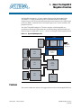

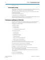
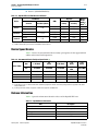

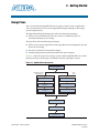

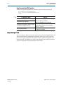
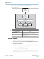
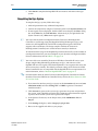

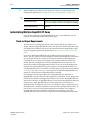
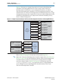


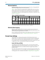
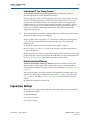
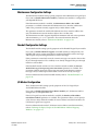
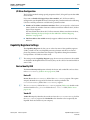


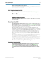


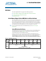
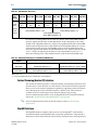
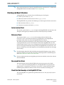
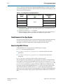
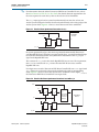
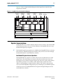
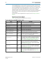

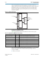


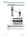
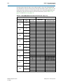
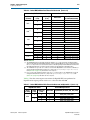
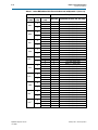
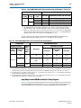
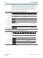
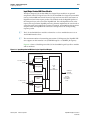


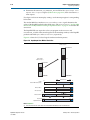
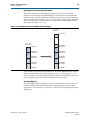
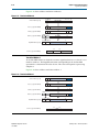
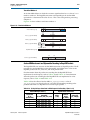
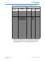
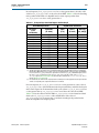
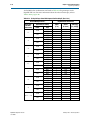
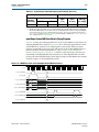
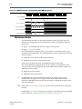
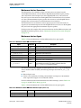
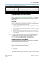


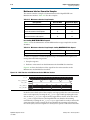
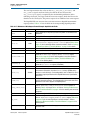
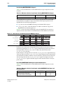
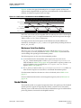

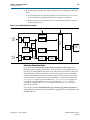
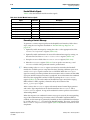

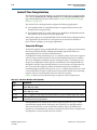
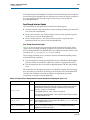
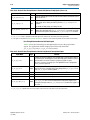
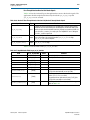
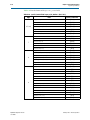
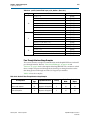
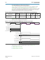
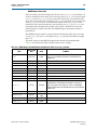
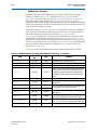
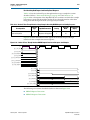
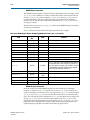


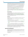


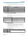
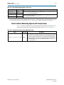
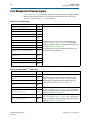
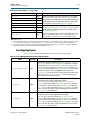

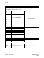
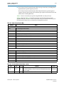
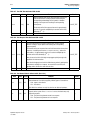
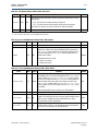
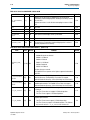
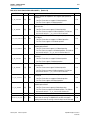
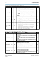
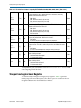
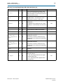
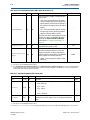
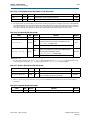
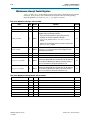
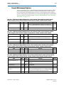
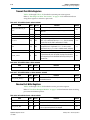
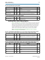
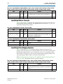
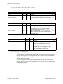
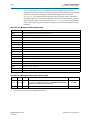
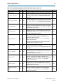
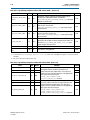
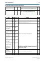
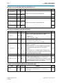

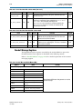
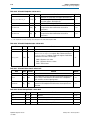


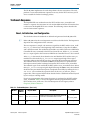
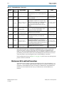

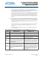


![SWITCH [ User's Guide]](http://vs1.manualzilla.com/store/data/006903573_1-63c67fc8eae32bb9b46d815d736135c6-150x150.png)