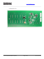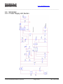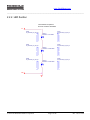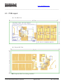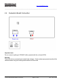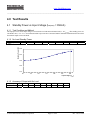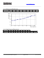
1
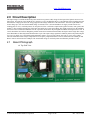
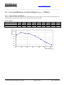
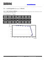
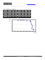
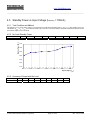
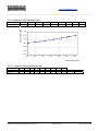
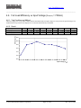
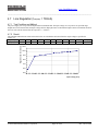
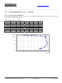
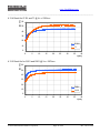
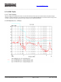
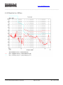
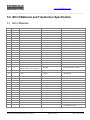
www.fairchildsemi.com
_______________________________________________________________________________________
FEB227 User’s Guide
Universal Input 12W LED Ballast
Featured Fairchild Product: FAN102MY
© 2010 Fairchild Semiconductor Corporation
Page 1 of 46
Rev 1.0, 12/2010
www.fairchildsemi.com
_______________________________________________________________________________________
Table of Contents
1.0 General Board Description
4
1.1 Contents of the Evaluation Kit
4
1.2 Power Supply Specification Table
4
2.0 Circuit Description
5
2.1 Board Photograph
5
2.2 Schematic
7
2.3 PCB Layout
9
2.4 Evaluation Board Connection
10
3.0 Test Equipment
11
4.0 Test Results
12
4.1 Standby Power vs Input Voltage (Iout(max) = 350mA)
12
4.2 Full Load Efficieny vs Input Voltage (Iout(max) = 350mA)
14
4.3 Line Regulation (Iout(max) = 350mA)
15
4.4 Load Regulation (Iout(max) = 350mA)
16
4.5 Standby Power vs Input Voltage (Iout(max) = 700mA)
18
4.6 Full Load Efficieny vs Input Voltage (Iout(max) = 700mA)
20
4.7 Line Regulation (Iout(max) = 700mA)
21
4.8 Load Regulation (Iout(max) = 700mA)
22
4.9 Output Ripple & Noise
24
4.10 Soft Start Test
26
4.11 Output Short Circuit Protection Test
28
4.12 Typical Drain Waveforms
30
4.13 Thermal Performance
34
4.14 EMI Tests
36
5.0 Bill of Materials and Transformer Specification
38
5.1 Bill of Materials
© 2010 Fairchild Semiconductor Corporation
38
Page 2 of 46
Rev 1.0, 12/2010
www.fairchildsemi.com
_______________________________________________________________________________________
5.2 Transformer Specification
39
6.0 Printed Circuit Board Special Instructions
40
7.0 Featured Products
42
7.1 FAN102 Description
42
7.1.1
FAN102 Features
42
7.1.2
FAN102 Block Diagram
43
8.0 References and Resources
44
8.1 Application Notes
44
Direct questions or comments about this Evaluation Board to:
“Worldwide Direct Support”
Fairchild Semiconductor.com
© 2010 Fairchild Semiconductor Corporation
Page 3 of 46
Rev 1.0, 12/2010
www.fairchildsemi.com
_______________________________________________________________________________________
Disclaimer
Fairchild Semiconductor Limited (“Fairchild”) provides these design services as a benefit to our
customers. Fairchild has made a good faith attempt to build for the specifications provided or needed by
the customer. Fairchild provides this product “as is” and without “recourse” and MAKES NO WARRANTY,
EXPRESSED, IMPLIED OR OTHERWISE, INCLUDING ANY WARRANTY OF MERCHANTABILITY
AND FITNESS FOR A PARTICULAR PURPOSE.
Customer agrees to do its own testing of any Fairchild design in order to ensure design meets the
customer needs. Neither Fairchild nor Customer shall be liable for incidental or consequential damages,
including but not limited to, the cost of labor, re-qualifications, rework charges, delay, lost profits, or loss of
goodwill arising out of the sale, installation or use of any Fairchild product.
Fairchild will defend any suit or proceeding brought against Customer if it is based on a claim that any of its
products infringes any U.S., Canadian, Japanese, EU or EFTA member country intellectual property right.
Fairchild must be notified promptly in writing and given full and complete authority, information and
assistance (at Fairchild’s expense) for defense of the suit. Fairchild will pay damages and costs therein
awarded against Customer but shall not be responsible for any compromise made without its consent. In
no event shall Fairchild’s liability for such damages and costs (including legal costs) exceed the
contractual value of the goods or services that are the subject of the lawsuit. In providing such defense, or
in the event that such product is held to constitute infringement and the use of the product is enjoined,
Fairchild, in its discretion, shall procure the right to continue using such product, or modify it so that it
becomes non-infringing, or remove it and grant Customer a credit for the depreciated value thereof.
Fairchild’s indemnity does not extend to claims of infringement arising from Fairchild’s compliance with
Buyer’s design, specifications and/or instructions, or use of any product in combination with other
products or in connection with a manufacturing or other process. The foregoing remedy is exclusive and
constitutes Fairchild’s sole obligation for any claim of intellectual property infringement.
All solutions, designs, schematics, drawings, boards or other information provided by Fairchild to
Customer are confidential and provided for Customer’s own use. Customer may not share any Fairchild
materials with other semiconductor suppliers. For Fairchild Semiconductor Limited
………………………………….
Name: ………………………….
Date: …………………………..
Warning
This Evaluation Board may employ high voltages so appropriate safety precautions
should be used when operating this board. Replace components on the Evaluation Board
only with those parts shown on the BOM. Contact an authorized Fairchild representative
with any questions.
© 2010 Fairchild Semiconductor Corporation
Page 4 of 46
Rev 1.0, 12/2010
www.fairchildsemi.com
_______________________________________________________________________________________
1.0 General Board Description
The FEB227 Evaluation Board is an isolated, primary-side regulated off-line AC/DC converter (power supply) in flyback
technology. It has a universal input voltage range of 85VRMS to 265VRMS at a line frequency of 50Hz to 60Hz. It has one constant
current output, selectable between 350mA and 700mA, both at a maximum output voltage of 17V. However the output current can
easily be changed by changing one resistor.
The controller used on the FEB227 Evaluation Board is Fairchild Semiconductor’s FAN102MY.
This highly integrated PWM controller provides several features to enhance the performance of low-power flyback converters. The
patented topology enables most simplified circuit design, especially for battery charger applications. The result is a low-cost,
smaller and lighter charger when compared to a conventional design or a linear transformer. The start-up current is only 10uA,
which allows use of large start-up resistance for further power saving. To minimize the standby power consumption, the proprietary
green-mode function provides off-time modulation to linearly decrease PWM frequency under light-load conditions. This
green-mode function assists the power supply to easily meet the power conservation requirement. By using FAN102, a charger can
be implemented with fewest external components and a minimized cost.
1.1
Contents of the FEB227 Evaluation Kit
1.2
Power Supply Specification Table
• FEB227 Evaluation Board
• Data sheets for the parts listed below can be obtained on the Internet from Fairchild Semiconductor's website:
http://www.fairchildsemi.com/
- FAN102MY
- DF10S
- RS1G/K
- MM3Z24VB
- ES3D
- FCD4N60
- BC846B
- Application Note: AN-6067
Minimum Line Voltage
Maximum Line Voltage
Line Frequency
Output (selectable)
© 2010 Fairchild Semiconductor Corporation
85VRMS
265VRMS
50Hz to 60Hz
350mA/700mAconstant current @ 17Vmax
Page 5 of 46
Rev 1.0, 12/2010
www.fairchildsemi.com
_______________________________________________________________________________________
2.0 Circuit Description
The input voltage is rectified and filtered by D101 and C102 to generate a DC voltage for the input of the flyback converter. Line
filter LF101, X2 capacitor C101 and the X1/Y1 capacitor C1 act as an EMI filter. R101, C106 and D102 form a clamping network
that limits the voltage spike due to the energy trapped in the leakage inductance of the transformer. After start-up R110/R112 are
used to charge up C105. Once the threshold voltage is reached, IC101 is activated and draws its supply current from the Vcc
winding (pins 4/5 of T1, rectified by D104). To keep the Vcc below a safe limit a simple linear regulator is used (C108, Q102, D105
and R111). The switching element Q101 is driven by the GATE pin via gate resistor R104. The output current level is determined by
the current sense resistors R102 and R103. If J101 is open the current flows only through R102 and thus the output current is low. If
J101 is shorted the current flows through the parallel connection of R102 and R103 and thus the output current is high. The voltage
across R102/R103 is filtered by R105 and fed into the CS pin. The output voltage regulation is indirectly achieved by monitoring the
Vcc level. To do this, Vcc is divided by R109 and R108 in order to get 2.5V at the voltage sense pin VS. C107 acts as a filter.
The FAN102SZ has a built-in slope compensation. For frequency compensation R107/C103 are connected to the COMV pin and
R106/C104 are connected to the COMI pin. The transformed voltage is rectified by D201 and filtered by the MLCC C201.
2.1
Board Photograph
• Top Side View
© 2010 Fairchild Semiconductor Corporation
Page 6 of 46
Rev 1.0, 12/2010
www.fairchildsemi.com
_______________________________________________________________________________________
•
Bottom Side View
© 2010 Fairchild Semiconductor Corporation
Page 7 of 46
Rev 1.0, 12/2010
www.fairchildsemi.com
_______________________________________________________________________________________
2.2 Schematic
2.2.1. Power Supply Unit Section
© 2010 Fairchild Semiconductor Corporation
Page 8 of 46
Rev 1.0, 12/2010
www.fairchildsemi.com
_______________________________________________________________________________________
2.2.2. LED Section
The heatsinks are optional
and have not been assembled
Iout
HS202
HS_FISCHER_FK_250_06
HS204
HS_FISCHER_FK_250_06
HS206
HS_FISCHER_FK_250_06
LED201
XREWHT-L1-000-006E5
LED202
XREWHT-L1-0000-006E5
LED203
XREWHT-L1-0000-006E5
HS201
HS_FISCHER_FK_250_06
HS203
HS_FISCHER_FK_250_06
HS205
HS_FISCHER_FK_250_06
GND
© 2010 Fairchild Semiconductor Corporation
Page 9 of 46
Rev 1.0, 12/2010
www.fairchildsemi.com
_______________________________________________________________________________________
2.3 PCB Layout
•
Top Side View
•
Bottom Side View
NB: Component D103 is not being assembled
© 2010 Fairchild Semiconductor Corporation
Page 10 of 46
Rev 1.0, 12/2010
www.fairchildsemi.com
_______________________________________________________________________________________
2.4
Evaluation Board Connection
Important note:
Do not connect anything to CONN201 while operated with the on-board LEDs!
Warning:
The circuit is line connected and contains high voltages. Caution and proper procedures should be
observed when using and making measurements on the board.
© 2010 Fairchild Semiconductor Corporation
Page 11 of 46
Rev 1.0, 12/2010
www.fairchildsemi.com
_______________________________________________________________________________________
3.0 Test Equipment
•
Oscilloscope:
•
•
•
•
•
•
TEKTRONIX TDS784C (1GHz / 4GS/s) using voltage probes P5100, P6139A and
current probe TCP202.
Analyzer:
TEKTRONIX 2712
Multimeter:
RMS MULTIMETER FLUKE 85 II
Electronic Load: Prodigit 3000C Base unit using 3311C, 3314C and 2x 3332A modules
Power Analyzer: LEM NORMA 5000
AC Source:
Chroma Programmable AC Source Model 61502
Temp. Probe:
Greisinger dual channel digital thermometer GMH3230 using two GTF300 NiCr-Ni
thermocouples
The ambient temperature for all tests was 25 ºC if not noted otherwise
© 2010 Fairchild Semiconductor Corporation
Page 12 of 46
Rev 1.0, 12/2010
www.fairchildsemi.com
_______________________________________________________________________________________
4.0 Test Results
4.1 Standby Power vs Input Voltage (Iout(max) = 350mA)
4.1.1 Test Condition and Method
The input power for various input voltages was measured at no load and at minimum load (i.e. at Vout(min)). The standby power was
calculated as PStdby = PIN – POUT. At minimum load the output current was measured and the minimum and maximum deviation from
the nominal output current calculated.
4.1.2 No Load Standby Power
85
0.30
Standby Power [W]
VIN [VRMS]
PSTDBY [W]
110
0.31
130
0.32
150
0.34
180
0.37
210
0.41
230
0.43
240
0.44
265
0.46
0.50
0.40
0.30
0.20
0.10
80
110
140
170
200
230
260
Input Voltage [V RMS ]
4.1.3 Accuracy of Output with No Load
VIN [VRMS]
Vout [V]
85
30.00
110
31.00
130
32.00
© 2010 Fairchild Semiconductor Corporation
150
32.00
180
33.00
210
34.00
230
35.00
Page 13 of 46
240
36.00
265
33.00
Rev 1.0, 12/2010
www.fairchildsemi.com
_______________________________________________________________________________________
4.1.4 Minimum Load Standby Power
85
0.41
Standby Power [W]
VIN [VRMS]
PSTDBY [W]
110
0.44
130
0.49
150
0.51
180
0.57
210
0.65
230
0.71
240
0.75
265
0.78
0.90
0.70
0.50
0.30
0.10
80
110
140
170
200
230
260
Input Voltage [V RMS ]
4.1.5 Output Current at Minimum Load
VIN [VRMS]
VOUT [V]
IOUT [mA]
85
2.8
341
110
2.8
344
130
2.8
351
150
2.8
357
© 2010 Fairchild Semiconductor Corporation
180
2.8
354
210
2.8
357
230
2.8
368
240
2.8
375
Page 14 of 46
265
2.8
342
Min [%]
-2.6
Max [%]
7.1
Rev 1.0, 12/2010
www.fairchildsemi.com
_______________________________________________________________________________________
4.2 Full Load Efficiency vs Input Voltage (Iout(max) = 350mA)
4.2.1 Test Condition and Method
The power supply was set up with its output loaded at maximum load. The input voltage was swept across the specified range. The
output load was kept constant. The input power was measured and efficiency calculated.
4.2.2 Result
85
5.20
6.63
78.38
Efficiency [%]
VIN [VRMS]
POUT [W]
PIN [W]
Efficiency [%]
110
5.24
6.64
78.95
130
5.27
6.70
78.70
150
5.30
6.73
78.68
180
5.33
6.81
78.21
210
5.36
6.91
77.51
230
5.37
6.98
76.98
240
5.38
7.01
76.79
265
5.36
7.03
76.31
79.5
79.0
78.5
78.0
77.5
77.0
76.5
76.0
80
110
140
170
200
230
260
Input Voltage [V RMS ]
© 2010 Fairchild Semiconductor Corporation
Page 15 of 46
Rev 1.0, 12/2010
www.fairchildsemi.com
_______________________________________________________________________________________
4.3 Line Regulation (Iout(max) = 350mA)
4.3.1 Test Condition and Method
The power supply was set up with its output loaded at maximum load. The input voltage was swept across its specified range.
Output current was measured for each input voltage and was displayed relative to the nominal output current. The nominal current in
this case is the current measured for the output at VIN = 230VRMS.
4.3.2 Result
Regulation [% of nominal]
The minimum and maximum values in the table below are calculated as deviations from the output voltage as specified in
section 1.2.
85
110
130
150
180
210
230
240
265 Min [%] Max [%]
VIN [VRMS]
305.40 308.20 310.00 311.30 313.10 314.90 315.90 316.50 315.20
-12.7
-9.6
IOUT [mA]
101.0
100.0
99.0
98.0
97.0
96.0
95.0
80
110
140
170
200
230
260
Input Voltage [V RMS ]
© 2010 Fairchild Semiconductor Corporation
Page 16 of 46
Rev 1.0, 12/2010
www.fairchildsemi.com
_______________________________________________________________________________________
4.4 Load Regulation (Iout(max) = 350mA)
4.4.1 Test Condition and Method
The load voltage of the output is swept from 2.0V to 19V and the output current is being measured. These measurements are done
with 110VRMS and 230VRMS input voltage.
4.4.2 Result for Vin = 110VRMS
2.00
325.00
2.25
336.00
2.50
343.00
2.80
345.60
4.38
343.80
5.96
340.00
7.53
336.00
Vout [V]
Iout [mA]
9.11
333.40
10.69
327.00
12.27
322.00
13.84
317.00
15.42
312.60
17.00
308.30
17.25
307.60
Vout [V]
Iout [mA]
17.50
305.90
17.75
271.00
18.00
230.40
18.25
183.80
18.50
142.80
18.75
105.00
19.00
70.80
Vout [V]
Vout [V]
Iout [mA]
20.0
16.0
12.0
8.0
4.0
0.0
0.0
50.0
100.0
150.0
200.0
250.0
300.0
350.0
400.0
Iout [m A]
© 2010 Fairchild Semiconductor Corporation
Page 17 of 46
Rev 1.0, 12/2010
www.fairchildsemi.com
_______________________________________________________________________________________
4.4.3 Result for Vin = 230VRMS
2.00
361.60
2.25
371.10
2.50
360.00
2.80
365.00
4.38
336.00
5.96
340.00
7.53
341.30
Vout [V]
Iout [mA]
9.11
347.00
10.69
336.80
12.27
331.00
13.84
323.00
15.42
320.60
17.00
316.00
17.25
315.10
Vout [V]
Iout [mA]
17.50
314.40
17.75
313.80
18.00
307.90
18.25
250.10
18.50
193.20
18.75
145.20
19.00
98.80
Vout [V]
Vout [V]
Iout [mA]
20.0
16.0
12.0
8.0
4.0
0.0
0.0
50.0
100.0
150.0
200.0
250.0
300.0
350.0
400.0
Iout [m A]
© 2010 Fairchild Semiconductor Corporation
Page 18 of 46
Rev 1.0, 12/2010
www.fairchildsemi.com
_______________________________________________________________________________________
4.5 Standby Power vs Input Voltage (Iout(max) = 700mA)
4.5.1 Test Condition and Method
The input power for various input voltages was measured at no load and at minimum load (i.e. at Vout(min)). The standby power was
calculated as PStdby = PIN – POUT. At minimum load the output current was measured and the minimum and maximum deviation from
the nominal output current calculated.
4.5.2 No Load Standby Power
85
0.41
Standby Power [W]
VIN [VRMS]
PSTDBY [W]
110
0.48
130
0.49
150
0.50
180
0.51
210
0.55
230
0.61
240
0.62
265
0.64
0.70
0.60
0.50
0.40
0.30
0.20
0.10
80
110
140
170
200
230
260
Input Voltage [V RMS ]
4.5.3 Accuracy of Output with No Load
VIN [VRMS]
Vout [V]
85
38.5
110
42.4
130
45.0
© 2010 Fairchild Semiconductor Corporation
150
46.0
180
46.0
210
49.0
230
49.0
Page 19 of 46
240
49.0
265
50.0
Rev 1.0, 12/2010
www.fairchildsemi.com
_______________________________________________________________________________________
4.5.4 Minimum Load Standby Power
85
0.64
Standby Power [W]
VIN [VRMS]
PSTDBY [W]
110
0.67
130
0.71
150
0.76
180
0.82
210
0.89
230
0.94
240
0.96
265
1.04
1.20
1.00
0.80
0.60
0.40
0.20
0.00
80
110
140
170
200
230
260
Input Voltage [Vrm s]
4.5.5 Output Current at Minimum Load
VIN [VRMS]
VOUT [V]
IOUT [mA]
85
2.8
536
110
2.8
555
130
2.8
566
150
2.8
576
© 2010 Fairchild Semiconductor Corporation
180
2.8
589
210
2.8
599
230
2.8
602
240
2.8
603
Page 20 of 46
265
2.8
606
Min [%]
-23.4
Max [%]
-13.4
Rev 1.0, 12/2010
www.fairchildsemi.com
_______________________________________________________________________________________
4.6 Full Load Efficiency vs Input Voltage (Iout(max) = 700mA)
4.6.1 Test Condition and Method
The power supply was set up with its output loaded at maximum load. The input voltage was swept across the specified range. The
output load was kept constant. The input power was measured and efficiency calculated.
4.6.2 Result
85
10.20
12.58
81.08
Efficiency [%]
VIN [VRMS]
POUT [W]
PIN [W]
Efficiency [%]
110
10.90
13.21
82.51
130
10.94
13.23
82.69
150
10.97
13.22
82.98
180
11.05
13.38
82.59
210
11.10
13.45
82.53
230
11.12
13.50
82.37
240
11.14
13.54
82.27
265
11.18
13.64
81.96
83.5
83.0
82.5
82.0
81.5
81.0
80.5
80
110
140
170
200
230
260
Input Voltage [V RMS ]
© 2010 Fairchild Semiconductor Corporation
Page 21 of 46
Rev 1.0, 12/2010
www.fairchildsemi.com
_______________________________________________________________________________________
4.7 Line Regulation (Iout(max) = 700mA)
4.7.1 Test Condition and Method
The power supply was set up with its output loaded at maximum load. The input voltage was swept across its specified range.
Output current was measured for each input voltage and was displayed relative to the nominal output current. The nominal current in
this case is the current measured for the output at VIN = 230VRMS.
4.7.2 Result
Regulation [% of nominal]
The minimum and maximum values in the table below are calculated as deviations from the output voltage as specified in
section 1.2.
85
110
130
150
180
210
230
240
265 Min [%] Max [%]
VIN [VRMS]
599.70 640.00 643.00 645.00 649.70 652.40 654.00 654.80 657.00
-14.3
-6.1
IOUT [mA]
102.0
100.0
98.0
96.0
94.0
92.0
90.0
80
110
140
170
200
230
260
Input Voltage [V RMS ]
© 2010 Fairchild Semiconductor Corporation
Page 22 of 46
Rev 1.0, 12/2010
www.fairchildsemi.com
_______________________________________________________________________________________
4.8 Load Regulation (Iout(max) = 700mA)
4.8.1 Test Condition and Method
The load voltage of the output is swept from 2.0V to 19V and the output current is being measured. These measurements are done
with 110VRMS and 230VRMS input voltage.
4.8.2 Result for Vin = 110VRMS
2.00
510.00
2.25
527.00
2.50
541.00
2.80
555.50
4.38
616.00
5.96
654.10
7.53
675.00
Vout [V]
Iout [mA]
9.11
677.80
10.69
670.00
12.27
663.00
13.84
655.70
15.42
648.20
17.00
640.20
17.25
638.60
Vout [V]
Iout [mA]
17.50
637.00
17.75
630.50
18.00
543.00
18.25
431.60
18.50
332.00
18.75
243.00
19.00
167.00
Vout [V]
Vout [V]
Iout [mA]
20.0
16.0
12.0
8.0
4.0
0.0
0.0
80.0
160.0
240.0
320.0
400.0
480.0
560.0
640.0
720.0
Iout [m A]
© 2010 Fairchild Semiconductor Corporation
Page 23 of 46
Rev 1.0, 12/2010
www.fairchildsemi.com
_______________________________________________________________________________________
4.8.3 Result for Vin = 230VRMS
2.00
545.00
2.25
569.00
2.50
591.00
2.80
603.00
4.38
684.50
5.96
706.00
7.53
700.00
Vout [V]
Iout [mA]
9.11
692.00
10.69
683.80
12.27
676.50
13.84
669.00
15.42
662.00
17.00
654.40
17.25
653.10
Vout [V]
Iout [mA]
17.50
651.80
17.75
648.10
18.00
625.50
18.25
585.00
18.50
442.00
18.75
322.00
19.00
217.00
Vout [V]
Vout [V]
Iout [mA]
20.0
16.0
12.0
8.0
4.0
0.0
0.0
80.0
160.0
240.0
320.0
400.0
480.0
560.0
640.0
720.0
Iout [m A]
© 2010 Fairchild Semiconductor Corporation
Page 24 of 46
Rev 1.0, 12/2010
www.fairchildsemi.com
_______________________________________________________________________________________
4.9 Output Ripple & Noise
4.9.1 Test condition and Method for Voltage Ripple and Noise
The output was loaded with the maximum load. The so-called PARD (periodic and random disturbance) method was used to
measure ripple and noise voltage in AC coupling mode. See for example Celestica application note AN-1259-1-R2.
IMPORTANT NOTE: Output voltage ripple measurements cannot be made using a normal oscilloscope probe set-up. Magnetic
field coupling into the ground connection for the oscilloscope probe could cause noise voltages far greater than the true ripple
voltage. The test was done with Iout(max) = 350mA and Iout(max) = 700mA respectively. A VIN of 110VRMS and 230VRMS was used.
4.9.2 Result for Iout(max) = 350mA
Vin = 110VRMS
Vin = 230VRMS
Ch2: VRipple @ 200mV/div,
time-base @ 5ms/div, V-Ripplep-p: 820mV
Ch2: VRipple @ 200mV/div,
time-base @ 5ms/div, V-Ripplep-p: 592mV
4.9.3 Result for Iout(max) = 700mA
Vin = 110VRMS
Vin = 230VRMS
Ch2: VRipple @ 500mV/div,
time-base @ 5ms/div, V-Ripplep-p: 1.7V
Ch2: VRipple @ 200mV/div,
time-base @ 5ms/div, V-Ripplep-p: 1.06V
© 2010 Fairchild Semiconductor Corporation
Page 25 of 46
Rev 1.0, 12/2010
www.fairchildsemi.com
_______________________________________________________________________________________
4.9.4 Test condition and Method for Current Ripple
The output was loaded with the maximum load. Using a current probe as mentioned in section 3.0. the output current was traced.
The test was done with Iout(max) = 350mA and Iout(max) = 700mA respectively. A VIN of 110VRMS and 230VRMS was used.
4.9.5 Result for Iout(max) = 350mA
Vin = 110VRMS
Vin = 230VRMS
Ch4: Iout @ 100mA/div,
time-base @ 5ms/div, I-Ripplep-p: 140mA
Ch4: Iout @ 50mA/div,
time-base @ 5ms/div, I-Ripplep-p: 101mA
4.9.6 Result for Iout(max) = 700mA
Vin = 110VRMS
Vin = 230VRMS
Ch4: Iout @ 200mA/div,
time-base @ 5ms/div, I-Ripplep-p: 308mA
Ch4: Iout @ 100mA/div,
time-base @ 5ms/div, I-Ripplep-p: 188mA
© 2010 Fairchild Semiconductor Corporation
Page 26 of 46
Rev 1.0, 12/2010
www.fairchildsemi.com
_______________________________________________________________________________________
4.10 Soft Start Test
4.10.1 Test Condition and Method
The output was loaded with the maximum load. The voltage on the output as well as the drain voltage and drain current of Q101
were measured during a power up sequence. The test was done with Iout(max) = 350mA and Iout(max) = 700mA respectively. A VIN of
110VRMS and 230VRMS was used.
4.10.2 Result for Iout(max) = 350mA @ VIN = 110VRMS
Output Voltage
Ch2: VOUT @ 5V/div, time-base @ 4ms/div
Ch1: VDrain @ 100V/div, Ch4: IDrain @ 200mA/div,
time-base @ 5ms/div, VDrain(max) = 320V
4.10.3 Result for Iout(max) = 350mA @ VIN = 230VRMS
Output Voltage
Ch2: VOUT @ 5V/div, time-base @ 4ms/div
© 2010 Fairchild Semiconductor Corporation
Drain Voltage and Drain Current
Drain Voltage and Drain Current
Ch1: VDrain @ 200V/div, Ch4: IDrain @ 200mA/div,
time-base @ 5ms/div, VDrain(max) = 504V
Page 27 of 46
Rev 1.0, 12/2010
www.fairchildsemi.com
_______________________________________________________________________________________
4.10.4 Result for Iout(max) = 700mA @ VIN = 110VRMS
Output Voltage
Ch2: VOUT @ 5V/div, time-base @ 4ms/div
Ch1: VDrain @ 100V/div, Ch4: IDrain @ 200mA/div,
time-base @ 5ms/div, VDrain(max) = 336V
4.10.5 Result for Iout(max) = 700mA @ VIN = 230VRMS
Output Voltage
Ch2: VOUT @ 5V/div, time-base @ 4ms/div
© 2010 Fairchild Semiconductor Corporation
Drain Voltage and Drain Current
Drain Voltage and Drain Current
Ch1: VDrain @ 200V/div, Ch4: IDrain @ 200mA/div,
time-base @ 5ms/div, VDrain(max) = 520V
Page 28 of 46
Rev 1.0, 12/2010
www.fairchildsemi.com
_______________________________________________________________________________________
4.11 Output Short Circuit Protection Test
4.11.1 Test Condition and Method
The output was shorted. The voltages on the Vcc, CS, COMI and COMV pins were measured with an input voltage of
VIN = 265VRMS.
4.11.2 Result for Vcc and CS pin
Ch2: Vcc @ 5V/div, Ch3: CS pin @ 100mV/div, time-base @ 100ms/div
© 2010 Fairchild Semiconductor Corporation
Page 29 of 46
Rev 1.0, 12/2010
www.fairchildsemi.com
_______________________________________________________________________________________
4.11.3 Result for COMI and COMV pin
Ch2: COMI pin @ 1V/div, Ch3: COMV pin @ 1V/div, time-base @ 40ms/div
© 2010 Fairchild Semiconductor Corporation
Page 30 of 46
Rev 1.0, 12/2010
www.fairchildsemi.com
_______________________________________________________________________________________
4.12 Typical Drain Waveforms
4.12.1 Test Condition and Method
The output was loaded with maximum load. The drain voltage and drain current of Q101 were measured. The test was done with
Iout(max) = 350mA and Iout(max) = 700mA respectively. A VIN of 110VRMS and 230VRMS was used.
4.12.2 Result for Iout(max) = 350mA @ Vin = 110VRMS
Ch1: VDrain @ 100V/div, Ch4: IDrain @ 200mA/div, time-base @ 10µs/div
© 2010 Fairchild Semiconductor Corporation
Page 31 of 46
Rev 1.0, 12/2010
www.fairchildsemi.com
_______________________________________________________________________________________
4.12.3 Result for Iout(max) = 350mA @ Vin = 230VRMS
Ch1: VDrain @ 200V/div, Ch4: IDrain @ 200mA/div, time-base @ 10µs/div
© 2010 Fairchild Semiconductor Corporation
Page 32 of 46
Rev 1.0, 12/2010
www.fairchildsemi.com
_______________________________________________________________________________________
4.12.4 Result for Iout(max) = 700mA @ Vin = 110VRMS
Ch1: VDrain @ 100V/div, Ch4: IDrain @ 200mA/div, time-base @ 10µs/div
© 2010 Fairchild Semiconductor Corporation
Page 33 of 46
Rev 1.0, 12/2010
www.fairchildsemi.com
_______________________________________________________________________________________
4.12.5 Result for Iout(max) = 700mA @ Vin = 230VRMS
Ch1: VDrain @ 200V/div, Ch4: IDrain @ 200mA/div, time-base @ 10µs/div
© 2010 Fairchild Semiconductor Corporation
Page 34 of 46
Rev 1.0, 12/2010
www.fairchildsemi.com
_______________________________________________________________________________________
4.13 Thermal Performance
4.13.1 Test Condition and Method
The temperatures of the transformer (T1), controller (IC101), MOSFET (Q101) and the secondary rectifying diode (D201) were
measured with thermocouples. The measured temperatures were monitored from start up of the PSU until a steady state was
recognized. The test was done with Iout(max) = 700mA/17V at VIN of 110VRMS and 230VRMS respectively. Tamb = 24°C.
ϑ [°C]
4.13.2 Result for IC101 and T1 @ VIN = 110VRMS
60
50
40
30
20
IC101
10
T1
0
0
5
10
15
20
25
30
35
40
t [min]
ϑ [°C]
4.13.3 Result for for Q101 and D201 @ VIN = 110VRMS
60
50
40
30
20
D201
10
Q101
0
0
5
10
15
20
25
30
35
40
t [min]
© 2010 Fairchild Semiconductor Corporation
Page 35 of 46
Rev 1.0, 12/2010
www.fairchildsemi.com
_______________________________________________________________________________________
ϑ [°C]
4.13.4 Result for IC101 and T1 @ VIN = 230VRMS
60
50
40
30
20
IC101
10
T1
0
0
5
10
15
20
25
30
35
40
t [min]
ϑ [°C]
4.13.5 Result for for Q101 and D201 @ VIN = 230VRMS
60
50
40
30
20
D201
10
Q101
0
0
5
10
15
20
25
30
35
40
t [min]
© 2010 Fairchild Semiconductor Corporation
Page 36 of 46
Rev 1.0, 12/2010
www.fairchildsemi.com
_______________________________________________________________________________________
4.14 EMI Tests
4.14.1 Test Condition
The power supply was loaded with a resistor of 26.5Ω. The GND net of the output was connected to the PE conductor. Input
voltages of 110VRMS and 230VRMS were used. The average level of the conducted EMI has been measured with the setup given in
3.0 and is compared to the Quasi-Peak and Average limits given by CISPR 22 (EN55022).
4.14.2 Result for VIN = 110VRMS
© 2010 Fairchild Semiconductor Corporation
Page 37 of 46
Rev 1.0, 12/2010
www.fairchildsemi.com
_______________________________________________________________________________________
4.14.3 Result for VIN = 230VRMS
© 2010 Fairchild Semiconductor Corporation
Page 38 of 46
Rev 1.0, 12/2010
www.fairchildsemi.com
_______________________________________________________________________________________
5.0 Bill of Materials and Transformer Specification
5.1 Bill of Materials
Item
1
2
3
4
5
6
7
8
9
10
11
12
13
14
15
16
17
18
Quantity
1
1
1
1
1
2
1
1
1
1
1
1
1
1
1
1
1
1
Reference
CONN101
CONN201
C1
C101
C102
C103, C108
C104
C105
C106
C107
C201
D101
D102
D103 (not assembled)
D104
D105
D201
FS101
HS201, HS202, HS203, HS204,
HS205, HS206 (not assembled)
IC101
19
6
20
1
21
1
J101
Jumper
22
23
24
25
26
27
28
39
30
31
32
33
34
35
3
1
1
1
1
2
1
1
1
1
1
1
2
1
LED201, LED202, LED203
LF101
Q101
Q102
R101
R102, R103
R104
R105
R106
R107
R108
R109
R110, R112
R111
XREWHT-L1-0000-006E5
2x39mH / 0.6A
FCD4N60
BC846B
100K / 2W / 5%
2R / 0.25W / 1%
10R / 0.063W / 1%
100R / 0.1W / 1%
200K / 0.1W / 1%
39K / 0.1W / 1%
7.5K / 0.1W / 1%
160K / 0.1W / 1%
750K / 0.25W / 1%
3K / 0.1W / 1%
36
1
T1
EF20/EF25 horizontal
© 2010 Fairchild Semiconductor Corporation
Part
GMKDS1,5/2
MKDSN1,5/2
2.2nF / X1Y1
220nF / X2
22uF / 400V
10nF / 50V
68nF / 16V
10uF / 25V
10nF / 500V
68pF / 16V
22uF / 25V
DF10S
RS1K
FDLL4148
RS1G
MM3Z24VB
ES3D
230V/250mA, time lag
Comment
Phoenix Contact, GMKDS 1,5
Phoenix Contact, MKDSN1,5
Murata, DE
Epcos, B32922C
Nichicon, VR
any SMD 0603
any SMD 0603
any SMD 1206
any SMD 0805
any SMD 0603
Kemet, C2220C226K3RAC
Fairchild Semiconductor
Fairchild Semiconductor
Fairchild Semiconductor
Fairchild Semiconductor
Fairchild Semiconductor
Fairchild Semiconductor
Littlefuse/Wickmann, TR5
Heatsink
Fischer Elektronik, FK250
FAN102MY
Fairchild Semiconductor
2-pin pin header, 100mil pitch plus
shorting link
Cree, XLamp XR-E
Epcos, B82731-M
Fairchild Semiconductor
Fairchild Semiconductor
Any
KOA, SR732BTTD2R00F
any SMD 0603
any SMD 0603
any SMD 0603
any SMD 0603
any SMD 0603
any SMD 0603
any SMD 1206
any SMD 0603
TDK, p/n SRW20EF-X46H014 or
see transformer spec
Page 39 of 46
Rev 1.0, 12/2010
www.fairchildsemi.com
_______________________________________________________________________________________
5.2 Transformer Specification
5.2.1
Winding Details
Name
Pins (Start →End)
W1
3→1
W2
W3
5.2.2
Strands x Wire ø
Turns
Construction
Material
2
1 x 0.20mm
100
perfect solenoid
CuLL
9,10 → 6,7
2
2 x 0.40mm
15
bifilar
triple insulated
4→5
1
1 x 0.15mm
39
spaced winding
CuLL
Electrical Characteristics
Parameter
Primary Inductance
Leakage inductance
5.2.3
Specification
2.06mH +/- 5%
42uH maximum
Conditions
100kHz, 1000mV, all secondaries open
100kHz, 1000mV, all secondaries short
E20/10/6 (EF20)
PC47, TDK or equivalent
EF20 horizontal / 10 pins with extended creepage
approx. 0.19mm for AL of 206nH/turns²
Safety
High voltage test:
5.2.5
Pins
1→3
1→3
Core and Bobbin
Core
Material
Bobbin
Gap in center leg
5.2.4
# of Layers
3000VRMS for 1 minute between primary (pins 1 to 5 ) and secondary
(pins 6 to 10)
Ordering
A complete assembled transformer following this specification can be ordered directly from TDK, partnumber:
SRW20EF-X46H014.
© 2010 Fairchild Semiconductor Corporation
Page 40 of 46
Rev 1.0, 12/2010
www.fairchildsemi.com
_______________________________________________________________________________________
6.0 Printed Circuit Board Special Instructions
Important safety precautions:
These boards are only to be operated and handled by qualified technicians and qualified engineers who have received a specific
training on the handling of high voltage laboratory boards and equipment.
DO NOT test the board without proper safety equipment, such as an isolation transformer, safety glasses and/or sun glasses.
DO NOT allow people to look directly into the LED light. LEDs are bright enough to damage your eyesight if you look directly into
the light.
DO NOT allow people to touch any part of the board, both during operation and when the board is turned off. Disconnected boards
can only be handled once they have cooled down and also someone has confirmed that all capacitors on the board have been fully
discharged. Failure to follow these rules could result in electrical shock due to high voltages or burns due to hot parts.
DO NOT test in proximity to flammable or explosive materials.
DO NOT operate the board for extended periods at Iout = 700mA, or leave it unattended while operated.
DO NOT install the board into any product.
Operation of the board:
1. Read the safety precautions above first and follow all instructions thoroughly.
2. Make sure that jumper J101 is open, i.e. the two pins are not shorted.
3. Make sure that nothing is connected to output terminal CONN201.
4. Connect an isolated variable AC source (such as a variac) to input terminal CONN101
5. Slowly increase the AC input voltage from 0VAC to at least 85VAC (Do not exceed 265VAC). Do not allow people to
look directly at the LEDs while doing so.
6. Confirm that the LEDs light up, however do not allow people to look directly at the LEDs. Caution: They already light up
at approx. Vin = 48VAC.
7. After operation remove the AC input and confirm that the circuit is de-energized.
Selecting the output current:
The board is designed to deliver a constant output current of either 350mA or 700mA respectively. This is done by opening (Iout =
350mA) or closing/shorting (Iout = 700mA) jumper J101. During operation the LEDs get hot and you must not touch them. Due to
the higher heat dissipation at Iout = 700mA it is not recommended to operate the board for an extended time in this mode. If desired,
an isolated heatsink may be applied to the backside of the board, directly beneath the LEDs.
Modification of the Board for other output currents:
The output current of the circuit is determined by a current sense resistor that is connected from source of Q101 to GND. The
relationship between the output current Io and the sense resistor RS is expressed as:
RS =
0.111875 ⋅ np
Io
np is the ratio between the number of primary and secondary windings, np =
For example, RS for an Iout of 100mA can be calculated as
N pri
. In this design np is 6.67.
N sec
0.111875 ⋅ 6.67
= 7.46 . From an E96 series pick 7.5Ω. Leave jumper
0 .1
J101 open, remove R102 and R103 and replace R102 with a 7.5Ω resistor. Higher accuracy of the calculated resistor value can be
© 2010 Fairchild Semiconductor Corporation
Page 41 of 46
Rev 1.0, 12/2010
www.fairchildsemi.com
_______________________________________________________________________________________
achieved by using two resistors in parallel. In that case replace R102 and R103 with the two resistors and close (short) jumper J101.
Please note that the whole design and especially the transformer design was laid-out for Pout(max) = 12W. Therefore the maximum
output current is 700mA. Important note: The same safety precautions as written above apply!
Modification of the Board for stand alone operation:
It is possible to test the board with your own LEDs or test the performance without the on-board LEDs.
This can be done by cutting the board. First remove all cables and connections from the board and confirm that the circuit is
de-energized. Then cut along the white line labeled ‘← Cut here for standalone operation’. After the PCB is cut into two pieces you
can use CONN201 to connect your own application to the output. Input/output specifications remain the same. Important note:
The same safety precautions as written above apply!
Connect more LEDs to the output:
Since this is a constant current output design you can drive one LED or up to six (or even more, depending on the forward voltage Vf
of the LEDs). The maximum output voltage is 17V. So, if you connect 5 LEDs, the Vf(max) of one LED should not be higher than
3.4V (2.8V for six LEDs). To connect a given number of LEDs to the output, the board must be operated stand alone, ie physically
remove the actual power supply from the on-board LEDs by cutting the board (see previous paragraph). Important note: The same
safety precautions as written above apply!
© 2010 Fairchild Semiconductor Corporation
Page 42 of 46
Rev 1.0, 12/2010
www.fairchildsemi.com
_______________________________________________________________________________________
7.0 Featured Products
7.1
FAN102 Description
The FAN102 is a highly integrated PWM controller provides several features to enhance the performance of low-power flyback
converters. The patented topology enables most simplified circuit designs, especially for battery charger applications. The result is a
low-cost, smaller and lighter charger when compared to a conventional design or a linear transformer. The start-up current is only
10uA, which allows use of large start-up resistance for further power saving. To minimize the standby power consumption, the
proprietary green-mode function provides off-time modulation to linearly decrease PWM frequency under light-load conditions.
This green-mode function assists the power supply to easily meet the power conservation requirement. By using FAN102, a charger
can be implemented with fewest external components and minimized cost.
7.1.1 FAN102 Features
•
•
•
•
•
•
•
•
•
•
•
•
•
Constant-voltage (CV) and Constant-current (CC) Control Without Secondary-feedback Circuitry
Green-mode Function: PWM Frequency Linearly Decreasing
Fixed PWM Frequency at 42kHz with Frequency Hopping to Solve EMI Problem
Cable Compensation in CV mode
Low Start-up Current 10µA
Low Operating Current 3.5mA
Peak-current-mode Control in CV mode
Cycle-by-cycle Current Limiting
VDD Over-voltage Protection with Auto-Restart
VDD Under-voltage Lockout (UVLO)
Gate Output Maximum Voltage Clamped at 18V
Fixed Over-temperature Protection with Latch
DIP-8 and SOP-8 Package Available
© 2010 Fairchild Semiconductor Corporation
Page 43 of 46
Rev 1.0, 12/2010
www.fairchildsemi.com
_______________________________________________________________________________________
7.1.2 FAN102 Block Diagram
© 2010 Fairchild Semiconductor Corporation
Page 44 of 46
Rev 1.0, 12/2010
www.fairchildsemi.com
_______________________________________________________________________________________
8.0 References and Resources
8.1 Application Notes
•
AN-6067: Design and Application of Primary-Side Regulation (PSR)
PWM Controller and EZ-Switch™
© 2010 Fairchild Semiconductor Corporation
Page 45 of 46
Rev 1.0, 12/2010
www.fairchildsemi.com
_______________________________________________________________________________________
© 2010 Fairchild Semiconductor Corporation
Page 46 of 46
Rev 1.0, 12/2010