Download Sim2 M80 Specifications

Transcript
M80 Hardware Design
M80
Quectel Cellular Engine
Hardware Design
M80_HD_V1.0
M80_HD_V1.0
-1-
M80 Hardware Design
Document Title
M80 Hardware Design
Revision
1.0
Date
2011-11-12
Status
Released
Document Control ID
M80_HD_V1.0
l
e
t
l
c
a
i
e
t
u
n
Q fide
n
o
C
General Notes
Quectel offers this information as a service to its customers, to support application and
engineering efforts that use the products designed by Quectel. The information provided is
based upon requirements specifically provided for customers of Quectel. Quectel has not
undertaken any independent search for additional information, relevant to any information
that may be in the customer’s possession. Furthermore, system validation of this product
designed by Quectel within a larger electronic system remains the responsibility of the
customer or the customer’s system integrator. All specifications supplied herein are subject to
change.
Copyright
This document contains proprietary technical information of Quectel Co., Ltd. Copying this
document, distribution to others, and communication of the contents thereof, are forbidden
without permission. Offenders are liable to the payment of damages. All rights are reserved in
the event of a patent grant or registration of a utility model or design. All specifications
supplied herein are subject to change without notice at any time.
Copyright © Shanghai Quectel Wireless Solutions Ltd. 2011
M80_HD_V1.0
-2-
M80 Hardware Design
Contents
Contents ............................................................................................................................................ 3
Table Index........................................................................................................................................ 5
Figure Index ...................................................................................................................................... 6
0. Revision history ............................................................................................................................ 8
1. Introduction ................................................................................................................................... 9
1.1. Related documents .............................................................................................................. 9
1.2. Terms and abbreviations .................................................................................................... 10
1.3. Safety caution .................................................................................................................... 12
2. Product concept ........................................................................................................................... 14
2.1. Key features ...................................................................................................................... 14
2.2. Functional diagram............................................................................................................ 16
2.3. Evaluation board ............................................................................................................... 18
3. Application interface ................................................................................................................... 19
3.1. Pin ..................................................................................................................................... 20
3.1.1. Pin assignment ......................................................................................................... 20
3.1.2. Pin description ......................................................................................................... 22
3.2. Operating modes ............................................................................................................... 31
3.3. Power supply ..................................................................................................................... 32
3.3.1. Feature of GSM power ............................................................................................ 32
3.3.2. Minimize supply voltage drop ................................................................................. 32
3.3.3. Reference power design for module ........................................................................ 33
3.3.4. Monitor power supply ............................................................................................. 34
3.4. Power on and power down scenarios ................................................................................ 34
3.4.1. Power on .................................................................................................................. 34
3.4.2. Power down ............................................................................................................. 36
3.4.3. Restart...................................................................................................................... 40
3.5. Charging interface ............................................................................................................. 41
3.6. Power saving ..................................................................................................................... 41
3.6.1. Minimum functionality mode .................................................................................. 41
3.6.2. SLEEP mode ........................................................................................................... 41
3.6.3. Wake up module from SLEEP mode ...................................................................... 42
3.7. Summary of state transitions ............................................................................................. 42
3.8. RTC backup ....................................................................................................................... 42
3.9. Serial interfaces ................................................................................................................. 44
3.9.1. UART Port .............................................................................................................. 45
3.9.2. Debug Port............................................................................................................... 49
3.9.3. Auxiliary UART Port .............................................................................................. 49
3.9.4. UART Application .................................................................................................. 50
3.10. Audio interfaces .............................................................................................................. 53
3.10.1. Decrease TDD noise and other noise .................................................................... 54
3.10.2. Microphone interfaces design................................................................................ 55
l
e
t
l
c
a
i
e
t
u
n
Q fide
n
o
C
M80_HD_V1.0
-3-
M80 Hardware Design
3.10.3. Receiver and speaker interface design................................................................... 56
3.10.4. Earphone interface design ..................................................................................... 57
3.10.5. Loud speaker interface design ............................................................................... 58
3.10.6. Audio characteristics ............................................................................................. 59
3.11. SIM card interface ........................................................................................................... 59
3.11.1. SIM card application ............................................................................................. 59
3.11.2. 6 Pin SIM cassette ................................................................................................. 61
3.11.3. 8 Pin SIM cassette ................................................................................................. 62
3.12. Camera interface ............................................................................................................. 63
3.13. SD card interface ............................................................................................................. 63
3.14. PCM interface ................................................................................................................. 63
3.15. USB interface .................................................................................................................. 63
3.16. ADC ................................................................................................................................ 64
3.17. Behaviors of the RI ......................................................................................................... 64
3.18. Network status indication ................................................................................................ 67
3.19. Operating status indication .............................................................................................. 67
4. Antenna interface ........................................................................................................................ 69
4.1. RF reference design........................................................................................................... 69
4.2. RF output power ................................................................................................................ 70
4.3. RF receiving sensitivity ..................................................................................................... 70
4.4. Operating frequencies ....................................................................................................... 70
4.5. RF cable soldering............................................................................................................. 70
5. Electrical, reliability and radio characteristics ............................................................................ 72
5.1. Absolute maximum ratings................................................................................................ 72
5.2. Operating temperature ....................................................................................................... 72
5.3. Power supply ratings ......................................................................................................... 72
5.4. Current consumption ......................................................................................................... 73
5.5. Electro-static discharge ..................................................................................................... 76
6. Mechanical dimensions ............................................................................................................... 77
6.1. Mechanical dimensions of module .................................................................................... 77
6.2. Footprint one of recommendation ..................................................................................... 79
6.3. Footprint two of recommendation ..................................................................................... 80
6.4. Top view of the module .................................................................................................... 81
6.5. Bottom view of the module ............................................................................................... 82
7. Storage and Manufacturing ......................................................................................................... 83
7.1. Storage .............................................................................................................................. 83
7.2. Soldering ........................................................................................................................... 84
7.3. Packaging .......................................................................................................................... 85
Appendix A: GPRS coding schemes............................................................................................... 86
Appendix B: GPRS multi-slot classes............................................................................................. 87
l
e
t
l
c
a
i
e
t
u
n
Q fide
n
o
C
M80_HD_V1.0
-4-
M80 Hardware Design
Table Index
TABLE 1: RELATED DOCUMENTS ..................................................................................................... 9
TABLE 2: TERMS AND ABBREVIATIONS ....................................................................................... 10
TABLE 3: MODULE KEY FEATURES ................................................................................................ 14
TABLE 4: CODING SCHEMES AND MAXIMUM NET DATA RATES OVER AIR INTERFACE .. 16
TABLE 5: M80 PIN ASSIGNMENT ..................................................................................................... 21
TABLE 6: PIN DESCRIPTION ............................................................................................................. 22
TABLE 7: OVERVIEW OF OPERATING MODES.............................................................................. 31
l
e
t
l
c
a
i
e
t
u
n
Q fide
n
o
C
TABLE 8: SUMMARY OF STATE TRANSITION ............................................................................... 42
TABLE 9: LOGIC LEVELS OF THE UART INTERFACE .................................................................. 45
TABLE 10: PIN DEFINITION OF THE UART INTERFACES ........................................................... 45
TABLE 11: PIN DEFINITION OF AUDIO INTERFACE .................................................................... 53
TABLE 12: AOUT3 OUTPUT CHARACTERISTICS .......................................................................... 54
TABLE 13: TYPICAL ELECTRET MICROPHONE CHARACTERISTICS....................................... 59
TABLE 14: TYPICAL SPEAKER CHARACTERISTICS .................................................................... 59
TABLE 15: PIN DEFINITION OF THE SIM INTERFACE ................................................................. 60
TABLE 16: PIN DESCRIPTION OF AMPHENOL SIM CARD HOLDER ......................................... 62
TABLE 17: PIN DESCRIPTION OF MOLEX SIM CARD HOLDER ................................................. 62
TABLE 18: USB INTERFACE CHARACTERISTICS ......................................................................... 63
TABLE 19: PIN DEFINITION OF THE ADC....................................................................................... 64
TABLE 20: CHARACTERISTICS OF THE ADC ................................................................................ 64
TABLE 21: BEHAVIORS OF THE RI .................................................................................................. 65
TABLE 22: WORKING STATE OF THE NETLIGHT ......................................................................... 67
TABLE 23: PIN DEFINITION OF THE STATUS ................................................................................ 67
TABLE 24: THE MODULE CONDUCTED RF OUTPUT POWER .................................................... 70
TABLE 25: THE MODULE CONDUCTED RF RECEIVING SENSITIVITY .................................... 70
TABLE 26: THE MODULE OPERATING FREQUENCIES ................................................................ 70
TABLE 27: ABSOLUTE MAXIMUM RATINGS................................................................................. 72
TABLE 28: OPERATING TEMPERATURE ......................................................................................... 72
TABLE 29: THE MODULE POWER SUPPLY RATINGS ................................................................... 72
TABLE 30: THE MODULE CURRENT CONSUMPTION.................................................................. 74
TABLE 31: THE ESD ENDURANCE (TEMPERATURE:25℃,HUMIDITY:45 %) ........................... 76
TABLE 32: DESCRIPTION OF DIFFERENT CODING SCHEMES .................................................. 86
TABLE 33: GPRS MULTI-SLOT CLASSES ........................................................................................ 87
M80_HD_V1.0
-5-
M80 Hardware Design
Figure Index
FIGURE 1: MODULE FUNCTIONAL DIAGRAM ............................................................................. 17
FIGURE 2: PIN ASSIGNMENT ............................................................................................................ 20
FIGURE 3: RIPPLE IN SUPPLY VOLTAGE DURING TRANSMITTING BURST ........................... 32
FIGURE 4: REFERENCE CIRCUIT OF THE VBAT INPUT .............................................................. 33
FIGURE 5: REFERENCE CIRCUIT OF THE SOURCE POWER SUPPLY INPUT ........................... 34
FIGURE 6: TURN ON THE MODULE USING DRIVING CIRCUIT................................................. 35
FIGURE 7: TURN ON THE MODULE USING KEYSTROKE........................................................... 35
l
e
t
l
c
a
i
e
t
u
n
Q fide
n
o
C
FIGURE 8: TIMING OF TURNING ON SYSTEM .............................................................................. 36
FIGURE 9: TIMING OF TURNING OFF THE MODULE .................................................................. 37
FIGURE 10: REFERENCE CIRCUIT FOR EMERG_OFF BY USING DRIVING CIRCUIT ............ 39
FIGURE 11: REFERENCE CIRCUIT FOR EMERG_OFF BY USING BUTTON .............................. 39
FIGURE 12: TIMING OF RESTARTING SYSTEM ............................................................................ 40
FIGURE 13: TIMING OF RESTARTING SYSTEM AFTER EMERGENCY SHUTDOWN .............. 40
FIGURE 14: RTC SUPPLY FROM NON-CHARGEABLE BATTERY ............................................... 43
FIGURE 15: RTC SUPPLY FROM RECHARGEABLE BATTERY .................................................... 43
FIGURE 16: RTC SUPPLY FROM CAPACITOR ................................................................................ 43
FIGURE 17: SEIKO XH414H-IV01E CHARGE CHARACTERISTICS ............................................. 44
FIGURE 18: CONNECTION OF ALL FUNCTIONAL UART PORT.................................................. 47
FIGURE 19: CONNECTION OF THREE LINES UART PORT .......................................................... 47
FIGURE 20: CONNECTION OF UART PORT ASSOCIATED HARDWARE FLOW CONTROL .... 48
FIGURE 21: CONNECTION OF SOFTWARE UPGRADE ................................................................. 48
FIGURE 22: CONNECTION OF SOFTWARE DEBUG ...................................................................... 49
FIGURE 23: CONNECTION OF AUXILIARY UART PORT .............................................................. 49
FIGURE 24: 3.3V LEVEL MATCH CIRCUIT...................................................................................... 50
FIGURE 25: 5V LEVEL MATCH CIRCUIT ........................................................................................ 51
FIGURE 26: RS232 LEVEL MATCH CIRCUIT .................................................................................. 52
FIGURE 27: MICROPHONE INTERFACE DESIGN OF AIN1&AIN2 .............................................. 55
FIGURE 28: RECEIVER INTERFACE DESIGN OF AOUT1 ............................................................. 56
FIGURE 29: HANDSET INTERFACE DESIGN OF AOUT2 .............................................................. 56
FIGURE 30: SPEAKER INTERFACE WITH AMPLIFIER DESIGN OF AOUT2 .............................. 57
FIGURE 31: EARPHONE INTERFACE DESIGN ............................................................................... 57
FIGURE 32: LOUD SPEAKER INTERFACE DESIGN ....................................................................... 58
FIGURE 33: REFERENCE CIRCUIT OF THE 8 PINS SIM CARD.................................................... 60
FIGURE 34: REFERENCE CIRCUIT OF THE 6 PINS SIM CARD.................................................... 61
FIGURE 35: AMPHENOL C707 10M006 512 2 SIM CARD HOLDER .............................................. 61
FIGURE 36: MOLEX 91228 SIM CARD HOLDER ............................................................................ 62
FIGURE 37: CONNECTION OF USB DOWNLOAD ......................................................................... 64
FIGURE 38: RI BEHAVIOR OF VOICE CALLING AS A RECEIVER .............................................. 65
FIGURE 39: RI BEHAVIOR OF DATA CALLING AS A RECEIVER ................................................ 66
FIGURE 40: RI BEHAVIOR AS A CALLER ........................................................................................ 66
FIGURE 41: RI BEHAVIOR OF URC OR SMS RECEIVED .............................................................. 66
M80_HD_V1.0
-6-
M80 Hardware Design
FIGURE 42: REFERENCE CIRCUIT OF THE NETLIGHT................................................................ 67
FIGURE 43: REFERENCE CIRCUIT OF THE STATUS ..................................................................... 68
FIGURE 44: REFERENCE CIRCUIT OF RF ....................................................................................... 69
FIGURE 45: RF SOLDERING SAMPLE ............................................................................................. 71
FIGURE 46: M80 TOP AND SIDE DIMENSIONS(UNIT: MM) .................................................... 77
FIGURE 47: M80 BOTTOM DIMENSIONS(UNIT: MM) ............................................................. 78
FIGURE 48: FOOTPRINT ONE OF RECOMMENDATION(UNIT: MM) .................................... 79
FIGURE 49: FOOTPRINT TWO OF RECOMMENDATION(UNIT: MM).................................... 80
FIGURE 50: TOP VIEW OF THE MODULE ....................................................................................... 81
FIGURE 51: BOTTOM VIEW OF THE MODULE .............................................................................. 82
FIGURE 52: PASTE APPLICATION .................................................................................................... 84
l
e
t
l
c
a
i
e
t
u
n
Q fide
n
o
C
FIGURE 53: RAMP-SOAK-SPIKE REFLOW PROFILE .................................................................... 85
FIGURE 54: MODULE TRAY .............................................................................................................. 85
FIGURE 55: RADIO BLOCK STRUCTURE OF CS-1, CS-2 AND CS-3 ........................................... 86
FIGURE 56: RADIO BLOCK STRUCTURE OF CS-4 ........................................................................ 86
M80_HD_V1.0
-7-
M80 Hardware Design
0. Revision history
Revision
Date
Author
Description of change
1.0
2011-11-01
Ray XU
Initial
l
e
t
l
c
a
i
e
t
u
n
Q fide
n
o
C
M80_HD_V1.0
-8-
M80 Hardware Design
1. Introduction
This document defines the M80 module and describes the hardware interface of M80 which are
connected with the customer application and the air interface.
This document can help customers quickly understand module interface specifications, electrical
and mechanical details. With the help of this document, associated application notes and user
guide, customers can use M80 module to design and set up mobile applications quickly.
l
e
t
l
c
a
i
e
t
u
n
Q fide
n
o
C
1.1. Related documents
Table 1: Related documents
SN
Document name
Remark
M80_ATC
AT command set
ITU-T
Draft
new
recommendation V.25ter
Serial asynchronous automatic dialing and control
GSM 07.07
Digital cellular telecommunications (Phase 2+); AT
command set for GSM Mobile Equipment (ME)
GSM 07.10
Support GSM 07.10 multiplexing protocol
GSM 07.05
Digital cellular telecommunications (Phase 2+); Use of
Data Terminal Equipment – Data Circuit terminating
Equipment (DTE – DCE) interface for Short Message
Service (SMS) and Cell Broadcast Service (CBS)
GSM 11.14
Digital cellular telecommunications (Phase 2+);
Specification of the SIM Application Toolkit for the
Subscriber Identity module – Mobile Equipment (SIM –
ME) interface
GSM 11.11
Digital cellular telecommunications (Phase 2+);
Specification of the Subscriber Identity module – Mobile
Equipment (SIM – ME) interface
GSM 03.38
Digital cellular telecommunications (Phase
Alphabets and language-specific information
GSM 11.10
Digital cellular telecommunications (Phase 2); Mobile
Station (MS) conformance specification; Part 1:
Conformance specification
[10]
GSM_UART_AN
UART port application notes
[11]
GSM_FW_Upgrade_AN01
GSM Firmware upgrade application note
[12]
M80_EVB_UGD
M80 EVB user guide application notes
[1]
[2]
[3]
[4]
[5]
[6]
[7]
[8]
[9]
M80_HD_V1.0
2+);
-9-
M80 Hardware Design
1.2. Terms and abbreviations
Table 2: Terms and abbreviations
Abbreviation
Description
ADC
Analog-to-Digital Converter
AMR
Adaptive Multi-Rate
ARP
Antenna Reference Point
ASIC
Application Specific Integrated Circuit
BER
Bit Error Rate
BOM
BTS
l
e
t
l
c
a
i
e
t
u
n
Q fide
n
o
C
Bill Of Material
Base Transceiver Station
CHAP
Challenge Handshake Authentication Protocol
CS
Coding Scheme
CSD
CTS
DAC
DRX
DSP
DCE
DTE
DTR
DTX
EFR
Circuit Switched Data
Clear To Send
Digital-to-Analog Converter
Discontinuous Reception
Digital Signal Processor
Data Communications Equipment (typically module)
Data Terminal Equipment (typically computer, external controller)
Data Terminal Ready
Discontinuous Transmission
Enhanced Full Rate
EGSM
Enhanced GSM
EMC
Electromagnetic Compatibility
ESD
ETS
FCC
Electrostatic Discharge
European Telecommunication Standard
Federal Communications Commission (U.S.)
FDMA
Frequency Division Multiple Access
FR
Full Rate
GMSK
Gaussian Minimum Shift Keying
GPRS
General Packet Radio Service
GSM
Global System for Mobile Communications
HR
Half Rate
I/O
Input/Output
IC
Integrated Circuit
IMEI
International Mobile Equipment Identity
Imax
Maximum Load Current
Inorm
Normal Current
kbps
Kilo Bits Per Second
LED
Light Emitting Diode
M80_HD_V1.0
- 10 -
M80 Hardware Design
Li-Ion
Lithium-Ion
Abbreviation
Description
MO
Mobile Originated
MS
Mobile Station (GSM engine)
MT
Mobile Terminated
PAP
Password Authentication Protocol
PBCCH
Packet Switched Broadcast Control Channel
PCB
Printed Circuit Board
PDU
Protocol Data Unit
PPP
Point-to-Point Protocol
RF
RMS
RTC
RX
SIM
SMS
l
e
t
l
c
a
i
e
t
u
n
Q fide
n
o
C
Radio Frequency
Root Mean Square (value)
Real Time Clock
Receive Direction
Subscriber Identification Module
Short Message Service
TDMA
Time Division Multiple Access
TE
Terminal Equipment
TX
Transmitting Direction
UART
Universal Asynchronous Receiver & Transmitter
URC
Unsolicited Result Code
USSD
Unstructured Supplementary Service Data
VSWR
Voltage Standing Wave Ratio
Vmax
Maximum Voltage Value
Vnorm
Normal Voltage Value
Vmin
Minimum Voltage Value
VIHmax
Maximum Input High Level Voltage Value
VIHmin
Minimum Input High Level Voltage Value
VILmax
Maximum Input Low Level Voltage Value
VILmin
Minimum Input Low Level Voltage Value
VImax
Absolute Maximum Input Voltage Value
VImin
Absolute Minimum Input Voltage Value
VOHmax
Maximum Output High Level Voltage Value
VOHmin
Minimum Output High Level Voltage Value
VOLmax
Maximum Output Low Level Voltage Value
VOLmin
Minimum Output Low Level Voltage Value
Phonebook abbreviations
FD
SIM Fix Dialing phonebook
LD
SIM Last Dialing phonebook (list of numbers most recently dialed)
MC
Mobile Equipment list of unanswered MT Calls (missed calls)
ON
SIM (or ME) Own Numbers (MSISDNs) list
RC
Mobile Equipment list of Received Calls
M80_HD_V1.0
- 11 -
M80 Hardware Design
SM
SIM phonebook
1.3. Safety caution
The following safety precautions must be observed during all phases of the operation, such as
usage, service or repair of any cellular terminal or mobile incorporating M80 module.
Manufacturers of the cellular terminal should send the following safety information to users and
operating personnel and to incorporate these guidelines into all manuals supplied with the product.
If not so, Quectel does not take on any liability for customer failure to comply with these
precautions.
l
e
t
l
c
a
i
e
t
u
n
Q fide
n
o
C
When in a hospital or other health care facility, observe the restrictions about the
use of mobile. Switch the cellular terminal or mobile off. Medical equipment may
be sensitive to not operate normally for RF energy interference.
Switch off the cellular terminal or mobile before boarding an aircraft. Make sure
it switched off. The operation of wireless appliances in an aircraft is forbidden to
prevent interference with communication systems. Forget to think much of these
instructions may lead to the flight safety or offend against local legal action, or
both.
Do not operate the cellular terminal or mobile in the presence of flammable gas
or fume. Switch off the cellular terminal when you are near petrol station, fuel
depot, chemical plant or where blasting operations are in progress. Operation of
any electrical equipment in potentially explosive atmosphere can constitute a
safety hazard.
Your cellular terminal or mobile receives and transmits radio frequency energy
while switched on. RF interference can occur if it is used close to TV set, radio,
computer or other electric equipment.
Road safety comes first! Do not use a hand-held cellular terminal or mobile
while driving a vehicle, unless it is securely mounted in a holder for hands-free
operation. Before making a call with a hand-held terminal or mobile, park the
vehicle.
M80_HD_V1.0
- 12 -
M80 Hardware Design
GSM cellular terminals or mobiles operate over radio frequency signal and
cellular network and cannot be guaranteed to connect in all conditions, for
example no mobile fee or an invalid SIM card. While you are in this condition
and need emergent help, Please Remember using emergency call. In order to
make or receive call, the cellular terminal or mobile must be switched on and in
a service area with adequate cellular signal strength.
Some networks do not allow for emergency call if certain network services or
phone features are in use (e.g. lock functions, fixed dialing etc.). You may have
to deactivate those features before you can make an emergency call.
l
e
t
l
c
a
i
e
t
u
n
Q fide
n
o
C
Also, some networks require that a valid SIM card be properly inserted in
cellular terminal or mobile.
M80_HD_V1.0
- 13 -
M80 Hardware Design
2. Product concept
M80 is a Quad-band GSM/GPRS engine that works at frequencies of GSM850MHz,
GSM900MHz, DCS1800MHz and PCS1900MHz. The M80 features GPRS multi-slot class 12
and supports the GPRS coding schemes CS-1, CS-2, CS-3 and CS-4. For more details about
GPRS multi-slot classes and coding schemes, please refer to Appendix A and Appendix B.
With a tiny profile of 23mm × 25mm × 2.6 mm, the module can meet almost all the requirements
for M2M applications, including Tracking and Tracing, Monitor and Security System, Wireless
POS, Intelligent Measurement, Industrial PDA, Remote Controlling, etc.
l
e
t
l
c
a
i
e
t
u
n
Q fide
n
o
C
M80 is an SMD type module with LGA package, which can be embedded in customer
applications. It provides abundant hardware interfaces between the module and customer’s host
board.
The module is designed with power saving technique so that the current consumption is as low as
1.1 mA in SLEEP mode when DRX is 5.
M80 is integrated with Internet service protocols, which are TCP/IP, UDP, FTP and PPP.
Extended AT commands have been developed for customer to use these Internet service protocols
easily.
The module fully complies to the RoHS directive of the European Union.
2.1. Key features
Table 3: Module key features
Feature
Implementation
Power supply
Single supply voltage 3.3V ~ 4.6V
Typical supply voltage 4V
Power saving
Typical power consumption in SLEEP mode: 1.1 mA@ DRX=5
0.95 mA@ DRX=9
Frequency bands




GSM class
Small MS
Transmitting power


Class 4 (2W) at GSM850 and GSM900
Class 1 (1W) at DCS1800 and PCS1900
GPRS connectivity


GPRS multi-slot class 12 (default)
GPRS multi-slot class 1~12 (configurable)
M80_HD_V1.0
Quad-band: GSM850, GSM900, DCS1800, PCS1900.
The module can search these frequency bands automatically
The frequency bands can be set by AT command.
Compliant with GSM Phase 2/2+
- 14 -
M80 Hardware Design

GPRS mobile station class B
Temperature range



Normal operation: -35°C ~ +80°C
Restricted operation: -45°C ~ -35°C and +80°C ~ +85°C 1)
Storage temperature: -45°C ~ +90°C
DATA GPRS:








GPRS data downlink transfer: max. 85.6 kbps
GPRS data uplink transfer: max. 85.6 kbps
Coding scheme: CS-1, CS-2, CS-3 and CS-4
Support the protocols PAP (Password Authentication Protocol)
usually used for PPP connections
Internet service protocols TCP/UDP/FTP/HTTP/MMS
Support Packet Switched Broadcast Control Channel (PBCCH)
CSD transmission rates: 2.4, 4.8, 9.6, 14.4 kbps non-transparent
Unstructured Supplementary Services Data (USSD) support


Text and PDU mode
SMS storage: SIM card
CSD:
SMS
FAX
l
e
t
l
c
a
i
e
t
u
n
Q fide
n
o
C
Group 3 Class 1 and Class 2
SIM interface
Support SIM card: 1.8V, 3V
Audio features
Speech codec modes:
 Half Rate (ETS 06.20)
 Full Rate (ETS 06.10)
 Enhanced Full Rate (ETS 06.50 / 06.60 / 06.80)
 Adaptive Multi-Rate (AMR)
 Echo Cancellation
 Echo Suppression
 Noise Reduction
 Embedded one amplifier of class AB with maximum driving
power up to 800mW
UART interface
UART Port:
 Seven lines on UART port interface
 Use for AT command, GPRS data and CSD data
 Multiplexing function
 Support autobauding from 4800 bps to 115200 bps
Debug Port:
 Two lines on debug UART port interface DBG_TXD and
DBG_RXD
 Debug Port only used for software debugging
Auxiliary Port:
 Use for AT command
Phonebook management
Support phonebook types: SM, ME, FD, ON, MT
SIM Application Toolkit
Support SAT class 3, GSM 11.14 Release 99
Real time clock
Implemented
Physical characteristics
Size:
23±0.15 × 25±0.15 × 2.6±0.2mm
M80_HD_V1.0
- 15 -
M80 Hardware Design
Weight: 3.3g
Firmware upgrade
Firmware upgrade via UART Port or USB Port
Antenna interface
Connected via 50 Ohm antenna pad
Table 4: Coding schemes and maximum net data rates over air interface
Coding scheme
1 Timeslot
2 Timeslot
4 Timeslot
CS-1:
9.05kbps
18.1kbps
36.2kbps
CS-2:
13.4kbps
26.8kbps
53.6kbps
CS-3:
15.6kbps
31.2kbps
62.4kbps
CS-4:
21.4kbps
42.8kbps
85.6kbps
l
e
t
l
c
a
i
e
t
u
n
Q fide
n
o
C
2.2. Functional diagram
The following figure shows a block diagram of the M80 module and illustrates the major
functional parts:





Power management
Baseband
Serial Flash
The GSM radio frequency part
The Peripheral interface
—Charging interface
—PCM interface
—SD card interface
—SIM interface
—Camera interface
—Audio interface
—UART interface
—Power supply
—RF interface
—USB interface
—ADC
—Turn on/off interface
M80_HD_V1.0
- 16 -
M80 Hardware Design
Charge
RF
PAM
Power
supply
PMU
RTC
Saw
PCM
Turn on/off
UART
Transceiver
l
e
t
l
c
a
i
e
t
u
n
Q fide
n
o
C
SIM
Baseband Engine
Camera
Audio
codec
SD
EINT
26MHz
32kHz
ADC
USB
Serial Flash
Indicator
Figure 1: Module functional diagram
M80_HD_V1.0
- 17 -
M80 Hardware Design
2.3. Evaluation board
In order to help customer to develop applications with M80, Quectel supplies an evaluation board
(EVB), RS-232 to USB cable, USB data cable, power adapter, earphone, antenna and other
peripherals to control or test the module. For details, please refer to the document [12].
l
e
t
l
c
a
i
e
t
u
n
Q fide
n
o
C
M80_HD_V1.0
- 18 -
M80 Hardware Design
3. Application interface
The module is equipped with 110 pin SMT pad and it adopts LGA package. Detailed descriptions
on Sub-interfaces included in these pads are given in the following chapters:









Power supply
Turn on/off
Power saving
RTC
UART interfaces
Audio interfaces
SIM interface
USB interface
ADC
l
e
t
l
c
a
i
e
t
u
n
Q fide
n
o
C
M80_HD_V1.0
- 19 -
M80 Hardware Design
3.1. Pin
3.1.1. Pin assignment
74 73 72 71 70 69 68 67 66 65 64 63 62 61 60 59 58 57
1
56
2
55
3
4
5
6
7
8
9
10
11
12
13
14
15
16
17
18
19
l
e
t
l
c
a
i
e
t
u
n
Q fide
n
o
C
54
94
93
92
91
53
90
52
51
75
110 109 108 107
95
106
76
96
105
77
97
78
49
88
48
87
47
86
46
104
98
103
99 100 101 102
79
50
89
45
85
44
43
80
81
82
83
42
84
41
40
39
38
20 21 22 23 24 25 26 27 28 29 30 31 32 33 34 35 36 37
VBAT
Charge
GND
RF
Camera
UART
ADC
Power
SIM
USB
Reserved
SD
Audio
PCM
Other
Figure 2: Pin assignment
M80_HD_V1.0
- 20 -
M80 Hardware Design
Table 5: M80 pin assignment
PIN NO.
PIN NAME
I/O
PIN NO.
PIN NAME
I/O
1
ADC1
I
2
ADC0
I
3
DOWNLOAD
I
4
NETLIGHT
O
5
SPK2P
O
6
AGND
7
MIC2P
I
8
MIC2N
I
9
MIC1P
I
10
MIC1N
I
11
SPK1N
O
12
SPK1P
O
13
LOUDSPKN
O
14
LOUDSPKP
O
PWRKEY
I
16
STATUS
O
EMERG_OFF
I
18
PCM_IN
I
PCM_CLK
O
20
PCM_OUT
O
PCM_SYNC
O
22
USB_DM
I/O
USB_DP
I/O
24
RESERVED
RESERVED
26
RESERVED
RESERVED
28
RESERVED
RESERVED
30
RESERVED
RESERVED
32
RESERVED
RESERVED
34
SD_CMD
O
36
SD_DATA0
I/O
GND
38
RESERVED
RESERVED
40
TXD_AUX
O
O
15
17
19
21
23
25
27
29
31
33
35
37
39
41
43
45
47
49
51
53
55
57
59
l
e
t
l
c
a
i
e
t
u
n
Q fide
n
o
C
SD_CLK
O
RXD_AUX
I
42
DBG_TXD
DBG_RXD
I
44
RESERVED
DCD
O
46
RI
O
DTR
I
48
CTS
O
TXD
O
50
RXD
I
RTS
I
52
SIM1_GND
SIM1_RST
O
54
SIM1_DATA
I/O
SIM1_CLK
O
56
SIM1_VDD
O
SIM_PRESENCE
I
58
VCAMD
O
VRTC
O
60
VDD_EXT
O
62
GND
64
GND
66
GND
61
GND
63
RF_ANT
65
GND
67
VBAT
I
68
VBAT
I
69
VBAT
I
70
BATSNS
I
71
ISENSE
I
72
CHGDET
I
M80_HD_V1.0
I/O
- 21 -
M80 Hardware Design
73
CHGLDO
75
RESERVED
77
CS_D3
79
74
GATDRV
76
RESERVED
I
78
CS_D0
I
CS_VSYNC
I
80
CS_D4
I
81
CS_D7
I
82
CS_D5
I
83
CS_PWDN
O
84
CS_D1
I
85
RESERVED
86
RESERVED
87
RESERVED
88
RESERVED
89
RESERVED
90
RESERVED
91
93
95
97
99
101
103
105
107
109
I
O
l
e
t
l
c
a
i
e
t
u
n
Q fide
n
o
C
RESERVED
92
RESERVED
GND
94
GND
SIM2_RST
O
96
CS_D2
I
CS_PCLK
I
98
CS_HSYNC
I
CS_MCLK
O
100
CS_D6
I
CS_RST
O
102
RESERVED
104
RESERVED
RESERVED
VCAMA
O
106
RESERVED
SIM2_VDD
O
108
SIM2_CLK
SIM2_DATA
I/O
110
RESERVED
O
Note: Keep all reserved pins open.
3.1.2. Pin description
Table 6: Pin description
Power supply
PIN NAME
PIN
NO.
I/O
DESCRIPTION
DC
CHARACTERISTICS
COMMENT
VBAT
67,
68,
69
I
Main power supply of
module:
VBAT=3.3V~4.6V
Vmax= 4.6V
Vmin=3.3V
Vnorm=4.0V
Make sure that supply
sufficient current in a
transmitting burst
which typically rises
to 1.6A.
59
I/O
Power supply for RTC
when VBAT is not
supplied for the
system.
Charging for backup
battery or golden
capacitor when the
VImax=VBAT
VImin=2.6V
VInorm=2.8V
VOmax=2.85V
VOmin=2.6V
VOnorm=2.8V
Iout(max)= 730uA
If unused, keep this
pin open.
VRTC
M80_HD_V1.0
- 22 -
M80 Hardware Design
VDD_EXT
60
GND
37,
61,
62,
64,
65,
66,
93,
94
O
VBAT is supplied.
Iin=2.6~5 uA
Supply 2.8V voltage
for external circuit.
Vmax=2.9V
Vmin=2.7V
Vnorm=2.8V
Imax=20mA
1. If unused, keep this
pin open.
2. Recommend to add
a 2.2~4.7uF bypass
capacitor, when using
this pin for power
supply.
Ground
l
e
t
l
c
a
i
e
t
u
n
Q fide
n
o
C
Charge interface
PIN NAME
PIN
NO.
I/O
DESCRIPTION
DC
CHARACTERISTICS
COMMENT
GATDRV
74
O
Charge passed
element control pin
CHGLDO
73
I
Charger power supply
source
CHGDET
72
I
Charger detect
ISENSE
71
I
Current sense pin
BATSNS
70
I
VBAT voltage sense
pin
PIN NAME
PIN
NO.
I/O
DESCRIPTION
DC
CHARACTERISTICS
COMMENT
PWRKEY
15
I
Power on/off key.
PWRKEY should be
pulled down for a
moment to turn on or
turn off the system.
VILmax=
0.1*VBAT
VIHmin=
0.6*VBAT
VImax=VBAT
Pulled up to VBAT
internally.
Not supported
present.
Turn on/off
Emergency shutdown
PIN NAME
PIN
NO.
I/O
DESCRIPTION
DC
CHARACTERISTICS
COMMENT
EMERG_
OFF
17
I
Emergency off. Pulled
down for at least
20ms, which will turn
off the module in case
of emergency. Use it
VILmax=0.4V
VIHmin=2.2V
Vopenmax=2.8V
Open drain/collector
driver required in
cellular device
application.
If unused, keep this
M80_HD_V1.0
- 23 -
at
M80 Hardware Design
only when normal
shutdown through
PWRKEY or AT
command can’t
perform well.
pin open.
Module indicator
PIN NAME
PIN
NO.
I/O
DESCRIPTION
DC
CHARACTERISTICS
COMMENT
STATUS
16
O
Indicate module
operating status. High
level indicates module
is power-on and low
level indicates
power-down.
VOHmin=
0.85*VDD_EXT
VOLmax=
0.15*VDD_EXT
If unused, keep this
pin open.
DC
CHARACTERISTICS
COMMENT
l
e
t
l
c
a
i
e
t
u
n
Q fide
n
o
C
Audio interface
PIN NAME
PIN
NO.
I/O
DESCRIPTION
MIC1P
MIC1N
9,10
I
Channel one of
positive and negative
voice-band input
MIC2P
MIC2N
7,8
I
Channel two of
positive and negative
voice-band input
SPK1P
SPK1N
12,11
O
Channel one of
positive and negative
voice-band output
If unused, keep these
pins open.
SPK2P
AGND
5,6
O
Channel two of
positive and negative
voice-band output
1, If unused, keep
these pins open.
2, Support both voice
and ring.
LOUDSPK
N
LOUDSPK
P
13,
14
O
Channel three of
positive and negative
voice-band output
1, If unused, keep
these pins open.
2, Embedded
amplifier of class AB
internally.
3, Support both voice
and ring.
I/O
DESCRIPTION
If unused, keep these
pins open.
Net status indicator
PIN NAME
M80_HD_V1.0
PIN
NO.
DC
CHARACTERISTICS
COMMENT
- 24 -
M80 Hardware Design
NETLIGH
T
4
O
Network status
indication
VOHmin=
0.85*VDD_EXT
VOLmax=
0.15*VDD_EXT
If unused, keep these
pins open.
Main UART port
PIN NAME
PIN
NO.
I/O
DESCRIPTION
DC
CHARACTERISTICS
COMMENT
DTR
47
I
Data terminal ready
RXD
50
I
Receiving data
TXD
49
O
Transmitting data
VILmin=-0.3V
VILmax=
0.25*VDD_EXT
VIHmin=
0.75*VDD_EXT
VIHmax=
VDD_EXT+0.3
VOHmin=
0.85*VDD_EXT
VOLmax=
0.15*VDD_EXT
If only use TXD,
RXD and GND to
communicate,
recommend keeping
other pins open.
RTS
CTS
RI
DCD
l
e
t
l
c
a
i
e
t
u
n
Q fide
n
o
C
51
I
Request to send
48
O
Clear to send
46
O
Ring indicator
45
O
Data carrier detection
Debug UART port
PIN NAME
PIN
NO.
I/O
DESCRIPTION
DC
CHARACTERISTICS
COMMENT
DBG_TXD
42
O
UART interface for
debugging only.
If unused, keep these
pins open.
DBG_RXD
43
I
VILmin=-0.3V
VILmax=
0.25*VDD_EXT
VIHmin=
0.75*VDD_EXT
VIHmax=
VDD_EXT+0.3
VOHmin=
0.85*VDD_EXT
VOLmax=
0.15*VDD_EXT
Auxiliary UART port
PIN NAME
PIN
NO.
I/O
DESCRIPTION
DC
CHARACTERISTICS
COMMENT
TXD_AUX
40
O
Transmit data
If unused, keep these
pins open.
RXD_AUX
41
I
Receive data
VILmin=-0.3V
VILmax=0.25*VDD
_EXT
VIHmin=0.75*VDD
_EXT
VIHmax=VDD_EXT
+0.3
VOHmin=0.85*VDD
_EXT
M80_HD_V1.0
- 25 -
M80 Hardware Design
VOLmax=0.15*VDD_
EXT
SIM1 interface
PIN NAME
PIN
NO.
I/O
DESCRIPTION
DC
CHARACTERISTICS
COMMENT
SIM1_
VDD
56
O
Power supply for SIM
card
The voltage can be
selected by software
automatically. Either
1.8V or 3V.
SIM1_
DATA
54
I/O
SIM data
3V:
VOLmax=0.4
VOHmin=
SIM1_VDD-0.4
1.8V:
VOLmax=
0.15*SIM1_VDD
VOHmin=
SIM1_VDD-0.4
All signals of SIM
interface should be
protected against ESD
with a TVS diode
array.
Maximum cable
length is 200mm from
the module pad to
SIM card holder.
SIM1_
CLK
l
e
t
l
c
a
i
e
t
u
n
Q fide
n
o
C
55
O
SIM clock
3V:
VOLmax=0.4
VOHmin=
0.9*SIM1_VDD
1.8V:
VOLmax=
0.12*SIM1_VDD
VOHmin=
0.9*SIM1_VDD
SIM1_RST
53
O
SIM reset
3V:
VOLmax=0.36
VOHmin=
0.9*SIM1_VDD
1.8V:
VOLmax=
0.2*SIM1_VDD
VOHmin=
0.9*SIM1_VDD
SIM1_
GND
52
SIM_PRES
ENCE
M80_HD_V1.0
57
SIM ground
I
SIM card detection
VILmin=-0.3V
VILmax=
0.25*VDD_EXT
VIHmin=
0.75*VDD_EXT
VIHmax=
If unused, keep these
pins open.
- 26 -
M80 Hardware Design
VDD_EXT+0.3
SIM2 interface
PIN NAME
PIN
NO.
I/O
DESCRIPTION
DC
CHARACTERISTICS
COMMENT
SIM2_
VDD
107
O
Power supply for SIM
card
The voltage can be
selected by software
automatically. Either
1.8V or 3V.
Not supported at
present.
SIM2_
DATA
109
I/O
SIM data
3V:
VOLmax=0.4
VOHmin=
SIM1_VDD-0.4
1.8V:
VOLmax=
0.15*SIM1_VDD
VOHmin=
SIM1_VDD-0.4
SIM2_
CLK
l
e
t
l
c
a
i
e
t
u
n
Q fide
n
o
C
108
O
SIM clock
3V:
VOLmax=0.4
VOHmin=
0.9*SIM1_VDD
1.8V:
VOLmax=
0.12*SIM1_VDD
VOHmin=
0.9*SIM1_VDD
95
O
SIM reset
3V:
VOLmax=0.36
VOHmin=
0.9*SIM1_VDD
1.8V:
VOLmax=
0.2*SIM1_VDD
VOHmin=
0.9*SIM1_VDD
PIN NAME
PIN
NO.
I/O
DESCRIPTION
DC
CHARACTERISTICS
COMMENT
ADC0
2
I
General purpose
analog to digital
converter.
Voltage range: 0V to
2.8V
If unused, keep these
pins open.
ADC1
1
I
General purpose
analog to digital
Voltage range: 0V to
2.8V
If unused, keep these
pins open.
SIM2_
RST
ADC
M80_HD_V1.0
- 27 -
M80 Hardware Design
converter.
PCM
PIN NAME
PIN
NO.
I/O
DESCRIPTION
DC
CHARACTERISTICS
COMMENT
PCM_CLK
19
O
PCM clock
PCM_IN
18
I
PCM data input
Not supported at
present.
PCM_OUT
20
O
PCM data output
PCM_
SYNC
21
O
PCM frame
synchronization
VILmin=-0.3V
VILmax=
0.25*VDD_EXT
VIHmin=
0.75*VDD_EXT
VIHmax=
VDD_EXT+0.3
VOHmin=
0.85*VDD_EXT
VOLmax=
0.15*VDD_EXT
COMMENT
l
e
t
l
c
a
i
e
t
u
n
Q fide
n
o
C
USB interface
PIN NAME
PIN
NO.
I/O
DESCRIPTION
DC
CHARACTERISTICS
USB_DM
USB_DP
22,
23
I/O
Differential data
Comply with USB 1.1
specification
PIN NAME
PIN
NO.
I/O
DESCRIPTION
DC
CHARACTERISTICS
COMMENT
SD_CMD
34
O
SD command
SD_CLK
35
O
SD clock
Not supported at
present.
SD_DATA0
36
I/O
SD data
VILmin=-0.3V
VILmax=
0.25*VDD_EXT
VIHmin=
0.75*VDD_EXT
VIHmax=
VDD_EXT+0.3
VOHmin=
0.85*VDD_EXT
VOLmax=
0.15*VDD_EXT
SD card
Camera interface
PIN NAME
PIN
NO.
I/O
DESCRIPTION
DC
CHARACTERISTICS
COMMENT
CS_D0
78
I
Camera parallel data
CS_D1
84
I
Not supported at
present.
CS_D2
96
I
CS_D3
77
I
CS_D4
80
I
CS_D5
82
I
VILmin=-0.3V
VILmax=
0.25*VDD_EXT
VIHmin=
0.75*VDD_EXT
VIHmax=
M80_HD_V1.0
- 28 -
M80 Hardware Design
CS_D6
100
I
CS_D7
81
I
CS_
VSYNC
79
I
Camera frame
synchronization
CS_
HSYNC
98
I
Camera horizontal
synchronization
CS_RST
101
O
Camera reset
CS_MCLK
97
O
Camera clock
CS_PCLK
99
I
Camera pixel clock
CS_PWDN
83
O
Camera power down
VDD_EXT+0.3
VOHmin=
0.85*VDD_EXT
VOLmax=
0.15*VDD_EXT
l
e
t
l
c
a
i
e
t
u
n
Q fide
n
o
C
VCAMD
58
O
Camera digital power
VCAMA
105
O
Camera analog power
PIN NAME
PIN
NO.
I/O
DESCRIPTION
DC
CHARACTERISTICS
RF_ANT
63
I/O
RF antenna pad
Impedance of 50Ω
RF interface
COMMENT
Other interface
PIN NAME
PIN
NO.
I/O
DESCRIPTION
DC
CHARACTERISTICS
COMMENT
DOWNLO
AD
3
I
Pull down when
download software
using USB
VILmin=-0.3V
VILmax=
0.25*VDD_EXT
VIHmin=
0.75*VDD_EXT
VIHmax=
VDD_EXT+0.3
The only function of
this pin is USB
downloading.
RESERVE
D
24,
25,
26,
27,
28,
29,
30,
31,
32,
33,
38,
39,
44,
75,
76,
85,
86,
M80_HD_V1.0
Keep these pins open.
- 29 -
M80 Hardware Design
87,
88,
89,
90,
91,
92,
102,
103,
104,
106,
110
l
e
t
l
c
a
i
e
t
u
n
Q fide
n
o
C
M80_HD_V1.0
- 30 -
M80 Hardware Design
3.2. Operating modes
The table below briefly summarizes the various operating modes in the following chapters.
Table 7: Overview of operating modes
Mode
Function
Normal operation
GSM/GPRS
SLEEP
The module will automatically go into SLEEP mode if DTR
is set to high level and there is no interrupt (such as GPIO
interrupt or data on UART port).
In this case, the current consumption of module will reduce
to the minimal level.
During SLEEP mode, the module can still receive paging
message and SMS from the system normally.
l
e
t
l
c
a
i
e
t
u
n
Q fide
n
o
C
GSM IDLE
Software is active. The module has registered to the GSM
network, and the module is ready to send and receive GSM
data.
GSM TALK
GSM connection is going. In this mode, the power
consumption is decided by the configuration of Power
Control Level (PCL), dynamic DTX control and the working
RF band.
GPRS IDLE
The module is not registered to GPRS network. The module
is not reachable through GPRS channel.
GPRS
STANDBY
The module is registered to GPRS network, but no GPRS
PDP context is active. The SGSN knows the Routing Area
where the module is located at.
GPRS
READY
The PDP context is active, but no data transfer is going on.
The module is ready to receive or send GPRS data. The
SGSN knows the cell where the module is located at.
GPRS DATA
There is GPRS data in transfer. In this mode, power
consumption is decided by the PCL, working RF band and
GPRS multi-slot configuration.
POWER DOWN
Normal shutdown by sending the “AT+QPOWD=1” command, using the
PWRKEY or the EMERG_OFF1) pin. The power management ASIC
disconnects the power supply from the base band part of the module, and only
the power supply for the RTC is remained. Software is not active. The UART
interfaces are not accessible. Operating voltage (connected to VBAT) remains
applied.
Minimum
functionality
mode (without
removing power
supply)
“AT+CFUN” command can set the module to a minimum functionality mode
without removing the power supply. In this case, the RF part of the module
will not work or the SIM card will not be accessible, or both RF part and SIM
card will be disabled all, but the UART port is still accessible. The power
consumption in this case is very low.
M80_HD_V1.0
- 31 -
M80 Hardware Design
1) Use the EMERG_OFF pin only while failing to turn off the module by the command
“AT+QPOWD=1” and the PWRKEY pin. Please refer to Section 3.4.2.2.
3.3. Power supply
3.3.1. Feature of GSM power
The unit of GSM transmit in the wireless path is pulse string which is constructed by GSMK bit
string and we call it burst. The period of burst is 4.16ms and the last time of burst is 577us. The
burst current will reach 1.6A while idle current is as low as tens of milliampere. This sudden
change of current will produce large ripple of VBAT or pull the VBAT down to 3.3V, while the
module will shut down when VBAT drops to 3.3V. Due to these features, the power design for the
module is crucial.
l
e
t
l
c
a
i
e
t
u
n
Q fide
n
o
C
The following figure is the VBAT voltage and current ripple at the maximum power transmitting
phase, the test condition is VBAT=4.0V, VBAT maximum output current =2A, C1=100µF
tantalum capacitor (ESR=0.7Ω) and C2=1µF.
4.615ms
577us
Burst:1.6A
IBAT
Max:400mV
VBAT
Figure 3: Ripple in supply voltage during transmitting burst
3.3.2. Minimize supply voltage drop
The power supply of the module is from a single voltage source of VBAT= 3.3V~4.6V. The GSM
transmitting burst can cause obvious voltage drop at the supply voltage thus the power supply
must be carefully designed and is capable of providing sufficient current up to 2A. For the VBAT
input, a bypass capacitor of about 100 µF with low ESR is recommended. Multi-layer ceramic
chip (MLCC) capacitor can provide the best combination of low ESR but small size may not be
economical. A lower cost choice could be a 100 µF tantalum capacitor with low ESR. A small
M80_HD_V1.0
- 32 -
M80 Hardware Design
(0.1µF to 1µF) ceramic capacitor should be in parallel with the 100µF capacitor, which is
illustrated in Figure 4. The capacitors should be placed close to the M80 VBAT pins.
The PCB traces from the VBAT pads to the power source must be wide enough to ensure that
there isn’t too much voltage drop occurring in the transmitting burst mode. The width of trace
should be no less than 2mm and the principle of the VBAT trace is the longer, the wider. The
VBAT voltage can be measured by oscilloscope.
VBAT
l
e
t
l
c
a
i
e
t
u
n
Q fide
n
o
C
C1
+
C2
C1=100uF, C2=0.1uF~1uF
Figure 4: Reference circuit of the VBAT input
3.3.3. Reference power design for module
The power design for the module is very important and the circuit design of the power supply for
the module largely depends on the power source. Figure 5 shows a reference design of +5V input
power source. The part number of this LDO IC is MIC29302WU. The designed output for the
power supply is 4.16V and the maximum load current is 3A, in order to prevent outputting
abnormal voltage, a zener voltage regulator is employed at the point of the output nearby the pin
of VBAT. Some elements have to be taken into account in the component select, such as Reserve
zener voltage is recommend 5.1V and the total dissipation is more than 1Watt.
M80_HD_V1.0
- 33 -
M80 Hardware Design
l
e
t
l
c
a
i
e
t
u
n
Q fide
n
o
C
Figure 5: Reference circuit of the source power supply input
3.3.4. Monitor power supply
To monitor the supply voltage, you can use the “AT+CBC” command which includes three
parameters: charging status, remaining battery capacity and voltage value (in mV). It returns the
0-100 percent of battery capacity and actual value measured between VBAT and GND. The
voltage is automatically measured in period of 5s. The displayed voltage (in mV) is averaged over
the last measuring period before the “AT+CBC” command is executed.
For details, please refer to document [1].
3.4. Power on and power down scenarios
3.4.1. Power on
The module can be turned on by PWRKEY pin.
The module is set to autobauding mode (AT+IPR=0) in default configuration. In the autobauding
mode, the URC “RDY” after powering on is not sent to host controller. When the module receives
AT command, it will be powered on after a delay of 2 or 3 seconds. Host controller should firstly
send an “AT” or “at” string in order that the module can detect baud rate of host controller, and it
should send the second or the third “AT” or “at” string until receiving “OK” string from module.
Then an “AT+IPR=x;&W” should be sent to set a fixed baud rate for module and save the
configuration to flash memory of module. After these configurations, the URC “RDY” would be
received from the UART Port of module every time when the module is powered on. Refer to
section “AT+IPR” in document [1].
The hardware flow control is disabled in default configuration. In the simple UART port which
means that only TXD, RXD, GND of the module is connected to host. CTS is pulled down
internally. In this condition, the module can transmit and receive data freely. On the other side, if
RTS, CTS connect to the host together with TXD, RXD, GND, whether or not to transmit and
M80_HD_V1.0
- 34 -
M80 Hardware Design
receive data depends on the level of RTS and CTS. Then whenever hardware flow is present or not,
the URC “RDY” is sent to host controller in the fixed band rate.
3.4.1.1. Power on module using the PWRKEY pin
Customer’s application can turn on the module by driving the pin PWRKEY to a low level voltage
and after STATUS pin outputs a high level, PWRKEY pin can be released. Customer may
monitor the level of the STATUS pin to judge whether the module is power-on or not. An open
collector driver circuit is suggested to control the PWRKEY. A simple reference circuit is
illustrated in Figure 6.
l
e
t
l
c
a
i
e
t
u
n
Q fide
n
o
C
PWRKEY
4.7K
Turn on pulse
47K
Figure 6: Turn on the module using driving circuit
The other way to control the PWRKEY is using a button directly. A TVS component is
indispensable to be placed nearby the button for ESD protection. When pressing the key,
electrostatic strike may generate from finger. A reference circuit is showed in Figure 7.
S1
PWRKEY
TVS1
Close to S1
Figure 7: Turn on the module using keystroke
The power-on scenarios is illustrated as the following figure.
M80_HD_V1.0
- 35 -
M80 Hardware Design
1
VBAT
54ms
>1s
250ms
PWRKEY
(INPUT)
VIH > 0.6*VBAT
VIL<0.1*VBAT
VDD_EXT
(OUTPUT)
l
e
t
l
c
a
i
e
t
u
n
Q fide
n
o
C
EMERG_OFF
(INPUT)
800ms
STATUS
(OUTPUT)
Figure 8: Timing of turning on system
①
Make sure that VBAT is stable before pulling down PWRKEY pin. The time between them
is recommended 30ms.
Note: Customer can monitor the voltage level of the STATUS pin to judge whether the module
is power-on. After the STATUS pin goes to high level, PWRKEY may be released. If the
STATUS pin is ignored, pull the PWRKEY pin to low level for more than 1 second to turn on
the module.
3.4.2. Power down
The following procedures can be used to turn off the module:





Normal power down procedure: Turn off module using the PWRKEY pin
Normal power down procedure: Turn off module using command “AT+QPOWD”
Over-voltage or under-voltage automatic shutdown: Take effect when over-voltage or
under-voltage is detected
Emergent power down procedure: Turn off module using the EMERG_OFF pin
Emergent power down procedure: Turn off module using command “AT+QPOWD”
M80_HD_V1.0
- 36 -
M80 Hardware Design
3.4.2.1. Power down module using the PWRKEY pin
Customer’s application can turn off the module by driving the PWRKEY to a low level voltage for
certain time. The power-down scenario is illustrated in Figure 9.
The power-down procedure causes the module to log off from the network and allows the
software to save important data before completely disconnecting the power supply, thus it is a safe
way.
Before the completion of the power-down procedure, the module sends out the result code shown
below:
NORMAL POWER DOWN
l
e
t
l
c
a
i
e
t
u
n
Q fide
n
o
C
Note: This result code does not appear when autobauding is active and DTE and DCE are not
correctly synchronized after start-up. The module is recommended to set a fixed baud rate.
After that moment, no further AT commands can be executed. Then the module enters the
POWER DOWN mode, only the RTC is still active. The POWER DOWN mode can also be
indicated by the STATUS pin, which is a low level voltage in this mode.
1s > Pulldown > 0.6s
160us
VBAT
(OUTPUT)
Logout net about 2s to 12s
PWRKEY
(INPUT)
STATUS
(OUTPUT)
VDD_EXT
(OUTPUT)
EMERG_OFF
(OUTPUT)
Figure 9: Timing of turning off the module
M80_HD_V1.0
- 37 -
M80 Hardware Design
3.4.2.2. Power down module using AT command
Customer’s application can turn off the module via AT command “AT+QPOWD=1”. This
command will let the module to log off from the network and allow the software to save important
data before completely disconnecting the power supply, thus it is a safe way.
Before the completion of the power-down procedure the module sends out the result code shown
below:
NORMAL POWER DOWN
l
e
t
l
c
a
i
e
t
u
n
Q fide
n
o
C
After that moment, no further AT commands can be executed. And then the module enters the
POWER DOWN mode, only the RTC is still active. The POWER DOWN mode can also be
indicated by STATUS pin, which is a low level voltage in this mode.
Please refer to document [1] for detail about the AT command “AT+QPOWD”.
3.4.2.3. Over-voltage or under-voltage automatic shutdown
The module will constantly monitor the voltage applied on the VBAT, if the voltage is ≤ 3.5V, the
following URC will be presented:
UNDER_VOLTAGE WARNING
If the voltage is ≥ 4.5V, the following URC will be presented:
OVER_VOLTAGE WARNING
The uncritical voltage range is 3.3V to 4.6V. If the voltage is > 4.6V or <3.3V, the module would
automatically shutdown itself.
If the voltage is <3.3V, the following URC will be presented:
UNDER_VOLTAGE POWER DOWN
If the voltage is >4.6V, the following URC will be presented:
OVER_VOLTAGE POWER DOWN
Note: These result codes don’t appear when autobauding is active and DTE and DCE are not
correctly synchronized after start-up. The module is recommended to set to a fixed baud rate.
After that moment, no further AT commands can be executed. The module logs off from network
and enters POWER DOWN mode, and only RTC is still active. The POWER DOWN mode can
also be indicated by the pin STATUS, which is a low level voltage in this mode.
M80_HD_V1.0
- 38 -
M80 Hardware Design
3.4.2.4. Emergency shutdown using EMERG_OFF pin
The module can be shut down by driving the pin EMERG_OFF to a low level voltage over 20ms
and then releasing it. The EMERG_OFF line can be driven by an Open Drain / Collector driver or a
button. The circuit is illustrated as the following figures.
EMERG_OFF
4.7K
l
e
t
l
c
a
i
e
t
u
n
Q fide
n
o
C
Emergency
shutdown pulse
47K
Figure 10: Reference circuit for EMERG_OFF by using driving circuit
S1
EMERG_OFF
TVS1
Close to S1
Figure 11: Reference circuit for EMERG_OFF by using button
3.4.2.5. Emergency shutdown using AT command
Using an AT command “AT+QPOWD=1” can achieve emergency shut down of the module. In
this situation, No URC returns back to the host no matter in the fixed band rate or auto band rate.
Be cautious to use the pin EMERG_OFF. It should only be used under emergent situation. For
instance, if the module is unresponsive or abnormal, the pin EMERG_OFF could be used to
shutdown the system. Although turning off the module by EMERG_OFF is fully tested and nothing
wrong detected, this operation is still a big risk as it could cause destroying of the code or data area
of the NOR flash memory in the module. Therefore, it is recommended that PWRKEY or AT
command should always be the preferential way to turn off the system.
M80_HD_V1.0
- 39 -
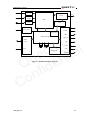
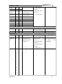
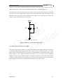
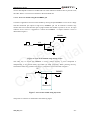
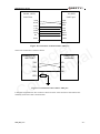
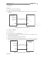
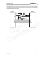
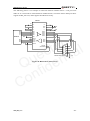
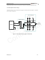
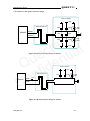
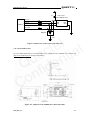
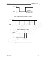
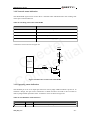
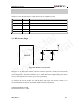
M80 Hardware Design
3.4.3. Restart
3.4.3.1. Restart module using the PWRKEY pin
Customer’s application can restart the module by driving the PWRKEY to a low level voltage for
certain time, which is similar to the way of turning on module. Before restarting the module, at
least 500ms should be delayed after detecting the low level of STATUS. The restart timing is
illustrated as the following figure.
Delay > 0.5s
l
e
t
l
c
a
i
e
t
u
n
Q fide
n
o
C
Turn off
PWRKEY
(INPUT)
Restart
H
Pull down the PWRKEY
to turn on the module
STATUS
(OUTPUT)
Figure 12: Timing of restarting system
The module can also be restarted by the PWRKEY after emergency shutdown.
6us
Pulldown > 20ms
Delay>2s
EMERG_OFF
(INPUT)
STATUS
(OUTPUT)
PWRKEY
(INPUT)
Figure 13: Timing of restarting system after emergency shutdown
3.4.3.2. Restart module using AT command
Using an AT command “AT+QPOWD=2” can achieve restart of the module. Please refer to
document [1] for detail.
M80_HD_V1.0
- 40 -
M80 Hardware Design
3.5. Charging interface
Not supported at present.
3.6. Power saving
Upon system requirement, there are several actions to drive the module to enter low current
consumption status. For example, “AT+CFUN” can be used to set module into minimum
functionality mode and DTR hardware interface signal can be used to lead system to SLEEP
mode.
l
e
t
l
c
a
i
e
t
u
n
Q fide
n
o
C
3.6.1. Minimum functionality mode
Minimum functionality mode reduces the functionality of the module to minimum level, thus
minimize the current consumption when the slow clocking mode is activated at the same time.
This mode is set with the “AT+CFUN” command which provides the choice of the functionality
levels <fun>=0,1,4.
 0: minimum functionality
 1: full functionality (default)
 4: disable both transmitting and receiving of RF part
If the module is set to minimum functionality by “AT+CFUN=0”, the RF function and SIM card
function would be disabled. In this case, the UART port is still accessible, but all AT commands
correlative with RF function or SIM card function will not be accessible.
If the module has been set by “AT+CFUN=4”, the RF function will be disabled, the UART port is
still active. In this case, all AT commands correlative with RF function will not be accessible.
After the module is set by “AT+CFUN=0” or “AT+CFUN=4”, it can return to full functionality
by “AT+CFUN=1”.
For detailed information about “AT+CFUN”, please refer to document [1].
3.6.2. SLEEP mode
The SLEEP mode is disabled in default software configuration. Customer’s application can enable
this mode by “AT+QSCLK=1”. On the other hand, the default setting is “AT+QSCLK=0” and in
this mode, the module can’t enter SLEEP mode.
When “AT+QSCLK=1” is sent to the module, customer’s application can control the module to
enter or exit from the SLEEP mode through pin DTR. When DTR is set to high level, and there is
no on-air or hardware interrupt such as GPIO interrupt or data on UART port, the module will
M80_HD_V1.0
- 41 -
M80 Hardware Design
enter SLEEP mode automatically. In this mode, the module can still receive voice, SMS or GPRS
paging from network but the UART port is not accessible.
3.6.3. Wake up module from SLEEP mode
When the module is in the SLEEP mode, the following methods can wake up the module.
 If the DTR Pin is set low, it would wake up the module from the SLEEP mode. The UART
port will be active within 20ms after DTR is changed to low level.
 Receiving a voice or data call from network wakes up module.
 Receiving an SMS from network wakes up module.
l
e
t
l
c
a
i
e
t
u
n
Q fide
n
o
C
Note: DTR pin should be held low level during communication between the module and DTE.
3.7. Summary of state transitions
Table 8: Summary of state transition
Current mode
Next mode
Power down
Power down
Normal mode
Sleep mode
Use PWRKEY
Normal mode
AT+QPOWD, use
PWRKEY pin, or use
EMERG_OFF pin
Sleep mode
Use PWRKEY pin, or
use EMERG_OFF pin
Use AT command
“AT+QSCLK=1” and pull
DTR up
Pull DTR down or
incoming call or
SMS or GPRS
3.8. RTC backup
The RTC (Real Time Clock) can be supplied by an external capacitor or battery (rechargeable or
non-chargeable) through the pin VRTC. A 1.5 K resistor has been integrated in the module for
current limiting. A coin-cell battery or a super-cap can be used to backup power supply for RTC.
The following figures show various sample circuits for RTC backup.
M80_HD_V1.0
- 42 -
M80 Hardware Design
MODULE
VRTC
1.5K
RTC
Core
Non-chargeable
Backup Battery
Figure 14: RTC supply from non-chargeable battery
l
e
t
l
c
a
i
e
t
u
n
Q fide
n
o
C
MODULE
VRTC
1.5K
RTC
Core
Rechargeable
Backup Battery
Figure 15: RTC supply from rechargeable battery
MODULE
VRTC
1.5K
Large-capacitance
Capacitor
RTC
Core
Figure 16: RTC supply from capacitor
Coin-type rechargeable capacitor such as XH414H-IV01E from Seiko can be used.
M80_HD_V1.0
- 43 -
M80 Hardware Design
l
e
t
l
c
a
i
e
t
u
n
Q fide
n
o
C
Figure 17: Seiko XH414H-IV01E Charge Characteristics
3.9. Serial interfaces
The module provides three serial ports: UART, Debug Port and Auxiliary UART Port. The
module is designed as a DCE (Data Communication Equipment), following the traditional
DCE-DTE (Data Terminal Equipment) connection. Autobauding function supports baud rate from
4800bps to 115200bps.
The UART Port:
 TXD: Send data to RXD of DTE
 RXD: Receive data from TXD of DTE
 RTS: Requests to send
 CTS: Clear to send
 DTR: DTE is ready and inform DCE (this pin can wake the module up)
 RI: Ring indicator (when the call, SMS, data of the module are coming, the module will
output signal to inform DTE)
 DCD: Data carrier detection (the valid of this pin demonstrates the communication link is set
up)
The module disables hardware flow control in default. When hardware flow control is required,
RTS and CTS should be connected to the host. AT command “AT+IFC=2,2” is used to enable
hardware flow control. AT command “AT+IFC=0,0” is used to disable the hardware flow
control. For more details, please refer to document [1].
The Debug Port
 DBG_TXD: Send data to the COM port of a debugging computer
 DBG_RXD: Receive data from the COM port of a debugging computer
M80_HD_V1.0
- 44 -
M80 Hardware Design
The Auxiliary UART Port
 TXD_AUX: Send data to the RXD of DTE
 RXD_AUX: Receive data from the TXD of DTE
The logic levels are described in the following table.
Table 9: Logic levels of the UART interface
Parameter
Min
Max
Unit
VIL
-0.3
0.25*VDD_EXT
V
VIH
0.75*VDD_EXT
VDD_EXT +0.3
V
0.15*VDD_EXT
V
VOL
VOH
l
e
t
l
c
a
i
e
t
u
n
Q fide
n
o
C
0.85*VDD_EXT
V
Table 10: Pin definition of the UART interfaces
Interface
Debug Port
UART Port
Auxiliary UART
Port
Name
Pin
Function
DBG_RXD
43
Receive data of the debug port
DBG_TXD
42
Transmit data of the debug port
RI
46
Ring indicator
RTS
51
Request to send
CTS
48
Clear to send
RXD
50
Receive data of the UART port
TXD
49
Transmit data of the UART port
DTR
47
Data terminal ready
DCD
45
Data carrier detection
RXD_AUX
41
Receive data of the Auxiliary UART
TXD_AUX
40
Transmit data of the Auxiliary UART
3.9.1. UART Port
3.9.1.1 The features of UART Port.





Seven lines on UART interface
Contain data lines TXD and RXD, hardware flow control lines RTS and CTS, other control
lines DTR, DCD and RI
Used for AT command, GPRS data, CSD FAX, etc. Multiplexing function is supported on
the UART Port. So far only the basic mode of multiplexing is available.
Support the communication baud rates as the following:
300,600,1200,2400,4800,9600,14400,19200,28800,38400,57600,115200.
The default setting is autobauding mode. Support the following baud rates for Autobauding
function:
M80_HD_V1.0
- 45 -
M80 Hardware Design
4800, 9600, 19200, 38400, 57600, 115200.
After setting a fixed baud rate or Autobauding, please send “AT” string at that rate. The UART
port is ready when it responds “OK”.
Autobauding allows the module to detect the baud rate by receiving the string “AT” or “at” from
the host or PC automatically, which gives module flexibility without considering which baud rate
is used by the host controller. Autobauding is enabled in default. To take advantage of the
autobauding mode, special attention should be paid according to the following requirements:
Synchronization between DTE and DCE:
l
e
t
l
c
a
i
e
t
u
n
Q fide
n
o
C
When DCE (the module) powers on with the autobauding enabled, it is recommended to wait 2 to
3 seconds before sending the first AT character. After receiving the “OK” response, DTE and
DCE are correctly synchronized.
If the host controller needs URC in the mode of autobauding, it must be synchronized firstly.
Otherwise the URC will be discarded.
Restrictions on autobauding operation







The UART port has to be operated at 8 data bits, no parity and 1 stop bit (factory setting).
The A/ and a/ commands can’t be used.
Only the strings “AT” or “at” can be detected (neither “At” nor “aT”).
The Unsolicited Result Codes like "RDY", "+CFUN: 1" and "+CPIN: READY” will not be
indicated when the module is turned on with autobauding enabled and not be synchronized.
Any other Unsolicited Result Codes will be sent at the previous baud rate before the module
detects the new baud rate by receiving the first “AT” or “at” string. The DTE may receive
unknown characters after switching to new baud rate.
It is not recommended to switch to autobauding from a fixed baud rate.
If autobauding is active it is not recommended to switch to multiplex mode
Note: To assure reliable communication and avoid any problems caused by undetermined baud
rate between DCE and DTE, it is strongly recommended to configure a fixed baud rate and save
it instead of using autobauding after start-up. For more details, please refer to Section
“AT+IPR” in document [1].
3.9.1.2. The connection of UART
The connection between module and host using UART port is very flexible. Three connection
styles are illustrated as below.
UART Port connection is shown as below when it is applied in modulation-demodulation.
M80_HD_V1.0
- 46 -
M80 Hardware Design
Module (DCE)
PC (DTE)
UART Port
UART port
TXD
RXD
RTS
CTS
DTR
DCD
TXD
RXD
RTS
CTS
DTR
DCD
RI
RING
l
e
t
l
c
a
i
e
t
u
n
Q fide
n
o
C
GND
GND
Figure 18: Connection of all functional UART port
Three lines connection is shown as below.
Module(DCE)
Host(DTE)
controller
UART PORT
TXD
TXD
RXD
RXD
GND
GND
RTS
0R
Figure 19: Connection of three lines UART port
UART Port with hardware flow control is shown as below. This connection will enhance the
reliability of the mass data communication.
M80_HD_V1.0
- 47 -
M80 Hardware Design
Module(DCE)
Host(DTE)
controller
UART PORT
TXD
TXD
RXD
RXD
RTS
RTS
CTS
CTS
GND
GND
l
e
t
l
c
a
i
e
t
u
n
Q fide
n
o
C
Figure 20: Connection of UART port associated hardware flow control
3.9.1.3. Software upgrade
The TXD, RXD can be used to upgrade software. The PWRKEY pin must be pulled down before
the software upgrade. Please refer to the following figures for software upgrade.
Module( DCE)
IO Connector
UART Port
TXD
TXD
RXD
RXD
GND
GND
PWRKEY
PWRKEY
Figure 21: Connection of software upgrade
M80_HD_V1.0
- 48 -
M80 Hardware Design
3.9.2. Debug Port
Debug Port
 Two lines: DBG_TXD and DBG_RXD
 It outputs log information automatically.
 Debug Port is only used for software debugging and its baud rate must be configured as
460800bps.
Module(DCE)
Debug Computer
Debug port
l
e
t
l
c
a
i
e
t
u
n
Q fide
n
o
C
DBG_TXD
TXD
DBG_RXD
RXD
GND
GND
Figure 22: Connection of software debug
3.9.3. Auxiliary UART Port
Auxiliary UART Port
 Two data lines: TXD_AUX and RXD_AUX
 Auxiliary UART port is used for AT command only and doesn’t support GPRS data, CSD
FAX, Multiplexing function etc.
 Support the communication baud rates as the following:
4800, 9600, 14400, 19200,28800,38400,57600,115200.
 The default baud rate setting is 115200bps, and doesn’t support autobauding. The baud rate
can be modified by AT+QSEDCB command. For more details, please refer to document [1].
Module(DCE)
Host(DTE)
controller
TXD_AUX
TXD
RXD_AUX
RXD
GND
GND
Figure 23: Connection of Auxiliary UART port
M80_HD_V1.0
- 49 -
M80 Hardware Design
3.9.4. UART Application
The reference design of 3.3V level match is shown as below. 1K resistors among the following
diagram are used to decrease the output voltage of MCU/ARM.
MODULE
MCU/ARM
VBAT
GND
/TXD
1K
RXD
TXD
l
e
t
l
c
a
i
e
t
u
n
Q fide
n
o
C
/RXD
/RTS
/CTS
GPIO
1K
1K
RTS
CTS
DTR
EINT
RI
GPIO
STATUS
voltage level: 3.3V
Figure 24: 3.3V level match circuit
Note: The above reference design is also suitable for 3V system.
M80_HD_V1.0
- 50 -
M80 Hardware Design
The reference design of 5V level match is shown as below. The construction of dotted line can
refer to the construction of solid line. Please pay attention to direction of connection. Input dotted
line of module should refer to input solid line of the module. Output dotted line of module should
refer to output solid line of the module.
MCU/ARM
MODULE
VDD_EXT
4.7k
VBAT
GND
4.7k
VCC_MCU
1K
/TXD
RXD
TXD
/RXD
l
e
t
l
c
a
i
e
t
u
n
Q fide
n
o
C
4.7k
4.7k
VCC_MCU
VDD_EXT
/RTS
/CTS
GPIO
EINT
GPIO
RTS
CTS
DTR
RI
STATUS
voltage level: 5V
Figure 25: 5V level match circuit
M80_HD_V1.0
- 51 -
M80 Hardware Design
The following picture is an example of connection between module and PC. A RS_232 level
shifter IC or circuit must be inserted between module and PC, since these three UART ports don’t
support the RS_232 level, while support the CMOS level only.
SP3238
28
25
1
3
DCD
TXD
CTS
RI
C1+
V+
C1-
GND
C2+
VCC
C2-
V-
24
23
22
19
T1IN
T2IN
T3IN
T4IN
17
T5IN
T4OUT
T2OUT
T3OUT
T1OUT
T5OUT
27
2
26
4
GND
3V
GND
10
6
7
5
12
l
e
t
l
c
a
i
e
t
u
n
Q fide
n
o
C
MODULE
GND
16
21
20
18
RXD
DTR
RTS
3V
13
/R1OUT
R1OUT
R2OUT
R3OUT
R1IN
R2IN
R3IN
8
9
11
ONLINE
15
/STATUS
14
/SHUTDOWN
6
7
8
9
TO PC serial port
1
2
3
4
5
GND
Figure 26: RS232 level match circuit
M80_HD_V1.0
- 52 -
M80 Hardware Design
3.10. Audio interfaces
The module provides two analogy input channels and three analogy output channels.
Table 11: Pin definition of Audio interface
Interface
AIN1/AOUT1
Name
Pin
Function
MIC1P
9
Channel one of Microphone positive input
MIC1N
10
Channel one of Microphone negative input
SPK1P
12
Channel one of Audio positive output
SPK1N
11
Channel one of Audio negative output
MIC2P
7
Channel two of Microphone positive input
MIC2N
8
Channel two of Microphone negative input
SPK2P
5
Channel two of Audio positive output
AGND
6
Cooperate with SPK2P
LOUDSPKP
14
Channel three of Audio positive output
LOUDSPKN
13
Channel three of Audio negative output
l
e
t
l
c
a
i
e
t
u
n
Q fide
n
o
C
AIN2/AOUT2
AIN2/AOUT3
AIN1 and AIN2 can be used for input of microphone and line. An electret microphone is usually
used. AIN1 and AIN2 are both differential input channels.
AOUT1 is used for output of the receiver and speaker. This channel is typically used for a receiver
built into a handset. AOUT1 channel is a differential channel. It only supports voice path. If it is
used as a speaker, an amplifier should be employed.
AOUT2 is used for output of earphone and speaker. This channel is typically used with earphone.
AOUT2 is a single-ended channel. SPK2P and AGND can establish a pseudo differential mode. If
customer needs to play Melody or Midi ring tone for incoming call, AOUT2 Channel should
always be used. If it is used as a speaker, an amplifier should be employed also.
AOUT3 is used for loud speaker output as it embedded an amplifier of class AB whose maximum
drive power is 800mW. AOUT3 is a differential channel. Immediately Playing Melody or Midi
ring tone for incoming call is available in AOUT3.
These three audio channels can be swapped by “AT+QAUDCH” command. For more details,
please refer to document [1].
Use AT command “AT+QAUDCH” to select audio channel:
 0--AIN1/AOUT1, the default value is 0.
 1--AIN2/AOUT2
 2--AIN2/AOUT3
M80_HD_V1.0
- 53 -
M80 Hardware Design
For each channel, customer can use AT+QMIC to adjust the input gain level of microphone.
Customer can also use “AT+CLVL” to adjust the output gain level of receiver and speaker.
“AT+QECHO” is used to set the parameters for echo cancellation control. “AT+QSIDET” is used
to set the side-tone gain level. For more details, please refer to document [1].
Table 12: AOUT3 output characteristics
Item
Condition
min
type
max
unit
RMS power
8ohm load
VBAT=4.3v
THD+N=1%
800
8ohm load
VBAT=3.7v
THD+N=1%
700
mW
8ohm load
VBAT=3.2v
THD+N=1%
500
mW
mW
l
e
t
l
c
a
i
e
t
u
n
Q fide
n
o
C
Gain adjustment range
Gain adjustment steps
0
18
3
dB
dB
3.10.1. Decrease TDD noise and other noise
The 33pF capacitor is applied for filtering out 900MHz RF interference when the module is
transmitting at GSM900MHz. Without placing this capacitor, TDD noise could be heard.
Moreover, the 10pF capacitor here is for filtering out 1800MHz RF interference. However, the
resonant frequency point of a capacitor largely depends on the material and production technique.
Therefore, customer would have to discuss with its capacitor vendor to choose the most suitable
capacitor for filtering out GSM850MHz, GSM900MHz, DCS1800MHz and PCS1900MHz
separately.
The severity degree of the RF interference in the voice channel during GSM transmitting period
largely depends on the application design. In some cases, GSM900 TDD noise is more severe;
while in other cases, DCS1800 TDD noise is more obvious. Therefore, customer can have a
choice based on test results. Sometimes, even no RF filtering capacitor is required.
The capacitor which is used for filtering out RF noise should be close to RJ11 or other audio
interfaces. Audio alignment should be as short as possible.
In order to decrease radio or other signal interference, the position of RF antenna should be kept
away from audio interface and audio alignment. Power alignment and audio alignment should not
be parallel, and power alignment should be far away from audio alignment.
M80_HD_V1.0
- 54 -
M80 Hardware Design
The differential audio traces have to be placed according to the differential signal layout rule.
3.10.2. Microphone interfaces design
AIN1/IN2 channels come with internal bias supply for external electret microphone. A reference
circuit is shown in Figure 27.
Close to Microphone
l
e
t
l
c
a
i
e
t
u
n
Q fide
n
o
C
GND
GND
GND
Differential layout
10pF
33pF
10pF
33pF
ESD
ANTI
MICxP
Module
Electret
Microphone
MICxN
AGND
GND
ESD
ANTI
33pF
10pF
GND
GND
Figure 27: Microphone interface design of AIN1&AIN2
M80_HD_V1.0
- 55 -
M80 Hardware Design
3.10.3. Receiver and speaker interface design
Close to speaker
GND
Differential layout
Module
10pF
33pF
10pF
33pF
10pF
33pF
ESD
ANTI
SPK1P
l
e
t
l
c
a
i
e
t
u
n
Q fide
n
o
C
SPK1N
ESD
ANTI
GND
Figure 28: Receiver interface design of AOUT1
Close to speaker
GND
Differential layout
10pF
Module
SPK2P
22uF
33pF
ESD
ANTI
AGND
Figure 29: Handset interface design of AOUT2
M80_HD_V1.0
- 56 -
M80 Hardware Design
Close to speaker
GND
Differential layout
Module
SPK2P
Amplifier
circuit
10pF
33pF
ESD
ANTI
10pF
33pF
ESD
ANTI
C1
AGND
C2
l
e
t
l
c
a
i
e
t
u
n
Q fide
n
o
C
GND
Figure 30: Speaker interface with amplifier design of AOUT2
Texas Instrument’s TPA6205A1is recommended for a suitable differential audio amplifier. There
are plenty of excellent audio amplifiers in the market.
Note: The value of C1 and C2 depends on the input impedance of audio amplifier.
3.10.4. Earphone interface design
Close to Socket
Differential layout
GND
4.7uF
33pF
MIC2N
MIC2P
GND
GND
33pF
68R
Module
22uF
SPK2P
AGND
3
33pF
4
2
1
10pF
Amphenol
9001-8905-050
AGND
GND
AGND
GND
GND
Figure 31: Earphone interface design
M80_HD_V1.0
- 57 -
M80 Hardware Design
3.10.5. Loud speaker interface design
Close to speaker
GND
Differential layout
10pF
33pF
ESD ANTI
0R
Module
LOUDSPKP
100pF
0R
LOUDSPKN
l
e
t
l
c
a
i
e
t
u
n
Q fide
n
o
C
10pF
33pF
ESD
ANTI
GND
Figure 32: Loud speaker interface design
M80_HD_V1.0
- 58 -
M80 Hardware Design
3.10.6. Audio characteristics
Table 13: Typical electret microphone characteristics
Parameter
Min
Typ
Max
Unit
Working Voltage
1.2
1.5
2.0
V
Working Current
200
500
uA
External
Microphone
Load Resistance
2.2
k Ohm
l
e
t
l
c
a
i
e
t
u
n
Q fide
n
o
C
Table 14: Typical speaker characteristics
Parameter
Normal Output
(AOUT1)
Single
Ended
Differential
Auxiliary
Output
(AOUT2)
Output
(AOUT3)
Single
Ended
Differential
Min
Typ
Load
Resistance
28
32
Ref level
0
Load
Resistance
28
Ref level
0
Load
Resistance
16
Ref level
0
Load
Resistance
Ref level
Max
Ohm
2.4
32
Vpp
Ohm
4.8
32
Vpp
Load
Resistance
2.4
8
0
Unit
Vpp
Load
Resistance
2*VBAT
Vpp
3.11. SIM card interface
3.11.1. SIM card application
The SIM interface supports the functionality of the GSM Phase 1 specification and also supports
the functionality of the new GSM Phase 2+ specification for FAST 64 kbps SIM card, which is
intended for use with a SIM application Tool-kit.
The SIM interface is powered from an internal regulator in the module. Both 1.8V and 3.0V SIM
Cards are supported.
M80_HD_V1.0
- 59 -
M80 Hardware Design
Table 15: Pin definition of the SIM interface
Name
Pin
Function
SIM1_VDD
56
Supply power for SIM Card. Automatic detection of
SIM card voltage. 3.0V±10% and 1.8V±10%. Maximum
supply current is around 10mA.
SIM1_DATA
54
SIM Card data I/O
SIM1_CLK
55
SIM Card clock
SIM1_RST
53
SIM Card reset
SIM_PRESENCE
57
SIM Card detect
l
e
t
l
c
a
i
e
t
u
n
Q fide
n
o
C
SIM1_GND
52
SIM Card ground
Figure 33 is the reference circuit for SIM interface, and here an 8-pin SIM card holder is used. In
order to offer good ESD protection, it is recommended to add TVS such as WILL
(http://www.willsemi.com) ESDA6V8AV6. The 22Ω resistors should be added in series between
the module and the SIM card so as to suppress the EMI spurious transmission and enhance the
ESD protection. Note that the SIM peripheral circuit should be close to the SIM card socket.
To avoid possible cross-talk from the SIM_CLK signal to the SIM_DATA signal, be careful that
both lines should be not close to each other. A useful approach is to use GND line to shield the
SIM_DATA line from the SIM_CLK line.
VDD_EXT
100K
MODULE
1uF
SIM1_VDD
SIM1_RST
22R
SIM1_CLK
22R
VCC
GND
RST
VPP
CLK
I/O
PRESENCE GND
SIM_PRESENCE
SIM1_DATA
SIM CARD
MOLEX-91228
22R
SIM1_GND
SMF05C
GND
Figure 33: Reference circuit of the 8 pins SIM card
If customer doesn’t need the SIM card detection function, keep SIM_PRESENCE open. The
reference circuit using a 6-pin SIM card socket is illustrated as the following figure.
M80_HD_V1.0
- 60 -
M80 Hardware Design
1uF
SIM CARD
C707 10M006 512 2
SIM1_VDD
SIM1_RST
Module
VCC
RST
CLK
22R
SIM1_CLK
22R
SIM1_DATA
GND
VPP
I/O
22R
SMF05C
l
e
t
l
c
a
i
e
t
u
n
Q fide
n
o
C
GND
Figure 34: Reference circuit of the 6 pins SIM card
3.11.2. 6 Pin SIM cassette
For 6-pin SIM card holder, it is recommended to use Amphenol C707 10M006 512 2. Please visit
http://www.amphenol.com for more information.
Figure 35: Amphenol C707 10M006 512 2 SIM card holder
M80_HD_V1.0
- 61 -
M80 Hardware Design
Table 16: Pin description of Amphenol SIM card holder
Name
Pin
Function
SIM_VDD
C1
SIM Card Power Supply
SIM_RST
C2
SIM Card Reset
SIM_CLK
C3
SIM Card Clock
GND
C5
Ground
VPP
C6
Not Connect
SIM_DATA
C7
SIM Card data I/O
l
e
t
l
c
a
i
e
t
u
n
Q fide
n
o
C
3.11.3. 8 Pin SIM cassette
For 8-pin SIM card holder, it is recommended to use Molex 91228. Please visit
http://www.molex.com for more information.
Figure 36: Molex 91228 SIM card holder
Table 17: Pin description of Molex SIM card holder
Name
Pin
Function
SIM_VDD
C1
SIM Card Power supply
SIM_RST
C2
SIM Card Reset
M80_HD_V1.0
- 62 -
M80 Hardware Design
SIM_CLK
C3
SIM Card Clock
SIM_PRESENCE
C4
SIM Card Presence Detection
GND
C5
Ground
VPP
C6
Not Connect
SIM_DATA
C7
SIM Card Data I/O
SIM_DETECT
C8
Pulled down GND with external circuit. When the tray is
present, C4 is connected to C8.
3.12. Camera interface
l
e
t
l
c
a
i
e
t
u
n
Q fide
n
o
C
Not supported at present.
3.13. SD card interface
Not supported at present.
3.14. PCM interface
Not supported at present.
3.15. USB interface
M80 provides USB interface which complies with USB 1.1 FS/LS specification. It supports
12Mbps in full speed mode. It cannot act as a host device.
Table 18: USB interface characteristics
Name
Pin
Function
USB_DM
22
USB data negative
USB_DP
23
USB data positive
USB interface only supports downloading software and should cooperate with DOWNLOAD pin.
M80_HD_V1.0
- 63 -
M80 Hardware Design
Module (DCE)
IO Connector
USB_DM
USB_DM
USB_DP
USB_DP
GND
GND
DOWNLOAD
PWRKEY
l
e
t
l
c
a
i
e
t
u
n
Q fide
n
o
C
Figure 37: Connection of USB download
3.16. ADC
The module provides two ADC to measure the value of voltage. Use AT command “AT+QADC”
to read the voltage value on ADC1 pin. Use AT command “AT+QEADC” to read the voltage
value on ADC0 pin. For details of this AT command, please refer to document [1]. In order to
improve the accuracy of ADC, the alignment of ADC should be surrounded by ground.
Table 19: Pin definition of the ADC
Name
ADC0
ADC1
Pin
Function
2
Analog to digital converter.
1
Analog to digital converter.
Table 20: Characteristics of the ADC
Item
Voltage Range
Min
Typ
0
Max
Units
2.8
V
ADC Resolution
10
bits
ADC Accuracy
2.7
mV
3.17. Behaviors of the RI
M80_HD_V1.0
- 64 -
M80 Hardware Design
Table 21: Behaviors of the RI
State
RI respond
Standby
HIGH
Voice calling
Change to LOW, then:
(1) Change to HIGH when call is established.
(2) Use ATH to hang up the call, change to HIGH.
(3) Calling part hangs up, change to HIGH first, and change to LOW for
120ms indicating “NO CARRIER” as an URC, then change to HIGH
again.
(4) Change to HIGH when SMS is received.
l
e
t
l
c
a
i
e
t
u
n
Q fide
n
o
C
Data calling
Change to LOW, then:
(1) Change to HIGH when data connection is established.
(2) Use ATH to hang up the data calling, change to HIGH.
(3) Calling part hangs up, change to HIGH first, and change to LOW for
120ms indicating “NO CARRIER” as an URC, then change to HIGH
again.
(4) Change to HIGH when SMS is received.
SMS
When a new SMS comes, the RI changes to LOW and holds low level for
about 120 ms, then changes to HIGH.
URC
Certain URCs can trigger 120ms low level on RI. For more details, please
refer to the document [10].
If the module is used as a caller, the RI would maintain high except the URC or SMS is received.
On the other hand, when it is used as a receiver, the timing of the RI is shown below.
HIGH
RI
LOW
Idle
Ring
Off-hook by
“ATA”. On-hook
by “ATH”. SMS
received.
Figure 38: RI behavior of voice calling as a receiver
M80_HD_V1.0
- 65 -
M80 Hardware Design
HIGH
RI
Data calling
establish. On-hook
by “ATH”. SMS
received
LOW
Idle
Ring
Figure 39: RI behavior of data calling as a receiver
l
e
t
l
c
a
i
e
t
u
n
Q fide
n
o
C
HIGH
RI
LOW
Idle
Calling
Talking
On-hook
Idle
Figure 40: RI behavior as a caller
HIGH
RI
120ms
LOW
Idle or
talking
URC or
SMS Received
Figure 41: RI behavior of URC or SMS received
M80_HD_V1.0
- 66 -
M80 Hardware Design
3.18. Network status indication
The NETLIGHT signal can be used to drive a network status indication LED. The working state
of this pin is listed in Table 22.
Table 22: Working state of the NETLIGHT
State
Module function
Off
The module is not running.
64ms On/ 800ms Off
The module is not synchronized with network.
l
e
t
l
c
a
i
e
t
u
n
Q fide
n
o
C
64ms On/ 2000ms Off
The module is synchronized with network.
64ms On/ 600ms Off
GPRS data transfer is ongoing.
A reference circuit is shown in Figure 42.
VBAT
300R
Module
4.7K
NETLIGHT
47K
Figure 42: Reference circuit of the NETLIGHT
3.19. Operating status indication
The STATUS pin is set as an output pin and can be used to judge whether module is power-on. In
customer’s design, this pin can be connected to a GPIO of DTE or be used to drive an LED in
order to judge module operation status. A reference circuit is shown in Figure 43.
Table 23: Pin definition of the STATUS
Name
Pin
Function
STATUS
16
Indication of module operating status
M80_HD_V1.0
- 67 -
M80 Hardware Design
VBAT
300R
Module
4.7K
STATUS
47K
l
e
t
l
c
a
i
e
t
u
n
Q fide
n
o
C
Figure 43: Reference circuit of the STATUS
M80_HD_V1.0
- 68 -
M80 Hardware Design
4. Antenna interface
The Pin 63 is the RF antenna pad. The RF interface has an impedance of 50Ω.
Name
Pin
Function
GND
62
ground
GND
61
ground
RF_ANT
63
RF antenna pad
GND
66
ground
GND
65
ground
64
ground
GND
l
e
t
l
c
a
i
e
t
u
n
Q fide
n
o
C
4.1. RF reference design
The RF external circuit is recommended as below:
0R
RF_ANT
MODULE
NM
NM
Figure 44: Reference circuit of RF
M80 provides an RF antenna PAD for customer’s antenna connection. The RF trace in host PCB
connected to the module RF antenna pad should be micro-strip line or other types of RF trace,
whose characteristic impendence should be close to 50Ω. M80 comes with grounding pads which
are next to the antenna pad in order to give a better grounding.
To minimize the loss on the RF trace and RF cable, take design into account carefully. It is
recommended that the insertion loss should meet the following requirements:
GSM850/EGSM900 is <1dB.
DCS1800/PCS1900 is <1.5dB.
M80_HD_V1.0
- 69 -
M80 Hardware Design
4.2. RF output power
Table 24: The module conducted RF output power
Frequency
Max
Min
GSM850
33dBm ±2dB
5dBm±5dB
EGSM900
33dBm ±2dB
5dBm±5dB
DCS1800
30dBm ±2dB
0dBm±5dB
PCS1900
30dBm ±2dB
0dBm±5dB
l
e
t
l
c
a
i
e
t
u
n
Q fide
n
o
C
Note: In GPRS 4 slots TX mode, the max output power is reduced by 2.5dB. This design
conforms to the GSM specification as described in section 13.16 of 3GPP TS 51.010-1.
4.3. RF receiving sensitivity
Table 25: The module conducted RF receiving sensitivity
Frequency
Receive sensitivity
GSM850
< -108.5dBm
EGSM900
< -108.5dBm
DCS1800
< -108.5dBm
PCS1900
< -108.5dBm
4.4. Operating frequencies
Table 26: The module operating frequencies
Frequency
Receive
Transmit
ARFCH
GSM850
869~894MHz
824~849MHz
128~251
EGSM900
925~960MHz
880~915MHz
0~124, 975~1023
DCS1800
1805~1880MHz
1710~1785MHz
512~885
PCS1900
1930~1990MHz
1850~1910MHz
512~810
4.5. RF cable soldering
Soldering the RF cable to RF pad of module correctly will reduce the loss on the path of RF, refer
to the following example of RF soldering.
M80_HD_V1.0
- 70 -
M80 Hardware Design
l
e
t
l
c
a
i
e
t
u
n
Q fide
n
o
C
Figure 45: RF soldering sample
M80_HD_V1.0
- 71 -
M80 Hardware Design
5. Electrical, reliability and radio characteristics
5.1. Absolute maximum ratings
Absolute maximum ratings for power supply and voltage on digital and analog pins of module are
listed in the following table:
Table 27: Absolute maximum ratings
l
e
t
l
c
a
i
e
t
u
n
Q fide
n
o
C
Parameter
Min
Max
Unit
VBAT
-0.3
+4.73
V
Peak current of power supply
0
2
A
RMS current of power supply (during one TDMA- frame)
0
0.7
A
Voltage at digital pins
-0.3
3.3
V
Voltage at analog pins
-0.3
3.0
V
Voltage at digital/analog pins in POWER DOWN mode
-0.25
0.25
V
5.2. Operating temperature
The operating temperature is listed in the following table:
Table 28: Operating temperature
Parameter
Normal Temperature
1)
Min
Typ
Max
Unit
-35
25
80
℃
Restricted Operation
-45 ~ -35
80 ~ 85
℃
Storage Temperature
-45
+90
℃
1) When the module works above temperature range, the deviations from the GSM specification
may occur. For example, the frequency error or the phase error will be increased.
5.3. Power supply ratings
Table 29: The module power supply ratings
Parameter
Description
Conditions
Min
Typ
Max
Unit
VBAT
Supply
voltage
Voltage must stay within the
min/max values, including
voltage drop, ripple, and spikes.
3.3
4.0
4.6
V
M80_HD_V1.0
- 72 -
M80 Hardware Design
IVBAT
Voltage drop
during
transmitting
burst
Maximum power control level
on GSM850 and GSM900.
Voltage
ripple
Maximum power control level
on GSM850 and GSM900
@ f<200kHz
@ f>200kHz
Average
supply
current
2)
mV
50
2
mV
mV
POWER DOWN mode
SLEEP mode @ DRX=5
30
1.1
uA
mA
IDLE mode
GSM850/EGSM 900
DCS1800/PCS1900
13
13
mA
mA
TALK mode
GSM850/EGSM 9001)
DCS1800/PCS19002)
220/230
157/165
mA
mA
DATA mode, GPRS (3 Rx,2Tx)
GSM850/EGSM 9001)
DCS1800/PCS19002)
340/378
257/264
mA
mA
DATA mode, GPRS(2 Rx,3Tx)
GSM850/EGSM 9001)
DCS1800/PCS19002)
412/443
308/305
mA
mA
DATA mode, GPRS (4 Rx,1Tx)
GSM850/EGSM 9001)
DCS1800/PCS19002)
202/243
179/158
mA
mA
DATA mode, GPRS
(1Rx,4Tx)
GSM850/EGSM 9001)
DCS1800/PCS19002)
473/501
348/347
mA
mA
l
e
t
l
c
a
i
e
t
u
n
Q fide
n
o
C
Peak supply
current
(during
transmission
slot)
1)
400
Maximum power control level
on GSM850 and GSM900.
1.6
2
A
Power control level PCL 5
Power control level PCL 0
5.4. Current consumption
The values of current consumption are shown in Table 30.
M80_HD_V1.0
- 73 -
M80 Hardware Design
Table 30: The module current consumption
Condition
Current Consumption
Voice Call
GSM850
@power level #5 <300mA,Typical 217mA
@power level #12,Typical 102mA
@power level #19,Typical 79mA
GSM900
@power level #5 <300mA,Typical 235mA
@power level #12,Typical 109mA
@power level #19,Typical 83mA
DCS1800
@power level #0 <250mA,Typical 167mA
@power level #7,Typical 92mA
@power level #15,Typical 75mA
PCS1900
@power level #0 <250mA,Typical 163mA
@power level #7,Typical 91mA
@power level #15,Typical 76mA
l
e
t
l
c
a
i
e
t
u
n
Q fide
n
o
C
GPRS Data
DATA mode, GPRS ( 1 Rx,1 Tx ) CLASS 12
GSM850
@power level #5 <350mA,Typical 202mA
@power level #12,Typical 87mA
@power level #19,Typical 63mA
EGSM 900
@power level #5 <350mA,Typical 219mA
@power level #12,Typical 96mA
@power level #19,Typical 70mA
DCS 1800
@power level #0 <300mA,Typical 161mA
@power level #7,Typical 82mA
@power level #15,Typical 66mA
PCS 1900
@power level #0 <300mA,Typical 158mA
@power level #7,Typical 82mA
@power level #15,Typical 66mA
DATA mode, GPRS ( 3 Rx, 2 Tx ) CLASS 12
GSM850
@power level #5 <550mA,Typical 340mA
@power level #12,Typical 135mA
@power level #19,Typical 85mA
EGSM 900
@power level #5 <550mA,Typical 378mA
@power level #12,Typical 156mA
@power level #19,Typical 103mA
DCS 1800
@power level #0 <450mA,Typical 257mA
@power level #7,Typical 118mA
@power level #15,Typical 84mA
PCS 1900
@power level #0 <450mA,Typical 264mA
@power level #7,Typical 128mA
@power level #15,Typical 95mA
M80_HD_V1.0
- 74 -
M80 Hardware Design
DATA mode, GPRS ( 2 Rx, 3 Tx ) CLASS 12
GSM850
@power level #5 <600mA,Typical 412mA
@power level #12,Typical 176mA
@power level #19,Typical 102mA
EGSM 900
@power level #5 <600mA,Typical 443mA
@power level #12,Typical 189mA
@power level #19,Typical 110mA
DCS 1800
@power level #0 <490mA,Typical 308mA
@power level #7,Typical 147mA
@power level #15,Typical 97mA
l
e
t
l
c
a
i
e
t
u
n
Q fide
n
o
C
PCS 1900
@power level #0 <480mA,Typical 305mA
@power level #7,Typical 146mA
@power level #15,Typical 98mA
DATA mode, GPRS ( 4 Rx,1 Tx ) CLASS 12
GSM850
@power level #5 <350mA,Typical 202mA
@power level #12,Typical 87mA
@power level #19,Typical 62mA
EGSM 900
@power level #5 <350mA,Typical 243mA
@power level #12,Typical 97mA
@power level #19,Typical 69mA
DCS 1800
@power level #0 <300mA,Typical 179mA
@power level #7,Typical 82mA
@power level #15,Typical 66mA
PCS 1900
@power level #0 <300mA,Typical 158mA
@power level #7,Typical 82mA
@power level #15,Typical 66mA
DATA mode, GPRS ( 1 Rx, 4 Tx ) CLASS 12
GSM850
@power level #5 <660mA,Typical 473mA
@power level #12,Typical 207mA
@power level #19,Typical 109mA
EGSM 900
@power level #5 <660mA,Typical 501mA
@power level #12,Typical 221mA
@power level #19,Typical 117mA
DCS 1800
@power level #0 <530mA,Typical 348mA
@power level #7,Typical 166mA
@power level #15,Typical 99mA
PCS 1900
@power level #0 <530mA,Typical 347mA
@power level #7,Typical 165mA
@power level #15,Typical 100mA
Note: GPRS Class 12 is the default setting. The module can be configured from GPRS Class 1
to Class 12 by “AT+QGPCLASS”. Setting to lower GPRS class would make it easier to design
the power supply for the module.
M80_HD_V1.0
- 75 -
M80 Hardware Design
5.5. Electro-static discharge
Although the GSM engine is generally protected against Electrostatic Discharge (ESD), ESD
protection precautions should still be emphasized. Proper ESD handling and packaging procedures
must be applied throughout the processing, handling and operation of any applications using the
module.
The measured ESD values of module are shown as the following table:
l
e
t
l
c
a
i
e
t
u
n
Q fide
n
o
C
Table 31: The ESD endurance (Temperature:25℃,Humidity:45 %)
Tested point
Contact
discharge
Air discharge
VBAT,GND
±5KV
±10KV
RF_ANT
±5KV
±10KV
PWRKEY
EMERG_OFF, STATUS
±4KV
±8KV
SIM1_VDD, SIM1_DATA
SIM1_CLK, SIM1_RST
±4KV
±8KV
TXD, RXD
RTS, CTS, DTR
±4KV
±8KV
±0.5KV
±1KV
Others
M80_HD_V1.0
- 76 -
M80 Hardware Design
6. Mechanical dimensions
This chapter describes the mechanical dimensions of the module.
6.1. Mechanical dimensions of module
l
e
t
l
c
a
i
e
t
u
n
Q fide
n
o
C
Figure 46: M80 top and side dimensions(Unit: mm)
M80_HD_V1.0
- 77 -
M80 Hardware Design
l
e
t
l
c
a
i
e
t
u
n
Q fide
n
o
C
Figure 47: M80 bottom dimensions(Unit: mm)
M80_HD_V1.0
- 78 -
M80 Hardware Design
6.2. Footprint one of recommendation
l
e
t
l
c
a
i
e
t
u
n
Q fide
n
o
C
frame line
silkscreen
Figure 48: Footprint one of recommendation(Unit: mm)
M80_HD_V1.0
- 79 -
M80 Hardware Design
6.3. Footprint two of recommendation
l
e
t
l
c
a
i
e
t
u
n
Q fide
n
o
C
frame line
silkscreen
Figure 49: Footprint two of recommendation(Unit: mm)
Note:In order to maintain the module, keep about 3mm away between the module and other
components in host PCB.
M80_HD_V1.0
- 80 -
M80 Hardware Design
6.4. Top view of the module
l
e
t
l
c
a
i
e
t
u
n
Q fide
n
o
C
Figure 50: Top view of the module
M80_HD_V1.0
- 81 -
M80 Hardware Design
6.5. Bottom view of the module
l
e
t
l
c
a
i
e
t
u
n
Q fide
n
o
C
Figure 51: Bottom view of the module
M80_HD_V1.0
- 82 -
M80 Hardware Design
7. Storage and Manufacturing
7.1. Storage
M80 is distributed in vacuum-sealed bag. The restriction of storage condition is shown as below.
Shelf life in sealed bag: 12 months at <40℃/ 90%RH
After this bag is opened, devices that will be subjected to reflow solder or other high temperature
process must be:
 Mounted within 72 hours at factory conditions of ≤30℃/60% RH
 Stored at <10% RH
l
e
t
l
c
a
i
e
t
u
n
Q fide
n
o
C
Devices require bake, before mounting, if:
 Humidity indicator card is >10% when read at 23℃±5℃
 Mounted exceed 72 hours at factory conditions of ≤30℃/60% RH
 Stored at >10% RH
If baking is required, devices may be baked for 48 hours at 125℃±5℃
Note: As plastic container cannot be subjected to high temperature, devices must be removed
prior to high temperature (125 ℃ ) bake. If shorter bake times are desired, refer to
IPC/JEDECJ-STD-033 for bake procedure.
M80_HD_V1.0
- 83 -
M80 Hardware Design
7.2. Soldering
The squeegee should push the paste on the surface of the stencil that makes the paste fill the
stencil openings and penetrate to the PCB. The force on the squeegee should be adjusted so as to
produce a clean stencil surface on a single pass. To ensure the module soldering quality, the
thickness of stencil at the hole of the module pads should be 0.13mm for M80.
l
e
t
l
c
a
i
e
t
u
n
Q fide
n
o
C
Figure 52: Paste application
Suggest peak reflow temperature is from 235 ºC to 245ºC (for SnAg3.0Cu0.5 alloy). Absolute
max reflow temperature is 260ºC. To avoid damage to the module when it was repeatedly heated,
it is suggested that the module should be mounted after the first panel has been reflowed. The
following picture is the actual diagram which we have operated.
M80_HD_V1.0
- 84 -
M80 Hardware Design
℃
Preheat
Heating
Cooling
250
Liquids Temperature
217
200℃
200
40s~60s
160℃
150
70s~120s
100
l
e
t
l
c
a
i
e
t
u
n
Q fide
n
o
C
Between 1~3℃/S
50
0
50
100
150
200
250
300
s
Time(s)
Figure 53: Ramp-Soak-Spike reflow profile
7.3. Packaging
M80 modules are distributed in trays of 20 pieces each. This is especially suitable for the M80
according to SMT processes requirements.
The trays are stored inside a vacuum-sealed bag which is ESD protected. It should not be opened
until the devices are ready to be soldered onto the application.
Figure 54: Module tray
M80_HD_V1.0
- 85 -
M80 Hardware Design
Appendix A: GPRS coding schemes
Four coding schemes are used in GPRS protocol. The differences between them are shown in
Table 32.
Table 32: Description of different coding schemes
Scheme
CS-1
CS-2
CS-3
CS-4
Code
rate
USF
Pre-coded
USF
Radio
Block
excl.USF
and BCS
BCS
Tail
Coded
bits
Punctured
bits
Data
rate
Kb/s
l
e
t
l
c
a
i
e
t
u
n
Q fide
n
o
C
1/2
3
3
181
40
4
456
0
9.05
2/3
3
6
268
16
4
588
132
13.4
3/4
3
6
312
16
4
676
220
15.6
1
3
12
428
16
-
456
-
21.4
Radio block structure of CS-1, CS-2 and CS-3 is shown as Figure 55:
Radio Block
USF
BCS
rate 1/2 convolutional coding
puncturing
456 bits
Figure 55: Radio block structure of CS-1, CS-2 and CS-3
Radio block structure of CS-4 is shown as Figure 56:
Radio Block
USF
block
code
BCS
no coding
456 bits
Figure 56: Radio block structure of CS-4
M80_HD_V1.0
- 86 -
M80 Hardware Design
Appendix B: GPRS multi-slot classes
Twenty-nine classes of GPRS multi-slot modes are defined for MS in GPRS specification.
Multi-slot classes are product dependant, and determine the maximum achievable data rates in
both the uplink and downlink directions. Written as 3+1 or 2+2, the first number indicates the
amount of downlink timeslots, while the second number indicates the amount of uplink timeslots.
The active slots determine the total number of slots the GPRS device can use simultaneously for
both uplink and downlink communications. The description of different multi-slot classes is
shown in Table 33.
l
e
t
l
c
a
i
e
t
u
n
Q fide
n
o
C
Table 33: GPRS multi-slot classes
Multislot class
Downlink slots
Uplink slots
Active slots
1
1
1
2
2
2
1
3
3
2
2
3
4
3
1
4
5
2
2
4
6
3
2
4
7
3
3
4
8
4
1
5
9
3
2
5
10
4
2
5
11
4
3
5
12
4
4
5
13
3
3
NA
14
4
4
NA
15
5
5
NA
16
6
6
NA
17
7
7
NA
18
8
8
NA
19
6
2
NA
20
6
3
NA
21
6
4
NA
22
6
4
NA
23
6
6
NA
24
8
2
NA
25
8
3
NA
26
8
4
NA
27
8
4
NA
28
8
6
NA
29
8
8
NA
M80_HD_V1.0
- 87 -
Shanghai Quectel Wireless Solutions Co., Ltd.
Room 501, Building 13, No.99 Tianzhou Road, Shanghai, China 200233
Tel: +86 21 5108 6236
Mail: [email protected]